University of Tehran 1 Interface Design Compute Memory Timing Omid Fatemi ([email protected])
Jan 01, 2016
Welcome message from author
This document is posted to help you gain knowledge. Please leave a comment to let me know what you think about it! Share it to your friends and learn new things together.
Transcript

University of Tehran 2
Outline
• Connecting to micro-processor
• Timing of microprocessor
• Timing of memory
• Interfacing memory

University of Tehran 3
Typical Interface Design
Connect Compute Convey Cooperate
Sense RealityTouch RealityConnectTransform
Embedded SystemsMicrosAssembler, CReal-TimeMemoryPeripheralsTimersDMA
PC interfacesHCI
BussesProtocolsStandardsPCIIEEE488SCSIUSB & FireWireCAN

University of Tehran 4
Processor Timing Diagramfor any memory read machine cycle
IOR
IOW
MEMR
MEMW
___
____
_____
______
AddressBus
Data Bus
T1 T2 T3
CLOCK
memory address
datain
University of Tehran 5
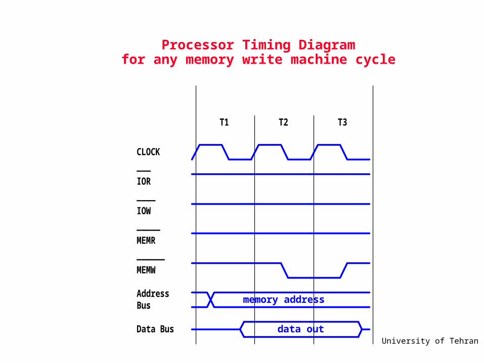
Processor Timing Diagramfor any memory write machine cycle
IOR
IOW
MEMR
MEMW
___
____
_____
______
AddressBus
Data Bus
T1 T2 T3
CLOCK
memory address
data out

University of Tehran 6
When interfacing memory chips to a microprocessor, consider the following:
• TAVDV – address access time
• TRLDV – read access time
• TDVWH – memory setup time
• TWHDX – data hold time
• TWLWH – write pulse width
Refer to 8088 data manual

University of Tehran 7
Address Access Time (TAVDV)
ALE
T1
CLOCK
T2 T3 T4
AD7 - AD0
A15 - A8
A19/S6 - A16/S3
DT/R __
IO/M __
____
RD
DEN______
A19 - A0from 74LS373 to memory
A15 - A8
A19 - A16 S6 - S3
A19 - A0 from 74LS373
D7 - D0from memory to 74LS245
D7 - D0 (from memory)
A7 - A0 D7 - D0 from74LS245
garbage
TAVDV
3TCLCL
TCLAV
TDVCL
University of Tehran 8
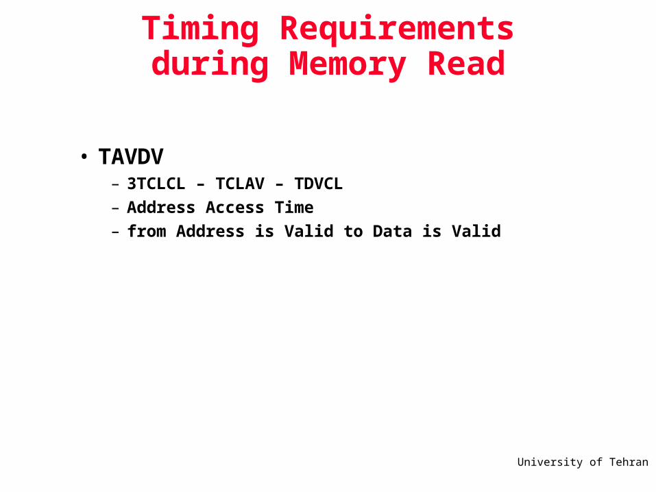
Timing Requirements during Memory Read
• TAVDV– 3TCLCL – TCLAV – TDVCL
– Address Access Time
– from Address is Valid to Data is Valid
University of Tehran 9
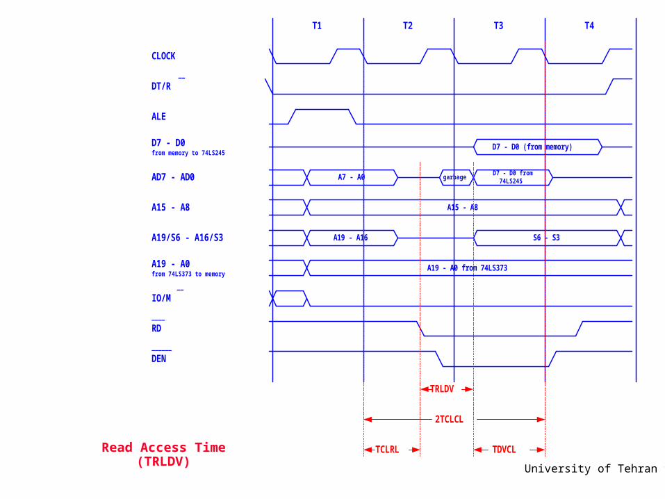
Read Access Time (TRLDV)
ALE
T1
CLOCK
T2 T3 T4
AD7 - AD0
A15 - A8
A19/S6 - A16/S3
DT/R __
IO/M __
____
RD
DEN______
A19 - A0from 74LS373 to memory
A15 - A8
A19 - A16 S6 - S3
A19 - A0 from 74LS373
D7 - D0from memory to 74LS245
D7 - D0 (from memory)
A7 - A0 D7 - D0 from74LS245
garbage
TRLDV
2TCLCL
TDVCLTCLRL

University of Tehran 10
Timing Requirements during Memory Read
• TRLDV– 2TCLCL – TCLRL – TDVCL
– Read Access Time
– from Read Signal is Low to Data is Valid
University of Tehran 11
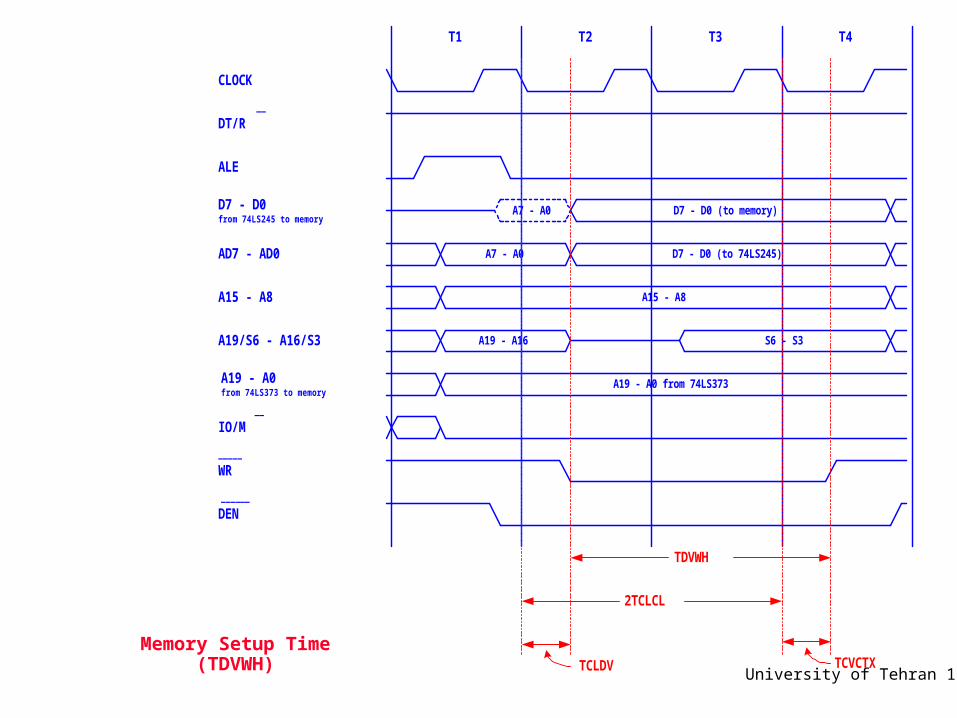
Memory Setup Time (TDVWH)
ALE
T1
CLOCK
T2 T3 T4
AD7 - AD0
A15 - A8
A19/S6 - A16/S3
DT/R __
IO/M __
_____
WR
DEN______
A19 - A0from 74LS373 to memory
A15 - A8
A19 - A16 S6 - S3
A19 - A0 from 74LS373
A7 - A0 D7 - D0 (to 74LS245)
D7 - D0from 74LS245 to memory
D7 - D0 (to memory)A7 - A0
2TCLCL
TDVWH
TCLDV TCVCTX

University of Tehran 12
Timing Requirements during Memory Write
• TDVWH– 2TCLCL – TCLDV +TCVCTX
– Memory Setup Time
– from Data is Valid to Write Signal is High
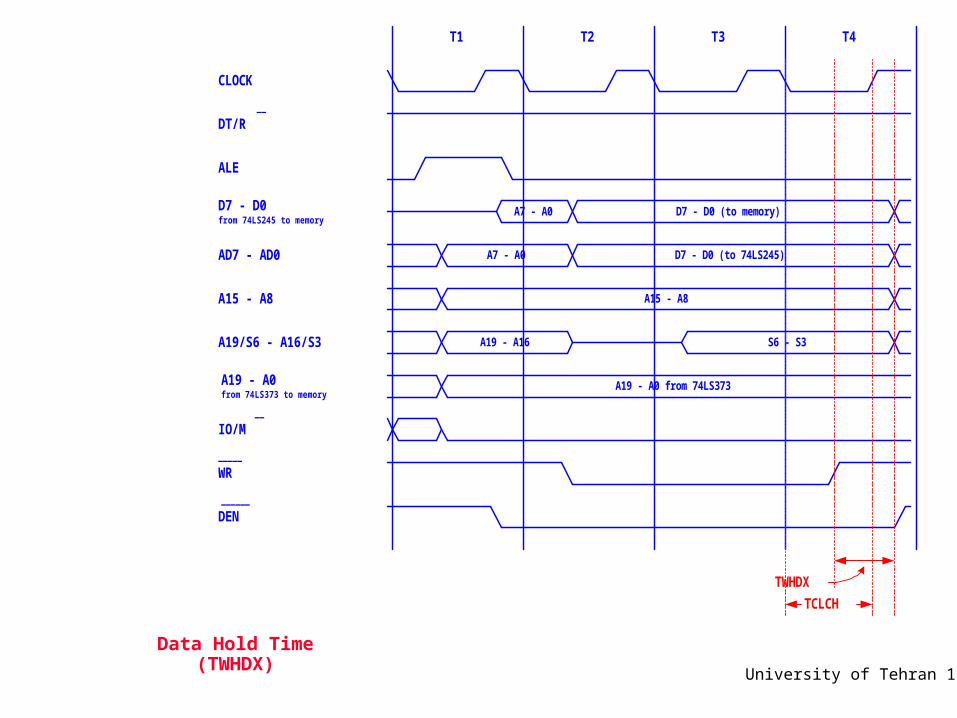
University of Tehran 13Data Hold Time (TWHDX)
ALE
T1
CLOCK
T2 T3 T4
AD7 - AD0
A15 - A8
A19/S6 - A16/S3
DT/R __
IO/M __
_____
WR
DEN______
A19 - A0from 74LS373 to memory
A15 - A8
A19 - A16 S6 - S3
A19 - A0 from 74LS373
A7 - A0 D7 - D0 (to 74LS245)
D7 - D0from 74LS245 to memory
D7 - D0 (to memory)A7 - A0
TWHDX
TCLCH
University of Tehran 14
Timing Requirements during Memory Write
• TWHDX– TCLCH – X
– Data Hold Time (after WR’)
– from Write Signal is High to Data is Invalid (Inactive)

University of Tehran 15
Write Pulse Width / Write-Time (TWLWH)
ALE
T1
CLOCK
T2 T3 T4
AD7 - AD0
A15 - A8
A19/S6 - A16/S3
DT/R __
IO/M __
_____
WR
DEN______
A19 - A0from 74LS373 to memory
A15 - A8
A19 - A16 S6 - S3
A19 - A0 from 74LS373
A7 - A0 D7 - D0 (to 74LS245)
D7 - D0from 74LS245 to memory
D7 - D0 (to memory)A7 - A0
TWLWH
2TCLCL

University of Tehran 16
Timing Requirements during Memory Write
• TWLWH– 2TCLCL – Y
– Write Pulse Width / Write-Time
– from Write Signal is Low to Write Signal is High

University of Tehran 17
8088 MINIMUM COMPLEXITY SYSTEM TIMING REQUIREMENTS
8088 8088-2 Symbol Parameter Min Max Min Max
Units
TCLCL CLK Cycle Period 200 500 125 500 ns
TCLCH CLK Low Time 118 68 ns
TDVCL Data Setup Time 30 20 ns
TCLAV Address Valid Delay 10 110 10 60 ns
TCLRL RD’ Active Delay 10 165 10 100 ns
TCLDV Data Valid Delay 10 110 10 60 ns
TCVCTX Control Inactive Delay 10 110 10 70 ns
TWHDX Data Hold Time after WR’ TCLCH – 30 TCLCH – 30 ns
TWLWH WR’ Width 2TCLCL – 60 2TCLCL – 40 ns

University of Tehran 18
Computation of Timing Requirements for 8088 using a 4Mhz Clock
• TAVDV 3TCLCL – TCLAVmax – TDVCLmin
3(250 ns) – 110 ns – 30 ns 610 ns
• TRLDV 2TCLCL – TCLRLmax – TDVCLmin
3(250 ns) – 165 ns – 30 ns 555 ns

University of Tehran 19
8088 MINIMUM COMPLEXITY SYSTEM TIMING REQUIREMENTS
8088 8088-2 Symbol Parameter Min Max Min Max
Units
TCLCL CLK Cycle Period 200 500 125 500 ns
TCLCH CLK Low Time 118 68 ns
TDVCL Data Setup Time 30 20 ns
TCLAV Address Valid Delay 10 110 10 60 ns
TCLRL RD’ Active Delay 10 165 10 100 ns
TCLDV Data Valid Delay 10 110 10 60 ns
TCVCTX Control Inactive Delay 10 110 10 70 ns
TWHDX Data Hold Time after WR’ TCLCH – 30 TCLCH – 30 ns
TWLWH WR’ Width 2TCLCL – 60 2TCLCL – 40 ns

University of Tehran 20
Computation of Timing Requirements for 8088 using a 4Mhz Clock
• TDVWH 2TCLCL – TCLDVmax +TCVCTXmin
2(250 ns) – 110 ns + 10 ns 400 ns
• TWHDX TCLCH – X 118 ns – 30 ns 88 ns
• TWLWH 2TCLCL – Y 2(250 ns) – 60 ns 440 ns
University of Tehran 21
Timing Requirements for 8088 using a 4Mhz Clock
• TAVDV = 610 ns
• TRLDV = 555 ns
• TDVWH = 400 ns
• TWHDX = 88 ns
• TWLWH = 440 ns

University of Tehran 22
Can we interface a 6264 to the 8088 chip which uses a 4MHz clock?
University of Tehran 23
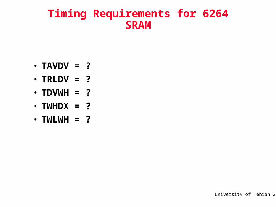
Timing Requirements for 6264 SRAM
• TAVDV = ?
• TRLDV = ?
• TDVWH = ?
• TWHDX = ?
• TWLWH = ?
University of Tehran 24
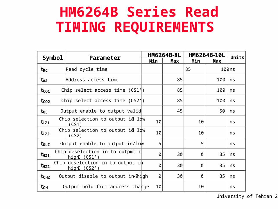
HM6264B Series Read TIMING REQUIREMENTS
HM6264B-8L HM6264B-10L Symbol Parameter Min Max Min Max
Units
tRC Read cycle time 85 100 ns
tAA Address access time 85 100 ns
tCO1 Chip select access time (CS1’) 85 100 ns
tCO2 Chip select access time (CS2’) 85 100 ns
tOE Output enable to output valid 45 50 ns
tLZ1 Chip selection to output in low-Z
(CS1) 10 10 ns
tLZ2 Chip selection to output in low-Z
(CS2) 10 10 ns
tOLZ Output enable to output in low-Z 5 5 ns
tHZ1 Chip deselection in to output i n high- Z (CS1’)
0 30 0 35 ns
tHZ2 Chip deselection in to output in high- Z (CS2’)
0 30 0 35 ns
tOHZ Output disable to output in high-Z 0 30 0 35 ns
tOH Output hold from address change 10 10 ns

University of Tehran 25
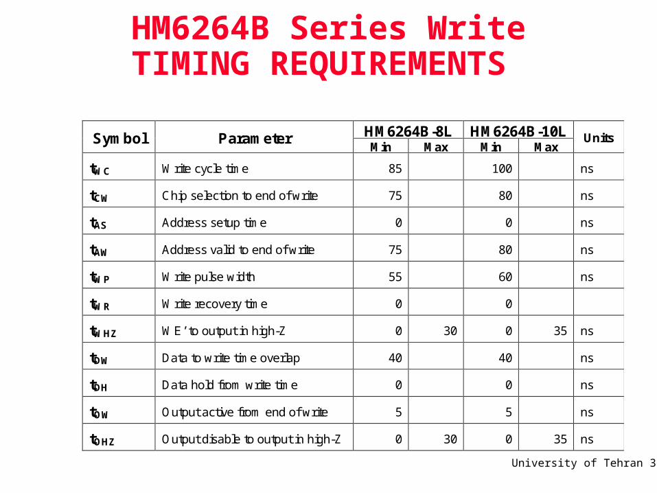
HM6264B Series Write TIMING REQUIREMENTS
HM6264B-8L HM6264B-10L Symbol Parameter Min Max Min Max
Units
tWC Write cycle time 85 100 ns
tCW Chip selection to end of write 75 80 ns
tAS Address setup time 0 0 ns
tAW Address valid to end of write 75 80 ns
tWP Write pulse width 55 60 ns
tWR Write recovery time 0 0
tWHZ WE’ to output in high-Z 0 30 0 35 ns
tDW Data to write time overlap 40 40 ns
tDH Data hold from write time 0 0 ns
tOW Output active from end of write 5 5 ns
tOHZ Output disable to output in high-Z 0 30 0 35 ns
University of Tehran 26
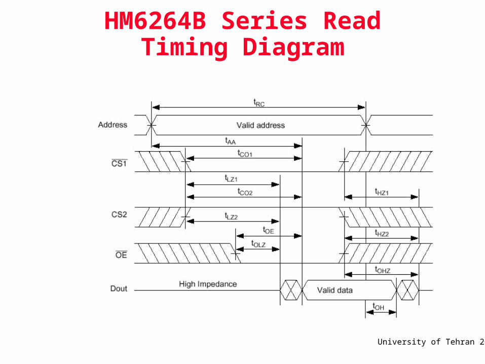
HM6264B Series Read Timing Diagram

University of Tehran 27
HM6264B Series Write Timing Diagram

University of Tehran 28
Timing Requirements for 6264 SRAM
• TAVDV = tAA
• TRLDV = tOE
• TDVWH = tDW
• TWHDX = tDH
• TWLWH = tWP

University of Tehran 29
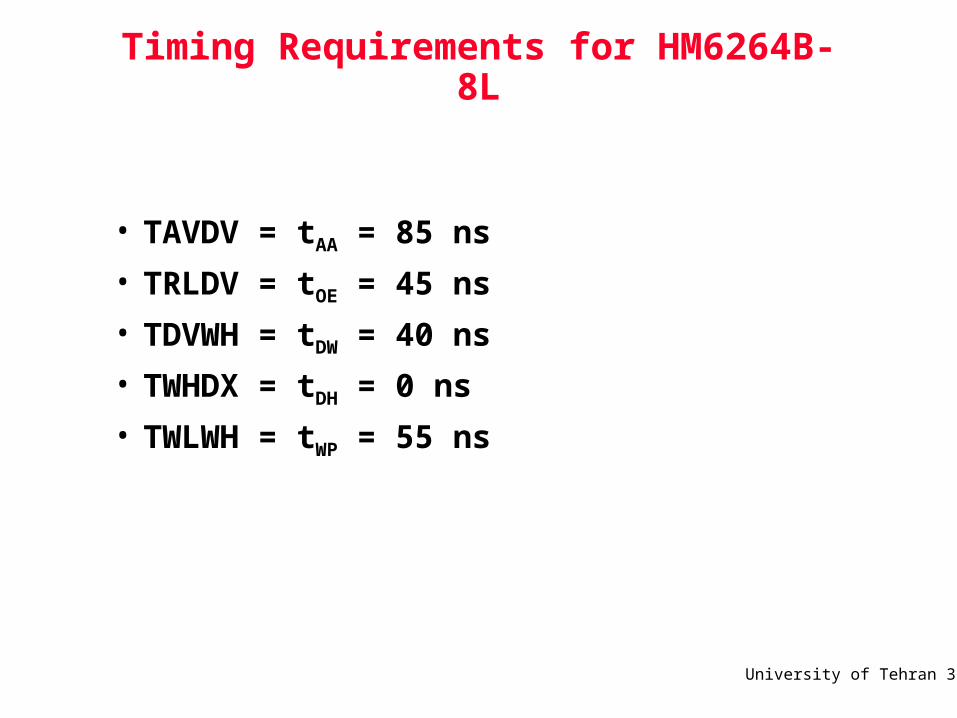
Timing Requirements for HM6264B-8L
• TAVDV = tAA = ?
• TRLDV = tOE = ?
• TDVWH = tDW = ?
• TWHDX = tDH = ?
• TWLWH = tWP = ?

University of Tehran 30
HM6264B Series Read TIMING REQUIREMENTS
HM6264B-8L HM6264B-10L Symbol Parameter Min Max Min Max
Units
tRC Read cycle time 85 100 ns
tAA Address access time 85 100 ns
tCO1 Chip select access time (CS1’) 85 100 ns
tCO2 Chip select access time (CS2’) 85 100 ns
tOE Output enable to output valid 45 50 ns
tLZ1 Chip selection to output in low-Z (CS1)
10 10 ns
tLZ2 Chip selection to output in low-Z (CS2)
10 10 ns
tOLZ Output enable to output in low-Z 5 5 ns
tHZ1 Chip deselection in to output in high-Z (CS1’)
0 30 0 35 ns
tHZ2 Chip deselection in to output in high-Z (CS2’)
0 30 0 35 ns
tOHZ Output disable to output in high-Z 0 30 0 35 ns
tOH Output hold from address change 10 10 ns
University of Tehran 31
HM6264B Series Write TIMING REQUIREMENTS
HM6264B-8L HM6264B-10L Symbol Parameter Min Max Min Max
Units
tWC Write cycle time 85 100 ns
tCW Chip selection to end of write 75 80 ns
tAS Address setup time 0 0 ns
tAW Address valid to end of write 75 80 ns
tWP Write pulse width 55 60 ns
tWR Write recovery time 0 0
tWHZ WE’ to output in high-Z 0 30 0 35 ns
tDW Data to write time overlap 40 40 ns
tDH Data hold from write time 0 0 ns
tOW Output active from end of write 5 5 ns
tOHZ Output disable to output in high-Z 0 30 0 35 ns
University of Tehran 32
Timing Requirements for HM6264B-8L
• TAVDV = tAA = 85 ns
• TRLDV = tOE = 45 ns
• TDVWH = tDW = 40 ns
• TWHDX = tDH = 0 ns
• TWLWH = tWP = 55 ns
University of Tehran 33
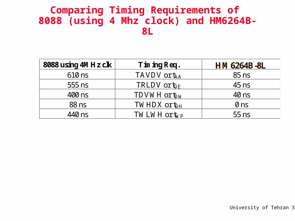
Comparing Timing Requirements of 8088 (using 4 Mhz clock) and HM6264B-8L
8088 using 4MHz clk Timing Req. HM6264B-8L 610 ns TAVDV or tAA 85 ns
555 ns TRLDV or tOE 45 ns 400 ns TDVWH or tDW 40 ns
88 ns TWHDX or tDH 0 ns
440 ns TWLWH or tWP 55 ns

University of Tehran 34
Can we interface a 2764 to the 8088 chip which uses a 4MHz clock?

University of Tehran 35
Timing Requirements for 2764 EPROM
• TAVDV = ?
• TRLDV = ?
• TDVWH = ?
• TWHDX = ?
• TWLWH = ?

University of Tehran 36
M2764A Read Mode AC Characteristics
-3 -4 Symbol Alt Parameter Min Max Min Max
Units
tAVQV tACC Address Valid to Output Valid
180 200 ns
tELQV tCE Chip Enable Low to Output Valid
180 200 ns
tGLQV tOE Output Enable Low to Output Valid
65 75 ns
tEHQZ tDF Chip Enable High to Ourput Hi-Z
0 55 0 55 ns
tGHQZ tDF Output Enable High to Output Hi-Z
0 55 0 55 ns
tAXQX tDH Address Transition to Output Transition
0 0 ns
University of Tehran 37
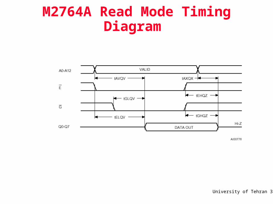
M2764A Read Mode Timing Diagram

University of Tehran 38
Timing Requirements for 2764 EPROM
• TAVDV = tAVQV
• TRLDV = tGLQV
• TDVWH = N/A
• TWHDX = N/A
• TWLWH = N/A

University of Tehran 39
Timing Requirements for 2764 EPROM
• TAVDV = tAVQV = ?
• TRLDV = tGLQV = ?
• TDVWH = N/A
• TWHDX = N/A
• TWLWH = N/A
University of Tehran 40
M2764A Read Mode AC Characteristics
-3 -4 Symbol Alt Parameter Min Max Min Max
Units
tAVQV tACC Address Valid to Output Valid
180 200 ns
tELQV tCE Chip Enable Low to Output Valid
180 200 ns
tGLQV tOE Output Enable Low to Output Valid
65 75 ns
tEHQZ tDF Chip Enable High to Ourput Hi-Z
0 55 0 55 ns
tGHQZ tDF Output Enable High to Output Hi-Z
0 55 0 55 ns
tAXQX tDH Address Transition to Output Transition
0 0 ns
University of Tehran 41
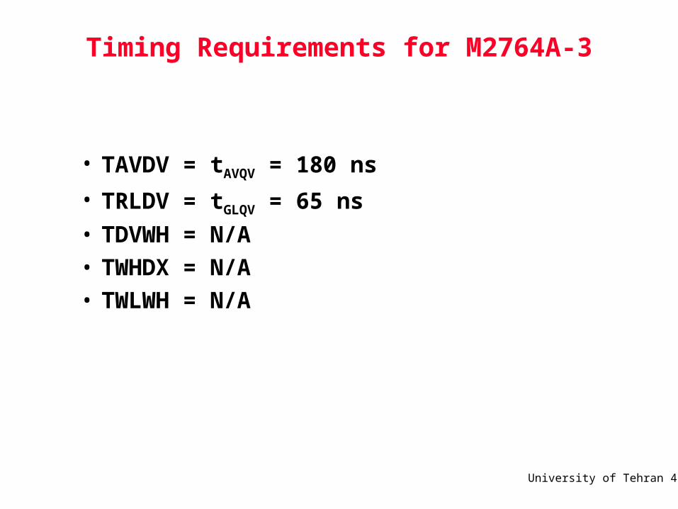
Timing Requirements for M2764A-3
• TAVDV = tAVQV = 180 ns
• TRLDV = tGLQV = 65 ns
• TDVWH = N/A
• TWHDX = N/A
• TWLWH = N/A

University of Tehran 42
Comparing Timing Requirements of 8088 (using 4 Mhz clock) and M2764A-3
8088 using 4MHz clk Timing Req. HM6264B-8L 610 ns TAVDV or tAVQV 180 ns
555 ns TRLDV or tGLQV 65 ns

University of Tehran 43
What if we need to interface a “slow” memory to the 8088?
University of Tehran 44
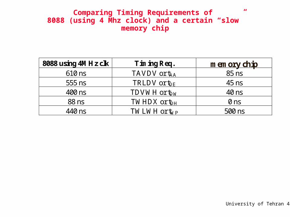
Comparing Timing Requirements of 8088 (using 4 Mhz clock) and a certain “slow” memory chip
8088 using 4MHz clk Timing Req. memory chip 610 ns TAVDV or tAA 85 ns
555 ns TRLDV or tOE 45 ns 400 ns TDVWH or tDW 40 ns
88 ns TWHDX or tDH 0 ns
440 ns TWLWH or tWP 500 ns

University of Tehran 45
8088Minimum
Mode
A12
A0:
D7
D0:
MEMRMEMW
A13A14
HM6264B-8L
A12
A0:
D7
D0:
OEWE
CS1 CS2
SLOWMEMORY
A12
A0:
D7
D0:
RDWR
CS
M2764A-3
A12
A0:
Q7
Q0:
G
C
A15A16A17A18A19
::
5V
READY
University of Tehran 46
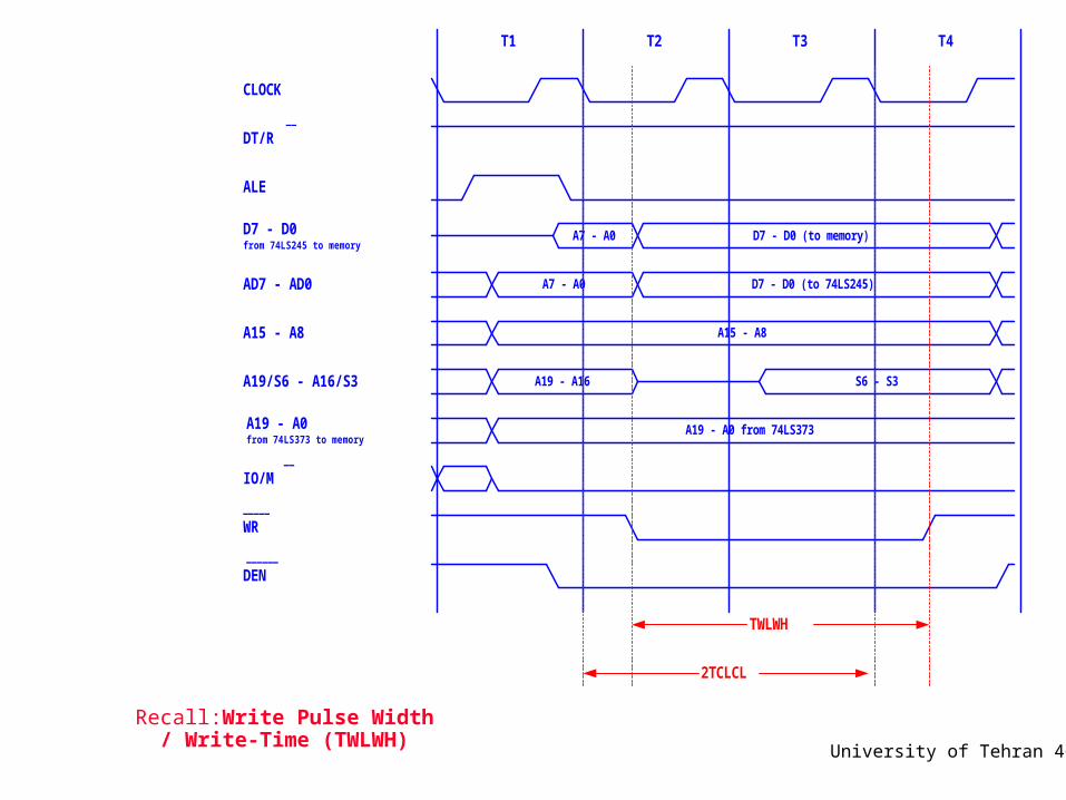
Recall:Write Pulse Width / Write-Time (TWLWH)
ALE
T1
CLOCK
T2 T3 T4
AD7 - AD0
A15 - A8
A19/S6 - A16/S3
DT/R __
IO/M __
_____
WR
DEN______
A19 - A0from 74LS373 to memory
A15 - A8
A19 - A16 S6 - S3
A19 - A0 from 74LS373
A7 - A0 D7 - D0 (to 74LS245)
D7 - D0from 74LS245 to memory
D7 - D0 (to memory)A7 - A0
TWLWH
2TCLCL

University of Tehran 47
Write Pulse Width / Write-Time (TWLWH) w/ 1 wait state
ALE
T1
CLOCK
T2 T4
AD7 - AD0
A15 - A8
A19/S6 - A16/S3
READY
IO/M __
_____
WR
DEN______
A19 - A0from 74LS373 to memory
D7 - D0from 74LS245 to memory
TWLWH
A7 - A0 D7 - D0 (to memory)
A7 - A0 D7 - D0 (to 74LS245)
A15 - A8
A19 - A16 S6 - S3
A19 - A0 from 74LS373
DT/R __
TW T3

University of Tehran 48
Comparing Timing Requirements of 8088 (using 4 Mhz clock) and a certain memory chip
8088 using 4MHz clk Timing Req. memory chip 610 ns TAVDV or tAA 85 ns
555 ns TRLDV or tOE 45 ns 400 ns + 250 ns TDVWH or tDW 40 ns
88 ns + 250 ns TWHDX or tDH 0 ns
440 ns + 250 ns TWLWH or tWP 500 ns
caused by 1 wait state during a memory write on the “slow” memory chip

University of Tehran 49
How do we produce a wait state?
• By turning the READY input of the 8088 microprocessor to LOW

University of Tehran 50
8088Minimum
Mode
A12
A0:
D7
D0:
MEMRMEMW
A13A14
HM6264B-8L
A12
A0:
D7
D0:
OEWE
CS1 CS2
SLOWMEMORY
A12
A0:
D7
D0:
RDWR
CS
M2764A-3
A12
A0:
Q7
Q0:
G
C
A15A16A17A18A19
::
5V
READY

University of Tehran 51Requirements for the READY input of the 8088
ALE
T1
CLOCK
T2 T4
AD7 - AD0
A15 - A8
A19/S6 - A16/S3
READY
IO/M __
_____
WR
DEN______
A19 - A0from 74LS373 to memory
D7 - D0from 74LS245 to memory
30 ns(min)
A7 - A0 D7 - D0 (to memory)
A7 - A0 D7 - D0 (to 74LS245)
A15 - A8
A19 - A16 S6 - S3
A19 - A0 from 74LS373
DT/R __
TW T3
119 ns(min)
as much as possiblethis should be LOW
before the end of T2 (ifit is not possible, it canbe late by at most 8ns)
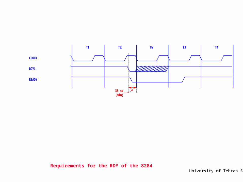
University of Tehran 52Requirements for the RDY of the 8284
T1
CLOCK
T2 T4
RDY1
35 ns(min)
TW T3
READY

University of Tehran 53
8088Minimum
Mode
A12
A0:
D7
D0:
MEMRMEMW
A13A14
HM6264B-8L
A12
A0:
D7
D0:
OEWE
CS1 CS2
SLOWMEMORY
A12
A0:
D7
D0:
RDWR
CS
M2764A-3
A12
A0:
Q7
Q0:
G
C
A15A16A17A18A19
::
5V
READY

University of Tehran 54
Related Documents