UNIVERSIDAD AUTÓNOMA DE NUEVO LEÓN FACULTAD DE INGENIERÍA MECÁNICA Y ELÉCTRICA TESIS COMPUTADORA DE VUELO PARA ADQUISICIÓN DE DATOS CINEMÁTICOS EN TIEMPO REAL EN MICRO AERONAVES POR ING. RUBEN ABISAI CAMPOS CANIZALES EN OPCIÓN AL GRADO DE MAESTRÍA EN INGENIERÍA AERONÁUTICA CON ORIENTACIÓN EN DINÁMICA DE VUELO NOVIEMBRE, 2016

Welcome message from author
This document is posted to help you gain knowledge. Please leave a comment to let me know what you think about it! Share it to your friends and learn new things together.
Transcript

UNIVERSIDAD AUTÓNOMA DE NUEVO LEÓN FACULTAD DE INGENIERÍA MECÁNICA Y ELÉCTRICA
TESIS
COMPUTADORA DE VUELO PARA ADQUISICIÓN DE DATOS
CINEMÁTICOS EN TIEMPO REAL EN MICRO AERONAVES
POR
ING. RUBEN ABISAI CAMPOS CANIZALES
EN OPCIÓN AL GRADO DE MAESTRÍA EN INGENIERÍA AERONÁUTICA CON ORIENTACIÓN EN DINÁMICA DE VUELO
NOVIEMBRE, 2016

UNIVERSIDAD AUTÓNOMA DE NUEVO LEÓN FACULTAD DE INGENIERÍA MECÁNICA Y ELÉCTRICA
SUBDIRECCIÓN DE ESTUDIOS DE POSGRADO
TESIS
COMPUTADORA DE VUELO PARA ADQUISICIÓN DE DATOS CINEMÁTICOS EN TIEMPO REAL EN MICRO AERONAVES
POR
ING. RUBEN ABISAI CAMPOS CANIZALES
EN OPCIÓN AL GRADO DE MAESTRÍA EN INGENIERÍA AERONÁUTICA CON ORIENTACIÓN EN DINÁMICA DE VUELO
SAN NICOLÁS DE LA GARZA, NUEVO LEÓN, MÉXICO NOVIEMBRE, 2016


Dedicatoria Dedico de manera especial a mis padres Guillermo y Alejandra y a mis hermanos Mara, Zabdy y Guillermo, por su importante apoyo para seguir adelante ya que si ellos, no hubiera podido seguir adelante.

Agradecimientos
Quiero agradecer a mi Asesor M.C Daniel Librado Martínez Vázquez por la oportunidad que me dio al trabajar con él, por sus enseñanzas, por sus consejos y sobre todo lecciones de vida que sin duda quedaron marcadas para ponerlas en práctica siempre, a usted muchas gracias.
Agradezco al DR. Eduardo Liceaga Castro por su apoyo, por permitirme estar en su grupo de trabajo, por su paciencia y su apoyo. Agradezco al Dr. Luis A. Amezquita Brooks y al Dr. Octavo García Salazar por permitirme trabajar en los laboratorios de aviónica y navegación. A mis amigos y compañeros Carlos Vaquera, Roberto Fabela, Juan Sánchez, Gabino Ramírez, Carlos Santana, Jaime Aguilar y Diego Rivera por su apoyo, motivación, consejos y sobre todo compañía en todo este trayecto.
TABLA DE CONTENIDO RESUMEN ....................................................................................... 8
1.- INTRODUCCIÓN ....................................................................... 10
1.1 DESCRIPCIÓN DEL PROBLEMA ............................................................................................. 10
1.2 JUSTIFICACIÓN ..................................................................................................................... 11
1.3 OBJETIVO .............................................................................................................................. 12
1.4 HIPÓTESIS ............................................................................................................................. 12
1.5 LÍMITES DE ESTUDIO ............................................................................................................ 12
2.- FUNDAMENTOS ...................................................................... 13
2.1 ESTADO DE LA TECNOLOGÍA ................................................................................................ 13
2.2 MARCO TEÓRICO ................................................................................................................. 14
2.2.1 COMPUTADORA DE VUELO ........................................................................................... 14
2.2.2 VARIABLES DE INTERÉS ................................................................................................. 16
2.3 EJEMPLOS DE COMPUTADORAS DE VUELO ..................................................................... 19
2.4 SISTEMAS EN TIEMPO REAL ............................................................................................. 20
2.4.1 CLASIFICACIÓN DE LOS STR. ...................................................................................... 21
2.4.2 HILOS ......................................................................................................................... 22
2.4.3 CLASIFICACIÓN DE HILOS .......................................................................................... 24
3.- PROCEDIMIENTO ..................................................................... 24
3.1 DISEÑO DE LOS PROCESOS Y DE LA ARQUITECTURA GENERAL ....................................... 24
3.2 ELECCIÓN DE LA COMPUTADORA EMBEBIDA Y SENSORES ............................................. 29
3.2.1 COMPARACIÓN DE COMPUTADORAS EMBEBIDAS .................................................. 29
3.2.2 BEAGLE BONE BLACK ................................................................................................ 30
3.2.3 SENSORES .................................................................................................................. 31
3.2.4 SISTEMA OPERATIVO Y ENTORNO DE PROGRAMACIÓN .......................................... 32
3.3 INTEGRACIÓN DE LA COMPUTADORA DE VUELO ............................................................ 32
3.3.1 DESCRIPCIÓN GENERAL DE LA INTEGRACIÓN ........................................................... 32
3.3.2 CÓDIGO ..................................................................................................................... 32
3.3.3 DIAGRAMA DE CONEXIONES ELÉCTRICAS ................................................................ 33
3.3.4 INTEGRACIÓN FINAL ................................................................................................. 35
3.4 VALIDACIÓN DE LA PLATAFORMA ................................................................................... 36
3.4.1 MEDICIÓN DE LA FRECUENCIA DE TRABAJO ............................................................. 36

3.4.2 INTERFAZ CON MICROAERONAVE ............................................................................ 37
3.4.3 PRUEBA MECÁNICA EN BANCO DE PRUEBAS ........................................................... 39
3.4.3.1 VALIDACIÓN PRELIMINAR EN ALABEO............................................................... 40
3.4.3.2 VALIDACIÓN PRELIMINAR EN CABECEO ............................................................ 41
3.4.3.3 VALIDACIÓN PRELIMINAR EN GUIÑADA. ........................................................... 42
3.4.4 VALIDACIÓN DE LA PLATAFORMA CON SISTEMA VICON ......................................... 42
3.4.5 PRUEBA DE LA PLATAFORMA EN TÚNEL DE VIENTO ................................................ 45
3.4.6 VALIDACIÓN DEL SISTEMA GPS ................................................................................. 46
4.- ANALISIS DE RESULTADOS ....................................................... 47
4.1 VALIDACIÓN DE LAS VARIABLES DE RUMBO Y ACTITUD ..................................................... 47
4.2 PRUBAS EN TÚNEL DE VIENTO ............................................................................................. 50
4.3 VALIDACIÓN DEL SISTEMA GPS ............................................................................................ 53
5.- CONCLUSIÓNES Y RECOCOMENDACIONES ............................. 56
5.1 CONCLUSIONES .................................................................................................................... 56
5.2 TRABAJO A FUTURO ............................................................................................................. 56
REFERENCIAS ................................................................................ 57
ANEXOS ........................................................................................ 58
6.1 ENTORNO DE DESARROLLO ................................................................................................. 58
6.1.1 COMPILACION CRUZADA .............................................................................................. 58
6.2 INSTALACION DE ECLIPSE IDE DENTRO EN DEBIAN ............................................................. 59
6.3 INSTALACION DE JAVA RUNTIME ENVIROMENT (JRE). ........................................................ 61
6.4 CONFIGURACION DE ECLIPSE PARA COMPLIACION CRUZADA. ........................................... 64
6.4.1 Agregando una arquitectura externa y actualizando sistema. ..................................... 64
6.4.2 Instalación de herramientas para una compilación cruzada. ....................................... 65
6.4.3 Configuración IDE ECLIPSE. ........................................................................................... 66
. . CONEXIÓN REMOTA A BEAGLEBONE BLACK U“ANDO REMOTE “Y“TEM EXPLORE ........ 69
6.6 CONFIGURACION DE SENSOR UM7 ..................................................................................... 73
6.7 FICHAS TÉCNICAS MECANISMO DE ROTULAS ...................................................................... 77
6.8 CÓDIGO DE CADA UNO DE LOS PROCESOS.......................................................................... 79
6.9 FICHAS TÉCNICAS (BEAGLE BONE, SENSORES) .................................................................... 79

RESUMEN
El objetivo de esta tesis es el diseño, construcción y prueba de una Computadora
de Vuelo con bajo costo para ser utilizada como herramienta de validación de
algoritmos para procesamiento de datos y control en Vehículos Aéreos No
Tripulados.
Aunque en el mercado actual ya existen CV (computadoras de Vuelo) COTS de
alto rendimiento, estas son de alto costo y cuentan con una arquitectura cerrada,
la cual no permite ver ni modificar el código de los algoritmos utilizados; esta falta
de flexibilidad impide probar algoritmos especializados en el ámbito de la
investigación aeronáutica y de aviónica.
Es posible implementar, utilizando dispositivos electrónicos comercialmente
disponibles y desarrollando algoritmos de procesamiento propios, una
Computadora de Vuelo para Vehículos Aéreos No Tripulados con prestaciones de
tiempo real.
Debido a que es la primera aproximación que se tiene a la construcción y prueba
de una CV dentro del CIIIA-FIME-UANL, se ha decidido limitar los alcances de
este trabajo a tener solamente sensores y plataformas de cómputo de bajo costo
con tamaño reducido.
Además, este trabajo se centró en el diseño de algoritmos de adquisición y
procesamiento de datos necesarios para la obtención de los parámetros
cinemáticos de la aeronave; por lo tanto, no se contempla el uso de datos aire ni
la programación de leyes de control (autopiloto).
Finalmente, las pruebas de validación se realizaron dentro de túnel de viento y en
el laboratorio de navegación.
Como el objetivo es desarrollar un sistema de adquisición de datos cinemáticos, se desarrolló un sistema que puede ser aplicado a una micro aeronave. El sistema es de bajo costo, pero trabaja satisfactoriamente en tiempo real con sensores COTS a una tasa de trabajo de 215 Hz.

Se han validado el sistema tanto en actitud como en rumbo por medio de comparaciones con datos obtenidos de un sistema de medición de la posición en alta resolución.
El sistema de posicionamiento global ha sido probado satisfactoriamente mediante la comparación entre la ruta seguida y la ruta medida por el sistema.
1.- INTRODUCCIÓN
1.1 DESCRIPCIÓN DEL PROBLEMA
En los Vehículos Aéreos No Tripulados (VANTs), es necesario contar con un
sistema de cómputo, comúnmente llamado Computadora de Vuelo (CV), que se
encargue de la obtención, procesamiento y almacenamiento de datos de aire,
datos inerciales, datos de navegación por estimación y datos de posicionamiento.
Además de lo anterior, la computadora de vuelo debe contar con algoritmos que
le permitan actuar sobre las superficies de control de la aeronave para garantizar
su correcto funcionamiento sobre un amplio rango de situaciones, a este
subsistema se le conoce como Autopiloto [1].
En este trabajo se plantea la construcción y prueba de una CV para VANTs, en
particular, se aborda el problema mediante la integración de hardware comercial
(COTS - Commercial Off-The-Shelf) con algoritmos de obtención, procesamiento,
almacenamiento y control propios.
Las contribuciones de este trabajo se verán reflejadas en 2 ejes principales: el
desarrollo de tecnología para probar algoritmos avanzados en Dinámica de Vuelo
y la formación de recursos humanos altamente especializados en Aviónica para
investigación.
Definir el hardware adecuado para realizar las tareas de la CV es un proceso difícil
debido a que se debe de contar con una plataforma de gran capacidad de
procesamiento (número de instrucciones procesadas por segundo), capacidad
para manejar una amplia gama de protocolos de comunicación y contar con un
tamaño reducido. A su vez, es necesario que la CV reciba información de diversos
sensores como acelerómetros, giroscopios, magnetómetros y posicionamiento
absoluto (GPS – Global Positioning System) [2]. Esta información debe ser
procesada y almacenada (si es requerido) para realizar los algoritmos de control
de vuelo necesarios para enviar señales a los servoactuadores de las superficies

de control. En la Figura 1.1 se muestra un diagrama simplificado de la
configuración del hardware en una CV.
Figura 1.1. Diagrama simplificado de la configuración de hardware en una CV para VANT.
Por esta razón, es necesario realizar pruebas, con condiciones controladas, a
diferentes sensores, protocolos de comunicación, algoritmos de procesamiento,
algoritmos de almacenamiento y algoritmos de control del VANT. Se propone
realizar pruebas en tierra tanto en el túnel de viento como en el laboratorio de
navegación [3].
1.2 JUSTIFICACIÓN
Aunque en el mercado actual ya existen CV COTS de alto rendimiento, estas son
de alto costo y cuentan con una arquitectura cerrada, la cual no permite ver ni
modificar el código de los algoritmos utilizados; esta falta de flexibilidad impide
probar algoritmos especializados en el ámbito de la investigación aeronáutica y
de aviónica. Por lo tanto, se ha considerado que la realización de una CV está
justificada de acuerdo con los intereses de investigación y desarrollo tecnológico

del grupo de investigación en Dinámica de Vuelo del Centro de Investigación e
Innovación en Ingeniería Aeronáutica de la Fime-Uanl y además se encuentra
alineado con el Plan Nacional de Desarrollo México 2013-2018, el cual cita: “Hacer
del desarrollo científico, tecnológico y la innovación pilares para el progreso
económico y social sostenible,… Impulsar el desarrollo de las vocaciones y
capacidades científicas, tecnológicas y de innovación locales, para fortalecer el
desarrollo regional sustentable e incluyente”.
1.3 OBJETIVO
El objetivo de este trabajo es el diseño, construcción y prueba de una
Computadora de Vuelo con bajo costo para ser utilizada como herramienta de
validación de algoritmos para procesamiento de datos y control en Vehículos
Aéreos No Tripulados.
1.4 HIPÓTESIS
Es posible implementar, utilizando dispositivos electrónicos comercialmente
disponibles y desarrollando algoritmos de procesamiento propios, una
Computadora de Vuelo para Vehículos Aéreos No Tripulados con prestaciones de
tiempo real.
1.5 LÍMITES DE ESTUDIO
Debido a que es la primera aproximación que se tiene a la construcción y prueba
de una CV dentro del CIIIA-FIME-UANL, se ha decidido limitar los alcances de
este trabajo a tener solamente sensores y plataformas de cómputo de bajo costo
con tamaño reducido. Además, este trabajo se centrará en el diseño de algoritmos
de adquisición y procesamiento de datos necesarios para la obtención de los
parámetros cinemáticos de la aeronave; por lo tanto, no se contempla el uso de
datos aire ni la programación de leyes de control (autopiloto). Finalmente, las
pruebas de validación se realizarán en tierra, en particular mediante pruebas
dentro de túnel de viento y en el laboratorio de navegación.
2.- FUNDAMENTOS
2.1 ESTADO DE LA TECNOLOGÍA
Dentro de los enlaces de comunicación comunes como Radio Frecuencia (RF),
se proponen otro tipo de comunicación por medio de Sistemas Global para
comunicaciones móviles GSM (del inglés Global System for Mobile
communications) , para establecer Protocolos punto a punto (PPP) entre dos
estaciones móviles , usados comúnmente para intercambio de datos y voz. Otro
tipo de transmisión puede ser por Servicio General de Paquetes vía Radio (del
inglés General Packet Ratio Services 2.5G ) GPRS [4].
En 2004 se realizaron experimentaciones con hardware que era de gran peso y
alto costo y la aviónica tenía un peso aproximado de 15.8 Kg (35 libras), de la
configuración de la aviónica en esta rama de investigación se utilizó un procesador
Pentium II PC Embedded 266 MHz , 500 Mb Flash Drive , Inertial Science ISIS-
IMU (inertial measurement unit) , GPS Diferencial , Magnetómetro de 3 ejes
,protocolos de comunicación usados entre dispositivos son por RS-232 [5] .
En 2005 se requiere utilizar aviónica de bajo, de las desventajas son el uso de
sensores que proporcionan una baja exactitud en comparación con la gama alta
que cuesta más de 100 millones cada unidad. Para superar esta deficiencia se
utilizan sensores de bajo costo que se pueden combinar, en la integración de
estos sensores se tiene el potencial de eliminar las desventajas que existen en
cada sensor. Dentro de los sensores utilizados son Acelerómetros, Giroscopios y
GPS [6].
En 2010 se presenta un modelo de la arquitectura de aviónica modular integrada
de bajo costo el cual está compuesta principalmente por sistemas de navegación
comercialmente disponibles como AHRS (del ingles Attitude Heading Reference
System) de tipo MEMS , GPS , magnetómetro , unidad de procesamiento con
soporte para sistema operativo en tiempo real (RTOS) [7].

En otra Investigación realizada en agosto del 2008 se trabajó sobre la plataforma
modular para aviónica donde el propósito fue presentar una arquitectura para una
gran variedad de prototipos UAV’s para la investigación académica y
organizaciones de investigación, la arquitectura propuesta está compuesta por
una unidad autopiloto miniaturizada , una unidad de almacenamiento , un conjuto
de sensores , un procesador de instrucciones y un sistema de comunicación para
intercambio de información y transmisión de comandos. Dentro del procesador
implementado en la investigación en 2010 se utilizó un procesador de 32-bits
66MHz Freescale ColdFire 5213 utilizado como cerebro del sistema, y en el
conjunto de sensores se utilizaron tipo MEMS compuesto por acelerómetros,
giroscopios, magnetómetros con una tasa de actualización de 50 Hz, además de
un GPS Novatel de 20 Hz [8].
Recientemente se ha evaluado sistemas embebidos basados en productos
comercialmente disponibles COTS ( Commercial off-the-shelf ) , compuesto por
un microcontrolador (µC) MBED NXP LPC1768 de 32-bits ARM Cortex M3 el cual
opera a 96 MHz , un GPS U-BLOX así como una IMU de bajo costo CHR-UM6 el
cual estima los ángulos de Euler usando un filtro de Kalman Extendido (EKF)
combinando datos como los tres ejes del giroscopio , tres ejes del magnetómetro
y tres ejes del acelerómetro , la selección de esta IMU se debe sistema de código
abierto y popularidad en sistemas de bajo costo [9].
2.2 MARCO TEÓRICO
2.2.1 COMPUTADORA DE VUELO
Una computadora de vuelo (CV) es uno de los sistemas más importantes y
fundamentales para el guiado, navegación y control de un vehículo aéreo no
tripulado. La CV se encarga de recabar información de los sensores para poder
ejecutar los algoritmos propios del sistema y poder enviar señales para mover las
superficies de control de la aeronave. La CV debe contar con algoritmos que le
permitan actuar sobre las superficies de control de la aeronave para garantizar su
correcto funcionamiento sobre un amplio rango de situaciones, a este subsistema
se le conoce como Autopiloto.
Los autopilotos son sistemas para guiar a los Vehículos Aéreos No Tripulados
(VANT’s) sin asistencia de operadores humanos. Sin embargo, fueron
desarrollaron en primer lugar para misiles y tiempo después se extendió hacia
aviones y barcos en los años de 1910. Como mínima configuración un sistema
autopiloto debe de incluir sensores de posición y un procesador de instrucciones
[10].
El objetivo de un sistema autopiloto es guiar constantemente una aeronave para
seguir rutas de referencia o navegar a través de puntos de referencia. Un
autopiloto ideal es aquel que puede guiar en todas las etapas: despegue, ascenso,
descenso, trayectoria y arrieraje [11].
Las variables más importantes con las que debe de contar una computadora de
vuelo son las aceleraciones lineales, las velocidades angulares y los datos aire.
La unidad de medición inercial (IMU - Inertial Measurement Unit), es el dispositivo
electrónico que permite medir las aceleraciones lineales y las velocidades
angulares; está compuesta por acelerómetros, giroscopios, magnetómetro,
receptor GPS y sistemas de acondicionamiento y procesamiento de señales. Una
IMU se encarga solo sensar y entregar las velocidades y aceleraciones, el cual
puede ser utilizado para medir la actitud (Alabeo , cabeceo , guiñada ) de un ojeto
en movimiento en el espacio como (un misil, aeronaves o satélites ).
Este tipo de sistemas son utilizados por los pilotos automáticos para poder
controlar o maniobrar el rumbo y trayectoria de un objeto no tripulado.
La tecnología MEMS (MicroElectroMechanical System – Sistema micro-
electromecánico) actual permite que los acelerómetros, giroscopios y
magnetómetros estén dispuestos en grupos de tres ejes ortogonales individuales
pero que están integrados en un mismo chip; además la tecnología MEMS cuenta
con las ventajas de tener menor consumo energético, tener mayor sensibilidad y
ser más económicos que sus antiguos análogos mecánicos, hoy en desuso.

2.2.2 VARIABLES DE INTERÉS
Es posible obtener la velocidad y posición del objeto a partir de la aceleración
medida del marco inercial por medio de la integración como se muestra en la
siguiente ecuación. = ∫
Así como la posición del objeto a partir de la velocidad o aceleración. = ∬
Debido a que en nuestro sistema se requieren que las ecuaciones estén en
tiempo discreto se presentan a continuación:
Velocidad [ + 1] = [ ] + [ ] Posición [ + 1] = [ ] + [ ]
Donde T es el periodo de muestro, V es la velocidad y P es la posición.
Las variables de interés como la posición angular de una aeronave: alabeo,
cabeceo y guiñada son las variables que determinan en última instancia el
comportamiento de cómo se desplaza el objeto en el aire en la figura 2.1 se
muestra estas variables dinámicas.
Figura 2.1 Variables angulares de posición de un Objeto.

Cada una de estas variables angulares están dadas en grados ( ° ) . Así como su
cambio en el tiempo se denomina velocidad angular ( Ω) , y su unidad está
representada en grados por segundo (°/s).
Para poder obtener las señales físicas de estas variables angulares de un objeto
se realiza a través de giróscopos, estos dispositivos usualmente basan su
funcionamiento en fenómenos ópticos (giróscopos laser), mecánicos (giróscopos
electromecánicos), por mencionar algunos.
La unidad de medición de estas variables angulares (alabeo, cabeceo, guiñada)
son los grados [˚]. El cambio de estas variables angulares en el tiempo se
denomina velocidad angular y su unidad son los grados por segundo.
Una IMU con los datos que entrega no puede darnos valores angulares de Alabeo,
Cabeceo, Guiñada, en lugar de darnos estas variables de interés nos proporciona
un valor proporcional a la velocidad angular de cada eje (x , y ,z) , basándonos en
estos valores se debe de deducir que al integrar la velocidad angular se obtendrá
la posición angular :
= ∫ +
Donde C es una constante de integración que aparece al realizar la integral de
una función, algo importante a recalcar es que esta constante ocasiona deriva o
errores de medida que se acumulan con el tiempo.
Es posible obtener la posición angular utilizando el acelerómetro de tres ejes por
medio de leyes trigonométricas así que es posible determinar la actitud de la nave:

Figura 2.2 Vector de Fuerza R en ejes X,Y,Z
Los ángulos que nos interesa definir se encuentran en la Figura 2.2 como Axr ,
Ayr , Azr y así que podemos determinar como :
cos =
cos =
cos =
Aplicando el teorema de Pitágoras en 3D: = √ 2 + 2 + 2
Las variables de interés son los ángulos de posición Axr, Ayr, Azr se pueden
obtener de:
= ( )
= ( )
= ( )
Uno dato importante a aclarar es que el uso de estos ángulos obtenidos por los
acelerómetros no es viable en sistemas de un periodo de trabajo extenso, debido
a su naturaleza donde existe demasiado ruido y no es posible realizar la medida
directamente, comparándola con la lectura a partir de un giroscopio que es más
estable, pero con el tiempo tiende a tener deriva.
Debido a las perturbaciones que existen en los sistemas de autopiloto, a la hora
de adquirir datos provoca que los datos de salida no sean parecidos a la realidad
esperada, por ejemplo, cuando se adquieren los datos del giroscopio o
acelerómetro tienden a volverse inestable con el tiempo. Para evitar este tipo de
problemas comúnmente se opta por utilizar filtros kalman, el cual es un algoritmo
para procesar datos de manera iterativa y su aplicación seria estimar y predecir el
movimiento de una variable que no observamos, pero cuyo efecto podemos
sensar.
2.3 EJEMPLOS DE COMPUTADORAS DE VUELO
En la actualidad existen en el mercado CV de las cuales están elaboradas para el
público en general, comúnmente utilizan controladores PID, el cual ayudan al
usuario a configurarlo de manera rápida solo ajustando las ganancias por medio
de prueba y error hasta que el usuario sea capaz de percibir que el vehículo se
encuentra estable, sin embargo, no es la mejor opción ya que se pueden presentar
problemas en el vehículo y podrían desestabilizarse en cualquier momento.
En la siguiente tabla 2.1 se presentan algunas opciones de CV comerciales e
información de las capacidades de las mismas.
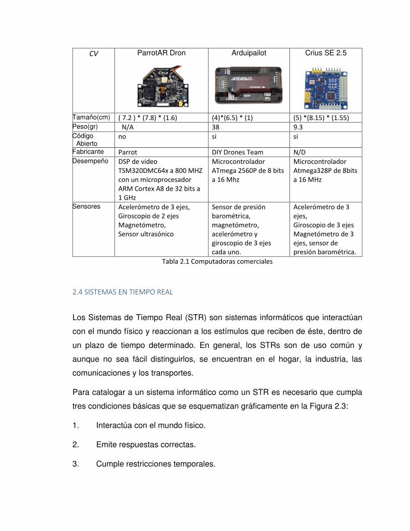
CV ParrotAR Dron
Arduipailot
Crius SE 2.5
Tamaño(cm) ( 7.2 ) * (7.8) * (1.6) (4)*(6.5) * (1) (5) *(8.15) * (1.55) Peso(gr) N/A 38 9.3 Código
Abierto no si si
Fabricante Parrot DIY Drones Team N/D Desempeño DSP de video
TSM320DMC64x a 800 MHZ con un microprocesador ARM Cortex A8 de 32 bits a 1 GHz
Microcontrolador ATmega 2560P de 8 bits a 16 Mhz
Microcontrolador Atmega328P de 8bits a 16 MHz
Sensores Acelerómetro de 3 ejes, Giroscopio de 2 ejes Magnetómetro, Sensor ultrasónico
Sensor de presión barométrica, magnetómetro, acelerómetro y giroscopio de 3 ejes cada uno.
Acelerómetro de 3 ejes, Giroscopio de 3 ejes Magnetómetro de 3 ejes, sensor de presión barométrica.
Tabla 2.1 Computadoras comerciales
2.4 SISTEMAS EN TIEMPO REAL
Los Sistemas de Tiempo Real (STR) son sistemas informáticos que interactúan
con el mundo físico y reaccionan a los estímulos que reciben de éste, dentro de
un plazo de tiempo determinado. En general, los STRs son de uso común y
aunque no sea fácil distinguirlos, se encuentran en el hogar, la industria, las
comunicaciones y los transportes.
Para catalogar a un sistema informático como un STR es necesario que cumpla
tres condiciones básicas que se esquematizan gráficamente en la Figura 2.3:
1. Interactúa con el mundo físico.
2. Emite respuestas correctas.
3. Cumple restricciones temporales.
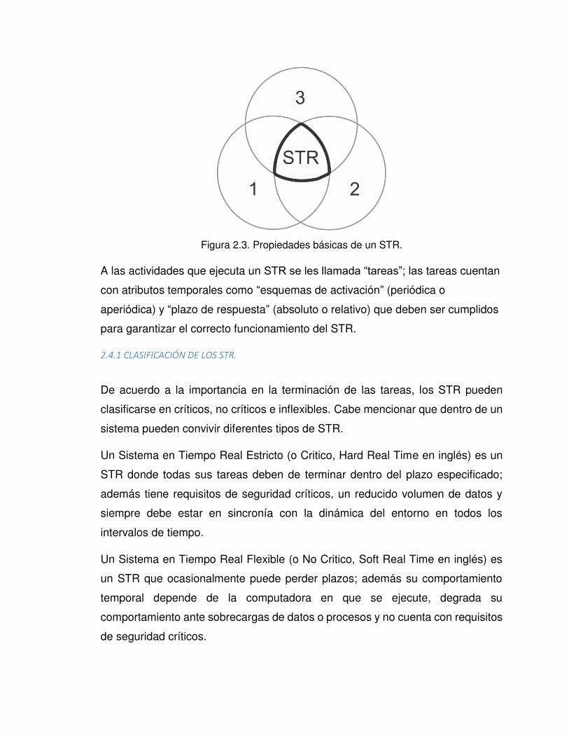
Figura 2.3. Propiedades básicas de un STR.
A las actividades que ejecuta un STR se les llamada “tareas”; las tareas cuentan
con atributos temporales como “esquemas de activación” (periódica o
aperiódica) y “plazo de respuesta” (absoluto o relativo) que deben ser cumplidos
para garantizar el correcto funcionamiento del STR.
2.4.1 CLASIFICACIÓN DE LOS STR.
De acuerdo a la importancia en la terminación de las tareas, los STR pueden
clasificarse en críticos, no críticos e inflexibles. Cabe mencionar que dentro de un
sistema pueden convivir diferentes tipos de STR.
Un Sistema en Tiempo Real Estricto (o Critico, Hard Real Time en inglés) es un
STR donde todas sus tareas deben de terminar dentro del plazo especificado;
además tiene requisitos de seguridad críticos, un reducido volumen de datos y
siempre debe estar en sincronía con la dinámica del entorno en todos los
intervalos de tiempo.
Un Sistema en Tiempo Real Flexible (o No Critico, Soft Real Time en inglés) es
un STR que ocasionalmente puede perder plazos; además su comportamiento
temporal depende de la computadora en que se ejecute, degrada su
comportamiento ante sobrecargas de datos o procesos y no cuenta con requisitos
de seguridad críticos.
Un Sistema en Tiempo Real Firme (o Inflexibles, Firm Real Time en inglés) es un
STR que ocasionalmente puede perder plazos, pero en los que una respuesta
tardía no tiene valor; es decir, si no se respetan las restricciones temporales no
sirve el servicio que proporciona, y por lo tanto, el STR no es funcional dentro de
ese plazo.
2.4.2 HILOS
Las tareas de un STR, por lo general, son ejecutadas concurrentemente mediante
estructuras de procesamiento llamadas hebras o “hilos” (threads). Los hilos son
útiles por que permiten que el flujo del programa sea divido en dos o más partes,
cada una trabajando de manera independiente según los flujos de datos y eventos
pero, coordinados por un programa supervisor llamado planificador (scheduler en
inglés).
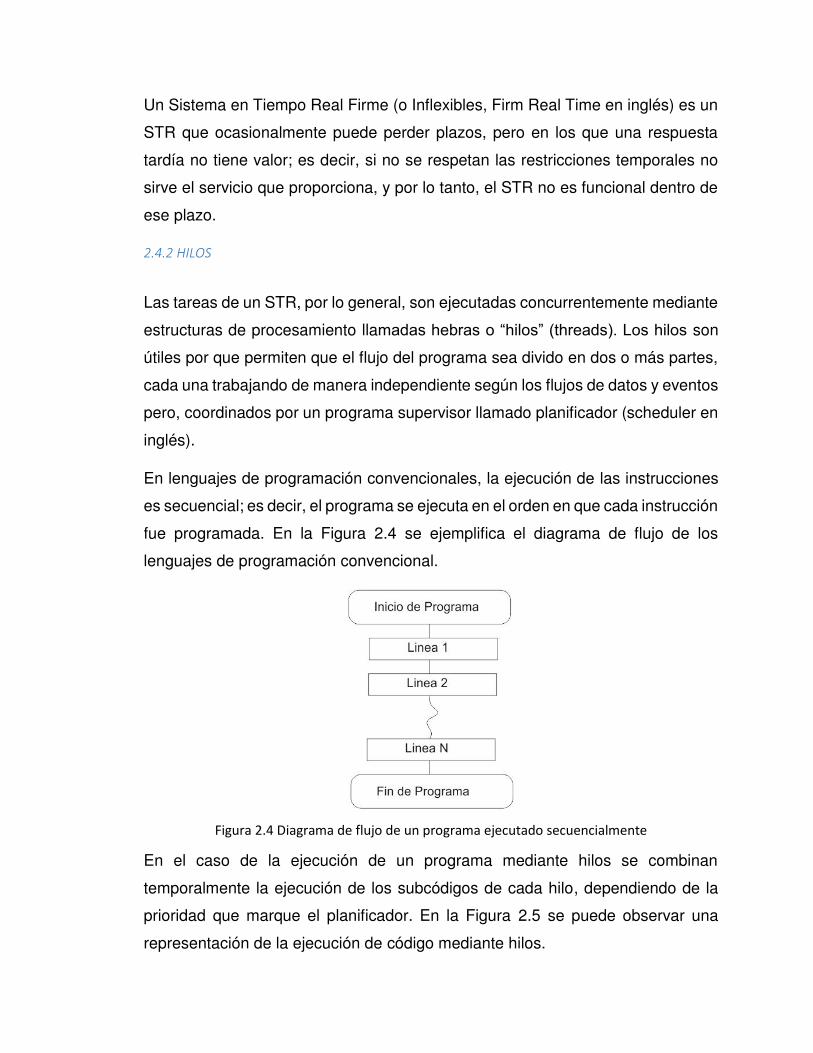
En lenguajes de programación convencionales, la ejecución de las instrucciones
es secuencial; es decir, el programa se ejecuta en el orden en que cada instrucción
fue programada. En la Figura 2.4 se ejemplifica el diagrama de flujo de los
lenguajes de programación convencional.
Figura 2.4 Diagrama de flujo de un programa ejecutado secuencialmente
En el caso de la ejecución de un programa mediante hilos se combinan
temporalmente la ejecución de los subcódigos de cada hilo, dependiendo de la
prioridad que marque el planificador. En la Figura 2.5 se puede observar una
representación de la ejecución de código mediante hilos.

En la Figura 2.5 se puede observar una representación de la ejecución de código mediante hilos
De igual manera en la figura 2.6 se puede observar como el planificador toma el
control y decide cómo se ejecutará el código siempre y cuando no existan
semáforos que controlen el flujo del sistema dependiendo de los eventos que se
estén desarrollando en el transcurso o evolución de la ejecución del programa.
Figura 2.6 se puede observar como el planificador toma el control y decide cómo se ejecutará el
código mediante hilos
2.4.3 CLASIFICACIÓN DE HILOS
Se definen tres tipos de hilos: usuario, kernel e híbrido. Los hilos de usuario (ULT
User-Level Threads) son manejados desde una biblioteca estándar de hilos y su
política de planificación se controla desde la propia aplicación. Las ventajas de
usar ULT son que no se requiere del manejo del sistema a nivel kernel, se puede
optimizar el funcionamiento a nivel aplicación y la aplicación corre sobre cualquier
sistema operativo que soporte librerías de hilos.
Como su nombre lo sugiere, los hilos de kernel (KLT Kernel-Level Threads) son
ejecutados a nivel del procesamiento del kernel. Las ventajas de usar KLTs es
que se pueden planificar, simultáneamente, múltiples hilos del mismo proceso en
múltiples procesadores; en caso de que se bloquee un hilo, el mismo sistema
puede planificar otro proceso para sustituir al hilo bloqueado además de que existe
la posibilidad de que el mismo kernel puede ser multihilo.
Los hilos híbridos (KLT-ULT) son la combinación de ULT y KLT en donde los
múltiples hilos de la aplicación se pueden ejecutar en paralelo en múltiples
procesadores, así mismo, las llamadas al sistema no requieren bloquear todo el
proceso.
3.- PROCEDIMIENTO
3.1 DISEÑO DE LOS PROCESOS Y DE LA ARQUITECTURA GENERAL
Los procesos llevados a cabo en este trabajo se muestran en la Figura 3.1, la cual
está compuesta de los siguientes pasos: 1) Inicializar GPIOS, 2) Crear Archivo
para registradora de datos, 3) Adquisición de datos, 4) procesamiento de datos,
5) almacenamiento de datos, 6) Control a salidas PWM, 7) Transmisión de
información.

Figura 3.1 Diagrama de flujo del proceso general.
En el proceso de inicializar los GPIOS como se muestra las Figura 3.2 este
proceso engloba desde seleccionar el GPIO (General Purpose Input/Output,
Entrada/Salida de Propósito General) y configurarlo como salida o entrada y valor
inicial , así como la configuración del puerto UART (Universal Asynchronous
Receiver-Transmitter, Transmisor-Receptor Asíncrono Universal) , para su
velocidad en este caso 115200 baudios , además se asigna el tamaño de buffer a
utilizar para la trasferencia de datos en este caso 512 bytes. Además, y por último
se configura PWM (pulse width modulation, modulación por ancho o de pulso)
seleccionado el slot a utilizar, así como establecer el periodo y el ciclo de trabajo
inicial.
Figura 3.2 Inicialización de GPIOS.
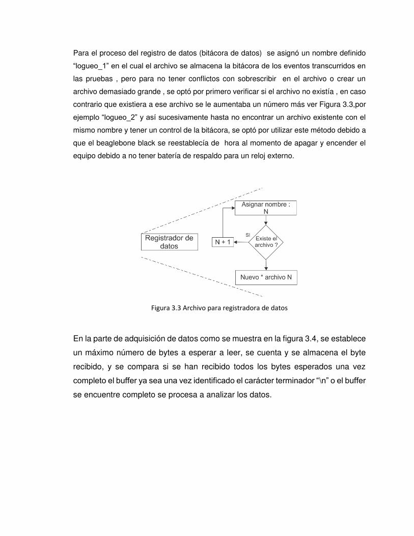
Para el proceso del registro de datos (bitácora de datos) se asignó un nombre definido
“logueo_1” en el cual el archivo se almacena la bitácora de los eventos transcurridos en
las pruebas , pero para no tener conflictos con sobrescribir en el archivo o crear un
archivo demasiado grande , se optó por primero verificar si el archivo no existía , en caso
contrario que existiera a ese archivo se le aumentaba un número más ver Figura 3.3,por
ejemplo “logueo_2” y así sucesivamente hasta no encontrar un archivo existente con el
mismo nombre y tener un control de la bitácora, se optó por utilizar este método debido a
que el beaglebone black se reestablecía de hora al momento de apagar y encender el
equipo debido a no tener batería de respaldo para un reloj externo.
Figura 3.3 Archivo para registradora de datos
En la parte de adquisición de datos como se muestra en la figura 3.4, se establece
un máximo número de bytes a esperar a leer, se cuenta y se almacena el byte
recibido, y se compara si se han recibido todos los bytes esperados una vez
completo el buffer ya sea una vez identificado el carácter terminador “\n” o el buffer
se encuentre completo se procesa a analizar los datos.
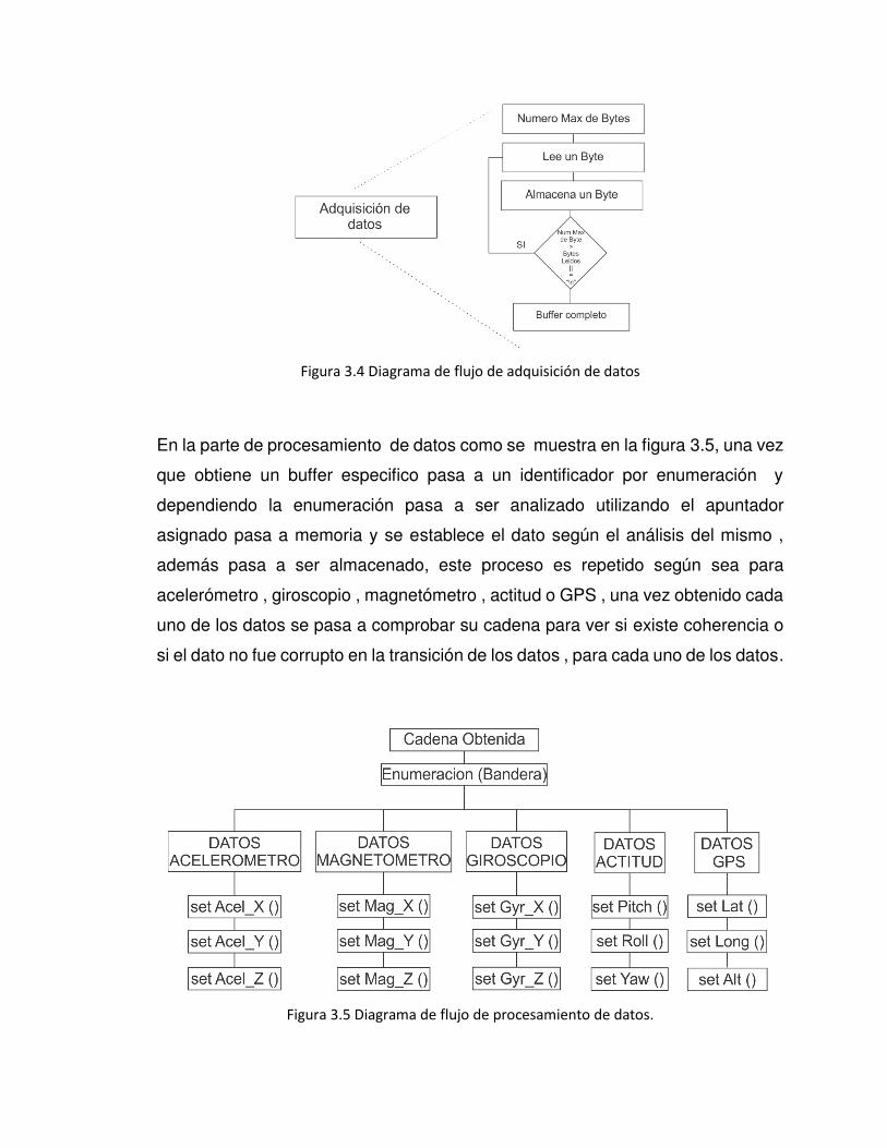
Figura 3.4 Diagrama de flujo de adquisición de datos
En la parte de procesamiento de datos como se muestra en la figura 3.5, una vez
que obtiene un buffer especifico pasa a un identificador por enumeración y
dependiendo la enumeración pasa a ser analizado utilizando el apuntador
asignado pasa a memoria y se establece el dato según el análisis del mismo ,
además pasa a ser almacenado, este proceso es repetido según sea para
acelerómetro , giroscopio , magnetómetro , actitud o GPS , una vez obtenido cada
uno de los datos se pasa a comprobar su cadena para ver si existe coherencia o
si el dato no fue corrupto en la transición de los datos , para cada uno de los datos.
Figura 3.5 Diagrama de flujo de procesamiento de datos.

Por otro lado el proceso de almacenamiento de datos como se muestra en la
figura 3.6, una vez que obtiene un buffer especifico pasa a un identificador por
enumeración y dependiendo la enumeración pasa a ser analizado utilizando el
apuntador asignado ,este se asigna a memoria y se establece el dato según el
análisis del mismo , además pasa a ser almacenado en el archivo de texto, este
proceso es repetido según sea para acelerómetro , giroscopio , magnetómetro ,
actitud o GPS , una vez obtenido cada uno de los datos se pasa a comprobar su
cadena para ver si existe coherencia o si el dato no fue corrupto en la transición
de los datos , para cada uno de los datos.
Figura 3.6 Diagrama de flujo de Almacenamiento de datos en archivo.
En este trabajo se desarrolló la programación para la adquisición de datos, los
cuales son obtenidos por hardware comercial COTS y proporciona datos de:
acelerómetros, giroscopios, magnetómetros y GPS.
Como se muestra en la figura 3.7 se presenta la arquitectura de la computadora
de vuelo para la adquisición de datos cinemáticos en tiempo real, los elementos
que componen la arquitectura son: un procesador ARM que tenga interfaz para
comunicación UART, I2C, PWM , demás tiene un GPS y sensores comercialmente
disponibles (COTS) como el UM7 el cual está compuesto por acelerómetro ,
giroscopio, magnetómetro.

Fig. 3.7 Diagrama de bloques de Arquitectura general
3.2 ELECCIÓN DE LA COMPUTADORA EMBEBIDA Y SENSORES
3.2.1 COMPARACIÓN DE COMPUTADORAS EMBEBIDAS
Como primer paso para elegir la computadora embebida con la que se realizó el
proyecto, fue necesario realizar una búsqueda y una comparación entre las
computadoras accesibles en el estado de la tecnología. Se realizó una lista en
donde se comparan las computadoras encontradas dependiendo del tipo de
procesador, numero de núcleos, velocidad de procesamiento y el costo, que son
las principales características que se tomaron en cuenta para seleccionar la
computadora final. El extracto de la búsqueda y comparación entre computadoras
disponibles se muestra en la tabla 3.1

Tipo Familia de Procesador Tipo de procesador Procesos Nucleos Velocidad Red Costo
Raspberry Pi Model B ARM1176 Broadcom 2835 40nm 1 700MHz 10/100 USB $35
Raspberry Pi Model B+ ARM1176 Broadcom 2835 40nm 1 700MHz 10/100 USB $35
Gumstix Overo ARM Cortex A8 TI OMAP3530 65nm 1 800MHz 10/100 $199
Beagleboard-xm ARM Cortex A8 TI DM3730 45nm 1 1GHz 10/100 $149
Beaglebone Black ARM Cortex A8 TI AM3358/9 45nm 1 1GHz 10/100 $45
Pandaboard ES ARM Cortex A9 TI OMAP4460 45nm 2 1.2GHz 10/100 $199
Trimslice ARM Cortex A9 NVIDIA Tegra2 40nm 2 912MHz 10/100 $99
Cubieboard2 ARM Cortex A7 AllWinner A20 40nm 2 1.7GHz 10/100/1000 $60
Chromebook ARM Cortex A15 Exynos 5 Dual 32nm 2 1.6GHz Wireless $184
ODROID-xU ARM Cortex A7/A15 Exynos 5 Octa 28nm 4 1.2GHz 10/100 $169
Tabla 3.1 Comparación entre microprocesadores costo-velocidad
3.2.2 BEAGLE BONE BLACK
Después de realizar un análisis entre las computadoras disponibles, se eligió a
trabajar con la tarjeta BeagleBone Black debido a su bajo costo, su flexibilidad de
su plataforma de código abierto (open source), la velocidad del reloj de
procesamiento, la cantidad de GPIOS (General Purpose Inputs-Outputs)
disponibles y los protocolos de comunicación disponibles (UART, SPI, I2C). La
imagen ilustrativa del BeagleBone Black se presenta en la Figura 3.8 , así como
las medidas de la computadora (PCB) se presentan en la figura 3.9 y la ficha
técnica completa se presenta como apéndice.
Figura 3.8 Tarjeta BEAGLEBONE BLACK.

Figura 3.9 Dimensiones marcadas se encuentran en milímetros.
3.2.3 SENSORES
A lo largo del desarrollo de este trabajo se tuvieron que probar diferentes tipos de
sensores, desde combinaciones discretas de acelerómetros, giróscopos y
magnetómetros hasta sensores totalmente integrados que incluían todos los
componentes anteriores. El diseño final queda determinado por un hardware
COTS que combina acelerómetros triaxiales, giroscopios, magnetómetros y que
utiliza un sofisticado filtro de Kalman extendido para producir inclinaciones
(atitude) y rumbos (heading) estimados se seleccionó el UM7 y La imagen
ilustrativa del UM7 se presenta en la Figura 3.10 asi como su técnica completa
se presenta como apéndice .
FIGURA 3.10 - UM7

3.2.4 SISTEMA OPERATIVO Y ENTORNO DE PROGRAMACIÓN
Aunque existen diferentes sistemas operativos que soportan programación en
tiempo real, como Ubuntu, Android, Fedora, ArchLinux, Gento, Sabayon, Buidroot,
Erlang, Xenomai o VxWorks, la selección del sistema operativo a usar con la
tarjeta BeagleBone Black se encuentra restringida a utilizar la distribución
precargada de Linux Ångström o Linux Debian.
Después de diversas experimentaciones y análisis, se eligió el sistema operativo
Debian-Jessie debido a su estabilidad, la disponibilidad en diferentes
arquitecturas como x86, x64, ARM, MIPS, SPARC, PA-RISC, 68k, S390, System
Z, debido a su alta eficiencia y mayor rendimiento.
3.3 INTEGRACIÓN DE LA COMPUTADORA DE VUELO
3.3.1 DESCRIPCIÓN GENERAL DE LA INTEGRACIÓN
Se integró en una tarjeta electrónica todos los componentes necesarios para
poder interconectar los sensores, el GPS y las salidas PWM en un solo dispositivo
y a su vez estar conectadas con el microprocesador para poder realizar la
adquisición de datos.
3.3.2 CÓDIGO
Este código sigue los lineamientos de haber sido programado en forma de tareas
o hilos para su ejecución en tiempo real y de acuerdo a los procesos definidos en
la sección anterior. Por fines de claridad en el escrito se reporta en un apéndice.

3.3.3 DIAGRAMA DE CONEXIONES ELÉCTRICAS
En la Figura 3.11 se muestra el diagrama de conexión donde se muestran las
conexiones con los sensores, el GPS y las salidas PWM. En la Figura 3.12 se
muestra la dirección donde se realizó la conexión entre el circuito UM7 y la tarjeta
Beaglebone Black. En la Figura 3.13 se muestra la dirección donde se realizó la
conexión con el circuito UM7 y GPS. En la Figura 3.14 se muestra la dirección
donde se realizó la conexión con el circuito pines para propósito PWM y la tarjeta
Beaglebone Black.
FIGURA 3.11– Diagrama de conexión con cada dispositivo.
FIGURA 3.12 – Conexión entre BEAGLEBONE BLACK y UM7.
BEAGLEBONE BLACK GPIOS
UM7-LT
Pin 3 – 4 (P9) * 3.3V
Pin 1 – 2 (P9) * GND
Pin 5 – 6 (P9) * Vin
UART4_RX(6) > GPIO(30) - MODE7
TX
UART4_TX(6) > GPIO(31) MODE7
RX
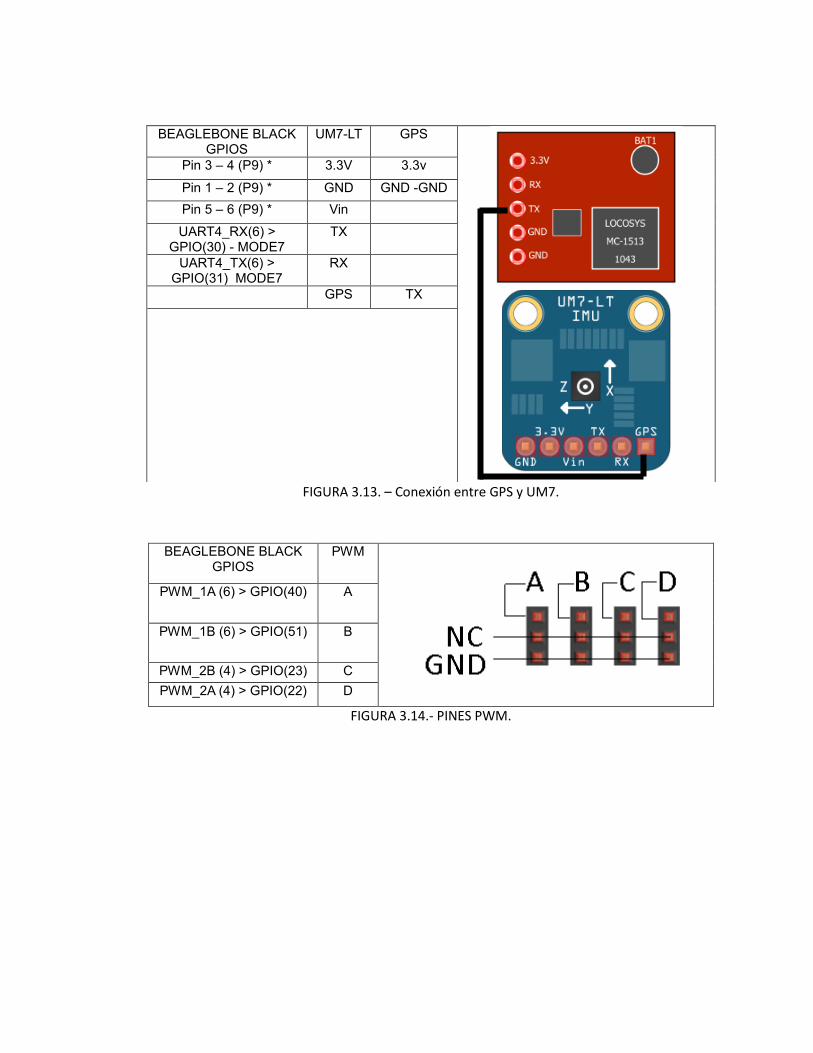
FIGURA 3.13. – Conexión entre GPS y UM7.
FIGURA 3.14.- PINES PWM.
BEAGLEBONE BLACK GPIOS
UM7-LT GPS
Pin 3 – 4 (P9) * 3.3V 3.3v
Pin 1 – 2 (P9) * GND GND -GND
Pin 5 – 6 (P9) * Vin
UART4_RX(6) > GPIO(30) - MODE7
TX
UART4_TX(6) > GPIO(31) MODE7
RX
GPS TX
BEAGLEBONE BLACK GPIOS
PWM
PWM_1A (6) > GPIO(40) A
PWM_1B (6) > GPIO(51) B
PWM_2B (4) > GPIO(23) C
PWM_2A (4) > GPIO(22) D
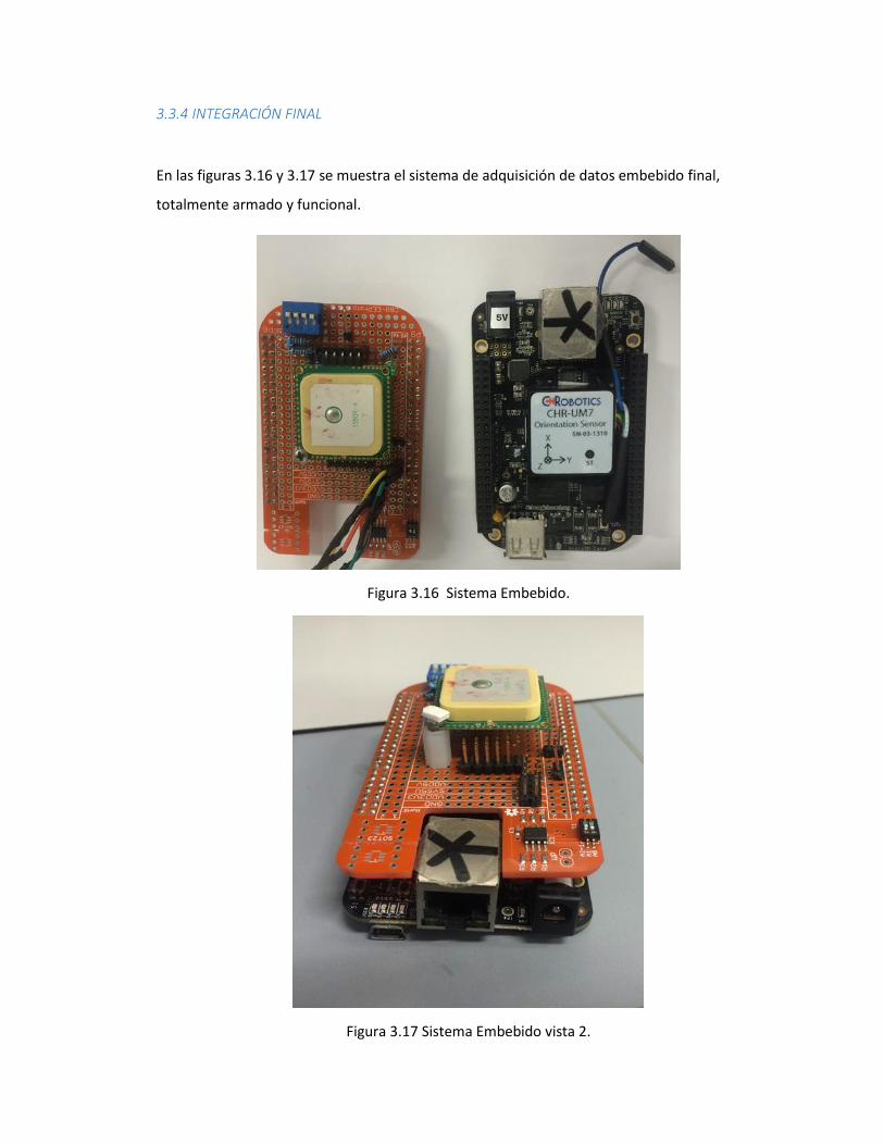
3.3.4 INTEGRACIÓN FINAL
En las figuras 3.16 y 3.17 se muestra el sistema de adquisición de datos embebido final,
totalmente armado y funcional.
Figura 3.16 Sistema Embebido.
Figura 3.17 Sistema Embebido vista 2.
3.4 VALIDACIÓN DE LA PLATAFORMA
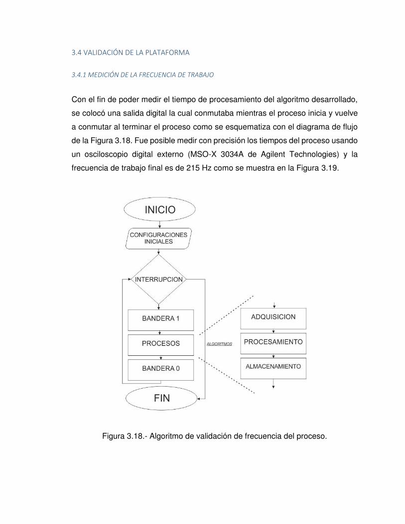
3.4.1 MEDICIÓN DE LA FRECUENCIA DE TRABAJO
Con el fin de poder medir el tiempo de procesamiento del algoritmo desarrollado,
se colocó una salida digital la cual conmutaba mientras el proceso inicia y vuelve
a conmutar al terminar el proceso como se esquematiza con el diagrama de flujo
de la Figura 3.18. Fue posible medir con precisión los tiempos del proceso usando
un osciloscopio digital externo (MSO-X 3034A de Agilent Technologies) y la
frecuencia de trabajo final es de 215 Hz como se muestra en la Figura 3.19.
Figura 3.18.- Algoritmo de validación de frecuencia del proceso.

Figura 3.19 Osciloscopio Aligent Frecuencia del proceso.
3.4.2 INTERFAZ CON MICROAERONAVE
Dentro de la integración para la elaboración de pruebas se utilizó un modelo de
ala fija y se agregó la CV en su interior como se observa en la figura 3.20, cabe
recalcar que además de la computadora se encontraba una batería LIPO que
alimentaba la computadora, el motor y los servomotores del modelo a escala.
Figura 3.20 Avión de ala fija a escala con la CV
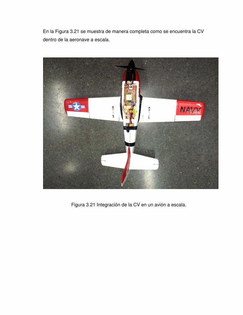
En la Figura 3.21 se muestra de manera completa como se encuentra la CV
dentro de la aeronave a escala.
Figura 3.21 Integración de la CV en un avión a escala.

3.4.3 PRUEBA MECÁNICA EN BANCO DE PRUEBAS
Se realizaron varias pruebas preliminares para comprobar si el sensado de la CV
era coherente tanto en el almacenamiento de datos como en la magnitud y sentido
de las mediciones. Para comprobarlo se diseñaron y construyeron, con ayuda del
M.C. Carlos Antonio Santana Delgado, diferentes rótulas que permiten limitar el
movimiento (hasta un máximo de ±40 grados) en un solo eje independiente, ya
sea alabeo, cabeceo o guiñada. En las Figuras 3.22 y 3.23 se muestran los
diferentes mecanismos en dos diferentes vistas mientras que en el ANEXO 6.7 se
muestran los dibujos de ingeniería finales.
Figura 3.22 Vista superior de las rótulas para alabeo, cabeceo y guiñada.
Figura 3.23 Vista isométrica de las rótulas para alabeo, cabeceo y guiñada.

3.4.3.1 VALIDACIÓN PRELIMINAR EN ALABEO
Se realizó una validación preliminar en alabeo como se muestra en la Figura 3.24
obteniéndose los datos de la Figura 3.25. Se puede concluir que la caracterización
preliminar fue satisfactoria puesto que los datos se guardaron correctamente y la
magnitud de los datos de alabeo fueron los esperados tanto en magnitud como en
sentido. Así mismo, se nota una pequeña interferencia con los datos del cabeceo,
pero esto es atribuible por la construcción física de la rótula que presentaba un
poco de juego mecánico.
Figura 3.24 -. Validación preliminar en alabeo.
Figura 3.25 Resultado de la caracterización preliminar en alabeo.
3.4.3.2 VALIDACIÓN PRELIMINAR EN CABECEO
Al igual que para la validación en alabeo, la validación preliminar en cabeceo fue
exitosa. En las Figuras 3.26 y 3.27 se pueden observar la plataforma de validación
preliminar y los datos de la validación, respectivamente.

Figura 3.26 -. Validación preliminar en cabeceo.
Figura 3.27 Resultado de la caracterización preliminar en cabeceo.
3.4.3.3 VALIDACIÓN PRELIMINAR EN GUIÑADA.
Debido a que los datos de guiñada que arroja el sensor UM7 son filtrados
parcialmente a partir de datos del magnetómetro y que, dentro del laboratorio, el
magnetómetro no funciona adecuadamente por estar en un ambiente cerrado, no
fue posible una validación preliminar en guiñada. Sin embargo, es posible inferir,
a partir de los datos de las validaciones anteriores, que el sistema almacena los
datos correctamente.
3.4.4 VALIDACIÓN DE LA PLATAFORMA CON SISTEMA VICON
La siguiente etapa de experimentación se realizó en el Laboratorio de Navegación
del CIIIA-FIME-UANL que se muestra en la Figura 3.28, este laboratorio cuenta
con un sistema de cámaras infrarrojas, VICON, con el cual es posible obtener la

actitud de un objeto dentro de un área de trabajo determinada. Se utilizó el sistema
de captura de movimiento VICON con el propósito de sensar la actitud del objeto
en alabeo, cabeceo y guiñada.
Figura 3.28 Laboratorio de Navegación
Para esta validación, la CV se fijó dentro de una aeronave a escala en cuyo
exterior se colocaron asimétricamente 5 marcadores reflejantes, necesarios para
capturar el movimiento de la aeronave mediante el sistema VICON. La aeronave
a escala se movió libremente y se registraron los movimientos de alabeo, cabeceo
y guiñada tanto por el sistema VICON como por la CV. La comparación entre estos
registros validó el sistema desarrollado en esta tesis.
Se realizaron una serie de movimientos secuenciales de alabeo, cabeceo y
guiñada y en las Figuras 3.29 ,3.30 y 3.31 respectivamente se muestran las
gráficas de comparación entre los datos por el sistema VICON y la CV.

Figura 3.29 Comparación entre el movimiento de cabeceo por el sistema VICON y la CV.
Figura 3.30 5.15 Comparación entre el movimiento de alabeo por el sistema VICON y la CV.

Figura 3.31 5.15 Comparación entre el movimiento de guiñada por el sistema VICON y la CV.
3.4.5 PRUEBA DE LA PLATAFORMA EN TÚNEL DE VIENTO
Una vez que se pudo determinar que los datos guardados dentro de la CV tienen
un error máximo de ±3 grados, se probó el sistema dentro del túnel de viento del
CIIIA-FIME-UANL; dicho túnel es de trayectoria cerrada, tiene una velocidad
máxima de 60 m/s y una sección de prueba de 1 m x 1m x 1.5 m.
El experimento se realizó a una velocidad de 10 m/s, con el motor encendido y
comandando las superficies de control mediante escalones y dobletes. Una foto
del montaje experimental en túnel de viento se presenta en la Figura 3.32.

Figura 3.32 Sección de prueba del túnel de viento con CV integrada en un Aeroplano
3.4.6 VALIDACIÓN DEL SISTEMA GPS
Para validar el sistema GPS, comprobar su funcionalidad y tener certeza de que
los datos obtenidos son coherentes, se estableció como prueba realizar un
trayecto de un punto inicial a uno final dentro de un automóvil.
Para la representación de estos datos se utilizarán los mapas de
http://www.openstreetmap.org/ los cuales se graficaron con ayuda del software
DIAdem de NATIONAL INSTRUMETS.
El trayecto tuvo una duración de 20 minutos, la distancia recorrida fue de 18.3 km
y finalizó en el CIIIA, cuyas coordenadas son: latitud 25.8642312 y longitud -
100.2466867.
4.- ANALISIS DE RESULTADOS
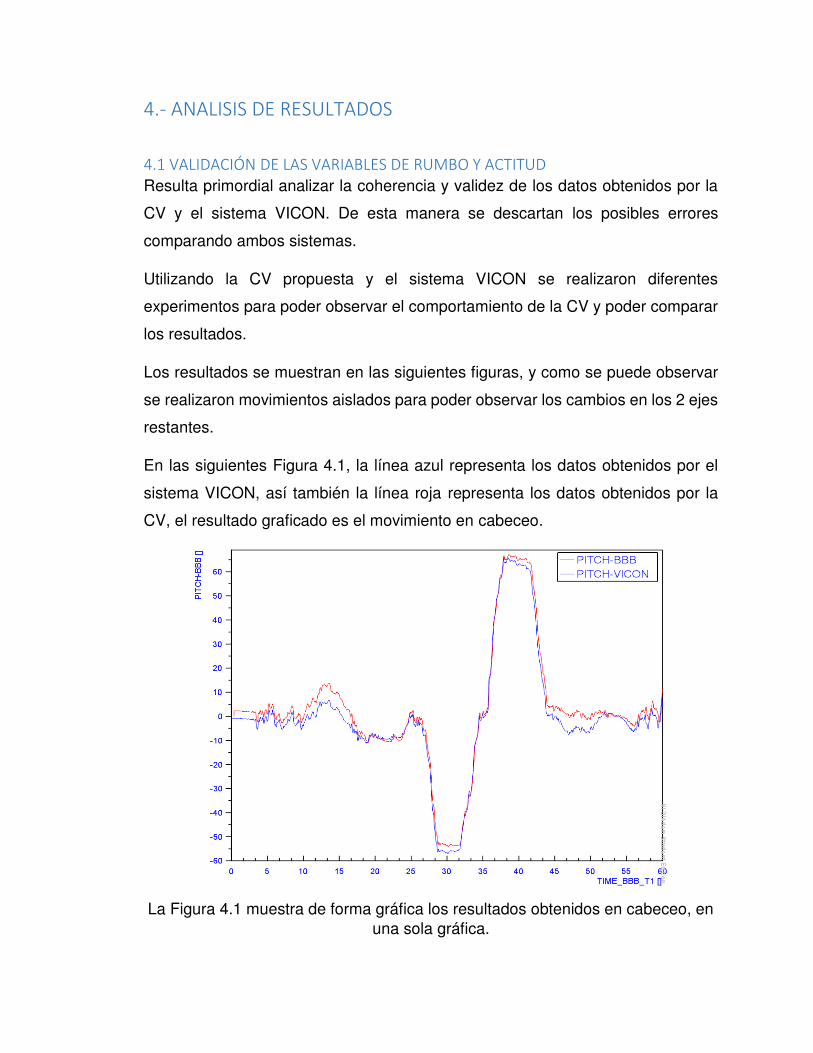
4.1 VALIDACIÓN DE LAS VARIABLES DE RUMBO Y ACTITUD Resulta primordial analizar la coherencia y validez de los datos obtenidos por la
CV y el sistema VICON. De esta manera se descartan los posibles errores
comparando ambos sistemas.
Utilizando la CV propuesta y el sistema VICON se realizaron diferentes
experimentos para poder observar el comportamiento de la CV y poder comparar
los resultados.
Los resultados se muestran en las siguientes figuras, y como se puede observar
se realizaron movimientos aislados para poder observar los cambios en los 2 ejes
restantes.
En las siguientes Figura 4.1, la línea azul representa los datos obtenidos por el
sistema VICON, así también la línea roja representa los datos obtenidos por la
CV, el resultado graficado es el movimiento en cabeceo.
La Figura 4.1 muestra de forma gráfica los resultados obtenidos en cabeceo, en una sola gráfica.

Como se puede observar existe un pequeño desfase de ±3 grados lo cual es
aceptable considerando que no se encuentran alineado el marco del cuerpo de la
CV con respecto al marco del cuerpo de la aeronave.
Por otro lado, en la Figura 4.2, se presentan los resultados graficados para los
movimientos en alabeo.
La Figura 4.2 muestra de forma gráfica los resultados obtenidos en alabeo, en una sola gráfica.
Como se puede observar existe un pequeño desfase de ±2 grados lo cual es
aceptable considerando que no se encuentran alineado el marco del cuerpo de la
CV con respecto al marco del cuerpo de la aeronave.

Los resultados obtenidos en guiñada se muestran en la figura 4.3.
La Figura 4.3 muestra de forma gráfica los resultados obtenidos en guiñada.
Como se puede observar existe una gran diferencia en los datos graficados debido
a que el magnetómetro utilizado se encuentra en relación al norte magnético y
existe una desviación respecto al ángulo de guiñada del laboratorio donde se
encuentra el sistema VICON.

4.2 PRUBAS EN TÚNEL DE VIENTO
El resultado obtenido en la experimentación realizada en el túnel viento están
presentados en la Figura 4.4, Figura 4.5, Figuras 4.6, Figuras 4.7
La Figura 4.4 muestra de forma gráfica los resultados obtenidos del giroscopio en los ejes X, Y, Z.
Como se puede observar en la figura 4.4 cada eje del giroscopio se encuentra
marcado por un color donde el azul es el eje X, rojo es el eje Y así como Z es el
color negro.
En dicha figura se puede observar la oscilación causada por la vibración del motor
cuando se encontraba en funcionamiento, pero el eje que se estaba manipulando
en este caso el eje X nos marca los movimientos registrados por el giroscopio de
manera correcta.

En la figura 4.5 se encuentran registrados los datos obtenidos del acelerómetro.
Como es posible observar el acelerómetro registra las vibraciones causadas por
el motor.
La Figura 4.5 muestra de forma gráfica los resultados obtenidos del Acelerómetro en los ejes X, Y, Z.
En la figura 4.6 se muestran los datos obtenidos por el magnetómetro el cual se
sigue observando las vibraciones provocadas por el motor.
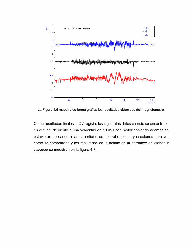
La Figura 4.6 muestra de forma gráfica los resultados obtenidos del magnetómetro.
Como resultados finales la CV registro los siguientes datos cuando se encontraba
en el túnel de viento a una velocidad de 10 m/s con motor enciendo además se
estuvieron aplicando a las superficies de control dobletes y escalones para ver
cómo se comportaba y los resultados de la actitud de la aeronave en alabeo y
cabeceo se muestran en la figura 4.7.

La Figura 4.7 muestra de forma gráfica los resultados obtenidos en alabeo y cabeceo.
Como es posible observar en la figura 4.7 en los resultados obtenidos en los
experimentos es posible notar la vibración de los motores, pero una vez que se
pasa por los filtros correspondientes tiende registrarse mejor la actitud de la
aeronave.
4.3 VALIDACIÓN DEL SISTEMA GPS
Los resultados para validar el GPS se muestran en la figura 4.8 en donde es
marcado el punto inicial, y se marca una trayectoria el cual se siguió con ayuda
de un automóvil hacia a un punto final como se muestra en la figura 4.9.
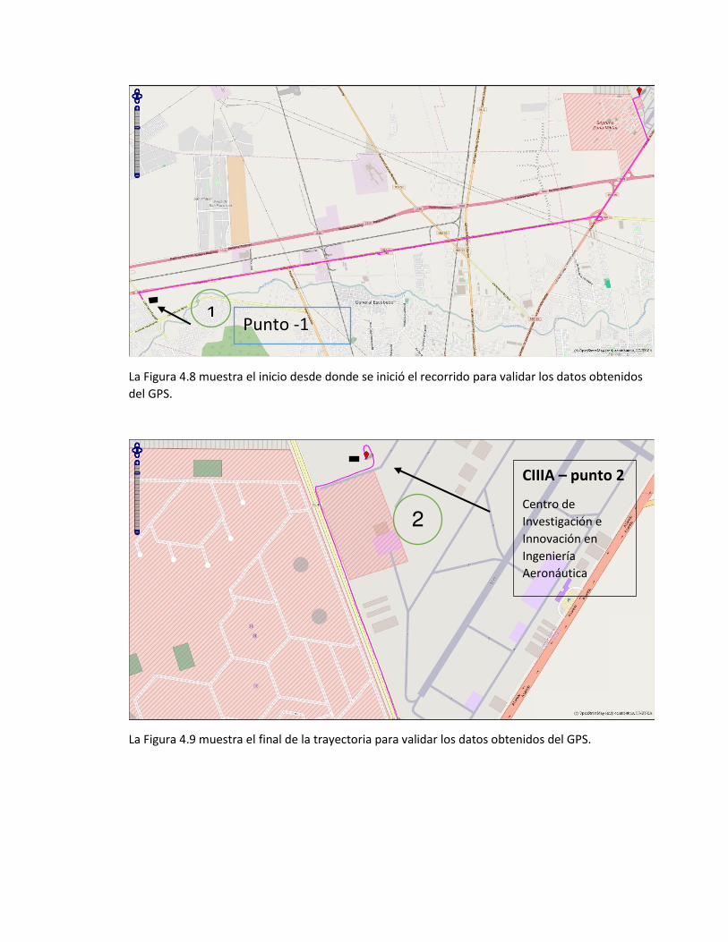
La Figura 4.8 muestra el inicio desde donde se inició el recorrido para validar los datos obtenidos
del GPS.
La Figura 4.9 muestra el final de la trayectoria para validar los datos obtenidos del GPS.
CIIIA – punto 2
Centro de
Investigación e
Innovación en
Ingeniería
Aeronáutica
2
1 Punto -1

Dentro de las gráficas mostradas se representar la trayectoria que se siguió desde
el punto 1 al punto 2. Y se puede observar a simple vista que la ruta trazada
corresponde a la ruta recorrida y no presenta desfases abruptos en la ruta , se
tiene un error máximo de ± 2.5 m.
Por lo tanto, se puede concluir que corresponde la ruta marcado por el GPS con
la ruta recorrida en automóvil.

5.- CONCLUSIÓNES Y RECOCOMENDACIONES
5.1 CONCLUSIONES
Se ha desarrollado un sistema de adquisición de datos cinemáticos que puede ser aplicado a una micro aeronave. El sistema es de bajo costo, pero trabaja satisfactoriamente en tiempo real con sensores COTS a una tasa de trabajo de 215 Hz.
Se han validado el sistema tanto en actitud como en rumbo por medio de comparaciones con datos obtenidos de un sistema de medición de la posición en alta resolución.
El sistema de posicionamiento global ha sido probado satisfactoriamente mediante la comparación entre la ruta seguida y la ruta medida por el sistema.
5.2 TRABAJO A FUTURO
A través de este proyecto se abre la posibilidad de usar esta tecnología para otros fines como puede ser el desarrollo de algoritmos para autopiloto más complejos, pero a partir de este sistema para Vehículos Aéreos No Tripulados.
Los trabajos a futuro se pueden dividir en:
El desarrollo de algoritmos de control e implementación para autopiloto. Integración de barómetros y sensores para cálculo de presión total. Desarrollo de hardware propio donde se integren en una sola placa lo
sensores para poder acercarnos a un tipo COTS. Integración de sistema GPS.

REFERENCIAS
[1] HaiYang Chao, Y. C. (2010). Autopilots for small unmanned aerial vehicles: A survey. International Journal of Control, Automation and Systems, pp 36-44.
[2] David Jackson, A. G. (2005). Evolution of an Avionics System for a High-Altitude UAV. Infotech@Aerospace, Infotech@Aerospace Conferences. Arlington, Virginia: AIAA
[3] Sepehr P. Khaligh, A. M. (2014). A HIL Testbed for Initial Controller Gain Tuning of a Small Unmanned Helicopter. Journal of Intelligent & Robotic Systems, pp 289-308.
[4] Lin, C. E., Hsu, C.-W., Lee, Y.-S., Li, C.-C., Tai, S.-F., & Kang, W.-J. (2004). Verification of Unmanned Air Vehicle Flight Control and Surveillance Using Mobile Communication. Journal of Aerospace Computing, Information, and
Communication, 189-197.
[5] Johnson, E. N., & Schrage, D. P. (2004). System Integration and Operation of a Research Unmanned Aerial Vehicle. Journal of Aerospace Computing,
Information, and Communication, 5-18.
[6] William Pisano, D. L. (2005). Low-Cost UAV Avionics for Autonomous Antenna Calibration. Infotech@Aerospace, Infotech@Aerospace Conferences. Arlington, Virginia: AIAA.
[7] Ilarslan, M., Bayrakceken, M. K., & Arisoy, A. (2011). Avionics System Design of a Mini VTOL UAV. IEEE Aerospace and Electronic Systems Magazine, 35 - 40.
[8] Yu Gu, B. S. (2008). Integrated Avionics System for Research UAVs. AIAA
Guidance, Navigation and Control Conference and Exhibit, Guidance,
Navigation, and Control and Co-located Conferences. Honolulu, Hawaii: AIAA.
[9] Rabah Louali, A. E. (2015). Experimental Approach for Evaluating an UAV COTS-Based Embedded Sensors System. Journal of Intelligent & Robotic
Systems, 1-25.
[10] HaiYang Chao, Y. C. (2010). Autopilots for small unmanned aerial vehicles: A survey. International Journal of Control, Automation and Systems, pp 36-44.
[11] Haiyang Chao, Y. G. (2014). A Survey of Optical Flow Techniques for Robotics Navigation Applications. Journal of Intelligent & Robotic Systems, pp 361-372.

ANEXOS
6.1 ENTORNO DE DESARROLLO
Dentro del Entorno de Desarrollo seleccionado para Programar y desarrollar este
trabajo, ha sido seleccionado Eclipse IDE C/C++ (Ver Figura 6.1).
Este IDE (del inglés: Entornos de desarrollo integrados) es una herramienta de
programación de Código abierto multiplataforma el cual permite trabajar muy
fácilmente con C y C++, así como otros lenguajes de programación, como java,
PHP, PYTHON, JAVASCRIPT, etc.
Dentro de la configuración requerida es necesario contar con las librerías
necesarias para poder hacer una compilación Cruzada.
6.1 Logotipo ECLIPSE
6.1.1 COMPILACION CRUZADA
La compilación cruzada o (Cross Compilation .- inglés ), es un método de
compilación el cual es capaz de crear código ejecutable para una plataforma
distinta en la que se ejecuta el compilador ,por ejemplo si se compila el programa
dentro de una arquitectura x86 o x64 que es lo más común dentro de los
ordenadores , pero directamente no se puede ejecutar en nuestra plataforma
BeagleBone Black debido al tipo de arquitectura el cual es ARM y debido a esta
diferencia es necesario utilizar herramientas de compilación cruzada el cual nos
permitan compilar código para ARM dentro de un x86 o x64.

6.2 INSTALACION DE ECLIPSE IDE DENTRO EN DEBIAN
Para poder instalar Eclipse es necesario abrir un explorador web en un ordenador,
en nuestro caso contamos con un escritorio de Linux debían jessie 8 e ir a la
dirección www.eclipse.org y seleccionar la opción descargas “Downloads” para
descargar el paquete de instalación (ver Figura 6.2).
Figura 6.2 Sección para Descargar Eclipse
Dentro de las variedades de paquetes que existen dentro de eclipse debemos
seleccionar la versión que tiene integración CDT (C/C++ development tooling) ,
por lo tanto la versión a instalar es “Eclipse IDE for C/C++ Developers”, la versión
de eclipse usada en este proceso es LUNA (ver Figura 6.3).
Figura 6.3 Eclipse IDE for C/C++ Developers
Después de haber descargado eclipse, nuestro siguiente paso es mover el archivo a la
raíz usando el comando mv (Ver Figura 6.4)

~/Descargas$ mv eclipse* ~/ // mueve el archivo a la ubicación ~/
~/Descargas$ cd ~/ // ve a la dirección ~/
Figura 6.4 uso del comando “mv”.
Ahora solo queda descomprimir el archivo de eclipse que se encuentra en la raíz
del sistema con el comando tar – xvf (ver Figura 6.5).
~$ tar –xvf eclipse-cpp-mars-2-linux-gtk-x86_64.tar.gz // comando para descomprimir paquetes.
~$ cd eclipse // entra la carpeta eclipse.
~/eclipse$ ./eclipse & // ejecuta el programa eclipse
Figura 6.5 extrayendo paquetes de eclipse.
Hasta este momento ya es posible crear aplicaciones en C/C++ para escritorio
x86 o x64, sin embargo, la plataforma que utilizaremos es en una BeagleBone
Black con una arquitectura ARM, por lo tanto, es necesario configurar eclipse para
una compilación cruzada.
6.3 INSTALACION DE JAVA RUNTIME ENVIROMENT (JRE).
Java Runtime Environment o JRE es un conjunto de utilidades que permite la
ejecución de programas Java, el cual actúa como un intermediario entre sistemas
operativos y Java.
Es necesario instalar JRE (Java Runtime Environment) para el programa eclipse
dependiendo de la versión a utilizar.
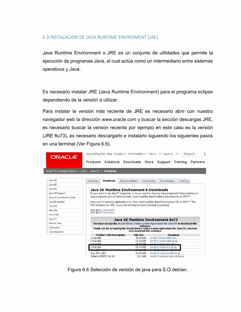
Para instalar la versión más reciente de JRE es necesario abrir con nuestro
navegador web la dirección www.oracle.com y buscar la sección descargas JRE,
es necesario buscar la versión reciente por ejemplo en este caso es la versión
(JRE 8u73), es necesario descargarlo e instalarlo siguiendo los siguientes pasos
en una terminal (Ver Figura 6.6).
Figura 6.6 Selección de versión de java para S.O debían.

Una vez descargado el paquete de instalación de JRE, pasaremos a seguir los
siguientes pasos para instalar y configurar JRE en nuestro ordenador debían
jessie.
1.-Ubicamos y comprobamos en descarga el archivo descargado en nuestro caso
el archivo se llama “jre-8u73-linux-x64.tar.gz” utilizando el comando ls para
mostrar la lista de archivos en esa carpeta.
root@ruben:/home/ruben/Descargas# ls
jre-8u73-linux-x64.tar.gz
2. El siguiente paso es extraer el contenido del archive descargado utilizando el
comando tar zxfv , como se muestra en el siguiente recuadro.
root@ruben:/home/ruben/Descargas# tar zxfv jre-8u73-linux-x64.tar.gz
3. Creamos un nuevo directorio el cual nombraremos java y lo ubicaremos dentro
de la carpeta “usr”, esto es posible utilizando el comando mkdir. [APENDICE B].
root@ruben:/home/ruben/Descargas# mkdir /usr/java
4.Teniendo creada la carpeta “java” en la dirección “/usr/”, se procede a mover el
directorio que fue creado cuando se extrajo el archivo descargado, en este caso
la carpeta o directorio creado se llama “jre1.8.0_73” , utilizando el comando mv
[APENDICE B],se procederá a mover la carpeta.
root@ruben:/home/ruben/Descargas# mv jre1.8.0_73/ /usr/java/
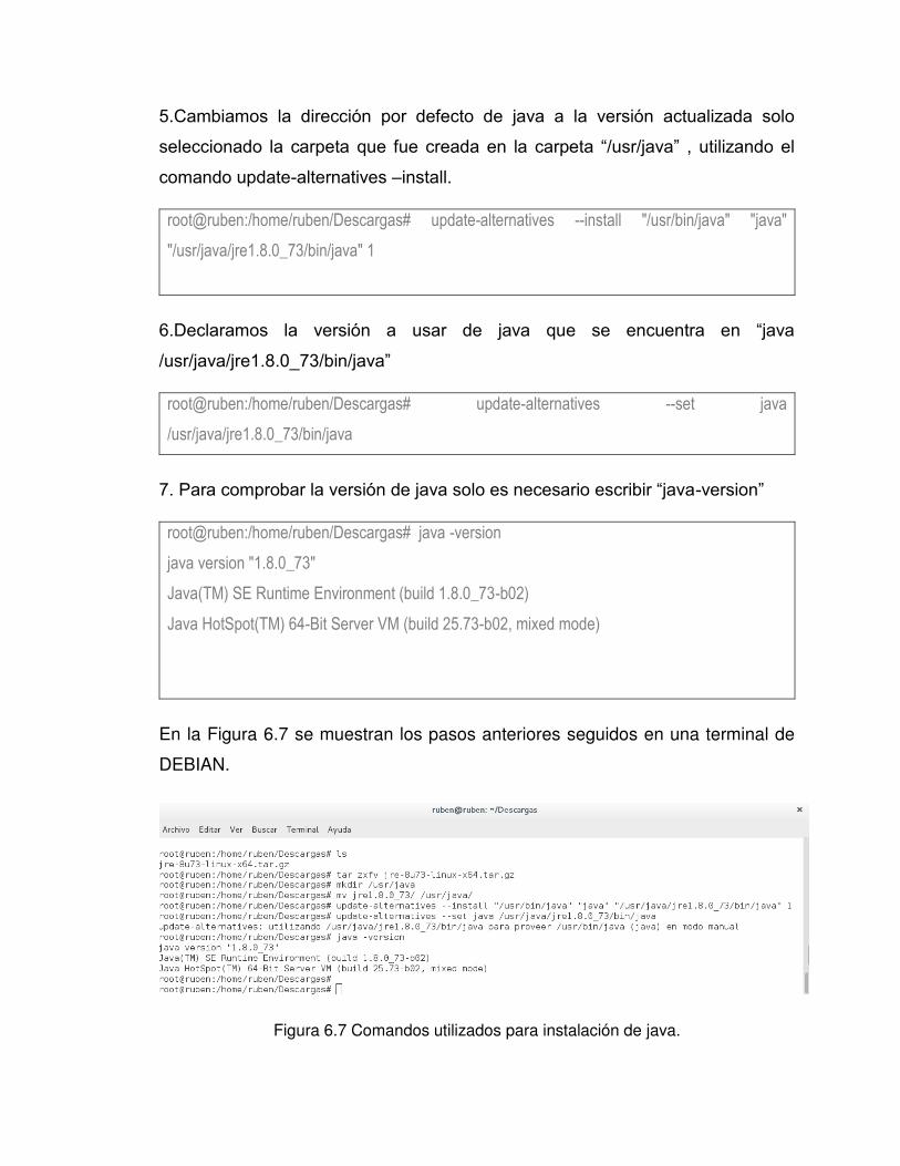
5.Cambiamos la dirección por defecto de java a la versión actualizada solo
seleccionado la carpeta que fue creada en la carpeta “/usr/java” , utilizando el
comando update-alternatives –install.
root@ruben:/home/ruben/Descargas# update-alternatives --install "/usr/bin/java" "java"
"/usr/java/jre1.8.0_73/bin/java" 1
6.Declaramos la versión a usar de java que se encuentra en “java
/usr/java/jre1.8.0_73/bin/java”
root@ruben:/home/ruben/Descargas# update-alternatives --set java
/usr/java/jre1.8.0_73/bin/java
7. Para comprobar la versión de java solo es necesario escribir “java-version”
root@ruben:/home/ruben/Descargas# java -version
java version "1.8.0_73"
Java(TM) SE Runtime Environment (build 1.8.0_73-b02)
Java HotSpot(TM) 64-Bit Server VM (build 25.73-b02, mixed mode)
En la Figura 6.7 se muestran los pasos anteriores seguidos en una terminal de
DEBIAN.
Figura 6.7 Comandos utilizados para instalación de java.
6.4 CONFIGURACION DE ECLIPSE PARA COMPLIACION CRUZADA.
6.4.1 Agregando una arquitectura externa y actualizando sistema.
Antes de configurar eclipse es necesario contar con los paquetes necesarios de
las arquitecturas a enlazar, por lo cual es necesario añadir las arquitecturas
externas o la arquitectura donde se ejecutará el programa a embeber esto con el
fin de emularlo en un PC.
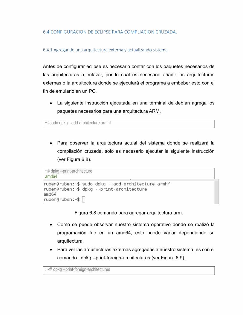
La siguiente instrucción ejecutada en una terminal de debían agrega los
paquetes necesarios para una arquitectura ARM.
~#sudo dpkg --add-architecture armhf
Para observar la arquitectura actual del sistema donde se realizará la
compilación cruzada, solo es necesario ejecutar la siguiente instrucción
(ver Figura 6.8).
~# dpkg --print-architecture amd64
Figura 6.8 comando para agregar arquitectura arm.
Como se puede observar nuestro sistema operativo donde se realizó la
programación fue en un amd64, esto puede variar dependiendo su
arquitectura.
Para ver las arquitecturas externas agregadas a nuestro sistema, es con el
comando : dpkg --print-foreign-architectures (ver Figura 6.9).
:~# dpkg --print-foreign-architectures

Figura 6.9 Comando para ver las arquitecturas disponibles.
Es necesario para este paso hacer una actualización del sistema, utilizando
el comando : sudo apt-get update (Ver Figura 6.10).
:~# sudo apt-get update
Figura 6.10
Los pasos realizados con anterioridad nos permiten agregar una arquitectura
externa y con ella poder emular programas los cuales son creados para otras
arquitecturas en nuestro caso para ser emulados sistemas ARM.
6.4.2 Instalación de herramientas para una compilación cruzada.
En los siguientes pasos se muestras las herramientas necesarias para poder
realizar una compilación cruzada, el paquete build-essential se considera
necesario para a creación de paquetes debian(Ver Figura 6.11).
:~# sudo apt-get install build-essential
Figura 6.11 Instalación de paquetes esenciales para desarrollo de aplicaciones.
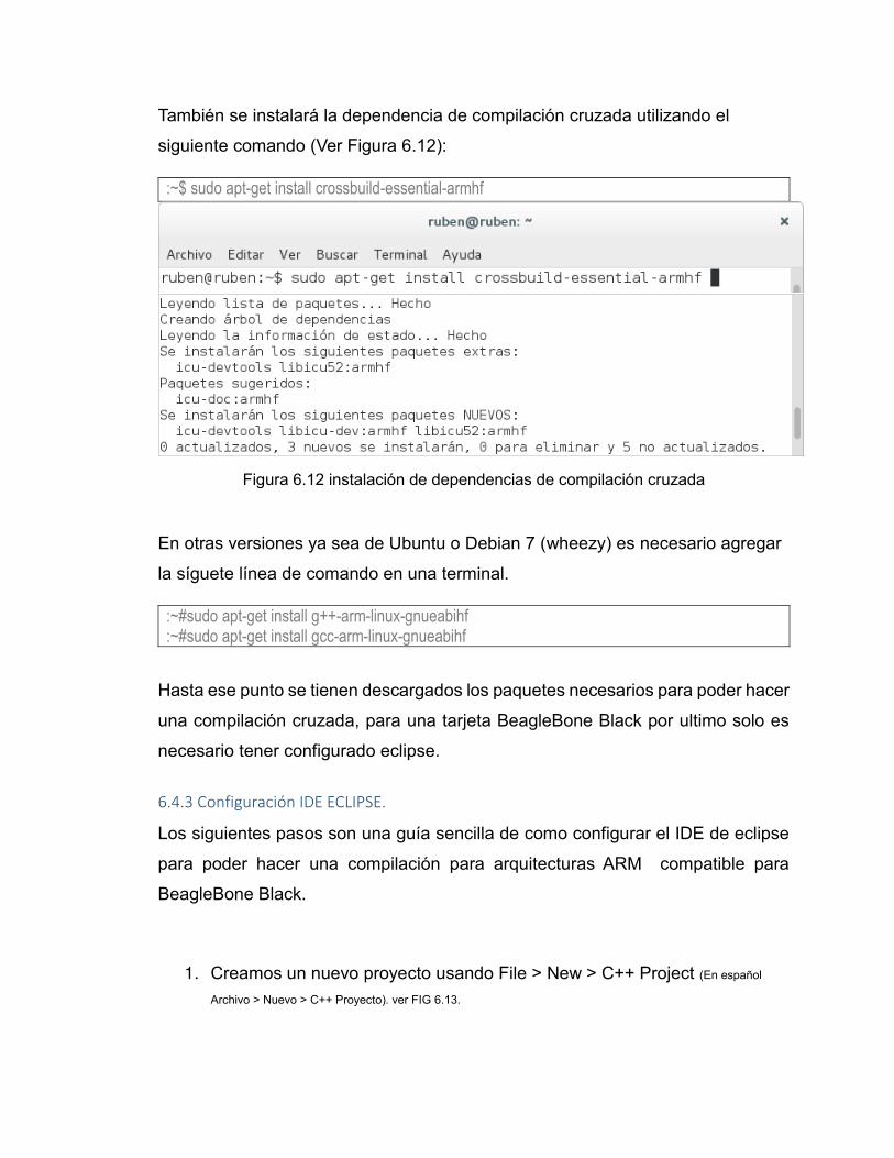
También se instalará la dependencia de compilación cruzada utilizando el
siguiente comando (Ver Figura 6.12):
:~$ sudo apt-get install crossbuild-essential-armhf
Figura 6.12 instalación de dependencias de compilación cruzada
En otras versiones ya sea de Ubuntu o Debian 7 (wheezy) es necesario agregar
la síguete línea de comando en una terminal.
:~#sudo apt-get install g++-arm-linux-gnueabihf :~#sudo apt-get install gcc-arm-linux-gnueabihf
Hasta ese punto se tienen descargados los paquetes necesarios para poder hacer
una compilación cruzada, para una tarjeta BeagleBone Black por ultimo solo es
necesario tener configurado eclipse.
6.4.3 Configuración IDE ECLIPSE.
Los siguientes pasos son una guía sencilla de como configurar el IDE de eclipse
para poder hacer una compilación para arquitecturas ARM compatible para
BeagleBone Black.
1. Creamos un nuevo proyecto usando File > New > C++ Project (En español
Archivo > Nuevo > C++ Proyecto). ver FIG 6.13.

FIG 6.13 Creación de un nuevo proyecto en Eclipse.
2. En la Ventana de C++ Project, Daremos un nombre al proyecto por
ejemplo PruebaBBB , seleccionamos en la opción Project type :
Executable y en toolchains : Cross GCC, después damos clic en Next
para ir a la siguiente sección de configuración. Ver FIG 6.14
FIG 6.14 Ventana de Configuración en plataformas de ejecución.
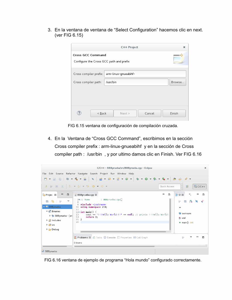
3. En la ventana de ventana de “Select Configuration” hacemos clic en next. (ver FIG 6.15)
FIG 6.15 ventana de configuración de compilación cruzada.
4. En la Ventana de “Cross GCC Command”, escribimos en la sección
Cross compiler prefix : arm-linux-gnueabihf y en la sección de Cross
compiler path : /usr/bin , y por ultimo damos clic en Finish. Ver FIG 6.16
FIG 6.16 ventana de ejemplo de programa “Hola mundo” configurado correctamente.

De esta manera si se requiere hacer un nuevo proyecto con compilación cruzada
es necesario seguir los pasos mencionados anteriormente.
6.5. CONEXIÓN REMOTA A BEAGLEBONE BLACK U“ANDO REMOTE “Y“TEM EXPLORE
El explorador de sistemas remoto (RSE , Remote System Explorer) , es un
conjunto de herramientas para eclipse conocidos como plugins, que permite
conectarse entre el ambiente de eclipse y la tarjeta de desarrollo BeagleBone
Black a través de una conexión , el cual puede ver los archivos remotos que se
encuentras en la tarjeta , transferir archivos entre ambos dispositivos, hacer
búsquedas remotas de archivos , ejecutar comandos y trabajar con los procesos
del sistema remoto.
El sistema RSE puede utilizar el proocolo SSH (Secure SHell, en español:
intérprete de órdenes seguro), con el cual se accede al sistema de la tarjeta
BeagleBone Black.
Para ejecutar RSE en eclipse es necesario seguir los siguientes pasos dentro del
programa eclipse el cual se describen en el siguiente orden:
1. En Eclipse da clic en menú: Window > Show View > Other > Remote
Systems , y damos clic en Ok. (Ver Figura 6.17-a), seguido nos mostrara
la ventana de Remote System (ver Figura 6.17-b).

Fig 6.17 –a “Show View” Fig 6.17 –b “Remote Systems”
Figura 6.17 Configuración de sistemas remotos
2. Damos clic en el icono de Nueva Conexión:
3. En la Ventana de “Remote System Type ” seleccionamos Linux .
4. En la sección de Host Name : ingresamos la dirección IP de la BeagleBone
Black “192.68.7.1” dirección por defecto , en Connection name :
ingresamos el nombre para identificar nuestra BBB “ My BeagleBone
Black” , en Description : “MyBBB” (Ver Figura 6.18).

Figura 6.18 configuración para conexión remota a sistemas Linux.
5. En la Ventana de Files : Configuration , Seleccionamos > ssh.files , y
damos clic en Next (Ver Figura 6.19).
Figura 6.19 Configuración de conexión remota para archivos.
6. En la Ventana de Processes : Configuration > processes.shell.linux , y
damos clic en Next (Ver Figura 6.20).
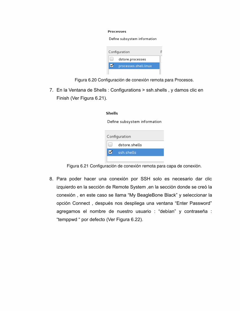
Figura 6.20 Configuración de conexión remota para Procesos.
7. En la Ventana de Shells : Configurations > ssh.shells , y damos clic en
Finish (Ver Figura 6.21).
Figura 6.21 Configuración de conexión remota para capa de conexión.
8. Para poder hacer una conexión por SSH solo es necesario dar clic
izquierdo en la sección de Remote System ,en la sección donde se creó la
conexión , en este caso se llama “My BeagleBone Black” y seleccionar la
opción Connect , después nos despliega una ventana “Enter Password”
agregamos el nombre de nuestro usuario : “debían” y contraseña :
“temppwd “ por defecto (Ver Figura 6.22).

Figura 6.22 Conexión Remota por SSH
El objetivo principal para llevar a cabo la realización de estos pasos, es tener un
sistema en el cual se pueda tener acceso al sistema que se está hospedando en
nuestro caso la tarjeta BeagleBone Black, para tener acceso a los archivos,
sistema y poder ejecutar cualquier comando o programa de forma remota.
6.6 CONFIGURACION DE SENSOR UM7
El Sensor UM7 requiere de ciertas configuraciones para poder transmitir datos y
debido a la gran variedad de datos que puede mostrar, es necesario modificar
ciertas configuraciones como velocidad de comunicación, frecuencia de trabajo,
así como los datos a mostrar, el programa de configuración llamado “CHR serial
Interfaces” es el encargado de realizan las configuraciones mostradas en los
siguientes pasos. El programa “CHR serial Interfaces” es el configurador del UM7 y permite
establecer los datos que saldrán por puerto serial en la Figura 6.23 muestra la
interfaz de configuración.

Figura 5.23 interfaz de UM7.
1. Dentro de las configuraciones de fábrica se establece la velocidad de
comunicación en baudios, que por defecto es 115200 el cual se puede
reconfigurar a cualquier velocidad estándar, en el campo de paridad se
selecciona “None” , y en Stop Bits “1” , dentro de campo port “COM”
seleccionaremos el puerto que nos asigna el sistema este puede varias
desde COM1 hasta cualquier numero imaginable , dependerá de
dispositivos conectados por puerto serial.

2. En la pestaña de “configuration”, dentro de la sección de “Filter Settings”,
los parámetros a modificar dentro de la interfaz son los siguientes Ver
Figura 6.24.
Figura 6.24 configuración de velocidad de conexión
3. Además de modificar la sección “Filter Setting” , se modifica la sección
“Broadcast Rate – NMEA Packets” , donde ,modificaremos los parámetros
“NMEA Sensor Broadcast Rate ” y “NMEA GPS Pose Broadcast Rate” a
valor de 15 (Ver Figura 6.25)
Figura 6.25 configuración de paquetes
115200 54600
Enabled
15
15
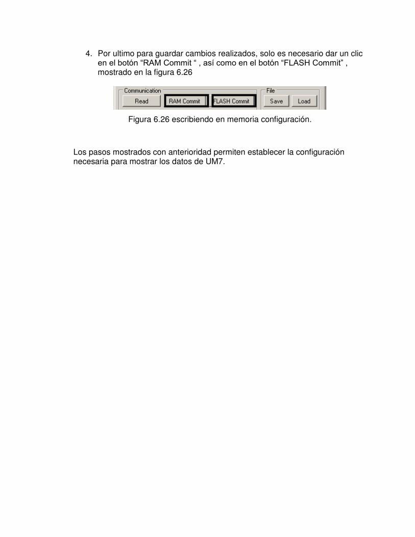
4. Por ultimo para guardar cambios realizados, solo es necesario dar un clic en el botón “RAM Commit “ , así como en el botón “FLASH Commit” , mostrado en la figura 6.26
Figura 6.26 escribiendo en memoria configuración.
Los pasos mostrados con anterioridad permiten establecer la configuración necesaria para mostrar los datos de UM7.
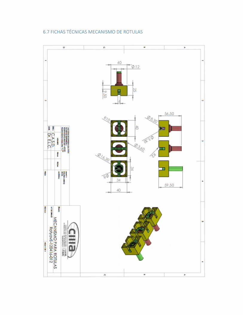
6.7 FICHAS TÉCNICAS MECANISMO DE ROTULAS


APÉNDICE A
1.- CÓDIGO FUENTE MAIN.CPP
/* Inicio de .... MAIN.CPP */ #include "BBBaction.h" #include <stdio.h> #include <stdlib.h> #include <iostream> #include "serialib.h" #include "generate.h" #include "info.h" #include "parser.h" // PortName Uart4 on BeagleBone Black #define DEVICE_PORT "/dev/ttyO4" // GPIOS on BeagleBone Black #define GPIO_LED_GREEN 20 #define GPIO_PIN_A 70 #define GPIO_PIN_B 71 #define GPIO_PIN_C 72 #define GPIO_PIN_D 73 using namespace std; int main() //Se Configurar los GPIO a utilizar asi como el modo de operacion "INPUT - OUTPUT" int DIP_A , DIP_B , DIP_C , DIP_D ; initPin(GPIO_LED_GREEN); setPinDirection(GPIO_LED_GREEN, OUT); initPin(GPIO_PIN_A); setPinDirection(GPIO_PIN_A, IN); initPin(GPIO_PIN_B); setPinDirection(GPIO_PIN_B, IN); // Se se crea un ciclo de espera y muestra el LED GREEN (1-0) en 2 seg intermitente. // El programa avanza cuando el DIP_SWITCH A sea 1 while (DIP_A == 0) DIP_A = getPinValue(GPIO_PIN_A); setPinValue(GPIO_LED_GREEN, ON); sleep(1); setPinValue(GPIO_LED_GREEN, OFF); sleep(1); // Se enciende el LED GREEN , senal de que esta iniciando el sistema. setPinValue(GPIO_LED_GREEN, ON); // La siguiente desgina el nombre del archivo a guardar , asignandole un consecutivo // ejemplo log_num1 -> pasa a log_num2 .. etc. char str[20]; char num[4]; FILE *NuevoArchivo; int pinnum = 0; do pinnum++; sprintf(num,"%i",pinnum); strcpy(str,"log_num"); strcat(str,num); strcat(str,".txt"); NuevoArchivo = fopen(str, "r"); while (NuevoArchivo != NULL); printf("el archivo se guardara con el nombre de : %s\n",str); FILE *fp; fp=fopen(str,"w");

serialib LS; // objeto de la clase Serialib int Ret; // Se utiliza para valores de retorno char Buffer[512]; // Assignacion de tamano de Buffer de serial char buff[2048]; //Assignacion de tamano de buffer de saver. int gen_sz; // Configuracion de Parametros y apertura de Puerto Serial a 115200 baudios. Ret=LS.Open(DEVICE_PORT,115200); // Abriendo Conexion Serial a 115200 Baudios if (Ret!=1) // Si ocurre un error ..... // ... Muestra el mensaje de error de conexion serial.... printf ("Error while opening port. Permission problema ?\n"); return Ret; // ... cierra programa... cout << "Puerto Serial abierto correctamente “; // ... si la conexion se establece envia mensaje ... /*********** Puntadores a estructuras **********/ GlobalINFO info; PARSER parser; zero_INFO (&info); parser_init (&parser); /***********Comprueba si en memoria existe dato actual **********/
//INFO_set_present (&info.present, HEADING_PCHRG); INFO_set_present (&info.present, LATITUDE_PCHRG); INFO_set_present (&info.present, LONGITUDE_PCHRG); INFO_set_present (&info.present, ALTITUDE_PCHRG); INFO_set_present (&info.present, ROLL_PCHRG); INFO_set_present (&info.present, PITCH_PCHRG); INFO_set_present (&info.present, YAW_PCHRG); INFO_set_present (&info.present, GYRO_X); INFO_set_present (&info.present, GYRO_Y); INFO_set_present (&info.present, GYRO_Z); INFO_set_present (&info.present, ACEL_X); INFO_set_present (&info.present, ACEL_Y); INFO_set_present (&info.present, ACEL_Z); INFO_set_present (&info.present, MAGNE_X); INFO_set_present (&info.present, MAGNE_Y); INFO_set_present ( &info.present, MAGNE_Z); do DIP_A = getPinValue(GPIO_PIN_A); zero_INFO(&info); /*********** Actualiza time **********/ parser_init(&parser); /*********** Inicia Analizador **********/ Ret=LS.ReadStringNoTimeOut(Buffer,'\n',512); // Leer un máximo de 512 caracteres // analisis gramatical hasta encontrar "$ y \n \r \0 " parse (&parser, Buffer, (int) strlen(Buffer), &info); // almacenamiento en apuntadores principales. gen_sz = generate_saver(&buff[0], 2048, &info, UM7A1 ); // Generador de codigo tipo nmea en orden pre establecido con chksum. buff[gen_sz] = 0; // printf("%s", &buff[0]); fputs(buff, fp); while (DIP_A == 1); usleep (1000); fclose(fp); //cierra archivo log_num"X".txt cout << "Archivo Salvado"; cout << "Apagando LED GREED OFF"; LS.Close(); cout << "Conexion Cerrada ...."; return 0; /* Fin de .... MAIN.CPP */
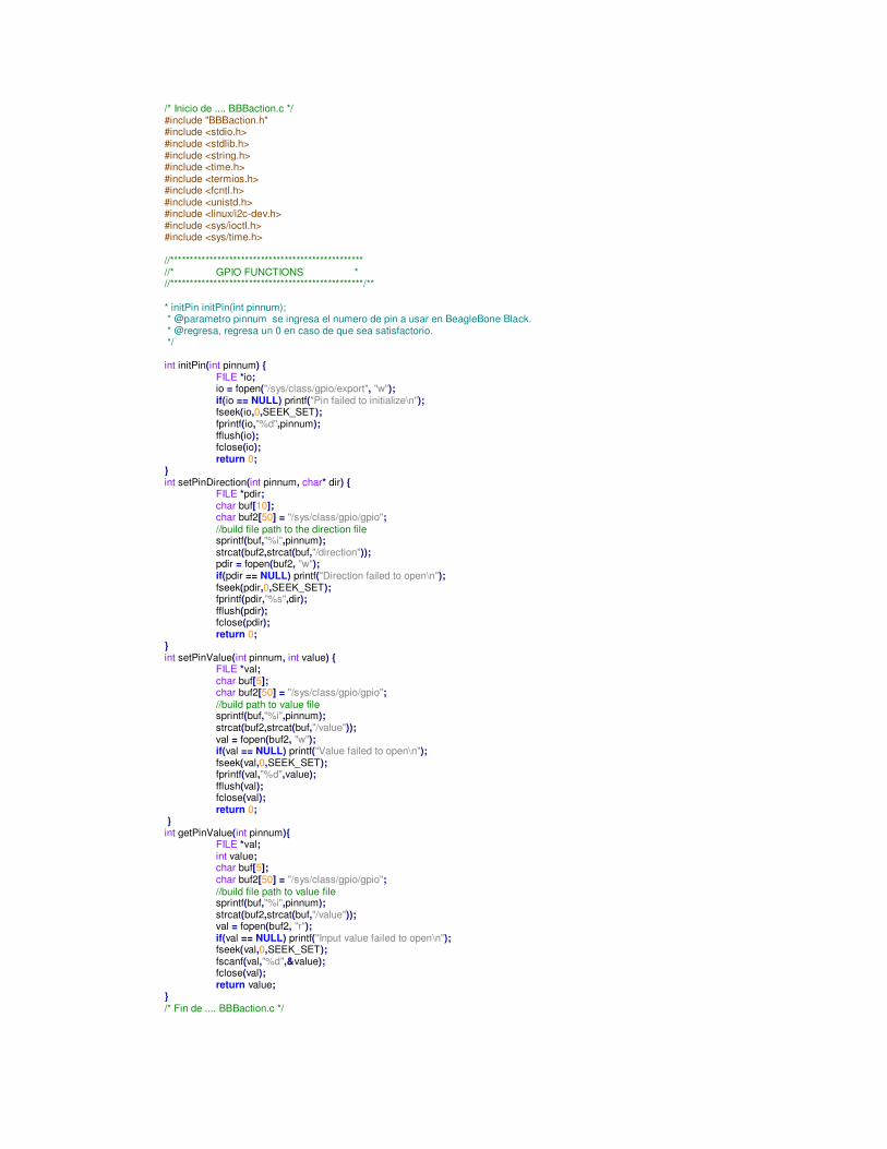
/* Inicio de .... BBBaction.c */ #include "BBBaction.h" #include <stdio.h> #include <stdlib.h> #include <string.h> #include <time.h> #include <termios.h> #include <fcntl.h> #include <unistd.h> #include <linux/i2c-dev.h> #include <sys/ioctl.h> #include <sys/time.h> //************************************************* //* GPIO FUNCTIONS * //*************************************************/** * initPin initPin(int pinnum); * @parametro pinnum se ingresa el numero de pin a usar en BeagleBone Black. * @regresa, regresa un 0 en caso de que sea satisfactorio. */ int initPin(int pinnum) FILE *io; io = fopen("/sys/class/gpio/export", "w"); if(io == NULL) printf("Pin failed to initialize\n"); fseek(io,0,SEEK_SET); fprintf(io,"%d",pinnum); fflush(io); fclose(io); return 0; int setPinDirection(int pinnum, char* dir) FILE *pdir; char buf[10]; char buf2[50] = "/sys/class/gpio/gpio"; //build file path to the direction file sprintf(buf,"%i",pinnum); strcat(buf2,strcat(buf,"/direction")); pdir = fopen(buf2, "w"); if(pdir == NULL) printf("Direction failed to open\n"); fseek(pdir,0,SEEK_SET); fprintf(pdir,"%s",dir); fflush(pdir); fclose(pdir); return 0; int setPinValue(int pinnum, int value) FILE *val; char buf[5]; char buf2[50] = "/sys/class/gpio/gpio"; //build path to value file sprintf(buf,"%i",pinnum); strcat(buf2,strcat(buf,"/value")); val = fopen(buf2, "w"); if(val == NULL) printf("Value failed to open\n"); fseek(val,0,SEEK_SET); fprintf(val,"%d",value); fflush(val); fclose(val); return 0; int getPinValue(int pinnum) FILE *val; int value; char buf[5]; char buf2[50] = "/sys/class/gpio/gpio"; //build file path to value file sprintf(buf,"%i",pinnum); strcat(buf2,strcat(buf,"/value")); val = fopen(buf2, "r"); if(val == NULL) printf("Input value failed to open\n"); fseek(val,0,SEEK_SET); fscanf(val,"%d",&value); fclose(val); return value; /* Fin de .... BBBaction.c */

/* Inicio de .... BBBaction.h */ /* * BBBactoin.h * * Created on: 23/05/2016 * Author: ruben */ #ifndef BBBACTION_H_ #define BBBACTION_H_ #include "info.h" #include "sentence.h" #include <stdio.h> #include <stdlib.h> #include <string.h> #include <time.h> #include <termios.h> #include <fcntl.h> #include <unistd.h> #include <linux/i2c-dev.h> #include <sys/ioctl.h> #include <sys/time.h> //Definitions #define OUT "out" #define IN "in" #define ON1 #define OFF 0 //GPIO Prototypes int initPin(int pinnum); int setPinDirection(int pinnum, char* dir); int setPinValue(int pinnum, int value); int getPinValue(int pinnum); #endif /* BBBACTION_H_ */ /* Fin de .... BBBaction.h */

/* Inicio de .... context.c */ #include "context.h" #include <stdarg.h> #include <stdio.h> typedef struct _nmeaPROPERTY nmeaTraceFunc trace_func; //< la funcion de raestreo por defecto es NULL (desactivado)// nmeaErrorFunc error_func; //< la función de error , por defecto es NULL (desactivado ) / int parse_buff_size; //<el tamaño a utilizar para buffers temporales , mínimo es NMEA_MIN_PARSEBUFF // nmeaPROPERTY; static nmeaPROPERTY property = .trace_func = NULL, .error_func = NULL, .parse_buff_size = NMEA_DEF_PARSEBUFF ; // Establecer la función de rastreo void context_set_trace_func(nmeaTraceFunc func) property.trace_func = func; //// //Set the error function // // @Parametro de entrada a la funcion de error. void context_set_error_func(nmeaErrorFunc func) property.error_func = func; /// Ajuste el tamaño de búfer para buffers temporales . // Si el tamaño es menor que NMEA_MIN_PARSEBUFF , a continuación, el tamaño que se // Configurado será NMEA_MIN_PARSEBUFF . // @param Buff_size el tamaño del búfer de buffers temporales void context_set_buffer_size(int buff_size) if (buff_size < NMEA_MIN_PARSEBUFF) property.parse_buff_size = NMEA_MIN_PARSEBUFF; else property.parse_buff_size = buff_size; // @regresa el tamano del buffer y buffers temporales. // int context_get_buffer_size(void) return property.parse_buff_size; /** crea una cadena con formato * @parametro str es cadena con formato. */ void trace(const char *str, ...) nmeaTraceFunc func = property.trace_func; if (func) int size; va_list arg_list; char buff[property.parse_buff_size]; va_start(arg_list, str); size = vsnprintf(&buff[0], property.parse_buff_size - 1, str, arg_list); va_end(arg_list); if (size > 0) (*func)(&buff[0], size); void trace_buff(const char *buff, int buff_size) nmeaTraceFunc func = property.trace_func; if (func && buff_size) (*func)(buff, buff_size); void error(const char *str, ...) nmeaErrorFunc func = property.error_func; if (func) int size; va_list arg_list; char buff[property.parse_buff_size]; va_start(arg_list, str); size = vsnprintf(&buff[0], property.parse_buff_size - 1, str, arg_list); va_end(arg_list); if (size > 0) (*func)(&buff[0], size); /* Fin de .... context.c */

/* Inicio de .... context.h */ #ifndef CONTEXT_H__ #define CONTEXT_H__ /** dimencion de buffers temporal y por defect */ #define NMEA_DEF_PARSEBUFF 1024 #define NMEA_MIN_PARSEBUFF 256 /** * funcion de tipo definicion por seguimiento. * @parametro str cadena para seguimiento * @parametro str_size longitud o tamano de la cadena. */ typedef void (*nmeaTraceFunc)(const char *str, int str_size); /** * Funcion de tipo , definicion de registro de errores. * * @parametro str cadena a almacenar registro de error (log) * @parametro str_size longiud de la cadena (str) * */ typedef void (*nmeaErrorFunc)(const char *str, int str_size); void context_set_trace_func(nmeaTraceFunc func); void context_set_error_func(nmeaErrorFunc func); void context_set_buffer_size(int buff_size); int context_get_buffer_size(void); void trace(const char *str, ...) __attribute__ ((format(printf, 1, 2))); void trace_buff(const char *buff, int buff_size); void error(const char *str, ...) __attribute__ ((format(printf, 1, 2))); #endif /* CONTEXT_H__ */ /* Inicio de .... context.h */
/* Inicio de .... conversions.c */ #include "conversions.h" #include "gmath.h" #include <assert.h> #include <string.h> #include <math.h> /* Llena la estructura normaPCHRP desde la estructura de paquetes GlobalINFO * @parametro pack un puntero a la estructura de paquetes * @parametro info un puntero a la estructura GlobalINFO */ void PCHRP2info(const normaPCHRP *pack, GlobalINFO *info) assert(pack); assert(info); info->present |= pack->present; INFO_set_present(&info->present, SMASK); info->smask |= PCHRP; if (INFO_is_present(pack->present, UTCTIME)) info->utc.hour = pack->utc.hour; info->utc.min = pack->utc.min; info->utc.sec = pack->utc.sec; info->utc.hsec = pack->utc.hsec; info->pe_pchrp = pack->pe_pchrp; info->pn_pchrp = pack->pn_pchrp; info->alt_pchrp = pack->alt_pchrp; info->roll_pchrp = pack->roll_pchrp; info->pitch_pchrp = pack->pitch_pchrp; info->yaw_pchrp = pack->yaw_pchrp; info->heading_pchrp = pack->heading_pchrp; /** Llena la estructura nmeaPCHRH desde la estructura de paquetes GlobalINFO * @parametro pack un puntero a la estructura de paquetes * @parametro info un puntero a la estructura GlobalINFO */ void PCHRH2info(const normaPCHRH *pack, GlobalINFO *info) assert(pack); assert(info); info->present |= pack->present; INFO_set_present(&info->present, SMASK); info->smask |= PCHRH; if (INFO_is_present(pack->present, UTCTIME)) info->utc.hour = pack->utc.hour; info->utc.min = pack->utc.min; info->utc.sec = pack->utc.sec; info->utc.hsec = pack->utc.hsec; info->ACCEL_PCHRH = pack->ACCEL_PCHRH; info->GYRO_PCHRH = pack->GYRO_PCHRH; info->MAG_PCHRH = pack->MAG_PCHRH; info->GPS_PCHRH = pack->GPS_PCHRH; info->res1_PCHRH = pack->res1_PCHRH; info->res2_PCHRH = pack->res2_PCHRH; info->res3_PCHRH = pack->res3_PCHRH;
/* Llena la estructura nmeaPCHRA desde la estructura de paquetes GlobalINFO * @parametro pack un puntero a la estructura de paquetes * @parametro info un puntero a la estructura GlobalINFO */ void PCHRA2info(const normaPCHRA *pack, GlobalINFO *info) assert(pack); assert(info); info->present |= pack->present; INFO_set_present(&info->present, SMASK); info->smask |= PCHRA; if (INFO_is_present(pack->present, UTCTIME)) info->utc.hour = pack->utc.hour; info->utc.min = pack->utc.min; info->utc.sec = pack->utc.sec; info->utc.hsec = pack->utc.hsec; info->roll_pchra = pack->roll_pchra; info->pitch_pchra = pack->pitch_pchra; info->yaw_pchra = pack->yaw_pchra; info->heading_pchra = pack->heading_pchra;
/** * Llena la estructura nmeaPCHRS desde la estructura de paquetes GlobalINFO * @parametro pack un puntero a la estructura de paquetes * @parametro info un puntero a la estructura GlobalINFO */ void PCHRS2info(const normaPCHRS *pack, GlobalINFO *info) assert(pack); assert(info); int control_sensor = pack->count_pchrs; info->present |= pack->present; INFO_set_present(&info->present, SMASK); info->smask |= PCHRS; if (INFO_is_present(pack->present, UTCTIME)) info->utc.hour = pack->utc.hour; info->utc.min = pack->utc.min; info->utc.sec = pack->utc.sec; info->utc.hsec = pack->utc.hsec; /* @parametro control_sensor define giroscopio [0] acelerometro [1] y magnetometro [2]. */ if (control_sensor == 0) info->sensor_x_gyro = pack->sensor_x_pchrs; info->sensor_y_gyro = pack->sensor_y_pchrs; info->sensor_z_gyro = pack->sensor_z_pchrs; if (control_sensor == 1 ) info->sensor_x_acel = pack->sensor_x_pchrs; info->sensor_y_acel = pack->sensor_y_pchrs; info->sensor_z_acel = pack->sensor_z_pchrs; if (control_sensor == 2) info->sensor_x_magnet = pack->sensor_x_pchrs; info->sensor_y_magnet = pack->sensor_y_pchrs; info->sensor_z_magnet = pack->sensor_z_pchrs; /* info->count_pchrs = pack->count_pchrs; info->sensor_x_pchrs = pack->sensor_x_pchrs; info->sensor_y_pchrs = pack->sensor_y_pchrs; info->sensor_z_pchrs = pack->sensor_z_pchrs; */ /* Llena la estructura nmeaPCHRR desde la estructura de paquetes GlobalINFO * @parametro pack un puntero a la estructura de paquetes * @parametro info un puntero a la estructura GlobalINFO */ void PCHRR2info(const normaPCHRR *pack, GlobalINFO *info) assert(pack); assert(info); info->present |= pack->present; INFO_set_present(&info->present, SMASK); info->smask |= PCHRR; if (INFO_is_present(pack->present, UTCTIME)) info->utc.hour = pack->utc.hour; info->utc.min = pack->utc.min; info->utc.sec = pack->utc.sec; info->utc.hsec = pack->utc.hsec; info->vn_pchrr = pack->vn_pchrr; info->ve_pchrr = pack->ve_pchrr; info->vu_pchrr = pack->vu_pchrr; info->roll_pchrr = pack->roll_pchrr; info->pitch_pchrr = pack->pitch_pchrr; info->yaw_pchrr = pack->yaw_pchrr;
/* Llena la estructura nmeaPCHRG desde la estructura de paquetes GlobalINFO * @parametro pack un puntero a la estructura de paquetes * @parametro info un puntero a la estructura GlobalINFO */ void PCHRG2info(const normaPCHRG *pack, GlobalINFO *info) assert(pack); assert(info); info->present |= pack->present; INFO_set_present(&info->present, SMASK); info->smask |= PCHRG; if (INFO_is_present(pack->present, UTCTIME)) info->utc.hour = pack->utc.hour; info->utc.min = pack->utc.min; info->utc.sec = pack->utc.sec; info->utc.hsec = pack->utc.hsec; info->latitude_pchrg = pack->latitude_pchrg; info->longitude_pchrg = pack->longitude_pchrg; info->altitude_pchrg = pack->altitude_pchrg; info->roll_pchrg = pack->roll_pchrg; info->pitch_pchrg = pack->pitch_pchrg; info->yaw_pchrg = pack->yaw_pchrg; info->heading_pchrg = pack->heading_pchrg; /* Llena la estructura nmeaPCHRQ desde la estructura de paquetes GlobalINFO * @parametro pack un puntero a la estructura de paquetes * @parametro info un puntero a la estructura GlobalINFO */ void PCHRQ2info(const normaPCHRQ *pack, GlobalINFO *info) assert(pack); assert(info); info->present |= pack->present; INFO_set_present(&info->present, SMASK); info->smask |= PCHRQ; if (INFO_is_present(pack->present, UTCTIME)) info->utc.hour = pack->utc.hour; info->utc.min = pack->utc.min; info->utc.sec = pack->utc.sec; info->utc.hsec = pack->utc.hsec; info->a_pchrq = pack->a_pchrq; info->b_pchrq = pack->b_pchrq; info->b_pchrq = pack->c_pchrq; info->d_pchrq = pack->d_pchrq; /** * Convierte una estructura GlobalINFO en una estructura normaPCHRG * @parametro info , un puntero a la estructura GlobalINFO * @parametro pack , un puntero a la estructura normaPCHRG */ void info2PCHRG(const GlobalINFO *info, normaPCHRG *pack) assert(pack); assert(info); zero_PCHRG(pack); pack->present = info->present; INFO_unset_present(&pack->present, SMASK); if (INFO_is_present(info->present, UTCDATE)) pack->utc.year = info->utc.year; pack->utc.mon = info->utc.mon; pack->utc.day = info->utc.day; if (INFO_is_present(info->present, UTCTIME)) pack->utc.hour = info->utc.hour; pack->utc.min = info->utc.min; pack->utc.sec = info->utc.sec; pack->utc.hsec = info->utc.hsec;

if (INFO_is_present(info->present, LATITUDE_PCHRG)) pack->latitude_pchrg = info->latitude_pchrg ; if (INFO_is_present(info->present, LONGITUDE_PCHRG)) pack->longitude_pchrg = info->longitude_pchrg; if (INFO_is_present(info->present, ALTITUDE_PCHRG)) pack->altitude_pchrg = info->altitude_pchrg; if (INFO_is_present(info->present, ROLL_PCHRG)) pack->roll_pchrg = info->roll_pchrg; if (INFO_is_present(info->present, PITCH_PCHRG)) pack->pitch_pchrg = info->pitch_pchrg; if (INFO_is_present(info->present, YAW_PCHRG)) pack->yaw_pchrg = info->yaw_pchrg; /* if (nmea_INFO_is_present(info->present, HEADING_PCHRG)) pack->heading_pchrg = info->heading_pchrg; */ /** Convierte una estructura bbbUM7A1en una estructura GlobalINFO * @parametro info , un puntero a la estructura GlobalINFO * @parametro pack , un puntero a la estructura bbbUM7A1 */ void info2UM7A1(const GlobalINFO *info, bbbUM7A1 *pack) assert(pack); assert(info); zero_UM7A1(pack); pack->present = info->present; INFO_unset_present(&pack->present, SMASK); if (INFO_is_present(info->present, UTCDATE)) pack->utc.year = info->utc.year; pack->utc.mon = info->utc.mon; pack->utc.day = info->utc.day; if (INFO_is_present(info->present, UTCTIME)) pack->utc.hour = info->utc.hour; pack->utc.min = info->utc.min; pack->utc.sec = info->utc.sec; pack->utc.hsec = info->utc.hsec; if (INFO_is_present(info->present, LATITUDE_PCHRG)) pack->latitude_pchrg = info->latitude_pchrg ; if (INFO_is_present(info->present, LONGITUDE_PCHRG)) pack->longitude_pchrg = info->longitude_pchrg; if (INFO_is_present(info->present, ALTITUDE_PCHRG)) pack->altitude_pchrg = info->altitude_pchrg; if (INFO_is_present(info->present, ROLL_PCHRG)) pack->roll_pchrg = info->roll_pchrg; if (INFO_is_present(info->present, PITCH_PCHRG)) pack->pitch_pchrg = info->pitch_pchrg; if (INFO_is_present(info->present, YAW_PCHRG)) pack->yaw_pchrg = info->yaw_pchrg; if (INFO_is_present(info->present, GYRO_X)) pack->sensor_x_gyro = info->sensor_x_gyro; if (INFO_is_present(info->present, GYRO_Y)) pack->sensor_y_gyro = info->sensor_y_gyro; if (INFO_is_present(info->present, GYRO_Z)) pack->sensor_z_gyro = info->sensor_z_gyro; if (INFO_is_present(info->present, ACEL_X)) pack->sensor_x_acel = info->sensor_x_acel; if (INFO_is_present(info->present, ACEL_Y)) pack->sensor_y_acel = info->sensor_y_acel; if (INFO_is_present(info->present, ACEL_Z)) pack->sensor_z_acel = info->sensor_z_acel;

if (INFO_is_present(info->present, MAGNE_X)) pack->sensor_x_magnet = info->sensor_x_magnet; if (INFO_is_present(info->present, MAGNE_Y)) pack->sensor_y_magnet = info->sensor_y_magnet; if (INFO_is_present(info->present, MAGNE_Z)) pack->sensor_z_magnet = info->sensor_z_magnet; /* if (nmea_INFO_is_present(info->present, HEADING_PCHRG)) pack->heading_pchrg = info->heading_pchrg; */ /* fin de .... conversions.c */
/* Inicio de .... conversions.h */ #ifndef CONVERSIONS_H__ #define CONVERSIONS_H__ #include "sentence.h" #include "info.h" //int nmea_gsv_npack(int sat_count); void info2UM7A1(const GlobalINFO *info, bbbUM7A1 *pack); void info2PCHRG(const GlobalINFO *info, normaPCHRG *pack); /*------------------------------------------------------*/ void PCHRP2info(const normaPCHRP *pack, GlobalINFO *info); void PCHRH2info(const normaPCHRH *pack, GlobalINFO *info); void PCHRA2info(const normaPCHRA *pack, GlobalINFO *info); void PCHRS2info(const normaPCHRS *pack, GlobalINFO *info); void PCHRR2info(const normaPCHRR *pack, GlobalINFO *info); void PCHRG2info(const normaPCHRG *pack, GlobalINFO *info); void PCHRQ2info(const normaPCHRQ *pack, GlobalINFO *info);
#endif /* CONVERSIONS_H__ */ /* Fin de .... conversions.c */

/* Inicio de .... generate.c */ #include "generate.h" #include "tok.h" #include "conversions.h" #include <stdio.h> #include <stdbool.h> /** * Generate a PCHRG sentence from an normaGPRMC structure * @param s a pointer to the buffer to generate the string in * @param len the size of the buffer * @param pack the structure * @return the length of the generated sentence */ int generator_PCHRG(char *s, const int len, const normaPCHRG *pack) char sTime[16]; char sDate[16]; char slatitude_pchrg[16]; char slongitude_pchrg[16]; char saltitude_pchrg[16]; char sroll_pchrg[16]; char spitch_pchrg[16]; char syaw_pchrg[16]; char sheading_pchrg[16]; slatitude_pchrg[0]; slongitude_pchrg[0]; saltitude_pchrg[0]; sroll_pchrg[0]; spitch_pchrg[0]; syaw_pchrg[0]; sheading_pchrg[0]; if (INFO_is_present(pack->present, UTCDATE)) snprintf(&sDate[0], sizeof(sDate), "%02d%02d%02d", pack->utc.day, pack->utc.mon + 1, pack->utc.year - 100); if (INFO_is_present(pack->present, UTCTIME)) snprintf(&sTime[0], sizeof(sTime), "%02d%02d%02d.%02d", pack->utc.hour, pack->utc.min, pack->utc.sec, pack->utc.hsec); if (INFO_is_present(pack->present, LATITUDE_PCHRG)) snprintf(&slatitude_pchrg[0], sizeof(slatitude_pchrg), "%09.6f", pack->latitude_pchrg); if (INFO_is_present(pack->present, LONGITUDE_PCHRG)) snprintf(&slongitude_pchrg[0], sizeof(slongitude_pchrg), "%010.5f", pack->longitude_pchrg); if (INFO_is_present(pack->present, ALTITUDE_PCHRG )) snprintf(&saltitude_pchrg[0], sizeof(saltitude_pchrg), "%03.0f", pack->altitude_pchrg); if (INFO_is_present(pack->present, ROLL_PCHRG)) snprintf(&sroll_pchrg[0], sizeof(sroll_pchrg), "%3.16f", pack->roll_pchrg); if (INFO_is_present(pack->present, PITCH_PCHRG)) snprintf(&spitch_pchrg[0], sizeof(spitch_pchrg), "%3.16f", pack->pitch_pchrg); if (INFO_is_present(pack->present, YAW_PCHRG)) snprintf(&syaw_pchrg[0], sizeof(syaw_pchrg), "%f", pack->yaw_pchrg); /* if (nmea_INFO_is_present(pack->present, HEADING_PCHRG)) snprintf(&sheading_pchrg[0], sizeof(sheading_pchrg), "%f", pack->heading_pchrg); */
return norma_printf(s, len, "$PCHRG,%s,%s,%s,%s,%s,%s,%s,%s", &sTime[0] , &slatitude_pchrg[0], &slongitude_pchrg[0],&saltitude_pchrg[0], &sroll_pchrg[0],
&spitch_pchrg[0], &syaw_pchrg[0], &sheading_pchrg[0]);

/* Generate a UM7A1 sentence from an bbbUM7A1 structure * @param s a pointer to the buffer to generate the string in * @param len the size of the buffer * @param pack the structure * @return the length of the generated sentence */ int generator_UM7A1(char *s, const int len, const bbbUM7A1 *pack) char sTime[16] , sDate[16] , Ssensor_x_gyro[16] , Ssensor_y_gyro[16]; char Ssensor_z_gyro[16] , Ssensor_x_acel[16] , Ssensor_y_acel[16]; char Ssensor_z_acel[16] , Ssensor_x_magnet[16] , Ssensor_y_magnet[16]; char Ssensor_z_magnet[16] , slatitude_pchrg[16] , slongitude_pchrg[16]; char saltitude_pchrg[16] , sroll_pchrg[16] , spitch_pchrg[16]; char syaw_pchrg[16] , sheading_pchrg[16]; Ssensor_x_gyro[0] , Ssensor_y_gyro[0] , Ssensor_z_gyro[0] , Ssensor_x_acel[0]; Ssensor_y_acel[0] , Ssensor_z_acel[0] , Ssensor_x_magnet[0] ,Ssensor_y_magnet[0]; Ssensor_z_magnet[0], slatitude_pchrg[0] , slongitude_pchrg[0] , saltitude_pchrg[0]; sroll_pchrg[0] , spitch_pchrg[0] , syaw_pchrg[0] , sheading_pchrg[0]; if (INFO_is_present(pack->present, UTCTIME)) snprintf(&sTime[0], sizeof(sTime), "%02d:%02d:%02d.%03d", pack->utc.hour, pack->utc.min, pack->utc.sec, pack->utc.hsec); if (INFO_is_present(pack->present, LATITUDE_PCHRG)) snprintf(&slatitude_pchrg[0], sizeof(slatitude_pchrg), "%09.6f", pack->latitude_pchrg); if (INFO_is_present(pack->present, LONGITUDE_PCHRG)) snprintf(&slongitude_pchrg[0], sizeof(slongitude_pchrg), "%010.6f", pack->longitude_pchrg); if (INFO_is_present(pack->present, ALTITUDE_PCHRG )) snprintf(&saltitude_pchrg[0], sizeof(saltitude_pchrg), "%03.3f", pack->altitude_pchrg); if (INFO_is_present(pack->present, ROLL_PCHRG)) snprintf(&sroll_pchrg[0], sizeof(sroll_pchrg), "%3.5f", pack->roll_pchrg); if (INFO_is_present(pack->present, PITCH_PCHRG)) snprintf(&spitch_pchrg[0], sizeof(spitch_pchrg), "%3.5f", pack->pitch_pchrg); if (INFO_is_present(pack->present, YAW_PCHRG)) snprintf(&syaw_pchrg[0], sizeof(syaw_pchrg), "%3.5f", pack->yaw_pchrg); if (INFO_is_present(pack->present, GYRO_X)) snprintf(&Ssensor_x_gyro[0], sizeof(Ssensor_x_gyro), "%2.2f", pack->sensor_x_gyro); if (INFO_is_present(pack->present, GYRO_Y)) snprintf(&Ssensor_y_gyro[0], sizeof(Ssensor_y_gyro), "%2.2f", pack->sensor_y_gyro); if (INFO_is_present(pack->present, GYRO_Z)) snprintf(&Ssensor_z_gyro[0], sizeof(Ssensor_z_gyro), "%2.2f", pack->sensor_z_gyro); if (INFO_is_present(pack->present, ACEL_X)) snprintf(&Ssensor_x_acel[0], sizeof(Ssensor_x_acel), "%3.4f", pack->sensor_x_acel); if (INFO_is_present(pack->present, ACEL_Y)) snprintf(&Ssensor_y_acel[0], sizeof(Ssensor_y_acel), "%3.4f", pack->sensor_y_acel); if (INFO_is_present(pack->present, ACEL_Z)) snprintf(&Ssensor_z_acel[0], sizeof(Ssensor_z_acel), "%3.4f", pack->sensor_z_acel); if (INFO_is_present(pack->present, MAGNE_X)) snprintf(&Ssensor_x_magnet[0], sizeof(Ssensor_x_magnet), "%3.4f", pack->sensor_x_magnet); if (INFO_is_present(pack->present, MAGNE_Y)) snprintf(&Ssensor_y_magnet[0], sizeof(Ssensor_y_magnet), "%3.4f", pack->sensor_y_magnet); if (INFO_is_present(pack->present, MAGNE_Z)) snprintf(&Ssensor_z_magnet[0], sizeof(Ssensor_z_magnet), "%3.4f", pack->sensor_z_magnet); return norma_printf(s, len, "$UM7A1,%s,%s,%s,%s,%s,%s,%s,%s,%s,%s,%s,%s,%s,%s,%s,%s,", &sTime[0] , &Ssensor_x_gyro[0], &Ssensor_y_gyro[0],&Ssensor_z_gyro[0],&Ssensor_x_acel[0],
&Ssensor_y_acel[0],&Ssensor_z_acel[0],&Ssensor_x_magnet[0],&Ssensor_y_magnet[0], &Ssensor_z_magnet[0],&sroll_pchrg[0],&spitch_pchrg[0], &syaw_pchrg[0],
&slatitude_pchrg[0], &slongitude_pchrg[0],&saltitude_pchrg[0] );
/** * Genera una oracion o sentencia desde la estrucura GlobalINFO. * @parametro s es un puntero al buffer en el que se general las oraciones o sentencias. * @parametro len es el tamano del buffer * @parametro info es el puntero a la estructura * @parametro generate_mask es la mascara de frases que genera. * @regresa la logitud total de las frases generadas. */ int generate_saver (char *s, const int len, const GlobalINFO *info, const int generate_mask) int gen_count = 0; int pack_mask = generate_mask; if (!s || !len || !info || !generate_mask) return 0; while (pack_mask) if (pack_mask & PCHRG) normaPCHRG hrg; info2PCHRG(info, &hrg); gen_count += generator_PCHRG(s + gen_count, len - gen_count, &hrg); pack_mask &= ~PCHRG; else if (pack_mask & UM7A1) bbbUM7A1 um7; info2UM7A1(info, &um7); gen_count += generator_UM7A1(s + gen_count, len - gen_count, &um7); pack_mask &= ~UM7A1; else /* esperacio para generar mas normas...*/ break; if (len - gen_count <= 0) break; return gen_count; /* Fin de .... generate.c */
/* Inicio de .... generate.h */ #ifndef GENERATE_H__ #define GENERATE_H__ #include "sentence.h" #ifdef __cplusplus extern "C" #endif /* __cplusplus */ int generator_PCHRG(char *s, const int len, const normaPCHRG *pack); int generator_UM7A1(char *s, const int len, const bbbUM7A1 *pack); int generate_saver(char *s, const int len, const GlobalINFO *info, const int generate_mask); #ifdef __cplusplus #endif /* __cplusplus */ #endif /* GENERATE_H__ */ /* Fin de .... generate.h */
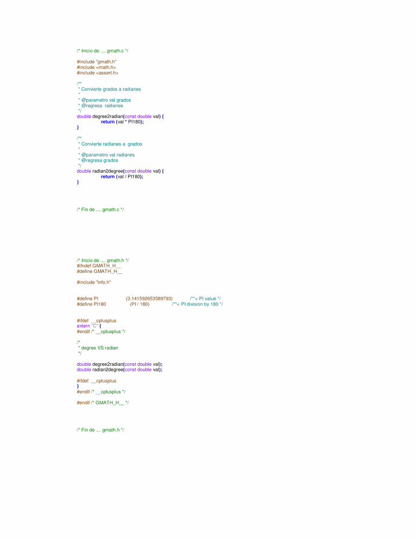
/* Inicio de .... gmath.c */ #include "gmath.h" #include <math.h> #include <assert.h> /** * Convierte grados a radianes * * @parametro val grados * @regresa radianes */ double degree2radian(const double val) return (val * PI180); /** * Convierte radianes a grados * * @parametro val radianes * @regresa grados */ double radian2degree(const double val) return (val / PI180); /* Fin de .... gmath.c */
/* Inicio de .... gmath.h */ #ifndef GMATH_H__ #define GMATH_H__ #include "info.h" #define PI (3.141592653589793) /**< PI value */ #define PI180 (PI / 180) /**< PI division by 180 */ #ifdef __cplusplus extern "C" #endif /* __cplusplus */ /* * degree VS radian */ double degree2radian(const double val); double radian2degree(const double val); #ifdef __cplusplus #endif /* __cplusplus */ #endif /* GMATH_H__ */ /* Fin de .... gmath.h */
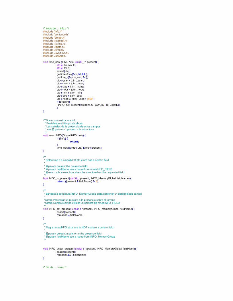
/* Inicio de .... info.c */ #include "info.h" #include "sentence.h" #include "gmath.h" #include <stdbool.h> #include <string.h> #include <math.h> #include <time.h> #include <sys/time.h> #include <assert.h> void time_now (TIME *utc, uint32_t * present) struct timeval tp; struct tm tt; assert(utc); gettimeofday(&tp, NULL ); gmtime_r(&tp.tv_sec, &tt); utc->year = tt.tm_year; utc->mon = tt.tm_mon; utc->day = tt.tm_mday; utc->hour = tt.tm_hour; utc->min = tt.tm_min; utc->sec = tt.tm_sec; utc->hsec = (tp.tv_usec / 1000); if (present) INFO_set_present(present, UTCDATE | UTCTIME); /**Borrar una estructura info. * Restablece el tiempo de ahora, * Las señales de la presencia de estos campos. * Info @ param un puntero a la estructura */ void zero_INFO(GlobalINFO *info) if (!info) return; time_now(&info->utc, &info->present); /** * Determine if a nmeaINFO structure has a certain field * * @param present the presence field * @param fieldName use a name from nmeaINFO_FIELD * @return a boolean, true when the structure has the requested field */ bool INFO_is_present(uint32_t present, INFO_MemoryGlobal fieldName) return ((present & fieldName) != 0); /** * Bandera a estructura INFO_MemoryGlobal para contener un determinado campo * *param Presentar un puntero a la presencia sobre el terreno *param NombreCampo utilizar un nombre de nmeaINFO_FIELD */ void INFO_set_present(uint32_t * present, INFO_MemoryGlobal fieldName) assert(present); *present |= fieldName; /** * Flag a nmeaINFO structure to NOT contain a certain field * * @param present a pointer to the presence field * @param fieldName use a name from INFO_MemoryGlobal */ void INFO_unset_present(uint32_t * present, INFO_MemoryGlobal fieldName) assert(present); *present &= ~fieldName; /* Fin de .... info.c */

/* Inicio de .... info.h */ #ifndef INFO_H__ #define INFO_H__ #include <stdint.h> #include <stdbool.h> #ifdef __cplusplus extern "C" #endif /* __cplusplus */ typedef struct _TIME int year; /**< Years since 1900 */ int mon; /**< Months since January - [0,11] */ int day; /**< Day of the month - [1,31] */ int hour; /**< Hours since midnight - [0,23] */ int min; /**< Minutes after the hour - [0,59] */ int sec; /**< Seconds after the minute - [0,59] */ int hsec; /**< Hundredth part of second - [0,99] */ TIME; typedef struct _GlobalINFO uint32_t present; int smask; TIME utc; int sig; /* PCHRP */ double pn_pchrp; double pe_pchrp; double alt_pchrp; double roll_pchrp; double pitch_pchrp; double yaw_pchrp; double heading_pchrp; /* PCHRH */ int SAT_USED; int SAT_IN_VIEW; double HDPO_PCHRH; int MODE_PCHRH; int COM_PCHRH; int ACCEL_PCHRH; int GYRO_PCHRH; int MAG_PCHRH; int GPS_PCHRH; int res1_PCHRH; int res2_PCHRH; int res3_PCHRH;
/* PCHRQ */ double a_pchrq; double b_pchrq; double c_pchrq; double d_pchrq; /* PCHRR */ double vn_pchrr; double ve_pchrr; double vu_pchrr; double roll_pchrr; double pitch_pchrr; double yaw_pchrr; /* PCHRS */ int count_pchrs; double sensor_x_pchrs; double sensor_y_pchrs; double sensor_z_pchrs;
/* gyros [0] */ double sensor_x_gyro; double sensor_y_gyro; double sensor_z_gyro; /* accell**[1] */ double sensor_x_acel; double sensor_y_acel; double sensor_z_acel;
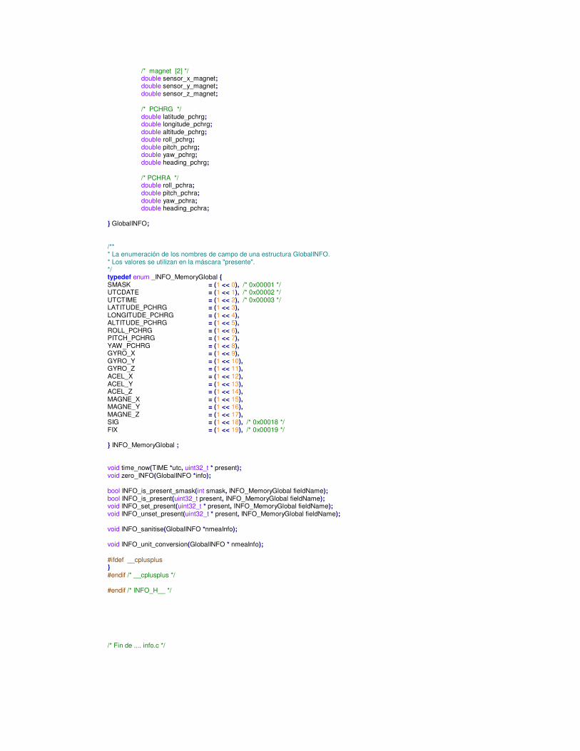
/* magnet [2] */ double sensor_x_magnet; double sensor_y_magnet; double sensor_z_magnet; /* PCHRG */ double latitude_pchrg; double longitude_pchrg; double altitude_pchrg; double roll_pchrg; double pitch_pchrg; double yaw_pchrg; double heading_pchrg; /* PCHRA */ double roll_pchra; double pitch_pchra; double yaw_pchra; double heading_pchra; GlobalINFO; /** * La enumeración de los nombres de campo de una estructura GlobalINFO. * Los valores se utilizan en la máscara "presente". */ typedef enum _INFO_MemoryGlobal SMASK = (1 << 0), /* 0x00001 */ UTCDATE = (1 << 1), /* 0x00002 */ UTCTIME = (1 << 2), /* 0x00003 */ LATITUDE_PCHRG = (1 << 3), LONGITUDE_PCHRG = (1 << 4), ALTITUDE_PCHRG = (1 << 5), ROLL_PCHRG = (1 << 6), PITCH_PCHRG = (1 << 7), YAW_PCHRG = (1 << 8), GYRO_X = (1 << 9), GYRO_Y = (1 << 10), GYRO_Z = (1 << 11), ACEL_X = (1 << 12), ACEL_Y = (1 << 13), ACEL_Z = (1 << 14), MAGNE_X = (1 << 15), MAGNE_Y = (1 << 16), MAGNE_Z = (1 << 17), SIG = (1 << 18), /* 0x00018 */ FIX = (1 << 19), /* 0x00019 */ INFO_MemoryGlobal ; void time_now(TIME *utc, uint32_t * present); void zero_INFO(GlobalINFO *info); bool INFO_is_present_smask(int smask, INFO_MemoryGlobal fieldName); bool INFO_is_present(uint32_t present, INFO_MemoryGlobal fieldName); void INFO_set_present(uint32_t * present, INFO_MemoryGlobal fieldName); void INFO_unset_present(uint32_t * present, INFO_MemoryGlobal fieldName); void INFO_sanitise(GlobalINFO *nmeaInfo); void INFO_unit_conversion(GlobalINFO * nmeaInfo); #ifdef __cplusplus #endif /* __cplusplus */ #endif /* INFO_H__ */
/* Fin de .... info.c */
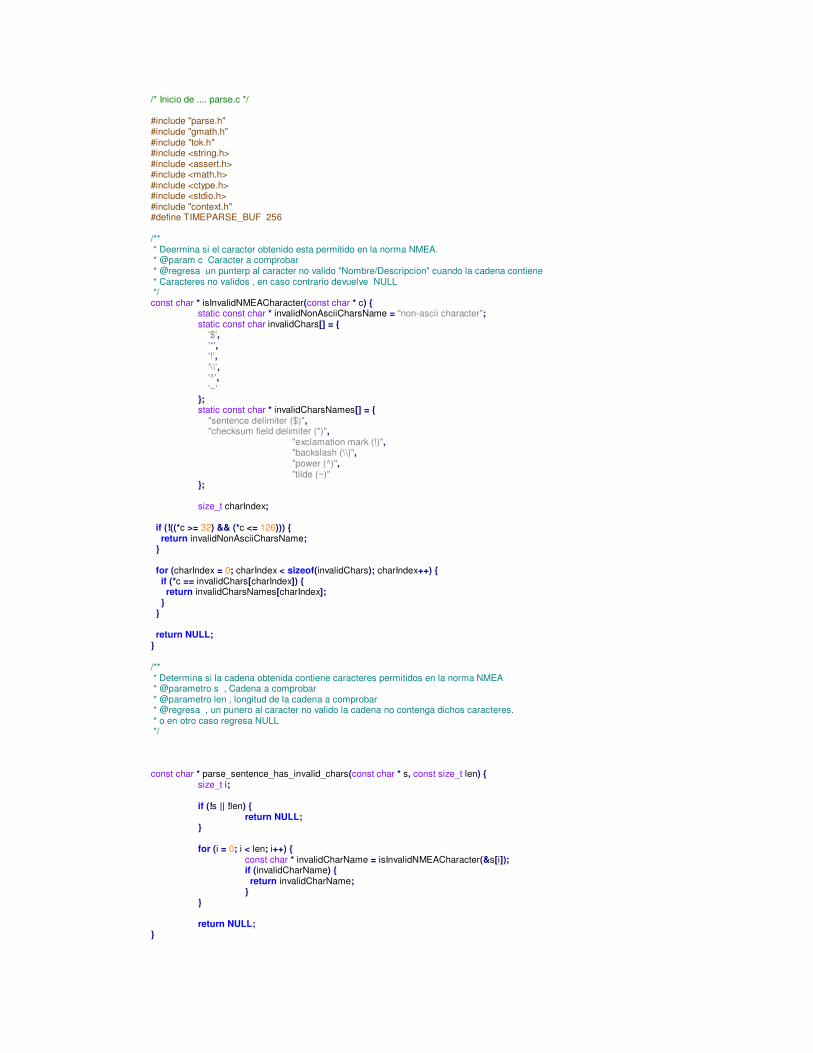
/* Inicio de .... parse.c */ #include "parse.h" #include "gmath.h" #include "tok.h" #include <string.h> #include <assert.h> #include <math.h> #include <ctype.h> #include <stdio.h> #include "context.h" #define TIMEPARSE_BUF 256 /** * Deermina si el caracter obtenido esta permitido en la norma NMEA. * @param c Caracter a comprobar * @regresa un punterp al caracter no valido "Nombre/Descripcion" cuando la cadena contiene * Caracteres no validos , en caso contrario devuelve NULL */ const char * isInvalidNMEACharacter(const char * c) static const char * invalidNonAsciiCharsName = "non-ascii character"; static const char invalidChars[] = '$', '*', '!', '\\', '^', '~' ; static const char * invalidCharsNames[] = "sentence delimiter ($)", "checksum field delimiter (*)", "exclamation mark (!)", "backslash (\\)", "power (^)", "tilde (~)" ; size_t charIndex; if (!((*c >= 32) && (*c <= 126))) return invalidNonAsciiCharsName; for (charIndex = 0; charIndex < sizeof(invalidChars); charIndex++) if (*c == invalidChars[charIndex]) return invalidCharsNames[charIndex]; return NULL; /** * Determina si la cadena obtenida contiene caracteres permitidos en la norma NMEA * @parametro s , Cadena a comprobar * @parametro len , longitud de la cadena a comprobar * @regresa , un punero al caracter no valido la cadena no contenga dichos caracteres. * o en otro caso regresa NULL */ const char * parse_sentence_has_invalid_chars(const char * s, const size_t len) size_t i; if (!s || !len) return NULL; for (i = 0; i < len; i++) const char * invalidCharName = isInvalidNMEACharacter(&s[i]); if (invalidCharName) return invalidCharName; return NULL;

/** * Determina que tipo de oracion o sentencia (ver en PACKTYPE) por el encabezado de una cadena. * la cabecera es la que se encuentra justo despues de "$" * @parametro s la cadena , debe ser una sentencia conocida , despues de "$" * @parametro len longitud de la cadena * @regresa el tipo de paquete o (GPNON cuando no puede ser determinado o no esta en lista) */ enum PACKTYPE parse_get_sentence_type(const char *s, const int len) static const char *pheads[] = "PCHRG","PCHRS","UM7A1" , ; static const enum PACKTYPE types[] = PCHRG , PCHRS , UM7A1 , ; unsigned int i; assert(s); if (len < 5) /* (len < 5)*/ return GPNON; for (i = 0; i < (sizeof(types) / sizeof(types[0])); i++) if (!memcmp(s, pheads[i], 5)) /* TOMA LAS PRIMERAS 5 LETRAS.*/ return types[i]; return GPNON; //================================= parse============================================// /// 1 2 3 4 5 6 7 8 9 // // $PCHRP,time, pn, pe, alt, roll, pitch, yaw, heading,/checksum// // $PCHRP,105.015,-501.234, -501.234,15.521,20.32,20.32, 20.32, 20.32, *47 // /** * Analiza una Cadena PCHRP * @parametro s , Cadena. * @parametro len longitud de la cadena. * @parametro has_checksum , es verdadero cuando la cadena contiene la suma de comprobacion. * @parametro pack , es el puntero a a la estructura de resultados. * @regresa 1 (true) - si es analizado correctamente o en caso contrario regresa 0 (False). */ int parse_PCHRP(const char *s, const int len, bool has_checksum, normaPCHRP *pack) int token_count; char time_buff[TIMEPARSE_BUF]; if (!has_checksum) return 0; assert(s); assert(pack); trace_buff(s, len); time_buff[0] = '\0'; pack->present = 0; pack->utc.year = -1; pack->utc.mon = -1; pack->utc.day = -1; pack->utc.hour = -1; pack->utc.min = -1; pack->utc.sec = -1; pack->utc.hsec = -1; /* 0 1 2 3 4 5 6 7 8 */ /* $PCHRP,time,pn,pe,alt,roll,pitch,yaw,heading, *checksum */ /* $PCHRP,105.015,-501.234,-501.234,15.521,20.32,20.32,20.32,20.32,*47*/
token_count = norma_scanf(s, len, "$PCHRP,%s,%f,%f,%f,%f,%f,%f,%f,%c*", &time_buff[0],&pack->pn_pchrp ,&pack->pe_pchrp, &pack->alt_pchrp, &pack->roll_pchrp,&pack->pitch_pchrp,&pack->yaw_pchrp,&pack->heading_pchrp);
if (token_count != 9) error("PCHRP parse error: need 9 tokens, got %d in %s", token_count, s); // printf("PCHRP parse error: need 9 tokens, got %d in %s\n",token_count,s); return 0; return 1;

/** * Analiza una Cadena PCHRH * * @parametro s , Cadena. * @parametro len longitud de la cadena. * @parametro has_checksum , es verdadero cuando la cadena contiene la suma de comprobacion. * @parametro pack , es el puntero a a la estructura de resultados. * @regresa 1 (true) - si es analizado correctamente o en caso contrario regresa 0 (False). */ int parse_PCHRH(const char *s, const int len, bool has_checksum, normaPCHRH *pack) int token_count; char time_buff[TIMEPARSE_BUF]; if (!has_checksum) return 0; assert(s); assert(pack); trace_buff(s, len); time_buff[0] = '\0'; pack->present = 0; pack->utc.year = -1; pack->utc.mon = -1; pack->utc.day = -1; pack->utc.hour = -1; pack->utc.min = -1; pack->utc.sec = -1; pack->utc.hsec = -1; /* parse */ /* 0 1 2 3 4 5 6 7 8 9 10 11 12 */ /* $PCHRH,time,sats_used,sats_in_view,HDOP,mode,COM,accel ,gyro,mag,GPS,res,res,res,*/ /* $PCHRH,105.015,05,11,1.5,0,0,0,0,0,0,0,0,0,\r\n", */ token_count = norma_scanf(s, len, "$PCHRH,%s,%i,%i,%f,%i,%i,%i,%i,%i,%i,%i,%i,%c*", &time_buff[0], &pack->SAT_USED,&pack->SAT_IN_VIEW , &pack->HDPO_PCHRH, &pack->MODE_PCHRH,&pack->COM_PCHRH,&pack->ACCEL_PCHRH,&pack->GYRO_PCHRH, &pack->MAG_PCHRH,&pack->GPS_PCHRH,&pack->res1_PCHRH,&pack->res2_PCHRH, &pack->res3_PCHRH); if (token_count != 13) error("PCHRH parse error: need 13 tokens, got %d in %s", token_count, s); // printf("PCHRP parse error: need 9 tokens, got %d in %s\n",token_count,s); return 0; return 1;
/** * Analiza una Cadena PCHRA * @parametro s , Cadena. * @parametro len longitud de la cadena. * @parametro has_checksum , es verdadero cuando la cadena contiene la suma de comprobacion. * @parametro pack , es el puntero a a la estructura de resultados. * @regresa 1 (true) - si es analizado correctamente o en caso contrario regresa 0 (False). */ int parse_PCHRA(const char *s, const int len, bool has_checksum, normaPCHRA *pack) int token_count; char time_buff[TIMEPARSE_BUF]; if (!has_checksum) return 0; assert(s); assert(pack); trace_buff(s, len); time_buff[0] = '\0'; pack->present = 0; pack->utc.year = -1; pack->utc.mon = -1; pack->utc.day = -1;

pack->utc.hour = -1; pack->utc.min = -1; pack->utc.sec = -1; pack->utc.hsec = -1; /* parse */ // 0 1 2 3 4 5 //$PCHRA, time, roll, pitch,yaw, heading,chcksum // $PCHRA,105.015,20.32,20.32,20.32,20.32,*66" token_count = norma_scanf(s, len, "$PCHRA,%s,%f,%f,%f,%f,%c*", &time_buff[0], &pack->roll_pchra, &pack->pitch_pchra, &pack->yaw_pchra, &pack->heading_pchra); if (token_count != 6) error("PCHRA parse error: need 6 tokens, got %d in %s", token_count, s); // printf("PCHRA parse error: need x tokens, got %d in %s\n",token_count,s); return 0; return 1; /** * Analiza una Cadena PCHRS * * @parametro s , Cadena. * @parametro len longitud de la cadena. * @parametro has_checksum , es verdadero cuando la cadena contiene la suma de comprobacion. * @parametro pack , es el puntero a a la estructura de resultados. * @regresa 1 (true) - si es analizado correctamente o en caso contrario regresa 0 (False). */ int parse_PCHRS(const char *s, const int len, bool has_checksum, normaPCHRS *pack) int token_count; char time_buff[TIMEPARSE_BUF]; if (!has_checksum) return 0; assert(s); assert(pack); trace_buff(s, len); time_buff[0] = '\0'; pack->present = 0; pack->utc.year = -1; pack->utc.mon = -1; pack->utc.day = -1; pack->utc.hour = -1; pack->utc.min = -1; pack->utc.sec = -1; pack->utc.hsec = -1; // 0 1 2 3 4 5 // $PCHRS, count time, sensor_x sensor_y sensor_z chcksum // $PCHRS, 1, 105.015, -0.9987, -0.9987, -0.9987, *79\r\n",
token_count = norma_scanf(s, len, "$PCHRS,%i,%s,%f,%f,%f,%c*", &pack->count_pchrs,&time_buff[0],&pack->sensor_x_pchrs,
&pack->sensor_y_pchrs,&pack->sensor_z_pchrs); if (token_count != 6) error("PCHRS parse error: need 6 tokens, got %d in %s", token_count, s); //printf("PCHRS parse error: need 6 tokens, got %d in %s\n",token_count,s); return 0; return 1; /** * Analiza una Cadena PCHRR * * @parametro s , Cadena. * @parametro len longitud de la cadena. * @parametro has_checksum , es verdadero cuando la cadena contiene la suma de comprobacion. * @parametro pack , es el puntero a a la estructura de resultados. * @regresa 1 (true) - si es analizado correctamente o en caso contrario regresa 0 (False). */ int parse_PCHRR(const char *s, const int len, bool has_checksum, normaPCHRR *pack) int token_count;

char time_buff[TIMEPARSE_BUF]; if (!has_checksum) return 0; assert(s); assert(pack); trace_buff(s, len); time_buff[0] = '\0'; pack->present = 0; pack->utc.year = -1; pack->utc.mon = -1; pack->utc.day = -1; pack->utc.hour = -1; pack->utc.min = -1; pack->utc.sec = -1; pack->utc.hsec = -1; // 0 1 2 3 4 5 6 7// // $PCHRR, time, vn,ve,vup,roll_rate,pitch_rate,yaw_rate checksum // "$PCHRR,105.015,15.23,15.23,15.23,-450.26,-450.26, -450.26,*68\r\n",, token_count = norma_scanf(s, len, "$PCHRR,%s,%f,%f,%f,%f,%f,%f,%c*",
&time_buff[0],&pack->vn_pchrr,&pack->ve_pchrr,&pack->vu_pchrr, &pack->roll_pchrr,&pack->pitch_pchrr,&pack->yaw_pchrr); if (token_count != 8) error("PCHRR parse error: need 8 tokens, got %d in %s", token_count, s); //printf("PCHRP parse error: need 8 tokens, got %d in %s\n",token_count,s); return 0; return 1; /** * Analiza una Cadena PCHRG * @parametro s , Cadena. * @parametro len longitud de la cadena. * @parametro has_checksum , es verdadero cuando la cadena contiene la suma de comprobacion. * @parametro pack , es el puntero a a la estructura de resultados. * @regresa 1 (true) - si es analizado correctamente o en caso contrario regresa 0 (False). */ int parse_PCHRG(const char *s, const int len, bool has_checksum, normaPCHRG *pack) int token_count; char time_buff[TIMEPARSE_BUF]; if (!has_checksum) return 0; assert(s); assert(pack); trace_buff(s, len); time_buff[0] = '\0'; pack->present = 0; pack->utc.year = -1; pack->utc.mon = -1; pack->utc.day = -1; pack->utc.hour = -1; pack->utc.min = -1; pack->utc.sec = -1; pack->utc.hsec = -1;
// 0 1 2 3 4 5 6 7 8 // //$PCHRG,time,LATITUDE,LONGITUDE,ALTITUDE,roll_PCHRG,pitch_PCHRG,yaw_PCHRG,HEADING,checksum //"$PCHRG,105.015,40.047706,-111.742072,15.230,20.32,20.32,20.32,20.32,*49\r\n",",,// token_count = norma_scanf(s, len, "$PCHRG,%s,%f,%f,%f,%f,%f,%f*", &time_buff[0], &pack->latitude_pchrg,&pack->longitude_pchrg, &pack->altitude_pchrg, &pack->roll_pchrg,&pack->pitch_pchrg, &pack->yaw_pchrg); if (token_count != 7) error("PCHRG parse error: need 7 tokens, got %d in %s", token_count, s); //printf("PCHRG parse error: need 7 tokens, got %d in %s\n",token_count,s); return 0; return 1; /** * Analiza una Cadena PCHRQ * * @parametro s , Cadena. * @parametro len longitud de la cadena. * @parametro has_checksum , es verdadero cuando la cadena contiene la suma de comprobacion.

* @parametro pack , es el puntero a a la estructura de resultados. * @regresa 1 (true) - si es analizado correctamente o en caso contrario regresa 0 (False). */ int parse_PCHRQ(const char *s, const int len, bool has_checksum, normaPCHRQ *pack) int token_count; char time_buff[TIMEPARSE_BUF]; if (!has_checksum) return 0; assert(s); assert(pack); trace_buff(s, len); time_buff[0] = '\0'; pack->present = 0; pack->utc.year = -1; pack->utc.mon = -1; pack->utc.day = -1; pack->utc.hour = -1; pack->utc.min = -1; pack->utc.sec = -1; pack->utc.hsec = -1; // 0 1 2 3 4 5 // $PCHRQ,time,A, B, C,D,checksum // "$PCHRQ, 105.015,0.76592,0.76592,0.76592,0.76592 ,*60\r\n",,,,
token_count = norma_scanf(s, len, "$PCHRQ,%s,%f,%f,%f,%f,%d*", &time_buff[0],&pack->a_pchrq,&pack->b_pchrq,
&pack->c_pchrq,&pack->d_pchrq); if (token_count != 6) error("PCHRQ parse error: need 6 tokens, got %d in %s", token_count, s); //printf("PCHRq parse error: need 6 tokens, got %d in %s\n",token_count,s); return 0; return 1; /* Fin de .... parse.c */ /* Inicio de .... parse.h */ #ifndef PARSE_H__ #define PARSE_H__ #include "sentence.h" #include <stdbool.h> #include <stddef.h> #ifdef __cplusplus extern "C" #endif /* __cplusplus */ const char * isInvalidNMEACharacter(const char * c); const char * parse_sentence_has_invalid_chars(const char * s, const size_t len); enum PACKTYPE parse_get_sentence_type(const char *s, const int len); int parse_PCHRP(const char *s, const int len, bool has_checksum, normaPCHRP *pack); int parse_PCHRH(const char *s, const int len, bool has_checksum, normaPCHRH *pack); int parse_PCHRA(const char *s, const int len, bool has_checksum, normaPCHRA *pack); int parse_PCHRS(const char *s, const int len, bool has_checksum, normaPCHRS *pack); int parse_PCHRR(const char *s, const int len, bool has_checksum, normaPCHRR *pack); int parse_PCHRG(const char *s, const int len, bool has_checksum, normaPCHRG *pack); int parse_PCHRQ(const char *s, const int len, bool has_checksum, normaPCHRQ *pack); #ifdef __cplusplus #endif /* __cplusplus */ #endif /* PARSE_H__ */ /* Fin de .... parse.h */

/* Inicio de .... parser.c */ #include "parser.h" #include "parse.h" #include "sentence.h" #include "conversions.h" #include "tok.h" #include <stdlib.h> #include <stdbool.h> #include <string.h> #include <assert.h> #include <ctype.h> #define first_eol_char ('\r') #define second_eol_char ('\n') static void reset_sentence_parser(PARSER * parser, sentence_parser_state new_state) assert(parser); memset(&parser->sentence_parser, 0, sizeof(parser->sentence_parser)); parser->buffer.buffer[0] = '\0'; parser->buffer.length = 0; parser->sentence_parser.has_checksum = false; parser->sentence_parser.state = new_state; int parser_init(PARSER *parser) assert(parser); memset(&parser->sentence, 0, sizeof(parser->sentence)); reset_sentence_parser(parser, SKIP_UNTIL_START); return 1; static inline bool isHexChar(char c) switch (tolower(c)) case '0': case '1': case '2': case '3': case '4': case '5': case '6': case '7': case '8': case '9': case 'a': case 'b': case 'c': case 'd': case 'e':
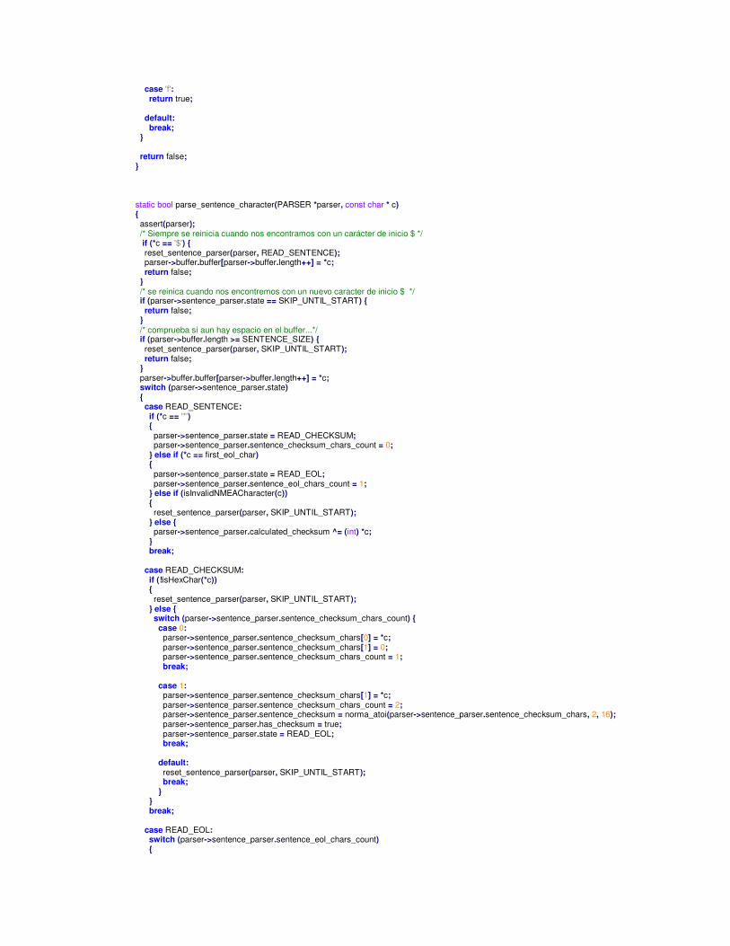
case 'f': return true; default: break; return false; static bool parse_sentence_character(PARSER *parser, const char * c) assert(parser); /* Siempre se reinicia cuando nos encontramos con un carácter de inicio $ */ if (*c == '$') reset_sentence_parser(parser, READ_SENTENCE); parser->buffer.buffer[parser->buffer.length++] = *c; return false; /* se reinica cuando nos encontremos con un nuevo caracter de inicio $ */ if (parser->sentence_parser.state == SKIP_UNTIL_START) return false; /* comprueba si aun hay espacio en el buffer...*/ if (parser->buffer.length >= SENTENCE_SIZE) reset_sentence_parser(parser, SKIP_UNTIL_START); return false; parser->buffer.buffer[parser->buffer.length++] = *c; switch (parser->sentence_parser.state) case READ_SENTENCE: if (*c == '*') parser->sentence_parser.state = READ_CHECKSUM; parser->sentence_parser.sentence_checksum_chars_count = 0; else if (*c == first_eol_char) parser->sentence_parser.state = READ_EOL; parser->sentence_parser.sentence_eol_chars_count = 1; else if (isInvalidNMEACharacter(c)) reset_sentence_parser(parser, SKIP_UNTIL_START); else parser->sentence_parser.calculated_checksum ^= (int) *c; break; case READ_CHECKSUM: if (!isHexChar(*c)) reset_sentence_parser(parser, SKIP_UNTIL_START); else switch (parser->sentence_parser.sentence_checksum_chars_count) case 0: parser->sentence_parser.sentence_checksum_chars[0] = *c; parser->sentence_parser.sentence_checksum_chars[1] = 0; parser->sentence_parser.sentence_checksum_chars_count = 1; break; case 1: parser->sentence_parser.sentence_checksum_chars[1] = *c; parser->sentence_parser.sentence_checksum_chars_count = 2; parser->sentence_parser.sentence_checksum = norma_atoi(parser->sentence_parser.sentence_checksum_chars, 2, 16); parser->sentence_parser.has_checksum = true; parser->sentence_parser.state = READ_EOL; break; default: reset_sentence_parser(parser, SKIP_UNTIL_START); break; break; case READ_EOL: switch (parser->sentence_parser.sentence_eol_chars_count)

case 0: if (*c != first_eol_char) reset_sentence_parser(parser, SKIP_UNTIL_START); else parser->sentence_parser.sentence_eol_chars_count = 1; break; case 1: if (*c != second_eol_char) reset_sentence_parser(parser, SKIP_UNTIL_START); else parser->sentence_parser.state = SKIP_UNTIL_START; return (!parser->sentence_parser.sentence_checksum_chars_count || (parser->sentence_parser.sentence_checksum_chars_count && (parser->sentence_parser.sentence_checksum == parser->sentence_parser.calculated_checksum))); break; default: reset_sentence_parser(parser, SKIP_UNTIL_START); break; break; case SKIP_UNTIL_START: default: break; return false; /** * Analizar una cadena y almacenar los resultados en la estructura GlobalINFO @parametro parse pará- un puntero al analizador @parametro -s la cadena @parametro -len la longitud de la cadena @parametro -info un puntero a la estructura globalINFO devolver el número de paquetes que se analiza * */ int parse(PARSER * parser, const char * s, int len, GlobalINFO * info) int sentences_count = 0; int charIndex = 0; assert(parser); /*comprobar presencia*/ assert(s); /*comprobar presencia*/ assert(info); /*comprobar presencia*/ for (charIndex = 0; charIndex < len; charIndex++) bool sentence_read_successfully = parse_sentence_character(parser, &s[charIndex]); if (sentence_read_successfully) enum PACKTYPE sentence_type = parse_get_sentence_type(&parser->buffer.buffer[1], parser->buffer.length - 1); switch (sentence_type) case PCHRS: if (parse_PCHRS(parser->buffer.buffer, parser->buffer.length, parser->sentence_parser.has_checksum, &parser->sentence.pchrs)) sentences_count++; PCHRS2info(&parser->sentence.pchrs, info); break; case PCHRG: if (parse_PCHRG(parser->buffer.buffer, parser->buffer.length, parser->sentence_parser.has_checksum, &parser->sentence.pchrg)) sentences_count++; PCHRG2info(&parser->sentence.pchrg, info); break; /*************** debug *******************************************/ /* case PCHRP: // printf("pase por el Switch PCHRP\n"); if (parse_PCHRP(parser->buffer.buffer, parser->buffer.length, parser->sentence_parser.has_checksum, &parser->sentence.pchrp)) sentences_count++; PCHRP2info(&parser->sentence.pchrp, info);
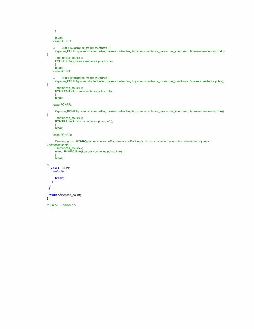
break; case PCHRH: // printf("pase por el Switch PCHRH\n"); if (parse_PCHRH(parser->buffer.buffer, parser->buffer.length, parser->sentence_parser.has_checksum, &parser->sentence.pchrh)) sentences_count++; PCHRH2info(&parser->sentence.pchrh, info); break; case PCHRA: // printf("pase por el Switch PCHRA\n"); if (parse_PCHRA(parser->buffer.buffer, parser->buffer.length, parser->sentence_parser.has_checksum, &parser->sentence.pchra)) sentences_count++; PCHRA2info(&parser->sentence.pchra, info); break; case PCHRR: if (parse_PCHRR(parser->buffer.buffer, parser->buffer.length, parser->sentence_parser.has_checksum, &parser->sentence.pchrr)) sentences_count++; PCHRR2info(&parser->sentence.pchrr, info); break; case PCHRQ: if (nmea_parse_PCHRQ(parser->buffer.buffer, parser->buffer.length, parser->sentence_parser.has_checksum, &parser->sentence.pchrq)) sentences_count++; nmea_PCHRQ2info(&parser->sentence.pchrq, info); break; */ case GPNON: default: break; return sentences_count; /* Fin de .... parser.c */

/* Inicio de .... parser.h */ #ifndef PARSER_H__ #define PARSER_H__ #include "info.h" #include "sentence.h" #ifdef __cplusplus extern "C" #endif /* __cplusplus */ #ifdef NMEA_MAX_SENTENCE_LENGTH /* override the default maximum sentence length */ #define SENTENCE_SIZE (NMEA_MAX_SENTENCE_LENGTH) #else /* we need to be able to parse much longer sentences than specified in the (original) specification */ #define SENTENCE_SIZE (4096 * 1) #endif typedef enum _sentence_parser_state SKIP_UNTIL_START, READ_SENTENCE, READ_CHECKSUM, READ_EOL sentence_parser_state; typedef struct _sentencePARSER int sentence_checksum; int calculated_checksum; char sentence_checksum_chars[2]; char sentence_checksum_chars_count; char sentence_eol_chars_count; bool has_checksum; sentence_parser_state state; sentencePARSER; typedef struct _PARSER struct unsigned int length; char buffer[SENTENCE_SIZE]; buffer; union normaPCHRH pchrh; normaPCHRP pchrp; normaPCHRA pchra; normaPCHRS pchrs; normaPCHRR pchrr; normaPCHRG pchrg; normaPCHRQ pchrq; bbbUM7A1 um7a1; sentence; sentencePARSER sentence_parser; PARSER; int parser_init(PARSER *parser); int parse(PARSER * parser, const char * s, int len, GlobalINFO * info); #ifdef __cplusplus #endif /* __cplusplus */ #endif /* PARSER_H__ */ /* Fin de .... parser.h */

/* Inicio de .... sentence.c */ #include "sentence.h" #include <string.h> void zero_PCHRP(normaPCHRP *pack) memset(pack, 0, sizeof(normaPCHRP)); void zero_PCHRH(normaPCHRH *pack) memset(pack, 0, sizeof(normaPCHRH)); void zero_PCHRG(normaPCHRG *pack) memset(pack, 0, sizeof(normaPCHRG)); void zero_UM7A1(bbbUM7A1 *pack) memset(pack, 0, sizeof(bbbUM7A1)); /* Fin de .... sentence.c */
/* Inicio de .... sentence.h */ #ifndef SENTENCE_H__ #define SENTENCE_H__ #include "info.h" #include <stdint.h> #ifdef __cplusplus extern "C" #endif /* __cplusplus */ enum PACKTYPE GPNON = 0,
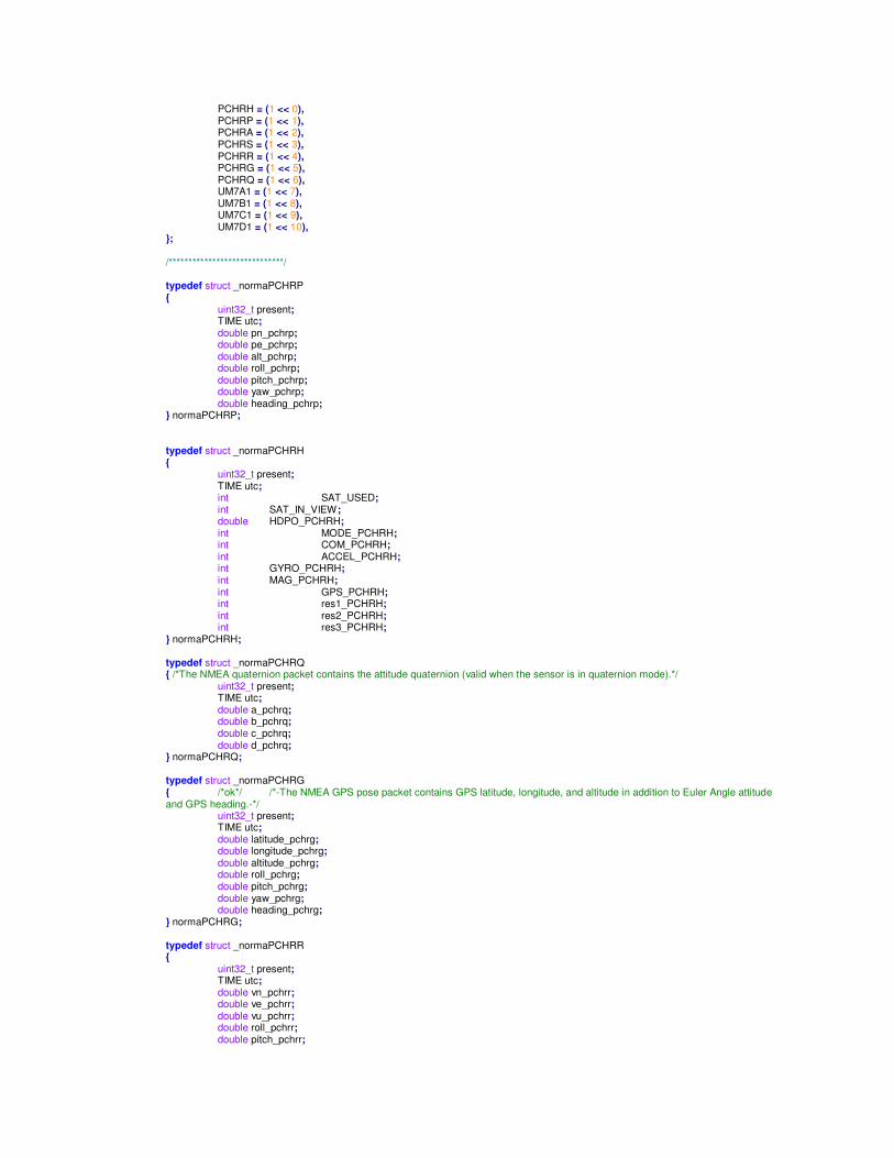
PCHRH = (1 << 0), PCHRP = (1 << 1), PCHRA = (1 << 2), PCHRS = (1 << 3), PCHRR = (1 << 4), PCHRG = (1 << 5), PCHRQ = (1 << 6), UM7A1 = (1 << 7), UM7B1 = (1 << 8), UM7C1 = (1 << 9), UM7D1 = (1 << 10), ; /*****************************/ typedef struct _normaPCHRP uint32_t present; TIME utc; double pn_pchrp; double pe_pchrp; double alt_pchrp; double roll_pchrp; double pitch_pchrp; double yaw_pchrp; double heading_pchrp; normaPCHRP; typedef struct _normaPCHRH uint32_t present; TIME utc; int SAT_USED; int SAT_IN_VIEW; double HDPO_PCHRH; int MODE_PCHRH; int COM_PCHRH; int ACCEL_PCHRH; int GYRO_PCHRH; int MAG_PCHRH; int GPS_PCHRH; int res1_PCHRH; int res2_PCHRH; int res3_PCHRH; normaPCHRH; typedef struct _normaPCHRQ /*The NMEA quaternion packet contains the attitude quaternion (valid when the sensor is in quaternion mode).*/ uint32_t present; TIME utc; double a_pchrq; double b_pchrq; double c_pchrq; double d_pchrq; normaPCHRQ; typedef struct _normaPCHRG /*ok*/ /*-The NMEA GPS pose packet contains GPS latitude, longitude, and altitude in addition to Euler Angle attitude and GPS heading.-*/ uint32_t present; TIME utc; double latitude_pchrg; double longitude_pchrg; double altitude_pchrg; double roll_pchrg; double pitch_pchrg; double yaw_pchrg; double heading_pchrg; normaPCHRG; typedef struct _normaPCHRR uint32_t present; TIME utc; double vn_pchrr; double ve_pchrr; double vu_pchrr; double roll_pchrr; double pitch_pchrr;
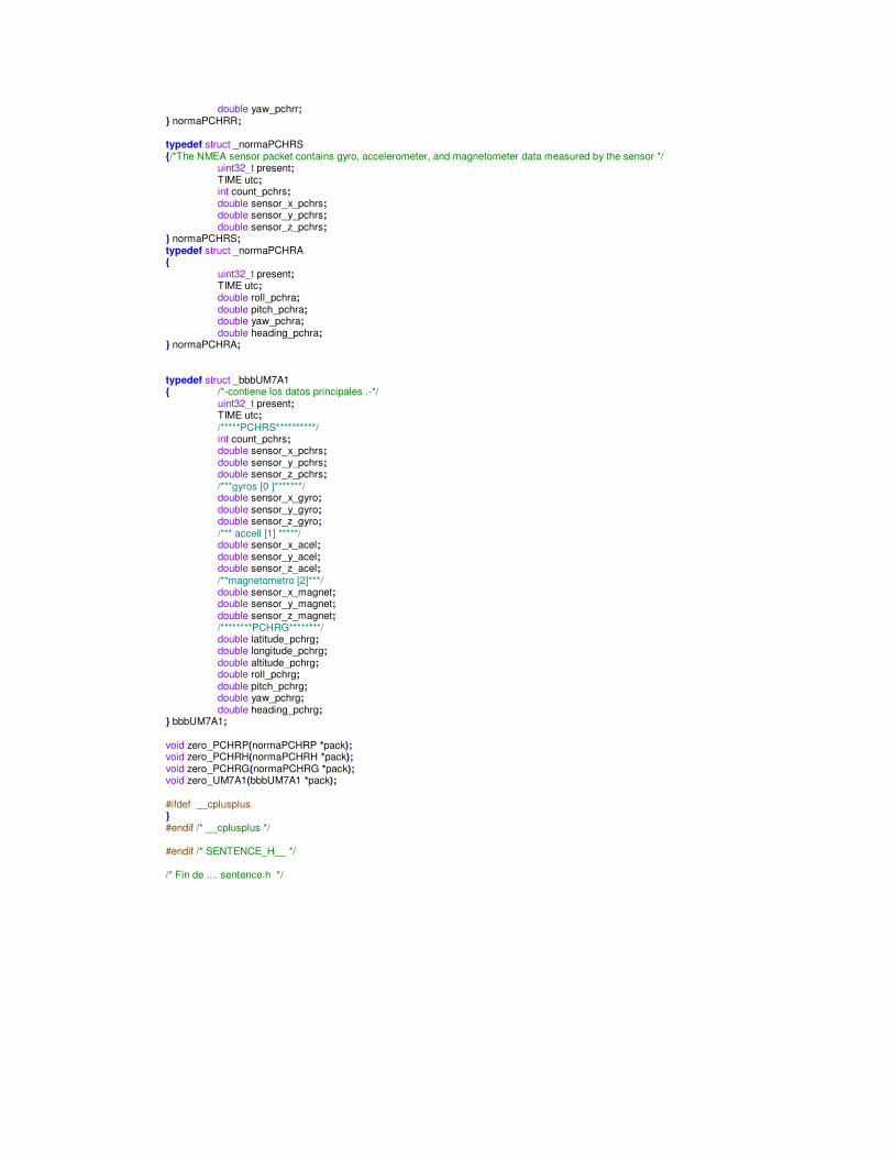
double yaw_pchrr; normaPCHRR; typedef struct _normaPCHRS /*The NMEA sensor packet contains gyro, accelerometer, and magnetometer data measured by the sensor */ uint32_t present; TIME utc; int count_pchrs; double sensor_x_pchrs; double sensor_y_pchrs; double sensor_z_pchrs; normaPCHRS; typedef struct _normaPCHRA uint32_t present; TIME utc; double roll_pchra; double pitch_pchra; double yaw_pchra; double heading_pchra; normaPCHRA; typedef struct _bbbUM7A1 /*-contiene los datos principales .-*/ uint32_t present; TIME utc; /*****PCHRS**********/ int count_pchrs; double sensor_x_pchrs; double sensor_y_pchrs; double sensor_z_pchrs; /***gyros [0 ]*******/ double sensor_x_gyro; double sensor_y_gyro; double sensor_z_gyro; /*** accell [1] *****/ double sensor_x_acel; double sensor_y_acel; double sensor_z_acel; /**magnetometro [2]***/ double sensor_x_magnet; double sensor_y_magnet; double sensor_z_magnet; /********PCHRG********/ double latitude_pchrg; double longitude_pchrg; double altitude_pchrg; double roll_pchrg; double pitch_pchrg; double yaw_pchrg; double heading_pchrg; bbbUM7A1; void zero_PCHRP(normaPCHRP *pack); void zero_PCHRH(normaPCHRH *pack); void zero_PCHRG(normaPCHRG *pack); void zero_UM7A1(bbbUM7A1 *pack); #ifdef __cplusplus #endif /* __cplusplus */ #endif /* SENTENCE_H__ */ /* Fin de .... sentence.h */
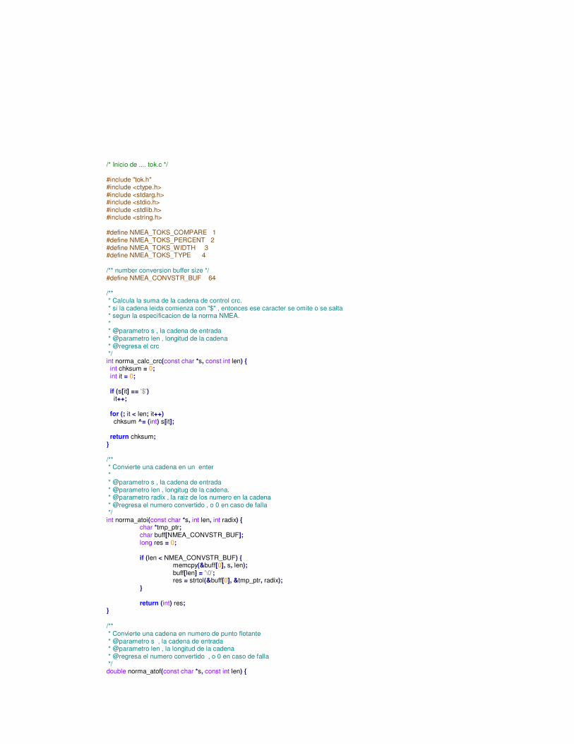
/* Inicio de .... tok.c */ #include "tok.h" #include <ctype.h> #include <stdarg.h> #include <stdio.h> #include <stdlib.h> #include <string.h> #define NMEA_TOKS_COMPARE 1 #define NMEA_TOKS_PERCENT 2 #define NMEA_TOKS_WIDTH 3 #define NMEA_TOKS_TYPE 4 /** number conversion buffer size */ #define NMEA_CONVSTR_BUF 64 /** * Calcula la suma de la cadena de control crc. * si la cadena leida comienza con "$" , entonces ese caracter se omite o se salta * segun la especificacion de la norma NMEA. * * @parametro s , la cadena de entrada * @parametro len , longitud de la cadena * @regresa el crc */ int norma_calc_crc(const char *s, const int len) int chksum = 0; int it = 0; if (s[it] == '$') it++; for (; it < len; it++) chksum ^= (int) s[it]; return chksum; /** * Convierte una cadena en un enter * * @parametro s , la cadena de entrada * @parametro len , longitug de la cadena. * @parametro radix , la raiz de los numero en la cadena * @regresa el numero convertido , o 0 en caso de falla */ int norma_atoi(const char *s, int len, int radix) char *tmp_ptr; char buff[NMEA_CONVSTR_BUF]; long res = 0; if (len < NMEA_CONVSTR_BUF) memcpy(&buff[0], s, len); buff[len] = '\0'; res = strtol(&buff[0], &tmp_ptr, radix); return (int) res; /** * Convierte una cadena en numero de punto flotante * @parametro s , la cadena de entrada * @parametro len , la longitud de la cadena * @regresa el numero convertido , o 0 en caso de falla */ double norma_atof(const char *s, const int len)

char *tmp_ptr; char buff[NMEA_CONVSTR_BUF]; double res = 0; if (len < NMEA_CONVSTR_BUF) memcpy(&buff[0], s, len); buff[len] = '\0'; res = strtod(&buff[0], &tmp_ptr); return res; /** * Formating string (like standart printf) with CRC tail (*CRC) * * @param s the string buffer to printf into * @param len the size of the string buffer * @param format the string format to use * @return the number of printed characters */ int norma_printf(char *s, int len, const char *format, ...) int retval; int add = 0; va_list arg_ptr; if (len <= 0) return 0; va_start(arg_ptr, format); retval = vsnprintf(s, len, format, arg_ptr); if (retval > 0) add = snprintf(s + retval, len - retval, "*%02x\r\n", norma_calc_crc(s + 1, retval - 1)); retval += add; if (retval < 0 || retval > len) memset(s, ' ', len); retval = len; va_end(arg_ptr); return retval; /** * Analyse a string (specific for NMEA sentences) * * @param s the string * @param len the length of the string * @param format the string format to use * @return the number of scanned characters */ int norma_scanf(const char *s, int len, const char *format, ...) const char *beg_tok; const char *end_buf = s + len; va_list arg_ptr; int tok_type = NMEA_TOKS_COMPARE; int width = 0; const char *beg_fmt = 0; int snum = 0, unum = 0; int tok_count = 0; void *parg_target; va_start(arg_ptr, format); for (; *format && s < end_buf; format++) switch (tok_type) case NMEA_TOKS_COMPARE: if ('%' == *format) tok_type = NMEA_TOKS_PERCENT; else if (*s++ != *format) goto fail; break; case NMEA_TOKS_PERCENT:

width = 0; beg_fmt = format; tok_type = NMEA_TOKS_WIDTH; /* no break */ case NMEA_TOKS_WIDTH: if (isdigit(*format)) break; tok_type = NMEA_TOKS_TYPE; if (format > beg_fmt) width = norma_atoi(beg_fmt, (int) (format - beg_fmt), 10); /* no break */ case NMEA_TOKS_TYPE: beg_tok = s; if (!width && ('c' == *format || 'C' == *format) && *s != format[1]) width = 1; if (width) if (s + width <= end_buf) s += width; else goto fail; else if (!format[1] || (0 == (s = (char *) memchr(s, format[1], end_buf - s)))) s = end_buf; if (s > end_buf) goto fail; tok_type = NMEA_TOKS_COMPARE; tok_count++; parg_target = 0; width = (int) (s - beg_tok); switch (*format) case 'c': case 'C': parg_target = (void *) va_arg(arg_ptr, char *); if (width && 0 != (parg_target)) *((char *) parg_target) = *beg_tok; break; case 's': case 'S': parg_target = (void *) va_arg(arg_ptr, char *); if (width && 0 != (parg_target)) memcpy(parg_target, beg_tok, width); ((char *) parg_target)[width] = '\0'; break; case 'f': case 'g': case 'G': case 'e': case 'E': parg_target = (void *) va_arg(arg_ptr, double *); if (width && 0 != (parg_target)) *((double *) parg_target) = norma_atof(beg_tok, width); break; default: break; ; if (parg_target) break; if (0 == (parg_target = (void *) va_arg(arg_ptr, int *))) break; if (!width) break; switch (*format) case 'd': case 'i': snum = norma_atoi(beg_tok, width, 10); memcpy(parg_target, &snum, sizeof(int));

break; case 'u': unum = norma_atoi(beg_tok, width, 10); memcpy(parg_target, &unum, sizeof(unsigned int)); break; case 'x': case 'X': unum = norma_atoi(beg_tok, width, 16); memcpy(parg_target, &unum, sizeof(unsigned int)); break; case 'o': unum = norma_atoi(beg_tok, width, 8); memcpy(parg_target, &unum, sizeof(unsigned int)); break; default: goto fail; ; break; default: break; ; fail: va_end(arg_ptr); return tok_count; /* Fin de .... tok.c */
/* Inicio de .... tok.h */ #ifndef TOK_H__ #define TOK_H__ #ifdef __cplusplus extern "C" #endif /* __cplusplus */ int norma_calc_crc(const char *s, const int len); int norma_atoi(const char *s, const int len, const int radix); double norma_atof(const char *s, const int len); int norma_printf(char *s, int len, const char *format, ...) __attribute__ ((format(printf, 3, 4))); int norma_scanf(const char *s, int len, const char *format, ...); #ifdef __cplusplus #endif /* __cplusplus */ #endif /* TOK_H__ */ /* Fin de .... tok.h */

REF: BBONEBLK_SRM BeagleBone Black System Reference Manual
Rev A5.2
Page 1 of 108
BeagleBone Black
System
Reference Manual
Revision A5.2
April 11, 2013
Author: Gerald Coley
Contributing Editor: Robert P J Day

REF: BBONEBLK_SRM BeagleBone Black System Reference Manual
Rev A5.2
Page 2 of 108
THIS DOCUMENT
This work is licensed under the Creative Commons Attribution-Share Alike 3.0 Unported
License. To view a copy of this license, visit http://creativecommons.org/licenses/by-
sa/3.0/ or send a letter to Creative Commons, 171 Second Street, Suite 300, San
Francisco, California, 94105, USA.
All derivative works are to be attributed to Gerald Coley of BeagleBoard.org.
For more information, see http://creativecommons.org/license/results-
one?license_code=by-sa
Send all comments and errors concerning this document to the author at
For other questions you may contact Gerald at:
Gerald Coley
Texas Instruments
12500 TI Blvd. Dallas, Tx 75243
All information in this document is subject to change without notice.
For an up to date version of this document refer to:
http://circuitco.com/support/index.php?title=BeagleBoneBlack#LATEST_PRODUC
TION_FILES_.28A5A.29

REF: BBONEBLK_SRM BeagleBone Black System Reference Manual
Rev A5.2
Page 3 of 108
BEAGLEBONE DESIGN
These design materials referred to in this document are *NOT SUPPORTED* and DO NOT constitute a reference design. Only “community” support is allowed via resources at BeagleBoard.org/discuss. THERE IS NO WARRANTY FOR THE DESIGN MATERIALS, TO THE EXTENT PERMITTED BY APPLICABLE LAW. EXCEPT WHEN OTHERWISE STATED IN WRITING THE COPYRIGHT HOLDERS AND/OR OTHER PARTIES PROVIDE THE DESIGN MATERIALS “AS IS” WITHOUT WARRANTY OF ANY KIND, EITHER EXPRESSED OR IMPLIED, INCLUDING, BUT NOT LIMITED TO, THE IMPLIED WARRANTIES OF MERCHANTABILITY AND FITNESS FOR A PARTICULAR PURPOSE. THE ENTIRE RISK AS TO THE QUALITY AND PERFORMANCE OF THE DESIGN MATERIALS IS WITH YOU. SHOULD THE DESIGN MATERIALS PROVE DEFECTIVE, YOU ASSUME THE COST OF ALL NECESSARY SERVICING, REPAIR OR CORRECTION. This board was designed as an evaluation and development tool. It was not designed with any other application in mind. As such, these design materials may or may not be suitable for any other purposes. If used, the design material becomes your responsibility as to whether or not it meets your specific needs or your specific applications and may require changes to meet your requirements.

REF: BBONEBLK_SRM BeagleBone Black System Reference Manual
Rev A5.2
Page 4 of 108
BEAGLEBONE BLACK ADDITIONAL TERMS
BeagleBoard.org, Circuitco, LLC, and BeagleBoard.org (Supplier) provide the enclosed BeagleBone under the following conditions:
The user assumes all responsibility and liability for proper and safe handling of the goods. Further, the user indemnifies Supplier from all claims arising from the handling or use of the goods.
Should the BeagleBone not meet the specifications indicated in the System Reference Manual, the BeagleBone may be returned within 90 days from the date of delivery to the distributor of purchase for a full refund. THE FOREGOING LIMITED WARRANTY IS THE EXCLUSIVE WARRANTY MADE BY SELLER TO BUYER AND IS IN LIEU OF ALL OTHER WARRANTIES, EXPRESSED, IMPLIED, OR STATUTORY, INCLUDING ANY WARRANTY OF MERCHANTABILITY OR FITNESS FOR ANY PARTICULAR PURPOSE. EXCEPT TO THE EXTENT OF THE INDEMNITY SET FORTH ABOVE, NEITHER PARTY SHALL BE LIABLE TO THE OTHER FOR ANY INDIRECT, SPECIAL, INCIDENTAL, OR CONSEQUENTIAL DAMAGES.
Please read the System Reference Manual and, specifically, the Warnings and Restrictions notice in the Systems Reference Manual prior to handling the product. This notice contains important safety information about temperatures and voltages.
No license is granted under any patent right or other intellectual property right of Supplier covering or relating to any machine, process, or combination in which such Supplier products or services might be or are used. The Supplier currently deals with a variety of customers for products, and therefore our arrangement with the user is not exclusive. The Supplier assume no liability for applications assistance, customer product design, software performance, or infringement of patents or services described herein.
UNITED STATES FCC AND CANADA IC REGULATORY COMPLIANCE INFORMATION
The BeagleBone is annotated to comply with Part 15 of the FCC Rules.
Operation is subject to the following two conditions: (1) This device may not cause harmful interference, and (2) this device must accept any interference received, including interference that may cause undesired operation. Changes or modifications not expressly approved by the party responsible for compliance could void the user’s authority to operate the equipment. This Class A or B digital apparatus complies with Canadian ICES-003. Changes or modifications not expressly approved by the party responsible for compliance could void the user’s authority to operate the equipment. Cet appareil numérique de la classe A ou B est conforme à la norme NMB-003 du Canada. Les changements ou les modifications pas expressément approuvés par la partie responsible de la conformité ont pu vider l’autorité de l'utilisateur pour actionner l'équipement.

REF: BBONEBLK_SRM BeagleBone Black System Reference Manual
Rev A5.2
Page 5 of 108
BEAGLEBONE WARNINGS, RESTRICTIONS AND
DISCLAIMERS For Feasibility Evaluation Only, in Laboratory/Development Environments. The
BeagleBone Black is not a complete product. It is intended solely for use for preliminary feasibility evaluation in laboratory/development environments by technically qualified electronics experts who are familiar with the dangers and application risks associated with handling electrical mechanical components, systems and subsystems. It should not be used as all or part of a finished end product.
Your Sole Responsibility and Risk you acknowledge, represent, and agree that:
1. You have unique knowledge concerning Federal, State and local regulatory requirements (including but not limited to Food and Drug Administration regulations, if applicable) which relate to your products and which relate to your use (and/or that of your employees, affiliates, contractors or designees) of the BeagleBone for evaluation, testing and other purposes.
2. You have full and exclusive responsibility to assure the safety and compliance of your products with all such laws and other applicable regulatory requirements, and also to assure the safety of any activities to be conducted by you and/or your employees, affiliates, contractors or designees, using the BeagleBone. Further, you are responsible to assure that any interfaces (electronic and/or mechanical) between the BeagleBone and any human body are designed with suitable isolation and means to safely limit accessible leakage currents to minimize the risk of electrical shock hazard.
3. Since the BeagleBone is not a completed product, it may not meet all applicable
regulatory and safety compliance standards which may normally be associated with similar items. You assume full responsibility to determine and/or assure compliance with any such standards and related certifications as may be applicable. You will employ reasonable safeguards to ensure that your use of the BeagleBone will not result in any property damage, injury or death, even if the BeagleBone should fail to perform as described or expected.
Certain Instructions. It is important to operate the BeagleBone Black within Supplier’s
recommended specifications and environmental considerations per the user guidelines. Exceeding the specified BeagleBone ratings (including but not limited to input and output voltage, current, power, and environmental ranges) may cause property damage, personal injury or death. If there are questions concerning these ratings please contact the Supplier representative prior to connecting interface electronics including input power and intended loads. Any loads applied outside of the specified output range may result in unintended and/or inaccurate operation and/or possible permanent damage to the BeagleBone and/or interface electronics. Please consult the System Reference Manual prior to connecting any load to the BeagleBone output. If there is uncertainty as to the load specification, please contact the Supplier representative. During normal operation, some circuit components may have case temperatures greater than 60 C as long as the input and output are maintained at a normal ambient operating temperature. These components include but are not limited to linear regulators, switching transistors, pass transistors, and current sense resistors which can be identified using the BeagleBone schematic located at the link in the BeagleBone System Reference Manual. When placing measurement probes near these devices during normal operation, please be aware that these devices may be very warm to the touch. As with all electronic evaluation tools, only qualified personnel knowledgeable in electronic measurement and diagnostics normally found in development environments should use the BeagleBone.
Agreement to Defend, Indemnify and Hold Harmless. You agree to defend, indemnify
and hold the Suppliers, its licensors and their representatives harmless from and against any and all claims, damages, losses, expenses, costs and liabilities (collectively, "Claims") arising out of or in connection with any use of the BeagleBone that is not in

REF: BBONEBLK_SRM BeagleBone Black System Reference Manual
Rev A5.2
Page 6 of 108
accordance with the terms of the agreement. This obligation shall apply whether Claims arise under law of tort or contract or any other legal theory, and even if the BeagleBone fails to perform as described or expected. Safety-Critical or Life-Critical Applications. If you intend to evaluate the components for possible
use in safety critical applications (such as life support) where a failure of the Supplier’s product would reasonably be expected to cause severe personal injury or death, such as devices which are classified as FDA Class III or similar classification, then you must specifically notify Suppliers of such intent and enter into a separate Assurance and Indemnity Agreement.
Mailing Address:
BeagleBoard.org 1380 Presidential Dr. #100 Richardson, TX 75081 U.S.A.
WARRANTY: The BeagleBone Black Assembly as purchased is warranted against defects in materials and workmanship for a period of 90 days from purchase. This warranty does not cover any problems occurring as a result of improper use, modifications, exposure to water, excessive voltages, abuse, or accidents. All boards will be returned via standard mail if an issue is found. If no issue is found or express return is needed, the customer will pay all shipping costs.
Before returning the board, please visit BeagleBoard.org/support For up to date SW images and technical information refer to http://circuitco.com/support/index.php?title=BeagleBoneBlack All support for this board is provided via community support at www.beagleboard.org/discuss To return a defective board for repair, please request an RMA at http://beagleboard.org/support/rma
Please DO NOT return the board without approval from the
RMA team first.
All boards received without RMA approval will not be worked on.
REF: BBONEBLK_SRM BeagleBone Black System Reference Manual
Rev A5.2
Page 7 of 108
Table of Contents
FIGURES ...................................................................................................................................................... 9
TABLES .......................................................................................................................................................11
1.0 INTRODUCTION..............................................................................................................................12
2.0 CHANGE HISTORY .........................................................................................................................12
2.1 DOCUMENT CHANGE HISTORY ........................................................................................................12
2.2 BOARD CHANGES .............................................................................................................................12
2.2.1 Rev A5B .................................................................................................................................12
3.0 CONNECTING UP YOUR BEAGLEBONE BLACK ...................................................................13
3.1 WHAT’S IN THE BOX ........................................................................................................................13
3.2 MAIN CONNECTION SCENARIOS.......................................................................................................14
3.3 TETHERED TO A PC .........................................................................................................................14
3.3.1 Connect the Cable to the Board .............................................................................................15
3.3.2 Accessing the Board as a Storage Drive................................................................................16
3.4 STANDALONE W/DISPLAY AND KEYBOARD/MOUSE ........................................................................17
3.4.1 Required Accessories .............................................................................................................17
3.4.2 Connecting Up the Board ......................................................................................................18
5. Apply Power ...............................................................................................................................20
4.0 BEAGLEBONE BLACK OVERVIEW ...........................................................................................24
4.1 BEAGLEBONE COMPATIBILITY ........................................................................................................25
4.2 BEAGLEBONE BLACK FEATURES AND SPECIFICATION.....................................................................26
4.3 BOARD COMPONENT LOCATIONS.....................................................................................................27
4.3.1 Connectors, LEDs, and Switches ...........................................................................................27
4.3.2 Key Components ....................................................................................................................28
5.0 BEAGLEBONE BLACK HIGH LEVEL SPECIFICATION ........................................................29
5.1 BLOCK DIAGRAM .............................................................................................................................29
5.2 PROCESSOR ......................................................................................................................................30
5.3 MEMORY..........................................................................................................................................30
5.3.1 512MB DDR3L ......................................................................................................................30
5.3.2 32KB EEPROM .....................................................................................................................30
5.3.3 2GB Embedded MMC ............................................................................................................30
5.3.4 MicroSD Connector ...............................................................................................................30
5.3.5 Boot Modes ............................................................................................................................31
5.4 POWER MANAGEMENT.....................................................................................................................31
5.5 PC USB INTERFACE .........................................................................................................................32
5.6 SERIAL DEBUG PORT .......................................................................................................................32
5.7 USB1 HOST PORT ............................................................................................................................32
5.8 POWER SOURCES .............................................................................................................................32
5.9 RESET BUTTON ................................................................................................................................33
5.10 POWER BUTTON ..........................................................................................................................33
5.11 INDICATORS ................................................................................................................................33
5.12 CTI JTAG HEADER .....................................................................................................................33
5.13 HDMI INTERFACE .......................................................................................................................34
5.14 CAPE BOARD SUPPORT................................................................................................................34
6.0 DETAILED HARDWARE DESIGN ...............................................................................................35
6.1 POWER SECTION ..............................................................................................................................36
6.1.1 TPS65217C PMIC .................................................................................................................36
6.1.2 DC Input ................................................................................................................................38
REF: BBONEBLK_SRM BeagleBone Black System Reference Manual
Rev A5.2
Page 8 of 108
6.1.3 USB Power ............................................................................................................................39
6.1.4 Power Selection .....................................................................................................................39
6.1.5 Power Button .........................................................................................................................40
6.1.6 Battery Access Pads ...............................................................................................................40
6.1.7 Power Consumption ..............................................................................................................41
6.1.8 Processor Interfaces ..............................................................................................................41
6.1.9 Power Rails ...........................................................................................................................43
6.1.10 Power LED .......................................................................................................................46
6.1.11 TPS65217C Power Up Process ........................................................................................46
6.1.12 Processor Control Interface .............................................................................................47
6.1.13 Low Power Mode Support ................................................................................................47
6.2 SITARA XAM3359AZCZ100 PROCESSOR .......................................................................................48
6.2.1 Description ............................................................................................................................48
6.2.2 High Level Features ..............................................................................................................49
6.2.3 Documentation.......................................................................................................................49
6.3 DDR3L MEMORY ............................................................................................................................50
6.3.1 Memory Device ......................................................................................................................50
6.3.2 DDR3L Memory Design ........................................................................................................50
6.3.3 Power Rails ...........................................................................................................................52
6.3.4 VREF .....................................................................................................................................52
6.4 2GB EMMC MEMORY .....................................................................................................................53
6.4.1 eMMC Device ........................................................................................................................53
6.4.2 eMMC Circuit Design............................................................................................................54
6.5 MICRO SECURE DIGITAL ..................................................................................................................55
6.5.1 uSD Design ............................................................................................................................55
6.6 USER LEDS ......................................................................................................................................56
6.7 BOOT CONFIGURATION ....................................................................................................................57
6.7.1 Boot Configuration Design ....................................................................................................57
6.7.2 Default Boot Options .............................................................................................................58
6.8 10/100 ETHERNET ............................................................................................................................59
6.8.1 Ethernet Processor Interface .................................................................................................59
6.8.2 Ethernet Connector Interface ................................................................................................60
6.8.3 LAN8710A Mode Pins ...........................................................................................................62
6.9 HDMI INTERFACE ...........................................................................................................................63
6.9.1 Supported Resolutions ...........................................................................................................63
6.9.2 HDMI Framer........................................................................................................................63
6.9.3 HDMI Video Processor Interface ..........................................................................................64
6.9.4 HDMI Control Processor Interface .......................................................................................65
6.9.5 Interrupt Signal......................................................................................................................65
6.9.6 Audio Interface ......................................................................................................................65
6.9.7 Power Connections ................................................................................................................66
6.9.8 HDMI Connector Interface ....................................................................................................67
7.0 CONNECTORS .................................................................................................................................68
7.1 EXPANSION CONNECTORS ................................................................................................................68
7.1.1 Connector P8 .........................................................................................................................69
7.1.2 Connector P9 .........................................................................................................................71
7.2 POWER JACK ....................................................................................................................................73
7.3 USB CLIENT ....................................................................................................................................74
7.4 USB HOST .......................................................................................................................................75
7.5 SERIAL HEADER ...............................................................................................................................76
7.6 HDMI ..............................................................................................................................................78
7.7 MICROSD .........................................................................................................................................79
7.8 ETHERNET ........................................................................................................................................80
8.0 CAPE BOARD SUPPORT ................................................................................................................81
REF: BBONEBLK_SRM BeagleBone Black System Reference Manual
Rev A5.2
Page 9 of 108
8.1 BEAGLEBONEBLACK CAPE COMPATIBILITY ....................................................................................82
8.1.1 LCD Pins ...............................................................................................................................82
8.1.2 eMMC Pins ............................................................................................................................83
8.2 EEPROM ........................................................................................................................................84
8.2.1 EEPROM Address .................................................................................................................85
8.2.2 I2C Bus ..................................................................................................................................85
8.2.3 EEPROM Write Protect .........................................................................................................85
8.2.4 EEPROM Data Format .........................................................................................................87
8.2.5 Pin Usage ..............................................................................................................................88
8.3 PIN USAGE CONSIDERATION ............................................................................................................92
8.3.1 Boot Pins ...............................................................................................................................92
8.4 EXPANSION CONNECTORS ................................................................................................................93
8.4.1 Non-Stacking Headers-Single Cape .....................................................................................93
8.4.2 Main Expansion Headers-Stacking .......................................................................................94
8.4.3 Stacked Capes w/Signal Stealing ...........................................................................................95
8.4.4 Retention Force .....................................................................................................................96
8.4.5 BeagleBone Black Female Connectors ..................................................................................96
8.5 SIGNAL USAGE ................................................................................................................................97
8.6 CAPE POWER....................................................................................................................................97
8.6.1 Main Board Power ................................................................................................................97
8.6.2 Expansion Board External Power .........................................................................................98
8.7 MECHANICAL ...................................................................................................................................98
8.7.1 Standard Cape Size ................................................................................................................98
8.7.2 Extended Cape Size ...............................................................................................................99
8.7.3 Enclosures ...........................................................................................................................100
9.0 BEAGLEBONE BLACK MECHANICAL ...................................................................................101
9.1 DIMENSIONS AND WEIGHT .............................................................................................................101
9.2 SILKSCREEN AND COMPONENT LOCATIONS ...................................................................................102
10.0 PICTURES ..................................................................................................................................105
11.0 SUPPORT INFORMATION .....................................................................................................107
11.1 HARDWARE DESIGN ..................................................................................................................107
11.2 SOFTWARE UPDATES .................................................................................................................107
11.3 RMA SUPPORT..........................................................................................................................108
Figures Figure 1. In The Box .................................................................................................... 13
Figure 2. Tethered Configuration ................................................................................. 14
Figure 3. USB Connection to the Board....................................................................... 15
Figure 4. Board Power LED ......................................................................................... 15
Figure 5. Board Boot Status ......................................................................................... 16
Figure 6. Desktop Configuration .................................................................................. 17
Figure 7. Connect microHDMI Cable to the Monitor .................................................. 18
Figure 8. DVI-D to HDMI Adapter.............................................................................. 18
Figure 9. Wireless Keyboard and Mouse Combo ........................................................ 19
Figure 10. Connect Keyboard and Mouse Receiver to the Board .............................. 19
Figure 11. Keyboard and Mouse Hubs ....................................................................... 19
Figure 12. Ethernet Cable Connection ....................................................................... 20

REF: BBONEBLK_SRM BeagleBone Black System Reference Manual
Rev A5.2
Page 10 of 108
Figure 13. External DC Power ................................................................................... 20
Figure 14. Connect microHDMI Cable to the Board ................................................. 21
Figure 15. Board Boot Status ..................................................................................... 22
Figure 16. Desktop Screen ......................................................................................... 23
Figure 17. Connectors, LEDs and Switches ............................................................... 27
Figure 18. Key Components ....................................................................................... 28
Figure 19. BeagleBone Black Key Components ........................................................ 29
Figure 20. BeagleBone Black Block Diagram ........................................................... 35
Figure 21. High Level Power Block Diagram ............................................................ 36
Figure 22. TPS65217C Block Diagram ..................................................................... 37
Figure 23. TPS65217 DC Connection ........................................................................ 38
Figure 24. USB Power Connections........................................................................... 39
Figure 25. Power Rails ............................................................................................... 43
Figure 26. Power Rail Power Up Sequencing ............................................................ 45
Figure 27. TPS6517C Power Sequencing Timing ..................................................... 45
Figure 28. Power Processor Interfaces ....................................................................... 46
Figure 29. Sitara XAM3359AZCZ Block Diagram ................................................... 48
Figure 30. DDR3L Memory Design........................................................................... 51
Figure 31. DDR3L VREF Design .............................................................................. 52
Figure 32. eMMC Memory Design ............................................................................ 54
Figure 33. uSD Design ............................................................................................... 55
Figure 34. User LEDs ................................................................................................. 56
Figure 35. Processor Boot Configuration Design ...................................................... 57
Figure 36. Processor Boot Configuration ................................................................... 58
Figure 37. Ethernet Processor Interface ..................................................................... 59
Figure 38. Ethernet Connector Interface .................................................................... 60
Figure 39. Ethernet PHY, Power, Reset, and Clocks ................................................. 61
Figure 40. Ethernet PHY Mode Pins .......................................................................... 62
Figure 41. HDMI Framer Processor Interface ............................................................ 64
Figure 42. HDMI Power Connections ........................................................................ 66
Figure 43. Connector Interface Circuitry ................................................................... 67
Figure 44. Expansion Connector Location ................................................................. 68
Figure 45. 5VDC Power Jack ..................................................................................... 73
Figure 46. USB Client Connector .............................................................................. 74
Figure 47. USB Host Connector................................................................................. 75
Figure 48. Serial Debug Header ................................................................................. 76
Figure 49. FTDI USB to Serial Adapter ..................................................................... 76
Figure 50. HDMI Connector ...................................................................................... 78
Figure 51. HDMI Connector ...................................................................................... 78
Figure 52. uSD Connector .......................................................................................... 79
Figure 53. Ethernet Connector ................................................................................... 80
Figure 54. Expansion Board EEPROM Without Write Protect ................................. 84
Figure 55. Expansion Board EEPROM Write Protect ............................................... 86
Figure 56. Expansion Boot Pins ................................................................................. 92
Figure 57. Single Expansion Connector ..................................................................... 93
Figure 58. Single Cape Expansion Connector............................................................ 94

REF: BBONEBLK_SRM BeagleBone Black System Reference Manual
Rev A5.2
Page 11 of 108
Figure 59. Expansion Connector ................................................................................ 94
Figure 60. Stacked Cape Expansion Connector ......................................................... 95
Figure 61. Stacked w/Signal Stealing Expansion Connector ..................................... 96
Figure 62. Connector Pin Insertion Depth .................................................................. 96
Figure 63. Cape Board Dimensions .......................................................................... 99
Figure 64. Board Dimensions ................................................................................... 102
Figure 65. Component Side Silkscreen .................................................................... 103
Figure 66. Component Side Silkscreen .................................................................... 104
Figure 67. Top Side .................................................................................................. 105
Figure 68. Bottom Side ............................................................................................ 106
Figure 69. Bottom Side ............................................................................................ 108
Tables Table 1. Change History ............................................................................................. 12
Table 2. BeagleBone Black Features .......................................................................... 26
Table 3. BeagleBone Black Battery Pins .................................................................... 40
Table 4. BeagleBone Black Power Consumption(mA@5V) ...................................... 41
Table 5. Processor Features ........................................................................................ 49
Table 6. eMMC Boot Pins .......................................................................................... 54
Table 7. User LED Control Signals/Pins .................................................................... 56
Table 8. HDMI Supported Monitor Resolutions ........................................................ 63
Table 9. TDA19988 I2C Address ............................................................................... 65
Table 10. Expansion Header P8 Pinout ........................................................................ 70
Table 11. Expansion Header P9 Pinout ........................................................................ 72
Table 12. P8 LCD Conflict Pins ................................................................................... 82
Table 13. P8 eMMC Conflict Pins ................................................................................ 83
Table 14. Expansion Board EEPROM .......................................................................... 87
Table 15. EEPROM Pin Usage ..................................................................................... 89
Table 16. Single Cape Connectors ................................................................................ 94
Table 17. Stacked Cape Connectors ............................................................................. 95
Table 18. Expansion Voltages ...................................................................................... 97

REF: BBONEBLK_SRM BeagleBone Black System Reference Manual
Rev A5.2
Page 12 of 108
1.0 Introduction
This document is the System Reference Manual for the BeagleBone Black and covers its use and design. The board will primarily be referred to in the remainder of this document simply as the board, although it may also be referred to as the BeagleBone Black as a reminder. There are also references to the original BeagleBone as well, and will be referenced as simply BeagleBone. This design is subject to change without notice as we will work to keep improving the design as the product matures based on feedback and experience. Software updates will be frequent and will be independent of the hardware revisions and as such not result in a change in the revision number. Make sure you check the support Wiki frequently for the most up to date information.
http://circuitco.com/support/index.php?title=BeagleBoneBlack
2.0 Change History
This section describes the change history of this document and board. Document changes are not always a result of a board change. But aboard change will always result in a document change.
2.1 Document Change History
Table 1. Change History
Rev Changes Date By
A4 Preliminary January 4, 2013 GC
A5 Production release January 8.2013 GC
A5.1
1. Added information on Power button and the battery access points.
2. Final production released version.
April 1 2013
GC
A5.2
1. Edited version. 2. Added numerous pictures of the Rev A5A board.
April 23 2013
GC
2.2 Board Changes
2.2.1 Rev A5B
This is the initial production release of the board. We will be tracking changes from this point forward.

REF: BBONEBLK_SRM BeagleBone Black System Reference Manual
Rev A5.2
Page 13 of 108
3.0 Connecting Up Your BeagleBone Black
This section provides instructions on how to hook up your board. Two scenarios will be discussed:
1) Tethered to a PC and 2) As a standalone development platform in a desktop PC configuration.
3.1 What’s In the Box
In the box you will find three main items as shown in Figure 1.
BeagleBone Black
miniUSB to USB Type A Cable
Instruction card 3 This is sufficient for the tethered scenario and creates an out of box experience where the board can be used immediately with no other equipment needed.
Figure 1. In The Box

REF: BBONEBLK_SRM BeagleBone Black System Reference Manual
Rev A5.2
Page 14 of 108
3.2 Main Connection Scenarios
This section will describe how to connect the board for use. This section is basically a slightly more detailed description of the Quick Start Guide that came in the box. There is also a Quick Start Guide document on the board that should also be refereed. The intent here is that someone looking t purchase the board will be able to read this section and get a good idea as to what the initial set up will be like. The board can be configured in several different ways, but we will discuss the two most common scenarios as described in the Quick Start Guide card that comes in the box.
Tethered to a PC via the USB cable o Board is accessed as a storage drive o Or a RNDIS Ethernet connection.
Standalone desktop o Display o Keyboard and mouse o External 5V power supply
Each of these configurations is discussed in general terms in the following sections. For an up-to-date list of confirmed working accessories please go to http://circuitco.com/support/index.php?title=BeagleBone_Black_Accessories
3.3 Tethered To A PC
In this configuration, the board is powered by the PC via the provided USB cable--no other cables are required. The board is accessed either as a USB storage drive or via the browser on the PC. You need to use either Firefox or Chrome on the PC, IEx will not work properly. Figure 2 shows this configuration.
Figure 2. Tethered Configuration
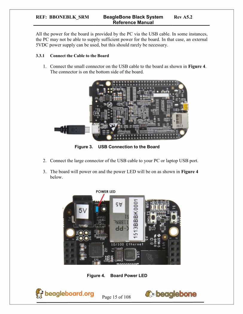
REF: BBONEBLK_SRM BeagleBone Black System Reference Manual
Rev A5.2
Page 15 of 108
All the power for the board is provided by the PC via the USB cable. In some instances, the PC may not be able to supply sufficient power for the board. In that case, an external 5VDC power supply can be used, but this should rarely be necessary. 3.3.1 Connect the Cable to the Board
1. Connect the small connector on the USB cable to the board as shown in Figure 4.
The connector is on the bottom side of the board.
Figure 3. USB Connection to the Board
2. Connect the large connector of the USB cable to your PC or laptop USB port.
3. The board will power on and the power LED will be on as shown in Figure 4 below.
Figure 4. Board Power LED
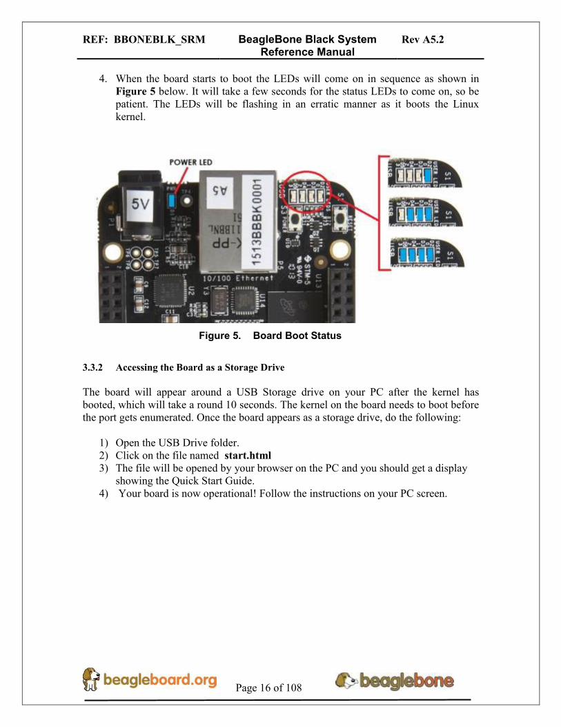
REF: BBONEBLK_SRM BeagleBone Black System Reference Manual
Rev A5.2
Page 16 of 108
4. When the board starts to boot the LEDs will come on in sequence as shown in Figure 5 below. It will take a few seconds for the status LEDs to come on, so be patient. The LEDs will be flashing in an erratic manner as it boots the Linux kernel.
Figure 5. Board Boot Status
3.3.2 Accessing the Board as a Storage Drive
The board will appear around a USB Storage drive on your PC after the kernel has booted, which will take a round 10 seconds. The kernel on the board needs to boot before the port gets enumerated. Once the board appears as a storage drive, do the following:
1) Open the USB Drive folder. 2) Click on the file named start.html 3) The file will be opened by your browser on the PC and you should get a display
showing the Quick Start Guide. 4) Your board is now operational! Follow the instructions on your PC screen.
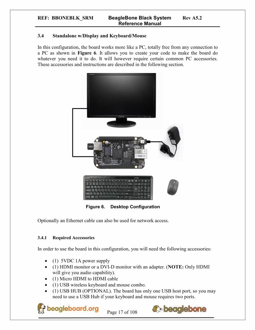
REF: BBONEBLK_SRM BeagleBone Black System Reference Manual
Rev A5.2
Page 17 of 108
3.4 Standalone w/Display and Keyboard/Mouse
In this configuration, the board works more like a PC, totally free from any connection to a PC as shown in Figure 6. It allows you to create your code to make the board do whatever you need it to do. It will however require certain common PC accessories. These accessories and instructions are described in the following section.
Figure 6. Desktop Configuration
Optionally an Ethernet cable can also be used for network access. 3.4.1 Required Accessories
In order to use the board in this configuration, you will need the following accessories:
(1) 5VDC 1A power supply
(1) HDMI monitor or a DVI-D monitor with an adapter. (NOTE: Only HDMI will give you audio capability).
(1) Micro HDMI to HDMI cable
(1) USB wireless keyboard and mouse combo.
(1) USB HUB (OPTIONAL). The board has only one USB host port, so you may need to use a USB Hub if your keyboard and mouse requires two ports.

REF: BBONEBLK_SRM BeagleBone Black System Reference Manual
Rev A5.2
Page 18 of 108
For an up-to-date list of confirmed working accessories please go to http://circuitco.com/support/index.php?title=BeagleBone_Black_Accessories 3.4.2 Connecting Up the Board
1. Connect the big end of the HDMI cable as shown in Figure 7 to your HDMI monitor. Refer to your monitor Owner’s Manual for the location of your HDMI port. If you have a DVI-D Monitor go to Step 3, otherwise proceed to Step 4.
Figure 7. Connect microHDMI Cable to the Monitor
NOTE: Do not plug in the cable to the board until after the board is powered up.
2. If you have a DVI-D monitor you must use a DVI-D to HDMI adapter in addition to your HDMI cable. An example is shown in Figure 8 below from two perspectives.
Figure 8. DVI-D to HDMI Adapter
To the Monitor
To microHDMI Cable

REF: BBONEBLK_SRM BeagleBone Black System Reference Manual
Rev A5.2
Page 19 of 108
3. If you have a single wireless keyboard and mouse combination such as seen in Figure 9 below, you need to plug the receiver in the USB host port of the board as shown in Figure 10.
Figure 9. Wireless Keyboard and Mouse Combo
Figure 10. Connect Keyboard and Mouse Receiver to the Board
If you have a wired USB keyboard requiring two USB ports, you will need a HUB similar to the ones shown in Figure 11. You may want to have more than one port for other devices. Note that the board can only supply up to 500mA, so if you plan to load it down, it will need to be externally powered.
Figure 11. Keyboard and Mouse Hubs
4. Connect the Ethernet Cable
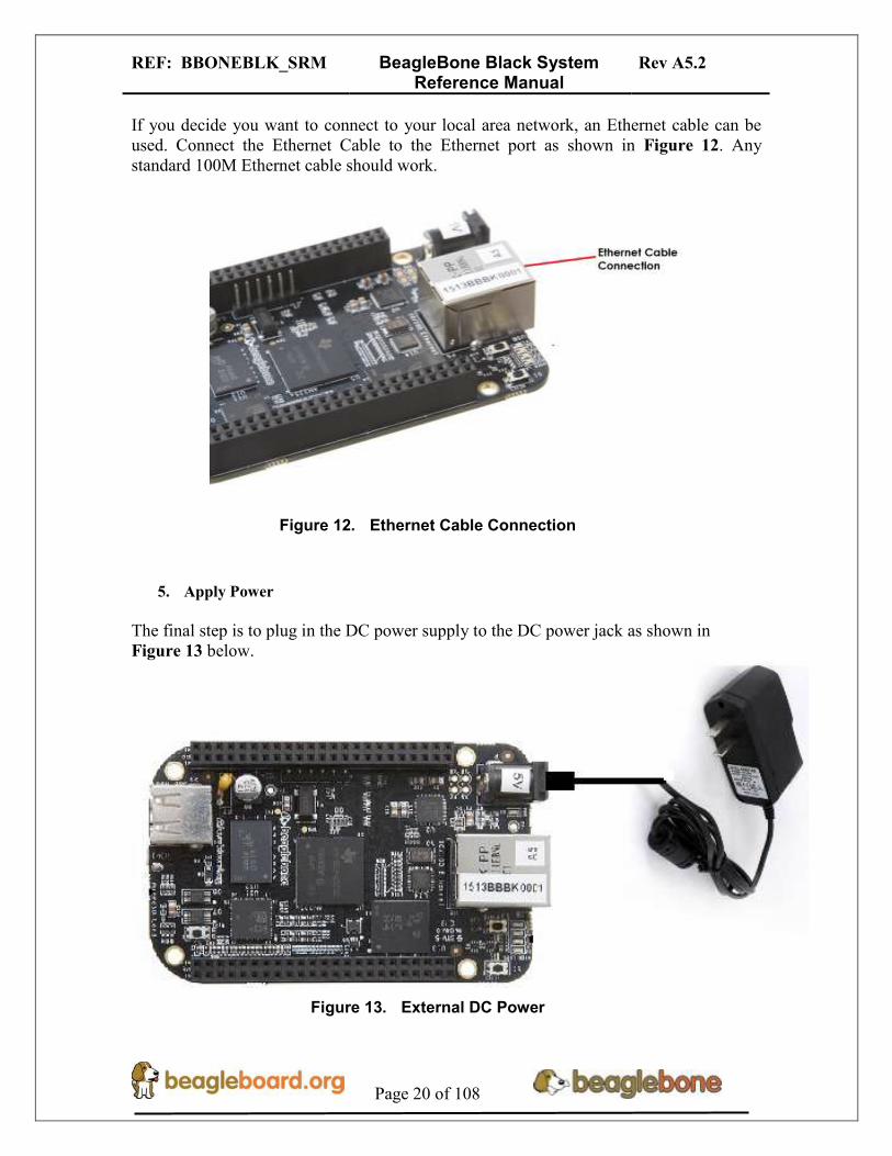
REF: BBONEBLK_SRM BeagleBone Black System Reference Manual
Rev A5.2
Page 20 of 108
If you decide you want to connect to your local area network, an Ethernet cable can be used. Connect the Ethernet Cable to the Ethernet port as shown in Figure 12. Any standard 100M Ethernet cable should work.
Figure 12. Ethernet Cable Connection
5. Apply Power
The final step is to plug in the DC power supply to the DC power jack as shown in Figure 13 below.
Figure 13. External DC Power

REF: BBONEBLK_SRM BeagleBone Black System Reference Manual
Rev A5.2
Page 21 of 108
6. The cable needed to connect to your display is a microHDMI to HDMI. Connect the microHDMI connector end to the board at this time. The connector is on the bottom side of the board as shown in Figure 14 below.
Figure 14. Connect microHDMI Cable to the Board
The connector is fairly robust, but we suggest that you not use the cable as a leash for your Beagle. Take proper care not to put too much stress on the connector or cable.
7. Booting the Board
As soon as the power is applied to the board, it will start the booting up process. When the board starts to boot the LEDs will come on in sequence as shown in Figure
15 below. It will take a few seconds for the status LEDs to come on, so be patient. The LEDs will be flashing in an erratic manner as it boots the Linux kernel.

REF: BBONEBLK_SRM BeagleBone Black System Reference Manual
Rev A5.2
Page 22 of 108
Figure 15. Board Boot Status
While the four user LEDS can be over written and used as desired, they do have specific meanings in the image that is shipped with the board once the Linux kernel has booted.
USER0 is the heartbeat indicator from the Linux kernel.
USER1 turns on when the SD card is being accessed
USER2 is an activity indicator. It turns on when the kernel is not in the idle loop.
USER3 turns on when the onboard eMMC is being accessed.
8. A Booted System
1. The board will have a mouse pointer appear on the screen as it enters the Linux boot step. You may have to move the physical mouse to get the mouse pointer to appear. The system can come up in the suspend mode with the HDMI port in a sleep mode.
2. After a minute or two a login screen will appear. You do not have to do anything at this point.
3. After a minute or two the desktop will appear. It should be similar to the one shown in Figure 16. HOWEVER, it will change from one release to the next, so do not expect your system to look exactly like the one in the figure, but it will be very similar.
4. And at this point you are ready to go! Figure 16 shows the desktop after booting.

REF: BBONEBLK_SRM BeagleBone Black System Reference Manual
Rev A5.2
Page 23 of 108
Figure 16. Desktop Screen
NOTE: At press time this is what the default screen looks like. If you see something different, do not be alarmed. It is intended. Once the final screen is finalized, this document will be updated and available for download.

REF: BBONEBLK_SRM BeagleBone Black System Reference Manual
Rev A5.2
Page 24 of 108
4.0 BeagleBone Black Overview
The BeagleBone Black is the latest addition to the BeagleBoard.org family and like its predecessors, is designed to address the Open Source Community, early adopters, and anyone interested in a low cost ARM Cortex-A8 based processor. It has been equipped with a minimum set of features to allow the user to experience the power of the processor and is not intended as a full development platform as many of the features and interfaces supplied by the processor are not accessible from the BeagleBone Black via onboard support of some interfaces. It is not a complete product designed to do any particular function. It is a foundation for experimentation and learning how to program the processor and to access the peripherals by the creation of your own software and hardware. It also offers access to many of the interfaces and allows for the use of add-on boards called capes, to add many different combinations of features. A user may also develop their own board or add their own circuitry. BeagleBone Black is manufactured and warranted by Circuitco LLC in Richardson Texas for the benefit of the community and its supporters. In addition, Circuitco provides the RMA support for the BeagleBone Black. Jason Kridner of Texas Instruments handles the community promotions and is the spokesmen for BeagleBoard.org. The board is designed by Gerald Coley, an employee of Texas Instruments and a charter member of the BeagleBoard.org community. The PCB layout was done by Circuitco and Circuitco is the sole funder of its development and transition to production. The Software is written and supported by the thousands of community members, including Jason Kridner, employees of Texas Instruments, DigiKey, and Circuitco. .

REF: BBONEBLK_SRM BeagleBone Black System Reference Manual
Rev A5.2
Page 25 of 108
4.1 BeagleBone Compatibility
The board is intended to be compatible with the original BeagleBone as much as possible. There are several areas where there are differences between the two designs. These differences are listed below, along with the reasons for the differences.
Sitara XAM3359AZCZ100, 1GHZ, processor. o Sorry, we just had to make it faster.
512MB DDR3L o Cost reduction o Performance boost o Memory size increase o Lower power
No Serial port by default. o Cost reduction o Can be added by buying a TTL to USB Cable that is widely available o Single most cost reduction action taken
No JTAG emulation over USB. o Cost reduction o JTAG header is not populated, but can easily be mounted.
Onboard Managed NAND (eMMC) o 2GB o Cost reduction o Performance boost x8 vs. x4 bits o Performance boost due to deterministic properties vs. SD card
GPMC bus may not be accessible from the expansion headers in some cases o Result of eMMC on the main board o Signals are still routed to the expansion connector o If eMMC is not used, signals can be used via expansion if eMMC is held
in reset
There may be 10 less GPIO pins available o Result of eMMC o If eMMC is not used, could still be used
The power expansion header, for battery and backlight, has been removed o Cost reduction o Space reduction o Four pins were added to provide access to the battery charger function.
HDMI interface onboard o Feature addition o Audio and video capable o Micro HDMI
No three function USB cable o Cost reduction

REF: BBONEBLK_SRM BeagleBone Black System Reference Manual
Rev A5.2
Page 26 of 108
4.2 BeagleBone Black Features and Specification
This section covers the specifications and features of the board and provides a high level description of the major components and interfaces that make up the board. Table 2 provides a list of the features.
Table 2. BeagleBone Black Features
Feature
Processor Sitara AM3359AZCZ100
1GHz, 2000 MIPS
Graphics Engine SGX530 3D, 20M Polygons/S
SDRAM Memory 512MB DDR3L 606MHZ
Onboard Flash 2GB, 8bit Embedded MMC
PMIC TPS65217C PMIC regulator and one additional LDO.
Debug Support Optional Onboard 20-pin CTI JTAG, Serial Header
Power Source miniUSB USB or DC
Jack 5VDC External Via Expansion
Header
PCB 3.4” x 2.1” 6 layers
Indicators 1-Power, 2-Ethernet, 4-User Controllable LEDs
HS USB 2.0 Client Port Access to USB0, Client mode via miniUSB
HS USB 2.0 Host Port Access to USB1, Type A Socket, 500mA LS/FS/HS
Serial Port UART0 access via 6 pin 3.3V TTL Header. Header is populated
Ethernet 10/100, RJ45
SD/MMC Connector microSD , 3.3V
User Input Reset Button Boot Button
Power Button
Video Out 16b HDMI, 1280x1024 (MAX) 1024x768,1280x720,1440x900
w/EDID Support
Audio Via HDMI Interface, Stereo
Expansion Connectors
Power 5V, 3.3V , VDD_ADC(1.8V) 3.3V I/O on all signals
McASP0, SPI1, I2C, GPIO(65), LCD, GPMC, MMC1, MMC2, 7 AIN(1.8V MAX), 4 Timers, 3 Serial Ports, CAN0,
EHRPWM(0,2),XDMA Interrupt, Power button, Expansion Board ID (Up to 4 can be stacked)
Weight 1.4 oz (39.68 grams)
Power
Refer to Section 6.1.7

REF: BBONEBLK_SRM BeagleBone Black System Reference Manual
Rev A5.2
Page 27 of 108
4.3 Board Component Locations
This section describes the key components on the board. It provides information on their location and function. Familiarize yourself with the various components on the board. 4.3.1 Connectors, LEDs, and Switches
Figure 17 below shows the locations of the connectors, LEDs, and switches on the PCB layout of the board.
Figure 17. Connectors, LEDs and Switches
DC Power is the main DC input that accepts 5V power.
Power Button alerts the processor to initiate the power down sequence.
10/100 Ethernet is the connection to the LAN.
Serial Debug is the serial debug port.
USB Client is a miniUSB connection to a PC that can also power the board.
BOOT switch can be used to force a boot from the SD card.
There are four blue LEDS that can be used by the user.
Reset Button allows the user to reset the processor.
uSD slot is where a uSD card can be installed.
microHDMI connector is where the display is connected to.
USB Host can be connected different USB interfaces such as Wi-Fi, BT, Keyboard, etc.

REF: BBONEBLK_SRM BeagleBone Black System Reference Manual
Rev A5.2
Page 28 of 108
4.3.2 Key Components
Figure 18 below shows the locations of the key components on the PCB layout of the board.
Figure 18. Key Components
Sitara AM3359AZCZ100 is the processor for the board.
Micron 512MB DDR3L is the Dual Data Rate RAM memory.
TPS65217C PMIC provides the power rails to the various components on the board.
SMSC Ethernet PHY is the physical interface to the network.
Micron eMMC is an onboard MMC chip that holds up to 2GB of data.
HDMI Framer provides control for an HDMI or DVI-D display with an adapter.

REF: BBONEBLK_SRM BeagleBone Black System Reference Manual
Rev A5.2
Page 29 of 108
5.0 BeagleBone Black High Level Specification
This section provides the high level specification of the BeagleBone Black.
5.1 Block Diagram
Figure 19 below is the high level block diagram of the BeagleBone Black.
Figure 19. BeagleBone Black Key Components

REF: BBONEBLK_SRM BeagleBone Black System Reference Manual
Rev A5.2
Page 30 of 108
5.2 Processor
For the initial release, the board uses the Sitara XAM3359AZCZ processor in the 15x15 package. This is basically the same processor as used on the original BeagleBone. It does use the updated 2.0 revision with several fixes on this new processor as opposed to the original BeagleBone. A couple of important features from this new processor include:
1GHZ Operation
RTC fix Eventually the board will move to the Sitara AM3358BZCZ100 device once released and readily available from TI. At this time we do not have a date when this will happen. We do not expect any benefit from moving to this device and there should be no impact seen as a result of making this move,
5.3 Memory
Described in the following sections are the three memory devices found on the board. 5.3.1 512MB DDR3L
A single 256Mb x16 DDR3L 4Gb (512MB) memory device is used. The memory used is the MT41K512M16HA-125 from Micron. It will operate at a clock frequency of 303MHz yielding an effective rate of 606MHZ on the DDR3L bus allowing for 1.32GB/S of DDR3L memory bandwidth.
5.3.2 32KB EEPROM
A single 32KB EEPROM is provided on I2C0 that holds the board information. This information includes board name, serial number, and revision information. This will be the same as found on the original BeagleBone. It has a test point to allow the device to be programmed and otherwise to provide write protection when not grounded. 5.3.3 2GB Embedded MMC
A single 2GB embedded MMC (eMMC) device is on the board. The device connects to the MMC1 port of the processor, allowing for 8bit wide access. Default boot mode for the board will be MMC1 with an option to change it to MMC0 for SD card booting. MMC0 cannot be used in 8Bit mode because the lower data pins are located on the pins used by the Ethernet port. This does not interfere with SD card operation but it does make it unsuitable for use as an eMMC port if the 8 bit feature is needed. 5.3.4 MicroSD Connector
The board is equipped with a single microSD connector to act as the secondary boot source for the board and, if selected as such, can be the primary boot source. The

REF: BBONEBLK_SRM BeagleBone Black System Reference Manual
Rev A5.2
Page 31 of 108
connector will support larger capacity SD cards. The SD card is not provided with the board. Booting from MMC0 will be used to flash the eMMC in the production environment or can be used by the user to update the SW as needed. 5.3.5 Boot Modes
As mentioned earlier, there are four boot modes:
eMMC Boot…This is the default boot mode and will allow for the fastest boot time and will enable the board to boot out of the box using the pre-flashed OS image without having to purchase an SD card or an SD card writer.
SD Boot…This mode will boot from the uSD slot. This mode can be used to override what is on the eMMC device and can be used to program the eMMC when used in the manufacturing process or for field updates.
Serial Boot…This mode will use the serial port to allow downloading of the software direct. A separate USB to serial cable is required to use this port.
USB Boot…This mode supports booting over the USB port.
Software to support USB and serial boot modes is not provided by beagleboard.org.
Please contact TI for support of this feature.
A switch is provided to allow switching between the modes.
Holding the boot switch down during boot without a SD card inserted will force the boot source to be the USB port and if nothing is detected on the USB client port, it will go to the serial port for download.
Without holding the switch, the board will boot from eMMC. If it is empty, then it will try booting from the uSD slot, followed by the serial port, and then the USB port.
If you hold the boot switch down during boot, and you have a uSD card inserted with a bootable image, the board will boot form the uSD card.
5.4 Power Management
The TPS65217C power management device is used along with a separate LDO to provide power to the system. The TPS65217C version provides for the proper voltages required for the DDR3L. This is the same device as used on the original BeagleBone with the exception of the power rail configuration settings which will be changed in the internal EEPROM to the TPS65217 to support the new voltages. DDR3L requires 1.5V instead of 1.8V on the DDR2 as is the case on the original BeagleBone. The 1.8V regulator setting has been changed to 1.5V for the DDR3L. The LDO3 3.3V rail has been changed to 1.8V to support those rails on the processor. LDO4 is still 3.3V for the 3.3V rails on the processor. An external LDOTLV70233 provides the 3.3V rail for the rest of the board.

REF: BBONEBLK_SRM BeagleBone Black System Reference Manual
Rev A5.2
Page 32 of 108
5.5 PC USB Interface
The board has a miniUSB connector that connects the USB0 port to the processor. This is the same connector as used on the original BeagleBone.
5.6 Serial Debug Port
Serial debug is provided via UART0 on the processor via a single 1x6 pin header. In order to use the interface a USB to TTL adapter will be required. The header is compatible with the one provided by FTDI and can be purchased for about $12 to $20 from various sources. Signals supported are TX and RX. None of the handshake signals are supported.
5.7 USB1 Host Port
On the board is a single USB Type A female connector with full LS/FS/HS Host support that connects to USB1 on the processor. The port can provide power on/off control and up to 500mA of current at 5V. Under USB power, the board will not be able to supply the full 500mA, but should be sufficient to supply enough current for a lower power USB device supplying power between 50 to 100mA. You can use a wireless keyboard/mouse configuration or you can add a HUB for standard keyboard and mouse interfacing.
5.8 Power Sources
The board can be powered from four different sources:
A USB port on a PC
A 5VDC 1A power supply plugged into the DC connector.
A power supply with a USB connector.
Expansion connectors The USB cable is shipped with each board. This port is limited to 500mA by the Power Management IC. It is possible to change the settings in the TPS65217C to increase this current, but only after the initial boot. And, at that point the PC most likely will complain, but you can also use a dual connector USB cable to the PC to get to 1A. The power supply is not provided with the board but can be easily obtained from numerous sources. A 1A supply is sufficient to power the board, but if there is a cape plugged into the board or you have a power hungry device or hub plugged into the host port, then more current may needed from the DC supply.

REF: BBONEBLK_SRM BeagleBone Black System Reference Manual
Rev A5.2
Page 33 of 108
Power routed to the board via the expansion header could be provided from power derived on a cape. The DC supply should be well regulated and 5V +/-.25V.
5.9 Reset Button
When pressed and released, causes a reset of the board. The reset button used on the BeagleBone Black is a little larger than the one used on the original BeagleBone. It has also been moved out to the edge of the board so that it is more accessible.
5.10 Power Button
A power button is provided near the reset button close to the Ethernet connector. This button takes advantage of the input to the PMIC for power down features. While a lot of capes have a button, it was decided to add this feature to the board to insure everyone had access to some new features. These features include:
Interrupt is sent to the processor to facilitate an orderly shutdown to save files and to un-mount drives.
Provides ability to let processor put board into a sleep mode to save power.
Can alert processor to wake up from sleep mode and restore state before sleep was entered.
Allows board to enter the sleep mode, preserving the RTC clock If you hold the button down longer than 8 seconds, the board will power off if you release the button when the power LED turns off. If you continue to hold it, the board will power back up completing a power cycle.
5.11 Indicators
There are a total of five blue LEDs on the board.
One blue power LED indicates that power is applied and the power management IC is up. If this LED flashes when applying power, it means that an excess current flow was detected and the PMIC has shut down.
Four blue LEDs that can be controlled via the SW by setting GPIO pins. In addition, there are two LEDs on the RJ45 to provide Ethernet status indication. One is yellow (100M Link up if on) and the other is green (Indicating traffic when flashing).
5.12 CTI JTAG Header
A place for an optional 20 pin CTI JTAG header is provided on the board to facilitate the SW development and debugging of the board by using various JTAG emulators. This

REF: BBONEBLK_SRM BeagleBone Black System Reference Manual
Rev A5.2
Page 34 of 108
header is not supplied standard on the board. To use this, a connector will need to be soldered onto the board.
5.13 HDMI Interface
A single HDMI interface is connected to the 16 bit LCD interface on the processor. The 16b interface was used to preserve as many expansion pins as possible to allow for use by the user. The NXP TDA19988BHN is used to convert the LCD interface to HDMI and convert the audio as well. The signals are still connected to the expansion headers to enable the use of LCD expansion boards or access to other functions on the board as needed. The HDMI device does not support HDCP copy protection. Support is provided via EDID to allow the SW to identify the compatible resolutions. Currently the following resolutions are supported via the software:
1280 x 1024
1440 x 900
1024 x 768
1280 x 720
5.14 Cape Board Support
The BeagleBone Black has the ability to accept up to four expansion boards or capes that can be stacked onto the expansion headers. The word cape comes from the shape of the board as it is fitted around the Ethernet connector on the main board. This notch acts as a key to insure proper orientation of the cape. The majority of capes designed for the original BeagleBone will work on the BeagleBone Black. The two main expansion headers will be populated on the board. There are a few exceptions where certain capabilities may not be present or are limited to the BeagleBone Black. These include:
GPMC bus may NOT be available due to the use of those signals by the eMMC. If the eMMC is used for booting only and the file system is on the SD card, then these signals could be used.
Another option is to use the SD or serial boot modes and not use the eMMC.
The power expansion header is not on the BeagleBone Black so those functions are not supported.
For more information on cape support refer to Section 9.0.

REF: BBONEBLK_SRM BeagleBone Black System Reference Manual
Rev A5.2
Page 35 of 108
6.0 Detailed Hardware Design
This section provides a detailed description of the Hardware design. This can be useful for interfacing, writing drivers, or using it to help modify specifics of your own design. Figure 20 below is the high level block diagram of the board.
Figure 20. BeagleBone Black Block Diagram

REF: BBONEBLK_SRM BeagleBone Black System Reference Manual
Rev A5.2
Page 36 of 108
6.1 Power Section
Figure 21 is the high level block diagram of the power section of the board.
Figure 21. High Level Power Block Diagram
This section describes the power section of the design and all the functions performed by the TPS65217C.
6.1.1 TPS65217C PMIC
The main Power Management IC (PMIC) in the system is the TPS65217C which is a single chip power management IC consisting of a linear dual-input power path, three step-down converters, and four LDOs. The system is supplied by a USB port or DC adapter. Three high-efficiency 2.25MHz step-down converters are targeted at providing the core voltage, MPU, and memory voltage for the board. The step-down converters enter a low power mode at light load for maximum efficiency across the widest possible range of load currents. For low-noise applications the devices can be forced into fixed frequency PWM using the I2C interface. The step-down converters allow the use of small inductors and capacitors to achieve a small footprint solution size. LDO1 and LDO2 are intended to support system standby mode. In normal operation, they can support up to 100mA each. LDO3 and LDO4 can support up to 285mA each. By default only LDO1 is always ON but any rail can be configured to remain up in SLEEP state. In particular the DCDC converters can remain up in a low-power PFM mode to support processor suspend mode. The TPS65217C offers flexible power-up and
PWR_BUT
PWR_EN
Interrupt
RTC_PORZ
SYS_RESET
Power Rails
I2C0
TPS65217C
DC IN
LDO 3V3

REF: BBONEBLK_SRM BeagleBone Black System Reference Manual
Rev A5.2
Page 37 of 108
power-down sequencing and several house-keeping functions such as power-good output, pushbutton monitor, hardware reset function and temperature sensor to protect the battery. For more information on the TPS65217C, refer to http://www.ti.com/product/tps65217C.
Figure 22 is the high level block diagram of the TPS65217C.
Figure 22. TPS65217C Block Diagram

REF: BBONEBLK_SRM BeagleBone Black System Reference Manual
Rev A5.2
Page 38 of 108
6.1.2 DC Input
Figure 23 below shows how the DC input is connected to the TPS65217C.
VDD_5V
P1
PJ-200A
11
33
22
DGND
DGND
C1
10uF,10V
C2
10uF,10V
DGND
U2
TPS65217C
AC10
USB12
SYS17
SYS28
VIN_DCDC121
VIN_DCDC332
VINLDO2
LDO3_IN39
VIN_DCDC222
LDO4_IN42
USB_DC
U4
TL5209
IN2
OUT3
GND15 EN1
ADJ4
GND36
GND27
GND48
DGND
VDD_3V3A
DGND
C17
2.2uF,6.3V
Figure 23. TPS65217 DC Connection
A 5VDC supply can be used to provide power to the board. The power supply current depends on how many and what type of add-on boards are connected to the board. For typical use, a 5VDC supply rated at 1A should be sufficient. If heavier use of the expansion headers or USB host port is expected, then a higher current supply will be required. The connector used is a 2.1MM center positive x 5.5mm outer barrel. The 5VDC rail is connected to the expansion header. It is possible to power the board via the expansion headers from an add-on card. The 5VDC is also available for use by the add-on cards when the power is supplied by the 5VDC jack on the board.
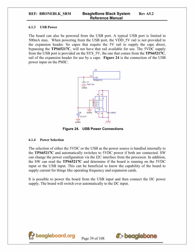
REF: BBONEBLK_SRM BeagleBone Black System Reference Manual
Rev A5.2
Page 39 of 108
6.1.3 USB Power
The board can also be powered from the USB port. A typical USB port is limited to 500mA max. When powering from the USB port, the VDD_5V rail is not provided to the expansion header. So capes that require the 5V rail to supply the cape direct, bypassing the TPS65217C, will not have that rail available for use. The 5VDC supply from the USB port is provided on the SYS_5V, the one that comes from the TPS65217C, rail of the expansion header for use by a cape. Figure 24 is the connection of the USB power input on the PMIC.
DGND
C1
10uF,10V
U2
TPS65217C
USB12
C36
0.1uf ,6.3V
DGND P4 mini USB-B
D-2 D+3
VB1
ID4
G2
7
G3
6G1
5 G5
8
G4
9
DGND
Figure 24. USB Power Connections
6.1.4 Power Selection
The selection of either the 5VDC or the USB as the power source is handled internally to the TPS65217C and automatically switches to 5VDC power if both are connected. SW can change the power configuration via the I2C interface from the processor. In addition, the SW can read the TPS65217C and determine if the board is running on the 5VDC input or the USB input. This can be beneficial to know the capability of the board to supply current for things like operating frequency and expansion cards. It is possible to power the board from the USB input and then connect the DC power supply. The board will switch over automatically to the DC input.

REF: BBONEBLK_SRM BeagleBone Black System Reference Manual
Rev A5.2
Page 40 of 108
6.1.5 Power Button
A power button is connected to the input of the TPS65217C. This is a momentary switch, the same type of switch used for reset and boot selection on the board. If you push the button the TPS65217C will send an interrupt to the processor. It is up to the processor to then pull the PMIC_EN pin low at the correct time to power down the board. At this point, the PMIC is still active, assuming that the power input was not removed. Pressing the power button will cause the board to power up again if the processor puts the board in the power off mode. In power off mode, the RTC rail is still active, keeping the RTC powered and running off the main power input. If you remove that power, then the RTC will not be powered. You also have the option of using the battery holes on the board to connect a battery if desired as discussed in the next section. If you push and hold the button for greater than 8 seconds, the PMIC will power down. But you must release the button when the power LED turns off. Holding the button past that point will cause the board to power cycle. 6.1.6 Battery Access Pads
Four pads are provided on the board to allow access to the battery pins on the TPS65217C. The pads can be loaded with a 4x4 header or you may just wire a battery into the pads. In addition they could provide access via a cape if desired. The four signals are listed below in Table 3.
Table 3. BeagleBone Black Battery Pins
PIN DESIGNATION FUNCTION
BAT TP5 Battery connection point.
SENSE TP6 Battery voltage sense input, connect to BAT directly at the battery terminal.
TS TP7 Temperature sense input. Connect to NTC thermistor to sense battery temperature.
GND TP8 System ground.
There is no fuel gauge function provide by the TPS65217C. That would need to be added if that function was required. Access to 1-wire SPI, or I2C interfaces required to use a fuel gauge will need to be accessed by using the expansion headers on the board.
NOTE: Refer to the TPS65217C documentation
before connecting anything to these pins.

REF: BBONEBLK_SRM BeagleBone Black System Reference Manual
Rev A5.2
Page 41 of 108
6.1.7 Power Consumption
The power consumption of the board varies based on power scenarios and the board boot processes. Measurements were taken with the board in the following configuration:
DC powered and USB powered
HDMI monitor connected
USB HUB
4GB Thumbdrive
Ethernet connected @ 100M
Serial debug cable connected Table 4 is an analysis of the power consumption of the board in these various scenarios.
Table 4. BeagleBone Black Power Consumption(mA@5V)
MODE USB DC DC+USB
Reset TBD TBD TBD
Idling @ UBoot 210 210 210
Kernel Booting (Peak) 460 460 460
Kernel Idling 350 350 350
Kernel Idling Display Blank 280 280 280
Loading a Webpage 430 430 430
The current will fluctuate as various activates occur, such as the LEDs on and uSD/eMMC accesses. 6.1.8 Processor Interfaces
The processor interacts with the TPS65217C via several different signals. Each of these signals is described below.
6.1.8.1 I2C0
I2C0 is the control interface between the processor and the TPS65217C. It allows the processor to control the registers inside the TPS65217C for such things as voltage scaling and switching of the input rails.
6.1.8.2 PMC_POWR_EN
On power up the VDD_RTC rail activates first. After the RTC circuitry in the processor has activated it instructs the TPS65217C to initiate a full power up cycle by activating the PMIC_POWR_EN signal by taking it HI. When powering down, the processor can take this pin low to start the power down process.

REF: BBONEBLK_SRM BeagleBone Black System Reference Manual
Rev A5.2
Page 42 of 108
6.1.8.3 LDO_GOOD
This signal connects to the RTC_PORZn signal, RTC power on reset. As the RTC circuitry comes up first, this signal indicates that the LDOs, the 1.8V VRTC rail, is up and stable. This starts the power up process.
6.1.8.4 PMIC_PGOOD
Once all the rails are up, the PMIC_PGOOD signal goes high. This releases the PORZn signal on the processor which was holding the processor reset.
6.1.8.5 WAKEUP
The WAKEUP signal from the TPS65217C is connected to the EXT_WAKEUP signal on the processor. This is used to wake up the processor when it is in a sleep mode. When an event is detected by the TPS65217C, such as the power button being pressed, it generates this signal
6.1.8.6 PMIC_INT
The PMIC_INT signal is an interrupt signal to the processor. Pressing the power button will send an interrupt to the processor allowing it to implement a power down mode in an orderly fashion, go into sleep mode, or cause it to wake up from a sleep mode. All of these require SW support.

REF: BBONEBLK_SRM BeagleBone Black System Reference Manual
Rev A5.2
Page 43 of 108
6.1.9 Power Rails
Figure 25 shows the connections of each of the rails from the TPS65217C.
Figure 25. Power Rails
6.1.9.1 VRTC Rail
The VRTC rail is a 1.8V rail that is the first rail to come up in the power sequencing. It provides power to the RTC domain on the processor and the I/O rail of the TPS65217C. It can deliver up to 250mA maximum.
6.1.9.2 VDD_3V3A Rail
The VDD_3V3A rail is supplied by the TPS65217C and provides the 3.3V for the processor rails and can provide up to 400mA.

REF: BBONEBLK_SRM BeagleBone Black System Reference Manual
Rev A5.2
Page 44 of 108
6.1.9.3 VDD_3V3B Rail
The current supplied by the VDD_3V3A rail is not sufficient to power all of the 3.3V rails on the board. So a second LDO is supplied, U4, a TL5209A, which sources the VDD_3V3B rail. It is powered up just after the VDD_3V3A rail.
6.1.9.4 VDD_1V8 Rail
The VDD_1V8 rail can deliver up to 400mA and provides the power required for the 1.8V rails on the processor and the HDMI framer. This rail is not accessible for use anywhere else on the board.
6.1.9.5 VDD_CORE Rail
The VDD_CORE rail can deliver up to 1.2A at 1.1V. This rail is not accessible for use anywhere else on the board and only connects to the processor. This rail is fixed at 1.1V and is not scaled.
6.1.9.6 VDD_MPU Rail
The VDD_MPU rail can deliver up to 1.2A. This rail is not accessible for use anywhere else on the board and only connects to the processor. This rail defaults to 1.1V and can be scaled up to allow for higher frequency operation. Changing of the voltage is set via the I2C interface from the processor.
6.1.9.7 VDDS_DDR Rail
The VDDS_DDR rail defaults to 1.5V to support the DDR3L rails and can deliver up to 1.2A. It is possible to adjust this voltage rail down to 1.35V for lower power operation of the DDR3L device. Only DDR3L devices can support this voltage setting of 1.35V.

REF: BBONEBLK_SRM BeagleBone Black System Reference Manual
Rev A5.2
Page 45 of 108
6.1.9.8 Power Sequencing
The power up process is made up of several stages and events. Figure 26 describes the events that make up the power up process for the processer.
Figure 26. Power Rail Power Up Sequencing
Figure 27 the voltage rail sequencing for the TPS65217C as it powers up and the voltages on each rail. The power sequencing starts at 15 and then goes to one. That is the way the TPS65217C is configured. You can refer to the TPS65217C datasheet for more information.
Figure 27. TPS6517C Power Sequencing Timing

REF: BBONEBLK_SRM BeagleBone Black System Reference Manual
Rev A5.2
Page 46 of 108
6.1.10 Power LED
The power LED is a blue LED that will turn on once the TPS65217C has finished the power up procedure. If you ever see the LED flash once, that means that the TPS65217C started the process and encountered an issue that caused it to shut down. The connection of the LED is shown in Figure 25. 6.1.11 TPS65217C Power Up Process
Figure 14 shows the interface between the TPS65217C and the processor.
Figure 28. Power Processor Interfaces
When voltage is applied, DC or USB, the TPS65217C connects the power to the SYS output pin which drives the switchers and LDOS in the TPS65217C. At power up all switchers and LDOs are off except for the VRTC LDO (1.8V), which provides power to the VRTC rail and controls the RTC_PORZ input pin to the processor, which starts the power up process of the processor. Once the RTC rail powers up, the RTC_PORZ pin of the processor is released. Once the RTC_PORZ reset is released, the processor starts the initialization process. After the RTC stabilizes, the processor launches the rest of the power up process by activating the PMIC_PWR_EN signal that is connected to the TPS65217C which starts the TPS65217C power up process. The LDO_PGOOD signal is provided by the TPS65217C to the processor. As this signal is 1.8V from the TPS65217C by virtue of the TPS65217C VIO rail being set to 1.8V, and the RTC_PORZ signal on the processor is 3.3V, a voltage level shifter, U4, is used. Once the LDOs and switchers are up on the TPS65217C, this signal goes active releasing the processor. The LDOs on the TPS65217C are used to power the VRTC rail on the processor.
REF: BBONEBLK_SRM BeagleBone Black System Reference Manual
Rev A5.2
Page 47 of 108
6.1.12 Processor Control Interface
Figure 11 above shows two interfaces between the processor and the TPS65217C used for control after the power up sequence has completed. The first is the I2C0 bus. This allows the processor to turn on and off rails and to set the voltage levels of each regulator to supports such things as voltage scaling. The second is the interrupt signal. This allows the TPS65217C to alert the processor when there is an event, such as when the optional power button is pressed. The interrupt is an open drain output which makes it easy to interface to 3.3V of the processor.
6.1.13 Low Power Mode Support
This section covers three general power down modes that are available. These modes are only described from a Hardware perspective as it relates to the HW design.
6.1.13.1 RTC Only
In this mode all rails are turned off except the VDD_RTC. The processor will need to turn off all the rails to enter this mode. The VDD_RTC staying on will keep the RTC active and provide for the wakeup interfaces to be active to respond to a wake up event.
6.1.13.2 RTC Plus DDR
In this mode all rails are turned off except the VDD_RTC and the VDDS_DDR, which powers the DDR3L memory. The processor will need to turn off all the rails to enter this mode. The VDD_RTC staying on will keep the RTC active and provide for the wakeup interfaces to be active to respond to a wake up event. The VDDS_DDR rail to the DDR3L is provided by the 1.5V rail of the TPS65217C and with VDDS_DDR active, the DDR3L can be placed in a self refresh mode by the processor prior to power down which allows the memory data to be saved. Currently, this feature is not included in the standard software release. The plan is to include it in future releases.
6.1.13.3 Voltage Scaling
For a mode where the lowest power is possible without going to sleep, this mode allows the voltage on the ARM processor to be lowered along with slowing the processor frequency down. The I2C0 bus is used to control the voltage scaling function in the TPS65217C.

REF: BBONEBLK_SRM BeagleBone Black System Reference Manual
Rev A5.2
Page 48 of 108
6.2 Sitara XAM3359AZCZ100 Processor
The board is designed to use either the Sitara AM3358AZCZ100 or XAM3358BZCZ100 processor in the 15 x 15 package. The initial units built will use the XAM3359AZCZ100 processor from TI. This is the same processor as used on the original BeagleBone except for a different revision. Later, we will switch to the AM3358BZCZ100 device when released. 6.2.1 Description
Figure 29 is a high level block diagram of the processor. For more information on the processor, go to http://www.ti.com/product/am3359.
Figure 29. Sitara XAM3359AZCZ Block Diagram
REF: BBONEBLK_SRM BeagleBone Black System Reference Manual
Rev A5.2
Page 49 of 108
NOTE: Figure 29 is an older block diagram and the higher frequency is not reflected. As soon an updated picture is available, this will be changed. You can also refer to the updated datasheet for the XAM3359 processor. 6.2.2 High Level Features
Table 5 below shows a few of the high level features of the Sitara processor.
Table 5. Processor Features
Operating Systems Linux, Android, Windows
Embedded CE,QNX, ThreadX
MMC/SD 3
Standby Power 7 mW CAN 2
ARM CPU 1 ARM Cortex-A8 UART (SCI) 6
ARM MHz (Max.) 275,500,600,800,1000 ADC 8-ch 12-bit
ARM MIPS (Max.) 1000,1200,2000 PWM (Ch) 3
Graphics Acceleration
1 3D eCAP 3
Other Hardware Acceleration
2 PRU-ICSS,Crypto Accelerator
eQEP 3
On-Chip L1 Cache 64 KB (ARM Cortex-A8)
RTC 1
On-Chip L2 Cache 256 KB (ARM Cortex-
A8) I2C 3
Other On-Chip Memory
128 KB McASP 2
Display Options LCD SPI 2
General Purpose Memory
1 16-bit (GPMC, NAND flash, NOR Flash, SRAM)
DMA (Ch) 64-Ch EDMA
DRAM 1 16-bit (LPDDR-400,
DDR2-532, DDR3-606) IO Supply (V)
1.8V(ADC),3.3V
USB Ports 2 Operating
Temperature Range (C)
-40 to 90
6.2.3 Documentation
Full documentation for the processor can be found on the TI website at http://www.ti.com/product/am3359 for the current processor used on the board. Make sure that you always use the latest datasheets and Technical Reference Manuals (TRM).

REF: BBONEBLK_SRM BeagleBone Black System Reference Manual
Rev A5.2
Page 50 of 108
6.3 DDR3L Memory
The BeagleBone Black uses a single MT41K256M16HA-125 512MB DDR3L device from Micron that interfaces to the processor over 16 data lines, 16 address lines, and 14 control lines. The following sections provide more details on the design. 6.3.1 Memory Device
The design will support standard DDR3 and DDR3L x16 devices. A single x16 device is used on the board and there is no support for two x8 devices. The DDR3 devices work at 1.5V and the DDR3L devices can work down to 1.35V to achieve lower power. The specific Micron device used is the MT41K256M16HA-125. It comes in a 96-BALL FBGA package with 0.8 mil pitch. Other standard DDR3 devices can also be supported, but the DDR3L is the lower power device and was chosen for its ability to work at 1.5V or 1.35V. The standard frequency that the DDR3L is run at on the board is 303MHZ. 6.3.2 DDR3L Memory Design
Figure 30 is the schematic for the DDR3L memory device. Each of the groups of signals is described in the following lines. Address Lines: Provide the row address for ACTIVATE commands, and the column address and auto pre-charge bit (A10) for READ/WRITE commands, to select one location out of the memory array in the respective bank. A10 sampled during a PRECHARGE command determines whether the PRECHARGE applies to one bank (A10 LOW, bank selected by BA[2:0]) or all banks (A10 HIGH). The address inputs also provide the op-code during a LOAD MODE command. Address inputs are referenced to VREFCA. A12/BC#: When enabled in the mode register (MR), A12 is sampled during READ and WRITE commands to determine whether burst chop (on-the-fly) will be performed (HIGH = BL8 or no burst chop, LOW = BC4 burst chop). Bank Address Lines: BA[2:0] define the bank to which an ACTIVATE, READ, WRITE, or PRECHARGE command is being applied. BA[2:0] define which mode register (MR0, MR1, MR2, or MR3) is loaded during the LOAD MODE command. BA[2:0] are referenced to VREFCA. CK and CK# Lines: are differential clock inputs. All address and control input signals are sampled on the crossing of the positive edge of CK and the negative edge of CK#. Output data strobe (DQS, DQS#) is referenced to the crossings of CK and CK#. Clock Enable Line: CKE enables (registered HIGH) and disables (registered LOW) internal circuitry and clocks on the DRAM. The specific circuitry that is enabled/disabled is dependent upon the DDR3 SDRAM configuration and operating mode. Taking CKE LOW provides PRECHARGE power-down and SELF REFRESH operations (all banks idle) or active power-down (row active in any bank). CKE is synchronous for power-down entry and exit and for self refresh entry. CKE is asynchronous for self refresh exit.

REF: BBONEBLK_SRM BeagleBone Black System Reference Manual
Rev A5.2
Page 51 of 108
Input buffers (excluding CK, CK#, CKE, RESET#, and ODT) are disabled during power-down. Input buffers (excluding CKE and RESET#) are disabled during SELF REFRESH. CKE is referenced to VREFCA.
DDR_CKE3DDR_CLKn3DDR_CLK3
DDR_WEn3DDR_CASn3DDR_RASn3DDR_CSn3
DDR_RESETn3
C124
0.1uf ,6.3V
DDR_DQM03DDR_DQM13
4Gb(512MB) DDR3L
DDR_A15
R971.5K,1%
R9610K,1%
R10010K,1%
R99240E
R9810K,1%
C123
0.001uf ,50V
DDR_ODT
U12
MT41K256M16HA -125:E
CKJ7
CKnK7
CKEK9
CSnL2
RASnJ3
CASnK3
WEnL3
A0N3
A1P7
A2P3
A3N2
A4P8
A5P2
A6R8
A7R2
A8T8
A9R3
A10L7
A11R7
A12N7
A13T3
A14T7
BA0M2
BA1N8
BA2M3
DQ0E3
DQ1F7
DQ2F2
DQ3F8
DQ4H3
DQ5H8
DQ6G2
DQ7H7
ODTK1
VSS1A9
VSS2B3
VSS3E1
VSS4G8
VSSQ4D8VSSQ3D1VSSQ2B9VSSQ1B1
VSSQ5E2
VDDQ1A1
VDDQ2A8
VDDQ3C1
VDDQ4C9
VDDQ5D2
VDD1B2
VDD2G7
UDQSnB7
UDMD3
LDME7
LDQSnG3
UDQSC7
LDQSF3
DQ8D7
DQ10C8
DQ11C2
DQ14B8
DQ12A7
DQ15A3
DQ13A2
VDD9D9
VSSQ6E8
VDDQ7E9
VDDQ8F1
VSSQ7F9
VSSQ8G1
VSSQ9G9
VREF_DQH1
VDDQ9H2
VDDQ10H9
NC1J1
NC2J9
VSS5J2
VSS6J8
VDD4K2
VDD5K8
NC3L1
ZQL8
NC4L9
VSS7M1
A15M7
VREF_CAM8
VSS8M9
VDD6N1
VDD7N9
VSS9P1
VSS10P9
VDD8R1
VDD3R9
VSS11T1
RESET#T2
VSS12T9
DQ9C3
VDDS_DDR
DGND
DGND
DGND
DDR_D10DDR_D11
VDDS_DDR
DDR_D8
DDR_D15
DDR_D13DDR_D14
DDR_D9
VDDS_DDR
DGND
DDR_D12
DGND
DDR_ODT 3
VDDS_DDR
DDR_DQS03
DDR_DQSN03
DDR_D1DDR_D2DDR_D3
DDR_DQSN13DDR_DQS13
DDR_D4
DDR_D0
DDR_D7
DDR_D5DDR_D6
DDR_A1
DDR_A3
DDR_A[15..0] 3
DDR_BA[2..0] 3
DDR_A6
DDR_A2
DDR_A8DDR_A9
DDR_A4
DDR_A0
DDR_D[15..0]3DDR_A7
DDR_A13DDR_A14
DDR_A10
DDR_A5
DDR_BA1DDR_BA2
DDR_BA0
DDR_A11DDR_A12
DDR_A[15..0]
ZQ
DDR_BA[2..0]
DDR_VREF
Figure 30. DDR3L Memory Design
Chip Select Line: CS# enables (registered LOW) and disables (registered HIGH) the command decoder. All commands are masked when CS# is registered HIGH. CS# provides for external rank selection on systems with multiple ranks. CS# is considered part of the command code. CS# is referenced to VREFCA.
REF: BBONEBLK_SRM BeagleBone Black System Reference Manual
Rev A5.2
Page 52 of 108
Input Data Mask Line: DM is an input mask signal for write data. Input data is masked when DM is sampled HIGH along with the input data during a write access. Although the DM ball is input-only, the DM loading is designed to match that of the DQ and DQS balls. DM is referenced to VREFDQ. On-die Termination Line: ODT enables (registered HIGH) and disables (registered LOW) termination resistance internal to the DDR3L SDRAM. When enabled in normal operation, ODT is only applied to each of the following balls: DQ[7:0], DQS, DQS#, and DM for the x8; DQ[3:0], DQS, DQS#, and DM for the x4. The ODT input is ignored if disabled via the LOAD MODE command. ODT is referenced to VREFCA. 6.3.3 Power Rails
The DDR3L memory device and the DDR3 rails on the processor are supplied by the TPS65217C. Default voltage is 1.5V but can be scaled down to 1.35V if desired. 6.3.4 VREF
The VREF signal is generated from a voltage divider on the VDDS_DDR rail that powers the processor DDR rail and the DDR3L device itself. Figure 31 below shows the configuration of this signal and the connection to the DDR3L memory device and the processor.
U12
MT41K256M16HA-125
VREF_DQH1
VREF_CAM8
15mm x 15mm Package
U5A
XAM3359AZCZ
VREFSSTLJ4
C124
0.1uf ,6.3V
R10010K,1%
R9810K,1%
C123
0.001uf ,50V
DGND
DDR_VREF
VDDS_DDR
DGND
DGND
C28
0.1uf ,6.3V
DDR_VREF
Figure 31. DDR3L VREF Design

REF: BBONEBLK_SRM BeagleBone Black System Reference Manual
Rev A5.2
Page 53 of 108
6.4 2GB eMMC Memory
The eMMC is a communication and mass data storage device that includes a Multi- MediaCard (MMC) interface, a NAND Flash component, and a controller on an advanced 11-signal bus, which is compliant with the MMC system specification. The nonvolatile eMMC draws no power to maintain stored data, delivers high performance across a wide range of operating temperatures, and resists shock and vibration disruption. One of the issues faced with SD cards is that across the different brands and even within the same brand, performance can vary. Cards use different controllers and different memories, all of which can have bad locations that the controller handles. But the controllers may be optimized for reads or writes. You never know what you will be getting. This can lead to varying rates of performance. The eMMC card is a known controller and when coupled with the 8bit mode, 8 bits of data instead of 4, you get double the performance which should result in quicker boot times. The following sections describe the design and device that is used on the board to implement this interface. 6.4.1 eMMC Device
The device used in a Micron MTFC2GMTEA-0F_WT 2GB eMMC device. This is a new device and so for documentation and support, you will need to contact your local Micron representative. The package is a 153 ball WFBGA device. The footprint on the BeagleBone Black for this device supports 4GB and 8GB devices. As this is a JEDEC standard, there are other suppliers that may work in this design as well. The only device that has been tested is the MTFC2GMTEA-0F_WT.

REF: BBONEBLK_SRM BeagleBone Black System Reference Manual
Rev A5.2
Page 54 of 108
6.4.2 eMMC Circuit Design
Figure 32 is the design of the eMMC circuitry. The eMMC device is connected to the MMC1 port on the processor. MMC0 is still used for the uSD card as is currently done on the original BeagleBone. The device runs at 3.3V both internally and the external I/O rails. The VCCI is an internal voltage rail to the device. The manufacturer recommends that a 1uf capacitor be attached to this rail, but a 2.2uF was chosen to provide a little margin. Pullup resistors are used to increase the rise time on the signals to compensate for any capacitance on the board.
DGND
VDD_3V3B
C125
2.2uF,6.3V
DGND
R101
10K
,1%
R102
10K
,1%
R104
10K
,1%
R103
10K
,1%
VDD_3V3B
R105
10K
,1%
R106
10K
,1%
R107
10K
,1%
R108
10K
,1%
R109
10K
,1%
R110
10K
,1%
U13
MEM_MNAND_2GB
DAT0A3
DAT1A4
DAT2A5
DAT3B2
DAT4B3
DAT5B4
DAT6B5
DAT7B6
VC
CI
C2
VS
SQ
4C
4
VC
CQ
4C
6
VC
C3
E6
VS
S2
E7
VS
S5
N5
VC
C2
F5
VS
S1
G5
VS
S3
H10
VS
S4
K8
VC
C1
K9
VC
CQ
5M
4
CMDM5
CLKM6
VS
SQ
1N
2
VC
CQ
3N
4
VC
CQ
1P
3
VS
SQ
3P
4
VC
CQ
2P
5
VS
SQ
2P
6
RSTK5
VC
C0
J10
R111
10K
,1%
U5A
AM3358_ZCZ
MMC1_CLKU9MMC1_CMDV9
MMC1_DAT0U7
MMC1_DAT1V7
MMC1_DAT2R8
MMC1_DAT3T8
MMC1_DAT4U8
MMC1_DAT5V8
MMC1_DAT6R9
MMC1_DAT7T9
GPIO2_0T13 R162
0,1%,DNI
Figure 32. eMMC Memory Design
The pins used by the eMMC1 in the boot mode are listed below in Table 6.
Table 6. eMMC Boot Pins
For eMMC devices the ROM will only support raw mode. The ROM Code reads out raw sectors from image or the booting file within the file system and boots from it. In raw mode the booting image can be located at one of the four consecutive locations in the main area: offset 0x0 / 0x20000 (128 KB) / 0x40000 (256 KB) / 0x60000 (384 KB). For this reason, a booting image shall not exceed 128KB in size. However it is possible to
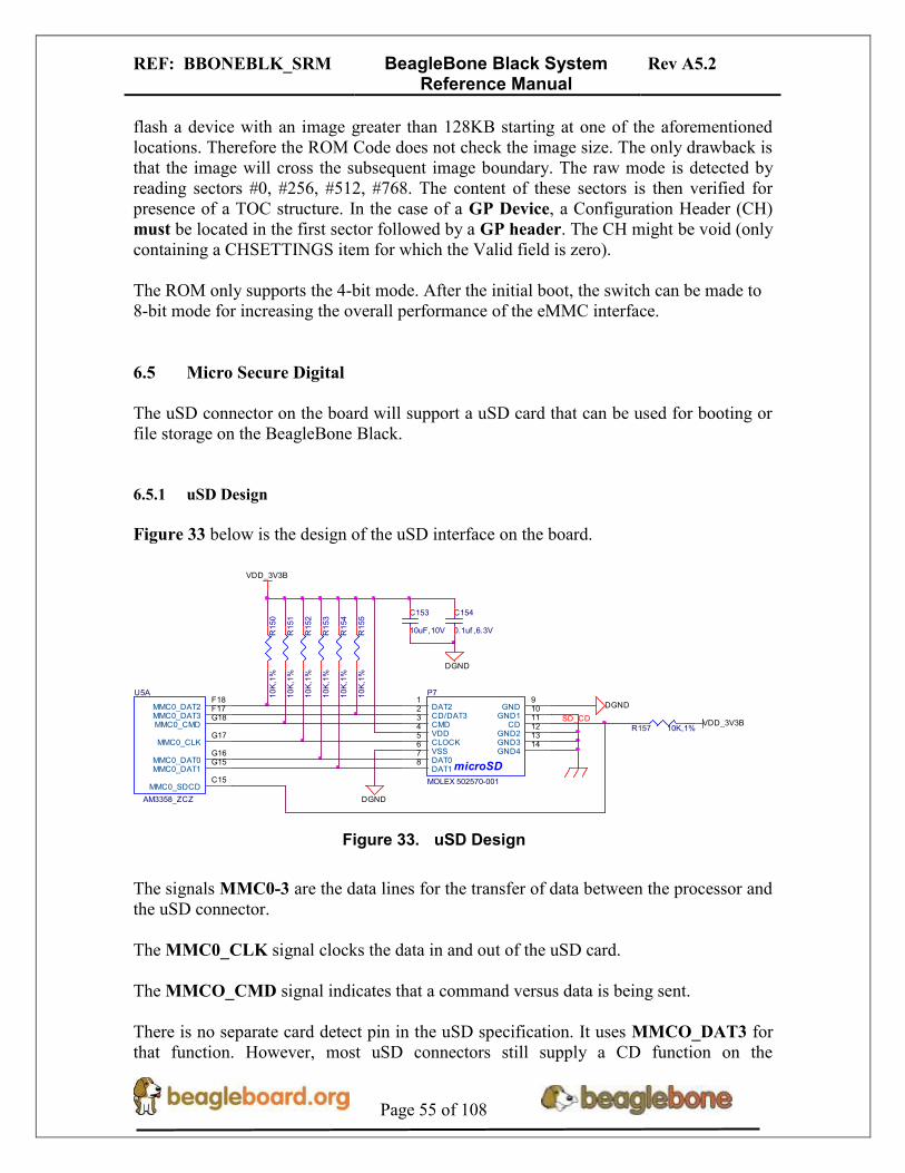
REF: BBONEBLK_SRM BeagleBone Black System Reference Manual
Rev A5.2
Page 55 of 108
flash a device with an image greater than 128KB starting at one of the aforementioned locations. Therefore the ROM Code does not check the image size. The only drawback is that the image will cross the subsequent image boundary. The raw mode is detected by reading sectors #0, #256, #512, #768. The content of these sectors is then verified for presence of a TOC structure. In the case of a GP Device, a Configuration Header (CH) must be located in the first sector followed by a GP header. The CH might be void (only containing a CHSETTINGS item for which the Valid field is zero). The ROM only supports the 4-bit mode. After the initial boot, the switch can be made to 8-bit mode for increasing the overall performance of the eMMC interface.
6.5 Micro Secure Digital
The uSD connector on the board will support a uSD card that can be used for booting or file storage on the BeagleBone Black. 6.5.1 uSD Design
Figure 33 below is the design of the uSD interface on the board.
U5A
AM3358_ZCZ
MMC0_CLKG17
MMC0_CMDG18
MMC0_DAT0G16
MMC0_DAT1G15
MMC0_DAT2F18
MMC0_DAT3F17
MMC0_SDCDC15
DGND
SD_CD
DGND
R150
10K
,1%
R153
10K
,1%
R151
10K
,1%
R157 10K,1%
R152
10K
,1%
R154
10K
,1%
R155
10K
,1%
VDD_3V3B
VDD_3V3B
DGND
C153
10uF,10V
microSD
P7
MOLEX 502570-001
DAT21
CD/DAT32
CMD3
VDD4
CLOCK5
VSS6
DAT07
DAT18
GND9
GND110
CD11
GND212
GND313
GND414
C154
0.1uf ,6.3V
Figure 33. uSD Design
The signals MMC0-3 are the data lines for the transfer of data between the processor and the uSD connector. The MMC0_CLK signal clocks the data in and out of the uSD card. The MMCO_CMD signal indicates that a command versus data is being sent. There is no separate card detect pin in the uSD specification. It uses MMCO_DAT3 for that function. However, most uSD connectors still supply a CD function on the
REF: BBONEBLK_SRM BeagleBone Black System Reference Manual
Rev A5.2
Page 56 of 108
connectors. In the BeagleBone Black design, this pin is connected to the MMC0_SDCD pin for use by the processor. You can also change the pin to GPIO0_6, which is able to wake up the processor from a sleep mode when an SD card is inserted into the connector. Pullup resistors are provided on the signals to increase the rise times of the signals to overcome PCB capacitance. Power is provided from the VDD_3V3B rail and a 10uf capacitor is provided for filtering.
6.6 User LEDs
There are four user LEDs on the BeagleBone Black. These are connected to GPIO pins on the processor. Figure 34 shows the interfaces for the user LEDs.
R76100K,1%
R77100K,1%
D2 LTST-C191TBKT
DGNDDGND
47k
10k Q1A
DMC56404
16
2 47k
10k Q1B
DMC56404
43
5
DGNDDGND
USR13
USR03
LE
DA
C
LE
DB
C
USR0
R73820,5%
R72820,5%
LE
DA
A
LE
DB
A
SYS_5V
D3 LTST-C191TBKT D4 LTST-C191TBKT D5 LTST-C191TBKT
R78100K,1% R79
100K,1%
DGND
47k
10k Q2A
DMC56404
16
2
47k
10k Q2B
DMC56404
43
5
DGND
USR23
DGNDDGND
USR33
USR1
LE
DD
C
LE
DC
C USR3USR2
R74820,5%L
ED
CA
LE
DD
A
R71820,5%
Figure 34. User LEDs
Table 7 shows the signals used to control the four LEDs from the processor.
Table 7. User LED Control Signals/Pins
LED GPIO SIGNAL PROC PIN
USR0 GPIO1_21 V15
USR1 GPIO2_22 U15
USR2 GPIO2_23 T15
USR3 GPIO2_24 V16 A logic level of “1” will cause the LEDs to turn on.
REF: BBONEBLK_SRM BeagleBone Black System Reference Manual
Rev A5.2
Page 57 of 108
6.7 Boot Configuration
The design supports two groups of boot options on the board. The user can switch between these modes via the Boot button. The primary boot source is the onboard eMMC device. By holding the Boot button, the user can force the board to boot from the uSD slot. This enables the eMMC to be overwritten when needed or to just boot an alternate image. The following sections describe how the boot configuration works. 6.7.1 Boot Configuration Design
Figure 35 shows the circuitry that is involved in the boot configuration process. On power up, these pins are read by the processor to determine the boot order. S2 is used to change the level of one bit from HI to LO which changes the boot order.
R8
01
00
K,1
%
R8
31
00
K,1
%R
84
100
K,1
%R
85
100
K,1
%
R8
71
00
K,1
%R
86
100
K,1
%
R8
91
00
K,1
%R
88
100
K,1
%
R8
21
00
K,1
%
R9
51
00
K,1
%
uSD BOOT
VDD_3V3A
SYS_BOOT10SYS_BOOT9SYS_BOOT8
SYS_BOOT15SYS_BOOT14SYS_BOOT13SYS_BOOT12SYS_BOOT11
SYS_BOOT4
SYS_BOOT2SYS_BOOT1SYS_BOOT0
SYS_BOOT7SYS_BOOT6SYS_BOOT5
SYS_BOOT3
DGND
LCD_DATA5 4,10,11LCD_DATA4 4,10,11LCD_DATA3 4,10,11
R6
51
00
K,1
%
LCD_DATA8 4,10,11LCD_DATA7 4,10,11LCD_DATA6 4,10,11
LCD_DATA11 4,10,11LCD_DATA10 4,10,11LCD_DATA9 4,10,11
LCD_DATA14 4,10,11LCD_DATA13 4,10,11LCD_DATA12 4,10,11
LCD_DATA1 4,10,11LCD_DATA0 4,10,11
LCD_DATA15 4,10,11
LCD_DATA2 4,10,11
R6
91
00
K,1
%,D
NI
R9
31
00
K,1
%,D
NI
R9
21
00
K,1
%,D
NI
S2KMR231GLFS
1 3
2 4
R6
81
00
K,1
%
R9
11
00
K,1
%,D
NI
DGND
R9
01
00
K,1
%,D
NI
R6
41
00
K,1
%,D
NI
R75 100
R7
01
00
K,1
%,D
NI
R6
31
00
K,1
%,D
NI
R5
61
00
K,1
%
R6
71
00
K,1
%R
66
100
K,1
%
R6
21
00
K,1
%,D
NI
R6
11
00
K,1
%,D
NI
R6
01
00
K,1
%,D
NI
R9
41
00
K,1
%
R5
91
00
K,1
%,D
NI
R5
81
00
K,1
%,D
NI
R5
71
00
K,1
%,D
NI
R8
11
00
K,1
%,D
NI
R5
51
00
K,1
%,D
NI
Figure 35. Processor Boot Configuration Design
It is possible to override these setting via the expansion headers. But be careful not to add too much load such that it could interfere with the operation of the HDMI interface or LCD panels. If you choose to override these settings, it is strongly recommended that you gate these signals with the SYS_RESETn signal. This insures that after coming out of reset these signals are removed from the expansion pins.

REF: BBONEBLK_SRM BeagleBone Black System Reference Manual
Rev A5.2
Page 58 of 108
6.7.2 Default Boot Options
Based on the selected option found in Figure 36 below, each of the boot sequences for each of the two settings is shown.
Figure 36. Processor Boot Configuration
The first row in Figure 36 is the default setting. On boot, the processor will look for the eMMC on the MMC1 port first, followed by the uSD slot on MMC0, USB0 and UART0. In the event there is no uSD card and the eMMC is empty, UART0 or USB0 could be used as the board source. If you have a uSD card from which you need to boot from, hold the boot button down. On boot, the processor will look for the SPIO0 port first, then uSD on the MMC0 port, followed by USB0 and UART0. In the event there is no uSD card and the eMMC is empty, USB0 or UART0 could be used as the board source.

REF: BBONEBLK_SRM BeagleBone Black System Reference Manual
Rev A5.2
Page 59 of 108
6.8 10/100 Ethernet
The BeagleBone Black is equipped with a 10/100 Ethernet interface. It uses the same PHY as is used on the original BeagleBone. The design is described in the following sections. 6.8.1 Ethernet Processor Interface
Figure 37 shows the connections between the processor and the PHY. The interface is in the MII mode of operation.
RXER/PHYAD0
RXD1/MODE1RXD0/MODE0
CRS
R131 100,1%R133 100,1%
R129 100,1%
R139 100,1%
R125 100,1%R126 100,1%
R138 100,1%
R1
19
1.5
K,5
%
R128 100,1%R127 100,1%
R134 100,1%
VDD_3V3B
RXD3/PHYAD2RXD2/RMIISEL
MODE2
TXCLK
REFCLKORXDV
U14
LAN8710A
QFN32_5X5MM_EP3P3MM
MDIO16
MDC17
RXD3/PHYAD28
RXD2/RMIISEL9
RXD1/MODE110
RXD0/MODE011
RXDV26
RXCLK/PHYAD17
RXER/RXD4/PHYAD013
TXCLK20
TXEN21
TXD022
TXD123
TXD224
TXD325
COL/CRS_DV/MODE215
CRS14
U5B
AM3358_ZCZ
GMII1_CRSH17
GMII1_TXD0K17
GMII1_TXD1K16
GMII1_TXD2K15
GMII1_TXD3J18
GMII1_TXCLKK18
GMII1_TXENJ16
GMII1_RXERRJ15
GMII1_RXDVJ17
GMII1_RXCLKL18
GMII1_RXD0M16GMII1_RXD1L15GMII1_RXD2L16GMII1_RXD3L17MDIO_CLKM18MDIO_DATAM17
GMII1_COLH16
Figure 37. Ethernet Processor Interface
This is the same interface as is used on the BeagleBone. No changes were made in this design for the board.

REF: BBONEBLK_SRM BeagleBone Black System Reference Manual
Rev A5.2
Page 60 of 108
6.8.2 Ethernet Connector Interface
The off board side of the PHY connections are shown in Figure 38 below.
ACTIVE WHEN AT 100MB
ACTIVE WHEN LINK PRESENT.BLINKS OFF DURING ACTIVITY.
GRN_C
ETH_TXD4
TXNTXP
TCT_RCT
RXPRXN
RBIAS
ESD_RING
C138
15pF,DNI
C139
15pF,DNIU14
LAN8710A
QFN32_5X5MM_EP3P3MM
RBIAS32
RXP31
RXN30
TXN28TXP29
nINT/TXER/TXD418
LED2/nINTSEL2LED1/REGOFF3
R1370,1%
C140
15pF,DNI
R136
.1,0805C141
0.022uF,10V
R13510K,1%
R14510K,1%
R120
49.9
,1%
R130 470,5%
R132 470,5%
P5
WE_7499010211A
TCT5
TD+3
TD-6
RD+1
RD-2
RCT4
YELC11
YELA12
GRNC10
GRNA9
GND8
SHD113
SHD214
NC7
R121
49.9
,1%
R122
49.9
,1%
R14412.1K,1%
R123
49.9
,1%
C137
15pF,DNI
VDD_PHYA
DGND
DGND
DGND
DGND
VDD_PHYA
DGND DGNDDGND DGND
DGND
DGND
DGND
YELA
GRNA
YEL_C
Figure 38. Ethernet Connector Interface
This is the same interface as is used on the BeagleBone. No changes were made in this design for the board.

REF: BBONEBLK_SRM BeagleBone Black System Reference Manual
Rev A5.2
Page 61 of 108
Ethernet PHY Power, Reset, and Clocks
Figure 39 show the power, reset, and lock connections to the LAN8710A PHY. Each of these areas is discussed in more detail in the following sections.
PHY_VDDCR
PHY_XTAL2
PHY_XTAL1
PHYX
REFCLKO
C1350.1uf ,6.3V
C1310.1uf ,6.3V
C1320.1uf ,6.3V
R131 100,1%
R142 0,1%
FB4150OHM800mA
1 2
R14310,1%
C143
30pF,50V
U14
LAN8710A
nRST19
XTAL1/CLKIN5
XTAL24
GN
D_E
P33
VD
DIO
12
VD
D1A
27
VD
D2A
1
VD
DC
R6
RXCLK/PHYAD17
R140 0,1%,DNI
C1341uF,10V
C142
30pF,50V
Y3
25.000MHzXTAL150SMD_125X196
12
C136470pF,6.3V
R124 10,1%,DNI
R1411M,1%,DNI
DGND
VDD_PHYA
VDD_3V3B
DGND
DGND
DGNDDGND
DGND
DGND
DGND
SYS_RESETn3,11
RMII1_REFCLK4
C133
10uF,10V
RCLKIN
Figure 39. Ethernet PHY, Power, Reset, and Clocks
6.8.2.1 VDD_3V3B Rail
The VDD_3V3B rail is the main power rail for the LAN8710A. It originates at the VD_3V3B regulator and is the primary rail that supports all of the peripherals on the board. This rail also supplies the VDDIO rails which set the voltage levels for all of the I/O signals between the processor and the LAN8710A.
6.8.2.2 VDD_PHYA Rail
A filtered version of VDD_3V3B rail is connected to the VDD rails of the LAN8710 and the termination resistors on the Ethernet signals. It is labeled as VDD_PHYA. The filtering inductor helps block transients that may be seen on the VDD_3V3B rail.

REF: BBONEBLK_SRM BeagleBone Black System Reference Manual
Rev A5.2
Page 62 of 108
6.8.2.3 PHY_VDDCR Rail
The PHY_VDDCR rail originates inside the LAN8710A. Filter and bypass capacitors are used to filter the rail. Only circuitry inside the LAN8710A uses this rail.
6.8.2.4 SYS_RESET
The reset of the LAN8710A is controlled via the SYS_RESETn signal, the main board reset line.
6.8.2.5 Clock Signals
A crystal is used to create the clock for the LAN8710A. The processor uses the RMII_RXCLK signal to provide the clocking for the data between the processor and the LAN8710A.
6.8.3 LAN8710A Mode Pins
There are mode pins on the LAN8710A that sets the operational mode for the PHY when coming out of reset. These signals are also used to communicate between the processor and the LAN8710A. As a result, these signals can be driven by the processor which can cause the PHY not to be initiated correctly. To insure that this does not happen, three low value pull up resistors are used. Figure 40 below shows the three mode pin resistors.
MODE2
RXD1/MODE1
RXD0/MODE0
R114
1.5
K,1
%
R112
1.5
K,1
%
R113
1.5
K,1
%
VDD_3V3B
Figure 40. Ethernet PHY Mode Pins
This will set the mode to be 111, which enables all modes and enables auto-negotiation. This design

REF: BBONEBLK_SRM BeagleBone Black System Reference Manual
Rev A5.2
Page 63 of 108
6.9 HDMI Interface
The BeagleBone Black has an onboard HDMI framer that converts the LCD signals and audio signals to drive a HDMI monitor. The design uses an NXP TDA199988 HDMI Framer. The following sections provide more detail into the design of this interface. 6.9.1 Supported Resolutions
The maximum resolution supported by the BeagleBone Black is 1280x1024 @ 60Hz. Table 8 below shows the supported resolutions. Not all resolutions may work on all monitors, but these have been tested and shown to work on at least one monitor. EDID is supported on the BeagleBone Black. Based on the EDID reading from the connected monitor, the highest compatible resolution is selected.
Table 8. HDMI Supported Monitor Resolutions
800 x 600 @60Hz 1024 x 768 @75Hz 1280 x 720 @60
800 x 600 @56Hz 1024 x 768 @70Hz
640 x 480 @75Hz 1024 x 768 @60Hz
640 x 480 @60Hz 800 x 600 @75Hz
720 x 400 @70Hz 800 x 600 @72Hz
1280 x 1024 @75Hz 720 x 480 @60Hz
6.9.2 HDMI Framer
The TDA19988 is a High-Definition Multimedia Interface (HDMI) 1.4a transmitter. It is backward compatible with DVI 1.0 and can be connected to any DVI 1.0 or HDMI sink. The HDCP mode is not used in the design. The non-HDCP version of the device is used in the BeagleBone Black design. This device provides additional embedded features like CEC (Consumer Electronic Control). CEC is a single bidirectional bus that transmits CEC over the home appliance network connected through this bus. This eliminates the need of any additional device to handle this feature. While this feature is supported in this device, as of this point, the SW to support this feature has not been implemented and is not a feature that is considered critical. It can be switched to very low power Standby or Sleep modes to save power when HDMI is not used. TDA19988 embeds I2C-bus master interface for DDC-bus communication to read EDID. This device can be controlled or configured via I2C-bus interface.

REF: BBONEBLK_SRM BeagleBone Black System Reference Manual
Rev A5.2
Page 64 of 108
6.9.3 HDMI Video Processor Interface
The Figure 41 shows the connections between the processor and the HDMI framer device. There are 16 bits of display data, 5-6-5 that is used to drive the framer. The reason for 16 bits is that allows for compatibility with display and LCD capes already available on the original BeagleBone. The unused bits on the TDA19988 are tied low. In addition to the data signals are the VSYNC, HSYNC, DE, and PCLK signals that round out the video interface from the processor.
DATA_OUT
WORD_SYNC
SCLK
DGND
U5B
AM3358_ZCZ
LCD_DATA0R1
LCD_DATA1R2
LCD_DATA2R3
LCD_DATA3R4
LCD_DATA4T1
LCD_DATA5T2
LCD_DATA6T3
LCD_DATA7T4
LCD_DATA8U1
LCD_DATA9U2
LCD_DATA10U3
LCD_DATA11U4
LCD_DATA12V2
LCD_DATA13V3
LCD_DATA14V4
LCD_DATA15T5
LCD_PCLKV5
LCD_VSYNCU5
LCD_HSYNCR5
LCD_AC_BIAS_ENR6
I2C0_SCLC16I2C0_SDAC17
GPIO1_25U16
SPI1_SCLKA13
SPI1_CS0C12
SPI1_D0B13
CLKOUT1A15
R35 33,0201R34 33,0201
R36 33,0201R37 33,0201R38 33,0201R39 33,0201
R40 33,0201R41 33,0201R42 33,0201R43 33,0201R44 33,0201
R45 33,0201
R46 33,0201R47 33,0201R48 33,0201
R30 33,0201
R32 33,0201R31 33,0201
R33 33,0201
R29 33,0201
12MHZ_SRC
U6
SN74AUC1G74
CLK1
D2
Q3
GND4
Q5CLR6PRE7VCC8
VDD_3V3A
DGND
DGND
R21 33,0201
C27
0.1uf ,6.3V
R158 10K,1%VDD_3V3B
RE
DG
RN
BL
UE
G7
G0
B7
B0
R0
R7
U11
TDA19988
VPA063
VPA162
VPA261
VPA360
VPA459
VPA558
VPA657
VPA756
VPB09
VPB18
VPB27
VPB36
VPB43
VPB52
VPB61
VPB764
VPC018
VPC117
VPC216
VPC315
VPC413
VPC512
VPC611
VPC710
VSYNC/VREF21
HSYNC/VREF22
DE/VREF20
CSCL52 CSDA51
INT50
PCLK4
ACLK23
AP024 AP125 AP226
A0_I2C53
A1_I2C54
OSC_IN27
AP328
Figure 41. HDMI Framer Processor Interface

REF: BBONEBLK_SRM BeagleBone Black System Reference Manual
Rev A5.2
Page 65 of 108
6.9.4 HDMI Control Processor Interface
In order to use the TDA19988, the processor needs to setup the device. This is done via the I2C interface between the processor and the TDA19988. There are two signals on the TDA19988 that could be used to set the address of the TDA19988. In this design they are both tied low. The I2C interface supports both 400kHz and 100KhZ operation. Table 9 shows the I2C address.
Table 9. TDA19988 I2C Address
6.9.5 Interrupt Signal
There is a HDMI_INT signal that connects from the TDA19988 to the processor. This signal can be used to alert the processor in a state change on the HDMI interface. 6.9.6 Audio Interface
There is an I2S audio interface between the processor and the TDA19988. Stereo audio can be transported over the HDMI interface to an audio equipped display. In order to create the required clock frequencies, and external 24.576MHz oscillator, Y4, is used. From this clock, the processor generates the required clock frequencies for the TDA19988. There are three signals used to pass data from the processor to the TDA19988. SCLK is the serial clock. SPI1_CS0 is the data pin to the TDA19888. SPI1_D0 is the word sync pin. These signals are configured as I2S interfaces.
REF: BBONEBLK_SRM BeagleBone Black System Reference Manual
Rev A5.2
Page 66 of 108
6.9.7 Power Connections
Figure 42 shows the power connections to the TDA19988 device. All voltage rails for the device are at 1.8V. A filter is provided to minimize any noise from the 1.8V rail getting back into the device.
FB5
150OHM800mA
1 2
HDMI_1V8
DGND
U11
TDA19988
VDDIOA(1.8V)14
VPP19TEST49
VDDA(PLL0)(1.8V)47
VDDA0(1.8V)35
VDDA1(TX)(1.8V)36
VDDDC0(1.8V)5
VDDDC1(1.8V)29
VDDA2(TX)(1.8V)41
VDDA3(TX)(1.8V)46
VDDA(PLL1)(1.8V)48
VDDIOB(1.8V)55
PAD65
C1
49
0.1
uf,
6.3
V
C1
45
0.1
uf,
6.3
V
C1
50
0.1
uf,
6.3
V
C1
47
0.1
uf,
6.3
V
C1
51
2.2
uF
,6.3
V
VDD_1V8
C1
48
2.2
uF
,6.3
V
C1
46
2.2
uF
,6.3
V
C1
44
2.2
uF
,6.3
V
R149
0,1%
Figure 42. HDMI Power Connections
All of the interfaces between the processor and the TDA19988 are 3.3V tolerant allowing for direct connection.

REF: BBONEBLK_SRM BeagleBone Black System Reference Manual
Rev A5.2
Page 67 of 108
6.9.8 HDMI Connector Interface
Figure 43 shows the design of the interface between the HDMI Framer and the connector.
HDMI_TX2+HDMI_TX2-
HDMI_CEC
HDMI_HPD
HDMI_DSDAHDMI_DSCL
R146
1.5
K,5
%
DVI_+5V
R147
1.5
K,5
%
DVI_+5V
HDMI_DSDAHDMI_DSCL
HDMI_CECHDMI_HPD
R148 10K,1% DGNDHDMI_SWING
U11
TDA19988
DSCL33
DSDA32
HPD31
CEC30
TXC+38
TXC-37
TX0+40TX0-39
TX1+43TX1-42
TX2+45TX2-44
EXT_SWING34
3 8
1 2 4 5 D7
IP4283C
Z10-T
T
3 8
1 2 4 5D6
IP4283C
Z10-T
T
P6
microHDMI
DAT2+3 DAT2-5
DAT2_S4
DAT1+6
DAT1_S7
DAT1-8
DAT0+9
DAT0_S10
DAT0-11
CLK+12
CLK-14
CLK_S13 CEC15
NC2
SCL17
SDA18
DDC/CEC GND16 +5V19
HPLG1
MTG120
MTG221
MTG322
MTG423
t
RT1PTC_RXEF010
SYS_5V
DGND
DGNDDGND
HDMI_TX0+
HDMI_TX1-
HDMI_TXC-HDMI_TXC+
HDMI_TX0-
HDMI_TX1+
Figure 43. Connector Interface Circuitry
The connector for the HDMI interface is a microHDMI. It should be noted that this connector has a different pinout than the standard or mini HDMI connectors. D6 and D7 are ESD protection devices.

REF: BBONEBLK_SRM BeagleBone Black System Reference Manual
Rev A5.2
Page 68 of 108
7.0 Connectors
This section describes each of the connectors on the board.
7.1 Expansion Connectors
The expansion interface on the board is comprised of two 46 pin connectors. All signals on the expansion headers are 3.3V unless otherwise indicated.
NOTE: Do not connect 5V logic level signals to these pins or the board will be
damaged. Figure 44 shows the location of the expansion connectors.
Figure 44. Expansion Connector Location
The location and spacing of the expansion headers are the same as on the original BeagleBone.

REF: BBONEBLK_SRM BeagleBone Black System Reference Manual
Rev A5.2
Page 69 of 108
7.1.1 Connector P8
Table 10 shows the pinout of the P8 expansion header. Other signals can be connected to this connector based on setting the pin mux on the processor, but this is the default settings on power up. The SW is responsible for setting the default function of each pin. There are some signals that have not been listed here. Refer to the processor documentation for more information on these pins and detailed descriptions of all of the pins listed. In some cases there may not be enough signals to complete a group of signals that may be required to implement a total interface. The PROC column is the pin number on the processor. The PIN column is the pin number on the expansion header. The MODE columns are the mode setting for each pin. Setting each mode to align with the mode column will give that function on that pin.

REF: BBONEBLK_SRM BeagleBone Black System Reference Manual
Rev A5.2
Page 70 of 108
Table 10. Expansion Header P8 Pinout
PIN PROC NAME MODE0 MODE1 MODE2 MODE3 MODE4 MODE5 MODE6 MODE7
1,2 GND
3 R9 GPIO1_6 gpmc_ad6 mmc1_dat6 gpio1[6]
4 T9 GPIO1_7 gpmc_ad7 mmc1_dat7 gpio1[7]
5 R8 GPIO1_2 gpmc_ad2 mmc1_dat2 gpio1[2]
6 T8 GPIO1_3 gpmc_ad3 mmc1_dat3 gpio1[3]
7 R7 TIMER4 gpmc_advn_ale timer4 gpio2[2]
8 T7 TIMER7 gpmc_oen_ren timer7 gpio2[3]
9 T6 TIMER5 gpmc_be0n_cle timer5 gpio2[5]
10 U6 TIMER6 gpmc_wen timer6 gpio2[4]
11 R12 GPIO1_13 gpmc_ad13 lcd_data18 mmc1_dat5 mmc2_dat1 eQEP2B_in gpio1[13]
12 T12 GPIO1_12 GPMC_AD12 LCD_DATA19 Mmc1_dat4 MMC2_DAT0 EQEP2A_IN gpio1[12]
13 T10 EHRPWM2B gpmc_ad9 lcd_data22 mmc1_dat1 mmc2_dat5 ehrpwm2B gpio0[23]
14 T11 GPIO0_26 gpmc_ad10 lcd_data21 mmc1_dat2 mmc2_dat6 ehrpwm2_tripzone_in gpio0[26]
15 U13 GPIO1_15 gpmc_ad15 lcd_data16 mmc1_dat7 mmc2_dat3 eQEP2_strobe gpio1[15]
16 V13 GPIO1_14 gpmc_ad14 lcd_data17 mmc1_dat6 mmc2_dat2 eQEP2_index gpio1[14]
17 U12 GPIO0_27 gpmc_ad11 lcd_data20 mmc1_dat3 mmc2_dat7 ehrpwm0_synco gpio0[27]
18 V12 GPIO2_1 gpmc_clk_mux0 lcd_memory_clk gpmc_wait1 mmc2_clk mcasp0_fsr gpio2[1]
19 U10 EHRPWM2A gpmc_ad8 lcd_data23 mmc1_dat0 mmc2_dat4 ehrpwm2A gpio0[22]
20 V9 GPIO1_31 gpmc_csn2 gpmc_be1n mmc1_cmd gpio1[31]
21 U9 GPIO1_30 gpmc_csn1 gpmc_clk mmc1_clk gpio1[30]
22 V8 GPIO1_5 gpmc_ad5 mmc1_dat5
gpio1[5]
23 U8 GPIO1_4 gpmc_ad4 mmc1_dat4 gpio1[4]
24 V7 GPIO1_1 gpmc_ad1 mmc1_dat1 gpio1[1]
25 U7 GPIO1_0 gpmc_ad0 mmc1_dat0 gpio1[0]
26 V6 GPIO1_29 gpmc_csn0 gpio1[29]
27 U5 GPIO2_22 lcd_vsync gpmc_a8 gpio2[22]
28 V5 GPIO2_24 lcd_pclk gpmc_a10 gpio2[24]
29 R5 GPIO2_23 lcd_hsync gpmc_a9 gpio2[23]
30 R6 GPIO2_25 lcd_ac_bias_en gpmc_a11 gpio2[25]
31 V4 UART5_CTSN lcd_data14 gpmc_a18 eQEP1_index mcasp0_axr1 uart5_rxd uart5_ctsn gpio0[10]
32 T5 UART5_RTSN lcd_data15 gpmc_a19 eQEP1_strobe mcasp0_ahclkx mcasp0_axr3 uart5_rtsn gpio0[11]
33 V3 UART4_RTSN lcd_data13 gpmc_a17 eQEP1B_in mcasp0_fsr mcasp0_axr3 uart4_rtsn gpio0[9]
34 U4 UART3_RTSN lcd_data11 gpmc_a15 ehrpwm1B mcasp0_ahclkr mcasp0_axr2 uart3_rtsn gpio2[17]
35 V2 UART4_CTSN lcd_data12 gpmc_a16 eQEP1A_in mcasp0_aclkr mcasp0_axr2 uart4_ctsn gpio0[8]
36 U3 UART3_CTSN lcd_data10 gpmc_a14 ehrpwm1A mcasp0_axr0 uart3_ctsn gpio2[16]
37 U1 UART5_TXD lcd_data8 gpmc_a12 ehrpwm1_tripzone_in mcasp0_aclkx uart5_txd uart2_ctsn gpio2[14]
38 U2 UART5_RXD lcd_data9 gpmc_a13 ehrpwm0_synco mcasp0_fsx uart5_rxd uart2_rtsn gpio2[15]
39 T3 GPIO2_12 lcd_data6 gpmc_a6 eQEP2_index gpio2[12]
40 T4 GPIO2_13 lcd_data7 gpmc_a7 eQEP2_strobe pr1_edio_data_out7 gpio2[13]
41 T1 GPIO2_10 lcd_data4 gpmc_a4 eQEP2A_in gpio2[10]
42 T2 GPIO2_11 lcd_data5 gpmc_a5 eQEP2B_in gpio2[11]
43 R3 GPIO2_8 lcd_data2 gpmc_a2 ehrpwm2_tripzone_in gpio2[8]
44 R4 GPIO2_9 lcd_data3 gpmc_a3 ehrpwm0_synco gpio2[9]
45 R1 GPIO2_6 lcd_data0 gpmc_a0 ehrpwm2A gpio2[6]
46 R2 GPIO2_7 lcd_data1 gpmc_a1 ehrpwm2B gpio2[7]

REF: BBONEBLK_SRM BeagleBone Black System Reference Manual
Rev A5.2
Page 71 of 108
7.1.2 Connector P9
Table 11 lists the signals on connector P9. Other signals can be connected to this connector based on setting the pin mux on the processor, but this is the default settings on power up. There are some signals that have not been listed here. Refer to the processor documentation for more information on these pins and detailed descriptions of all of the pins listed. In some cases there may not be enough signals to complete a group of signals that may be required to implement a total interface. The PROC column is the pin number on the processor. The PIN column is the pin number on the expansion header. The MODE columns are the mode setting for each pin. Setting each mode to align with the mode column will give that function on that pin. NOTES: In the table are the following notations:
PWR_BUT is a 5V level as pulled up internally by the TPS65217C. It is activated by pulling the signal to GND. # Both of these signals connect to pin 41 of P11. Resistors are installed that allow for the GPIO3_20 connection to be removed by removing R221. The intent is to allow the SW to use either of these signals, one or the other, on pin 41. SW should set the unused pin in input mode when using the other pin. This allowed us to get an extra signal out to the expansion header. @ Both of these signals connect to pin 42 of P11. Resistors are installed that allow for the GPIO3_18 connection to be removed by removing R202. The intent is to allow the SW to use either of these signals, on pin 42. SW should set the unused pin in input mode when using the other pin. This allowed us to get an extra signal out to the expansion header.
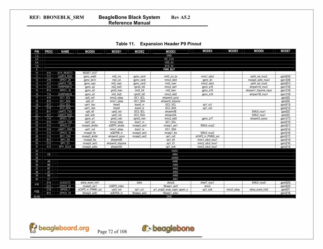
REF: BBONEBLK_SRM BeagleBone Black System Reference Manual
Rev A5.2
Page 72 of 108
Table 11. Expansion Header P9 Pinout
PIN PROC NAME MODE0 MODE1 MODE2 MODE3 MODE4 MODE5 MODE6 MODE7
1,2 GND
3,4 DC_3.3V
5,6 VDD_5V
7,8 SYS_5V
9 PWR_BUT
10 A10 SYS_RESETn RESET_OUT
11 T17 UART4_RXD gpmc_wait0 mii2_crs gpmc_csn4 rmii2_crs_dv mmc1_sdcd uart4_rxd_mux2 gpio0[30]
12 U18 GPIO1_28 gpmc_be1n mii2_col gpmc_csn6 mmc2_dat3 gpmc_dir mcasp0_aclkr_mux3 gpio1[28]
13 U17 UART4_TXD gpmc_wpn mii2_rxerr gpmc_csn5 rmii2_rxerr mmc2_sdcd uart4_txd_mux2 gpio0[31]
14 U14 EHRPWM1A gpmc_a2 mii2_txd3 rgmii2_td3 mmc2_dat1 gpmc_a18 ehrpwm1A_mux1 gpio1[18]
15 R13 GPIO1_16 gpmc_a0 gmii2_txen rmii2_tctl mii2_txen gpmc_a16 ehrpwm1_tripzone_input gpio1[16]
16 T14 EHRPWM1B gpmc_a3 mii2_txd2 rgmii2_td2 mmc2_dat2 gpmc_a19 ehrpwm1B_mux1 gpio1[19]
17 A16 I2C1_SCL spi0_cs0 mmc2_sdwp I2C1_SCL ehrpwm0_synci gpio0[5]
18 B16 I2C1_SDA spi0_d1 mmc1_sdwp I2C1_SDA ehrpwm0_tripzone gpio0[4]
19 D17 I2C2_SCL uart1_rtsn timer5 dcan0_rx I2C2_SCL spi1_cs1 gpio0[13]
20 D18 I2C2_SDA uart1_ctsn timer6 dcan0_tx I2C2_SDA spi1_cs0 gpio0[12]
21 B17 UART2_TXD spi0_d0 uart2_txd I2C2_SCL ehrpwm0B EMU3_mux1 gpio0[3]
22 A17 UART2_RXD spi0_sclk uart2_rxd I2C2_SDA ehrpwm0A EMU2_mux1 gpio0[2]
23 V14 GPIO1_17 gpmc_a1 gmii2_rxdv rgmii2_rxdv mmc2_dat0 gpmc_a17 ehrpwm0_synco gpio1[17]
24 D15 UART1_TXD uart1_txd mmc2_sdwp dcan1_rx I2C1_SCL gpio0[15]
25 A14 GPIO3_21 mcasp0_ahclkx eQEP0_strobe mcasp0_axr3 mcasp1_axr1 EMU4_mux2 gpio3[21]
26 D16 UART1_RXD uart1_rxd mmc1_sdwp dcan1_tx I2C1_SDA gpio0[14]
27 C13 GPIO3_19 mcasp0_fsr eQEP0B_in mcasp0_axr3 mcasp1_fsx EMU2_mux2 gpio3[19]
28 C12 SPI1_CS0 mcasp0_ahclkr ehrpwm0_synci mcasp0_axr2 spi1_cs0 eCAP2_in_PWM2_out gpio3[17]
29 B13 SPI1_D0 mcasp0_fsx ehrpwm0B spi1_d0 mmc1_sdcd_mux1 gpio3[15]
30 D12 SPI1_D1 mcasp0_axr0 ehrpwm0_tripzone spi1_d1 mmc2_sdcd_mux1 gpio3[16]
31 A13 SPI1_SCLK mcasp0_aclkx ehrpwm0A spi1_sclk mmc0_sdcd_mux1 gpio3[14]
32 VADC
33 C8 AIN4
34 AGND
35 A8 AIN6
36 B8 AIN5
37 B7 AIN2
38 A7 AIN3
39 B6 AIN0
40 C7 AIN1
41# D14 CLKOUT2 xdma_event_intr1 tclkin clkout2 timer7_mux1 EMU3_mux0 gpio0[20]
D13 GPIO3_20 mcasp0_axr1 eQEP0_index
Mcasp1_axr0 emu3 gpio3[20]
42@ C18 GPIO0_7 eCAP0_in_PWM0_out uart3_txd spi1_cs1 pr1_ecap0_ecap_capin_apwm_o spi1_sclk mmc0_sdwp xdma_event_intr2 gpio0[7]
B12 GPIO3_18 Mcasp0_aclkr eQEP0A_in Mcaspo_axr2 Mcasp1_aclkx gpio3[18]
43-46 GND

REF: BBONEBLK_SRM BeagleBone Black System Reference Manual
Rev A5.2
Page 73 of 108
7.2 Power Jack
The DC power jack is located next to the RJ45 Ethernet connector as shown in Figure
45. This uses the same power connector as is used on the original BeagleBone. The connector has a 2.1mm diameter center post and a 5.5mm diameter outer dimension on the barrel.
Figure 45. 5VDC Power Jack
The board requires a regulated 5VDC +/-.25V supply at 1A. A higher current rating may be needed if capes are plugged into the expansion headers.
5VDC
Power Jack
REF: BBONEBLK_SRM BeagleBone Black System Reference Manual
Rev A5.2
Page 74 of 108
7.3 USB Client
The USB Client connector is accessible on the bottom side of the board under the row of four LEDs as shown in Figure 46. It uses a 5 pin miniUSB cable, the same as is used on the original BeagleBone. The cable is provided with the board. The cable can also be used to power the board.
Figure 46. USB Client Connector
This port is a USB Client only interface and is intended for connection to a PC.
USB Client
Connector
REF: BBONEBLK_SRM BeagleBone Black System Reference Manual
Rev A5.2
Page 75 of 108
7.4 USB Host
There is a single USB Host connector on the board and is shown in Figure 47 below.
Figure 47. USB Host Connector
The port is USB 2.0 HS compatible and can supply up to 500mA of current. If more current or ports is needed, then a HUB can be used.
USB Host
Connector
REF: BBONEBLK_SRM BeagleBone Black System Reference Manual
Rev A5.2
Page 76 of 108
7.5 Serial Header
Each board has a debug serial interface that can be accessed by using a special serial cable that is plugged into the serial header as shown in Figure 48 below.
Figure 48. Serial Debug Header
Two signals are provided, TX and RX on this connector. The levels on these signals are 3.3V. In order to access these signals, a FTDI USB to Serial cable is recommended as shown in Figure 49 below.
Figure 49. FTDI USB to Serial Adapter
The cable can be purchased from several different places and must be the 3.3V version TTL-232R-3V3. Information on the cable itself can be found direct from FTDI at:
Serial Debug Connector
Pin 1
Serial Debug Cable Pin 1

REF: BBONEBLK_SRM BeagleBone Black System Reference Manual
Rev A5.2
Page 77 of 108
http://www.ftdichip.com/Support/Documents/DataSheets/Cables/DS_TTL-232R_CABLES.pdf Pin 1 of the cable is the black wire. That must align with the pin 1 on the board which is designated by the white dot on the PCB. Refer to the support WIKI http://circuitco.com/support/index.php?title=BeagleBoneBlack for more sources of this cable and other options that will work.
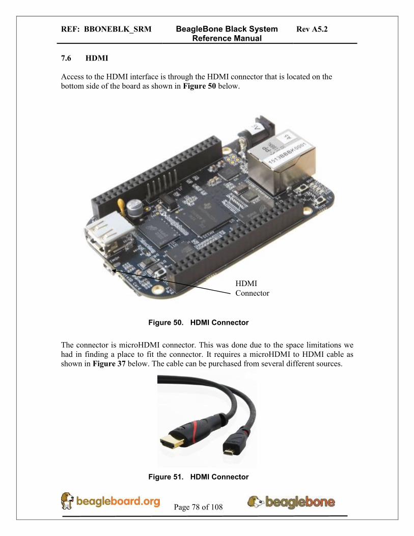
REF: BBONEBLK_SRM BeagleBone Black System Reference Manual
Rev A5.2
Page 78 of 108
7.6 HDMI
Access to the HDMI interface is through the HDMI connector that is located on the bottom side of the board as shown in Figure 50 below.
Figure 50. HDMI Connector
The connector is microHDMI connector. This was done due to the space limitations we had in finding a place to fit the connector. It requires a microHDMI to HDMI cable as shown in Figure 37 below. The cable can be purchased from several different sources.
Figure 51. HDMI Connector
HDMI
Connector

REF: BBONEBLK_SRM BeagleBone Black System Reference Manual
Rev A5.2
Page 79 of 108
7.7 microSD
A microSD connector is located on the backside of the board as shown in Figure 52 below. The SD card is not supplied with the board.
Figure 52. uSD Connector
When plugging in the SD card, the writing on the card should be up. Align the card with the connector and push to insert. Then release. There should be a click and the card will start to eject slightly, but it then should latch into the connector. To eject the card, push the SD card in and then remove your finger. The SD card will be ejected from the connector.
Do pull the SD card out or you could damage the connector.
uSD
Connector

REF: BBONEBLK_SRM BeagleBone Black System Reference Manual
Rev A5.2
Page 80 of 108
7.8 Ethernet
The board comes with a single 10/100 Ethernet interface located next to the power jack as shown in Figure 53.
Figure 53. Ethernet Connector
The PHY supports AutoMDX which means either a straight or a swap cable can be used.
10/100
Ethernet

REF: BBONEBLK_SRM BeagleBone Black System Reference Manual
Rev A5.2
Page 81 of 108
8.0 Cape Board Support
The BeagleBone Black has the ability to accept up to four expansion boards or capes that can be stacked onto the expansion headers. The word cape comes from the shape of the board as it is fitted around the Ethernet connector on the main board. This notch acts as a key to insure proper orientation of the cape. This section describes the rules for creating capes to insure proper operation with the BeagleBone Black and proper interoperability with other capes that are intended to co-exist with each other. Co-existence is not a requirement and is in itself, something that is impossible to control or administer. But, people will be able to create capes that operate with other capes that are already available based on public information as it pertains to what pins and features each cape uses. This information will be able to be read from the EEPROM on each cape. This section is intended as a guideline for those wanting to create their own capes. Its intent is not to put limits on the creation of capes and what they can do, but to set a few basic rules that will allow the SW to administer their operation with the BeagleBone Black. For this reason there is a lot of flexibility in the specification that we hope most people will find liberating and in the spirit of Open Source Hardware. I am sure there are others that would like to see tighter control, more details, more rules and much more order to the way capes are handled. Over time, this specification will change and be updated, so please refer to the latest version of this manual prior to designing your own capes to get the latest information.

REF: BBONEBLK_SRM BeagleBone Black System Reference Manual
Rev A5.2
Page 82 of 108
8.1 BeagleBoneBlack Cape Compatibility
The main expansion headers are the same between the BeagleBone and BeagleBone Black. While the pins are the same, some of these pins are now used on the BeagleBone Black. The following sections discuss these pins. The Power Expansion header was removed from the BeagleBone Black and is not available.
PAY VERY CLOSE ATTENTION TO THIS SECTION AND READ CAREFULLY!!
8.1.1 LCD Pins
The LCD pins are used on the BeagleBone Black to drive the HDMI framer. These signals are listed in Table 12 below.
Table 12. P8 LCD Conflict Pins
PIN PROC NAME MODE0
27 U5 GPIO2_22 lcd_vsync
28 V5 GPIO2_24 lcd_pclk
29 R5 GPIO2_23 lcd_hsync
30 R6 GPIO2_25 lcd_ac_bias_en
31 V4 UART5_CTSN lcd_data14
32 T5 UART5_RTSN lcd_data15
33 V3 UART4_RTSN lcd_data13
34 U4 UART3_RTSN lcd_data11
35 V2 UART4_CTSN lcd_data12
36 U3 UART3_CTSN lcd_data10
37 U1 UART5_TXD lcd_data8
38 U2 UART5_RXD lcd_data9
39 T3 GPIO2_12 lcd_data6
40 T4 GPIO2_13 lcd_data7
41 T1 GPIO2_10 lcd_data4
42 T2 GPIO2_11 lcd_data5
43 R3 GPIO2_8 lcd_data2
44 R4 GPIO2_9 lcd_data3
45 R1 GPIO2_6 lcd_data0
46 R2 GPIO2_7 lcd_data1
If you are using these pins for other functions, there are a few things to keep in mind:
On the HDMI Framer, these signals are all inputs so the framer will not be driving these pins.
The HDMI framer will add a load onto these pins.
There are small filter caps on these signals which could also change the operation of these pins if used for other functions.

REF: BBONEBLK_SRM BeagleBone Black System Reference Manual
Rev A5.2
Page 83 of 108
When used for other functions, the HDMI frame cannot be used.
There is no way to power off the framer as this would result in the framer being powered through these pins which would not a be a good idea.
In order to use these pins, the SW will need to reconfigure them to whatever function you need the pins to do. To keep power low, the HDMI framer should be put in a low power mode via the SW using the I2C interface. 8.1.2 eMMC Pins
The BeagleBone Black uses 10 pins to connect to the processor that also connect to the P8 expansion connector. These signals are listed below in Table 13.
Table 13. P8 eMMC Conflict Pins
PIN PROC NAME MODE2
11 R12 GPIO1_13 mmc1_dat5
12 T12 GPIO1_12 Mmc1_dat4
13 T10 EHRPWM2B mmc1_dat1
14 T11 GPIO0_26 mmc1_dat2
15 U13 GPIO1_15 mmc1_dat7
16 V13 GPIO1_14 mmc1_dat6
17 U12 GPIO0_27 mmc1_dat3
19 U10 EHRPWM2A mmc1_dat0
20 V9 GPIO1_31 mmc1_cmd
21 U9 GPIO1_30 mmc1_clk If using these pins, several things need to be kept in mind when doing so:
On the eMMC device, these signals are inputs and outputs.
The eMMC device will add a load onto these pins.
When used for other functions, the eMMC cannot be used. This means you must boot from the uSD slot.
If using these pins, you need to put the eMMC into reset. On power up, the eMMC is NOT reset. If you hold the Boot button down, this will force a boot from the uSD. This is not convenient when a cape is plugged into the board. There are two solutions to this issue:
1. Wipe the eMMC clean. This will cause the board to default to uSD boot. If you want to use the eMMC later, it can be reprogrammed.
2. You can also tie LCD_DATA2 low on the cape during boot. This will be the same as if you were holding the boot button. However, in order to prevent unforeseen

REF: BBONEBLK_SRM BeagleBone Black System Reference Manual
Rev A5.2
Page 84 of 108
issues, you need to gate this signal with RESET, when the data is sampled. After reset goes high, the signal should be removed from the pin.
BEFORE the SW reinitializes the pins, it MUST put the eMMC in reset. This is done by taking eMMC_RSTn (GPIO1_20) LOW. This pin does not connect to the expansion header and is accessible only on the board. DO NOT automatically drive any conflicting pin until the SW enables it. This puts the SW in control to insure that the eMMC is in reset before the signals are used from the cape.
8.2 EEPROM
Each cape must have its own EEPROM containing information that will allow the SW to identify the board and to configure the expansion headers pins as needed. The one exception is proto boards intended for prototyping. They may or may not have an EEPROM on them. An EEPROM is required for all capes sold in order for them operate correctly when plugged into the BeagleBone Black. The address of the EEPROM will be set via either jumpers or a dipswitch on each expansion board. Figure 54 below is the design of the EEPROM circuit. The EEPROM used is the same one as is used on the BeagleBone and the BeagleBone Black, a CAT24C256. The CAT24C256 is a 256 kb Serial CMOS EEPROM, internally organized as 32,768 words of 8 bits each. It features a 64−byte page write buffer and supports the Standard (100 kHz), Fast (400 kHz) and Fast−Plus (1 MHz) I2C protocol.
R128
4.7
5K
DGND
R138
4.7
5K
R142
4.7
5K VDD_3V3
VDD_3V3
R221
5.6
K,5
%R
220
5.6
K,5
%
SW1
SW DIP-2
I2C2_SDA2,4,6I2C2_SCL2,4,6
DGND
U18
CAT24C256W
A01
A12
A23
SCL6
SDA5 VCC
8
VSS4
WP7SW1_A3
SW1_A1SW1_A0
C130
0.1uF12
Figure 54. Expansion Board EEPROM Without Write Protect
The addressing of this device requires two bytes for the address which is not used on smaller size EEPROMs, which only require only one byte. Other compatible devices may

REF: BBONEBLK_SRM BeagleBone Black System Reference Manual
Rev A5.2
Page 85 of 108
be used as well. Make sure the device you select supports 16 bit addressing. The part package used is at the discretion of the cape designer. 8.2.1 EEPROM Address
In order for each cape to have a unique address, a board ID scheme is used that sets the address to be different depending on the setting of the dipswitch or jumpers on the capes. A two position dipswitch or jumpers is used to set the address pins of the EEPROM. It is the responsibility of the user to set the proper address for each board and the position in the stack that the board occupies has nothing to do with which board gets first choice on the usage of the expansion bus signals. The process for making that determination and resolving conflicts is left up to the SW and, as of this moment in time, this method is a something of a mystery due t the new Device Tree methodology introduced in the 3.8 kernel. Address line A2 is always tied high. This sets the allowable address range for the expansion cards to 0x54 to 0x57. All other I2C addresses can be used by the user in the design of their capes. But, these addresses must not be used other than for the board EEPROM information. This also allows for the inclusion of EEPROM devices on the cape if needed without interfering with this EEPROM. It requires that A2 be grounded on the EEPROM not used for cape identification. 8.2.2 I2C Bus
The EEPROMs on each expansion board are connected to I2C2 on connector P9 pins 19 and 20. For this reason I2C2 must always be left connected and should not be changed by SW to remove it from the expansion header pin mux settings. If this is done, then the system will be unable to detect the capes. The I2C signals require pullup resistors. Each board must have a 5.6K resistor on these signals. With four capes installed this will be an effective resistance of 1.4K if all capes were installed and all the resistors used were exactly 5.6K. As more capes are added the resistance is reduced to overcome capacitance added to the signals. When no capes are installed the internal pullup resistors must be activated inside the processor to prevent I2C timeouts on the I2C bus. The I2C2 bus may also be used by capes for other functions such as I/O expansion or other I2C compatible devices that do not share the same address as the cape EEPROM. 8.2.3 EEPROM Write Protect

REF: BBONEBLK_SRM BeagleBone Black System Reference Manual
Rev A5.2
Page 86 of 108
The design in Figure 55 has the write protect disabled. If the write protect is not enabled, this does expose the EEPROM to being corrupted if the I2C2 bus is used on the cape and the wrong address written to. It is recommended that a write protection function be implemented and a Test Point be added that when grounded, will allow the EEPROM to be written to. To enable write protect, Pin 7 of the EEPROM should be tied to ground. Whether or not Write Protect is provided is at the discretion of the cape designer.
Variable & MAC Memory
I2C0_SDA2,4
DGND
WP
TP2
TESTPT1
VDD_3V3B
C1020.1uf ,16V
I2C0_SCL2,4
256KX8
U7
CAT24C256W
A01
A12
A23
SCL6
SDA5 VCC
8
VSS4
WP7
DGND
R210 10K,1%
Figure 55. Expansion Board EEPROM Write Protect

REF: BBONEBLK_SRM BeagleBone Black System Reference Manual
Rev A5.2
Page 87 of 108
8.2.4 EEPROM Data Format
Table 14 shows the format of the contents of the expansion board EEPROM. Data is stored in Big Endian with the least significant value on the right. All addresses read as a single byte data from the EEPROM, but two byte addressing is used. ASCII values are intended to be easily read by the user when the EEPROM contents are dumped.
Table 14. Expansion Board EEPROM
Name Offset Size
(bytes) Contents
Header 0 4 0xAA, 0x55, 0x33, 0xEE
EEPROM Revision 4 2 Revision number of the overall format of this EEPROM in ASCII =A1
Board Name 6 32 Name of board in ASCII so user can read it when the EEPROM is dumped. Up to
developer of the board as to what they call the board..
Version 38 4 Hardware version code for board in ASCII. Version format is up to the developer.
i.e. 02.1…00A1....10A0
Manufacturer 42 16 ASCII name of the manufacturer. Company or individual’s name.
Part Number 58 16 ASCII Characters for the part number. Up to maker of the board.
Number of Pins 74 2 Number of pins used by the daughter board including the power pins used.
Decimal value of total pins 92 max, stored in HEX.
Serial Number
76
12
Serial number of the board. This is a 12 character string which is:
WWYY&&&&nnnn
where: WW = 2 digit week of the year of production
YY = 2 digit year of production
&&&&=Assembly code to let the manufacturer document the assembly number
or product. A way to quickly tell from reading the serial number what the board
is. Up to the developer to determine.
nnnn = incrementing board number for that week of production
Pin Usage
88
148
Two bytes for each configurable pins of the 74 pins on the expansion
connectors MSB LSB
Bit order: 15 14 ……………1..0
Bit 15…………..Pin is used or not……..…...0=Unused by cape 1=Used by cape
Bit 14-13………Pin Direction…………...….1 0=Output 01=Input 11=BDIR
Bits 12-7………Reserved……………………should be all zeros
Bit 6……….…..Slew Rate …………………..0=Fast 1=Slow
Bit 5…….……..Rx Enable…………………..0=Disabled 1=Enabled
Bit 4……….…..Pull Up/Dn Select…………..0=Pulldown 1=PullUp
Bit 3…………...Pull Up/DN enabled………..0=Enabled 1=Disabled
Bits 2-0 ……….Mux Mode Selection………..Mode 0-7
VDD_3V3B Current 236 2 Maximum current in milliamps. This is HEX value of the current in decimal
1500mA=0x05 0xDC 325mA=0x01 0x45
VDD_5V Current 238 2 Maximum current in milliamps. This is HEX value of the current in decimal
1500mA=0x05 0xDC 325mA=0x01 0x45
SYS_5V Current 240 2 Maximum current in milliamps. This is HEX value of the current in decimal
1500mA=0x05 0xDC 325mA=0x01 0x45
DC Supplied 242 2
Indicates whether or not the board is supplying voltage on the VDD_5V rail and
the current rating 000=No 1-0xFFFF is the current supplied storing the decimal
equivalent in HEX format
Available 244 32543 Available space for other non-volatile codes/data to be used as needed by
the manufacturer or SW driver. Could also store presets for use by SW.

REF: BBONEBLK_SRM BeagleBone Black System Reference Manual
Rev A5.2
Page 88 of 108
8.2.5 Pin Usage
Table 15 is the locations in the EEPROM to set the I/O pin usage for the cape. It contains the value to be written to the Pad Control Registers. Details on this can be found in section 9.2.2 of the AM335x Technical Reference Manual, The table is left blank as a convenience and can be printed out and used as a template for creating a custom setting for each cape. The 16 bit integers and all 16 bit fields are to be stored in Big Endian format. Bit 15 PIN USAGE is an indicator and should be a 1 if the pin is used or 0 if it is unused. Bits 14-7 RESERVED is not to be used and left as 0. Bit 6 SLEW CONTROL 0=Fast 1=Slow
Bit 5 RX Enabled 0=Disabled 1=Enabled Bit 4 PU/PD 0=Pulldown 1=Pullup. Bit 3 PULLUP/DN 0=Pullup/pulldown enabled
1= Pullup/pulldown disabled Bit 2-0 MUX MODE SELECT Mode 0-7. (refer to TRM) Refer to the TRM for proper settings of the pin MUX mode based on the signal selection to be used. The AIN0-6 pins do not have a pin mux setting, but they need to be set to indicate if each of the pins is used on the cape. Only bit 15 is used for the AIN signals.

REF: BBONEBLK_SRM BeagleBone Black System Reference Manual
Rev A5.2
Page 89 of 108
Table 15. EEPROM Pin Usage
15 14 13 12 11 10 9 8 7 6 5 4 3 2 1 0
Off
set Conn Name
Pin
Usage Type Reserved
S
L
E
W
R
X
P
U
-
P
D
P
U
/
D
E
N
Mux Mode
88 P9-22 UART2_RXD
90 P9-21 UART2_TXD
92 P9-18 I2C1_SDA
94 P9-17 I2C1_SCL
96 P9-42 GPIO0_7
98 P8-35 UART4_CTSN
100 P8-33 UART4_RTSN
102 P8-31 UART5_CTSN
104 P8-32 UART5_RTSN
106 P9-19 I2C2_SCL
108 P9-20 I2C2_SDA
110 P9-26 UART1_RXD
112 P9-24 UART1_TXD
114 P9-41 CLKOUT2
116 P8-19 EHRPWM2A
118 P8-13 EHRPWM2B
120 P8-14 GPIO0_26
122 P8-17 GPIO0_27
124 P9-11 UART4_RXD
126 P9-13 UART4_TXD
128 P8-25 GPIO1_0
130 P8-24 GPIO1_1
132 P8-5 GPIO1_2
134 P8-6 GPIO1_3
136 P8-23 GPIO1_4
138 P8-22 GPIO1_5
140 P8-3 GPIO1_6
142 P8-4 GPIO1_7
144 P8-12 GPIO1_12
146 P8-11 GPIO1_13
148 P8-16 GPIO1_14
150 P8-15 GPIO1_15
152 P9-15 GPIO1_16

REF: BBONEBLK_SRM BeagleBone Black System Reference Manual
Rev A5.2
Page 90 of 108
15 14 13 12 11 10 9 8 7 6 5 4 3 2 1 0
Off
set Conn Name
Pin
Usage Type Reserved
S
L
E
W
R
X
P
U
-
P
D
P
U
/
D
E
N
Mux Mode
154 P9-23 GPIO1_17
156 P9-14 EHRPWM1A
158 P9-16 EHRPWM1B
160 P9-12 GPIO1_28
162 P8-26 GPIO1_29
164 P8-21 GPIO1_30
166 P8-20 GPIO1_31
168 P8-18 GPIO2_1
170 P8-7 TIMER4
172 P8-9 TIMER5
174 P8-10 TIMER6
176 P8-8 TIMER7
178 P8-45 GPIO2_6
180 P8-46 GPIO2_7
182 P8-43 GPIO2_8
184 P8-44 GPIO2_9
186 P8-41 GPIO2_10
188 P8-42 GPIO2_11
190 P8-39 GPIO2_12
192 P8-40 GPIO2_13
194 P8-37 UART5_TXD
196 P8-38 UART5_RXD
198 P8-36 UART3_CTSN
200 P8-34 UART3_RTSN
202 P8-27 GPIO2_22
204 P8-29 GPIO2_23
206 P8-28 GPIO2_24
208 P8-30 GPIO2_25
210 P9-29 SPI1_D0
212 P9-30 SPI1_D1
214 P9-28 SPI1_CS0
216 P9-27 GPIO3_19
218 P9-31 SPI1_SCLK
220 P9-25 GPIO3_21

REF: BBONEBLK_SRM BeagleBone Black System Reference Manual
Rev A5.2
Page 91 of 108
15 14 13 12 11 10 9 8 7 6 5 4 3 2 1 0
Off
set Conn Name
Pin
Usage Type Reserved
S
L
E
W
R
X
P
U
-
P
D
P
U
/
D
E
N
Mux Mode
0 0 0 0 0 0 0 0 0 0 0 0 0 0 0
222 P8-39 AIN0
224 P8-40 AIN1
226 P8-37 AIN2
228 P8-38 AIN3
230 P9-33 AIN4
232 P8-36 AIN5
234 P9-35 AIN6

REF: BBONEBLK_SRM BeagleBone Black System Reference Manual
Rev A5.2
Page 92 of 108
8.3 Pin Usage Consideration
This section covers things to watch for when hooking up to certain pins on the expansion headers. 8.3.1 Boot Pins
There are 16 pins that control the boot mode of the processor that are exposed on the expansion headers. Figure 56 below shows those signals:
R80
100K
,1%
R81
100K
,1%
R82
100K
,1%
R83
100K
,1%
,DN
I
R100
42.2
K,1
%,D
NI
R101
42.2
K,1
%,D
NI
R102
42.2
K,1
%,D
NI
R103
42.2
K,1
%
R104
42.2
K,1
%,D
NI
R106
42.2
K,1
%
R107
42.2
K,1
%
R84
100K
,1%
R108
42.2
K,1
%
R110
42.2
K,1
%
R109
42.2
K,1
%
R112
42.2
K,1
%
R111
42.2
K,1
%
R114
42.2
K,1
%,D
NI
R113
42.2
K,1
%
R105
42.2
K,1
%
R115
42.2
K,1
%
R86
100K
,1%
,DN
I
R87
100K
,1%
,DN
I
R88
100K
,1%
,DN
I
R89
100K
,1%
,DN
I
R90
100K
,1%
,DN
I
VDD_3V3A
R91
100K
,1%
,DN
I
R92
100K
,1%
,DN
I
SYS_BOOT10SYS_BOOT9SYS_BOOT8
SYS_BOOT15SYS_BOOT14SYS_BOOT13SYS_BOOT12SYS_BOOT11
R93
100K
,1%
,DN
I
SYS_BOOT4
Boot Configuration
SYS_BOOT2SYS_BOOT1SYS_BOOT0
SYS_BOOT7SYS_BOOT6SYS_BOOT5
SYS_BOOT3
R94
100K
,1%
R95
100K
,1%
,DN
I
R85
100K
,1%
,DN
I
DGND
GPIO2_11 11,4GPIO2_10 11,4GPIO2_9 11,4
UART5_TXD 11,4GPIO2_13 11,4GPIO2_12 11,4
UART3_RTSN 11,4UART3_CTSN 11,4UART5_RXD 11,4
UART5_CTSN 11,4UART4_RTSN 11,4UART4_CTSN 11,4
GPIO2_7 11,4GPIO2_6 11,4
UART5_RTSN 11,4
GPIO2_8 11,4
Figure 56. Expansion Boot Pins
If you plan to use any of these signals, then on power up, these pins should not be driven. If you do, it can affect the boot mode of the processor and could keep the processor from booting or working correctly. If you are designing a cape that is intended to be used as a boot source, such as a NAND board, then you should drive the pins to reconfigure the boot mode, but only at reset. After the reset phase, the signals should not be driven to allow them to be used for the

REF: BBONEBLK_SRM BeagleBone Black System Reference Manual
Rev A5.2
Page 93 of 108
other functions found on those pins. You will need to override the resistor values in order to change the settings. The DC pull-up requirement should be based on the AM335x Vih min voltage of 2 volts and AM335x maximum input leakage current of 18uA. Also take into account any other current leakage paths on these signals which could be caused by your specific cape design. The DC pull-down requirement should be based on the AM335x Vil max voltage of 0.8 volts and AM335x maximum input leakage current of 18uA plus any other current leakage paths on these signals.
8.4 Expansion Connectors
A combination of male and female headers is used for access to the expansion headers on the main board. There are three possible mounting configurations for the expansion headers:
Single-no board stacking but can be used on the top of the stack.
Stacking-up to four boards can be stacked on top of each other.
Stacking with signal stealing-up to three boards can be stacked on top of each other, but certain boards will not pass on the signals they are using to prevent signal loading or use by other cards in the stack.
The following sections describe how the connectors are to be implemented and used for each of the different configurations. 8.4.1 Non-Stacking Headers-Single Cape
For non-stacking capes single configurations or where the cape can be the last board on the stack, the two 46 pin expansion headers use the same connectors. Figure 57 is a picture of the connector. These are dual row 23 position 2.54mm x 2.54mm connectors.
Figure 57. Single Expansion Connector
The connector is typically mounted on the bottom side of the board as shown in Figure
58. These are very common connectors and should be easily located. You can also use two single row 23 pin headers for each of the dual row headers.

REF: BBONEBLK_SRM BeagleBone Black System Reference Manual
Rev A5.2
Page 94 of 108
Figure 58. Single Cape Expansion Connector
It is allowed to only populate the pins you need. As this is a non-stacking configuration, there is no need for all headers to be populated. This can also reduce the overall cost of the cape. This decision is up to the cape designer. For convenience listed in Table 16 are some possible choices for part numbers on this connector. They have varying pin lengths and some may be more suitable than others for your use. It should be noted, that the longer the pin and the further it is inserted into the BeagleBone Black connector, the harder it will be to remove due to the tension on 92 pins. This can be minimized by using shorter pins or removing those pins that are not used by your particular design. The first item in Table 16 is on the edge and may not be the best solution. Overhang is the amount of the pin that goes past the contact point of the connector on the BeagleBone Black .
Table 16. Single Cape Connectors
SUPPLIER PARTNUMBER TAIL LENGTH(in) OVERHANG(in)
Major League TSHC-123-D-03-145-G-LF .145 .004
Major League TSHC-123-D-03-240-G-LF .240 .099
Major League TSHC-123-D-03-255-G-LF .255 .114
The G in the part number is a plating option. Other options may be used as well as long as the contact area is gold. Other possible sources are Sullins and Samtec for these connectors. You will need to insure the depth into the connector is sufficient 8.4.2 Main Expansion Headers-Stacking
For stacking configuration, the two 46 pin expansion headers use the same connectors. Figure 59 is a picture of the connector. These are dual row 23 position 2.54mm x 2.54mm connectors.
Figure 59. Expansion Connector

REF: BBONEBLK_SRM BeagleBone Black System Reference Manual
Rev A5.2
Page 95 of 108
The connector is mounted on the top side of the board with longer tails to allow insertion into the BeagleBone Black. Figure 60 is the connector configuration for the connector.
Figure 60. Stacked Cape Expansion Connector
For convenience listed in Table 18 are some possible choices for part numbers on this connector. They have varying pin lengths and some may be more suitable than others for your use. It should be noted, that the longer the pin and the further it is inserted into the BeagleBone Black connector, the harder it will be to remove due to the tension on 92 pins. This can be minimized by using shorter pins. There are most likely other suppliers out there that will work for this connector as well. If anyone finds other suppliers of compatible connectors that work, let us know and they will be added to this document. The first item in Table 13 is on the edge and may not be the best solution. Overhang is the amount of the pin that goes past the contact point of the connector on the BeagleBone Black. The third part listed in Table 17 will have insertion force issues.
Table 17. Stacked Cape Connectors
SUPPLIER PARTNUMBER TAIL LENGTH(in) OVERHANG(mm)
Major League SSHQ-123-D-06-G-LF .190 0.049
Major League SSHQ-123-D-08-G-LF .390 0.249
Major League SSHQ-123-D-10-G-LF .560 0.419
There are also different plating options on each of the connectors above. Gold plating on the contacts is the minimum requirement. If you choose to use a different part number for plating or availability purposes, make sure you do not select the “LT” option. Other possible sources are Sullins and Samtec but make sure you select one that has the correct mating depth. 8.4.3 Stacked Capes w/Signal Stealing
Figure 61 is the connector configuration for stackable capes that does not provide all of the signals upwards for use by other boards. This is useful if there is an expectation that other boards could interfere with the operation of your board by exposing those signals for expansion. This configuration consists of a combination of the stacking and non-stacking style connectors.

REF: BBONEBLK_SRM BeagleBone Black System Reference Manual
Rev A5.2
Page 96 of 108
Figure 61. Stacked w/Signal Stealing Expansion Connector
8.4.4 Retention Force
The length of the pins on the expansion header has a direct relationship to the amount of force that is used to remove a cape from the BeagleBone Black. The longer the pins extend into the connector the harder it is to remove. There is no rule that says that if longer pins are used, that the connector pins have to extend all the way into the mating connector on the BeagleBone Black, but this is controlled by the user and therefore is hard to control. This section will attempt to describe the tradeoffs and things to consider when selecting a connector and its pin length. 8.4.5 BeagleBone Black Female Connectors
Figure 62 shows the key measurements used in calculating how much the pin extends past the contact point on the connector, what we call overhang.
Figure 62. Connector Pin Insertion Depth

REF: BBONEBLK_SRM BeagleBone Black System Reference Manual
Rev A5.2
Page 97 of 108
To calculate the amount of the pin that extends past the Point of Contact, use the following formula: Overhang=Total Pin Length- PCB thickness (.062) - contact point (.079) The longer the pin extends past the contact point, the more force it will take to insert and remove the board. Removal is a greater issue than the insertion.
8.5 Signal Usage
Based on the pin muxing capabilities of the processor, each expansion pin can be configured for different functions. When in the stacking mode, it will be up to the user to insure that any conflicts are resolved between multiple stacked cards. When stacked, the first card detected will be used to set the pin muxing of each pin. This will prevent other modes from being supported on stacked cards and may result in them being inoperative. In Section 7.1 of this document, the functions of the pins are defined as well as the pin muxing options. Refer to this section for more information on what each pin is. To simplify things, if you use the default name as the function for each pin and use those functions, it will simplify board design and reduce conflicts with other boards. Interoperability is up to the board suppliers and the user. This specification does not specify a fixed function on any pin and any pin can be used to the full extent of the functionality of that pin as enabled by the processor.
8.6 Cape Power
This section describes the power rails for the capes and their usage. 8.6.1 Main Board Power
The Table 18 describes the voltages from the main board that are available on the expansion connectors and their ratings. All voltages are supplied by connector P9. The current ratings listed are per pin.
Table 18. Expansion Voltages
Current Name P9 Name Current
GND 1 2 GND
250mA VDD_3V3B 3 4 VDD_3V3B 250mA
1000mA VDD_5V 5 6 VDD_5V 1000mA
250mA SYS_5V 7 8 SYS_5V 250mA
:
:
GND 43 44 GND
GND 45 46 GND

REF: BBONEBLK_SRM BeagleBone Black System Reference Manual
Rev A5.2
Page 98 of 108
The VDD_3V3B rail is supplied by the LDO on the BeagleBone Black and is the primary power rail for expansion boards. If the power requirement for the capes exceeds the current rating, then locally generated voltage rail can be used. It is recommended that this rail be used to power any buffers or level translators that may be used. VDD_5V is the main power supply from the DC input jack. This voltage is not present when the board is powered via USB. The amount of current supplied by this rail is dependent upon the amount of current available. Based on the board design, this rail is limited to 1A per pin from the main board. The SYS_5V rail is the main rail for the regulators on the main board. When powered from a DC supply or USB, this rail will be 5V. The available current from this rail depends on the current available from the USB and DC external supplies. 8.6.2 Expansion Board External Power
A cape can have a jack or terminals to bring in whatever voltages may be needed by that board. Care should be taken not to let this voltage feedback into any of the expansion header pins. It is possible to provide 5V to the main board from an expansion board. By supplying a 5V signal into the VDD_5V rail, the main board can be supplied. This voltage must not exceed 5V. You should not supply any voltage into any other pin of the expansion connectors. Based on the board design, this rail is limited to 1A per pin to the BeagleBone Black.
8.7 Mechanical
This section provides the guidelines for the creation of expansion boards from a mechanical standpoint. Defined is a standard board size that is the same profile as the BeagleBone Black. It is expected that the majority of expansion boards created will be of standard size. It is possible to create boards of other sizes and in some cases this is required, as in the case of an LCD larger than the BeagleBone Black board. 8.7.1 Standard Cape Size
Figure 63 is the outline of the standard cape. The dimensions are in inches.

REF: BBONEBLK_SRM BeagleBone Black System Reference Manual
Rev A5.2
Page 99 of 108
Figure 63. Cape Board Dimensions
A slot is provided for the Ethernet connector to stick up higher than the cape when mounted. This also acts as a key function to insure that the cape is oriented correctly. Space is also provided to allow access to the user LEDs and reset button on the main board. Some people have inquired as to the difference in the radius of the corners of the BeagleBone Black and why they are different. This is a result of having the BeagleBone fit into the Altoids style tin. It is not required that the cape be exactly like the BeagleBone Black board in this respect. 8.7.2 Extended Cape Size
Capes larger than the standard board size are also allowed. A good example would be an LCD panel. There is no practical limit to the sizes of these types of boards. The notch for the key is also not required, but it is up to the supplier of these boards to insure that the BeagleBone Black is not plugged in incorrectly in such a manner that damage would be cause to the BeagleBone Black or any other capes that may be installed. Any such damage will be the responsibility of the supplier of such a cape to repair. As with all capes, the EEPROM is required and compliance with the power requirements must be adhered to.

REF: BBONEBLK_SRM BeagleBone Black System Reference Manual
Rev A5.2
Page 100 of 108
8.7.3 Enclosures
There are numerous enclosures being created in all different sizes and styles. The mechanical design of these enclosures is not being defined by this specification. The ability of these designs to handle all shapes and sizes of capes, especially when you consider up to four can be mounted with all sorts of interface connectors, it is difficult to define a standard enclosure that will handle all capes already made and those yet to be defined. If cape designers want to work together and align with one enclosure and work around it that is certainly acceptable. But we will not pick winners and we will not do anything that impedes the openness of the platform and the ability of enclosure designers and cape designers to innovate and create new concepts.
REF: BBONEBLK_SRM BeagleBone Black System Reference Manual
Rev A5.2
Page 101 of 108
9.0 BeagleBone Black Mechanical
9.1 Dimensions and Weight
Size: 3.5” x 2.15” (86.36mm x 53.34mm) Max height: .187” (4.76mm) PCB Layers: 6 PCB thickness: .062”
RoHS Compliant: Yes Weight: 1.4 oz

REF: BBONEBLK_SRM BeagleBone Black System Reference Manual
Rev A5.2
Page 102 of 108
9.2 Silkscreen and Component Locations
Figure 64. Board Dimensions

REF: BBONEBLK_SRM BeagleBone Black System Reference Manual
Rev A5.2
Page 103 of 108
Figure 65. Component Side Silkscreen

REF: BBONEBLK_SRM BeagleBone Black System Reference Manual
Rev A5.2
Page 104 of 108
Figure 66. Component Side Silkscreen

REF: BBONEBLK_SRM BeagleBone Black System Reference Manual
Rev A5.2
Page 105 of 108
10.0 Pictures
Figure 67. Top Side

REF: BBONEBLK_SRM BeagleBone Black System Reference Manual
Rev A5.2
Page 106 of 108
Figure 68. Bottom Side

REF: BBONEBLK_SRM BeagleBone Black System Reference Manual
Rev A5.2
Page 107 of 108
11.0 Support Information
All support for this design is through the BeagleBoard.org community at:
or http://beagleboard.org/discuss .
11.1 Hardware Design
Design information can be found on the SD card that ships with board under the documents/hardware directory when connected using the USB cable. Provided there is:
Schematic in PDF
Schematic in OrCAD (Cadence Design Entry CIS 16.3)
PCB Gerber
PCB Layout File (Allegro)
Bill of Material
System Reference Manual (This document).
You can also download the files from http://beagleboard.org/hardware/design or from the Circuitco WIKI at http://circuitco.com/support/index.php?title=BeagleBoneBlack
11.2 Software Updates
It is a good idea to always use the latest software. Instructions for how to update your software to the latest version can be found at: http://circuitco.com/support/index.php?title=BeagleBoneBlack#Updating_the_eMMC_Software

REF: BBONEBLK_SRM BeagleBone Black System Reference Manual
Rev A5.2
Page 108 of 108
11.3 RMA Support
If you feel your board is defective or has issues, request an RMA by filling out the form at http://beagleboard.org/support/rma . You will need the serial number and revision of the board as shown in the Figure 69 below.
Figure 69. Bottom Side

UM7 DATASHEET
Rev. 1.3 – Released 10/27/2014
1
INTRODUCTION
The UM7 is a 3rd-generation Attitude and Heading
Reference System (AHRS) that takes advantage of state-of-
the-art MEMS teschnology to improve performance and
reduce costs. Like its predecessors, the UM7 combines
triaxial accelerometer, rate gyro, and magnetometer data
using a sophisticated Extended Kalman Filter to produce
attitude and heading estimates.
FEATURES
High performance
Excellent gyro bias stability over temperature
Adjustable low-pass filter and EKF settings provide customizable performance for
various applications.
States and sensor data synchronized to GPS position and velocity using optional external
GPS module.
Supports alignment calibration and third-order bias and scale factor temperature
compensation for accels, gyros, and magnetometer (optionally performed in-factory or
by the end-user).
Magnetometer soft and hard-iron calibration
Lower Cost
State-of-the-art MEMS devices designed for mass-market consumer applications
drastically lowers cost
OEM version reduces overall cost, size, and weight
Ease of use
Transmits data using human-readable NMEA strings, binary packets for higher
efficiency, or a combination of both.
Flexible communication architecture allows UM7 to transmit any combination of data at
individually adjustable rates.
Connects to the CHR Serial Interface software to allow for real-time plotting of sensor
data, logging, device configuration, and magnetometer calibration.

UM7 DATASHEET
Rev. 1.3 – Released 10/27/2014
2
TABLE OF CONTENTS
Introduction .................................................................................................................................... 1
Features .......................................................................................................................................... 1
Datasheet Revision History ............................................................................................................. 6
Specifications .................................................................................................................................. 7
Absolute Maximum Ratings .......................................................................................................... 10
Electrical Characteristics ............................................................................................................... 11
Pinout ............................................................................................................................................ 12
Mechanical Drawing ..................................................................................................................... 14
SPI Communication ....................................................................................................................... 15
Serial Communication ................................................................................................................... 17
NMEA Packets ............................................................................................................................... 18
Health Packet - $PCHRH ............................................................................................................ 19
Pose packet - $PCHRP ............................................................................................................... 21
Attitude Packet - $PCHRA ......................................................................................................... 22
Sensor Packet - $PCHRS ............................................................................................................ 23
Rate Packet - $PCHRR ................................................................................................................ 25
GPS Pose Packet - $PCHRG ........................................................................................................ 26
Quaternion Packet - $PCHRQ .................................................................................................... 27
Binary Packet Structure ................................................................................................................ 29
Read Operations ........................................................................................................................ 31
Write Operations ....................................................................................................................... 31
Command Operations ............................................................................................................... 31
Example Binary Communication Code ...................................................................................... 32
Register Overview ......................................................................................................................... 38
Configuration Registers ............................................................................................................. 38
Data Registers ........................................................................................................................... 40
Commands................................................................................................................................. 42
UM7 DATASHEET
Rev. 1.3 – Released 10/27/2014
3
Configuration Registers ................................................................................................................. 43
CREG_COM_SETTINGS – 0x00 (0) ............................................................................................. 43
CREG_COM_RATES1 – 0x01 (1) ................................................................................................. 45
CREG_COM_RATES2 – 0x02 (2) ................................................................................................. 46
CREG_COM_RATES3 – 0x03 (3) ................................................................................................. 47
CREG_COM_RATES4 – 0x04 (4) ................................................................................................. 48
CREG_COM_RATES5 – 0x05 (5) ................................................................................................. 48
CREG_COM_RATES6 – 0x06 (6) ................................................................................................. 49
CREG_COM_RATES7 – 0x07 (7) ................................................................................................. 51
CREG_MISC_SETTINGS – 0x08 (8) ............................................................................................. 55
CREG_HOME_NORTH – 0x09 (9) ............................................................................................... 56
CREG_HOME_EAST – 0x0A (10) ................................................................................................ 57
CREG_HOME_UP – 0x0B (11) .................................................................................................... 57
CREG_GYRO_TRIM_X – 0x0C (12) ............................................................................................. 57
CREG_GYRO_TRIM_Y – 0x0D (13) ............................................................................................. 57
CREG_GYRO_TRIM_Z – 0x0E (14) ............................................................................................. 58
CREG_MAG_CAL1_1 to CREG_MAG_CAL3_3 – 0x0F (15) to 0x17 (23) .................................... 58
CREG_MAG_BIAS_X – 0x18 (24) ............................................................................................... 58
CREG_MAG_BIAS_Y – 0x19 (25)................................................................................................ 59
CREG_MAG_BIAS_Z – 0x1A (26) ............................................................................................... 59
Data Registers ............................................................................................................................... 60
DREG_HEALTH – 0x55 (85) ........................................................................................................ 60
DREG_GYRO_RAW_XY – 0x56 (86) ........................................................................................... 61
DREG_GYRO_RAW_Z – 0x57 (87) .............................................................................................. 61
DREG_GYRO_RAW_TIME – 0x58 (88) ....................................................................................... 62
DREG_ACCEL_RAW_XY – 0x59 (89) .......................................................................................... 62
DREG_ACCEL_RAW_Z – 0x5A (90) ............................................................................................ 62
DREG_ACCEL_RAW_TIME – 0x5B (91) ...................................................................................... 62

UM7 DATASHEET
Rev. 1.3 – Released 10/27/2014
4
DREG_MAG_RAW_XY – 0x5C (92) ............................................................................................ 63
DREG_MAG_RAW_Z – 0x5D (93) .............................................................................................. 63
DREG_MAG_RAW_TIME – 0x5E (94) ........................................................................................ 63
DREG_TEMPERATURE – 0x5F (95) ............................................................................................ 63
DREG_TEMPERATURE_TIME – 0x60 (96) .................................................................................. 64
DREG_GYRO_PROC_X – 0x61 (97) ............................................................................................ 64
DREG_GYRO_PROC_Y – 0x62 (98) ............................................................................................ 64
DREG_GYRO_PROC_Z – 0x63 (99) ............................................................................................. 65
DREG_GYRO_PROC_TIME – 0x64 (100) .................................................................................... 65
DREG_ACCEL_PROC_X – 0x65 (101) ......................................................................................... 65
DREG_ACCEL_PROC_Y – 0x66 (102).......................................................................................... 65
DREG_ACCEL_PROC_Z – 0x67 (103) .......................................................................................... 66
DREG_ACCEL_PROC_TIME – 0x68 (104) ................................................................................... 66
DREG_MAG_PROC_X – 0x69 (105) ........................................................................................... 66
DREG_MAG_PROC_Y – 0x6A (106) ........................................................................................... 67
DREG_MAG_PROC_Z – 0x6B (107) ........................................................................................... 67
DREG_MAG_PROC_TIME – 0x6C (108) ..................................................................................... 67
DREG_QUAT_AB – 0x6D (109) .................................................................................................. 67
DREG_QUAT_CD – 0x6E (110) ................................................................................................... 68
DREG_QUAT_TIME – 0x6F (111) ............................................................................................... 68
DREG_EULER_PHI_THETA – 0x70 (112) .................................................................................... 69
DREG_EULER_PSI – 0x71 (113) ................................................................................................. 69
DREG_EULER_PHI_THETA_DOT – 0x72 (114) ........................................................................... 70
DREG_EULER_PSI_DOT – 0x73 (115) ........................................................................................ 70
DREG_EULER_TIME – 0x74 (116) .............................................................................................. 71
DREG_POSITION_N – 0x75 (117) .............................................................................................. 71
DREG_POSITION_E – 0x76 (118) ............................................................................................... 71
DREG_POSITION_UP – 0x77 (119) ............................................................................................ 72

UM7 DATASHEET
Rev. 1.3 – Released 10/27/2014
5
DREG_POSITION_TIME – 0x78 (120) ......................................................................................... 72
DREG_VELOCITY_N – 0x79 (121) ............................................................................................... 72
DREG_VELOCITY_E – 0x7A (122) ............................................................................................... 72
DREG_VELOCITY_UP – 0x7B (123) ............................................................................................ 73
DREG_VELOCITY_TIME – 0x7C (124) ......................................................................................... 73
DREG_GPS_LATITUDE – 0x7D (125) .......................................................................................... 73
DREG_GPS_LONGITUDE – 0x7E (126) ....................................................................................... 73
DREG_GPS_ALTITUDE – 0x7F (127) ........................................................................................... 74
DREG_GPS_COURSE – 0x80 (128) ............................................................................................. 74
DREG_GPS_SPEED – 0x81 (129) ................................................................................................ 74
DREG_GPS_TIME – 0x82 (130) .................................................................................................. 74
DREG_GPS_SAT_1_2 – 0x83 (131) ............................................................................................ 75
DREG_GPS_SAT_3_4 – 0x84 (132) ............................................................................................ 75
DREG_GPS_SAT_5_6 – 0x85 (133) ............................................................................................ 76
DREG_GPS_SAT_7_8 – 0x86 (134) ............................................................................................ 76
DREG_GPS_SAT_9_10 – 0x87 (135) .......................................................................................... 77
DREG_GPS_SAT_11_12 – 0x88 (136) ........................................................................................ 77
Commands .................................................................................................................................... 78
GET_FW_REVISION – 0xAA (170) .............................................................................................. 78
FLASH_COMMIT – 0xAB (171) ................................................................................................... 78
RESET_TO_FACTORY – 0xAC (172) ............................................................................................ 78
ZERO_GYROS – 0xAD (173) ....................................................................................................... 78
SET_HOME_POSITION – 0xAE (174) .......................................................................................... 78
SET_MAG_REFERENCE – 0xB0 (176) ......................................................................................... 78
RESET_EKF – 0xB3 (179) ............................................................................................................ 79
Disclaimer ...................................................................................................................................... 79

UM7 DATASHEET
Rev. 1.3 – Released 10/27/2014
6
DATASHEET REVISION HISTORY
Rev. 1.0 – Initial Release
Rev. 1.1 – Updated SPI bus information to more accurately describe minimum delay between SPI
bytes. Updated absolute maximum rating information on header pins to identify 5V tolerant
pins.
Rev 1.2 – Fixed some register definition problems. Changed the minimum period on the SPI clock
to reflect actual limits.
Rev 1.3 – Added table-of-contents references for PDF export

UM7 DATASHEET
Rev. 1.3 – Released 10/27/2014
7
SPECIFICATIONS
ATTITUDE AND HEADING SPECIFICATIONS
EKF Estimation Rate 500 Hz
Static Accuracy – Pitch
and Roll
+/- 1 degree, typical*
Dynamic Accuracy –
Pitch and Roll
+/- 3 degrees, typical*
Static Accuracy – Yaw +/-3 degrees, typical*
Dynamic Accuracy –
Yaw
+/- 5 degrees, typical*
Repeatability 0.5 degrees
Resolution < 0.01 degrees
* Accuracy specifications depend on a variety of factors including the presence or lack of
optional calibration and properties of the physical system being measured.
GYRO SPECIFICATIONS
Sensitivity change
vs. temperature*
+/- 0.04% / deg C
Bias change vs.
temperature*
+/- 20 deg/s from -40 C to +85 C
Rate noise density 0.005 deg/s/rtHz
Total RMS noise 0.06 deg/s-rms
Non-linearity 0.2 % FS
Dynamic range +/- 2000 deg/s
Cross-axis sensitivity +/- 2%
Nonlinearity 0.2%
Mechanical
frequency – x-axis
33 kHz nominal
Mechanical
frequency – y-axis
30 kHz nominal
Mechanical
frequency – z-axis
27 kHz nominal
* Maximum change without calibration. Improved performance can be obtained with
calibration.
UM7 DATASHEET
Rev. 1.3 – Released 10/27/2014
8
ACCELEROMETER SPECIFICATIONS
Sensitivity change
vs. temperature*
+/- 0.02% / deg C
Bias change vs.
temperature (X,Y)*
+/- 0.75 mg/deg C
Bias change vs.
temperature (Z)*
+/- 1.50 mg/deg C
Rate noise density 400 ug / rtHz
Dynamic Range +/- 8 g
* Maximum change without calibration. Improved performance can be obtained with
calibration.
MAGNETOMETER SPECIFICATIONS
Dynamic range +/- 1200 uT
Initial scale factor
tolerance*
+/- 4%
Initial bias
tolerance*
+/- 300 uT
Dynamic range +/- 1200 uT
* Initial bias and scale factor errors are removed via soft and hard-iron calibration.
Temperature-dependent bias and scale factor errors removable with optional calibration.
OTHER SPECIFICATIONS
Vin 5.0V nominal
Communication 3.3V TTL UART, 3.3V SPI bus
Baud Rates
Supported
9600, 14400, 19200, 38400, 57600, 115200,
128000, 153600, 230400, 256000, 460800,
921600.
Default 115200
Power
Consumption
~ 50 mA at 5.0V
Operating
Temperature
-40C to +85C
Dimensions 1.06" x 1.02" x 0.26" (27mm x 26mm x
6.5mm)

UM7 DATASHEET
Rev. 1.3 – Released 10/27/2014
9
Weight 0.4 oz (11 grams)
Data Output Rate 1 Hz to 255 Hz, binary packets
1 Hz to 100 Hz, NMEA packets
Output Data Attitude, Heading (Euler Angles)
Attitude quaternion
GPS altitude, position, velocity (w/external
GPS)
GPS position in meters from home
configurable home position.
Raw mag, accel, gyro data
Calibrated mag, accel, gyro, temperature
data

UM7 DATASHEET
Rev. 1.3 – Released 10/27/2014
10
ABSOLUTE MAXIMUM RATINGS
ABSOLUTE MAXIMUM MECHANICAL RATINGS
Max Acceleration 3000g for 0.5 ms
10000 g for 0.1ms
Operating Temperature Range -40C to +85 C
Storage Temperature Range -40C to +125 C
ABSOLUTE MAXIMUM ELECTRICAL RATINGS
Supply Voltage (Vin) -0.3 V to +6.5 V
Maximum voltage on any input
(except Vin, TX, and RX)
3.5V
Maximum voltage on TX and RX
pins on main IO header
5.5V
Minimum voltage on any pin -0.2V
*Operating at or beyond maximum ratings for extended periods will damage the device.
ESD CHARACTERISTICS
TVS ESD Withstand Voltage
IEC61000-4-2 (Contact)*
+/- 15kV
TVS ESD Withstand Voltage
IEC61000-4-2 (Air)*
+/- 30kV
TVS Peak ESD discharge current 2 A
Electrostatic discharge voltage
(Class 2, human body model)*
2000 V
Electrostatic discharge voltage
(Class II, charge device model)*
500 V
* ESD ratings for all external connector pins. ESD performance for contact with electronics
parts on OEM device not characterized.
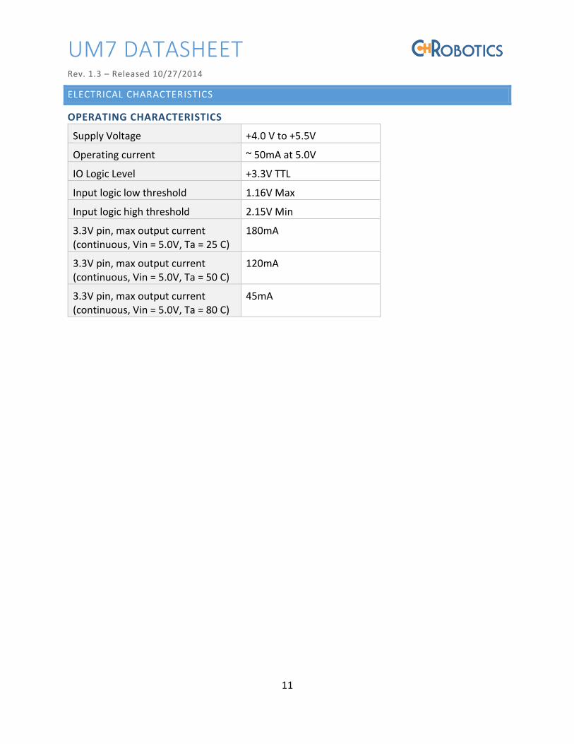
UM7 DATASHEET
Rev. 1.3 – Released 10/27/2014
11
ELECTRICAL CHARACTERISTICS
OPERATING CHARACTERISTICS
Supply Voltage +4.0 V to +5.5V
Operating current ~ 50mA at 5.0V
IO Logic Level +3.3V TTL
Input logic low threshold 1.16V Max
Input logic high threshold 2.15V Min
3.3V pin, max output current
(continuous, Vin = 5.0V, Ta = 25 C)
180mA
3.3V pin, max output current
(continuous, Vin = 5.0V, Ta = 50 C)
120mA
3.3V pin, max output current
(continuous, Vin = 5.0V, Ta = 80 C)
45mA

UM7 DATASHEET
Rev. 1.3 – Released 10/27/2014
12
PINOUT
MAIN IO HEADER
Mating connector: JST part number ZHR-5(P)
Pin Name Description
GND Supply ground
3.3V 3.3V output from onboard LDO. May also
function as a 3.3V supply input if Vin is left
unconnected.
Vin Supply voltage input. 5.0V nominal.
TX UART TX output (3.3V TTL)
RX UART RX input (3.3V TTL)
* The Main IO Header contains all pins required to operate the UM7 normally. The IO
Expansion and Programming headers are optional.
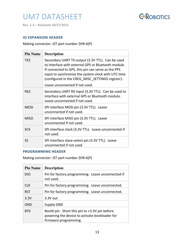
UM7 DATASHEET
Rev. 1.3 – Released 10/27/2014
13
IO EXPANSION HEADER
Mating connector: JST part number ZHR-6(P)
Pin Name Description
TX2 Secondary UART TX output (3.3V TTL). Can be used
to interface with external GPS or Bluetooth module.
If connected to GPS, this pin can serve as the PPS
input to synchronize the system clock with UTC time
(configured in the CREG_MISC_SETTINGS register).
Leave unconnected if not used.
RX2 Secondary UART RX input (3.3V TTL). Can be used to
interface with external GPS or Bluetooth module.
Leave unconnected if not used.
MOSI SPI interface MOSI pin (3.3V TTL). Leave
unconnected if not used.
MISO SPI interface MISO pin (3.3V TTL). Leave
unconnected if not used.
SCK SPI interface clock (3.3V TTL). Leave unconnected if
not used.
SS SPI interface slave-select pin (3.3V TTL). Leave
unconnected if not used.
PROGRAMMING HEADER
Mating connector: JST part number ZHR-6(P)
Pin Name Description
DIO Pin for factory programming. Leave unconnected if
not used.
CLK Pin for factory programming. Leave unconnected.
RST Pin for factory programming. Leave unconnected.
3.3V 3.3V out
GND Supply GND
BT0 Boot0 pin. Short this pin to +3.3V pin before
powering the device to activate bootloader for
firmware programming.

UM7 DATASHEET
Rev. 1.3 – Released 10/27/2014
14
MECHANICAL DRAWING
Dimensions are in inches. Unless otherwise noted, dimensional tolerances are within +/-
. .
TOP VIEW
SIDE VIEW

UM7 DATASHEET
Rev. 1.3 – Released 10/27/2014
15
SPI COMMUNICATION
The UM7 SPI bus operates at a +3.3V logic level. The UM7 is a slave on the bus, remaining
inactive unless queried by a master device. Since the SPI bus will not always be used, bus
inputs (MOSI, SCK, SS) are pulled to +3.3V internally. This prevents noise from being registered
by the UM7 as attempts to communicate with the sensor.
The UM7 SPI clock (SCK) is active high, with data clocked in on the first rising edge (usually
labeled SPI Mode 0 on microcontrollers and other devices). The master should place its data on
the MOSI line on the clock falling edge.
The maximum SPI clock rate is 10 MHz. However the UM7 needs at least 5 microseconds
between bytes to copy the next byte into the SPI transmit register. For high clock rates, this
means that a delay must be added between consecutive bytes for correct operation.
All SPI operations begin when the master writes two control bytes to the bus. The first byte
indicates whether the operation is a register read (0x00) or a write (0x01). The second byte is
the address of the register being accessed.
A read operation is performed by writing the control byte 0x00 to the MOSI line, followed by
the address of the register to be read. During the next four transfers, the UM7 will write the
contents of the register to the MISO line starting with the most-significant byte in the register
as shown in Figure 2 - Single Register Read Operation. The master should pull the MOSI line
low during the remainder of the read.
A read operation can be extended to read more than one register at a time as shown in Figure 3
- Multiple Register Read Operation to initiate the batch read, the master should write the
address of the next desired register to the MOSI line while last byte of the previous register is
being transmitted by the UM7.
A write operation is performed by writing the control byte 0x01 to the MOSI line, followed by
the address of the register to modify. During the next four transfers, the UM7 will read the
data from the MOSI line and write it to the specified register. During a write operation, the
UM7 will pull the MISO line low to indicate that it is receiving data. There is no batch write
operation. The structure of a write operation is illustrated in Figure 4 - Single Register Write
Operation.
Commands are initiated over the SPI bus by sending a write operation to the command
address, with all four data bytes at zero. The UM7 will not report that a command was executed
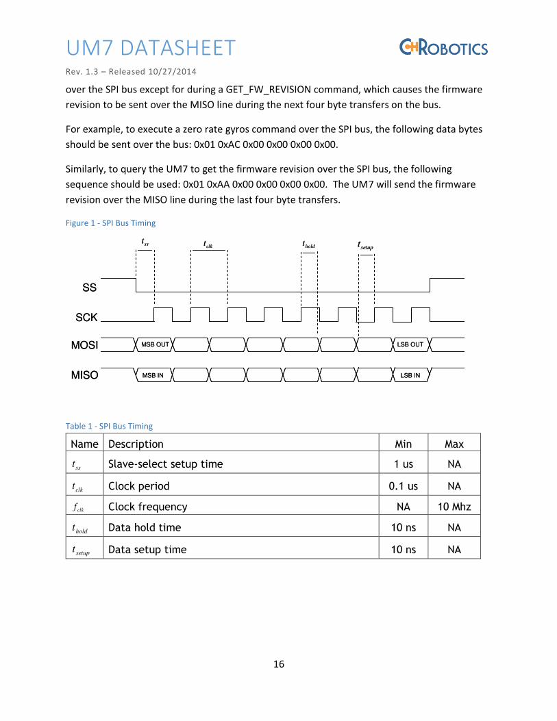
UM7 DATASHEET
Rev. 1.3 – Released 10/27/2014
16
over the SPI bus except for during a GET_FW_REVISION command, which causes the firmware
revision to be sent over the MISO line during the next four byte transfers on the bus.
For example, to execute a zero rate gyros command over the SPI bus, the following data bytes
should be sent over the bus: 0x01 0xAC 0x00 0x00 0x00 0x00.
Similarly, to query the UM7 to get the firmware revision over the SPI bus, the following
sequence should be used: 0x01 0xAA 0x00 0x00 0x00 0x00. The UM7 will send the firmware
revision over the MISO line during the last four byte transfers.
Figure 1 - SPI Bus Timing
Table 1 - SPI Bus Timing
Name Description Min Max
sst Slave-select setup time 1 us NA
clkt Clock period 0.1 us NA
clkf Clock frequency NA 10 Mhz
holdt Data hold time 10 ns NA
setupt Data setup time 10 ns NA
SCK
SS
MISO
MOSI MSB OUT
MSB IN LSB IN
LSB OUT
sstclkt holdt
setupt
SCK
SS
MISO
MOSI MSB OUT
MSB IN LSB IN
LSB OUT
sstclkt holdt
setupt
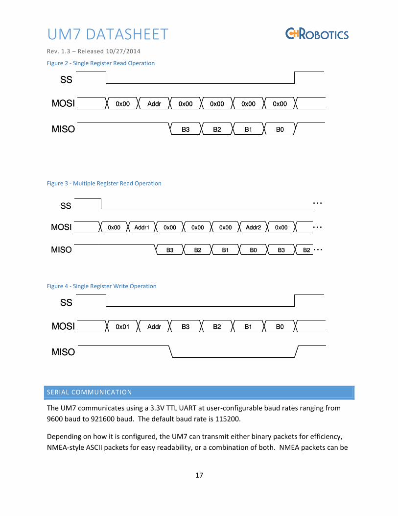
UM7 DATASHEET
Rev. 1.3 – Released 10/27/2014
17
Figure 2 - Single Register Read Operation
Figure 3 - Multiple Register Read Operation
Figure 4 - Single Register Write Operation
SERIAL COMMUNICATION
The UM7 communicates using a 3.3V TTL UART at user-configurable baud rates ranging from
9600 baud to 921600 baud. The default baud rate is 115200.
Depending on how it is configured, the UM7 can transmit either binary packets for efficiency,
NMEA-style ASCII packets for easy readability, or a combination of both. NMEA packets can be
SS
MISO
MOSI 0x00 Addr 0x00 0x00 0x00 0x00
B3 B2 B1 B0
SS
MISO
MOSI 0x00 Addr 0x00 0x00 0x00 0x00
B3 B2 B1 B0
SS
MISO
MOSI 0x00 Addr1 0x00 0x00 0x00 Addr2
B3 B2 B1 B0 B3 B2
0x00
…
…
…SS
MISO
MOSI 0x00 Addr1 0x00 0x00 0x00 Addr2
B3 B2 B1 B0 B3 B2
0x00
…
…
…
SS
MISO
MOSI 0x01 Addr B3 B2 B1 B0
SS
MISO
MOSI 0x01 Addr B3 B2 B1 B0

UM7 DATASHEET
Rev. 1.3 – Released 10/27/2014
18
transmitted by the UM7 at rates of up to 100 Hz. Binary packets can be transmitted at rates of
up to 255 Hz.
The communication architecture of the UM7 allows the user to select both what data is
transmitted, and at what rates. Each packet type can be configured to transmit at its own
unique rate. For example, the UM7 might be configured to transmit a health packet once a
second, a position packet 10 times per second, and attitude packets 250 times per second.
Alternatively, the user can poll the sensor to read any subset of its data registers at any time.
This flexible communication architecture allows the user to take full advantage of the limited
bandwidth available on the UART.
If the UM7 is configured to transmit more information than can fit on the serial bus, a
COM_OVERFLOW flag will be set i the de i e s health register.
To configure the UM7 s t a s issio setti gs a d othe setti gs, binary packets must be sent to
change the settings in a variety of configuration registers, described later in this document.
Settings can be changed manually by constructing and sending the appropriate packets, or
more easily by using the CHR Serial Interface software. Configuration settings can be saved to
device FLASH so that they persist when power is removed.
Packet transmission rates are configured using registers CREG_COM_RATES1 through
CREG_COM_RATES7 (See the Configuration Registers section for more details about
configuration registers).
The serial baud rate can be configured by writing to the CREG_COM_SETTINGS register.
For more details about the register architecture on the UM7, see the Register Overview section.
For specific details about how to write to and read from registers, see the Binary Packet
Structure se tio , o efe to the UM Use s Guide, a aila le at www.chrobotics.com, to learn
to use the CHR Serial Interface software.
NMEA PACKETS
NMEA packets provide data in human-readable, comma-separated messages over the serial
port. These packets are easily interpreted by human operators and, depending on the context,
by computers as well. The downside is that they are less efficient than binary packets, taking
more time to transmit the same amount of information.

UM7 DATASHEET
Rev. 1.3 – Released 10/27/2014
19
Each NMEA packet begins with a $ symbol and ends with a carriage- etu , li efeed pai \r\ , simply a new line when viewed on a serial terminal). Between the start and end symbols, the
packet consists of a predefined comma-separated list containing sensor data.
NMEA packets can be automatically sent by the UM7 at between 1 Hz and 100 Hz. The actual
amount of data that can be transmitted depends on the baud rate, and some NMEA packets
(like the sensor data packet, for example) can quickly overwhelm the serial bus, preventing the
data from being transmitted as often as requested.
While NMEA messages can be transmitted by the UM7, the UM7 can only be configured using
binary packets – the UM7 transmits NMEA packets, but there are no NMEA packets defined to
change configuration settings.
Each NMEA sentence transmitted by the UM7 begins with the text sequence $PCHRx. The
ha a te P i di ates that the pa ket to follo is a p op ieta pa ket i.e. it is t a sta da d NMEA pa ket . The se ue e CH‘ i dicates that it is a CH Robotics packet. Finally, the
ha a te a ies depe di g o the e a t pa ket ei g t a s itted.
Health Packet - $PCHRH
DESCRIPTION
The NMEA health packet contains a summary of health-related information, including basic GPS
information and sensor status information.
PACKET FORMAT
$PCHRH,time,sats_used,sats_in_view,HDOP,mode,COM,accel,gyro,mag,GPS,res,res,res,*checks
um
e.g. $PCHRH,105.015,05,11,1.5,0,0,0,0,0,0,0,0,0,*70
PACKET FIELD DESCRIPTION
Field Description
$PCHRH Header field, always precedes the health packet
time e.g. 105.015
This field can be up to 13 digits long. There will always be three decimal digits.
If no GPS is connected, this represents the amount of time in seconds since the
sensor was last turned on. If GPS with PPS is properly connected, this is
synchronized to UTC time of day.
sats_used e.g. 05
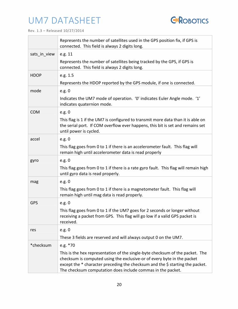
UM7 DATASHEET
Rev. 1.3 – Released 10/27/2014
20
Represents the number of satellites used in the GPS position fix, if GPS is
connected. This field is always 2 digits long.
sats_in_view e.g. 11
Represents the number of satellites being tracked by the GPS, if GPS is
connected. This field is always 2 digits long.
HDOP e.g. 1.5
Represents the HDOP reported by the GPS module, if one is connected.
mode e.g. 0
I di ates the UM ode of ope atio . i di ates Eule A gle ode. indicates quaternion mode.
COM e.g. 0
This flag is 1 if the UM7 is configured to transmit more data than it is able on
the serial port. If COM overflow ever happens, this bit is set and remains set
until power is cycled.
accel e.g. 0
This flag goes from 0 to 1 if there is an accelerometer fault. This flag will
remain high until accelerometer data is read properly
gyro e.g. 0
This flag goes from 0 to 1 if there is a rate gyro fault. This flag will remain high
until gyro data is read properly.
mag e.g. 0
This flag goes from 0 to 1 if there is a magnetometer fault. This flag will
remain high until mag data is read properly.
GPS e.g. 0
This flag goes from 0 to 1 if the UM7 goes for 2 seconds or longer without
receiving a packet from GPS. This flag will go low if a valid GPS packet is
received.
res e.g. 0
These 3 fields are reserved and will always output 0 on the UM7.
*checksum e.g. *70
This is the hex representation of the single-byte checksum of the packet. The
checksum is computed using the exclusive-or of every byte in the packet
except the * character preceding the checksum and the $ starting the packet.
The checksum computation does include commas in the packet.

UM7 DATASHEET
Rev. 1.3 – Released 10/27/2014
21
Pose packet - $PCHRP
DESCRIPTION
The NMEA pose packet contains sensor position and Euler Angle attitude. The position
i fo atio i this pa ket is gi e i ete s a a f o the se so s o figurable home lat/lon
and altitude (the GPS Pose packet provides position in terms of latitude/longitude instead).
PACKET FORMAT
$PCHRP,time,pn,pe,alt,roll,pitch,yaw,heading,*checksum
e.g. $PCHRP,105.015,-501.234,-501.234,15.521,20.32,20.32,20.32,20.32,*47
PACKET FIELD DESCRIPTION
Field Description
$PCHRP Header field, always precedes the pose packet
time e.g. 105.015
This field can be up to 13 digits long. There will always be 3 decimal digits.
If no GPS is connected, this represents the amount of time in seconds since the
sensor was last turned on. If GPS with PPS is properly connected, this is
synchronized to UTC time of day.
pn e.g. -501.234
This field can be up to 10 digits long. There will always be 3 decimal digits.
If GPS is o e ted, this ep ese ts the se so s positio i ete s o th of the configurable home position. If the sensor is more than 99 km away from
its home position, the fractional digits are truncated.
pe e.g. -501.234
This field can be up to 10 digits long. There will always be 3 decimal digits.
If GPS is connected, this rep ese ts the se so s positio i ete s east of the configurable home position. If the sensor is more than 99 km away from its
home position, the fractional digits are truncated.
alt e.g. 15.521
This field can be up to 10 digits long. There will always be 3 decimal digits.

UM7 DATASHEET
Rev. 1.3 – Released 10/27/2014
22
If GP“ is o e ted, this ep ese ts the se so s altitude i ete s f o the configurable home position. If the sensor is more than 99 km away from its
home position, the fractional digits are truncated.
roll e.g. 20.32
This field can be up to 7 digits long. There will always be 2 decimal digits.
This represents the roll angle of the sensor in degrees.
pitch e.g. 20.32
This field can be up to 7 digits long. There will always be 2 decimal digits.
This represents the pitch angle of the sensor in degrees.
yaw e.g. 20.32
This field can be up to 7 digits long. There will always be 2 decimal digits.
This represents the yaw angle of the sensor in degrees.
heading e.g. 20.32
This field can be up to 7 digits long. There will always be 2 decimal digits.
This represents the heading angle of the sensor in degrees, as reported by the
GPS module if connected.
*checksum e.g. *47
This is the hex representation of the single-byte checksum of the packet. The
checksum is computed using the exclusive-or of every byte in the packet
except the * character preceding the checksum and the $ starting the packet.
The checksum computation does include commas in the packet.
Attitude Packet - $PCHRA
DESCRIPTION
The NMEA attitude packet contains sensor Euler Angle attitude and GPS heading if GPS is
connected.
PACKET FORMAT
$PCHRA,time,roll,pitch,yaw,heading,*checksum
e.g. $PCHRA,105.015,20.32,20.32,20.32,20.32,*66
PACKET FIELD DESCRIPTION
Field Description
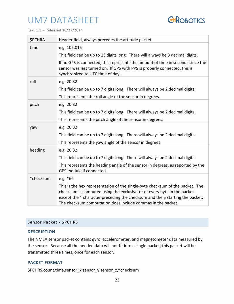
UM7 DATASHEET
Rev. 1.3 – Released 10/27/2014
23
$PCHRA Header field, always precedes the attitude packet
time e.g. 105.015
This field can be up to 13 digits long. There will always be 3 decimal digits.
If no GPS is connected, this represents the amount of time in seconds since the
sensor was last turned on. If GPS with PPS is properly connected, this is
synchronized to UTC time of day.
roll e.g. 20.32
This field can be up to 7 digits long. There will always be 2 decimal digits.
This represents the roll angle of the sensor in degrees.
pitch e.g. 20.32
This field can be up to 7 digits long. There will always be 2 decimal digits.
This represents the pitch angle of the sensor in degrees.
yaw e.g. 20.32
This field can be up to 7 digits long. There will always be 2 decimal digits.
This represents the yaw angle of the sensor in degrees.
heading e.g. 20.32
This field can be up to 7 digits long. There will always be 2 decimal digits.
This represents the heading angle of the sensor in degrees, as reported by the
GPS module if connected.
*checksum e.g. *66
This is the hex representation of the single-byte checksum of the packet. The
checksum is computed using the exclusive-or of every byte in the packet
except the * character preceding the checksum and the $ starting the packet.
The checksum computation does include commas in the packet.
Sensor Packet - $PCHRS
DESCRIPTION
The NMEA sensor packet contains gyro, accelerometer, and magnetometer data measured by
the sensor. Because all the needed data will not fit into a single packet, this packet will be
transmitted three times, once for each sensor.
PACKET FORMAT
$PCHRS,count,time,sensor_x,sensor_y,sensor_z,*checksum

UM7 DATASHEET
Rev. 1.3 – Released 10/27/2014
24
e.g. $PCHRS,1,105.015,-0.9987,-0.9987,-0.9987,*79
PACKET FIELD DESCRIPTION
Field Description
$PCHRS Header field, always precedes the attitude packet
count e.g. 1
This flag can be 0, 1, or 2. If 0, then the packet contains gyro data. If 1, then
the packet contains accelerometer data. If 3, then the packet contains
magnetometer data.
time e.g. 105.015
This field can be up to 13 digits long. There will always be 3 decimal digits.
If no GPS is connected, this represents the amount of time in seconds since the
sensor was last turned on. If GPS with PPS is properly connected, this is
synchronized to UTC time of day.
sensor_x e.g. -0.9987
This field can be up to 11 digits long. On accel and mag data, there will always
be 4 decimal digits. On gyro data, there will always be 2 decimal digits.
This represents se so data as spe ified i the ou t field a o e. Gyro data is
in degrees per second. Accelerometer data is in gravities. Magnetometer data
is unit-norm (unitless).
sensor_x e.g. -0.9987
This field can be up to 11 digits long. On accel and mag data, there will always
be 4 decimal digits. On gyro data, there will always be 2 decimal digits.
This ep ese ts se so data as spe ified i the ou t field a o e. G o data is in degrees per second. Accelerometer data is in gravities. Magnetometer data
is unit-norm (unitless).
sensor_x e.g. -0.9987
This field can be up to 11 digits long. On accel and mag data, there will always
be 4 decimal digits. On gyro data, there will always be 2 decimal digits.
This represents sensor data as specified in the ou t field a o e. G o data is in degrees per second. Accelerometer data is in gravities. Magnetometer data
is unit-norm (unitless).
*checksum e.g. *79
This is the hex representation of the single-byte checksum of the packet. The checksum is computed using the exclusive-or of every byte in the packet except
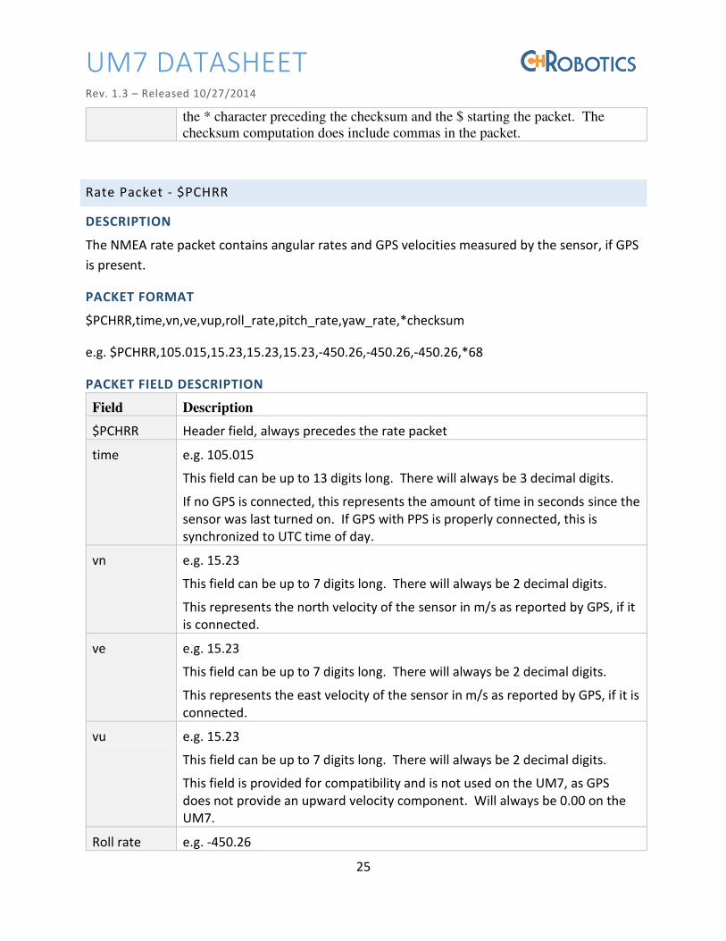
UM7 DATASHEET
Rev. 1.3 – Released 10/27/2014
25
the * character preceding the checksum and the $ starting the packet. The checksum computation does include commas in the packet.
Rate Packet - $PCHRR
DESCRIPTION
The NMEA rate packet contains angular rates and GPS velocities measured by the sensor, if GPS
is present.
PACKET FORMAT
$PCHRR,time,vn,ve,vup,roll_rate,pitch_rate,yaw_rate,*checksum
e.g. $PCHRR,105.015,15.23,15.23,15.23,-450.26,-450.26,-450.26,*68
PACKET FIELD DESCRIPTION
Field Description
$PCHRR Header field, always precedes the rate packet
time e.g. 105.015
This field can be up to 13 digits long. There will always be 3 decimal digits.
If no GPS is connected, this represents the amount of time in seconds since the
sensor was last turned on. If GPS with PPS is properly connected, this is
synchronized to UTC time of day.
vn e.g. 15.23
This field can be up to 7 digits long. There will always be 2 decimal digits.
This represents the north velocity of the sensor in m/s as reported by GPS, if it
is connected.
ve e.g. 15.23
This field can be up to 7 digits long. There will always be 2 decimal digits.
This represents the east velocity of the sensor in m/s as reported by GPS, if it is
connected.
vu e.g. 15.23
This field can be up to 7 digits long. There will always be 2 decimal digits.
This field is provided for compatibility and is not used on the UM7, as GPS
does not provide an upward velocity component. Will always be 0.00 on the
UM7.
Roll rate e.g. -450.26

UM7 DATASHEET
Rev. 1.3 – Released 10/27/2014
26
This field can be up to 8 digits long. There will always be 2 decimal digits.
This field p o ides the se so s easu ed oll ate i deg ees pe se o d.
Pitch rate e.g. -450.26
This field can be up to 8 digits long. There will always be 2 decimal digits.
This field p o ides the se so s easu ed pit h ate i deg ees pe se o d.
Yaw rate e.g. -450.26
This field can be up to 8 digits long. There will always be 2 decimal digits.
This field p o ides the se so s easu ed a ate i deg ees pe second.
*checksum e.g. *68
This is the hex representation of the single-byte checksum of the packet. The checksum is computed using the exclusive-or of every byte in the packet except the * character preceding the checksum and the $ starting the packet. The checksum computation does include commas in the packet.
GPS Pose Packet - $PCHRG
DESCRIPTION
The NMEA GPS pose packet contains GPS latitude, longitude, and altitude in addition to Euler
Angle attitude and GPS heading.
PACKET FORMAT
$PCHRG,time,latitude,longitude,altitude,roll,pitch,yaw,heading,*checksum
e.g. $PCHRG,105.015,40.047706,-111.742072,15.230,20.32,20.32,20.32,20.32,*49
PACKET FIELD DESCRIPTION
Field Description
$PCHRG Header field, always precedes the rate packet
time e.g. 105.015
This field can be up to 13 digits long. There will always be 3 decimal digits.
If no GPS is connected, this represents the amount of time in seconds since the
sensor was last turned on. If GPS with PPS is properly connected, this is
synchronized to UTC time of day.
latitude e.g. 40.047706
This field can be up to 11 digits long. There will always be 6 decimal digits.

UM7 DATASHEET
Rev. 1.3 – Released 10/27/2014
27
This represents the latitude as reported by GPS, in degrees.
longitude e.g. -111.742072
This field can be up to 11 digits long. There will always be 6 decimal digits.
This represents the longitude as reported by GPS, in degrees.
altitude e.g. 15.230
This field can be up to 11 digits long. There will always be 3 decimal digits.
This represents the altitude as reported by GPS
roll e.g. 20.32
This field can be up to 7 digits long. There will always be 2 decimal digits.
This represents the roll angle of the sensor in degrees.
pitch e.g. 20.32
This field can be up to 7 digits long. There will always be 2 decimal digits.
This represents the pitch angle of the sensor in degrees.
yaw e.g. 20.32
This field can be up to 7 digits long. There will always be 2 decimal digits.
This represents the yaw angle of the sensor in degrees.
heading e.g. 20.32
This field can be up to 7 digits long. There will always be 2 decimal digits.
This represents the heading angle of the sensor in degrees, as reported by the
GPS module if connected.
*checksum e.g. *49
This is the hex representation of the single-byte checksum of the packet. The checksum is computed using the exclusive-or of every byte in the packet except the * character preceding the checksum and the $ starting the packet. The checksum computation does include commas in the packet.
Quaternion Packet - $PCHRQ
DESCRIPTION
The NMEA quaternion packet contains the attitude quaternion (valid when the sensor is in
quaternion mode).
PACKET FORMAT

UM7 DATASHEET
Rev. 1.3 – Released 10/27/2014
28
$PCHRG,time,a,b,c,d,*checksum
e.g. $PCHRG,105.015,0.76592,0.76592,0.76592,0.76592,*60
PACKET FIELD DESCRIPTION
Field Description
$PCHRQ Header field, always precedes the quaternion packet
time e.g. 105.015
This field can be up to 13 digits long. There will always be 3 decimal digits.
If no GPS is connected, this represents the amount of time in seconds since the
sensor was last turned on. If GPS with PPS is properly connected, this is
synchronized to UTC time of day.
a e.g. 0.76592
This field can be up to 8 digits long. There will always be 5 decimal digits.
This represents element a of the attitude quaternion.
b e.g. 0.76592
This field can be up to 8 digits long. There will always be 5 decimal digits.
This represents element b of the attitude quaternion.
c e.g. 0.76592
This field can be up to 8 digits long. There will always be 5 decimal digits.
This represents element c of the attitude quaternion.
d e.g. 0.76592
This field can be up to 8 digits long. There will always be 5 decimal digits.
This represents element d of the attitude quaternion.
*checksum e.g. *60
This is the hex representation of the single-byte checksum of the packet. The checksum is computed using the exclusive-or of every byte in the packet except the * character preceding the checksum and the $ starting the packet. The checksum computation does include commas in the packet.

UM7 DATASHEET
Rev. 1.3 – Released 10/27/2014
29
BINARY PACKET STRUCTURE
Data transmitted and received by the UM7 is formatted into packets containing:
1. The three character start sequence 's', 'n', 'p' to indicate the start of a new packet (i.e.
start new packet)
2. A "packet type" (PT) byte describing the function and length of the packet
3. An address byte indicating the address of the register or command
4. A sequence of data bytes, the length of which is specified in the PT byte
5. A two-byte checksum for error-detection
Table 2 - UART Serial Packet Structure
's' 'n' 'p' packet type
(PT)
Address Data Bytes (D0...DN-
1)
Checksum 1 Checksum 0
All binary packets sent and received by the UM7 must conform to the format given above.
The PT byte specifies whether the packet is a read or a write operation, whether it is a batch
operation, and the length of the batch operation (when applicable). The PT byte is also used by
the UM7 to respond to commands. The specific meaning of each bit in the PT byte is given
below.
Table 3 - Packet Type (PT) byte
7 6 5 4 3 2 1 0
Has Data Is Batch BL3 BL2 BL1 BL0 Hidden CF
Table 4 - Packet Type (PT) Bit Descriptions
Bit(s) Description
7 Has Data: If the packet contains data, this bit is set (1). If not, this bit is cleared (0).
6 Is Batch: If the packet is a batch operation, this bit is set (1). If not, this bit is
cleared (0)
5:2 Batch Length (BL): Four bits specifying the length of the batch operation. Unused
if bit 7 is cleared. The maximum batch length is therefore 2^4 = 16
1 Hidde : If set, the the pa ket add ess spe ified i the Add ess field is a hidde add ess. Hidde egiste s a e used to sto e fa to ali atio a d filte

UM7 DATASHEET
Rev. 1.3 – Released 10/27/2014
30
tuning coefficients that do not typically need to be viewed or modified by the user.
This bit should always be set to 0 to avoid altering factory configuration.
0 Command Failed (CF): Used by the autopilot to report when a command has failed.
Must be set to zero for all packets written to the UM7.
The address byte specifies which register will be involved in the operation. During a read
operation (Has Data = 0), the address specifies which register to read. During a write operation
(Has Data = 1), the address specifies where to place the data contained in the data section of
the packet. For a batch read/write operation, the address byte specifies the starting address of
the operation.
The "Data Bytes" section of the packet contains data to be written to one or more registers.
There is no byte in the packet that explicitly states how many bytes are in this section because
it is possible to determine the number of data bytes that should be in the packet by evaluating
the PT byte.
If the Has Data bit in the PT byte is cleared (Has Data = 0), then there are no data bytes in the
packet and the Checksum immediately follows the address. If, on the other hand, the Has Data
bit is set (Has Data = 1) then the number of bytes in the data section depends on the value of
the Is Batch and Batch Length portions of the PT byte.
For a batch operation (Is Batch = 1), the length of the packet data section is equal to 4*(Batch
Length). Note that the batch length refers to the number of registers in the batch, NOT the
number of bytes. Registers are 4 bytes long.
For a non-batch operation (Is Batch = 0), the length of the data section is equal to 4 bytes (one
register). The data section lengths and total packet lengths for different PT configurations are
shown below.
Table 5 - Packet Length Summary
Has
Data
Is Batch Data Section Length
(bytes)
Total Packet Length (bytes)
0 NA 0 7
1 0 4 11
1 1 4*(Batch Length) 7 + 4*(Batch Length)
Note that if a packet is a batch operation, the batch length must be greater than zero.

UM7 DATASHEET
Rev. 1.3 – Released 10/27/2014
31
The two checksum bytes consist of the unsigned 16-bit sum of all preceding bytes in the packet,
including the packet header.
Read Operations
To initiate a serial read of one or more registers aboard the sensor, a packet should be sent to
the UM7 with the "Has Data" bit cleared. This tells the device that this will be a read operation
from the address specified in the packet's "Address" byte. If the "Is Batch" bit is set, then the
packet will trigger a batch read in which the "Address" byte specifies the address of the first
register to be read.
In response to a read packet, the UM7 will send a packet in which the "Has Data" bit is set, and
the "Is Batch" and "Batch Length" bits are equivalent to those of the packet that triggered the
read operation. The register data will be contained in the "Data Bytes" section of the packet.
Write Operations
To initiate a serial write into one or more registers aboard the sensor, a packet should be sent
to the UM7 with the "Has Data" bit set. This tells the device that the incoming packet contains
data that should be written to the register specified by the packet's "Address" byte. If a batch
write operation is to be performed, the "Is Batch" bit should be set, and the "Batch Length" bits
should indicate the number of registers that are to be written to.
In response to a write packet, the UM7 will update the contents of the specified register(s) with
the contents of the data section of the packet. It will then transmit a COMMAND_COMPLETE
packet to indicate that the write operation succeeded. A COMMAND_COMPLETE packet is a
packet with PT = 0 (no data, no batch) and with an address matching the address of the register
to which the write operation was made, or the start address of the write operation if this was a
batch write.
Note that the COMMAND_COMPLETE packet is equivalent to a packet that would cause the
autopilot to initiate a read operation on the address to which data was just written. Since the
packet is going from the sensor to the host, however, its meaning is different (it would not
make sense for the autopilot to request the contents of one of its registers from an external
host).
Command Operations
There are a variety of register address that do not correspond with actual physical registers
aboard the UM7. These "command" addresses are used to cause the sensor to execute specific

UM7 DATASHEET
Rev. 1.3 – Released 10/27/2014
32
commands (there are commands for executing calibration operations, resetting the onboard
filters, etc. See the Register Overview in this document for more details).
To initiate a command, simply send a packet to the autopilot with the command's address in
the packet "Address" byte. The PT byte should be set to zero for a command operation.
If the UM7 successfully completes the specified command, then a COMMAND_COMPLETE
packet is returned with the command address in the "Address" byte of the response packet. If
the command fails, the device responds by sending a COMMAND_FAILED packet. The
COMMAND_FAILED packet is equivalent to the COMMAND_COMPLETE packet except that the
"Command Failed" bit in the PT byte is set (CF = 1).
In some cases, a command will cause specific packets to be sent other than the
COMMAND_COMPLETE packet. A GET_FW_VERSION command will, for example, return a
packet containing the version of the firmware installed on the UM7. In this and similar cases,
the COMMAND_COMPLETE packet is not sent.
Example Binary Communication Code
RECEIVING DATA FROM THE UM7
There are a lot of ways to parse the incoming data from the UM7. Often, it is easiest to write a
generalized parser that takes all incoming data and extracts the data, address, and packet type
information and then makes it easily accessible to the user program. The following code shows
an example of a good general parser that can be used to extract packet data.
// Structure for holding received packet information
typedef struct UM7_packet_struct
uint8_t Address;
uint8_t PT;
uint16_t Checksum;
uint8_t data_length;
uint8_t data[30];
UM7_packet;

UM7 DATASHEET
Rev. 1.3 – Released 10/27/2014
33
// parse_serial_data
// This fu tio pa ses the data i _data ith le gth _le gth a d atte pts to fi d a pa ket
// i the data. If a pa ket is fou d, the st u tu e pa ket is filled ith the pa ket data.
// If there is not enough data for a full packet in the provided array, parse_serial_data returns 1.
// If there is enough data, but no packet header was found, parse_serial_data returns 2.
// If a packet header was found, but there was insufficient data to parse the whole packet,
// then parse_serial_data returns 3. This could happen if not all of the serial data has been
// received when parse_serial_data is called.
// If a packet was received, but the checksum was bad, parse_serial_data returns 4.
// If a good packet was received, parse_serial_data fills the UM7_packet structure and returns 0.
uint8_t parse_serial_data( uint8_t* rx_data, uint8_t rx_length, UM7_packet* packet )
uint8_t index;
// Make sure that the data buffer provided is long enough to contain a full packet
// The minimum packet length is 7 bytes
if( rx_length < 7 )
return 1;
// T to fi d the s p sta t se ue e fo the pa ket
for( index = 0; index < (rx_length – 2); index++ )
// Che k fo s p . If fou d, i ediatel e it the loop
if _data[i de ] == s && _data[i de + ] == && _data[i de + ] == p
break;
uint8_t packet_index = index;
// Check to see if the variable pa ket_i de is e ual to _le gth - 2). If it is, then the above
// loop executed to completion and never found a packet header.
UM7 DATASHEET
Rev. 1.3 – Released 10/27/2014
34
if( packet_index == (rx_length – 2) )
return 2;
// If we get here, a packet header was found. Now check to see if we have enough room
// left i the uffe to o tai a full pa ket. Note that at this poi t, the a ia le pa ket_i de
// o tai s the lo atio of the s ha a te i the uffe the fi st te i the header)
if( (rx_length – packet_index) < 7 )
return 3;
// We e fou d a pa ket heade , a d the e is e ough spa e left i the uffe fo at least
// the smallest allowable packet length (7 bytes). Pull out the packet type byte to determine
// the actual length of this packet
uint8_t PT = rx_data[packet_index + 3];
// Do some bit-level manipulation to determine if the packet contains data and if it is a batch
// We have to do this because the individual bits in the PT byte specify the contents of the
// packet.
uint8_t packet_has_data = (PT >> 7) & 0x01; // Check bit 7 (HAS_DATA)
uint8_t packet_is_batch = (PT >> 6) & 0x01; // Check bit 6 (IS_BATCH)
uint8_t batch_length = (PT >> 2) & 0x0F; // Extract the batch length (bits 2 through 5)
// Now finally figure out the actual packet length
uint8_t data_length = 0;
if( packet_has_data )
if( packet_is_batch )
// Pa ket has data a d is a at h. This ea s it o tai s at h_le gth' egiste s, ea h
// of which has a length of 4 bytes
data_length = 4*batch_length;
else // Packet has data but is not a batch. This means it contains one register (4 bytes)
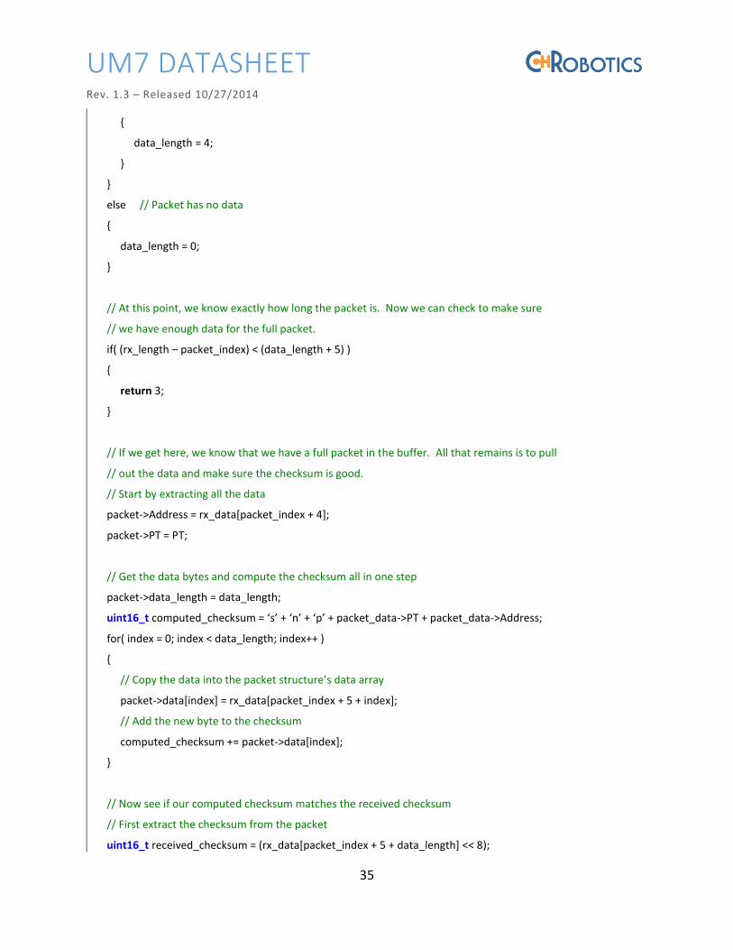
UM7 DATASHEET
Rev. 1.3 – Released 10/27/2014
35
data_length = 4;
else // Packet has no data
data_length = 0;
// At this point, we know exactly how long the packet is. Now we can check to make sure
// we have enough data for the full packet.
if( (rx_length – packet_index) < (data_length + 5) )
return 3;
// If we get here, we know that we have a full packet in the buffer. All that remains is to pull
// out the data and make sure the checksum is good.
// Start by extracting all the data
packet->Address = rx_data[packet_index + 4];
packet->PT = PT;
// Get the data bytes and compute the checksum all in one step
packet->data_length = data_length;
uint16_t o puted_ he ksu = s + + p + pa ket_data->PT + packet_data->Address;
for( index = 0; index < data_length; index++ )
// Cop the data i to the pa ket st u tu e s data a a
packet->data[index] = rx_data[packet_index + 5 + index];
// Add the new byte to the checksum
computed_checksum += packet->data[index];
// Now see if our computed checksum matches the received checksum
// First extract the checksum from the packet
uint16_t received_checksum = (rx_data[packet_index + 5 + data_length] << 8);

UM7 DATASHEET
Rev. 1.3 – Released 10/27/2014
36
received_checksum |= rx_data[packet_index + 6 + data_length];
// No he k to see if the do t at h
if( received_checksum != computed_checksum )
return 4;
// At this poi t, e e e ei ed a full pa ket ith a good he ksu . It is al ead
// fully parsed and copied to the pa ket st u tu e, so etu to i di ate that a pa ket as
// processed.
return 0;
Once the packet has been parsed and copied into the packet structure, accessing the desired
data is as simple as watching for packets with the desired address, checking the data length to
ake su e it is as lo g as ou e pe t, a d the pulli g the data out of the pa ket s data a a .
GETTING THE FIRMWARE REVISION
To read the firmware revision from the UM7, a GET_FW_REVISION command should be sent to
the over the serial port. Recall that to initiate a command on the UM7, a read packet should be
sent usi g the o a d s add ess i the Add ess te of the pa ket. Fo a GET_FW_‘EVI“ION command, the address is 170 (0xAA).
C-code for constructing and sending the command is shown below:
uint8_t tx_data[20];
t _data[ ] = s ;
t _data[ ] = ;
t _data[ ] = p ;
tx_data[3] = 0x00; // Packet Type byte
tx_data[4] = 0xAA; // Address of GET_FW_REVISION register
tx_data[5] = 0x01; // Checksum high byte
tx_data[6] = 0xFB; // Checksum low byte
USART_transmit( tx_data, 7 );

UM7 DATASHEET
Rev. 1.3 – Released 10/27/2014
37
The preceding code assumes that a function called USART_transmit( uint8_t* data, uint8_t
le gth e ists that t a s its le gth ha a te s f o the p o ided uffe o e the UART.
Once the UM7 receives the above packet, it will respond with a packet containing the firmware
revision. Example code for receiving the firmware revision packet is given below. Note that
this code assumes that the serial data is being received and transferred to a buffer before the
example code is executed.
UM7_packet new_packet;
char FW_revision[5];
// Call the parse_serial_data function to handle the incoming serial data. The serial data should
// e pla ed i _data a d the le gth i rx_data_length efo e this fu tio is alled.
if( !parse_serial_data( rx_data, rx_data_length, &new_packet )
// We got a good packet! Check to see if it is the firmware revision
if( packet.Address == 0xAA )
// Extract the firmware revision
FW_revision[0] = packet.data[0];
FW_revision[1] = packet.data[1];
FW_revision[2] = packet.data[2];
FW_revision[3] = packet.data[3];
FW_ e isio [4] = \ ; // Null-terminate the FW revision so we can use it like a string
// P i t the fi a e e isio to the te i al o do hate e else ou a t…
p i tf Got the fi a e e isio : %s\r\ , FW_ e isio ;
// TODO: Check to see if any of the other packets that we care about have been found.
// If so, do stuff with them.
Note that it is not always sufficient to simply check the address of the data register that you
want to read. In almost all cases, data automatically transmitted by the UM7 is sent in batch
operations to improve efficiency. For example, when processed rate gyro is transmitted, it is
sent in one batch packet containing registers 97 (gyro x), 98 (gyro y), 99 (gyro z), and 100 (gyro
time). Thus, the address of the packet is 97, but it is a batch packet with batch length 4.

UM7 DATASHEET
Rev. 1.3 – Released 10/27/2014
38
REGISTER OVERVIEW
There are three types of registers onboard the UM7: configuration registers, data registers, and
command registers.
Configuration registers begin at address 0x00 and are used to configure UM7 s filter settings
and communication behavior. Configuration register contents can be written to onboard flash
to allow settings to be maintained when the device is powered down.
Data registers begin at address 0x55 (85), and store raw and processed data from the sensors
along with estimated states. Unlike configuration registers, data register contents cannot be
written to flash.
Command registers technically aren't registers at all, but they provide a convenient way to send
commands to the UM7 when those commands do not require additional data beyond the
command itself. For example, a command to run an onboard gyro bias calibration routine is
triggered by querying the ZERO_GYROS command register. By using a unique register address
for each command, the same communication architecture used to read from and write to data
and configuration registers can be used to send commands to the autopilot. Command
registers begin at address 0xAA.
Configuration Registers
Address Register Name Register Description
0x00 (0) CREG_COM_SETTINGS General communication settings
0x01 (1) CREG_COM_RATES1 Broadcast rate settings
0x02 (2) CREG_COM_RATES2 Broadcast rate settings
0x03 (3) CREG_COM_RATES3 Broadcast rate settings
0x04 (4) CREG_COM_RATES4 Broadcast rate settings
0x05 (5) CREG_COM_RATES5 Broadcast rate settings
0x06 (6) CREG_COM_RATES6 Broadcast rate settings
0x07 (7) CREG_COM_RATES7 Broadcast rate settings
0x08 (8) CREG_MISC_SETTINGS Misc. settings
0x09 (9) CREG_HOME_NORTH GPS north position to consider position 0
0x0A (10) CREG_HOME_EAST GPS east position to consider position 0
0x0B (11) CREG_HOME_UP GPS altitude to consider position 0
0x0C (12) CREG_GYRO_TRIM_X Bias trim for x-axis rate gyro

UM7 DATASHEET
Rev. 1.3 – Released 10/27/2014
39
0x0D (13) CREG_GYRO_TRIM_Y Bias trim for y-axis rate gyro
0x0E (14) CREG_GYRO_TRIM_Z Bias trim for z-axis rate gyro
0x0F (15) CREG_MAG_CAL1_1 Row 1, Column 1 of magnetometer calibration
matrix
0x10 (16) CREG_MAG_CAL1_2 Row 1, Column 2 of magnetometer calibration
matrix
0x11 (17) CREG_MAG_CAL1_3 Row 1, Column 3 of magnetometer calibration
matrix
0x12 (18) CREG_MAG_CAL2_1 Row 2, Column 1 of magnetometer calibration
matrix
0x13 (19) CREG_MAG_CAL2_2 Row 2, Column 2 of magnetometer calibration
matrix
0x14 (20) CREG_MAG_CAL2_3 Row 2, Column 3 of magnetometer calibration
matrix
0x15 (21) CREG_MAG_CAL3_1 Row 3, Column 1 of magnetometer calibration
matrix
0x16 (22) CREG_MAG_CAL3_2 Row 3, Column 2 of magnetometer calibration
matrix
0x17 (23) CREG_MAG_CAL3_3 Row 3, Column 3 of magnetometer calibration
matrix
0x18 (24) CREG_MAG_BIAS_X Magnetometer X-axis bias
0x19 (25) CREG_MAG_BIAS_Y Magnetometer Y-axis bias
0x1A (26) CREG_MAG_BIAS_Z Magnetometer Z-axis bias

UM7 DATASHEET
Rev. 1.3 – Released 10/27/2014
40
Data Registers
Address Register Name Register Description
0x55 (85) DREG_HEALTH Contains information about the health and
status of the UM7
0x56 (86) DREG_GYRO_RAW_XY Raw X and Y rate gyro data
0x57 (87) DREG_GYRO_RAW_Z Raw Z rate gyro data
0x58 (88) DREG_GYRO_TIME Time at which rate gyro data was acquired
0x59 (89) DREG_ACCEL_RAW_XY Raw X and Y accelerometer data
0x5A (90) DREG_ACCEL_RAW_Z Raw Z accelerometer data
0x5B (91) DREG_ACCEL_TIME Time at which accelerometer data was
acquired
0x5C (92) DREG_MAG_RAW_XY Raw X and Y magnetometer data
0x5D (93) DREG_MAG_RAW_Z Raw Z magnetometer data
0x5E (94) DREG_MAG_RAW_TIME Time at which magnetometer data was
acquired
0x5F (95) DREG_TEMPERATURE Temperature data
0x60 (96) DREG_TEMPERATURE_TIME Time at which temperature data was
acquired
0x61 (97) DREG_GYRO_PROC_X Processed x-axis rate gyro data
0x62 (98) DREG_GYRO_PROC_Y Processed y-axis rate gyro data
0x63 (99) DREG_GYRO_PROC_Z Processed z-axis rate gyro data
0x64 (100) DREG_GYRO_PROC_TIME Time at which rate gyro data was acquired
0x65 (101) DREG_ACCEL_PROC_X Processed x-axis accel data
0x66 (102) DREG_ACCEL_PROC_Y Processed y-axis accel data
0x67 (103) DREG_ACCEL_PROC_Z Processed z-axis accel data
0x68 (104) DREG_ACCEL_PROC_TIME Time at which accelerometer data was
acquired
0x69 (105) DREG_MAG_PROC_X Processed x-axis magnetometer data
0x6A (106) DREG_MAG_PROC_Y Processed y-axis magnetometer data
0x6B (107) DREG_MAG_PROC_Z Processed z-axis magnetometer data
0x6C (108) DREG_MAG_PROC_TIME Time at which magnetometer data was
acquired
UM7 DATASHEET
Rev. 1.3 – Released 10/27/2014
41
0x6D (109) DREG_QUAT_AB Quaternion elements A and B
0x6E (110) DREG_QUAT_CD Quaternion elements C and D
0x6F (111) DREG_QUAT_TIME Time at which the sensor was at the
specified quaternion rotation
0x70 (112) DREG_EULER_PHI_THETA Roll and pitch angles
0x71 (113) DREG_EULER_PSI Yaw angle
0x72 (114) DREG_EULER_PHI_THETA_DOT Roll and pitch angle rates
0x73 (115) DREG_EULER_PSI_DOT Yaw rate
0x74 (116) DREG_EULER_TIME Time of computed Euler attitude and rates
0x75 (117) DREG_POSITION_NORTH North position in meters
0x76 (118) DREG_POSITION_EAST East position in meters
0x77 (119) DREG_POSITION_UP Altitude in meters
0x78 (120) DREG_POSITION_TIME Time of estimated position
0x79 (121) DREG_VELOCITY_NORTH North velocity
0x7A (122) DREG_VELOCITY_EAST East velocity
0x7B (123) DREG_VELOCITY_UP Altitude velocity
0x7C (124) DREG_VELOCITY_TIME Time of velocity estimate
0x7D (125) DREG_GPS_LATITUDE GPS latitude
0x7E (126) DREG_GPS_LONGITUDE GPS longitude
0x7F (127) DREG_GPS_ALTITUDE GPS altitude
0x80 (128) DREG_GPS_COURSE GPS course
0x81 (129) DREG_GPS_SPEED GPS speed
0x82 (130) DREG_GPS_TIME GPS time (UTC time of day in seconds)
0x83 (131) DREG_GPS_SAT_1_2 GPS satellite information
0x84 (132) DREG_GPS_SAT_3_4 GPS satellite information
0x85 (133) DREG_GPS_SAT_5_6 GPS satellite information
0x86 (134) DREG_GPS_SAT_7_8 GPS satellite information
0x87 (135) DREG_GPS_SAT_9_10 GPS satellite information
0x88 (136) DREG_GPS_SAT_11_12 GPS satellite information

UM7 DATASHEET
Rev. 1.3 – Released 10/27/2014
42
Commands
Address Name Description
0xAA (170) GET_FW_REVISION Causes the autopilot to respond with a
packet containing the current firmware
revision.
0xAB (171) FLASH_COMMIT Writes all current configuration settings
to flash
0xAC (172) RESET_TO_FACTORY Reset all settings to factory defaults
0xAD (173) ZERO_GYROS Causes the rate gyro biases to be
calibrated.
0xAE (174) SET_HOME_POSITION Sets the current GPS location as position
(0,0)
0xAF (175) RESERVED RESERVED
0xB0 (176) SET_MAG_REFERENCE Sets the magnetometer reference vector
0xB1 (177) RESERVED RESERVED
0xB2 (178) RESERVED RESERVED
0xB3 (179) RESET_EKF Resets the EKF
UM7 DATASHEET
Rev. 1.3 – Released 10/27/2014
43
CONFIGURATION REGISTERS
A set of 32-bit configuration registers allows the UM7 s behavior to be customized for specific
applications. In general, settings are most easily configured using the CHR Serial Interface,
which allows the contents of each configuration register to be set without understanding the
register contents at the bit/byte level.
This section outlines in detail the contents and functionality of each register.
CREG_COM_SETTINGS – 0x00 (0)
SUMMARY
The C‘EG_COM_“ETTING“ egiste is used to set the autopilot s se ial po t aud ate a d to enable or disable the automatic transmission of sensor data and estimated states (telemetry).
REGISTER CONTENTS
B3 B2
31 30 29 28 27 26 25 24 23 22 21 20 19 18 17 16
BAUD_RATE GPS_BAUD Reserved
B1 B0
15 14 13 12 11 10 9 8 7 6 5 4 3 2 1 0
Reserved GPS Reserved SAT Reserved
DESCRIPTION
Bits Name Description
31:28 BAUD_RATE Sets the baud rate of the UM7 main serial port.
0 = 9600
1 = 14400
2 = 19200
3 = 38400

UM7 DATASHEET
Rev. 1.3 – Released 10/27/2014
44
4 = 57600
5 = 115200
6 = 128000*
7 = 153600*
8 = 230400*
9 = 256000*
10 = 460800*
11 = 921600*
12:15 = reserved
* Most PC serial ports do not support baud-rates above 115200
27:24 GPS_BAUD Sets the baud rate of the UM7 auxiliary serial port.
0 = 9600
1 = 14400
2 = 19200
3 = 38400
4 = 57600
5 = 115200
23:9 Reserved These bits are reserved for future use
8 GPS If set, this bit causes GPS data to be transmitted automatically
whenever new GPS data is received. GPS data is stored in
registers 125 to 130. These registers will be transmitted in a batch
packet of length 6 starting at address 125.
7:5 Reserved These bits are reserved for future use
4 SAT If set, this bit causes satellite details to be transmitted whenever
they are provided by the GPS. Satellite information is stored in
registers 131 to 136. These registers will be transmitted in a batch
packet of length 6 beginning at address 131.
3:0 Reserved These bits are reserved for future use

UM7 DATASHEET
Rev. 1.3 – Released 10/27/2014
45
CREG_COM_RATES1 – 0x01 (1)
SUMMARY
The CREG_COM_RATES1 register sets desired telemetry transmission rates in Hz for raw
accelerometer, gyro, and magnetometer data. If the specified rate is 0, then no data is
transmitted.
REGISTER CONTENTS
B3 B2 B1 B0
RAW_ACCEL_RATE RAW_GYRO_RATE RAW_MAG_RATE Reserved
DESCRIPTION
Bits Name Description
31:24 RAW_ACCEL_RATE Specifies the desired raw accelerometer data broadcast rate
in Hz. The data is stored as an unsigned 8-bit integer,
yielding a maximum rate of 255 Hz.
23:16 RAW_GYRO_RATE Specifies the desired raw gyro data broadcast rate in Hz.
The data is stored as an unsigned 8-bit integer, yielding a
maximum rate of 255 Hz.
15:8 RAW_MAG_RATE Specifies the desired raw magnetometer data broadcast
rate in Hz. The data is stored as an unsigned 8-bit integer,
yielding a maximum rate of 255 Hz.
7:0 Reserved These bits are reserved.
Raw accelerometer data is stored in registers 89 to 91. When the raw accel rate is greater than 0,
the accelerometer data is transmitted in a batch packet of length 3 with start address 89.
Raw rate gyro data is stored in registers 86 to 88. When the raw gyro rate is greater than 0, the
rate gyro data is transmitted in a batch packet of length 3 with start address 86.
Raw magnetometer data is stored in registers 92 to 94. When the raw magnetometer rate is
greater than 0, the magnetometer data is transmitted in a batch packet of length 3 with start
address 92.
If the “all raw data rate” in CREG_COM_RATES2 is greater than 0, then all gyro, accelerometer, magnetometer, and pressure data will be transmitted together. The rates in
CREG_COM_RATES1 are then not used.
UM7 DATASHEET
Rev. 1.3 – Released 10/27/2014
46
CREG_COM_RATES2 – 0x02 (2)
SUMMARY
The CREG_COM_RATES2 register sets desired telemetry transmission rates for all raw data
and temperature. If the specified rate is 0, then no data is transmitted.
REGISTER CONTENTS
B3 B2 B1 B0
TEMP_RATE RES RES ALL_RAW_RATE
DESCRIPTION
Bits Name Description
31:24 TEMP_RATE Specifies the desired broadcast rate for temperature data.
The data is stored as an unsigned 8-bit integer, yielding a
maximum rate of 255 Hz.
23:16 RES These bits are reserved for future use
15:8 RES These bits are reserved for future use
7:0 ALL_RAW_RATE Specifies the desired broadcast rate for all raw sensor data.
If set, this overrides the broadcast rate setting for individual
raw data broadcast rates. The data is stored as an unsigned
8-bit integer, yielding a maximum rate of 255 Hz.
Temperature data is stored in registers 95 and 96. If the temperature broadcast rate is greater
than 0, then temperature data will be sent in a batch packet of length 2 with start address 95.
If all raw data is being transmitted (as specified by byte 3 of this register), then the temperature
data ill e t a s itted as pa t of the a at h pa ket at all a ate i stead of the a temperature rate.
Raw sensor/temperature data occupies registers 86 through 96. If the raw data broadcast rate
is greater than 0, then all raw data and temperature data is sent in one batch packet of length
11, with start address 86.
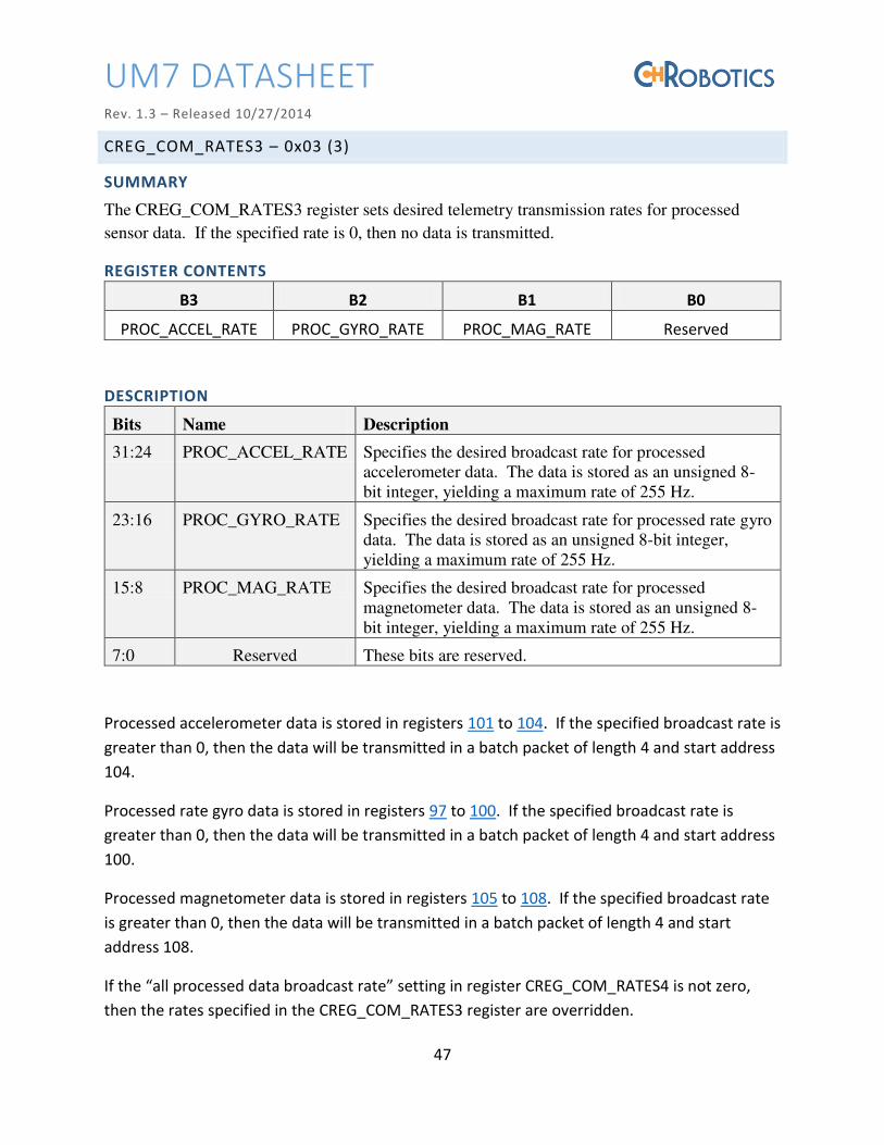
UM7 DATASHEET
Rev. 1.3 – Released 10/27/2014
47
CREG_COM_RATES3 – 0x03 (3)
SUMMARY
The CREG_COM_RATES3 register sets desired telemetry transmission rates for processed
sensor data. If the specified rate is 0, then no data is transmitted.
REGISTER CONTENTS
B3 B2 B1 B0
PROC_ACCEL_RATE PROC_GYRO_RATE PROC_MAG_RATE Reserved
DESCRIPTION
Bits Name Description
31:24 PROC_ACCEL_RATE Specifies the desired broadcast rate for processed accelerometer data. The data is stored as an unsigned 8-bit integer, yielding a maximum rate of 255 Hz.
23:16 PROC_GYRO_RATE Specifies the desired broadcast rate for processed rate gyro data. The data is stored as an unsigned 8-bit integer, yielding a maximum rate of 255 Hz.
15:8 PROC_MAG_RATE Specifies the desired broadcast rate for processed magnetometer data. The data is stored as an unsigned 8-bit integer, yielding a maximum rate of 255 Hz.
7:0 Reserved These bits are reserved.
Processed accelerometer data is stored in registers 101 to 104. If the specified broadcast rate is
greater than 0, then the data will be transmitted in a batch packet of length 4 and start address
104.
Processed rate gyro data is stored in registers 97 to 100. If the specified broadcast rate is
greater than 0, then the data will be transmitted in a batch packet of length 4 and start address
100.
Processed magnetometer data is stored in registers 105 to 108. If the specified broadcast rate
is greater than 0, then the data will be transmitted in a batch packet of length 4 and start
address 108.
If the all p o essed data oad ast ate setti g i egister CREG_COM_RATES4 is not zero,
then the rates specified in the CREG_COM_RATES3 register are overridden.

UM7 DATASHEET
Rev. 1.3 – Released 10/27/2014
48
CREG_COM_RATES4 – 0x04 (4)
SUMMARY
The CREG_COM_RATES4 register sets desired telemetry transmission rates for all processed
dat. If the specified rate is 0, then no data is transmitted.
REGISTER CONTENTS
B3 B2 B1 B0
RES RES RES ALL_PROC_RATE
DESCRIPTION
Bits Name Description
31:24 RES These bits are reserved for future use
23:16 RES These bits are reserved for future use
15:8 RES These bits are reserved for future use
7:0 ALL_PROC_RATE Specifies the desired broadcast rate for raw all processed
data. If set, this overrides the broadcast rate setting for
individual processed data broadcast rates. The data is
stored as an unsigned 8-bit integer, yielding a maximum
rate of 255 Hz.
All processed data comprises registers 97 through 108 (a total of 12 registers). If
ALL_PROC_RATE is non-zero, the processed data will be transmitted as a single packet of batch
length 12, starting at address 97.
CREG_COM_RATES5 – 0x05 (5)
SUMMARY
The CREG_COM_RATES5 register sets desired telemetry transmission rates for quaternions,
Euler Angles, position, and velocity estimates. If the specified rate is 0, then no data is
transmitted.
REGISTER CONTENTS
B3 B2 B1 B0
QUAT_RATE EULER_RATE POSITION_RATE VELOCITY_RATE

UM7 DATASHEET
Rev. 1.3 – Released 10/27/2014
49
DESCRIPTION
Bits Name Description
31:24 QUAT_RATE Specifies the desired broadcast rate for quaternion data.
The data is stored as an unsigned 8-bit integer, yielding a
maximum rate of 255 Hz.
23:16 EULER_RATE Specifies the desired broadcast rate for Euler Angle data.
The data is stored as an unsigned 8-bit integer, yielding a
maximum rate of 255 Hz.
15:8 POSITION_RATE Specifies the desired broadcast rate position. The data is
stored as an unsigned 8-bit integer, yielding a maximum
rate of 255 Hz.
7:0 VELOCITY_RATE Specifies the desired broadcast rate for velocity. The data is
stored as an unsigned 8-bit integer, yielding a maximum
rate of 255 Hz.
Quaternion data is stored in registers 109 to 111. If the specified broadcast rate is greater than
0, then the data will be transmitted in a batch packet with length 3 and start address 109.
Euler Angle data is stored in registers 112 to 116. If the specified broadcast rate is greater than
0, then the data will be transmitted in a batch packet of length 5 and start address 112.
Position data is stored in registers 117 to 120. If the specified broadcast rate is greater than 0,
then the data will be transmitted in a batch packet of length 4 and start address 117.
Velocity data is stored in registers 121 to 124. If the specified broadcast rate is greater than 0,
then the data will be transmitted in a batch packet of length 4 and start address 121.
If the pose oad ast ate setting in register CREG_COM_RATES6 is not zero, then the rates
specified by EULER_RATE and POSITION_RATE are overridden.
CREG_COM_RATES6 – 0x06 (6)
SUMMARY
The CREG_COM_RATES6 register sets desired telemetry transmission rates for pose
(Euler/position packet) and health. If the specified rate is 0, then no data is transmitted.

UM7 DATASHEET
Rev. 1.3 – Released 10/27/2014
50
REGISTER CONTENTS
B3 B2
31 30 29 28 27 26 25 24 23 22 21 20 19 18 17 16
POSE_RATE RESERVED HEALTH_RATE
B1 B0
15 14 13 12 11 10 9 8 7 6 5 4 3 2 1 0
RESERVED
DESCRIPTION
Bits Name Description
31:24 POSE_RATE Specifies the desired broadcast rate for pose (Euler Angle
and position) data. The data is stored as an unsigned 8-bit
integer, yielding a maximum rate of 255 Hz.
23:20 RESERVED These bits are reserved for future use.
19:16 HEALTH_RATE Specifies the desired broadcast rate for the sensor health
packet.
0 = off
1 = 0.125 Hz
2 = 0.25 Hz
3 = 0.5 Hz
4 = 1 Hz
5 = 2 Hz
6 = 4 Hz
7:15 = Unused*
* Will default to 1Hz
15:0 RESERVED These bits are reserved for future use.

UM7 DATASHEET
Rev. 1.3 – Released 10/27/2014
51
Pose data (Euler Angles and position) is stored in registers 112 to 120. If the pose rate is
greater than 0, then pose data will be transmitted in a batch packet with length 9 and start
address 112.
Health data is stored in register address 85. If the health rate is not 0, then health data will be
transmitted as a non-batch packet with address 85.
CREG_COM_RATES7 – 0x07 (7)
SUMMARY
The CREG_COM_RATES7 register sets desired transmission rates for CHR NMEA-style
packets.
REGISTER CONTENTS
B3 B2
31 30 29 28 27 26 25 24 23 22 21 20 19 18 17 16
HEALTH_RATE POSE_RATE ATTITUDE_RATE SENSOR_RATE
B1 B0
15 14 13 12 11 10 9 8 7 6 5 4 3 2 1 0
RATES_RATE GPS_POSE_RATE QUAT_RATE RESERVED
DESCRIPTION
Bits Name Description
31:28 HEALTH_RATE Specifies the desired broadcast rate for CHR NMEA-style
health packet.
0 = off
1 = 1 Hz
2 = 2 Hz
3 = 4 Hz
4 = 5 Hz
5 = 10 Hz
6 = 15 Hz
7 = 20 Hz
UM7 DATASHEET
Rev. 1.3 – Released 10/27/2014
52
8 = 30 Hz
9 = 40 Hz
10 = 50 Hz
11 = 60 Hz
12 = 70 Hz
13 = 80 Hz
14 = 90 Hz
15 = 100 Hz
27:24 POSE_RATE Specifies the desired broadcast rate for CHR NMEA-style
pose (Euler Angle/position) packet.
0 = off
1 = 1 Hz
2 = 2 Hz
3 = 4 Hz
4 = 5 Hz
5 = 10 Hz
6 = 15 Hz
7 = 20 Hz
8 = 30 Hz
9 = 40 Hz
10 = 50 Hz
11 = 60 Hz
12 = 70 Hz
13 = 80 Hz
14 = 90 Hz
15 = 100 Hz
23:20 ATTITUDE_RATE Specifies the desired broadcast rate for CHR NMEA-style
attitude packet.
0 = off
1 = 1 Hz
UM7 DATASHEET
Rev. 1.3 – Released 10/27/2014
53
2 = 2 Hz
3 = 4 Hz
4 = 5 Hz
5 = 10 Hz
6 = 15 Hz
7 = 20 Hz
8 = 30 Hz
9 = 40 Hz
10 = 50 Hz
11 = 60 Hz
12 = 70 Hz
13 = 80 Hz
14 = 90 Hz
15 = 100 Hz
19:16 SENSOR_RATE Specifies the desired broadcast rate for CHR NMEA-style
sensor data packet
0 = off
1 = 1 Hz
2 = 2 Hz
3 = 4 Hz
4 = 5 Hz
5 = 10 Hz
6 = 15 Hz
7 = 20 Hz
8 = 30 Hz
9 = 40 Hz
10 = 50 Hz
11 = 60 Hz
12 = 70 Hz
13 = 80 Hz
14 = 90 Hz

UM7 DATASHEET
Rev. 1.3 – Released 10/27/2014
54
15 = 100 Hz
15:12 RATES_RATE Specifies the desired broadcast rate for CHR NMEA-style
rate data packet.
0 = off
1 = 1 Hz
2 = 2 Hz
3 = 4 Hz
4 = 5 Hz
5 = 10 Hz
6 = 15 Hz
7 = 20 Hz
8 = 30 Hz
9 = 40 Hz
10 = 50 Hz
11 = 60 Hz
12 = 70 Hz
13 = 80 Hz
14 = 90 Hz
15 = 100 Hz
11:8 GPS_POSE_RATE Specifies the desired broadcast rate for CHR NMEA-style
GPS pose packet.
0 = off
1 = 1 Hz
2 = 2 Hz
3 = 4 Hz
4 = 5 Hz
5 = 10 Hz
6 = 15 Hz
7 = 20 Hz
8 = 30 Hz

UM7 DATASHEET
Rev. 1.3 – Released 10/27/2014
55
9 = 40 Hz
10 = 50 Hz
11 = 60 Hz
12 = 70 Hz
13 = 80 Hz
14 = 90 Hz
15 = 100 Hz
7:4 QUAT_RATE Specifies the desired broadcast rate for CHR NMEA-style
quaternion packet.
0 = off
1 = 1 Hz
2 = 2 Hz
3 = 4 Hz
4 = 5 Hz
5 = 10 Hz
6 = 15 Hz
7 = 20 Hz
8 = 30 Hz
9 = 40 Hz
10 = 50 Hz
11 = 60 Hz
12 = 70 Hz
13 = 80 Hz
14 = 90 Hz
15 = 100 Hz
3:0 RES These bits are reserved.
CREG_MISC_SETTINGS – 0x08 (8)
SUMMARY
This register contains miscellaneous filter and sensor control options.

UM7 DATASHEET
Rev. 1.3 – Released 10/27/2014
56
REGISTER CONTENTS
B3 B2
31 30 29 28 27 26 25 24 23 22 21 20 19 18 17 16
RESERVED
B1 B0
15 14 13 12 11 10 9 8 7 6 5 4 3 2 1 0
RESERVED PPS RESERVED ZG Q MAG
DESCRIPTION
Bits Name Description
31:9 RESERVED These bits are reserved for future use
8 PPS If set, this bit causes the TX2 pin on the IO Expansion header
to be used as the PPS input from an external GPS module.
PPS pulses will then be used to synchronize the system clock
to UTC time of day.
7:3 RESERVED These bits are reserved for future use
2 ZG If set, this bit causes the UM7 to attempt to measure the
rate gyro bias on startup. The sensor must be stationary on
startup for this feature to work properly.
1 Q If this bit is set, the sensor will run in quaternion mode
instead of Euler Angle mode.
0 MAG If set, the magnetometer will be used in state updates.
CREG_HOME_NORTH – 0x09 (9)
SUMMARY
This register sets the north home latitude in degrees, used to convert GPS coordinates to
position in meters from home.
REGISTER CONTENTS
B3 B2 B1 B0
32-bit IEEE Floating Point Value

UM7 DATASHEET
Rev. 1.3 – Released 10/27/2014
57
CREG_HOME_EAST – 0x0A (10)
SUMMARY
This register sets the east home longitude in degrees, used to convert GPS coordinates to
position in meters from home.
REGISTER CONTENTS
B3 B2 B1 B0
32-bit IEEE Floating Point Value
CREG_HOME_UP – 0x0B (11)
SUMMARY
This register sets the home altitude in meters. Used to convert GPS coordinates to position in
meters from home.
REGISTER CONTENTS
B3 B2 B1 B0
32-bit IEEE Floating Point Value
CREG_GYRO_TRIM_X – 0x0C (12)
SUMMARY
This register sets the x-axis rate gyro trim, which is used to add additional bias compensation
for the rate gyros during calls to the ZERO_GYRO_BIAS command.
REGISTER CONTENTS
B3 B2 B1 B0
32-bit IEEE Floating Point Value
CREG_GYRO_TRIM_Y – 0x0D (13)
SUMMARY
UM7 DATASHEET
Rev. 1.3 – Released 10/27/2014
58
This register sets the y-axis rate gyro trim, which is used to add additional bias compensation
for the rate gyros during calls to the ZERO_GYRO_BIAS command.
REGISTER CONTENTS
B3 B2 B1 B0
32-bit IEEE Floating Point Value
CREG_GYRO_TRIM_Z – 0x0E (14)
SUMMARY
This register sets the z-axis rate gyro trim, which is used to add additional bias compensation
for the rate gyros during calls to the ZERO_GYRO_BIAS command.
REGISTER CONTENTS
B3 B2 B1 B0
32-bit IEEE Floating Point Value
CREG_MAG_CAL1_1 to CREG_MAG_CAL3_3 – 0x0F (15) to 0x17 (23)
SUMMARY
These registers store the 9 entries into a 3x3 matrix that is used to perform soft-iron calibration
of the magnetometer on the device. These terms can be computed by performing
magnetometer calibration with the CHR Serial Interface.
REGISTER CONTENTS
B3 B2 B1 B0
32-bit IEEE Floating Point Value
CREG_MAG_BIAS_X – 0x18 (24)
SUMMARY
This registers stores a bias term for the magnetometer x-axis for hard-iron calibration. This
term can be computed by performing magnetometer calibration with the CHR Serial Interface.

UM7 DATASHEET
Rev. 1.3 – Released 10/27/2014
59
REGISTER CONTENTS
B3 B2 B1 B0
32-bit IEEE Floating Point Value
CREG_MAG_BIAS_Y – 0x19 (25)
SUMMARY
This registers stores a bias term for the magnetometer y-axis for hard-iron calibration. This
term can be computed by performing magnetometer calibration with the CHR Serial Interface.
REGISTER CONTENTS
B3 B2 B1 B0
32-bit IEEE Floating Point Value
CREG_MAG_BIAS_Z – 0x1A (26)
SUMMARY
This registers stores a bias term for the magnetometer z-axis for hard-iron calibration. This
term can be computed by performing magnetometer calibration with the CHR Serial Interface.
REGISTER CONTENTS
B3 B2 B1 B0
32-bit IEEE Floating Point Value

UM7 DATASHEET
Rev. 1.3 – Released 10/27/2014
60
DATA REGISTERS
DREG_HEALTH – 0x55 (85)
SUMMARY
The health register reports the current status of the GPS module and the other sensors on the
UM7. Monitoring the health register is the easiest way to monitor the quality of the GPS lock
and to watch for other problems that could affect the behavior of the UM7.
REGISTER CONTENTS
B3 B2
31 30 29 28 27 26 25 24 23 22 21 20 19 18 17 16
SATS_USED HDOP
B1 B0
15 14 13 12 11 10 9 8 7 6 5 4 3 2 1 0
SATS_IN_VIEW RES OVF RES MG_N ACC_N ACCEL GYRO MAG GPS
DESCRIPTION
Bits Name Description
31:26 SATS_USED Reports the number of satellites used in the position
solution.
25:16 HDOP Reports the horizontal dilution of precision (HDOP) reported
by the GPS. The actual HDOP value is equal to the contents
of the HDOP bits divided by 10.
15:10 SATS_IN_VIEW Reports the number of satellites in view.
9 RES This bit is reserved.
8 OVF Overflow bit. This bit is set if the UM7 is attempting to
transmit data over the serial port faster than is allowed
given the baud-rate. If this bit is set, reduce broadcast rates
in the COM_RATES registers.
7:6 RES These bits are reserved.
5 MG_N This bit is set if the sensor detects that the norm of the
magnetometer measurement is too far away from 1.0 to be

UM7 DATASHEET
Rev. 1.3 – Released 10/27/2014
61
trusted. Usually indicates bad calibration, local field
distortions, or both.
4 ACC_N This bit is set if the sensor detects that the norm of the
accelerometer measurement is too far away from 1G to be
used (i.e. during aggressive acceleration or high vibration).
3 ACCEL This bit will be set if the accelerometer fails to initialize on
startup.
2 GYRO This bit will be set if the rate gyro fails to initialize on
startup.
1 MAG This bit will be set if the magnetometer fails to initialize on
startup.
0 GPS This bit is set if the GPS fails to send a packet for more than
two seconds. If a GPS packet is ever received, this bit is
cleared.
DREG_GYRO_RAW_XY – 0x56 (86)
SUMMARY
Contains raw X and Y axis rate gyro data
REGISTER CONTENTS
B3 B2 B1 B0
Gyro X s o ple e t -bit integer) Gyro Y s o ple e t -bit integer)
DREG_GYRO_RAW_Z – 0x57 (87)
SUMMARY
Contains raw Z axis rate gyro data
REGISTER CONTENTS
B3 B2 B1 B0
Gyro Z s o ple e t -bit integer) RES

UM7 DATASHEET
Rev. 1.3 – Released 10/27/2014
62
DREG_GYRO_RAW_TIME – 0x58 (88)
SUMMARY
Contains time at which the last rate gyro data was acquired.
REGISTER CONTENTS
B3 B2 B1 B0
Gyro Time (IEEE Floating Point)
DREG_ACCEL_RAW_XY – 0x59 (89)
SUMMARY
Contains raw X and Y axis accelerometer data.
REGISTER CONTENTS
B3 B2 B1 B0
Accel X s o ple e t -bit integer) Accel Y s o ple e t -bit integer)
DREG_ACCEL_RAW_Z – 0x5A (90)
SUMMARY
Contains raw Z axis accelerometer data
REGISTER CONTENTS
B3 B2 B1 B0
Accel ) s o ple e t -bit integer) RES
DREG_ACCEL_RAW_TIME – 0x5B (91)
SUMMARY
Contains time at which the last accelerometer data was acquired.
REGISTER CONTENTS
B3 B2 B1 B0
Accel Time (IEEE Floating Point)

UM7 DATASHEET
Rev. 1.3 – Released 10/27/2014
63
DREG_MAG_RAW_XY – 0x5C (92)
SUMMARY
Contains raw X and Y axis magnetometer data.
REGISTER CONTENTS
B3 B2 B1 B0
Mag X s o ple e t -bit integer) Mag Y s o ple e t -bit integer)
DREG_MAG_RAW_Z – 0x5D (93)
SUMMARY
Contains raw Z axis magnetometer data
REGISTER CONTENTS
B3 B2 B1 B0
Mag ) s o ple e t -bit integer) RES
DREG_MAG_RAW_TIME – 0x5E (94)
SUMMARY
Contains time at which the last magnetometer data was acquired.
REGISTER CONTENTS
B3 B2 B1 B0
Mag Time (IEEE Floating Point)
DREG_TEMPERATURE – 0x5F (95)
SUMMARY
Contains the temperature output of the onboard temperature sensor.
UM7 DATASHEET
Rev. 1.3 – Released 10/27/2014
64
REGISTER CONTENTS
B3 B2 B1 B0
Temperature in degrees C (IEEE Floating Point)
DREG_TEMPERATURE_TIME – 0x60 (96)
SUMMARY
Contains time at which the last temperature was acquired.
REGISTER CONTENTS
B3 B2 B1 B0
Temperature time (IEEE Floating Point)
DREG_GYRO_PROC_X – 0x61 (97)
SUMMARY
Contains the actual measured angular rate in degrees/s after calibration has been applied.
REGISTER CONTENTS
B3 B2 B1 B0
Gyro X (IEEE Floating Point)
DREG_GYRO_PROC_Y – 0x62 (98)
SUMMARY
Contains the actual measured angular rate in degrees/s after calibration has been applied.
REGISTER CONTENTS

UM7 DATASHEET
Rev. 1.3 – Released 10/27/2014
65
B3 B2 B1 B0
Gyro Y (IEEE Floating Point)
DREG_GYRO_PROC_Z – 0x63 (99)
SUMMARY
Contains the actual measured angular rate in degrees/s after calibration has been applied.
REGISTER CONTENTS
B3 B2 B1 B0
Gyro Z (IEEE Floating Point)
DREG_GYRO_PROC_TIME – 0x64 (100)
SUMMARY
Contains the time at which the last rate gyro data was measured.
REGISTER CONTENTS
B3 B2 B1 B0
Gyro Time (IEEE Floating Point)
DREG_ACCEL_PROC_X – 0x65 (101)
SUMMARY
Contains the actual measured acceleration in m/s/s after calibration has been applied.
REGISTER CONTENTS
B3 B2 B1 B0
Accel X (IEEE Floating Point)
DREG_ACCEL_PROC_Y – 0x66 (102)
SUMMARY
Contains the actual measured acceleration in m/s/s after calibration has been applied.
UM7 DATASHEET
Rev. 1.3 – Released 10/27/2014
66
REGISTER CONTENTS
B3 B2 B1 B0
Accel Y (IEEE Floating Point)
DREG_ACCEL_PROC_Z – 0x67 (103)
SUMMARY
Contains the actual measured acceleration in m/s/s after calibration has been applied.
REGISTER CONTENTS
B3 B2 B1 B0
Accel Z (IEEE Floating Point)
DREG_ACCEL_PROC_TIME – 0x68 (104)
SUMMARY
Contains the time at which the acceleration was measured.
REGISTER CONTENTS
B3 B2 B1 B0
Accel Time (IEEE Floating Point)
DREG_MAG_PROC_X – 0x69 (105)
SUMMARY
Contains the actual measured magnetic field after calibration has been applied.
REGISTER CONTENTS
UM7 DATASHEET
Rev. 1.3 – Released 10/27/2014
67
B3 B2 B1 B0
Mag X (IEEE Floating Point)
DREG_MAG_PROC_Y – 0x6A (106)
SUMMARY
Contains the actual measured magnetic field after calibration has been applied.
REGISTER CONTENTS
B3 B2 B1 B0
Mag Y (IEEE Floating Point)
DREG_MAG_PROC_Z – 0x6B (107)
SUMMARY
Contains the actual measured magnetic field after calibration has been applied.
REGISTER CONTENTS
B3 B2 B1 B0
Mag Z (IEEE Floating Point)
DREG_MAG_PROC_TIME – 0x6C (108)
SUMMARY
Contains the time at which magnetometer data was acquired.
REGISTER CONTENTS
B3 B2 B1 B0
Mag Time (IEEE Floating Point)
DREG_QUAT_AB – 0x6D (109)
SUMMARY
Contains the first two components of the estimated quaternion attitude.

UM7 DATASHEET
Rev. 1.3 – Released 10/27/2014
68
REGISTER CONTENTS
B3 B2 B1 B0
Quat A Quat B
DESCRIPTION
Bits Name Description
31:16 Quat A First quaternion component. Stored as a 16-bit signed
integer. To get the actual value, divide by 29789.09091.
15:0 Quat B Second quaternion component. Stored as a 16-bit signed
integer. To get the actual value, divide by 29789.09091.
DREG_QUAT_CD – 0x6E (110)
SUMMARY
Contains the second two components of the estimated quaternion attitude.
REGISTER CONTENTS
B3 B2 B1 B0
Quat C Quat D
DESCRIPTION
Bits Name Description
31:16 Quat C Third quaternion component. Stored as a 16-bit signed
integer. To get the actual value, divide by 29789.09091.
15:0 Quat D Fourth quaternion component. Stored as a 16-bit signed
integer. To get the actual value, divide by 29789.09091.
DREG_QUAT_TIME – 0x6F (111)
SUMMARY
Contains the time that the quaternion attitude was measured
REGISTER CONTENTS

UM7 DATASHEET
Rev. 1.3 – Released 10/27/2014
69
B3 B2 B1 B0
Quaternion Time (IEEE Floating Point)
DREG_EULER_PHI_THETA – 0x70 (112)
SUMMARY
Contains the pitch and roll angle estimates.
REGISTER CONTENTS
B3 B2 B1 B0
Phi (roll) Theta (Pitch)
DESCRIPTION
Bits Name Description
31:16 Phi (roll) Roll angle. Stored as a 16-bit signed integer. To get the
actual value, divide by 91.02222.
15:0 Theta (pitch) Pitch angle. Stored as a 16-bit signed integer. To get the
actual value, divide by 91.02222.
DREG_EULER_PSI – 0x71 (113)
SUMMARY
Contains the yaw angle estimate.
REGISTER CONTENTS
B3 B2 B1 B0
Psi (yaw) Unused
DESCRIPTION
Bits Name Description
31:16 Psi (yaw) Yaw angle. Stored as a 16-bit signed integer. To get the
actual value, divide by 91.02222.
15:0 Unused These bits are unused
UM7 DATASHEET
Rev. 1.3 – Released 10/27/2014
70
DREG_EULER_PHI_THETA_DOT – 0x72 (114)
SUMMARY
Contains the pitch and roll rate estimates.
REGISTER CONTENTS
B3 B2 B1 B0
Roll rate Pitch rate
DESCRIPTION
Bits Name Description
31:16 Roll rate Roll rate. Stored as a 16-bit signed integer. To get the
actual value in degrees per second, divide by 16.0.
15:0 Pitch rate Pitch angle. Stored as a 16-bit signed integer. To get the
actual value in degrees per second, divide by 16.0.
DREG_EULER_PSI_DOT – 0x73 (115)
SUMMARY
Contains the yaw rate estimate.
REGISTER CONTENTS
B3 B2 B1 B0
Yaw rate Unused
DESCRIPTION
Bits Name Description
31:16 Yaw rate Yaw rate. Stored as a 16-bit signed integer. To get the
actual value in degrees per second, divide by 16.0.

UM7 DATASHEET
Rev. 1.3 – Released 10/27/2014
71
15:0 Unused These bits are unused
DREG_EULER_TIME – 0x74 (116)
SUMMARY
Contains the time that the Euler Angles were measured.
REGISTER CONTENTS
B3 B2 B1 B0
Euler Time (IEEE Floating Point)
DREG_POSITION_N – 0x75 (117)
SUMMARY
Contains the measured north position in meters from the latitude specified in
CREG_HOME_NORTH.
REGISTER CONTENTS
B3 B2 B1 B0
North Position (IEEE Floating Point)
DREG_POSITION_E – 0x76 (118)
SUMMARY
Contains the measured east position in meters from the longitude specified in
CREG_HOME_EAST.
REGISTER CONTENTS
B3 B2 B1 B0
East Position (IEEE Floating Point)

UM7 DATASHEET
Rev. 1.3 – Released 10/27/2014
72
DREG_POSITION_UP – 0x77 (119)
SUMMARY
Contains the measured altitude in meters from the altitude specified in CREG_HOME_UP.
REGISTER CONTENTS
B3 B2 B1 B0
Altitude (IEEE Floating Point)
DREG_POSITION_TIME – 0x78 (120)
SUMMARY
Contains the time at which the position was acquired.
REGISTER CONTENTS
B3 B2 B1 B0
Position Time (IEEE Floating Point)
DREG_VELOCITY_N – 0x79 (121)
SUMMARY
Contains the measured north velocity in m/s.
REGISTER CONTENTS
B3 B2 B1 B0
North Velocity (IEEE Floating Point)
DREG_VELOCITY_E – 0x7A (122)
SUMMARY
Contains the measured east velocity in m/s.
UM7 DATASHEET
Rev. 1.3 – Released 10/27/2014
73
REGISTER CONTENTS
B3 B2 B1 B0
East Velocity (IEEE Floating Point)
DREG_VELOCITY_UP – 0x7B (123)
SUMMARY
Contains the measured altitude velocity in m/s.
REGISTER CONTENTS
B3 B2 B1 B0
Altitude Velocity (IEEE Floating Point)
DREG_VELOCITY_TIME – 0x7C (124)
SUMMARY
Contains the time at which the velocity was measured.
REGISTER CONTENTS
B3 B2 B1 B0
Velocity Time (IEEE Floating Point)
DREG_GPS_LATITUDE – 0x7D (125)
SUMMARY
Contains the GPS-reported latitude in degrees.
REGISTER CONTENTS
B3 B2 B1 B0
GPS Latitude (IEEE Floating Point)
DREG_GPS_LONGITUDE – 0x7E (126)
SUMMARY
Contains the GPS-reported longitude in degrees.

UM7 DATASHEET
Rev. 1.3 – Released 10/27/2014
74
REGISTER CONTENTS
B3 B2 B1 B0
GPS Longitude (IEEE Floating Point)
DREG_GPS_ALTITUDE – 0x7F (127)
SUMMARY
Contains the GPS-reported altitude in meters.
REGISTER CONTENTS
B3 B2 B1 B0
GPS Altitude (IEEE Floating Point)
DREG_GPS_COURSE – 0x80 (128)
SUMMARY
Contains the GPS-reported course in degrees.
REGISTER CONTENTS
B3 B2 B1 B0
GPS Course (IEEE Floating Point)
DREG_GPS_SPEED – 0x81 (129)
SUMMARY
Contains the GPS-reported speed in m/s.
REGISTER CONTENTS
B3 B2 B1 B0
GPS Speed (IEEE Floating Point)
DREG_GPS_TIME – 0x82 (130)
SUMMARY
UM7 DATASHEET
Rev. 1.3 – Released 10/27/2014
75
Contains the GPS-reported time in seconds from the last epoch.
REGISTER CONTENTS
B3 B2 B1 B0
GPS Time (IEEE Floating Point)
DREG_GPS_SAT_1_2 – 0x83 (131)
SUMMARY
Contains satellite ID and SNR for satellites 1 and 2.
REGISTER CONTENTS
B3 B2 B1 B0
Sat1 ID Sat1 SNR Sat2 ID Sat2 SNR
DESCRIPTION
Bits Name Description
31:24 Sat1 ID ID of satellite
23:16 Sat1 SNR Signal-to-Noise Ratio of satellite as reported by GPS receiver
15:8 Sat2 ID ID of satellite
7:0 Sat2 SNR Signal-to-Noise Ratio of satellite as reported by GPS receiver
DREG_GPS_SAT_3_4 – 0x84 (132)
SUMMARY
Contains satellite ID and SNR for satellites 3 and 4.
REGISTER CONTENTS
B3 B2 B1 B0
Sat3 ID Sat3 SNR Sat4 ID Sat4 SNR
DESCRIPTION
Bits Name Description

UM7 DATASHEET
Rev. 1.3 – Released 10/27/2014
76
31:24 Sat3 ID ID of satellite
23:16 Sat3 SNR Signal-to-Noise Ratio of satellite as reported by GPS receiver
15:8 Sat4 ID ID of satellite
7:0 Sat5 SNR Signal-to-Noise Ratio of satellite as reported by GPS receiver
DREG_GPS_SAT_5_6 – 0x85 (133)
SUMMARY
Contains satellite ID and SNR for satellites 5 and 6.
REGISTER CONTENTS
B3 B2 B1 B0
Sat5 ID Sat5 SNR Sat6 ID Sat6 SNR
DESCRIPTION
Bits Name Description
31:24 Sat5 ID ID of satellite
23:16 Sat5 SNR Signal-to-Noise Ratio of satellite as reported by GPS receiver
15:8 Sat6 ID ID of satellite
7:0 Sat6 SNR Signal-to-Noise Ratio of satellite as reported by GPS receiver
DREG_GPS_SAT_7_8 – 0x86 (134)
SUMMARY
Contains satellite ID and SNR for satellites 7 and 8.
REGISTER CONTENTS
B3 B2 B1 B0
Sat7 ID Sat7 SNR Sat8 ID Sat8 SNR
DESCRIPTION
Bits Name Description

UM7 DATASHEET
Rev. 1.3 – Released 10/27/2014
77
31:24 Sat7 ID ID of satellite
23:16 Sat7 SNR Signal-to-Noise Ratio of satellite as reported by GPS receiver
15:8 Sat8 ID ID of satellite
7:0 Sat8 SNR Signal-to-Noise Ratio of satellite as reported by GPS receiver
DREG_GPS_SAT_9_10 – 0x87 (135)
SUMMARY
Contains satellite ID and SNR for satellites 9 and 10.
REGISTER CONTENTS
B3 B2 B1 B0
Sat9 ID Sat9 SNR Sat10 ID Sat10 SNR
DESCRIPTION
Bits Name Description
31:24 Sat9 ID ID of satellite
23:16 Sat9 SNR Signal-to-Noise Ratio of satellite as reported by GPS receiver
15:8 Sat10 ID ID of satellite
7:0 Sat10 SNR Signal-to-Noise Ratio of satellite as reported by GPS receiver
DREG_GPS_SAT_11_12 – 0x88 (136)
SUMMARY
Contains satellite ID and SNR for satellites 11 and 12.
REGISTER CONTENTS
B3 B2 B1 B0
Sat11 ID Sat11 SNR Sat12 ID Sat12 SNR
DESCRIPTION
Bits Name Description
UM7 DATASHEET
Rev. 1.3 – Released 10/27/2014
78
31:24 Sat11 ID ID of satellite
23:16 Sat11 SNR Signal-to-Noise Ratio of satellite as reported by GPS receiver
15:8 Sat12 ID ID of satellite
7:0 Sat12 SNR Signal-to-Noise Ratio of satellite as reported by GPS receiver
COMMANDS
GET_FW_REVISION – 0xAA (170)
Causes the UM7 to transmit a packet containing the firmware revision string. The firmware
revision is a four-byte character sequence. The first firmware release version for the UM7, for
e a ple, as O‘ A .
The address of the packet will be 0xAA. The data section of the packet will contain four bytes.
FLASH_COMMIT – 0xAB (171)
Causes the UM7 to write all configuration settings to FLASH so that they will remain when the
power is cycled.
RESET_TO_FACTORY – 0xAC (172)
Causes the UM7 to load default factory settings.
ZERO_GYROS – 0xAD (173)
Causes the UM7 to measure the gyro outputs and set the output trim registers to compensate
for any non-zero bias. The UM7 should be kept stationary while the zero operation is
underway.
SET_HOME_POSITION – 0xAE (174)
Sets the current GPS latitude, longitude, and altitude as the home position. All future positions
will be referenced to the current GPS position.
SET_MAG_REFERENCE – 0xB0 (176)
Sets the current GPS latitude, longitude, and altitude as the home position. All future positions
will be referenced to the current GPS position.

UM7 DATASHEET
Rev. 1.3 – Released 10/27/2014
79
RESET_EKF – 0xB3 (179)
Resets the filter.
DISCLAIMER
This document is provided as reference only. Typical device specifications must be evaluated
by the end-user. CH Robotics reserves the right to modify this document and the products it
describes without notice.
CH Robotics products are not intended for use in weapons systems, aircraft, life-saving or life-
sustaining systems, automobiles, or any other application where failure could result in injury,
death, property damage, or environmental damage.
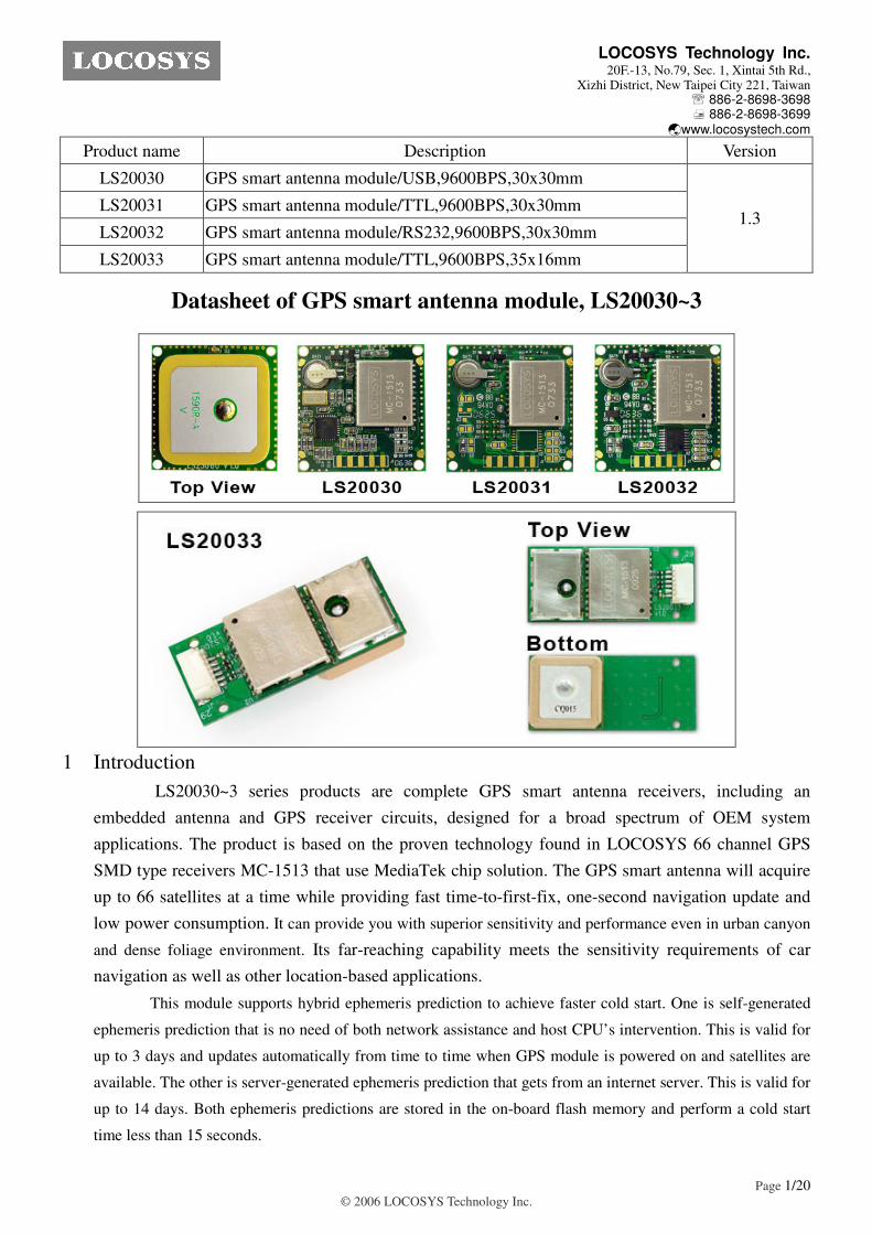
LOCOSYS Technology Inc. 20F.-13, No.79, Sec. 1, Xintai 5th Rd.,
Xizhi District, New Taipei City 221, Taiwan 886-2-8698-3698 886-2-8698-3699
www.locosystech.com
Page 1/20
© 2006 LOCOSYS Technology Inc.
Product name Description Version
LS20030 GPS smart antenna module/USB,9600BPS,30x30mm
LS20031 GPS smart antenna module/TTL,9600BPS,30x30mm
LS20032 GPS smart antenna module/RS232,9600BPS,30x30mm
LS20033 GPS smart antenna module/TTL,9600BPS,35x16mm
1.3
Datasheet of GPS smart antenna module, LS20030~3
1 Introduction
LS20030~3 series products are complete GPS smart antenna receivers, including an
embedded antenna and GPS receiver circuits, designed for a broad spectrum of OEM system
applications. The product is based on the proven technology found in LOCOSYS 66 channel GPS
SMD type receivers MC-1513 that use MediaTek chip solution. The GPS smart antenna will acquire
up to 66 satellites at a time while providing fast time-to-first-fix, one-second navigation update and
low power consumption. It can provide you with superior sensitivity and performance even in urban canyon
and dense foliage environment. Its far-reaching capability meets the sensitivity requirements of car
navigation as well as other location-based applications.
This module supports hybrid ephemeris prediction to achieve faster cold start. One is self-generated
ephemeris prediction that is no need of both network assistance and host CPU’s intervention. This is valid for
up to 3 days and updates automatically from time to time when GPS module is powered on and satellites are
available. The other is server-generated ephemeris prediction that gets from an internet server. This is valid for
up to 14 days. Both ephemeris predictions are stored in the on-board flash memory and perform a cold start
time less than 15 seconds.

LOCOSYS Technology Inc. 20F.-13, No.79, Sec. 1, Xintai 5th Rd.,
Xizhi District, New Taipei City 221, Taiwan 886-2-8698-3698 886-2-8698-3699
www.locosystech.com
Page 2/20
© 2006 LOCOSYS Technology Inc.
2 Features MediaTek high sensitivity solution
Support 66-channel GPS
Low power consumption
Fast TTFF at low signal level
Built-in 12 multi-tone active interference canceller
Free hybrid ephemeris prediction to achieve faster cold start
Built-in data logger
Up to 10 Hz update rate
Capable of SBAS (WAAS, EGNOS, MSAS, GAGAN)
Support Japan QZSS
Indoor and outdoor multi-path detection and compensation
Build-in micro battery to reserve system data for rapid satellite acquisition (not in LS20033)
LED indicator for GPS fix or not fix (not in LS20033)
3 Application Personal positioning and navigation
Automotive navigation
Marine navigation
Fig 3-1 System block diagram of LS20030

LOCOSYS Technology Inc. 20F.-13, No.79, Sec. 1, Xintai 5th Rd.,
Xizhi District, New Taipei City 221, Taiwan 886-2-8698-3698 886-2-8698-3699
www.locosystech.com
Page 3/20
© 2006 LOCOSYS Technology Inc.
Fig 3-2 System block diagram of LS20031
Fig 3-3 System block diagram of LS20032
Fig 3-4 System block diagram of LS20033

LOCOSYS Technology Inc. 20F.-13, No.79, Sec. 1, Xintai 5th Rd.,
Xizhi District, New Taipei City 221, Taiwan 886-2-8698-3698 886-2-8698-3699
www.locosystech.com
Page 4/20
© 2006 LOCOSYS Technology Inc.
4 GPS receiver
Chip MediaTek MT3339
Frequency L1 1575.42MHz, C/A code
Channels Support 66 channels (22 Tracking, 66 Acquisition)
Update rate 1Hz default, up to 10Hz
Hot start (Open Sky) < 1s (typical)
32s (typical) without AGPS Acquisition Time Cold Start (Open Sky)
<15s (typical) with AGPS (hybrid ephemeris prediction)
Autonomous 3m (2D RMS) Position Accuracy
SBAS 2.5m (depends on accuracy of correction data)
Datum WGS-84 (default)
Max. Altitude < 50,000 m
Max. Velocity < 515 m/s
Protocol Support NMEA 0183 ver 3.01 9600 bps(1), 8 data bits, no parity, 1 stop bits (default)
1Hz: GGA, GLL, GSA, GSV, RMC, VTG
Note 1: Both baud rate and output message rate are configurable to be factory default.
5 Software interface
5.1 NMEA output message Table 5.1-1 NMEA output message
NMEA record Description
GGA Global positioning system fixed data
GLL Geographic position - latitude/longitude
GSA GNSS DOP and active satellites
GSV GNSS satellites in view
RMC Recommended minimum specific GNSS data
VTG Course over ground and ground speed
GGA--- Global Positioning System Fixed Data
Table 5.1-2 contains the values for the following example:
$GPGGA,053740.000,2503.6319,N,12136.0099,E,1,08,1.1,63.8,M,15.2,M,,0000*64
Table5.1- 2 GGA Data Format
Name Example Units Description
Message ID $GPGGA GGA protocol header
UTC Time 053740.000 hhmmss.sss
Latitude 2503.6319 ddmm.mmmm

LOCOSYS Technology Inc. 20F.-13, No.79, Sec. 1, Xintai 5th Rd.,
Xizhi District, New Taipei City 221, Taiwan 886-2-8698-3698 886-2-8698-3699
www.locosystech.com
Page 5/20
© 2006 LOCOSYS Technology Inc.
N/S indicator N N=north or S=south
Longitude 12136.0099 dddmm.mmmm
E/W Indicator E E=east or W=west
Position Fix Indicator 1 See Table 5.1-3
Satellites Used 08 Range 0 to 12
HDOP 1.1 Horizontal Dilution of Precision
MSL Altitude 63.8 mters
Units M mters
Geoid Separation 15.2 mters
Units M mters
Age of Diff. Corr. second Null fields when DGPS is not used
Diff. Ref. Station ID 0000
Checksum *64
<CR> <LF> End of message termination
Table 5.1-3 Position Fix Indicators
Value Description
0 Fix not available or invalid
1 GPS SPS Mode, fix valid
2 Differential GPS, SPS Mode, fix valid
3-5 Not supported
6 Dead Reckoning Mode, fix valid
GLL--- Geographic Position – Latitude/Longitude
Table 5.1-4 contains the values for the following example:
$GPGLL,2503.6319,N,12136.0099,E,053740.000,A,A*52
Table 5.1-4 GLL Data Format
Name Example Units Description
Message ID $GPGLL GLL protocol header
Latitude 2503.6319 ddmm.mmmm
N/S indicator N N=north or S=south
Longitude 12136.0099 dddmm.mmmm
E/W indicator E E=east or W=west
UTC Time 053740.000 hhmmss.sss
Status A A=data valid or V=data not valid
Mode A A=autonomous, D=DGPS, E=DR, N=Data not valid,
R=Coarse Position, S=Simulator
LOCOSYS Technology Inc. 20F.-13, No.79, Sec. 1, Xintai 5th Rd.,
Xizhi District, New Taipei City 221, Taiwan 886-2-8698-3698 886-2-8698-3699
www.locosystech.com
Page 6/20
© 2006 LOCOSYS Technology Inc.
Checksum *52
<CR> <LF> End of message termination
GSA---GNSS DOP and Active Satellites
Table 5.1-5 contains the values for the following example:
$GPGSA,A,3,24,07,17,11,28,08,20,04,,,,,2.0,1.1,1.7*35
Table 5.1-5 GSA Data Format
Name Example Units Description
Message ID $GPGSA GSA protocol header
Mode 1 A See Table 5.1-6
Mode 2 3 See Table 5.1-7
ID of satellite used 24 Sv on Channel 1
ID of satellite used 07 Sv on Channel 2
…. ….
ID of satellite used Sv on Channel 12
PDOP 2.0 Position Dilution of Precision
HDOP 1.1 Horizontal Dilution of Precision
VDOP 1.7 Vertical Dilution of Precision
Checksum *35
<CR> <LF> End of message termination
Table 5.1-6 Mode 1
Value Description
M Manual- forced to operate in 2D or 3D mode
A Automatic-allowed to automatically switch 2D/3D
Table 5.1-7 Mode 2
Value Description
1 Fix not available
2 2D
3 3D
GSV---GNSS Satellites in View
Table 5.1-8 contains the values for the following example:
$GPGSV,3,1,12,28,81,285,42,24,67,302,46,31,54,354,,20,51,077,46*73
$GPGSV,3,2,12,17,41,328,45,07,32,315,45,04,31,250,40,11,25,046,41*75
$GPGSV,3,3,12,08,22,214,38,27,08,190,16,19,05,092,33,23,04,127,*7B
Table 5.1-8 GSV Data Format
Name Example Units Description

LOCOSYS Technology Inc. 20F.-13, No.79, Sec. 1, Xintai 5th Rd.,
Xizhi District, New Taipei City 221, Taiwan 886-2-8698-3698 886-2-8698-3699
www.locosystech.com
Page 7/20
© 2006 LOCOSYS Technology Inc.
Message ID $GPGSV GSV protocol header
Total number of messages1 3 Range 1 to 4
Message number1 1 Range 1 to 4
Satellites in view 12
Satellite ID 28 Channel 1 (Range 01 to 196)
Elevation 81 degrees Channel 1 (Range 00 to 90)
Azimuth 285 degrees Channel 1 (Range 000 to 359)
SNR (C/No) 42 dB-Hz Channel 1 (Range 00 to 99, null when not tracking)
Satellite ID 20 Channel 4 (Range 01 to 32)
Elevation 51 degrees Channel 4 (Range 00 to 90)
Azimuth 077 degrees Channel 4 (Range 000 to 359)
SNR (C/No) 46 dB-Hz Channel 4 (Range 00 to 99, null when not tracking)
Checksum *73
<CR> <LF> End of message termination
1. Depending on the number of satellites tracked multiple messages of GSV data may be required.
RMC---Recommended Minimum Specific GNSS Data
Table 5.1-9 contains the values for the following example:
$GPRMC,053740.000,A,2503.6319,N,12136.0099,E,2.69,79.65,100106,,,A*53
Table 5.1-9 RMC Data Format
Name Example Units Description
Message ID $GPRMC RMC protocol header
UTC Time 053740.000 hhmmss.sss
Status A A=data valid or V=data not valid
Latitude 2503.6319 ddmm.mmmm
N/S Indicator N N=north or S=south
Longitude 12136.0099 dddmm.mmmm
E/W Indicator E E=east or W=west
Speed over ground 2.69 knots True
Course over ground 79.65 degrees
Date 100106 ddmmyy
Magnetic variation degrees
Variation sense E=east or W=west (Not shown)
Mode A A=autonomous, D=DGPS, E=DR, N=Data not valid,
R=Coarse Position, S=Simulator
Checksum *53
<CR> <LF> End of message termination
LOCOSYS Technology Inc. 20F.-13, No.79, Sec. 1, Xintai 5th Rd.,
Xizhi District, New Taipei City 221, Taiwan 886-2-8698-3698 886-2-8698-3699
www.locosystech.com
Page 8/20
© 2006 LOCOSYS Technology Inc.
VTG---Course Over Ground and Ground Speed
Table 5.1-10 contains the values for the following example:
$GPVTG,79.65,T,,M,2.69,N,5.0,K,A*38
Table 5.1-10 VTG Data Format
Name Example Units Description
Message ID $GPVTG VTG protocol header
Course over ground 79.65 degrees Measured heading
Reference T True
Course over ground degrees Measured heading
Reference M Magnetic
Speed over ground 2.69 knots Measured speed
Units N Knots
Speed over ground 5.0 km/hr Measured speed
Units K Kilometer per hour
Mode A A=autonomous, D=DGPS, E=DR, N=Data not valid,
R=Coarse Position, S=Simulator
Checksum *38
<CR> <LF> End of message termination
5.2 Proprietary NMEA input message
Please refer to MTK proprietary message.
5.3 Examples to configure the power mode of GPS module
The GPS module supports different power modes that user can configure by issuing
software commands.
5.3.1 Standby mode
User can issue software command to make GPS module go into standby mode that
consumes less than 200uA current. GPS module will be awaked when receiving any byte.
The following flow chart is an example to make GPS module go into standby mode and
then wake up.

LOCOSYS Technology Inc. 20F.-13, No.79, Sec. 1, Xintai 5th Rd.,
Xizhi District, New Taipei City 221, Taiwan 886-2-8698-3698 886-2-8698-3699
www.locosystech.com
Page 9/20
© 2006 LOCOSYS Technology Inc.
!"#$%&'&()*+,-.)/-.)0"12
3
!"#$%)&)())+*+/-.)/-.)0"1 4
5
5.3.2 Periodic mode
When GPS module is commanded to periodic mode, it will be in operation and
standby periodically. Its status of power consumption is as below chart.
The following flow chart is an example to make GPS module go into periodic mode

LOCOSYS Technology Inc. 20F.-13, No.79, Sec. 1, Xintai 5th Rd.,
Xizhi District, New Taipei City 221, Taiwan 886-2-8698-3698 886-2-8698-3699
www.locosystech.com
Page 10/20
© 2006 LOCOSYS Technology Inc.
and then back to normal operation mode.
6)))&+)))77.8 ( 9&,)))(:+))); 4
!"#$%++<(+(6)))(&+)))(&,)))(:+)))*&<-.)/-.)0"12
"#$%))&(++<(6*6<-.)/-.)0"7 4
=
3
3 7
!"#$%++<()*+>-.)/-.)0"12
55
? +)))4. <&,@)))))9';
"#$%))&(++<(6*6<-.)/-.)0"7 4
5.3.3 AlwaysLocateTM mode
AlwaysLocateTM is an intelligent controller of periodic mode. Depending on the
environment and motion conditions, GPS module can adaptively adjust working/standby
time to achieve balance of positioning accuracy and power consumption. In this mode, the
host CPU does not need to control GPS module until the host CPU needs the GPS position
data. The following flow chart is an example to make GPS module go into
AlwaysLocateTm mode and then back to normal operation mode.
Note: AlwaysLocateTM is a trade mark of MTK.

LOCOSYS Technology Inc. 20F.-13, No.79, Sec. 1, Xintai 5th Rd.,
Xizhi District, New Taipei City 221, Taiwan 886-2-8698-3698 886-2-8698-3699
www.locosystech.com
Page 11/20
© 2006 LOCOSYS Technology Inc.
0A
0A !"#$%++<(,*+6-.)/-.)0"12
"#$%))&(++<(6*6<-.)/-.)0"7 4
B C
3
0A
=
!"#$%++<()*+>-.)/-.)0"12
5
3
5.4 Data logger
The GPS module has internal flash memory for logging GPS data. The configurations
include time interval, distance, speed, logging mode, and … etc. For more information, please
LOCOSYS Technology Inc. 20F.-13, No.79, Sec. 1, Xintai 5th Rd.,
Xizhi District, New Taipei City 221, Taiwan 886-2-8698-3698 886-2-8698-3699
www.locosystech.com
Page 12/20
© 2006 LOCOSYS Technology Inc.
contact us.
5.5 Examples to configure the update rate of GPS module
The GPS module supports up to 10Hz update rate that user can configure by issuing
software commands. Note that the configurations by software commands are stored in the
battery-backed SRAM that is powered through VBACKUP pin. Once it drains out, the
default/factory settings will be applied.
Due to the transmitting capacity per second of the current baud rate, GPS module has to be
changed to higher baud rate for high update rate of position fix. The user can use the following
software commands to change baud rate.
Baud rate Software command
Factory default $PMTK251,0*28<CR><LF>
4800 $PMTK251,4800*14<CR><LF>
9600 $PMTK251,9600*17<CR><LF>
19200 $PMTK251,19200*22<CR><LF>
38400 $PMTK251,38400*27<CR><LF>
57600 $PMTK251,57600*2C<CR><LF>
115200 $PMTK251,115200*1F<CR><LF>
Note: <CR> means Carriage Return, i.e. 0x0D in hexadecimal. <LF> means Line Feed, i.e. 0x0A in
hexadecimal.
If the user does not want to change baud rate, you can reduce the output NMEA sentences
by the following software commands.
NMEA sentence Software command
Factory default $PMTK314,-1*04<CR><LF>
Only GLL at 1Hz $PMTK314,1,0,0,0,0,0,0,0,0,0,0,0,0,0,0,0,0,0,0*29<CR><LF>
Only RMC at 1Hz $PMTK314,0,1,0,0,0,0,0,0,0,0,0,0,0,0,0,0,0,0,0*29<CR><LF>
Only VTG at 1Hz $PMTK314,0,0,1,0,0,0,0,0,0,0,0,0,0,0,0,0,0,0,0*29<CR><LF>
Only GGA at 1Hz $PMTK314,0,0,0,1,0,0,0,0,0,0,0,0,0,0,0,0,0,0,0*29<CR><LF>
Only GSA at 1Hz $PMTK314,0,0,0,0,1,0,0,0,0,0,0,0,0,0,0,0,0,0,0*29<CR><LF>
Only GSV at 1Hz $PMTK314,0,0,0,0,0,1,0,0,0,0,0,0,0,0,0,0,0,0,0*29<CR><LF>
Only ZDA at 1Hz $PMTK314,0,0,0,0,0,0,0,0,0,0,0,0,0,0,0,0,0,1,0*29<CR><LF>
RMC, GGA, GSA
at 1Hz and GSV at
0.2Hz
$PMTK314,0,1,0,1,1,5,0,0,0,0,0,0,0,0,0,0,0,0,0*2C<CR><LF>
If the command is correct and executed, GPS module will output message
$PMTK001,314,3*36<CR><LF>

LOCOSYS Technology Inc. 20F.-13, No.79, Sec. 1, Xintai 5th Rd.,
Xizhi District, New Taipei City 221, Taiwan 886-2-8698-3698 886-2-8698-3699
www.locosystech.com
Page 13/20
© 2006 LOCOSYS Technology Inc.
After the GPS module is changed to higher baud rate or reduced NMEA sentence, the user
can configure it to high update rate of position fix by the following commands.
Interval of position fix Software command
Every 100ms (10Hz)(1) $PMTK220,100*2F<CR><LF>
Every 200ms (5Hz) $PMTK220,200*2C<CR><LF>
Every 500ms (2Hz) $PMTK220,500*2B<CR><LF>
Every 1000ms (1Hz) $PMTK220,1000*1F<CR><LF>
Every 2000ms (0.5Hz)(2) $PMTK220,2000*1C<CR><LF>
If the command is correct and executed, GPS module will
output message $PMTK001,220,3*30<CR><LF>
Note 1: The minimum interval of position fix is 100ms, i.e. the maximum update rate is 10Hz.
Note 2: The current consumption is the same with the update rate of 1Hz.
6 LED indicator
The red LED is an indicator of GPS positioning status. In continuous power mode, it flashes once
per second when position is fixed. Otherwise it is off. The timing in detail is as below.
Fig 6.1 LED indicator of GPS positioning status

LOCOSYS Technology Inc. 20F.-13, No.79, Sec. 1, Xintai 5th Rd.,
Xizhi District, New Taipei City 221, Taiwan 886-2-8698-3698 886-2-8698-3699
www.locosystech.com
Page 14/20
© 2006 LOCOSYS Technology Inc.
7 Pin assignment and descriptions
Fig 7.1 Pin assignment of LS20030, LS20031 and LS20032
Fig 7.2 Pin assignment of LS20033
LS20030
Pin # Name Type Description
1 VBUS P USB power input
2 D- D- line
3 D+ D+ line
4 GND P Ground
5 Shield P Ground
LS20031
Pin # Name Type Description
1 VCC P Power input
2 RX I Data input (TTL level)
3 TX O Data output (TTL level)
4 GND P Ground

LOCOSYS Technology Inc. 20F.-13, No.79, Sec. 1, Xintai 5th Rd.,
Xizhi District, New Taipei City 221, Taiwan 886-2-8698-3698 886-2-8698-3699
www.locosystech.com
Page 15/20
© 2006 LOCOSYS Technology Inc.
5 GND P Ground
LS20032
Pin # Name Type Description
1 VCC P Power input
2 RX I Data input (RS232 level)
3 TX O Data output (RS232 level)
4 GND P Ground
5 GND P Ground
LS20033
Pin # Name Type Description
1 VCC P Power input
2 GND P Ground
3 TX O Data output (TTL level)
4 RX I Data input (TTL level)
5 GPS LED O LED indicator. See Fig 6.1
6 VBACKUP P Backup battery supply voltage

LOCOSYS Technology Inc. 20F.-13, No.79, Sec. 1, Xintai 5th Rd.,
Xizhi District, New Taipei City 221, Taiwan 886-2-8698-3698 886-2-8698-3699
www.locosystech.com
Page 16/20
© 2006 LOCOSYS Technology Inc.
8 DC & Temperature characteristics
8.1 DC Electrical characteristics
Parameter Symbol Product Min. Typ. Max. Units
Input voltage VCC
LS20030
LS20031
LS20032
LS20033
4.75
3
4
3
5
3.3
5
3.3
5.25
4.3
6
4.3
V
Input Backup Battery Voltage VBACKUP LS20033 2 4.3 V
Input current Icc
LS20030
LS20031
LS20032
LS20033
22(1)
13(1)
19(1)
16(1)
mA
High Level Input Voltage VI H LS20031
LS20033 2.0 3.6 V
Low Level Input Voltage VI L LS20031
LS20033 -0.3 0.8 V
High Level Input Current I I H LS20031
LS20033 -1 1 uA
Low Level Input Current I I L LS20031
LS20033 -1 1 uA
High Level Output Voltage VOH LS20031
LS20033 2.4 V
Low Level Output Voltage VOL LS20031
LS20033 0.4 V
High Level Output Current IOH LS20031
LS20033 2 mA
Low Level Output Current IOL LS20031
LS20033 2 mA
1. Measured when position fix (1Hz) is available and the function of self-generated ephemeris prediction is inactive.
8.2 Temperature characteristics
Parameter Symbol Product Min. Typ. Max. Units
Operating Temperature Topr LS20030~LS20033 -40 - 85
Storage Temperature Tstg LS20030~LS20033 -40 25 85

LOCOSYS Technology Inc. 20F.-13, No.79, Sec. 1, Xintai 5th Rd.,
Xizhi District, New Taipei City 221, Taiwan 886-2-8698-3698 886-2-8698-3699
www.locosystech.com
Page 17/20
© 2006 LOCOSYS Technology Inc.
9 Mechanical specification
LS20030, LS20031, LS20032

LOCOSYS Technology Inc. 20F.-13, No.79, Sec. 1, Xintai 5th Rd.,
Xizhi District, New Taipei City 221, Taiwan 886-2-8698-3698 886-2-8698-3699
www.locosystech.com
Page 18/20
© 2006 LOCOSYS Technology Inc.
LS20033
The 6-pin connector is belonging to Wafer series connector and its pitch is 1.0mm. There is a
supplier called Cherng Weei Technology Corp. http://www.cwe.com.tw and its part number is
CSH-W10R-06TR for you reference.

LOCOSYS Technology Inc. 20F.-13, No.79, Sec. 1, Xintai 5th Rd.,
Xizhi District, New Taipei City 221, Taiwan 886-2-8698-3698 886-2-8698-3699
www.locosystech.com
Page 19/20
© 2006 LOCOSYS Technology Inc.
Document change list
Revision 1.0
First release on Oct. 25, 2007.
Revision 1.0 to Revision 1.1 (July 20, 2009)
Changed GPS chip from MT3318 to MT3329 on page 3. The units with date code after 0924
(on MC-1513) will be changed to new chip.
Changed the picture of LS20033 on page 1.
Added “Support AGPS” on page 1.
Changed Fig 3-1 on page 2.
Changed channels from 32 to 66 on page 3
Changed update rate from “up to 5Hz” to “up to 10Hz” on page 3.
Changed hot start time from “2s (typical)” to “<2s (typical)” on page 3.
Changed cold start time from 36s to 35s on page 3.
Added “Note 1” on page 4.
Changed Input Battery Backup Voltage from “1.1V~6.0V” to “2.0V~4.3V” on page 10.
Changed typical current of LS20030 from 47mA to 29mA on page 10.
Changed typical current of LS20031 from 41mA to 29mA on page 10.
Changed typical current of LS20032 from 46mA to 34mA on page 10.
Changed typical current of LS20033 from 44mA to 32mA on page 10.
Changed operation temperature of LS20033 from “-20 ~ 65” to “-30 ~ 85” on page 11.
Changed storage temperature of LS20033 from “-30 ~ 75” to “-40 ~ 85” on page 11.
Revision 1.1 to Revision 1.2 (July 28, 2009)
Changed the picture of LS20030 on page 1.
Revision 1.2 to Revision 1.3 (January 30, 2012)
Changed GPS chip from MT3329 to MT3339 on page 4. The units with a capital T after the
date code on the metal shield have been changed to new chip.
Changed the picture of LS20030 on page 1.
Added the description of hybrid ephemeris prediction in the section 1.
Added several new features in the section 2.
Changed Fig 3-1 on page 2.
Changed hot start time from < 2s to < 1s on page 4.
Changed cold start time from 35s to 32s on page 4.
Changed Max. Altitude from 18,000m to 50,000m on page 4.
Changed the range of satellite ID in GSV message from 32 to 196 on page 7.
Added “N = data not valid, R=Coarse Position, S=Simulator” in GLL, RMC and VTG message.
Added section 5.3, 5.4 and 5.5.
Changed maximum input voltage of LS20031 and LS20033 from 4.2V to 4.3V in the section

LOCOSYS Technology Inc. 20F.-13, No.79, Sec. 1, Xintai 5th Rd.,
Xizhi District, New Taipei City 221, Taiwan 886-2-8698-3698 886-2-8698-3699
www.locosystech.com
Page 20/20
© 2006 LOCOSYS Technology Inc.
8.1.
Changed typical current of LS20030 from 29mA to 22mA in the section 8.1.
Changed typical current of LS20031 from 29mA to 13mA in the section 8.1.
Changed typical current of LS20032 from 34mA to 19mA in the section 8.1.
Changed typical current of LS20033 from 32mA to 16mA in the section 8.1.
Changed the minimum operation temperature from -30 to -40 in the section 8.2
Added some dimensions in the section 9.
Related Documents