Unit level: 3 06.08.2008 Issue Date Outcome 1 AVIONIC SYSTEMS Core unit: Week 1 80 Page 1 UNIT 80 AVIONIC SYSTEMS OUTCOME 1 DIGITAL ELECTRONIC FUNDAMENTALS WEEK 1 COMMON LOGIC CIRCUIT FUNDAMENTALS CONTENTS 1.1 DIGITAL SIGNALS 1.2 COMBINATIONAL LOGIC 1.3 SEQUENTIAL LOGIC 1.4 MEMORY 1.5 DIGITAL LOGIC 1.6 SOLID STATE SWITCHES 1.7 DIGITAL LOGIC - AND GATE 1.8 DIGITAL LOGIC - OR GATE 1.9 DIGITAL LOGIC - INVERTER 1.10 DIGITAL LOGIC - NAND GATE 1.11 DIGITAL LOGIC - NOR GATE 1.12 DIGITAL LOGIC - EXCLUSIVE OR 1.13 DIGITAL LOGIC - MEMORY DEVICES 1.14 DIGITAL LOGIC - TRI-STATE GATE Unit Name Unit No Unit value: 1

Welcome message from author
This document is posted to help you gain knowledge. Please leave a comment to let me know what you think about it! Share it to your friends and learn new things together.
Transcript
Unit level: 3 06.08.2008 Issue Date Outcome 1
AVIONIC SYSTEMS Core unit: Week 1 80 Page 1
UNIT 80
AVIONIC SYSTEMS
OUTCOME 1
DIGITAL ELECTRONIC FUNDAMENTALS WEEK 1
COMMON LOGIC CIRCUIT FUNDAMENTALS
CONTENTS
1.1 DIGITAL SIGNALS
1.2 COMBINATIONAL LOGIC
1.3 SEQUENTIAL LOGIC
1.4 MEMORY
1.5 DIGITAL LOGIC
1.6 SOLID STATE SWITCHES
1.7 DIGITAL LOGIC - AND GATE
1.8 DIGITAL LOGIC - OR GATE
1.9 DIGITAL LOGIC - INVERTER
1.10 DIGITAL LOGIC - NAND GATE
1.11 DIGITAL LOGIC - NOR GATE
1.12 DIGITAL LOGIC - EXCLUSIVE OR
1.13 DIGITAL LOGIC - MEMORY DEVICES
1.14 DIGITAL LOGIC - TRI-STATE GATE
Unit Name Unit No Unit value: 1
Unit Name Unit No Unit value: 1 Unit level: 3 06.08.2008
Issue Date Outcome 1 AVIONIC SYSTEMS Core unit:
Week 1 80 Page 2
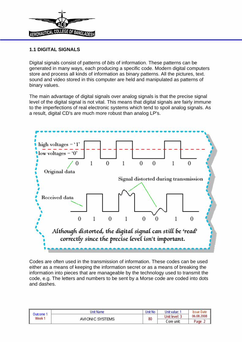
1.1 DIGITAL SIGNALS Digital signals consist of patterns of bits of information. These patterns can be generated in many ways, each producing a specific code. Modern digital computers store and process all kinds of information as binary patterns. All the pictures, text. sound and video stored in this computer are held and manipulated as patterns of binary values. The main advantage of digital signals over analog signals is that the precise signal level of the digital signal is not vital. This means that digital signals are fairly immune to the imperfections of real electronic systems which tend to spoil analog signals. As a result, digital CD's are much more robust than analog LP's.
Codes are often used in the transmission of information. These codes can be used either as a means of keeping the information secret or as a means of breaking the information into pieces that are manageable by the technology used to transmit the code, e.g. The letters and numbers to be sent by a Morse code are coded into dots and dashes.
Unit level: 3 06.08.2008 Issue Date Outcome 1
AVIONIC SYSTEMS Core unit: Week 1 80 Page 3
1.2 COMBINATIONAL LOGIC In digital circuit theory, combinational logic (also called combinatorial logic) is a type of logic circuit whose output is a pure function of the present input only. This is in contrast to sequential logic, in which the output depends not only on the present input but also on the history of the input.
In other words, sequential logic has memory while combinational logic does not.
Combinational logic is used in computer circuits to do Boolean algebra on input signals and on stored data. Practical computer circuits normally contain a mixture of combinational and sequential logic. For example, the part of an arithmetic logic unit, or ALU, that does mathematical calculations is constructed in accord with combinational logic, although the ALU is controlled by a sequencer that is constructed in accord with sequential logic.
1.3 SEQUENTIAL LOGIC
In digital circuit theory, sequential logic is a type of logic circuit whose output depends not only on the present input but also on the history of the input. This is in contrast to combinatorial logic, whose output is a function of, and only of, the present input. In other words, sequential logic has storage (memory) while combinatorial logic does not.
Sequential logic is therefore used to construct some types of computer memory, other types of delay and storage elements, and finite state machines. Most practical computer circuits are a mixture of combinatorial and sequential logic.
There are two types of finite state machine that can be built from sequential logic circuits:
Moore machine: the output depends only on the internal state. (Since the internal state only changes on a clock edge, the output only changes on a clock edge too).
Mealy machine: the output depends not only on the internal state, but also on the inputs.
1.4 MEMORY
Magnetic core memory was popular main memory for computers through the 1960s
Unit Name Unit No Unit value: 1
Unit level: 3 06.08.2008 Issue Date Outcome 1
AVIONIC SYSTEMS Core unit: Week 1 80 Page 4
until it was completely replaced by semiconductor memory.
A computer's memory can be viewed as a list of cells into which numbers can be placed or read. Each cell has a numbered "address" and can store a single number. The computer can be instructed to "put the number 123 into the cell numbered 1357" or to "add the number that is in cell 1357 to the number that is in cell 2468 and put the answer into cell 1595". The information stored in memory may represent practically anything. Letters, numbers, even computer instructions can be placed into memory with equal ease. Since the CPU does not differentiate between different types of information, it is up to the software to give significance to what the memory sees as nothing but a series of numbers.
In almost all modern computers, each memory cell is set up to store binary numbers in groups of eight bits (called a byte). Each byte is able to represent 256 different numbers; either from 0 to 255 or -128 to +127. To store larger numbers, several consecutive bytes may be used (typically, two, four or eight). When negative numbers are required, they are usually stored in two's complement notation. Other arrangements are possible, but are usually not seen outside of specialized applications or historical contexts. A computer can store any kind of information in memory as long as it can be somehow represented in numerical form. Modern computers have billions or even trillions of bytes of memory.
The CPU contains a special set of memory cells called registers that can be read and written to much more rapidly than the main memory area. There are typically between two and one hundred registers depending on the type of CPU. Registers are used for the most frequently needed data items to avoid having to access main memory every time data is needed. Since data is constantly being worked on, reducing the need to access main memory (which is often slow compared to the ALU and control units) greatly increases the computer's speed.
Computer main memory comes in two principal varieties: random access memory or RAM and read-only memory or ROM. RAM can be read and written to anytime the CPU commands it, but ROM is pre-loaded with data and software that never changes, so the CPU can only read from it. ROM is typically used to store the computer's initial start-up instructions. In general, the contents of RAM is erased when the power to the computer is turned off while ROM retains its data indefinitely. In a PC, the ROM contains a specialized program called the BIOS that orchestrates loading the computer's operating system from the hard disk drive into RAM whenever the computer is turned on or reset. In embedded computers, which frequently do not have disk drives, all of the software required to perform the task may be stored in ROM. Software that is stored in ROM is often called firmware because it is notionally more like hardware than software. Flash memory blurs the distinction between ROM and RAM by retaining data when turned off but being rewritable like RAM. However, flash memory is typically much slower than conventional ROM and RAM so its use is restricted to applications where high speeds are not required.
Unit Name Unit No Unit value: 1
Unit level: 3 06.08.2008 Issue Date Outcome 1
AVIONIC SYSTEMS Core unit: Week 1 80 Page 5
In more sophisticated computers there may be one or more RAM cache memories which are slower than registers but faster than main memory. Generally computers with this sort of cache are designed to move frequently needed data into the cache automatically, often without the need for any intervention on the programmer's part.
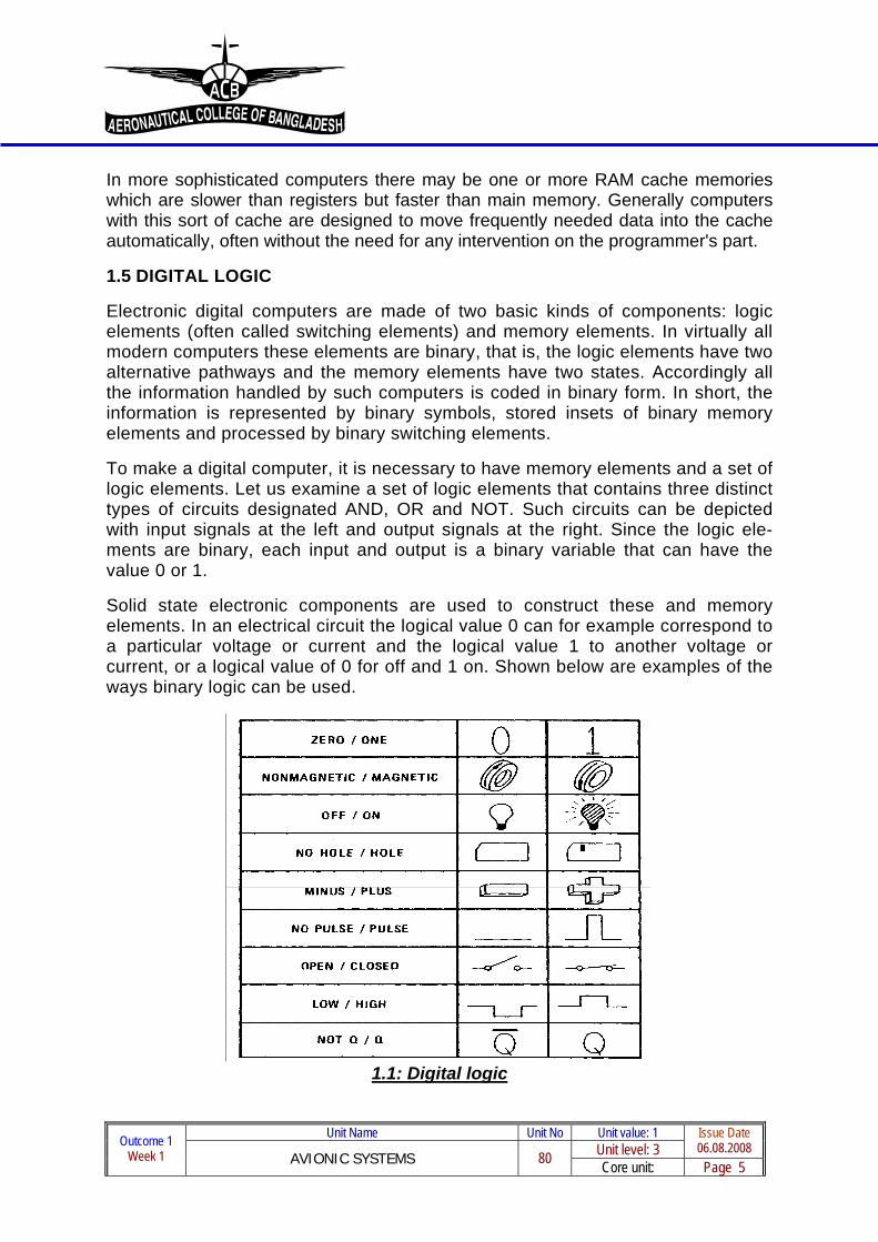
1.5 DIGITAL LOGIC
Electronic digital computers are made of two basic kinds of components: logic elements (often called switching elements) and memory elements. In virtually all modern computers these elements are binary, that is, the logic elements have two alternative pathways and the memory elements have two states. Accordingly all the information handled by such computers is coded in binary form. In short, the information is represented by binary symbols, stored insets of binary memory elements and processed by binary switching elements.
To make a digital computer, it is necessary to have memory elements and a set of logic elements. Let us examine a set of logic elements that contains three distinct types of circuits designated AND, OR and NOT. Such circuits can be depicted with input signals at the left and output signals at the right. Since the logic ele-ments are binary, each input and output is a binary variable that can have the value 0 or 1.
Solid state electronic components are used to construct these and memory elements. In an electrical circuit the logical value 0 can for example correspond to a particular voltage or current and the logical value 1 to another voltage or current, or a logical value of 0 for off and 1 on. Shown below are examples of the ways binary logic can be used.
1.1: Digital logic
Unit Name Unit No Unit value: 1
Unit level: 3 06.08.2008 Issue Date Outcome 1
AVIONIC SYSTEMS Core unit: Week 1 80 Page 6
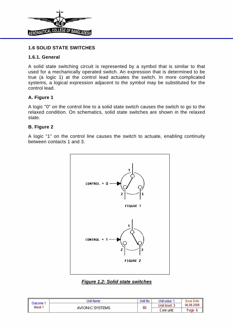
1.6 SOLID STATE SWITCHES
1.6.1. General
A solid state switching circuit is represented by a symbol that is similar to that used for a mechanically operated switch. An expression that is determined to be true (a logic 1) at the control lead actuates the switch. In more complicated systems, a logical expression adjacent to the symbol may be substituted for the control lead.
A. Figure 1
A logic "0" on the control line to a solid state switch causes the switch to go to the relaxed condition. On schematics, solid state switches are shown in the relaxed state.
B. Figure 2
A logic "1" on the control line causes the switch to actuate, enabling continuity between contacts 1 and 3.
Figure 1.2: Solid state switches
Unit Name Unit No Unit value: 1
Unit level: 3 06.08.2008 Issue Date Outcome 1
AVIONIC SYSTEMS Core unit: Week 1 80 Page 7
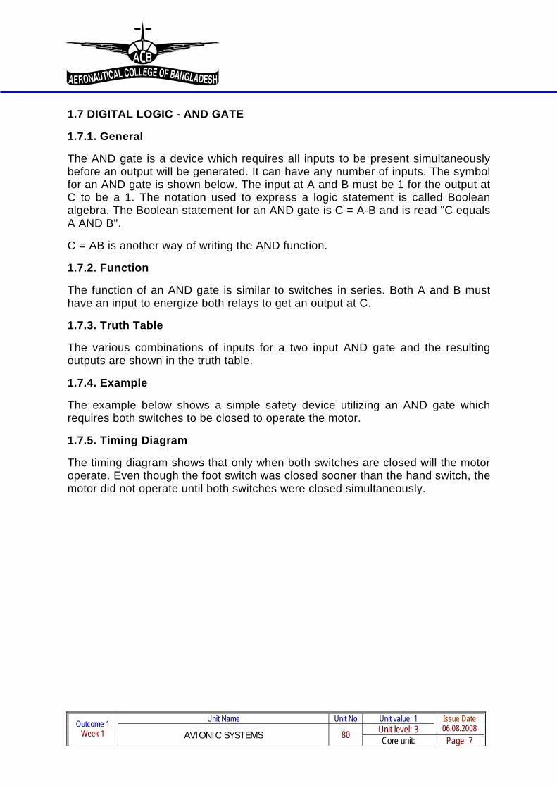
1.7 DIGITAL LOGIC - AND GATE
1.7.1. General
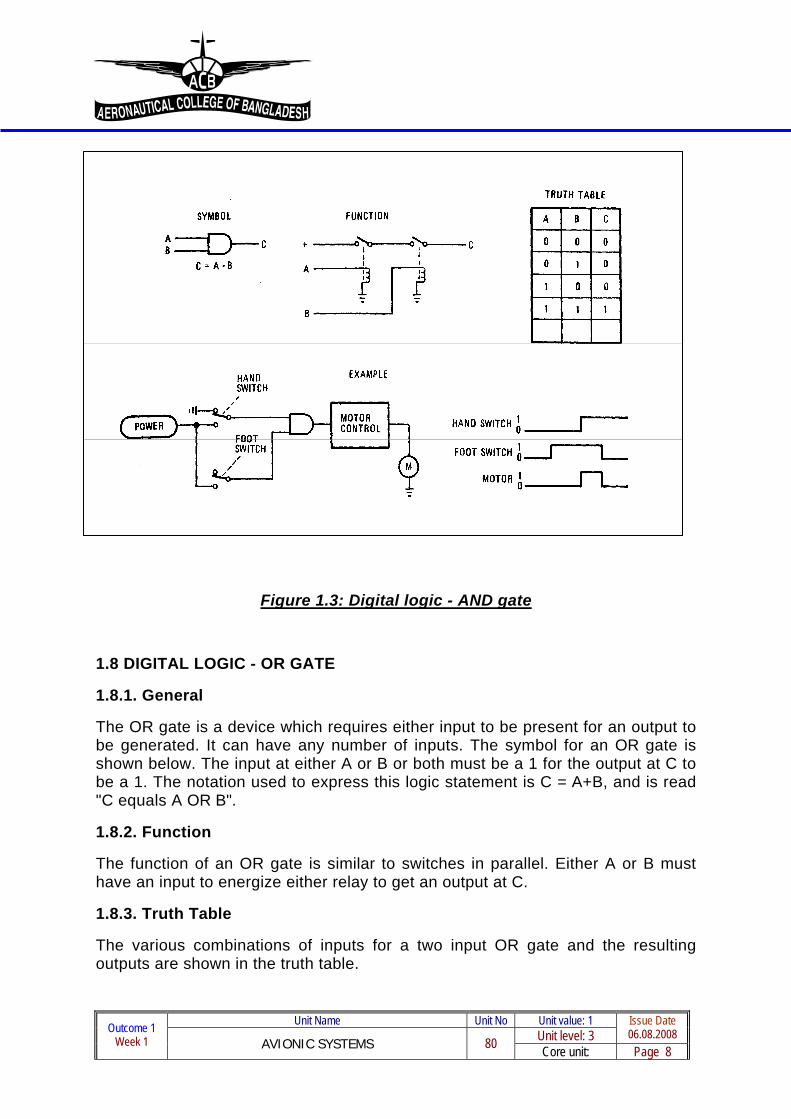
The AND gate is a device which requires all inputs to be present simultaneously before an output will be generated. It can have any number of inputs. The symbol for an AND gate is shown below. The input at A and B must be 1 for the output at C to be a 1. The notation used to express a logic statement is called Boolean algebra. The Boolean statement for an AND gate is C = A-B and is read "C equals A AND B".
C = AB is another way of writing the AND function.
1.7.2. Function
The function of an AND gate is similar to switches in series. Both A and B must have an input to energize both relays to get an output at C.
1.7.3. Truth Table
The various combinations of inputs for a two input AND gate and the resulting outputs are shown in the truth table.
1.7.4. Example
The example below shows a simple safety device utilizing an AND gate which requires both switches to be closed to operate the motor.
1.7.5. Timing Diagram
The timing diagram shows that only when both switches are closed will the motor operate. Even though the foot switch was closed sooner than the hand switch, the motor did not operate until both switches were closed simultaneously.
Unit Name Unit No Unit value: 1
Unit Name Unit No Unit value: 1 Unit level: 3 06.08.2008
Issue Date Outcome 1 AVIONIC SYSTEMS Core unit:
Week 1 80 Page 8
Figure 1.3: Digital logic - AND gate
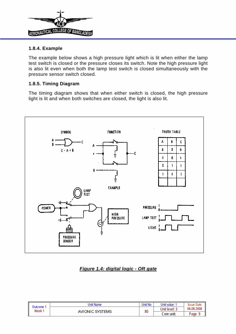
1.8 DIGITAL LOGIC - OR GATE
1.8.1. General
The OR gate is a device which requires either input to be present for an output to be generated. It can have any number of inputs. The symbol for an OR gate is shown below. The input at either A or B or both must be a 1 for the output at C to be a 1. The notation used to express this logic statement is C = A+B, and is read "C equals A OR B".
1.8.2. Function
The function of an OR gate is similar to switches in parallel. Either A or B must have an input to energize either relay to get an output at C.
1.8.3. Truth Table
The various combinations of inputs for a two input OR gate and the resulting outputs are shown in the truth table.
Unit Name Unit No Unit value: 1 Unit level: 3 06.08.2008
Issue Date Outcome 1 AVIONIC SYSTEMS Core unit:
Week 1 80 Page 9
1.8.4. Example
The example below shows a high pressure light which is lit when either the lamp test switch is closed or the pressure closes its switch. Note the high pressure light is also lit even when both the lamp test switch is closed simultaneously with the pressure sensor switch closed.
1.8.5. Timing Diagram
The timing diagram shows that when either switch is closed, the high pressure light is lit and when both switches are closed, the light is also lit.
Figure 1.4: digital logic - OR gate
Unit level: 3 06.08.2008 Issue Date Outcome 1
AVIONIC SYSTEMS Core unit: Week 1 80 Page 10
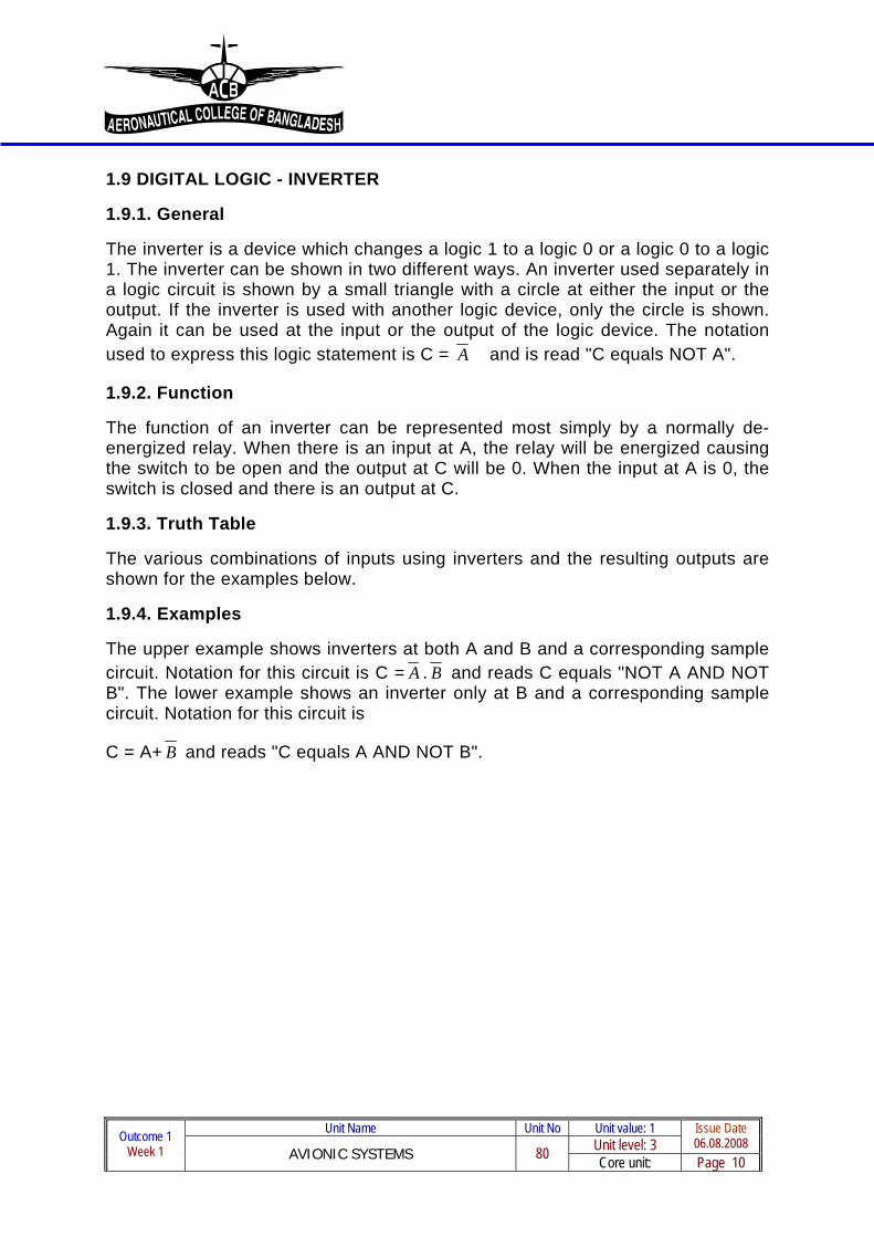
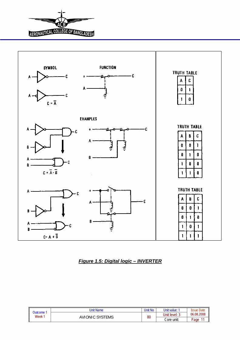
1.9 DIGITAL LOGIC - INVERTER
1.9.1. General
The inverter is a device which changes a logic 1 to a logic 0 or a logic 0 to a logic 1. The inverter can be shown in two different ways. An inverter used separately in a logic circuit is shown by a small triangle with a circle at either the input or the output. If the inverter is used with another logic device, only the circle is shown. Again it can be used at the input or the output of the logic device. The notation used to express this logic statement is C = A and is read "C equals NOT A".
1.9.2. Function
The function of an inverter can be represented most simply by a normally de-energized relay. When there is an input at A, the relay will be energized causing the switch to be open and the output at C will be 0. When the input at A is 0, the switch is closed and there is an output at C.
1.9.3. Truth Table
The various combinations of inputs using inverters and the resulting outputs are shown for the examples below.
1.9.4. Examples
The upper example shows inverters at both A and B and a corresponding sample circuit. Notation for this circuit is C = A . B and reads C equals "NOT A AND NOT B". The lower example shows an inverter only at B and a corresponding sample circuit. Notation for this circuit is
C = A+ B and reads "C equals A AND NOT B".
Unit Name Unit No Unit value: 1
Unit level: 3 06.08.2008 Issue Date Outcome 1
AVIONIC SYSTEMS Core unit: Week 1 80 Page 11
Figure 1.5: Digital logic – INVERTER
Unit Name Unit No Unit value: 1
Unit level: 3 06.08.2008 Issue Date Outcome 1
AVIONIC SYSTEMS Core unit: Week 1 80 Page 12
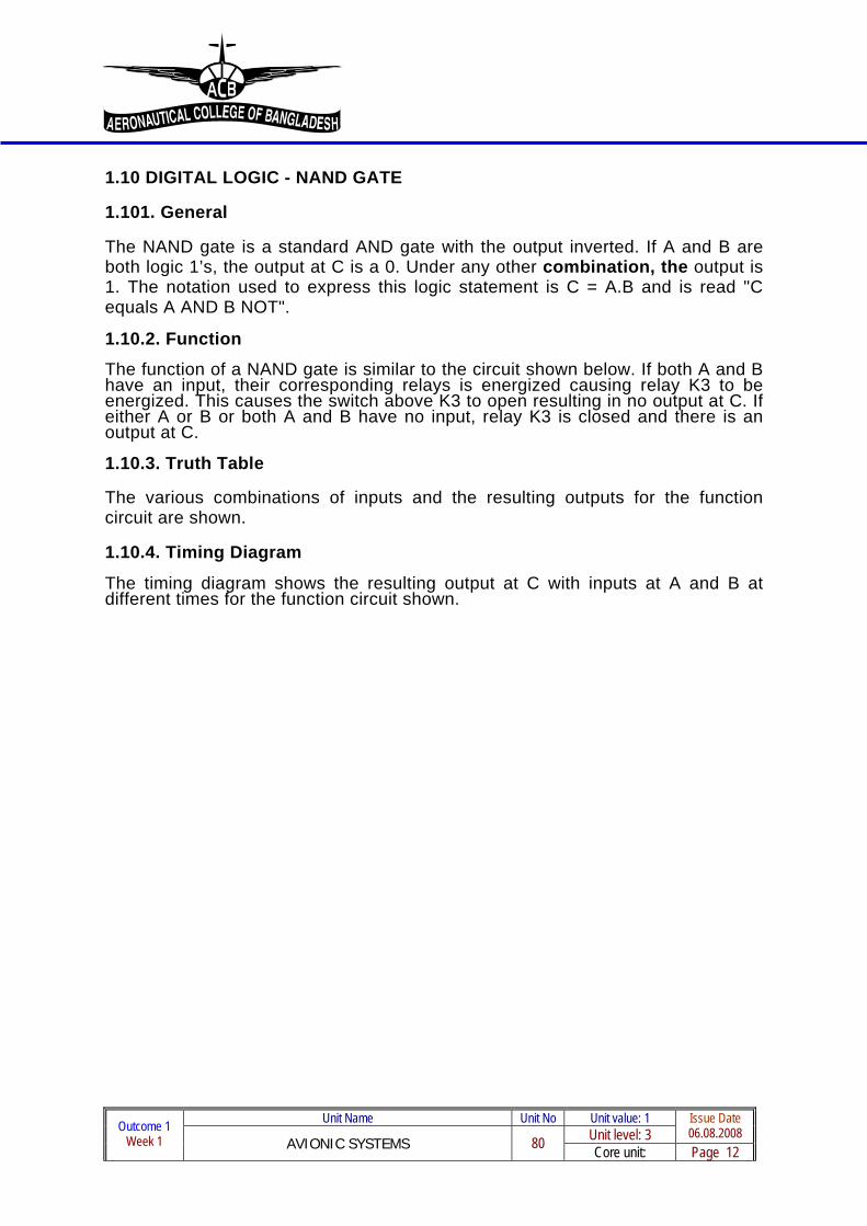
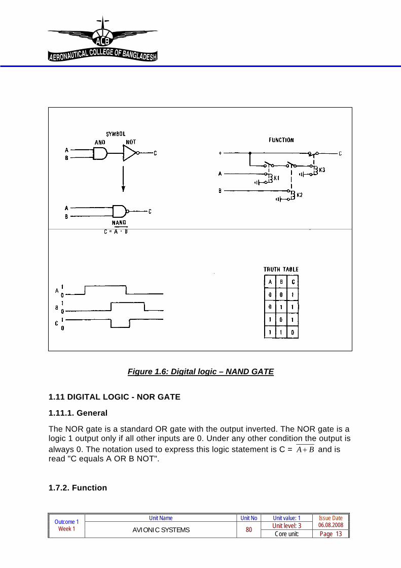
1.10 DIGITAL LOGIC - NAND GATE
1.101. General
The NAND gate is a standard AND gate with the output inverted. If A and B are both logic 1’s, the output at C is a 0. Under any other combination, the output is 1. The notation used to express this logic statement is C = A.B and is read "C equals A AND B NOT".
1.10.2. Function
The function of a NAND gate is similar to the circuit shown below. If both A and B have an input, their corresponding relays is energized causing relay K3 to be energized. This causes the switch above K3 to open resulting in no output at C. If either A or B or both A and B have no input, relay K3 is closed and there is an output at C.
1.10.3. Truth Table
The various combinations of inputs and the resulting outputs for the function circuit are shown.
1.10.4. Timing Diagram
The timing diagram shows the resulting output at C with inputs at A and B at different times for the function circuit shown.
Unit Name Unit No Unit value: 1
Unit level: 3 06.08.2008 Issue Date Outcome 1
AVIONIC SYSTEMS Core unit: Week 1 80 Page 13
Figure 1.6: Digital logic – NAND GATE 1.11 DIGITAL LOGIC - NOR GATE
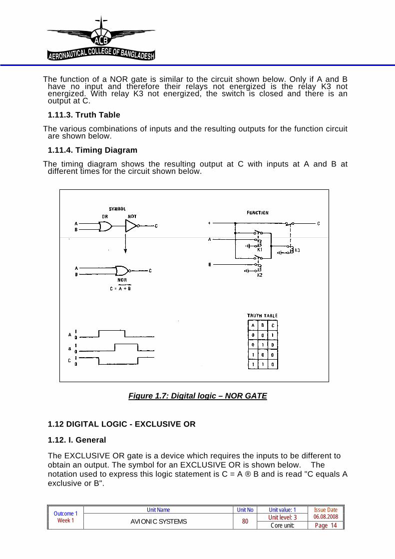
1.11.1. General
The NOR gate is a standard OR gate with the output inverted. The NOR gate is a logic 1 output only if all other inputs are 0. Under any other condition the output is always 0. The notation used to express this logic statement is C = BA+ and is read "C equals A OR B NOT".
1.7.2. Function
Unit Name Unit No Unit value: 1
Unit level: 3 06.08.2008 Issue Date Outcome 1
AVIONIC SYSTEMS Core unit: Week 1 80 Page 14
The function of a NOR gate is similar to the circuit shown below. Only if A and B have no input and therefore their relays not energized is the relay K3 not energized. With relay K3 not energized, the switch is closed and there is an output at C.
1.11.3. Truth Table
The various combinations of inputs and the resulting outputs for the function circuit are shown below.
1.11.4. Timing Diagram
The timing diagram shows the resulting output at C with inputs at A and B at different times for the circuit shown below.
Figure 1.7: Digital logic – NOR GATE
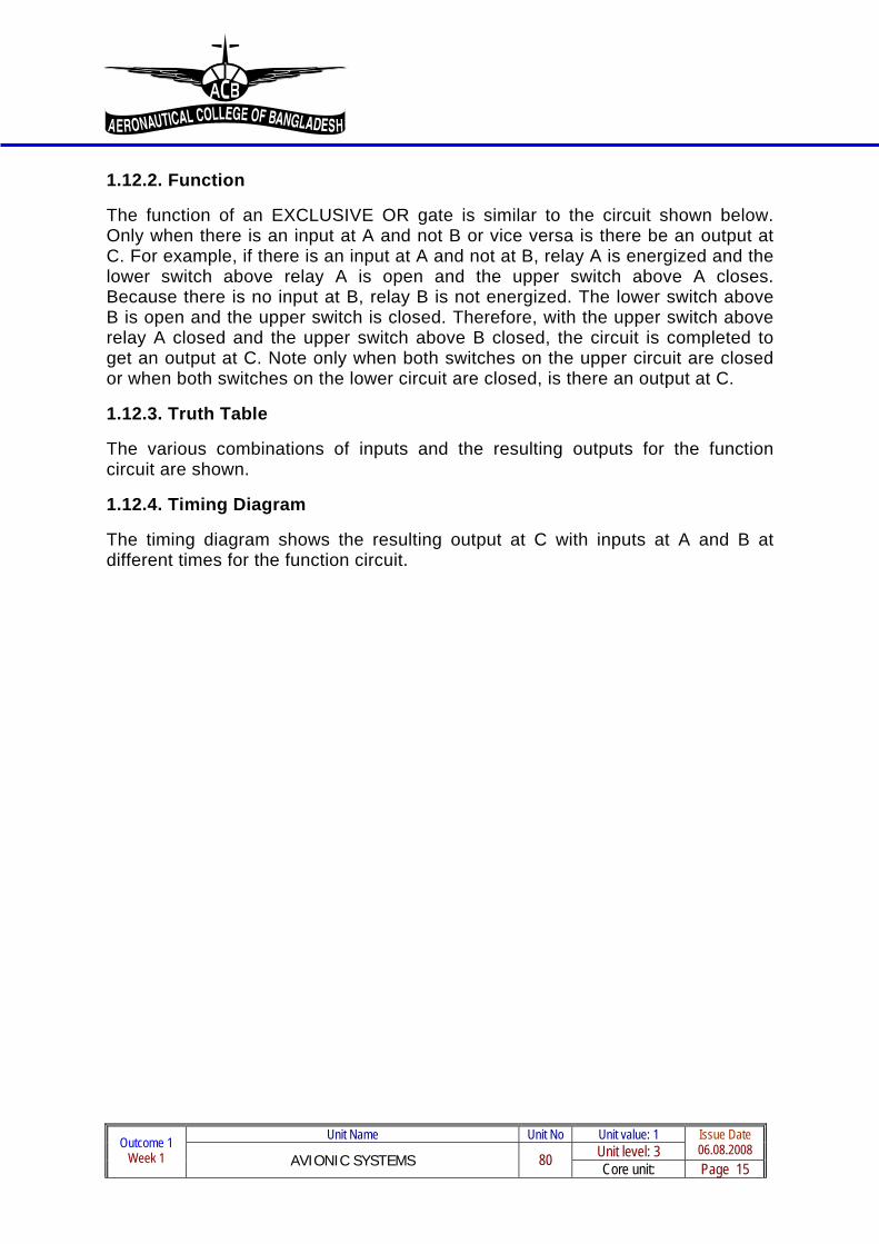
1.12 DIGITAL LOGIC - EXCLUSIVE OR
1.12. I. General
The EXCLUSIVE OR gate is a device which requires the inputs to be different to obtain an output. The symbol for an EXCLUSIVE OR is shown below. The notation used to express this logic statement is C = A ® B and is read "C equals A exclusive or B".
Unit Name Unit No Unit value: 1
Unit level: 3 06.08.2008 Issue Date Outcome 1
AVIONIC SYSTEMS Core unit: Week 1 80 Page 15
1.12.2. Function
The function of an EXCLUSIVE OR gate is similar to the circuit shown below. Only when there is an input at A and not B or vice versa is there be an output at C. For example, if there is an input at A and not at B, relay A is energized and the lower switch above relay A is open and the upper switch above A closes. Because there is no input at B, relay B is not energized. The lower switch above B is open and the upper switch is closed. Therefore, with the upper switch above relay A closed and the upper switch above B closed, the circuit is completed to get an output at C. Note only when both switches on the upper circuit are closed or when both switches on the lower circuit are closed, is there an output at C.
1.12.3. Truth Table
The various combinations of inputs and the resulting outputs for the function circuit are shown.
1.12.4. Timing Diagram
The timing diagram shows the resulting output at C with inputs at A and B at different times for the function circuit.
Unit Name Unit No Unit value: 1
Unit Name Unit No Unit value: 1 Unit level: 3 06.08.2008
Issue Date Outcome 1 AVIONIC SYSTEMS Core unit:
Week 1 80 Page 16
Figure 1.8: Digital logic – EXCLUSIVE OR 1.13 DIGITAL LOGIC - MEMORY DEVICES
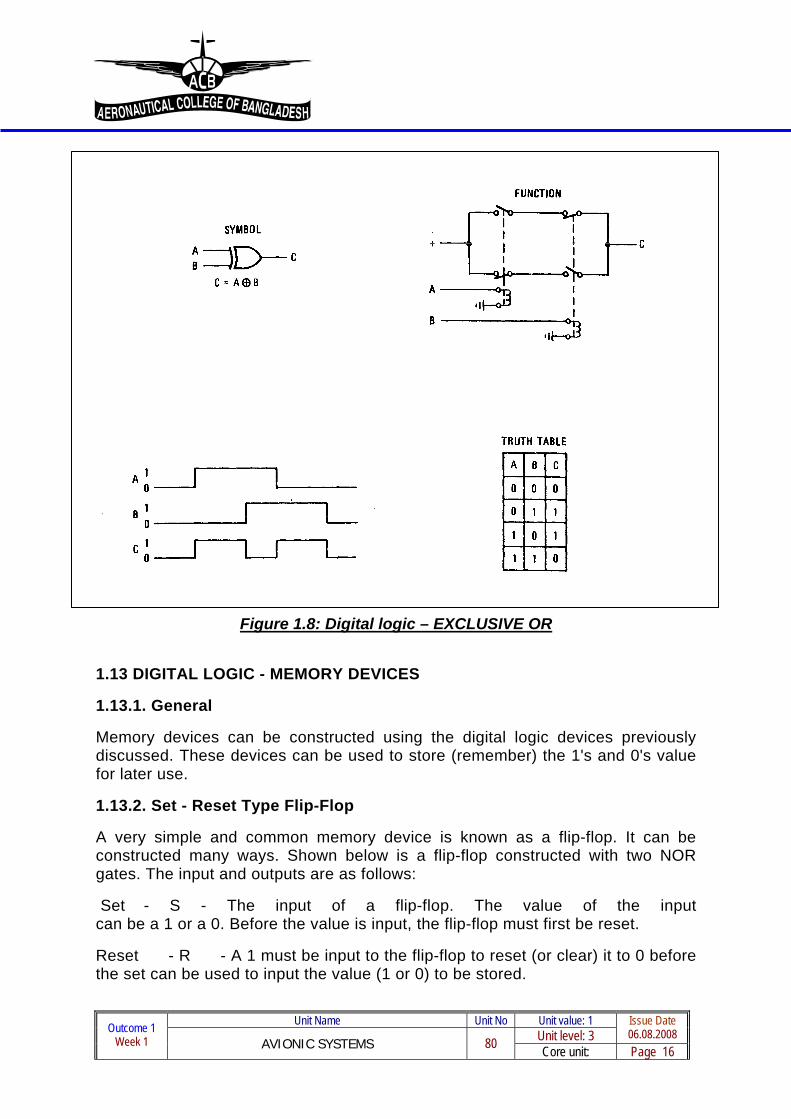
1.13.1. General
Memory devices can be constructed using the digital logic devices previously discussed. These devices can be used to store (remember) the 1's and 0's value for later use.
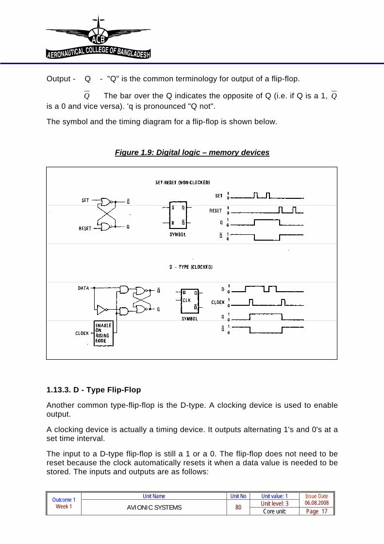
1.13.2. Set - Reset Type Flip-Flop
A very simple and common memory device is known as a flip-flop. It can be constructed many ways. Shown below is a flip-flop constructed with two NOR gates. The input and outputs are as follows:
Set - S - The input of a flip-flop. The value of the input can be a 1 or a 0. Before the value is input, the flip-flop must first be reset.
Reset - R - A 1 must be input to the flip-flop to reset (or clear) it to 0 before the set can be used to input the value (1 or 0) to be stored.
Unit level: 3 06.08.2008 Issue Date Outcome 1
AVIONIC SYSTEMS Core unit: Week 1 80 Page 17
Output - Q - "Q" is the common terminology for output of a flip-flop.
Q The bar over the Q indicates the opposite of Q (i.e. if Q is a 1, Q is a 0 and vice versa). 'q is pronounced "Q not".
The symbol and the timing diagram for a flip-flop is shown below.
Figure 1.9: Digital logic – memory devices
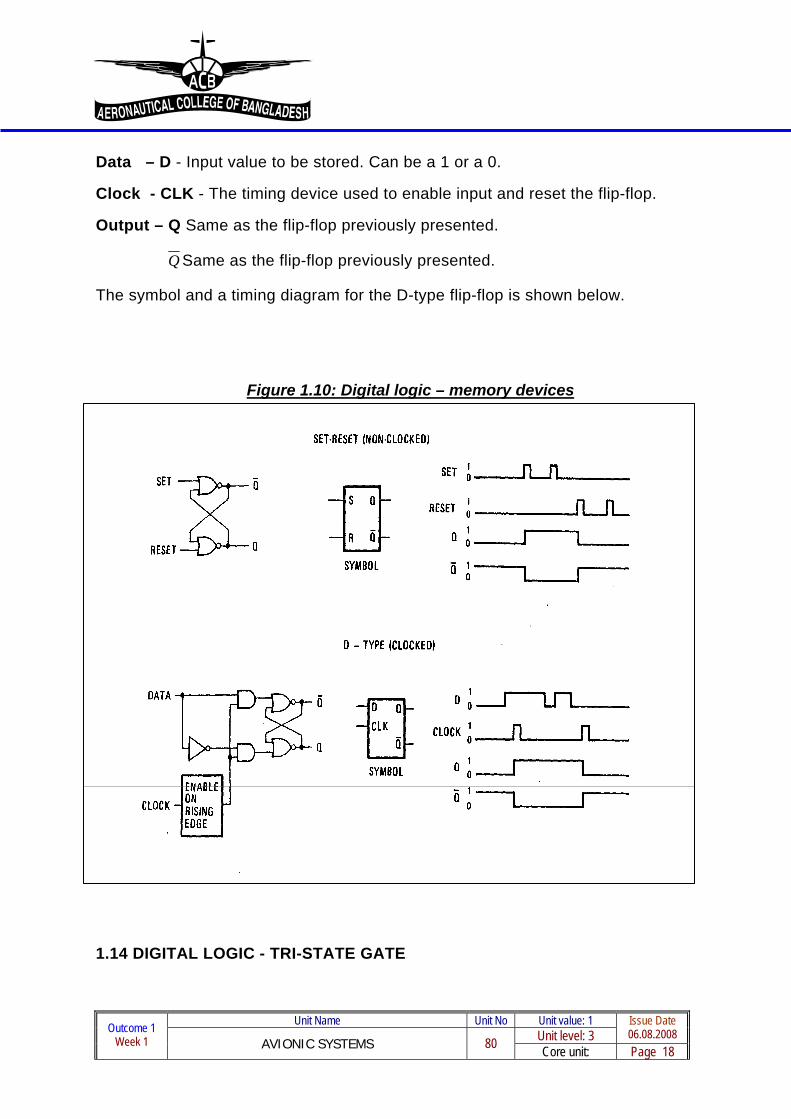
1.13.3. D - Type Flip-Flop
Another common type-flip-flop is the D-type. A clocking device is used to enable output.
A clocking device is actually a timing device. It outputs alternating 1's and 0's at a set time interval.
The input to a D-type flip-flop is still a 1 or a 0. The flip-flop does not need to be reset because the clock automatically resets it when a data value is needed to be stored. The inputs and outputs are as follows:
Unit Name Unit No Unit value: 1
Unit level: 3 06.08.2008 Issue Date Outcome 1
AVIONIC SYSTEMS Core unit: Week 1 80 Page 18
Data – D - Input value to be stored. Can be a 1 or a 0.
Clock - CLK - The timing device used to enable input and reset the flip-flop.
Output – Q Same as the flip-flop previously presented.
Q Same as the flip-flop previously presented.
The symbol and a timing diagram for the D-type flip-flop is shown below.
Figure 1.10: Digital logic – memory devices
1.14 DIGITAL LOGIC - TRI-STATE GATE
Unit Name Unit No Unit value: 1
Unit level: 3 06.08.2008 Issue Date Outcome 1
AVIONIC SYSTEMS Core unit: Week 1 80 Page 19
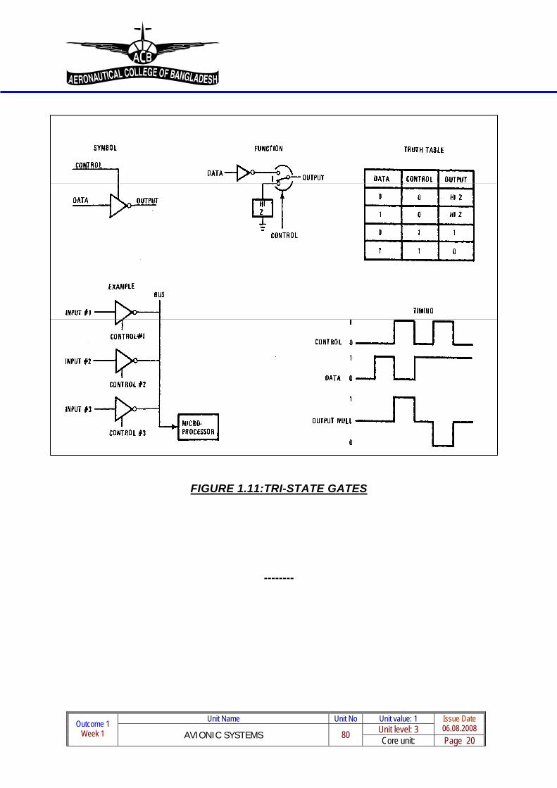
1.14.1 General
Tri-state gates are designed so that the output exhibits three distinct states. It may act as a normal gate with a low-impedance logic 1 and logic 0 when the control input is enabled. A third state, having very high output impedance occurs when the control input is disabled.
1.14.2 Function
The function of a tri-state gate is similar to a switch with one input tied to high impedance, the other to the output of an inverter.
1.14.3 Truth Table
The various combinations of data and control and the resulting outputs are shown in the truth table.
1.14.4 Example
In the exam le below, tri-state control is used to allow more than one device to snare a common bus, but not at the same time.
1.14.5 Timing Diagram
The timing diagram shows that when the control is disabled (0) the output is at a null (high impedance); when the control is enabled (1) the input data is inverted and appears at the output.
Unit Name Unit No Unit value: 1
Unit Name Unit No Unit value: 1 Unit level: 3 06.08.2008
Issue Date Outcome 1 AVIONIC SYSTEMS Core unit:
Week 1 80 Page 20
FIGURE 1.11:TRI-STATE GATES
--------
Related Documents