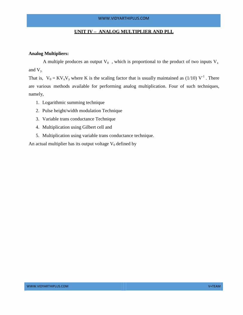
WWW.VIDYARTHIPLUS.COM WWW.VIDYARTHIPLUS.COM V+TEAM UNIT IV – ANALOG MULTIPLIER AND PLL Analog Multipliers: A multiple produces an output V 0 , which is proportional to the product of two inputs V x and V y. That is, V 0 = KV x V y where K is the scaling factor that is usually maintained as (1/10) V -1 . There are various methods available for performing analog multiplication. Four of such techniques, namely, 1. Logarithmic summing technique 2. Pulse height/width modulation Technique 3. Variable trans conductance Technique 4. Multiplication using Gilbert cell and 5. Multiplication using variable trans conductance technique. An actual multiplier has its output voltage V 0 defined by

Welcome message from author
This document is posted to help you gain knowledge. Please leave a comment to let me know what you think about it! Share it to your friends and learn new things together.
Transcript
WWW.VIDYARTHIPLUS.COM
WWW.VIDYARTHIPLUS.COM V+TEAM
UNIT IV – ANALOG MULTIPLIER AND PLL
Analog Multipliers:
A multiple produces an output V0 , which is proportional to the product of two inputs Vx
and Vy.
That is, V0 = KVxVy where K is the scaling factor that is usually maintained as (1/10) V-1
. There
are various methods available for performing analog multiplication. Four of such techniques,
namely,
1. Logarithmic summing technique
2. Pulse height/width modulation Technique
3. Variable trans conductance Technique
4. Multiplication using Gilbert cell and
5. Multiplication using variable trans conductance technique.
An actual multiplier has its output voltage V0 defined by
WWW.VIDYARTHIPLUS.COM
WWW.VIDYARTHIPLUS.COM V+TEAM
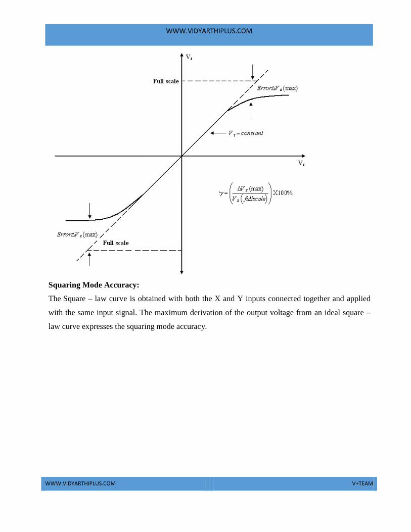
Squaring Mode Accuracy:
The Square – law curve is obtained with both the X and Y inputs connected together and applied
with the same input signal. The maximum derivation of the output voltage from an ideal square –
law curve expresses the squaring mode accuracy.
WWW.VIDYARTHIPLUS.COM
WWW.VIDYARTHIPLUS.COM V+TEAM
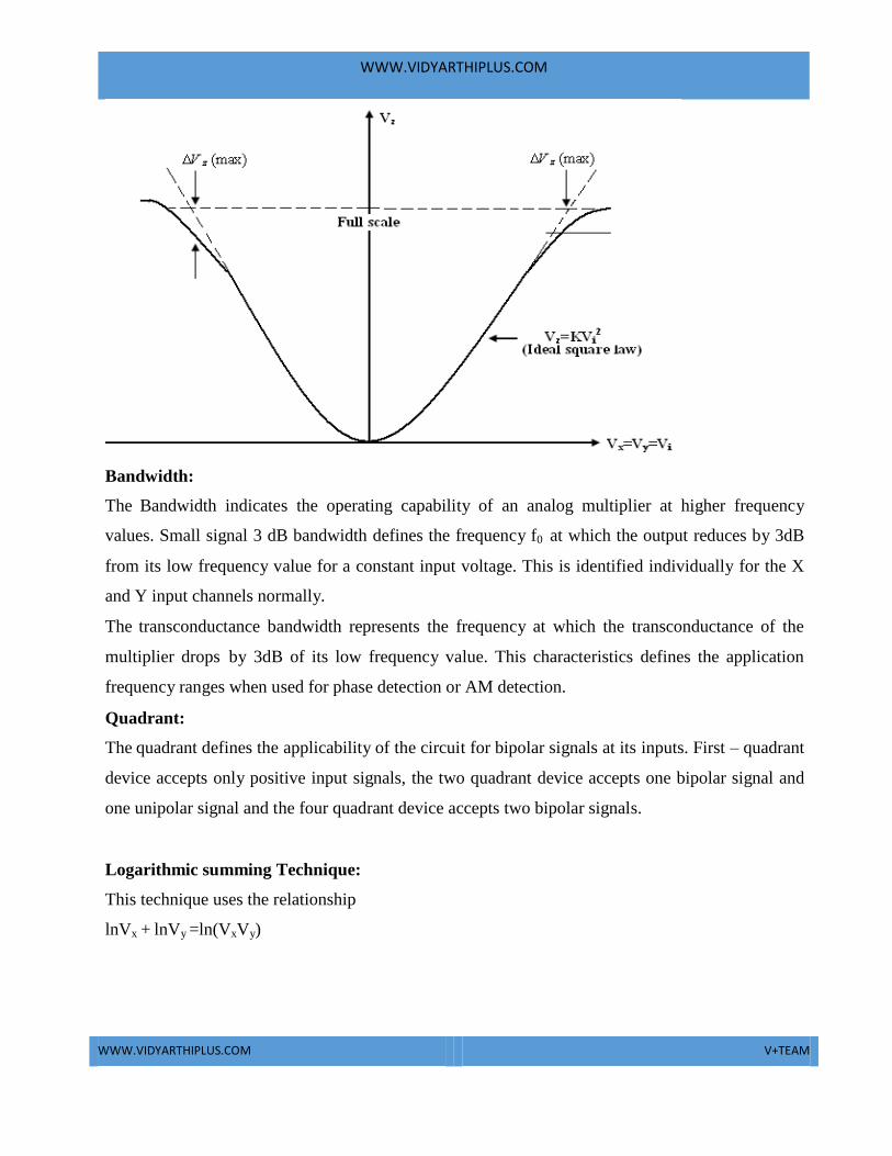
Bandwidth:
The Bandwidth indicates the operating capability of an analog multiplier at higher frequency
values. Small signal 3 dB bandwidth defines the frequency f0 at which the output reduces by 3dB
from its low frequency value for a constant input voltage. This is identified individually for the X
and Y input channels normally.
The transconductance bandwidth represents the frequency at which the transconductance of the
multiplier drops by 3dB of its low frequency value. This characteristics defines the application
frequency ranges when used for phase detection or AM detection.
Quadrant:
The quadrant defines the applicability of the circuit for bipolar signals at its inputs. First – quadrant
device accepts only positive input signals, the two quadrant device accepts one bipolar signal and
one unipolar signal and the four quadrant device accepts two bipolar signals.
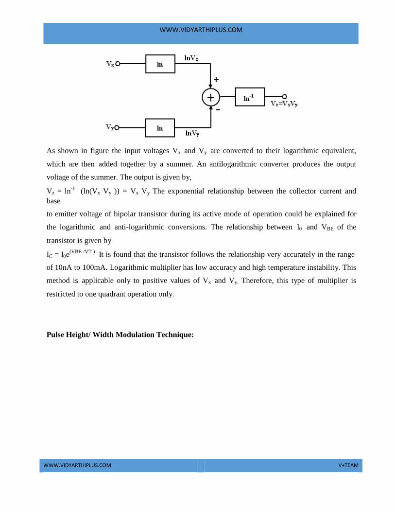
Logarithmic summing Technique:
This technique uses the relationship
lnVx + lnVy =ln(VxVy)
WWW.VIDYARTHIPLUS.COM
WWW.VIDYARTHIPLUS.COM V+TEAM
As shown in figure the input voltages Vx and Vy are converted to their logarithmic equivalent,
which are then added together by a summer. An antilogarithmic converter produces the output
voltage of the summer. The output is given by,
Vz = ln-1
(ln(Vx Vy )) = Vx Vy The exponential relationship between the collector current and
base
to emitter voltage of bipolar transistor during its active mode of operation could be explained for
the logarithmic and anti-logarithmic conversions. The relationship between I0 and VBE of the
transistor is given by
IC = I0e(VBE /VT )
It is found that the transistor follows the relationship very accurately in the range
of 10nA to 100mA. Logarithmic multiplier has low accuracy and high temperature instability. This
method is applicable only to positive values of Vx and Vy. Therefore, this type of multiplier is
restricted to one quadrant operation only.
Pulse Height/ Width Modulation Technique:
WWW.VIDYARTHIPLUS.COM
WWW.VIDYARTHIPLUS.COM V+TEAM
K
In this method, the pulse width of a pulse train is made proportional to one input voltage and the
pulse amplitude is made proportional to the second input voltage. Therefore, Vx =Kx A, Vy =Ky t,
and Vz =Kz T where Kx , Ky , Kz are scaling factors. In figure A is the amplitude of the pulse, t is the
pulse width and T is the area of the pulse. Therefore,
The modulated pulse train is passed through an integrated circuit. Therefore, the input of the
integrator is proportional to the area of pulse, which in turn is proportional to the product of two
input voltages.
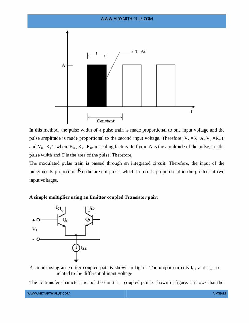
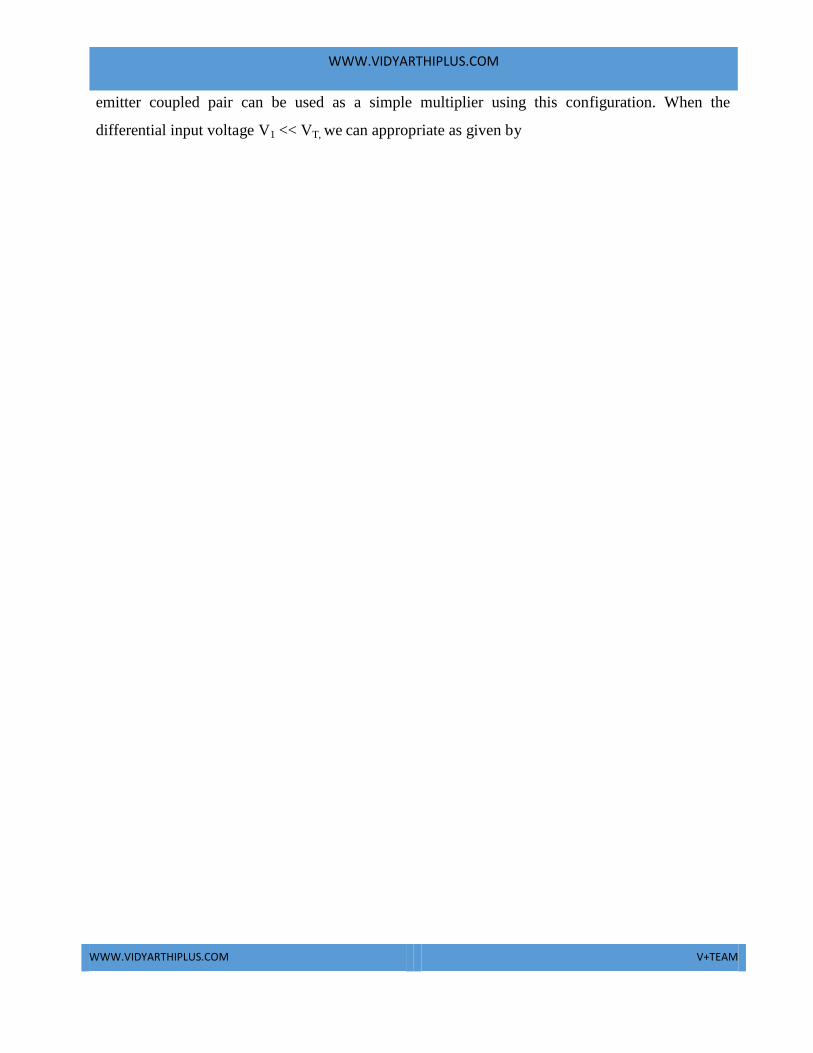
A simple multiplier using an Emitter coupled Transistor pair:
A circuit using an emitter coupled pair is shown in figure. The output currents IC1 and IC2 are related to the differential input voltage
The dc transfer characteristics of the emitter – coupled pair is shown in figure. It shows that the
WWW.VIDYARTHIPLUS.COM
WWW.VIDYARTHIPLUS.COM V+TEAM
emitter coupled pair can be used as a simple multiplier using this configuration. When the
differential input voltage V1 << VT, we can appropriate as given by
WWW.VIDYARTHIPLUS.COM
WWW.VIDYARTHIPLUS.COM V+TEAM
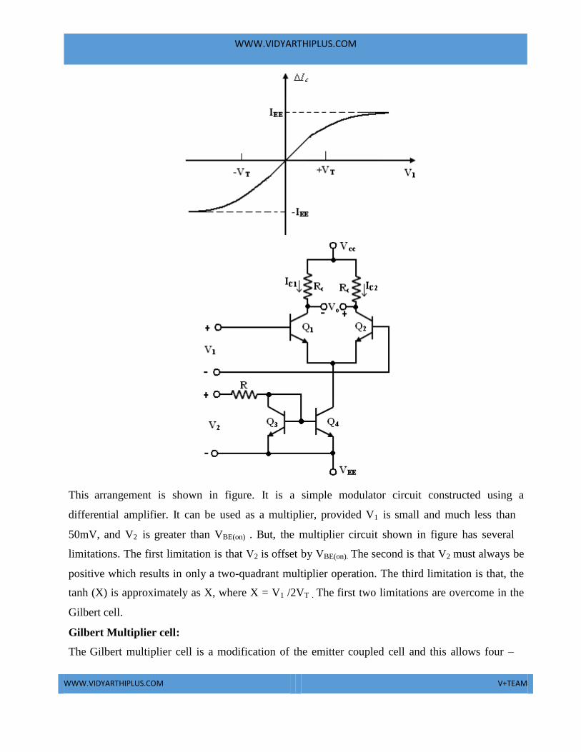
This arrangement is shown in figure. It is a simple modulator circuit constructed using a
differential amplifier. It can be used as a multiplier, provided V1 is small and much less than
50mV, and V2 is greater than VBE(on) . But, the multiplier circuit shown in figure has several
limitations. The first limitation is that V2 is offset by VBE(on). The second is that V2 must always be
positive which results in only a two-quadrant multiplier operation. The third limitation is that, the
tanh (X) is approximately as X, where X = V1 /2VT . The first two limitations are overcome in the
Gilbert cell.
Gilbert Multiplier cell:
The Gilbert multiplier cell is a modification of the emitter coupled cell and this allows four –

WWW.VIDYARTHIPLUS.COM
WWW.VIDYARTHIPLUS.COM V+TEAM
quadrant multiplication. Therefore, it forms the basis of most of the integrated circuit balanced
WWW.VIDYARTHIPLUS.COM
WWW.VIDYARTHIPLUS.COM V+TEAM
multipliers. Two cross- coupled emitter- coupled pairs in series connection with an emitter coupled
pair form the structure of the Gilbert multiplier cell.
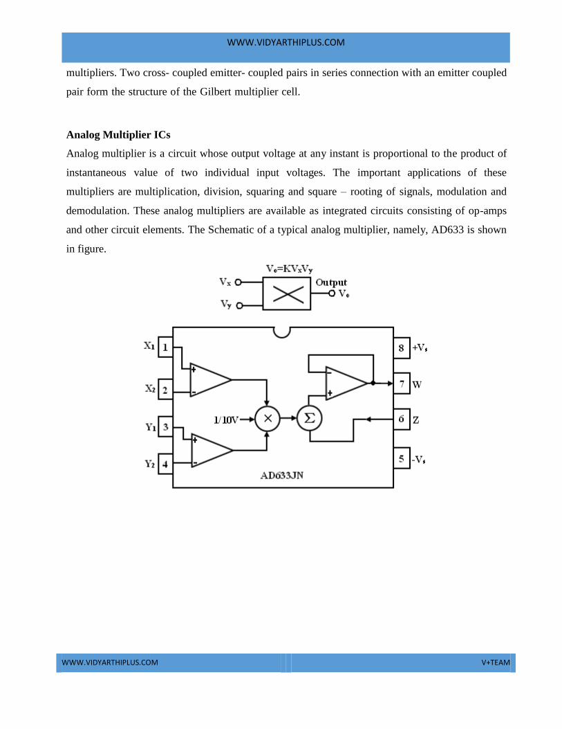
Analog Multiplier ICs
Analog multiplier is a circuit whose output voltage at any instant is proportional to the product of
instantaneous value of two individual input voltages. The important applications of these
multipliers are multiplication, division, squaring and square – rooting of signals, modulation and
demodulation. These analog multipliers are available as integrated circuits consisting of op-amps
and other circuit elements. The Schematic of a typical analog multiplier, namely, AD633 is shown
in figure.
WWW.VIDYARTHIPLUS.COM
WWW.VIDYARTHIPLUS.COM V+TEAM
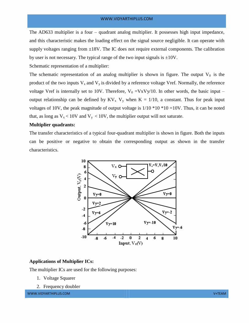
The AD633 multiplier is a four – quadrant analog multiplier. It possesses high input impedance,
and this characteristic makes the loading effect on the signal source negligible. It can operate with
supply voltages ranging from ±18V. The IC does not require external components. The calibration
by user is not necessary. The typical range of the two input signals is ±10V.
Schematic representation of a multiplier:
The schematic representation of an analog multiplier is shown in figure. The output V0 is the
product of the two inputs Vx and Vy is divided by a reference voltage Vref. Normally, the reference
voltage Vref is internally set to 10V. Therefore, V0 =VxVy/10. In other words, the basic input –
output relationship can be defined by KVx Vy when K = 1/10, a constant. Thus for peak input
voltages of 10V, the peak magnitude of output voltage is 1/10 *10 *10 =10V. Thus, it can be noted
that, as long as Vx < 10V and Vy < 10V, the multiplier output will not saturate.
Multiplier quadrants:
The transfer characteristics of a typical four-quadrant multiplier is shown in figure. Both the inputs
can be positive or negative to obtain the corresponding output as shown in the transfer
characteristics.
Applications of Multiplier ICs:
The multiplier ICs are used for the following purposes:
1. Voltage Squarer
2. Frequency doubler
WWW.VIDYARTHIPLUS.COM
WWW.VIDYARTHIPLUS.COM V+TEAM
A
3. Voltage divider
4. Square rooter
5. Phase angle detector
6. Rectifier
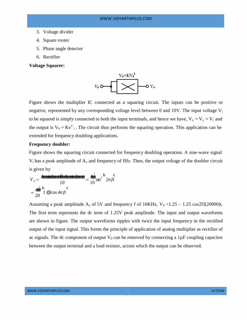
Voltage Squarer:
Figure shows the multiplier IC connected as a squaring circuit. The inputs can be positive or
negative, represented by any corresponding voltage level between 0 and 10V. The input voltage Vi
to be squared is simply connected to both the input terminals, and hence we have, Vx = Vy = Vi and
the output is V0 = Kv2
i . The circuit thus performs the squaring operation. This application can be
extended for frequency doubling applications.
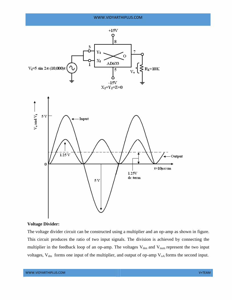
Frequency doubler:
Figure shows the squaring circuit connected for frequency doubling operation. A sine-wave signal
Vi has a peak amplitude of Av and frequency of fHz. Then, the output voltage of the doubler circuit
is given by 2 b c
V 0 Affffvffffsfffiffnfff2fffffffffffftfffBffffffffAfffffvffffsfffifnfffff2fffffffffffftfff
10
Affffvffffsin
2 2ft
10 2 b c
ffffvffff
1 @cos 4 ft 20
Assuming a peak amplitude Av of 5V and frequency f of 10KHz, V0 =1.25 – 1.25 cos2Π(20000)t.
The first term represents the dc term of 1.25V peak amplitude. The input and output waveforms
are shown in figure. The output waveforms ripples with twice the input frequency in the rectified
output of the input signal. This forms the principle of application of analog multiplier as rectifier of
ac signals. The dc component of output V0 can be removed by connecting a 1µF coupling capacitor
between the output terminal and a load resistor, across which the output can be observed.
WWW.VIDYARTHIPLUS.COM
WWW.VIDYARTHIPLUS.COM V+TEAM
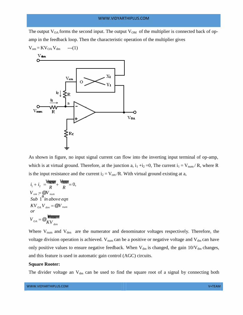
Voltage Divider:
The voltage divider circuit can be constructed using a multiplier and an op-amp as shown in figure.
This circuit produces the ratio of two input signals. The division is achieved by connecting the
multiplier in the feedback loop of an op-amp. The voltages Vden and Vnum represent the two input
voltages, Vdm forms one input of the multiplier, and output of op-amp VoA forms the second input.
WWW.VIDYARTHIPLUS.COM
WWW.VIDYARTHIPLUS.COM V+TEAM
The output VOA forms the second input. The output VOM of the multiplier is connected back of op-
amp in the feedback loop. Then the characteristic operation of the multiplier gives
Vom = KVOA Vdm ---(1)
As shown in figure, no input signal current can flow into the inverting input terminal of op-amp,
which is at virtual ground. Therefore, at the junction a, i1 +i2 =0, The current i1 = Vnum / R, where R
is the input resistance and the current i2 = Vom /R. With virtual ground existing at a,
i1 i2 Vffffnffufffmfffff
R
Vffffofffmfffff R
0,
V om @V num
` a Sub 1 in above eqn
KV OA V den @V num
or
V OA
@ Vffffffnfffuffmffffffff KV
den
Where Vnum and Vden are the numerator and denominator voltages respectively. Therefore, the
voltage division operation is achieved. Vnum can be a positive or negative voltage and Vdm can have
only positive values to ensure negative feedback. When Vdm is changed, the gain 10/Vdm changes,
and this feature is used in automatic gain control (AGC) circuits.
Square Rooter:
The divider voltage an Vdm can be used to find the square root of a signal by connecting both

WWW.VIDYARTHIPLUS.COM
WWW.VIDYARTHIPLUS.COM V+TEAM
inputs of the multiplier to the output of the op-amp. Then, the output voltage of the multiplier VOM
WWW.VIDYARTHIPLUS.COM
WWW.VIDYARTHIPLUS.COM V+TEAM
` a
is equal in magnitude but opposite in polarity (with respect to ground) to Vi. But we know that Vom
is one- term (Scale factor) of V0 * V0 or
-Vi = Vom = V2
0
Solving for V0 and eliminating √-1 yields.
V0 = √10|Vi |
Eqn states that V0 equals the square root of 10 times the absolute magnitude of Vi . The input
voltage Vi must be negative, or else, the op-amp saturates. The range of Vi is between -1 and -10V.
Voltages less than -1V will cause inaccuracies in the result. The diode prevents negative saturation
for positive polarity Vi signals. For positive values of Vi the diode connections are reversed.
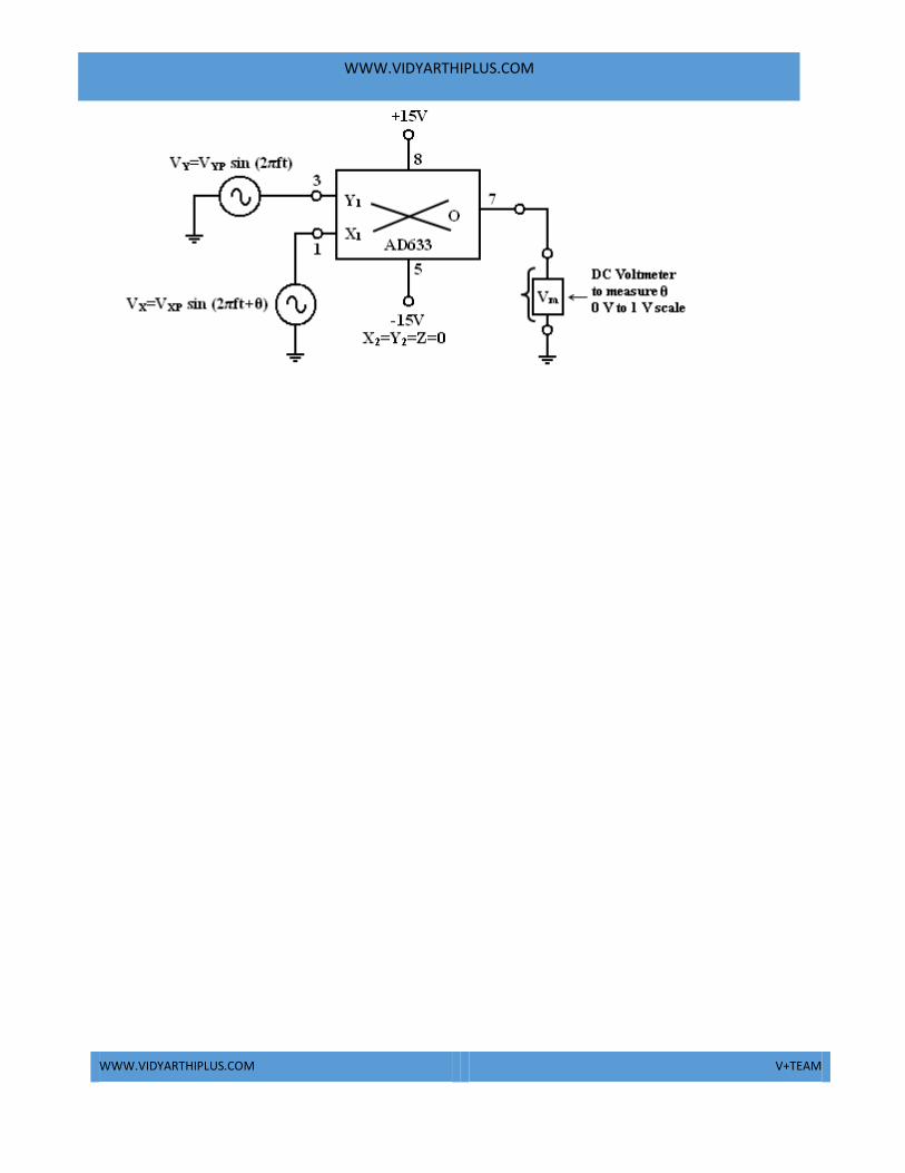
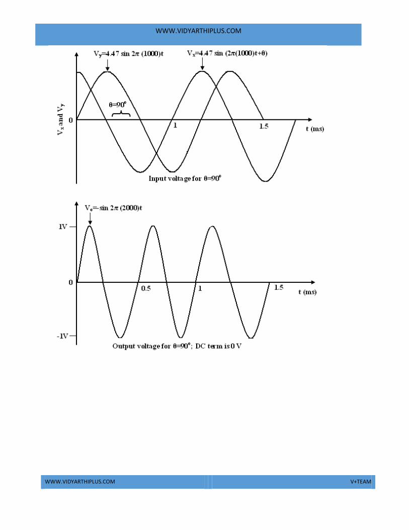
Phase Angle detector:
The multiplier configured for phase angle detection measurement is shown in figure. When two
sine-waves of the same frequency are applied to the inputs of the multiplier, the output V0 has a dc
component and an ac component.
The trigonometric identity shows that
Sin A sin B =1/2 (cos(A-B) – cos(A+B)).
When the two frequencies are equal, but with different phase angles, e.g. A=2πft +ζ for signal Vx
amd B= 2πft for signal Vy, , then using the identity D b cEDb cE D
b cE
sin 2ft
b
sin2ft 1fff
cos @cos 4ft 2
1fff
dc the double frequency term 2
Therefore, when the two input signals Vx and Vy are applied to the multiplier, V0(dc) is given by
a VfffxffpfffVfffffyffpfff
cos
V 0 `
dc 20
where Vxp and Vyp are the peak voltage amplitudes of the signals Vx and Vy. Thus, the output V0(dc)
depends on the factor cos ζ. A dc voltmeter can be calibrated as a phase angle meter when the
product of Vxp and Vyp is made equal to 20. Then, a (0-1) V range dc voltmeter can directly read
cos ζ, with the meter calibrated directly in degrees from a cosine table. The input and output
waveforms are shown in figure.
Then the above eqn becomes V0(dc) = cos ζ, if we make the product Vxp Vyp = 20 or in other words,
Vxp – Vyp = 4.47V
WWW.VIDYARTHIPLUS.COM
WWW.VIDYARTHIPLUS.COM V+TEAM
WWW.VIDYARTHIPLUS.COM
WWW.VIDYARTHIPLUS.COM V+TEAM
WWW.VIDYARTHIPLUS.COM
WWW.VIDYARTHIPLUS.COM V+TEAM
PHASE LOCKED LOOP:
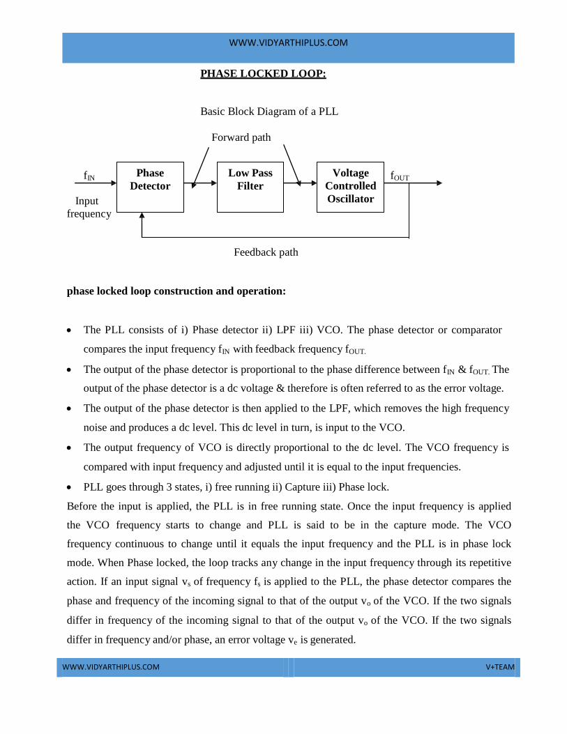
Basic Block Diagram of a PLL
Forward path
fIN
Input
frequency
Phase
Detector
Low Pass
Filter
Voltage
Controlled
Oscillator
fOUT
Feedback path
phase locked loop construction and operation:
The PLL consists of i) Phase detector ii) LPF iii) VCO. The phase detector or comparator
compares the input frequency fIN with feedback frequency fOUT.
The output of the phase detector is proportional to the phase difference between fIN & fOUT. The
output of the phase detector is a dc voltage & therefore is often referred to as the error voltage.
The output of the phase detector is then applied to the LPF, which removes the high frequency
noise and produces a dc level. This dc level in turn, is input to the VCO.
The output frequency of VCO is directly proportional to the dc level. The VCO frequency is
compared with input frequency and adjusted until it is equal to the input frequencies.
PLL goes through 3 states, i) free running ii) Capture iii) Phase lock.
Before the input is applied, the PLL is in free running state. Once the input frequency is applied
the VCO frequency starts to change and PLL is said to be in the capture mode. The VCO
frequency continuous to change until it equals the input frequency and the PLL is in phase lock
mode. When Phase locked, the loop tracks any change in the input frequency through its repetitive
action. If an input signal vs of frequency fs is applied to the PLL, the phase detector compares the
phase and frequency of the incoming signal to that of the output vo of the VCO. If the two signals
differ in frequency of the incoming signal to that of the output vo of the VCO. If the two signals
differ in frequency and/or phase, an error voltage ve is generated.
WWW.VIDYARTHIPLUS.COM
WWW.VIDYARTHIPLUS.COM V+TEAM
The phase detector is basically a multiplier and produces the sum (fs + fo) and difference (fs - fo)
components at its output. The high frequency component (fs + fo) is removed by the low pass filter
and the difference frequency component is amplified then applied as control voltage vc to VCO.
The signal vc shifts the VCO frequency in a direction to reduce the frequency difference between fs
and fo. Once this action starts, we say that the signal is in the capture range. The VCO continues to
change frequency till its output frequency is exactly the same as the input signal frequency. The
circuit is then said to be locked. Once locked, the output frequency fo of VCO is identical to fs
except for a finite phase difference φ. This phase difference φ generates a corrective control
voltage vc to shift the VCO frequency from f0 to fs and thereby maintain the lock. Once
locked, PLL tracks the frequency changes of the input signal. Thus, a PLL goes through three
stages (i) free running, (ii) capture and (iii) locked or tracking.
Capture range: the range of frequencies over which the PLL can acquire lock with an input signal
is called the capture range. This parameter is also expressed as percentage of fo.
Pull-in time: the total time taken by the PLL to establish lock is called pull-in time. This depends
on the initial phase and frequency difference between the two signals as well as on the overall loop
gain and loop filter characteristics.
(a) Phase Detector:
Phase detector compares the input frequency and VCO frequency and generates DC voltage
i.e., proportional to the phase difference between the two frequencies. Depending on whether the
analog/digital phase detector is used, the PLL is called either an analog/digital type respectively.
Even though most monolithic PLL integrated circuits use analog phase detectors.
Ex for Analog: Double-balanced mixer
Ex for Digital: Ex-OR, Edge trigger, monolithic Phase detector.
Ex-OR Phase Detector:
This uses an exclusive OR gate. The output of the Ex-OR gate is high only when fIN or fOUT is
high.
The DC output voltage of the Ex-OR phase detector is a function of the phase difference between
its two outputs. The maximum dc output voltage occurs when the phase difference is Π radians or
WWW.VIDYARTHIPLUS.COM
WWW.VIDYARTHIPLUS.COM V+TEAM
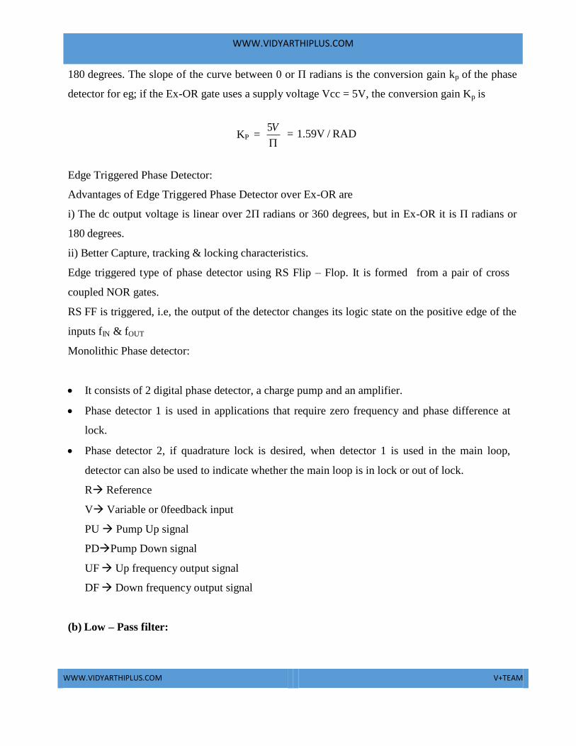
180 degrees. The slope of the curve between 0 or Π radians is the conversion gain kp of the phase
detector for eg; if the Ex-OR gate uses a supply voltage Vcc = 5V, the conversion gain Kp is
5V KP =
= 1.59V / RAD
Edge Triggered Phase Detector:
Advantages of Edge Triggered Phase Detector over Ex-OR are
i) The dc output voltage is linear over 2Π radians or 360 degrees, but in Ex-OR it is Π radians or
180 degrees.
ii) Better Capture, tracking & locking characteristics.
Edge triggered type of phase detector using RS Flip – Flop. It is formed from a pair of cross
coupled NOR gates.
RS FF is triggered, i.e, the output of the detector changes its logic state on the positive edge of the
inputs fIN & fOUT
Monolithic Phase detector:
It consists of 2 digital phase detector, a charge pump and an amplifier.
Phase detector 1 is used in applications that require zero frequency and phase difference at
lock.
Phase detector 2, if quadrature lock is desired, when detector 1 is used in the main loop,
detector can also be used to indicate whether the main loop is in lock or out of lock.
R Reference
V Variable or 0feedback input
PU Pump Up signal
PDPump Down signal
UF Up frequency output signal
DF Down frequency output signal
(b) Low – Pass filter:
WWW.VIDYARTHIPLUS.COM
WWW.VIDYARTHIPLUS.COM V+TEAM
The function of the LPF is to remove the high frequency components in the output of the
phase detector and to remove the high frequency noise. LPF controls the characteristics of the
phase locked loop. i.e, capture range, lock ranges, bandwidth
Lock range(Tracking range):
The lock range is defined as the range of frequencies over which the PLL system follows
the changes in the input frequency fIN.
Capture range:
Capture range is the frequency range in which the PLL acquires phase lock. Capture
range is always smaller than the lock range.
Filter Bandwidth:
Filter Bandwidth is reduced, its response time increases. However reduced Bandwidth
reduces the capture range of the PLL. Reduced Bandwidth helps to keep the loop in lock
through momentary losses of signal and also minimizes noise.
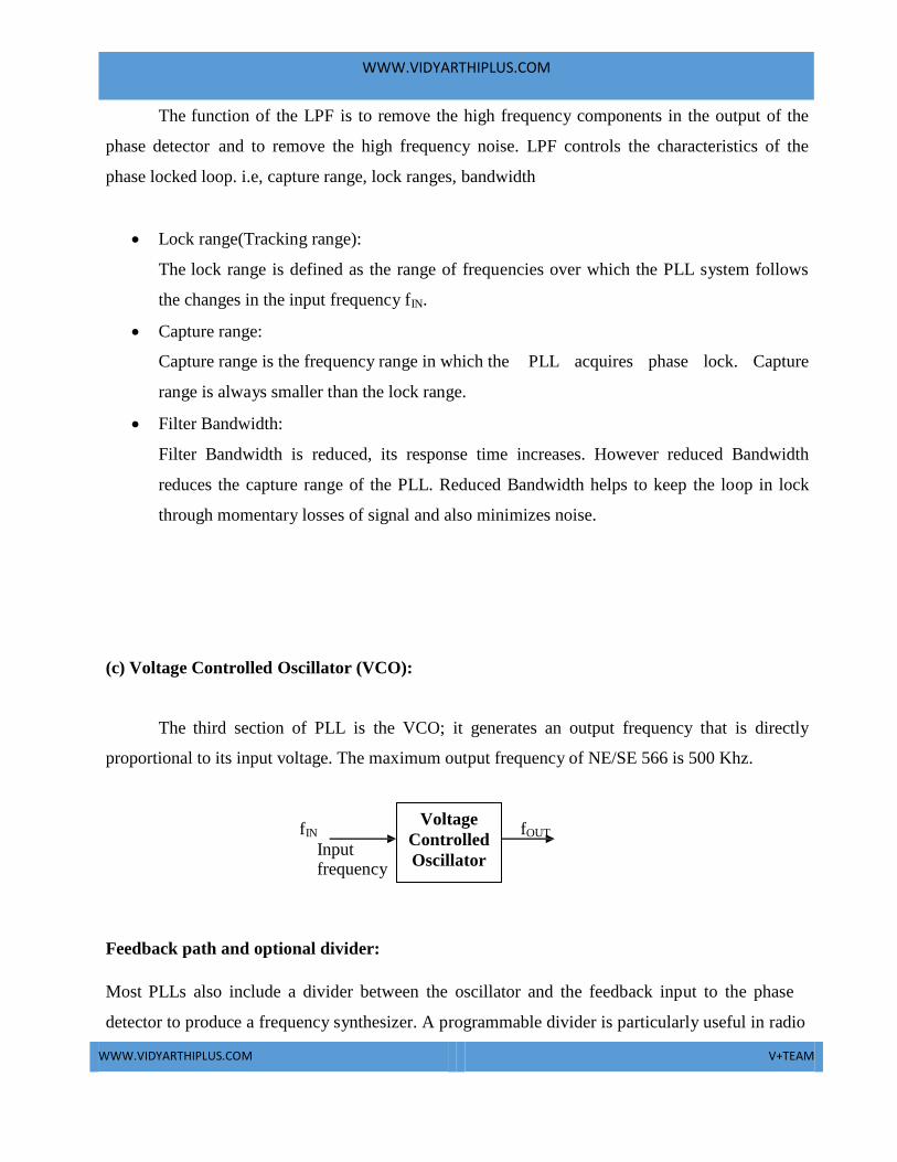
(c) Voltage Controlled Oscillator (VCO):
The third section of PLL is the VCO; it generates an output frequency that is directly
proportional to its input voltage. The maximum output frequency of NE/SE 566 is 500 Khz.
fIN
Input frequency
Feedback path and optional divider:
Voltage
Controlled
Oscillator
fOUT
Most PLLs also include a divider between the oscillator and the feedback input to the phase
detector to produce a frequency synthesizer. A programmable divider is particularly useful in radio
WWW.VIDYARTHIPLUS.COM
WWW.VIDYARTHIPLUS.COM V+TEAM
transmitter applications, since a large number of transmit frequencies can be produced from a
single stable, accurate, but expensive, quartz crystal–controlled reference oscillator.
Some PLLs also include a divider between the reference clock and the reference input to the phase
detector. If this divider divides by M, it allows the VCO to multiply the reference frequency by N
/ M. It might seem simpler to just feed the PLL a lower frequency, but in some cases the reference
frequency may be constrained by other issues, and then the reference divider is useful. Frequency
multiplication in a sense can also be attained by locking the PLL to the 'N'th harmonic of the
signal.
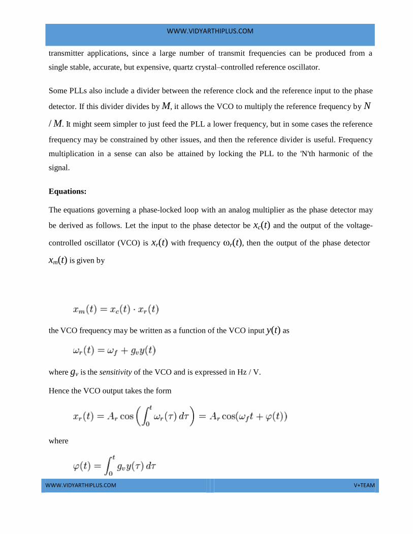
Equations:
The equations governing a phase-locked loop with an analog multiplier as the phase detector may
be derived as follows. Let the input to the phase detector be xc(t) and the output of the voltage-
controlled oscillator (VCO) is xr(t) with frequency ωr(t), then the output of the phase detector
xm(t) is given by
the VCO frequency may be written as a function of the VCO input y(t) as
where gv is the sensitivity of the VCO and is expressed in Hz / V.
Hence the VCO output takes the form
where
WWW.VIDYARTHIPLUS.COM
WWW.VIDYARTHIPLUS.COM V+TEAM
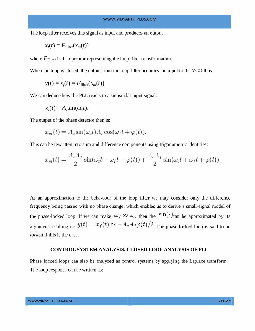
The loop filter receives this signal as input and produces an output
xf(t) = Ffilter(xm(t))
where FFilter is the operator representing the loop filter transformation.
When the loop is closed, the output from the loop filter becomes the input to the VCO thus
y(t) = xf(t) = Ffilter(xm(t)) We can deduce how the PLL reacts to a sinusoidal input signal:
xc(t) = Acsin(ωct). The output of the phase detector then is:
This can be rewritten into sum and difference components using trigonometric identities:
As an approximation to the behaviour of the loop filter we may consider only the difference
frequency being passed with no phase change, which enables us to derive a small-signal model of
the phase-locked loop. If we can make , then the can be approximated by its
argument resulting in: . The phase-locked loop is said to be
locked if this is the case.
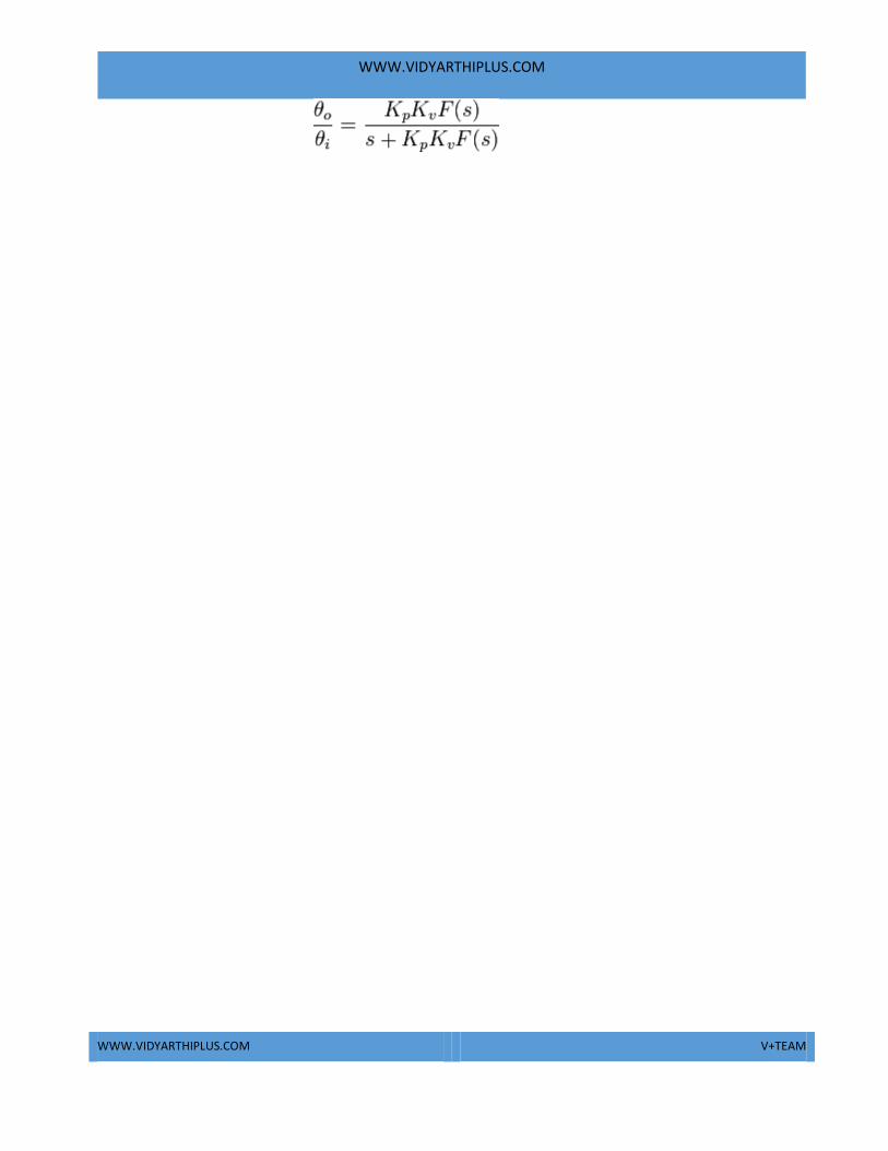
CONTROL SYSTEM ANALYSIS/ CLOSED LOOP ANALYSIS OF PLL
Phase locked loops can also be analyzed as control systems by applying the Laplace transform.
The loop response can be written as:
WWW.VIDYARTHIPLUS.COM
WWW.VIDYARTHIPLUS.COM V+TEAM
WWW.VIDYARTHIPLUS.COM
WWW.VIDYARTHIPLUS.COM V+TEAM
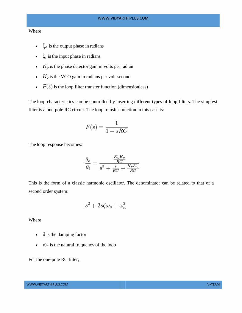
Where
ζo is the output phase in radians
ζi is the input phase in radians
Kp is the phase detector gain in volts per radian
Kv is the VCO gain in radians per volt-second
F(s) is the loop filter transfer function (dimensionless)
The loop characteristics can be controlled by inserting different types of loop filters. The simplest
filter is a one-pole RC circuit. The loop transfer function in this case is:
The loop response becomes:
This is the form of a classic harmonic oscillator. The denominator can be related to that of a
second order system:
Where
δ is the damping factor
ωn is the natural frequency of the loop
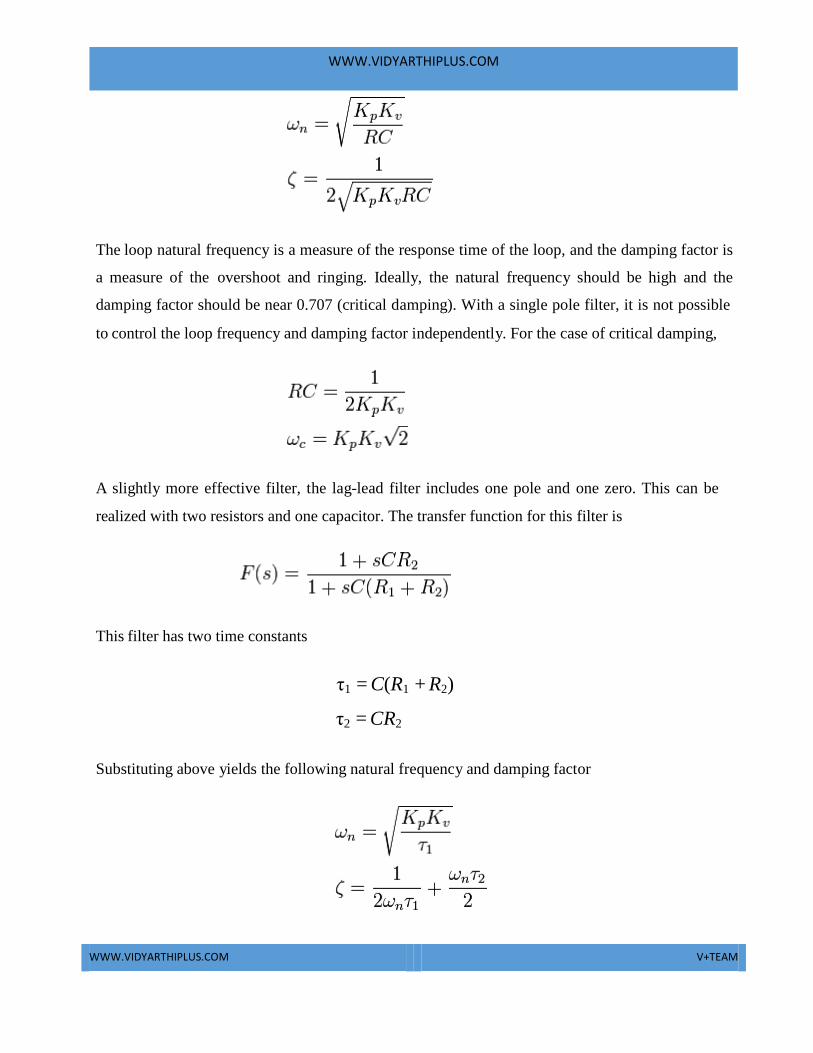
For the one-pole RC filter,
WWW.VIDYARTHIPLUS.COM
WWW.VIDYARTHIPLUS.COM V+TEAM
The loop natural frequency is a measure of the response time of the loop, and the damping factor is
a measure of the overshoot and ringing. Ideally, the natural frequency should be high and the
damping factor should be near 0.707 (critical damping). With a single pole filter, it is not possible
to control the loop frequency and damping factor independently. For the case of critical damping,
A slightly more effective filter, the lag-lead filter includes one pole and one zero. This can be
realized with two resistors and one capacitor. The transfer function for this filter is
This filter has two time constants
τ1 = C(R1 + R2)
τ2 = CR2
Substituting above yields the following natural frequency and damping factor
WWW.VIDYARTHIPLUS.COM
WWW.VIDYARTHIPLUS.COM V+TEAM
The loop filter components can be calculated independently for a given natural frequency and
damping factor
Real world loop filter design can be much more complex eg using higher order filters to reduce
various types or source of phase noise.
Applications of PLL:
The PLL principle has been used in applications such as FM stereo decoders, motor speed control,
tracking filters, FM modulation and demodulation, FSK modulation, Frequency multiplier,
Frequency synthesis etc.,
Example PLL ICs:
560 series (560, 561, 562, 564, 565 & 567)
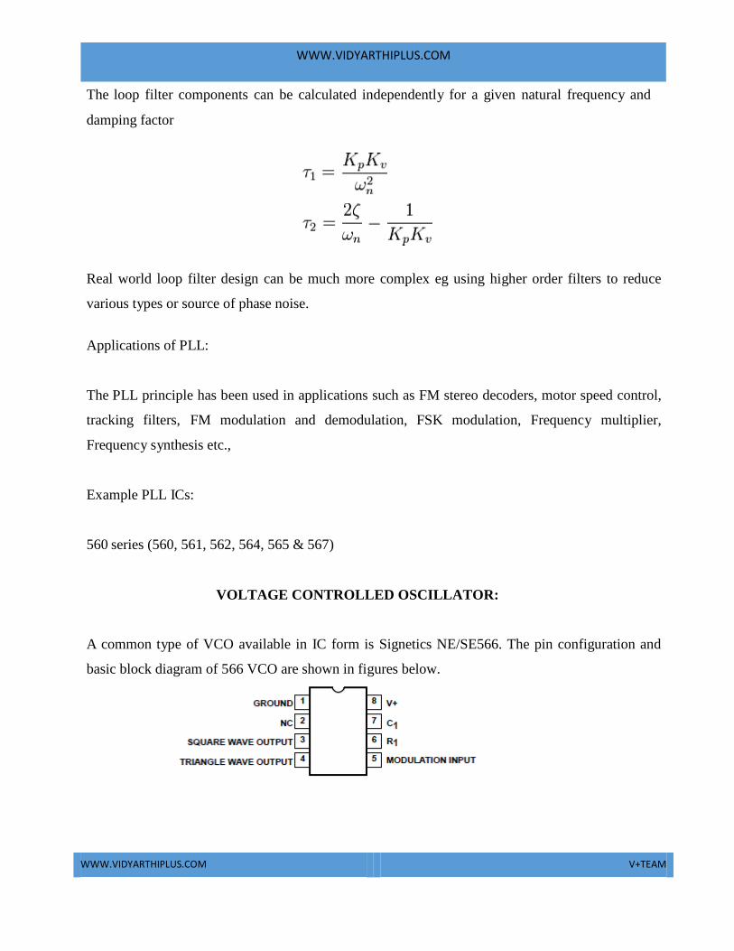
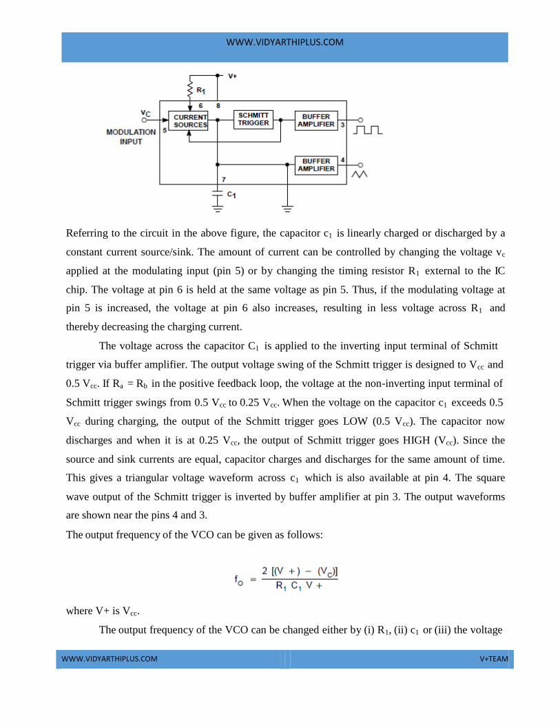
VOLTAGE CONTROLLED OSCILLATOR:
A common type of VCO available in IC form is Signetics NE/SE566. The pin configuration and
basic block diagram of 566 VCO are shown in figures below.
WWW.VIDYARTHIPLUS.COM
WWW.VIDYARTHIPLUS.COM V+TEAM
Referring to the circuit in the above figure, the capacitor c1 is linearly charged or discharged by a
constant current source/sink. The amount of current can be controlled by changing the voltage vc
applied at the modulating input (pin 5) or by changing the timing resistor R1 external to the IC
chip. The voltage at pin 6 is held at the same voltage as pin 5. Thus, if the modulating voltage at
pin 5 is increased, the voltage at pin 6 also increases, resulting in less voltage across R1 and
thereby decreasing the charging current.
The voltage across the capacitor C1 is applied to the inverting input terminal of Schmitt
trigger via buffer amplifier. The output voltage swing of the Schmitt trigger is designed to Vcc and
0.5 Vcc. If Ra = Rb in the positive feedback loop, the voltage at the non-inverting input terminal of
Schmitt trigger swings from 0.5 Vcc to 0.25 Vcc. When the voltage on the capacitor c1 exceeds 0.5
Vcc during charging, the output of the Schmitt trigger goes LOW (0.5 Vcc). The capacitor now
discharges and when it is at 0.25 Vcc, the output of Schmitt trigger goes HIGH (Vcc). Since the
source and sink currents are equal, capacitor charges and discharges for the same amount of time.
This gives a triangular voltage waveform across c1 which is also available at pin 4. The square
wave output of the Schmitt trigger is inverted by buffer amplifier at pin 3. The output waveforms
are shown near the pins 4 and 3.
The output frequency of the VCO can be given as follows:
where V+ is Vcc.
The output frequency of the VCO can be changed either by (i) R1, (ii) c1 or (iii) the voltage
WWW.VIDYARTHIPLUS.COM
WWW.VIDYARTHIPLUS.COM V+TEAM
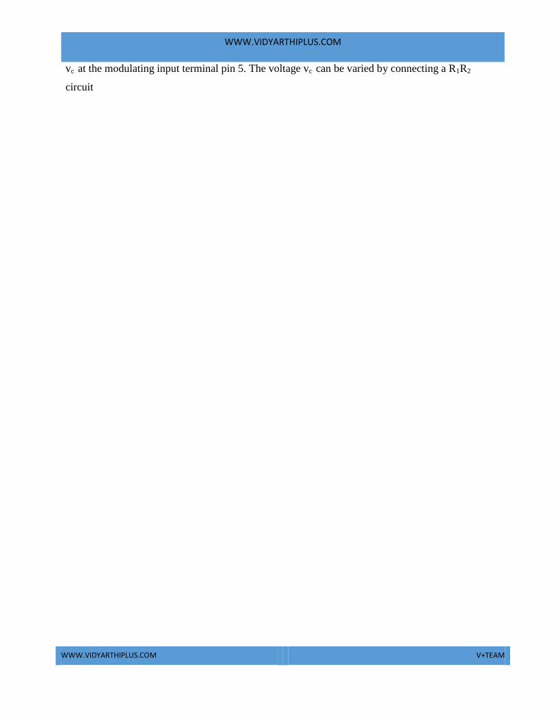
vc at the modulating input terminal pin 5. The voltage vc can be varied by connecting a R1R2
circuit
WWW.VIDYARTHIPLUS.COM
WWW.VIDYARTHIPLUS.COM V+TEAM
as shown in the figure below. The components R1and c1 are first selected so that VCO output
frequency lies in the centre of the operating frequency range. Now the modulating input voltage is
usually varied from 0.75 Vcc to Vcc which can produce a frequency variation of about 10 to 1.
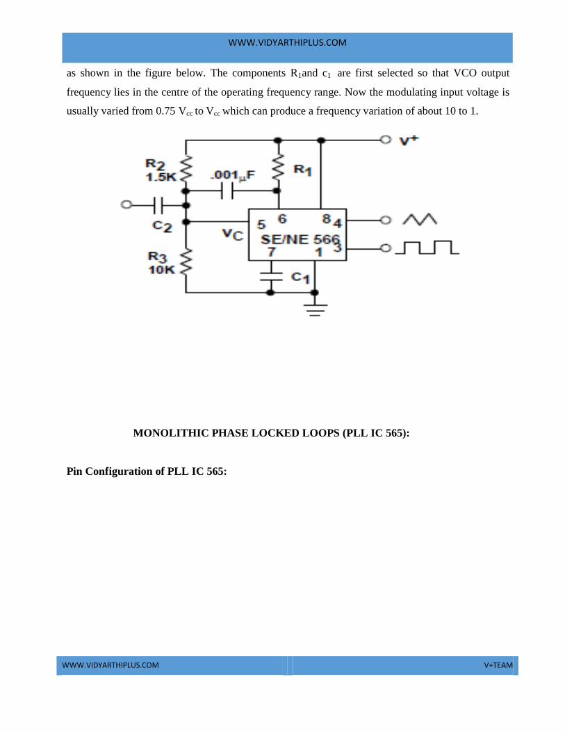
MONOLITHIC PHASE LOCKED LOOPS (PLL IC 565):
Pin Configuration of PLL IC 565:
WWW.VIDYARTHIPLUS.COM
WWW.VIDYARTHIPLUS.COM V+TEAM
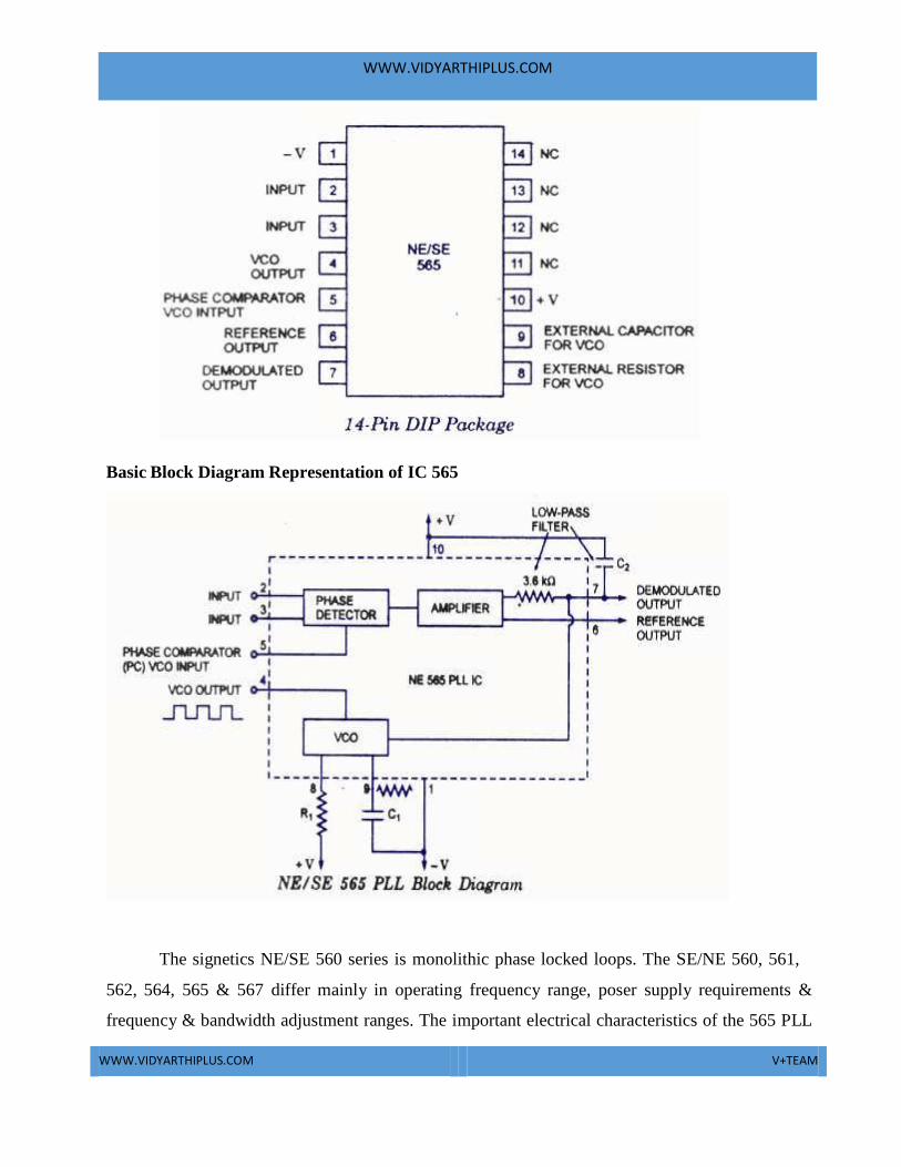
Basic Block Diagram Representation of IC 565
The signetics NE/SE 560 series is monolithic phase locked loops. The SE/NE 560, 561,
562, 564, 565 & 567 differ mainly in operating frequency range, poser supply requirements &
frequency & bandwidth adjustment ranges. The important electrical characteristics of the 565 PLL

WWW.VIDYARTHIPLUS.COM
WWW.VIDYARTHIPLUS.COM V+TEAM
are,
WWW.VIDYARTHIPLUS.COM
WWW.VIDYARTHIPLUS.COM V+TEAM
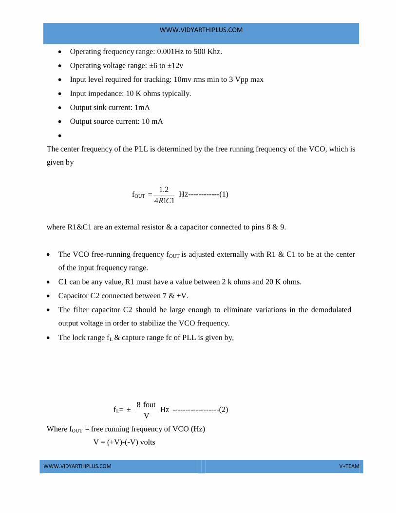
Operating frequency range: 0.001Hz to 500 Khz.
Operating voltage range: ±6 to ±12v
Input level required for tracking: 10mv rms min to 3 Vpp max
Input impedance: 10 K ohms typically.
Output sink current: 1mA
Output source current: 10 mA
The center frequency of the PLL is determined by the free running frequency of the VCO, which is
given by
fOUT = 1.2
4R1C1
HZ------------(1)
where R1&C1 are an external resistor & a capacitor connected to pins 8 & 9.
The VCO free-running frequency fOUT is adjusted externally with R1 & C1 to be at the center
of the input frequency range.
C1 can be any value, R1 must have a value between 2 k ohms and 20 K ohms.
Capacitor C2 connected between 7 & +V.
The filter capacitor C2 should be large enough to eliminate variations in the demodulated
output voltage in order to stabilize the VCO frequency.
The lock range fL & capture range fc of PLL is given by,
fL= ± 8 fout
V
Hz ------------------(2)
Where fOUT = free running frequency of VCO (Hz)
V = (+V)-(-V) volts
WWW.VIDYARTHIPLUS.COM
WWW.VIDYARTHIPLUS.COM V+TEAM
fL
fC= ±[ -------------------- ] ½
--------------(3)
(2Π)(3.6)(103)C2
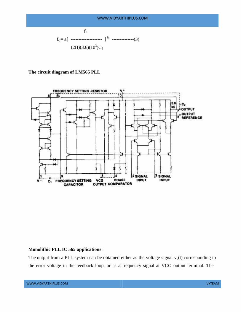
The circuit diagram of LM565 PLL
Monolithic PLL IC 565 applications:
The output from a PLL system can be obtained either as the voltage signal vc(t) corresponding to
the error voltage in the feedback loop, or as a frequency signal at VCO output terminal. The
WWW.VIDYARTHIPLUS.COM
WWW.VIDYARTHIPLUS.COM V+TEAM
voltage output is used in frequency discriminator applications whereas the frequency output is used
in signal conditioning, frequency synthesis or clock recovery applications.
Consider the case of voltage output. When PLL is locked to an input frequency, the error voltage
vc(t) is proportional to (fs-fo). If the input frequency is varied as in the case of FM signal, vc will
also vary in order to maintain the lock. Thus the voltage output serves as a frequency discriminator
which converts the input frequency changes to voltage changes.
In the case of frequency output, if the input signal is comprised of many frequency components
corrupted with noise and other disturbances, the PLL can be made to lock, selectively on one
particular frequency component at the input. The output of VCO would then regenerate that
particular frequency (because of LPF which gives output for beat frequency) and attenuate heavily
other frequencies. VCO output thus can be used for regenerating or reconditioning a desired
frequency signal (which is weak and buried in noise) out of many undesirable frequency signals.
Some of the typical applications of PLL are discussed below.
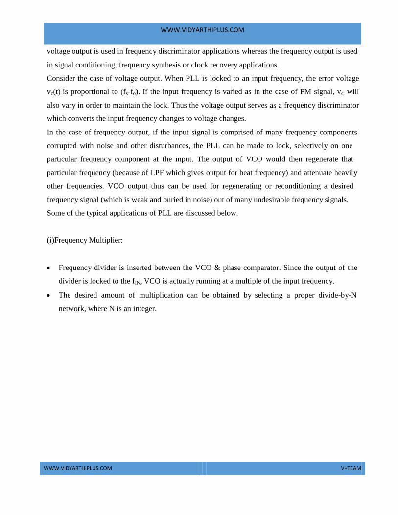
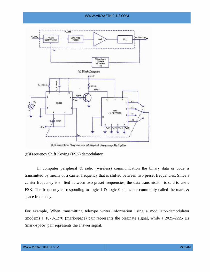
(i)Frequency Multiplier:
Frequency divider is inserted between the VCO & phase comparator. Since the output of the
divider is locked to the fIN, VCO is actually running at a multiple of the input frequency.
The desired amount of multiplication can be obtained by selecting a proper divide-by-N
network, where N is an integer.
WWW.VIDYARTHIPLUS.COM
WWW.VIDYARTHIPLUS.COM V+TEAM
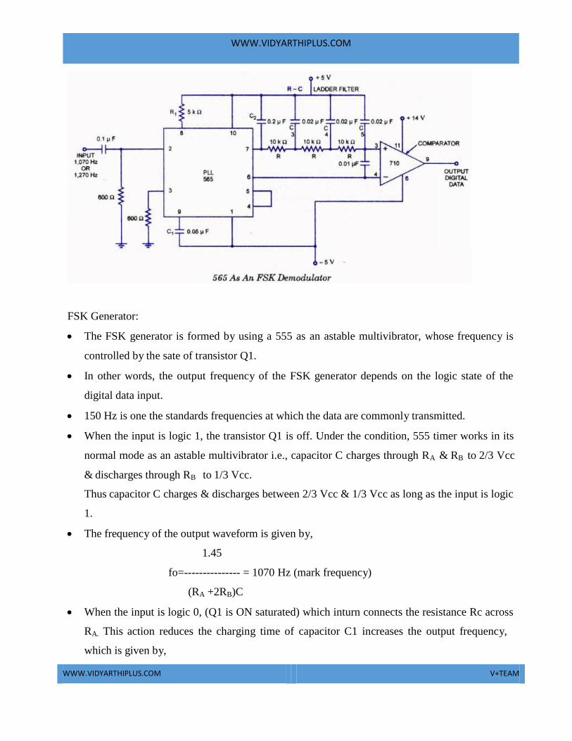
(ii)Frequency Shift Keying (FSK) demodulator:
In computer peripheral & radio (wireless) communication the binary data or code is
transmitted by means of a carrier frequency that is shifted between two preset frequencies. Since a
carrier frequency is shifted between two preset frequencies, the data transmission is said to use a
FSK. The frequency corresponding to logic 1 & logic 0 states are commonly called the mark &
space frequency.
For example, When transmitting teletype writer information using a modulator-demodulator
(modem) a 1070-1270 (mark-space) pair represents the originate signal, while a 2025-2225 Hz
(mark-space) pair represents the answer signal.
WWW.VIDYARTHIPLUS.COM
WWW.VIDYARTHIPLUS.COM V+TEAM
FSK Generator:
The FSK generator is formed by using a 555 as an astable multivibrator, whose frequency is
controlled by the sate of transistor Q1.
In other words, the output frequency of the FSK generator depends on the logic state of the
digital data input.
150 Hz is one the standards frequencies at which the data are commonly transmitted.
When the input is logic 1, the transistor Q1 is off. Under the condition, 555 timer works in its
normal mode as an astable multivibrator i.e., capacitor C charges through RA & RB to 2/3 Vcc
& discharges through RB to 1/3 Vcc.
Thus capacitor C charges & discharges between 2/3 Vcc & 1/3 Vcc as long as the input is logic
1.
The frequency of the output waveform is given by,
1.45
fo=--------------- = 1070 Hz (mark frequency)
(RA +2RB)C
When the input is logic 0, (Q1 is ON saturated) which inturn connects the resistance Rc across
RA. This action reduces the charging time of capacitor C1 increases the output frequency,
which is given by,
WWW.VIDYARTHIPLUS.COM
WWW.VIDYARTHIPLUS.COM V+TEAM
1.45
fo= ------------------ = 1270 Hz (space frequency)
(RA || RC+2 RB)C
By proper selection of resistance Rc, this frequency is adjusted to equal the space frequency of
1270 Hz. The difference between the FSK signals of 1070 Hz & 1270 Hz is 200 Hz, this
difference is called ―frequency shift‖.
The output 150 Hz can be made by connecting a voltage comparator between the output of the
ladder filter and pin 6 of PLL.
The VCO frequency is adjusted with R1 so that at fIN = 1070 Hz.
FSK Demodulator:
The output of 555 FSK generator is applied to the 565 FSK demodulator.
Capacitive coupling is used at the input to remove dc line.
At the input of 565, the loop locks to the input frequency & tracks it between the 2 frequencies.
R1 & C1 determine the free running frequency of the VCO, 3 stage RC ladder filter is used to
remove the carrier component from the output.
In digital data communication and computer peripheral, binary data is transmitted by means of a
carrier frequency which is shifted between two preset frequencies. This type of data transmission is
called frequency shift keying (FSK) technique. The binary data can be retrieved using FSK
demodulator. The figure below shows FSK demodulator using PLL for tele-typewriter signals of
1070 Hz and 1270 Hz. As the signal appears at the input, the loop locks to the input frequency and
tracks it between the two frequencies with a corresponding dc shift at the output. A three stage
filter removes the carrier component and the output signal is made logic compatible by a voltage
comparator.
WWW.VIDYARTHIPLUS.COM
WWW.VIDYARTHIPLUS.COM V+TEAM
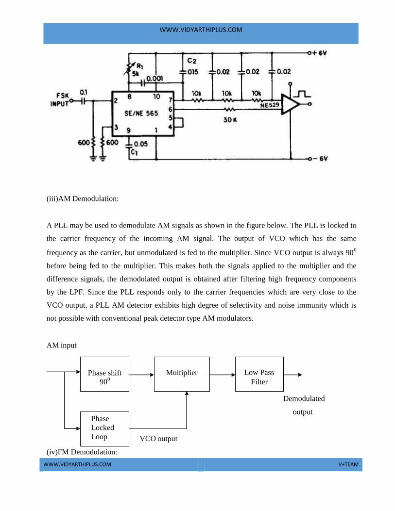
(iii)AM Demodulation:
A PLL may be used to demodulate AM signals as shown in the figure below. The PLL is locked to
the carrier frequency of the incoming AM signal. The output of VCO which has the same
frequency as the carrier, but unmodulated is fed to the multiplier. Since VCO output is always 900
before being fed to the multiplier. This makes both the signals applied to the multiplier and the
difference signals, the demodulated output is obtained after filtering high frequency components
by the LPF. Since the PLL responds only to the carrier frequencies which are very close to the
VCO output, a PLL AM detector exhibits high degree of selectivity and noise immunity which is
not possible with conventional peak detector type AM modulators.
AM input
Phase shift
900
Multiplier Low Pass
Filter
Phase
Locked
Loop
(iv)FM Demodulation:
VCO output
Demodulated
output
WWW.VIDYARTHIPLUS.COM
WWW.VIDYARTHIPLUS.COM V+TEAM
If PLL is locked to a FM signal, the VCO tracks the instantaneous frequency of the input signal.
The filtered error voltage which controls the VCO and maintains lock with the input signal is the
demodulated FM output. The VCO transfer characteristics determine the linearity of the
demodulated output. Since, VCO used in IC PLL is highly linear, it is possible to realize highly
linear FM demodulators.
(v)frequency multiplication/division:
The block diagram shown below shows a frequency multiplier/divider using PLL. A divide by N
network is inserter between the VCO output and the phase comparator input. In the locked state,
the VCO output frequency fo is given by
fo = Nfs. The multiplication factor can be obtained by selecting a proper scaling factor N of the
counter.
Frequency multiplication can also be obtained by using PLL in its harmonic locking mode. If the
input signal is rich in harmonics e.g. square wave, pulse train etc., then the VCO can be directly
locked to the n-th harmonic of the input signal without connecting any frequency divider in
between. However, as the amplitude of the higher order harmonics becomes less, effective locking
may not take place for high values of n. Typically n is kept less than 10.
The circuit of the figure above can also be used for frequency division. Since the VCO output (a
square wave) is rich in harmonics, it is possible to lock the m-th harmonic of the VCO output with
the input signal fs. The output fo of VCO is now given by
fo=fs/m
WWW.VIDYARTHIPLUS.COM
WWW.VIDYARTHIPLUS.COM V+TEAM
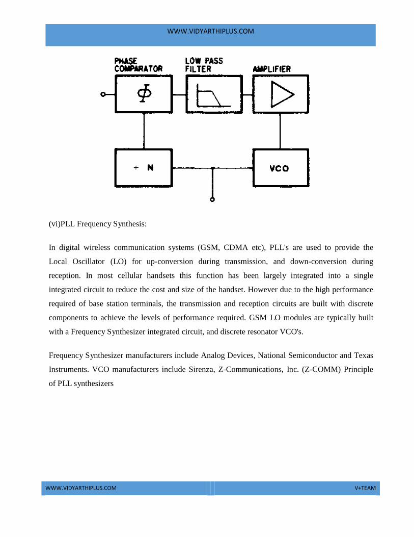
(vi)PLL Frequency Synthesis:
In digital wireless communication systems (GSM, CDMA etc), PLL's are used to provide the
Local Oscillator (LO) for up-conversion during transmission, and down-conversion during
reception. In most cellular handsets this function has been largely integrated into a single
integrated circuit to reduce the cost and size of the handset. However due to the high performance
required of base station terminals, the transmission and reception circuits are built with discrete
components to achieve the levels of performance required. GSM LO modules are typically built
with a Frequency Synthesizer integrated circuit, and discrete resonator VCO's.
Frequency Synthesizer manufacturers include Analog Devices, National Semiconductor and Texas
Instruments. VCO manufacturers include Sirenza, Z-Communications, Inc. (Z-COMM) Principle
of PLL synthesizers
WWW.VIDYARTHIPLUS.COM
WWW.VIDYARTHIPLUS.COM V+TEAM
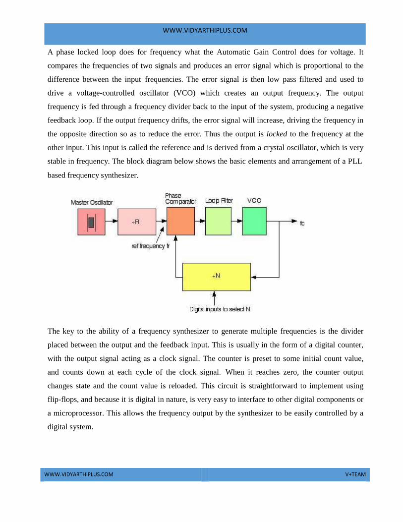
A phase locked loop does for frequency what the Automatic Gain Control does for voltage. It
compares the frequencies of two signals and produces an error signal which is proportional to the
difference between the input frequencies. The error signal is then low pass filtered and used to
drive a voltage-controlled oscillator (VCO) which creates an output frequency. The output
frequency is fed through a frequency divider back to the input of the system, producing a negative
feedback loop. If the output frequency drifts, the error signal will increase, driving the frequency in
the opposite direction so as to reduce the error. Thus the output is locked to the frequency at the
other input. This input is called the reference and is derived from a crystal oscillator, which is very
stable in frequency. The block diagram below shows the basic elements and arrangement of a PLL
based frequency synthesizer.
The key to the ability of a frequency synthesizer to generate multiple frequencies is the divider
placed between the output and the feedback input. This is usually in the form of a digital counter,
with the output signal acting as a clock signal. The counter is preset to some initial count value,
and counts down at each cycle of the clock signal. When it reaches zero, the counter output
changes state and the count value is reloaded. This circuit is straightforward to implement using
flip-flops, and because it is digital in nature, is very easy to interface to other digital components or
a microprocessor. This allows the frequency output by the synthesizer to be easily controlled by a
digital system.
WWW.VIDYARTHIPLUS.COM
WWW.VIDYARTHIPLUS.COM V+TEAM
Example:
Suppose the reference signal is 100 kHz, and the divider can be preset to any value between 1 and
100. The error signal produced by the comparator will only be zero when the output of the divider
is also 100 kHz. For this to be the case, the VCO must run at a frequency which is 100 kHz x the
divider count value. Thus it will produce an output of 100 kHz for a count of 1, 200 kHz for a
count of 2, 1 MHz for a count of 10 and so on. Note that only whole multiples of the reference
frequency can be obtained with the simplest integer N dividers. Fractional N dividers are readily
available
Practical considerations:
In practice this type of frequency synthesizer cannot operate over a very wide range of frequencies,
because the comparator will have a limited bandwidth and may suffer from aliasing problems. This
would lead to false locking situations, or an inability to lock at all. In addition, it is hard to make a
high frequency VCO that operates over a very wide range. This is due to several factors, but the
primary restriction is the limited capacitance range of varactor diodes. However, in most systems
where a synthesiser is used, we are not after a huge range, but rather a finite number over some
defined range, such as a number of radio channels in a specific band.
Many radio applications require frequencies that are higher than can be directly input to the digital
counter. To overcome this, the entire counter could be constructed using high-speed logic such as
ECL, or more commonly, using a fast initial division stage called a prescaler which reduces the
frequency to a manageable level. Since the prescaler is part of the overall division ratio, a fixed
prescaler can cause problems designing a system with narrow channel spacings - typically
encountered in radio applications. This can be overcome using a dual-modulus prescaler.[11]
Further practical aspects concern the amount of time the system can switch from channel to
channel, time to lock when first switched on, and how much noise there is in the output. All of
these are a function of the loop filter of the system, which is a low-pass filter placed between the
output of the frequency comparator and the input of the VCO. Usually the output of a frequency
comparator is in the form of short error pulses, but the input of the VCO must be a smooth noise-
WWW.VIDYARTHIPLUS.COM
WWW.VIDYARTHIPLUS.COM V+TEAM
free DC voltage. (Any noise on this signal naturally causes frequency modulation of the VCO.).
WWW.VIDYARTHIPLUS.COM
WWW.VIDYARTHIPLUS.COM V+TEAM
Heavy filtering will make the VCO slow to respond to changes, causing drift and slow response
time, but light filtering will produce noise and other problems with harmonics. Thus the design of
the filter is critical to the performance of the system and in fact the main area that a designer will
concentrate on when building a synthesizer system.

WWW.VIDYARTHIPLUS.COM
WWW.VIDYARTHIPLUS.COM V+TEAM
Related Documents