CS2252 MICROPROCESSORS & MICROCONTROLLERS Department of CSE MAHALAKSHMI ENGINEERING COLLEGE TIRUCHIRAPALLI-621213. UNIT III –MULTIPROCESSOR CONFIGURATIONS PART A (2 Marks) 1. What are tightly coupled systems or closely coupled systems? In a tightly coupled systems the microprocessor (either coprocessor or independent processors may share a common clock and bus control logic.. The two processors in a closely coupled system may communicate using a common system bus or common memory. 2. What are loosely coupled systems? In loosely coupled systems each CPU may have its own bus control logic. The bus arbitration is handled by an external circuit, common to all processors. The loosely coupled system configuration like LAN & WAN can be spreaded over a large area. 3. Write some advantages of loosely coupled systems over tightly coupled systems More number of CPUs can be added in loosely coupled systems to improve the system performance. The system structure is modular and hence easy to maintain and troubleshoot. A fault in a single module does not lead to a complete system breakdown. Due to the independent processing modules used in the system, it is more fault tolerant, more suitable to parallel applications due to its modular organizations. 4. Write some disadvantages of loosely coupled systems More complicated due to the required additional communication hardware. They are less portable and more expensive due to the additional hardware and the communication media requirement. 5. What are the multi microprocessor configuration methods.[apr/may 2009] Tightly coupled systems or closely coupled systems Loosely coupled systems 6. What is meant by Daisy chaining method? It does not require any priority resolving network, rather the priorities of all the devices are essentially assumed to be in sequence. All the masters use a single bus request line for requesting the bus access. The controller sends a bus grant signal, in response to the request, if the busy signal is inactive when the bus is free. The bus grant pulse goes to each of the masters in the sequence till it reaches a requesting master .The master then receives the grant signal, activates the busy line and gains the control of the bus. The priority is decided by the position of the requesting master in the sequence. 7. What is independent bus request scheme? Each of the masters requires a pair of request and grant pins which are connected to the controlling logic. The busy line is common for all the masters. . f the controlling logic receives a request on a bus request line, it immediately grants the bus access using the corresponding bus grant signal, provided the BUSY line is inactive, and then grants the request. This is quite fast, because each of the masters can independently communicate with the controller.

Welcome message from author
This document is posted to help you gain knowledge. Please leave a comment to let me know what you think about it! Share it to your friends and learn new things together.
Transcript
CS2252 MICROPROCESSORS & MICROCONTROLLERS Department of CSE
MAHALAKSHMI
ENGINEERING COLLEGE
TIRUCHIRAPALLI-621213.
UNIT III –MULTIPROCESSOR CONFIGURATIONS
PART A (2 Marks)
1. What are tightly coupled systems or closely coupled systems?
In a tightly coupled systems the microprocessor (either coprocessor or independent
processors may share a common clock and bus control logic.. The two processors in a closely
coupled system may communicate using a common system bus or common memory.
2. What are loosely coupled systems?
In loosely coupled systems each CPU may have its own bus control logic. The bus
arbitration is handled by an external circuit, common to all processors. The loosely coupled
system configuration like LAN & WAN can be spreaded over a large area.
3. Write some advantages of loosely coupled systems over tightly coupled systems
More number of CPUs can be added in loosely coupled systems to improve the system
performance. The system structure is modular and hence easy to maintain and
troubleshoot.
A fault in a single module does not lead to a complete system breakdown.
Due to the independent processing modules used in the system, it is more fault tolerant,
more suitable to parallel applications due to its modular organizations.
4. Write some disadvantages of loosely coupled systems
More complicated due to the required additional communication hardware.
They are less portable and more expensive due to the additional hardware and the
communication media requirement.
5. What are the multi microprocessor configuration methods.[apr/may 2009]
Tightly coupled systems or closely coupled systems
Loosely coupled systems
6. What is meant by Daisy chaining method?
It does not require any priority resolving network, rather the priorities of all the devices
are essentially assumed to be in sequence.
All the masters use a single bus request line for requesting the bus access. The controller
sends a bus grant signal, in response to the request, if the busy signal is inactive when the bus is
free. The bus grant pulse goes to each of the masters in the sequence till it reaches a requesting
master .The master then receives the grant signal, activates the busy line and gains the control of
the bus. The priority is decided by the position of the requesting master in the sequence.
7. What is independent bus request scheme? Each of the masters requires a pair of request and grant pins which are connected to the
controlling logic. The busy line is common for all the masters. . f the controlling logic receives a
request on a bus request line, it immediately grants the bus access using the corresponding bus
grant signal, provided the BUSY line is inactive, and then grants the request. This is quite fast,
because each of the masters can independently communicate with the controller.

CS2252 MICROPROCESSORS & MICROCONTROLLERS Department of CSE
8. What is meant by polling?
In polling schemes, a set of address lines is driven by the controller to address each of the
masters in sequence. When a bus request is received from a device by the controller, it generates
the address on the address lines. If the generated address matches with that of the requesting
masters, the controller activates the BUSY line.
9. Name the data types of 8087.
Binary integer
o Word
o Short
o Long
Packed decimal number(BCD)
Floating point /real number
o Short
o Long
o Temporary real
10. Explain numeric processor 8087.
Numeric processor 8087 is a coprocessor which has been designed to work under the
control of the processor 8086 and offer it additional numeric processing capabilities. It supports
16, 32, 64-bit integers 32, 64, 80-bit floating point and 16 digit BCD data types.
11. What are the functional units available in 8087?
CU-control unit
NEU - Numeric execution unit.
12. What are the advantages of multiprocessor system?
• High level performance can be attained when parallel processing.
• Robustness can be improved by isolating system functions.
13. What are the problems occurred in multiprocessor system?
1. Bus contention
2. Inter process communication
3. Resource sharing.
14. What is Coprocessor?[NOV/DEC 2007] [APR/MAY2011]
The coprocessor is a processor which specially designed for processor to work under the
control of the processor and support special processing capabilities. Example : 8087 which has
numeric processing capability and works under 8086.
15. What are the basic multiprocessor configurations?
1. Coprocessor configuration
2. Closely Coupled configuration.
3. Loosely coupled configuration.
16. Compare closely coupled and loosely coupled configurations.[NOV/DEC 2011]
Closely coupled Loosely coupled
1. Single CPU is used 1. Multiple CPU modules are used
2. It has local bus only 2. It has local as well system bus
CS2252 MICROPROCESSORS & MICROCONTROLLERS Department of CSE
3. No system memory or IO 3. It has system memory and IO, shared
4. No bus arbitration logic required 4. Bus arbitration logic required among CPU modules.
17. Write the advantages of loosely coupled system over tightly coupled systems?
1. More number of CPUs can be added in a loosely coupled system to improve the
system performance.
2. The system structure is modular and hence easy to maintain and troubleshoot.
3. A fault in a single module does not lead to a complete system breakdown.
18. What are the features of 8087?
It can operate on the data of integer, decimal and real types with lengths ranging from 2 to 10
bytes. It is high performance numeric data processor. It can multiply two 16-bit real numbers in about
27us and calculate square root in about 36us. It is multi-bus compatible.
19. Write about status bits of 8087.
S2 S1 S0 STATUS
0 X X unused
1 0 0 unused
1 0 1 READ memory
1 1 0 WRITE memory
1 1 1 Passive.
20. Write a short note on data register in 8087.
1. It has 8 data register.
2. Each register is 8 bit and accessed as a stack
3. A PUSH operation decrements the TOP of the stack by one and loads the value on the
top register.
4. A POP register stores the value from the current TOP register and increments TOP by
one.
21. Write a short note on status register in 8087.
1. Status register is 16 bit register.
2. It indicates various errors, stores condition code for certain instruction and indicates
the BUSY status.
22. Write a short note on TAG register in 8087.
TAG register holds the status of the contents of the data register.
00 - Data valid
01 - Zero
10 - A special value
11 – Empty.
23. List the data types of 8087.
• Word integer
• Short integer
• Long integer
• Packed BCD
• Short real
• Long real
• Temporary real.

CS2252 MICROPROCESSORS & MICROCONTROLLERS Department of CSE
24. What are the features of 8089 I/O processor?
• An IOP can fetch and execute its own instruction.
• IOP can transfer data from an 8 bit source to 16 bit destination and vice versa.
• Communication between IOP and CPU is through memory based control blocks.
• CPU defines tasks in the control blocks to locate a program seguence, called a
channel program.
Points to note: Each processor in the 80x86 family has a corresponding coprocessor with which it
is compatible. Math Coprocessor is known as NPX,NDP,FUP. Numeric
processor extension (NPX), Numeric data processo) (NDP),
Floating point unit (FUP). Compatible Processor and Coprocessor Processors
1. 8086 & 8088
2. 80286 3. 80386DX
4. 80386SX 5. 80486DX
6. 80486SX
Coprocessors 1. 8087
2. 80287,80287XL
3. 80287,80387DX 4. 80387SX
5. It is Inbuilt 6. 80487SX

CS2252 MICROPROCESSORS & MICROCONTROLLERS Department of CSE
Part – B (16 marks)
1. Multiprocessor systems:
Multiprocessor Systems refer to the use of multiple processors that execute instructions
simultaneously and communicate using mailboxes and semaphores
Maximum mode of 8086 is designed to implement 3 basic multiprocessor configurations:
1. coprocessor (8087)
2. closely coupled (8089)
3. loosely coupled (Multibus)
Coprocessors and closely coupled configurations are similar in that both the CPU and the external
processor share:
- Memory
- I/O system
- Bus & bus control logic
- Clock generator
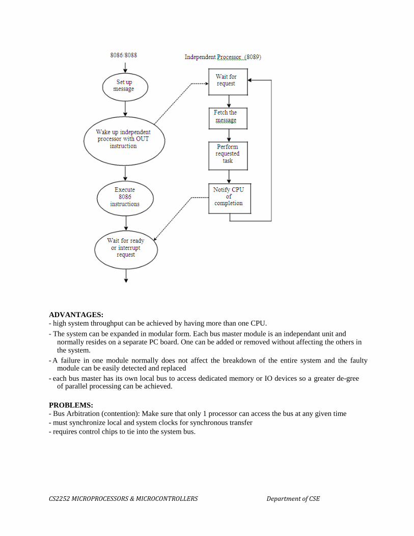
Closely Coupled Configuration:
Example: 8086/8087

CS2252 MICROPROCESSORS & MICROCONTROLLERS Department of CSE
Coprocessor cannot take control of the bus, it does everything through the CPU
- 8089 shares CPU=s clock and bus control logic - communication with host CPU is by way of shared memory - host sets up a message (command) in memory - independent processor interrupts host on completion
NOTE: Closely Coupled processor may take control of the bus independently Two 8086‟s cannot be
closely coupled.
Loosely Coupled Configuration: - has shared system bus, system memory, and system I/O - each processor has its own clock as well as its own memory (in addition to access to the
system resources, such as the system clock) clocks are of similar frequency, but asynchro-nous towards each other.
Used for medium to large multiprocessor systems Each module is capable of being the bus master
Any module could be a processor capable of being a bus master, a coprocessor configuration or a closely coupled configuration.
No direct connections between the modules. Each share the system bus and communicate through shared resources.
Processor in their separate modules can simultaneously access their private subsystems through their local busses, and perform their local data references and instruction fetches independently. This results in improved degree of concurrent processing.
Excellent for real time applications, as separate modules can be assigned specialized tasks.
CS2252 MICROPROCESSORS & MICROCONTROLLERS Department of CSE
ADVANTAGES: - high system throughput can be achieved by having more than one CPU. - The system can be expanded in modular form. Each bus master module is an independant unit and
normally resides on a separate PC board. One can be added or removed without affecting the others in the system.
- A failure in one module normally does not affect the breakdown of the entire system and the faulty
module can be easily detected and replaced - each bus master has its own local bus to access dedicated memory or IO devices so a greater de-gree
of parallel processing can be achieved.
PROBLEMS: - Bus Arbitration (contention): Make sure that only 1 processor can access the bus at any given time - must synchronize local and system clocks for synchronous transfer - requires control chips to tie into the system bus.

CS2252 MICROPROCESSORS & MICROCONTROLLERS Department of CSE
2. Architecture of 8087:
Control Unit
Execution Unit Control Unit Control unit: To synchronize the operation of the coprocessor and the processor. This unit has a Control word and Status word and Data Buffer 3.
If instruction is an ESCape (coprocessor) instruction, the coprocessor executes it, if not the microprocessor executes.
Status register reflects the over all operation of the coprocessor.

CS2252 MICROPROCESSORS & MICROCONTROLLERS Department of CSE
Status Register
15 0
B C3 ST C2 C1 C0 ES PE UE OE ZE DE IE
• C3-C0 Condition code bits
• TOP Top-of-stack (ST) • ES Error summary
• PE Precision error
• UE Under flow error
• OE Overflow error
• ZE Zero error
• DE Denormalized error
• IE Invalid error
• B Busy bit
B-Busy bit indicates that coprocessor is busy executing a task. Busy can be tested by examining the
status or by using the FWAIT instruction. Newer coprocessor automatically synchronize with the
microprocessor, so busy flag need not be tested before performing additional coprocessor tasks. C3-C0 Condition code bits indicates conditions about the coprocessor.
TOP- Top of the stack (ST) bit indicates the current register address as the top of the stack.
ES-Error summary bit is set if any unmasked error bit (PE, UE, OE, ZE, DE, or IE) is set. In the 8087
the error summary is also caused a coprocessor interrupt. PE- Precision error indicates that the result or operand executes selected precision.
UE-Under flow error indicates the result is too large to be represent with the current precision
selected by the control word. OE-Over flow error indicates a result that is too large to be represented. If this error is masked, the
coprocessor generates infinity for an overflow error. ZE-A Zero error indicates the divisor was zero while the dividend is a non-infinity or non-zero
number. DE-Denormalized error indicates at least one of the operand is denormalized. IE-Invalid error indicates
a stack overflow or underflow, indeterminate from (0/0,0,-0, etc) or the use of a NAN as an operand.
This flag indicates error such as those produced by taking the square root of a negative number.
CONTROL REGISTER
Control register selects precision, rounding control, infinity control.
It also masks an unmasks the exception bits that correspond to the rightmost Six bits of status register.
Instruction FLDCW is used to load the value into the control register.
Control Register
15 0
IC R C P C PM UM OM ZM DM IM
CS2252 MICROPROCESSORS & MICROCONTROLLERS Department of CSE
•IC Infinity control •RC Rounding control •PC Precision control
•PM Precision control •UM Underflow mask •OM Overflow mask •ZM Division by zero mask
•DM Denormalized operand mask
•IM Invalid operand mask IC –Infinity control selects either affine or projective infinity. Affine allows positive and negative
infinity, while projective assumes infinity is unsigned.
INFINITY CONTROL 0 = Projective
1 = Affine
RC –Rounding control determines the type of rounding.
ROUNDING CONTROL 00=Round to nearest or even 01=Round down towards minus infinity 10=Round up towards plus infinity 11=Chop or truncate towards zero
PC- Precision control sets the precision of he result as define in table
PRECISION CONTROL 00=Single precision (short) 01=Reserved 10=Double precision (long) 11=Extended precision (temporary)
Exception Masks – It Determines whether the error indicated by the exception affects the error bit in
the status register. If a logic1 is placed in one of the exception control bits, corresponding status register
bit is masked off.
Numeric Execution Unit This performs all operations that access and manipulate the numeric data in the coprocessor’s
registers.
Numeric registers in NUE are 80 bits wide.
NUE is able to perform arithmetic, logical and transcendental operations as well as supply a small number of mathematical constants from its on-chip ROM.
Numeric data is routed into two parts ways a 64 bit mantissa bus and a 16 bit sign/exponent bus.
3. Pin diagram of 8087:
Circuit Connection for 8086 – 8087
Multiplexed address-data bus lines are connected directly from the 8086 to 8087. The status lines
and the queue status lines connected directly from 8086 to 8087. The Request / Grant signal RQ/GT0
of 8087 is connected to RQ /GT1 of 8086.
BUSY signal 8087 is connected to TEST pin of 8086.
Interrupt output INT of the 8087 to NMI input of 8086. This intimates an error condition.

CS2252 MICROPROCESSORS & MICROCONTROLLERS Department of CSE
The main purpose of the circuitry between the INT output of 8087 and the NMI input is to make sure
that an NMI signal is not present upon reset, to make it possible to mask NMI input and to make it
possible for other devices to cause an NMI interrupt.
BHE pin is connected to the system BHE line to enable the upper bank of memory. The RQ/GT1 input
is available so that another coprocessor such as 8089 I/O processor can be connected and function in
parallel with the 8087. One type of Cooperation between the two processors that you need to know about it is how the 8087 transfers data between memory and its internal registers. When 8086
reads an 8087 instruction that needs data from memory or wants to send data to memory, the 8086 sends
out the memory address code in the instruction and sends out the appropriate memory read or memory
write signal to transfer a word of data. In the case of memory read, the addressed word will be kept on the data bus by the memory. The
8087 then simply reads the word of data bus. The 8086 ignores this word .If the 8087 only needs this one word of data, it can then go on and executes its instruction.
Some 8087 instructions need to read in or write out up to 80-bit word. For these cases 8086 outputs
the address of the first data word on the address bus and outputs the appropriate control signal. The 8087 reads the data word on the data bus by memory or writes a data word to memory on the data
bus. The 8087 grabs the 20-bit physical address that was output by the 8086.To transfer additional words
it needs to/from memory, the 8087 then takes over the buses from 8086. To take over the bus, the 8087 sends out a low-going pulse on

CS2252 MICROPROCESSORS & MICROCONTROLLERS Department of CSE
RQ/GT0 pin. The 8086 responds to this by sending another low going pulse back to the
RQ/GT0 pin of 8087 and by floating its buses. The 8087 then increments the address it grabbed during the first transfer and outputs the incremented
address on the address bus. When the 8087 output a memory read or memory write signal, another data
word will be transferred to or from the 8087.
The 8087 continues the process until it has transferred all the data words required by the instruction to/from memory.
When the 8087 is using the buses for its data transfer, it sends another low-going pulse out on its RQ/
GT0 pin to 8086 to know it can have the buses back again. The next type of the synchronization between
the host processor and the coprocessor is that required to make sure the 8086 hast does not attempt to
execute the next instruction before the 8087 has completed an instruction.
Taking one situation, in the case where the 8086 needs the data produced by the execution of an 8087 instruction to carry out its next instruction.
In the instruction sequence for example the 8087 must complete the FSTSW STATUS instruction
before the 8086 will have the data it needs to execute the MOV AX , STATUS instruction. Without some mechanism to make the 8086 wait until the 8087 completes the FSTSW
instruction, the 8086 will go on and execute the MOV AX , STATUS with erroneous data . We solve this problem by connecting the 8087 BUSY output to the TEST pin of the 8086 and putting on
the WAIT instruction in the program. While 8087 is executing an instruction it asserts its BUSY pin high. When it is finished with an
instruction, the 8087 will drop its BUSY pin low. Since the BUSY pin from 8087 is connected to the
TEST pin 8086 the processor can check its pin of 8087 whether it finished it instruction or not. You place the 8086 WAIT instruction in your program after the 8087 FSTSW instruction .When 8086 executes the WAIT instruction it enters an internal loop where it repeatedly checks the logic level on the TEST input. The 8086 will stay in this loop until it finds the TEST input asserted low, indicating the 8087 has completed its instruction. The 8086 will then exit the internal loop, fetch and execute the next instruction. Example FSTSW STATUS ;copy 8087 status word to memory MOV AX,
STATUS ;copy status word to AX to check ; bits ( a )
In this set of instructions we are not using WAIT instruction. Due to this the flow of execution of
command will takes place continuously even though the previous instruction had not finished it‟s
completion of its work .so we may lost data . FSTSW STATUS ;copy 8087 status word to memory FWAIT ;wait for 8087 to finish before- ; doing next 8086 instruction MOV AX,STATUS ;copy status word to AX to check ; bits ( b )
In this code we are adding up of FWAIT instruction so that it will stop the execution of the command
until the above instruction is finishes its work .so that you are not loosing data and after that you will
allow to continue the execution of instructions.

CS2252 – MICROPROCESSORS & MICROCONTROLLERS Department of CSE 13
Another case where you need synchronization of the processor and the coprocessor is the
case where a program has several 8087 instructions in sequence. The 8087 are executed only one instruction at a time so you have to make sure that 8087
has completed one instruction before you allow the 8086 to fetch the next 8087 instruction from memory.
Here again you use the BUSY-TEST connection and the FWAIT instruction to solve the problem. If you are hand coding, you can just put the 8086 WAIT(FWAIT) instruction after each instruction to make sure that instruction is completed before going on to next.
If you are using the assembler which accepts 8087 mnemonics, the assembler will automatically insert the 8-bit code for the WAIT instruction ,10011011 binary (9BH), as the first byte of the code for 8087 instruction.
4. Data types of 8087 processor:
Data Types
Internally, all data operands are converted to the 80-bit temporary real format.
We have 3 types.
•Integer data type
•Packed BCD data type
•Real data type
Coprocessor data types Integer Data Type Packed BCD Real data type
Example
Converting a decimal number into a Floating-point number. 1) Converting the decimal number into binary form. 2) Normalize the binary number 3) Calculate the biased exponent. 4) Store the number in the floating-point format.
Example

CS2252 – MICROPROCESSORS & MICROCONTROLLERS Department of CSE 14
Step Result 1) 100.25 2) 1100100.01 = 1.10010001 * 26 3) 110+01111111=10000101 4 ) Sign = 0 Exponent
=10000101
Significand = 10010001000000000000000 •In step 3 the biased exponent is the exponent a 26 or 110,plus a bias of 01111111(7FH) ,single precision no use 7F and double precision no use 3FFFH. •IN step 4 the information found in prior step is combined to form the floating point no.4
5. 8087 instruction set:
The 8087 instruction mnemonics begins with the letter F which stands for Floating point and distinguishes from 8086.
These are grouped into Four functional groups. 6. The 8087 detects an error condition usually called an exception when it executing an instruction it will set the bit in its Status register. 7. Types 8.
I Data transfer instructions. II Arithmetic instructions. 9. III Compare instructions. 10. IV Transcendental instructions.
(Trigonometric and Exponential) I Data Transfers Instructions:
REAL TRANSFER FLD Load real FST Store real FSTP Store real and pop FXCH Exchange registers
INTEGER TRANSFER FILD Load integer FIST Store integer FISTP Store integer and pop
PACKED DECIMAL TRANSFER(BCD) FBLD Load BCD FBSTP Store BCD and pop Example
FLD Source- Decrements the stack pointer by one and copies a real number from a stack element or memory location to the new ST. •FLD ST(3) ;Copies ST(3) to ST. •FLD LONG_REAL[BX] ;Number from memory

CS2252 – MICROPROCESSORS & MICROCONTROLLERS Department of CSE 15
;copied to ST.
FLD Destination- Copies ST to a specified stack position or to a specified memory location . •FST ST(2) ;Copies ST to ST(2),and ;increment stack pointer. •FST SHORT_REAL[BX] ;Copy ST to a memory at a ;SHORT_REAL[BX]
FXCH Destination – Exchange the contents of ST with the contents of a specified stack element. •FXCH ST(5) ;Swap ST and ST(5)
FILD Source – Integer load. Convert integer number from memory to temporary-real format and push on 8087 stack. •FILD DWORD PTR[BX] ;Short integer from memory at [BX].
FIST Destination- Integer store. Convert number from ST to integer and copy to memory. •FIST LONG_INT ;ST to memory locations named LONG_INT.
FISTP Destination-Integer store and pop. Identical to FIST except that stack pointer is
incremented after copy.
FBLD Source- Convert BCD number from memory to temporary- real format and push on top of 8087 stack.
II Arithmetic Instructions:
Four basic arithmetic functions: Addition,
Subtraction, Multiplication, and Division. Addition
FADD Add real FADDP Add real and pop FIADD Add integer
Subtraction FSUB Subtract real FSUBP Subtract real and pop FISUB Subtract integer FSUBR Subtract real reversed FSUBRP Subtract real and pop FISUBR Subtract integer reversed
Multiplication FMUL Multiply real FMULP Multiply real and pop FIMUL Multiply integer Advanced FABS Absolute value FCHS Change sign FPREM Partial remainder FPRNDINT Round to integer
FSCALE Scale
FSQRT Square root
FXTRACT Extract exponent and mantissa.

CS2252 – MICROPROCESSORS & MICROCONTROLLERS Department of CSE 16
Example FADD – Add real from specified source to specified destination Source can be a stack or memory
location. Destination must be a stack element. If no source or destination is specified, then ST is
added to ST(1) and stack pointer is incremented so that the result of addition is at ST. •FADD ST(3), ST ;Add ST to ST(3), result in ST(3)
•FADD ST,ST(4) ;Add ST(4) to ST, result in ST.
•FADD ;ST + ST(1), pop stack result at ST •FADDP ST(1) ;Add ST(1) to ST. Increment stack ;pointer so ST(1) become ST. •FIADD Car_Sold ;Integer number from memory + ST
FSUB - Subtract the real number at the specified source from the real number at the specified destination and put the result in the specified destination. •FSUB ST(2), ST ;ST(2)=ST(2) – ST. •FSUB Rate ;ST=ST – real no from memory.
•FSUB ;ST=( ST(1) – ST)
FSUBP - Subtract ST from specified stack element and put result in specified stack element .Then increment the pointer by one. •FSUBP ST(1) ;ST(1)-ST. ST(1) becomes new ST
FISUB – Integer from memory subtracted from ST, result in ST. •FISUB Cars_Sold ;ST becomes ST – integer from memory
III Compare Instructions:
Comparison FCOM Compare real FCOMP Compare real and pop FCOMPP Compare real and pop twice FICOM Compare integer FICOMP Compare integer and pop FTST Test ST against +0.0 FXAM Examine ST
III Transcendental Instruction:
Transcendental FPTAN Partial tangent FPATAN Partial arctangent F2XM1 2x - 1 FYL2X Y log2X FYL2XP1 Y log2(X+1) Example
FPTAN – Compute the values for a ratio of Y/X for an angle in ST. The angle must be in
radians, and the angle must be in the range of 0 < angle < π/4. F2XM1 – Compute Y=2x-1 for an X
value in ST. The result Y replaces X in ST. X must be in the range 0≤X≤0.5.
FYL2X - Calculate Y(LOG2X).X must be in the range of 0 < X < ∞ any Y must be in the range -∞<Y<+∞.

CS2252 – MICROPROCESSORS & MICROCONTROLLERS Department of CSE 17
FYL2XP1 – Compute the function Y(LOG2(X+1)).This instruction is almost identical to FYL2X
except that it gives more accurate results when compute log of a number very close to one. Constant Instructions. Load
Constant Instruction FLDZ Load
+0.0 FLDI Load+1.0 FLDPI Load π FLDL2T Load log210
FLDL2E Load log2e
FLDLG2 Load log102
FLDLN2 Load loge2 ALGORITHM
To calculate x to the power of y •Load base, power. •Compute (y )*( log2 x) •Separate integer(i) ,fraction(f) of a real number •Divide fraction (f) by 2 •Compute (2 f/2) * ( 2f/2) •xy = (2x) * (2y )
6. 8089 I/O processor:
The design of I/O subsystems is an integral and important step in computer system design.
CPUs and I/O peripherals have generally non-compatible bus and timing requirements-a fact that
can result in significant degradation in system performance . The logical solution to this problem
has been the deployment of an intelligent I/O subsystem which ... isolates the CPU from the I/O
peripherals.' T APPLICATION I CPU is therefore free to proceed at full speed with its ROGPAMS

CS2252 – MICROPROCESSORS & MICROCONTROLLERS Department of CSE 18
primary task of internal program processing and It PROGRAMS data manipulation. Control of all I/
operations is ATA BUFF then performed by an I/O processor, an integral part of the I/O subsystem. The CPU maintains supervisory control over the system and issues commands and messages to the I/O processor, which then pro- CP ceeds with al necessary peripheral control operations to complete the desired I/O transaction. The I/O processor is responsible for device initialization, record selection, I/O transfer, simple data transformation, error checking and retries, and it signals the CPU upon successful completion of the I/O transfer. Microprocessors of today (such as the Intel 80864) have attained respectable performance evels by innovative architectural and technological advances However, such advances in microprocessor performance may be seriously overshadowed by the constraints of traditional on-intelligent I/O subsystems.
The Intel 8089 I/O processor is designed to solve such problems by providing the necessary intelligence and capability to microcomputer I/O subsystems. The architecture of the I/O processor is designed to meet typical I/O system requirements, such as high speed DMA transfers, peripheral synchronization, etc., and is better suited to I/O processing than a general-purpose microprocessor. This article describes the Intel 8089 I/O processor. It contains a description of the various IOP-based system architectures and an overview of their operation. The internal architecture of the IOP and a typical application example are then given to illustrate its various features and capabilities that facilitate I/O subsystem design. The I/O processor contains two independent I/O channels and a processor on the same chip. When both channels are running concurrently, the IOP employs the following priority algorithm for channel selection: highest priority .
* DMA transfers
* chained channel program
* DMA termination second priority
* channel attention service lowest priority
* normal channel program execution
If both channels are requesting service for tasks with equal priorities, channel selection is done according to two programmable priority bits. The priority bits may specify a rotating priority or assign one channel to have higher priority than the other. The above priority selection scheme ensures fast responses for time-critical I/O operations while providing overall user programmability to perform channel selection. Register structure.
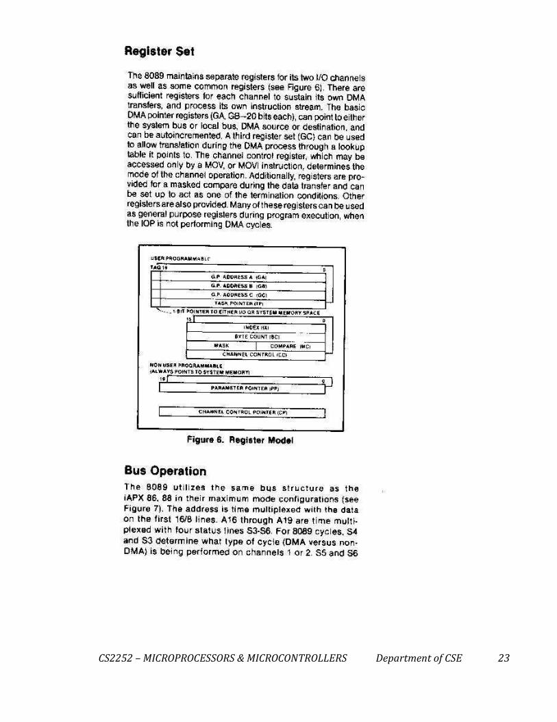
The I/O processor maintains separate register sets for each of its two I/O channels, enabling them to execute independently of one another. Each set contains 8 registers (Figure 5), and almost all of them can be used for general computation during channel program execution. Eight of the 16 registers are 21 bits wide and can be used to address one megabyte of system memory or 64K bytes of I/O space. The 21st bit is used to select the address space as system or local I/O space. The other 8 registers are 16 bits wide. The GA and GB registers are used to reference the source and destination locations during any data transfer operation. The GC register can also be used as a general register/pointer by the channel program. The task pointer serves as the channel program counter which is initialized whenever the channel is started; it can also be manipulated by the channel program. The BC register contains the number of bytes to be transferred during DMA operation and can terminate the DMA transfer if byte count termination is selected. The IX register is used as an index in the indexed addressing mode. The mask/compare register is used to perform masked byte comparisons during channel program execution and DMA operations. During program execution, the comparisons are used for conditional jumping, and in DMA, they may terminate the current DMA transfqr. The control register is a special 16-bit register which defines the channel's
CS2252 – MICROPROCESSORS & MICROCONTROLLERS Department of CSE 19
operation during DMA transfer operations.
Input-Output Processor (IOP) Instead of having each interface communicate with the CPU, a computer may incorporate
one or more external processors and assign them the task of communicating directly with all I/O devices. An input-output processor (IOP) may be classified as a processor with direct memory access capability that communicates with I/O devices. In this configuration, the computer system can be divided into a memory unit, and a number of processors comprised of the CPU and one or more IOPs. Each IOP takes care of input and output tasks, relieving the CPU from the housekeeping chores involved in I/O transfers. A processor that communicates with remote terminals over telephone and other communication media in a serial fashion is called a data communication processor (DCP).
The IOP is similar to a CPU except that it is designed to handle the details of I/O processing, Unlike the DMA controller that must be set up entirely by the CPU, the IOP can fetch and execute its own instructions. IOP instructions are specifically designed to facilitate I/O transfers. In addition, the IOP can perform other processing asks, such as arithmetic, logic, branching, and code translation. The block diagram of a computer with two processors is shown in Fig. 4-19. The memory unit occupies a central position and can communicate with each processor by means of direct memory access. The CPU is responsible for processing data needed in the solution of computation tasks. The IOP provides a path for transfer of data between various peripheral devices and the memory unit. The CPU is usually assigned the task of initiating the I/O program. From then on the IOP operates independent of the CPU and continues to transfer data from external devices and memory.
The data formats of peripheral devices differ from memory and CPU data formats. The IOP must structure data words from many different sources. For example, it may be necessary to take four bytes from an input device and pack them into one 32-bit word before the transfer to memory. Data are gathered in the IOP at the device rate and bit capacity while the CPU is executing its own program. After the input data are assembled into a memory word, they are transferred from IOP directly into memory by "stealing" one memory cycle from the CPU. Similarly, an output word transferred from memory to the IOP is directed from the IOP to the output device at the device rate and bit capacity. The communication between the IOP and the devices attached to it is similar to the program control method of transfer. Communication with the memory is similar to the direct memory access method. The way by which the CPU and IOP communicate depends on the level of sophistication included in the system. In very-large-scale computers, each processor is independent of all others and anyone processor can initiate an operation. In most computer systems, the CPU is the master while the IOP is a slave processor. The CPU is assigned the task of initiating all operations, but I/O instructions are executed in the IOP. CPU instructions provide operations to start an I/O transfer and also to test I/O status conditions needed for making decisions on various I/O activities. The IOP, in turn, typically asks for CPU attention by means of an interrupt. It also responds to CPU requests by placing a status word in a prescribed location in memory to be examined later by a CPU program. When an I/O operation is desired, the CPU informs the IOP where to find the I/O program and then leaves the transfer details to the IOP. Instructions that are read from memory by an IOP are sometimes called commands, to istinguish them from instructions that are read by the CPU. Otherwise, an instruction and a command have similar functions. Commands are prepared by experienced programmers and are stored in memory. The command words constitute the program for the IOP. The CPU informs the 10P where to find the commands in memory when it is time to execute the I/O program.

CS2252 – MICROPROCESSORS & MICROCONTROLLERS Department of CSE 20
7. 8089 I/OProcessor: 8. Features:
8. 8089 pin diagram:

CS2252 – MICROPROCESSORS & MICROCONTROLLERS Department of CSE 21

CS2252 – MICROPROCESSORS & MICROCONTROLLERS Department of CSE 22
CS2252 – MICROPROCESSORS & MICROCONTROLLERS Department of CSE 23

CS2252 – MICROPROCESSORS & MICROCONTROLLERS Department of CSE 24
9. Communication between CPU and IOP:
The communication between CPU and IOP may take different forms
depending on the particular computer considered. The sequence of operations
during CPU and IOP communication is shown in figure.
The CPU sends a test I/O instruction to IOP to test the IOP path.
The responds by inserting a status word in memory location.
The CPU refers to the status word in memory. If everything is in order, the CPU
sends the start I/O instruction to start the I/O transfer.
The IOP accesses memory for IOP program.
The CPU can now continue with another program while the IOP is busy with the
program. Both programs refer to memory by means of DMA transfer.
When the IOP terminates the execution of its program, it sends an interrupt
request to the CPU.
The CPU then issues a read I/O instruction to read the status from the IOP.
The IOP transfers the status word to memory location.
The status word indicates whether the transfer has been completed satisfactorily or
if any error has occurred during the transfer.

CS2252 – MICROPROCESSORS & MICROCONTROLLERS Department of CSE 25
Related Documents