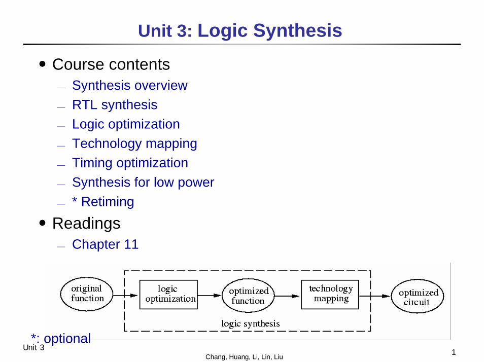
1 Chang, Huang, Li, Lin, Liu Unit 3 Unit 3: Logic Synthesis ․Course contents ⎯ Synthesis overview ⎯ RTL synthesis ⎯ Logic optimization ⎯ Technology mapping ⎯ Timing optimization ⎯ Synthesis for low power ⎯ * Retiming ․Readings ⎯ Chapter 11 *: optional

Welcome message from author
This document is posted to help you gain knowledge. Please leave a comment to let me know what you think about it! Share it to your friends and learn new things together.
Transcript
1Chang, Huang, Li, Lin, LiuUnit 3
Unit 3: Logic Synthesis
․Course contents⎯ Synthesis overview⎯ RTL synthesis⎯ Logic optimization ⎯ Technology mapping⎯ Timing optimization⎯ Synthesis for low power⎯ * Retiming
․Readings⎯ Chapter 11
*: optional

2Chang, Huang, Li, Lin, LiuUnit 3
Levels of Design
module EXP(in, s1, s2, o1, o2, o3);input in, s1, s2;output o1, o2, o3;reg o1, o2, o3;always @ (in or s1 or s2) if( s1 ) o1 = in; else o1 = o2;
always @ ( s1 or s2 or o1) begin o3 = s1 & s2; if( s2 ) o2 = o1;end
MUX0
1in
s2
s1
LATCH
QD
E
o3
o1
o2
Flowcharts, Algorithms
STRUCTURALDOMAIN
BEHAVIORALDOMAIN
PHYSICALDOMAIN
Register transfer
Boolean expression
Switch functionTransistors
Logic gates, Flip-flops
Registers, ALUs, MUXs
Processors, Memories, Buses
Transistor layout
Cells
Chips, Modules
Boards, MCMs
Circuit synthesis
Logic synthesis
Register transfer level synthesis
System synthesis
3Chang, Huang, Li, Lin, LiuUnit 3
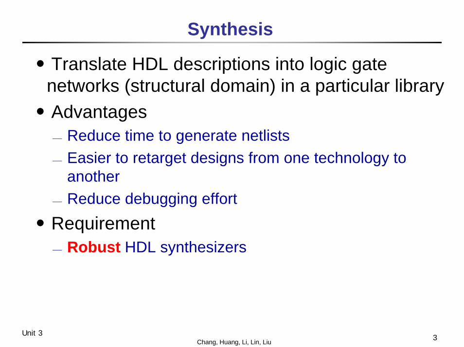
Synthesis
․Translate HDL descriptions into logic gate networks (structural domain) in a particular library
․Advantages⎯ Reduce time to generate netlists⎯ Easier to retarget designs from one technology to
another⎯ Reduce debugging effort
․Requirement⎯ Robust HDL synthesizers

4Chang, Huang, Li, Lin, LiuUnit 3
HDL Synthesis
Synthesis = Domain Translation + Optimization
Domain translation
Optimization(area, timing, power...)
--VHDL //Verilogif(A=‘1’) then if(A==1)Y<=C + D; Y=C + D;
elseif (B=‘1’) then else if(B==1)Y<=C or D; Y=C | D;
else Y<=C; else Y=C;endif
+
RTL synthesisBehavioral domain
Structural domain
5Chang, Huang, Li, Lin, LiuUnit 3
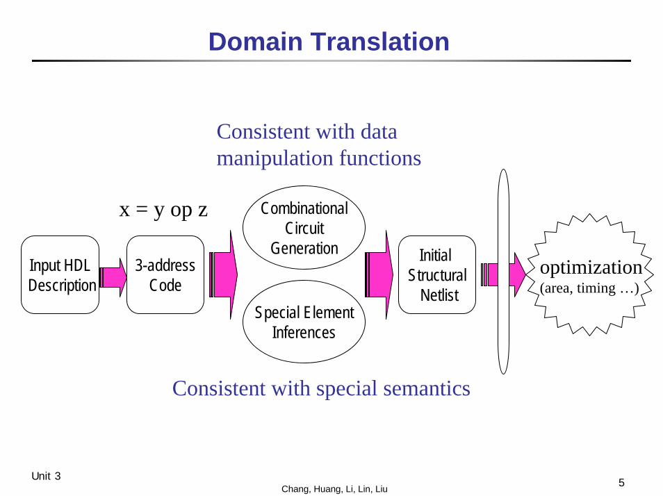
Domain Translation
Consistent with data manipulation functions
Consistent with special semantics
x = y op z
optimization(area, timing …)
CombinationalCircuit
Generation
Special ElementInferences
3-addressCode
Initial Structural
Netlist
Input HDLDescription
6Chang, Huang, Li, Lin, LiuUnit 3
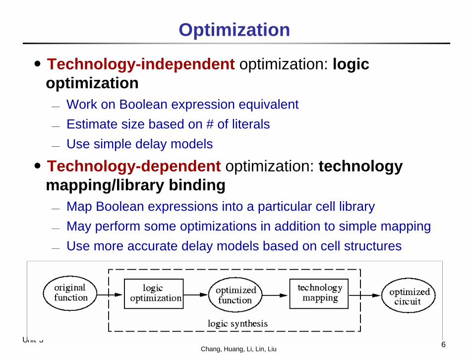
Optimization
․Technology-independent optimization: logic optimization⎯ Work on Boolean expression equivalent⎯ Estimate size based on # of literals⎯ Use simple delay models
․Technology-dependent optimization: technology mapping/library binding⎯ Map Boolean expressions into a particular cell library⎯ May perform some optimizations in addition to simple mapping⎯ Use more accurate delay models based on cell structures
7Chang, Huang, Li, Lin, LiuUnit 3
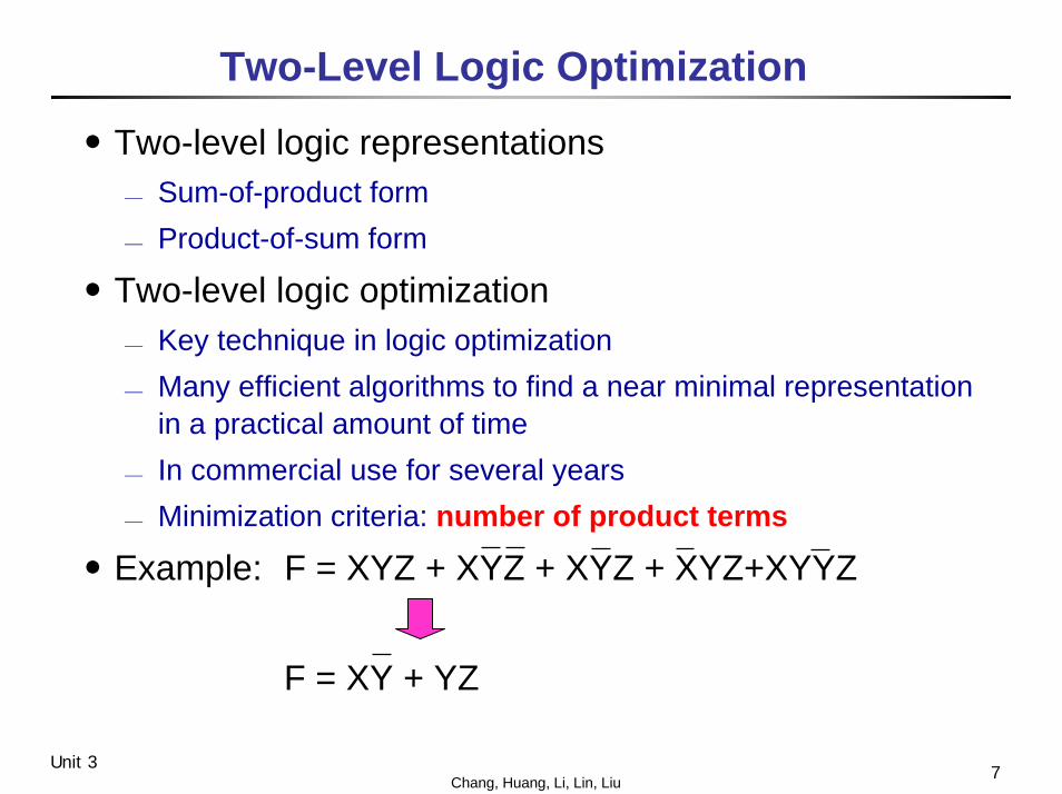
Two-Level Logic Optimization
․Two-level logic representations⎯ Sum-of-product form⎯ Product-of-sum form
․Two-level logic optimization⎯ Key technique in logic optimization⎯ Many efficient algorithms to find a near minimal representation
in a practical amount of time⎯ In commercial use for several years⎯ Minimization criteria: number of product terms
․Example: F = XYZ + XYZ + XYZ + XYZ+XYYZ
F = XY + YZ
8Chang, Huang, Li, Lin, LiuUnit 3
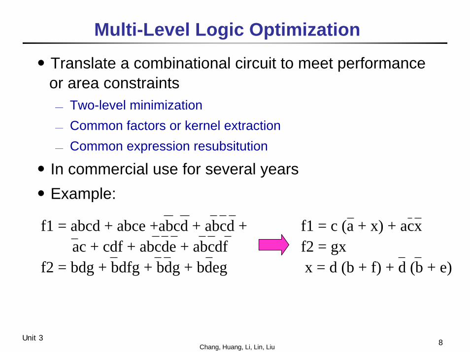
Multi-Level Logic Optimization
․Translate a combinational circuit to meet performance or area constraints⎯ Two-level minimization⎯ Common factors or kernel extraction⎯ Common expression resubsitution
․In commercial use for several years․Example:
f1 = abcd + abce +abcd + abcd +ac + cdf + abcde + abcdf
f2 = bdg + bdfg + bdg + bdeg
f1 = c (a + x) + acxf2 = gxx = d (b + f) + d (b + e)
9Chang, Huang, Li, Lin, LiuUnit 3
Technology Mapping
․Goal: translation of a technology independent representation (e.g. Boolean networks) of a circuit into a circuit in a given technology (e.g. standard cells) with optimal cost
․Optimization criteria:⎯ Minimum area⎯ Minimum delay⎯ Meeting specified timing constraints⎯ Meeting specified timing constraints with minimum area
․Usage:⎯ Technology mapping after technology independent logic
optimization⎯ Technology translation
10Chang, Huang, Li, Lin, LiuUnit 3
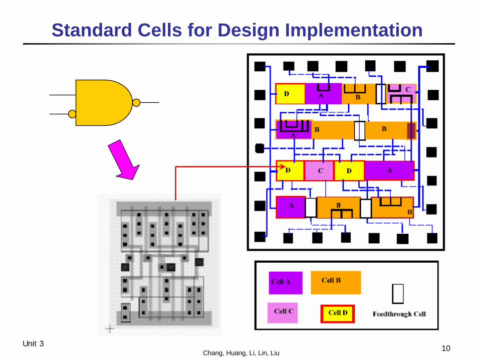
Standard Cells for Design Implementation
11Chang, Huang, Li, Lin, LiuUnit 3
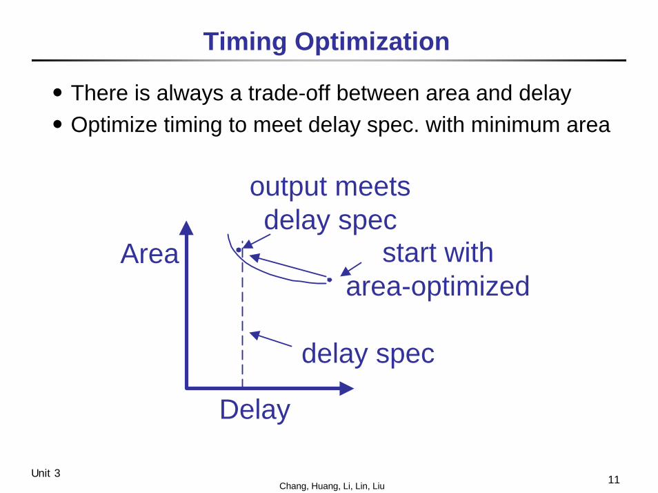
Timing Optimization
․There is always a trade-off between area and delay․Optimize timing to meet delay spec. with minimum area
output meetsdelay spec
Area
Delay
start witharea-optimized
delay spec
12Chang, Huang, Li, Lin, LiuUnit 3
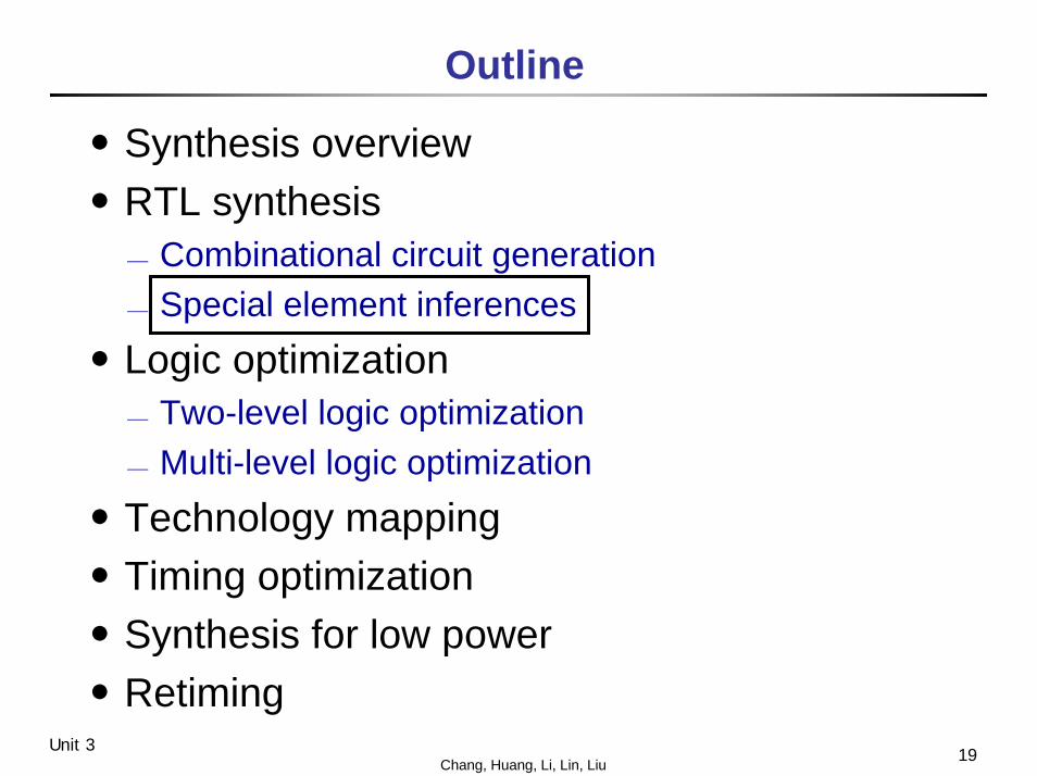
Outline
․Synthesis overview․RTL synthesis
⎯ Combinational circuit generation⎯ Special element inferences
․Logic optimization⎯ Two-level logic optimization⎯ Multi-level logic optimization
․Technology mapping․Timing optimization․Synthesis for low power․Retiming
13Chang, Huang, Li, Lin, LiuUnit 3
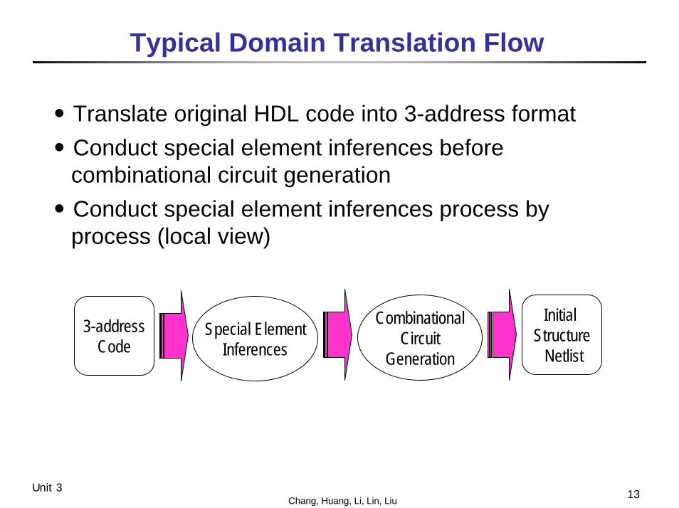
Typical Domain Translation Flow
․Translate original HDL code into 3-address format․Conduct special element inferences before
combinational circuit generation․Conduct special element inferences process by
process (local view)
3-addressCode
CombinationalCircuit
Generation
Special ElementInferences
Initial Structure
Netlist
14Chang, Huang, Li, Lin, LiuUnit 3
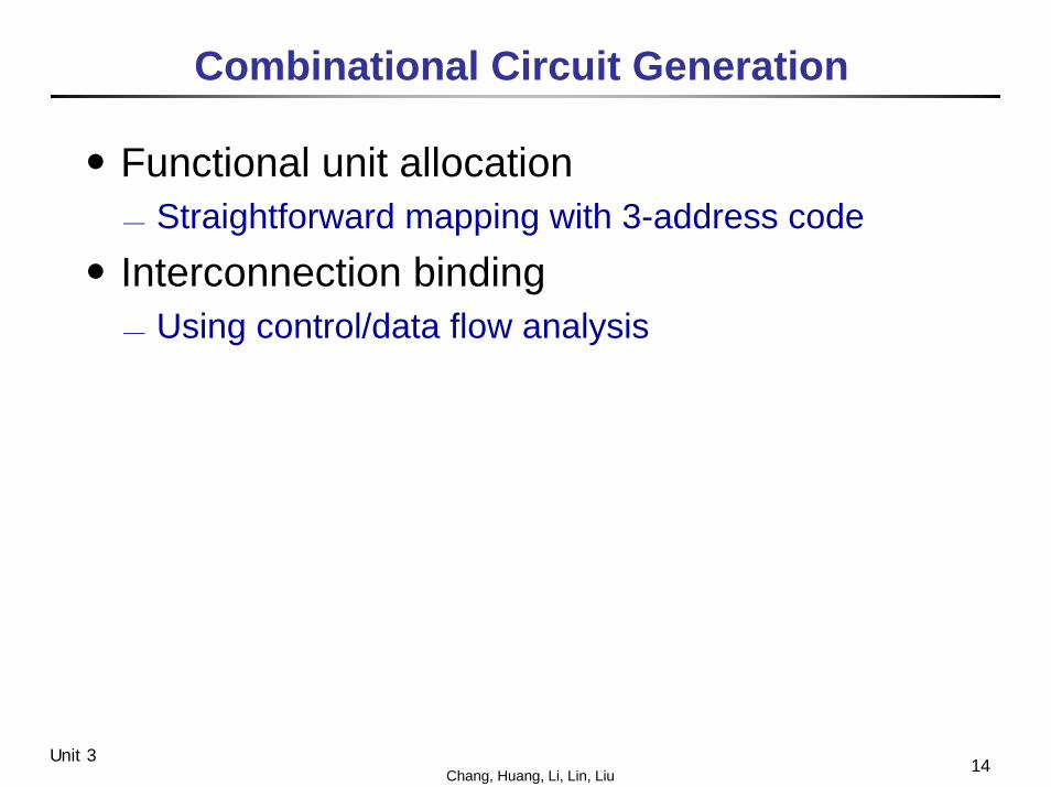
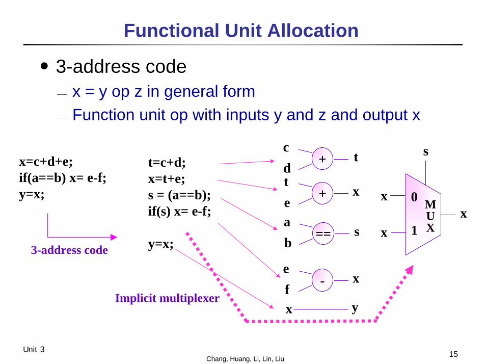
Combinational Circuit Generation
․Functional unit allocation⎯ Straightforward mapping with 3-address code
․Interconnection binding⎯ Using control/data flow analysis
15Chang, Huang, Li, Lin, LiuUnit 3
Functional Unit Allocation
․3-address code⎯ x = y op z in general form⎯ Function unit op with inputs y and z and output x
x=c+d+e;if(a==b) x= e-f;y=x;
t=c+d;x=t+e;s = (a==b);if(s) x= e-f;
y=x;==
c st+d
+t
x
ab
s
e
-ef
x
yx
0
1
xx
x
MUX
Implicit multiplexer
3-address code
16Chang, Huang, Li, Lin, LiuUnit 3
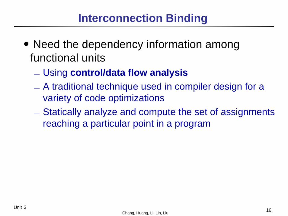
Interconnection Binding
․Need the dependency information among functional units⎯ Using control/data flow analysis⎯ A traditional technique used in compiler design for a
variety of code optimizations⎯ Statically analyze and compute the set of assignments
reaching a particular point in a program
17Chang, Huang, Li, Lin, LiuUnit 3
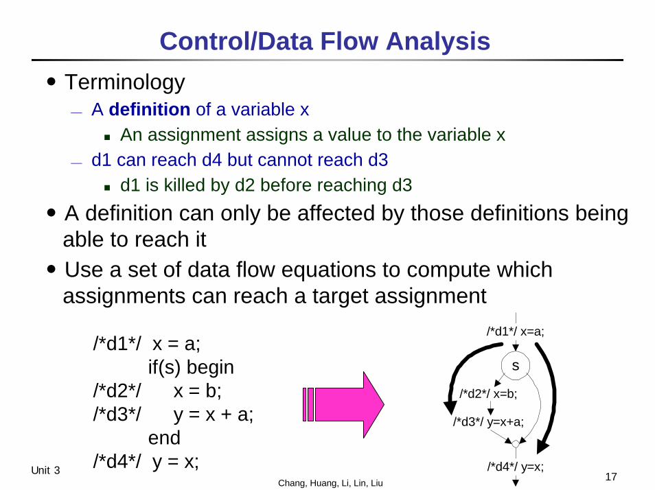
Control/Data Flow Analysis․Terminology
⎯ A definition of a variable xAn assignment assigns a value to the variable x
⎯ d1 can reach d4 but cannot reach d3d1 is killed by d2 before reaching d3
․A definition can only be affected by those definitions being able to reach it
․Use a set of data flow equations to compute which assignments can reach a target assignment
/*d1*/ x = a; if(s) begin/*d2*/ x = b;/*d3*/ y = x + a; end/*d4*/ y = x;
s
/*d1*/ x=a;
/*d4*/ y=x;
/*d2*/ x=b;
/*d3*/ y=x+a;
18Chang, Huang, Li, Lin, LiuUnit 3
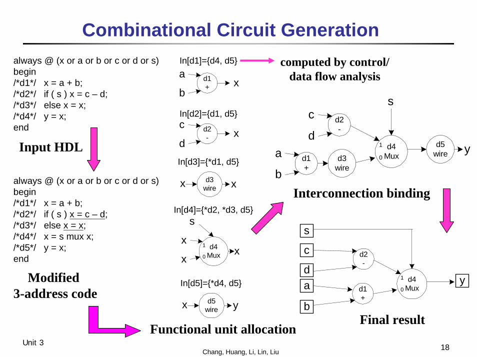
Combinational Circuit Generation
yd5wire
d4Mux
s
1
0d3wire
d2-
c
d
d1+
a
b
d4Mux
s
1
0
d2-
d1+
c
da
b
y
Functional unit allocationFinal result
Interconnection binding
Input HDL
Modified 3-address code
d1+
a
bx
d2-
c
dx
xx d3wire
yx d5wire
x
xxd4
Mux
s
1
0
In[d1]={d4, d5}
In[d2]={d1, d5}
In[d3]={*d1, d5}
In[d4]={*d2, *d3, d5}
In[d5]={*d4, d5}
computed by control/data flow analysis
always @ (x or a or b or c or d or s)begin/*d1*/ x = a + b;/*d2*/ if ( s ) x = c – d;/*d3*/ else x = x;/*d4*/ y = x;end
always @ (x or a or b or c or d or s)begin/*d1*/ x = a + b;/*d2*/ if ( s ) x = c – d;/*d3*/ else x = x;/*d4*/ x = s mux x;/*d5*/ y = x;end
19Chang, Huang, Li, Lin, LiuUnit 3
Outline
․Synthesis overview․RTL synthesis
⎯ Combinational circuit generation⎯ Special element inferences
․Logic optimization⎯ Two-level logic optimization⎯ Multi-level logic optimization
․Technology mapping․Timing optimization․Synthesis for low power․Retiming
20Chang, Huang, Li, Lin, LiuUnit 3
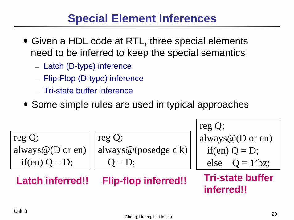
Special Element Inferences
․Given a HDL code at RTL, three special elements need to be inferred to keep the special semantics⎯ Latch (D-type) inference⎯ Flip-Flop (D-type) inference⎯ Tri-state buffer inference
․Some simple rules are used in typical approaches
reg Q;always@(D or en)
if(en) Q = D;else Q = 1’bz;
reg Q;always@(D or en)
if(en) Q = D;
reg Q;always@(posedge clk)
Q = D;Tri-state buffer inferred!!
Latch inferred!! Flip-flop inferred!!
21Chang, Huang, Li, Lin, LiuUnit 3
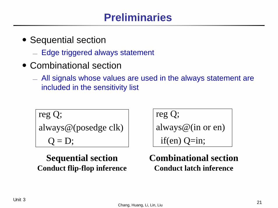
Preliminaries
․Sequential section⎯ Edge triggered always statement
․Combinational section⎯ All signals whose values are used in the always statement are
included in the sensitivity list
reg Q;always@(in or en)if(en) Q=in;
reg Q;always@(posedge clk)
Q = D;
Combinational sectionConduct latch inference
Sequential sectionConduct flip-flop inference
22Chang, Huang, Li, Lin, LiuUnit 3
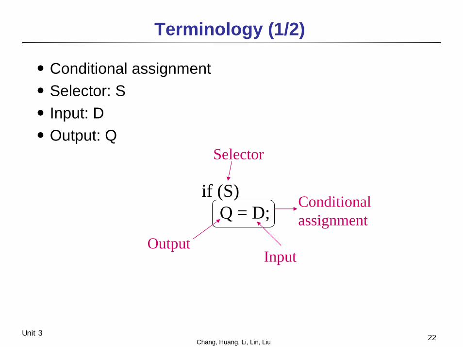
Terminology (1/2)
․Conditional assignment․Selector: S․Input: D․Output: Q
if (S) Q = D;
Selector
Conditionalassignment
InputOutput
23Chang, Huang, Li, Lin, LiuUnit 3
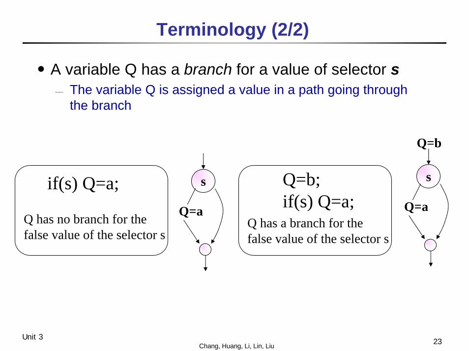
Terminology (2/2)
․A variable Q has a branch for a value of selector s⎯ The variable Q is assigned a value in a path going through
the branch
s
Q=a
Q=b
s
Q=a
Q=b;if(s) Q=a;
Q has a branch for the false value of the selector s
if(s) Q=a;
Q has no branch for the false value of the selector s
24Chang, Huang, Li, Lin, LiuUnit 3
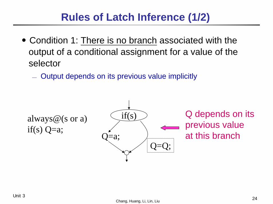
Rules of Latch Inference (1/2)
․Condition 1: There is no branch associated with the output of a conditional assignment for a value of the selector⎯ Output depends on its previous value implicitly
if(s)
Q=a;
Q depends on itsprevious value at this branch
always@(s or a)if(s) Q=a;
Q=Q;
25Chang, Huang, Li, Lin, LiuUnit 3
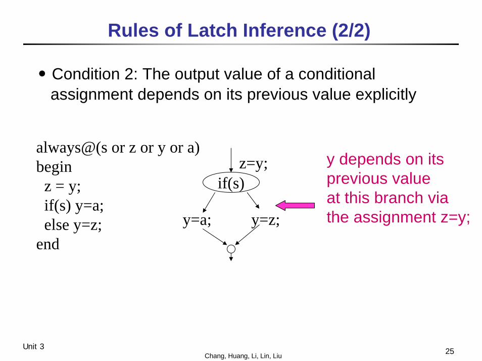
Rules of Latch Inference (2/2)
․Condition 2: The output value of a conditional assignment depends on its previous value explicitly
always@(s or z or y or a)beginz = y;if(s) y=a;else y=z;
end
y depends on itsprevious valueat this branch viathe assignment z=y;
if(s)z=y;
y=a; y=z;
26Chang, Huang, Li, Lin, LiuUnit 3
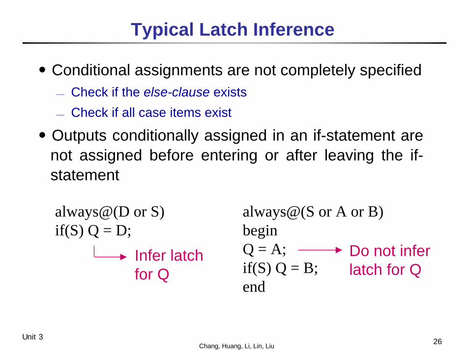
Typical Latch Inference
․Conditional assignments are not completely specified⎯ Check if the else-clause exists⎯ Check if all case items exist
․Outputs conditionally assigned in an if-statement are not assigned before entering or after leaving the if-statement
always@(D or S)if(S) Q = D;
always@(S or A or B)beginQ = A;if(S) Q = B;end
Do not infer latch for Q
Infer latchfor Q
27Chang, Huang, Li, Lin, LiuUnit 3
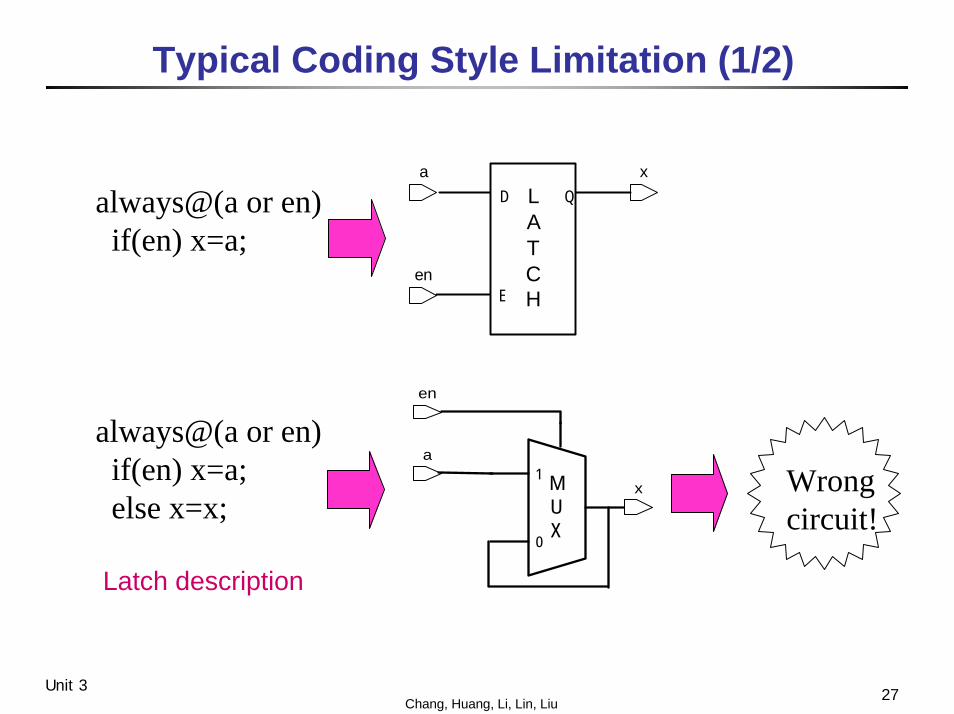
Typical Coding Style Limitation (1/2)
en
a xLATCH
QD
E
always@(a or en)if(en) x=a;
always@(a or en)if(en) x=a;else x=x;
Latch description
MUX0
1
en
x
a
Wrong circuit!
28Chang, Huang, Li, Lin, LiuUnit 3
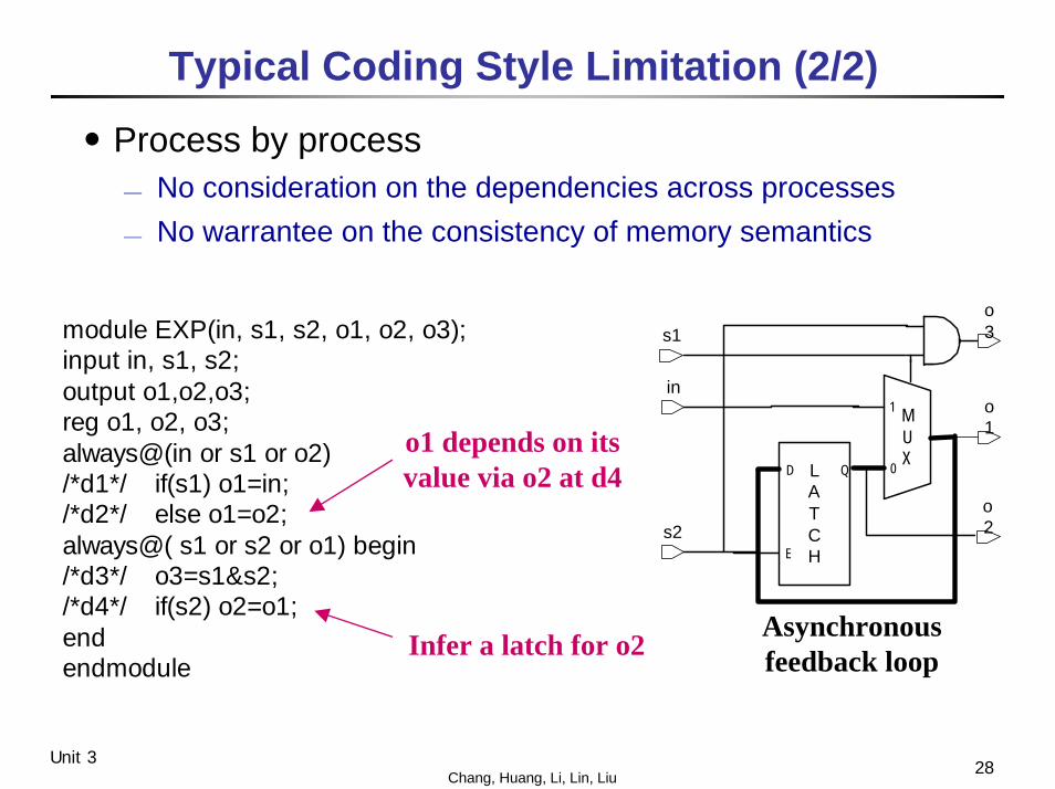
Typical Coding Style Limitation (2/2)
․Process by process⎯ No consideration on the dependencies across processes⎯ No warrantee on the consistency of memory semantics
module EXP(in, s1, s2, o1, o2, o3);input in, s1, s2;output o1,o2,o3;reg o1, o2, o3;always@(in or s1 or o2)/*d1*/ if(s1) o1=in;/*d2*/ else o1=o2;always@( s1 or s2 or o1) begin/*d3*/ o3=s1&s2;/*d4*/ if(s2) o2=o1;endendmodule
Infer a latch for o2
MUX0
1in
s2
s1
LATCH
QD
E
o3
o1
o2
Asynchronousfeedback loop
o1 depends on itsvalue via o2 at d4
29Chang, Huang, Li, Lin, LiuUnit 3
Terminology
․Clocked statement: edge-triggered always statement⎯ Simple clocked statement
e.g., always @ (posedge clock)⎯ Complex clocked statement
e.g., always @ (posedge clock or posedge reset)
․Flip-flop inference must be conducted only when synthesizing the clocked statements

30Chang, Huang, Li, Lin, LiuUnit 3
Infer FF for Simple Clocked Statements (1/2)
․Infer a flip-flop for each variable being assigned in the simple clocked statement
input a, b, s, clk;output y, w;reg x, w, y, z;always @ (posedge clk)begin/* d1 */ x = a;/* d2 */ if ( s ) y = x;/* d3 */ else y = z;/* d4 */ z = b;/* d5 */ w = 1'b1;end
aMUX
X
yz
w
by
ws
1
0
1
used after definedconnected to input of x
used before definedconnected to output of z
31Chang, Huang, Li, Lin, LiuUnit 3
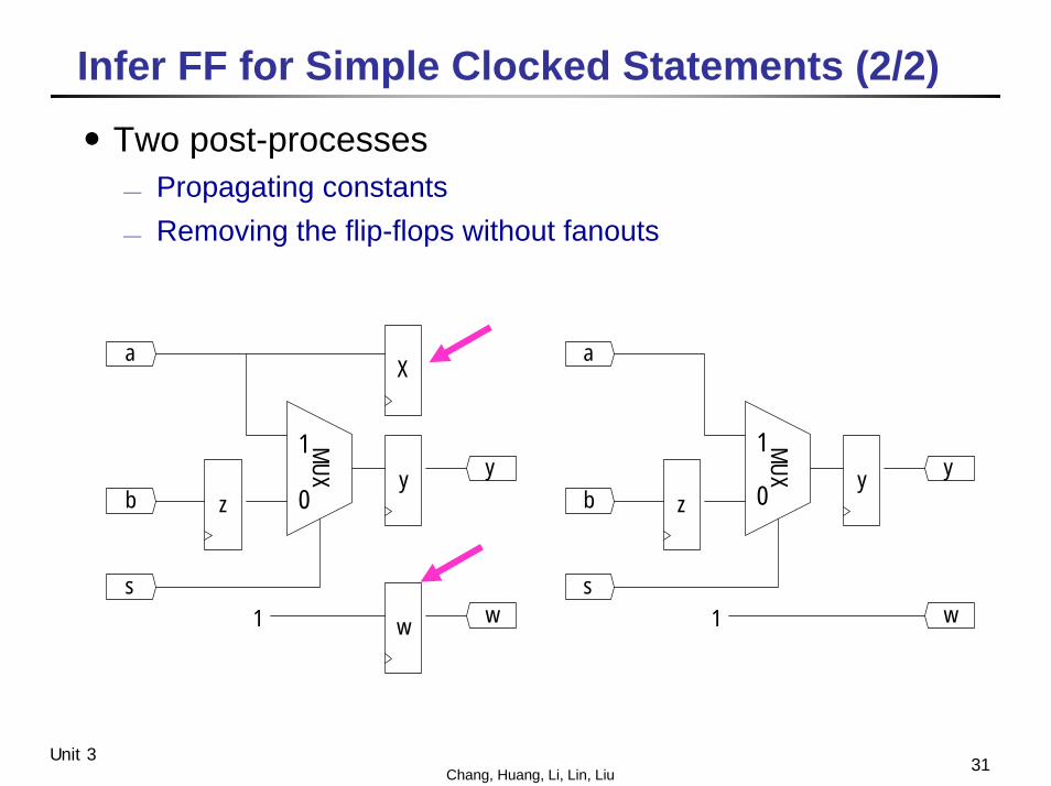
Infer FF for Simple Clocked Statements (2/2)
․Two post-processes⎯ Propagating constants ⎯ Removing the flip-flops without fanouts
a
MUX
X
yz
w
by
ws
1
0
1
a
MUX yzb
y
ws
1
0
1
32Chang, Huang, Li, Lin, LiuUnit 3
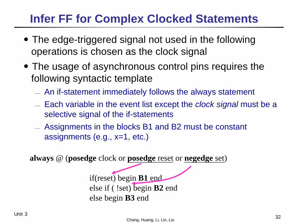
Infer FF for Complex Clocked Statements
․The edge-triggered signal not used in the following operations is chosen as the clock signal
․The usage of asynchronous control pins requires the following syntactic template⎯ An if-statement immediately follows the always statement⎯ Each variable in the event list except the clock signal must be a
selective signal of the if-statements⎯ Assignments in the blocks B1 and B2 must be constant
assignments (e.g., x=1, etc.)
always @ (posedge clock or posedge reset or negedge set)
if(reset) begin B1 endelse if ( !set) begin B2 endelse begin B3 end
33Chang, Huang, Li, Lin, LiuUnit 3
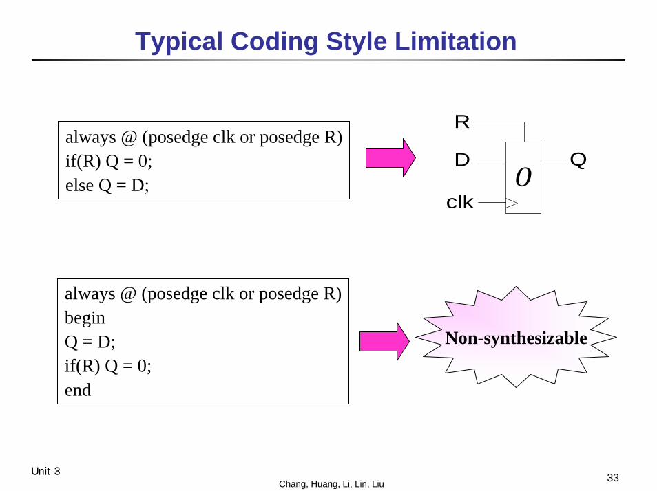
Typical Coding Style Limitation
0clk
D
R
Qalways @ (posedge clk or posedge R)if(R) Q = 0;else Q = D;
always @ (posedge clk or posedge R)beginQ = D;if(R) Q = 0;end
Non-synthesizable

34Chang, Huang, Li, Lin, LiuUnit 3
Typical Tri-State Buffer Inference (1/2)
․If a data object Q is assigned a high impedance value ‘Z’ in a multi-way branch statement (if, case, ?:)⎯ Associated Q with a tri-state buffer
․If Q associated with a tri-state buffer has also a memory attribute (latch, flip-flop)⎯ Have the Hi-Z propagation problem
Real hardware cannot propagate Hi-Z value⎯ Require two memory elements for the control and the data
inputs of tri-state buffer
reg Q;always @ (En or D)if(En) Q = D;else Q = 1'bz;
QD
En reg Q;always @ (posedge clk)if(En) Q = D;else Q = 1'bz;
QD
En

35Chang, Huang, Li, Lin, LiuUnit 3
Typical Tri-State Buffer Inference (2/2)
․It may suffer from mismatches between synthesis and simulation ⎯ Process by process ⎯ May incur the Hi-Z propagation problem
QBD
En
QA
reg QA, QB;always @ (En or D)if(En) QA = D;else QA = 1'bz;
always @ (posedge clk)QB = QA;
assignment can pass Hi-Z to QB in simulation
cannot propagate Hi-Zin real hardware
36Chang, Huang, Li, Lin, LiuUnit 3
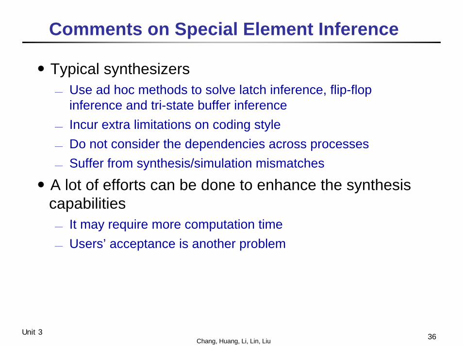
Comments on Special Element Inference
․Typical synthesizers⎯ Use ad hoc methods to solve latch inference, flip-flop
inference and tri-state buffer inference⎯ Incur extra limitations on coding style⎯ Do not consider the dependencies across processes⎯ Suffer from synthesis/simulation mismatches
․A lot of efforts can be done to enhance the synthesis capabilities⎯ It may require more computation time⎯ Users’ acceptance is another problem

37Chang, Huang, Li, Lin, LiuUnit 3
Outline
․Synthesis overview․RTL synthesis
⎯ Combinational circuit generation⎯ Special element inferences
․Logic optimization⎯ Two-level logic optimization⎯ Multi-level logic optimization
․Technology mapping․Timing optimization․Synthesis for low power․Retiming
38Chang, Huang, Li, Lin, LiuUnit 3
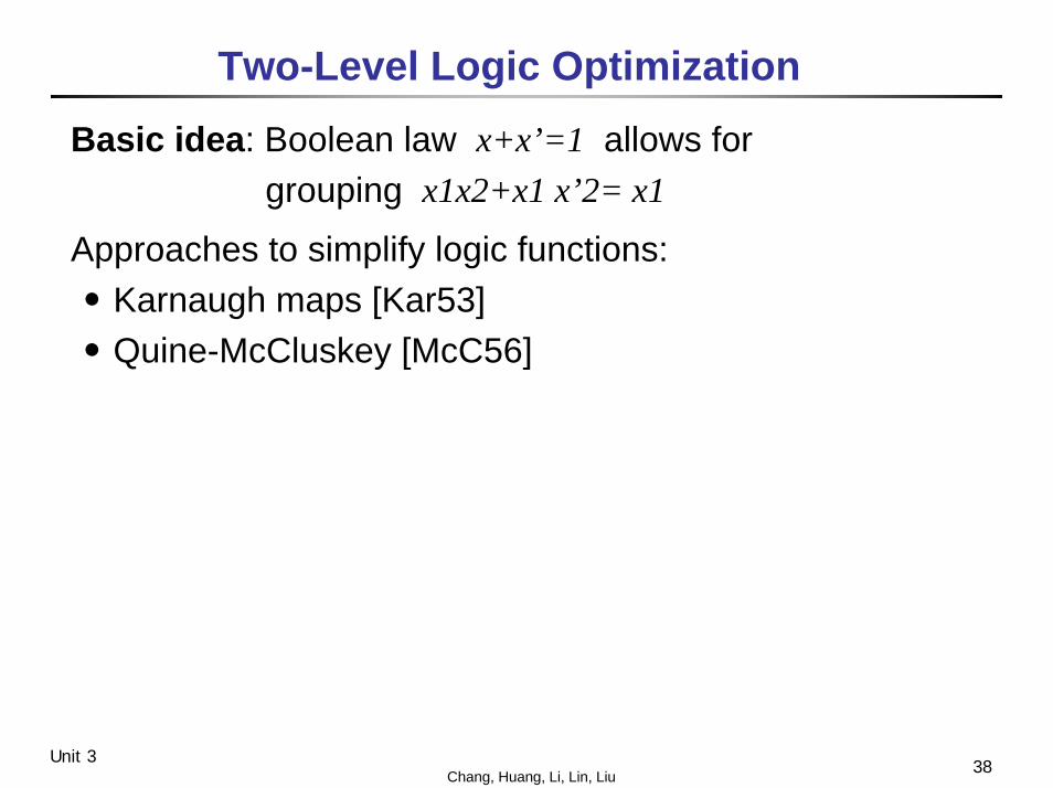
Two-Level Logic Optimization
Basic idea: Boolean law x+x’=1 allows for grouping x1x2+x1 x’2= x1
Approaches to simplify logic functions:․Karnaugh maps [Kar53]․Quine-McCluskey [McC56]
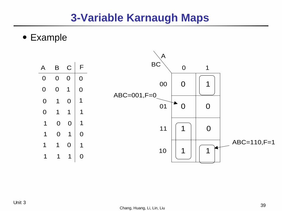
39Chang, Huang, Li, Lin, LiuUnit 3
3-Variable Karnaugh Maps
․Example
A B C F
0 0 0
0 1 1
0 1 0
0 0 1
1 0 0
1 0 1
1 1 0
1 1 1
0
0
0
0
1
1
1
1
ABC 0 1
00
01
11
10
0
0
1
1
1
0
0
1
ABC=001,F=0
ABC=110,F=1

40Chang, Huang, Li, Lin, LiuUnit 3
Implicant
․IMPLICANT:any single 1 or anygroup of 1’s combinedtogether on a mapof the function F⎯ ab’c’, abc
․PRIME IMPLICANT:an implicant thatcannot be combinedwith another termsto eliminate a variable⎯ a’b’c, a’cd, ac’
abcd 00 01 11 10
00
01
11
10
1 1
1
1
1
1
1 1
Fa'cd'
a'b'c'd'
a'b'c
ac'
ab'c'
abc'
primeimplicant
(prime implicant)
(prime implicant)

41Chang, Huang, Li, Lin, LiuUnit 3
Minimum Form
․A sum-of-products expression containing a non-prime implicant cannot be minimum⎯ Could be simplified by combining the nonprime term with
additional minterm
․To find the minimum sum-of-products⎯ Find a minimum number of prime implicants which cover all of
the 1’s⎯ Not every prime implicant is needed⎯ If prime implicants are selected in the wrong order, a
nonminimum solution may result
42Chang, Huang, Li, Lin, LiuUnit 3
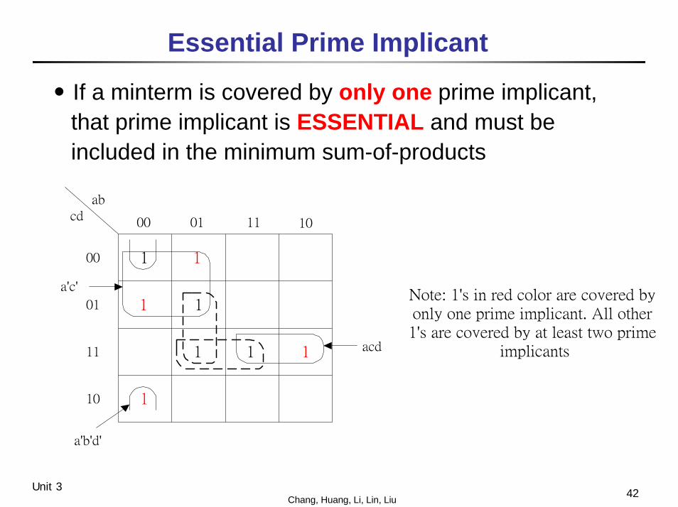
Essential Prime Implicant
․If a minterm is covered by only one prime implicant, that prime implicant is ESSENTIAL and must be included in the minimum sum-of-products
ab
cd00 01 11 10
00
01
11
10
1
11
1 1
1
1
1
a'c'
a'b'd'
Note: 1's in red color are covered by only one prime implicant. All other 1's are covered by at least two prime
implicantsacd
43Chang, Huang, Li, Lin, LiuUnit 3
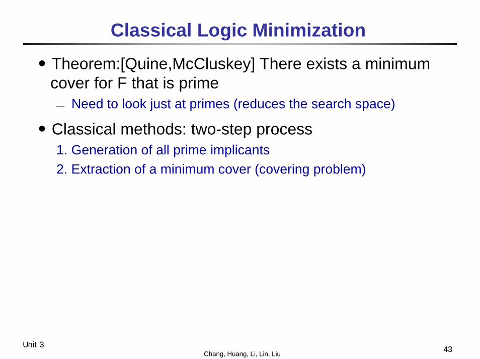
Classical Logic Minimization
․Theorem:[Quine,McCluskey] There exists a minimum cover for F that is prime⎯ Need to look just at primes (reduces the search space)
․Classical methods: two-step process1. Generation of all prime implicants2. Extraction of a minimum cover (covering problem)
44Chang, Huang, Li, Lin, LiuUnit 3
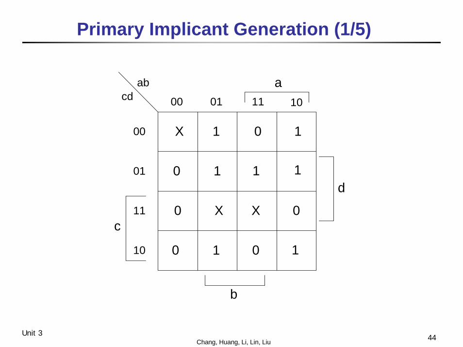
Primary Implicant Generation (1/5)
abcd 00 01 11 10
00
01
11
10
0
1
0
1
10
X
0
0
1
1
1
0
X
1
X
a
d
b
c
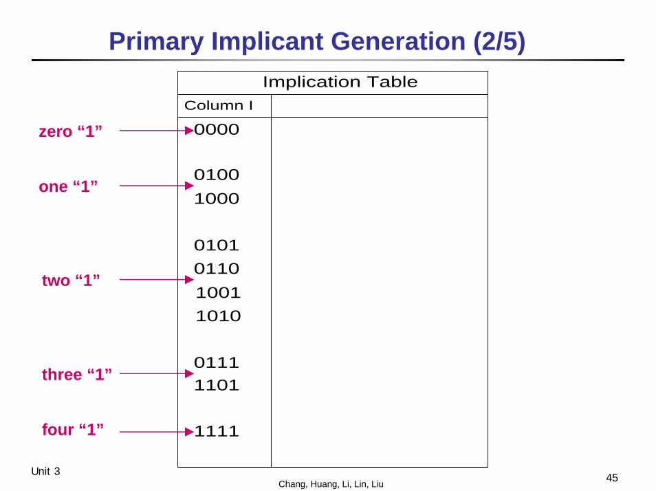
45Chang, Huang, Li, Lin, LiuUnit 3
Primary Implicant Generation (2/5)Implication Table
Column I
0000
01001000
010101101001
01111101
1111
1010
zero “1”
one “1”
two “1”
three “1”
four “1”
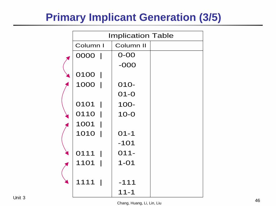
46Chang, Huang, Li, Lin, LiuUnit 3
Primary Implicant Generation (3/5)Implication Table
Column I
0000 |
0100 |1000 |
0101 |0110 |1001 |
0111 |1101 |
1111 |
1010 |
Column II
0-00-000
010-01-0100-10-0
01-1-101011-1-01
-11111-1
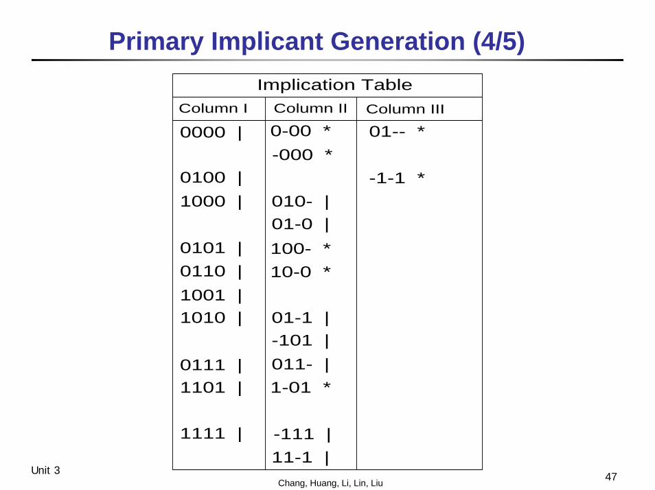
47Chang, Huang, Li, Lin, LiuUnit 3
Primary Implicant Generation (4/5)Implication Table
Column I
0000 |
0100 |1000 |
0101 |0110 |1001 |
0111 |1101 |
1111 |
1010 |
Column II
0-00 *-000 *
010- |01-0 |100- *10-0 *
01-1 |-101 |011- |1-01 *
-111 |11-1 |
Column III
01-- *
-1-1 *
48Chang, Huang, Li, Lin, LiuUnit 3
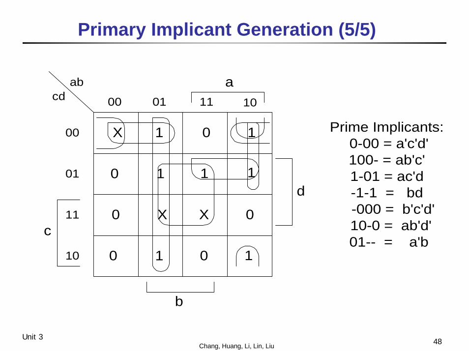
Primary Implicant Generation (5/5)
abcd 00 01 11 10
00
01
11
10
0
1
0
1
10
X
0
0
1
1
1
0
X
1
X
a
d
b
c
Prime Implicants: 0-00 = a'c'd'100- = ab'c'1-01 = ac'd-1-1 = bd
-000 = b'c'd' 10-0 = ab'd' 01-- = a'b
49Chang, Huang, Li, Lin, LiuUnit 3
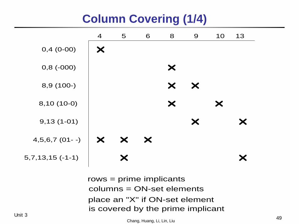
Column Covering (1/4)4 5 6 8 9 10 13
0,4 (0-00)
0,8 (-000)
8,9 (100-)
8,10 (10-0)
9,13 (1-01)
4,5,6,7 (01- -)
5,7,13,15 (-1-1)
rows = prime implicantscolumns = ON-set elementsplace an "X" if ON-set elementis covered by the prime implicant
50Chang, Huang, Li, Lin, LiuUnit 3
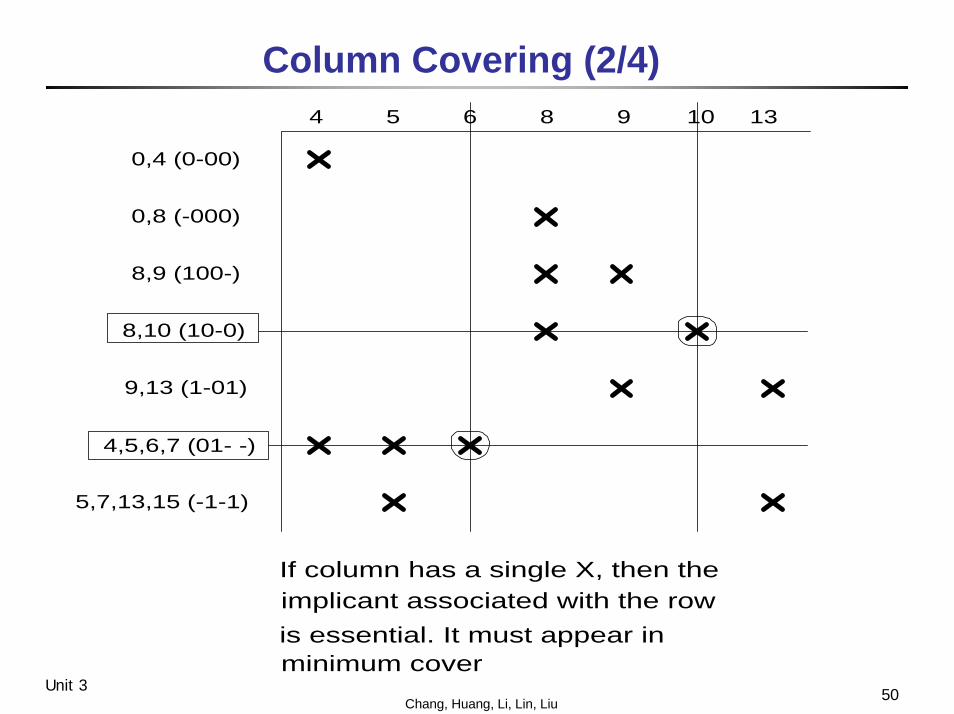
Column Covering (2/4)4 5 6 8 9 10 13
0,4 (0-00)
0,8 (-000)
8,9 (100-)
8,10 (10-0)
9,13 (1-01)
4,5,6,7 (01- -)
5,7,13,15 (-1-1)
If column has a single X, then theimplicant associated with the rowis essential. It must appear inminimum cover
51Chang, Huang, Li, Lin, LiuUnit 3
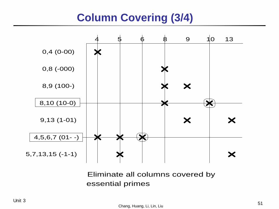
Column Covering (3/4)
4 5 6 8 9 10 13
0,4 (0-00)
0,8 (-000)
8,9 (100-)
8,10 (10-0)
9,13 (1-01)
4,5,6,7 (01- -)
5,7,13,15 (-1-1)
Eliminate all columns covered byessential primes
52Chang, Huang, Li, Lin, LiuUnit 3
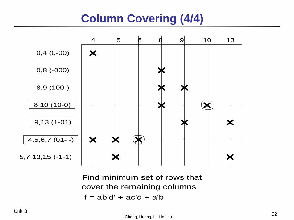
Column Covering (4/4) 4 5 6 8 9 10 13
0,4 (0-00)
0,8 (-000)
8,9 (100-)
8,10 (10-0)
9,13 (1-01)
4,5,6,7 (01- -)
5,7,13,15 (-1-1)
Find minimum set of rows thatcover the remaining columnsf = ab'd' + ac'd + a'b
53Chang, Huang, Li, Lin, LiuUnit 3
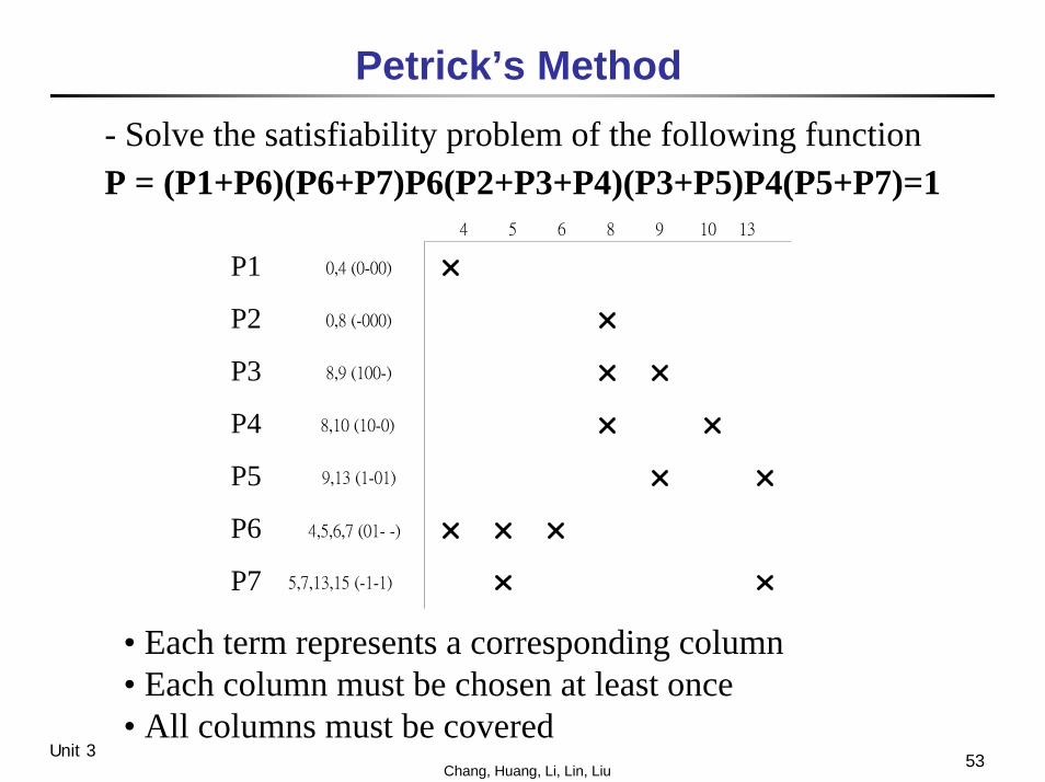
Petrick’s Method- Solve the satisfiability problem of the following functionP = (P1+P6)(P6+P7)P6(P2+P3+P4)(P3+P5)P4(P5+P7)=1
4 5 6 8 9 10 13
0,4 (0-00)
0,8 (-000)
8,9 (100-)
8,10 (10-0)
9,13 (1-01)
4,5,6,7 (01- -)
5,7,13,15 (-1-1)
P1
P2
P3
P4
P5
P6
P7
• Each term represents a corresponding column• Each column must be chosen at least once• All columns must be covered
54Chang, Huang, Li, Lin, LiuUnit 3
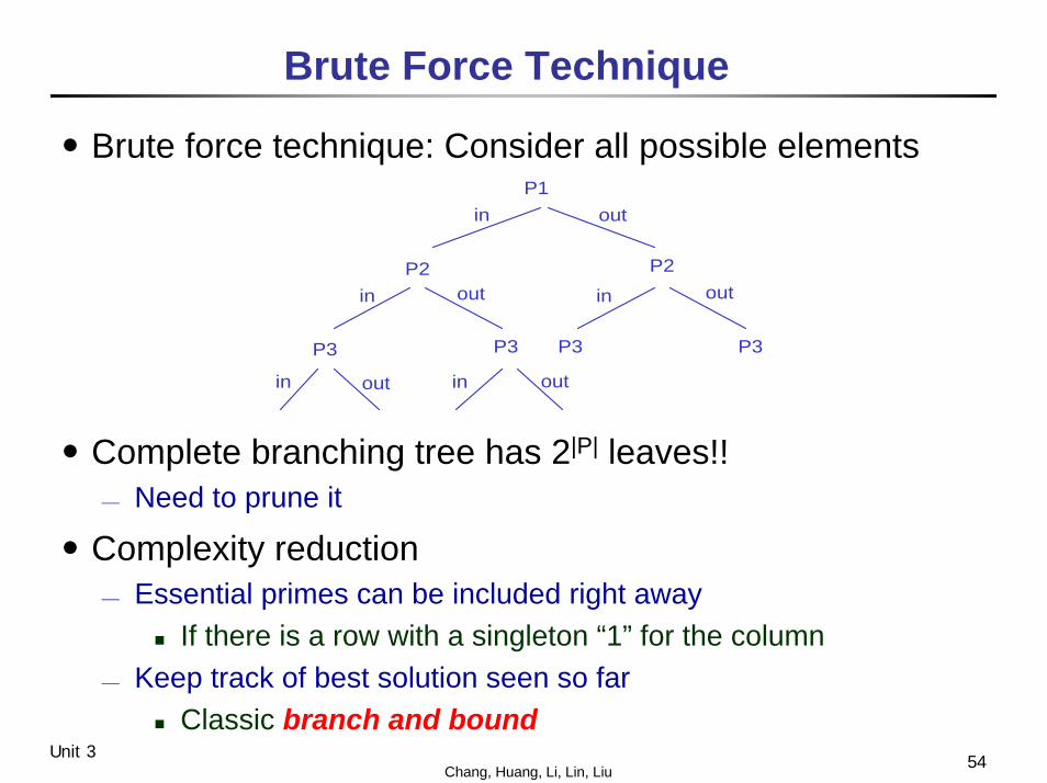
Brute Force Technique
․Brute force technique: Consider all possible elements
․Complete branching tree has 2|P| leaves!!⎯ Need to prune it
․Complexity reduction⎯ Essential primes can be included right away
If there is a row with a singleton “1” for the column⎯ Keep track of best solution seen so far
Classic branch and bound
P1in out
P2 P2
in out in out
P3 P3 P3 P3
in out in out
55Chang, Huang, Li, Lin, LiuUnit 3
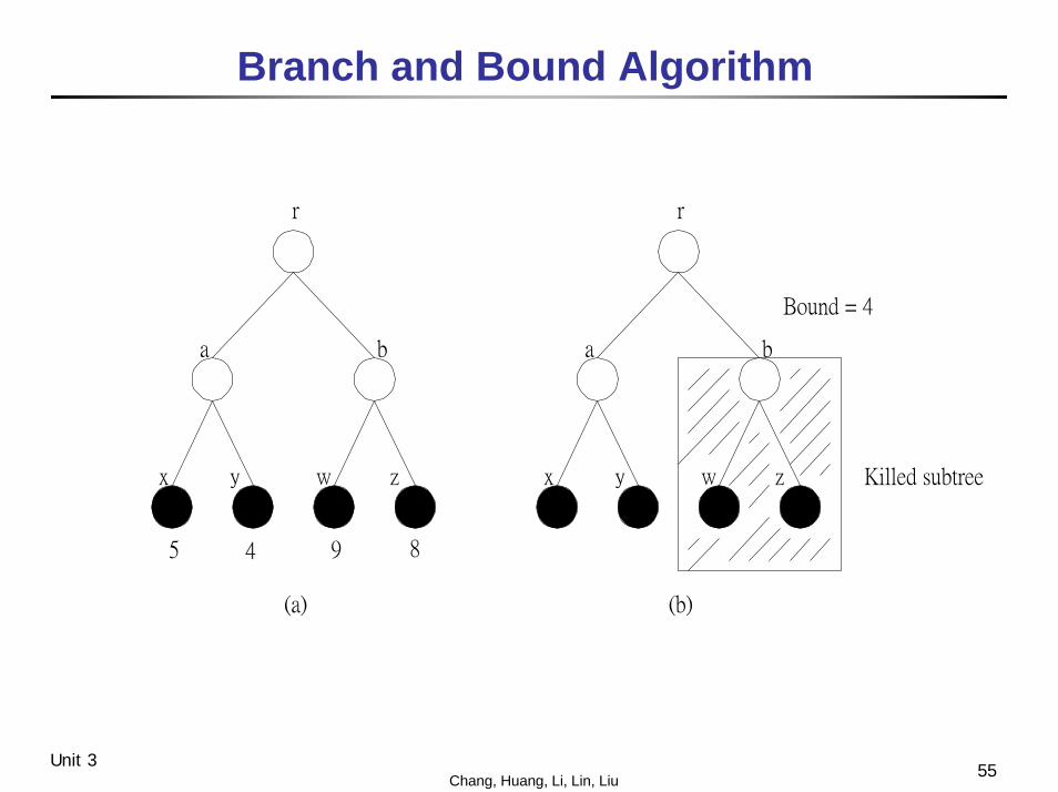
Branch and Bound Algorithm
r
a b
x y w z
r
a b
x y w z
5 4 9 8
Bound = 4
Killed subtree
(a) (b)
56Chang, Huang, Li, Lin, LiuUnit 3
Heuristic Optimization
․Generation of all prime implicants is impractical⎯ The number of prime implicants for functions with n variables is in
the order of 3n/n
․Finding an exact minimum cover is NP-hard⎯ Cannot be finished in polynomial time
․Heuristic method: avoid generation of all prime implicants․Procedure
⎯ A minterm of ON(f) is selected, and expanded until it becomes a prime implicant
⎯ The prime implicant is put in the final cover, and all minterms covered by this prime implicant are removed
⎯ Iterated until all minterms of the ON(f) are covered
․“ESPRESSO” developed by UC Berkeley⎯ The kernel of synthesis tools
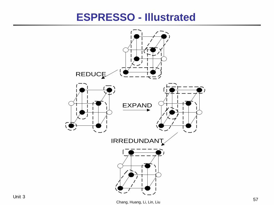
57Chang, Huang, Li, Lin, LiuUnit 3
ESPRESSO - Illustrated
REDUCE
EXPAND
IRREDUNDANT
58Chang, Huang, Li, Lin, LiuUnit 3
Outline
․Synthesis overview․RTL synthesis
⎯ Combinational circuit generation⎯ Special element inferences
․Logic optimization⎯ Two-level logic optimization⎯ Multi-level logic optimization
․Technology mapping․Timing optimization․Synthesis for low power․Retiming
59Chang, Huang, Li, Lin, LiuUnit 3
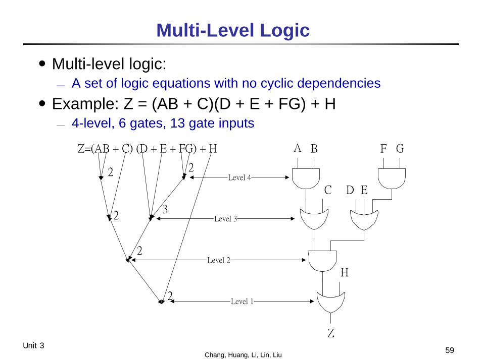
Multi-Level Logic
․Multi-level logic:⎯ A set of logic equations with no cyclic dependencies
․Example: Z = (AB + C)(D + E + FG) + H⎯ 4-level, 6 gates, 13 gate inputs
A B
C D E
F G
H
Z
Z=(AB + C) (D + E + FG) + H
Level 4
Level 3
Level 2
Level 1
2
2
2
3
2
2

60Chang, Huang, Li, Lin, LiuUnit 3
Boolean Network
․Directed acyclic graph (DAG)․Each source node is a primary input․Each sink node is a primary output․Each internal node represents an equation․Arcs represent variable dependencies
F G
Y X
a b d c
x y
fanin of y : a, bfanout of x : F
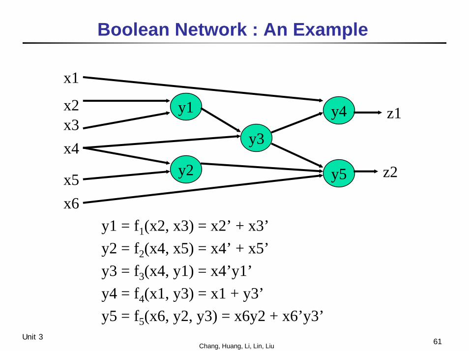
61Chang, Huang, Li, Lin, LiuUnit 3
Boolean Network : An Example
x1
y1
y2
y3
y4
y5
x2 z1x3x4
z2x5x6
y1 = f1(x2, x3) = x2’ + x3’y2 = f2(x4, x5) = x4’ + x5’y3 = f3(x4, y1) = x4’y1’y4 = f4(x1, y3) = x1 + y3’y5 = f5(x6, y2, y3) = x6y2 + x6’y3’

62Chang, Huang, Li, Lin, LiuUnit 3
Multi-Level v.s. Two-Level
․Two-level:⎯ Often used in control logic
designf1 = x1x2 + x1x3 + x1x4
f2 = x1’x2 + x1’x3 + x1x4
⎯ Only x1x4 shared⎯ Sharing restricted to
common cube
․Multi-level:⎯ Datapath or control logic
design⎯ Can share x2 + x3 between
the two expressions⎯ Can use complex gates
g1 = x2 + x3
g2 = x2x4
f1 = x1y1 + y2
f2 = x1’y1 + y2
(yi is the output of gate gi )
63Chang, Huang, Li, Lin, LiuUnit 3
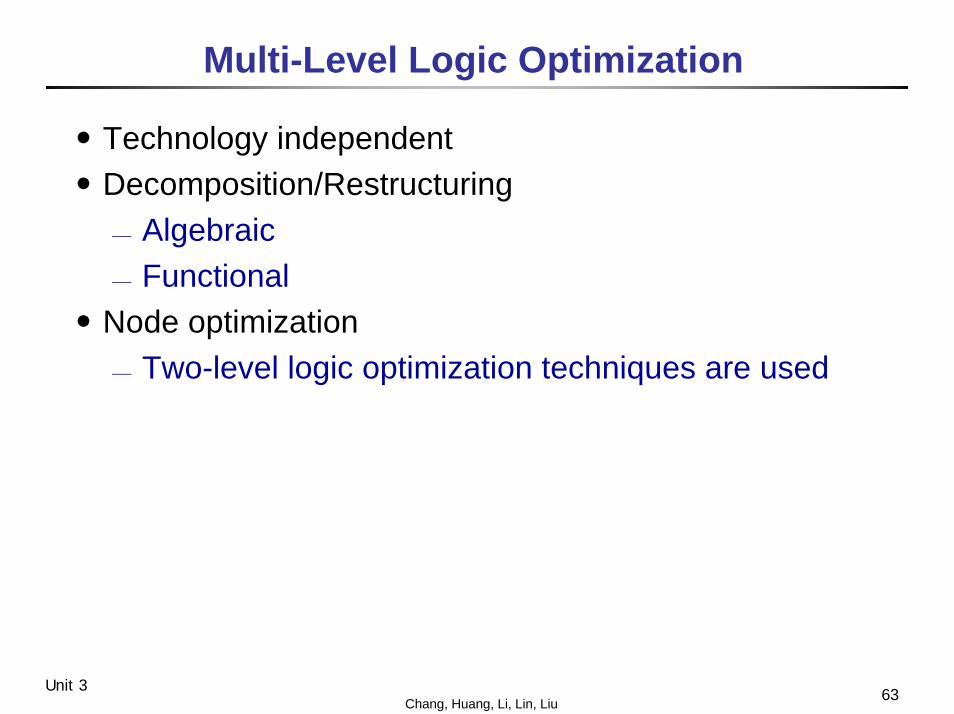
Multi-Level Logic Optimization
․Technology independent․Decomposition/Restructuring
⎯ Algebraic⎯ Functional
․Node optimization⎯ Two-level logic optimization techniques are used
64Chang, Huang, Li, Lin, LiuUnit 3
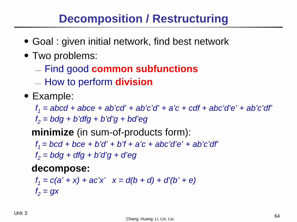
Decomposition / Restructuring
․Goal : given initial network, find best network․Two problems:
⎯ Find good common subfunctions⎯ How to perform division
․Example:f1 = abcd + abce + ab’cd’ + ab’c’d’ + a’c + cdf + abc’d’e’ + ab’c’df’f2 = bdg + b’dfg + b’d’g + bd’eg
minimize (in sum-of-products form):f1 = bcd + bce + b’d’ + b’f + a’c + abc’d’e’ + ab’c’df’f2 = bdg + dfg + b’d’g + d’eg
decompose:f1 = c(a’ + x) + ac’x’ x = d(b + d) + d’(b’ + e)f2 = gx
65Chang, Huang, Li, Lin, LiuUnit 3
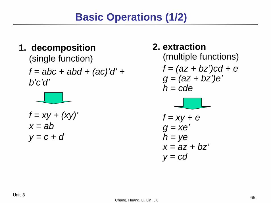
Basic Operations (1/2)
2. extraction(multiple functions)f = (az + bz’)cd + eg = (az + bz’)e’h = cde
f = xy + eg = xe’h = yex = az + bz’y = cd
1. decomposition(single function)f = abc + abd + (ac)’d’ + b’c’d’
f = xy + (xy)’x = aby = c + d
66Chang, Huang, Li, Lin, LiuUnit 3
Basic Operations (2/2)
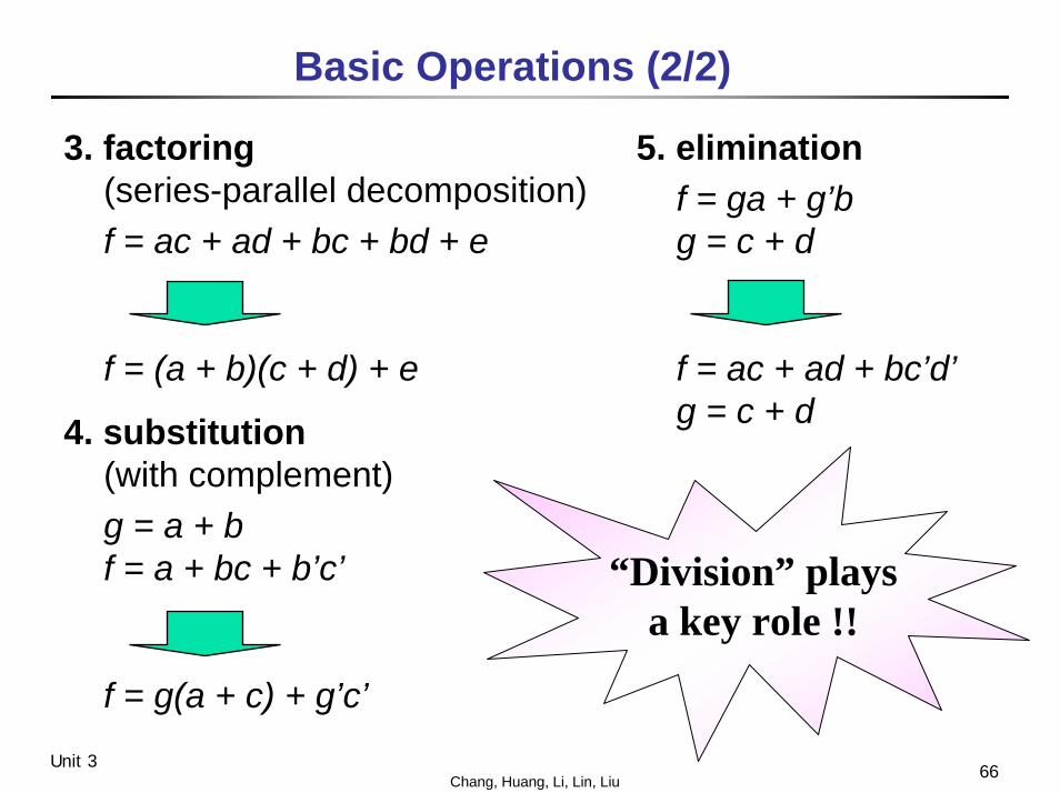
5. eliminationf = ga + g’bg = c + d
f = ac + ad + bc’d’g = c + d
3. factoring(series-parallel decomposition)f = ac + ad + bc + bd + e
f = (a + b)(c + d) + e
4. substitution(with complement)g = a + bf = a + bc + b’c’
f = g(a + c) + g’c’
“Division” playsa key role !!

67Chang, Huang, Li, Lin, LiuUnit 3
Division
․Division: p is a Boolean divisor of f if q ≠ φ and r exist such that f = pq + r⎯ p is said to be a factor of f if in addition r = φ :
f = pq⎯ q is called the quotient⎯ r is called the remainder⎯ q and r are not unique
․Weak division: the unique algebraic division such that r has as few cubes as possible⎯ The quotient q resulting from weak division is denoted by f / p
(it is unique)
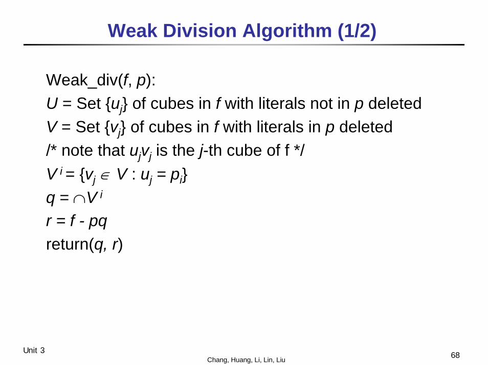
68Chang, Huang, Li, Lin, LiuUnit 3
Weak Division Algorithm (1/2)
Weak_div(f, p):U = Set {uj} of cubes in f with literals not in p deletedV = Set {vj} of cubes in f with literals in p deleted/* note that ujvj is the j-th cube of f */V i = {vj ∈ V : uj = pi}q = ∩V i
r = f - pqreturn(q, r)

69Chang, Huang, Li, Lin, LiuUnit 3
Weak Division Algorithm (2/2)
․Examplef = acg + adg + ae + bc + bd + be + a’bp = ag + bU = ag + ag + a + b + b + b + bV = c + d + e + c + d + e + a’Vag = c + dVb = c + d + e + a’q = c + d = f/p
commonexpressions
70Chang, Huang, Li, Lin, LiuUnit 3
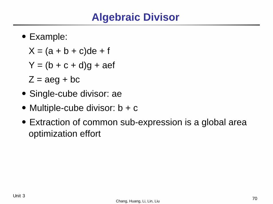
Algebraic Divisor
․Example:X = (a + b + c)de + fY = (b + c + d)g + aefZ = aeg + bc
․Single-cube divisor: ae․Multiple-cube divisor: b + c․Extraction of common sub-expression is a global area
optimization effort
71Chang, Huang, Li, Lin, LiuUnit 3
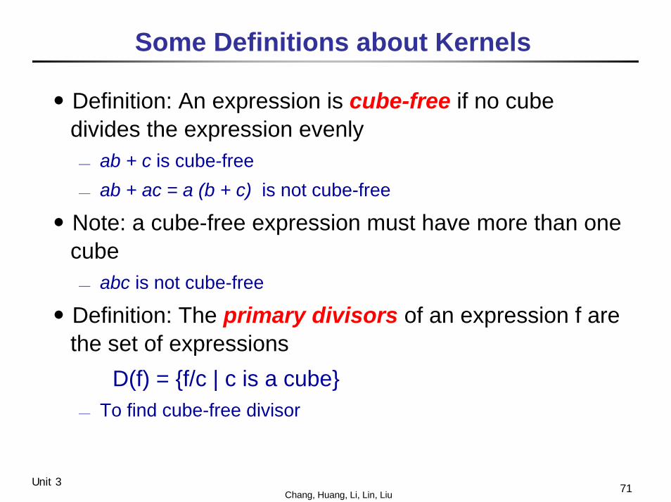
Some Definitions about Kernels
․Definition: An expression is cube-free if no cube divides the expression evenly⎯ ab + c is cube-free⎯ ab + ac = a (b + c) is not cube-free
․Note: a cube-free expression must have more than one cube⎯ abc is not cube-free
․Definition: The primary divisors of an expression f are the set of expressions
D(f) = {f/c | c is a cube}⎯ To find cube-free divisor

72Chang, Huang, Li, Lin, LiuUnit 3
Kernels
․Definition: The kernels of an expression f are the set of expressions
K(f) = {g | g∈ D(f) and g is cube free}․The kernels of an expression f are K(f) = {f/c}, where
⎯ / denote algebraic polynomial division⎯ c is a cube⎯ No cube divide f/c evenly (without any remainder)
․The cube c used to obtain the kernel is the co-kernelfor that kernel
73Chang, Huang, Li, Lin, LiuUnit 3
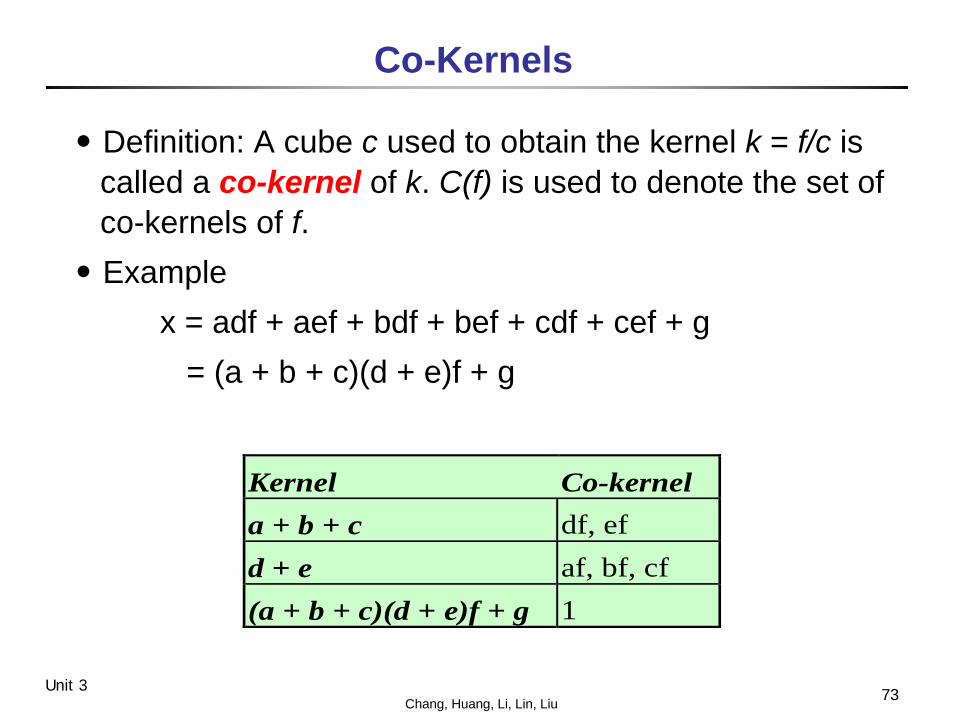
Co-Kernels
․Definition: A cube c used to obtain the kernel k = f/c is called a co-kernel of k. C(f) is used to denote the set of co-kernels of f.
․Examplex = adf + aef + bdf + bef + cdf + cef + g
= (a + b + c)(d + e)f + g
Kernel Co-kernel a + b + c df, ef d + e af, bf, cf (a + b + c)(d + e)f + g 1
74Chang, Huang, Li, Lin, LiuUnit 3
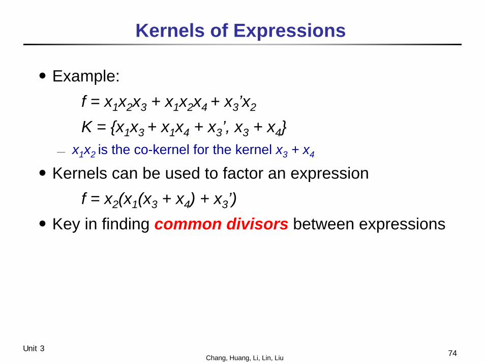
Kernels of Expressions
․Example:f = x1x2x3 + x1x2x4 + x3’x2
K = {x1x3 + x1x4 + x3’, x3 + x4}⎯ x1x2 is the co-kernel for the kernel x3 + x4
․Kernels can be used to factor an expressionf = x2(x1(x3 + x4) + x3’)
․Key in finding common divisors between expressions
75Chang, Huang, Li, Lin, LiuUnit 3
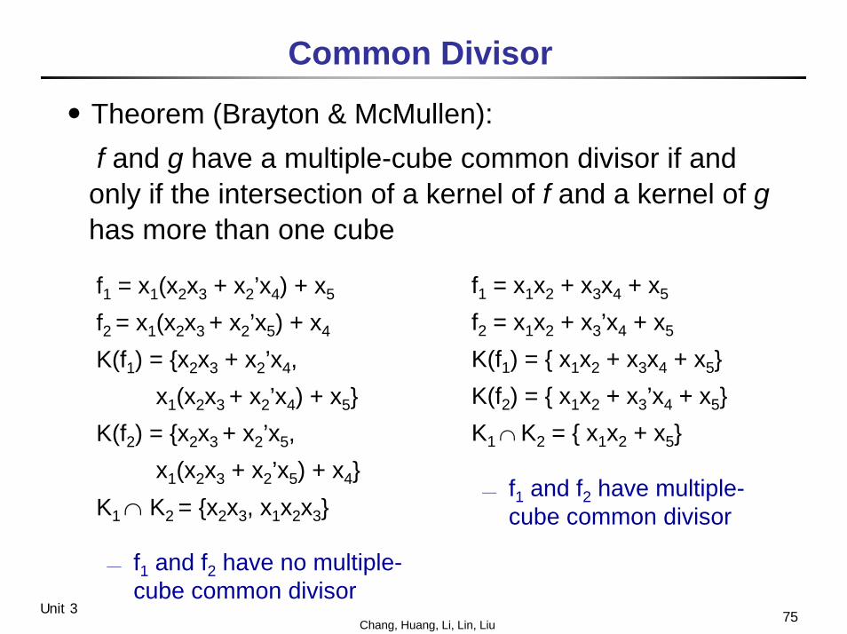
Common Divisor
․Theorem (Brayton & McMullen):f and g have a multiple-cube common divisor if and only if the intersection of a kernel of f and a kernel of ghas more than one cube
f1 = x1x2 + x3x4 + x5
f2 = x1x2 + x3’x4 + x5
K(f1) = { x1x2 + x3x4 + x5}K(f2) = { x1x2 + x3’x4 + x5}K1 ∩K2 = { x1x2 + x5}
⎯ f1 and f2 have multiple-cube common divisor
f1 = x1(x2x3 + x2’x4) + x5
f2 = x1(x2x3 + x2’x5) + x4
K(f1) = {x2x3 + x2’x4,x1(x2x3 + x2’x4) + x5}
K(f2) = {x2x3 + x2’x5,x1(x2x3 + x2’x5) + x4}
K1 ∩ K2 = {x2x3, x1x2x3}
⎯ f1 and f2 have no multiple-cube common divisor
76Chang, Huang, Li, Lin, LiuUnit 3
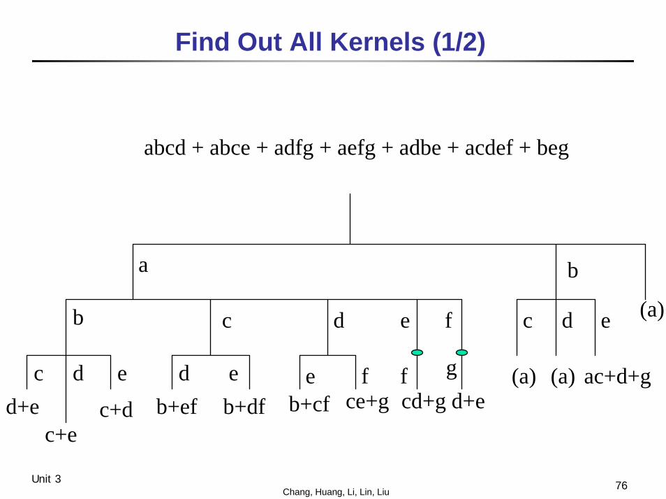
Find Out All Kernels (1/2)
abcd + abce + adfg + aefg + adbe + acdef + beg
a b
d+ec+e
c db+cf ce+g
e f f g
c+de d e
b+ef b+df
e f
cd+g d+e
(a)b c d c d e
(a) (a) ac+d+g

77Chang, Huang, Li, Lin, LiuUnit 3
Find Out All Kernels (2/2)
co-kernel kernel 1 a((bc + fg)(d + e) + de(b + cf))) + beg a (bc + fg)(d + e) + de(b + cf) ab c(d + e) + de abc d + e . . ac b(d + e) + def acd b + ef . . bc ad + ae
They can be obtained in n2 timewhere n is number of cubes in this expression.

78Chang, Huang, Li, Lin, LiuUnit 3
Cube-Literal Matrix
․Cube-literal matrixf = x1x2x3x4x7 + x1x2x3x4x8 + x1x2x3x5 + x1x2x3x6 + x1x2x9
x1 x2 x3 x4 x5 x6 x7 x8 x9 x1x2x3x4x7 1 1 1 1 0 0 1 0 0 x1x2x3x4x8 1 1 1 1 0 0 0 1 0 x1x2x3x5 1 1 1 0 1 0 0 0 0 x1x2x3x6 1 1 1 0 0 1 0 0 0 x1x2x9 1 1 0 0 0 0 0 0 1
79Chang, Huang, Li, Lin, LiuUnit 3
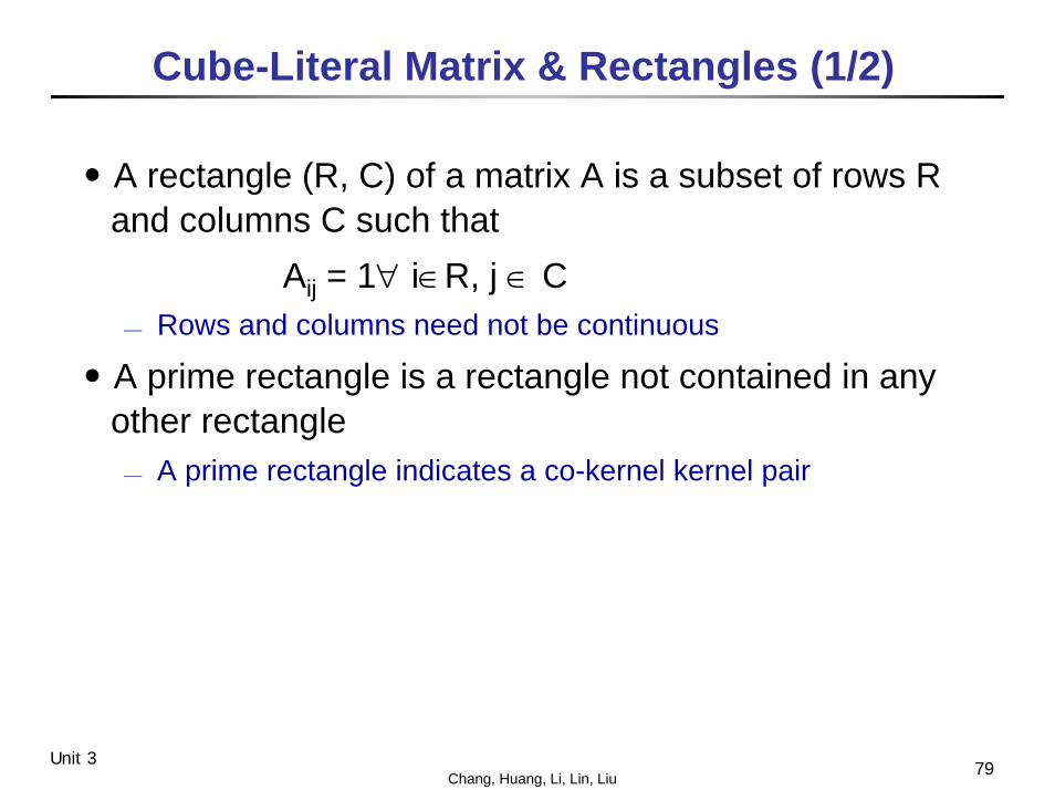
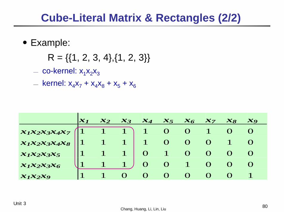
Cube-Literal Matrix & Rectangles (1/2)
․A rectangle (R, C) of a matrix A is a subset of rows R and columns C such that
Aij = 1∀ i∈R, j ∈ C⎯ Rows and columns need not be continuous
․A prime rectangle is a rectangle not contained in any other rectangle⎯ A prime rectangle indicates a co-kernel kernel pair
80Chang, Huang, Li, Lin, LiuUnit 3
Cube-Literal Matrix & Rectangles (2/2)
․Example:R = {{1, 2, 3, 4},{1, 2, 3}}
⎯ co-kernel: x1x2x3
⎯ kernel: x4x7 + x4x8 + x5 + x6
x1 x2 x3 x4 x5 x6 x7 x8 x9 x1x2x3x4x7 1 1 1 1 0 0 1 0 0 x1x2x3x4x8 1 1 1 1 0 0 0 1 0 x1x2x3x5 1 1 1 0 1 0 0 0 0 x1x2x3x6 1 1 1 0 0 1 0 0 0 x1x2x9 1 1 0 0 0 0 0 0 1
81Chang, Huang, Li, Lin, LiuUnit 3
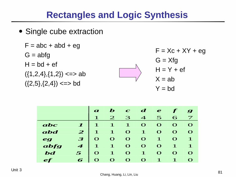
Rectangles and Logic Synthesis
․Single cube extraction
F = abc + abd + egG = abfgH = bd + ef({1,2,4},{1,2}) <=> ab({2,5},{2,4}) <=> bd
F = Xc + XY + egG = XfgH = Y + efX = abY = bd
a b c d e f g 1 2 3 4 5 6 7
abc 1 1 1 1 0 0 0 0abd 2 1 1 0 1 0 0 0eg 3 0 0 0 0 1 0 1abfg 4 1 1 0 0 0 1 1bd 5 0 1 0 1 0 0 0ef 6 0 0 0 0 1 1 0
82Chang, Huang, Li, Lin, LiuUnit 3
Outline
․Synthesis overview․RTL synthesis
⎯ Combinational circuit generation⎯ Special element inferences
․Logic optimization⎯ Two-level logic optimization⎯ Multi-level logic optimization
․Technology mapping․Timing optimization․Synthesis for low power․Retiming
83Chang, Huang, Li, Lin, LiuUnit 3
Technology Mapping
․General approach:⎯ Choose base function set for canonical representation
Ex: 2-input NAND and Inverter⎯ Represent optimized network using base functions
Subject graph⎯ Represent library cells using base functions
Pattern graph⎯ Each pattern associated with a cost which is dependent on the
optimization criteria
․Goal:⎯ Finding a minimal cost covering of a subject graph using
pattern graphs

84Chang, Huang, Li, Lin, LiuUnit 3
Example Pattern Graph (1/3)
inv (1)nor2 (2)
nand2 (1)
nand3 (3) nor3 (3)
nand4 (4) nor4 (4)
85Chang, Huang, Li, Lin, LiuUnit 3
Example Pattern Graph (2/3)
nand4 (4) nor4 (4)
aoi21 (3) oai21 (3)
oai22 (4)aoi22 (4)

86Chang, Huang, Li, Lin, LiuUnit 3
Example Pattern Graph (3/3)
and2 (3) or2 (3)
xor (5) xnor (5)

87Chang, Huang, Li, Lin, LiuUnit 3
Example Subject Graph
t1 = d + e;t2 = b + h;t3 = a t2 + c;t4 = t1 t3 + f g h;F = t4’;
fgdehbac
F

88Chang, Huang, Li, Lin, LiuUnit 3
Sample Covers (1/2)
fgdehbac
FOR2
OR2
AND2
AOI22
NAND2
NAND2INV
Area = 18

89Chang, Huang, Li, Lin, LiuUnit 3
Sample Covers (2/2)
Area = 15
OAI21
OAI21
NAND3
AND2
NAND2INV
fg
dehbac
F
90Chang, Huang, Li, Lin, LiuUnit 3
DAGON Approach․Partition a subject graph into trees
⎯ Cut the graph at all multiple fanout points
․Optimally cover each tree using dynamic programming approach
․Piece the tree-covers into a cover for the subject graph
91Chang, Huang, Li, Lin, LiuUnit 3
Dynamic Programming for Minimum Area
․Principle of optimality: optimal cover for the tree consists of a match at the root plus the optimal cover for the sub-tree starting at each input of the match
I1
I3
I2
I4
Match: area = m
root
A(root) = m + A(I1) + A(I2) + A(I3) + A(I4) cost of a leaf = 0
92Chang, Huang, Li, Lin, LiuUnit 3
A Library Example
INV 2 a’
NAND2 3 (ab)’
NAND3 4 (abc)’
NAND4 5 (abcd)’
AOI21 4 (ab+c)’
AOI22 5 (ab+cd)’
Library Element Canonical Form
93Chang, Huang, Li, Lin, LiuUnit 3
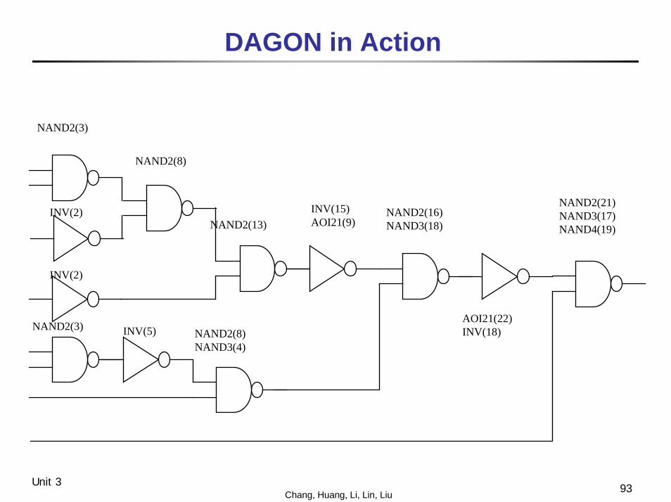
DAGON in Action
NAND2(3)
INV(2)
NAND2(8)
INV(2)
NAND2(3) INV(5) NAND2(8)NAND3(4)
NAND2(13)INV(15)AOI21(9)
NAND2(16)NAND3(18)
AOI21(22)INV(18)
NAND2(21)NAND3(17)NAND4(19)
94Chang, Huang, Li, Lin, LiuUnit 3
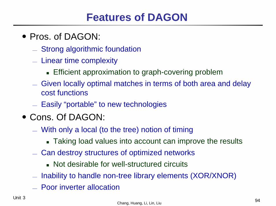
Features of DAGON
․Pros. of DAGON:⎯ Strong algorithmic foundation⎯ Linear time complexity
Efficient approximation to graph-covering problem⎯ Given locally optimal matches in terms of both area and delay
cost functions⎯ Easily “portable” to new technologies
․Cons. Of DAGON:⎯ With only a local (to the tree) notion of timing
Taking load values into account can improve the results⎯ Can destroy structures of optimized networks
Not desirable for well-structured circuits⎯ Inability to handle non-tree library elements (XOR/XNOR)⎯ Poor inverter allocation

95Chang, Huang, Li, Lin, LiuUnit 3
Inverter Allocation
․Add a pair of inverters for each wire in the subject graph
․Add a pattern of a wire that matches two inverters with zero cost
․Effect: may further improve the solution
2 INV1 AIO21
2 NOR2
96Chang, Huang, Li, Lin, LiuUnit 3
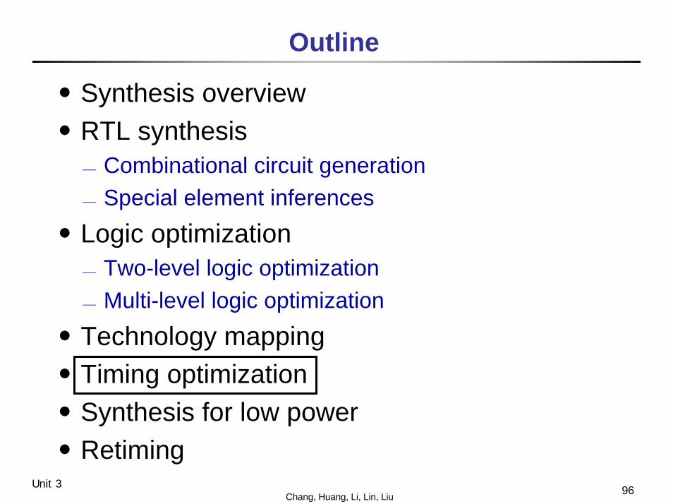
Outline
․Synthesis overview․RTL synthesis
⎯ Combinational circuit generation⎯ Special element inferences
․Logic optimization⎯ Two-level logic optimization⎯ Multi-level logic optimization
․Technology mapping․Timing optimization․Synthesis for low power․Retiming

97Chang, Huang, Li, Lin, LiuUnit 3
Delay Model at Logic Level
1. unit delay model⎯ Assign a delay of 1 to each gate
2. unit fanout delay model⎯ Incorporate an additional delay for each fanout
3. library delay model⎯ Use delay data in the library to provide more accurate delay value⎯ May use linear or non-linear (tabular) models
98Chang, Huang, Li, Lin, LiuUnit 3
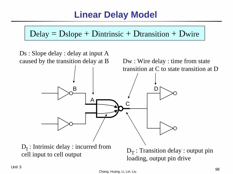
Linear Delay Model
Delay = Dslope + Dintrinsic + Dtransition + Dwire
B
AC
D
Ds : Slope delay : delay at input A caused by the transition delay at B Dw : Wire delay : time from state
transition at C to state transition at D
DI : Intrinsic delay : incurred from cell input to cell output DT : Transition delay : output pin
loading, output pin drive
99Chang, Huang, Li, Lin, LiuUnit 3
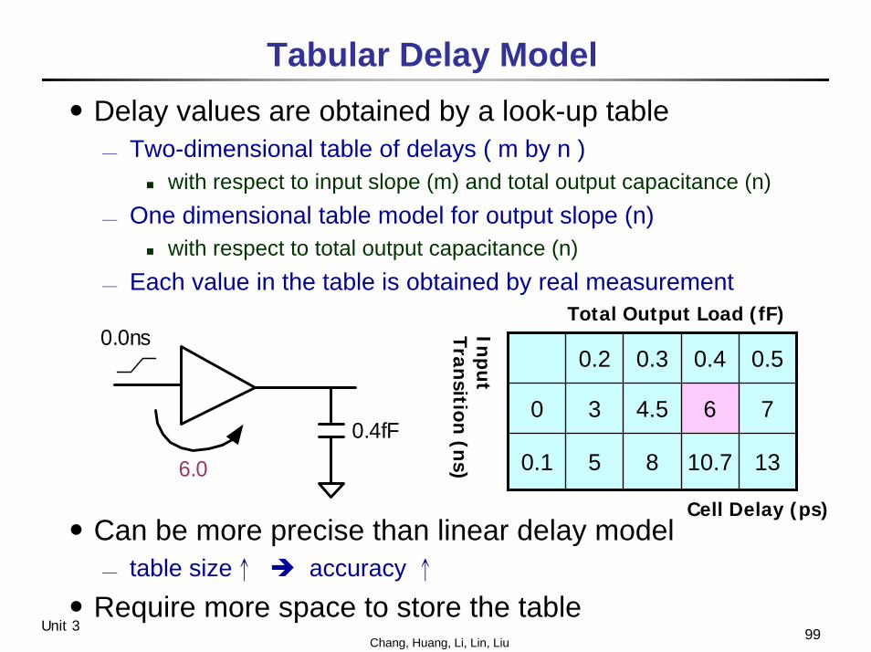
Tabular Delay Model․Delay values are obtained by a look-up table
⎯ Two-dimensional table of delays ( m by n )with respect to input slope (m) and total output capacitance (n)
⎯ One dimensional table model for output slope (n)with respect to total output capacitance (n)
⎯ Each value in the table is obtained by real measurement
․Can be more precise than linear delay model⎯ table size↑ accuracy ↑
․Require more space to store the table
0.0ns
0.4fF
6.0
0.2 0.3 0.4 0.5
0 3 4.5 6 7
0.1 5 8 10.7 13
Total Output Load (fF)
Inpu
tTran
sition (n
s)
Cell Delay (ps)

100Chang, Huang, Li, Lin, LiuUnit 3
Arrival Time and Required Time
․arrival time : calculated from input to output․required time : calculated from output to input․slack = required time - arrival time
node k
A(j) R(j)
node jD(j,k)
r(j,k)
A(k) R(k)
A(j): arrival time of signal jR(k): required time or for signal kS(k): slack of signal kD(j,k): delay of node j from input k
A(j) = maxk∈FI (j) [A(k) + D(j,k)]r(j,k) = R(j) - D(j,k)R(k) = minj∈FO(k) [r(j,k)]S(k) = R(k) - A(k)

101Chang, Huang, Li, Lin, LiuUnit 3
Delay Graph
․Replace logic gates with delay blocks․Add start (S) and end (E) blocks․Indicate signal flow with directed arcs
A
BC
DE
1
2
S E
102Chang, Huang, Li, Lin, LiuUnit 3
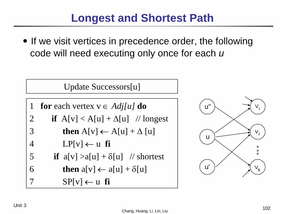
Longest and Shortest Path
․If we visit vertices in precedence order, the following code will need executing only once for each u
Update Successors[u]
V1
V2
Vk
u''
u
u'
1 for each vertex v ∈ Adj[u] do2 if A[v] < A[u] + ∆[u] // longest3 then A[v] ← A[u] + ∆ [u]4 LP[v] ← u fi5 if a[v] >a[u] + δ[u] // shortest6 then a[v] ← a[u] + δ[u]7 SP[v] ← u fi

103Chang, Huang, Li, Lin, LiuUnit 3
Delay Graph and Topological Sort
ES 5
1 2
6
9 10
7 8
3 4
1 5S 9 2 6 3 7 10 4 8 E
104Chang, Huang, Li, Lin, LiuUnit 3
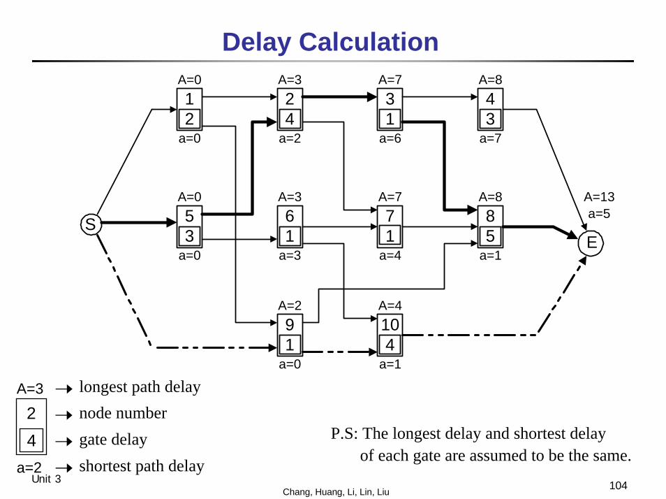
Delay Calculation
ES 5
3
12
24
61
91
104
71
85
31
43
A=3A=0 A=7 A=8
a=7
A=8
a=6a=2a=0
A=7A=3A=0
a=0 a=3 a=4 a=1
A=4
a=1
A=2
a=0
a=5A=13
longest path delay
4
A=3node number2
P.S: The longest delay and shortest delayof each gate are assumed to be the same.
gate delayshortest path delaya=2
105Chang, Huang, Li, Lin, LiuUnit 3
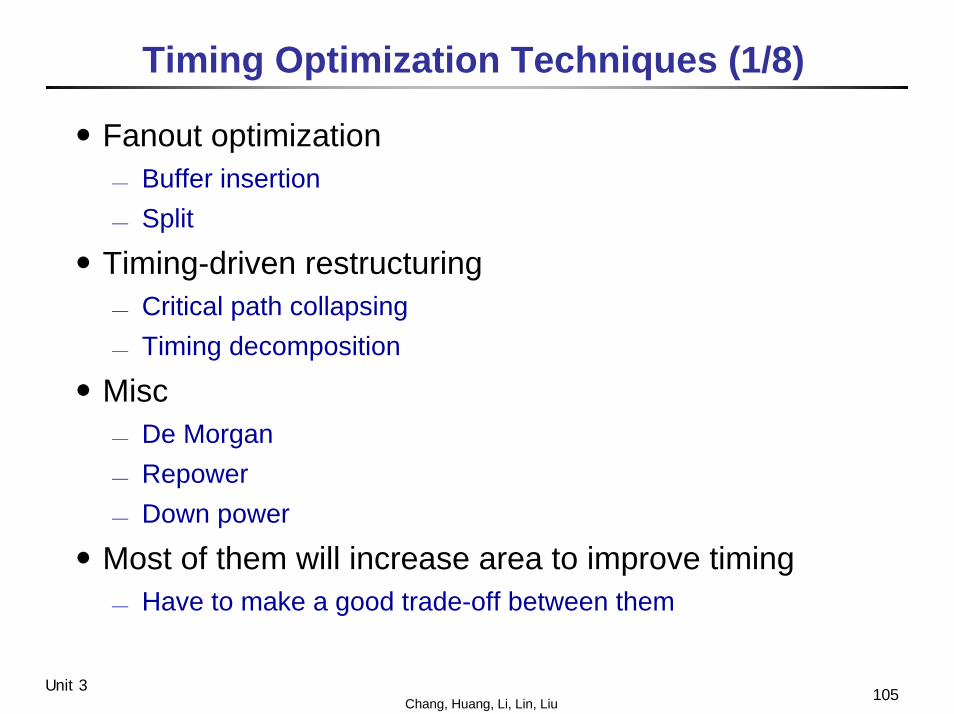
Timing Optimization Techniques (1/8)
․Fanout optimization⎯ Buffer insertion⎯ Split
․Timing-driven restructuring⎯ Critical path collapsing⎯ Timing decomposition
․Misc⎯ De Morgan⎯ Repower⎯ Down power
․Most of them will increase area to improve timing⎯ Have to make a good trade-off between them
106Chang, Huang, Li, Lin, LiuUnit 3
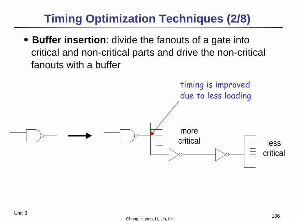
Timing Optimization Techniques (2/8)
․Buffer insertion: divide the fanouts of a gate into critical and non-critical parts and drive the non-critical fanouts with a buffer
morecritical less
critical
timing is improveddue to less loading
107Chang, Huang, Li, Lin, LiuUnit 3
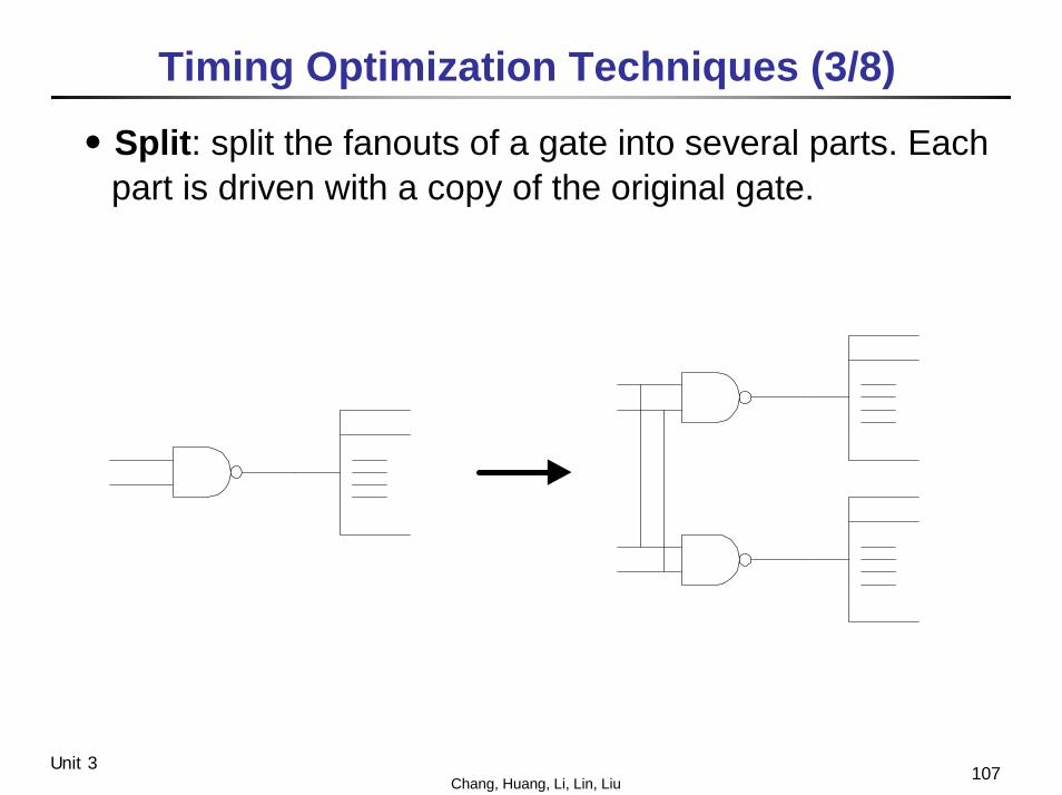
Timing Optimization Techniques (3/8)
․Split: split the fanouts of a gate into several parts. Each part is driven with a copy of the original gate.
108Chang, Huang, Li, Lin, LiuUnit 3
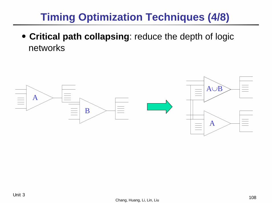
Timing Optimization Techniques (4/8)
․Critical path collapsing: reduce the depth of logic networks
A
B
A
A∪B
109Chang, Huang, Li, Lin, LiuUnit 3
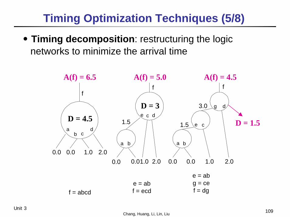
Timing Optimization Techniques (5/8)
․Timing decomposition: restructuring the logic networks to minimize the arrival time
ff f
1.5
3.0
1.5
0.0 0.0 1.0 2.00.0 0.01.0 2.0 2.01.00.0 0.0
f = abcde = abf = ecd
e = abg = cef = dg
ab c
d
e
g
d
e
a b
c
a b
c
d
A(f) = 6.5 A(f) = 5.0 A(f) = 4.5
D = 4.5D = 3
D = 1.5
110Chang, Huang, Li, Lin, LiuUnit 3
Timing Optimization Techniques (6/8)
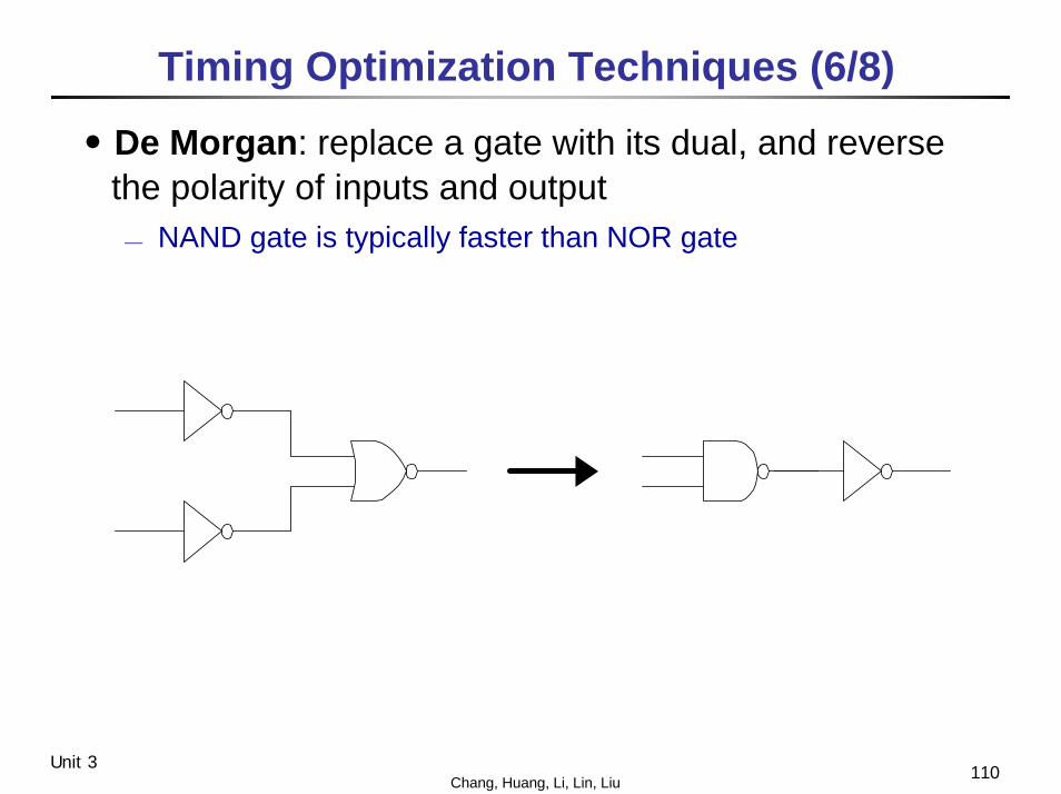
․De Morgan: replace a gate with its dual, and reverse the polarity of inputs and output⎯ NAND gate is typically faster than NOR gate
111Chang, Huang, Li, Lin, LiuUnit 3
Timing Optimization Techniques (7/8)
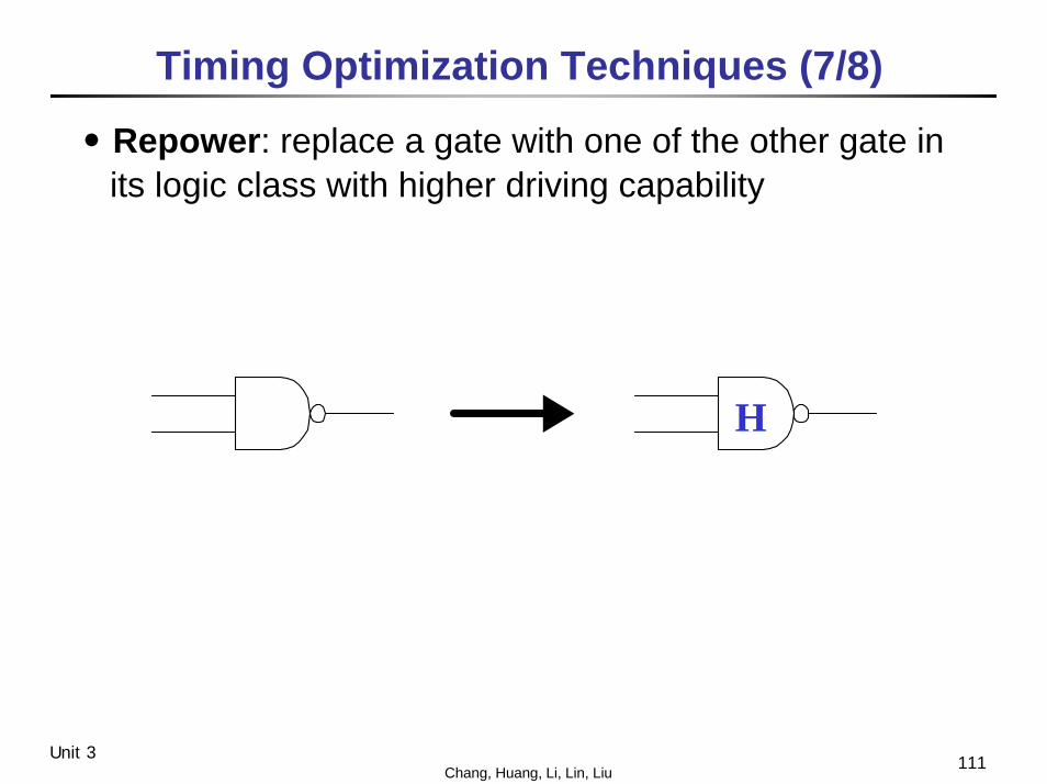
․Repower: replace a gate with one of the other gate in its logic class with higher driving capability
H

112Chang, Huang, Li, Lin, LiuUnit 3
Timing Optimization Techniques (8/8)
․Down power: reducing gate size of a non-critical fanoutin the critical path
notcritical
critical
H
113Chang, Huang, Li, Lin, LiuUnit 3
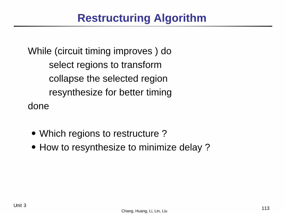
Restructuring Algorithm
While (circuit timing improves ) doselect regions to transformcollapse the selected regionresynthesize for better timing
done
․Which regions to restructure ?․How to resynthesize to minimize delay ?
114Chang, Huang, Li, Lin, LiuUnit 3
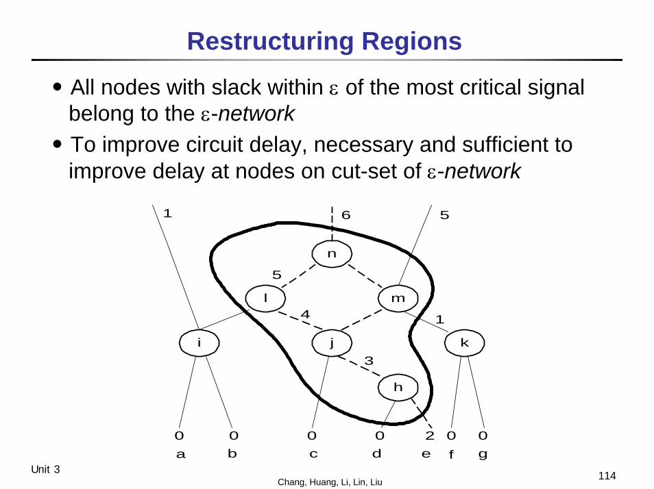
Restructuring Regions
․All nodes with slack within ε of the most critical signal belong to the ε-network
․To improve circuit delay, necessary and sufficient to improve delay at nodes on cut-set of ε-network
ki
n
l
j
m
h
0 0 0 00 02a b c d e f g
1 6 5
5
4 1
3

115Chang, Huang, Li, Lin, LiuUnit 3
Find the Cutset
․The weight of each node is W = Wxt + α * Wxa⎯ Wxt is potential for speedup⎯ Wxa is area penalty for duplication of logic⎯ α is decided by various area/delay tradeoff
․Apply the maxflow-mincut algorithm to generate the cutset of the ε-network

116Chang, Huang, Li, Lin, LiuUnit 3
Controlling the Algorithm
․ε: Specify the size of the ε-network⎯ Large ε might waste area without much reduction in critical
delay⎯ Small ε might slow down the algorithm
․d: The depth of the d-critical-fanin-section⎯ Large d might make large change in the delay⎯ Large d might increase run time rapidly due to the collapsing
effort and the large number of divisor
․α: Control the tradeoff between area and speed⎯ Large α avoids the duplication of logic⎯ α = 0 implies a speedup irrespective of the increase in area

117Chang, Huang, Li, Lin, LiuUnit 3
Outline
․Synthesis overview․RTL synthesis
⎯ Combinational circuit generation⎯ Special element inferences
․Logic optimization⎯ Two-level logic optimization⎯ Multi-level logic optimization
․Technology mapping․Timing optimization․Synthesis for low power․Retiming

118Chang, Huang, Li, Lin, LiuUnit 3
Power Dissipation
․Leakage power⎯ Static dissipation due to leakage current⎯ Typically a smaller value compared to other power dissipation⎯ Getting larger and larger in deep-submicron process
․Short-circuit power⎯ Due to the short-circuit current when both PMOS and NMOS
are open during transition⎯ Typically a smaller value compared to dynamic power
․Dynamic power⎯ Charge and discharge of a load capacitor⎯ Usually the major part of total
power consumption Vin
VDD
GND
Vout

119Chang, Huang, Li, Lin, LiuUnit 3
Power Dissipation Model
DVCP dd •••= 2
21
․Typically, dynamic power is used to represent total power dissipationP: the power dissipation for a gateC: the load capacitanceVdd: the supply voltageD: the transition density
․To obtain the power dissipation of the circuit, we need⎯ The node capacitance of each node (obtained from layout)⎯ The transition density of each node (obtained by computation)
120Chang, Huang, Li, Lin, LiuUnit 3
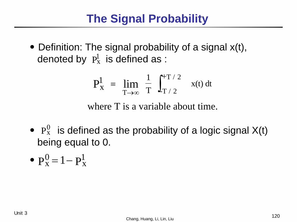
The Signal Probability
․Definition: The signal probability of a signal x(t), denoted by is defined as :
․ is defined as the probability of a logic signal X(t) being equal to 0.
․
where T is a variable about time.
xP1
x1
1T
x(t) dt+
P limT -T / 2
T / 2≡
→∞∫
x0P
x0
x1P P= −1
121Chang, Huang, Li, Lin, LiuUnit 3
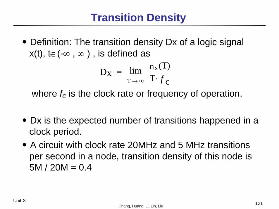
Transition Density
․Definition: The transition density Dx of a logic signal x(t), t∈(-∞ , ∞ ) , is defined as
where fc is the clock rate or frequency of operation.
․Dx is the expected number of transitions happened in a clock period.
․A circuit with clock rate 20MHz and 5 MHz transitions per second in a node, transition density of this node is 5M / 20M = 0.4
xD lim n (T)T cT
x≡⋅→ ∞ f

122Chang, Huang, Li, Lin, LiuUnit 3
Signal Probability and Transition Density
Clock
Signal a
Signal b
Signal c
Signal d
Pa = 0.5 Da = 1
Pb = 0.5 Db = 0.5
Pc = 0.5 Dc = 0.25
Pd = 0.25 Dd = 0.25
123Chang, Huang, Li, Lin, LiuUnit 3
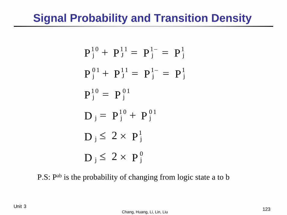
Signal Probability and Transition Density
j1 0
J1 1
j j1
j0 1
J1 1
j j1
j1 0
j0 1
j j1 0
j0 1
j j
j j
P P P P
P P P P
P P
D P P
D P
D P
+ = =
+ = =
=
= +
≤ ×
≤ ×
−
−
1
1
1
0
2
2
P.S: Pab is the probability of changing from logic state a to b

124Chang, Huang, Li, Lin, LiuUnit 3
The Calculation of Signal Probability․BDD-based approach is one of the popular way․Definition
⎯ p(F) : fraction of variable assignments for which F = 1
․Recursive Formulation⎯ p(F) = [ p( F[x=1] ) + p( F[x=0] ) ] / 2
․Computation⎯ Compute bottom-up, starting at leaves⎯ At each node, average the value of children
․Ex: F = d2’(d1+d0)a1a0 + d2(d1’+d0’)a1a0’+ d2d1d0a1’a0
p(F) = 7/32 = 0.21875
d2
d1 d1
a1 a1
d0 d0
1 0
a1
a0 a0
7/321/43/16
1/41/8
1/4 1/4 1/4
1/2
1/2
: 1
: 0
125Chang, Huang, Li, Lin, LiuUnit 3
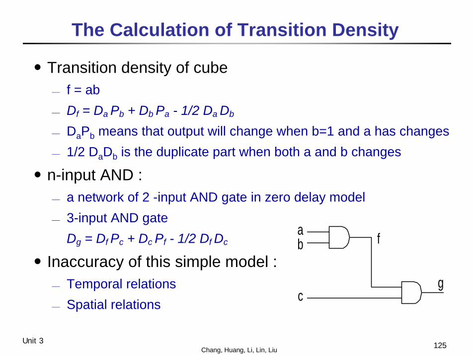
The Calculation of Transition Density
․Transition density of cube⎯ f = ab⎯ Df = Da Pb + Db Pa - 1/2 Da Db
⎯ DaPb means that output will change when b=1 and a has changes⎯ 1/2 DaDb is the duplicate part when both a and b changes
․n-input AND :⎯ a network of 2 -input AND gate in zero delay model ⎯ 3-input AND gate
Dg = Df Pc + Dc Pf - 1/2 Df Dc
․Inaccuracy of this simple model :⎯ Temporal relations ⎯ Spatial relations
ab
c
f
g
126Chang, Huang, Li, Lin, LiuUnit 3
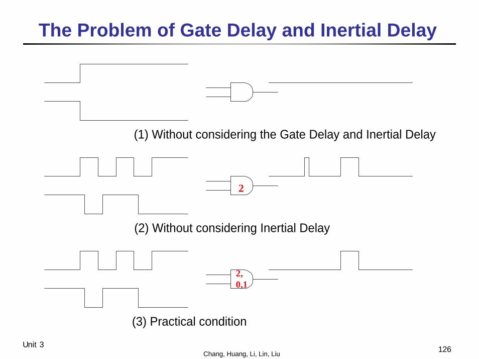
The Problem of Gate Delay and Inertial Delay
(1) Without considering the Gate Delay and Inertial Delay
(2) Without considering Inertial Delay
(3) Practical condition
2
2,0,1

127Chang, Huang, Li, Lin, LiuUnit 3
The Problem of Spatial Correlation
P = 0.5
P = 1-0.5 = 0.5
P = 0.5 * 0.5 = 0.25
P = 0.5
P = 1-0.5 = 0.5
P = 0
(a) Without considering Spatial Correlation
(b) Practical condition
128Chang, Huang, Li, Lin, LiuUnit 3
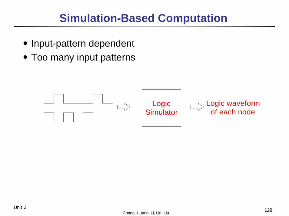
Simulation-Based Computation
․Input-pattern dependent․Too many input patterns
LogicSimulator
Logic waveformof each node

129Chang, Huang, Li, Lin, LiuUnit 3
Logic Minimization for Low Power (1/2)
․Consider an example:
․Different choices of the covers may result in different power consumption
abc 00 01 11 10
0
1
1
1 1 1
1 1
00 01 11 10abc
0
1
1
1 1
1
1
1
f = a'b' + ac' + bc f = b'c' + a'c + abP = 108.7 µW P = 115.5 µW
(a) (b)
f
a
b
c
c
b
a
f
130Chang, Huang, Li, Lin, LiuUnit 3
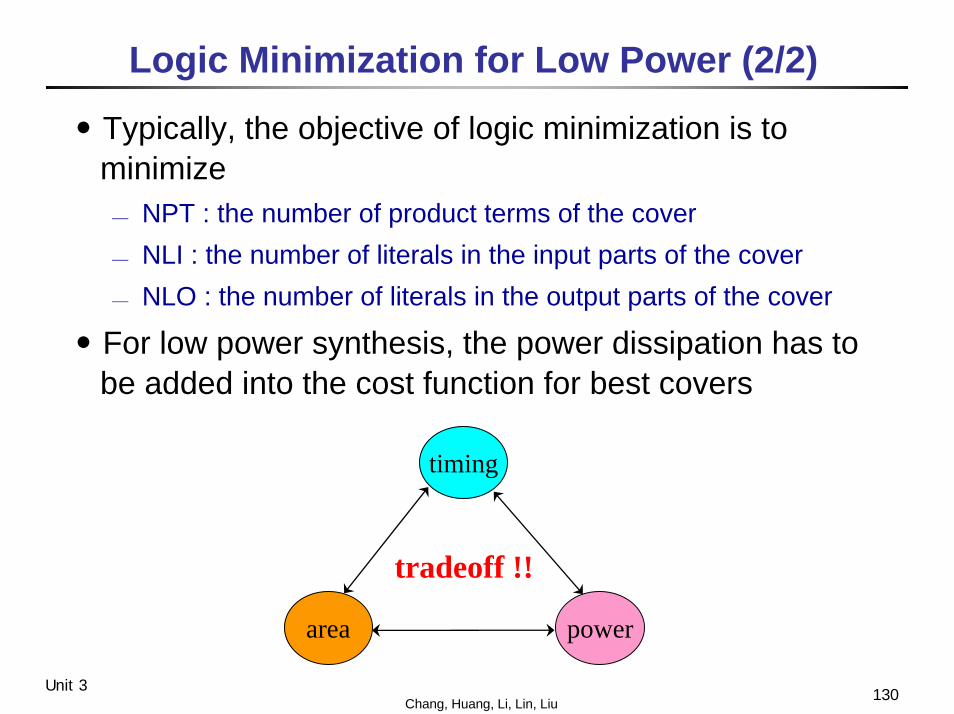
Logic Minimization for Low Power (2/2)
․Typically, the objective of logic minimization is to minimize⎯ NPT : the number of product terms of the cover⎯ NLI : the number of literals in the input parts of the cover⎯ NLO : the number of literals in the output parts of the cover
․For low power synthesis, the power dissipation has to be added into the cost function for best covers
timing
area power
tradeoff !!
131Chang, Huang, Li, Lin, LiuUnit 3
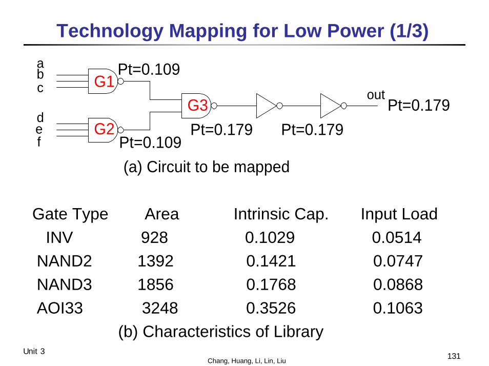
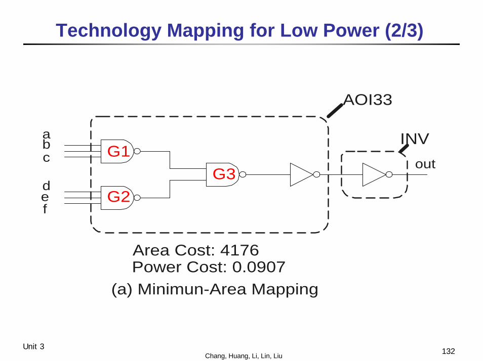
Technology Mapping for Low Power (1/3)abc
def
outG1
G2G3
(a) Circuit to be mapped
Pt=0.109
Pt=0.109Pt=0.179 Pt=0.179
Pt=0.179
Gate Type Area Intrinsic Cap. Input LoadINV 928 0.1029 0.0514
NAND2 1392 0.1421 0.0747NAND3 1856 0.1768 0.0868AOI33 3248 0.3526 0.1063
(b) Characteristics of Library
132Chang, Huang, Li, Lin, LiuUnit 3
Technology Mapping for Low Power (2/3)
abc
def
out
AOI33
INVG1
G2G3
Power Cost: 0.0907(a) Minimun-Area Mapping
Area Cost: 4176
133Chang, Huang, Li, Lin, LiuUnit 3
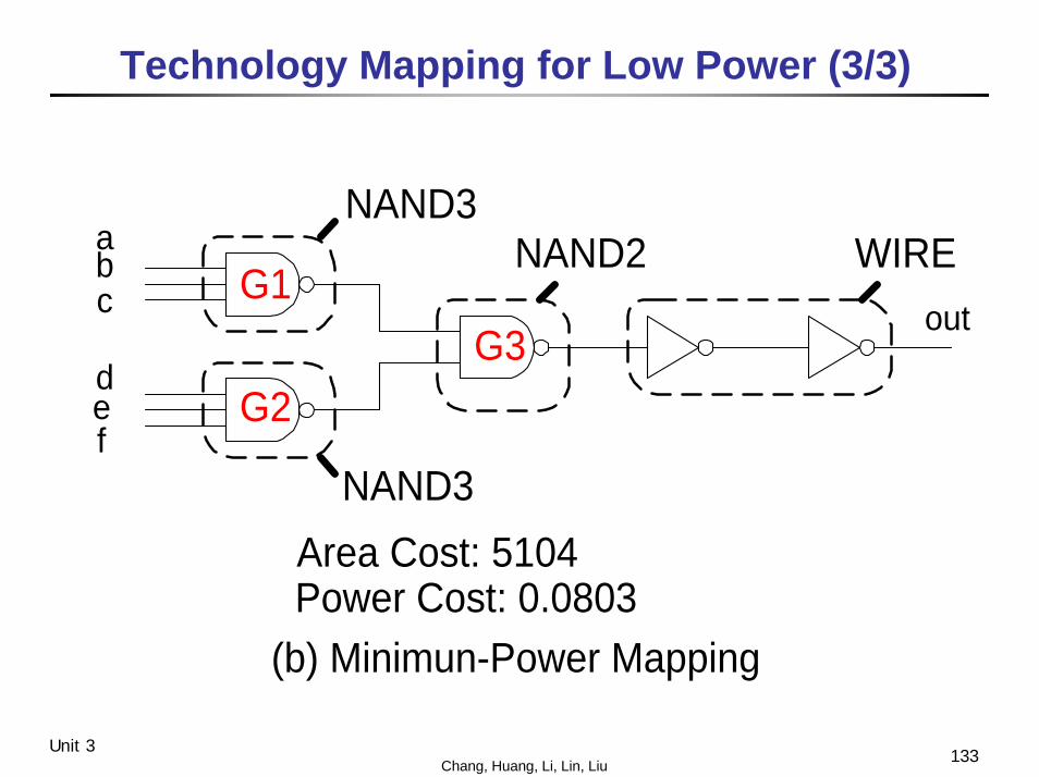
Technology Mapping for Low Power (3/3)
abc
def
outG1
G2G3
Power Cost: 0.0803(b) Minimun-Power Mapping
Area Cost: 5104
WIRENAND3
NAND3
NAND2

134Chang, Huang, Li, Lin, LiuUnit 3
Outline
․Synthesis overview․RTL synthesis
⎯ Combinational circuit generation⎯ Special element inferences
․Logic optimization⎯ Two-level logic optimization⎯ Multi-level logic optimization
․Technology mapping․Timing optimization․Synthesis for low power․Retiming
135Chang, Huang, Li, Lin, LiuUnit 3
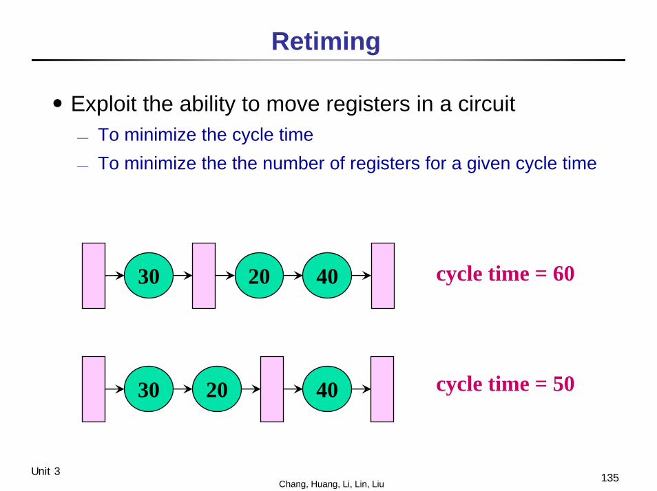
Retiming
․Exploit the ability to move registers in a circuit⎯ To minimize the cycle time⎯ To minimize the the number of registers for a given cycle time
30 20 40 cycle time = 60
30 20 40 cycle time = 50
136Chang, Huang, Li, Lin, LiuUnit 3
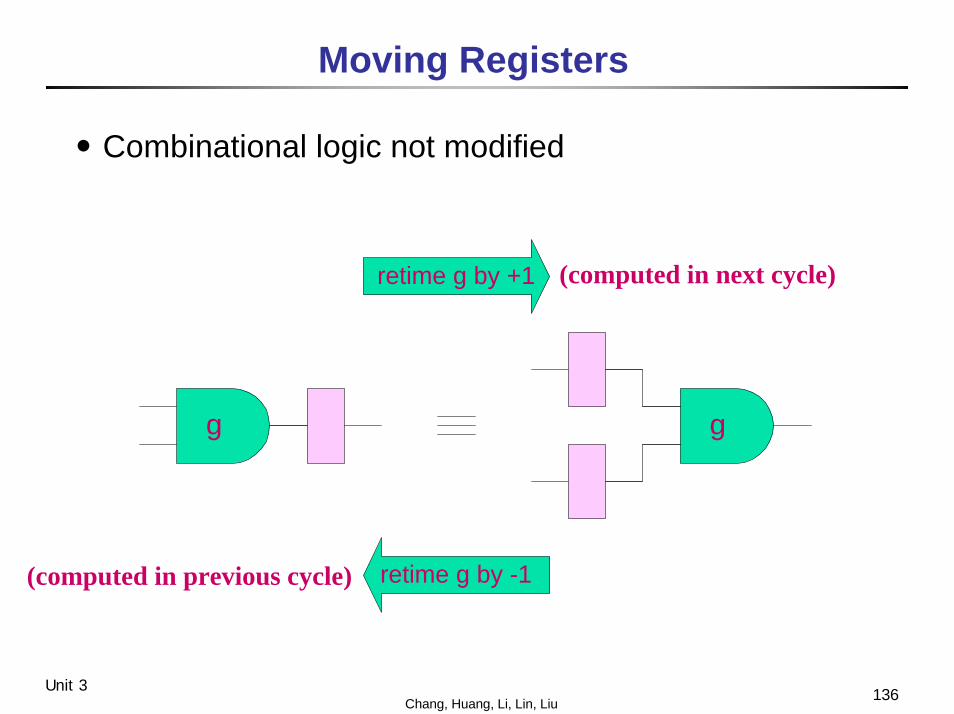
Moving Registers
․Combinational logic not modified
retime g by +1
retime g by -1
g g
(computed in next cycle)
(computed in previous cycle)

137Chang, Huang, Li, Lin, LiuUnit 3
Formulation
․Directed graph:⎯ Nodes: combinational logic⎯ Edges: connections (possible latched) between logic
․Weights⎯ Nodes: combinational logic propagation delay⎯ Edges: number of registers
․Path delay d(P): sum of node delays along a path․Path weight w(P): sum of edge weights along a path․Clock period: Φ(G) = max{d(p) | w(p) = 0}
138Chang, Huang, Li, Lin, LiuUnit 3
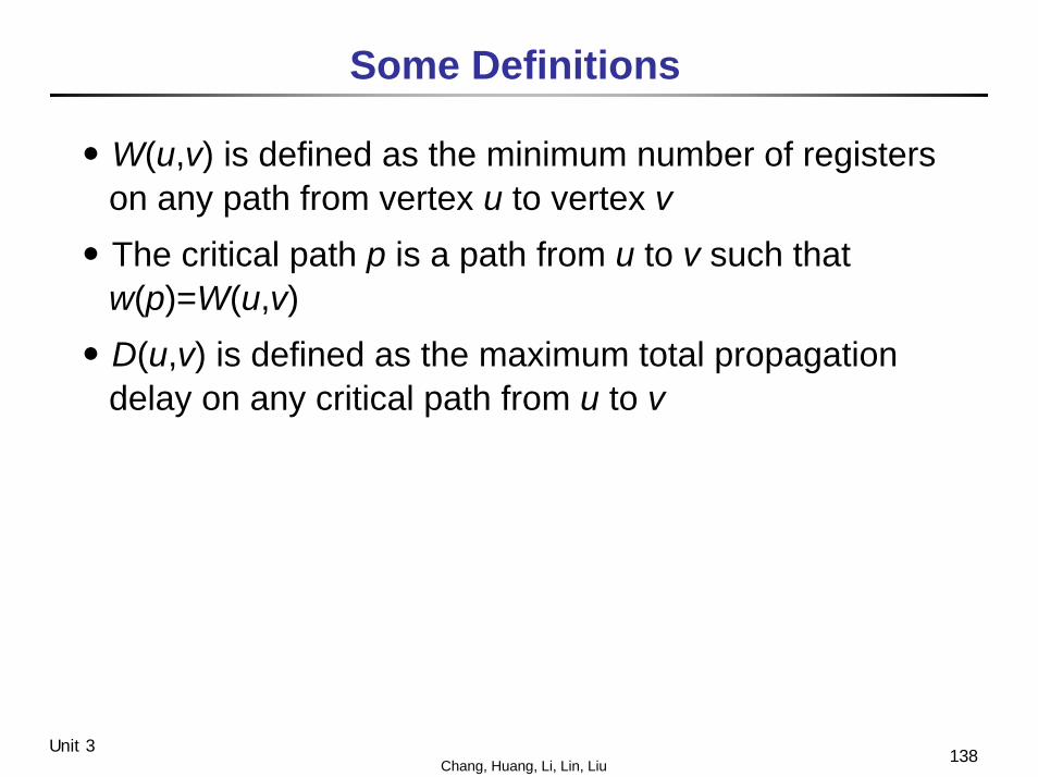
Some Definitions
․W(u,v) is defined as the minimum number of registers on any path from vertex u to vertex v
․The critical path p is a path from u to v such that w(p)=W(u,v)
․D(u,v) is defined as the maximum total propagation delay on any critical path from u to v

139Chang, Huang, Li, Lin, LiuUnit 3
Synchronous Circuits
A synchronous circuit must satisfy following rules:․D1: The propagation delay d(v) is non-negative for
each vertex v⎯ Infeasible in real cases
․W1: The register count w(e) is non-negative for each edge e⎯ Infeasible in real cases
․W2: In any directed cycle, there is some edge with positive register count⎯ No combinational loops
140Chang, Huang, Li, Lin, LiuUnit 3
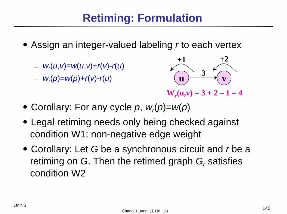
Retiming: Formulation
․Assign an integer-valued labeling r to each vertex
⎯ wr(u,v)=w(u,v)+r(v)-r(u)⎯ wr(p)=w(p)+r(v)-r(u)
․Corollary: For any cycle p, wr(p)=w(p)․Legal retiming needs only being checked against
condition W1: non-negative edge weight․Corollary: Let G be a synchronous circuit and r be a
retiming on G. Then the retimed graph Gr satisfies condition W2
u v3
+2+1
Wr(u,v) = 3 + 2 – 1 = 4
141Chang, Huang, Li, Lin, LiuUnit 3
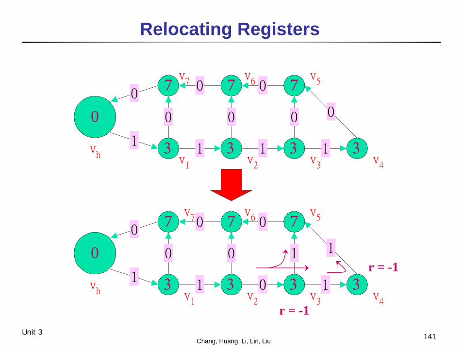
Relocating Registers
7 7 7
3 3 3 3
00
0 0
00 0 0
1 1 11
vh v
1v
2v
3v
4
v5
v6
v7
7 7 7
3 3 3 3
00
0 0
10 0 1
1 0 11
vh v
1v
2v
3v
4
v5
v6
v7
r = -1
r = -1

142Chang, Huang, Li, Lin, LiuUnit 3
Optimal Retiming (1/3)․Problem: Given a graph G, find a legal retiming r of G
such that the clock period Φ(Gr) of the retimed circuit Gris as small as possible.
․Lemma: Let G be a synchronous circuit, and let c be any positive real number, the following are equivlent:1. Φ(G) ≤ c2. For all vertices u and v, if D(u,v) > c, then W(u,v)≥1
․Lemma:⎯ A path p is a critical path of Gr ⇔ it is a critical path of G⎯ Wr (u,v)=W(u,v)+r(v)-r(u)⎯ Dr (u,v)=D(u,v)
․Corollary: Φ(Gr )=D(u,v) for some u,v
143Chang, Huang, Li, Lin, LiuUnit 3
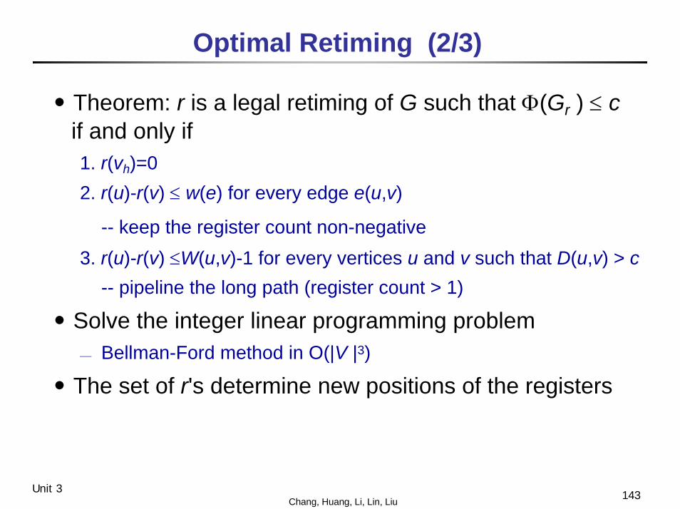
Optimal Retiming (2/3)
․Theorem: r is a legal retiming of G such that Φ(Gr ) ≤ cif and only if1. r(vh)=02. r(u)-r(v) ≤ w(e) for every edge e(u,v)
-- keep the register count non-negative3. r(u)-r(v) ≤W(u,v)-1 for every vertices u and v such that D(u,v) > c
-- pipeline the long path (register count > 1)
․Solve the integer linear programming problem⎯ Bellman-Ford method in O(|V |3)
․The set of r's determine new positions of the registers
144Chang, Huang, Li, Lin, LiuUnit 3
Optimal Retiming (3/3)
․Algorithm of optimal retiming:1. Compute W and D2. Sort the elements in the range of D3. Binary search the minimum achievable clock period by applying
Bellman-Ford algorithm to check the satisfication of the Theorem4. Derive the r(v) from the minimum achievable clock period found
in Step 3
․Complexity O(|V |3 lg|V |)
145Chang, Huang, Li, Lin, LiuUnit 3
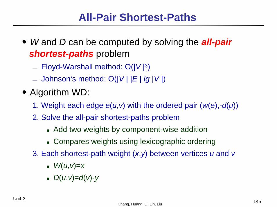
All-Pair Shortest-Paths
․W and D can be computed by solving the all-pair shortest-paths problem⎯ Floyd-Warshall method: O(|V |3)⎯ Johnson‘s method: O(|V | |E | lg |V |)
․Algorithm WD:1. Weight each edge e(u,v) with the ordered pair (w(e),-d(u))2. Solve the all-pair shortest-paths problem
Add two weights by component-wise additionCompares weights using lexicographic ordering
3. Each shortest-path weight (x,y) between vertices u and vW(u,v)=xD(u,v)=d(v)-y

146Chang, Huang, Li, Lin, LiuUnit 3
Examples: W and D Matrixes
7 7 7
3 3 3 3
00 0 0
00 0 0
1 1 11vh v1 v2 v3 v4
v5v6v7
W v1
v1
v2
v2
v3
v3 v4
v4
v5
v5 v6
v6
v7
v7
0000000
01
11
vh
vh
11110
00
00
00
11
2
22222
23
3333
23
1
4
444
0
23
1
0
33 2
0
00
0
00
0
000
21
1D v1
v1
v2
v2
v3
v3 v4
v4
v5
v5 v6
v6
v7
v7
0101724242114
33
2027
vh
vh
272417107
33
37
77
66
6
3030272013
99
33302316
912
6
12
332619
10
1616
13
10
3023 20
14
1717
14
2421
24
101710
1313
10
(source)
(destination)
147Chang, Huang, Li, Lin, LiuUnit 3
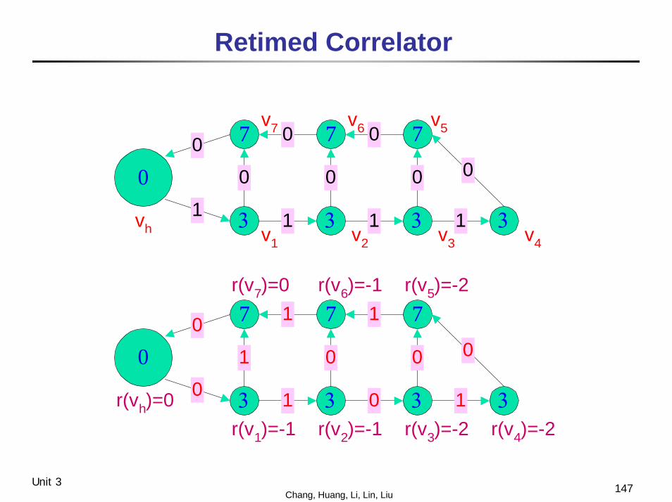
Retimed Correlator
7 7 7
3 3 3 3
00 0 0
00 0 0
1 1 11vh v1 v2 v3 v4
v5v6v7
7 7 7
3 3 3 3
00 1 1
01 0 0
1 0 10
r(v7)=0 r(v6)=-1 r(v5)=-2
r(v4)=-2r(v3)=-2r(v2)=-1r(v1)=-1r(vh)=0
148Chang, Huang, Li, Lin, LiuUnit 3
Retiming and Resynthesis
․Migrate all registers to the periphery of a sub-network⎯ Peripheral retiming
․Optimize the sub-network with any combinational technique⎯ Resynthesis
․Replace registers back in the sub-network⎯ Retiming
․This procedure may further improve the timing across the registers
149Chang, Huang, Li, Lin, LiuUnit 3
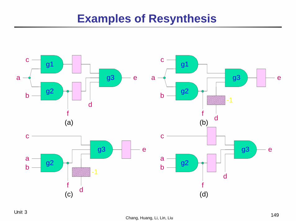
Examples of Resynthesis
g1
g3
df
g2
a
b
c
e
(a)
g1
g3
df
g2
a
b
c
e
(b)
-1
g3
df
g2ab
c
e
(c)
-1
g3
df
g2ab
c
e
(d)

150Chang, Huang, Li, Lin, LiuUnit 3
Peripheral Retiming
․A peripheral retiming is a retiming such that⎯ r(v)=0 where v is an I/O pin⎯ w(u,v)+r(v)-r(u)=0 where e(u,v) in an internal edge
․Move all registers to the peripheral edges․Leave a purely combinational logic block between two
set of registers․Example:
1
o1
i1 i2
c
a b
1
1 2
0
o1
i1 i2
c
a b
2
0 0
1
1

151Chang, Huang, Li, Lin, LiuUnit 3
Conditions for Peripheral Retiming
․No two paths between any input i and any output j have different edge weights
․Exist αi and βj , 1≤ i ≤ m, 1≤ j ≤ n such that Wi,j= αi + βj(m: no. of inputs; n: no. of outputs)
․Wi,j = ∑path ii -> oj w(e) if all paths between input i and output j have the same weight
․Complexity O(e ⋅ min(m,n))
152Chang, Huang, Li, Lin, LiuUnit 3
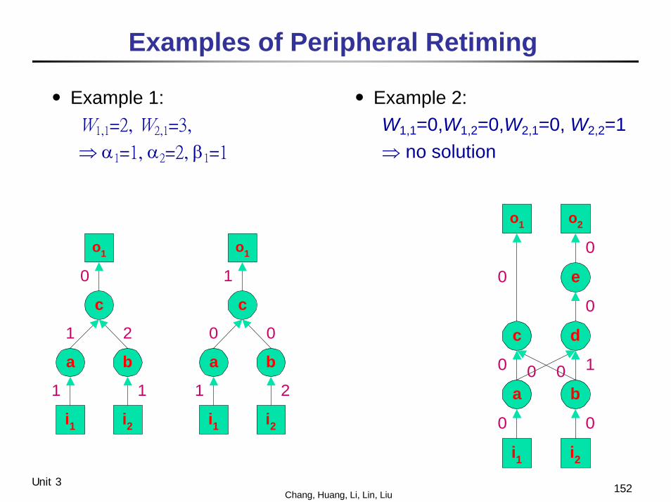
Examples of Peripheral Retiming
․Example 1:W1,1=2, W2,1=3,
⇒ α1=1, α2=2, β1=1
․Example 2:W1,1=0,W1,2=0,W2,1=0, W2,2=1 ⇒ no solution
o1
i1 i2
d
a b
0
0 10
0
o2
c
0
e
0
0
0
1
o1
i1 i2
c
a b
1
1 2
0
o1
i1 i2
c
a b
2
0 0
1
1
153Chang, Huang, Li, Lin, LiuUnit 3
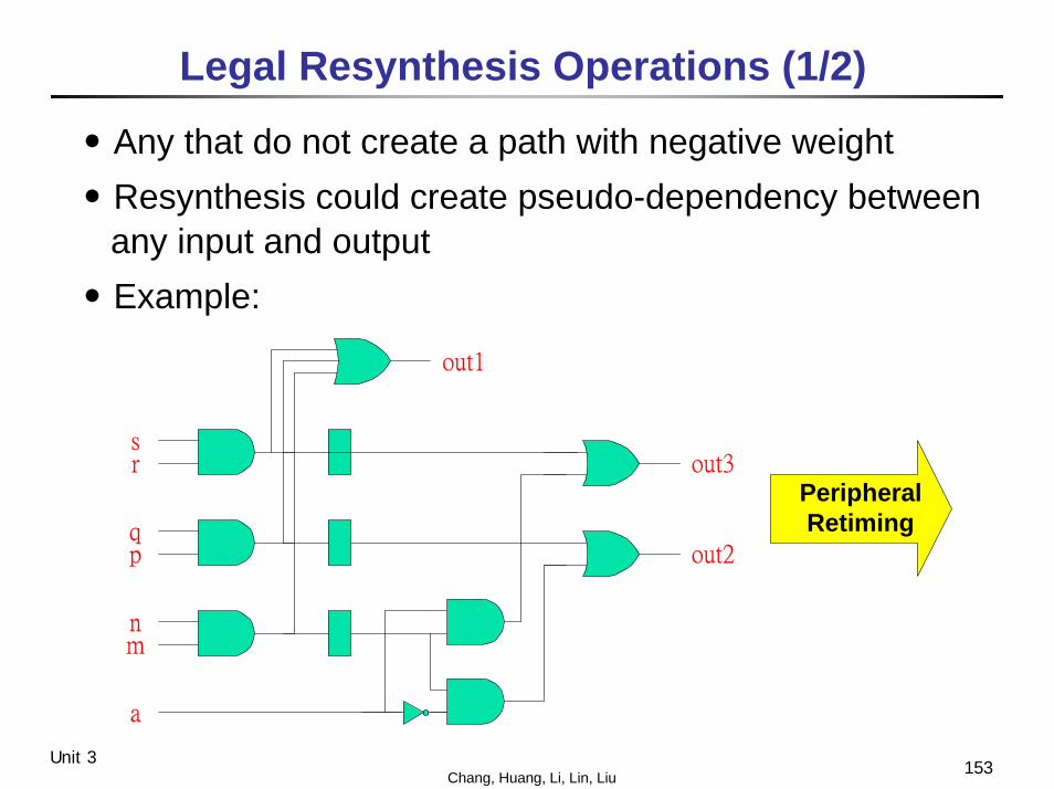
Legal Resynthesis Operations (1/2)
․Any that do not create a path with negative weight․Resynthesis could create pseudo-dependency between
any input and output․Example:
out1
out3
out2
a
mn
pq
rs
PeripheralRetiming
154Chang, Huang, Li, Lin, LiuUnit 3
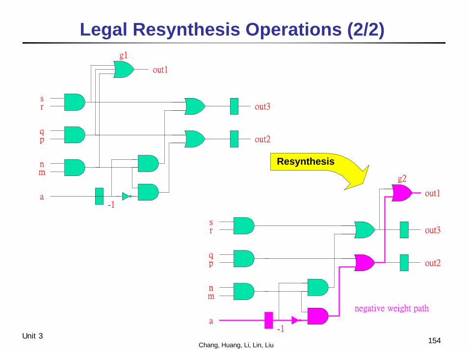
Legal Resynthesis Operations (2/2)g1
out1
out3
out2
a
mn
pq
rs
-1
out1
out3
out2
a
mn
pq
rs
-1
g2
negative weight path
Resynthesis

155Chang, Huang, Li, Lin, LiuUnit 3
Effects of Retiming and Resynthesis
․Area optimization:⎯ No significant improvement⎯ Limitation on existing combinational optimization techniques⎯ Some circuits (pipelined datapaths) have inherently no potential
for further optimization using retiming and resynthesis techniques
․Performance optimization of pipelined circuits:⎯ Significant improvements for pipelined arithmetic circuits
Related Documents


