198 Uniform Sb 2 S 3 optical coatings by chemical spray method Jako S. Eensalu * , Atanas Katerski, Erki Kärber, Ilona Oja Acik, Arvo Mere and Malle Krunks * Full Research Paper Open Access Address: Laboratory of Thin Film Chemical Technologies, Department of Materials and Environmental Technology, Tallinn University of Technology, Ehitajate tee 5, Tallinn 19086, Estonia Email: Jako S. Eensalu * - [email protected]; Malle Krunks * - [email protected] * Corresponding author Keywords: antimony sulfide; thin films; ultrasonic spray; vacuum annealing; Volmer–Weber growth Beilstein J. Nanotechnol. 2019, 10, 198–210. doi:10.3762/bjnano.10.18 Received: 22 September 2018 Accepted: 04 December 2018 Published: 15 January 2019 This article is part of the thematic issue "Chemical thin coating methods for functional nanomaterials". Guest Editor: J. Bachmann © 2019 Eensalu et al.; licensee Beilstein-Institut. License and terms: see end of document. Abstract Antimony sulfide (Sb 2 S 3 ), an environmentally benign material, has been prepared by various deposition methods for use as a solar absorber due to its direct band gap of ≈1.7 eV and high absorption coefficient in the visible light spectrum (1.8 × 10 5 cm −1 at 450 nm). Rapid, scalable, economically viable and controllable in-air growth of continuous, uniform, polycrystalline Sb 2 S 3 absorber layers has not yet been accomplished. This could be achieved with chemical spray pyrolysis, a robust chemical method for deposition of thin films. We applied a two-stage process to produce continuous Sb 2 S 3 optical coatings with uniform thickness. First, amorphous Sb 2 S 3 layers, likely forming by 3D Volmer–Weber island growth through a molten phase reaction between SbCl 3 and SC(NH 2 ) 2 , were deposited in air on a glass/ITO/TiO 2 substrate by ultrasonic spraying of methanolic Sb/S 1:3 molar ratio solu- tion at 200–210 °C. Second, we produced polycrystalline uniform films of Sb 2 S 3 (E g 1.8 eV) with a post-deposition thermal treat- ment of amorphous Sb 2 S 3 layers in vacuum at 170 °C, <4 × 10 −6 Torr for 5 minutes. The effects of the deposition temperature, the precursor molar ratio and the thermal treatment temperature on the Sb 2 S 3 layers were investigated using Raman spectroscopy, X-ray diffraction, scanning electron microscopy, energy dispersive X-ray spectroscopy and UV–vis–NIR spectroscopy. We demon- strated that Sb 2 S 3 optical coatings with controllable structure, morphology and optical properties can be deposited by ultrasonic spray pyrolysis in air by tuning of the deposition temperature, the Sb/S precursor molar ratio in the spray solution, and the post- deposition treatment temperature. 198 Introduction Antimony sulfide (Sb 2 S 3 ) is an environmentally benign materi- al. As Sb and S are abundant elements in the Earth’s crust, enough raw materials can be supplied to manufacture large quantities of Sb 2 S 3 in the long term. Sb 2 S 3 can be applied as the inorganic absorber in solar cells due to its direct band gap of ≈1.7 eV [1,2].

Welcome message from author
This document is posted to help you gain knowledge. Please leave a comment to let me know what you think about it! Share it to your friends and learn new things together.
Transcript
198
Uniform Sb2S3 optical coatings by chemical spray methodJako S. Eensalu*, Atanas Katerski, Erki Kärber, Ilona Oja Acik, Arvo Mereand Malle Krunks*
Full Research Paper Open Access
Address:Laboratory of Thin Film Chemical Technologies, Department ofMaterials and Environmental Technology, Tallinn University ofTechnology, Ehitajate tee 5, Tallinn 19086, Estonia
Email:Jako S. Eensalu* - [email protected]; Malle Krunks* [email protected]
* Corresponding author
Keywords:antimony sulfide; thin films; ultrasonic spray; vacuum annealing;Volmer–Weber growth
Beilstein J. Nanotechnol. 2019, 10, 198–210.doi:10.3762/bjnano.10.18
Received: 22 September 2018Accepted: 04 December 2018Published: 15 January 2019
This article is part of the thematic issue "Chemical thin coating methodsfor functional nanomaterials".
Guest Editor: J. Bachmann
© 2019 Eensalu et al.; licensee Beilstein-Institut.License and terms: see end of document.
AbstractAntimony sulfide (Sb2S3), an environmentally benign material, has been prepared by various deposition methods for use as a solar
absorber due to its direct band gap of ≈1.7 eV and high absorption coefficient in the visible light spectrum (1.8 × 105 cm−1 at
450 nm). Rapid, scalable, economically viable and controllable in-air growth of continuous, uniform, polycrystalline Sb2S3
absorber layers has not yet been accomplished. This could be achieved with chemical spray pyrolysis, a robust chemical method for
deposition of thin films. We applied a two-stage process to produce continuous Sb2S3 optical coatings with uniform thickness.
First, amorphous Sb2S3 layers, likely forming by 3D Volmer–Weber island growth through a molten phase reaction between SbCl3
and SC(NH2)2, were deposited in air on a glass/ITO/TiO2 substrate by ultrasonic spraying of methanolic Sb/S 1:3 molar ratio solu-
tion at 200–210 °C. Second, we produced polycrystalline uniform films of Sb2S3 (Eg 1.8 eV) with a post-deposition thermal treat-
ment of amorphous Sb2S3 layers in vacuum at 170 °C, <4 × 10⁻⁶ Torr for 5 minutes. The effects of the deposition temperature, the
precursor molar ratio and the thermal treatment temperature on the Sb2S3 layers were investigated using Raman spectroscopy,
X-ray diffraction, scanning electron microscopy, energy dispersive X-ray spectroscopy and UV–vis–NIR spectroscopy. We demon-
strated that Sb2S3 optical coatings with controllable structure, morphology and optical properties can be deposited by ultrasonic
spray pyrolysis in air by tuning of the deposition temperature, the Sb/S precursor molar ratio in the spray solution, and the post-
deposition treatment temperature.
198
IntroductionAntimony sulfide (Sb2S3) is an environmentally benign materi-
al. As Sb and S are abundant elements in the Earth’s crust,
enough raw materials can be supplied to manufacture large
quantities of Sb2S3 in the long term. Sb2S3 can be applied as the
inorganic absorber in solar cells due to its direct band gap of
≈1.7 eV [1,2].
Beilstein J. Nanotechnol. 2019, 10, 198–210.
199
Sb2S3, prepared by a chemical bath deposition (CBD) [3,4],
spin coating [5], atomic layer deposition (ALD) [6] or chemical
spray pyrolysis (CSP) [7] method, has been applied in extreme-
ly thin absorber (ETA) solar cells due to its excellent absorp-
tion coefficient in the visible light spectrum (1.8 × 105 cm−1 at
450 nm) [1,2]. Improvements in photocurrent density have been
sought by utilizing a transparent, nanostructured window layer
instead of planar window layers with the ETA Sb2S3 absorber
layer [4,7]. Previous studies show that achieving sufficient
repeatability alongside optimization of the component layers,
i.e., transparent (structured) window layer, Sb2S3 absorber
layer, and hole transport material layer, and their respective
interfaces, is a tremendous undertaking [4].
Attention has surged toward planar heterojunction Sb2S3 solar
cells due to their simpler structure, less intricate production, and
enhanced repeatability vs structured solar cells [8]. Planar
≈1.7 eV absorber layers can be applied in semitransparent solar
cells as well as in tandem solar cells.
Chemical spray pyrolysis (CSP) is a robust and industrially
scalable chemical method for rapid deposition of thin films [9].
Our research group first investigated spray-deposited Sb2S3 by
pneumatically spraying aqueous solutions (tartaric acid added
as complexing agent to prevent hydrolysis [10], akin to studies
by Rajpure et al. [11]) or methanolic solutions of SbCl3.
Following, we studied the effect of the Sb/S precursor molar
ratio in solution on ultrasonically sprayed Sb2S3 layers and
presented the first planar TiO2/Sb2S3/P3HT solar cells com-
prising ultrasonically sprayed Sb2S3 (power conversion effi-
ciency η ≤ 1.9%) [12].
SbCl3 and thiourea (SC(NH2)2) are often used in the field to
deposit Sb2S3 thin films. Spraying the SbCl3/SC(NH2)2 (hence-
forth Sb/S) 1:6 molar ratio solution at 250 °C in air yielded
separate Sb2S3 grains, which did not cover the TiO2 substrate
entirely, whereas spraying the Sb/S 1:3 solution yielded an
inhomogeneous mix of amorphous and polycrystalline Sb2S3
[12]. We learned to produce continuous uniform layers of poly-
crystalline Sb2S3 by a two-step process on ZnO nanorod/TiO2
substrates [7]. In this study, we applied this two-step process,
i.e., depositing amorphous Sb2S3 layers on planar substrates,
followed by post-deposition crystallization.
The aim of this study was to produce crystalline, continuous,
Sb2S3 optical coatings with uniform thickness to be applied as a
photovoltaic absorber by ultrasonic spraying on planar glass/
ITO/TiO2 substrates, followed by a post-deposition treatment.
To this end, we studied the effect of the deposition temperature
(TD), the molar ratio of precursors SbCl3 and thiourea
(SC(NH2)2) in the spray solution, and the post-deposition treat-
ment temperature on the structure, morphology and optical
properties of ultrasonically sprayed Sb2S3 thin films.
Results and DiscussionTwo sequential operations were used to obtain homogeneous
Sb2S3 optical coatings with uniform thickness on planar TiO2
substrates. First, we tuned the deposition temperature and molar
ratio of Sb/S precursors in spray solution to deposit continuous
amorphous Sb2S3 layers. An intimate contact, which is a
prerequisite for high power conversion efficiency in solar
cells [13], is formed at the interface between TiO2 and Sb2S3
during deposition of amorphous Sb2S3 layers. Second, all layers
were thermally treated in an inert environment (vacuum,
<4 × 10⁻⁶ Torr) to induce crystallization, without oxidation.
Preliminary experiments at deposition temperatures lower than
182 °C (decomposition of SC(NH2)2 [14,15]) yielded inhomo-
geneous red-brown layers. Furthermore, in our previous paper,
250 °C was found to be too high a deposition temperature to
obtain sufficient coverage of TiO2 substrate by polycrystalline
Sb2S3 thin films, despite the suitable band gap of 1.6 eV and
high phase purity [12]. Restricted to deposition temperatures in
the range 182–250 °C, we sprayed Sb/S 1:3 and 1:6 molar ratio
precursor solutions at TD = 200, 210, and 220 °C. We varied the
aforementioned parameters to attain the conditions to deposit
dense and homogeneous layers of amorphous Sb2S3, which we
then crystallized by a post-deposition thermal treatment.
Based on the scanning electron microscopy (SEM) images, pre-
liminary experiments revealed that spraying Sb/S 1:6 solutions
consistently yielded twice thinner layers compared to layers
deposited from Sb/S 1:3 solutions. Sb2S3 layers of comparable
thickness were deposited by spraying Sb/S 1:6 solutions for
40 minutes and Sb/S 1:3 solutions for 20 minutes.
The samples are named in the text as follows: A-B-C, where A
is the S/Sb molar ratio in solution, B is the deposition tempera-
ture, and C is the specification of the treatment. [Sb/S molar
ratio in solution: “3” for Sb/S 1:3 or “6” for Sb/S 1:6]-[deposi-
tion temperature: “200”, “210” or “220” (°C)]-[treatment: “As-
dep.” for as-deposited and “170”, “200” or “250” (°C) for sam-
ples thermally treated in vacuum].
The samples in which Sb2S3 layers were deposited from either
Sb/S 1:3 or 1:6 solution at TD = 200 °C, followed by thermal
treatment in vacuum at 200 °C (3-200-200, 6-200-200),
contain no Sb2S3, as it likely volatilized completely during the
vacuum thermal treatment. Likewise, treating the Sb2S3 layers
at temperatures higher than 200 °C caused Sb2S3 to completely
volatilize during treatment. Photographs of the samples (Figure
S1) and the description of the vapor pressure calculations
Beilstein J. Nanotechnol. 2019, 10, 198–210.
200
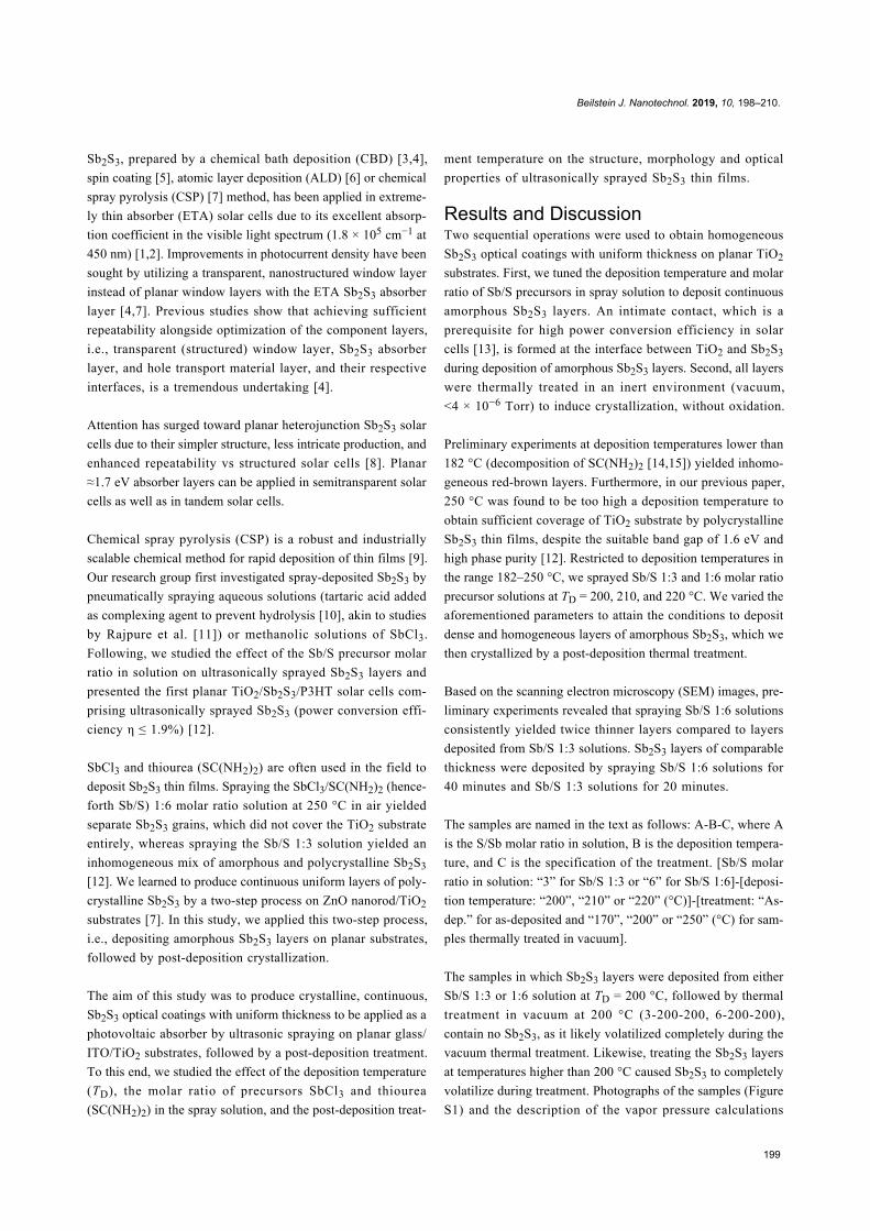
Figure 1: Raman spectra (shifted for visibility) of the as-deposited and thermally treated Sb2S3 films deposited from Sb/S 1:3 (A) or 1:6 (B) solution at200, 210, 220 °C. Examples of deconvoluted fitted band curves are presented for the lowermost spectra. Sample names in figures: [S/Sb molar ratioin solution]-[deposition temperature]-[thermal treatment temperature].
Table 1: Raman band centers and assigned active modes for the studied Sb2S3 layers.
Center of Raman band, cm−1 Symmetry Vibrational mode, [21-23]This study Ref. [21] Ref. [20] Ref. [21] Ref. [20]
126 125 129 Ag Ag lattice mode155 156 158 Ag Ag/B2g lattice mode188 189 186 B1g B1g antisym. S–Sb–S bending237 237 239 B1g B1g/B3g symmetric S–Sb–S bending281 281 282 Ag Ag/B2g antisym. S–Sb–S stretching301 300 299 Ag Ag/B2g antisym. S–Sb–S stretching310 310 312 Ag Ag/B2g symmetric S–Sb–S stretching
(Comment S1) are provided in the Supporting Information
File 1. Consequently, only as-deposited samples and samples
thermally treated in vacuum at 170 °C and 200 °C are eligible
for discussion.
Structure of as-deposited and thermallytreated Sb2S3 layersRaman spectroscopy provides quantitative and qualitative infor-
mation on the vibrational modes in solids. The wide Raman
band centered at 290 cm−1 [12,16] associated with metastibnite,
i.e., amorphous Sb2S3, is characteristic of as-deposited orange
colored (photograph in Supporting Information File 1, Figure
S1) samples (3-200-As-dep., 3-210-As-dep., Figure 1A; 6-200-
As-dep., Figure 1B). The band centered at 145 cm−1 is a low
frequency Eg vibrational mode of anatase-TiO2 [17], which is
observed due to the laser beam penetrating to the substrate
[12,16] through the discontinuous Sb2S3 layers. The TiO2
vibrational band is absent in spectra of Sb2S3 layers containing
less pinholes, as the signal is captured only from Sb2S3.
The narrower bands, attributed to orthorhombic Sb2S3 [16,18-
20], are present in the spectra of as-deposited and thermally
treated lustrous gray (photograph in Supporting Information
File 1, Figure S1) samples (3-200-170, 3-210-170, 3-210-200,
3-220-As-dep., 3-220-170, 3-220-200, Figure 1A; 6-200-170,
6-210-As-dep., 6-210-170, 6-210-200, 6-220-As-dep., 6-220-
170, 6-220-200, Figure 1B; photograph in Supporting Informa-
tion File 1, Figure S1). According to group theory,
orthorhombic Sb2S3 has 30 predicted Raman active modes:
ΓRaman = 10Ag + 5B1g + 10B2g + 5B3g [18,20]. The Raman
spectra were deconvoluted using Lorentzian fitting into vibra-
tional bands of Sb2S3 based on the literature [12,16,21,22]. The
centers of the bands of Sb2S3 in the deconvoluted Raman spec-
tra (Table 1, symmetries taken from [20,21]) are similar to
Beilstein J. Nanotechnol. 2019, 10, 198–210.
201
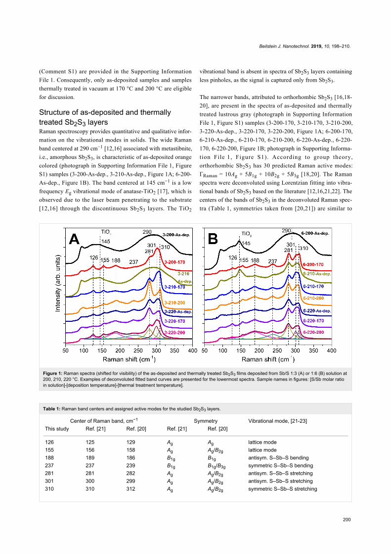
Figure 2: XRD patterns (shifted for visibility) of as-deposited and vacuum treated (170 °C or 200 °C, 5 minutes) Sb2S3 layers deposited on glass/ITO/TiO2 substrate from Sb/S 1:3 (A) or 1:6 (B) solution at Ts = 200, 210, 220 °C. Sample names in figures: [S/Sb molar ratio in solution]-[deposition tem-perature]-[thermal treatment temperature].
values reported in our previous studies [7,12]. Band centers,
relative single peak intensities and full widths at half maximum
(FWHM) of the narrow bands centered at 281, 301 and
310 cm−1 can be respectively found in Tables S1, S2, and S3 of
Supporting Information File 1.
The FWHM of the vibrational band centered at 281 cm−1
narrows from ≈24 cm−1 to 21–23 cm−1 after vacuum thermal
treatment of the samples deposited at 210–220 °C from both
Sb/S 1:3 and Sb/S 1:6 solutions (3-210-170, 3-220-170, 6-210-
170 and 6-220-170) at 170 °C (3-210-170, 3-220-170, 6-210-
170 and 6-220-170) and narrows by 5 cm−1 at most after
vacuum thermal treatment at 200 °C (3-210-200). The
narrowing of the Raman bands due to thermal treatment leads
us to suppose that crystallization continues during the vacuum
thermal treatment and proceeds further at higher thermal treat-
ment temperatures [16]. The vibrational bands corresponding to
Sb2O3 were not detected by Raman spectroscopy in any of the
studied glass/ITO/TiO2/Sb2S3 samples.
X-ray diffraction (XRD) provides qualitative information on the
phase composition and crystal structure. XRD patterns of refer-
ence glass/ITO/TiO2 samples and samples containing XRD-
amorphous Sb2S3 (3-200-As-dep., 3-210-As-dep., Figure 2A;
6-200-As-dep., Figure 2B) show only diffraction peaks corre-
sponding to cubic In2O3 (2θ = 21.3°, 30.4°, 35.3°, 37.4°, 41.4°,
45.3°, ICDD PDF 03-065-3170) and anatase-TiO2 (25.3°,
48.2°, ICDD PDF 00-016-0617). The diffraction peaks of
orthorhombic Sb2S3 (ICDD PDF 01-075-4012), space group
Pnma (D2h16) [20,24,25], appear in XRD patterns of lustrous
gray as-deposited and thermally treated Sb2S3 samples (3-200-
170, 3-210-170, 3-210-200, 3-220-As-dep., 3-220-170, 3-220-
200, Figure 2A; 6-200-170, 6-210-As-dep., 6-210-170, 6-210-
200, 6-220-As-dep., 6-220-170, 6-220-200, Figure 2B). The 2θ
angles of observed Sb2S3 diffraction peaks and corresponding
crystal plane indices are presented in Supporting Information
File 1, Table S4. Experimentally determined mean lattice con-
stants a, b and c of Sb2S3 are 11.25 ± 0.07 Å, 3.810 ± 0.025 Å
and 11.16 ± 0.07 Å, respectively. Our experimentally deter-
Beilstein J. Nanotechnol. 2019, 10, 198–210.
202
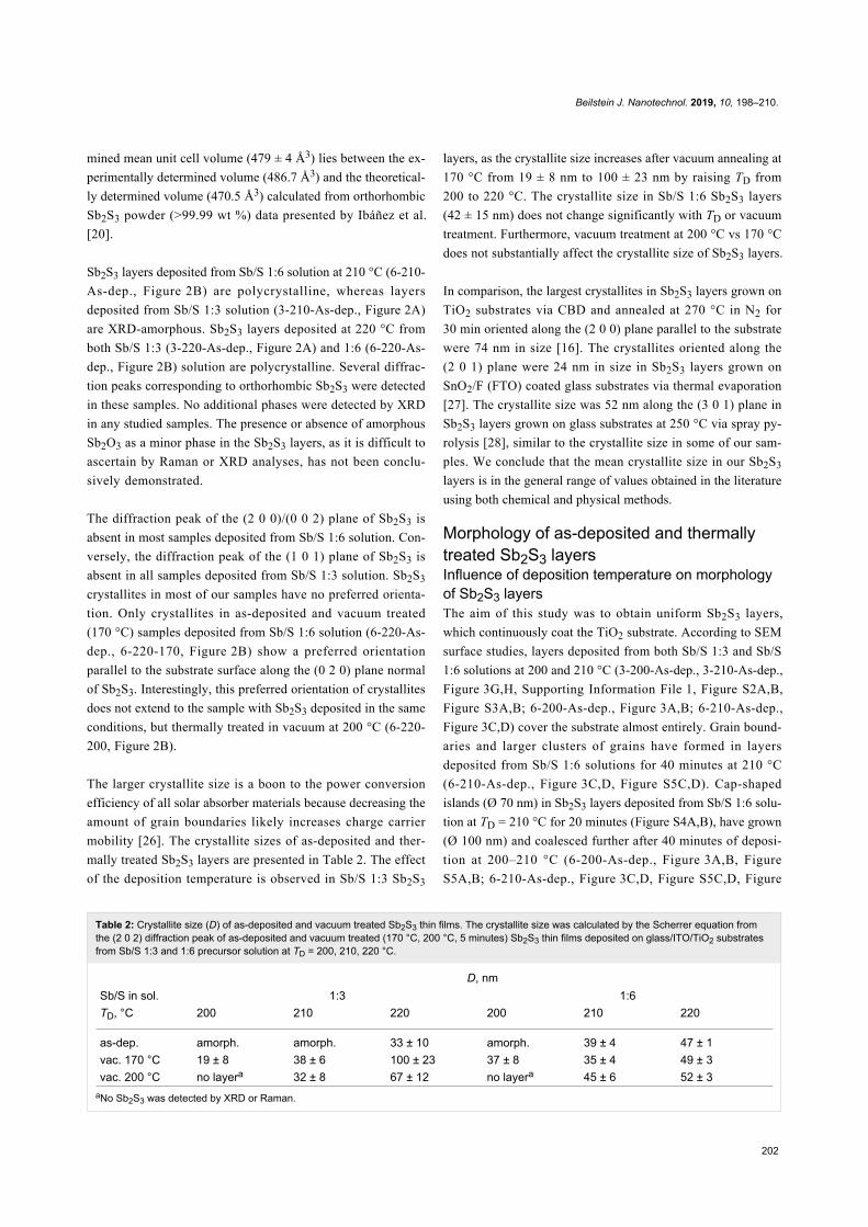
Table 2: Crystallite size (D) of as-deposited and vacuum treated Sb2S3 thin films. The crystallite size was calculated by the Scherrer equation fromthe (2 0 2) diffraction peak of as-deposited and vacuum treated (170 °C, 200 °C, 5 minutes) Sb2S3 thin films deposited on glass/ITO/TiO2 substratesfrom Sb/S 1:3 and 1:6 precursor solution at TD = 200, 210, 220 °C.
D, nmSb/S in sol. 1:3 1:6TD, °C 200 210 220 200 210 220
as-dep. amorph. amorph. 33 ± 10 amorph. 39 ± 4 47 ± 1vac. 170 °C 19 ± 8 38 ± 6 100 ± 23 37 ± 8 35 ± 4 49 ± 3vac. 200 °C no layera 32 ± 8 67 ± 12 no layera 45 ± 6 52 ± 3
aNo Sb2S3 was detected by XRD or Raman.
mined mean unit cell volume (479 ± 4 Å3) lies between the ex-
perimentally determined volume (486.7 Å3) and the theoretical-
ly determined volume (470.5 Å3) calculated from orthorhombic
Sb2S3 powder (>99.99 wt %) data presented by Ibáñez et al.
[20].
Sb2S3 layers deposited from Sb/S 1:6 solution at 210 °C (6-210-
As-dep., Figure 2B) are polycrystalline, whereas layers
deposited from Sb/S 1:3 solution (3-210-As-dep., Figure 2A)
are XRD-amorphous. Sb2S3 layers deposited at 220 °C from
both Sb/S 1:3 (3-220-As-dep., Figure 2A) and 1:6 (6-220-As-
dep., Figure 2B) solution are polycrystalline. Several diffrac-
tion peaks corresponding to orthorhombic Sb2S3 were detected
in these samples. No additional phases were detected by XRD
in any studied samples. The presence or absence of amorphous
Sb2O3 as a minor phase in the Sb2S3 layers, as it is difficult to
ascertain by Raman or XRD analyses, has not been conclu-
sively demonstrated.
The diffraction peak of the (2 0 0)/(0 0 2) plane of Sb2S3 is
absent in most samples deposited from Sb/S 1:6 solution. Con-
versely, the diffraction peak of the (1 0 1) plane of Sb2S3 is
absent in all samples deposited from Sb/S 1:3 solution. Sb2S3
crystallites in most of our samples have no preferred orienta-
tion. Only crystallites in as-deposited and vacuum treated
(170 °C) samples deposited from Sb/S 1:6 solution (6-220-As-
dep., 6-220-170, Figure 2B) show a preferred orientation
parallel to the substrate surface along the (0 2 0) plane normal
of Sb2S3. Interestingly, this preferred orientation of crystallites
does not extend to the sample with Sb2S3 deposited in the same
conditions, but thermally treated in vacuum at 200 °C (6-220-
200, Figure 2B).
The larger crystallite size is a boon to the power conversion
efficiency of all solar absorber materials because decreasing the
amount of grain boundaries likely increases charge carrier
mobility [26]. The crystallite sizes of as-deposited and ther-
mally treated Sb2S3 layers are presented in Table 2. The effect
of the deposition temperature is observed in Sb/S 1:3 Sb2S3
layers, as the crystallite size increases after vacuum annealing at
170 °C from 19 ± 8 nm to 100 ± 23 nm by raising TD from
200 to 220 °C. The crystallite size in Sb/S 1:6 Sb2S3 layers
(42 ± 15 nm) does not change significantly with TD or vacuum
treatment. Furthermore, vacuum treatment at 200 °C vs 170 °C
does not substantially affect the crystallite size of Sb2S3 layers.
In comparison, the largest crystallites in Sb2S3 layers grown on
TiO2 substrates via CBD and annealed at 270 °C in N2 for
30 min oriented along the (2 0 0) plane parallel to the substrate
were 74 nm in size [16]. The crystallites oriented along the
(2 0 1) plane were 24 nm in size in Sb2S3 layers grown on
SnO2/F (FTO) coated glass substrates via thermal evaporation
[27]. The crystallite size was 52 nm along the (3 0 1) plane in
Sb2S3 layers grown on glass substrates at 250 °C via spray py-
rolysis [28], similar to the crystallite size in some of our sam-
ples. We conclude that the mean crystallite size in our Sb2S3
layers is in the general range of values obtained in the literature
using both chemical and physical methods.
Morphology of as-deposited and thermallytreated Sb2S3 layersInfluence of deposition temperature on morphologyof Sb2S3 layersThe aim of this study was to obtain uniform Sb2S3 layers,
which continuously coat the TiO2 substrate. According to SEM
surface studies, layers deposited from both Sb/S 1:3 and Sb/S
1:6 solutions at 200 and 210 °C (3-200-As-dep., 3-210-As-dep.,
Figure 3G,H, Supporting Information File 1, Figure S2A,B,
Figure S3A,B; 6-200-As-dep., Figure 3A,B; 6-210-As-dep.,
Figure 3C,D) cover the substrate almost entirely. Grain bound-
aries and larger clusters of grains have formed in layers
deposited from Sb/S 1:6 solutions for 40 minutes at 210 °C
(6-210-As-dep., Figure 3C,D, Figure S5C,D). Cap-shaped
islands (Ø 70 nm) in Sb2S3 layers deposited from Sb/S 1:6 solu-
tion at TD = 210 °C for 20 minutes (Figure S4A,B), have grown
(Ø 100 nm) and coalesced further after 40 minutes of deposi-
tion at 200–210 °C (6-200-As-dep., Figure 3A,B, Figure
S5A,B; 6-210-As-dep., Figure 3C,D, Figure S5C,D, Figure
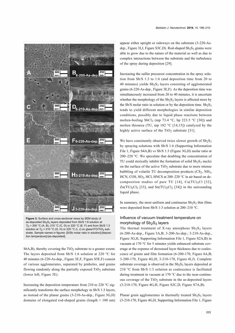
Beilstein J. Nanotechnol. 2019, 10, 198–210.
203
Figure 3: Surface and cross-sectional views by SEM study ofas-deposited Sb2S3 layers deposited from Sb/S 1:6 solution atTD = 200 °C (A, B), 210 °C (C, D) or 220 °C (E, F) and from Sb/S 1:3solution at TD = 210 °C (G, H) or 220 °C (I, J) on glass/ITO/TiO2 sub-strate. Sample names in figures: [S/Sb molar ratio in solution]-[deposi-tion temperature]-[as-deposited].
S6A,B), thereby covering the TiO2 substrate to a greater extent.
The layers deposited from Sb/S 1:6 solution at 220 °C for
40 minutes (6-220-As-dep., Figure 3E,F, Figure S5E,F) consist
of various agglomerates, separated by pinholes, and grains
flowing randomly along the partially exposed TiO2 substrate
(lower left, Figure 3E).
Increasing the deposition temperature from 210 to 220 °C sig-
nificantly transforms the surface morphology in Sb/S 1:3 layers,
as instead of the planar grains (3-210-As-dep., Figure 3G,H)
domains of elongated rod-shaped grains (length ≈ 100 nm)
appear either upright or sideways on the substrate (3-220-As-
dep., Figure 3I,J, Figure S3C,D). Rod-shaped Sb2S3 grains were
able to grow due to the nature of the material as well as due to
complex interactions between the substrate and the turbulence
of the spray during deposition [29].
Increasing the sulfur precursor concentration in the spray solu-
tion from Sb/S 1:3 to 1:6 (and deposition time from 20 to
40 minutes) yields Sb2S3 layers consisting of agglomerated
grains (6-220-As-dep., Figure 3E,F). As the deposition time was
simultaneously increased from 20 to 40 minutes, it is uncertain
whether the morphology of the Sb2S3 layers is affected more by
the Sb/S molar ratio in solution or by the deposition time. Sb2S3
tends to yield different morphologies in similar deposition
conditions, possibly due to liquid phase reactions between
molten-boiling SbCl3 (mp 73.4 °C, bp 223.5 °C [30]) and
molten thiourea (TU, mp 182 °C [14,15]) catalyzed by the
highly active surface of the TiO2 substrate [31].
We have consistently observed twice slower growth of Sb2S3
by spraying solutions with Sb/S 1:6 (Supporting Information
File 1, Figure S4A,B) vs Sb/S 1:3 (Figure 3G,H) molar ratio at
200–220 °C. We speculate that doubling the concentration of
TU could sterically inhibit the formation of solid Sb2S3 nuclei
on the surface of the active TiO2 substrate due to more intense
bubbling of volatile TU decomposition products (CS2, NH3,
HCN, COS, SO2, HCl, HNCS at 200–220 °C in air based on de-
composition studies of pure TU [14], Cu(TU)3Cl [32],
Zn(TU)2Cl2 [33], and Sn(TU)2Cl2 [34]) in the surrounding
liquid phase.
In summary, the most uniform and continuous Sb2S3 thin films
were deposited from Sb/S 1:3 solution at 200–210 °C.
Influence of vacuum treatment temperature onmorphology of Sb2S3 layersThe thermal treatment of X-ray amorphous Sb2S3 layers
(6-200-As-dep., Figure 3A,B; 3-200-As-dep.; 3-210-As-dep.,
Figure 3G,H, Supporting Information File 1, Figure S2A,B) in
vacuum at 170 °C for 5 minutes yields enhanced substrate cov-
erage at the expense of decreased layer thickness due to coales-
cence of grains and film formation (6-200-170, Figure 4A,B;
3-200-170, Figure 4G,H; 3-210-170, Figure 4I,J). Complete
substrate coverage is observed in the Sb2S3 layers deposited at
210 °C from Sb/S 1:3 solution as coalescence is facilitated
during treatment in vacuum at 170 °C due to the near-continu-
ous coverage of the TiO2 substrate in the as-deposited layers
(3-210-170, Figure 4G,H, Figure S2C,D, Figure S7A,B).
Planar grain agglomerates in thermally treated Sb2S3 layers
(3-210-170, Figure 4G,H, Supporting Information File 1, Figure
Beilstein J. Nanotechnol. 2019, 10, 198–210.
204
Table 3: Thicknesses of Sb2S3 layers estimated from SEM images.
Sb2S3 layer thickness, nmSb/S 1:3 in sol., 20 min dep. Sb/S 1:6 in sol., 40 min dep.
TD, °C 200 210 220 200 210 220as-dep. 70–90 80–100 60/150a 50–70 60/400a 40/400a
vac., 170 °C 70–90 70–90 80/150a 30–40 60/400a 40/400a
vac., 200 °C no layerb 60–70 N/A no layerb 60–70 N/AaThickness of formations shown in the Supporting Information File 1 in Figures S5, S7, S8 and S9. bNo Sb2S3 was detected by XRD or Raman.
Figure 4: Surface and cross-sectional views by SEM study of ther-mally treated (170 °C, 5 minutes) Sb2S3 layers deposited from Sb/S1:6 solution at TD = 200 °C (A, B), 210 °C (C, D) or 220 °C (E, F) andfrom Sb/S 1:3 solution at TD = 210 °C (G, H) or 220 °C (I, J) on glass/ITO/TiO2 substrates. Sample names in figures: [S/Sb molar ratio insolution]-[deposition temperature]-[thermal treatment temperature].
S7A,B; 6-200-170, Figure 4A,B, Figure S9A,B; 6-210-170,
Figure 4C,D, Figure S9C,D) range from 100 nm to over 10 µm
in size. These agglomerates, consisting of smaller grains sepa-
rated by ridges, resemble the surface morphology of 300 nm
thick polycrystalline Sb2S3 films grown via thermal evapora-
tion and annealed for 10 min at 300 °C in N2 [35], and that of
metal halide perovskites obtained by Volmer–Weber growth via
hot casting [36]. The layers deposited at 220 °C from both Sb/S
1:3 and Sb/S 1:6 solutions, and thermally treated at 170 °C,
consist of numerous grains and pinholes (3-220-170,
Figure 4I,J; 6-220-170, Figure 4E,F).
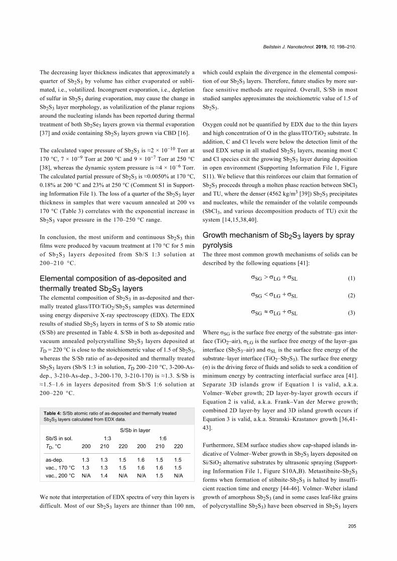
Sb2S3 layers deposited at 210 °C from both Sb/S 1:3 and Sb/S
1:6 solutions, and thermally treated in vacuum at 200 °C
(3-210-200, Figure 5A,B, Supporting Information File 1, Figure
S8A,C,E; 6-210-200, Figure 5C,D, Figure S8B,D,F), are
porous, inhomogeneous and ≈20 nm thinner (Table 3) vs the
uniform in thickness layers after treatment at 170 °C (3-210-
170, Figure 4I,J; 6-210-170, Figure 4C,D).
Figure 5: Surface and cross-sectional views by SEM study of vacuumtreated (200 °C, 5 minutes) Sb2S3 layers deposited from Sb/S 1:6solution (A, B) and from Sb/S 1:3 solution (C, D) at TD = 210 °C onglass/ITO/TiO2 substrates. Sample names in figures: [S/Sb molar ratioin solution]-[deposition temperature]-[thermal treatment temperature].
Beilstein J. Nanotechnol. 2019, 10, 198–210.
205
The decreasing layer thickness indicates that approximately a
quarter of Sb2S3 by volume has either evaporated or subli-
mated, i.e., volatilized. Incongruent evaporation, i.e., depletion
of sulfur in Sb2S3 during evaporation, may cause the change in
Sb2S3 layer morphology, as volatilization of the planar regions
around the nucleating islands has been reported during thermal
treatment of both Sb2Se3 layers grown via thermal evaporation
[37] and oxide containing Sb2S3 layers grown via CBD [16].
The calculated vapor pressure of Sb2S3 is ≈2 × 10⁻¹⁰ Torr at
170 °C, 7 × 10⁻⁹ Torr at 200 °C and 9 × 10⁻⁷ Torr at 250 °C
[38], whereas the dynamic system pressure is ≈4 × 10⁻⁶ Torr.
The calculated partial pressure of Sb2S3 is ≈0.0050% at 170 °C,
0.18% at 200 °C and 23% at 250 °C (Comment S1 in Support-
ing Information File 1). The loss of a quarter of the Sb2S3 layer
thickness in samples that were vacuum annealed at 200 vs
170 °C (Table 3) correlates with the exponential increase in
Sb2S3 vapor pressure in the 170–250 °C range.
In conclusion, the most uniform and continuous Sb2S3 thin
films were produced by vacuum treatment at 170 °C for 5 min
of Sb2S3 layers deposited from Sb/S 1:3 solution at
200–210 °C.
Elemental composition of as-deposited andthermally treated Sb2S3 layersThe elemental composition of Sb2S3 in as-deposited and ther-
mally treated glass/ITO/TiO2/Sb2S3 samples was determined
using energy dispersive X-ray spectroscopy (EDX). The EDX
results of studied Sb2S3 layers in terms of S to Sb atomic ratio
(S/Sb) are presented in Table 4. S/Sb in both as-deposited and
vacuum annealed polycrystalline Sb2S3 layers deposited at
TD = 220 °C is close to the stoichiometric value of 1.5 of Sb2S3,
whereas the S/Sb ratio of as-deposited and thermally treated
Sb2S3 layers (Sb/S 1:3 in solution, TD 200–210 °C, 3-200-As-
dep., 3-210-As-dep., 3-200-170, 3-210-170) is ≈1.3. S/Sb is
≈1.5–1.6 in layers deposited from Sb/S 1:6 solution at
200–220 °C.
Table 4: S/Sb atomic ratio of as-deposited and thermally treatedSb2S3 layers calculated from EDX data.
S/Sb in layerSb/S in sol. 1:3 1:6TD, °C 200 210 220 200 210 220
as-dep. 1.3 1.3 1.5 1.6 1.5 1.5vac., 170 °C 1.3 1.3 1.5 1.6 1.6 1.5vac., 200 °C N/A 1.4 N/A N/A 1.5 N/A
We note that interpretation of EDX spectra of very thin layers is
difficult. Most of our Sb2S3 layers are thinner than 100 nm,
which could explain the divergence in the elemental composi-
tion of our Sb2S3 layers. Therefore, future studies by more sur-
face sensitive methods are required. Overall, S/Sb in most
studied samples approximates the stoichiometric value of 1.5 of
Sb2S3.
Oxygen could not be quantified by EDX due to the thin layers
and high concentration of O in the glass/ITO/TiO2 substrate. In
addition, C and Cl levels were below the detection limit of the
used EDX setup in all studied Sb2S3 layers, meaning most C
and Cl species exit the growing Sb2S3 layer during deposition
in open environment (Supporting Information File 1, Figure
S11). We believe that this reinforces our claim that formation of
Sb2S3 proceeds through a molten phase reaction between SbCl3
and TU, where the denser (4562 kg/m3 [39]) Sb2S3 precipitates
and nucleates, while the remainder of the volatile compounds
(SbCl3, and various decomposition products of TU) exit the
system [14,15,38,40].
Growth mechanism of Sb2S3 layers by spraypyrolysisThe three most common growth mechanisms of solids can be
described by the following equations [41]:
(1)
(2)
(3)
Where σSG is the surface free energy of the substrate–gas inter-
face (TiO2–air), σLG is the surface free energy of the layer–gas
interface (Sb2S3–air) and σSL is the surface free energy of the
substrate–layer interface (TiO2–Sb2S3). The surface free energy
(σ) is the driving force of fluids and solids to seek a condition of
minimum energy by contracting interfacial surface area [41].
Separate 3D islands grow if Equation 1 is valid, a.k.a.
Volmer–Weber growth; 2D layer-by-layer growth occurs if
Equation 2 is valid, a.k.a. Frank–Van der Merwe growth;
combined 2D layer-by layer and 3D island growth occurs if
Equation 3 is valid, a.k.a. Stranski–Krastanov growth [36,41-
43].
Furthermore, SEM surface studies show cap-shaped islands in-
dicative of Volmer–Weber growth in Sb2S3 layers deposited on
Si/SiO2 alternative substrates by ultrasonic spraying (Support-
ing Information File 1, Figure S10A,B). Metastibnite-Sb2S3
forms when formation of stibnite-Sb2S3 is halted by insuffi-
cient reaction time and energy [44-46]. Volmer–Weber island
growth of amorphous Sb2S3 (and in some cases leaf-like grains
of polycrystalline Sb2S3) have been observed in Sb2S3 layers
Beilstein J. Nanotechnol. 2019, 10, 198–210.
206
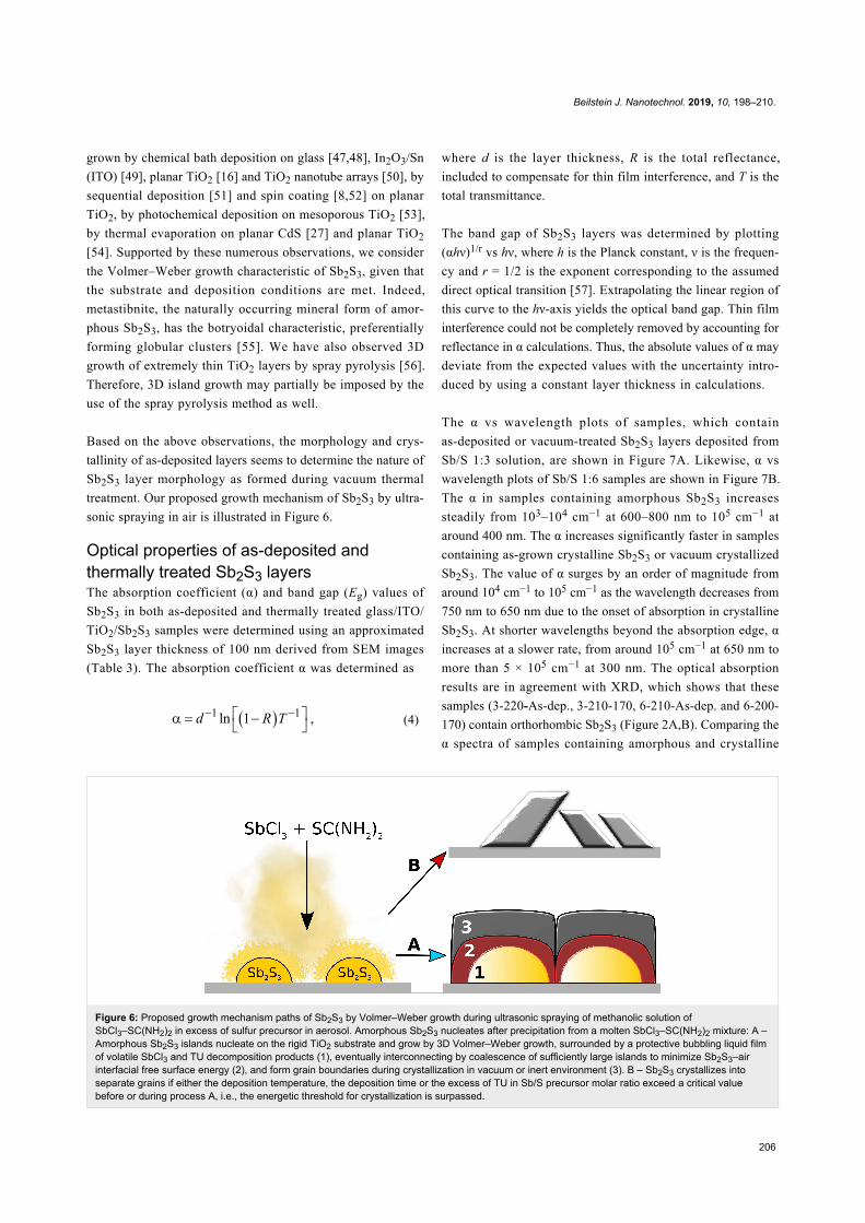
Figure 6: Proposed growth mechanism paths of Sb2S3 by Volmer–Weber growth during ultrasonic spraying of methanolic solution ofSbCl3–SC(NH2)2 in excess of sulfur precursor in aerosol. Amorphous Sb2S3 nucleates after precipitation from a molten SbCl3–SC(NH2)2 mixture: A –Amorphous Sb2S3 islands nucleate on the rigid TiO2 substrate and grow by 3D Volmer–Weber growth, surrounded by a protective bubbling liquid filmof volatile SbCl3 and TU decomposition products (1), eventually interconnecting by coalescence of sufficiently large islands to minimize Sb2S3–airinterfacial free surface energy (2), and form grain boundaries during crystallization in vacuum or inert environment (3). B – Sb2S3 crystallizes intoseparate grains if either the deposition temperature, the deposition time or the excess of TU in Sb/S precursor molar ratio exceed a critical valuebefore or during process A, i.e., the energetic threshold for crystallization is surpassed.
grown by chemical bath deposition on glass [47,48], In2O3/Sn
(ITO) [49], planar TiO2 [16] and TiO2 nanotube arrays [50], by
sequential deposition [51] and spin coating [8,52] on planar
TiO2, by photochemical deposition on mesoporous TiO2 [53],
by thermal evaporation on planar CdS [27] and planar TiO2
[54]. Supported by these numerous observations, we consider
the Volmer–Weber growth characteristic of Sb2S3, given that
the substrate and deposition conditions are met. Indeed,
metastibnite, the naturally occurring mineral form of amor-
phous Sb2S3, has the botryoidal characteristic, preferentially
forming globular clusters [55]. We have also observed 3D
growth of extremely thin TiO2 layers by spray pyrolysis [56].
Therefore, 3D island growth may partially be imposed by the
use of the spray pyrolysis method as well.
Based on the above observations, the morphology and crys-
tallinity of as-deposited layers seems to determine the nature of
Sb2S3 layer morphology as formed during vacuum thermal
treatment. Our proposed growth mechanism of Sb2S3 by ultra-
sonic spraying in air is illustrated in Figure 6.
Optical properties of as-deposited andthermally treated Sb2S3 layersThe absorption coefficient (α) and band gap (Eg) values of
Sb2S3 in both as-deposited and thermally treated glass/ITO/
TiO2/Sb2S3 samples were determined using an approximated
Sb2S3 layer thickness of 100 nm derived from SEM images
(Table 3). The absorption coefficient α was determined as
(4)
where d is the layer thickness, R is the total reflectance,
included to compensate for thin film interference, and T is the
total transmittance.
The band gap of Sb2S3 layers was determined by plotting
(αhν)1/r vs hν, where h is the Planck constant, ν is the frequen-
cy and r = 1/2 is the exponent corresponding to the assumed
direct optical transition [57]. Extrapolating the linear region of
this curve to the hν-axis yields the optical band gap. Thin film
interference could not be completely removed by accounting for
reflectance in α calculations. Thus, the absolute values of α may
deviate from the expected values with the uncertainty intro-
duced by using a constant layer thickness in calculations.
The α vs wavelength plots of samples, which contain
as-deposited or vacuum-treated Sb2S3 layers deposited from
Sb/S 1:3 solution, are shown in Figure 7A. Likewise, α vs
wavelength plots of Sb/S 1:6 samples are shown in Figure 7B.
The α in samples containing amorphous Sb2S3 increases
steadily from 103–104 cm−1 at 600–800 nm to 105 cm−1 at
around 400 nm. The α increases significantly faster in samples
containing as-grown crystalline Sb2S3 or vacuum crystallized
Sb2S3. The value of α surges by an order of magnitude from
around 104 cm−1 to 105 cm−1 as the wavelength decreases from
750 nm to 650 nm due to the onset of absorption in crystalline
Sb2S3. At shorter wavelengths beyond the absorption edge, α
increases at a slower rate, from around 105 cm−1 at 650 nm to
more than 5 × 105 cm−1 at 300 nm. The optical absorption
results are in agreement with XRD, which shows that these
samples (3-220-As-dep., 3-210-170, 6-210-As-dep. and 6-200-
170) contain orthorhombic Sb2S3 (Figure 2A,B). Comparing the
α spectra of samples containing amorphous and crystalline
Beilstein J. Nanotechnol. 2019, 10, 198–210.
207
Figure 7: Absorption coefficient (α) vs wavelength of glass/ITO/TiO2/Sb2S3 samples incorporating as-deposited and vacuum treated (170 °C,5 minutes) Sb2S3 layers. The α of glass/ITO/TiO2 substrates is not shown as it is negligible at the presented wavelengths. Sb2S3 layers weredeposited from Sb/S 1:3 solution at 210 °C, 220 °C (A) and from Sb/S 1:6 solution at 200 °C and 210 °C (B).
Sb2S3 further confirms that the Sb2S3 layers deposited from
Sb/S 1:3 solution at 200–210 °C, and from Sb/S 1:6 solution at
200 °C, are indeed amorphous. Namely, α is an order of magni-
tude smaller at around 600 nm in samples containing amor-
phous Sb2S3 layers (3-210-As-dep. and 6-200-As-dep.).
The experimentally determined Eg are ≈2.7 and 1.8 eV for
amorphous and polycrystalline Sb2S3, respectively (Table 5,
Tauc plots in Supporting Information File 1, Figure S12). In
comparison, Eg of amorphous CBD-Sb2S3 on glass substrates is
≈2.5 eV [58] and Eg of polycrystalline Sb2S3 prepared by physi-
cal and chemical methods is commonly reported as 1.6–1.8 eV
[1,22,58-60]. As such, we find the Eg of our polycrystalline
Sb2S3 layers lies satisfactorily in the range of published values.
Table 5: Band gap (Eg) of as-deposited and thermally treated Sb2S3layers, as estimated assuming direct optical transition and Tauc plotsa
of optical transmittance spectra of glass/ITO/TiO2/Sb2S3 samples.
Eg, eVSb/S in sol. 1:3 1:6TD, °C 200 210 220 200 210 220
as-dep. 2.6 2.7 1.8 2.7 1.8 1.8vac. 170 °C 1.8 1.8 1.8 1.8 1.8 1.8vac. 200 °C no layerb 1.8 1.8 no layerb 1.8 1.8
aSupporting Information File 1, Figure S12A,B. bNo Sb2S3 wasdetected by XRD or Raman.
ConclusionThe structure, the morphology, and the optical properties of
Sb2S3 layers could be controlled by varying the spray deposi-
tion temperature and the molar ratio of precursors in spray solu-
tion. Nonuniform, discontinuous layers of polycrystalline Sb2S3
(Eg 1.8 eV) were deposited by ultrasonic spray pyrolysis of
SbCl3/SC(NH2)2 1:3 solution at TD ≥ 220 °C or 1:6 solution at
TD ≥ 210 °C on glass/ITO/TiO2 substrates in air. Increasing the
concentration of the sulfur precursor in spray solution from
Sb/S 1:3 to 1:6 reduced the crystallization temperature of Sb2S3
layers by ≈10 °C. Uniform layers of amorphous Sb2S3
(Eg ≈ 2.7 eV, S/Sb 1:3) were deposited on glass/ITO/TiO2 sub-
strates in air by ultrasonic spray pyrolysis of Sb/S 1:3 solution
at TD = 200–210 °C. High quality, uniform, pinhole-free coat-
ings of polycrystalline orthorhombic Sb2S3 (Eg 1.8 eV, S/Sb
1.3) with lateral grain size as large as 10 μm were produced
by crystallization of amorphous Sb2S3 layers in vacuum at
170 °C for 5 minutes. Such Sb2S3 optical coatings are very
attractive for future application as low-cost absorber layers in
solar cells.
ExperimentalMaterialsCommercial 1.1 mm thick soda-lime glass coated with 150 nm
25 Ω∙sq−1 tin doped indium oxide (ITO) from ZSW was used as
a substrate. The substrates were rinsed with deionized water,
methanol (99.9 vol %), deionized water, dipped in aqueous
room temperature H2SO4 (1 vol %), rinsed again with de-
ionized water, and dried at 105 °C in air.
TiO2 was prepared by methods used in our previous papers
[7,12]. The TiO2 film thickness was ≈80 nm based on SEM
images. The Sb2S3 layers were deposited from 30 mM SbCl3
(99 wt %) and SC(NH2)2 (99 wt %) methanolic (99.9 vol %)
Beilstein J. Nanotechnol. 2019, 10, 198–210.
208
solutions at molar ratios of Sb/S 1:3 and Sb/S 1:6. All chemi-
cals were purchased from Sigma-Aldrich and used without any
additional processing. The precursor solutions were prepared
inside a glovebox with controlled humidity (<14 ppm).
The solutions were ultrasonically nebulized and guided by
compressed air at a flow rate of 5 L·min−1 onto glass/ITO/TiO2
substrates at deposition temperatures of 200, 210, and 220 °C
for 20 min (Sb/S 1:3) or 40 min (Sb/S 1:6). After deposition,
some of the samples were thermally treated in dynamic vacuum
(<4 × 10⁻⁶ Torr) at 170, 200 or 250 °C for 5 min. The average
heating and cooling rate was ≈8 °C·min−1.
CharacterizationThe elemental composition of the films was determined by
energy dispersive X-ray spectroscopy (EDX) using a Bruker
spectrometer with ESPRIT 1.8 system at the Zeiss HR FESEM
Ultra 55 scanning electron microscope (SEM) operating at an
accelerating voltage of 7 kV. The surface and cross-sectional
morphologies of the layers were recorded by the same SEM
system at an electron beam accelerating voltage of 4 kV.
Unpolarized micro-Raman measurements were conducted at
room temperature using a Horiba Jobin Yvon Labram HR 800
spectrometer in backscattering geometry. The laser intensity
was attenuated to ca. 143 µW·µm−2 over a focal area of Ø 5 µm
to prevent oxidation of the Sb2S3 layers, a common oversight
according to Kharbish et al. [21]. Deconvoluted band centers in
Raman shift, band intensities and full widths at half maximum
(FWHM) were fitted using a Lorentzian function [61].
X-ray diffraction (XRD) patterns were recorded on a Rigaku
Ultima IV powder diffractometer in θ-2θ mode (Cu Kα1
λ = 1.5406 Å, 40 kV, 40 mA, step 0.02°, 5°/min, silicon strip
detector D/teX Ultra). The crystal structure and phase composi-
tion were analyzed using Rigaku PDXL 2 software.
Optical total transmittance and total reflectance spectra of glass/
ITO/TiO2 reference and glass/ITO/TiO2/Sb2S3 samples were
measured in the 250–1600 nm range vs air as a reference using
a Jasco V-670 UV-VIS-NIR spectrophotometer equipped with a
40 mm integrating sphere and Spectra Manager II software.
Supporting InformationSupporting Information File 1Additional XRD, EDX data, SEM images, Lorentzian
fitting of Sb2S3 Raman vibrational bands, and Tauc plots.
[https://www.beilstein-journals.org/bjnano/content/
supplementary/2190-4286-10-18-S1.pdf]
AcknowledgementsWe acknowledge Dr. Valdek Mikli from the Laboratory of
Optoelectronic Materials Physics at Tallinn University of Tech-
nology for recording SEM images and EDX measurements,
Estonian Research Council project IUT19-4 “Thin films and
nanomaterials by wet-chemical methods for next-generation
photovoltaics” and European Regional Development Fund proj-
ect TK141 “Advanced materials and high-technology devices
for sustainable energetics, sensorics and nanoelectronics” for
funding.
ORCID® iDsJako S. Eensalu - https://orcid.org/0000-0002-4312-0227Atanas Katerski - https://orcid.org/0000-0003-1980-3391Erki Kärber - https://orcid.org/0000-0001-6157-3070Ilona Oja Acik - https://orcid.org/0000-0002-1870-3543Arvo Mere - https://orcid.org/0000-0001-9070-3970Malle Krunks - https://orcid.org/0000-0003-4658-4403
References1. Versavel, M. Y.; Haber, J. A. Thin Solid Films 2007, 515, 7171–7176.
doi:10.1016/j.tsf.2007.03.0432. Messina, S.; Nair, M. T. S.; Nair, P. K. Thin Solid Films 2007, 515,
5777–5782. doi:10.1016/j.tsf.2006.12.1553. Itzhaik, Y.; Niitsoo, O.; Page, M.; Hodes, G. J. Phys. Chem. C 2009,
113, 4254–4256. doi:10.1021/jp900302b4. Choi, Y. C.; Lee, D. U.; Noh, J. H.; Kim, E. K.; Seok, S. I.
Adv. Funct. Mater. 2014, 24, 3587–3592. doi:10.1002/adfm.2013042385. Choi, Y. C.; Seok, S. I. Adv. Funct. Mater. 2015, 25, 2892–2898.
doi:10.1002/adfm.2015002966. Wedemeyer, H.; Michels, J.; Chmielowski, R.; Bourdais, S.; Muto, T.;
Sugiura, M.; Dennler, G.; Bachmann, J. Energy Environ. Sci. 2013, 6,67–71. doi:10.1039/c2ee23205g
7. Parize, R.; Katerski, A.; Gromyko, I.; Rapenne, L.; Roussel, H.;Kärber, E.; Appert, E.; Krunks, M.; Consonni, V. J. Phys. Chem. C2017, 121, 9672–9680. doi:10.1021/acs.jpcc.7b00178
8. Sung, S.-J.; Gil, E. K.; Lee, S.-J.; Choi, Y. C.; Yang, K.-J.; Kang, J.-K.;Cho, K. Y.; Kim, D.-H. J. Ind. Eng. Chem. (Amsterdam, Neth.) 2017,56, 196–202. doi:10.1016/j.jiec.2017.07.012
9. Patil, P. S. Mater. Chem. Phys. 1999, 59, 185–198.doi:10.1016/s0254-0584(99)00049-8
10. Kriisa, M.; Krunks, M.; Oja Acik, I.; Kärber, E.; Mikli, V.Mater. Sci. Semicond. Process. 2015, 40, 867–872.doi:10.1016/j.mssp.2015.07.049
11. Rajpure, K. Y.; Bhosale, C. H. Mater. Chem. Phys. 2002, 73, 6–12.doi:10.1016/s0254-0584(01)00350-9
12. Kärber, E.; Katerski, A.; Oja Acik, I.; Mere, A.; Mikli, V.; Krunks, M.Beilstein J. Nanotechnol. 2016, 7, 1662–1673.doi:10.3762/bjnano.7.158
13. Kim, D.-H.; Lee, S.-J.; Park, M. S.; Kang, J.-K.; Heo, J. H.; Im, S. H.;Sung, S.-J. Nanoscale 2014, 6, 14549–14554. doi:10.1039/c4nr04148h
14. Madarász, J.; Pokol, G. J. Therm. Anal. Calorim. 2007, 88, 329–336.doi:10.1007/s10973-006-8058-4
15. Timchenko, V. P.; Novozhilov, A. L.; Slepysheva, O. A.Russ. J. Gen. Chem. 2004, 74, 1046–1050.doi:10.1023/b:rugc.0000045862.69442.aa
Beilstein J. Nanotechnol. 2019, 10, 198–210.
209
16. Parize, R.; Cossuet, T.; Chaix-Pluchery, O.; Roussel, H.; Appert, E.;Consonni, V. Mater. Des. 2017, 121, 1–10.doi:10.1016/j.matdes.2017.02.034
17. Chang, H.; Huang, P. J. J. Raman Spectrosc. 1998, 29, 97–102.doi:10.1002/(sici)1097-4555(199802)29:2<97::aid-jrs198>3.0.co;2-e
18. Liu, Y.; Eddie Chua, K. T.; Sum, T. C.; Gan, C. K.Phys. Chem. Chem. Phys. 2014, 16, 345–350. doi:10.1039/c3cp53879f
19. Makreski, P.; Petruševski, G.; Ugarković, S.; Jovanovski, G.Vib. Spectrosc. 2013, 68, 177–182. doi:10.1016/j.vibspec.2013.07.007
20. Ibáñez, J.; Sans, J. A.; Popescu, C.; López-Vidrier, J.;Elvira-Betanzos, J. J.; Cuenca-Gotor, V. P.; Gomis, O.; Manjón, F. J.;Rodríguez-Hernández, P.; Muñoz, A. J. Phys. Chem. C 2016, 120,10547–10558. doi:10.1021/acs.jpcc.6b01276
21. Kharbish, S.; Libowitzky, E.; Beran, A. Eur. J. Mineral. 2009, 21,325–333. doi:10.1127/0935-1221/2009/0021-1914
22. Medles, M.; Benramdane, N.; Bouzidi, A.; Sahraoui, K.; Miloua, R.;Desfeux, R.; Mathieu, C. J. Optoelectron. Adv. Mater. 2014, 16,726–731.https://joam.inoe.ro/index.php?option=magazine&op=view&idu=3498&catid=84
23. Nakamoto, K. Infrared and Raman Spectra of Inorganic andCoordination Compounds, 6th ed.; Wiley-Blackwell: São Paulo, Brazil,2008. doi:10.1002/9780470405888
24. Hofmann, W. Z. Kristallogr. 1933, 86, 225–245.doi:10.1524/zkri.1933.86.1.225
25. Petzelt, J.; Grigas, J. Ferroelectrics 1973, 5, 59–68.doi:10.1080/00150197308235780
26. Grovenor, C. R. M. J. Phys. C: Solid State Phys. 1985, 18, 4079–4119.doi:10.1088/0022-3719/18/21/008
27. Escorcia-García, J.; Becerra, D.; Nair, M. T. S.; Nair, P. K.Thin Solid Films 2014, 569, 28–34. doi:10.1016/j.tsf.2014.08.024
28. Boughalmi, R.; Boukhachem, A.; Kahlaoui, M.; Maghraoui, H.;Amlouk, M. Mater. Sci. Semicond. Process. 2014, 26, 593–602.doi:10.1016/j.mssp.2014.05.059
29. Birkholz, M.; Selle, B.; Fuhs, W.; Christiansen, S.; Strunk, H. P.;Reich, R. Phys. Rev. B 2001, 64, 085402.doi:10.1103/physrevb.64.085402
30. Greenwood, N. N.; Earnshaw, A. Chemistry of the Elements, 2nd ed.;Butterworth-Heinemann: Oxford, United Kingdom, 1997.doi:10.1016/c2009-0-30414-6
31. Fujishima, A.; Zhang, X.; Tryk, D. A. Surf. Sci. Rep. 2008, 63, 515–582.doi:10.1016/j.surfrep.2008.10.001
32. Madarász, J.; Krunks, M.; Niinistö, L.; Pokol, G.J. Therm. Anal. Calorim. 2015, 120, 189–199.doi:10.1007/s10973-015-4481-8
33. Madarász, J.; Krunks, M.; Niinistö, L.; Pokol, G.J. Therm. Anal. Calorim. 2004, 78, 679–686.doi:10.1023/b:jtan.0000046127.69336.90
34. Polivtseva, S.; Oja Acik, I.; Krunks, M.; Tõnsuaadu, K.; Mere, A.J. Therm. Anal. Calorim. 2015, 121, 177–185.doi:10.1007/s10973-015-4580-6
35. Lan, C.; Liang, G.; Lan, H.; Peng, H.; Su, Z.; Zhang, D.; Sun, H.;Luo, J.; Fan, P. Phys. Status Solidi RRL 2018, 12, 1800025.doi:10.1002/pssr.201800025
36. Zheng, Y. C.; Yang, S.; Chen, X.; Chen, Y.; Hou, Y.; Yang, H. G.Chem. Mater. 2015, 27, 5116–5121.doi:10.1021/acs.chemmater.5b01924
37. Kushkhov, A. R.; Gaev, D. S.; Rabinovich, O. I.; Stolyarov, A. G.Crystallogr. Rep. 2013, 58, 365–369. doi:10.1134/s1063774513020132
38. Piacente, V.; Scardala, P.; Ferro, D. J. Alloys Compd. 1992, 178,101–115. doi:10.1016/0925-8388(92)90251-4
39. Lide, D. R., Ed. CRC Handbook of Chemistry and Physics, 87th ed.;CRC Press: Boca Raton, FL, U.S.A., 2006.
40. Ozturk, I. I.; Kourkoumelis, N.; Hadjikakou, S. K.; Manos, M. J.;Tasiopoulos, A. J.; Butler, I. S.; Balzarini, J.; Hadjiliadis, N.J. Coord. Chem. 2011, 64, 3859–3871.doi:10.1080/00958972.2011.633603
41. Rohrer, G. S. Metall. Mater. Trans. A 2010, 41, 1063–1100.doi:10.1007/s11661-010-0215-5
42. Volmer, M.; Weber, A. Z. Phys. Chem., Stoechiom. Verwandtschaftsl.1926, 119, 277–301. doi:10.1515/zpch-1926-11927
43. Abraham, D. B.; Newman, C. M. EPL 2009, 86, 16002–16007.doi:10.1209/0295-5075/86/16002
44. Ostwald, W. The Principles of Inorganic Chemistry, 2nd ed.; Macmillanand Co., Ltd.: London, United Kingdom, 1904.
45. Brookins, D. G. Econ. Geol. 1972, 67, 369–372.doi:10.2113/gsecongeo.67.3.369
46. Clouet, E. Modeling of Nucleation Processes. In ASM Handbook,Fundamentals of Modeling for Metals Processing; Furrer, D. U.;Semiatin, S. L., Eds.; ASM International: Materials Park, OH, U.S.A.,2009; Vol. 22A, pp 203–219.
47. Lokhande, C. D.; Sankapal, B. R.; Mane, R. S.; Pathan, H. M.;Muller, M.; Giersig, M.; Ganesan, V. Appl. Surf. Sci. 2002, 193, 1–10.doi:10.1016/s0169-4332(01)00819-4
48. Krishnan, B.; Arato, A.; Cardenas, E.; Roy, T. K. D.; Castillo, G. A.Appl. Surf. Sci. 2008, 254, 3200–3206.doi:10.1016/j.apsusc.2007.10.098
49. Zhu, G.; Huang, X.; Hojamberdiev, M.; Liu, P.; Liu, Y.; Tan, G.;Zhou, J.-p. J. Mater. Sci. 2011, 46, 700–706.doi:10.1007/s10853-010-4797-5
50. Bessegato, G. G.; Cardoso, J. C.; Silva, B. F. d.; Zanoni, M. V. B.J. Photochem. Photobiol., A 2014, 276, 96–103.doi:10.1016/j.jphotochem.2013.12.001
51. Zheng, L.; Jiang, K.; Huang, J.; Zhang, Y.; Bao, B.; Zhou, X.; Wang, H.;Guan, B.; Yang, L. M.; Song, Y. J. Mater. Chem. A 2017, 5,4791–4796. doi:10.1039/c7ta00291b
52. Wang, W.; Strössner, F.; Zimmermann, E.; Schmidt-Mende, L.Sol. Energy Mater. Sol. Cells 2017, 172, 335–340.doi:10.1016/j.solmat.2017.07.046
53. Kozytskiy, A. V.; Stroyuk, O. L.; Skoryk, M. A.; Dzhagan, V. M.;Kuchmiy, S. Y.; Zahn, D. R. T. J. Photochem. Photobiol., A 2015,303–304, 8–16. doi:10.1016/j.jphotochem.2015.02.005
54. Kamruzzaman, M.; Chaoping, L.; Yishu, F.; Farid Ul Islam, A. K. M.;Zapien, J. A. RSC Adv. 2016, 6, 99282–99290.doi:10.1039/c6ra20378g
55. Morteani, G.; Ruggieri, G.; Möller, P.; Preinfalk, C. Miner. Deposita2011, 46, 197–210. doi:10.1007/s00126-010-0316-5
56. Oja Acik, I.; Junolainen, A.; Mikli, V.; Danilson, M.; Krunks, M.Appl. Surf. Sci. 2009, 256, 1391–1394.doi:10.1016/j.apsusc.2009.08.101
57. Tauc, J.; Grigorovici, R.; Vancu, A. Phys. Status Solidi 1966, 15,627–637. doi:10.1002/pssb.19660150224
58. Grozdanov, I. Semicond. Sci. Technol. 1994, 9, 1234–1241.doi:10.1088/0268-1242/9/6/013
59. Grozdanov, I.; Ristov, M.; Sinadinovski, G.; Mitreski, M.J. Non-Cryst. Solids 1994, 175, 77–83.doi:10.1016/0022-3093(94)90317-4
Beilstein J. Nanotechnol. 2019, 10, 198–210.
210
60. Medina-Montes, M. I.; Montiel-González, Z.; Paraguay-Delgado, F.;Mathews, N. R.; Mathew, X. J. Mater. Sci.: Mater. Electron. 2016, 27,9710–9719. doi:10.1007/s10854-016-5033-0
61. Wojdyr, M. J. Appl. Crystallogr. 2010, 43, 1126–1128.doi:10.1107/s0021889810030499
License and TermsThis is an Open Access article under the terms of the
Creative Commons Attribution License
(http://creativecommons.org/licenses/by/4.0). Please note
that the reuse, redistribution and reproduction in particular
requires that the authors and source are credited.
The license is subject to the Beilstein Journal of
Nanotechnology terms and conditions:
(https://www.beilstein-journals.org/bjnano)
The definitive version of this article is the electronic one
which can be found at:
doi:10.3762/bjnano.10.18
Related Documents