University of Central Florida University of Central Florida STARS STARS Electronic Theses and Dissertations, 2004-2019 2006 Unified Steady-state Computer Aided Model For Soft-switching Unified Steady-state Computer Aided Model For Soft-switching DC-DC Converters DC-DC Converters Wisam Al-Hoor University of Central Florida Part of the Electrical and Electronics Commons Find similar works at: https://stars.library.ucf.edu/etd University of Central Florida Libraries http://library.ucf.edu This Masters Thesis (Open Access) is brought to you for free and open access by STARS. It has been accepted for inclusion in Electronic Theses and Dissertations, 2004-2019 by an authorized administrator of STARS. For more information, please contact [email protected]. STARS Citation STARS Citation Al-Hoor, Wisam, "Unified Steady-state Computer Aided Model For Soft-switching DC-DC Converters" (2006). Electronic Theses and Dissertations, 2004-2019. 835. https://stars.library.ucf.edu/etd/835

Welcome message from author
This document is posted to help you gain knowledge. Please leave a comment to let me know what you think about it! Share it to your friends and learn new things together.
Transcript
University of Central Florida University of Central Florida
STARS STARS
Electronic Theses and Dissertations, 2004-2019
2006
Unified Steady-state Computer Aided Model For Soft-switching Unified Steady-state Computer Aided Model For Soft-switching
DC-DC Converters DC-DC Converters
Wisam Al-Hoor University of Central Florida
Part of the Electrical and Electronics Commons
Find similar works at: https://stars.library.ucf.edu/etd
University of Central Florida Libraries http://library.ucf.edu
This Masters Thesis (Open Access) is brought to you for free and open access by STARS. It has been accepted for
inclusion in Electronic Theses and Dissertations, 2004-2019 by an authorized administrator of STARS. For more
information, please contact [email protected].
STARS Citation STARS Citation Al-Hoor, Wisam, "Unified Steady-state Computer Aided Model For Soft-switching DC-DC Converters" (2006). Electronic Theses and Dissertations, 2004-2019. 835. https://stars.library.ucf.edu/etd/835
UNIFIED STEADY-STATE COMPUTER AIDED MODEL FOR SOFT-SWITCHING DC–DC
CONVERTERS
By
WISAM AL-HOOR B.Sc. Princess Sumaya University for Technology, 2002
A thesis submitted in partial fulfillment of the requirements for the degree of Master of Science
in the School of Electrical Engineering and Computer Science in the College of Engineering and Computer Science
at the University of Central Florida Orlando, Florida
Spring Term 2006

© 2006 Wisam Al-Hoor
ii
ABSTRACT
For many decades, engineers and students have heavily depended on simulation
packages such as Pspice to run transit and steady-state simulation for their circuits. The
majority of these circuits, such as soft switching cells, contain complicated modes of
operations that require the Pspice simulation to run for a long time and, finally, it may not
reach a convergent solution for these kinds of circuits. Also, there is a need for an
educational tool that provides students with a better understanding of circuit modes of
operation through state-plan figures and steady-state switching waveforms.
The unified steady-state computer aided model proposes a simulation block that
covers common unified soft-switching cells operations and can be used in topologies
simulation. The simulation block has a simple interface that enables the user to choose
the switching cell type and connects the developed simulation model in the desired
topology configuration. In addition to the measured information that can be obtained
from the circuitry around the unified simulation model, the simulation block includes
some additional nodes (other than the inputs and outputs) that make internal switching
cell information, such as switching voltages and currents, easy to access and debug. The
model is based on mathematical equations, resulting in faster simulation times, smaller
file size and greatly minimized simulation convergence problems.
iii
The Unified Model is based on the generalized analysis: Chapter 1 discusses the
generalized equation concept along with a detailed generalization example of one
switching cell, which is the zero current switching quasi-resonant converter ZCS-QRC.
Chapter 2 presents a detailed discussion of the unified model concept, the unified model
flow chart and the unified model implementation in Pspice. Chapter 3 presents the unified
model applications; generating the switching cell inductor current LrI and the switching
cell capacitor voltage steady-state waveforms, the State-Plane Diagram , the feedback
design using the unified model, and the chapter concludes with how the model can be
used with different topologies. Finally, chapter 4 presents the summary and the future
work.
CrV
iv

To my parents with love and gratitude
v

ACKNOWLEDGMENTS
First and foremost, all the praises and thanks are to Allah for his persistent
blessings. Then, I would like to thank my supervisor Dr. Issa Batarseh for his assistance,
support and for giving me the opportunity to pursue my higher education. I would like
also to thank Dr. Jaber Abu-Qahouq for his encouragement and thought provoking ideas
that helped me in this thesis work. Finally, I would like to express my sincere love and
gratitude to my parents and siblings whose love, support and encouragement have been
the root of this success.
vi
TABLE OF CONTENTS
LIST OF FIGURES ............................................................................................................ x
LIST OF TABLES........................................................................................................... xiv
CHAPTER ONE: INTRODUCTION................................................................................ 1
1.1 Introduction............................................................................................................... 1
1.2 The Generalized switching cells and their parameters ............................................. 4
1.3 The generalized Transformation Table..................................................................... 8
1.4 ZCS-QRC Generalized Switching Cell and derived family ................................... 13
1.5 ZCS-QRC Basic operation...................................................................................... 13
1.6 Generalized Steady-State Analysis ......................................................................... 17
1.6.1 Generalized Intervals Equations .......................................................... 17
1.6.2 Generalized Gain Equation .................................................................. 19
1.6.3 Generalized ZCS Condition................................................................. 20
1.6.4 Generalized peak resonant Inductor Current and capacitor voltage .... 21
1.7 Design Curves......................................................................................................... 21
vii
CHAPTER 2: UNIFIED MODEL CONCEPT AND IMPLEMENTATION ................ 24
2.1 Introduction............................................................................................................. 24
2.2 Unified Steady-State Model Flow-chart ................................................................. 25
2.3 ZCS-QRC Steady-State Model Flow-chart ............................................................ 27
2.4 Building programming components ....................................................................... 31
2.4.1 Creating variables in Pspice................................................................. 31
2.4.2 Creating Loops in Pspice ..................................................................... 32
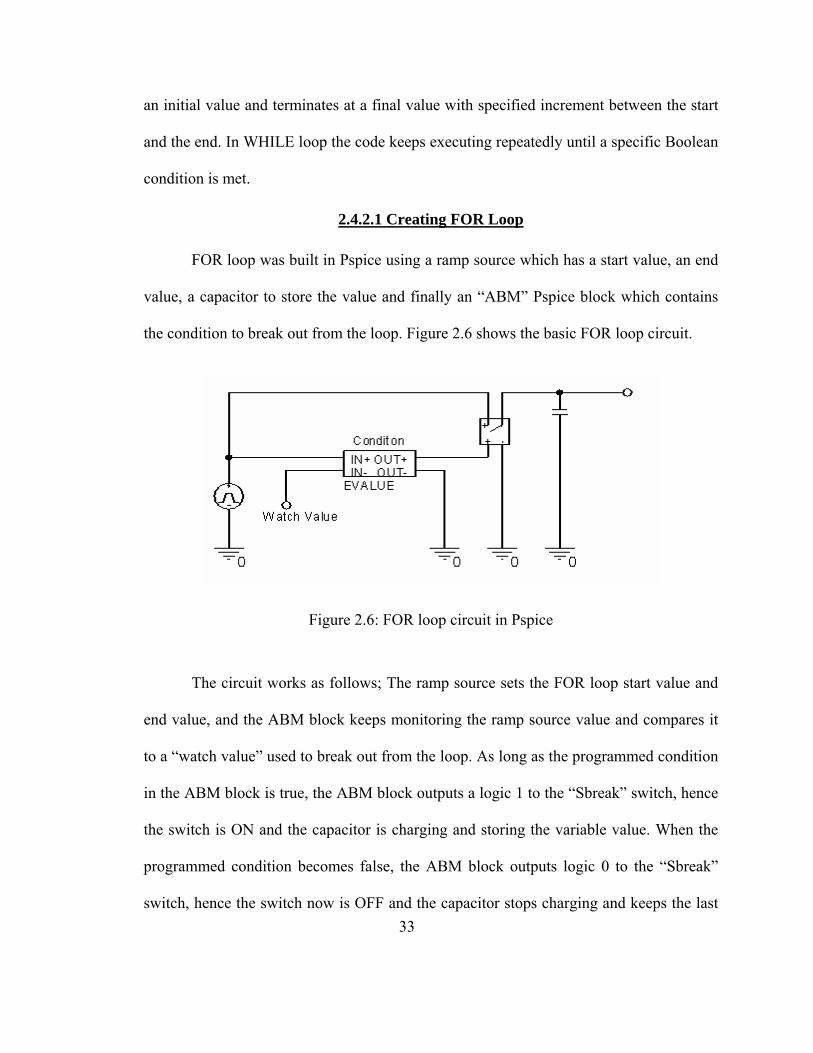
2.4.2.1 Creating FOR Loop....................................................................... 33
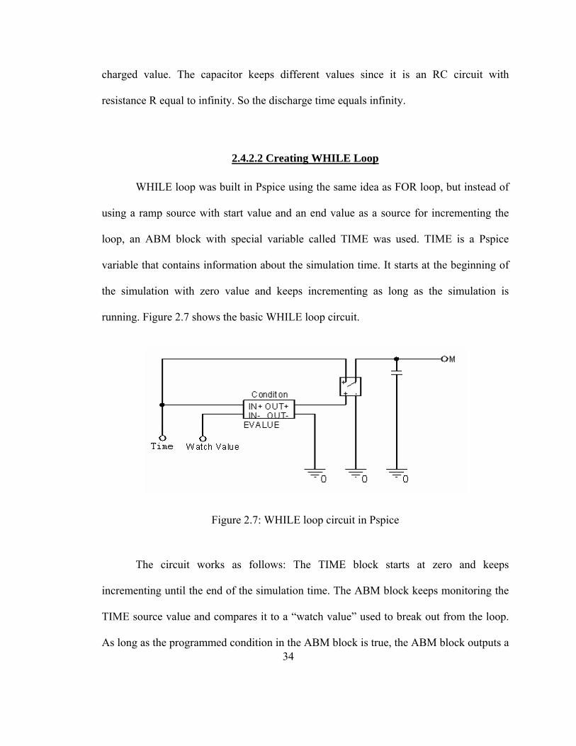
2.4.2.2 Creating WHILE Loop ................................................................. 34
2.5 Developing System Architecture ............................................................................ 35
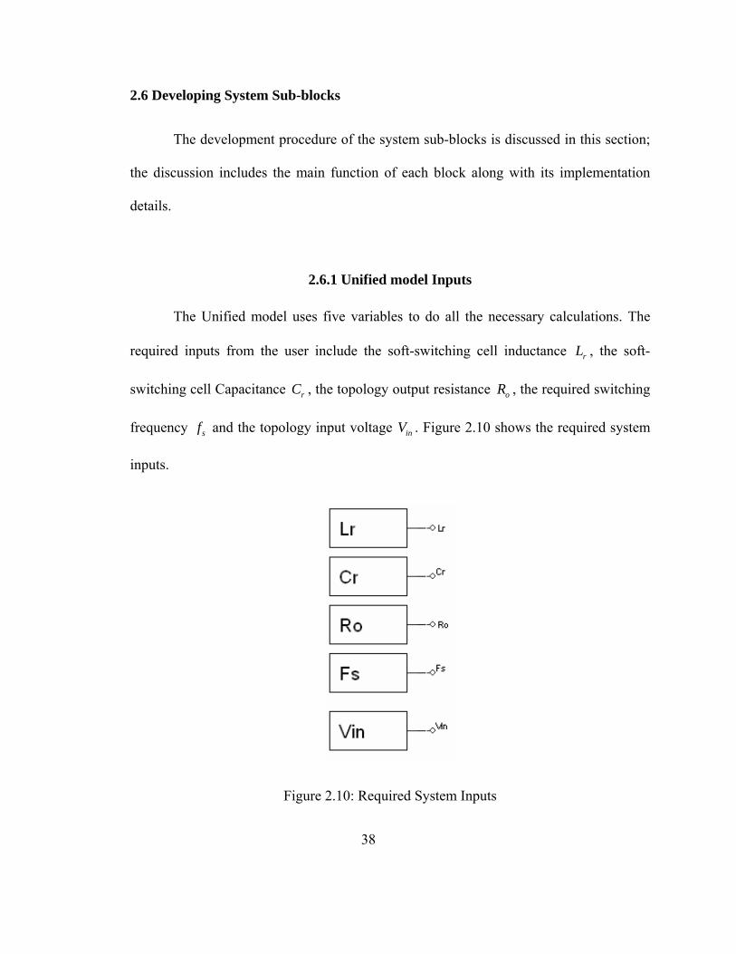
2.6 Developing System Sub-blocks .............................................................................. 38
2.6.1 Unified model Inputs ........................................................................... 38
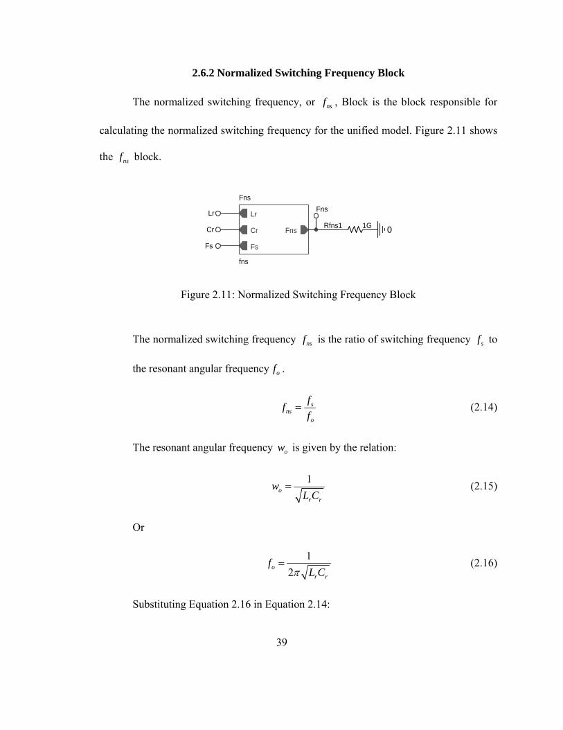
2.6.2 Normalized Switching Frequency Block ............................................. 39
2.6.3 Quality Factor & Characteristics Impedance Block “QZ Block”........ 43
2.6.4 Beta, Gamma and Alpha Block “BG Block”....................................... 47
2.6.4.1 Building Inverse Sine function in Pspice...................................... 51
2.6.5 Error Block “ERR Block”.................................................................... 56
2.6.6 Steady-State Gain Solution Block “SOL Block”................................. 59
2.6.6.1 FOR Loop with Breakout capability............................................. 60
viii
CHAPTER 3: UNIFIED MODEL APPLICATIONS..................................................... 65
3.1 Introduction............................................................................................................. 65
3.2 Generating LrI and CrV steady-state waveform........................................................ 66
3.3 Generating the State-Plane Diagram....................................................................... 75
3.4 Feedback Design..................................................................................................... 79
3.4.1 Detecting changes in switching frequency .......................................... 80
3.4.2 Modified SOL block ............................................................................ 83
3.5 Unified Model for common DC-DC converters families ....................................... 86
3.5.1 Unified Model for Boost converter family .......................................................... 86
3.5.2 Unified Model for Buck-Boost converter family................................................. 89
3.5.3 Selecting between different topologies................................................................ 91
CHAPTER 4 CONCLUSION.......................................................................................... 93
4.1 Summary ................................................................................................................. 93
4.2 Future work............................................................................................................. 94
REFERENCES ................................................................................................................. 95
ix

LIST OF FIGURES
Figure 1.1: Switching-Cells: (a) Conventional Cell ........................................................... 7
Figure 1.1: Switching-Cells: (b) ZVS-QRC Cell................................................................ 7
Figure 1.1: Switching-Cells: (c) ZCS-QRC Cell ................................................................ 7
Figure 1.1: Switching-Cells: (d) ZVS-QSW CV Cell ........................................................ 7
Figure 1.1: Switching-Cells: (e) ZCS-QSW CC Cell, ........................................................ 7
Figure 1.1: Switching-Cells: (f) ZVT-PWM Cell............................................................... 7
Figure 1.1: Switching-Cells: (g) ZCT-PWM Cell .............................................................. 7
Figure 1.2: The Conventional DC-DC Converters: (a) Buck ........................................... 12
Figure 1.2: The Conventional DC-DC Converters: (b) Boost .......................................... 12
Figure 1.2: The Conventional DC-DC Converters: (c) Buck-Boost................................. 12
Figure 1.2: The Conventional DC-DC Converters: (d) Cuk............................................. 12
Figure 1.2: The Conventional DC-DC Converters: (e) Zeta............................................. 12
Figure 1.2: The Conventional DC-DC Converters: (f) Sepic ........................................... 12
Figure 1.3: The Generalized ZCS-QRC Switching Cell with Uni-directional Switch..... 13
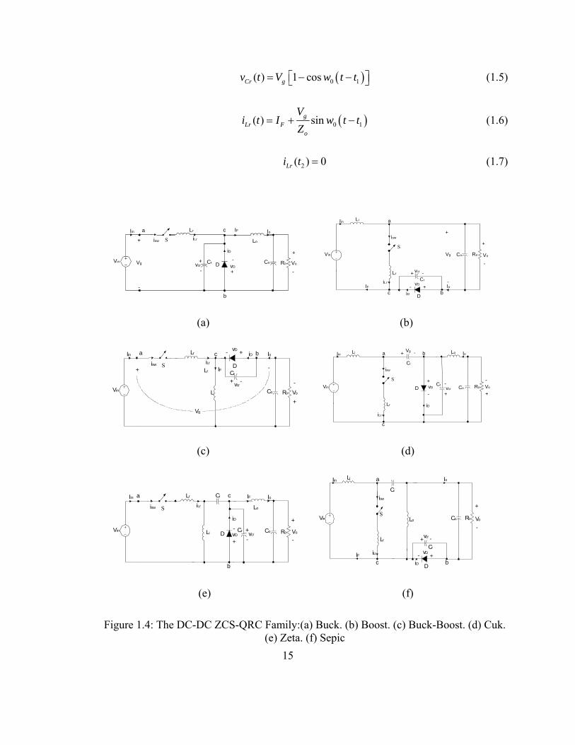
Figure 1.4: The DC-DC ZCS-QRC Family:(a) Buck ....................................................... 15
Figure 1.4: The DC-DC ZCS-QRC Family: (b) Boost. .................................................... 15
Figure 1.4: The DC-DC ZCS-QRC Family: (c) Buck-Boost ........................................... 15
Figure 1.4: The DC-DC ZCS-QRC Family: (d) Cuk........................................................ 15
Figure 1.4: The DC-DC ZCS-QRC Family: (e) Zeta ....................................................... 15
Figure 1.4: The DC-DC ZCS-QRC Family: (f) Sepic ...................................................... 15
x

Figure 1.5: Main ZCS-QRC switching cell waveforms.................................................... 16
Figure 1.6: The equivalent circuits for: (a) Mode 1.......................................................... 19
Figure 1.6: The equivalent circuits for: (b) Mode 2.......................................................... 19
Figure 1.6: The equivalent circuits for: (c) Mode 3.......................................................... 19
Figure 1.6: The equivalent circuits for: (d) Mode 4.......................................................... 19
Figure 1.7a: DC voltage conversion ratio characteristics for ZCS-QRC Buck ................ 22
Figure 1.7b: DC voltage conversion ratio characteristics for ZCS-QRC Boost ............... 22
Figure 1.7c: DC voltage conversion ratio characteristics for ZCS-QRC Buck-Boost, Cuk,
Zeta, and Sepic.......................................................................................................... 23
Figure 1.7d: DC voltage conversion ratio characteristics for The Minimum Allowed Duty
Ratio for the ZCS-QRC Boost .................................................................................. 23
Figure 2.1: Unified Steady-State Model Flow-chart......................................................... 26
Figure 2.2: ZCS-QRC buck unified equation solution Flow-chart................................... 29
Figure 2.3: ZCS-QRC buck steady-state waveforms using MATLAB ............................ 30
Figure 2.5: Creating variables in Pspice ........................................................................... 32
Figure 2.6: FOR loop circuit in Pspice ............................................................................. 33
Figure 2.7: WHILE loop circuit in Pspice ........................................................................ 34
Figure 2.8: System Architecture idea................................................................................ 36
Figure 2.9: System Architecture Implementation in Pspice ............................................. 37
Figure 2.10: Required System Inputs................................................................................ 38
Figure 2.11: Normalized Switching Frequency Block ..................................................... 39
Figure 2.12: Normalized Switching Frequency Block flowchart ..................................... 41
Figure 2.13: Pspice implementation of nsf Block............................................................. 41
xi

Figure 2.14: Pspice Simulation results for nsf Block........................................................ 42
Figure 2.15: Quality Factor & Characteristics Impedance Block..................................... 43
Figure 2.16: Quality Factor and the Characteristics Impedance QZ block flowchart ..... 45
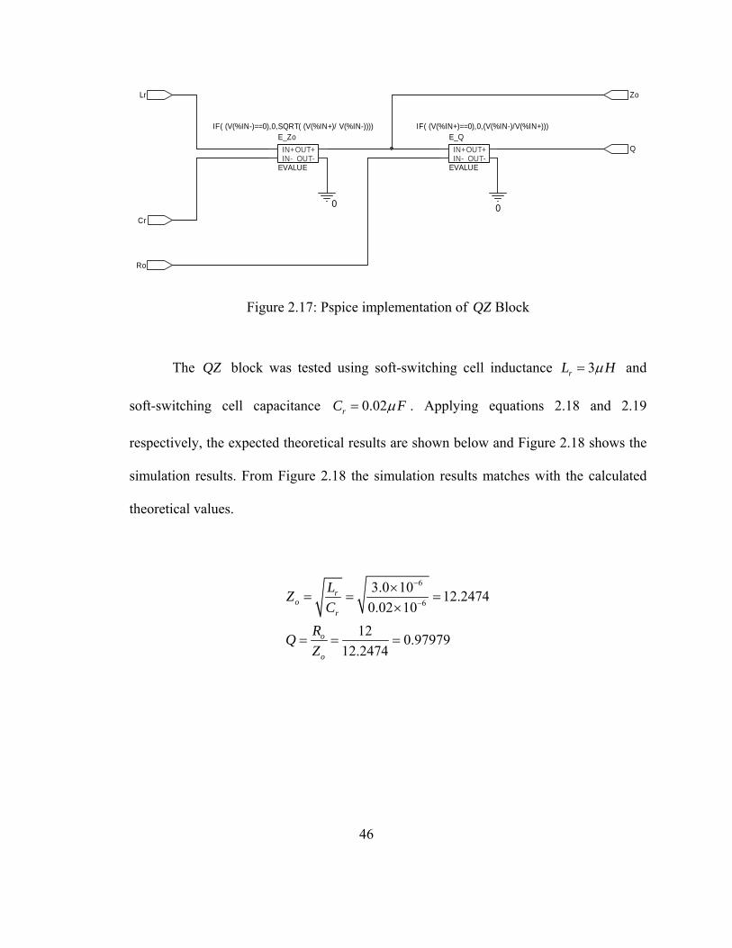
Figure 2.17: Pspice implementation of QZ Block............................................................ 46
Figure 2.18: Pspice Simulation results for nsf Block........................................................ 47
Figure 2.19: Alpha, Beta and Gamma Block.................................................................... 47
Figure 2.20: Alpha, Beta and Gamma block flowchart .................................................... 50
Figure 2.21: Maclaurin series approximation versus actual 1SIN − function ..................... 53
Figure 2.22: 1SIN − block flowchart................................................................................... 54
Figure 2.23: Pspice implementation of BG Block............................................................ 55
Figure 2.24: Error Block................................................................................................... 56
Figure 2.25: The ERR block flowchart............................................................................. 58
Figure 2.26: Pspice implementation of the ERR Block.................................................... 59
Figure 2.27: The Steady-State Gain Solution Block......................................................... 59
Figure 2.28 Basic implementation of SOL Block structure............................................. 61
Figure 2.29 Error Signal Behavior.................................................................................... 62
Figure 2.30 SOL Block with a latch circuit ..................................................................... 63
Figure 2.31 SOL Block with a latch circuit outputs ......................................................... 64
Figure 3.1: LrI and CrV steady-state waveform Block........................................................ 66
Figure 3.2: DRW block flowchart .................................................................................... 68
Figure 3.3: 1MODE Pspice block ..................................................................................... 69
Figure 3.4: 2MODE Pspice block..................................................................................... 70
Figure 3.5: 3MODE Pspice block..................................................................................... 71 xii
Figure 3.6: 4MODE Pspice block..................................................................................... 72
Figure 3.7: All Modes summation Pspice block............................................................... 73
Figure 3.8: Finding time intervals Pspice block ............................................................... 74
Figure 3.9: LrI and CrV steady-state waveform ................................................................. 74
Figure 3.10: The Generalized State plane for ZCS-QRC Switching Cell ........................ 75
Figure 3.11: Switching cell state-plane diagram............................................................... 78
Figure 3.12: Closed loop using the unified general model ............................................... 79
Figure 3.13: Frequency change detection circuit.............................................................. 81
Figure 3.14: Frequency change test signal........................................................................ 82
Figure 3.15: Sampling Pulses ........................................................................................... 82
Figure 3.16: Sampled Test Waveform.............................................................................. 82
Figure 3.17 Frequency change detection block output result ........................................... 83
Figure 3.18: Pspice implementation of counter idea ........................................................ 84
Figure 3.19 modified capacitor-counter circuit ................................................................ 85
Figure 3.20 Unified Model step response ......................................................................... 85
Figure 3.21 Error block for the Boost topology................................................................ 88
Figure 3.22 Error block for the Buck-Boost topology...................................................... 91
Figure 3.23 Complete Error block with topology selection.............................................. 92
xiii
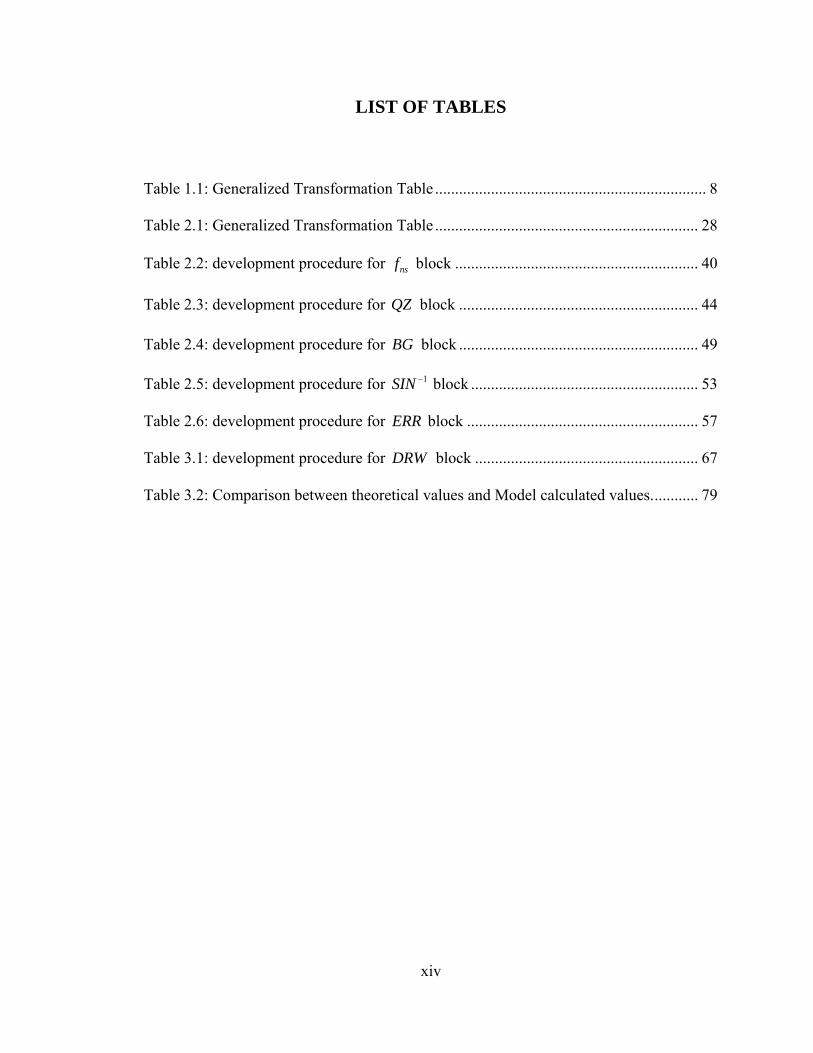
LIST OF TABLES
Table 1.1: Generalized Transformation Table .................................................................... 8
Table 2.1: Generalized Transformation Table .................................................................. 28
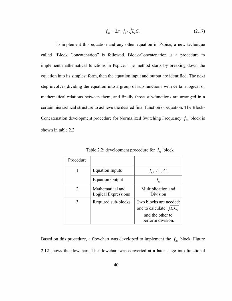
Table 2.2: development procedure for nsf block ............................................................. 40
Table 2.3: development procedure for QZ block ............................................................ 44
Table 2.4: development procedure for BG block ............................................................ 49
Table 2.5: development procedure for 1SIN − block ......................................................... 53
Table 2.6: development procedure for ERR block .......................................................... 57
Table 3.1: development procedure for DRW block ........................................................ 67
Table 3.2: Comparison between theoretical values and Model calculated values............ 79
xiv
1
CHAPTER ONE
INTRODUCTION
1.1 Introduction
The ever increasing demand for DC-DC converters with high power density and
high efficiency introduces many technologies to the power converters industry. One of
those technologies is different soft-switching techniques [1-10]. The main idea behind
soft-switching is to create a resonant condition across the converter main switches to force
the voltage across the switch to decrease to zero before the switch turns ON in what is
knows as Zero Voltage Switching (ZVS), or to force the current passing through the
switch to decrease to zero before the switch turns OFF in what is known as Zero Current
Switching (ZCS).
Soft-switching techniques add many advantages to DC-DC power converters, the
most important is the reduction of switching losses and hence the ability to operate at
higher switching frequencies. Larger switching frequency means smaller magnetic
components size and higher power densities [1-5]. Soft-switching cells achieve those
advantages by employing additional resonant components and auxiliary switches and
diodes.
2
Designing soft-switching cells requires a thorough understanding of the cell
properties and operation, and this in turn requires accurate analysis of the cell during
different main and transition modes of operations at one switching cycle. This is a difficult
and time consuming process, especially when considering the added resonant components
and auxiliary switches and diodes [9,10].
A simpler and a faster way to analyze and find a steady-state solution for soft-
switching cells is by using generalized analysis. Generalized analysis is based on the idea
that soft-switching cells will have the same modes of operation and the same switching
waveforms in spite of cell orientation. Therefore, instead of analyzing switching cells
contained in different converters as a one topology, only the switching cell needs to be
analyzed and the result can be applied to different DC-DC converter families using
transformation tables [2].
In this thesis and based on the generalized equations, a unified simulation model is
derived. The unified steady-state simulation model is a simulation block that covers
common unified soft-switching cell operations [1-16], with defined inputs and outputs,
and can be used in topologies simulation. The user can choose the switching cell type and
can connect the developed simulation model in the desired topology configuration. In
addition to the measurement information that can be obtained from the circuitry around
the unified simulation model, the simulation block includes some additional nodes (other
than the inputs and outputs) that give internal switching cell information, such as
switching voltages and currents. The models is based on mathematical equations, which
3
results in faster simulation times, smaller file size, and greatly minimizes simulation
convergence problems.
The proposed unified simulation model is implemented in Pspice/Orcad®
simulation software [17, 18] to provide a model that can be used as a part of complete
simulation schematic that may include other models in Pspice/Orcad®. Using the
mathematical equations approach to implement the model requires the ability to
implement programming loops and perform instructions in certain sequence. This was the
main challenge in this work because Pspice/Orcad® is not a programming language and
soft –switching cells have complicated set of equations that describe the operation modes.
Chapter 1 generally discusses the generalized equation concept, section 1.2
introduces the switching cell parameters, and section 1.3 shows the generalized
transformation table derivation. To introduce the proposed unified model development
and related development issues and challenges, the zero current switching (ZCS) quasi-
resonant (QRC) unified switching cell [2, 3, 9] was selected. In zero current switching
families, the switches are turned OFF at zero current. To achieve ZCS, the soft-switching
cell utilizes circuit non-idealities like the transformer leakage inductance, junction diode
capacitance and the power switch parasitic capacitance. Chapter 1 gives a complete
analysis of the ZCS-QRC family beginning in Section 1.4 by presenting the ZCS-QRC
Generalized switching cell and it is derived family. Section 1.5 introduces the basic
operation of the ZCS-QRC along with its modes of operation and generalized switching
waveforms, followed by a discussion of the generalized steady-state analysis in section
1.6. Finally section 1.7 shows some design curves for the ZCS-QRC family.

1.2 The Generalized switching cells and their parameters
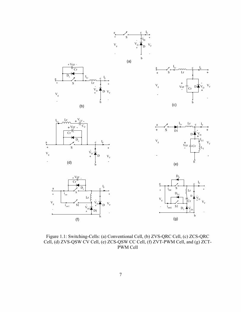
Figure 1.1 shows the generalized switching cells for number of selected families, it
can be noted that those cells have the same modes of operations and thus their analysis can
be generalized. Different converters analysis can be obtained by using different orientation
of any of the cells in Figure 1.1. Using the three terminal notations a, b and c for the
switching cells, the following generalized parameters can be defined as follow:
• The over-all output to input converter gain (M):
o i
in o
V IMV I
= = n
Where :
inV is the converter average input voltage.
oV is the converter average output voltage.
inI is the converter average input current.
oI is the converter average output current.
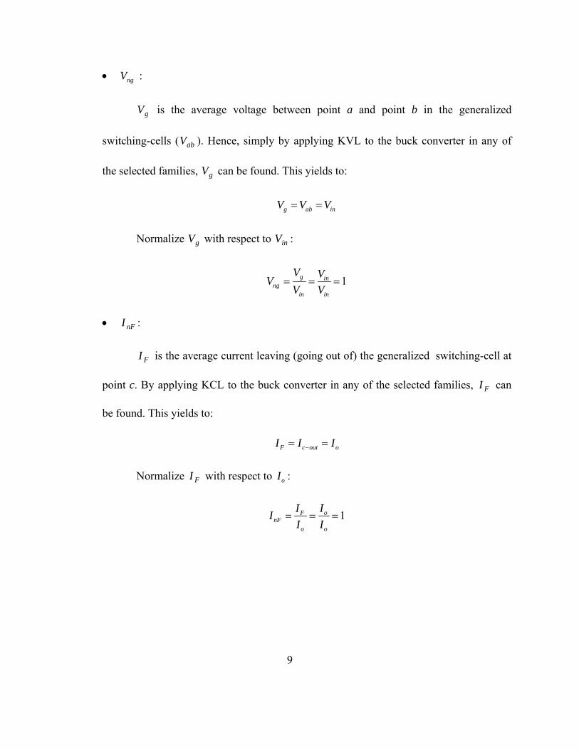
• The normalized cell input voltage ( ): ngV
in
gng V
VV =
Where is the switching-cell average input voltage as show in Figure 1.1. gV
4

• The normalized cell output current ( ) : nFI
FnF
o
III
=
Where FI is the switching-cell average output current as shown in figure 1.1.
• The normalized filter capacitor voltage ( ) : nFV
in
FnF V
VV =
Where is the filter capacitor average voltage. FV
• The normalized filter inductor current ( ) : nTI
TnT
o
III
=
Where TI is the filter inductor average current.
• The normalized cell output average voltage ( ) nbcV
bcnbc
in
VVV
=
Where is the switching cell average output voltage. bcV
5
• The normalized current entering node b in the switching cell ( nbI ) :
bnb
o
III
=
Where bI is the average current entering node b.
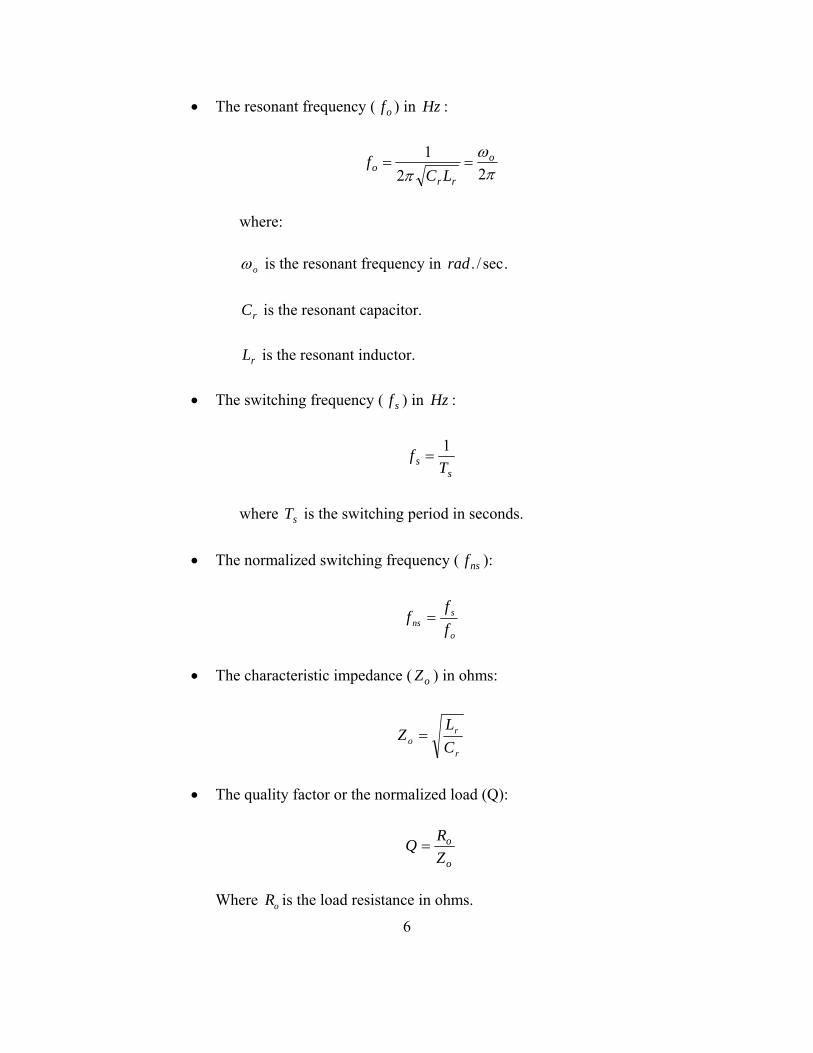
• The resonant frequency ( ) in : of Hz
πω
π 221 o
rro LC
f ==
where:
oω is the resonant frequency in .sec/.rad
rC is the resonant capacitor.
rL is the resonant inductor.
• The switching frequency ( ) in : sf Hz
s
s Tf 1=
where is the switching period in seconds. sT
• The normalized switching frequency ( ): nsf
o
sns f
ff =
• The characteristic impedance ( ) in ohms: oZ
r
ro C
LZ =
• The quality factor or the normalized load (Q):
o
o
ZRQ =
Where oR is the load resistance in ohms.
6
+
-
+
-
a
b
D
+
-
(a)
Vg
S iD
c
VD
IF
VF
(b)
+
-
+
-
a
b
c
D
+ -
+
-
S
Ds
Vg
Lr
ILr IF
VF
VcrCr
VD +
+
-
S
+
-
-
+
-
a
b
c
(c)
D VD
Lr
ILr
Vcr VFCrVg
IF
+
-
a c
S
+
-D
+
-
+
-b
(e)
LT
ILT
CrVcr
LrILr
VF
D1
Vg
VD
IF
VF
+
-
+ -
+
+
-
- +
-
D
a
b
c
S
(d)
CF
VCF
Vcr
IF
VD
Ds
Cr
LrILr
Vg
+
-
S
+
-D
+
-
+
-
a c
b
isw
isw1
(g)
VDVF
S1
Vg
DS1
D1
DS
Lr
Cr
IF
VD1
+
-
S
+
+
-
-
D
+
-
+
-D1
S1
a c
b(f)
isw
isw1VF
VcrCr
Lr
Ds
VD
VD1
IF
Vg
Figure 1.1: Switching-Cells: (a) Conventional Cell, (b) ZVS-QRC Cell, (c) ZCS-QRC Cell, (d) ZVS-QSW CV Cell, (e) ZCS-QSW CC Cell, (f) ZVT-PWM Cell, and (g) ZCT-
PWM Cell
7

1.3 The generalized Transformation Table
A complete set of converters can be obtained by using the various orientations of
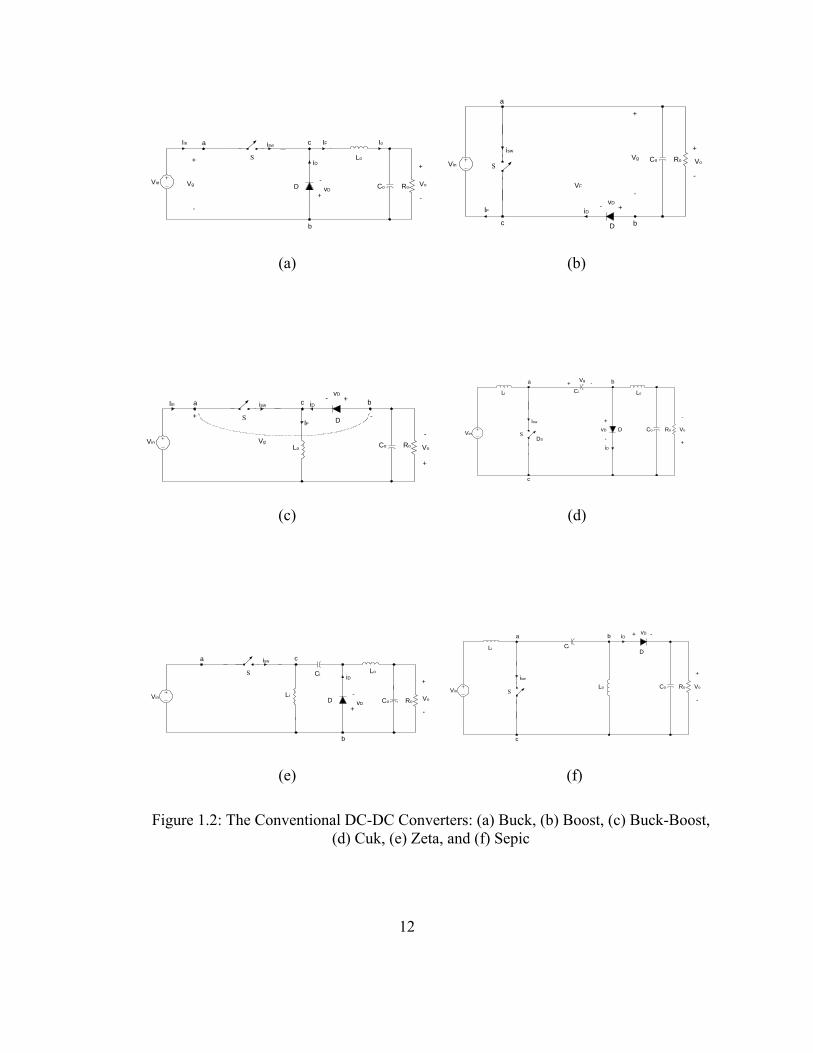
the generalized three terminal cells shown in Figure 1.1. Figure 1.2 shows the common
DC-DC converters, namely, the buck, boost, buck-boost, cuck, zeta, and sepic. The
derivation of the generalized transformation for the above converters can be explained in
this section by choosing the buck converter as an example. The generalized transformation
table is given in Table 1.1. It can be shown that this table is general and can be applied to
all cells in Figure 1.1.
Table 1.1: Generalized Transformation Table
Normalized
Parameters
Buck Boost Buck -Boost, Cuk, Zeta, and
Sepic
ngV , nFI 1 M 1+M
nFV , , nbI nTI 1-M 1 1
nbcV -M 1-M -M
The buck converter is shown is part (a) of figure 1.2, the derivation for the
generalized parameters for the buck converter will be as following:
8
• : ngV
gV is the average voltage between point a and point b in the generalized
switching-cells ( ). Hence, simply by applying KVL to the buck converter in any of
the selected families, can be found. This yields to:
abV
gV
g ab inV V V= =
Normalize with respect to : gV inV
1g inng
in in
V VVV V
= = =
• : nFI
FI is the average current leaving (going out of) the generalized switching-cell at
point c. By applying KCL to the buck converter in any of the selected families, can
be found. This yields to:
FI
F c out oI I I−= =
Normalize with respect to FI oI :
1oFnF
o o
IIII I
= = =
9
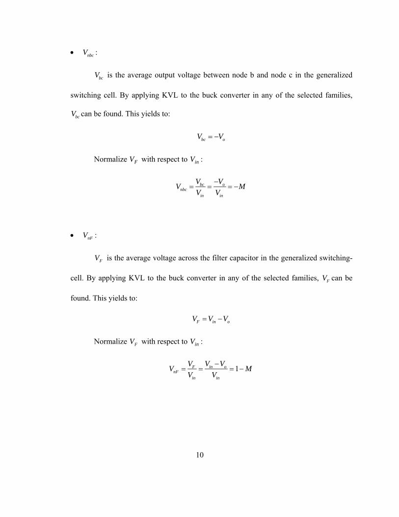
• : nbcV
bcV is the average output voltage between node b and node c in the generalized
switching cell. By applying KVL to the buck converter in any of the selected families,
can be found. This yields to: bcV
bc oV V= −
Normalize with respect to : FV inV
bc onbc
in in
V VV MV V
−= = = −
• : nFV
FV is the average voltage across the filter capacitor in the generalized switching-
cell. By applying KVL to the buck converter in any of the selected families, can be
found. This yields to:
FV
F inV V Vo= −
Normalize with respect to : FV inV
1in oFnF
in in
V VVV MV V
−= = = −
10
• : nbI
bI is the average current entering the generalized switching-cell at point b. By
applying KCL to the buck converter in any of the selected families, can be found. This
yields to:
bI
11
n b b in o iI I I− I= = −
Normalize with respect to bI oI :
1b o innb
o o
I I II MI I
−= = = −
• : nTI
TI is the average current passes through the filter inductor in generalized
switching-cell. By applying KCL to the buck converter in Figure 3.9(d), can be
found. This yields to:
TI
T o inI I I= −
Normalize with respect toTI oI :
1o inTnT
o o
I III MI I
−= = = −
By doing the same derivation for the other converters types, the results will be as
shown in Table 1.1.
Vin
+
-
Vg
S
+
-vD
IF
iD
iswa
b
c
D Co
Lo
Ro
+
-
Vo
IoIin
+
-
Vg
IF
a
+
vD
iDc
S
isw
VF
-
bD
VinCo Ro
+
-
Vo
(a) (b)
+ -
Vg
SIF
iswa c +- vD
iD b
D
Vin Co RoLo
+
-
Vo
Iin
a
c
Vin S
isw
DS
Ro
+
-
Vo
+
vD
iD-
b
D Co
LoLi
+ -Vg
Ci
(c) (d)
Vin
S
iswa c
Co
Lo
Ro
+
-
Vo
+
-vD
iD
b
DLi
Ci
a
c
Vin S
isw
b
Lo
Li Ci
Ro
-
+
VoCo
+ vDiD -
D
(e) (f)
Figure 1.2: The Conventional DC-DC Converters: (a) Buck, (b) Boost, (c) Buck-Boost, (d) Cuk, (e) Zeta, and (f) Sepic
12
1.4 ZCS-QRC Generalized Switching Cell and derived family
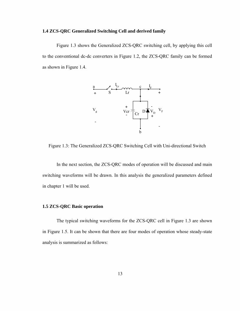
Figure 1.3 shows the Generalized ZCS-QRC switching cell, by applying this cell
to the conventional dc-dc converters in Figure 1.2, the ZCS-QRC family can be formed
as shown in Figure 1.4.
+
+
-
S
+
-
-
+
-
a
b
c
D VD
Lr
ILr
Vcr VFCr
Vg
IF
Figure 1.3: The Generalized ZCS-QRC Switching Cell with Uni-directional Switch
In the next section, the ZCS-QRC modes of operation will be discussed and main
switching waveforms will be drawn. In this analysis the generalized parameters defined
in chapter 1 will be used.
1.5 ZCS-QRC Basic operation
The typical switching waveforms for the ZCS-QRC cell in Figure 1.3 are shown
in Figure 1.5. It can be shown that there are four modes of operation whose steady-state
analysis is summarized as follows:
13
It is assumed that before 0tt = , was OFF and was ON to carry . The
resonant inductor was currying no current and the resonant capacitor voltage was
zero.
S D nFI
rL rC
Mode 1: , starts when is turned ON while is ON, which cause
to charge up linearly until the current through it becomes equal to at
][ 1ttto ≤≤ S D
rL nFI 1tt =
causing to Turn OFF. The equivalent circuit for this mode is shown in Figure 1.6. The
mathematical equation for this mode is as follow (Knowing and
D
0( ) 0Crv t = 0( ) 0Lri t = ):
( ) 0crv t = (1.1)
0( ) ( )gLr
r
Vi t t t
L= − (1.2)
1( ) 0Crv t = (1.3)
1( )Lr Fi t I= (1.4)
Mode 2: , starts when turns OFF while is ON causing a resonant
stage between and to start until the current through drops to zero at
][ 21 ttt ≤≤ D S
rC rL rL 2tt =
causing to turn OFF at zero current (Soft-switching). The equivalent circuit for this
mode is shown in Figure 1.6. The mathematical equation for this mode is as follow:
S
14
( )0 1( ) 1 cosCr gv t V w t t= − −⎡ ⎤⎣ ⎦ (1.5)
(0 1( ) singLr F
o
Vi t I w t t
Z)= + − (1.6)
2( ) 0Lri t = (1.7)
+
-
Vg
S
+
+-
-vcr vD
IF
iD
isw
a
b
c
DCrVin
Lo
Co Ro Vo
IoIin
+
-
iLr
Lr
+
-
Vg
S
+
+
-
-
vcr
IFiLr
iD
isw
a
bc
Lr
D
Cr
Ro
Io
VoCo
+
-
Iin Li
Vin
vD
(a) (b)
+ -
Vg
S
+
+
-
-
vcr
vD
iLrisw
a bc
DCr
IF
iD
Co Ro Vo
Io
+
-LVin
Iin
Lr
Lr
S
+
+ -
-vcrvD
iLr
iD
isw
a b
c
Lr
DCr Ro VoCo
+
-
Iin Li
Vin
Lo IoVg+ -
Ci
(c) (d)
S
+
+ -
-vcrvD
IFiLr
iD
isw
a
b
cLr
D CrVin
Lo
Co Ro Vo
IoIin
+
-Li
Ci
S
+
+
-
-
vcr
vDIF iLr
iD
isw
a
bc
Lr
D
Cr
Ro
Io
VoCo
+
-
Iin Li
Vin Lo
Ci
(e) (f)
Figure 1.4: The DC-DC ZCS-QRC Family:(a) Buck. (b) Boost. (c) Buck-Boost. (d) Cuk. (e) Zeta. (f) Sepic
15
t2 t3t0 t0+Ts
t
DS
iLr
IF
t1
vCr
IF+Vg/Zo
2Vg
tCr-ptLr-p
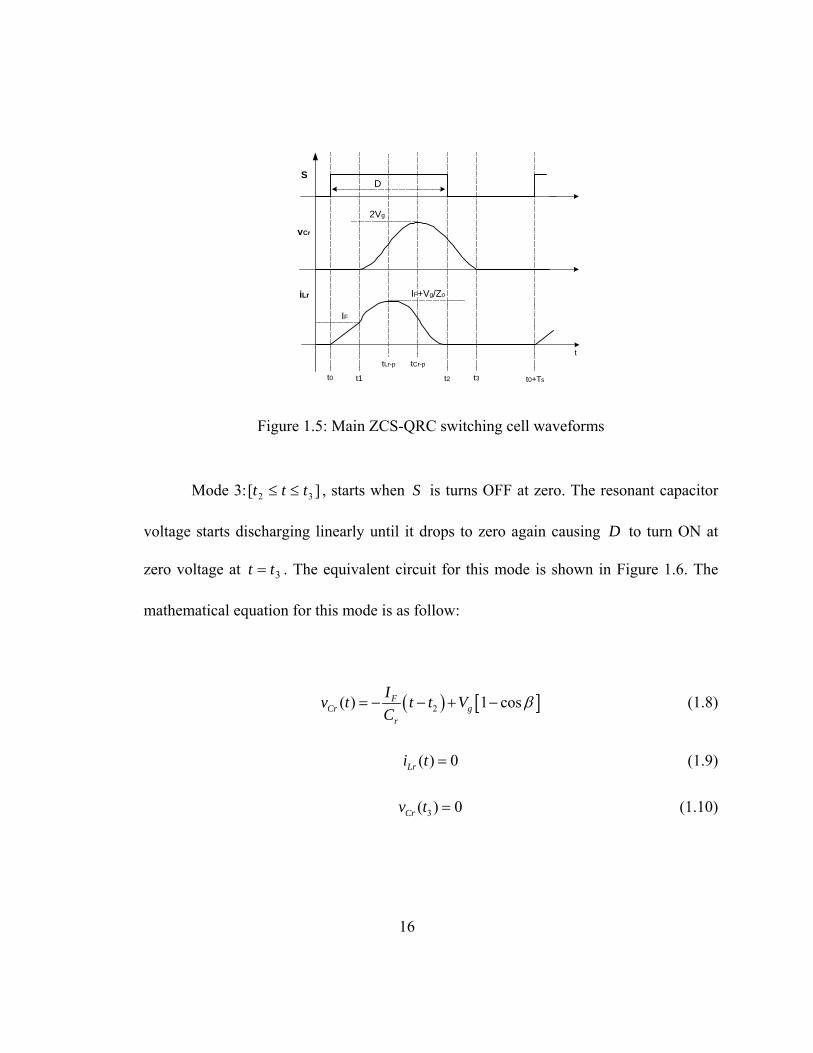
Figure 1.5: Main ZCS-QRC switching cell waveforms
Mode 3: , starts when is turns OFF at zero. The resonant capacitor
voltage starts discharging linearly until it drops to zero again causing to turn ON at
zero voltage at . The equivalent circuit for this mode is shown in Figure 1.6. The
mathematical equation for this mode is as follow:
][ 32 ttt ≤≤ S
D
3tt =
( ) [2( ) 1 cosFCr g
r
Iv t t t VC
]β= − − + − (1.8)
( ) 0Lri t = (1.9)
3( ) 0Crv t = (1.10)
16

Mode 4: , mode 4 is a steady-state mode and nothing happen on it
until is turned ON again to start the next switching cycle. The equivalent circuit for
this mode is shown in Figure 1.6. The mathematical equation for this mode is as follow:
][ 3 so Tttt +≤≤
S
( ) 0Lri t = (1.11)
3( ) 0Crv t = (1.12)
1.6 Generalized Steady-State Analysis
From the modes of operations discussed in Section 1.5 generalized parameters can
be defined and generalized equations can be derived. Section 1.6.1 defines the
generalized parameters and based on them the generalized gain equation is derived in
section 1.6.2. The generalized ZCS condition is discussed in 1.6.3 and finally generalized
peak values for the switching cell inductor current and the switching cell capacitor
voltage is discussed in section 1.6.4.
1.6.1 Generalized Intervals Equations
To simplify the analysis, the following time intervals are defined:
)( 01 tto −= ωα
)( 12 tto −= ωβ
)( 23 tto −= ωδ
))(( 30 tTt so −+=ωη
17
These intervals can be derived as follows:
• From Equations (1.2) and (1.4) :
1 0( ) o Fo
g
Z It tV
α ω= − =
By using the normalized parameters defined in Section 1.2:
1 0( ) nFo
ng
MIt tQV
α ω= − = (1.13)
• From Equations (1.6) and (1.7) :
12 1( ) sin ( nF
ong
)MIt tQV
β ω −= − = − (1.14)
• From Equations (1.8) and (1.10) :
3 2( ) (1 cosngo
nF
QVt t
MI)γ ω= − = − β (1.15)
• From Figure 1.5 and the above intervals :
0 32(( ) )o s
ns
t T tfπδ ω= + − = − −α β γ− (1.16)
18
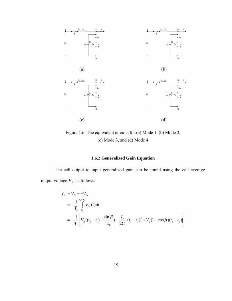
+
-
Vg
IFiLr
iD
a
b
cLr
S
+
-vcrCr
vD+
-D
+
-
Vg
IFiLr
iD
a
b
cLr
S
+
-vcrCr
vD+
-D
(a) (b)
+
-
Vg
IFiLr
iD
a
b
cLr
S
+
-vcrCr
vD+
-D
+
-
Vg
IFiLr
iD
a
b
cLr
S
+
-vcrCr
vD+
-D
(c) (d)
Figure 1.6: The equivalent circuits for:(a) Mode 1, (b) Mode 2,
(c) Mode 3, and (d) Mode 4
1.6.2 Generalized Gain Equation
The cell output to input generalized gain can be found using the cell average
output voltage as follows: FV
0
0
22 1 3 2 3 2
0
1 ( )
1 sin (( ) ) ( ) (1 cos )( )2
s
bc D Cr
t T
Crs t
Fg g
s r
V V V
v t dtT
IV t t t t V t tT w C
β β
+
= = −
= −
⎡ ⎤= − − − − − + − −⎢ ⎥
⎣ ⎦
∫
19
By using the normalized parameters defined in Section 1.2, we will have:
2 ( sin cos2 2
ns nFnbc ng
f MIV VQ
)γ β γ β γ βπ⎡ ⎤
= − + − −⎢ ⎥⎣ ⎦
(1.17)
By substituting for the generalized parameters ( , , and ) from Table
1.1 in Equation (1.17), we will have the gain equation for each converter in the family.
nFV ngV nFI
1.6.3 Generalized ZCS Condition
In order to achieve ZCS, which means that S must be turned OFF at zero current
condition. This condition can be noticed from Figure 1.5 after 2tt = when the resonant
inductor (switch) current drops to zero and before 3tt = when the resonant capacitor
voltage drops to zero causing to conduct and the resonant inductor current starts
charging again. The generalized condition to achieve zero-current switching can be
expresses as follows:
D
)()(2)( γβαπβα ++≤≤+ Dfns
(1.18a)
Which limit the minimum and maximum value of the duty ratio to:
)(2min βαπ
+= nsfD (1.18b)
)(2max γβαπ
++= nsfD (1.18c)
20
1.6.4 Generalized peak resonant Inductor Current and capacitor voltage
The peak resonant inductor current or peak switch current occurs at Lr pt t −= when
0 1( )Lr pw t t / 2π− − = . By using Equation (1.6) at Lr pt t −= :
ngnLr P nF
QVI I
M− = + (1.19)
The peak resonant capacitor voltage or peak diode voltage occurs at Cr pt t −= when
0 1( )Cr pw t t π− − = . By using Equation (1.5) at Cr pt t −= :
2nD p nCr p ngV V V− −= = (1.20)
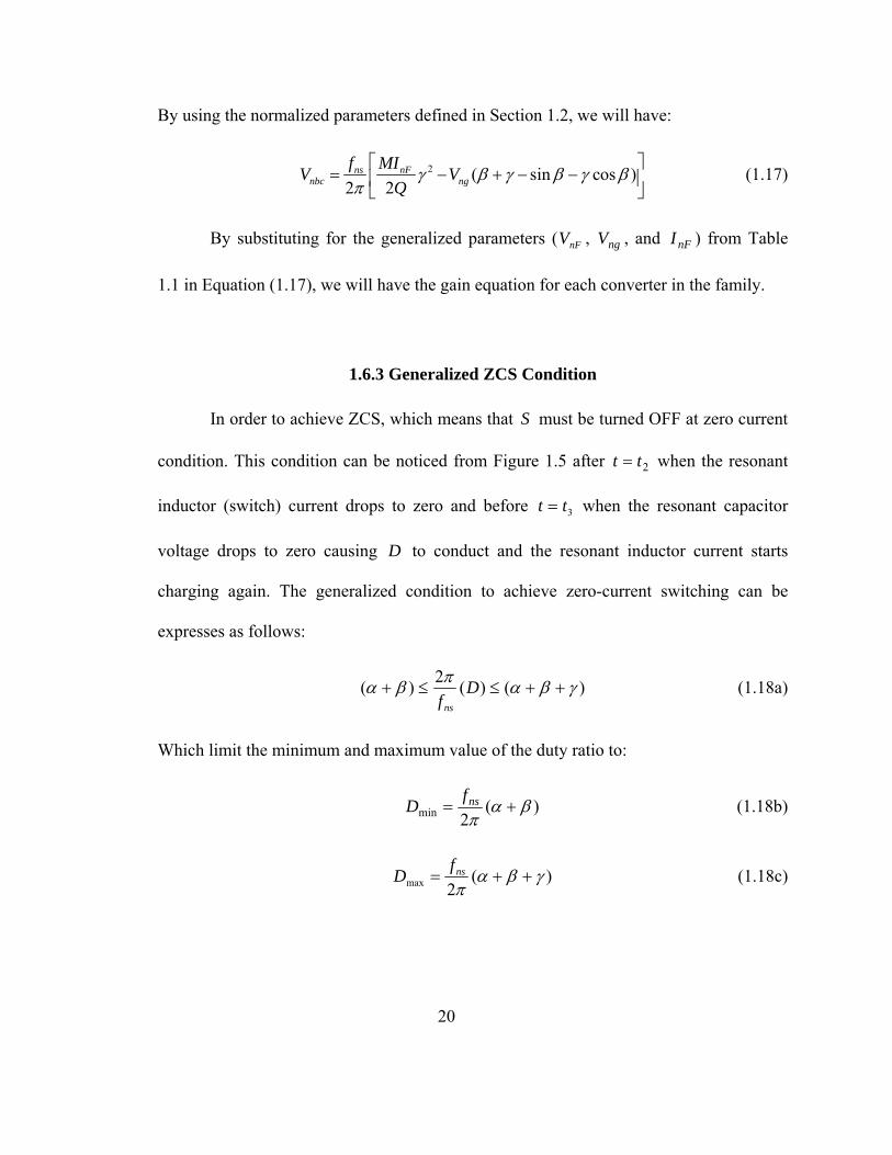
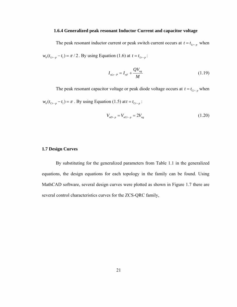
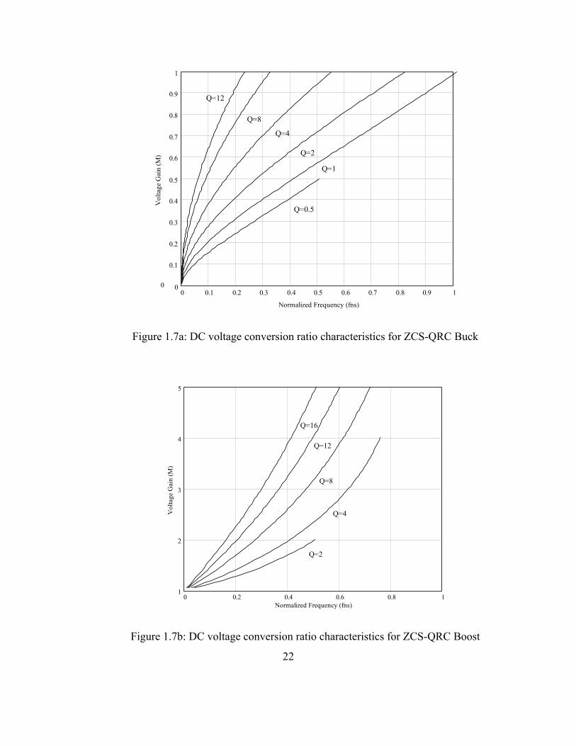
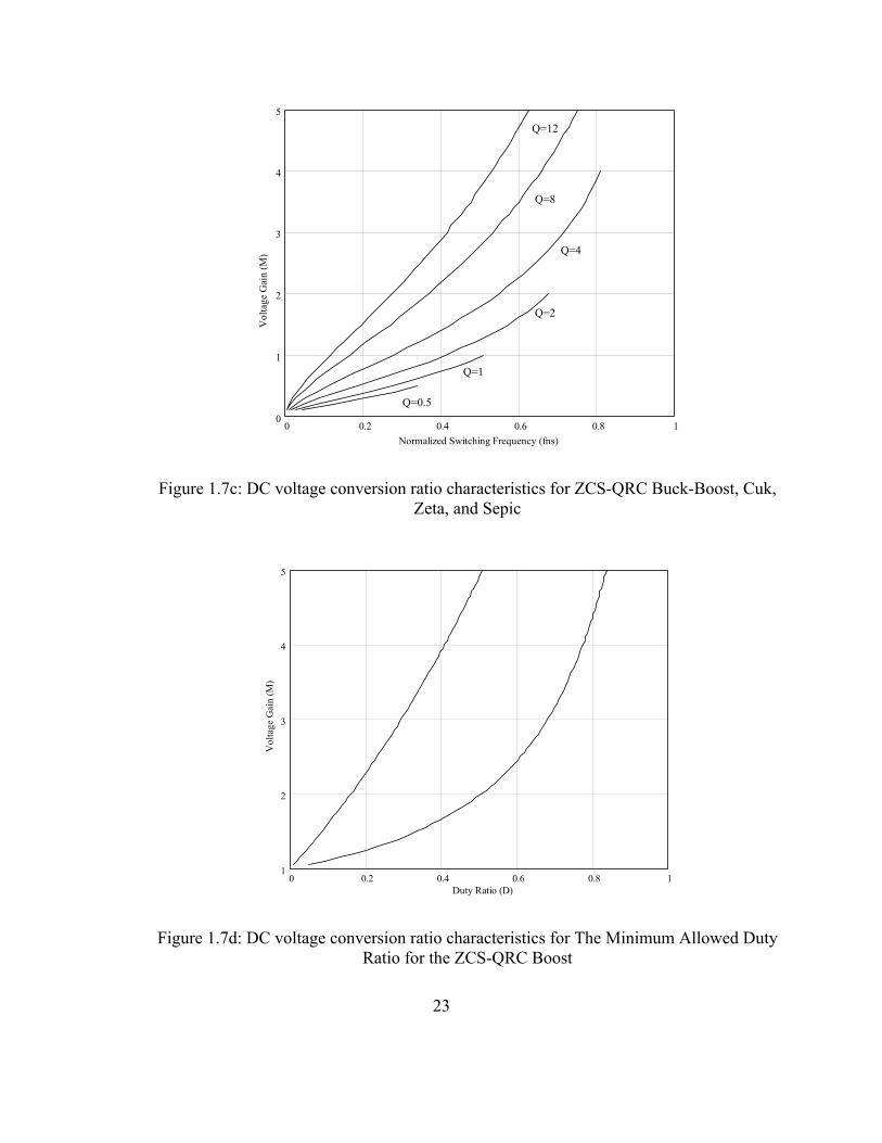
1.7 Design Curves
By substituting for the generalized parameters from Table 1.1 in the generalized
equations, the design equations for each topology in the family can be found. Using
MathCAD software, several design curves were plotted as shown in Figure 1.7 there are
several control characteristics curves for the ZCS-QRC family,
21
0 0.1 0.2 0.3 0.4 0.5 0.6 0.7 0.8 0.9 10
0.1
0.2
0.3
0.4
0.5
0.6
0.7
0.8
0.9
1
Normalized Frequency (fns)
Vol
tage
Gai
n (M
)
0
Q=0.5
Q=1
Q=2
Q=4
Q=8
Q=12
Figure 1.7a: DC voltage conversion ratio characteristics for ZCS-QRC Buck
0 0.2 0.4 0.6 0.8 11
2
3
4
5
Normalized Frequency (fns)
Vol
tage
Gai
n (M
)
Q=16
Q=2
Q=4
Q=8
Q=12
Figure 1.7b: DC voltage conversion ratio characteristics for ZCS-QRC Boost
22
0 0.2 0.4 0.6 0.8 10
1
2
3
4
5
Normalized Switching Frequency (fns)
Vol
tage
Gai
n (M
)
Q=0.5
Q=1
Q=2
Q=4
Q=8
Q=12
Figure 1.7c: DC voltage conversion ratio characteristics for ZCS-QRC Buck-Boost, Cuk, Zeta, and Sepic
0 0.2 0.4 0.6 0.8 11
2
3
4
5
Duty Ratio (D)
Vol
tage
Gai
n (M
)
Figure 1.7d: DC voltage conversion ratio characteristics for The Minimum Allowed Duty Ratio for the ZCS-QRC Boost
23
24
CHAPTER 2
UNIFIED MODEL CONCEPT AND IMPLEMENTATION
2.1 Introduction
The main idea behind the unified model is to have a unified steady-state
simulation model that covers common soft-switching cells and can be used in topologies
simulation. The user chooses the switching cell type and connects the simulation model
to the desired topology configuration. The model provides the user with the internal
switching cell information such as the switching voltage and current in addition to the
regular measurement information that can be obtained from the circuitry around the
unified model. To introduce the proposed unified model concept and related development
issues and challenges, the zero current switching (ZCS) quasi-resonant (QRC) unified
switching cell [4, 5, 6, 8, 9] was selected.
Implementing the unified model in Pspice was not straightforward for the
following two main reasons: First, Pspice is not a programming language, hence it
doesn’t have variables or basic programming elements like “For” or “While” loops, it
only support very basic IF..ELSE function. Second, the final output in Pspice is the result
of object interaction and hence implementing different flow charts is confusing especially
when trying to control the flow of the program and the proper way of communication
between the objects [17-26].
In this chapter a detailed discussion of the unified model concept and
implementation is presented, next section presents the Unified Steady-State Model flow-
chart, Section 2.3 discusses the modified flow-chart for the Zero Current Switching Quasi
Resonant converter ZCS-QRC, the chapter then moves to the implementation of this
flow-chart in Pspice in Section 2.4 by presenting how to build the necessary
programming components for Pspice. Building functional block is Pspice should be done
in certain way Section 2.5 discuss the system architecture in Pspice and finally Section
2.6 shows the detailed implementation of the system blocks in Pspice.
2.2 Unified Steady-State Model Flow-chart
The general flow chart of the unified model is shown in Figure 2.1. The flow
chart explains the basic internal structure of the unified model and the way it works. The
model starts by taking necessary inputs from the user this includes the input voltage, the
switching cell inductance , the switching cell capacitance and the switching
frequency
rL rC
sf as a constant input to the cell or from the closed loop controller. The model
then calculates the normalized switching frequency , thensf characteristic impedance
oZ and the Quality factor Q. Those calculated values are constant values that will be used
at a later stage in the model. Then, the model goes through several iterations, in each
iteration, several sub-equations are evaluated, and the sub-equations final results are
mathematically arranged and stored according to the topology, and subtracted from
previously calculated value. The result of this comparison determines if steady-state
solution is reached or more iterations are still needed. After finding the steady-state
solution, the final stage generates steady-state waveforms of the switching cell.
nsf
25
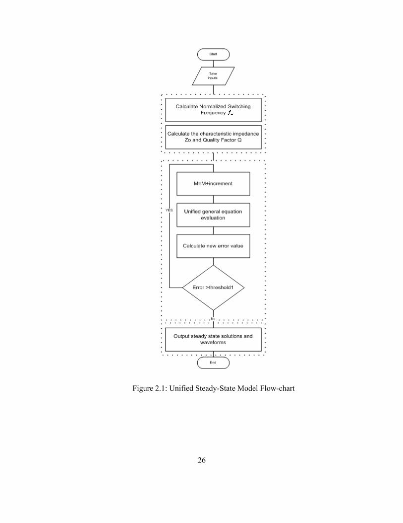
Figure 2.1: Unified Steady-State Model Flow-chart
26
2.3 ZCS-QRC Steady-State Model Flow-chart
The derivation of the generalized gain equation for the zero current switching
(ZCS) quasi-resonant (QRC) switching cell was discussed in details in the previous
chapter. From Section 1.6.2:
2 ( sin cos2 2
ns nFnD ng
f MIV VQ
)γ β γ β γ βπ⎡ ⎤
= − + − −⎢ ⎥⎣ ⎦
(2.1)
Where:
o
in
VMV
= (2.2)
sns
o
fff
= (2.3)
o
o
RQZ
= (2.4)
nF
ng
MIQV
α = (2.5)
1sin ( )nF
ng
MIQV
β −= − (2.6)
(1 cos )ng
nF
QVMI
γ β= − (2.7)
2
nsfπδ α β γ= − − − (2.8)
And the generalized transformation table from Section 1.3 is shown in table 2.1.
27

Table 2.1: Generalized Transformation Table
Normalized
Parameters
Buck Boost Buck -Boost
ngV , nFI 1 M 1+M
nFV , , nbI nTI 1-M 1 1
nbcV -M 1-M -M
Using the ZCS-QRC generalized gain equation 2.1 and the generalized
transformation table 2.1 the generalized gain equation for ZCS-QRC buck converter
becomes:
2 ( sin cos2 2
nsf MMQ
)γ β γ β γ βπ⎡ ⎤
− = − + − −⎢ ⎥⎣ ⎦
(2.9)
Where: MQ
α = (2.10)
1sin ( )MQ
β −= − (2.11)
(1 cos )QM
γ β= − (2.12)
Equation 2.9 is a non-linear equation with the steady-state gain solution M in
both sides of the equation. To simplify the solving algorithm the equation was rearranged
and solved in terms of nsf as shown in equation 2.13.
2
2
( sin cos2
nsMf M
Q)
π
γ β γ β γ β
−=
− + − − (2.13)
28
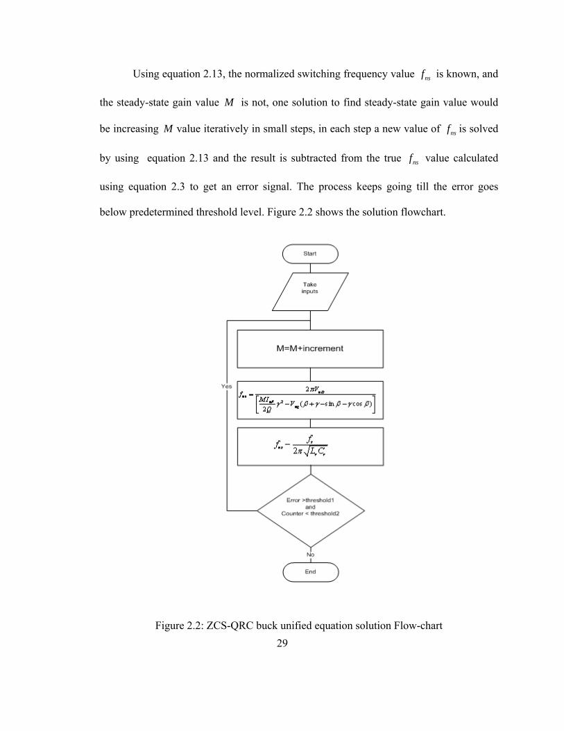
Using equation 2.13, the normalized switching frequency value nsf is known, and
the steady-state gain value M is not, one solution to find steady-state gain value would
be increasing M value iteratively in small steps, in each step a new value of nsf is solved
by using equation 2.13 and the result is subtracted from the true nsf value calculated
using equation 2.3 to get an error signal. The process keeps going till the error goes
below predetermined threshold level. Figure 2.2 shows the solution flowchart.
Figure 2.2: ZCS-QRC buck unified equation solution Flow-chart
29
30
H
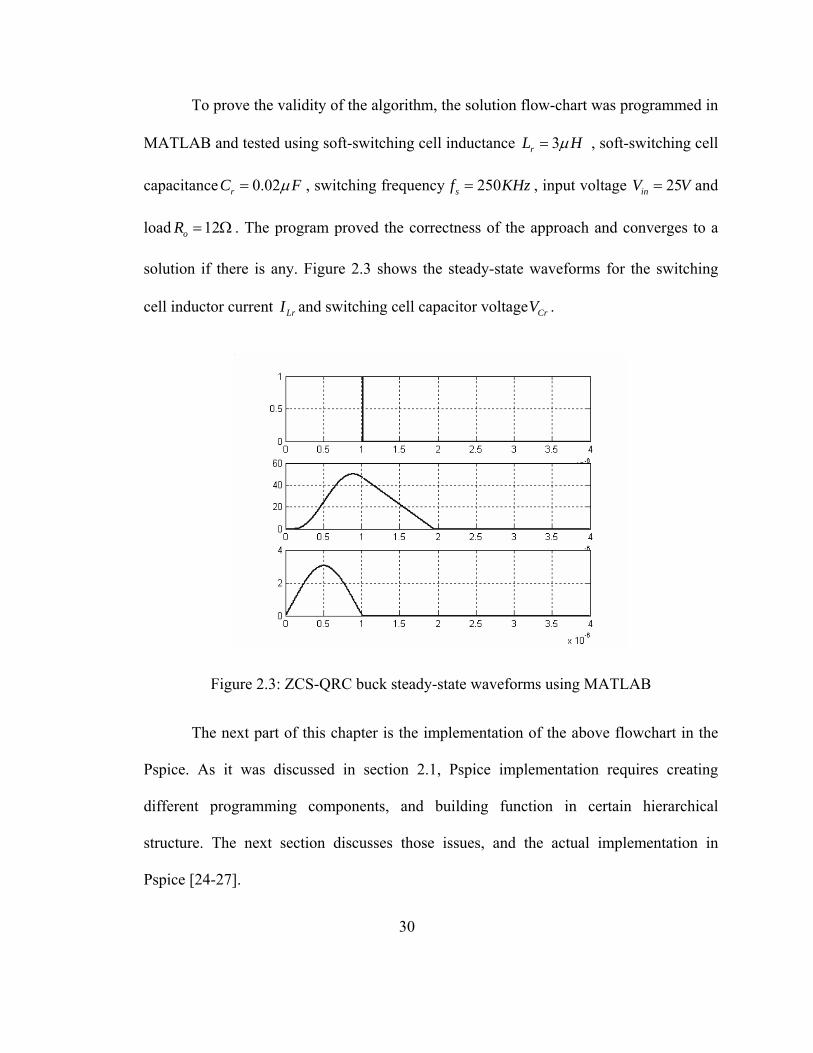
To prove the validity of the algorithm, the solution flow-chart was programmed in
MATLAB and tested using soft-switching cell inductance 3rL µ= , soft-switching cell
capacitance 0.02rC Fµ= , switching frequency 250sf KHz= , input voltage and
load . The program proved the correctness of the approach and converges to a
solution if there is any. Figure 2.3 shows the steady-state waveforms for the switching
cell inductor current
25inV V=
12oR = Ω
LrI and switching cell capacitor voltage . CrV
Figure 2.3: ZCS-QRC buck steady-state waveforms using MATLAB
The next part of this chapter is the implementation of the above flowchart in the
Pspice. As it was discussed in section 2.1, Pspice implementation requires creating
different programming components, and building function in certain hierarchical
structure. The next section discusses those issues, and the actual implementation in
Pspice [24-27].
2.4 Building programming components
To overcome the lack of programming elements in Pspice, necessary
programming tools were developed based on existing Pspice elements. The two most
important elements considered are creating variables and creating loops. Section 2.4.1
presents the implementation of variables in Pspice and section 2.4.2 discusses the
implementation of FOR and WHILE loop in Pspice.
2.4.1 Creating variables in Pspice
Variables are symbols denoting a quantity; Pspice supports a basic type of
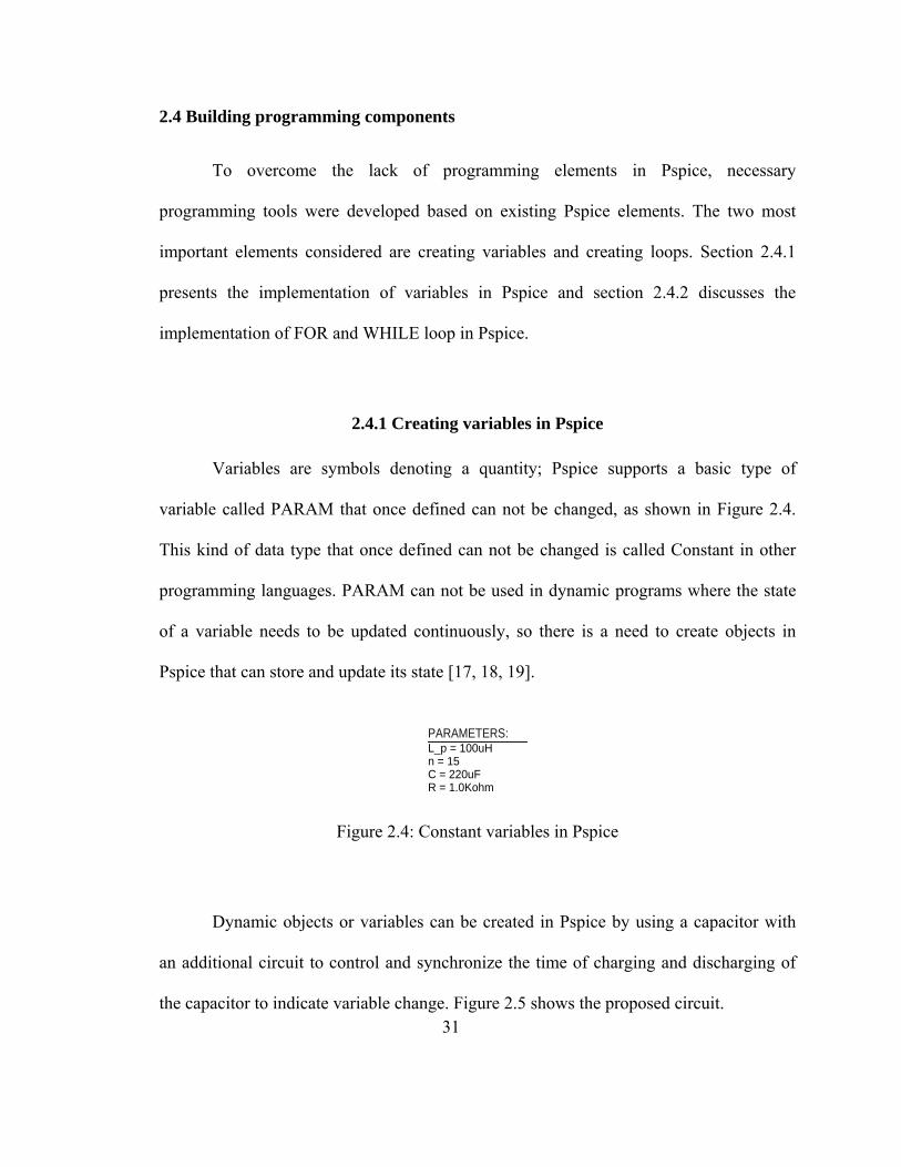
variable called PARAM that once defined can not be changed, as shown in Figure 2.4.
This kind of data type that once defined can not be changed is called Constant in other
programming languages. PARAM can not be used in dynamic programs where the state
of a variable needs to be updated continuously, so there is a need to create objects in
Pspice that can store and update its state [17, 18, 19].
PARAMETERS:L_p = 100uHn = 15C = 220uFR = 1.0Kohm
Figure 2.4: Constant variables in Pspice
Dynamic objects or variables can be created in Pspice by using a capacitor with
an additional circuit to control and synchronize the time of charging and discharging of
the capacitor to indicate variable change. Figure 2.5 shows the proposed circuit. 31
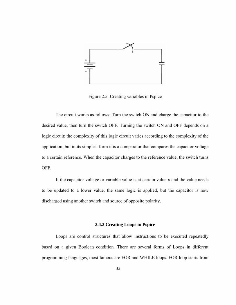
Figure 2.5: Creating variables in Pspice
The circuit works as follows: Turn the switch ON and charge the capacitor to the
desired value, then turn the switch OFF. Turning the switch ON and OFF depends on a
logic circuit; the complexity of this logic circuit varies according to the complexity of the
application, but in its simplest form it is a comparator that compares the capacitor voltage
to a certain reference. When the capacitor charges to the reference value, the switch turns
OFF.
If the capacitor voltage or variable value is at certain value x and the value needs
to be updated to a lower value, the same logic is applied, but the capacitor is now
discharged using another switch and source of opposite polarity.
2.4.2 Creating Loops in Pspice
Loops are control structures that allow instructions to be executed repeatedly
based on a given Boolean condition. There are several forms of Loops in different
programming languages, most famous are FOR and WHILE loops. FOR loop starts from
32
an initial value and terminates at a final value with specified increment between the start
and the end. In WHILE loop the code keeps executing repeatedly until a specific Boolean
condition is met.
2.4.2.1 Creating FOR Loop
FOR loop was built in Pspice using a ramp source which has a start value, an end
value, a capacitor to store the value and finally an “ABM” Pspice block which contains
the condition to break out from the loop. Figure 2.6 shows the basic FOR loop circuit.
Figure 2.6: FOR loop circuit in Pspice
The circuit works as follows; The ramp source sets the FOR loop start value and
end value, and the ABM block keeps monitoring the ramp source value and compares it
to a “watch value” used to break out from the loop. As long as the programmed condition
in the ABM block is true, the ABM block outputs a logic 1 to the “Sbreak” switch, hence
the switch is ON and the capacitor is charging and storing the variable value. When the
programmed condition becomes false, the ABM block outputs logic 0 to the “Sbreak”
switch, hence the switch now is OFF and the capacitor stops charging and keeps the last
33
charged value. The capacitor keeps different values since it is an RC circuit with
resistance R equal to infinity. So the discharge time equals infinity.
2.4.2.2 Creating WHILE Loop
WHILE loop was built in Pspice using the same idea as FOR loop, but instead of
using a ramp source with start value and an end value as a source for incrementing the
loop, an ABM block with special variable called TIME was used. TIME is a Pspice
variable that contains information about the simulation time. It starts at the beginning of
the simulation with zero value and keeps incrementing as long as the simulation is
running. Figure 2.7 shows the basic WHILE loop circuit.
Figure 2.7: WHILE loop circuit in Pspice
34
The circuit works as follows: The TIME block starts at zero and keeps
incrementing until the end of the simulation time. The ABM block keeps monitoring the
TIME source value and compares it to a “watch value” used to break out from the loop.
As long as the programmed condition in the ABM block is true, the ABM block outputs a

35
logic 1 to the “Sbreak” switch, hence the switch is ON and the capacitor is charging and
storing the variable value. When the programmed condition becomes false, the ABM
block outputs logic 0 to the “Sbreak” switch, hence the switch is OFF and the capacitor
stops charging and keeps the last charged value.
2.5 Developing System Architecture
Pspice has a different architecture than conventional programming languages. In
conventional programming languages, the programmer writes a set of lines that compose
certain functionality. The execution of the program or the function starts from the first
line and ends by the last line, so the flow of the program and the direction of execution
are determined by the order of the written lines. On the other hand, Pspice is an
object-based program; the user places several objects in the work space, connects them
together and the final outcome is the result of the interaction of those objects. So
implementing different flowcharts in Pspice requires more effort, especially when trying
to control the flow of the program and the proper communication between objects.
The unified equation was programmed in Pspice using special architecture that
divides the programs into several functions and implements those functions using Pspice
blocks that interact with each other. The unified general equation architecture includes a
main block that passes certain values to other “sub-blocks.” Those sub-blocks then
process the information and update the Main-Block with the new values. Based on those
new values, the Main-Block decides whether to continue solving or to stop when a
steady-state solution is reached. Figure 2.8 shows the system architecture idea.
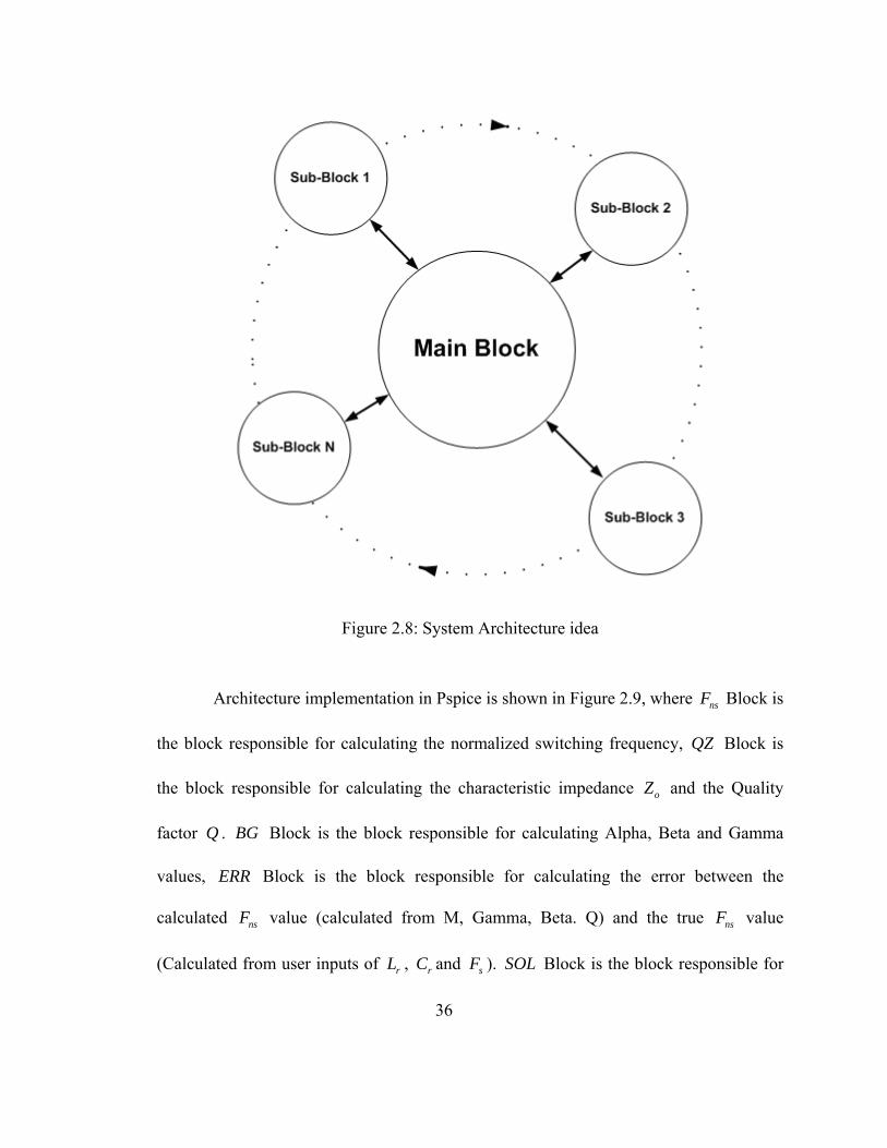
Figure 2.8: System Architecture idea
Architecture implementation in Pspice is shown in Figure 2.9, where Block is
the block responsible for calculating the normalized switching frequency, Block is
the block responsible for calculating the characteristic impedance
nsF
QZ
oZ and the Quality
factor . Q BG Block is the block responsible for calculating Alpha, Beta and Gamma
values, Block is the block responsible for calculating the error between the
calculated value (calculated from M, Gamma, Beta. Q) and the true value
(Calculated from user inputs of , and
ERR
nsF nsF
rL rC sF ). Block is the block responsible for SOL
36
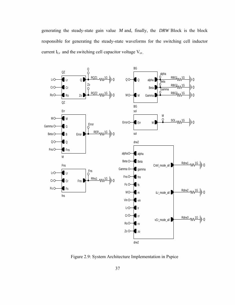
generating the steady-state gain value M and, finally, the Block is the block
responsible for generating the steady-state waveforms for the switching cell inductor
current I
DRW
Lr and the switching cell capacitor voltage Vcr..
M
Rfns1 1G
Rdrw1 1G
M
Ro RBG3 1G
M
0BetaQ
Rdrw3 1G
RBG2 1G
Beta
alpha
Cr
drw2
drw2
lr
m
zo
fns
fs
vin
vCr_mode_all
Cntrl_mode_all
alpha
gamma
iLr_mode_all
Beta
cr
ro
Vin
Gamma
0
Lr
0Beta
Fns
0
Fs
0
FsCr
0
Fns
Fns
fns
Fs
Cr Fns
Lr
Zo
Gamma
Err
M
M
G
B
Q
Fns
Error
M
RBG1 1GQZ
QZ
Lr
Cr
Q
ZoRo
0
0
SOL 1G
Zo
Ro
Gamma
BG
BG
M
Q
Beta
Gamma
alpha
Q
RQZ2 1G
Cr
RQZ1 1G
sol
sol
MErr
Rdrw2 1G
alpha
0
Error Error
0
Q
Fns
0
Lr
RER 1G
Lr
Figure 2.9: System Architecture Implementation in Pspice
37
2.6 Developing System Sub-blocks
The development procedure of the system sub-blocks is discussed in this section;
the discussion includes the main function of each block along with its implementation
details.
2.6.1 Unified model Inputs
The Unified model uses five variables to do all the necessary calculations. The
required inputs from the user include the soft-switching cell inductance , the soft-
switching cell Capacitance , the topology output resistance
rL
rC oR , the required switching
frequency sf and the topology input voltage . Figure 2.10 shows the required system
inputs.
inV
Figure 2.10: Required System Inputs
38
2.6.2 Normalized Switching Frequency Block
The normalized switching frequency, or nsf , Block is the block responsible for
calculating the normalized switching frequency for the unified model. Figure 2.11 shows
the nsf block.
Fs
FnsLr
Fns
fns
Fs
Cr Fns
Lr
0Rfns1 1GCr
Figure 2.11: Normalized Switching Frequency Block
The normalized switching frequency nsf is the ratio of switching frequency sf to
the resonant angular frequency of .
sns
o
fff
= (2.14)
The resonant angular frequency is given by the relation: ow
1o
r r
wL C
= (2.15)
Or
12o
r r
fL Cπ
= (2.16)
Substituting Equation 2.16 in Equation 2.14:
39
2ns s r rf f L Cπ= ⋅ ⋅ (2.17)
To implement this equation and any other equation in Pspice, a new technique
called “Block Concatenation” is followed. Block-Concatenation is a procedure to
implement mathematical functions in Pspice. The method starts by breaking down the
equation into its simplest form, then the equation input and output are identified. The next
step involves dividing the equation into a group of sub-functions with certain logical or
mathematical relations between them, and finally those sub-functions are arranged in a
certain hierarchical structure to achieve the desired final function or equation. The Block-
Concatenation development procedure for Normalized Switching Frequency nsf block is
shown in table 2.2.
Table 2.2: development procedure for nsf block
Procedure
Equation Inputs sf , , rL rC1
Equation Output nsf
2 Mathematical and Logical Expressions
Multiplication and Division
3 Required sub-blocks Two blocks are needed: one to calculate r rL C
and the other to perform division.
Based on this procedure, a flowchart was developed to implement the nsf block. Figure
2.12 shows the flowchart. The flowchart was converted at a later stage into functional
40
Pspice block. Figure 2.13 shows Pspice implementation of the Normalized Switching
Frequency, nsf block.
Figure 2.12: Normalized Switching Frequency Block flowchart
Fs
Lr
0
Rfn
s1
1GCr
0EFs26.28318*SQRT(V(%IN+)*V(%IN-))
EVALUE
OUT+OUT-
IN+IN-
Fns
0
EFs3IF(V(%IN-)==0,0,(V(%IN+)*V(%IN-)))
EVALUE
OUT+OUT-
IN+IN-
Figure 2.13: Pspice implementation of nsf Block
41
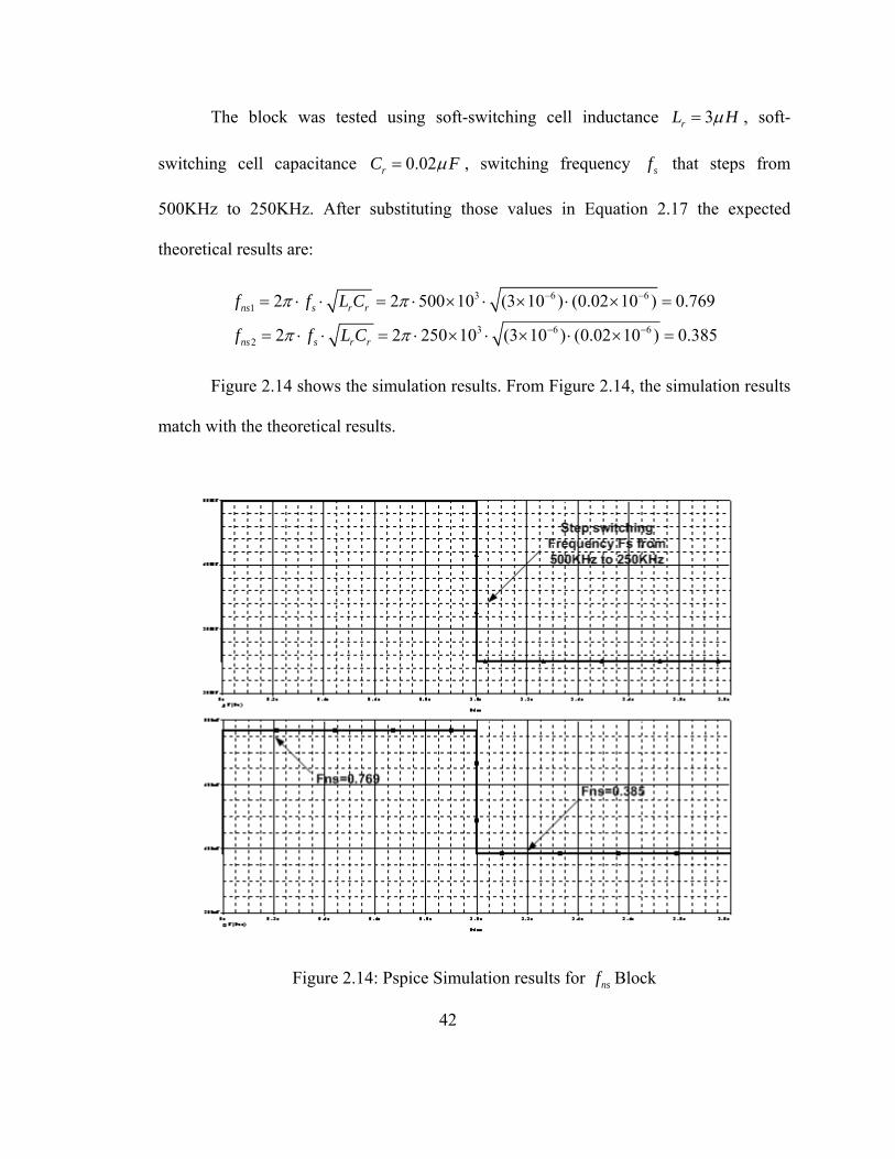
42
HThe block was tested using soft-switching cell inductance 3rL µ= , soft-
switching cell capacitance 0.02rC Fµ= , switching frequency sf that steps from
500KHz to 250KHz. After substituting those values in Equation 2.17 the expected
theoretical results are:
3 6 6
1
3 6 62
2 2 500 10 (3 10 ) (0.02 10 ) 0.769
2 2 250 10 (3 10 ) (0.02 10 ) 0.385
ns s r r
ns s r r
f f L C
f f L C
π π
π π
− −
− −
= ⋅ ⋅ = ⋅ × ⋅ × ⋅ × =
= ⋅ ⋅ = ⋅ × ⋅ × ⋅ × =
Figure 2.14 shows the simulation results. From Figure 2.14, the simulation results
match with the theoretical results.
Figure 2.14: Pspice Simulation results for nsf Block
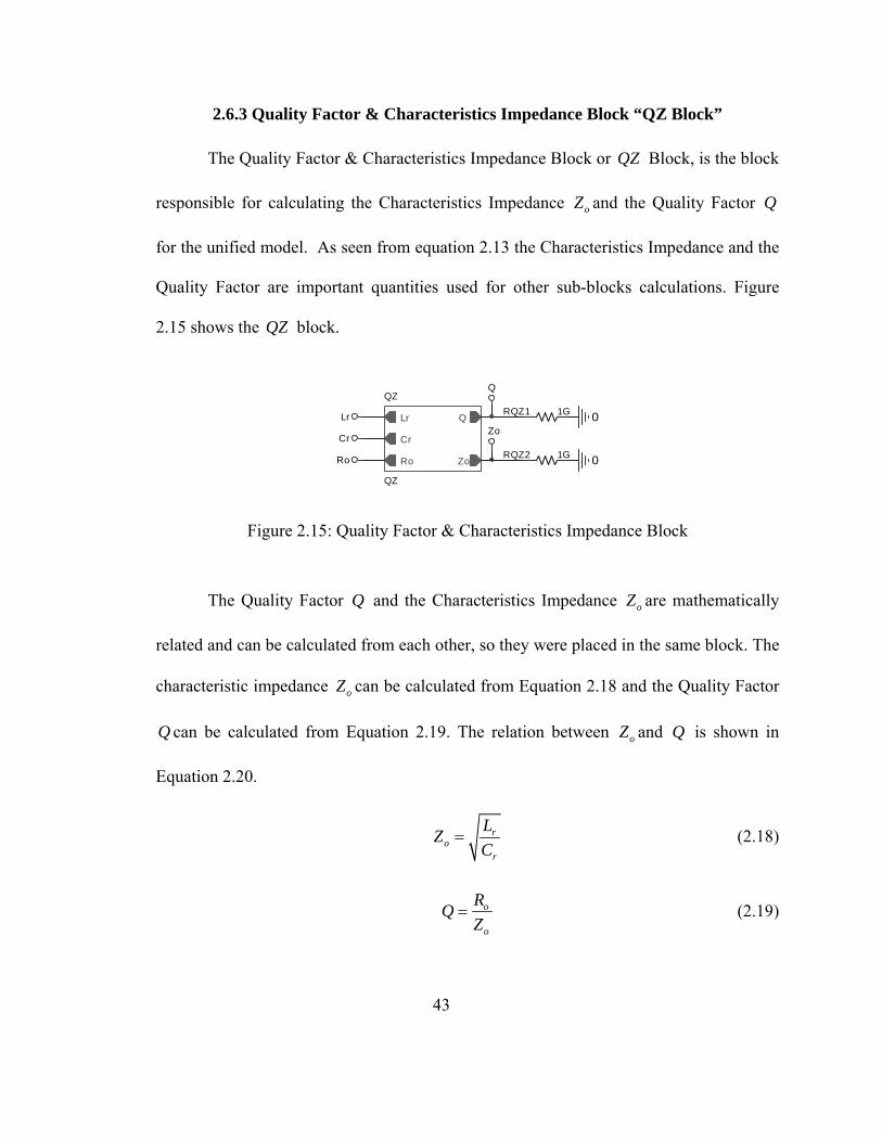
2.6.3 Quality Factor & Characteristics Impedance Block “QZ Block”
The Quality Factor & Characteristics Impedance Block or QZ Block, is the block
responsible for calculating the Characteristics Impedance oZ and the Quality Factor Q
for the unified model. As seen from equation 2.13 the Characteristics Impedance and the
Quality Factor are important quantities used for other sub-blocks calculations. Figure
2.15 shows the block. QZ
Lr 0RQZ1 1GQZ
QZ
Lr
Cr
Q
ZoRoRo
Q
RQZ2 1G 0
CrZo
Figure 2.15: Quality Factor & Characteristics Impedance Block
The Quality Factor Q and the Characteristics Impedance oZ are mathematically
related and can be calculated from each other, so they were placed in the same block. The
characteristic impedance oZ can be calculated from Equation 2.18 and the Quality Factor
can be calculated from Equation 2.19. The relation between Q oZ and is shown in
Equation 2.20.
Q
ro
r
LZC
= (2.18)
o
o
RQZ
= (2.19)
43
o
r
r
RQLC
= (2.20)
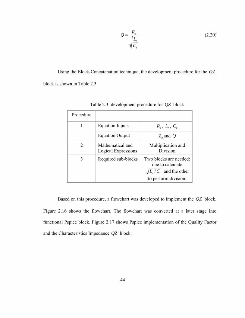
Using the Block-Concatenation technique, the development procedure for the QZ
block is shown in Table 2.3
Table 2.3: development procedure for QZ block
Procedure
Equation Inputs oR , , rL rC1
Equation Output oZ and Q
2 Mathematical and Logical Expressions
Multiplication and Division
3 Required sub-blocks Two blocks are needed: one to calculate /r rL C and the other
to perform division.
Based on this procedure, a flowchart was developed to implement the block.
Figure 2.16 shows the flowchart. The flowchart was converted at a later stage into
functional Pspice block. Figure 2.17 shows Pspice implementation of the Quality Factor
and the Characteristics Impedance block.
QZ
QZ
44
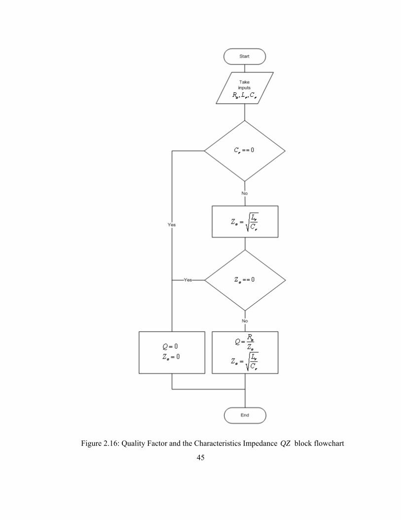
Figure 2.16: Quality Factor and the Characteristics Impedance block flowchart QZ
45
Lr Zo
E_QIF( (V(%IN+)==0),0,(V(%IN-)/V(%IN+)))
EVALUE
OUT+OUT-
IN+IN-
0
Ro
Cr0
QE_Zo
IF( (V(%IN-)==0),0,SQRT( (V(%IN+)/ V(%IN-))))
EVALUE
OUT+OUT-
IN+IN-
Figure 2.17: Pspice implementation of QZ Block
The block was tested using soft-switching cell inductance QZ 3rL Hµ= and
soft-switching cell capacitance 0.02rC Fµ= . Applying equations 2.18 and 2.19
respectively, the expected theoretical results are shown below and Figure 2.18 shows the
simulation results. From Figure 2.18 the simulation results matches with the calculated
theoretical values.
6
6
3.0 10 12.24740.02 10
12 0.9797912.2474
ro
r
o
o
LZC
RQZ
−
−
×= = =
×
= = =
46
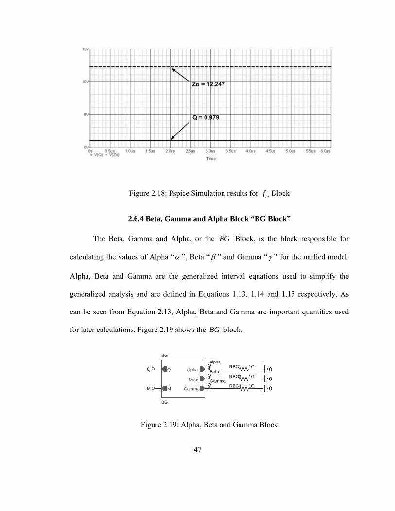
Figure 2.18: Pspice Simulation results for nsf Block
2.6.4 Beta, Gamma and Alpha Block “BG Block”
The Beta, Gamma and Alpha, or the BG Block, is the block responsible for
calculating the values of Alpha “α ”, Beta “β ” and Gamma “γ ” for the unified model.
Alpha, Beta and Gamma are the generalized interval equations used to simplify the
generalized analysis and are defined in Equations 1.13, 1.14 and 1.15 respectively. As
can be seen from Equation 2.13, Alpha, Beta and Gamma are important quantities used
for later calculations. Figure 2.19 shows the BG block.
Beta 0
0RBG3 1G
Q
GammaM
BG
BG
M
Q
Beta
Gamma
alphaRBG1 1G
alpha
RBG2 1G 0
Figure 2.19: Alpha, Beta and Gamma Block
47
From Figure 2.19 the BG block takes two inputs: the Quality factor and the
converter output to input voltage gain
Q
M . From Q and M the BG block calculates the
corresponding values of Alpha, Beta and Gamma. The BG block differs from the
previous two blocks in two main ways: first, it depends on other block calculations to
generate its output. Second, it has a two-way communication with the Main block – The
Main block is the “ ” block defined in Section 2.6.6 -- in other words, the SOL BG block
takes the voltage gain M from the main block and for every iteration, it updates the Main
block with new values of Alpha, Beta and Gamma.
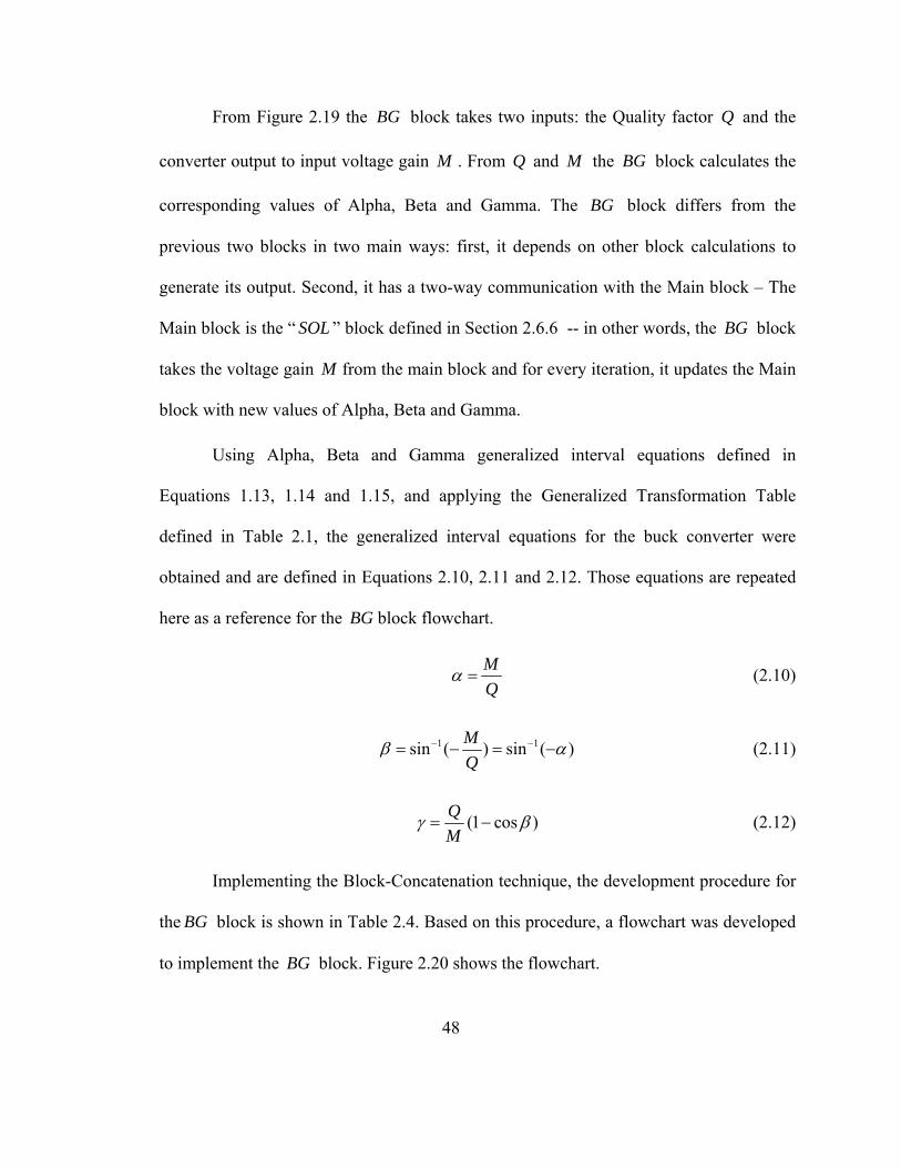
Using Alpha, Beta and Gamma generalized interval equations defined in
Equations 1.13, 1.14 and 1.15, and applying the Generalized Transformation Table
defined in Table 2.1, the generalized interval equations for the buck converter were
obtained and are defined in Equations 2.10, 2.11 and 2.12. Those equations are repeated
here as a reference for the BG block flowchart.
MQ
α = (2.10)
1 1sin ( ) sin ( )MQ
β α− −= − = − (2.11)
(1 cos )QM
γ β= − (2.12)
Implementing the Block-Concatenation technique, the development procedure for
the BG block is shown in Table 2.4. Based on this procedure, a flowchart was developed
to implement the BG block. Figure 2.20 shows the flowchart.
48
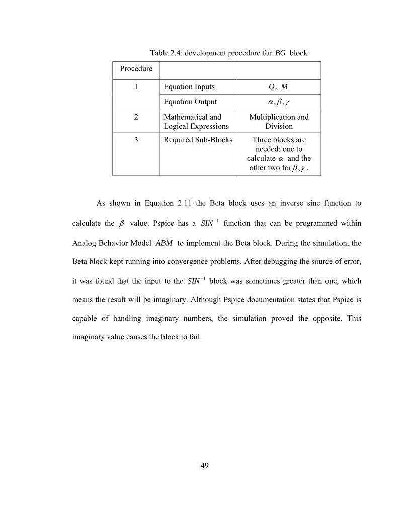
Table 2.4: development procedure for BG block
Procedure
Equation Inputs Q , M 1
Equation Output , ,α β γ
2 Mathematical and Logical Expressions
Multiplication and Division
3 Required Sub-Blocks Three blocks are needed: one to
calculate α and the other two for ,β γ .
As shown in Equation 2.11 the Beta block uses an inverse sine function to
calculate the β value. Pspice has a 1SIN − function that can be programmed within
Analog Behavior Model to implement the Beta block. During the simulation, the
Beta block kept running into convergence problems. After debugging the source of error,
it was found that the input to the
ABM
1SIN − block was sometimes greater than one, which
means the result will be imaginary. Although Pspice documentation states that Pspice is
capable of handling imaginary numbers, the simulation proved the opposite. This
imaginary value causes the block to fail.
49
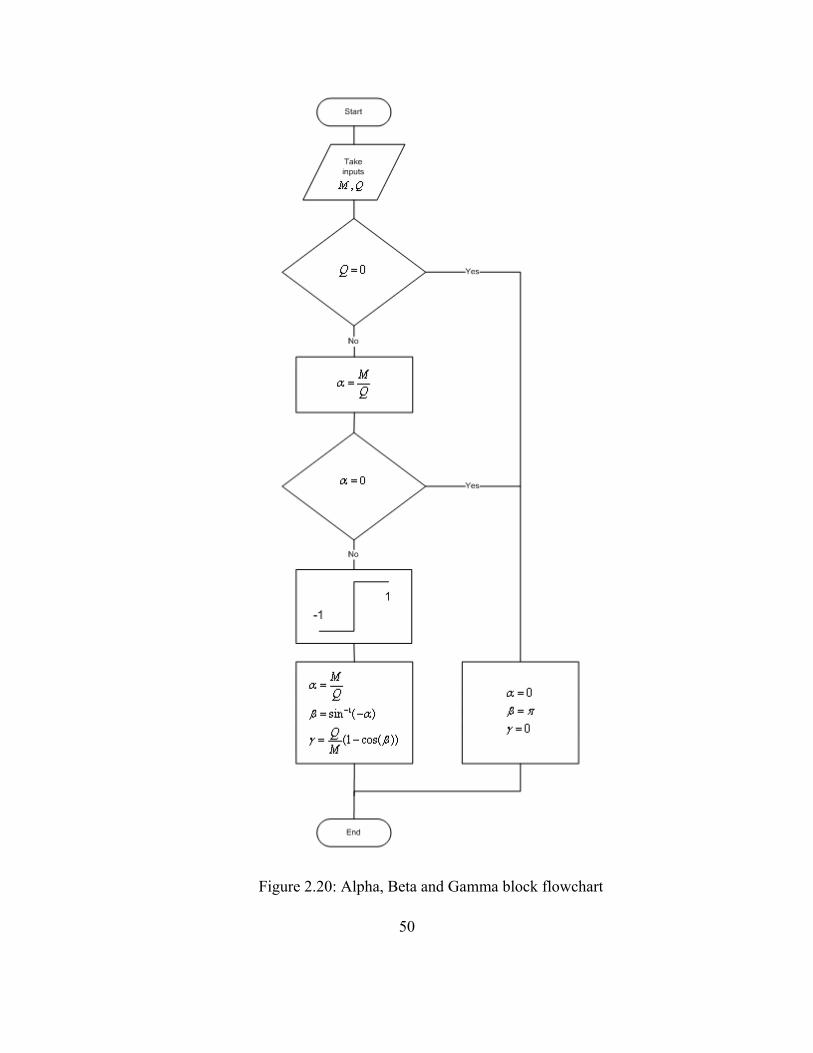
Figure 2.20: Alpha, Beta and Gamma block flowchart
50
One solution to the imaginary value problem is to limit the input to 1SIN −
function to values between -1 and 1 since the 1SIN − function generates real numbers in
this range. The block was tested again with the limiter but it still keeps running into
convergence problems. After testing the block with the limiter function there was a big
question about the functionality of the Pspice 1SIN − function. It was decided to build a
new function with added conditions to avoid convergence problems. 1SIN −
2.6.4.1 Building Inverse Sine function in Pspice
A popular way to rebuild complex non-linear functions like inverse sine or 1SIN −
is by using a series expansion to represent the function around certain point x. Series
expansion is a representation of a particular function as a sum of powers in one of its
variables. The most famous series expansion method is the Taylor series defined in
Equation 2.21. If the series is called the Maclaurin series. The Maclaurin series is a
Taylor series expansion of a function about 0. The general form of the Maclaurin series is
given in Equation 2.22 [21, 22, 23].
0a =
( )
0
( )( ) ( )!
nn
n
f af xn
∞
=
=∑ x a− (2.21)
'' (3) ( )
' 2 3(0) (0) (0)( ) (0) (0)2! 3! !
nnf f ff x f f x x x x
n= + + + + ⋅⋅⋅+ + ⋅⋅⋅ (2.22)
Using the Maclaurin series, the general form of Inverse Sine function or 1SIN − is
given in equation 2.23.
51
( )
1
0
1( )2( )
2 1 !n
n
nSIN x x
n nπ
∞2 1− +
=
Γ +=
+∑ (2.23)
Where:
(2.24)
1
0
1 2
0 0
2
0
( )
( 1)
( 1)
( 1) ( 1).
x t
x t x t
x t
x t e dt
t e x t e dt
x t e dt
x x
∞ − −
∞∞− − − −
∞ − −
Γ =
⎡ ⎤= − + −⎣ ⎦
= −
= − Γ −
∫∫
∫
If x is an integer:
( ) ( )( )( ) ( )( )( )( )( )
( ) 1 1
1 2 2
1 2 3 1
1 !
n n n
n n n
n n n
n
Γ = − Γ −
= − − Γ −
= − − − ⋅⋅
= −
⋅ (2.25)
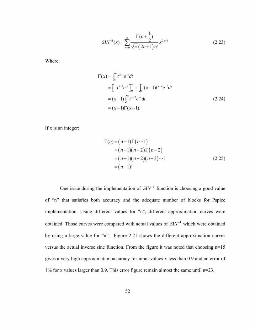
One issue during the implementation of 1SIN − function is choosing a good value
of “n” that satisfies both accuracy and the adequate number of blocks for Pspice
implementation. Using different values for “n”, different approximation curves were
obtained. Those curves were compared with actual values of 1SIN − which were obtained
by using a large value for “n”. Figure 2.21 shows the different approximation curves
versus the actual inverse sine function. From the figure it was noted that choosing n=15
gives a very high approximation accuracy for input values x less than 0.9 and an error of
1% for x values larger than 0.9. This error figure remain almost the same until n=23.
52

Figure 2.21: Maclaurin series approximation versus actual function 1SIN −
Using the Block-Concatenation technique, the development procedure for 1SIN −
block is shown in Table 2.5. Based on this procedure, a flowchart was developed to
implement the block. Figure 2.22 shows the flowchart. 1SIN −
Table 2.5: development procedure for 1SIN − block
Procedure
Equation Input x in the range [-1,1] 1
Equation Output 1( )SIN x−
2 Mathematical and Logical Expressions
Addition,Multiplication and Division
3 Required Sub-Blocks Eight ABM blocks to represent the Maclaurin
series coefficients.
53
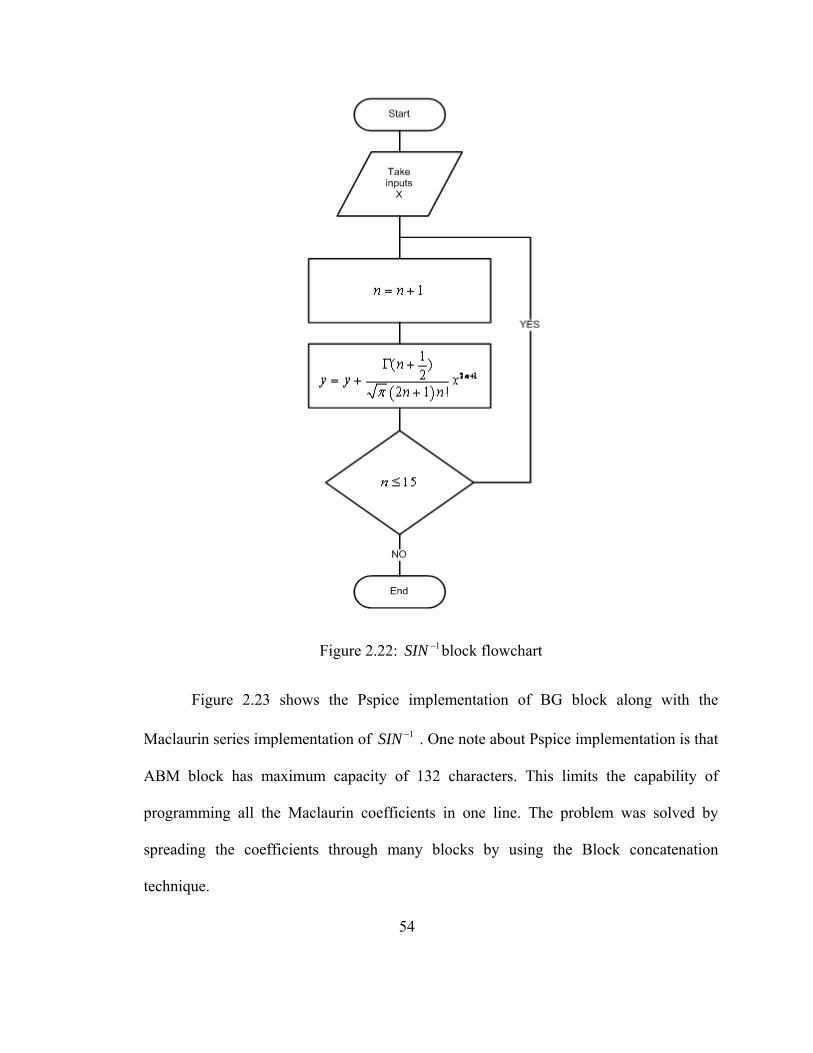
Figure 2.22: 1SIN − block flowchart
Figure 2.23 shows the Pspice implementation of BG block along with the
Maclaurin series implementation of 1SIN − . One note about Pspice implementation is that
ABM block has maximum capacity of 132 characters. This limits the capability of
programming all the Maclaurin coefficients in one line. The problem was solved by
spreading the coefficients through many blocks by using the Block concatenation
technique.
54
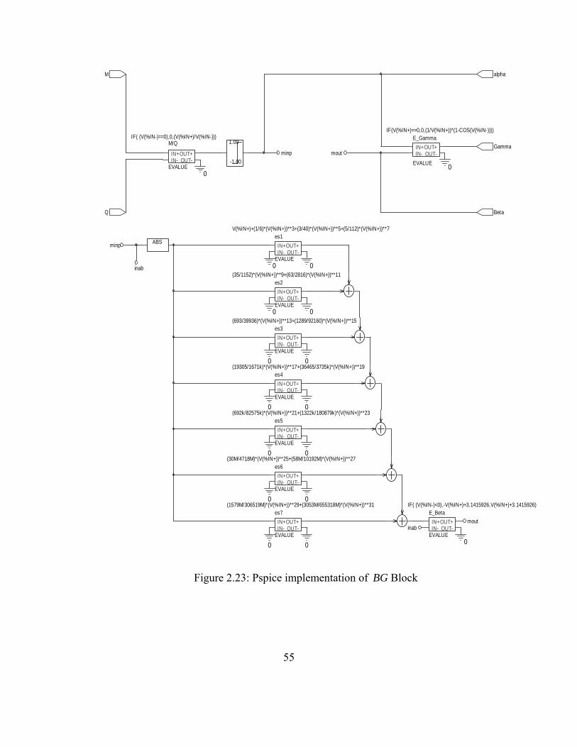
0
0
0
inab
0
0
0
0
inab
minp
E_GammaIF(V(%IN+)==0,0,(1/V(%IN+))*(1-COS(V(%IN-))))
EVALUE
OUT+OUT-
IN+IN-
ABS
0
M
0
0
M/QIF( (V(%IN-)==0),0,(V(%IN+)/V(%IN-)))
EVALUE
OUT+OUT-
IN+IN-
0
0
Gamma
0
Beta
es4(19305/1671k)*(V(%IN+))**17+(36465/3735k)*(V(%IN+))**19
EVALUE
OUT+OUT-
IN+IN-
0
1.00
-1.00
es5(692k/82575k)*(V(%IN+))**21+(1322k/180879k)*(V(%IN+))**23
EVALUE
OUT+OUT-
IN+IN-
es7(1579M/306519M)*(V(%IN+))**29+(3053M/655318M)*(V(%IN+))**31
EVALUE
OUT+OUT-
IN+IN-
0
es3(693/39936)*(V(%IN+))**13+(1289/92160)*(V(%IN+))**15
EVALUE
OUT+OUT-
IN+IN-
E_BetaIF( (V(%IN-)<0),-V(%IN+)+3.1415926,V(%IN+)+3.1415926)
EVALUE
OUT+OUT-
IN+IN-
es2(35/1152)*(V(%IN+))**9+(63/2816)*(V(%IN+))**11
EVALUE
OUT+OUT-
IN+IN-
es6(30M/4718M)*(V(%IN+))**25+(58M/10192M)*(V(%IN+))**27
EVALUE
OUT+OUT-
IN+IN-
mout
es1V(%IN+)+(1/6)*(V(%IN+))**3+(3/40)*(V(%IN+))**5+(5/112)*(V(%IN+))**7
EVALUE
OUT+OUT-
IN+IN-
alpha
mout
Q
0
minp
0
Figure 2.23: Pspice implementation of BG Block
55
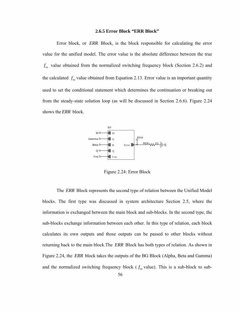
2.6.5 Error Block “ERR Block”
Error block, or Block, is the block responsible for calculating the error
value for the unified model. The error value is the absolute difference between the true
ERR
nsf value obtained from the normalized switching frequency block (Section 2.6.2) and
the calculated nsf value obtained from Equation 2.13. Error value is an important quantity
used to set the conditional statement which determines the continuation or breaking out
from the steady-state solution loop (as will be discussed in Section 2.6.6). Figure 2.24
shows the block. ERR
Fns
Err
M
G
B
Q
Fns
Error
MError
Q
Beta 0
GammaRER 1G
Figure 2.24: Error Block
The Block represents the second type of relation between the Unified Model
blocks. The first type was discussed in system architecture Section 2.5, where the
information is exchanged between the main block and sub-blocks. In the second type, the
sub-blocks exchange information between each other. In this type of relation, each block
calculates its own outputs and those outputs can be passed to other blocks without
returning back to the main block.The Block has both types of relation. As shown in
Figure 2.24, the block takes the outputs of the BG Block (Alpha, Beta and Gamma)
and the normalized switching frequency block (
ERR
ERR
ERR
nsf value). This is a sub-block to sub-56
57
ERRblock relation. In the other type, the block exchanges data with the SOL block
(Section 2.6.6, Error value and steady-state solution). This is sub-block to main-block
relation.
The Block is a direct implementation of the normalized switching frequency
equation developed in Section 2.3. This equation is repeated here as a reference for the
block flowchart.
ERR
ERR
2
2
( sin cos2
nsMf M
Q)
π
γ β γ β γ β
−=
− + − − (2.13)
Using the Block-Concatenation technique, the development procedure for the
block is shown in Table 2.6. Based on this procedure, a flowchart was developed to
implement the block. Figure 2.25 shows the flowchart.
ERR
ERR
Table 2.6: development procedure for block ERR
Procedure
Equation Inputs , , , , nsM Q fβ γ 1
Equation Output Error value
2 Mathematical and Logical Expressions
Addition,Multiplication and Division
3 Required sub-blocks The implementation of Equation (2.13) was divided between five blocks and the sixth block was used to
calculate the absolute error.
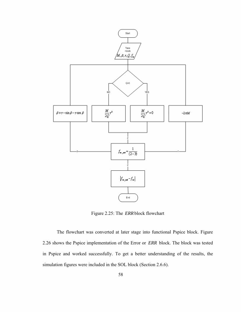
Figure 2.25: The block flowchart ERR
The flowchart was converted at later stage into functional Pspice block. Figure
2.26 shows the Pspice implementation of the Error or block. The block was tested
in Pspice and worked successfully. To get a better understanding of the results, the
simulation figures were included in the SOL block (Section 2.6.6).
ERR
58
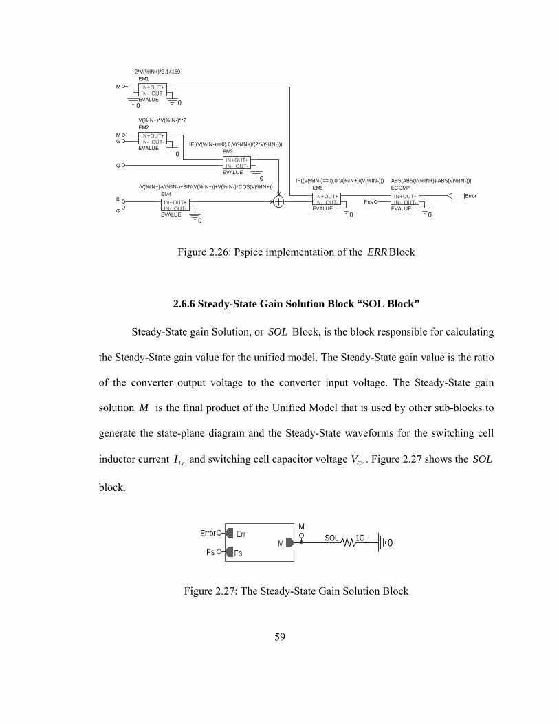
EM2V(%IN+)*V(%IN-)**2
EVALUE
OUT+OUT-
IN+IN-
0
M
0
0
G
Fns
EM1-2*V(%IN+)*3.14159
EVALUE
OUT+OUT-
IN+IN-
0
EM4-V(%IN+)-V(%IN-)+SIN(V(%IN+))+V(%IN-)*COS(V(%IN+))
EVALUE
OUT+OUT-
IN+IN-
EM3IF((V(%IN-)==0),0,V(%IN+)/(2*V(%IN-)))
EVALUE
OUT+OUT-
IN+IN-
B
ECOMPABS(ABS(V(%IN+))-ABS(V(%IN-)))
EVALUE
OUT+OUT-
IN+IN-
Q
ErrorEM5
IF((V(%IN-)==0),0,V(%IN+)/(V(%IN-)))
EVALUE
OUT+OUT-
IN+IN-
0
G
0
M
0
Figure 2.26: Pspice implementation of the Block ERR
2.6.6 Steady-State Gain Solution Block “SOL Block”
Steady-State gain Solution, or Block, is the block responsible for calculating
the Steady-State gain value for the unified model. The Steady-State gain value is the ratio
of the converter output voltage to the converter input voltage. The Steady-State gain
solution
SOL
M is the final product of the Unified Model that is used by other sub-blocks to
generate the state-plane diagram and the Steady-State waveforms for the switching cell
inductor current LrI and switching cell capacitor voltage . Figure 2.27 shows the
block.
CrV SOL
Error Err
FsM
M
Fs
SOL 1G 0
Figure 2.27: The Steady-State Gain Solution Block
59
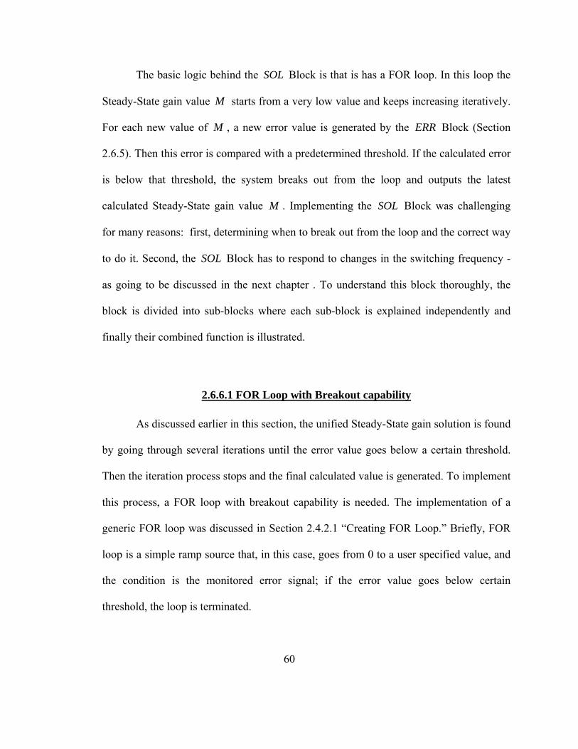
The basic logic behind the Block is that is has a FOR loop. In this loop the
Steady-State gain value
SOL
M starts from a very low value and keeps increasing iteratively.
For each new value of M , a new error value is generated by the ERR Block (Section
2.6.5). Then this error is compared with a predetermined threshold. If the calculated error
is below that threshold, the system breaks out from the loop and outputs the latest
calculated Steady-State gain value M . Implementing the Block was challenging
for many reasons: first, determining when to break out from the loop and the correct way
to do it. Second, the Block has to respond to changes in the switching frequency -
as going to be discussed in the next chapter . To understand this block thoroughly, the
block is divided into sub-blocks where each sub-block is explained independently and
finally their combined function is illustrated.
SOL
SOL
2.6.6.1 FOR Loop with Breakout capability
As discussed earlier in this section, the unified Steady-State gain solution is found
by going through several iterations until the error value goes below a certain threshold.
Then the iteration process stops and the final calculated value is generated. To implement
this process, a FOR loop with breakout capability is needed. The implementation of a
generic FOR loop was discussed in Section 2.4.2.1 “Creating FOR Loop.” Briefly, FOR
loop is a simple ramp source that, in this case, goes from 0 to a user specified value, and
the condition is the monitored error signal; if the error value goes below certain
threshold, the loop is terminated.
60
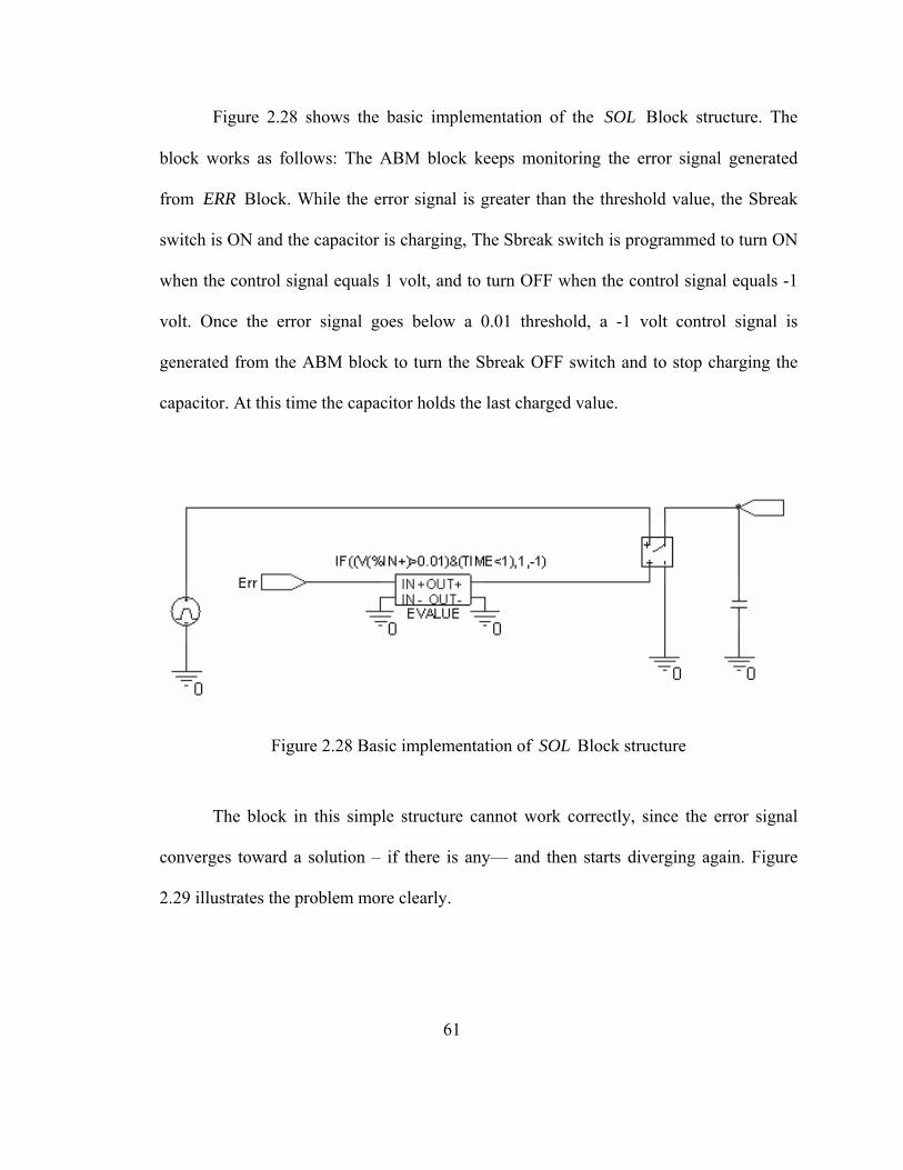
Figure 2.28 shows the basic implementation of the Block structure. The
block works as follows: The ABM block keeps monitoring the error signal generated
from
SOL
ERR Block. While the error signal is greater than the threshold value, the Sbreak
switch is ON and the capacitor is charging, The Sbreak switch is programmed to turn ON
when the control signal equals 1 volt, and to turn OFF when the control signal equals -1
volt. Once the error signal goes below a 0.01 threshold, a -1 volt control signal is
generated from the ABM block to turn the Sbreak OFF switch and to stop charging the
capacitor. At this time the capacitor holds the last charged value.
Figure 2.28 Basic implementation of Block structure SOL
The block in this simple structure cannot work correctly, since the error signal
converges toward a solution – if there is any— and then starts diverging again. Figure
2.29 illustrates the problem more clearly.
61
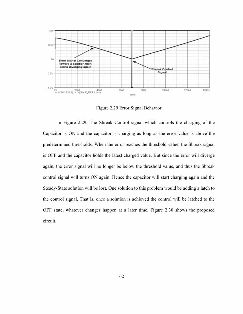
Figure 2.29 Error Signal Behavior
In Figure 2.29, The Sbreak Control signal which controls the charging of the
Capacitor is ON and the capacitor is charging as long as the error value is above the
predetermined thresholds. When the error reaches the threshold value, the Sbreak signal
is OFF and the capacitor holds the latest charged value. But since the error will diverge
again, the error signal will no longer be below the threshold value, and thus the Sbreak
control signal will turns ON again. Hence the capacitor will start charging again and the
Steady-State solution will be lost. One solution to this problem would be adding a latch to
the control signal. That is, once a solution is achieved the control will be latched to the
OFF state, whatever changes happen at a later time. Figure 2.30 shows the proposed
circuit.
62
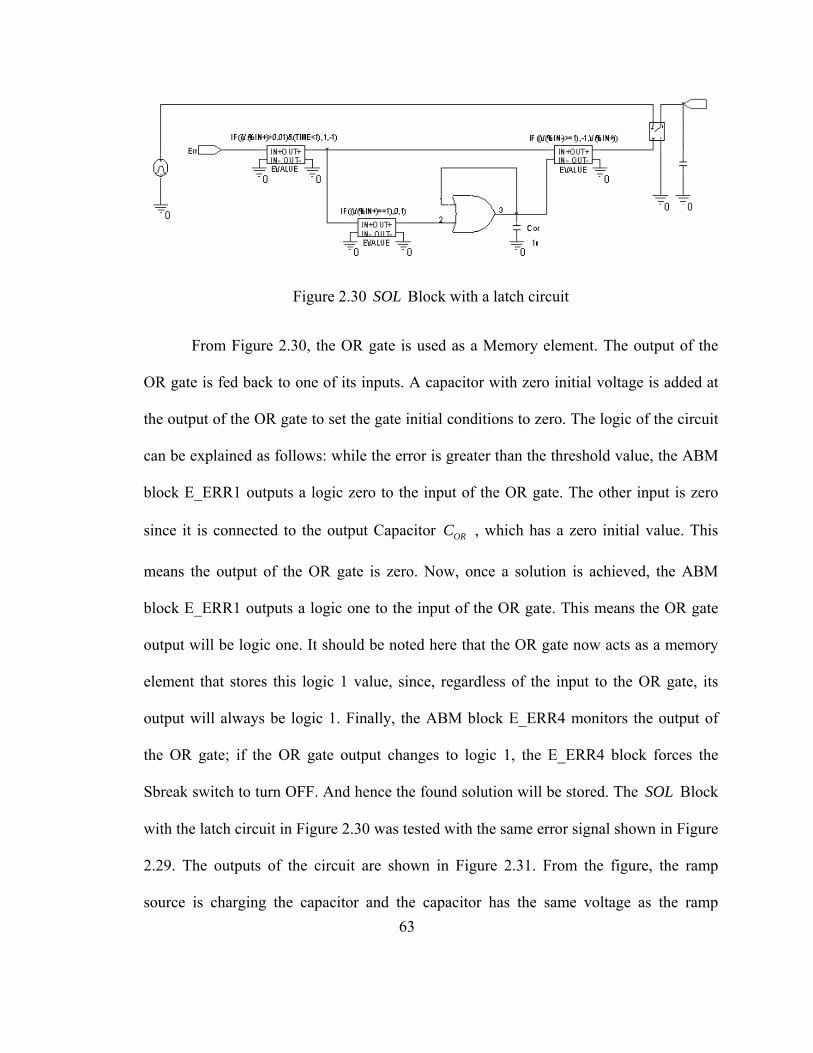
Figure 2.30 Block with a latch circuit SOL
From Figure 2.30, the OR gate is used as a Memory element. The output of the
OR gate is fed back to one of its inputs. A capacitor with zero initial voltage is added at
the output of the OR gate to set the gate initial conditions to zero. The logic of the circuit
can be explained as follows: while the error is greater than the threshold value, the ABM
block E_ERR1 outputs a logic zero to the input of the OR gate. The other input is zero
since it is connected to the output Capacitor , which has a zero initial value. This
means the output of the OR gate is zero. Now, once a solution is achieved, the ABM
block E_ERR1 outputs a logic one to the input of the OR gate. This means the OR gate
output will be logic one. It should be noted here that the OR gate now acts as a memory
element that stores this logic 1 value, since, regardless of the input to the OR gate, its
output will always be logic 1. Finally, the ABM block E_ERR4 monitors the output of
the OR gate; if the OR gate output changes to logic 1, the E_ERR4 block forces the
Sbreak switch to turn OFF. And hence the found solution will be stored. The SOL Block
with the latch circuit in Figure 2.30 was tested with the same error signal shown in Figure
2.29. The outputs of the circuit are shown in Figure 2.31. From the figure, the ramp
source is charging the capacitor and the capacitor has the same voltage as the ramp
ORC
63
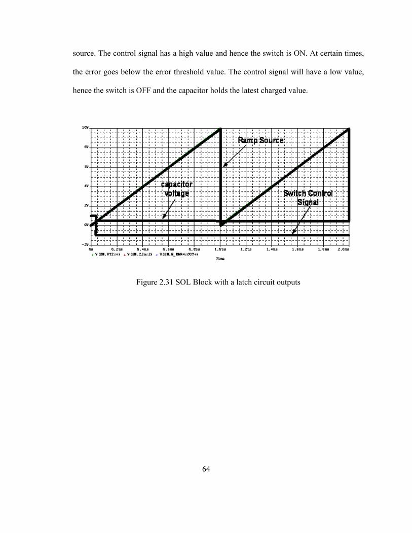
source. The control signal has a high value and hence the switch is ON. At certain times,
the error goes below the error threshold value. The control signal will have a low value,
hence the switch is OFF and the capacitor holds the latest charged value.
Figure 2.31 SOL Block with a latch circuit outputs
64
CHAPTER 3
UNIFIED MODEL APPLICATIONS
3.1 Introduction
The unified steady-state model is a new way to simulate soft-switching cells; the
user connects the simulation model to the desired topology configuration and the Model
calculates the steady-state gain solution for the user. The model also provides the user
with different plots needed for soft-switching cell design. These include the internal
switching cell information such as switching cell inductor current LrI and the switching
cell capacitor voltage , and their corresponding state-plane diagram. The model can
also be used in feedback design applications where the output voltage is regulated by
changing the switching frequency.
CrV
This chapter includes a detailed discussion about how the above applications were
included in the unified model along with their Pspice implementation. Section 3.2
discusses how the unified model generates the switching cell inductor current LrI and the
switching cell capacitor voltage steady-state waveform. Section 3.3 presents the
State-Plane Diagram using the unified model. Section 3.4 shows feedback design using
the unified model and, finally, section 3.5 shows how the model can be used with other
topologies.
CrV
65
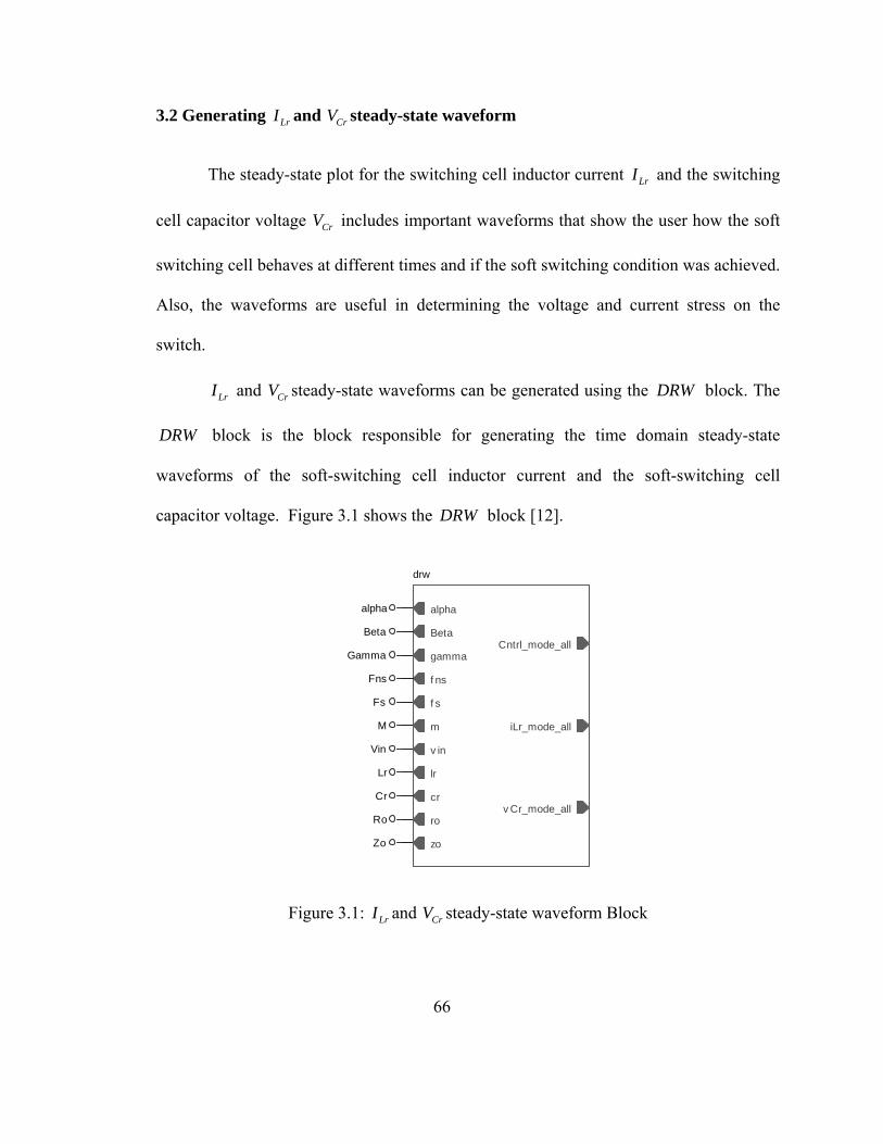
3.2 Generating LrI and steady-state waveform CrV
The steady-state plot for the switching cell inductor current LrI and the switching
cell capacitor voltage includes important waveforms that show the user how the soft
switching cell behaves at different times and if the soft switching condition was achieved.
Also, the waveforms are useful in determining the voltage and current stress on the
switch.
CrV
LrI and steady-state waveforms can be generated using the block. The
block is the block responsible for generating the time domain steady-state
waveforms of the soft-switching cell inductor current and the soft-switching cell
capacitor voltage. Figure 3.1 shows the block [12].
CrV DRW
DRW
DRW
M
Fs
Fns
Beta
Cr
Vin
Lr
Zo
drw
lr
m
zo
f ns
f s
v in
v Cr_mode_all
Cntrl_mode_all
alpha
gamma
iLr_mode_all
Beta
cr
roRo
Gamma
alpha
Figure 3.1: LrI and steady-state waveform Block CrV
66
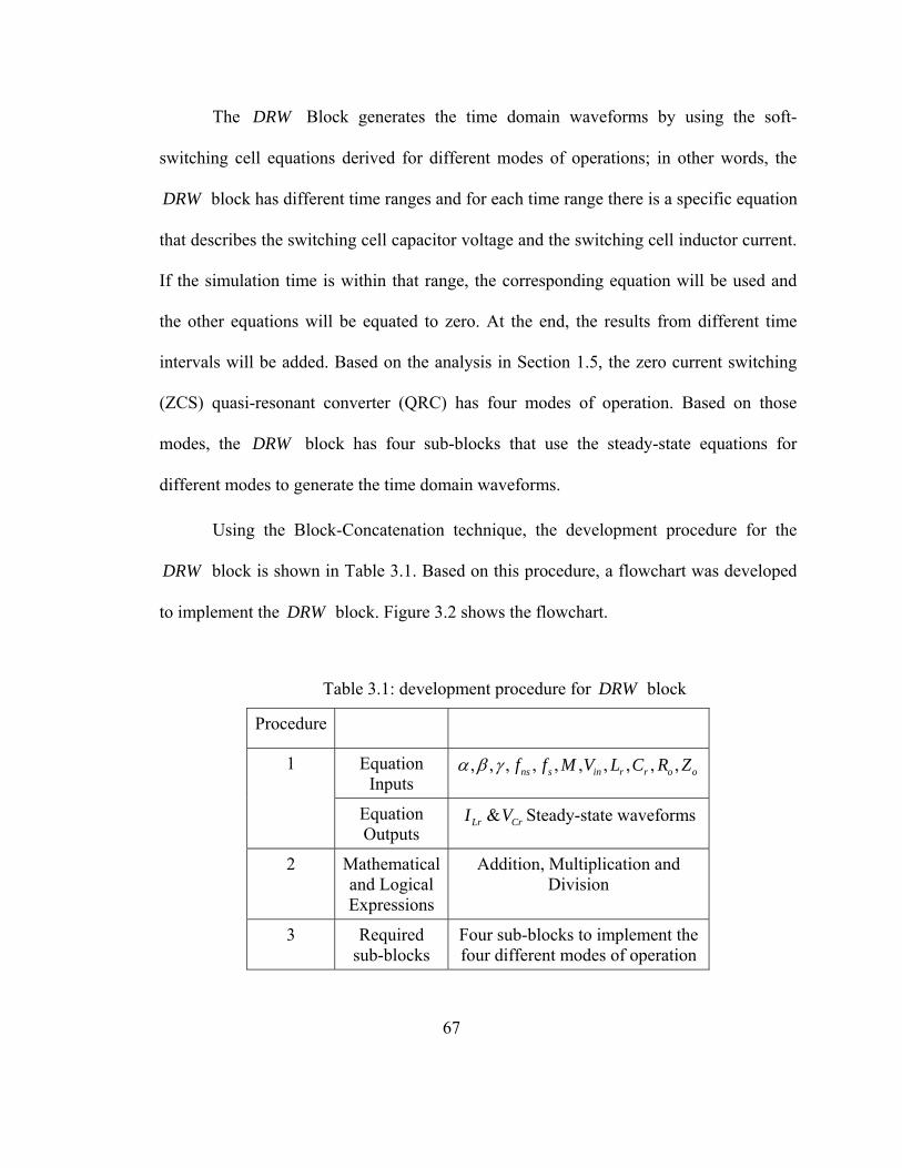
The Block generates the time domain waveforms by using the soft-
switching cell equations derived for different modes of operations; in other words, the
block has different time ranges and for each time range there is a specific equation
that describes the switching cell capacitor voltage and the switching cell inductor current.
If the simulation time is within that range, the corresponding equation will be used and
the other equations will be equated to zero. At the end, the results from different time
intervals will be added. Based on the analysis in Section 1.5, the zero current switching
(ZCS) quasi-resonant converter (QRC) has four modes of operation. Based on those
modes, the block has four sub-blocks that use the steady-state equations for
different modes to generate the time domain waveforms.
DRW
DRW
DRW
Using the Block-Concatenation technique, the development procedure for the
block is shown in Table 3.1. Based on this procedure, a flowchart was developed
to implement the block. Figure 3.2 shows the flowchart.
DRW
DRW
Table 3.1: development procedure for block DRW
Procedure
Equation Inputs
, , , , , , , , , ,ns s in r r o of f M V L C R Zα β γ 1
Equation Outputs
&Lr CrI V Steady-state waveforms
2 Mathematical and Logical Expressions
Addition, Multiplication and Division
3 Required sub-blocks
Four sub-blocks to implement the four different modes of operation
67

Figure 3.2: block flowchart DRW
The following paragraphs summarize the ZCS-QRC four modes of operations and
their corresponding Pspice blocks. The derivation for the equations below was previously
introduced in Chapter 1, Section 1.5.
68
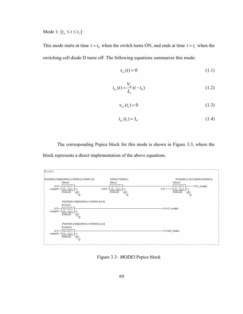
Mode 1: : ][ 1ttto ≤≤
This mode starts at time when the switch turns ON, and ends at time when the
switching cell diode D turns off. The following equations summarize this mode:
0t t= 1t t=
( ) 0crv t = (1.1)
0( ) ( )gLr
r
Vi t t t
L= − (1.2)
1( ) 0Crv t = (1.3)
1( )Lr Fi t I= (1.4)
The corresponding Pspice block for this mode is shown in Figure 3.3, where the
block represents a direct implementation of the above equations.
Eilm12IF(V(%IN-)==0,0,V(%IN+)/V(%IN-))
EVALUE
OUT+OUT-
IN+IN-
v ramp
iLr_mode1
t1v ramp
Cntrl_mode1
00 0
0
0
Econtrol1IF((V(%IN-)>0)&(V(%IN-)<=V(%IN+)),1,0)
EVALUE
OUT+OUT-
IN+IN-
t1
v ramp v in
Ev cm11IF((V(%IN-)>0)&(V(%IN-)<=V(%IN+)),0,0)
EVALUE
OUT+OUT-
IN+IN-
v Cr_mode1
lr
Eilm11V(%IN-)*V(%IN+)
EVALUE
OUT+OUT-
IN+IN-
Mode1
Eilm10IF((V(%IN-)>0)&(V(%IN-)<=V(%IN+)),V(%IN-),0)
EVALUE
OUT+OUT-
IN+IN-
t1
Figure 3.3: 1MODE Pspice block
69
Mode 2: ][ 21 ttt ≤≤ :
This mode starts at time 1t t= when the Diode turns OFF, and ends at time D 2t t=
when the current through drops to zero. The following equations summarize this
mode:
rL
( )0 1( ) 1 cosCr gv t V w t t= − −⎡ ⎤⎣ ⎦ (1.5)
(0 1( ) singLr F
o
Vi t I w t t
Z)= + − (1.6)
2( ) 0Lri t = (1.7)
The corresponding Pspice block for this mode is shown in Figure 3.4, where the
block represents a direct implementation of the above equations.
0
0
0
v in
Ev cm20BIF((V(%IN-)<=V(%IN+)),V(%IN-),0)
EVALUE
OUT+OUT-
IN+IN-
0
zo
EILm24V(%IN+)*V(%IN-)
EVALUE
OUT+OUT-
IN+IN-
Ecntrol2IF(V(%IN+)>0,1,0)
EVALUE
OUT+OUT-
IN+IN-
v ramp
0
EILm23SIN(V(%IN+)*V(%IN-))
EVALUE
OUT+OUT-
IN+IN-
t1
woo
v Cr_mode2
0
t2
0
0
Cntrl_mode2
Ev cm24V(%IN+)*V(%IN-)
EVALUE
OUT+OUT-
IN+IN-
EILm22IF(V(%IN+)>0,(V(%IN+)-V(%IN-)),0)
EVALUE
OUT+OUT-
IN+IN-
EILm25IF(V(%IN-)==0,0,V(%IN+)/V(%IN-))
EVALUE
OUT+OUT-
IN+IN-
0
Ev cm231-COS(V(%IN+)*V(%IN-))
EVALUE
OUT+OUT-
IN+IN-
Iout
t1
0
EILm26
V(%IN+)EVALUE
OUT+OUT-
IN+IN-
v in
Mode2
woo
t1
t2
0
Ev cm22IF(V(%IN+)>0,(V(%IN+)-V(%IN-)),0)
EVALUE
OUT+OUT-
IN+IN-
EILm27IF((V(%IN+)>-1u)&(V(%IN+)<1u),0,V(%IN+)+V(%IN-))
EVALUE
OUT+OUT-
IN+IN-
0 0
Ev cm20AIF((V(%IN-)>=V(%IN+)),V(%IN-),0)
EVALUE
OUT+OUT-
IN+IN-
iLr_mode2
Figure 3.4: 2MODE Pspice block
70

Mode 3: : ][ 32 ttt ≤≤
This mode starts at time when the switch is turned OFF, and ends at time 2t t= S 3tt =
when the capacitor voltage drops to zero causing the diode to turn ON. The following
equations summarize this mode:
D
( ) [2( ) 1 cosFCr g
r
Iv t t t VC
]β= − − + − (1.8)
( ) 0Lri t = (1.9)
3( ) 0Crv t = (1.10)
The corresponding Pspice block for this mode is shown in Figure 3.5, where the
block represents a direct implementation of the above equations.
Ecntrol3IF(V(%IN+)>0,0,0)
EVALUE
OUT+OUT-
IN+IN-
cr
00 0
Ev cm36IF(V(%IN+) < 0.0 ,V(%IN+)+V(%IN-),0)
EVALUE
OUT+OUT-
IN+IN-
0
Ev cm32IF(V(%IN+)>0,(V(%IN+)-V(%IN-)),0)
EVALUE
OUT+OUT-
IN+IN-
Ev cm34IF(V(%IN-)==0,0,V(%IN+)/V(%IN-))
EVALUE
OUT+OUT-
IN+IN-
0
0
0Iout
Ev cm35V(%IN+)*(1-COS(V(%IN-)))
EVALUE
OUT+OUT-
IN+IN-
v Cr_mode3t2
0
Mode3
EILm31IF(V(%IN+)>0,0,0)
EVALUE
OUT+OUT-
IN+IN-
v in
0
Ev cm30AIF((V(%IN-)>=V(%IN+)),V(%IN-),0)
EVALUE
OUT+OUT-
IN+IN-
Beta
Ev cm33-(V(%IN+)*V(%IN-))
EVALUE
OUT+OUT-
IN+IN-
0
0
t2
Cntrl_mode3
Ev cm30BIF((V(%IN-)<=V(%IN+)),V(%IN-),0)
EVALUE
OUT+OUT-
IN+IN-v ramp
t3
iLr_mode3
Figure 3.5: 3MODE Pspice block
71
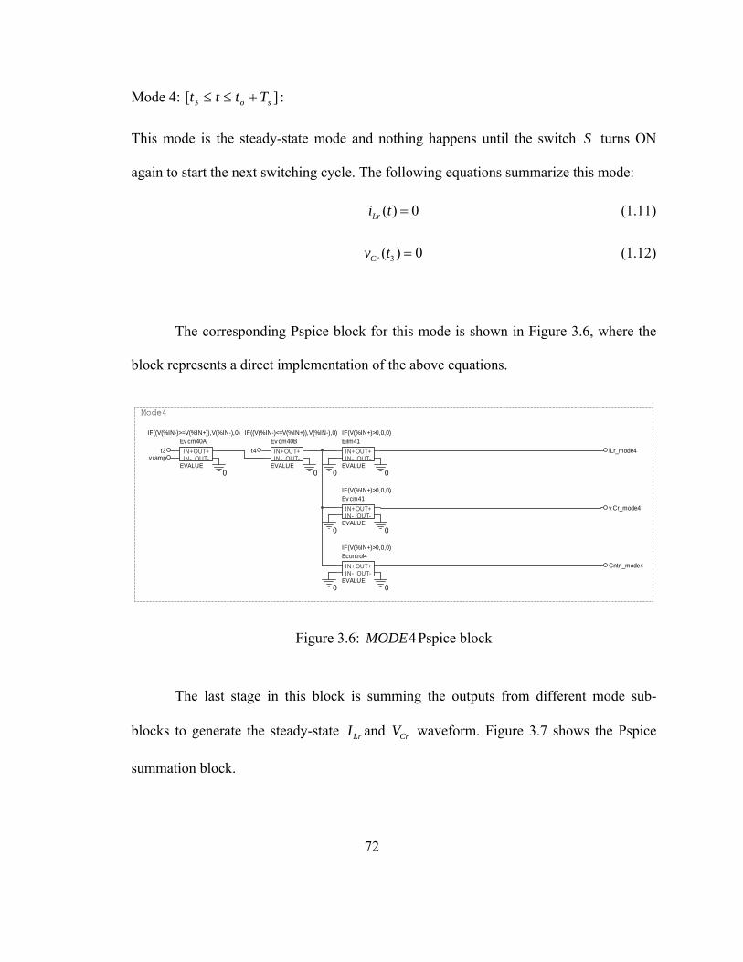
Mode 4: ][ 3 so Tttt +≤≤ :
This mode is the steady-state mode and nothing happens until the switch turns ON
again to start the next switching cycle. The following equations summarize this mode:
S
( ) 0Lri t = (1.11)
3( ) 0Crv t = (1.12)
The corresponding Pspice block for this mode is shown in Figure 3.6, where the
block represents a direct implementation of the above equations.
t3
0
Mode4
t4 iLr_mode4
0
0
0
Ev cm41IF(V(%IN+)>0,0,0)
EVALUE
OUT+OUT-
IN+IN-
Ev cm40AIF((V(%IN-)>=V(%IN+)),V(%IN-),0)
EVALUE
OUT+OUT-
IN+IN-v ramp
Cntrl_mode4
0
Eilm41IF(V(%IN+)>0,0,0)
EVALUE
OUT+OUT-
IN+IN-
0
Ev cm40BIF((V(%IN-)<=V(%IN+)),V(%IN-),0)
EVALUE
OUT+OUT-
IN+IN-
0
Econtrol4IF(V(%IN+)>0,0,0)
EVALUE
OUT+OUT-
IN+IN-
v Cr_mode4
0
Figure 3.6: 4MODE Pspice block
The last stage in this block is summing the outputs from different mode sub-
blocks to generate the steady-state LrI and waveform. Figure 3.7 shows the Pspice
summation block.
CrV
72
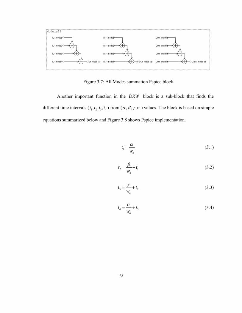
v Cr_mode_all Cntrl_mode4
v Cr_mode3
Cntrl_mode1iLr_mode1
Cntrl_mode2
Mode_all
v Cr_mode1
v Cr_mode2
iLr_mode4 iLr_mode_all
iLr_mode3 Cntrl_mode3
iLr_mode2
Cntrl_mode_allv Cr_mode4
Figure 3.7: All Modes summation Pspice block
Another important function in the block is a sub-block that finds the
different time intervals ( ) from (
DRW
1 2 3 4, , ,t t t t , , ,α β γ σ ) values. The block is based on simple
equations summarized below and Figure 3.8 shows Pspice implementation.
1o
twα
= (3.1)
2o
tw 1tβ
= + (3.2)
3o
tw 2tγ
= + (3.3)
4o
tw 3tσ
= + (3.4)
73
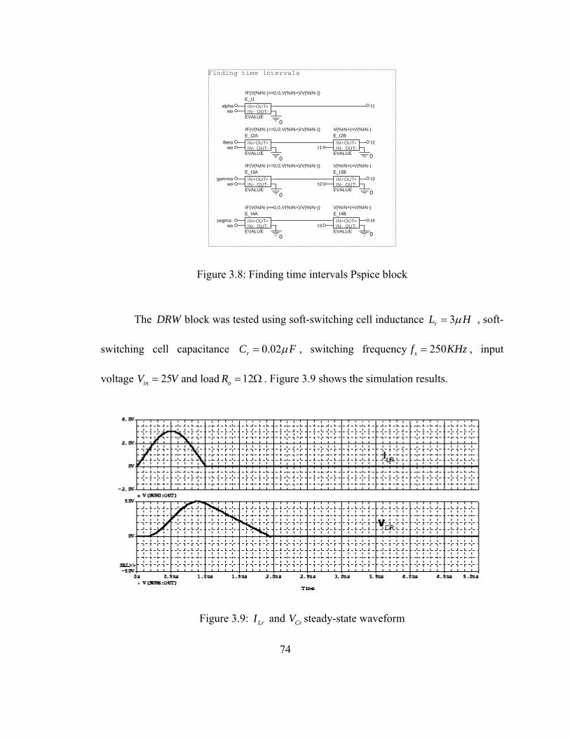
0 0
0
0
t1
t3
E_t1IF(V(%IN-)==0,0,V(%IN+)/V(%IN-))
EVALUE
OUT+OUT-
IN+IN-
t3
E_t4AIF(V(%IN-)==0,0,V(%IN+)/V(%IN-))
EVALUE
OUT+OUT-
IN+IN-
alpha
0
t1
t2
E_t2AIF(V(%IN-)==0,0,V(%IN+)/V(%IN-))
EVALUE
OUT+OUT-
IN+IN-
wo
t2
0
E_t4BV(%IN+)+V(%IN-)
EVALUE
OUT+OUT-
IN+IN-
E_t2BV(%IN+)+V(%IN-)
EVALUE
OUT+OUT-
IN+IN-
segma
wo
t4
wo
Finding time intervals
E_t3BV(%IN+)+V(%IN-)
EVALUE
OUT+OUT-
IN+IN-
E_t3AIF(V(%IN-)==0,0,V(%IN+)/V(%IN-))
EVALUE
OUT+OUT-
IN+IN-
gammawo
Beta
0
Figure 3.8: Finding time intervals Pspice block
The block was tested using soft-switching cell inductance DRW 3rL Hµ= , soft-
switching cell capacitance 0.02rC Fµ= , switching frequency 250sf KHz= , input
voltage and load25inV = V 12oR = Ω . Figure 3.9 shows the simulation results.
Figure 3.9: LrI and steady-state waveform CrV
74
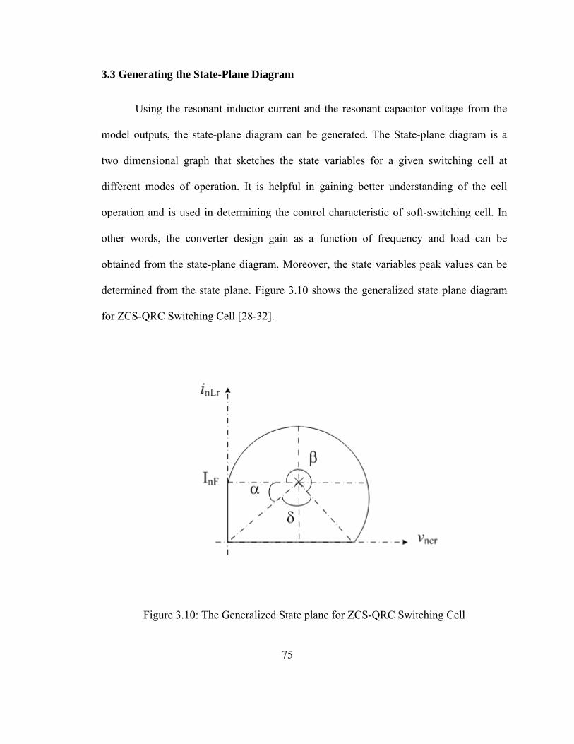
3.3 Generating the State-Plane Diagram
Using the resonant inductor current and the resonant capacitor voltage from the
model outputs, the state-plane diagram can be generated. The State-plane diagram is a
two dimensional graph that sketches the state variables for a given switching cell at
different modes of operation. It is helpful in gaining better understanding of the cell
operation and is used in determining the control characteristic of soft-switching cell. In
other words, the converter design gain as a function of frequency and load can be
obtained from the state-plane diagram. Moreover, the state variables peak values can be
determined from the state plane. Figure 3.10 shows the generalized state plane diagram
for ZCS-QRC Switching Cell [28-32].
Figure 3.10: The Generalized State plane for ZCS-QRC Switching Cell
75
The Generalized state plane diagram analysis can be used to derive other
characteristic equations for the generalized switching cell such as the generalized peak
resonant capacitor voltage , the generalized peak resonant inductor current ,ncr PV ,nLr PI ,
the generalized peak switch current and voltage ,n sw pI − & ,n sw pV − and generalized average
switch current and voltage & . The equations for the above parameters are
summarized below [3, 30, 31]:
,n sw aveV − ,n sw aveI −
ngPncr VV 2, = (3.5)
,ng
nLr P nF
QVI I
M= + (3.6)
ngnFpswn VII +=−, (3.7)
ngpswn VV =−, (3.8)
nbnFnDnFaveswn IIIII −=−=−, (3.9)
nFngaveswn VVV −=−, (3.10)
The state plane figure can be generated in the unified model by using LrI and
steady-state waveform block “ Block.” The Block generates the steady-state
waveforms for the soft-switching cell inductor current
CrV
DRW DRW
LrI and the soft-switching cell
capacitor voltage . The state plane diagram can be generated by plotting versus CrV CrV
LrI in Pspice. 76
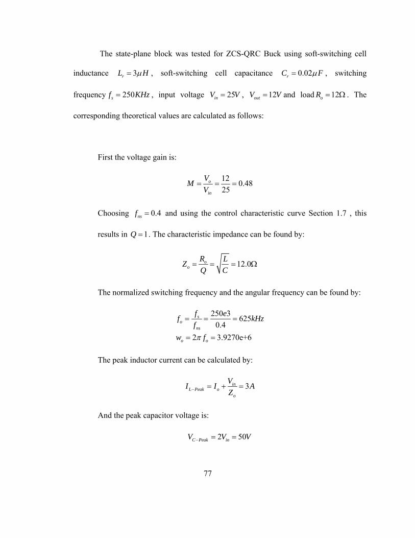
77
H
The state-plane block was tested for ZCS-QRC Buck using soft-switching cell
inductance 3rL µ= , soft-switching cell capacitance 0.02rC Fµ= , switching
frequency 250sf KHz= , input voltage 25inV V= , 12outV V= and load . The
corresponding theoretical values are calculated as follows:
12oR = Ω
First the voltage gain is:
12 0.4825
o
in
VMV
= = =
Choosing and using the control characteristic curve Section 1.7 , this
results in . The characteristic impedance can be found by:
0.4nsf =
1Q =
12.0oo
R LZQ C
= = = Ω
The normalized switching frequency and the angular frequency can be found by:
250 3 625
0.42 3.9270e+6
so
ns
o o
f ef kHzf
w fπ
= = =
= =
The peak inductor current can be calculated by:
3inL Peak o
o
VI I AZ− = + =
And the peak capacitor voltage is:
2 50C Peak inV V− V= =
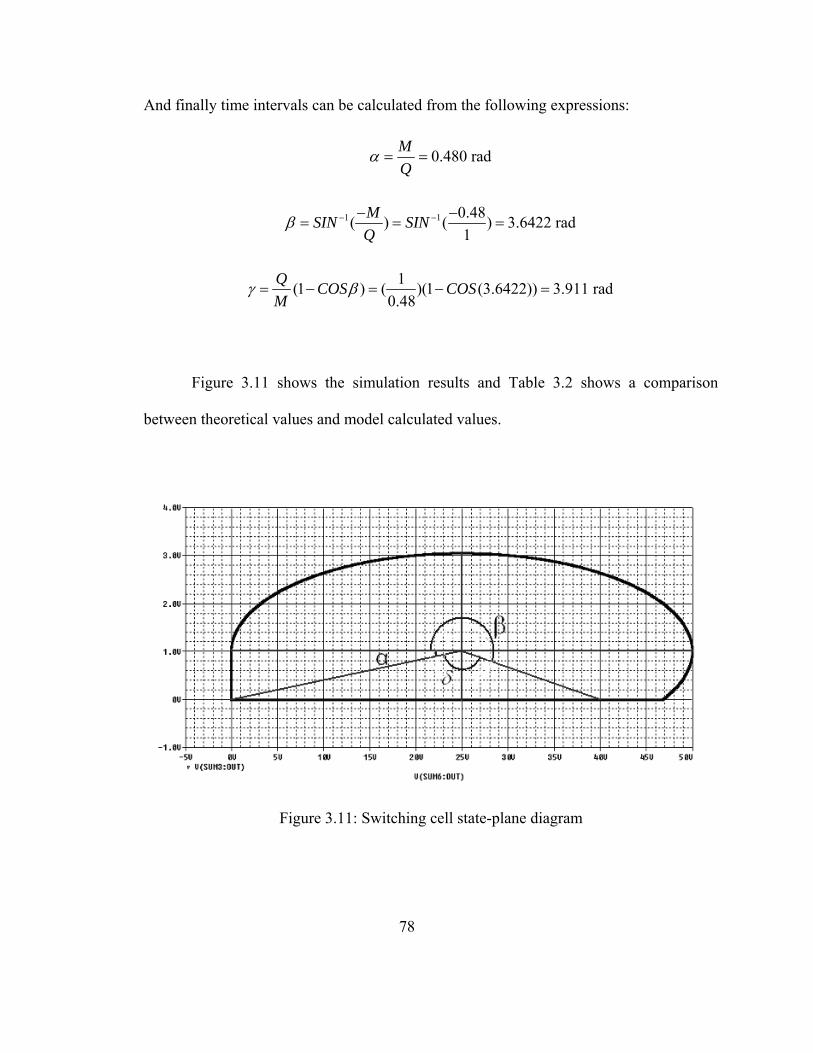
And finally time intervals can be calculated from the following expressions:
0.480 radMQ
α = =
1 1 0.48( ) ( ) 3.6422 rad1
MSIN SINQ
β − −− −= = =
1(1 ) ( )(1 (3.6422)) 3.911 rad0.48
Q COS COSM
γ β= − = − =
Figure 3.11 shows the simulation results and Table 3.2 shows a comparison
between theoretical values and model calculated values.
Figure 3.11: Switching cell state-plane diagram
78

Table 3.2: Comparison between theoretical values and Model calculated values.
Parameter Theoretical Value Model Value
α 0.480 rad 0.4898 rad
β 3.6422 rad 3.6535 rad
γ 3.911 rad 3.8207 rad
σ 7.6748 rad 7.744 rad
L PeakI − 3 A 3A
C PeakV − 50 V 50 V
3.4 Feedback Design
The unified steady-state model can be used for feedback design in applications
where the output voltage is regulated by changing the switching frequency sf .Figure 3.12
shows a general block diagram of the closed loop system using Pspice unified model. It
should be noted here that feedback design using the unified model is still in progress and
this section presents only the work done so far. Future publications will contain a detailed
complete discussion about feedback design using the unified model.
Figure 3.12: Closed loop using the unified general model
79

The closed loop starts by sensing the output voltage from the unified model; this
voltage is then compared with the desired reference voltage. The error signal generated is
fed to a voltage-controlled oscillator which in turn generates a frequency value that
depends on the error signal. This new frequency will regulate the output voltage.
The unified model in its current structure cannot regulate the output voltage since
the model cannot detect frequency changes. The next sections describe the necessary
changes in SOL block to detect frequency changes and to find new solutions if there is a
frequency change.
3.4.1 Detecting changes in switching frequency
For Quasi resonant cells the output voltage is regulated by changing the switching
frequency. The unified model needs to detect frequency changes to update its different
parameters and its final steady-state gain solution. There are two difficulties in building
this functionality: first, building the circuit that detects changes in the input variable;
second, the unified model at this stage needs 1u second to find a steady-state solution.
The detecting circuit should not interrupt the unified model blocks within the 1u second
period and at the same time it should latch a signal to the solution block showing that a
change has occurred in the switching frequency so that a new solution cycle starts.
Frequency change detection circuit was built using the sample and hold concept.
The switching frequency sf is processed by two sample and hold circuits. A sample and
hold circuit is simply a switch and a capacitorthe switch turns ON and the capacitor
starts charging to the input voltage value, and then the switch turns OFF and the capacitor
80
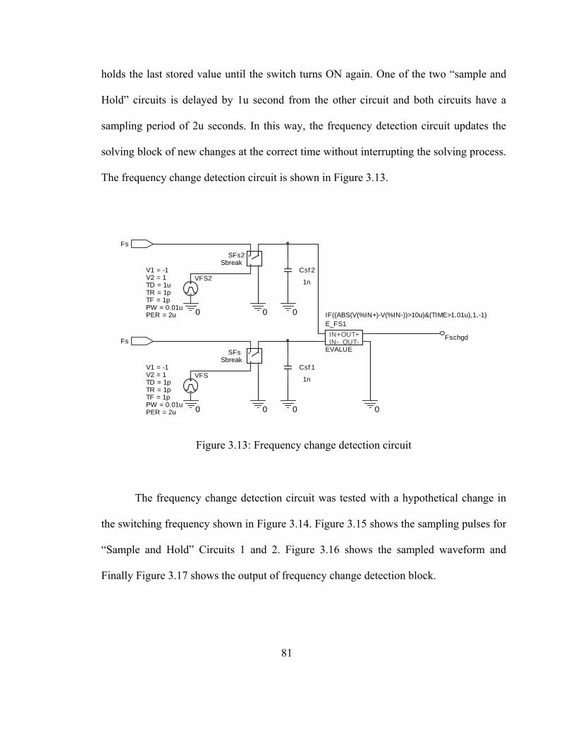
holds the last stored value until the switch turns ON again. One of the two “sample and
Hold” circuits is delayed by 1u second from the other circuit and both circuits have a
sampling period of 2u seconds. In this way, the frequency detection circuit updates the
solving block of new changes at the correct time without interrupting the solving process.
The frequency change detection circuit is shown in Figure 3.13.
0
0
Csf 1
1n
Csf 2
1n
0
VFSTD = 1p
TF = 1pPW = 0.01uPER = 2u
V1 = -1
TR = 1p
V2 = 1
0
Fs
E_FS1IF((ABS(V(%IN+)-V(%IN-))>10u)&(TIME>1.01u),1,-1)
EVALUE
OUT+OUT-
IN+IN-
Fs+ -
+ -Sbreak
SFs2
0
+ -
+ -
SbreakSFs
Fschgd
00
VFS2TD = 1u
TF = 1pPW = 0.01uPER = 2u
V1 = -1
TR = 1p
V2 = 1
Figure 3.13: Frequency change detection circuit
The frequency change detection circuit was tested with a hypothetical change in
the switching frequency shown in Figure 3.14. Figure 3.15 shows the sampling pulses for
“Sample and Hold” Circuits 1 and 2. Figure 3.16 shows the sampled waveform and
Finally Figure 3.17 shows the output of frequency change detection block.
81
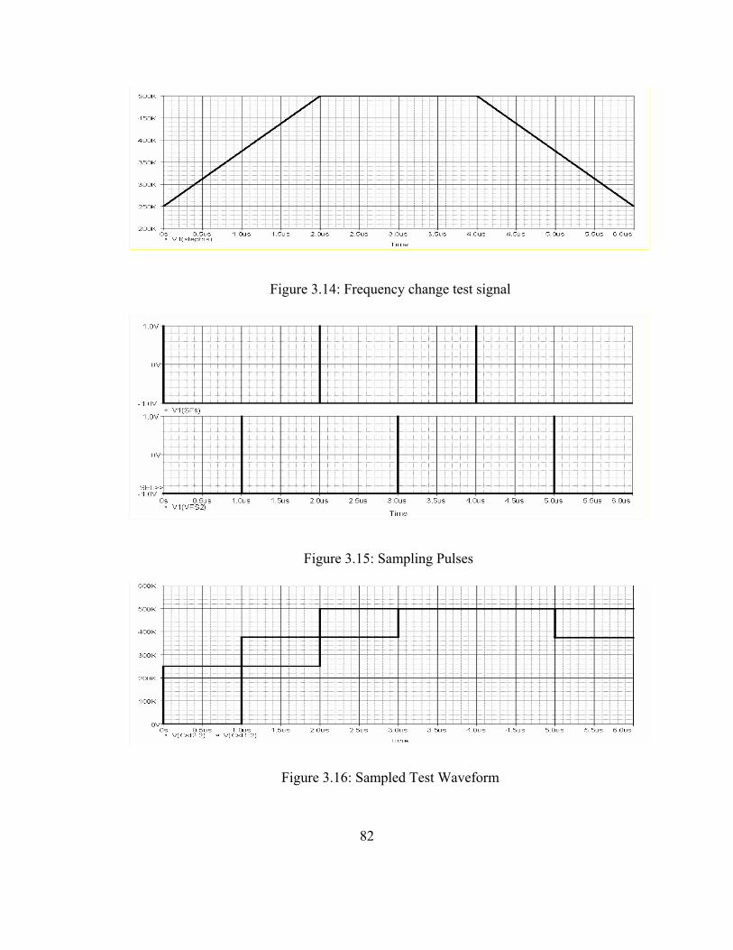
Figure 3.14: Frequency change test signal
Figure 3.15: Sampling Pulses
Figure 3.16: Sampled Test Waveform
82
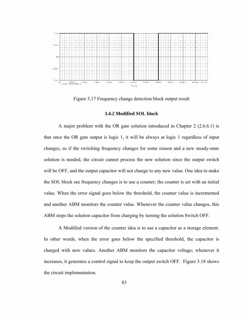
Figure 3.17 Frequency change detection block output result
3.4.2 Modified SOL block
A major problem with the OR gate solution introduced in Chapter 2 (2.6.6.1) is
that once the OR gate output is logic 1, it will be always at logic 1 regardless of input
changes, so if the switching frequency changes for some reason and a new steady-state
solution is needed, the circuit cannot process the new solution since the output switch
will be OFF, and the output capacitor will not change to any new value. One idea to make
the SOL block see frequency changes is to use a counter; the counter is set with an initial
value. When the error signal goes below the threshold, the counter value is incremented
and another ABM monitors the counter value. Whenever the counter value changes, this
ABM stops the solution capacitor from charging by turning the solution Switch OFF.
A Modified version of the counter idea is to use a capacitor as a storage element.
In other words, when the error goes below the specified threshold, the capacitor is
charged with new values. Another ABM monitors the capacitor voltage; whenever it
increases, it generates a control signal to keep the output switch OFF. Figure 3.18 shows
the circuit implementation.
83
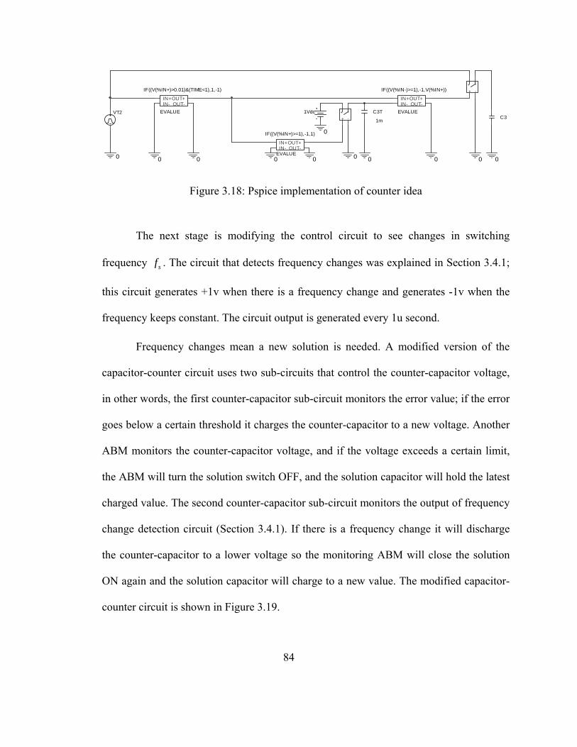
00
C3
0
IF((V(%IN-)>=1),-1,V(%IN+))
EVALUE
OUT+OUT-
IN+IN-
0
IF((V(%IN+)>0.01)&(TIME<1),1,-1)
EVALUE
OUT+OUT-
IN+IN-
+ -
+ -
0
00 0
C3T
1m
+ -
+ -
1Vdc
00
VT2
0
IF((V(%IN+)>=1),-1,1)
EVALUE
OUT+OUT-
IN+IN-
Figure 3.18: Pspice implementation of counter idea
The next stage is modifying the control circuit to see changes in switching
frequency sf . The circuit that detects frequency changes was explained in Section 3.4.1;
this circuit generates +1v when there is a frequency change and generates -1v when the
frequency keeps constant. The circuit output is generated every 1u second.
Frequency changes mean a new solution is needed. A modified version of the
capacitor-counter circuit uses two sub-circuits that control the counter-capacitor voltage,
in other words, the first counter-capacitor sub-circuit monitors the error value; if the error
goes below a certain threshold it charges the counter-capacitor to a new voltage. Another
ABM monitors the counter-capacitor voltage, and if the voltage exceeds a certain limit,
the ABM will turn the solution switch OFF, and the solution capacitor will hold the latest
charged value. The second counter-capacitor sub-circuit monitors the output of frequency
change detection circuit (Section 3.4.1). If there is a frequency change it will discharge
the counter-capacitor to a lower voltage so the monitoring ABM will close the solution
ON again and the solution capacitor will charge to a new value. The modified capacitor-
counter circuit is shown in Figure 3.19.
84
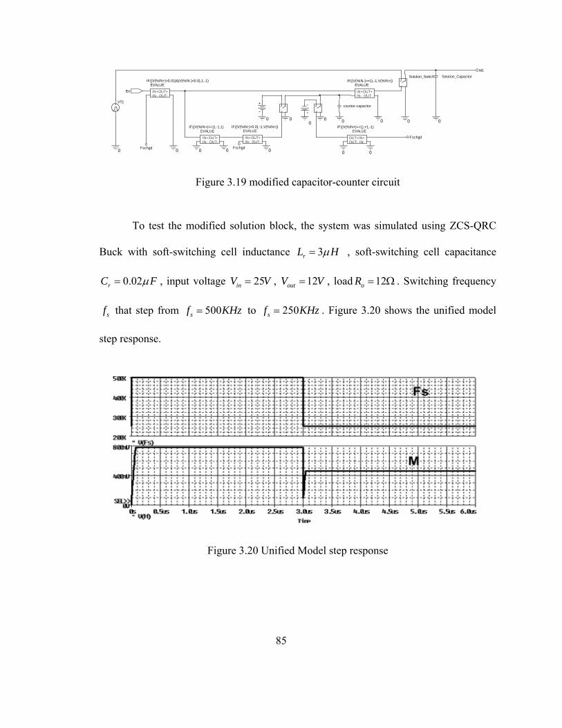
0
0 Fschgd
0
Solution_Capacitor
VT2
Fschgd
0
0
+ -+ -
IF((V(%IN-)>0.0),-1,V(%IN+))EVALUE
OUT+OUT-
IN+IN-
0
0
IF((V(%IN+)>0.01)&(V(%IN-)<0.0),1,-1)EVALUE
OUT+OUT-
IN+IN-
Err
+ -+ -
Solution_Switch
0 0
+ -+ -
0
IF((V(%IN-)>=1),-1,V(%IN+))EVALUE
OUT+OUT-
IN+IN-
00 0Fschgd
IF((V(%IN+)>=1),-1,1)EVALUE
OUT+OUT-
IN+IN-
M1
0IF((V(%IN+)>=1),+1,-1)
EVALUE
OUT+OUT-
IN+IN-
counter-capacitor
0
Figure 3.19 modified capacitor-counter circuit
To test the modified solution block, the system was simulated using ZCS-QRC
Buck with soft-switching cell inductance 3rL Hµ= , soft-switching cell capacitance
0.02rC Fµ= , input voltage 25inV V= , 12outV V= , load 12oR = Ω . Switching frequency
sf that step from 500sf KHz= to 250sf KHz= . Figure 3.20 shows the unified model
step response.
Figure 3.20 Unified Model step response
85

3.5 Unified Model for common DC-DC converters families
The unified steady-state simulation model can be used with the most common
DC-DC converter family, namely, buck, boost, buck-boost, cuck, zeta and sepic. The user
chooses the soft-switching cell type and connects the Unified model in the desired
topology configuration. In order for the unified model to generate the correct steady-state
values, the model needs to know the topology it is connected to. In previous chapters, the
unified model was used in one topology type, the buck converter. This section
summarizes how the unified model can be used with other DC-DC converters families.
3.5.1 Unified Model for Boost converter family
For the Boost topology and based on the discussion on chapter 1, the ZCS-QRC
will have the same switching waveforms and the same modes of operation regardless of
the cell orientation [2,3]. Using the generalized steady-state analysis in section 1.6, the
generalized interval equations are:
1 0( ) nFo
ng
MIt tQV
α ω= − = (1.13)
12 1( ) sin ( nF
ong
)MIt tQV
β ω −= − = − (1.14)
3 2( ) (1 cosngo
nF
QVt t
MI)γ ω= − = − β (1.15)
0 32(( ) )o s
ns
t T tfπδ ω= + − = − −α β γ− (1.16)
86

By substituting for the generalized parameters ( and ) from Table 1.1 the
corresponding intervals for the Boost topology are:
ngV nFI
1 0( )oMt tQ
α ω= − = (3.11)
12 1( ) sin (o )Mt t
Qβ ω −= − = − (3.12)
3 2( ) (1 cosoQt tM
)γ ω= − = − β (3.13)
0 32(( ) )o s
ns
t T tfπδ ω= + − = − −α β γ− (3.14)
It can be noted that the generalized interval values for the Boost topology are
exactly the same as the generalized interval values for the Buck topology, and this means
the corresponding Pspice blocks will be the same. Also using the generalized steady-state
analysis in section 1.6, the generalized gain equation is:
2 ( sin cos2 2
ns nFnbc ng
f MIV VQ
)γ β γ β γ βπ⎡ ⎤
= − + − −⎢ ⎥⎣ ⎦
(1.17)
By substituting for the generalized parameters ( , , and ) from Table
1.1 in Equation (1.17), the gain equation for the Boost converter is:
nFV ngV nFI
87
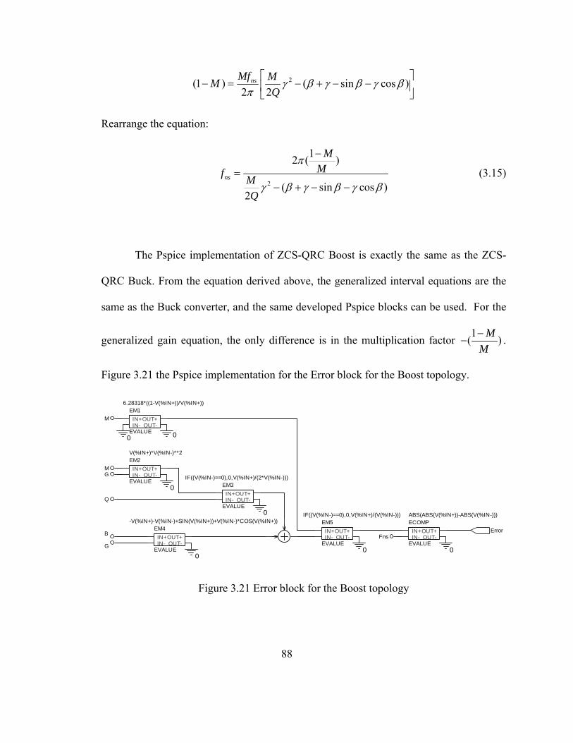
2(1 ) ( sin cos )2 2
nsMf MMQγ β γ β γ β
π⎡ ⎤
− = − + − −⎢ ⎥⎣ ⎦
Rearrange the equation:
2
12 ( )
( sin cos2
ns
MMf M
Q
π
)γ β γ β γ β
−
=− + − −
(3.15)
The Pspice implementation of ZCS-QRC Boost is exactly the same as the ZCS-
QRC Buck. From the equation derived above, the generalized interval equations are the
same as the Buck converter, and the same developed Pspice blocks can be used. For the
generalized gain equation, the only difference is in the multiplication factor 1( )MM−
− .
Figure 3.21 the Pspice implementation for the Error block for the Boost topology.
Error
0
M
0
0G
0
B
M
0
FnsEM4
-V(%IN+)-V(%IN-)+SIN(V(%IN+))+V(%IN-)*COS(V(%IN+))
EVALUE
OUT+OUT-
IN+IN-
0
0
EM2V(%IN+)*V(%IN-)**2
EVALUE
OUT+OUT-
IN+IN-
Q
ECOMPABS(ABS(V(%IN+))-ABS(V(%IN-)))
EVALUE
OUT+OUT-
IN+IN-
G
EM16.28318*((1-V(%IN+))/V(%IN+))
EVALUE
OUT+OUT-
IN+IN-
EM5IF((V(%IN-)==0),0,V(%IN+)/(V(%IN-)))
EVALUE
OUT+OUT-
IN+IN-
EM3IF((V(%IN-)==0),0,V(%IN+)/(2*V(%IN-)))
EVALUE
OUT+OUT-
IN+IN-
Figure 3.21 Error block for the Boost topology
88
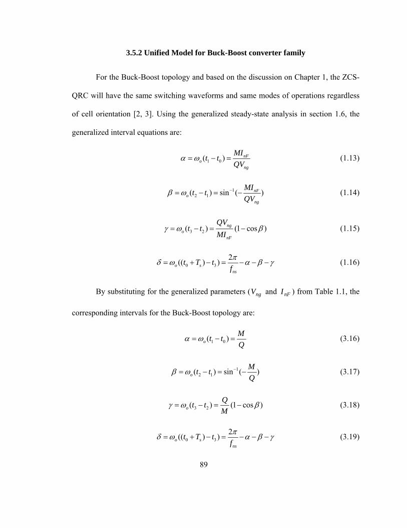
3.5.2 Unified Model for Buck-Boost converter family
For the Buck-Boost topology and based on the discussion on Chapter 1, the ZCS-
QRC will have the same switching waveforms and same modes of operations regardless
of cell orientation [2, 3]. Using the generalized steady-state analysis in section 1.6, the
generalized interval equations are:
1 0( ) nFo
ng
MIt tQV
α ω= − = (1.13)
12 1( ) sin ( nF
ong
)MIt tQV
β ω −= − = − (1.14)
3 2( ) (1 cosngo
nF
QVt t
MI)γ ω= − = − β (1.15)
0 32(( ) )o s
ns
t T tfπδ ω= + − = − −α β γ− (1.16)
By substituting for the generalized parameters ( and ) from Table 1.1, the
corresponding intervals for the Buck-Boost topology are:
ngV nFI
1 0( )oMt tQ
α ω= − = (3.16)
12 1( ) sin (o )Mt t
Qβ ω −= − = − (3.17)
3 2( ) (1 cosoQt tM
)γ ω= − = − β (3.18)
0 32(( ) )o s
ns
t T tfπδ ω= + − = − −α β γ− (3.19)
89
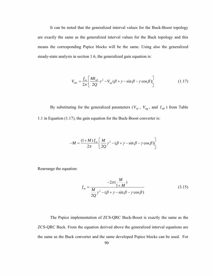
It can be noted that the generalized interval values for the Buck-Boost topology
are exactly the same as the generalized interval values for the Buck topology and this
means the corresponding Pspice blocks will be the same. Using also the generalized
steady-state analysis in section 1.6, the generalized gain equation is:
2 ( sin cos2 2
ns nFnbc ng
f MIV VQ
)γ β γ β γ βπ⎡ ⎤
= − + − −⎢ ⎥⎣ ⎦
(1.17)
By substituting for the generalized parameters ( , , and ) from Table
1.1 in Equation (1.17), the gain equation for the Buck-Boost converter is:
nFV ngV nFI
2(1 ) ( sin cos2 2
nsM f MMQ
)γ β γ β γ βπ
⎡ ⎤+− = − + − −⎢ ⎥
⎣ ⎦
Rearrange the equation:
2
2 ( )1
( sin cos2
ns
MMf M
Q
π
)γ β γ β γ β
−+=
− + − − (3.15)
The Pspice implementation of ZCS-QRC Buck-Boost is exactly the same as the
ZCS-QRC Buck. From the equation derived above the generalized interval equations are
the same as the Buck converter and the same developed Pspice blocks can be used. For
90
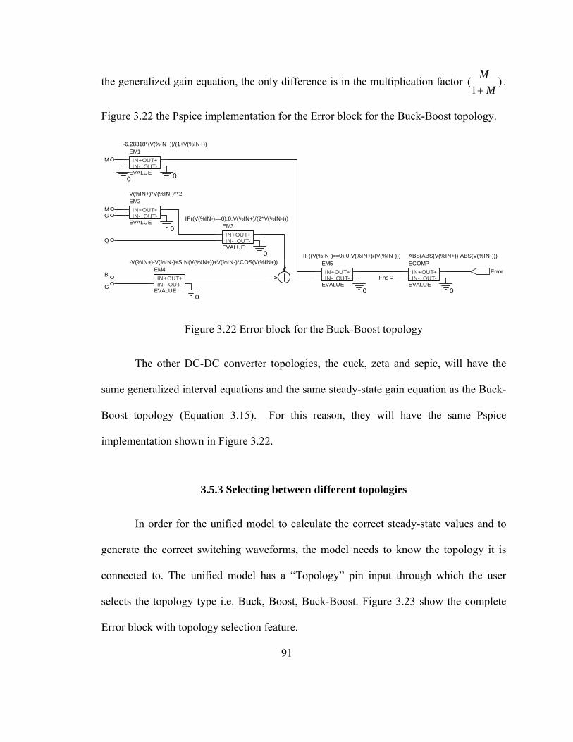
the generalized gain equation, the only difference is in the multiplication factor ( )1
MM+
.
Figure 3.22 the Pspice implementation for the Error block for the Buck-Boost topology.
Error
0
M
0
0G
0
B
M
0
FnsEM4
-V(%IN+)-V(%IN-)+SIN(V(%IN+))+V(%IN-)*COS(V(%IN+))
EVALUE
OUT+OUT-
IN+IN-
0
0
EM2V(%IN+)*V(%IN-)**2
EVALUE
OUT+OUT-
IN+IN-
Q
ECOMPABS(ABS(V(%IN+))-ABS(V(%IN-)))
EVALUE
OUT+OUT-
IN+IN-
G
EM1-6.28318*(V(%IN+))/(1+V(%IN+))
EVALUE
OUT+OUT-
IN+IN-
EM5IF((V(%IN-)==0),0,V(%IN+)/(V(%IN-)))
EVALUE
OUT+OUT-
IN+IN-
EM3IF((V(%IN-)==0),0,V(%IN+)/(2*V(%IN-)))
EVALUE
OUT+OUT-
IN+IN-
Figure 3.22 Error block for the Buck-Boost topology
The other DC-DC converter topologies, the cuck, zeta and sepic, will have the
same generalized interval equations and the same steady-state gain equation as the Buck-
Boost topology (Equation 3.15). For this reason, they will have the same Pspice
implementation shown in Figure 3.22.
3.5.3 Selecting between different topologies
In order for the unified model to calculate the correct steady-state values and to
generate the correct switching waveforms, the model needs to know the topology it is
connected to. The unified model has a “Topology” pin input through which the user
selects the topology type i.e. Buck, Boost, Buck-Boost. Figure 3.23 show the complete
Error block with topology selection feature.
91
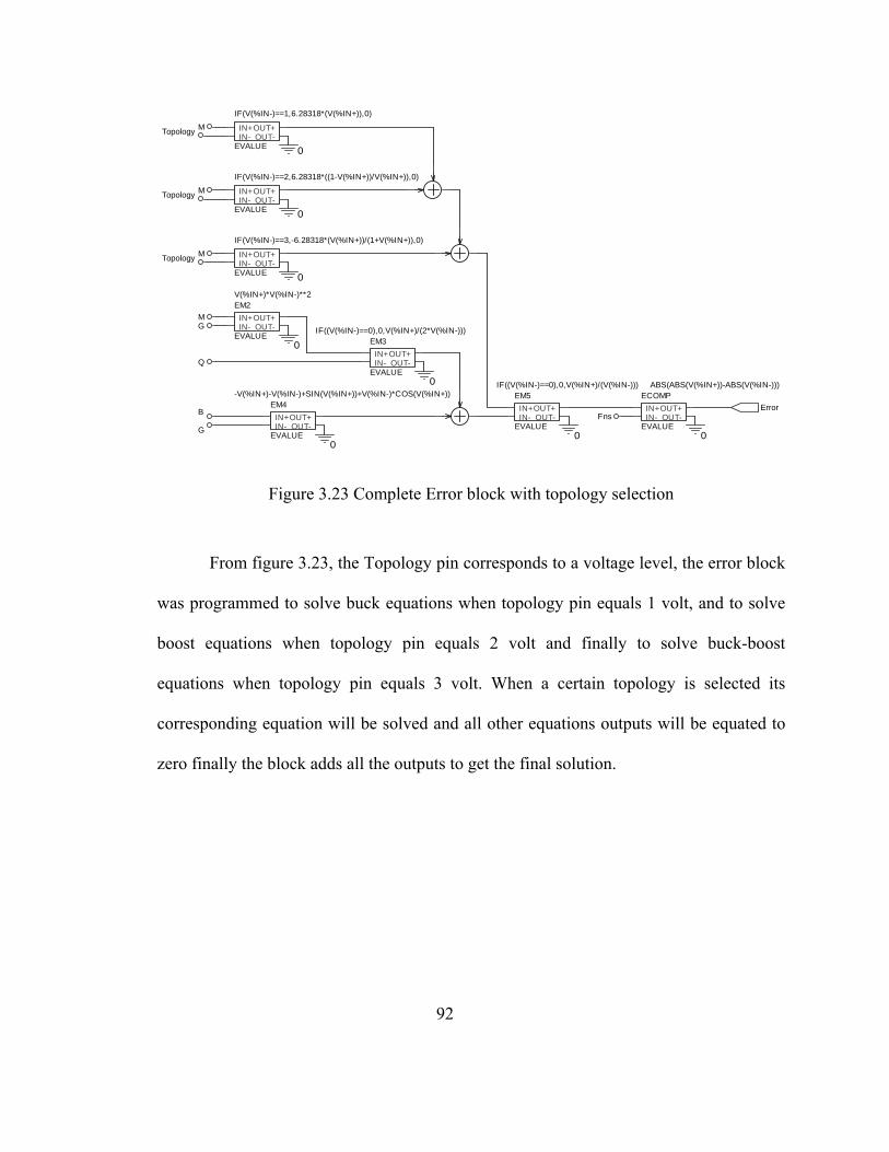
M
EM2V(%IN+)*V(%IN-)**2
EVALUE
OUT+OUT-
IN+IN-
0
G
M
ECOMPABS(ABS(V(%IN+))-ABS(V(%IN-)))
EVALUE
OUT+OUT-
IN+IN-
Q
0
0
IF(V(%IN-)==2,6.28318*((1-V(%IN+))/V(%IN+)),0)
EVALUE
OUT+OUT-
IN+IN-
0
IF(V(%IN-)==1,6.28318*(V(%IN+)),0)
EVALUE
OUT+OUT-
IN+IN-
B
Topology
EM3IF((V(%IN-)==0),0,V(%IN+)/(2*V(%IN-)))
EVALUE
OUT+OUT-
IN+IN-
0
Topology
GM
Topology
Fns
00
EM5IF((V(%IN-)==0),0,V(%IN+)/(V(%IN-)))
EVALUE
OUT+OUT-
IN+IN-
0
EM4-V(%IN+)-V(%IN-)+SIN(V(%IN+))+V(%IN-)*COS(V(%IN+))
EVALUE
OUT+OUT-
IN+IN-
M
Error
IF(V(%IN-)==3,-6.28318*(V(%IN+))/(1+V(%IN+)),0)
EVALUE
OUT+OUT-
IN+IN-
Figure 3.23 Complete Error block with topology selection
From figure 3.23, the Topology pin corresponds to a voltage level, the error block
was programmed to solve buck equations when topology pin equals 1 volt, and to solve
boost equations when topology pin equals 2 volt and finally to solve buck-boost
equations when topology pin equals 3 volt. When a certain topology is selected its
corresponding equation will be solved and all other equations outputs will be equated to
zero finally the block adds all the outputs to get the final solution.
92
93
CHAPTER 4
CONCLUSION
4.1 Summary
This thesis presents a unified steady-state model for soft-switching converters; the
unified model is an easy and versatile way to simulate soft-switching and other
complicated topologies. Also, the unified model provides designers with a better
understanding of soft-switching topologies and offers a fast steady-state solution in
addition to providing accurate waveforms for different cell parameters and state-plane
diagrams. It is also a good educational tool.
The unified model is based on generalized analysis which is a new technique to
analyze and to find steady-state solutions for soft-switching cells. Generalized analysis is
based on the idea that soft-switching cells will have the same modes of operation and the
same switching waveforms in spite of cell orientation. So instead of analyzing switching
cells contained in different converters as a one topology, only the switching cell needs to
be analyzed and the result can be applied to different DC-DC converter families using
transformation tables. To introduce unified model development issues and challenges, the
zero current switching (ZCS) quasi-resonant (QRC) unified switching cell was selected.
The proposed unified simulation model is implemented in Pspice/Orcad®
simulation software to provide a model that can be used as a part of complete simulation
schematic that may include other models in Pspice/Orcad®. Using the mathematical
equations approach to implement the model requires the ability to implement
programming loops and to perform instructions in a certain sequence, which was the main
challenge in this work because Pspice/Orcad® is not a programming language and soft –
switching cells have complicated set of equations that describe the operation modes.
The unified steady-state model is useful in soft-switching cells analysis and
design; the user connects the simulation model to the desired topology configuration and
the Model calculates the steady-state gain solution for the user. The model also provides
the user with different necessary plots needed for soft-switching cell design. This
includes the internal switching cell information such as switching cell inductor current
LrI and the switching cell capacitor voltage , and their corresponding state-plane
diagram. The model can also be used in feed-back design applications where the output
voltage is regulated by changing the switching frequency.
CrV
4.2 Future work
Future work will focus on optimizing the unified model accuracy and speed. The
model speed can be increased by implementing fast numerical techniques to solve the
unified equation non-linear equation. Model accuracy can be increased by searching for
the error signal minimum point instead of using a threshold value. Feed-back design
using the unified model is still in its early stages. It needs more research and work.
94
95
REFERENCES
[1] I. Batarseh, “Power Electronics Circuits,” John Wiley, Fall 2000. [2] J. Abu-Qahouq, “Generalized Analysis of Soft-Switching DC-DC Converters
Families,” Master Thesis, University of Central Florida,2000. [3] J. Abu-Qahouq, I. Batarseh, “Unified steady-state analysis of soft-switching DC-DC
converters,” IEEE Trans. Power Electron. vol. 17, pp. 684 - 691, Sept. 2002. [4] G. Hua, “Soft-Switching Techniques for Pulse-Width-Modulated Converters,”
Virginia Power Electronics Center, 1994. [5] G. Hua, F.C. Lee, “An overview of soft-switching techniques for PWM converters,”
EPE Journal, vol. 3, no. 1, March 1993. [6] G. Hua, F.C. Lee, “Soft-switching techniques for PWM converters,” International
Conf. on Industrial Electronics, Control and Instrumentation, 1993. [7] G. Hua and F. Lee “Evaluation of Switched-Mode Power conversion Topologies,”
The first international Power Electronics and Motion Control Conf. (IPEMC), Vol.1, pp.12-26,1994.
[8] E.J. Miller “Resonant Switching Power Conversion,” IEEE Power Electronics
Specialists conference Rec. pp. 206-211, 1976. [9] K. Liu, R. Oruganti, and F. C. Lee, “Resonant Switches – Topologies and
Characteristics,” IEEE Trans. On Power Electronics, Vol. PE-2, No.1, pp. 62-74, 1987.
[10] T. Mizoguchi, T. Ohgai, and T. Ninomiya, “A Family of Single-Switch ZVS-CV
DC-DC Converters,” IEEE Applied Power Electronics Specialists Conf. Vol. 2, pp. 1392-1398,1994.
[11] C.P. Henze, H.C. Martin, D.W. Parsley, “Zero-voltage-switching in high
frequency power converters using pulse width modulation,” IEEE Applied Power Electronics Conf. Proc., pp. 33-40, 1988.

96
[12] Treviso, C.H.G., De Freitas, O.C., and Farias V.J., “A ZVS-ZCS-PWM self resonant DC-DC Sepic converter,” Industrial Electronics, Control and Instrumentation, Vol. 1, pp. 176 – 181,1994.
[13] V. Vorperian, “Quasi-Square-wave Converters: Topologies and Analysis,” IEEE
Trans. On Power Electronics, Vol. 3, No. 2, pp. 183-191,1998. [14] V. Vorperian, R. Tymerski; F.C.Y Lee, “Equivalent circuit models for resonant
and PWM switches,” IEEE Trans. On Power Electronics, Vol. 4, pp. 205 - 214,1989. [15] V. Vorperian, W.T. McLyman, “Analysis of a PWM-resonant converter,” IEEE
Trans. On Aerospace and Electronic Systems, Vol. 33, pp. 163 - 170, 1997. [16] S.G. Trabert, R.W. Erickson, “Steady state analysis of the duty cycle controlled
series resonant converter,” IEEE Power Electronics Specialists Conf. Rec., pp. 545-556,1987.
[17] OrCAD Pspice User’s Guide. [18] OrCAD Capture User’s Guide. [19] MicroSim Application Notes. [20] M. Cotorogea , “Using analog behavioral modeling in PSpice for the
implementation of subcircuit-models of power devices,” IEEE International Power Electronics Congress, CIEP 98, pp. 158 - 163, 1998.
[21] http://mathworld.wolfram.com/SeriesExpansion.html. [22] http://mathworld.wolfram.com/MaclaurinSeries.html. [23] Daniel Zwillinger, “CRC Standard Mathematical Tables and Formulae,” 31st
Edition, John Wiley, November 2002. [24] M. Cotorogea , “Implementation of mathematical models of power devices for
circuit simulation in Pspice,” 6th Workshop on Computers in Power Electronics, 1998. pp. 17 - 22, 1998.
97
[25] N.D Muhamad, A.J Shafie , “An approach to Pspice-aided control loop design of DC-DC converter systems,” Power and Energy Conference, PECon, pp. 121 - 126, 2003.
[26] N.D Muhamad, A.J Shafie , “A PSPICE-based design of DC-DC converter
systems,” Power and Energy Conference, PECon, pp. 73 - 77, 2004. [27] M.K Kazimierczuk, W.D Morse, “State-plane analysis of zero-current-switching
resonant DC/DC power converters,” IEEE Transactions on Power Electronics, Volume 4, pp 265 – 271, 1989.
[28] M.K Kazimierczuk, W.D Morse, “State-plane analysis of zero-voltage-switching
resonant DC/DC power converters,” IEEE Transactions on Power Electronics, Volume 24, pp 232-240, 1989.
[29] Naser Kutkut, C. Q. Lee and Issa Batarseh “A Generalized Program For
Extracting the Control Characteristcs of Resonant Converters via State-Plane Diagram,” IEEE. PP. 1236-1242, 1995.
[30] A. Alsharqawi, “Steady State Analysis of Softs Switching DC-DC and MAGAMP
Forward Converters,” Master Thesis, University of Central Florida,2002. [31] A. Alsharqawi, I. Batarseh, “Generalized state-plane analysis of softswitching
DC-DC converters,” , IEEE International Symposium on Circuits and Systems (ISCAS), 2002.
[32] W. Al-Hoor, J. Abu-Qahouq and I. Batarseh, “Unified steady-state computer
aided Model for soft-switching DC-DC converters,” IEEE Applied Power Electronics Conference (APEC),2006.
Related Documents


