Juan Gómez Luna , Izzat El Hajj, Ivan Fernandez, Christina Giannoula, Geraldo F. Oliveira, Onur Mutlu Understanding a Modern Processing-in-Memory Architecture: Benchmarking and Experimental Characterization https://arxiv.org/pdf/2105.03814.pdf https://github.com/CMU-SAFARI/prim-benchmarks

Welcome message from author
This document is posted to help you gain knowledge. Please leave a comment to let me know what you think about it! Share it to your friends and learn new things together.
Transcript

Juan Gómez Luna, Izzat El Hajj, Ivan Fernandez, Christina Giannoula,
Geraldo F. Oliveira, Onur Mutlu
Understanding a Modern Processing-in-Memory Architecture:Benchmarking and Experimental Characterization
https://arxiv.org/pdf/2105.03814.pdfhttps://github.com/CMU-SAFARI/prim-benchmarks

2
Executive Summary• Data movement between memory/storage units and compute units is a major
contributor to execution time and energy consumption• Processing-in-Memory (PIM) is a paradigm that can tackle the data movement
bottleneck- Though explored for +50 years, technology challenges prevented the successful materialization
• UPMEM has designed and fabricated the first publicly-available real-world PIM architecture- DDR4 chips embedding in-order multithreaded DRAM Processing Units (DPUs)
• Our work:- Introduction to UPMEM programming model and PIM architecture- Microbenchmark-based characterization of the DPU- Benchmarking and workload suitability study
• Main contributions:- Comprehensive characterization and analysis of the first commercially-available PIM architecture- PrIM (Processing-In-Memory) benchmarks:
• 16 workloads that are memory-bound in conventional processor-centric systems• Strong and weak scaling characteristics
- Comparison to state-of-the-art CPU and GPU
• Takeaways:- Workload characteristics for PIM suitability- Programming recommendations- Suggestions and hints for hardware and architecture designers of future PIM systems- PrIM: (a) programming samples, (b) evaluation and comparison of current and future PIM systems

3
Data Movement in Computing Systems• Data movement dominates performance and is a major system
energy bottleneck• Total system energy: data movement accounts for
- 62% in consumer applications✻, - 40% in scientific applications★, - 35% in mobile applications☆
✻Boroumand et al., “Google Workloads for Consumer Devices: Mitigating Data Movement Bottlenecks,” ASPLOS 2018★Kestor et al., “Quantifying the Energy Cost of Data Movement in Scientific Applications,” IISWC 2013 ☆Pandiyan and Wu, “Quantifying the energy cost of data movement for emerging smart phone workloads on mobile platforms,” IISWC 2014
DRAM
Data Movement
GPU
CPUCPU
SoC
L2
Video Decoder
Video Encoder
Audio Display Engine

4
Data Movement in Computing Systems• Data movement dominates performance and is a major system
energy bottleneck• Total system energy: data movement accounts for
- 62% in consumer applications✻, - 40% in scientific applications★, - 35% in mobile applications☆
✻Boroumand et al., “Google Workloads for Consumer Devices: Mitigating Data Movement Bottlenecks,” ASPLOS 2018★Kestor et al., “Quantifying the Energy Cost of Data Movement in Scientific Applications,” IISWC 2013 ☆Pandiyan and Wu, “Quantifying the energy cost of data movement for emerging smart phone workloads on mobile platforms,” IISWC 2014
DRAM
Data Movement
GPU
CPUCPU
SoC
L2
Video Decoder
Video Encoder
Audio Display Engine
Processing-In-Memory proposes computing where it makes sense
(where data resides)
Compute systems should be more data-centric
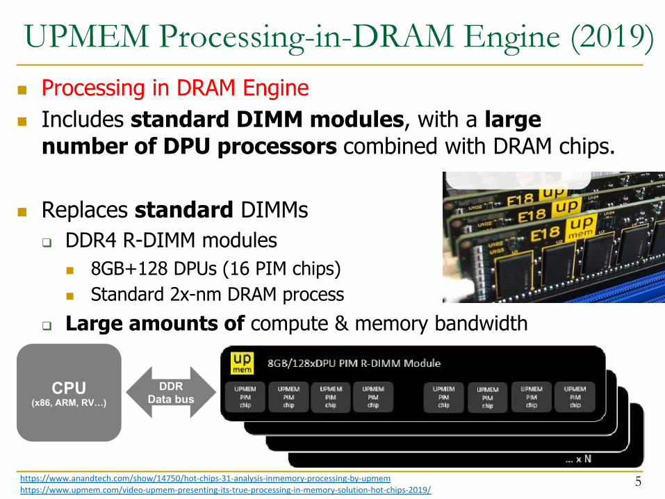
UPMEM Processing-in-DRAM Engine (2019)
5
n Processing in DRAM Engine n Includes standard DIMM modules, with a large
number of DPU processors combined with DRAM chips.
n Replaces standard DIMMsq DDR4 R-DIMM modules
n 8GB+128 DPUs (16 PIM chips)n Standard 2x-nm DRAM process
q Large amounts of compute & memory bandwidth
https://www.anandtech.com/show/14750/hot-chips-31-analysis-inmemory-processing-by-upmemhttps://www.upmem.com/video-upmem-presenting-its-true-processing-in-memory-solution-hot-chips-2019/
CPU(x86, ARM, RV…)
DDRData bus

6
Understanding a Modern PIM Architecture
https://arxiv.org/pdf/2105.03814.pdfhttps://github.com/CMU-SAFARI/prim-benchmarks

7
Observations, Recommendations, TakeawaysGENERALPROGRAMMINGRECOMMENDATIONS1. ExecuteontheDRAMProcessingUnits (DPUs)
portionsofparallelcode thatareaslongaspossible.2. Splittheworkloadintoindependentdatablocks,
whichtheDPUsoperateonindependently.3. UseasmanyworkingDPUsinthesystemaspossible.4. Launchatleast11tasklets (i.e.,softwarethreads)
perDPU.
PROGRAMMINGRECOMMENDATION1FordatamovementbetweentheDPU’sMRAMbankandtheWRAM,uselargeDMAtransfersizeswhenalltheaccesseddataisgoingtobeused.
KEYOBSERVATION7
LargerCPU-DPUandDPU-CPUtransfersbetweenthehostmainmemoryandtheDRAMProcessingUnit’sMainmemory(MRAM)banksresultinhighersustainedbandwidth. KEYTAKEAWAY1
TheUPMEMPIMarchitectureisfundamentallycomputebound.Asaresult,themostsuitablework- loadsarememory-bound.

8
PrIM Repository• All microbenchmarks, benchmarks, and scripts• https://github.com/CMU-SAFARI/prim-benchmarks
9
Outline• Introduction
- Accelerator Model- UPMEM-based PIM System Overview
• UPMEM PIM Programming- Vector Addition- CPU-DPU Data Transfers- Inter-DPU Communication- CPU-DPU/DPU-CPU Transfer Bandwidth
• DRAM Processing Unit- Arithmetic Throughput- WRAM and MRAM Bandwidth
• PrIM Benchmarks- Roofline Model- Benchmark Diversity
• Evaluation- Strong and Weak Scaling- Comparison to CPU and GPU
• Key Takeaways

10
Outline• Introduction
- Accelerator Model- UPMEM-based PIM System Overview
• UPMEM PIM Programming- Vector Addition- CPU-DPU Data Transfers- Inter-DPU Communication- CPU-DPU/DPU-CPU Transfer Bandwidth
• DRAM Processing Unit- Arithmetic Throughput- WRAM and MRAM Bandwidth
• PrIM Benchmarks- Roofline Model- Benchmark Diversity
• Evaluation- Strong and Weak Scaling- Comparison to CPU and GPU
• Key Takeaways

11
Accelerator Model• UPMEM DIMMs coexist with conventional DIMMs
• Integration of UPMEM DIMMs in a system follows an accelerator model
• UPMEM DIMMs can be seen as a loosely coupled accelerator- Explicit data movement between the main processor (host
CPU) and the accelerator (UPMEM)- Explicit kernel launch onto the UPMEM processors
• This resembles GPU computing

12
System Organization (I)• In a UPMEM-based PIM system UPMEM DIMMs coexist
with regular DDR4 DIMMs
Host CPU
xN
PIM Chip
PIM Chip
PIM Chip
PIM Chip
PIM Chip
PIM Chip
PIM Chip
PIM Chip
PIM Chip
PIM Chip
PIM Chip
PIM Chip
PIM Chip
PIM Chip
PIM Chip
PIM Chip
xM
DRAM Chip
DRAM Chip
DRAM Chip
DRAM Chip
DRAM Chip
DRAM Chip
DRAM Chip
DRAM Chip
DRAM Chip
DRAM Chip
DRAM Chip
DRAM Chip
DRAM Chip
DRAM Chip
DRAM Chip
DRAM Chip
Main Memory
PIM-enabled Memory
13
Host CPU
xN
PIM Chip
PIM Chip
PIM Chip
PIM Chip
PIM Chip
PIM Chip
PIM Chip
PIM Chip
PIM Chip
PIM Chip
PIM Chip
PIM Chip
PIM Chip
PIM Chip
PIM Chip
PIM Chip
xM
DRAM Chip
DRAM Chip
DRAM Chip
DRAM Chip
DRAM Chip
DRAM Chip
DRAM Chip
DRAM Chip
DRAM Chip
DRAM Chip
DRAM Chip
DRAM Chip
DRAM Chip
DRAM Chip
DRAM Chip
DRAM Chip
Main Memory
PIM-enabled Memory
PIM Chip
x8
Control/Status Interface DDR4 Interface
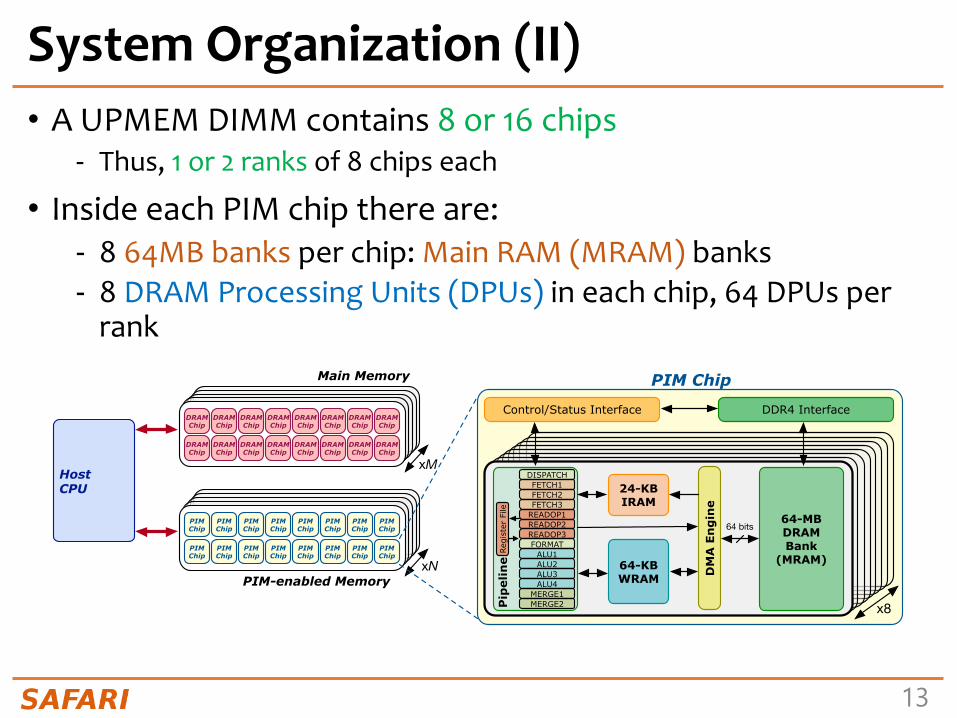
System Organization (II)• A UPMEM DIMM contains 8 or 16 chips
- Thus, 1 or 2 ranks of 8 chips each
• Inside each PIM chip there are:- 8 64MB banks per chip: Main RAM (MRAM) banks- 8 DRAM Processing Units (DPUs) in each chip, 64 DPUs per
rank
24-KB IRAM
DM
A E
ng
ine
64-KB WRAM
DISPATCHFETCH1FETCH2FETCH3
READOP1READOP2READOP3FORMAT
ALU1ALU2ALU3ALU4
MERGE1MERGE2
Regi
ster
File
Pip
elin
e64-MB DRAM Bank
(MRAM)
64 bits

14
Host CPU 0
x10
PIM Chip
PIM Chip
PIM Chip
PIM Chip
PIM Chip
PIM Chip
PIM Chip
PIM Chip
PIM Chip
PIM Chip
PIM Chip
PIM Chip
PIM Chip
PIM Chip
PIM Chip
PIM Chip
x2
DRAM Chip
DRAM Chip
DRAM Chip
DRAM Chip
DRAM Chip
DRAM Chip
DRAM Chip
DRAM Chip
DRAM Chip
DRAM Chip
DRAM Chip
DRAM Chip
DRAM Chip
DRAM Chip
DRAM Chip
DRAM Chip
Main Memory
PIM-enabled Memory
Host CPU 1
x10
PIM Chip
PIM Chip
PIM Chip
PIM Chip
PIM Chip
PIM Chip
PIM Chip
PIM Chip
PIM Chip
PIM Chip
PIM Chip
PIM Chip
PIM Chip
PIM Chip
PIM Chip
PIM Chip
x2
DRAM Chip
DRAM Chip
DRAM Chip
DRAM Chip
DRAM Chip
DRAM Chip
DRAM Chip
DRAM Chip
DRAM Chip
DRAM Chip
DRAM Chip
DRAM Chip
DRAM Chip
DRAM Chip
DRAM Chip
DRAM Chip
Main Memory
PIM-enabled Memory
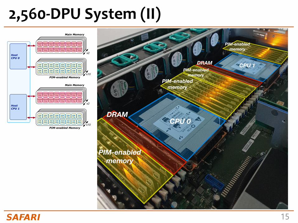
2,560-DPU System (I)• UPMEM-based PIM
system with 20 UPMEM DIMMs of 16 chips each (40 ranks)- P21 DIMMs- Dual x86 socket
• UPMEM DIMMscoexist with regular DDR4 DIMMs
• 2 memory controllers/socket (3 channels each)
• 2 conventional DDR4 DIMMs on one channel of one controller
2560 DPUs*
* There are 4 faulty DPUs in the system that we use in our experiments. Thus, the maximum number of DPUs we can use is 2,556.
160 GB
15
2,560-DPU System (II)
CPU 0
CPU 1
DRAM
DRAM
PIM-enabled memory
PIM-enabled memory
PIM-enabled memory
PIM-enabled memory
Host CPU 0
x10
PIM Chip
PIM Chip
PIM Chip
PIM Chip
PIM Chip
PIM Chip
PIM Chip
PIM Chip
PIM Chip
PIM Chip
PIM Chip
PIM Chip
PIM Chip
PIM Chip
PIM Chip
PIM Chip
x2
DRAM Chip
DRAM Chip
DRAM Chip
DRAM Chip
DRAM Chip
DRAM Chip
DRAM Chip
DRAM Chip
DRAM Chip
DRAM Chip
DRAM Chip
DRAM Chip
DRAM Chip
DRAM Chip
DRAM Chip
DRAM Chip
Main Memory
PIM-enabled Memory
Host CPU 1
x10
PIM Chip
PIM Chip
PIM Chip
PIM Chip
PIM Chip
PIM Chip
PIM Chip
PIM Chip
PIM Chip
PIM Chip
PIM Chip
PIM Chip
PIM Chip
PIM Chip
PIM Chip
PIM Chip
x2
DRAM Chip
DRAM Chip
DRAM Chip
DRAM Chip
DRAM Chip
DRAM Chip
DRAM Chip
DRAM Chip
DRAM Chip
DRAM Chip
DRAM Chip
DRAM Chip
DRAM Chip
DRAM Chip
DRAM Chip
DRAM Chip
Main Memory
PIM-enabled Memory

16
640-DPU System• UPMEM-based PIM
system with 10 UPMEM DIMMs of 8 chips each (10 ranks)- E19 DIMMs- x86 socket
• 2 memory controllers (3 channels each)
• 2 conventional DDR4 DIMMs on one channel of one controller
Host CPU
x10
PIM Chip
PIM Chip
PIM Chip
PIM Chip
PIM Chip
PIM Chip
PIM Chip
PIM Chip
PIM Chip
PIM Chip
PIM Chip
PIM Chip
PIM Chip
PIM Chip
PIM Chip
PIM Chip
x2
DRAM Chip
DRAM Chip
DRAM Chip
DRAM Chip
DRAM Chip
DRAM Chip
DRAM Chip
DRAM Chip
DRAM Chip
DRAM Chip
DRAM Chip
DRAM Chip
DRAM Chip
DRAM Chip
DRAM Chip
DRAM Chip
Main Memory
PIM-enabled Memory
640 DPUs
40 GB

17
Outline• Introduction
- Accelerator Model- UPMEM-based PIM System Overview
• UPMEM PIM Programming- Vector Addition- CPU-DPU Data Transfers- Inter-DPU Communication- CPU-DPU/DPU-CPU Transfer Bandwidth
• DRAM Processing Unit- Arithmetic Throughput- WRAM and MRAM Bandwidth
• PrIM Benchmarks- Roofline Model- Benchmark Diversity
• Evaluation- Strong and Weak Scaling- Comparison to CPU and GPU
• Key Takeaways

18
Vector Addition (VA)• Our first programming example• We partition the input arrays across:
- DPUs- Tasklets, i.e., software threads running on a DPU
A[0] A[1] A[N-1]
B[0] B[1] B[N-1]
C[0] C[1] C[N-1]
DPU 0 DPU 1 DPU 2 DPU 3
Tasklet0
Tasklet1
Tasklet0
Tasklet1
Tasklet0
Tasklet1
Tasklet0
Tasklet1

19
General Programming Recommendations
• From UPMEM programming guide✻, presentations★, and white papers☆
✻https://sdk.upmem.com/2021.1.1/index.html★ F. Devaux, "The true Processing In Memory accelerator," HotChips 2019. doi: 10.1109/HOTCHIPS.2019.8875680☆UPMEM, “Introduction to UPMEM PIM. Processing-in-memory (PIM) on DRAM Accelerator,” White paper
GENERALPROGRAMMINGRECOMMENDATIONS1. ExecuteontheDRAMProcessingUnits (DPUs)
portionsofparallelcode thatareaslongaspossible.
2. Splittheworkloadintoindependentdatablocks,whichtheDPUsoperateonindependently.
3. UseasmanyworkingDPUsinthesystemaspossible.
4. Launchatleast11tasklets (i.e.,softwarethreads) perDPU.

20
CPU-DPU/DPU-CPU Data Transfers• CPU-DPU and DPU-CPU transfers
- Between host CPU’s main memory and DPUs’ MRAM banks
• Serial CPU-DPU/DPU-CPU transfers: - A single DPU (i.e., 1 MRAM bank)
• Parallel CPU-DPU/DPU-CPU transfers: - Multiple DPUs (i.e., many MRAM banks)
• Broadcast CPU-DPU transfers: - Multiple DPUs with a single buffer
Host CPU
xN
PIM Chip
PIM Chip
PIM Chip
PIM Chip
PIM Chip
PIM Chip
PIM Chip
PIM Chip
PIM Chip
PIM Chip
PIM Chip
PIM Chip
PIM Chip
PIM Chip
PIM Chip
PIM Chip
xM
DRAM Chip
DRAM Chip
DRAM Chip
DRAM Chip
DRAM Chip
DRAM Chip
DRAM Chip
DRAM Chip
DRAM Chip
DRAM Chip
DRAM Chip
DRAM Chip
DRAM Chip
DRAM Chip
DRAM Chip
DRAM Chip
Main Memory
PIM-enabled Memory
CPU-D
PU
DPU-CPU
21
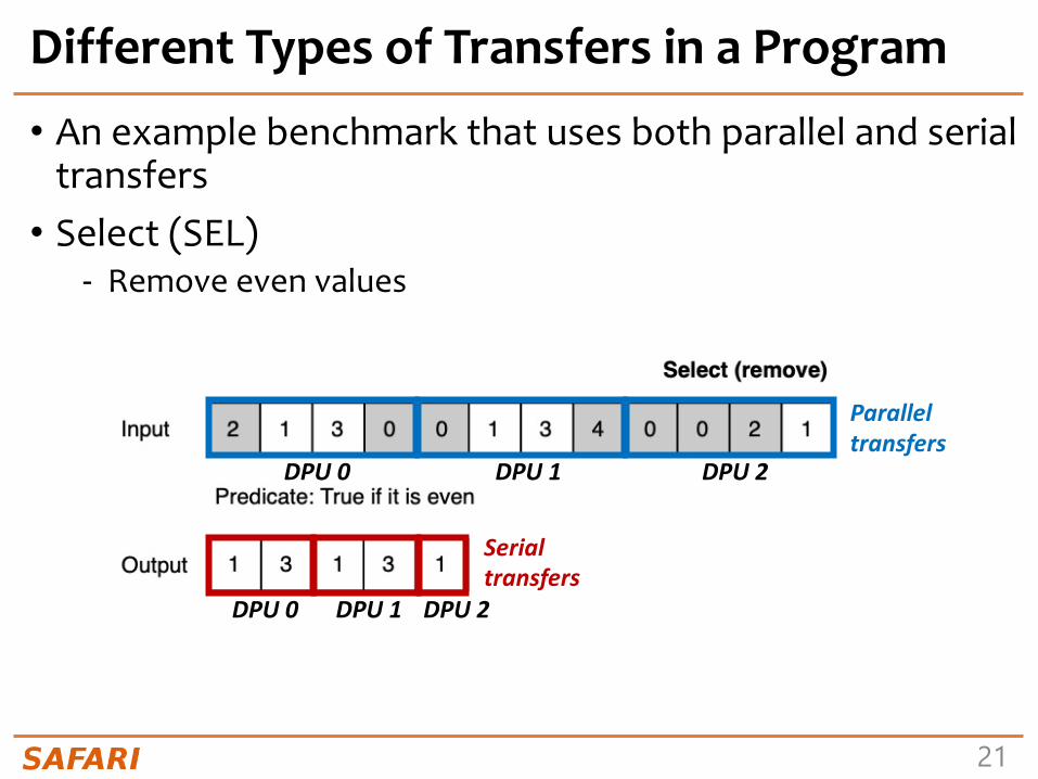
Different Types of Transfers in a Program
• An example benchmark that uses both parallel and serial transfers• Select (SEL)
- Remove even values
DPU 0 DPU 1 DPU 2
DPU 0 DPU 1 DPU 2
Parallel transfers
Serial transfers
22
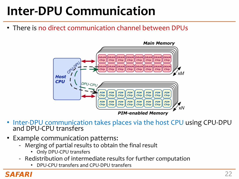
Inter-DPU Communication• There is no direct communication channel between DPUs
• Inter-DPU communication takes places via the host CPU using CPU-DPU and DPU-CPU transfers
• Example communication patterns:- Merging of partial results to obtain the final result
• Only DPU-CPU transfers- Redistribution of intermediate results for further computation
• DPU-CPU transfers and CPU-DPU transfers
Host CPU
xN
PIM Chip
PIM Chip
PIM Chip
PIM Chip
PIM Chip
PIM Chip
PIM Chip
PIM Chip
PIM Chip
PIM Chip
PIM Chip
PIM Chip
PIM Chip
PIM Chip
PIM Chip
PIM Chip
xM
DRAM Chip
DRAM Chip
DRAM Chip
DRAM Chip
DRAM Chip
DRAM Chip
DRAM Chip
DRAM Chip
DRAM Chip
DRAM Chip
DRAM Chip
DRAM Chip
DRAM Chip
DRAM Chip
DRAM Chip
DRAM Chip
Main Memory
PIM-enabled Memory
CPU-D
PU
DPU-CPU

23
How Fast are these Data Transfers? • With a microbenchmark, we obtain the sustained
bandwidth of all types of CPU-DPU and DPU-CPU transfers• Two experiments:
- 1 DPU: variable CPU-DPU and DPU-CPU transfer size (8 bytes to 32 MB)
- 1 rank: 32 MB CPU-DPU and DPU-CPU transfers to/from a set of 1 to 64 MRAM banks within the same rank
• We do not experiment with more than one rank- Preliminary experiments show that the UPMEM SDK* only
parallelizes transfers within the same rank
* UPMEM SDK 2021.1.1
DDR4 bandwidth bounds the maximum transfer bandwidth
The cost of the transfers can be amortized, if enough computation is run on the DPUs

24
CPU-DPU/DPU-CPU Transfers: 1 DPU• Data transfer size varies between 8 bytes and 32 MB
0.0001
0.0010
0.0100
0.1000
1.0000
8 32 128
512 2K 8K 32K
128K
512K 2M 8M 32M
Sust
aine
d CP
U-D
PU
Band
wid
th(G
B/s,
log
scal
e)
Data transfer size (bytes)
CPU-DPU
DPU-CPU
KEYOBSERVATION7LargerCPU-DPUandDPU-CPUtransfersbetweenthehostmainmemoryandtheDRAMProcessingUnit’sMainmemory(MRAM)banksresultinhighersustainedbandwidth.
25
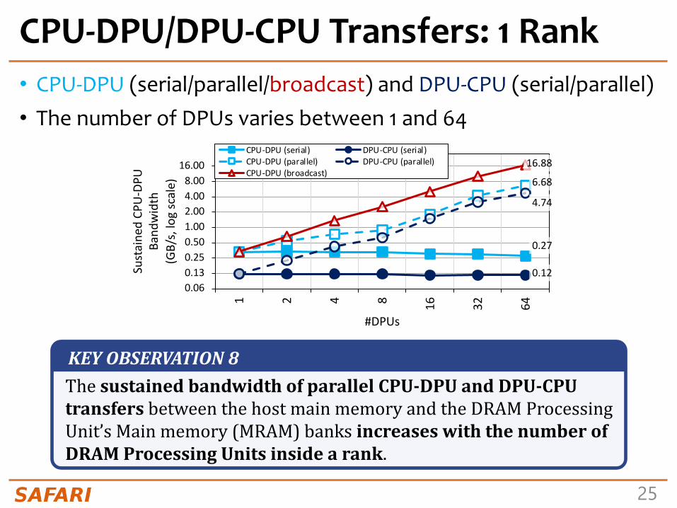
CPU-DPU/DPU-CPU Transfers: 1 Rank• CPU-DPU (serial/parallel/broadcast) and DPU-CPU (serial/parallel)• The number of DPUs varies between 1 and 64
0.27
0.12
6.68
4.74
16.88
0.060.130.250.501.002.004.008.00
16.00
1 2 4 8 16 32 64
Sust
aine
d CP
U-D
PU
Band
wid
th(G
B/s,
log
scal
e)
#DPUs
CPU-DPU (serial) DPU-CPU (serial)CPU-DPU (parallel) DPU-CPU (parallel)CPU-DPU (broadcast)
KEYOBSERVATION8ThesustainedbandwidthofparallelCPU-DPUandDPU-CPUtransfers betweenthehostmainmemoryandtheDRAMProcessingUnit’sMainmemory(MRAM)banksincreaseswiththenumberofDRAMProcessingUnitsinsidearank.

26
CPU-DPU/DPU-CPU Transfers: 1 Rank• CPU-DPU (serial/parallel/broadcast) and DPU-CPU (serial/parallel)• The number of DPUs varies between 1 and 64
0.27
0.12
6.68
4.74
16.88
0.060.130.250.501.002.004.008.00
16.00
1 2 4 8 16 32 64
Sust
aine
d CP
U-D
PU
Band
wid
th(G
B/s,
log
scal
e)
#DPUs
CPU-DPU (serial) DPU-CPU (serial)CPU-DPU (parallel) DPU-CPU (parallel)CPU-DPU (broadcast)
KEYOBSERVATION8ThesustainedbandwidthofparallelCPU-DPUandDPU-CPUtransfers betweenthehostmainmemoryandtheDRAMProcessingUnit’sMainmemory(MRAM)banksincreaseswiththenumberofDRAMProcessingUnitsinsidearank.
https://arxiv.org/pdf/2105.03814.pdfhttps://github.com/CMU-SAFARI/prim-benchmarks
27
Outline• Introduction
- Accelerator Model- UPMEM-based PIM System Overview
• UPMEM PIM Programming- Vector Addition- CPU-DPU Data Transfers- Inter-DPU Communication- CPU-DPU/DPU-CPU Transfer Bandwidth
• DRAM Processing Unit- Arithmetic Throughput- WRAM and MRAM Bandwidth
• PrIM Benchmarks- Roofline Model- Benchmark Diversity
• Evaluation- Strong and Weak Scaling- Comparison to CPU and GPU
• Key Takeaways

28
DRAM Processing Unit
Host CPU
xN
PIM Chip
PIM Chip
PIM Chip
PIM Chip
PIM Chip
PIM Chip
PIM Chip
PIM Chip
PIM Chip
PIM Chip
PIM Chip
PIM Chip
PIM Chip
PIM Chip
PIM Chip
PIM Chip
PIM Chip
24-KB IRAM
DM
A E
ng
ine
64-MB DRAM Bank
(MRAM)64-KB WRAM
x8
Control/Status Interface DDR4 Interface
DISPATCHFETCH1FETCH2FETCH3
READOP1READOP2READOP3FORMAT
ALU1ALU2ALU3ALU4
MERGE1MERGE2
Regi
ster
File
Pip
elin
e
64 bits
xM
DRAM Chip
DRAM Chip
DRAM Chip
DRAM Chip
DRAM Chip
DRAM Chip
DRAM Chip
DRAM Chip
DRAM Chip
DRAM Chip
DRAM Chip
DRAM Chip
DRAM Chip
DRAM Chip
DRAM Chip
DRAM Chip
Main Memory
PIM-enabled Memory
PIM Chip
24-KB IRAM
DM
A E
ng
ine
64-MB DRAM Bank
(MRAM)64-KB WRAM
x8
Control/Status Interface DDR4 Interface
DISPATCHFETCH1FETCH2FETCH3
READOP1READOP2READOP3FORMAT
ALU1ALU2ALU3ALU4
MERGE1MERGE2
Regi
ster
File
Pip
elin
e
64 bits
29
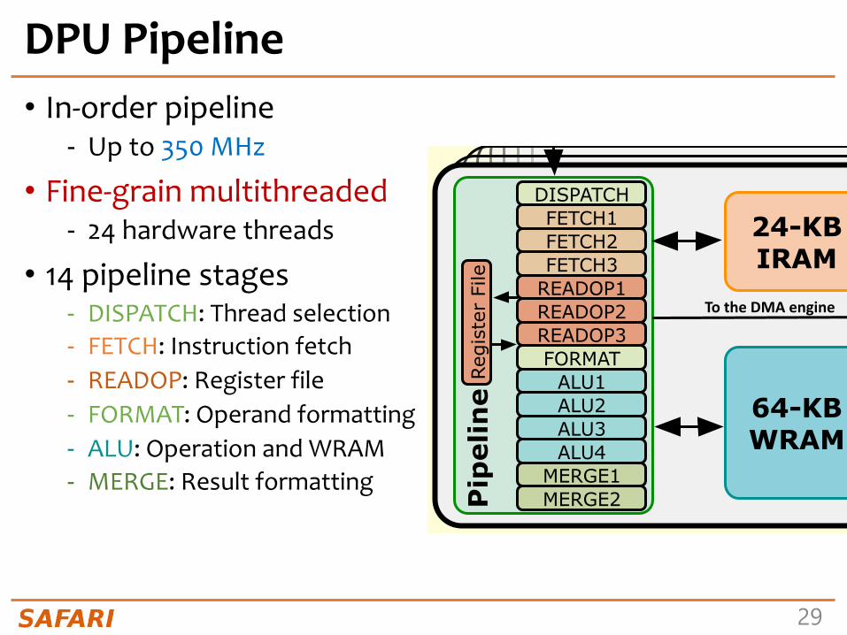
DPU Pipeline• In-order pipeline
- Up to 350 MHz
• Fine-grain multithreaded- 24 hardware threads
• 14 pipeline stages- DISPATCH: Thread selection- FETCH: Instruction fetch- READOP: Register file- FORMAT: Operand formatting- ALU: Operation and WRAM- MERGE: Result formatting
PIM Chip
24-KB IRAM
DM
A E
ng
ine
64-MB DRAM Bank
(MRAM)64-KB WRAM
x8
Control/Status Interface DDR4 Interface
DISPATCHFETCH1FETCH2FETCH3
READOP1READOP2READOP3FORMAT
ALU1ALU2ALU3ALU4
MERGE1MERGE2
Regi
ster
File
Pip
elin
e
64 bitsTo the DMA engine
30
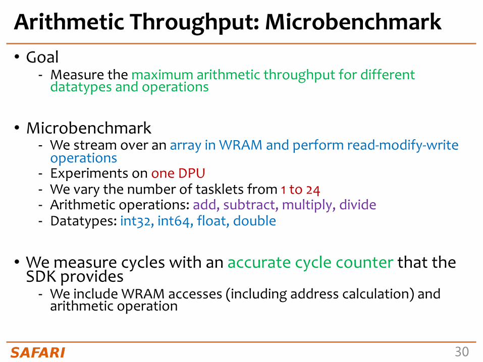
Arithmetic Throughput: Microbenchmark • Goal
- Measure the maximum arithmetic throughput for different datatypes and operations
• Microbenchmark- We stream over an array in WRAM and perform read-modify-write
operations- Experiments on one DPU- We vary the number of tasklets from 1 to 24- Arithmetic operations: add, subtract, multiply, divide- Datatypes: int32, int64, float, double
• We measure cycles with an accurate cycle counter that the SDK provides- We include WRAM accesses (including address calculation) and
arithmetic operation

31
Microbenchmark for INT32 ADD ThroughputC-
base
d co
deCo
mpi
led
code
(U
PMEM
DPU
ISA
)
1 #define SIZE 2562 int* bufferA = mem_alloc(SIZE * sizeof(int));3 for(int i = 0; i < SIZE; i++){4 int temp = bufferA[i];5 temp += scalar;6 bufferA[i] = temp;7 }
1 move r2, 02 .LBB0_1: // Loop header3 lsl_add r3, r0, r2, 2 // Address calculation4 lw r4, r3, 0 // Load from WRAM5 add r4, r4, r1 // Add6 sw r3, 0, r4 // Store to WRAM7 add r2, r2, 1 // Index update8 jneq r2, 256, .LBB0_1 // Conditional jump

32
0
1
2
3
4
5
6
1 3 5 7 9 11 13 15 17 19 21 23
Arith
met
ic T
hrou
ghpu
t (M
OPS
)
#Tasklets
(d) DOUBLE (1 DPU)
ADDSUBMULDIV
0
1
2
3
4
5
6
1 3 5 7 9 11 13 15 17 19 21 23
Arith
met
ic T
hrou
ghpu
t (M
OPS
)
#Tasklets
(c) FLOAT (1 DPU)
ADDSUBMULDIV
0
10
20
30
40
50
60
70
1 3 5 7 9 11 13 15 17 19 21 23
Arith
met
ic T
hrou
ghpu
t (M
OPS
)
#Tasklets
(b) INT64 (1 DPU)
ADDSUBMULDIV
0
10
20
30
40
50
60
70
1 3 5 7 9 11 13 15 17 19 21 23
Arith
met
ic T
hrou
ghpu
t (M
OPS
)
#Tasklets
(a) INT32 (1 DPU)
ADDSUBMULDIV
Arithmetic Throughput: 11 Tasklets
KEYOBSERVATION1ThearithmeticthroughputofaDRAMProcessingUnitsaturatesat11ormoretasklets.Thisobservationisconsistentfordifferentdatatypes(INT32,INT64,UINT32,UINT64,FLOAT,DOUBLE)andoperations(ADD,SUB,MUL,DIV).
33
0
1
2
3
4
5
6
1 3 5 7 9 11 13 15 17 19 21 23
Arith
met
ic T
hrou
ghpu
t (M
OPS
)
#Tasklets
(d) DOUBLE (1 DPU)
ADDSUBMULDIV
0
1
2
3
4
5
6
1 3 5 7 9 11 13 15 17 19 21 23
Arith
met
ic T
hrou
ghpu
t (M
OPS
)
#Tasklets
(c) FLOAT (1 DPU)
ADDSUBMULDIV
0
10
20
30
40
50
60
70
1 3 5 7 9 11 13 15 17 19 21 23
Arith
met
ic T
hrou
ghpu
t (M
OPS
)
#Tasklets
(b) INT64 (1 DPU)
ADDSUBMULDIV
0
10
20
30
40
50
60
70
1 3 5 7 9 11 13 15 17 19 21 23
Arith
met
ic T
hrou
ghpu
t (M
OPS
)
#Tasklets
(a) INT32 (1 DPU)
ADDSUBMULDIV
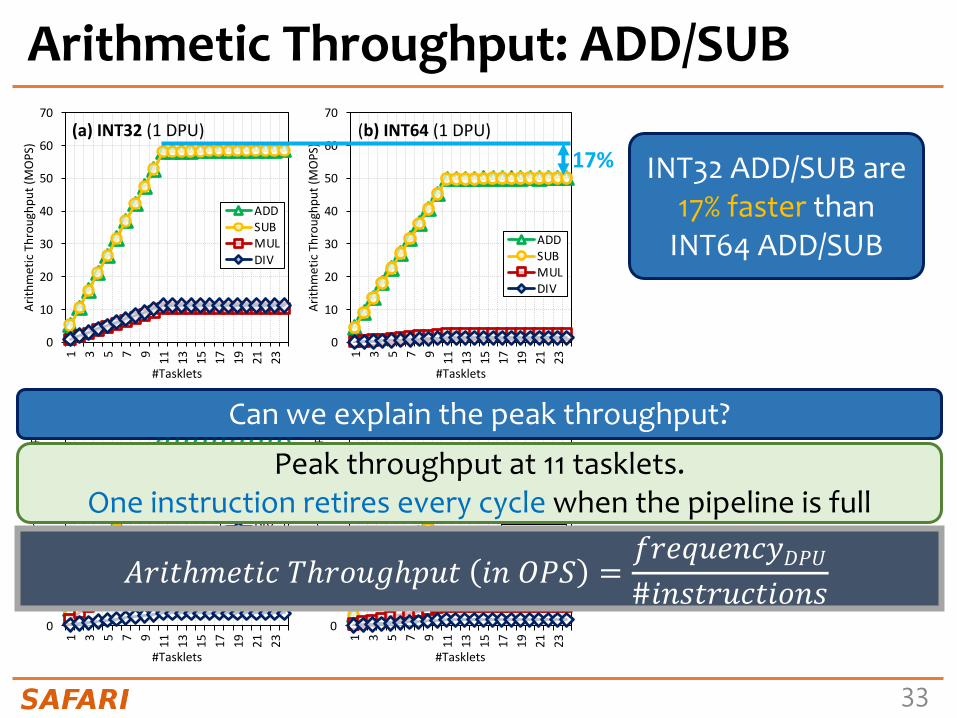
Arithmetic Throughput: ADD/SUB
INT32 ADD/SUB are 17% faster than
INT64 ADD/SUB
17%
Can we explain the peak throughput?
Peak throughput at 11 tasklets.One instruction retires every cycle when the pipeline is full
𝐴𝑟𝑖𝑡ℎ𝑚𝑒𝑡𝑖𝑐 𝑇ℎ𝑟𝑜𝑢𝑔ℎ𝑝𝑢𝑡 𝑖𝑛 𝑂𝑃𝑆 =𝑓𝑟𝑒𝑞𝑢𝑒𝑛𝑐𝑦𝐷𝑃𝑈#𝑖𝑛𝑠𝑡𝑟𝑢𝑐𝑡𝑖𝑜𝑛𝑠

34
Arithmetic Throughput: #Instructions• Compiler explorer: https://dpu.dev
6 instructions in the 32-bit ADD/SUB microbenchmark7 instructions in the 64-bit ADD/SUB microbenchmark

35
32-bit ADD/SUB: 6 instructions → 58.33 MOPS64-bit ADD/SUB: 7 instructions → 50.00 MOPS
at frequencyDPU = 350 MHz
0
10
20
30
40
50
60
70
1 3 5 7 9 11 13 15 17 19 21 23
Arith
met
ic T
hrou
ghpu
t (M
OPS
)
#Tasklets
(b) INT64 (1 DPU)
ADDSUBMULDIV
0
10
20
30
40
50
60
70
1 3 5 7 9 11 13 15 17 19 21 23
Arith
met
ic T
hrou
ghpu
t (M
OPS
)
#Tasklets
(a) INT32 (1 DPU)
ADDSUBMULDIV
Arithmetic Throughput: ADD/SUB
INT32 ADD/SUB are 17% faster than
INT64 ADD/SUB
17%
Can we explain the peak throughput?
Peak throughput at 11 tasklets.One instruction retires every cycle when the pipeline is full
𝐴𝑟𝑖𝑡ℎ𝑚𝑒𝑡𝑖𝑐 𝑇ℎ𝑟𝑜𝑢𝑔ℎ𝑝𝑢𝑡 𝑖𝑛 𝑂𝑃𝑆 =𝑓𝑟𝑒𝑞𝑢𝑒𝑛𝑐𝑦𝐷𝑃𝑈#𝑖𝑛𝑠𝑡𝑟𝑢𝑐𝑡𝑖𝑜𝑛𝑠

36
0
1
2
3
4
5
6
1 3 5 7 9 11 13 15 17 19 21 23
Arith
met
ic T
hrou
ghpu
t (M
OPS
)
#Tasklets
(d) DOUBLE (1 DPU)
ADDSUBMULDIV
0
1
2
3
4
5
6
1 3 5 7 9 11 13 15 17 19 21 23
Arith
met
ic T
hrou
ghpu
t (M
OPS
)
#Tasklets
(c) FLOAT (1 DPU)
ADDSUBMULDIV
0
10
20
30
40
50
60
70
1 3 5 7 9 11 13 15 17 19 21 23
Arith
met
ic T
hrou
ghpu
t (M
OPS
)
#Tasklets
(b) INT64 (1 DPU)
ADDSUBMULDIV
Arithmetic Throughput: MUL/DIV
0
10
20
30
40
50
60
70
1 3 5 7 9 11 13 15 17 19 21 23
Arith
met
ic T
hrou
ghpu
t (M
OPS
)
#Tasklets
(a) INT32 (1 DPU)
ADDSUBMULDIV
Huge throughput difference between
ADD/SUB and MUL/DIV
DPUs do not have a 32-bit multiplier
MUL/DIV implementation is based
on an instruction that performs bit shifting and
addition in 1 cycle(MUL/DIV take a maximum of 32
instructions)

37
0
1
2
3
4
5
6
1 3 5 7 9 11 13 15 17 19 21 23
Arith
met
ic T
hrou
ghpu
t (M
OPS
)
#Tasklets
(d) DOUBLE (1 DPU)
ADDSUBMULDIV
0
1
2
3
4
5
6
1 3 5 7 9 11 13 15 17 19 21 23
Arith
met
ic T
hrou
ghpu
t (M
OPS
)
#Tasklets
(c) FLOAT (1 DPU)
ADDSUBMULDIV
0
10
20
30
40
50
60
70
1 3 5 7 9 11 13 15 17 19 21 23
Arith
met
ic T
hrou
ghpu
t (M
OPS
)
#Tasklets
(b) INT64 (1 DPU)
ADDSUBMULDIV
0
10
20
30
40
50
60
70
1 3 5 7 9 11 13 15 17 19 21 23
Arith
met
ic T
hrou
ghpu
t (M
OPS
)
#Tasklets
(a) INT32 (1 DPU)
ADDSUBMULDIV
Arithmetic Throughput: Native SupportKEYOBSERVATION2• DPUsprovidenativehardwaresupportfor32-and64-bitintegeradditionandsubtraction,leadingtohighthroughputfortheseoperations.
• DPUsdonot nativelysupport32- and64-bitmultiplicationanddivision,andfloatingpointoperations.TheseoperationsareemulatedbytheUPMEMruntimelibrary,leadingtomuchlowerthroughput.

38
DPU: WRAM BandwidthPIM Chip
24-KB IRAM
DM
A E
ng
ine
64-MB DRAM Bank
(MRAM)64-KB WRAM
x8
Control/Status Interface DDR4 Interface
DISPATCHFETCH1FETCH2FETCH3
READOP1READOP2READOP3FORMAT
ALU1ALU2ALU3ALU4
MERGE1MERGE2
Regi
ster
File
Pip
elin
e
64 bits
64-KB WRAM
DISPATCHFETCH1FETCH2FETCH3
READOP1READOP2READOP3FORMAT
ALU1ALU2ALU3ALU4
MERGE1MERGE2
Regi
ster
File
Pip
elin
e

39
WRAM Bandwidth: Microbenchmark• Goal
- Measure the WRAM bandwidth for the STREAM benchmark
• Microbenchmark- We implement the four versions of STREAM: COPY, ADD,
SCALE, and TRIAD- The operations performed in ADD, SCALE, and TRIAD are
addition, multiplication, and addition+multiplication, respectively
- We vary the number of tasklets from 1 to 16- We show results for 1 DPU
• We do not include accesses to MRAM

40
STREAM Benchmark in WRAM8 bytes read, 8 bytes written,
no arithmetic operations
16 bytes read, 8 bytes written, ADD
8 bytes read, 8 bytes written, MUL
16 bytes read, 8 bytes written, MUL, ADD
// COPYfor(int i = 0; i < SIZE; i++){
bufferB[i] = bufferA[i];}
// ADDfor(int i = 0; i < SIZE; i++){
bufferC[i] = bufferA[i] + bufferB[i];}
// SCALEfor(int i = 0; i < SIZE; i++){
bufferB[i] = scalar * bufferA[i];}
// TRIADfor(int i = 0; i < SIZE; i++){
bufferC[i] = bufferA[i] + scalar * bufferB[i];}
41
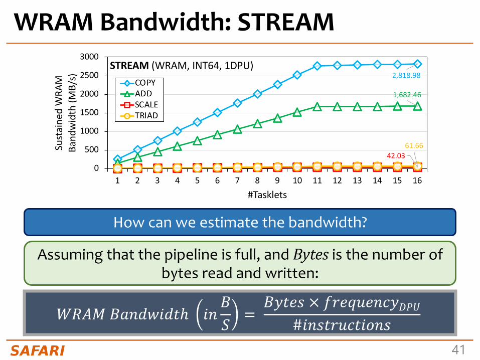
WRAM Bandwidth: STREAM
How can we estimate the bandwidth?
𝑊𝑅𝐴𝑀 𝐵𝑎𝑛𝑑𝑤𝑖𝑑𝑡ℎ 𝑖𝑛𝐵𝑆
=𝐵𝑦𝑡𝑒𝑠 × 𝑓𝑟𝑒𝑞𝑢𝑒𝑛𝑐𝑦𝐷𝑃𝑈
#𝑖𝑛𝑠𝑡𝑟𝑢𝑐𝑡𝑖𝑜𝑛𝑠
2,818.98
1,682.46
42.0361.66
0
500
1000
1500
2000
2500
3000
1 2 3 4 5 6 7 8 9 10 11 12 13 14 15 16
Sust
aine
d W
RAM
Ba
ndw
idth
(MB/
s)
#Tasklets
STREAM (WRAM, INT64, 1DPU)COPYADDSCALETRIAD
Assuming that the pipeline is full, and Bytes is the number of bytes read and written:

42
𝑊𝑅𝐴𝑀 𝐵𝑎𝑛𝑑𝑤𝑖𝑑𝑡ℎ 𝑖𝑛𝐵𝑆
=𝐵𝑦𝑡𝑒𝑠 × 𝑓𝑟𝑒𝑞𝑢𝑒𝑛𝑐𝑦𝐷𝑃𝑈
#𝑖𝑛𝑠𝑡𝑟𝑢𝑐𝑡𝑖𝑜𝑛𝑠𝑊𝑅𝐴𝑀 𝐵𝑎𝑛𝑑𝑤𝑖𝑑𝑡ℎ 𝑖𝑛𝐵𝑆
= 2,800𝑀𝐵𝑠𝑎𝑡 350 𝑀𝐻𝑧
WRAM Bandwidth: COPY
2,818.98
1,682.46
42.0361.66
0
500
1000
1500
2000
2500
3000
1 2 3 4 5 6 7 8 9 10 11 12 13 14 15 16
Sust
aine
d W
RAM
Ba
ndw
idth
(MB/
s)
#Tasklets
STREAM (WRAM, INT64, 1DPU)COPYADDSCALETRIAD
COPY executes 2 instructions (WRAM load and store).With 11 tasklets, 11 × 16 bytes in 22 cycles:
43
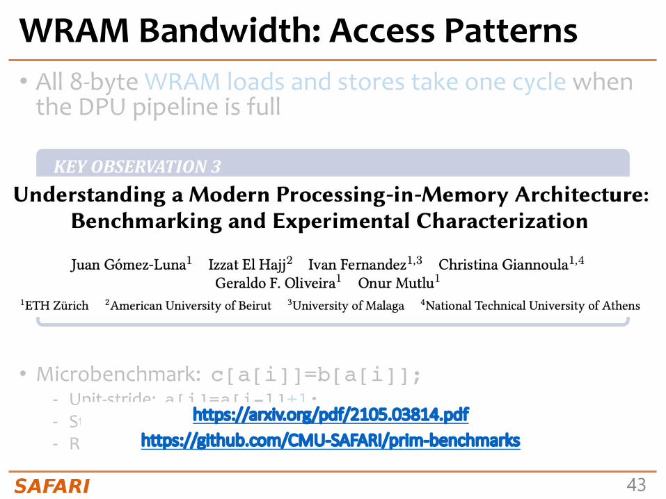
WRAM Bandwidth: Access Patterns• All 8-byte WRAM loads and stores take one cycle when
the DPU pipeline is full
• Microbenchmark: c[a[i]]=b[a[i]];- Unit-stride: a[i]=a[i-1]+1;- Strided: a[i]=a[i-1]+stride;- Random: a[i]=rand();
KEYOBSERVATION3ThesustainedbandwidthprovidedbytheDPU’sinternalWorkingmemory(WRAM)isindependentofthememoryaccesspattern(eitherstreaming,strided,orrandomaccesspattern).
All8-byteWRAMloadsandstorestakeonecycle,whentheDPU’spipelineisfull(i.e.,with11ormoretasklets).
https://arxiv.org/pdf/2105.03814.pdfhttps://github.com/CMU-SAFARI/prim-benchmarks
44
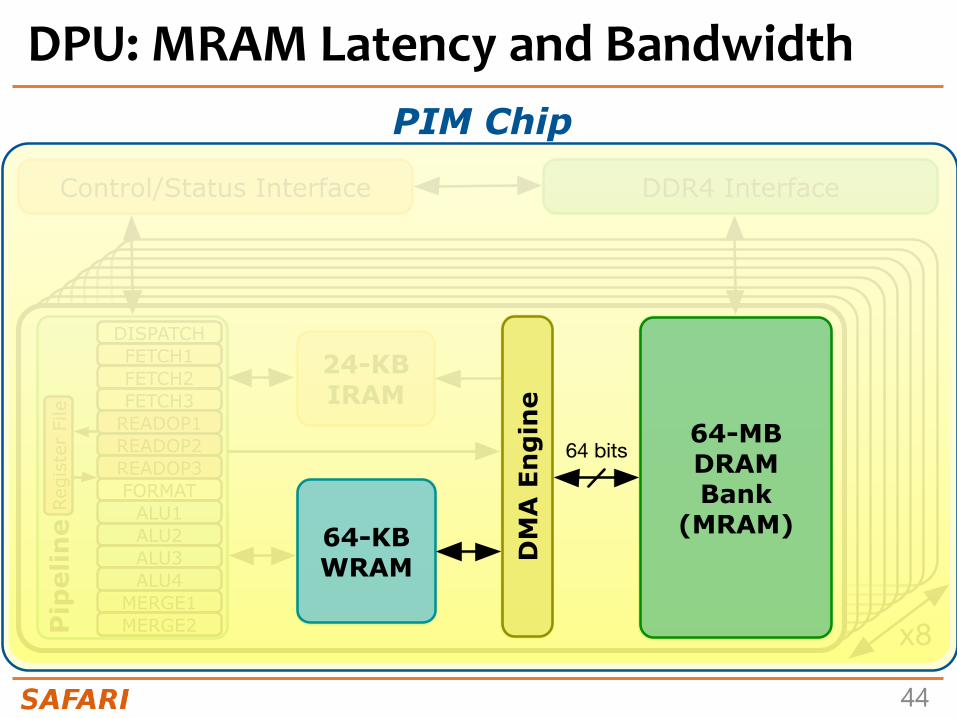
DPU: MRAM Latency and BandwidthPIM Chip
24-KB IRAM
DM
A E
ng
ine
64-MB DRAM Bank
(MRAM)64-KB WRAM
x8
Control/Status Interface DDR4 Interface
DISPATCHFETCH1FETCH2FETCH3
READOP1READOP2READOP3FORMAT
ALU1ALU2ALU3ALU4
MERGE1MERGE2
Regi
ster
File
Pip
elin
e
64 bits
DM
A E
ng
ine
64-MB DRAM Bank
(MRAM)64-KB WRAM
64 bits

45
MRAM Bandwidth• Goal
- Measure MRAM bandwidth for different access patterns
• Microbenchmarks- Latency of a single DMA transfer for different transfer sizes
• mram_read(); // MRAM-WRAM DMA transfer• mram_write(); // WRAM-MRAM DMA transfer
- STREAM benchmark• COPY, COPY-DMA• ADD, SCALE, TRIAD
- Strided access pattern• Coarse-grain strided access• Fine-grain strided access
- Random access pattern (GUPS)
• We do include accesses to MRAM
46
MRAM Read and Write Latency (I)
𝑀𝑅𝐴𝑀 𝐵𝑎𝑛𝑑𝑤𝑖𝑑𝑡ℎ 𝑖𝑛𝐵𝑆
=𝑠𝑖𝑧𝑒 × 𝑓𝑟𝑒𝑞𝑢𝑒𝑛𝑐𝑦𝐷𝑃𝑈𝑀𝑅𝐴𝑀 𝐿𝑎𝑡𝑒𝑛𝑐𝑦
We can model the MRAM latency with a linear expression
𝑀𝑅𝐴𝑀 𝐿𝑎𝑡𝑒𝑛𝑐𝑦 𝑖𝑛 𝑐𝑦𝑐𝑙𝑒𝑠 = 𝛼 + 𝛽×𝑠𝑖𝑧𝑒
628.23
32
128
512
2048
1
10
100
10008 16 32 64 128
256
512
1024
2048
Late
ncy
(cyc
les)
Band
wid
th (M
B/s)
Data transfer size (bytes)
MRAM Read633.22
32
128
512
2048
1
10
100
1000
8 16 32 64 128
256
512
1024
2048
Late
ncy
(cyc
les)
Band
wid
th (M
B/s)
Data transfer size (bytes)
MRAM Write
In our measurements, 𝛽 equals 0.5 cycles/byte.Theoretical maximum MRAM bandwidth = 700 MB/s at 350 MHz

47
𝑀𝑅𝐴𝑀 𝐿𝑎𝑡𝑒𝑛𝑐𝑦 𝑖𝑛 𝑐𝑦𝑐𝑙𝑒𝑠 = 𝛼 + 𝛽×𝑠𝑖𝑧𝑒
KEYOBSERVATION4
• TheDPU’sMainmemory(MRAM)bankaccesslatencyincreaseslinearlywiththetransfersize.• ThemaximumtheoreticalMRAMbandwidthis2bytespercycle.
MRAM Read and Write Latency (II)628.23
32
128
512
2048
1
10
100
10008 16 32 64 128
256
512
1024
2048
Late
ncy
(cyc
les)
Band
wid
th (M
B/s)
Data transfer size (bytes)
MRAM Read633.22
32
128
512
2048
1
10
100
1000
8 16 32 64 128
256
512
1024
2048
Late
ncy
(cyc
les)
Band
wid
th (M
B/s)
Data transfer size (bytes)
MRAM Write
48
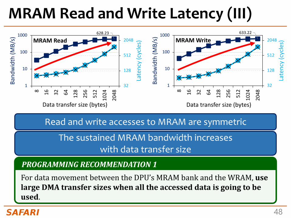
MRAM Read and Write Latency (III)
Read and write accesses to MRAM are symmetric
628.23
32
128
512
2048
1
10
100
10008 16 32 64 128
256
512
1024
2048
Late
ncy
(cyc
les)
Band
wid
th (M
B/s)
Data transfer size (bytes)
MRAM Read633.22
32
128
512
2048
1
10
100
1000
8 16 32 64 128
256
512
1024
2048
Late
ncy
(cyc
les)
Band
wid
th (M
B/s)
Data transfer size (bytes)
MRAM Write
The sustained MRAM bandwidth increases with data transfer size
PROGRAMMINGRECOMMENDATION1FordatamovementbetweentheDPU’sMRAMbankandtheWRAM,uselargeDMAtransfersizeswhenalltheaccesseddataisgoingtobeused.

49
MRAM Read and Write Latency (IV)628.23
32
128
512
2048
1
10
100
10008 16 32 64 128
256
512
1024
2048
Late
ncy
(cyc
les)
Band
wid
th (M
B/s)
Data transfer size (bytes)
MRAM Read633.22
32
128
512
2048
1
10
100
1000
8 16 32 64 128
256
512
1024
2048
Late
ncy
(cyc
les)
Band
wid
th (M
B/s)
Data transfer size (bytes)
MRAM Write
PROGRAMMINGRECOMMENDATION2ForsmalltransfersbetweentheMRAMbankandtheWRAM,fetchmorebytesthannecessarywithina128-bytelimit.DoingsoincreasesthelikelihoodoffindingdatainWRAMforlateraccesses(i.e.,theprogramcancheckwhetherthedesireddataisinWRAMbeforeissuinganewMRAMaccess).
PROGRAMMINGRECOMMENDATION3ChoosethedatatransfersizebetweentheMRAMbankandtheWRAMbasedontheprogram’sWRAMusage,asitimposesatradeoffbetweenthesustainedMRAMbandwidthandthenumberoftasklets thatcanrunintheDPU(whichisdictatedbythelimitedWRAMcapacity).
https://arxiv.org/pdf/2105.03814.pdfhttps://github.com/CMU-SAFARI/prim-benchmarks

50
MRAM Bandwidth• Goal
- Measure MRAM bandwidth for different access patterns
• Microbenchmarks- Latency of a single DMA transfer for different transfer sizes
• mram_read(); // MRAM-WRAM DMA transfer• mram_write(); // WRAM-MRAM DMA transfer
- STREAM benchmark• COPY, COPY-DMA• ADD, SCALE, TRIAD
- Strided access pattern• Coarse-grain strided access• Fine-grain strided access
- Random access pattern (GUPS)
• We do include accesses to MRAM

51
STREAM Benchmark in MRAM// COPY// Load current MRAM block to WRAMmram_read((__mram_ptr void const*)mram_address_A, bufferA,
SIZE * sizeof(uint64_t));
for(int i = 0; i < SIZE; i++){bufferB[i] = bufferA[i];
}
// Write WRAM block to MRAMmram_write(bufferB, (__mram_ptr void*)mram_address_B,
SIZE * sizeof(uint64_t));
// COPY-DMA// Load current MRAM block to WRAMmram_read((__mram_ptr void const*)mram_address_A, bufferA,
SIZE * sizeof(uint64_t));
// Write WRAM block to MRAMmram_write(bufferB, (__mram_ptr void*)mram_address_B,
SIZE * sizeof(uint64_t));
52
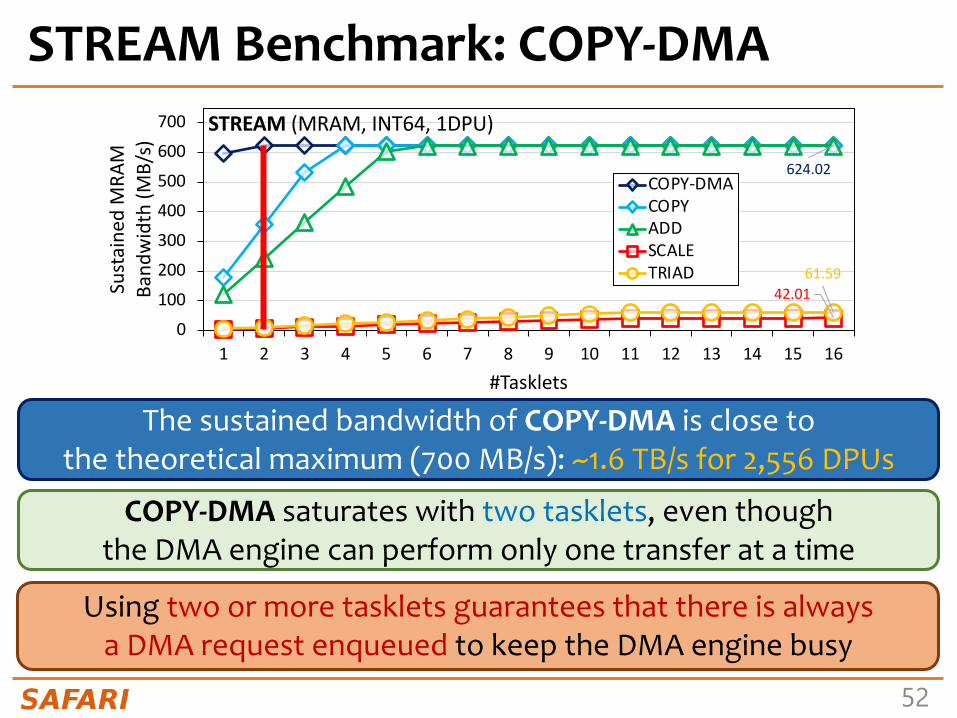
STREAM Benchmark: COPY-DMA
624.02
42.0161.59
0
100
200
300
400
500
600
700
1 2 3 4 5 6 7 8 9 10 11 12 13 14 15 16
Sust
aine
d M
RAM
Ba
ndw
idth
(MB/
s)
#Tasklets
STREAM (MRAM, INT64, 1DPU)
COPY-DMACOPYADDSCALETRIAD
The sustained bandwidth of COPY-DMA is close to the theoretical maximum (700 MB/s): ~1.6 TB/s for 2,556 DPUs
COPY-DMA saturates with two tasklets, even though the DMA engine can perform only one transfer at a time
Using two or more tasklets guarantees that there is always a DMA request enqueued to keep the DMA engine busy

53
STREAM Benchmark: Bandwidth Saturation (I)
624.02
42.0161.59
0
100
200
300
400
500
600
700
1 2 3 4 5 6 7 8 9 10 11 12 13 14 15 16
Sust
aine
d M
RAM
Ba
ndw
idth
(MB/
s)
#Tasklets
STREAM (MRAM, INT64, 1DPU)
COPY-DMACOPYADDSCALETRIAD
COPY and ADD saturate at 4 and 6 tasklets, respectively
SCALE and TRIAD saturate at 11 tasklets
The latency of MRAM accesses becomes longer than the pipeline latency after 4 and 6 tasklets for COPY and ADD, respectively
The pipeline latency of SCALE and TRIAD is longer than the MRAM latency for any number of tasklets (both use costly MUL)

54
STREAM Benchmark: Bandwidth Saturation (II)
624.02
42.0161.59
0
100
200
300
400
500
600
700
1 2 3 4 5 6 7 8 9 10 11 12 13 14 15 16
Sust
aine
d M
RAM
Ba
ndw
idth
(MB/
s)
#Tasklets
STREAM (MRAM, INT64, 1DPU)
COPY-DMACOPYADDSCALETRIAD
KEYOBSERVATION5• WhentheaccesslatencytoanMRAMbankforastreamingbenchmark(COPY-DMA,COPY,ADD)islargerthanthepipelinelatency(i.e.,executionlatencyofarithmeticoperationsandWRAMaccesses),theperformanceoftheDPUsaturatesatanumberoftasklets smallerthan11.Thisisamemory-boundworkload.• Whenthepipelinelatency forastreamingbenchmark(SCALE,TRIAD)islargerthantheMRAMaccesslatency,theperformanceofaDPUsaturatesat11tasklets.Thisisacompute-boundworkload.

55
MRAM Bandwidth• Goal
- Measure MRAM bandwidth for different access patterns
• Microbenchmarks- Latency of a single DMA transfer for different transfer sizes
• mram_read(); // MRAM-WRAM DMA transfer• mram_write(); // WRAM-MRAM DMA transfer
- STREAM benchmark• COPY, COPY-DMA• ADD, SCALE, TRIAD
- Strided access pattern• Coarse-grain strided access• Fine-grain strided access
- Random access pattern (GUPS)
• We do include accesses to MRAM

56
Strided and Random Access to MRAM// COARSE-GRAINED STRIDED ACCESS// Load current MRAM block to WRAMmram_read((__mram_ptr void const*)mram_address_A, bufferA,
SIZE * sizeof(uint64_t));mram_read((__mram_ptr void const*)mram_address_B, bufferB,
SIZE * sizeof(uint64_t));
for(int i = 0; i < SIZE; i += stride){bufferB[i] = bufferA[i];
}// Write WRAM block to MRAMmram_write(bufferB, (__mram_ptr void*)mram_address_B,
SIZE * sizeof(uint64_t));
// FINE-GRAINED STRIDED & RANDOM ACCESSfor(int i = 0; i < SIZE; i += stride){
int index = i * sizeof(uint64_t);// Load current MRAM element to WRAMmram_read((__mram_ptr void const*)(mram_address_A + index), bufferA,
sizeof(uint64_t));
// Write WRAM element to MRAMmram_write(bufferA, (__mram_ptr void*)(mram_address_B + index),
sizeof(uint64_t));}

57
Strided and Random Accesses (I)622.36
77.86
0
100
200
300
400
500
600
7001 2 4 8 16 32 64 128
256
512
1024
2048
4096
Sust
aine
d M
RAM
Ban
dwid
th
(MB/
s)
Stride
(a) Coarse-grained Strided (MRAM, 1 DPU)
Coarse-grained DMA - 1 taskletCoarse-grained DMA - 2 taskletsCoarse-grained DMA - 4 taskletsCoarse-grained DMA - 8 taskletsCoarse-grained DMA - 16 tasklets
72.58
0
10
20
30
40
50
60
70
80
90
1 2 4 8 16 32 64 128
256
512
1024
2048
4096
GUPS
Sust
aine
d M
RAM
Ban
dwid
th
(MB/
s)
Stride
(b) Fine-grained Strided & Random (MRAM, 1 DPU)
Fine-grained DMA - 1 taskletFine-grained DMA - 2 taskletsFine-grained DMA - 4 taskletsFine-grained DMA - 8 taskletsFine-grained DMA - 16 tasklets
Rand
om(G
UPS
)
Large difference in maximum sustained bandwidth between coarse-grained and fine-grained DMA
Coarse-grained DMA uses 1,024-byte transfers, while fine-grained DMA uses 8-byte transfers
Random access achieves very similar maximum sustained bandwidth to fine-grained strided approach

58
Strided and Random Accesses (II)622.36
77.86
0
100
200
300
400
500
600
7001 2 4 8 16 32 64 128
256
512
1024
2048
4096
Sust
aine
d M
RAM
Ban
dwid
th
(MB/
s)
Stride
(a) Coarse-grained Strided (MRAM, 1 DPU)
Coarse-grained DMA - 1 taskletCoarse-grained DMA - 2 taskletsCoarse-grained DMA - 4 taskletsCoarse-grained DMA - 8 taskletsCoarse-grained DMA - 16 tasklets
72.58
0
10
20
30
40
50
60
70
80
90
1 2 4 8 16 32 64 128
256
512
1024
2048
4096
GUPS
Sust
aine
d M
RAM
Ban
dwid
th
(MB/
s)
Stride
(b) Fine-grained Strided & Random (MRAM, 1 DPU)
Fine-grained DMA - 1 taskletFine-grained DMA - 2 taskletsFine-grained DMA - 4 taskletsFine-grained DMA - 8 taskletsFine-grained DMA - 16 tasklets
Rand
om(G
UPS
)
The sustained MRAM bandwidth of coarse-grained DMA decreases as the stride increases
The effective utilization of the transferred data decreases as the stride becomes larger (e.g., a stride 4 means that only one
fourth of the transferred data is used)

59
Strided and Random Accesses (III)622.36
77.86
0
100
200
300
400
500
600
7001 2 4 8 16 32 64 128
256
512
1024
2048
4096
Sust
aine
d M
RAM
Ban
dwid
th
(MB/
s)
Stride
(a) Coarse-grained Strided (MRAM, 1 DPU)
Coarse-grained DMA - 1 taskletCoarse-grained DMA - 2 taskletsCoarse-grained DMA - 4 taskletsCoarse-grained DMA - 8 taskletsCoarse-grained DMA - 16 tasklets
72.58
0
10
20
30
40
50
60
70
80
90
1 2 4 8 16 32 64 128
256
512
1024
2048
4096
GUPS
Sust
aine
d M
RAM
Ban
dwid
th
(MB/
s)
Stride
(b) Fine-grained Strided & Random (MRAM, 1 DPU)
Fine-grained DMA - 1 taskletFine-grained DMA - 2 taskletsFine-grained DMA - 4 taskletsFine-grained DMA - 8 taskletsFine-grained DMA - 16 tasklets
Rand
om(G
UPS
)
For a stride of 16 or larger, the fine-grained DMA approach achieves higher bandwidth
With stride 16, only one sixteenth of the maximum sustained bandwidth (622.36 MB/s) of coarse-grained DMA
is effectively used, which is lower than the bandwidth of fine-grained DMA (72.58 MB/s)

60
Strided and Random Accesses (IV)622.36
77.86
0
100
200
300
400
500
600
7001 2 4 8 16 32 64 128
256
512
1024
2048
4096
Sust
aine
d M
RAM
Ban
dwid
th
(MB/
s)
Stride
(a) Coarse-grained Strided (MRAM, 1 DPU)
Coarse-grained DMA - 1 taskletCoarse-grained DMA - 2 taskletsCoarse-grained DMA - 4 taskletsCoarse-grained DMA - 8 taskletsCoarse-grained DMA - 16 tasklets
72.58
0
10
20
30
40
50
60
70
80
90
1 2 4 8 16 32 64 128
256
512
1024
2048
4096
GUPS
Sust
aine
d M
RAM
Ban
dwid
th
(MB/
s)
Stride
(b) Fine-grained Strided & Random (MRAM, 1 DPU)
Fine-grained DMA - 1 taskletFine-grained DMA - 2 taskletsFine-grained DMA - 4 taskletsFine-grained DMA - 8 taskletsFine-grained DMA - 16 tasklets
Rand
om(G
UPS
)
PROGRAMMINGRECOMMENDATION4• Forstrided accesspatternswithastridesmallerthan168-byteelements,fetchalargecontiguouschunk (e.g.,1,024bytes)fromaDPU’sMRAMbank.• Forstrided accesspatternswithlargerstridesandrandomaccesspatterns,fetchonlythedataelementsthatareneededfromanMRAMbank.
61
DPU: Arithmetic Throughput vs. Operational Intensity
PIM Chip
24-KB IRAM
DM
A E
ng
ine
64-MB DRAM Bank
(MRAM)64-KB WRAM
x8
Control/Status Interface DDR4 Interface
DISPATCHFETCH1FETCH2FETCH3
READOP1READOP2READOP3FORMAT
ALU1ALU2ALU3ALU4
MERGE1MERGE2
Regi
ster
File
Pip
elin
e
64 bits
DM
A E
ng
ine
64-MB DRAM Bank
(MRAM)64-KB WRAM
DISPATCHFETCH1FETCH2FETCH3
READOP1READOP2READOP3FORMAT
ALU1ALU2ALU3ALU4
MERGE1MERGE2
Regi
ster
File
Pip
elin
e
64 bits

62
Arithmetic Throughput vs. Operational Intensity (I)
• Goal- Characterize memory-bound regions and compute-bound regions for
different datatypes and operations
• Microbenchmark- We load one chunk of an MRAM array into WRAM- Perform a variable number of operations on the data- Write back to MRAM
• The experiment is inspired by the Roofline model*
• We define operational intensity (OI) as the number of arithmetic operations performed per byte accessed from MRAM (OP/B)
• The pipeline latency changes with the operational intensity, but the MRAM access latency is fixed
*S. Williams et al., “Roofline: An Insightful Visual Performance Model for Multi-core Architectures,” CACM, 2009

63
Arithmetic Throughput vs. Operational Intensity (II)
int repetitions = input_repeat >= 1.0 ? (int)input_repeat : 1;int stride = input_repeat >= 1.0 ? 1 : (int)(1 / input_repeat);
// Load current MRAM block to WRAMmram_read((__mram_ptr void const*)mram_address_A, bufferA, SIZE * sizeof(T));
// Updatefor(int r = 0; r < repetitions; r++){
for(int i = 0; i < SIZE; i+=stride){#ifdef ADD
bufferA[i] += scalar; // ADD #elif SUB
bufferA[i] -= scalar; // SUB#elif MUL
bufferA[i] *= scalar; // MUL #elif DIV
bufferA[i] /= scalar; // DIV#endif
}}
// Write WRAM block to MRAMmram_write(bufferA, (__mram_ptr void*)mram_address_B, SIZE * sizeof(T));
input_repeat greater or equal to 1 indicates the (integer)
number of repetitions per input element
input_repeat smaller than 1 indicates the fraction of elements
that are updated

64
Arithmetic Throughput vs. Operational Intensity (III)
1234567891011121314151612345678910111213141516
1234567891011121314151612345678910111213141516 1
2345678910111213141516 12345678910111213141516
12345678910111213141516
12345678910111213141516
12345678910111213141516
123456789
10111213141516
123456789
10111213141516
123456789
10111213141516
123456789
10111213141516
123456789
10111213141516
123456789
10111213141516
0.030.060.130.250.501.002.004.008.00
16.0032.0064.00
1/4096
1/2048
1/1024
1/512
1/256
1/128
1/64
1/32
1/16
1/8
1/4
1/2
1 2 4 8
Arith
met
ic T
hrou
ghpu
t (M
OPS
, log
scal
e)
Operational Intensity (OP/B)
(a) INT32, ADD (1 DPU)
12345678910111213141516
12345678910111213141516 1
2345678910111213141516 12345678910111213141516
12345678910111213141516
12345678910111213141516
123456789
10111213141516
123456789
10111213141516
123456789
10111213141516
123456789
10111213141516
123456789
10111213141516
123456789
10111213141516
123456789
10111213141516
123456789
10111213141516
123456789
10111213141516
0.030.060.130.250.501.002.004.008.00
16.0032.0064.00
1/4096
1/2048
1/1024
1/512
1/256
1/128
1/64
1/32
1/16
1/8
1/4
1/2
1 2 4 8
Arith
met
ic T
hrou
ghpu
t (M
OPS
, log
scal
e)
Operational Intensity (OP/B)
(b) INT32, MUL (1 DPU)
12345678910111213141516 1
2345678910111213141516 12345678910111213141516
12345678910111213141516
12345678910111213141516
123456789
10111213141516
123456789
10111213141516
123456789
10111213141516
123456789
10111213141516
123456789
10111213141516
123456789
10111213141516
123456789
10111213141516
123456789
10111213141516
123456789
10111213141516
123456789
10111213141516
0.030.060.130.250.501.002.004.008.00
16.0032.0064.00
1/4096
1/2048
1/1024
1/512
1/256
1/128
1/64
1/32
1/16
1/8
1/4
1/2
1 2 4 8
Arith
met
ic T
hrou
ghpu
t (M
OPS
, log
scal
e)
Operational Intensity (OP/B)
(c) FLOAT, ADD (1 DPU)
12345678910111213141516
12345678910111213141516
12345678910111213141516
12345678910111213141516
123456789
10111213141516
123456789
10111213141516
123456789
10111213141516
123456789
10111213141516
123456789
10111213141516
123456789
10111213141516
123456789
10111213141516
123456789
10111213141516
123456789
10111213141516
123456789
10111213141516
123456789
10111213141516
0.030.060.130.250.501.002.004.008.00
16.0032.0064.00
1/4096
1/2048
1/1024
1/512
1/256
1/128
1/64
1/32
1/16
1/8
1/4
1/2
1 2 4 8
Arith
met
ic T
hrou
ghpu
t (M
OPS
, log
scal
e)
Operational Intensity (OP/B)
(d) FLOAT, MUL (1 DPU)
21 8421 84
21 84 21 84
We show results of arithmetic throughput vs. operational intensity for (a) 32-bit integer ADD, (b) 32-bit integer MUL,
(c) 32-bit floating-point ADD, and (d) 32-bit floating-point MUL (results for other datatypes and operations show similar trends)

65
Arithmetic Throughput vs. Operational Intensity (IV)
1234567891011121314151612345678910111213141516
1234567891011121314151612345678910111213141516 1
2345678910111213141516 12345678910111213141516
12345678910111213141516
12345678910111213141516
12345678910111213141516
123456789
10111213141516
123456789
10111213141516
123456789
10111213141516
123456789
10111213141516
123456789
10111213141516
123456789
10111213141516
0.030.060.130.250.501.002.004.008.00
16.0032.0064.00
1/4
096
1/2
048
1/1
024
1/5
12
1/2
56
1/1
28
1/6
4
1/3
2
1/1
6
1/8
1/4
1/21 2 4 8
Arith
met
ic T
hrou
ghpu
t (M
OPS
, log
scal
e)
Operational Intensity (OP/B)
(a) INT32, ADD (1 DPU)
21 84
Memory-bound region
Compute-bound region
In the memory-bound region, the arithmetic
throughput increases with the operational intensity
In the compute-bound region, the arithmetic
throughput is flat at its maximum
The throughput saturation point is the operational intensity where the transition between
the memory-bound region and the compute-bound region happens
The throughput saturation point is as low as ¼ OP/B, i.e., 1 integer addition per every 32-bit element fetched

66
Arithmetic Throughput vs. Operational Intensity (V)
1234567891011121314151612345678910111213141516
1234567891011121314151612345678910111213141516 1
2345678910111213141516 12345678910111213141516
12345678910111213141516
12345678910111213141516
12345678910111213141516
123456789
10111213141516
123456789
10111213141516
123456789
10111213141516
123456789
10111213141516
123456789
10111213141516
123456789
10111213141516
0.030.060.130.250.501.002.004.008.00
16.0032.0064.00
1/4096
1/2048
1/1024
1/512
1/256
1/128
1/64
1/32
1/16
1/8
1/4
1/2
1 2 4 8
Arith
met
ic T
hrou
ghpu
t (M
OPS
, log
scal
e)
Operational Intensity (OP/B)
(a) INT32, ADD (1 DPU)
12345678910111213141516
12345678910111213141516 1
2345678910111213141516 12345678910111213141516
12345678910111213141516
12345678910111213141516
123456789
10111213141516
123456789
10111213141516
123456789
10111213141516
123456789
10111213141516
123456789
10111213141516
123456789
10111213141516
123456789
10111213141516
123456789
10111213141516
123456789
10111213141516
0.030.060.130.250.501.002.004.008.00
16.0032.0064.00
1/4096
1/2048
1/1024
1/512
1/256
1/128
1/64
1/32
1/16
1/8
1/4
1/2
1 2 4 8
Arith
met
ic T
hrou
ghpu
t (M
OPS
, log
scal
e)
Operational Intensity (OP/B)
(b) INT32, MUL (1 DPU)
12345678910111213141516 1
2345678910111213141516 12345678910111213141516
12345678910111213141516
12345678910111213141516
123456789
10111213141516
123456789
10111213141516
123456789
10111213141516
123456789
10111213141516
123456789
10111213141516
123456789
10111213141516
123456789
10111213141516
123456789
10111213141516
123456789
10111213141516
123456789
10111213141516
0.030.060.130.250.501.002.004.008.00
16.0032.0064.00
1/4096
1/2048
1/1024
1/512
1/256
1/128
1/64
1/32
1/16
1/8
1/4
1/2
1 2 4 8
Arith
met
ic T
hrou
ghpu
t (M
OPS
, log
scal
e)
Operational Intensity (OP/B)
(c) FLOAT, ADD (1 DPU)
12345678910111213141516
12345678910111213141516
12345678910111213141516
12345678910111213141516
123456789
10111213141516
123456789
10111213141516
123456789
10111213141516
123456789
10111213141516
123456789
10111213141516
123456789
10111213141516
123456789
10111213141516
123456789
10111213141516
123456789
10111213141516
123456789
10111213141516
123456789
10111213141516
0.030.060.130.250.501.002.004.008.00
16.0032.0064.00
1/4096
1/2048
1/1024
1/512
1/256
1/128
1/64
1/32
1/16
1/8
1/4
1/2
1 2 4 8
Arith
met
ic T
hrou
ghpu
t (M
OPS
, log
scal
e)
Operational Intensity (OP/B)
(d) FLOAT, MUL (1 DPU)
21 8421 84
21 84 21 84KEYOBSERVATION6ThearithmeticthroughputofaDRAMProcessingUnit(DPU)saturatesatloworverylowoperationalintensity (e.g.,1integeradditionper32-bitelement).Thus,theDPUisfundamentallyacompute-boundprocessor.Weexpectmostreal-worldworkloadsbecompute-boundintheUPMEMPIMarchitecture.

67
Outline• Introduction
- Accelerator Model- UPMEM-based PIM System Overview
• UPMEM PIM Programming- Vector Addition- CPU-DPU Data Transfers- Inter-DPU Communication- CPU-DPU/DPU-CPU Transfer Bandwidth
• DRAM Processing Unit- Arithmetic Throughput- WRAM and MRAM Bandwidth
• PrIM Benchmarks- Roofline Model- Benchmark Diversity
• Evaluation- Strong and Weak Scaling- Comparison to CPU and GPU
• Key Takeaways
68
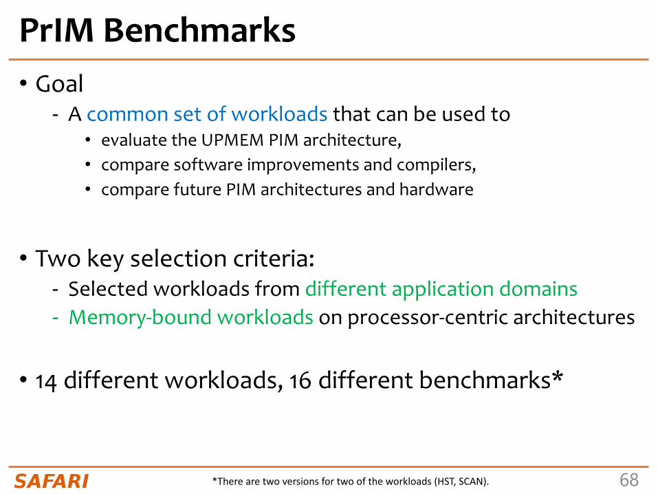
PrIM Benchmarks• Goal
- A common set of workloads that can be used to • evaluate the UPMEM PIM architecture,• compare software improvements and compilers,• compare future PIM architectures and hardware
• Two key selection criteria:- Selected workloads from different application domains- Memory-bound workloads on processor-centric architectures
• 14 different workloads, 16 different benchmarks*
*There are two versions for two of the workloads (HST, SCAN).
69
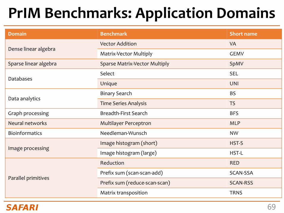
PrIM Benchmarks: Application DomainsDomain Benchmark Short name
Dense linear algebraVector Addition VA
Matrix-Vector Multiply GEMV
Sparse linear algebra Sparse Matrix-Vector Multiply SpMV
DatabasesSelect SEL
Unique UNI
Data analyticsBinary Search BS
Time Series Analysis TS
Graph processing Breadth-First Search BFS
Neural networks Multilayer Perceptron MLP
Bioinformatics Needleman-Wunsch NW
Image processingImage histogram (short) HST-S
Image histogram (large) HST-L
Parallel primitives
Reduction RED
Prefix sum (scan-scan-add) SCAN-SSA
Prefix sum (reduce-scan-scan) SCAN-RSS
Matrix transposition TRNS

70
BFS
BS
GEMVMLP
SELSpMV
TS UNI
VA
HST
REDSCAN
NWTRNS
0.125
0.25
0.5
1
2
4
8
16
0.01 0.1 1 10
Perf
orm
ance
(GO
PS)
Arithmetic Intensity (OP/B)
Peak compute performance
Roofline Model• Intel Advisor on an Intel Xeon E3-1225 v6 CPU
DRAM
L3
All workloads fall in the memory-bound area of the Roofline

71
PrIM Benchmarks: Diversity• PrIM benchmarks are diverse:
- Memory access patterns- Operations and datatypes- Communication/synchronization

72
PrIM Benchmarks: Inter-DPU Communication
• Inter-DPU communication- Result merging:
• SEL, UNI, HST-S, HST-L, RED• Only DPU-CPU transfers
- Redistribution of intermediate results:• BFS, MLP, NW, SCAN-SSA, SCAN-RSS• DPU-CPU and CPU-DPU transfers
73
Outline• Introduction
- Accelerator Model- UPMEM-based PIM System Overview
• UPMEM PIM Programming- Vector Addition- CPU-DPU Data Transfers- Inter-DPU Communication- CPU-DPU/DPU-CPU Transfer Bandwidth
• DRAM Processing Unit- Arithmetic Throughput- WRAM and MRAM Bandwidth
• PrIM Benchmarks- Roofline Model- Benchmark Diversity
• Evaluation- Strong and Weak Scaling- Comparison to CPU and GPU
• Key Takeaways

74
Evaluation Methodology• We evaluate the 16 PrIM benchmarks on two UPMEM-
based systems:- 2,556-DPU system- 640-DPU system
• Strong and weak scaling experiments on the 2,556-DPU system- 1 DPU with different numbers of tasklets- 1 rank (strong and weak)- Up to 32 ranks
Strong scaling refers to how the execution time of a program solving a particular problem varies with the number of processors for a fixed problem size
Weak scaling refers to how the execution time of a program solving a particular problem varies with the number of processors for a fixed problem size per processor

75
Evaluation Methodology• We evaluate the 16 PrIM benchmarks on two UPMEM-
based systems:- 2,556-DPU system- 640-DPU system
• Strong and weak scaling experiments on the 2,556-DPU system- 1 DPU with different numbers of tasklets- 1 rank (strong and weak)- Up to 32 ranks
• Comparison of both UPMEM-based PIM systems to state-of-the-art CPU and GPU- Intel Xeon E3-1240 CPU- NVIDIA Titan V GPU

76
Datasets• Strong and weak scaling experiments
The PrIM benchmarks repository includes all datasets and scripts used in our evaluation
https://github.com/CMU-SAFARI/prim-benchmarks
77
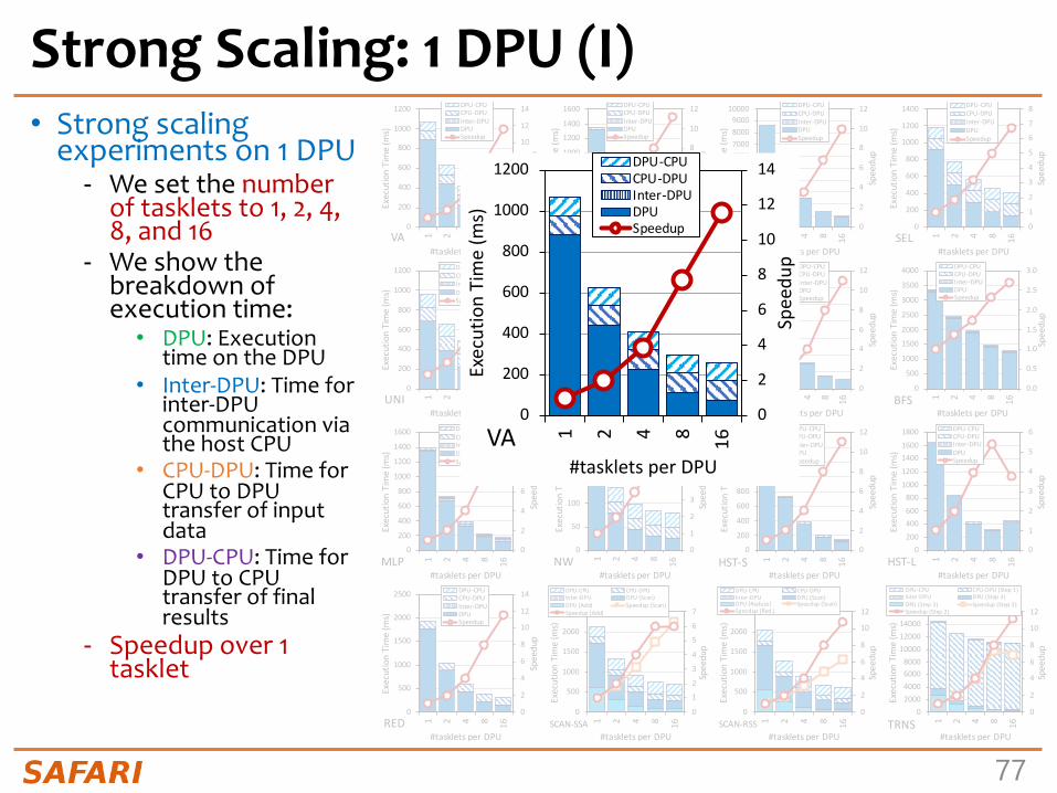
Strong Scaling: 1 DPU (I)• Strong scaling
experiments on 1 DPU- We set the number
of tasklets to 1, 2, 4, 8, and 16
- We show the breakdown of execution time:• DPU: Execution
time on the DPU• Inter-DPU: Time for
inter-DPU communication via the host CPU
• CPU-DPU: Time for CPU to DPU transfer of input data
• DPU-CPU: Time for DPU to CPU transfer of final results
- Speedup over 1 tasklet
0
2
4
6
8
10
12
14
0
200
400
600
800
1000
1200
1 2 4 8
16
Sp
ee
du
p
Exe
cu
tio
n T
ime
(m
s)
#tasklets per DPU
VA
DPU-CPU
CPU-DPU
Inter-DPU
DPU
Speedup
0
2
4
6
8
10
12
0
200
400
600
800
1000
1200
1400
1600
1 2 4 8
16
Sp
ee
du
p
Exe
cu
tio
n T
ime
(m
s)
#tasklets per DPU
GEMV
DPU-CPU
CPU-DPU
Inter-DPU
DPU
Speedup
0
2
4
6
8
10
12
0
1000
2000
3000
4000
5000
6000
7000
8000
9000
10000
1 2 4 8
16
Sp
ee
du
p
Exe
cu
tio
n T
ime
(m
s)
#tasklets per DPU
SpMV
DPU-CPU
CPU-DPU
Inter-DPU
DPU
Speedup
0
1
2
3
4
5
6
7
8
0
200
400
600
800
1000
1200
1400
1 2 4 8
16
Sp
ee
du
p
Exe
cu
tio
n T
ime
(m
s)
#tasklets per DPU
SEL
DPU-CPU
CPU-DPU
Inter-DPU
DPU
Speedup
0
1
2
3
4
5
6
7
8
0
200
400
600
800
1000
1200
1 2 4 8
16
Sp
ee
du
p
Exe
cu
tio
n T
ime
(m
s)
#tasklets per DPU
UNI
DPU-CPU
CPU-DPU
Inter-DPU
DPU
Speedup
0
1
2
3
4
5
6
0
2000
4000
6000
8000
10000
12000
14000
1 2 4 8
16
Sp
ee
du
p
Exe
cu
tio
n T
ime
(m
s)
#tasklets per DPU
BS
DPU-CPU
CPU-DPU
Inter-DPU
DPU
Speedup
0
2
4
6
8
10
12
0
20000
40000
60000
80000
100000
120000
140000
1 2 4 8
16
Sp
ee
du
p
Exe
cu
tio
n T
ime
(m
s)
#tasklets per DPU
TS
DPU-CPU
CPU-DPU
Inter-DPU
DPU
Speedup
0.0
0.5
1.0
1.5
2.0
2.5
3.0
0
500
1000
1500
2000
2500
3000
3500
4000
1 2 4 8
16
Sp
ee
du
p
Exe
cu
tio
n T
ime
(m
s)
#tasklets per DPU
BFS
DPU-CPU
CPU-DPU
Inter-DPU
DPU
Speedup
0
2
4
6
8
10
12
0
200
400
600
800
1000
1200
1400
16001 2 4 8
16
Sp
ee
du
p
Exe
cu
tio
n T
ime
(m
s)
#tasklets per DPU
MLP
DPU-CPU
CPU-DPU
Inter-DPU
DPU
Speedup
0
1
2
3
4
5
6
7
0
50
100
150
200
250
1 2 4 8
16
Sp
ee
du
p
Exe
cu
tio
n T
ime
(m
s)
#tasklets per DPU
NW
DPU-CPU
CPU-DPU
Inter-DPU
DPU
Speedup
0
2
4
6
8
10
12
14
0
500
1000
1500
2000
2500
1 2 4 8
16
Sp
ee
du
p
Exe
cu
tio
n T
ime
(m
s)
#tasklets per DPU
RED
DPU-CPU
CPU-DPU
Inter-DPU
DPU
Speedup
0
1
2
3
4
5
6
7
0
500
1000
1500
2000
2500
1 2 4 8
16
Sp
ee
du
p
Exe
cu
tio
n T
ime
(m
s)
#tasklets per DPU
SCAN-SSA
DPU-CPU CPU-DPU
Inter-DPU DPU (Scan)
DPU (Add) Speedup (Scan)
Speedup (Add)
0
2
4
6
8
10
12
0
500
1000
1500
2000
2500
1 2 4 8
16
Sp
ee
du
p
Exe
cu
tio
n T
ime
(m
s)
#tasklets per DPU
SCAN-RSS
DPU-CPU CPU-DPU
Inter-DPU DPU (Scan)
DPU (Reduce) Speedup (Scan)
Speedup (Red.)
0
2
4
6
8
10
12
0
2000
4000
6000
8000
10000
12000
14000
16000
1 2 4 8
16
Sp
ee
du
p
Exe
cu
tio
n T
ime
(m
s)
#tasklets per DPU
TRNS
DPU-CPU CPU-DPU (Step 1)
Inter-DPU DPU (Step 3)
DPU (Step 2) Speedup (Step 3)
Speedup (Step 2)
0
1
2
3
4
5
6
0
200
400
600
800
1000
1200
1400
1600
1800
1 2 4 8
16
Sp
ee
du
p
Exe
cu
tio
n T
ime
(m
s)
#tasklets per DPU
HST-L
DPU-CPU
CPU-DPU
Inter-DPU
DPU
Speedup
0
2
4
6
8
10
12
0
200
400
600
800
1000
1200
1400
1600
1 2 4 8
16
Sp
ee
du
p
Exe
cu
tio
n T
ime
(m
s)
#tasklets per DPU
HST-S
DPU-CPU
CPU-DPU
Inter-DPU
DPU
Speedup
0
2
4
6
8
10
12
14
0
200
400
600
800
1000
1200
1 2 4 8 16
Spee
dup
Exec
utio
n Ti
me
(ms)#tasklets per DPU
VA
DPU-CPUCPU-DPUInter-DPUDPUSpeedup

78
0
2
4
6
8
10
12
14
0
200
400
600
800
1000
1200
1 2 4 8
16
Sp
ee
du
p
Exe
cu
tio
n T
ime
(m
s)
#tasklets per DPU
VA
DPU-CPU
CPU-DPU
Inter-DPU
DPU
Speedup
0
2
4
6
8
10
12
0
200
400
600
800
1000
1200
1400
1600
1 2 4 8
16
Sp
ee
du
p
Exe
cu
tio
n T
ime
(m
s)
#tasklets per DPU
GEMV
DPU-CPU
CPU-DPU
Inter-DPU
DPU
Speedup
0
2
4
6
8
10
12
0
1000
2000
3000
4000
5000
6000
7000
8000
9000
10000
1 2 4 8
16
Sp
ee
du
p
Exe
cu
tio
n T
ime
(m
s)
#tasklets per DPU
SpMV
DPU-CPU
CPU-DPU
Inter-DPU
DPU
Speedup
0
1
2
3
4
5
6
7
8
0
200
400
600
800
1000
1200
1400
1 2 4 8
16
Sp
ee
du
p
Exe
cu
tio
n T
ime
(m
s)
#tasklets per DPU
SEL
DPU-CPU
CPU-DPU
Inter-DPU
DPU
Speedup
0
1
2
3
4
5
6
7
8
0
200
400
600
800
1000
1200
1 2 4 8
16
Sp
ee
du
p
Exe
cu
tio
n T
ime
(m
s)
#tasklets per DPU
UNI
DPU-CPU
CPU-DPU
Inter-DPU
DPU
Speedup
0
1
2
3
4
5
6
0
2000
4000
6000
8000
10000
12000
14000
1 2 4 8
16
Sp
ee
du
p
Exe
cu
tio
n T
ime
(m
s)
#tasklets per DPU
BS
DPU-CPU
CPU-DPU
Inter-DPU
DPU
Speedup
0
2
4
6
8
10
12
0
20000
40000
60000
80000
100000
120000
140000
1 2 4 8
16
Sp
ee
du
p
Exe
cu
tio
n T
ime
(m
s)
#tasklets per DPU
TS
DPU-CPU
CPU-DPU
Inter-DPU
DPU
Speedup
0.0
0.5
1.0
1.5
2.0
2.5
3.0
0
500
1000
1500
2000
2500
3000
3500
4000
1 2 4 8
16
Sp
ee
du
p
Exe
cu
tio
n T
ime
(m
s)
#tasklets per DPU
BFS
DPU-CPU
CPU-DPU
Inter-DPU
DPU
Speedup
0
2
4
6
8
10
12
0
200
400
600
800
1000
1200
1400
1600
1 2 4 8
16
Sp
ee
du
p
Exe
cu
tio
n T
ime
(m
s)
#tasklets per DPU
MLP
DPU-CPU
CPU-DPU
Inter-DPU
DPU
Speedup
0
1
2
3
4
5
6
7
0
50
100
150
200
250
1 2 4 8
16
Sp
ee
du
p
Exe
cu
tio
n T
ime
(m
s)
#tasklets per DPU
NW
DPU-CPU
CPU-DPU
Inter-DPU
DPU
Speedup
0
2
4
6
8
10
12
14
0
500
1000
1500
2000
2500
1 2 4 8
16
Sp
ee
du
p
Exe
cu
tio
n T
ime
(m
s)
#tasklets per DPU
RED
DPU-CPU
CPU-DPU
Inter-DPU
DPU
Speedup
0
1
2
3
4
5
6
7
0
500
1000
1500
2000
2500
1 2 4 8
16
Sp
ee
du
p
Exe
cu
tio
n T
ime
(m
s)
#tasklets per DPU
SCAN-SSA
DPU-CPU CPU-DPU
Inter-DPU DPU (Scan)
DPU (Add) Speedup (Scan)
Speedup (Add)
0
2
4
6
8
10
12
0
500
1000
1500
2000
2500
1 2 4 8
16
Sp
ee
du
p
Exe
cu
tio
n T
ime
(m
s)
#tasklets per DPU
SCAN-RSS
DPU-CPU CPU-DPU
Inter-DPU DPU (Scan)
DPU (Reduce) Speedup (Scan)
Speedup (Red.)
0
2
4
6
8
10
12
0
2000
4000
6000
8000
10000
12000
14000
16000
1 2 4 8
16
Sp
ee
du
p
Exe
cu
tio
n T
ime
(m
s)
#tasklets per DPU
TRNS
DPU-CPU CPU-DPU (Step 1)
Inter-DPU DPU (Step 3)
DPU (Step 2) Speedup (Step 3)
Speedup (Step 2)
0
1
2
3
4
5
6
0
200
400
600
800
1000
1200
1400
1600
1800
1 2 4 8
16
Sp
ee
du
p
Exe
cu
tio
n T
ime
(m
s)
#tasklets per DPU
HST-L
DPU-CPU
CPU-DPU
Inter-DPU
DPU
Speedup
0
2
4
6
8
10
12
0
200
400
600
800
1000
1200
1400
1600
1 2 4 8
16
Sp
ee
du
p
Exe
cu
tio
n T
ime
(m
s)
#tasklets per DPU
HST-S
DPU-CPU
CPU-DPU
Inter-DPU
DPU
Speedup
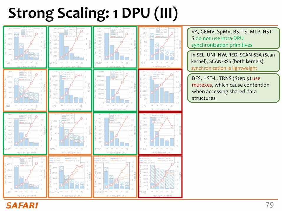
Strong Scaling: 1 DPU (II)VA, GEMV, SpMV, SEL, UNI, TS, MLP, NW, HST-S, RED, SCAN-SSA (Scan kernel), SCAN-RSS (both kernels), and TRNS (Step 2 kernel), the best performing number of tasklets is 16
Speedups 1.5-2.0x as we double the number of tasklets from 1 to 8.Speedups 1.2-1.5x from 8 to 16, since the pipeline throughput saturates at 11 tasklets
KEYOBSERVATION10Anumberoftaskletsgreaterthan11isagoodchoiceformostreal-worldworkloadswetested(16kernelsoutof19kernelsfrom16benchmarks),asitfullyutilizestheDPU’spipeline.
79
0
2
4
6
8
10
12
14
0
200
400
600
800
1000
1200
1 2 4 8
16
Sp
ee
du
p
Exe
cu
tio
n T
ime
(m
s)
#tasklets per DPU
VA
DPU-CPU
CPU-DPU
Inter-DPU
DPU
Speedup
0
2
4
6
8
10
12
0
200
400
600
800
1000
1200
1400
1600
1 2 4 8
16
Sp
ee
du
p
Exe
cu
tio
n T
ime
(m
s)
#tasklets per DPU
GEMV
DPU-CPU
CPU-DPU
Inter-DPU
DPU
Speedup
0
2
4
6
8
10
12
0
1000
2000
3000
4000
5000
6000
7000
8000
9000
10000
1 2 4 8
16
Sp
ee
du
p
Exe
cu
tio
n T
ime
(m
s)
#tasklets per DPU
SpMV
DPU-CPU
CPU-DPU
Inter-DPU
DPU
Speedup
0
1
2
3
4
5
6
7
8
0
200
400
600
800
1000
1200
1400
1 2 4 8
16
Sp
ee
du
p
Exe
cu
tio
n T
ime
(m
s)
#tasklets per DPU
SEL
DPU-CPU
CPU-DPU
Inter-DPU
DPU
Speedup
0
1
2
3
4
5
6
7
8
0
200
400
600
800
1000
1200
1 2 4 8
16
Sp
ee
du
p
Exe
cu
tio
n T
ime
(m
s)
#tasklets per DPU
UNI
DPU-CPU
CPU-DPU
Inter-DPU
DPU
Speedup
0
1
2
3
4
5
6
0
2000
4000
6000
8000
10000
12000
14000
1 2 4 8
16
Sp
ee
du
p
Exe
cu
tio
n T
ime
(m
s)
#tasklets per DPU
BS
DPU-CPU
CPU-DPU
Inter-DPU
DPU
Speedup
0
2
4
6
8
10
12
0
20000
40000
60000
80000
100000
120000
140000
1 2 4 8
16
Sp
ee
du
p
Exe
cu
tio
n T
ime
(m
s)
#tasklets per DPU
TS
DPU-CPU
CPU-DPU
Inter-DPU
DPU
Speedup
0.0
0.5
1.0
1.5
2.0
2.5
3.0
0
500
1000
1500
2000
2500
3000
3500
4000
1 2 4 8
16
Sp
ee
du
p
Exe
cu
tio
n T
ime
(m
s)
#tasklets per DPU
BFS
DPU-CPU
CPU-DPU
Inter-DPU
DPU
Speedup
0
2
4
6
8
10
12
0
200
400
600
800
1000
1200
1400
1600
1 2 4 8
16
Sp
ee
du
p
Exe
cu
tio
n T
ime
(m
s)
#tasklets per DPU
MLP
DPU-CPU
CPU-DPU
Inter-DPU
DPU
Speedup
0
1
2
3
4
5
6
7
0
50
100
150
200
250
1 2 4 8
16
Sp
ee
du
p
Exe
cu
tio
n T
ime
(m
s)
#tasklets per DPU
NW
DPU-CPU
CPU-DPU
Inter-DPU
DPU
Speedup
0
2
4
6
8
10
12
14
0
500
1000
1500
2000
2500
1 2 4 8
16
Sp
ee
du
p
Exe
cu
tio
n T
ime
(m
s)
#tasklets per DPU
RED
DPU-CPU
CPU-DPU
Inter-DPU
DPU
Speedup
0
1
2
3
4
5
6
7
0
500
1000
1500
2000
2500
1 2 4 8
16
Sp
ee
du
p
Exe
cu
tio
n T
ime
(m
s)
#tasklets per DPU
SCAN-SSA
DPU-CPU CPU-DPU
Inter-DPU DPU (Scan)
DPU (Add) Speedup (Scan)
Speedup (Add)
0
2
4
6
8
10
12
0
500
1000
1500
2000
2500
1 2 4 8
16
Sp
ee
du
p
Exe
cu
tio
n T
ime
(m
s)
#tasklets per DPU
SCAN-RSS
DPU-CPU CPU-DPU
Inter-DPU DPU (Scan)
DPU (Reduce) Speedup (Scan)
Speedup (Red.)
0
2
4
6
8
10
12
0
2000
4000
6000
8000
10000
12000
14000
16000
1 2 4 8
16
Sp
ee
du
p
Exe
cu
tio
n T
ime
(m
s)
#tasklets per DPU
TRNS
DPU-CPU CPU-DPU (Step 1)
Inter-DPU DPU (Step 3)
DPU (Step 2) Speedup (Step 3)
Speedup (Step 2)
0
1
2
3
4
5
6
0
200
400
600
800
1000
1200
1400
1600
1800
1 2 4 8
16
Sp
ee
du
p
Exe
cu
tio
n T
ime
(m
s)
#tasklets per DPU
HST-L
DPU-CPU
CPU-DPU
Inter-DPU
DPU
Speedup
0
2
4
6
8
10
12
0
200
400
600
800
1000
1200
1400
1600
1 2 4 8
16
Sp
ee
du
p
Exe
cu
tio
n T
ime
(m
s)
#tasklets per DPU
HST-S
DPU-CPU
CPU-DPU
Inter-DPU
DPU
Speedup
Strong Scaling: 1 DPU (III)VA, GEMV, SpMV, BS, TS, MLP, HST-S do not use intra-DPU synchronization primitives
BFS, HST-L, TRNS (Step 3) use mutexes, which cause contention when accessing shared data structures
In SEL, UNI, NW, RED, SCAN-SSA (Scan kernel), SCAN-RSS (both kernels), synchronization is lightweight

80
0
2
4
6
8
10
12
14
0
200
400
600
800
1000
1200
1 2 4 8
16
Sp
ee
du
p
Exe
cu
tio
n T
ime
(m
s)
#tasklets per DPU
VA
DPU-CPU
CPU-DPU
Inter-DPU
DPU
Speedup
0
2
4
6
8
10
12
0
200
400
600
800
1000
1200
1400
1600
1 2 4 8
16
Sp
ee
du
p
Exe
cu
tio
n T
ime
(m
s)
#tasklets per DPU
GEMV
DPU-CPU
CPU-DPU
Inter-DPU
DPU
Speedup
0
2
4
6
8
10
12
0
1000
2000
3000
4000
5000
6000
7000
8000
9000
10000
1 2 4 8
16
Sp
ee
du
p
Exe
cu
tio
n T
ime
(m
s)
#tasklets per DPU
SpMV
DPU-CPU
CPU-DPU
Inter-DPU
DPU
Speedup
0
1
2
3
4
5
6
7
8
0
200
400
600
800
1000
1200
1400
1 2 4 8
16
Sp
ee
du
p
Exe
cu
tio
n T
ime
(m
s)
#tasklets per DPU
SEL
DPU-CPU
CPU-DPU
Inter-DPU
DPU
Speedup
0
1
2
3
4
5
6
7
8
0
200
400
600
800
1000
1200
1 2 4 8
16
Sp
ee
du
p
Exe
cu
tio
n T
ime
(m
s)
#tasklets per DPU
UNI
DPU-CPU
CPU-DPU
Inter-DPU
DPU
Speedup
0
1
2
3
4
5
6
0
2000
4000
6000
8000
10000
12000
14000
1 2 4 8
16
Sp
ee
du
p
Exe
cu
tio
n T
ime
(m
s)
#tasklets per DPU
BS
DPU-CPU
CPU-DPU
Inter-DPU
DPU
Speedup
0
2
4
6
8
10
12
0
20000
40000
60000
80000
100000
120000
140000
1 2 4 8
16
Sp
ee
du
p
Exe
cu
tio
n T
ime
(m
s)
#tasklets per DPU
TS
DPU-CPU
CPU-DPU
Inter-DPU
DPU
Speedup
0.0
0.5
1.0
1.5
2.0
2.5
3.0
0
500
1000
1500
2000
2500
3000
3500
4000
1 2 4 8
16
Sp
ee
du
p
Exe
cu
tio
n T
ime
(m
s)
#tasklets per DPU
BFS
DPU-CPU
CPU-DPU
Inter-DPU
DPU
Speedup
0
2
4
6
8
10
12
0
200
400
600
800
1000
1200
1400
1600
1 2 4 8
16
Sp
ee
du
p
Exe
cu
tio
n T
ime
(m
s)
#tasklets per DPU
MLP
DPU-CPU
CPU-DPU
Inter-DPU
DPU
Speedup
0
1
2
3
4
5
6
7
0
50
100
150
200
250
1 2 4 8
16
Sp
ee
du
p
Exe
cu
tio
n T
ime
(m
s)
#tasklets per DPU
NW
DPU-CPU
CPU-DPU
Inter-DPU
DPU
Speedup
0
2
4
6
8
10
12
14
0
500
1000
1500
2000
2500
1 2 4 8
16
Sp
ee
du
p
Exe
cu
tio
n T
ime
(m
s)
#tasklets per DPU
RED
DPU-CPU
CPU-DPU
Inter-DPU
DPU
Speedup
0
1
2
3
4
5
6
7
0
500
1000
1500
2000
2500
1 2 4 8
16
Sp
ee
du
p
Exe
cu
tio
n T
ime
(m
s)
#tasklets per DPU
SCAN-SSA
DPU-CPU CPU-DPU
Inter-DPU DPU (Scan)
DPU (Add) Speedup (Scan)
Speedup (Add)
0
2
4
6
8
10
12
0
500
1000
1500
2000
2500
1 2 4 8
16
Sp
ee
du
p
Exe
cu
tio
n T
ime
(m
s)
#tasklets per DPU
SCAN-RSS
DPU-CPU CPU-DPU
Inter-DPU DPU (Scan)
DPU (Reduce) Speedup (Scan)
Speedup (Red.)
0
2
4
6
8
10
12
0
2000
4000
6000
8000
10000
12000
14000
16000
1 2 4 8
16
Sp
ee
du
p
Exe
cu
tio
n T
ime
(m
s)
#tasklets per DPU
TRNS
DPU-CPU CPU-DPU (Step 1)
Inter-DPU DPU (Step 3)
DPU (Step 2) Speedup (Step 3)
Speedup (Step 2)
0
1
2
3
4
5
6
0
200
400
600
800
1000
1200
1400
1600
1800
1 2 4 8
16
Sp
ee
du
p
Exe
cu
tio
n T
ime
(m
s)
#tasklets per DPU
HST-L
DPU-CPU
CPU-DPU
Inter-DPU
DPU
Speedup
0
2
4
6
8
10
12
0
200
400
600
800
1000
1200
1400
1600
1 2 4 8
16
Sp
ee
du
p
Exe
cu
tio
n T
ime
(m
s)
#tasklets per DPU
HST-S
DPU-CPU
CPU-DPU
Inter-DPU
DPU
Speedup
Strong Scaling: 1 DPU (IV)
0
1
2
3
4
5
6
0200400600800
10001200140016001800
1 2 4 8 16
Spee
dup
Exec
utio
n Ti
me
(ms)
#tasklets per DPUHST-L
DPU-CPUCPU-DPUInter-DPUDPUSpeedup
VA, GEMV, SpMV, BS, TS, MLP, HST-S do not use synchronization primitives
BFS, HST-L, TRNS (Step 3) use mutexes, which cause contention when accessing shared data structures
KEYOBSERVATION11Intensiveuseofintra-DPUsynchronizationacrosstasklets (e.g.,mutexes,barriers,handshakes)maylimitscalability,sometimescausingthebestperformingnumberoftasklets tobelowerthan11.
In SEL, UNI, NW, RED, SCAN-SSA (Scan kernel), SCAN-RSS (both kernels), synchronization is lightweight
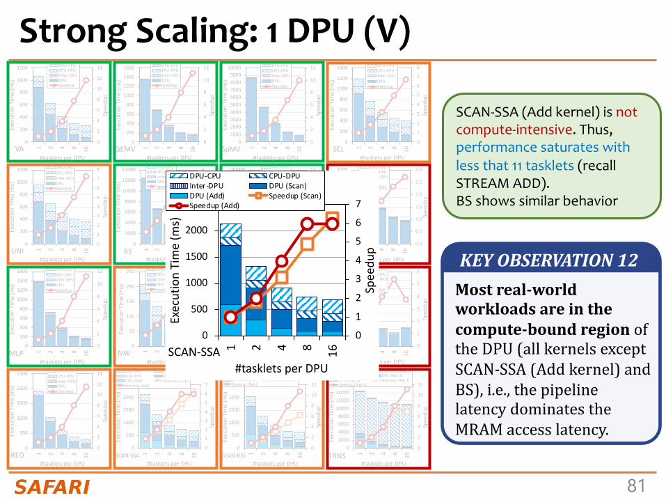
81
0
2
4
6
8
10
12
14
0
200
400
600
800
1000
1200
1 2 4 8
16
Sp
ee
du
p
Exe
cu
tio
n T
ime
(m
s)
#tasklets per DPU
VA
DPU-CPU
CPU-DPU
Inter-DPU
DPU
Speedup
0
2
4
6
8
10
12
0
200
400
600
800
1000
1200
1400
1600
1 2 4 8
16
Sp
ee
du
p
Exe
cu
tio
n T
ime
(m
s)
#tasklets per DPU
GEMV
DPU-CPU
CPU-DPU
Inter-DPU
DPU
Speedup
0
2
4
6
8
10
12
0
1000
2000
3000
4000
5000
6000
7000
8000
9000
10000
1 2 4 8
16
Sp
ee
du
p
Exe
cu
tio
n T
ime
(m
s)
#tasklets per DPU
SpMV
DPU-CPU
CPU-DPU
Inter-DPU
DPU
Speedup
0
1
2
3
4
5
6
7
8
0
200
400
600
800
1000
1200
1400
1 2 4 8
16
Sp
ee
du
p
Exe
cu
tio
n T
ime
(m
s)
#tasklets per DPU
SEL
DPU-CPU
CPU-DPU
Inter-DPU
DPU
Speedup
0
1
2
3
4
5
6
7
8
0
200
400
600
800
1000
1200
1 2 4 8
16
Sp
ee
du
p
Exe
cu
tio
n T
ime
(m
s)
#tasklets per DPU
UNI
DPU-CPU
CPU-DPU
Inter-DPU
DPU
Speedup
0
1
2
3
4
5
6
0
2000
4000
6000
8000
10000
12000
14000
1 2 4 8
16
Sp
ee
du
p
Exe
cu
tio
n T
ime
(m
s)
#tasklets per DPU
BS
DPU-CPU
CPU-DPU
Inter-DPU
DPU
Speedup
0
2
4
6
8
10
12
0
20000
40000
60000
80000
100000
120000
140000
1 2 4 8
16
Sp
ee
du
p
Exe
cu
tio
n T
ime
(m
s)
#tasklets per DPU
TS
DPU-CPU
CPU-DPU
Inter-DPU
DPU
Speedup
0.0
0.5
1.0
1.5
2.0
2.5
3.0
0
500
1000
1500
2000
2500
3000
3500
4000
1 2 4 8
16
Sp
ee
du
p
Exe
cu
tio
n T
ime
(m
s)
#tasklets per DPU
BFS
DPU-CPU
CPU-DPU
Inter-DPU
DPU
Speedup
0
2
4
6
8
10
12
0
200
400
600
800
1000
1200
1400
1600
1 2 4 8
16
Sp
ee
du
p
Exe
cu
tio
n T
ime
(m
s)
#tasklets per DPU
MLP
DPU-CPU
CPU-DPU
Inter-DPU
DPU
Speedup
0
1
2
3
4
5
6
7
0
50
100
150
200
250
1 2 4 8
16
Sp
ee
du
p
Exe
cu
tio
n T
ime
(m
s)
#tasklets per DPU
NW
DPU-CPU
CPU-DPU
Inter-DPU
DPU
Speedup
0
2
4
6
8
10
12
14
0
500
1000
1500
2000
2500
1 2 4 8
16
Sp
ee
du
p
Exe
cu
tio
n T
ime
(m
s)
#tasklets per DPU
RED
DPU-CPU
CPU-DPU
Inter-DPU
DPU
Speedup
0
1
2
3
4
5
6
7
0
500
1000
1500
2000
2500
1 2 4 8
16
Sp
ee
du
p
Exe
cu
tio
n T
ime
(m
s)
#tasklets per DPU
SCAN-SSA
DPU-CPU CPU-DPU
Inter-DPU DPU (Scan)
DPU (Add) Speedup (Scan)
Speedup (Add)
0
2
4
6
8
10
12
0
500
1000
1500
2000
2500
1 2 4 8
16
Sp
ee
du
p
Exe
cu
tio
n T
ime
(m
s)
#tasklets per DPU
SCAN-RSS
DPU-CPU CPU-DPU
Inter-DPU DPU (Scan)
DPU (Reduce) Speedup (Scan)
Speedup (Red.)
0
2
4
6
8
10
12
0
2000
4000
6000
8000
10000
12000
14000
16000
1 2 4 8
16
Sp
ee
du
p
Exe
cu
tio
n T
ime
(m
s)
#tasklets per DPU
TRNS
DPU-CPU CPU-DPU (Step 1)
Inter-DPU DPU (Step 3)
DPU (Step 2) Speedup (Step 3)
Speedup (Step 2)
0
1
2
3
4
5
6
0
200
400
600
800
1000
1200
1400
1600
1800
1 2 4 8
16
Sp
ee
du
p
Exe
cu
tio
n T
ime
(m
s)
#tasklets per DPU
HST-L
DPU-CPU
CPU-DPU
Inter-DPU
DPU
Speedup
0
2
4
6
8
10
12
0
200
400
600
800
1000
1200
1400
1600
1 2 4 8
16
Sp
ee
du
p
Exe
cu
tio
n T
ime
(m
s)
#tasklets per DPU
HST-S
DPU-CPU
CPU-DPU
Inter-DPU
DPU
Speedup
Strong Scaling: 1 DPU (V)
0
1
2
3
4
5
6
7
0
500
1000
1500
2000
2500
1 2 4 8 16
Spee
dup
Exec
utio
n Ti
me
(ms)
#tasklets per DPUSCAN-SSA
DPU-CPU CPU-DPUInter-DPU DPU (Scan)DPU (Add) Speedup (Scan)Speedup (Add)
SCAN-SSA (Add kernel) is not compute-intensive. Thus, performance saturates with less that 11 tasklets (recall STREAM ADD).BS shows similar behavior
KEYOBSERVATION12Mostreal-worldworkloadsareinthecompute-boundregionoftheDPU(allkernelsexceptSCAN-SSA(Addkernel)andBS),i.e.,thepipelinelatencydominatestheMRAMaccesslatency.

82
0
2
4
6
8
10
12
14
0
200
400
600
800
1000
1200
1 2 4 8
16
Sp
ee
du
p
Exe
cu
tio
n T
ime
(m
s)
#tasklets per DPU
VA
DPU-CPU
CPU-DPU
Inter-DPU
DPU
Speedup
0
2
4
6
8
10
12
0
200
400
600
800
1000
1200
1400
1600
1 2 4 8
16
Sp
ee
du
p
Exe
cu
tio
n T
ime
(m
s)
#tasklets per DPU
GEMV
DPU-CPU
CPU-DPU
Inter-DPU
DPU
Speedup
0
2
4
6
8
10
12
0
1000
2000
3000
4000
5000
6000
7000
8000
9000
10000
1 2 4 8
16
Sp
ee
du
p
Exe
cu
tio
n T
ime
(m
s)
#tasklets per DPU
SpMV
DPU-CPU
CPU-DPU
Inter-DPU
DPU
Speedup
0
1
2
3
4
5
6
7
8
0
200
400
600
800
1000
1200
1400
1 2 4 8
16
Sp
ee
du
p
Exe
cu
tio
n T
ime
(m
s)
#tasklets per DPU
SEL
DPU-CPU
CPU-DPU
Inter-DPU
DPU
Speedup
0
1
2
3
4
5
6
7
8
0
200
400
600
800
1000
1200
1 2 4 8
16
Sp
ee
du
p
Exe
cu
tio
n T
ime
(m
s)
#tasklets per DPU
UNI
DPU-CPU
CPU-DPU
Inter-DPU
DPU
Speedup
0
1
2
3
4
5
6
0
2000
4000
6000
8000
10000
12000
14000
1 2 4 8
16
Sp
ee
du
p
Exe
cu
tio
n T
ime
(m
s)
#tasklets per DPU
BS
DPU-CPU
CPU-DPU
Inter-DPU
DPU
Speedup
0
2
4
6
8
10
12
0
20000
40000
60000
80000
100000
120000
140000
1 2 4 8
16
Sp
ee
du
p
Exe
cu
tio
n T
ime
(m
s)
#tasklets per DPU
TS
DPU-CPU
CPU-DPU
Inter-DPU
DPU
Speedup
0.0
0.5
1.0
1.5
2.0
2.5
3.0
0
500
1000
1500
2000
2500
3000
3500
4000
1 2 4 8
16
Sp
ee
du
p
Exe
cu
tio
n T
ime
(m
s)
#tasklets per DPU
BFS
DPU-CPU
CPU-DPU
Inter-DPU
DPU
Speedup
0
2
4
6
8
10
12
0
200
400
600
800
1000
1200
1400
1600
1 2 4 8
16
Sp
ee
du
p
Exe
cu
tio
n T
ime
(m
s)
#tasklets per DPU
MLP
DPU-CPU
CPU-DPU
Inter-DPU
DPU
Speedup
0
1
2
3
4
5
6
7
0
50
100
150
200
250
1 2 4 8
16
Sp
ee
du
p
Exe
cu
tio
n T
ime
(m
s)
#tasklets per DPU
NW
DPU-CPU
CPU-DPU
Inter-DPU
DPU
Speedup
0
2
4
6
8
10
12
14
0
500
1000
1500
2000
2500
1 2 4 8
16
Sp
ee
du
p
Exe
cu
tio
n T
ime
(m
s)
#tasklets per DPU
RED
DPU-CPU
CPU-DPU
Inter-DPU
DPU
Speedup
0
1
2
3
4
5
6
7
0
500
1000
1500
2000
2500
1 2 4 8
16
Sp
ee
du
p
Exe
cu
tio
n T
ime
(m
s)
#tasklets per DPU
SCAN-SSA
DPU-CPU CPU-DPU
Inter-DPU DPU (Scan)
DPU (Add) Speedup (Scan)
Speedup (Add)
0
2
4
6
8
10
12
0
500
1000
1500
2000
2500
1 2 4 8
16
Sp
ee
du
p
Exe
cu
tio
n T
ime
(m
s)
#tasklets per DPU
SCAN-RSS
DPU-CPU CPU-DPU
Inter-DPU DPU (Scan)
DPU (Reduce) Speedup (Scan)
Speedup (Red.)
0
2
4
6
8
10
12
0
2000
4000
6000
8000
10000
12000
14000
16000
1 2 4 8
16
Sp
ee
du
p
Exe
cu
tio
n T
ime
(m
s)
#tasklets per DPU
TRNS
DPU-CPU CPU-DPU (Step 1)
Inter-DPU DPU (Step 3)
DPU (Step 2) Speedup (Step 3)
Speedup (Step 2)
0
1
2
3
4
5
6
0
200
400
600
800
1000
1200
1400
1600
1800
1 2 4 8
16
Sp
ee
du
p
Exe
cu
tio
n T
ime
(m
s)
#tasklets per DPU
HST-L
DPU-CPU
CPU-DPU
Inter-DPU
DPU
Speedup
0
2
4
6
8
10
12
0
200
400
600
800
1000
1200
1400
1600
1 2 4 8
16
Sp
ee
du
p
Exe
cu
tio
n T
ime
(m
s)
#tasklets per DPU
HST-S
DPU-CPU
CPU-DPU
Inter-DPU
DPU
Speedup
Strong Scaling: 1 DPU (VI)
TRNS performs step 1 of the matrix transposition via the CPU-DPU transfer.Using small transfers (8 elements) does not exploit full CPU-DPU bandwidth
KEYOBSERVATION13Transferringlargedatachunksfrom/tothehostCPUispreferredforinputdataandoutputresultsduetohighersustainedCPU-DPU/DPU-CPUbandwidths.
The amount of time spent on CPU-DPU and DPU-CPU transfers is lowcompared to the time spent on DPU execution
0
2
4
6
8
10
12
02000400060008000
10000120001400016000
1 2 4 8 16
Spee
dup
Exec
utio
n Ti
me
(ms)
#tasklets per DPUTRNS
DPU-CPU CPU-DPU (Step 1)Inter-DPU DPU (Step 3)DPU (Step 2) Speedup (Step 3)Speedup (Step 2)
https://arxiv.org/pdf/2105.03814.pdfhttps://github.com/CMU-SAFARI/prim-benchmarks

83
• Strong scaling experiments on 1 rank- We set the number of
tasklets to the best performing one
- The number of DPUs is 1, 4, 16, 64
- We show the breakdown of execution time:• DPU: Execution time
on the DPU• Inter-DPU: Time for
inter-DPU communication via the host CPU
• CPU-DPU: Time for CPU to DPU transfer of input data
• DPU-CPU: Time for DPU to CPU transfer of final results
- Speedup over 1 DPU
0
10
20
30
40
50
60
0
50
100
150
200
250
300
1 4 16 64
Spee
dup
Exec
utio
n Ti
me
(ms)
#DPUsVA
DPU-CPUCPU-DPUInter-DPUDPUSpeedup
0
10
20
30
40
50
60
70
0
100
200
300
400
500
600
700
1 4 16 64
Spee
dup
Exec
utio
n Ti
me
(ms)
#DPUsGEMV
DPU-CPUCPU-DPUInter-DPUDPUSpeedup
0
5
10
15
20
25
30
35
40
0
100
200300
400
500
600700
800
9001000
1 4 16 64
Spee
dup
Exec
utio
n Ti
me
(ms)
#DPUsSpMV
DPU-CPUCPU-DPUInter-DPUDPUSpeedup
0
10
20
30
40
50
60
70
0
50
100
150
200
250
300
350
400
450
1 4 16 64
Spee
dup
Exec
utio
n Ti
me
(ms)
#DPUsSEL
DPU-CPUCPU-DPUInter-DPUDPUSpeedup
0
10
20
30
40
50
60
70
0
50
100
150
200
250
300
350
400
1 4 16 64
Spee
dup
Exec
utio
n Ti
me
(ms)
#DPUsUNI
DPU-CPUCPU-DPUInter-DPUDPUSpeedup
0
10
20
30
40
50
60
70
0
500
1000
1500
2000
2500
1 4 16 64
Spee
dup
Exec
utio
n Ti
me
(ms)
#DPUsBS
DPU-CPUCPU-DPUInter-DPUDPUSpeedup
0
10
20
30
40
50
60
70
0
2000
4000
6000
8000
10000
12000
1 4 16 64
Spee
dup
Exec
utio
n Ti
me
(ms)
#DPUsTS
DPU-CPUCPU-DPUInter-DPUDPUSpeedup
0
1
2
3
4
5
6
7
8
9
0
200
400
600
800
1000
1200
1400
1 4 16 64
Spee
dup
Exec
utio
n Ti
me
(ms)
#DPUsBFS
DPU-CPUCPU-DPUInter-DPUDPUSpeedup
0
10
20
30
40
50
60
70
0
200
400
600
800
1000
1200
14001 4 16 64
Spee
dup
Exec
utio
n Ti
me
(ms)
#DPUsMLP
DPU-CPUCPU-DPUInter-DPUDPUSpeedup
02
4
68
10
12
1416
18
20
0
500
1000
1500
2000
2500
1 4 16 64
Spee
dup
Exec
utio
n Ti
me
(ms)
#DPUsNW
DPU-CPUCPU-DPUInter-DPUDPUSpeedup
0
10
20
30
40
50
60
70
0
50
100
150
200
250
300
350
1 4 16 64
Spee
dup
Exec
utio
n Ti
me
(ms)
#DPUsRED
DPU-CPUCPU-DPUInter-DPUDPUSpeedup
0
10
20
30
40
50
60
70
0
100
200
300
400
500
600
700
800
1 4 16 64
Spee
dup
Exec
utio
n Ti
me
(ms)
#DPUsSCAN-SSA
DPU-CPU CPU-DPUInter-DPU DPU (Scan)DPU (Add) Speedup (Scan)Speedup (Add)
0
10
20
30
40
50
60
70
0.E+00
1.E+02
2.E+02
3.E+02
4.E+02
5.E+02
6.E+02
7.E+02
1 4 16 64
Spee
dup
Exec
utio
n Ti
me
(ms)
#DPUsSCAN-RSS
DPU-CPU CPU-DPUInter-DPU DPU (Scan)DPU (Reduce) Speedup (Scan)Speedup (Red.)
0
10
20
30
40
50
60
70
0.E+00
1.E+05
2.E+05
3.E+05
4.E+05
5.E+05
6.E+05
7.E+05
8.E+05
1 4 16 64
Spee
dup
Exec
utio
n Ti
me
(ms)
#DPUsTRNS
DPU-CPU CPU-DPU (Step 1)Inter-DPU DPU (Step 3)DPU (Step 2) Speedup (Step 3)Speedup (Step 2)
0
10
20
30
40
50
60
0
20
40
60
80
100
120
140
160
1 4
16 64
Spee
dup
Exec
utio
n Ti
me
(ms)
#DPUsHST-S
DPU-CPUCPU-DPUInter-DPUDPUSpeedup
0
10
20
30
40
50
60
70
050
100
150200
250
300
350400
450
500
1 4 16 64
Spee
dup
Exec
utio
n Ti
me
(ms)
#DPUsHST-L
DPU-CPUCPU-DPUInter-DPUDPUSpeedup
Strong Scaling: 1 Rank (I)
02468101214161820
0
500
1000
1500
2000
2500
1 4 16 64
Spee
dup
Exec
utio
n Ti
me
(ms)
#DPUsNW
DPU-CPUCPU-DPUInter-DPUDPUSpeedup

84
0
10
20
30
40
50
60
0
50
100
150
200
250
300
1 4 16 64
Spee
dup
Exec
utio
n Ti
me
(ms)
#DPUsVA
DPU-CPUCPU-DPUInter-DPUDPUSpeedup
0
10
20
30
40
50
60
70
0
100
200
300
400
500
600
700
1 4 16 64
Spee
dup
Exec
utio
n Ti
me
(ms)
#DPUsGEMV
DPU-CPUCPU-DPUInter-DPUDPUSpeedup
0
5
10
15
20
25
30
35
40
0
100
200300
400
500
600700
800
9001000
1 4 16 64
Spee
dup
Exec
utio
n Ti
me
(ms)
#DPUsSpMV
DPU-CPUCPU-DPUInter-DPUDPUSpeedup
0
10
20
30
40
50
60
70
0
50
100
150
200
250
300
350
400
450
1 4 16 64
Spee
dup
Exec
utio
n Ti
me
(ms)
#DPUsSEL
DPU-CPUCPU-DPUInter-DPUDPUSpeedup
0
10
20
30
40
50
60
70
0
50
100
150
200
250
300
350
400
1 4 16 64
Spee
dup
Exec
utio
n Ti
me
(ms)
#DPUsUNI
DPU-CPUCPU-DPUInter-DPUDPUSpeedup
0
10
20
30
40
50
60
70
0
500
1000
1500
2000
2500
1 4 16 64
Spee
dup
Exec
utio
n Ti
me
(ms)
#DPUsBS
DPU-CPUCPU-DPUInter-DPUDPUSpeedup
0
10
20
30
40
50
60
70
0
2000
4000
6000
8000
10000
12000
1 4 16 64
Spee
dup
Exec
utio
n Ti
me
(ms)
#DPUsTS
DPU-CPUCPU-DPUInter-DPUDPUSpeedup
0
1
2
3
4
5
6
7
8
9
0
200
400
600
800
1000
1200
1400
1 4 16 64
Spee
dup
Exec
utio
n Ti
me
(ms)
#DPUsBFS
DPU-CPUCPU-DPUInter-DPUDPUSpeedup
0
10
20
30
40
50
60
70
0
200
400
600
800
1000
1200
1400
1 4 16 64
Spee
dup
Exec
utio
n Ti
me
(ms)
#DPUsMLP
DPU-CPUCPU-DPUInter-DPUDPUSpeedup
02
4
68
10
12
1416
18
20
0
500
1000
1500
2000
2500
1 4 16 64
Spee
dup
Exec
utio
n Ti
me
(ms)
#DPUsNW
DPU-CPUCPU-DPUInter-DPUDPUSpeedup
0
10
20
30
40
50
60
70
0
50
100
150
200
250
300
350
1 4 16 64
Spee
dup
Exec
utio
n Ti
me
(ms)
#DPUsRED
DPU-CPUCPU-DPUInter-DPUDPUSpeedup
0
10
20
30
40
50
60
70
0
100
200
300
400
500
600
700
800
1 4 16 64
Spee
dup
Exec
utio
n Ti
me
(ms)
#DPUsSCAN-SSA
DPU-CPU CPU-DPUInter-DPU DPU (Scan)DPU (Add) Speedup (Scan)Speedup (Add)
0
10
20
30
40
50
60
70
0.E+00
1.E+02
2.E+02
3.E+02
4.E+02
5.E+02
6.E+02
7.E+02
1 4 16 64
Spee
dup
Exec
utio
n Ti
me
(ms)
#DPUsSCAN-RSS
DPU-CPU CPU-DPUInter-DPU DPU (Scan)DPU (Reduce) Speedup (Scan)Speedup (Red.)
0
10
20
30
40
50
60
70
0.E+00
1.E+05
2.E+05
3.E+05
4.E+05
5.E+05
6.E+05
7.E+05
8.E+05
1 4 16 64
Spee
dup
Exec
utio
n Ti
me
(ms)
#DPUsTRNS
DPU-CPU CPU-DPU (Step 1)Inter-DPU DPU (Step 3)DPU (Step 2) Speedup (Step 3)Speedup (Step 2)
0
10
20
30
40
50
60
0
20
40
60
80
100
120
140
160
1 4
16 64
Spee
dup
Exec
utio
n Ti
me
(ms)
#DPUsHST-S
DPU-CPUCPU-DPUInter-DPUDPUSpeedup
0
10
20
30
40
50
60
70
050
100
150200
250
300
350400
450
500
1 4 16 64
Spee
dup
Exec
utio
n Ti
me
(ms)
#DPUsHST-L
DPU-CPUCPU-DPUInter-DPUDPUSpeedup
Strong Scaling: 1 Rank (II)
VA, GEMV, SpMV, SEL, UNI, BS, TS, MLP, HST-S, HSTS-L, RED, SCAN-SSA (both kernel), SCAN-RSS (both kernels), and TRNS (both kernels) scale linearly with the number of DPUs
Scaling is sublinear for BFS and NW
BFS suffers load imbalance due to irregular graph topology
NW computes a diagonal of a 2D matrix in each iteration.More DPUs does not mean more parallelization in shorter diagonals.

85
0
10
20
30
40
50
60
0
50
100
150
200
250
300
1 4 16 64
Spee
dup
Exec
utio
n Ti
me
(ms)
#DPUsVA
DPU-CPUCPU-DPUInter-DPUDPUSpeedup
0
10
20
30
40
50
60
70
0
100
200
300
400
500
600
700
1 4 16 64
Spee
dup
Exec
utio
n Ti
me
(ms)
#DPUsGEMV
DPU-CPUCPU-DPUInter-DPUDPUSpeedup
0
5
10
15
20
25
30
35
40
0
100
200300
400
500
600700
800
9001000
1 4 16 64
Spee
dup
Exec
utio
n Ti
me
(ms)
#DPUsSpMV
DPU-CPUCPU-DPUInter-DPUDPUSpeedup
0
10
20
30
40
50
60
70
0
50
100
150
200
250
300
350
400
450
1 4 16 64
Spee
dup
Exec
utio
n Ti
me
(ms)
#DPUsSEL
DPU-CPUCPU-DPUInter-DPUDPUSpeedup
0
10
20
30
40
50
60
70
0
50
100
150
200
250
300
350
400
1 4 16 64
Spee
dup
Exec
utio
n Ti
me
(ms)
#DPUsUNI
DPU-CPUCPU-DPUInter-DPUDPUSpeedup
0
10
20
30
40
50
60
70
0
500
1000
1500
2000
2500
1 4 16 64
Spee
dup
Exec
utio
n Ti
me
(ms)
#DPUsBS
DPU-CPUCPU-DPUInter-DPUDPUSpeedup
0
10
20
30
40
50
60
70
0
2000
4000
6000
8000
10000
12000
1 4 16 64
Spee
dup
Exec
utio
n Ti
me
(ms)
#DPUsTS
DPU-CPUCPU-DPUInter-DPUDPUSpeedup
0
1
2
3
4
5
6
7
8
9
0
200
400
600
800
1000
1200
1400
1 4 16 64
Spee
dup
Exec
utio
n Ti
me
(ms)
#DPUsBFS
DPU-CPUCPU-DPUInter-DPUDPUSpeedup
0
10
20
30
40
50
60
70
0
200
400
600
800
1000
1200
1400
1 4 16 64
Spee
dup
Exec
utio
n Ti
me
(ms)
#DPUsMLP
DPU-CPUCPU-DPUInter-DPUDPUSpeedup
02
4
68
10
12
1416
18
20
0
500
1000
1500
2000
2500
1 4 16 64
Spee
dup
Exec
utio
n Ti
me
(ms)
#DPUsNW
DPU-CPUCPU-DPUInter-DPUDPUSpeedup
0
10
20
30
40
50
60
70
0
50
100
150
200
250
300
350
1 4 16 64
Spee
dup
Exec
utio
n Ti
me
(ms)
#DPUsRED
DPU-CPUCPU-DPUInter-DPUDPUSpeedup
0
10
20
30
40
50
60
70
0
100
200
300
400
500
600
700
800
1 4 16 64
Spee
dup
Exec
utio
n Ti
me
(ms)
#DPUsSCAN-SSA
DPU-CPU CPU-DPUInter-DPU DPU (Scan)DPU (Add) Speedup (Scan)Speedup (Add)
0
10
20
30
40
50
60
70
0.E+00
1.E+02
2.E+02
3.E+02
4.E+02
5.E+02
6.E+02
7.E+02
1 4 16 64
Spee
dup
Exec
utio
n Ti
me
(ms)
#DPUsSCAN-RSS
DPU-CPU CPU-DPUInter-DPU DPU (Scan)DPU (Reduce) Speedup (Scan)Speedup (Red.)
0
10
20
30
40
50
60
70
0.E+00
1.E+05
2.E+05
3.E+05
4.E+05
5.E+05
6.E+05
7.E+05
8.E+05
1 4 16 64
Spee
dup
Exec
utio
n Ti
me
(ms)
#DPUsTRNS
DPU-CPU CPU-DPU (Step 1)Inter-DPU DPU (Step 3)DPU (Step 2) Speedup (Step 3)Speedup (Step 2)
0
10
20
30
40
50
60
0
20
40
60
80
100
120
140
160
1 4
16 64
Spee
dup
Exec
utio
n Ti
me
(ms)
#DPUsHST-S
DPU-CPUCPU-DPUInter-DPUDPUSpeedup
0
10
20
30
40
50
60
70
050
100
150200
250
300
350400
450
500
1 4 16 64
Spee
dup
Exec
utio
n Ti
me
(ms)
#DPUsHST-L
DPU-CPUCPU-DPUInter-DPUDPUSpeedup
Strong Scaling: 1 Rank (III)
VA, GEMV, SpMV, BS, TS, TRNS do not need inter-DPU synchronization
SEL, UNI, HST-S, HST-L, RED, SCAN-SSA, SCAN-RSS need inter-DPU synchronization but 64 DPUs still obtain the best performance
BFS, MLP, NW require heavy inter-DPU synchronization, involving DPU-CPU and CPU-DPU transfers

86
0
10
20
30
40
50
60
0
50
100
150
200
250
300
1 4 16 64
Spee
dup
Exec
utio
n Ti
me
(ms)
#DPUsVA
DPU-CPUCPU-DPUInter-DPUDPUSpeedup
0
10
20
30
40
50
60
70
0
100
200
300
400
500
600
700
1 4 16 64
Spee
dup
Exec
utio
n Ti
me
(ms)
#DPUsGEMV
DPU-CPUCPU-DPUInter-DPUDPUSpeedup
0
5
10
15
20
25
30
35
40
0
100
200300
400
500
600700
800
9001000
1 4 16 64
Spee
dup
Exec
utio
n Ti
me
(ms)
#DPUsSpMV
DPU-CPUCPU-DPUInter-DPUDPUSpeedup
0
10
20
30
40
50
60
70
0
50
100
150
200
250
300
350
400
450
1 4 16 64
Spee
dup
Exec
utio
n Ti
me
(ms)
#DPUsSEL
DPU-CPUCPU-DPUInter-DPUDPUSpeedup
0
10
20
30
40
50
60
70
0
50
100
150
200
250
300
350
400
1 4 16 64
Spee
dup
Exec
utio
n Ti
me
(ms)
#DPUsUNI
DPU-CPUCPU-DPUInter-DPUDPUSpeedup
0
10
20
30
40
50
60
70
0
500
1000
1500
2000
2500
1 4 16 64
Spee
dup
Exec
utio
n Ti
me
(ms)
#DPUsBS
DPU-CPUCPU-DPUInter-DPUDPUSpeedup
0
10
20
30
40
50
60
70
0
2000
4000
6000
8000
10000
12000
1 4 16 64
Spee
dup
Exec
utio
n Ti
me
(ms)
#DPUsTS
DPU-CPUCPU-DPUInter-DPUDPUSpeedup
0
1
2
3
4
5
6
7
8
9
0
200
400
600
800
1000
1200
1400
1 4 16 64
Spee
dup
Exec
utio
n Ti
me
(ms)
#DPUsBFS
DPU-CPUCPU-DPUInter-DPUDPUSpeedup
0
10
20
30
40
50
60
70
0
200
400
600
800
1000
1200
1400
1 4 16 64
Spee
dup
Exec
utio
n Ti
me
(ms)
#DPUsMLP
DPU-CPUCPU-DPUInter-DPUDPUSpeedup
02
4
68
10
12
1416
18
20
0
500
1000
1500
2000
2500
1 4 16 64
Spee
dup
Exec
utio
n Ti
me
(ms)
#DPUsNW
DPU-CPUCPU-DPUInter-DPUDPUSpeedup
0
10
20
30
40
50
60
70
0
50
100
150
200
250
300
350
1 4 16 64
Spee
dup
Exec
utio
n Ti
me
(ms)
#DPUsRED
DPU-CPUCPU-DPUInter-DPUDPUSpeedup
0
10
20
30
40
50
60
70
0
100
200
300
400
500
600
700
800
1 4 16 64
Spee
dup
Exec
utio
n Ti
me
(ms)
#DPUsSCAN-SSA
DPU-CPU CPU-DPUInter-DPU DPU (Scan)DPU (Add) Speedup (Scan)Speedup (Add)
0
10
20
30
40
50
60
70
0.E+00
1.E+02
2.E+02
3.E+02
4.E+02
5.E+02
6.E+02
7.E+02
1 4 16 64
Spee
dup
Exec
utio
n Ti
me
(ms)
#DPUsSCAN-RSS
DPU-CPU CPU-DPUInter-DPU DPU (Scan)DPU (Reduce) Speedup (Scan)Speedup (Red.)
0
10
20
30
40
50
60
70
0.E+00
1.E+05
2.E+05
3.E+05
4.E+05
5.E+05
6.E+05
7.E+05
8.E+05
1 4 16 64
Spee
dup
Exec
utio
n Ti
me
(ms)
#DPUsTRNS
DPU-CPU CPU-DPU (Step 1)Inter-DPU DPU (Step 3)DPU (Step 2) Speedup (Step 3)Speedup (Step 2)
0
10
20
30
40
50
60
0
20
40
60
80
100
120
140
160
1 4
16 64
Spee
dup
Exec
utio
n Ti
me
(ms)
#DPUsHST-S
DPU-CPUCPU-DPUInter-DPUDPUSpeedup
0
10
20
30
40
50
60
70
050
100
150200
250
300
350400
450
500
1 4 16 64
Spee
dup
Exec
utio
n Ti
me
(ms)
#DPUsHST-L
DPU-CPUCPU-DPUInter-DPUDPUSpeedup
Strong Scaling: 1 Rank (IV)VA, GEMV, TS, MLP, HST-S, HST-L, RED, SCAN-SSA, SCAN-RSS, TRNS use parallel transfers.CPU-DPU and DPU-CPU transfer times decrease as we increase the number of DPUs
BS, NW use parallel transfers but do not reduce transfer times:- BS transfers a complete array
to all DPUs.- NW does not use all DPUs in all
iterations
SpMV, SEL, UNI, BFS cannot use parallel transfers, as the transfer size per DPU is not fixed
PROGRAMMINGRECOMMENDATION5ParallelCPU-DPU/DPU-CPUtransfersinsidearankofDPUsarerecommendedforreal-worldworkloadswhenalltransferredbuffersareofthesamesize.
https://arxiv.org/pdf/2105.03814.pdfhttps://github.com/CMU-SAFARI/prim-benchmarks

87
• Strong scaling experiments on 32 rank- We set the number
of tasklets to the best performing one
- The number of DPUs is 256, 512, 1024, 2048
- We show the breakdown of execution time:• DPU: Execution
time on the DPU• Inter-DPU: Time for
inter-DPU communication via the host CPU
• We do not show CPU-DPU/DPU-CPU transfer times
- Speedup over 256 DPUs
0
1
2
3
4
5
6
7
8
0102030405060708090
256
512
1024
2048
Spee
dup
Exec
utio
n Ti
me
(ms)
#DPUs
VA
Inter-DPUDPUSpeedup
0
1
2
3
4
5
6
7
8
0
20
40
60
80
100
120
140
160
256
512
1024
2048
Spee
dup
Exec
utio
n Ti
me
(ms)
#DPUs
GEMV
Inter-DPUDPUSpeedup
0
1
2
3
4
5
6
7
0100200300400500600700800900
1000
256
512
1024
2048
Spee
dup
Exec
utio
n Ti
me
(ms)
#DPUs
SpMV
Inter-DPUDPUSpeedup
0123456789
0
20
40
60
80
100
120
140
160
256
512
1024
2048
Spee
dup
Exec
utio
n Ti
me
(ms)
#DPUs
SEL
Inter-DPUDPUSpeedup
0
1
2
3
4
5
6
7
8
0
20
40
60
80
100
120
256
512
1024
2048
Spee
dup
Exec
utio
n Ti
me
(ms)
#DPUs
UNI
Inter-DPUDPUSpeedup
0.01.02.03.04.05.06.07.08.09.0
0
100
200
300
400
500
600
700
256
512
1024
2048
Spee
dup
Exec
utio
n Ti
me
(ms)
#DPUs
BS
Inter-DPUDPUSpeedup
0.01.02.03.04.05.06.07.08.09.0
0
500
1000
1500
2000
2500
3000
256
512
1024
2048
Spee
dup
Exec
utio
n Ti
me
(ms)
#DPUs
TS
Inter-DPUDPUSpeedup
0
1
1
2
2
3
0100020003000400050006000700080009000
256
512
1024
2048
Spee
dup
Exec
utio
n Ti
me
(ms)
#DPUs
BFS
Inter-DPUDPUSpeedup
0
1
2
3
4
5
6
7
8
0
200
400
600
800
1000
1200
256
512
1024
2048
Spee
dup
Exec
utio
n Ti
me
(ms)
#DPUs
MLP
Inter-DPUDPUSpeedup
0.0
0.5
1.0
1.5
2.0
2.5
0100002000030000400005000060000700008000090000
100000
256
512
1024
2048
Spee
dup
Exec
utio
n Ti
me
(ms)
#DPUs
NW
Inter-DPUDPUSpeedup
0
1
2
3
4
5
6
7
8
0
5
10
15
20
25
30
35
40
256
512
1024
2048
Spee
dup
Exec
utio
n Ti
me
(ms)
#DPUs
HST-S
Inter-DPUDPUSpeedup
0
1
2
3
4
5
6
7
8
9
0
20
40
60
80
100
120
256
512
1024
2048
Spee
dup
Exec
utio
n Ti
me
(ms)
#DPUs
HST-L
Inter-DPUDPUSpeedup
0
1
2
3
4
5
6
7
8
0
20
40
60
80
100
120
140
160
180
256
512
1024
2048
Spee
dup
Exec
utio
n Ti
me
(ms)
#DPUs
RED
Inter-DPUDPUSpeedup
0
2
4
6
8
10
12
0
50
100
150
200
250
300
350
400
256
512
1024
2048
Spee
dup
Exec
utio
n Ti
me
(ms)
#DPUs
SCAN-SSA
Inter-DPUDPU (Scan)DPU (Add)Speedup (Scan)Speedup (Add)
0
2
4
6
8
10
12
0
50
100
150
200
250
300
350
256
512
1024
2048
Spee
dup
Exec
utio
n Ti
me
(ms)
#DPUs
SCAN-RSS
Inter-DPUDPU (Scan)DPU (Reduce)Speedup (Scan)Speedup (Red.)
0
1
2
3
4
5
6
7
8
9
0
500
1000
1500
2000
2500
3000
3500
256
512
1024
2048
Spee
dup
Exec
utio
n Ti
me
(ms)
#DPUs
TRNS
Inter-DPUDPU (Step 3)DPU (Step 2)Speedup (Step 3)Speedup (Step 2)
Strong Scaling: 32 Ranks

88
Weak Scaling: 1 Rank
KEYOBSERVATION17Equally-sizedproblemsassignedtodifferentDPUsandlittle/nointer-DPUsynchronizationleadtolinearweakscalingoftheexecutiontimespentontheDPUs(i.e.,constantexecutiontimewhenweincreasethenumberofDPUsandthedatasetsizeaccordingly).
KEYOBSERVATION18SustainedbandwidthofparallelCPU-DPU/DPU-CPUtransfersinsidearankofDPUsincreasessublinearlywiththenumberofDPUs.
0
100
200
300
400
500
600
700
1 4 16 64
Exec
utio
n Ti
me
(ms)
#DPUsVA
DPU-CPUCPU-DPUInter-DPUDPU
0
50
100
150
200
250
300
350
1 4 16 64
Exec
utio
n Ti
me
(ms)
#DPUsGEMV
DPU-CPUCPU-DPUInter-DPUDPU
0
500
1000
1500
2000
2500
3000
3500
1 4 16 64
Exec
utio
n Ti
me
(ms)
#DPUsSpMV
DPU-CPUCPU-DPUInter-DPUDPU
0
1000
20003000
4000
5000
60007000
8000
900010000
1 4 16 64
Exec
utio
n Ti
me
(ms)
#DPUsSEL
DPU-CPUCPU-DPUInter-DPUDPU
0
10002000
3000
40005000
6000
7000
80009000
10000
1 4 16 64
Exec
utio
n Ti
me
(ms)
#DPUsUNI
DPU-CPUCPU-DPUInter-DPUDPU
0
500
1000
1500
2000
2500
3000
1 4 16 64
Exec
utio
n Ti
me
(ms)
#DPUsBS
DPU-CPUCPU-DPUInter-DPUDPU
0
2000
4000
6000
8000
10000
12000
1 4 16 64
Exec
utio
n Ti
me
(ms)
#DPUsTS
DPU-CPUCPU-DPUInter-DPUDPU
0
2000
4000
6000
8000
10000
12000
14000
1 4 16 64
Exec
utio
n Ti
me
(ms)
#DPUsBFS
DPU-CPUCPU-DPUInter-DPUDPU
0
50
100
150
200
250
300
350
400
450
1 4 16 64
Exec
utio
n Ti
me
(ms)
#DPUsMLP
DPU-CPUCPU-DPUInter-DPUDPU
02000
4000
60008000
10000
12000
1400016000
18000
20000
1 4 16 64
Exec
utio
n Ti
me
(ms)
#DPUsNW
DPU-CPUCPU-DPUInter-DPUDPU
0
50
100
150
200
250
1 4
16 64
Exec
utio
n Ti
me
(ms)
#DPUsHST-S
DPU-CPUCPU-DPUInter-DPUDPU
0
100
200
300
400
500
600
1 4 16 64
Exec
utio
n Ti
me
(ms)
#DPUsHST-L
DPU-CPUCPU-DPUInter-DPUDPU
0
100
200
300
400
500
600
700
1 4 16 64
Exec
utio
n Ti
me
(ms)
#DPUsRED
DPU-CPUCPU-DPUInter-DPUDPU
0
200
400
600
800
1000
1200
1400
1600
1 4 16 64
Exec
utio
n Ti
me
(ms)
#DPUsSCAN-SSA
DPU-CPUCPU-DPUInter-DPUDPU (Scan)DPU (Add)
0
200
400
600
800
1000
1200
1 4 16 64
Exec
utio
n Ti
me
(ms)
#DPUsSCAN-RSS
DPU-CPUCPU-DPUInter-DPUDPU (Scan)DPU (Reduce)
0
2000
4000
6000
8000
10000
12000
14000
16000
180001 4 16 64
Exec
utio
n Ti
me
(ms)
#DPUsTRNS
DPU-CPUCPU-DPU (Step 1)Inter-DPUDPU (Step 3)DPU (Step 2)
https://arxiv.org/pdf/2105.03814.pdfhttps://github.com/CMU-SAFARI/prim-benchmarks
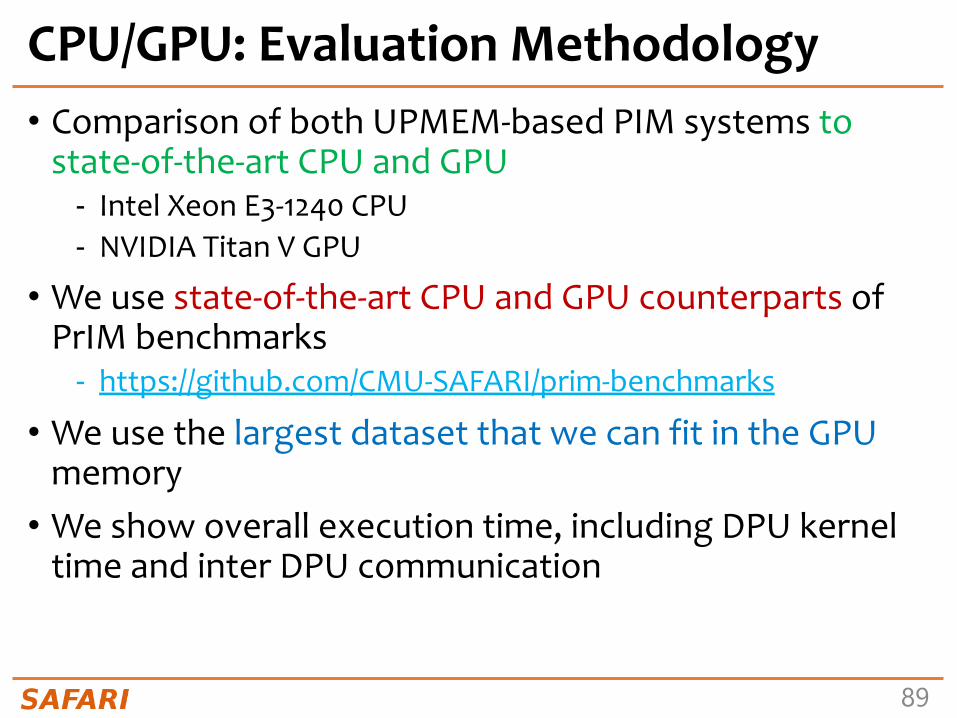
89
CPU/GPU: Evaluation Methodology• Comparison of both UPMEM-based PIM systems to
state-of-the-art CPU and GPU- Intel Xeon E3-1240 CPU- NVIDIA Titan V GPU
• We use state-of-the-art CPU and GPU counterparts of PrIM benchmarks- https://github.com/CMU-SAFARI/prim-benchmarks
• We use the largest dataset that we can fit in the GPUmemory• We show overall execution time, including DPU kernel
time and inter DPU communication
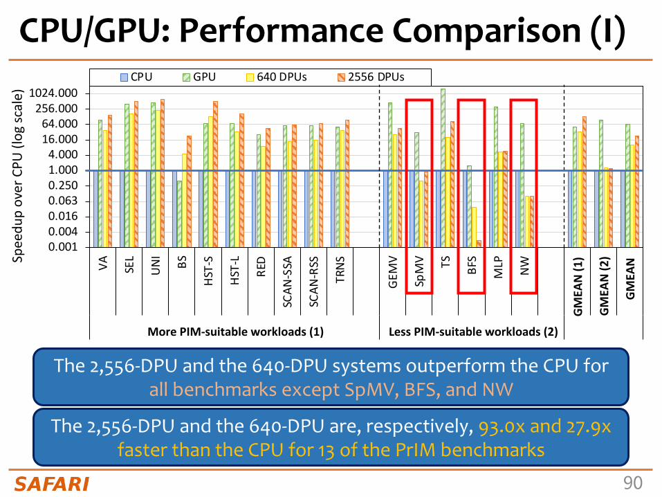
90
CPU/GPU: Performance Comparison (I)
0.0010.0040.0160.0630.2501.0004.000
16.00064.000
256.0001024.000
VA SEL
UN
I
BS
HST
-S
HST
-L
RED
SCAN
-SSA
SCAN
-RSS
TRN
S
GEM
V
SpM
V TS BFS
MLP NW
GM
EAN
(1)
GM
EAN
(2)
GM
EAN
More PIM-suitable workloads (1) Less PIM-suitable workloads (2)
Spee
dup
over
CPU
(log
scal
e)
CPU GPU 640 DPUs 2556 DPUs
GM
EAN
(1)
GM
EAN
(2)
GM
EAN
More PIM-suitable workloads (1) Less PIM-suitable workloads (2)
The 2,556-DPU and the 640-DPU systems outperform the CPU for all benchmarks except SpMV, BFS, and NW
The 2,556-DPU and the 640-DPU are, respectively, 93.0x and 27.9x faster than the CPU for 13 of the PrIM benchmarks

91
CPU/GPU: Performance Comparison (II)
0.0010.0040.0160.0630.2501.0004.000
16.00064.000
256.0001024.000
VA SEL
UN
I
BS
HST
-S
HST
-L
RED
SCAN
-SSA
SCAN
-RSS
TRN
S
GEM
V
SpM
V TS BFS
MLP NW
GM
EAN
(1)
GM
EAN
(2)
GM
EAN
More PIM-suitable workloads (1) Less PIM-suitable workloads (2)
Spee
dup
over
CPU
(log
scal
e)
CPU GPU 640 DPUs 2556 DPUs
GM
EAN
(1)
GM
EAN
(2)
GM
EAN
More PIM-suitable workloads (1) Less PIM-suitable workloads (2)
The 2,556-DPU outperforms the GPU for 10 PrIM benchmarks with an average of 2.54x
The performance of the 640-DPU is within 65% the performance of the GPU for the same 10 PrIM benchmarks

92
CPU/GPU: Performance Comparison (III)
0.0010.0040.0160.0630.2501.0004.000
16.00064.000
256.0001024.000
VA SEL
UN
I
BS
HST
-S
HST
-L
RED
SCAN
-SSA
SCAN
-RSS
TRN
S
GEM
V
SpM
V TS BFS
MLP NW
GM
EAN
(1)
GM
EAN
(2)
GM
EAN
More PIM-suitable workloads (1) Less PIM-suitable workloads (2)
Spee
dup
over
CPU
(log
scal
e)
CPU GPU 640 DPUs 2556 DPUs
GM
EAN
(1)
GM
EAN
(2)
GM
EAN
More PIM-suitable workloads (1) Less PIM-suitable workloads (2)
KEYOBSERVATION19TheUPMEM-basedPIMsystemcanoutperformastate-of-the-artGPUonworkloadswiththreekeycharacteristics:1. Streamingmemoryaccesses2. Noorlittleinter-DPUsynchronization3. Noorlittleuseofintegermultiplication,integerdivision,orfloating
pointoperationsThesethreekeycharacteristicsmakeaworkloadpotentiallysuitabletotheUPMEMPIMarchitecture.

93
CPU/GPU: Energy Comparison (I)
The 640-DPU system consumes on average 1.64x less energy than the CPU for all 16 PrIM benchmarks
For 12 benchmarks, the 640-DPU system provides energy savings of 5.23x over the CPU
0.030.060.130.250.501.002.004.008.00
16.0032.0064.00
128.00256.00
VA SEL
UN
I
BS
HST
-S
HST
-L
RED
SCAN
-SSA
SCAN
-RSS
TRN
S
GEM
V
SpM
V TS BFS
MLP NW
GM
EAN
(1)
GM
EAN
(2)
GM
EAN
More PIM-suitable workloads (1) Less PIM-suitable workloads (2)
Ener
gy sa
ving
s ove
r CPU
(log
scal
e)
CPU GPU 640 DPUs
GM
EAN
(1)
GM
EAN
(2)
GM
EAN
Less PIM-suitable workloads (2)More PIM-suitable workloads (1)

94
CPU/GPU: Energy Comparison (II)
0.030.060.130.250.501.002.004.008.00
16.0032.0064.00
128.00256.00
VA SEL
UN
I
BS
HST
-S
HST
-L
RED
SCAN
-SSA
SCAN
-RSS
TRN
S
GEM
V
SpM
V TS BFS
MLP NW
GM
EAN
(1)
GM
EAN
(2)
GM
EAN
More PIM-suitable workloads (1) Less PIM-suitable workloads (2)
Ener
gy sa
ving
s ove
r CPU
(log
scal
e)
CPU GPU 640 DPUs
GM
EAN
(1)
GM
EAN
(2)
GM
EAN
Less PIM-suitable workloads (2)More PIM-suitable workloads (1)
KEYOBSERVATION20TheUPMEM-basedPIMsystemprovideslargeenergysavingsoverastate-of-the-artCPU duetohigherperformance(thus,lowerstaticenergy)andlessdatamovementbetweenmemoryandprocessors.TheUPMEM-basedPIMsystemprovidesenergysavingsoverastate-of-the-artCPU/GPUonworkloadswhereitoutperformstheCPU/GPU.Thisisbecausethesourceofbothperformanceimprovementandenergysavingsisthesame:thesignificantreductionindatamovementbetweenthememoryandtheprocessorcores,whichtheUPMEM-basedPIMsystemcanprovideforPIM-suitableworkloads.
https://arxiv.org/pdf/2105.03814.pdfhttps://github.com/CMU-SAFARI/prim-benchmarks

95
Outline• Introduction
- Accelerator Model- UPMEM-based PIM System Overview
• UPMEM PIM Programming- Vector Addition- CPU-DPU Data Transfers- Inter-DPU Communication- CPU-DPU/DPU-CPU Transfer Bandwidth
• DRAM Processing Unit- Arithmetic Throughput- WRAM and MRAM Bandwidth
• PrIM Benchmarks- Roofline Model- Benchmark Diversity
• Evaluation- Strong and Weak Scaling- Comparison to CPU and GPU
• Key Takeaways

96
Key Takeaway 1
1234567891011121314151612345678910111213141516
1234567891011121314151612345678910111213141516 1
2345678910111213141516 12345678910111213141516
12345678910111213141516
12345678910111213141516
12345678910111213141516
123456789
10111213141516
123456789
10111213141516
123456789
10111213141516
123456789
10111213141516
123456789
10111213141516
123456789
10111213141516
0.030.060.130.250.501.002.004.008.00
16.0032.0064.00
1/4
096
1/2
048
1/1
024
1/5
12
1/2
56
1/1
28
1/6
4
1/3
2
1/1
6
1/8
1/4
1/21 2 4 8
Arith
met
ic T
hrou
ghpu
t (M
OPS
, log
scal
e)
Operational Intensity (OP/B)
(a) INT32, ADD (1 DPU)
21 84
Memory-bound region
Compute-bound region
The throughput saturation point is as low
as ¼ OP/B, i.e., 1 integer addition per
every 32-bit element fetched
KEYTAKEAWAY1TheUPMEMPIMarchitectureisfundamentallycomputebound.Asaresult,themostsuitableworkloadsarememory-bound.
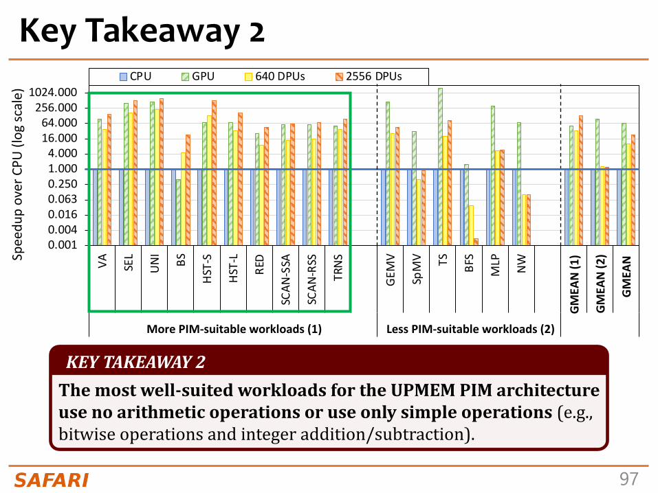
97
Key Takeaway 2
0.0010.0040.0160.0630.2501.0004.000
16.00064.000
256.0001024.000
VA SEL
UN
I
BS
HST
-S
HST
-L
RED
SCAN
-SSA
SCAN
-RSS
TRN
S
GEM
V
SpM
V TS BFS
MLP NW
GM
EAN
(1)
GM
EAN
(2)
GM
EAN
More PIM-suitable workloads (1) Less PIM-suitable workloads (2)
Spee
dup
over
CPU
(log
scal
e)
CPU GPU 640 DPUs 2556 DPUs
GM
EAN
(1)
GM
EAN
(2)
GM
EAN
More PIM-suitable workloads (1) Less PIM-suitable workloads (2)
KEYTAKEAWAY2Themostwell-suitedworkloadsfortheUPMEMPIMarchitectureusenoarithmeticoperationsoruseonlysimpleoperations (e.g.,bitwiseoperationsandintegeraddition/subtraction).

98
Key Takeaway 3
0.0010.0040.0160.0630.2501.0004.000
16.00064.000
256.0001024.000
VA SEL
UN
I
BS
HST
-S
HST
-L
RED
SCAN
-SSA
SCAN
-RSS
TRN
S
GEM
V
SpM
V TS BFS
MLP NW
GM
EAN
(1)
GM
EAN
(2)
GM
EAN
More PIM-suitable workloads (1) Less PIM-suitable workloads (2)
Spee
dup
over
CPU
(log
scal
e)
CPU GPU 640 DPUs 2556 DPUs
GM
EAN
(1)
GM
EAN
(2)
GM
EAN
More PIM-suitable workloads (1) Less PIM-suitable workloads (2)
KEYTAKEAWAY3Themostwell-suitedworkloadsfortheUPMEMPIMarchitecturerequirelittleornocommunicationacrossDPUs(inter-DPUcommunication).

99
Key Takeaway 4
KEYTAKEAWAY4•UPMEM-basedPIMsystemsoutperformstate-of-the-artCPUsintermsofperformanceandenergyefficiencyonmostofPrIMbenchmarks.
•UPMEM-basedPIMsystemsoutperformstate-of-the-artGPUsonamajorityofPrIM benchmarks,andtheoutlookisevenmorepositiveforfuturePIMsystems.
•UPMEM-basedPIMsystemsaremoreenergy-efficientthanstate-of-the-artCPUsandGPUsonworkloadsthattheyprovideperformanceimprovementsovertheCPUsandtheGPUs.
100
Executive Summary• Data movement between memory/storage units and compute units is a major
contributor to execution time and energy consumption• Processing-in-Memory (PIM) is a paradigm that can tackle the data movement
bottleneck- Though explored for +50 years, technology challenges prevented the successful materialization
• UPMEM has designed and fabricated the first publicly-available real-world PIM architecture- DDR4 chips embedding in-order multithreaded DRAM Processing Units (DPUs)
• Our work:- Introduction to UPMEM programming model and PIM architecture- Microbenchmark-based characterization of the DPU- Benchmarking and workload suitability study
• Main contributions:- Comprehensive characterization and analysis of the first commercially-available PIM architecture- PrIM (Processing-In-Memory) benchmarks:
• 16 workloads that are memory-bound in conventional processor-centric systems• Strong and weak scaling characteristics
- Comparison to state-of-the-art CPU and GPU
• Takeaways:- Workload characteristics for PIM suitability- Programming recommendations- Suggestions and hints for hardware and architecture designers of future PIM systems- PrIM: (a) programming samples, (b) evaluation and comparison of current and future PIM systems

101
PrIM Repository• All microbenchmarks, benchmarks, and scripts• https://github.com/CMU-SAFARI/prim-benchmarks

Juan Gómez Luna, Izzat El Hajj, Ivan Fernandez, Christina Giannoula,
Geraldo F. Oliveira, Onur Mutlu
Understanding a Modern Processing-in-Memory Architecture:Benchmarking and Experimental Characterization
https://arxiv.org/pdf/2105.03814.pdfhttps://github.com/CMU-SAFARI/prim-benchmarks

103
Technology Challenges
F. Devaux, "The true Processing In Memory accelerator," HotChips 2019. doi: 10.1109/HOTCHIPS.2019.8875680

104
CPU-DPU/DPU-CPU Transfers: 1 Rank (II)• CPU-DPU (serial/parallel/broadcast) and DPU-CPU (serial/parallel)• The number of DPUs varies between 1 and 64
0.27
0.12
6.68
4.74
16.88
0.060.130.250.501.002.004.008.00
16.00
1 2 4 8 16 32 64
Sust
aine
d CP
U-D
PU
Band
wid
th(G
B/s,
log
scal
e)
#DPUs
CPU-DPU (serial) DPU-CPU (serial)CPU-DPU (parallel) DPU-CPU (parallel)CPU-DPU (broadcast)
KEYOBSERVATION9ThesustainedbandwidthofparallelCPU-DPUtransfersishigherthanthesustainedbandwidthofparallelDPU-CPUtransfersduetodifferentimplementations ofCPU-DPUandDPU-CPUtransfersintheUPMEMruntimelibrary.
ThesustainedbandwidthofbroadcastCPU-DPUtransfers(i.e.,thesamebufferiscopiedtomultipleMRAMbanks)ishigherthanthatofparallelCPU-DPUtransfers (i.e.,differentbuffersarecopiedtodifferentMRAMbanks)duetohighertemporallocalityintheCPUcachehierarchy.

105
WRAM Bandwidth: ADD
𝑊𝑅𝐴𝑀 𝐵𝑎𝑛𝑑𝑤𝑖𝑑𝑡ℎ 𝑖𝑛𝐵𝑆
=𝐵𝑦𝑡𝑒𝑠 × 𝑓𝑟𝑒𝑞𝑢𝑒𝑛𝑐𝑦𝐷𝑃𝑈
#𝑖𝑛𝑠𝑡𝑟𝑢𝑐𝑡𝑖𝑜𝑛𝑠
2,818.98
1,682.46
42.0361.66
0
500
1000
1500
2000
2500
3000
1 2 3 4 5 6 7 8 9 10 11 12 13 14 15 16
Sust
aine
d W
RAM
Ba
ndw
idth
(MB/
s)
#Tasklets
STREAM (WRAM, INT64, 1DPU)COPYADDSCALETRIAD
ADD executes 5 instructions (2 ld, add, addc, sd).With 11 tasklets, 11 × 24 bytes in 55 cycles:
𝑊𝑅𝐴𝑀 𝐵𝑎𝑛𝑑𝑤𝑖𝑑𝑡ℎ 𝑖𝑛𝐵𝑆
= 1,680𝑀𝐵𝑠𝑎𝑡 350 𝑀𝐻𝑧

106
MRAM Read and Write Latency (IV)
MRAM latency changes slowly between 8 and 128 bytes
628.23
32
128
512
2048
1
10
100
10008 16 32 64 128
256
512
1024
2048
Late
ncy
(cyc
les)
Band
wid
th (M
B/s)
Data transfer size (bytes)
MRAM Read633.22
32
128
512
2048
1
10
100
1000
8 16 32 64 128
256
512
1024
2048
Late
ncy
(cyc
les)
Band
wid
th (M
B/s)
Data transfer size (bytes)
MRAM Write
For small transfers, the fixed cost (𝛼) dominates the variable cost (𝛽×𝑠𝑖𝑧𝑒)
PROGRAMMINGRECOMMENDATION2ForsmalltransfersbetweentheMRAMbankandtheWRAM,fetchmorebytesthannecessarywithina128-bytelimit.DoingsoincreasesthelikelihoodoffindingdatainWRAMforlateraccesses(i.e.,theprogramcancheckwhetherthedesireddataisinWRAMbeforeissuinganewMRAMaccess).

107
MRAM Read and Write Latency (V)
2,048-byte transfers are only 4% faster than 1,024-byte transfers
628.23
32
128
512
2048
1
10
100
10008 16 32 64 128
256
512
1024
2048
Late
ncy
(cyc
les)
Band
wid
th (M
B/s)
Data transfer size (bytes)
MRAM Read633.22
32
128
512
2048
1
10
100
1000
8 16 32 64 128
256
512
1024
2048
Late
ncy
(cyc
les)
Band
wid
th (M
B/s)
Data transfer size (bytes)
MRAM Write
Larger transfers require more WRAM, which may limit the number of tasklets
PROGRAMMINGRECOMMENDATION3ChoosethedatatransfersizebetweentheMRAMbankandtheWRAMbasedontheprogram’sWRAMusage,asitimposesatradeoffbetweenthesustainedMRAMbandwidthandthenumberoftasklets thatcanrunintheDPU(whichisdictatedbythelimitedWRAMcapacity).

108
0
10
20
30
40
50
60
0
50
100
150
200
250
300
1 4 16 64
Spee
dup
Exec
utio
n Ti
me
(ms)
#DPUsVA
DPU-CPUCPU-DPUInter-DPUDPUSpeedup
0
10
20
30
40
50
60
70
0
100
200
300
400
500
600
700
1 4 16 64
Spee
dup
Exec
utio
n Ti
me
(ms)
#DPUsGEMV
DPU-CPUCPU-DPUInter-DPUDPUSpeedup
0
5
10
15
20
25
30
35
40
0
100
200300
400
500
600700
800
9001000
1 4 16 64
Spee
dup
Exec
utio
n Ti
me
(ms)
#DPUsSpMV
DPU-CPUCPU-DPUInter-DPUDPUSpeedup
0
10
20
30
40
50
60
70
0
50
100
150
200
250
300
350
400
450
1 4 16 64
Spee
dup
Exec
utio
n Ti
me
(ms)
#DPUsSEL
DPU-CPUCPU-DPUInter-DPUDPUSpeedup
0
10
20
30
40
50
60
70
0
50
100
150
200
250
300
350
400
1 4 16 64
Spee
dup
Exec
utio
n Ti
me
(ms)
#DPUsUNI
DPU-CPUCPU-DPUInter-DPUDPUSpeedup
0
10
20
30
40
50
60
70
0
500
1000
1500
2000
2500
1 4 16 64
Spee
dup
Exec
utio
n Ti
me
(ms)
#DPUsBS
DPU-CPUCPU-DPUInter-DPUDPUSpeedup
0
10
20
30
40
50
60
70
0
2000
4000
6000
8000
10000
12000
1 4 16 64
Spee
dup
Exec
utio
n Ti
me
(ms)
#DPUsTS
DPU-CPUCPU-DPUInter-DPUDPUSpeedup
0
1
2
3
4
5
6
7
8
9
0
200
400
600
800
1000
1200
1400
1 4 16 64
Spee
dup
Exec
utio
n Ti
me
(ms)
#DPUsBFS
DPU-CPUCPU-DPUInter-DPUDPUSpeedup
0
10
20
30
40
50
60
70
0
200
400
600
800
1000
1200
1400
1 4 16 64
Spee
dup
Exec
utio
n Ti
me
(ms)
#DPUsMLP
DPU-CPUCPU-DPUInter-DPUDPUSpeedup
02
4
68
10
12
1416
18
20
0
500
1000
1500
2000
2500
1 4 16 64
Spee
dup
Exec
utio
n Ti
me
(ms)
#DPUsNW
DPU-CPUCPU-DPUInter-DPUDPUSpeedup
0
10
20
30
40
50
60
70
0
50
100
150
200
250
300
350
1 4 16 64
Spee
dup
Exec
utio
n Ti
me
(ms)
#DPUsRED
DPU-CPUCPU-DPUInter-DPUDPUSpeedup
0
10
20
30
40
50
60
70
0
100
200
300
400
500
600
700
800
1 4 16 64
Spee
dup
Exec
utio
n Ti
me
(ms)
#DPUsSCAN-SSA
DPU-CPU CPU-DPUInter-DPU DPU (Scan)DPU (Add) Speedup (Scan)Speedup (Add)
0
10
20
30
40
50
60
70
0.E+00
1.E+02
2.E+02
3.E+02
4.E+02
5.E+02
6.E+02
7.E+02
1 4 16 64
Spee
dup
Exec
utio
n Ti
me
(ms)
#DPUsSCAN-RSS
DPU-CPU CPU-DPUInter-DPU DPU (Scan)DPU (Reduce) Speedup (Scan)Speedup (Red.)
0
10
20
30
40
50
60
70
0.E+00
1.E+05
2.E+05
3.E+05
4.E+05
5.E+05
6.E+05
7.E+05
8.E+05
1 4 16 64
Spee
dup
Exec
utio
n Ti
me
(ms)
#DPUsTRNS
DPU-CPU CPU-DPU (Step 1)Inter-DPU DPU (Step 3)DPU (Step 2) Speedup (Step 3)Speedup (Step 2)
0
10
20
30
40
50
60
0
20
40
60
80
100
120
140
160
1 4
16 64
Spee
dup
Exec
utio
n Ti
me
(ms)
#DPUsHST-S
DPU-CPUCPU-DPUInter-DPUDPUSpeedup
0
10
20
30
40
50
60
70
050
100
150200
250
300
350400
450
500
1 4 16 64
Spee
dup
Exec
utio
n Ti
me
(ms)
#DPUsHST-L
DPU-CPUCPU-DPUInter-DPUDPUSpeedup
Strong Scaling: 1 Rank (IV)VA, GEMV, TS, MLP, HST-S, HST-L, RED, SCAN-SSA, SCAN-RSS, TRNS use parallel transfers.CPU-DPU and DPU-CPU transfer times decrease as we increase the number of DPUs
BS, NW use parallel transfers but do not reduce transfer times:- BS transfers a complete array
to all DPUs.- NW does not use all DPUs in all
iterations
SpMV, SEL, UNI, BFS cannot use parallel transfers, as the transfer size per DPU is not fixed
PROGRAMMINGRECOMMENDATION5ParallelCPU-DPU/DPU-CPUtransfersinsidearankofDPUsarerecommendedforreal-worldworkloadswhenalltransferredbuffersareofthesamesize.

109
• Strong scaling experiments on 32 rank- We set the number
of tasklets to the best performing one
- The number of DPUs is 256, 512, 1024, 2048
- We show the breakdown of execution time:• DPU: Execution
time on the DPU• Inter-DPU: Time for
inter-DPU communication via the host CPU
• We do not show CPU-DPU/DPU-CPU transfer times
- Speedup over 256 DPUs
0
1
2
3
4
5
6
7
8
0102030405060708090
256
512
1024
2048
Spee
dup
Exec
utio
n Ti
me
(ms)
#DPUs
VA
Inter-DPUDPUSpeedup
0
1
2
3
4
5
6
7
8
0
20
40
60
80
100
120
140
160
256
512
1024
2048
Spee
dup
Exec
utio
n Ti
me
(ms)
#DPUs
GEMV
Inter-DPUDPUSpeedup
0
1
2
3
4
5
6
7
0100200300400500600700800900
1000
256
512
1024
2048
Spee
dup
Exec
utio
n Ti
me
(ms)
#DPUs
SpMV
Inter-DPUDPUSpeedup
0123456789
0
20
40
60
80
100
120
140
160
256
512
1024
2048
Spee
dup
Exec
utio
n Ti
me
(ms)
#DPUs
SEL
Inter-DPUDPUSpeedup
0
1
2
3
4
5
6
7
8
0
20
40
60
80
100
120
256
512
1024
2048
Spee
dup
Exec
utio
n Ti
me
(ms)
#DPUs
UNI
Inter-DPUDPUSpeedup
0.01.02.03.04.05.06.07.08.09.0
0
100
200
300
400
500
600
700
256
512
1024
2048
Spee
dup
Exec
utio
n Ti
me
(ms)
#DPUs
BS
Inter-DPUDPUSpeedup
0.01.02.03.04.05.06.07.08.09.0
0
500
1000
1500
2000
2500
3000
256
512
1024
2048
Spee
dup
Exec
utio
n Ti
me
(ms)
#DPUs
TS
Inter-DPUDPUSpeedup
0
1
1
2
2
3
0100020003000400050006000700080009000
256
512
1024
2048
Spee
dup
Exec
utio
n Ti
me
(ms)
#DPUs
BFS
Inter-DPUDPUSpeedup
0
1
2
3
4
5
6
7
8
0
200
400
600
800
1000
1200
256
512
1024
2048
Spee
dup
Exec
utio
n Ti
me
(ms)
#DPUs
MLP
Inter-DPUDPUSpeedup
0.0
0.5
1.0
1.5
2.0
2.5
0100002000030000400005000060000700008000090000
100000
256
512
1024
2048
Spee
dup
Exec
utio
n Ti
me
(ms)
#DPUs
NW
Inter-DPUDPUSpeedup
0
1
2
3
4
5
6
7
8
0
5
10
15
20
25
30
35
40
256
512
1024
2048
Spee
dup
Exec
utio
n Ti
me
(ms)
#DPUs
HST-S
Inter-DPUDPUSpeedup
0
1
2
3
4
5
6
7
8
9
0
20
40
60
80
100
120
256
512
1024
2048
Spee
dup
Exec
utio
n Ti
me
(ms)
#DPUs
HST-L
Inter-DPUDPUSpeedup
0
1
2
3
4
5
6
7
8
0
20
40
60
80
100
120
140
160
180
256
512
1024
2048
Spee
dup
Exec
utio
n Ti
me
(ms)
#DPUs
RED
Inter-DPUDPUSpeedup
0
2
4
6
8
10
12
0
50
100
150
200
250
300
350
400
256
512
1024
2048
Spee
dup
Exec
utio
n Ti
me
(ms)
#DPUs
SCAN-SSA
Inter-DPUDPU (Scan)DPU (Add)Speedup (Scan)Speedup (Add)
0
2
4
6
8
10
12
0
50
100
150
200
250
300
350
256
512
1024
2048
Spee
dup
Exec
utio
n Ti
me
(ms)
#DPUs
SCAN-RSS
Inter-DPUDPU (Scan)DPU (Reduce)Speedup (Scan)Speedup (Red.)
0
1
2
3
4
5
6
7
8
9
0
500
1000
1500
2000
2500
3000
3500
256
512
1024
2048
Spee
dup
Exec
utio
n Ti
me
(ms)
#DPUs
TRNS
Inter-DPUDPU (Step 3)DPU (Step 2)Speedup (Step 3)Speedup (Step 2)
Strong Scaling: 32 Ranks (I)
0
1
2
3
4
5
6
7
8
0
200
400
600
800
1000
1200
256
512
1024
2048
Spee
dup
Exec
utio
n Ti
me
(ms)
#DPUs
MLP
Inter-DPUDPUSpeedup

110
0
1
2
3
4
5
6
7
8
0102030405060708090
256
512
1024
2048
Spee
dup
Exec
utio
n Ti
me
(ms)
#DPUs
VA
Inter-DPUDPUSpeedup
0
1
2
3
4
5
6
7
8
0
20
40
60
80
100
120
140
160
256
512
1024
2048
Spee
dup
Exec
utio
n Ti
me
(ms)
#DPUs
GEMV
Inter-DPUDPUSpeedup
0
1
2
3
4
5
6
7
0100200300400500600700800900
1000
256
512
1024
2048
Spee
dup
Exec
utio
n Ti
me
(ms)
#DPUs
SpMV
Inter-DPUDPUSpeedup
0123456789
0
20
40
60
80
100
120
140
160
256
512
1024
2048
Spee
dup
Exec
utio
n Ti
me
(ms)
#DPUs
SEL
Inter-DPUDPUSpeedup
0
1
2
3
4
5
6
7
8
0
20
40
60
80
100
120
256
512
1024
2048
Spee
dup
Exec
utio
n Ti
me
(ms)
#DPUs
UNI
Inter-DPUDPUSpeedup
0.01.02.03.04.05.06.07.08.09.0
0
100
200
300
400
500
600
700
256
512
1024
2048
Spee
dup
Exec
utio
n Ti
me
(ms)
#DPUs
BS
Inter-DPUDPUSpeedup
0.01.02.03.04.05.06.07.08.09.0
0
500
1000
1500
2000
2500
3000
256
512
1024
2048
Spee
dup
Exec
utio
n Ti
me
(ms)
#DPUs
TS
Inter-DPUDPUSpeedup
0
1
1
2
2
3
0100020003000400050006000700080009000
256
512
1024
2048
Spee
dup
Exec
utio
n Ti
me
(ms)
#DPUs
BFS
Inter-DPUDPUSpeedup
0
1
2
3
4
5
6
7
8
0
200
400
600
800
1000
1200
256
512
1024
2048
Spee
dup
Exec
utio
n Ti
me
(ms)
#DPUs
MLP
Inter-DPUDPUSpeedup
0.0
0.5
1.0
1.5
2.0
2.5
0100002000030000400005000060000700008000090000
100000
256
512
1024
2048
Spee
dup
Exec
utio
n Ti
me
(ms)
#DPUs
NW
Inter-DPUDPUSpeedup
0
1
2
3
4
5
6
7
8
0
5
10
15
20
25
30
35
40
256
512
1024
2048
Spee
dup
Exec
utio
n Ti
me
(ms)
#DPUs
HST-S
Inter-DPUDPUSpeedup
0
1
2
3
4
5
6
7
8
9
0
20
40
60
80
100
120
256
512
1024
2048
Spee
dup
Exec
utio
n Ti
me
(ms)
#DPUs
HST-L
Inter-DPUDPUSpeedup
0
1
2
3
4
5
6
7
8
0
20
40
60
80
100
120
140
160
180
256
512
1024
2048
Spee
dup
Exec
utio
n Ti
me
(ms)
#DPUs
RED
Inter-DPUDPUSpeedup
0
2
4
6
8
10
12
0
50
100
150
200
250
300
350
400
256
512
1024
2048
Spee
dup
Exec
utio
n Ti
me
(ms)
#DPUs
SCAN-SSA
Inter-DPUDPU (Scan)DPU (Add)Speedup (Scan)Speedup (Add)
0
2
4
6
8
10
12
0
50
100
150
200
250
300
350
256
512
1024
2048
Spee
dup
Exec
utio
n Ti
me
(ms)
#DPUs
SCAN-RSS
Inter-DPUDPU (Scan)DPU (Reduce)Speedup (Scan)Speedup (Red.)
0
1
2
3
4
5
6
7
8
9
0
500
1000
1500
2000
2500
3000
3500
256
512
1024
2048
Spee
dup
Exec
utio
n Ti
me
(ms)
#DPUs
TRNS
Inter-DPUDPU (Step 3)DPU (Step 2)Speedup (Step 3)Speedup (Step 2)
Strong Scaling: 32 Ranks (II)
SpMV, BFS, NW do not scale linearly due to load imbalance
KEYOBSERVATION14LoadbalancingacrossDPUsensureslinearreductionoftheexecutiontimespentontheDPUs foragivenproblemsize,whenallavailableDPUsareused(asobservedinstrongscalingexperiments).
VA, GEMV, SEL, UNI, BS, TS, MLP, HST-S, HSTS-L, RED, SCAN-SSA (both kernel), SCAN-RSS (both kernels), and TRNS (both kernels) scale linearly with the number of DPUs

111
0
1
2
3
4
5
6
7
8
0102030405060708090
256
512
1024
2048
Spee
dup
Exec
utio
n Ti
me
(ms)
#DPUs
VA
Inter-DPUDPUSpeedup
0
1
2
3
4
5
6
7
8
0
20
40
60
80
100
120
140
160
256
512
1024
2048
Spee
dup
Exec
utio
n Ti
me
(ms)
#DPUs
GEMV
Inter-DPUDPUSpeedup
0
1
2
3
4
5
6
7
0100200300400500600700800900
1000
256
512
1024
2048
Spee
dup
Exec
utio
n Ti
me
(ms)
#DPUs
SpMV
Inter-DPUDPUSpeedup
0123456789
0
20
40
60
80
100
120
140
160
256
512
1024
2048
Spee
dup
Exec
utio
n Ti
me
(ms)
#DPUs
SEL
Inter-DPUDPUSpeedup
0
1
2
3
4
5
6
7
8
0
20
40
60
80
100
120
256
512
1024
2048
Spee
dup
Exec
utio
n Ti
me
(ms)
#DPUs
UNI
Inter-DPUDPUSpeedup
0.01.02.03.04.05.06.07.08.09.0
0
100
200
300
400
500
600
700
256
512
1024
2048
Spee
dup
Exec
utio
n Ti
me
(ms)
#DPUs
BS
Inter-DPUDPUSpeedup
0.01.02.03.04.05.06.07.08.09.0
0
500
1000
1500
2000
2500
3000
256
512
1024
2048
Spee
dup
Exec
utio
n Ti
me
(ms)
#DPUs
TS
Inter-DPUDPUSpeedup
0
1
1
2
2
3
0100020003000400050006000700080009000
256
512
1024
2048
Spee
dup
Exec
utio
n Ti
me
(ms)
#DPUs
BFS
Inter-DPUDPUSpeedup
0
1
2
3
4
5
6
7
8
0
200
400
600
800
1000
1200
256
512
1024
2048
Spee
dup
Exec
utio
n Ti
me
(ms)
#DPUs
MLP
Inter-DPUDPUSpeedup
0.0
0.5
1.0
1.5
2.0
2.5
0100002000030000400005000060000700008000090000
100000
256
512
1024
2048
Spee
dup
Exec
utio
n Ti
me
(ms)
#DPUs
NW
Inter-DPUDPUSpeedup
0
1
2
3
4
5
6
7
8
0
5
10
15
20
25
30
35
40
256
512
1024
2048
Spee
dup
Exec
utio
n Ti
me
(ms)
#DPUs
HST-S
Inter-DPUDPUSpeedup
0
1
2
3
4
5
6
7
8
9
0
20
40
60
80
100
120
256
512
1024
2048
Spee
dup
Exec
utio
n Ti
me
(ms)
#DPUs
HST-L
Inter-DPUDPUSpeedup
0
1
2
3
4
5
6
7
8
0
20
40
60
80
100
120
140
160
180
256
512
1024
2048
Spee
dup
Exec
utio
n Ti
me
(ms)
#DPUs
RED
Inter-DPUDPUSpeedup
0
2
4
6
8
10
12
0
50
100
150
200
250
300
350
400
256
512
1024
2048
Spee
dup
Exec
utio
n Ti
me
(ms)
#DPUs
SCAN-SSA
Inter-DPUDPU (Scan)DPU (Add)Speedup (Scan)Speedup (Add)
0
2
4
6
8
10
12
0
50
100
150
200
250
300
350
256
512
1024
2048
Spee
dup
Exec
utio
n Ti
me
(ms)
#DPUs
SCAN-RSS
Inter-DPUDPU (Scan)DPU (Reduce)Speedup (Scan)Speedup (Red.)
0
1
2
3
4
5
6
7
8
9
0
500
1000
1500
2000
2500
3000
3500
256
512
1024
2048
Spee
dup
Exec
utio
n Ti
me
(ms)
#DPUs
TRNS
Inter-DPUDPU (Step 3)DPU (Step 2)Speedup (Step 3)Speedup (Step 2)
Strong Scaling: 32 Ranks (III)
KEYOBSERVATION15TheoverheadofmergingpartialresultsfromDPUsinthehostCPUistolerableacrossallPrIM benchmarksthatneedit.
SEL, UNI, HST-S, HST-L, RED only need to merge final results
KEYOBSERVATION16ComplexsynchronizationacrossDPUs(i.e.,inter-DPUsynchronizationinvolvingtwo-waycommunicationwiththehostCPU)imposessignificantoverhead,whichlimitsscalabilitytomoreDPUs.
BFS, MLP, NW, SCAN-SSA, SCAN-RSS have more complex communication

112
Weak Scaling: 1 Rank
KEYOBSERVATION17Equally-sizedproblemsassignedtodifferentDPUsandlittle/nointer-DPUsynchronizationleadtolinearweakscalingoftheexecutiontimespentontheDPUs(i.e.,constantexecutiontimewhenweincreasethenumberofDPUsandthedatasetsizeaccordingly).
KEYOBSERVATION18SustainedbandwidthofparallelCPU-DPU/DPU-CPUtransfersinsidearankofDPUsincreasessublinearlywiththenumberofDPUs.
0
100
200
300
400
500
600
700
1 4 16 64
Exec
utio
n Ti
me
(ms)
#DPUsVA
DPU-CPUCPU-DPUInter-DPUDPU
0
50
100
150
200
250
300
350
1 4 16 64
Exec
utio
n Ti
me
(ms)
#DPUsGEMV
DPU-CPUCPU-DPUInter-DPUDPU
0
500
1000
1500
2000
2500
3000
3500
1 4 16 64
Exec
utio
n Ti
me
(ms)
#DPUsSpMV
DPU-CPUCPU-DPUInter-DPUDPU
0
1000
20003000
4000
5000
60007000
8000
900010000
1 4 16 64
Exec
utio
n Ti
me
(ms)
#DPUsSEL
DPU-CPUCPU-DPUInter-DPUDPU
0
10002000
3000
40005000
6000
7000
80009000
10000
1 4 16 64
Exec
utio
n Ti
me
(ms)
#DPUsUNI
DPU-CPUCPU-DPUInter-DPUDPU
0
500
1000
1500
2000
2500
3000
1 4 16 64
Exec
utio
n Ti
me
(ms)
#DPUsBS
DPU-CPUCPU-DPUInter-DPUDPU
0
2000
4000
6000
8000
10000
12000
1 4 16 64
Exec
utio
n Ti
me
(ms)
#DPUsTS
DPU-CPUCPU-DPUInter-DPUDPU
0
2000
4000
6000
8000
10000
12000
14000
1 4 16 64
Exec
utio
n Ti
me
(ms)
#DPUsBFS
DPU-CPUCPU-DPUInter-DPUDPU
0
50
100
150
200
250
300
350
400
450
1 4 16 64
Exec
utio
n Ti
me
(ms)
#DPUsMLP
DPU-CPUCPU-DPUInter-DPUDPU
02000
4000
60008000
10000
12000
1400016000
18000
20000
1 4 16 64
Exec
utio
n Ti
me
(ms)
#DPUsNW
DPU-CPUCPU-DPUInter-DPUDPU
0
50
100
150
200
250
1 4
16 64
Exec
utio
n Ti
me
(ms)
#DPUsHST-S
DPU-CPUCPU-DPUInter-DPUDPU
0
100
200
300
400
500
600
1 4 16 64
Exec
utio
n Ti
me
(ms)
#DPUsHST-L
DPU-CPUCPU-DPUInter-DPUDPU
0
100
200
300
400
500
600
700
1 4 16 64
Exec
utio
n Ti
me
(ms)
#DPUsRED
DPU-CPUCPU-DPUInter-DPUDPU
0
200
400
600
800
1000
1200
1400
1600
1 4 16 64
Exec
utio
n Ti
me
(ms)
#DPUsSCAN-SSA
DPU-CPUCPU-DPUInter-DPUDPU (Scan)DPU (Add)
0
200
400
600
800
1000
1200
1 4 16 64
Exec
utio
n Ti
me
(ms)
#DPUsSCAN-RSS
DPU-CPUCPU-DPUInter-DPUDPU (Scan)DPU (Reduce)
0
2000
4000
6000
8000
10000
12000
14000
16000
180001 4 16 64
Exec
utio
n Ti
me
(ms)
#DPUsTRNS
DPU-CPUCPU-DPU (Step 1)Inter-DPUDPU (Step 3)DPU (Step 2)
0
100
200
300
400
500
600
700
1 4 16 64
Exec
utio
n Ti
me
(ms)
#DPUsVA
DPU-CPUCPU-DPUInter-DPUDPU

113
Resources• UPMEM SDK documentation
- https://sdk.upmem.com/master/00_ToolchainAtAGlance.html
• Fabrice Devaux’s presentation at HotChips 2019- https://ieeexplore.ieee.org/stamp/stamp.jsp?tp=&arnumber=8
875680
• Onur’s lectures and talks

114
Characterization of UPMEM PIM• Microbenchmarks
- Pipeline throughput- STREAM benchmark: WRAM, MRAM- Strided accesses and GUPS- Throughput vs. Operational intensity- CPU-DPU data transfers
• Real-world benchmarks- Dense linear algebra- Sparse linear algebra- Databases- Graph processing- Bioinformatics- Etc.
115
Banner Colors
This is a question or an observation
This is an answer from, e.g., UPMEM
documentation or our own research
This is an idea or a discussion starter, an
opportunity for brainstorming

116
DPU Sharing? Security Implications?• DPUs cannot be shared across multiple CPU processes
- There are so many DPUs in the system that there is no need for sharing
• According to UPMEM, this assumption makes things simpler- No need for OS- Simplified security implications: No side channels
Is it possible to perform RowHammer bit flips?Can we attack the previous or the next application
that runs on a DPU?
RowHammer patents and Giray’s paper?

117
More Questions and Ideas?How do we handle memory coherence,
memory oversubscription, etc.?
They are programmer’s responsibility
A software library to handle memory management transparently to programmers
ASPLOS 2010

118
Arithmetic Throughput (II)
Huge throughput difference between add/sub and mul/div
DPUs do not have a 32-bit multiplier.mul/div implementation is based on bit shifting and addition:
maximum of 32 cycles (instructions) to complete
0
1
2
3
4
5
6
1 3 5 7 9 11 13 15 17 19 21 23
Arith
met
ic T
hrou
ghpu
t (M
OPS
)
#Tasklets
(d) DOUBLE (1 DPU) ADDSUBMULDIV
0
1
2
3
4
5
6
1 3 5 7 9 11 13 15 17 19 21 23
Arith
met
ic T
hrou
ghpu
t (M
OPS
)
#Tasklets
(c) FLOAT (1 DPU)
ADDSUBMULDIV
0
10
20
30
40
50
60
70
1 3 5 7 9 11 13 15 17 19 21 23
Arith
met
ic T
hrou
ghpu
t (M
OPS
)
#Tasklets
(b) INT64 (1 DPU)
ADDSUBMULDIV
0
10
20
30
40
50
60
70
1 3 5 7 9 11 13 15 17 19 21 23
Arith
met
ic T
hrou
ghpu
t (M
OPS
)
#Tasklets
(a) INT32 (1 DPU)
ADDSUBMULDIV
There is an 8-bit multiplier in the pipeline.Would it be possible to use it for more efficient implementation?
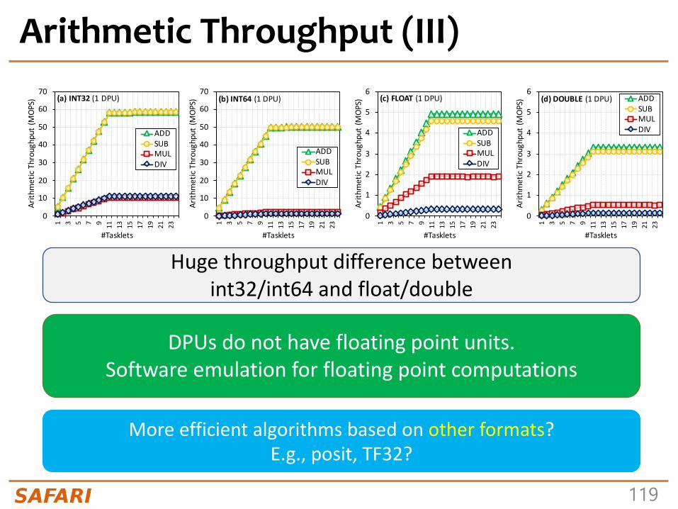
119
Arithmetic Throughput (III)
Huge throughput difference between int32/int64 and float/double
DPUs do not have floating point units.Software emulation for floating point computations
0
1
2
3
4
5
6
1 3 5 7 9 11 13 15 17 19 21 23
Arith
met
ic T
hrou
ghpu
t (M
OPS
)
#Tasklets
(d) DOUBLE (1 DPU) ADDSUBMULDIV
0
1
2
3
4
5
6
1 3 5 7 9 11 13 15 17 19 21 23
Arith
met
ic T
hrou
ghpu
t (M
OPS
)
#Tasklets
(c) FLOAT (1 DPU)
ADDSUBMULDIV
0
10
20
30
40
50
60
70
1 3 5 7 9 11 13 15 17 19 21 23
Arith
met
ic T
hrou
ghpu
t (M
OPS
)
#Tasklets
(b) INT64 (1 DPU)
ADDSUBMULDIV
0
10
20
30
40
50
60
70
1 3 5 7 9 11 13 15 17 19 21 23
Arith
met
ic T
hrou
ghpu
t (M
OPS
)
#Tasklets
(a) INT32 (1 DPU)
ADDSUBMULDIV
More efficient algorithms based on other formats? E.g., posit, TF32?
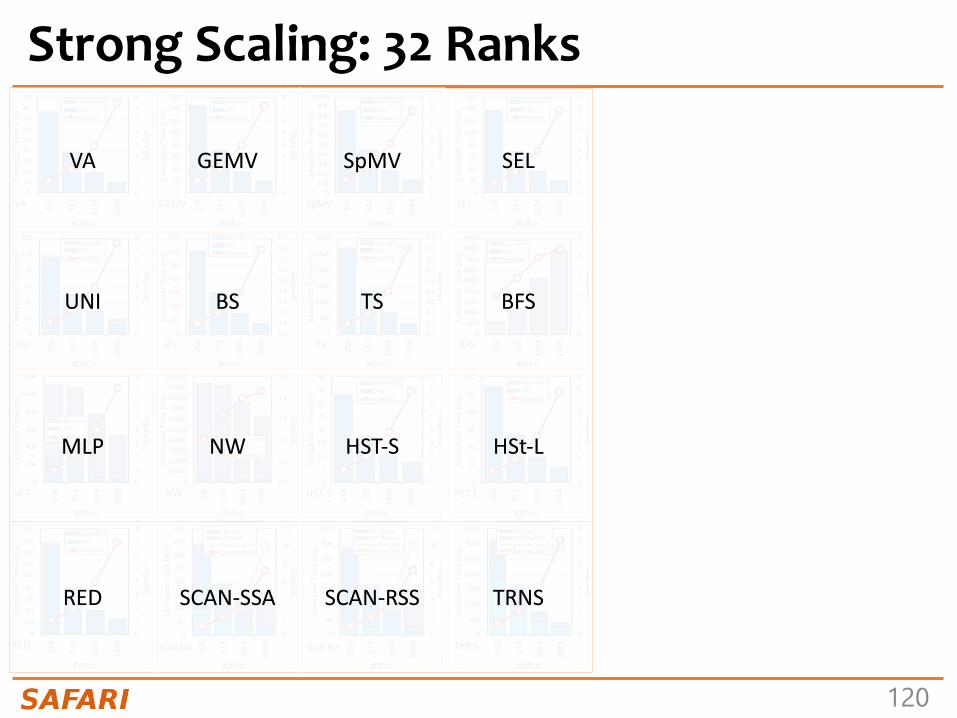
120
0
1
2
3
4
5
6
7
8
0102030405060708090
256
512
1024
2048
Spee
dup
Exec
utio
n Ti
me
(ms)
#DPUs
VA
Inter-DPUDPUSpeedup
0
1
2
3
4
5
6
7
8
0
20
40
60
80
100
120
140
160
256
512
1024
2048
Spee
dup
Exec
utio
n Ti
me
(ms)
#DPUs
GEMV
Inter-DPUDPUSpeedup
0
1
2
3
4
5
6
7
0100200300400500600700800900
1000
256
512
1024
2048
Spee
dup
Exec
utio
n Ti
me
(ms)
#DPUs
SpMV
Inter-DPUDPUSpeedup
0123456789
0
20
40
60
80
100
120
140
160
256
512
1024
2048
Spee
dup
Exec
utio
n Ti
me
(ms)
#DPUs
SEL
Inter-DPUDPUSpeedup
0
1
2
3
4
5
6
7
8
0
20
40
60
80
100
120
256
512
1024
2048
Spee
dup
Exec
utio
n Ti
me
(ms)
#DPUs
UNI
Inter-DPUDPUSpeedup
0.01.02.03.04.05.06.07.08.09.0
0
100
200
300
400
500
600
700
256
512
1024
2048
Spee
dup
Exec
utio
n Ti
me
(ms)
#DPUs
BS
Inter-DPUDPUSpeedup
0.01.02.03.04.05.06.07.08.09.0
0
500
1000
1500
2000
2500
3000
256
512
1024
2048
Spee
dup
Exec
utio
n Ti
me
(ms)
#DPUs
TS
Inter-DPUDPUSpeedup
0
1
1
2
2
3
0100020003000400050006000700080009000
256
512
1024
2048
Spee
dup
Exec
utio
n Ti
me
(ms)
#DPUs
BFS
Inter-DPUDPUSpeedup
0
1
2
3
4
5
6
7
8
0
200
400
600
800
1000
1200
256
512
1024
2048
Spee
dup
Exec
utio
n Ti
me
(ms)
#DPUs
MLP
Inter-DPUDPUSpeedup
0.0
0.5
1.0
1.5
2.0
2.5
0100002000030000400005000060000700008000090000
100000
256
512
1024
2048
Spee
dup
Exec
utio
n Ti
me
(ms)
#DPUs
NW
Inter-DPUDPUSpeedup
0
1
2
3
4
5
6
7
8
0
5
10
15
20
25
30
35
40
256
512
1024
2048
Spee
dup
Exec
utio
n Ti
me
(ms)
#DPUs
HST-S
Inter-DPUDPUSpeedup
0
1
2
3
4
5
6
7
8
9
0
20
40
60
80
100
120
256
512
1024
2048
Spee
dup
Exec
utio
n Ti
me
(ms)
#DPUs
HST-L
Inter-DPUDPUSpeedup
0
1
2
3
4
5
6
7
8
0
20
40
60
80
100
120
140
160
180
256
512
1024
2048
Spee
dup
Exec
utio
n Ti
me
(ms)
#DPUs
RED
Inter-DPUDPUSpeedup
0
2
4
6
8
10
12
0
50
100
150
200
250
300
350
400
256
512
1024
2048
Spee
dup
Exec
utio
n Ti
me
(ms)
#DPUs
SCAN-SSA
Inter-DPUDPU (Scan)DPU (Add)Speedup (Scan)Speedup (Add)
0
2
4
6
8
10
12
0
50
100
150
200
250
300
350
256
512
1024
2048
Spee
dup
Exec
utio
n Ti
me
(ms)
#DPUs
SCAN-RSS
Inter-DPUDPU (Scan)DPU (Reduce)Speedup (Scan)Speedup (Red.)
0
1
2
3
4
5
6
7
8
9
0
500
1000
1500
2000
2500
3000
3500
256
512
1024
2048
Spee
dup
Exec
utio
n Ti
me
(ms)
#DPUs
TRNS
Inter-DPUDPU (Step 3)DPU (Step 2)Speedup (Step 3)Speedup (Step 2)
VA GEMV SpMV SEL
UNI TS BFSBS
MLP HST-S HSt-LNW
RED SCAN-RSS TRNSSCAN-SSA
Strong Scaling: 32 Ranks
VA GEMV SpMV SEL
UNI TS BFSBS
MLP HST-S HSt-LNW
RED SCAN-RSS TRNSSCAN-SSA

121
Strong Scaling: 1 Rank
0
10
20
30
40
50
60
0
50
100
150
200
250
300
1 4 16 64
Spee
dup
Exec
utio
n Ti
me
(ms)
#DPUsVA
DPU-CPUCPU-DPUInter-DPUDPUSpeedup
0
10
20
30
40
50
60
70
0
200
400
600
800
1000
1200
1400
1600
1800
1 4 16 64
Spee
dup
Exec
utio
n Ti
me
(ms)
#DPUsGEMV
DPU-CPUCPU-DPUInter-DPUDPUSpeedup
0
5
10
15
20
25
30
35
40
0
100
200300
400
500
600700
800
9001000
1 4 16 64
Spee
dup
Exec
utio
n Ti
me
(ms)
#DPUsSpMV
DPU-CPUCPU-DPUInter-DPUDPUSpeedup
0
10
20
30
40
50
60
70
0
50
100
150
200
250
300
350
400
450
1 4 16 64
Spee
dup
Exec
utio
n Ti
me
(ms)
#DPUsSEL
DPU-CPUCPU-DPUInter-DPUDPUSpeedup
0
10
20
30
40
50
60
70
0
50
100
150
200
250
300
350
4001 4 16 64
Spee
dup
Exec
utio
n Ti
me
(ms)
#DPUsUNI
DPU-CPUCPU-DPUInter-DPUDPUSpeedup
0
5
10
15
20
25
30
0
200
400
600
800
1000
1200
1 4 16 64
Spee
dup
Exec
utio
n Ti
me
(ms)
#DPUsBS
DPU-CPUCPU-DPUInter-DPUDPUSpeedup
0
10
20
30
40
50
60
70
0
2000
4000
6000
8000
10000
12000
1 4 16 64
Spee
dup
Exec
utio
n Ti
me
(ms)
#DPUsTS
DPU-CPUCPU-DPUInter-DPUDPUSpeedup
0
1
2
3
4
5
6
7
8
9
0
200
400
600
800
1000
1200
1400
1 4 16 64
Spee
dup
Exec
utio
n Ti
me
(ms)
#DPUsBFS
DPU-CPUCPU-DPUInter-DPUDPUSpeedup
0
10
20
30
40
50
60
70
0
200
400
600
800
1000
1200
1400
1600
1800
1 4 16 64
Spee
dup
Exec
utio
n Ti
me
(ms)
#DPUsMLP
DPU-CPUCPU-DPUInter-DPUDPUSpeedup
0
2
4
6
8
10
12
14
0200
400
600800
1000
1200
14001600
1800
20001 4 16 64
Spee
dup
Exec
utio
n Ti
me
(ms)
#DPUsNW
DPU-CPUCPU-DPUInter-DPUDPUSpeedup
0
10
20
30
40
50
60
70
0
50
100
150
200
250
300
350
1 4 16 64
Spee
dup
Exec
utio
n Ti
me
(ms)
#DPUsRED
DPU-CPUCPU-DPUInter-DPUDPUSpeedup
0
10
20
30
40
50
60
70
0
100
200
300
400
500
600
700
800
1 4 16 64
Spee
dup
Exec
utio
n Ti
me
(ms)
#DPUsSCAN-SSA
DPU-CPU CPU-DPUInter-DPU DPU (Scan)DPU (Add) Speedup (Scan)Speedup (Add)
0
10
20
30
40
50
60
70
0.E+00
1.E+02
2.E+02
3.E+02
4.E+02
5.E+02
6.E+02
7.E+021 4 16 64
Spee
dup
Exec
utio
n Ti
me
(ms)
#DPUsSCAN-RSS
DPU-CPU CPU-DPUInter-DPU DPU (Scan)DPU (Reduce) Speedup (Scan)Speedup (Red.)
0
10
20
30
40
50
60
70
0.E+00
1.E+05
2.E+05
3.E+05
4.E+05
5.E+05
6.E+05
7.E+05
8.E+05
1 4 16 64
Spee
dup
Exec
utio
n Ti
me
(ms)
#DPUsTRNS
DPU-CPU CPU-DPU (Step 1)Inter-DPU DPU (Step 3)DPU (Step 2) Speedup (Step 3)Speedup (Step 2)
0
10
20
30
40
50
60
0
20
40
60
80
100
120
140
160
1 4
16 64
Spee
dup
Exec
utio
n Ti
me
(ms)
#DPUsHST-S
DPU-CPUCPU-DPUInter-DPUDPUSpeedup
0
10
20
30
40
50
60
70
050
100
150200
250
300
350400
450
500
1 4 16 64
Spee
dup
Exec
utio
n Ti
me
(ms)
#DPUsHST-L
DPU-CPUCPU-DPUInter-DPUDPUSpeedup

122
DSLs, High-level Programming• Tangram

123
Recap
It is possible:More complex benchmarks with task-level parallelism
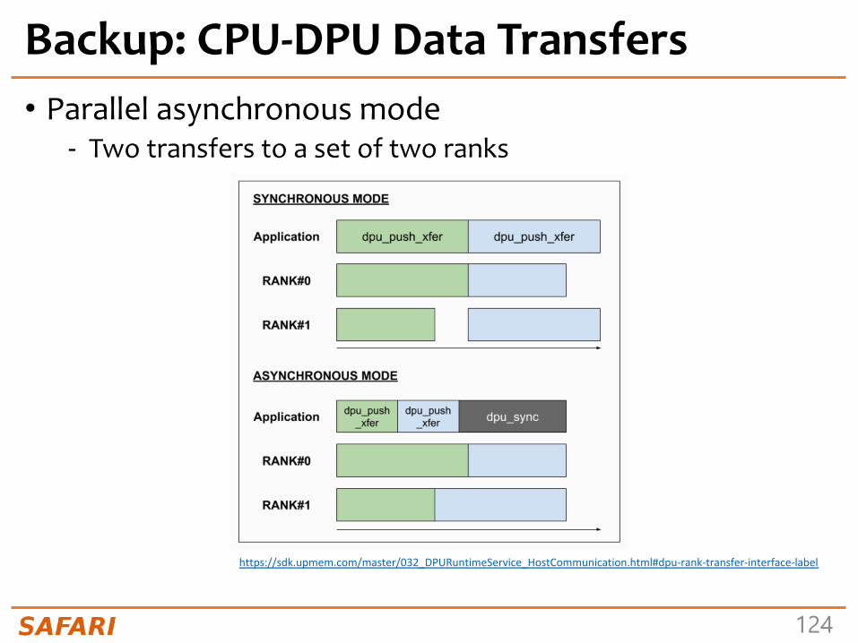
124
Backup: CPU-DPU Data Transfers• Parallel asynchronous mode
- Two transfers to a set of two ranks
https://sdk.upmem.com/master/032_DPURuntimeService_HostCommunication.html#dpu-rank-transfer-interface-label
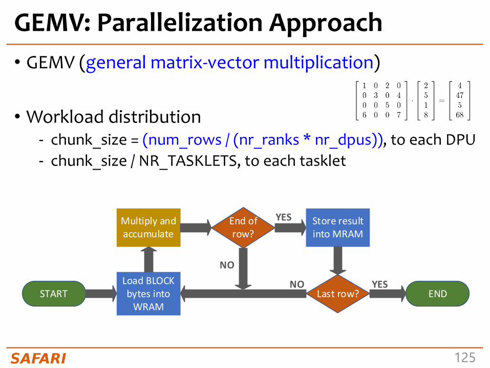
125
GEMV: Parallelization Approach• GEMV (general matrix-vector multiplication)
• Workload distribution- chunk_size = (num_rows / (nr_ranks * nr_dpus)), to each DPU- chunk_size / NR_TASKLETS, to each tasklet
Load BLOCK bytes into
WRAM
Multiply and accumulate
End of row?
Store result into MRAM
Last row? ENDSTART
YES
NO
NO YES
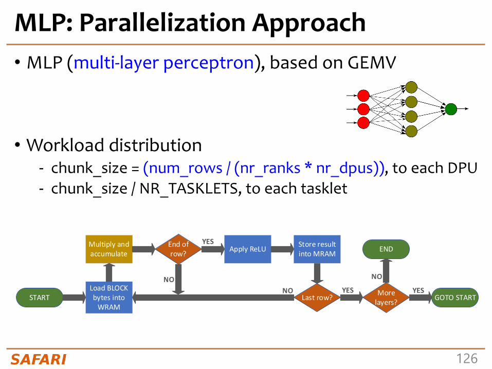
126
MLP: Parallelization Approach• MLP (multi-layer perceptron), based on GEMV
• Workload distribution- chunk_size = (num_rows / (nr_ranks * nr_dpus)), to each DPU- chunk_size / NR_TASKLETS, to each tasklet
Load BLOCK bytes into
WRAM
Multiply and accumulate
End of row? Apply ReLU
Last row?
END
START
YES
NOYES
NO
Store result into MRAM
More layers?
NO YESGOTO START

127
Performance Scaling Results• Strong scaling
• Weak scaling
0
50
100
150
200
250
1 2 4 8 16
Exec
utio
n Ti
me
(ms)
#tasklets per DPUGEMV
RetrieveLoadDPU
0
100
200
300
400
500
600
1 2 4 8 16
Exec
utio
n Ti
me
(ms)
#tasklets per DPUMLP
RetrieveLoadDPU
0
5
10
15
20
25
30
35
1 4 16 64
Exec
utio
n Ti
me
(ms)
#DPUsGEMV
RetrieveLoadHostDPU
0
20
40
60
80
100
120
1 4 16 64
Exec
utio
n Ti
me
(ms)
#DPUsMLP
RetrieveLoadHostDPU

128
PIM Review and Open Problems128
Onur Mutlu, Saugata Ghose, Juan Gomez-Luna, and Rachata Ausavarungnirun,"Processing Data Where It Makes Sense: Enabling In-Memory Computation"Invited paper in Microprocessors and Microsystems (MICPRO), June 2019.[arXiv version]
https://arxiv.org/pdf/1903.03988.pdf

129
PIM Review and Open Problems (II)129
Saugata Ghose, Amirali Boroumand, Jeremie S. Kim, Juan Gomez-Luna, and Onur Mutlu,"Processing-in-Memory: A Workload-Driven Perspective"Invited Article in IBM Journal of Research & Development, Special Issue on Hardware for Artificial Intelligence, to appear in November 2019.[Preliminary arXiv version]
https://arxiv.org/pdf/1907.12947.pdf
Related Documents