BRNO UNIVERSITY OF TECHNOLOGY VYSOKÉ UČENÍ TECHNICKÉ V BRNĚ FACULTY OF ELECTRICAL ENGINEERING AND COMMUNICATION ÚSTAV RADIOELEKTRONIKY FAKULTA ELEKTROTECHNIKY A KOMUNIKAČNÍCH TECHNOLOGIÍ DEPARTMENT OF RADIO ELECTRONICS UNCONVENTIONAL SIGNALS OSCILLATORS OSCILÁTORY GENERUJÍCÍ NEKONVENČNÍ SIGNÁLY DOCTORAL THESIS DOKTORSKÁ PRÁCE AUTHOR Ing. ZDENĚK HRUBOŠ AUTOR PRÁCE SUPERVISOR doc. Ing. JIŘÍ PETRŽELA, Ph.D. VEDOUCÍ PRÁCE BRNO 2016

Welcome message from author
This document is posted to help you gain knowledge. Please leave a comment to let me know what you think about it! Share it to your friends and learn new things together.
Transcript

VYSOKÉ UČENÍ TECHNICKÉ V BRNĚBRNO UNIVERSITY OF TECHNOLOGY
FAKULTA ELEKTROTECHNIKY A KOMUNIKAČNÍCHTECHNOLOGIÍÚSTAV RADIOELEKTRONIKY
FACULTY OF ELECTRICAL ENGINEERING AND COMMUNICATIONDEPARTMENT OF RADIO ELECTRONICS
ANALOGOVÉ OSCILÁTORY GENERUJÍCÍNEKONVENČNÍ SPOJITÉ SIGNÁLY
ANALOG OSCILLATORS GENERATING UNCONVENTIONAL CONTINUOUS-TIME SIGNALS
POJEDNÁNÍDOCTORAL THESIS TOPIC
AUTOR PRÁCE Ing. ZDENĚK HRUBOŠAUTHOR
VEDOUCÍ PRÁCE doc. Ing. JIŘÍ PETRŽELA, Ph.D.SUPERVISOR
BRNO 2016
BRNO UNIVERSITY OF TECHNOLOGYVYSOKÉ UČENÍ TECHNICKÉ V BRNĚVYSOKÉ UČENÍ TECHNICKÉ V BRNĚBRNO UNIVERSITY OF TECHNOLOGY
FAKULTA ELEKTROTECHNIKY A KOMUNIKAČNÍCHTECHNOLOGIÍÚSTAV RADIOELEKTRONIKY
FACULTY OF ELECTRICAL ENGINEERING AND COMMUNICATIONDEPARTMENT OF RADIO ELECTRONICS
ANALOGOVÉ OSCILÁTORY GENERUJÍCÍNEKONVENČNÍ SPOJITÉ SIGNÁLY
ANALOG OSCILLATORS GENERATING UNCONVENTIONAL CONTINUOUS-TIME SIGNALS
POJEDNÁNÍDOCTORAL THESIS TOPIC
AUTOR PRÁCE Ing. ZDENĚK HRUBOŠAUTHOR
VEDOUCÍ PRÁCE doc. Ing. JIŘÍ PETRŽELA, Ph.D.SUPERVISOR
BRNO 2016
FACULTY OF ELECTRICAL ENGINEERING ANDCOMMUNICATIONÚSTAV RADIOELEKTRONIKY
FAKULTA ELEKTROTECHNIKY A KOMUNIKAČNÍCHTECHNOLOGIÍDEPARTMENT OF RADIO ELECTRONICS
UNCONVENTIONAL SIGNALS OSCILLATORSOSCILÁTORY GENERUJÍCÍ NEKONVENČNÍ SIGNÁLY
DOCTORAL THESISDOKTORSKÁ PRÁCE
AUTHOR Ing. ZDENĚK HRUBOŠAUTOR PRÁCE
SUPERVISOR doc. Ing. JIŘÍ PETRŽELA, Ph.D.VEDOUCÍ PRÁCE
BRNO 2016

ABSTRACTThe doctoral thesis deals with electronically adjustable oscillators suitable for signalgeneration, study of the nonlinear properties associated with the active elements usedand, considering these, its capability to convert harmonic signal into chaotic waveform.Individual platforms for evolution of the strange attractors are discussed in detail. In thedoctoral thesis, modeling of the real physical and biological systems exhibiting chaoticbehavior by using analog electronic building blocks and modern functional devices (OTA,MO-OTA, CCII±, DVCC±, etc.) with experimental verification of proposed structuresis presented. One part of theses deals with possibilities in the area of analog–digitalsynthesis of the nonlinear dynamical systems, the study of changes in the mathematicalmodels and corresponding solutions. At the end is presented detailed analysis of theimpact and influences of active elements parasitics in terms of qualitative changes in theglobal dynamic behavior of the individual systems and possibility of chaos destructionvia parasitic properties of the used active devices.
KEYWORDSDynamical system, OTA, MO–OTA, CCII±, electronic adjusting, oscillator, chaos, vectorfield, state attractor, eigenvalues, eigenvectors, Poincaré section, Poincaré map, Lyapu-nov exponents, bifurcation diagram, circuit realizations, autonomous, nonautonomous,practical measurement, digital control, parasitic properties.
ABSTRAKTDizertační práce se zabývá elektronicky nastavitelnými oscilátory, studiem nelineárníchvlastností spojených s použitými aktivními prvky a posouzením možnosti vzniku chaotic-kého signálu v harmonických oscilátorech. Jednotlivé příklady vzniku podivných atraktorůjsou detailně diskutovány. V doktorské práci je dále prezentováno modelování reálnýchfyzikálních a biologických systémů vykazujících chaotické chování pomocí analogovýchelektronických obvodů a moderních aktivních prvků (OTA, MO-OTA, CCII ±, DVCC ±,atd.), včetně experimentálního ověření navržených struktur. Další část práce se zabývámožnostmi v oblasti analogově – digitální syntézy nelineárních dynamických systémů,studiem změny matematických modelů a odpovídajícím řešením. Na závěr je uvedenaanalýza vlivu a dopadu parazitních vlastností aktivních prvků z hlediska kvalitativníchzměn v globálním dynamickém chování jednotlivých systémů s možností zániku chaosuv důsledku parazitních vlastností použitých aktivních prvků.
KLÍČOVÁ SLOVADynamické systémy, OTA, MO–OTA, CCII±, elektronické ladění, oscilátor, chaos, vek-torové pole, stavový atraktor, vlastní čísla, vlastní vektory, Poincarého sekce, Poincaréhomapa, Ljapunovovy exponenty, bifurkační diagram, obvodové realizace, autonomní, ne-autonomní, praktické měření, digitální řízení, parazitní vlastnosti.
HRUBOŠ, Zdeněk Unconventional signals oscillators: doctoral thesis. Brno: Brno Uni-versity of Technology, Faculty of Electrical Engineering and Communication, Ústav ra-dioelektroniky, 2016. 187 p. Supervised by doc. Ing. Jiří Petržela, Ph.D.

DECLARATION
I declare that I have elaborated my doctoral thesis on the theme of “Unconventionalsignals oscillators” independently, under the supervision of the doctoral thesis supervisorand with the use of technical literature and other sources of information which are allquoted in the thesis and detailed in the list of literature at the end of the thesis.
As the author of the doctoral thesis I furthermore declare that, concerning the cre-ation of this doctoral thesis, I have not infringed any copyright. In particular, I havenot unlawfully encroached on anyone’s personal copyright and I am fully aware of theconsequences in the case of breaking Regulation S 11 and the following of the CopyrightAct No 121/2000 Vol., including the possible consequences of criminal law resulted fromRegulation S 152 of Criminal Act No 140/1961 Vol.
Brno . . . . . . . . . . . . . . . . . . . . . . . . . . . . . . . . . . . . . . . . . . . . . . . . .(author’s signature)

ACKNOWLEDGEMENT
I would like to express my gratitude to my supervisor doc. Ing. Jiří Petržela, Ph.D. forgiving me an opportunity to work with him and for his advice and invaluable guidancethroughout my research. Gratitude is also due to my friends Ing. Roman Šotner, Ph.D.and Ing. Tomáš Götthans, Ph.D. for their advice and invaluable guidance throughoutmy research. This thesis would have been impossible without their precious ideas andsupport. Last but not least, I would like to thank my parents, Jaroslava Hrubošová andZdeněk Hruboš, girlfriend MVDr. Alžběta Taláková and family for their patience andgiving me the motivation to finish my studies.
Brno . . . . . . . . . . . . . . . . . . . . . . . . . . . . . . . . . . . . . . . . . . . . . . . . .(author’s signature)
This doctoral thesis is dedicated in memory of my late grandmother, Josefa Hrubošová.

Research described in this doctoral thesis has been implemented in the laboratoriessupported byt the SIX project; reg. no. CZ.1.05/2.1.00/03.0072, operational programResearch and Development for Innovation.
Brno . . . . . . . . . . . . . . . . . . . . . . . . . . . . . . . . . . . . . . . . . . . . . . . . .(author’s signature)
Faculty of Electrical Engineeringand CommunicationBrno University of TechnologyTechnicka 12, CZ-616 00 BrnoCzech Republic
http://www.six.feec.vutbr.cz

CONTENTS
List of symbols, physical constants and abbreviations 19
Preface 23
1 State of the Art 251.1 Active Elements Suitable for Analog Signal Processing . . . . . . . . 25
1.1.1 Methods of Electronic Control in Applications of Modern ActiveElements . . . . . . . . . . . . . . . . . . . . . . . . . . . . . . 25
1.1.2 Comparison of Oscillator with Electronic Control . . . . . . . 261.2 Modeling of the Real Physical and Biological Systems Exhibiting Cha-
otic Behavior . . . . . . . . . . . . . . . . . . . . . . . . . . . . . . . 281.2.1 Visualization Techniques for Quantitative Analysis of Chaos . 29
2 Aims of the Dissertation 32
3 Electronically Adjustable Oscillators Employing Novel Active Ele-ments 333.1 Elements with Controlled Gain . . . . . . . . . . . . . . . . . . . . . 333.2 Oscillator Based on Negative Current Conveyors . . . . . . . . . . . . 38
3.2.1 Proposed Oscillators . . . . . . . . . . . . . . . . . . . . . . . 383.2.2 Simulation and Measurement Results . . . . . . . . . . . . . . 413.2.3 Parasitic Influences . . . . . . . . . . . . . . . . . . . . . . . . 44
3.3 Study of 3R–2C Oscillator . . . . . . . . . . . . . . . . . . . . . . . . 473.3.1 Proposed Oscillators . . . . . . . . . . . . . . . . . . . . . . . 473.3.2 Simulation and Measurement Results . . . . . . . . . . . . . . 51
3.4 Multiphase Oscillator Based on CG–BCVA . . . . . . . . . . . . . . . 583.4.1 Proposed Oscillators . . . . . . . . . . . . . . . . . . . . . . . 583.4.2 Simulation and Measurement Results . . . . . . . . . . . . . . 613.4.3 Quasi–Linear Systems vs. Chaotic Systems . . . . . . . . . . . 66
3.5 Summary . . . . . . . . . . . . . . . . . . . . . . . . . . . . . . . . . 67
4 Modeling of the Real Physical and the Biological Systems 684.1 Autonomous Dynamical Systems . . . . . . . . . . . . . . . . . . . . 684.2 Universal Chaotic Oscillator . . . . . . . . . . . . . . . . . . . . . . . 69
4.2.1 Mathematical Model . . . . . . . . . . . . . . . . . . . . . . . 694.2.2 Mathematical Analysis . . . . . . . . . . . . . . . . . . . . . . 754.2.3 Universal Chaotic Oscillator Circuit Realization . . . . . . . . 76
4.3 Inertia Neuron Model . . . . . . . . . . . . . . . . . . . . . . . . . . . 85

4.3.1 FitzHugh–Nagumo Model . . . . . . . . . . . . . . . . . . . . 854.3.2 Hindmarsh–Rose Model . . . . . . . . . . . . . . . . . . . . . 864.3.3 Circuitry Realization of the Inertia Neuron . . . . . . . . . . . 874.3.4 Simulation and Measurement Results . . . . . . . . . . . . . . 89
4.4 Nóse–Hoover Thermostat Dynamic System . . . . . . . . . . . . . . . 924.4.1 Circuitry Implementation of the Nóse–Hoover System . . . . . 964.4.2 Simulation and Measurement Results . . . . . . . . . . . . . . 97
4.5 Algebraically Simple Three–Dimensional ODE’s . . . . . . . . . . . . 984.5.1 Mathematical Analysis . . . . . . . . . . . . . . . . . . . . . . 984.5.2 Circuitry Realization . . . . . . . . . . . . . . . . . . . . . . . 1014.5.3 Simulation and Measurement Results . . . . . . . . . . . . . . 103
4.6 Chaotic Circuits Based on OTA Elements . . . . . . . . . . . . . . . 1044.6.1 Circuitry Realization . . . . . . . . . . . . . . . . . . . . . . . 107
4.7 Chaotic Circuit Based on Memristor Properties . . . . . . . . . . . . 1104.7.1 Mathematical Analysis . . . . . . . . . . . . . . . . . . . . . . 1114.7.2 Circuitry Realization . . . . . . . . . . . . . . . . . . . . . . . 1154.7.3 Simulation and Measurement Results . . . . . . . . . . . . . . 116
4.8 Nonautonomous Dynamical Systems . . . . . . . . . . . . . . . . . . 1184.8.1 Van der Pol Oscillator (a) . . . . . . . . . . . . . . . . . . . . 1184.8.2 Shaw–Van der Pol Oscillator (b) . . . . . . . . . . . . . . . . . 1184.8.3 Duffing–Van der Pol Oscillator (c) . . . . . . . . . . . . . . . . 1194.8.4 Two–well Duffing Oscillator (d) . . . . . . . . . . . . . . . . . 1194.8.5 Rayleygh–Duffing Oscillator (e) . . . . . . . . . . . . . . . . . 1194.8.6 Ueda Oscillator (f) . . . . . . . . . . . . . . . . . . . . . . . . 1194.8.7 Ueda Oscillator Methematical Anlysis . . . . . . . . . . . . . . 1194.8.8 Circuitry Realization . . . . . . . . . . . . . . . . . . . . . . . 1244.8.9 Simulation and Measurement Results – Voltage Mode . . . . . 1244.8.10 Simulation and Measurement Results – Hybrid Mode . . . . . 127
4.9 Summary . . . . . . . . . . . . . . . . . . . . . . . . . . . . . . . . . 130
5 Analog–Digital Synthesis of theNonlinear Dynamical Systems 131
5.0.1 Mathematical Analysis . . . . . . . . . . . . . . . . . . . . . . 1315.0.2 Circuitry Realization . . . . . . . . . . . . . . . . . . . . . . . 1325.0.3 Simulation and Measurement Results . . . . . . . . . . . . . . 1355.0.4 3D Grid Scrolls . . . . . . . . . . . . . . . . . . . . . . . . . . 139
5.1 Summary . . . . . . . . . . . . . . . . . . . . . . . . . . . . . . . . . 140

6 On the possibility of Chaos Destruction via Parasitic Properties ofthe Used Active Devices 1416.1 Influences of Active Elements Parasitics . . . . . . . . . . . . . . . . . 1426.2 Influence of Parasitic Properties of Active Elements in Circuit Based
on Inertia Neuron Model . . . . . . . . . . . . . . . . . . . . . . . . . 1436.3 Influence of Parasitic Properties of Active Elements in Circuit Based
on Memristor Properties . . . . . . . . . . . . . . . . . . . . . . . . . 1466.3.1 Calculation of Eigenvalues . . . . . . . . . . . . . . . . . . . . 150
6.4 Influence of Parasitic Properties of Active Elements in Circuit Basedon Sprott system . . . . . . . . . . . . . . . . . . . . . . . . . . . . . 1516.4.1 Calculation of Eigenvalues . . . . . . . . . . . . . . . . . . . . 157
6.5 Summary . . . . . . . . . . . . . . . . . . . . . . . . . . . . . . . . . 159
7 Conclusion 160
References 164

LIST OF FIGURES
3.1 Controlled gain negative current conveyor of second generation (CCII-): a) symbol, b) behavioral model. . . . . . . . . . . . . . . . . . . . . 33
3.2 Controlled gain current follower differential output buffered amplifier(CG-CFDOBA): a) symbol, b) behavioral model, c) possible implementation. 34
3.3 Controlled gain current follower buffered amplifier(CG-CFBA): a)symbol, b) behavioral model, c) possible implementation. . . . . . . . 34
3.4 Controlled gain current inverter differential output buffered amplifier(CG-CIBA): a) symbol, b) behavioral model, c) possible implemen-tation. . . . . . . . . . . . . . . . . . . . . . . . . . . . . . . . . . . . 35
3.5 Controlled gain current amplified voltage amplifier (CG-CVA): a)symbol, b) behavioral model, c) possible implementation. . . . . . . . 35
3.6 Controlled gain-buffered current and voltage amplifier CG-BCVA: a)symbol, b) behavioral model, c) behavioral model with additional in-verting buffer output, d) possible implementation using commerciallyavailable ICs (version without additional inverting output). . . . . . . 36
3.7 Adjustable oscillator based on two CCII–: a) basic variant, b) resistor-less variant. . . . . . . . . . . . . . . . . . . . . . . . . . . . . . . . . 38
3.8 Detailed analysis of sensitivity (3.12) of oscillation frequency on pro-duct 𝐵1𝐵2. . . . . . . . . . . . . . . . . . . . . . . . . . . . . . . . . 39
3.9 Time waveforms of the output signals (for 𝑉𝑆𝐸𝑇 _𝐴 = 2 𝑉 , 𝑉𝑆𝐸𝑇 _𝐵 =0 𝑉 ), given by simulation (transient analysis in PSpice). . . . . . . . . 40
3.10 Spectrum of the output signals. . . . . . . . . . . . . . . . . . . . . . 403.11 Measured output signals (larger is 𝑉𝑂𝑈𝑇 1, smaller is 𝑉𝑂𝑈𝑇 2 for 𝑉𝑆𝐸𝑇 _𝐴 =
2𝑉 , 𝑉𝑆𝐸𝑇 _𝐵 = 0𝑉 ).Horizontal axis 500𝑚𝑉/𝑑𝑖𝑣, vertical axis 500𝑚𝑉/𝑑𝑖𝑣. 413.12 Measured spectrum of the output signal. . . . . . . . . . . . . . . . . 423.13 Oscillation frequency versus control voltage. . . . . . . . . . . . . . . 423.14 Output voltages vs. oscillation frequency (measured). . . . . . . . . . 433.15 THD versus oscillation frequency (measured). . . . . . . . . . . . . . 433.16 Important parasitic influences of CCII– . . . . . . . . . . . . . . . . . 443.17 Important parasitic influences in the proposed oscillator. . . . . . . . 443.18 The first proposed oscillator. . . . . . . . . . . . . . . . . . . . . . . . 483.19 The second version of the oscillator. . . . . . . . . . . . . . . . . . . . 493.20 Third version of oscillator with direct electronic adjusting. . . . . . . 503.21 Non-ideal models of used active elements: a) CG-CFBA, b) CG-CIBA. 513.22 Non-ideal models of used active elements: a) CG-CFDOBA, b) CG-
BCVA. . . . . . . . . . . . . . . . . . . . . . . . . . . . . . . . . . . . 523.23 Important parasitic influences in the circuit of the second oscillator. . 52

3.24 Second version of the oscillator with AGC. . . . . . . . . . . . . . . . 533.25 Measured results - transient responses. Horizontal axis 200𝑛𝑠/𝑑𝑖𝑣,
vertical axis 500𝑚𝑉/𝑑𝑖𝑣. . . . . . . . . . . . . . . . . . . . . . . . . . 543.26 Measured results - spectrum of 𝑉𝑂𝑈𝑇 2. . . . . . . . . . . . . . . . . . 543.27 Results of tuning process - dependence of THD on oscillation frequency
𝑓0. . . . . . . . . . . . . . . . . . . . . . . . . . . . . . . . . . . . . . 553.28 Dependence of 𝑓0 on controlled current gain 𝐵1. . . . . . . . . . . . . 553.29 Results of tuning process - dependence of output levels on oscillation
frequency 𝑓0. . . . . . . . . . . . . . . . . . . . . . . . . . . . . . . . 563.30 Dependence of 𝑉𝑂𝑈𝑇 1 on controlled current gain 𝐵1. . . . . . . . . . . 563.31 Basic solution of tunable multiphase oscillator employing two active
elements based on controlled gains. . . . . . . . . . . . . . . . . . . . 583.32 Modification solution of tunable multiphase oscillator employing two
active elements based on controlled gains for differential quadraturesignal generation. . . . . . . . . . . . . . . . . . . . . . . . . . . . . . 59
3.33 Model of proposed oscillator for non–ideal analysis. . . . . . . . . . . 603.34 Transient responses at all available outputs (𝑉𝑂𝑈𝑇 1 - blue color, 𝑉𝑂𝑈𝑇 1𝑖
- green color, 𝑉𝑂𝑈𝑇 2 - red color, 𝑉𝑂𝑈𝑇 3 - orange color) for 𝐵1,2 =1.1 (𝑉𝑓0_𝑐𝑜𝑛𝑡𝑟𝑜𝑙 = 1.15 𝑉 ). Horizontal axis 50 𝑛𝑠/𝑑𝑖𝑣, vertical axis50𝑚𝑉/𝑑𝑖𝑣. . . . . . . . . . . . . . . . . . . . . . . . . . . . . . . . . 61
3.35 Transient responses at 𝑉𝑂𝑈𝑇 1 and 𝑉𝑂𝑈𝑇 2 for𝐵1,2 = 2.9 (𝑉𝑓0_𝑐𝑜𝑛𝑡𝑟𝑜𝑙 = 3.17𝑉 ).Horizontal axis 20 𝑛𝑠/𝑑𝑖𝑣, vertical axis 50𝑚𝑉/𝑑𝑖𝑣. . . . . . . . . . . 62
3.36 Amplitude-automatic gain control circuit for wideband amplitude sta-bilization. . . . . . . . . . . . . . . . . . . . . . . . . . . . . . . . . . 63
3.37 Measured frequency spectrum of 𝑉𝑂𝑈𝑇 1. . . . . . . . . . . . . . . . . . 633.38 Measured frequency spectrum of 𝑉𝑂𝑈𝑇 2. . . . . . . . . . . . . . . . . . 643.39 Dependence of 𝑓0 on adjustable current gains 𝐵1,2. . . . . . . . . . . . 643.40 Additional characteristics - output levels (𝑉𝑂𝑈𝑇 1, 𝑉𝑂𝑈𝑇 2) versus 𝑓0. . . 653.41 Additional characteristics - THD versus 𝑓0. . . . . . . . . . . . . . . . 654.1 PWL function. . . . . . . . . . . . . . . . . . . . . . . . . . . . . . . 704.2 Numerical analysis of three different systems configurations from Tab.
4.1 - projection X-Y. Initial condition 𝑖𝑐 = [0.05, 0, 0]𝑇 , DS-ECEC(top), CH2-ECEC (center), CH3-ECEC (bottom). . . . . . . . . . . . 73
4.3 Bifurcaion diagrams (left) and Poincaré map (right) of three selectedsystems configurations from Tab. 4.1, where 𝑒32 is adopted as a bifur-cation parameter. DS–ECEC (top), CH2–ECEC (center), CH3–ECEC(bottom). . . . . . . . . . . . . . . . . . . . . . . . . . . . . . . . . . 74
4.4 Example of block for setting system parameters 𝑒𝑥. . . . . . . . . . . 764.5 Universal chaotic oscillator schematic. . . . . . . . . . . . . . . . . . . 77

4.6 Plane projections, the first row of the Tab. 4.1. . . . . . . . . . . . . . 784.7 Plane projections, the second row of the Tab. 4.1. . . . . . . . . . . . 784.8 Plane projections, the third row of the Tab. 4.1. . . . . . . . . . . . . 784.9 Plane projections, the fourth row of the Tab. 4.1. . . . . . . . . . . . 794.10 Plane projections, the fifth row of the Tab. 4.1. . . . . . . . . . . . . 794.11 Plane projections, the eight row of the Tab. 4.1. . . . . . . . . . . . . 794.12 Plane projections, the ninth row of the Tab. 4.1. . . . . . . . . . . . . 804.13 Plane projections, the tenth row of the Tab. 4.1. . . . . . . . . . . . . 804.14 Plane projections, the thirteen row of the Tab. 4.1. . . . . . . . . . . 804.15 Plane projections, the sixteenth row of the Tab. 4.1. . . . . . . . . . . 814.16 Experimental results, the first row of the Tab. 4.1. Horizontal axis
2 𝑉/𝑑𝑖𝑣, vertical axis 2 𝑉/𝑑𝑖𝑣 (left), horizontal axis 2 𝑉/𝑑𝑖𝑣, verticalaxis 1 𝑉/𝑑𝑖𝑣 (right). . . . . . . . . . . . . . . . . . . . . . . . . . . . . 81
4.17 Experimental results, the second row of the Tab. 4.1. Horizontal axis2 𝑉/𝑑𝑖𝑣, vertical axis 2 𝑉/𝑑𝑖𝑣 (left), horizontal axis 2 𝑉/𝑑𝑖𝑣, verticalaxis 2 𝑉/𝑑𝑖𝑣 (right). . . . . . . . . . . . . . . . . . . . . . . . . . . . . 81
4.18 Experimental results, the third row of the Tab. 4.1. Horizontal axis2 𝑉/𝑑𝑖𝑣, vertical axis 2 𝑉/𝑑𝑖𝑣 (left), horizontal axis 2 𝑉/𝑑𝑖𝑣, verticalaxis 1 𝑉/𝑑𝑖𝑣 (right). . . . . . . . . . . . . . . . . . . . . . . . . . . . . 82
4.19 Experimental results, the fourth row of the table Tab. 4.1. Horizon-tal axis 2 𝑉/𝑑𝑖𝑣, vertical axis 2 𝑉/𝑑𝑖𝑣 (left), horizontal axis 2 𝑉/𝑑𝑖𝑣,vertical axis 1 𝑉/𝑑𝑖𝑣 (right). . . . . . . . . . . . . . . . . . . . . . . . 82
4.20 Experimental results, the fifth row of the Tab. 4.1. Horizontal axis2 𝑉/𝑑𝑖𝑣, vertical axis 2 𝑉/𝑑𝑖𝑣 (left), horizontal axis 2 𝑉/𝑑𝑖𝑣, verticalaxis 1 𝑉/𝑑𝑖𝑣 (right). . . . . . . . . . . . . . . . . . . . . . . . . . . . . 82
4.21 Experimental results, the eighth row of the Tab. 4.1. Horizontal axis2 𝑉/𝑑𝑖𝑣, vertical axis 2 𝑉/𝑑𝑖𝑣 (left), horizontal axis 2 𝑉/𝑑𝑖𝑣, verticalaxis 1 𝑉/𝑑𝑖𝑣 (right). . . . . . . . . . . . . . . . . . . . . . . . . . . . . 83
4.22 Experimental results, the ninth row of the Tab. 4.1. Horizontal axis2 𝑉/𝑑𝑖𝑣, vertical axis 2 𝑉/𝑑𝑖𝑣 (left), horizontal axis 2 𝑉/𝑑𝑖𝑣, verticalaxis 1 𝑉/𝑑𝑖𝑣 (right). . . . . . . . . . . . . . . . . . . . . . . . . . . . . 83
4.23 Experimental results, the twelfth row of the Tab. 4.1.Horizontal axis2 𝑉/𝑑𝑖𝑣, vertical axis 2 𝑉/𝑑𝑖𝑣 (left), horizontal axis 2 𝑉/𝑑𝑖𝑣, verticalaxis 1 𝑉/𝑑𝑖𝑣 (right). . . . . . . . . . . . . . . . . . . . . . . . . . . . . 83
4.24 Experimental results, the thirteenth row of the Tab. 4.1. Horizon-tal axis 2 𝑉/𝑑𝑖𝑣, vertical axis 2 𝑉/𝑑𝑖𝑣 (left), horizontal axis 2 𝑉/𝑑𝑖𝑣,vertical axis 1 𝑉/𝑑𝑖𝑣 (right). . . . . . . . . . . . . . . . . . . . . . . . 84

4.25 Experimental results, the sixteenth row of the Tab. 4.1. Horizontalaxis 2 𝑉/𝑑𝑖𝑣, vertical axis 2 𝑉/𝑑𝑖𝑣 (left), horizontal axis 2 𝑉/𝑑𝑖𝑣, ver-tical axis 1 𝑉/𝑑𝑖𝑣 (right). . . . . . . . . . . . . . . . . . . . . . . . . . 84
4.26 Experimental results in time domain and power spectrum (AgilentInfiniium). Horizontal axis 5 𝑚𝑠𝑉/𝑑𝑖𝑣, vertical axis 2 𝑉/𝑑𝑖𝑣 (left),horizontal axis 5𝑚𝑠/𝑑𝑖𝑣, vertical axis 2 𝑉/𝑑𝑖𝑣 (right). . . . . . . . . . 84
4.27 Schematicm of the fully analog representation of single inertia neuron. 874.28 Simulated results of the inertia neuron obtained from PSpice - Monge
plane projection. . . . . . . . . . . . . . . . . . . . . . . . . . . . . . 884.29 Simulated results of the qualitatively different behavior of the HR
model. 𝑎 = 2, 6; 𝑏 = 4; 𝑑 = 5; 𝜇 = 0, 01; 𝐼 = 2, 99; (𝑎) 𝑥0 = −0, 6;(𝑏) 𝑥0 = −1, 6; (𝑐) 𝑥0 = −2, 0; (𝑑) 𝑥0 = −2, 4. . . . . . . . . . . . . . 89
4.30 Measured results of the inertia neuron – plane projection and frequencyspectrum (Agilent Infiniium). Horizontal axis 2 𝑉/𝑑𝑖𝑣, vertical axis2 𝑉/𝑑𝑖𝑣. . . . . . . . . . . . . . . . . . . . . . . . . . . . . . . . . . . 90
4.31 Measured results of the qualitatively different behavior of the HRmodel(Agilent Infiniium). 𝑎 = 2, 6; 𝑏 = 4; 𝑑 = 5; 𝜇 = 0, 01; 𝐼 =2, 99; (𝑎) 𝑥0 = −0, 6; (𝑏) 𝑥0 = −1, 6; (𝑐) 𝑥0 = −2, 0; (𝑑) 𝑥0 = −2, 4.Horizontal axis 50𝑚𝑠/𝑑𝑖𝑣, vertical axis 2 𝑉/𝑑𝑖𝑣. . . . . . . . . . . . . 91
4.32 Numerical simulation of the Nóse-Hoover thermostat system – perio-dic (left side), chaotic (right side). . . . . . . . . . . . . . . . . . . . . 92
4.33 Map curve of the sensitivity to change of initial conditions for thesmooth Nóse-Hoover ADDS in the time domain. . . . . . . . . . . . . 93
4.34 Poincare map of sections 𝑦 vs. 𝑧 at plane 𝑥 = 0 of the Nóse-Hooverthermostat system. . . . . . . . . . . . . . . . . . . . . . . . . . . . . 94
4.35 Bifurcation diagram of the Nóse-Hoover thermostat system, wherebifurcation parameter is sensitivity to change of initial conditions. . . 95
4.36 Circuit realization of the Nóse-Hoover thermostat system with AD844as a non–inverting integrator. . . . . . . . . . . . . . . . . . . . . . . 95
4.37 Simulation results of the Nóse-Hoover oscillator – periodic (left side),chaotic(right side). . . . . . . . . . . . . . . . . . . . . . . . . . . . . . . . . 96
4.38 Measurements results of the Nóse-Hoover oscillator – periodic (leftside), chaotic (right side). Horizontal axis 500 𝑚𝑉/𝑑𝑖𝑣, vertical axis2 𝑉/𝑑𝑖𝑣(top left), horizontal axis 1 𝑉/𝑑𝑖𝑣, vertical axis 5 𝑉/𝑑𝑖𝑣(topright), horizontal axis 1 𝑉/𝑑𝑖𝑣, vertical axis 2 𝑉/𝑑𝑖𝑣(bottom left),horizontal axis 5 𝑉/𝑑𝑖𝑣, vertical axis 5 𝑉/𝑑𝑖𝑣(bottom right) . . . . . . 97
4.39 Convergence plot of the largest Lyapunov exponents for 𝑎 = 0.42. . . 984.40 Bifurcation diagram of the Sprott system (4.29). . . . . . . . . . . . . 99

4.41 Numerical simulation of system (4.29) for 𝑎 = 0.37 – limit cycle (leftside) and for 𝑎 = 0.42 – chaos (right side). . . . . . . . . . . . . . . . 99
4.42 Sensitivity to initial conditions in the time domain. . . . . . . . . . . 1004.43 Numerical simulation of system (4.29) for 𝑎 = 0.42. . . . . . . . . . . 1004.44 Schematic of the Sprott system circuitry realization. . . . . . . . . . . 1014.45 Numerical simulation of the Sprott system (4.29) for 𝑎 = 0.42 – chaos. 1024.46 Measured data of realized circuit for 𝑅6 = 400Ω. Horizontal axis 𝑉1
500𝑚𝑉/𝑑𝑖𝑣, vertical axis 𝑉2 1𝑉/𝑑𝑖𝑣. . . . . . . . . . . . . . . . . . . . 1024.47 Bifurcation diagram of system (4.37), bifurcation parameter is sensi-
tivity to change of parameter 𝑎. . . . . . . . . . . . . . . . . . . . . . 1054.48 Bifurcation diagram of system (4.38), bifurcation parameter is sensi-
tivity to change of parameter 𝑏. . . . . . . . . . . . . . . . . . . . . . 1054.49 Circuitry implementation of Eq.(4.37) using OPA860. The capacitors
are 470 𝑛𝐹 , the resistor is 1 𝑘Ω and except for the variable resistor(adjustable from 0 to 1 𝑘Ω). . . . . . . . . . . . . . . . . . . . . . . . 106
4.50 Circuitry implementation of Eq.(4.38) using OPA860. The capacitorsare 470𝑛𝐹 , DC current source is 1𝑚𝐴, the resistor is 1𝑘Ω and exceptfor the variable resistor (adjustable from 0 to 1 𝑘Ω). . . . . . . . . . . 107
4.51 Simulation results for the circuit realized according to the Eq. 4.37 (seeFig. 4.47) - 𝑅 = 950 Ω. Plane projection X-Z corresponds with plane𝑎 in bifurcation diagram (see Fig. 4.47) - period 2. . . . . . . . . . . . 108
4.52 Simulation results for the circuit realized according to the Eq. 4.37 (seeFig. 4.47) - 𝑅 = 800 Ω. Plane projection X-Z corresponds with plane𝑏 in bifurcation diagram (see Fig. 4.47) - period 4. . . . . . . . . . . . 108
4.53 Simulation results for the circuit realized according to the Eq. 4.37 (seeFig. 4.47) - 𝑅 = 785 Ω. Plane projection X-Z corresponds with plane𝑐 in bifurcation diagram (see Fig. 4.47) - period 8. . . . . . . . . . . . 108
4.54 Simulation results for the circuit realized according to the Eq. 4.37 (seeFig. 4.47) - 𝑅 = 735 Ω. Plane projection X-Z corresponds with plane𝑑 in bifurcation diagram (see Fig. 4.47) - chaos. . . . . . . . . . . . . 108
4.55 Simulation results for the circuit realized according to the Eq. 4.38 (seeFig. 4.48) - 𝑅 = 245 Ω. Plane projection X-Z corresponds with plane𝑎 in bifurcation diagram (see Fig. 4.48) - period 2. . . . . . . . . . . . 109
4.56 Simulation results for the circuit realized according to the Eq. 4.38 (seeFig. 4.48) - 𝑅 = 260 Ω. Plane projection X-Z corresponds with plane𝑏 in bifurcation diagram (see Fig. 4.48) - period 4. . . . . . . . . . . . 109
4.57 Simulation results for the circuit realized according to the Eq. 4.38 (seeFig. 4.48) - 𝑅 = 275 Ω. Plane projection X-Z corresponds with plane𝑐 in bifurcation diagram (see Fig. 4.48) - period 8. . . . . . . . . . . . 109

4.58 Simulation results for the circuit realized according to the Eq. 4.38 (seeFig. 4.48) - 𝑅 = 271 Ω. Plane projection X-Z corresponds with plane𝑑 in bifurcation diagram (see Fig. 4.48) - chaos. . . . . . . . . . . . . 109
4.59 Numerical simulation in MathCAD and Poincare section (blue dots)which is formed by 𝑥− 𝑧 plane sliced at 𝑦 = 0 (green surface). . . . . 110
4.60 Plot of 𝑥(𝑡) versus 𝑦(𝑡) (left) and 𝑥(𝑡) versus 𝑧(𝑡) (right) plane pro-jection of the chaotic attractor generated by Eq. (4.43) - numericalsolution. . . . . . . . . . . . . . . . . . . . . . . . . . . . . . . . . . . 111
4.61 Time domain curve of the system system sensitivity to the changesin initial conditions. Initial conditions: 𝑥0 = 0.1, 𝑦0 = 0, 𝑧0 = 0.1and 𝛼 = 0.6 (continuous trace), 𝑥𝑛0 = 0.11, 𝑦𝑛0 = 0, 𝑧𝑛0 = 0.11and 𝛼 = 0.6 (dashed trace). . . . . . . . . . . . . . . . . . . . . . . 112
4.62 Convergence plot of the largest Lyapunov exponents determined byEq. (4.43); 𝛼 = 0.6. . . . . . . . . . . . . . . . . . . . . . . . . . . . . 113
4.63 Bifurcation diagram generated by Eg. (4.43). The bifurcation para-meter 𝛼 is shown on the horizontal axis of the plot. . . . . . . . . . . 114
4.64 Circuit realization of the chaotic system with OTA (OPA860), MO-OTA (MAX435) and analog multiplier (AD633) based on Eq. (4.43).Capacitors are 470nF and resistors are 𝑅1 = 15 Ω, 𝑅2 = 100 Ω. Resis-tor 𝑅3 should be adjustable from 0 to 1 𝑘Ω. . . . . . . . . . . . . . . 115
4.65 Simulation in PSpice with indication of the 𝑥−𝑧 plane sliced at 𝑦 = 0(green surface) . . . . . . . . . . . . . . . . . . . . . . . . . . . . . . 116
4.66 Plot of 𝑣𝑥(𝑡) versus 𝑣𝑦(𝑡) (left) and 𝑣𝑥(𝑡) versus 𝑣𝑦(𝑡) (right) planeprojection of the chaotic attractor – PSpice simulation. . . . . . . . . 117
4.67 Measured data of realized circuit (Fig. 4.64). Horizontal axis 500𝑚𝑉/𝑑𝑖𝑣,vertical axis 500 𝑚𝑉/𝑑𝑖𝑣 (left), horizontal axis 500𝑚𝑉/𝑑𝑖𝑣, verticalaxis 1 𝑉/𝑑𝑖𝑣 (right). . . . . . . . . . . . . . . . . . . . . . . . . . . . . 117
4.68 Numerical simulations of the nonautonomous dynamical systems witha sinusoidally varying driving force. . . . . . . . . . . . . . . . . . . . 120
4.69 Divergence of nearby trajectories caused by small changes in initialconditions in time domain. . . . . . . . . . . . . . . . . . . . . . . . . 121
4.70 Poincare maps of Ueda Attractor. . . . . . . . . . . . . . . . . . . . . 1224.71 Bifurcation diagrams – dependence on the angular velocity of the
driven signal (left side) and dependence on the amplitude of the drivensignal (right side). . . . . . . . . . . . . . . . . . . . . . . . . . . . . . 122
4.72 The Ueda oscillator plane projection dependent on the change of thedriven frequency - numerical integration. . . . . . . . . . . . . . . . . 123
4.73 Circuitry implementation of the mathematical model in voltage mode. 124

4.74 The plane projections of the chaos oscillator obtained from PSpicesimulation – voltage mode. . . . . . . . . . . . . . . . . . . . . . . . . 125
4.75 Measured results of the chaos oscillator in voltage mode – plane pro-jections and frequency spectrum (Agilent Infiniium). Horizontal axis1 𝑉/𝑑𝑖𝑣, vertical axis 1 𝑉/𝑑𝑖𝑣 . . . . . . . . . . . . . . . . . . . . . . 126
4.76 Circuitry implementation of the mathematical model in hybrid mode. 1274.77 The plane projections of the chaos oscillator obtained from PSpice
simulation – hybrid mode. . . . . . . . . . . . . . . . . . . . . . . . . 1284.78 Measured results of the chaos oscillator in hybrid mode – plane pro-
jections and frequency spectrum (Agilent Infiniium). Horizontal axis1 𝑉/𝑑𝑖𝑣, vertical axis 2 𝑉/𝑑𝑖𝑣 . . . . . . . . . . . . . . . . . . . . . . 129
5.1 The model of step function 𝑓(𝑥) for 2𝑏 (black) and for 5𝑏 (gray). . . 1325.2 Numerical simulation of system (5.1), the Monge’s projections 𝑉 (𝑥)
vs. 𝑉 (𝑦). . . . . . . . . . . . . . . . . . . . . . . . . . . . . . . . . . 1335.3 Numerical simulation of system (5.1), the Monge’s projections 𝑉 (𝑦)
vs. 𝑉 (𝑧). . . . . . . . . . . . . . . . . . . . . . . . . . . . . . . . . . 1335.4 The block schematics of realization of equations (5.1). . . . . . . . . 1345.5 The block schematics of realization of function 𝑓(𝑥) using data con-
verters. . . . . . . . . . . . . . . . . . . . . . . . . . . . . . . . . . . 1345.6 The simulations from PSpice program, V(x)versus V(y) projections. . 1355.7 The simulations from PSpice program, V(x)versus V(y) projections. . 1365.8 The simulations from PSpice program, V(x)versus V(y) projections. . 1365.9 1–D 4 scroll. Projections V(x) vs V(-y) (left), V(-y) vs V(z) (right).
Horizontal axis 1 𝑉/𝑑𝑖𝑣, vertical axis 500 𝑚𝑉/𝑑𝑖𝑣 (left), horizontalaxis 1 𝑉/𝑑𝑖𝑣, vertical axis 2 𝑉/𝑑𝑖𝑣 (right). . . . . . . . . . . . . . . . 137
5.10 1–D 16 scroll. Projections V(x) vs V(-y) (left), V(-y) vs V(z) (right).Horizontal axis 1 𝑉/𝑑𝑖𝑣, vertical axis 500 𝑚𝑉/𝑑𝑖𝑣 (left), horizontalaxis 1 𝑉/𝑑𝑖𝑣, vertical axis 500𝑚𝑉/𝑑𝑖𝑣 (right). . . . . . . . . . . . . . 137
5.11 Measured system, 2x2 scroll. Projections V(x) vs V(-y) (left), V(-y)vs V(z) (right). Horizontal axis 1 𝑉/𝑑𝑖𝑣, vertical axis 2 𝑉/𝑑𝑖𝑣 (left),horizontal axis 1 𝑉/𝑑𝑖𝑣, vertical axis 2 𝑉/𝑑𝑖𝑣 (right). . . . . . . . . . . 137
5.12 Measured system, 4x4 scroll. Projections V(x) vs V(-y) (left), V(-y)vs V(z) (right). Horizontal axis 1 𝑉/𝑑𝑖𝑣, vertical axis 2 𝑉/𝑑𝑖𝑣 (left),horizontal axis 1 𝑉/𝑑𝑖𝑣, vertical axis 2 𝑉/𝑑𝑖𝑣 (right). . . . . . . . . . . 138
5.13 Measured system - perturbation of parrameters, 6x4 scroll (left) and4x2 scroll (right). Projections 𝑉 (𝑥) vs. 𝑉 (−𝑦). Horizontal axis 1𝑉/𝑑𝑖𝑣,vertical axis 2𝑉/𝑑𝑖𝑣 (left), horizontal axis 1𝑉/𝑑𝑖𝑣, vertical axis 2𝑉/𝑑𝑖𝑣(right). . . . . . . . . . . . . . . . . . . . . . . . . . . . . . . . . . . . 138

5.14 Measured system, 6x6 scroll. Projections 𝑉 (𝑥) vs. 𝑉 (−𝑦) (left), 8x8scroll, projections 𝑉 (𝑥) vs. 𝑉 (−𝑦) (right). Horizontal axis 1 𝑉/𝑑𝑖𝑣,vertical axis 2𝑉/𝑑𝑖𝑣 (left), horizontal axis 1𝑉/𝑑𝑖𝑣, vertical axis 2𝑉/𝑑𝑖𝑣(right). . . . . . . . . . . . . . . . . . . . . . . . . . . . . . . . . . . . 138
5.15 Numerically simulated 3D (10,10,10) grid scolls. . . . . . . . . . . . . 1396.1 Non-ideal model of operational transconductance amplifier (OTA). . . 1426.2 Non-ideal model of multiple output operational transconductance am-
plifier (MO-OTA). . . . . . . . . . . . . . . . . . . . . . . . . . . . . 1436.3 Influence of parasitic capacitances on the size of the 𝐿𝐸𝑚𝑎𝑥 as a
function of 𝐶𝑝1 and 𝐶𝑝2. . . . . . . . . . . . . . . . . . . . . . . . . . 1446.4 Influence of parasitic capacitances on the size of the 𝐿𝐸𝑚𝑎𝑥 as a
function of 𝐶𝑝1 and 𝐶𝑝3. . . . . . . . . . . . . . . . . . . . . . . . . . 1446.5 Influence of parasitic capacitances on the size of the 𝐿𝐸𝑚𝑎𝑥 as a
function of 𝐶𝑝2 and 𝐶𝑝3. . . . . . . . . . . . . . . . . . . . . . . . . . 1446.6 Influence of parasitic conductances on the size of the 𝐿𝐸𝑚𝑎𝑥 as a
function of 𝐺𝑝1 and 𝐺𝑝2. . . . . . . . . . . . . . . . . . . . . . . . . . 1446.7 Influence of parasitic conductances on the size of the 𝐿𝐸𝑚𝑎𝑥 as a
function of 𝐺𝑝1 and 𝐺𝑝3. . . . . . . . . . . . . . . . . . . . . . . . . . 1446.8 Influence of parasitic conductances on the size of the 𝐿𝐸𝑚𝑎𝑥 as a
function of 𝐺𝑝2 and 𝐺𝑝3. . . . . . . . . . . . . . . . . . . . . . . . . . 1446.9 Circuit realization of the chaotic system with influence of parasitic
properties of active elements. . . . . . . . . . . . . . . . . . . . . . . 1466.10 Numerical analysis of system with memristor properties and influ-
ence of parasitic elements - projection X-Y (red-with parasitic, blue-without parasitic). . . . . . . . . . . . . . . . . . . . . . . . . . . . . 148
6.11 Influence of parasitic conductances on the size of the 𝐿𝐸𝑚𝑎𝑥 as afunction of OPA860 parasitic conductance. . . . . . . . . . . . . . . . 148
6.12 Influence of parasitic conductances on the size of the 𝐿𝐸𝑚𝑎𝑥 as afunction of MAX435 parasitic conductance. . . . . . . . . . . . . . . . 148
6.13 Influence of parasitic conductances on the size of the 𝐿𝐸𝑚𝑎𝑥 as afunction of OPA860 and MAX435 input parasitic conductances. . . . 149
6.14 Influence of parasitic conductances on the size of the 𝐿𝐸𝑚𝑎𝑥 as afunction of OPA860 and MAX435 output parasitic conductances. . . 149
6.15 Influence of parasitic capacitances on the size of the 𝐿𝐸𝑚𝑎𝑥 as afunction of OPA860 parasitic capacitance. . . . . . . . . . . . . . . . 149
6.16 Influence of parasitic capacitances on the size of the 𝐿𝐸𝑚𝑎𝑥 as afunction of MAX435 parasitic capacitance. . . . . . . . . . . . . . . . 149
6.17 Influence of parasitic capacitances on the size of the 𝐿𝐸𝑚𝑎𝑥 as afunction of OPA860 and MAX435 input parasitic capacitances. . . . . 149

6.18 Influence of parasitic capacitances on the size of the 𝐿𝐸𝑚𝑎𝑥 as afunction of OPA860 and MAX435 output parasitic capacitances. . . . 149
6.19 Schematic of circuit realization with important parasitic influences. . 1516.20 Numerical analysis with influence of parasitic elements - projection
X-Y (red - with parasitic, blue - without parasitic). . . . . . . . . . . 1536.21 Circuit simulation with influence of parasitic elements (left - with
parasitic, right - with parasitic compensate ). . . . . . . . . . . . . . . 1546.22 Influence of parasitic capacitances on the size of the 𝐿𝐸𝑚𝑎𝑥 as a
function of 𝐶𝑝1 and 𝐶𝑝2. . . . . . . . . . . . . . . . . . . . . . . . . . 1546.23 Influence of parasitic capacitances on the size of the 𝐿𝐸𝑚𝑎𝑥 as a
function of 𝐶𝑝1 and 𝐶𝑝𝑝3. . . . . . . . . . . . . . . . . . . . . . . . . 1546.24 Influence of parasitic capacitances on the size of the 𝐿𝐸𝑚𝑎𝑥 as a
function of 𝐶𝑝1 and 𝐶𝑝𝑝4. . . . . . . . . . . . . . . . . . . . . . . . . 1546.25 Influence of parasitic capacitances on the size of the 𝐿𝐸𝑚𝑎𝑥 as a
function of 𝐶𝑝2 and 𝐶𝑝𝑝3. . . . . . . . . . . . . . . . . . . . . . . . . 1546.26 Influence of parasitic capacitances on the size of the 𝐿𝐸𝑚𝑎𝑥 as a
function of 𝐶𝑝2 and 𝐶𝑝𝑝4. . . . . . . . . . . . . . . . . . . . . . . . . 1556.27 Influence of parasitic capacitances on the size of the 𝐿𝐸𝑚𝑎𝑥 as a
function of 𝐶𝑝𝑝3 and 𝐶𝑝𝑝4. . . . . . . . . . . . . . . . . . . . . . . . 1556.28 Influence of parasitic conductances on the size of the 𝐿𝐸𝑚𝑎𝑥 as a
function of 𝐺𝑝1 and 𝐺𝑝2. . . . . . . . . . . . . . . . . . . . . . . . . . 1556.29 Influence of parasitic conductances on the size of the 𝐿𝐸𝑚𝑎𝑥 as a
function of 𝐺𝑝1 and 𝐺𝑝3. . . . . . . . . . . . . . . . . . . . . . . . . . 1556.30 Influence of parasitic conductances on the size of the 𝐿𝐸𝑚𝑎𝑥 as a
function of 𝐺𝑝1 and 𝐺𝑝4. . . . . . . . . . . . . . . . . . . . . . . . . . 1556.31 Influence of parasitic conductances on the size of the 𝐿𝐸𝑚𝑎𝑥 as a
function of 𝐺𝑝2 and 𝐺𝑝3. . . . . . . . . . . . . . . . . . . . . . . . . . 1556.32 Influence of parasitic conductances on the size of the 𝐿𝐸𝑚𝑎𝑥 as a
function of 𝐺𝑝2 and 𝐺𝑝4. . . . . . . . . . . . . . . . . . . . . . . . . . 1566.33 Influence of parasitic conductances on the size of the 𝐿𝐸𝑚𝑎𝑥 as a
function of 𝐺𝑝3 and 𝐺𝑝4. . . . . . . . . . . . . . . . . . . . . . . . . . 1566.34 Influence of parasitic conductance and capacitance on the size of the
𝐿𝐸𝑚𝑎𝑥 as a function of 𝐺𝑝1 and 𝐶𝑝1. . . . . . . . . . . . . . . . . . . 1566.35 Influence of parasitic conductance and capacitance on the size of the
𝐿𝐸𝑚𝑎𝑥 as a function of 𝐺𝑝2 and 𝐶𝑝2. . . . . . . . . . . . . . . . . . . 1566.36 Influence of parasitic conductance and capacitance on the size of the
𝐿𝐸𝑚𝑎𝑥 as a function of 𝐺𝑝3 and 𝐶𝑝𝑝3. . . . . . . . . . . . . . . . . . 1566.37 Influence of parasitic conductance and capacitance on the size of the
𝐿𝐸𝑚𝑎𝑥 as a function of 𝐺𝑝4 and 𝐶𝑝𝑝4. . . . . . . . . . . . . . . . . . 156

LIST OF TABLES
4.1 Parameteres of different dynamical systems. . . . . . . . . . . . . . . 754.2 Position of critical points according to the system with PWL function.1044.3 Numerically calculated eigenvalues of both systems. . . . . . . . . . . 106

LIST OF SYMBOLS, PHYSICAL CONSTANTSAND ABBREVIATIONS
𝐴 adjustable voltage gain
A square matrix, dimension is in most cases 3 × 3
A𝑇 transpose of a matrix A
𝐴𝑔 voltage gain
b,w columns vectors, dimension is in most cases 3 × 1
𝐵 current gain
𝐵𝑊 badnwidth
𝐶𝑂 condition of oscillation
𝐶𝑝 parasitic capacitance
𝐶𝑖𝑛_𝑂𝑇 𝐴 OTA input capacitance
𝐶𝑖𝑛_𝑀𝑂𝑂𝑇 𝐴 MO-OTA input capacitance
𝐶𝑜𝑢𝑡_𝑂𝑇 𝐴 OTA output capacitance
𝐶𝑖𝑛_𝑀𝑂𝑂𝑇 𝐴 MO-OTA input capacitance
𝑓0 oscillation frequency
𝑓𝑇 transient frequency
𝑔𝑚 transcoductance (controllable by bias current)
𝐺𝑝 parasitic admittance
I unit matrix, dimension is in most cases 3 × 3
J Jacobian matrix
𝑈𝑋 , 𝑈𝑌 , 𝑈𝑍 input voltage of CC (CCII) or analog multiplier
𝐼𝑆𝐸𝑇 bias control current
𝐼𝑋 , 𝐼𝑌 , 𝐼𝑍 input current of CC (CCII) or current multiplier
PWL piecewise-linear function
19

Q quality factor
R𝑛 n-dimensional state space
𝑅𝑖𝑛_𝑂𝑇 𝐴 OTA input resistance
𝑅𝑖𝑛_𝑀𝑂𝑂𝑇 𝐴 MO-OTA input resistance
𝑅𝑝 parasitic resistance
𝑅𝑖𝑛_𝑂𝑇 𝐴 OTA output resistance
𝑅𝑖𝑛_𝑀𝑂𝑂𝑇 𝐴 MO-OTA output resistance
𝑅𝑥 intrinsic resistance (controllable by bias current)
𝑈𝑆𝐸𝑇 bias control voltage
𝑈𝑋 , 𝑈𝑌 , 𝑈𝑍 input voltage of CC (CCII) or analog multiplier
w𝑇 transpose of a vector w
x derivative of a function x
x0 vector of initial conditions
· scalar product of vectors
→ right side results from left side
ADS autonomous dynamical system
NDS nonautonomous dynamical system
ADDS autonomous deterministic dynamical system
NDDS nonautonomous deterministic dynamical system
CH this chaotic attractor is typical for class C or L of dynamical systems,corresponding with his shape attractor is socalled “single-scroll”
DS this chaotic attractor is typical for class C of dynamical systems,corresponding with his shape attractor is socalled “double–scroll”
CDCD this chaotic attractor is typical for class C or L of dynamical systems,whose state matrix are in block triangular form and contain a complexdecomposed second-order submatrix
20

ECEC chaotic attractor is typical for class C or L of dynamical systems, whosestate matrix are in block triangular form and contain an elementarycanonically decomposed of second order submatrix
VB voltage buffer
VF voltage follower
CA current amplifier
CC current conveyor
OTA operational transconductance amplifier
MO-OTA multi-output operational transconductance amplifier
DO-OTA dual output OTA
CCI first generation current conveyor
CCII second generation current conveyor
CCCII translinear current conveyor/ current controlled CCII
CCTA current conveyor transconductance amplifier
CCCTA current controlled current conveyor transconductance amplifier
CCCDTA current controlled CDTA
DCCF digitally controlled current follower
CDBA current differencing buffered amplifier
CDTA current differencing transconductance amplifier
MCDTA modified CDTA
CFA current feedback amplifier
CC-CFA current controlled current feedback amplifier
DBTA differential-input buffered and transconductance amplifier
DO-CCII/CCCII dual output CCII/ dual output CCCII
MO-CCII/CCCII multiple output CCII/ multiple output CCCII
21

ECCII/CCII electronically controllable current conveyor of second generation/current conveyor of second generation
DVCC differential voltage current conveyor
GCFTA generalized current follower transconductance amplifie
MCDTA modified CDTA
OPAMP operational amplifier
VDIBA voltage differencing inverting buffered amplifier
CG-BCVA controlled gain buffered current and voltage amplifier
CG-CFDOBA controlled gain current follower differential output bufferedamplifier
CG-CIBA controlled gain current inverter buffered amplifier
CG-ICVA controlled gain inverted current and voltage amplifier
DCC-CFA double current controlled - current feedback amplifier
DCCF digitally controlled current follower
ZC-CG-CDBA Z-copy controlled gain current differencing buffered amplifier
PCA programmable current amplifier
22

PREFACE
„In truth at first Chaos came to be, but next wide-bosomed Earth. . . “Hesiod’s Theogony
Chaotic motion is a very specific solution of a nonlinear dynamics systemswhich commonly exists in nature. Its wide area of applications ranges from sim-ple predator–prey models to complicated signal transduction pathways in biologicalcells, from the motion of a pendulum to complex climate models in physics, andbeyond that to further fields as diverse as chemistry (reaction kinetics), economics,engineering, sociology or demography. In particular, this broad scope of applicati-ons has provided a significant impact on the theory of dynamical systems itself, andis one of the main reasons for its popularity over the last decades [126]. It cameas a surprise to most scientists when Lorenz in 1963 discovered chaos in a simplesystem of three autonomous ordinary differential equations with a two quadraticnonlinearities [87].
The solutions of the considered dynamical systems are a state trajectories whichare usually displayed in the state area or extended in time. Each autonomous deter-ministic dynamical system (ADDS) and non–autonomous deterministic dynamicalsystem (NDDS) are fully described by a set of differential equations and initial con-ditions. Behavior of the ADDS and NDDS should be completely predictable in everytime (point of view is that system should go determine by using the phase flow inevery time). Nevertheless, it is true for a linear ADDS and NDDS. In this case thesolution can be only a limit point or a limit cycle enclosed in a final volume. Suggestthat for some a special nonlinear systems, this long-term prediction of the positioncan not be done. The problem is in extreme sensitivity to initial conditions in whichcase is completely different pattern for the small variation in the state trajectory.For classical autonomous dynamical systems the basic law of evolution is staticin the sense that the environment does not change with time. However, in manyapplications such a static approach is too restrictive and a temporally fluctuatingenvironment favorable. For example, the parameters in real–world situations arerarely constant over time. This has various reasons, like absence of lab conditions,adaption processes, seasonal effects, changes in nutrient supply, or an intrinsic bac-kground noise. It must be noted that in practice there is always a particular degreeof imprecision in setting of the initial conditions. It all leads to study infuence ofparasitic properties.
Two basic requirements must be meet for beginning of the chaotic oscillations.The first of them was believed to be an unstable hyperbolic fixed point which gua-rantee that two trajectories going in the neighbourhood are repelled from each other.
23

Divergence of two trajectories be call in this case as a "stretching". This process gu-arantee sensitivity to initial conditions of the system. In this way is also necessaryto eliminate expansion of the system by using curvature of the vector space bynon-linear functions. It is call as a "folding". Whereas that two distinct state spacetrajectories cannot intersect, chaotic ADDS must have at least three state variables.We can say that chaotic attractor is not periodic nor stochastic, however is boundedand looks as a particular element of randomness. Nonlinearity can be represented asmultiply of two state variables, the power of one or as a piecewise linear function,etc. This is important also in the case of various electronic circuits. Chaos has beenobserved in the oscillators with frequency dependent feedback, oscillators with ne-gative resistance elements, etc. The problems covered by chaos theory are universaland can be also observed in the nonautonomous nonlinear dynamical systems withat least two degrees of freedom. There exist many examples where chaos is unwan-ted phenomenon and can be observed in the networks which are basically linear, forexample in filters, oscillators, etc.
24

1 STATE OF THE ART
In this chapter we present the state of the art in the field of active elements suitablefor analog signal processing and modeling of the real physical, biological systemsexhibiting chaotic behavior by using analog electronic circuits and techniques forvisualization and quantification of chaos.
1.1 Active Elements Suitable for Analog SignalProcessing
Many active elements that are suitable for analog signal processing were introducedin [15]. Some of them have interesting features, which allow electronic control of theirparameters. Therefore, these elements have also favorable features in applications.There are several common ways of electronic control of parameters in particularapplications. Development in this field was started with discovery and developmentof current conveyors (CC) by Smith and Sedra [144, 145], Fabre [30] and Svobodaet al. [167]. Many other active elements with possibilities of electronic adjustabilitywere introduced, innovated and frequently utilized for circuit synthesis and designin the past, for example operational transconductance amplifier (OTA) [38], currentfeedback amplifiers (CFA) [15, 107, 136], etc. Great review of old and also recentdiscoveries in the field of active elements was summarized by Biolek et al. [15].Extensive description of many modifications and novel approaches is given in [15]and in references cited therein.
1.1.1 Methods of Electronic Control in Applications of Mo-dern Active Elements
Basic way how to control parameters in applications is by manual change of valuesof passive elements - floating or grounded resistors in most cases (see [39, 44, 47,91, 95, 149], for example). Electronic control requires additional element (e.g. FETtransistor [39]) and the final solution is more complicated generally. Better way is touse so-called bias currents for direct electronic control of parameters of active ele-ments (OTA-s, CC-s, ...). Adjusting of the intrinsic resistance (RX) by bias current(Ibias) is very common solution of control of parameters of many application employ-ing current conveyors [11, 27, 32, 53, 131] or adjustable current feedback amplifiers[142, 152, 150]. Similarly, adjusting of the transconductance value of the OTA [38]also requires bias current control [12, 20, 36, 77, 79, 84, 130, 141, 147, 153, 170].
25

The next method which is used is the current gain adjusting. Development of thismethod has been started together with development of so-called current followers(CF) [15] and its derivatives [1, 16, 40, 41, 53, 94, 148]. Applications of adjustablecurrent followers and amplifiers (in order to control current gain) were reported in[127, 135, 169], for example. Many authors implemented current gain controllingmechanism also to current conveyors and amplifiers [31, 46, 75, 76, 93, 99, 139, 156,166, 168]. Several conceptions also utilize combination of two methods of adjusting(two parameters) [76, 93, 99]. Minaei et al. [99], Kumngern et al. [76] and Sotner etal. [152, 150] presented several different design methods of current conveyors withpossibility of intrinsic resistance and current gain control, Marcellis et al. [93] hasdesigned conveyor with simultaneous adjusting of current and voltage gain. Digitalcontrol of current gain achieved increasing attention in recent years. El-Adawy et al.[26] and Alzaher et al. [5, 6, 7] introduced digitally programmable current followers,amplifiers and current conveyors, respectively.
1.1.2 Comparison of Oscillator with Electronic Control
A short comparison of several oscillator realizations with electronic control is givenat this place.
Sotner et al. [150] engaged three so-called double current-controlled current fe-edback amplifiers (DCC-CFA) in quadrature oscillator solution. Circuit has advan-tages of non-interactive electronic controllability of condition of oscillation (CO) andoscillation frequency (𝑓0) without impact on changes of output amplitudes duringthe tuning process. All parameters of the oscillator are controllable electronically bybias currents (current-gains) and additional extension of tunability range is possiblevia adjustable intrinsic resistances (𝑅𝑋).
Three electronically controllable dual output current amplifier-based integratorswere utilized by Souliotis et al. [156] in arbitrary-multiphase (in this particular case -three-phase) current-mode oscillator as an example of directly electronically tunableoscillator. The CO and 𝑓0 are tunable by control current Ibias. A current conveyorbased integrators for generalized multiphase oscillator design were used by Kumn-gern et al. [75]. They also designed an internal structure of current conveyor withadjustable current gain between X and Z terminals. Matching of time constant ofeach integrator section is ensured by bias control of the current gains. Unfortunately,results are not focused on electronic adjusting of oscillation frequency.
Kumngern et al. [76] also proposed simple oscillator where intrinsic input re-sistance was used for 𝑓0 and current gain for CO control (non-interactive). Onlytwo active elements and two grounded capacitors are necessary in their solution.However, amplitude dependence and nonlinear control of 𝑓0 occurs. An interesting
26

solution where three programmable current amplifiers (PCAs), two resistors and twocapacitors were implemented was proposed by Herencsar et al. [46]. Dependence of𝑓0 on current gain is not linear but 𝑓0 and CO are controllable by current gains.
Alzaher proposed very useful oscillator employing digitally adjustable active ele-ments [5]. His oscillator allows operation in both voltage and current mode. Controlof 𝑓0 is linear and oscillation condition is also adjustable by current gain. His so-lution requires three adjustable elements and six passive elements. Souliotis et al.[157] also presented two simple solutions of quadrature oscillator, where two activeelements employing current gain adjusting and two grounded capacitors were used.
The current gain type of 𝑓0 control was also used in oscillators employing so-calledZ-Copy Controlled-Gain Current Differencing Buffered Amplifier (ZC-CG-CDBA)introduced by Biolek et al. in [9] and [14]. The solution in [9] requires two ZC-CG-CDBAs and 6 passive elements. CO is controllable by floating resistor, but 𝑓0 isadjustable digitally (dependence of 𝑓0 on current gain is linear). Solutions discussedin [14] engage two ZC-CG-CDBAs and five passive elements and 𝑓0 is controllablelinearly. Output amplitudes are not dependent on tuning process however, CO iscontrollable using floating resistors only.
Electronic control of 𝑓0 in [154] is possible by adjustable current gain, but os-cillation condition is only available by controllable replacement of grounded resistor.Oscillator in [154] employs only one active element, but its disadvantage is in thedependence of one of produced amplitude on tuning process and nonlinear controlof 𝑓0. Lack of electronic controllability of oscillation condition [154] was improved in[223], where additional active element with controllable gain was used. Two similarsolutions, where active elements with low–impedance voltage outputs were utilizedin oscillator design are discussed in [222].
The digital adjusting of current and voltage gains are very useful for 𝑓0 control([5, 9, 14], for example). However, discontinuous adjusting of CO can be insufficientfor satisfactory stability of output amplitudes and low total harmonic distortion(THD) in some cases. Sufficient bit resolution of digital control is critical. Analog todigital converter is essential part if digital control (derived from output amplitude)of CO is intended for automatic amplitude gain control (AGC circuit). It causesadditional complication and increasing of power consumption. Therefore continuouscontrol seems to be better for adjusting of oscillation condition in order to ensurestable output amplitudes and low THD.
27

1.2 Modeling of the Real Physical and BiologicalSystems Exhibiting Chaotic Behavior
The research of many scientists and engineers is focused onto relations between thereal physical systems and its mathematical models from the viewpoint of study ofthe associated nonlinear dynamical behavior. In 1963, Lorenz published a seminalpaper [87] in which he showed that chaos can occur in systems of autonomous (noexplicit time dependence) ordinary differential equations (ODEs) with as few asthree variables and two quadratic nonlinearities.
Circiut synthesis of the mathematical model is the easiest way how to accu-rately simulate the autonomous and the non–autonomous dynamical systems [33].There exist several ways how to practically realize chaotic oscillators. Most of thesetechniques are straightforward and have been already published [60]. The designprocedure can be based on the integrator block schematics or classical circuit syn-thesis [112]. Alexandre Wagemakers discuss about analog simulations and about thepossible advantages and drawbacks of using electronic circuits in his thesis [174].Advanteges of analog simulation are evident and are many reasons why proceed tosystem simulation with analog circuit. The components are not perfect and theirparameters are changed from component to component. That fact implement in aelectronic circuit means that circuit is robust to small parameter changes and isnot sensitive to these small differences. The resistance to noise is another benefits,because the influenced of external factors, such as the temperature, are part of realcomponent. Advantages compared with the numerical integration are also in theduration of the simulation and possibilities to change the parameter directly in realtime (the time constant controlled by variable resistor).
Chaos, or deterministic chaos, is ubiquitous in nonlinear dynamical systems ofthe real world, including biological systems. Nerve membranes have their own nonli-near dynamics which generate and propagate action potentials, and such nonlineardynamics can produce chaos in neurons and related bifurcations. Neural models areused in computational neuroscience and in pattern recognition. The aim is under-standing of real neural systems. In this case, the highly parallel nature of the neuralsystem contrasts with the sequential nature of computer systems. It leads to slowand complex simulation software. The circuit synthesis of a single neuron can be theprelude to the implementation of neuromorphic hardware or neural networks andpromise of faster emulation [56, 138, 146, 163, 187, 234].
Other example from real world is Nóse–Hoover thermostat. Equations of mo-tion have been applied to the study of fluid and solid diffusion, viscosity, and heatconduction with computer simulation and to the nonlinear generalization of linear
28

response theory required to describe systems far from equilibrium. For continuousflows, the Poincare-Bendixson theorem [51] implies the necessity of three variables,and chaos requires at least one non-linearity. More explicitly, the theorem states thatthe long-time limit of any “smooth” two-dimensional flow is either a fixed point ora periodic solution [52, 121].
Chaos control and generation has a dramatic increase of interest since manyreal world applications and observations in engineering or other fields have beenpresented. For example in fields such as biomedical engineering, digital data en-cryption, power systems protection, reconfigurable hardware, and so on. But yetthere is no simple rule for quantifying chaos origin. Generating chaotic attractorsmay help to understand better dynamics of real world systems. Nowadays, thereexists a lot of practical applications which are based on the chaotic oscillators. Forexample in telecomunications (different coding methods such as chaotic modulation,chaotic masking, chaotic shift keying , chaotic switching or random bit generators[29, 37, 54, 129, 184]. From this point of view, the different ways leading to thepractical implementation of such an electronics circuits seems to be useful.
With the growing availability of powerful computers, many other examples ofchaos were subsequently discovered in algebraically simple ODEs. Example of suchsystem is memristor–based chaotic circuit derived by simply replacing the nonlinearresistor in Chua’s circuit with a flux–controlled memristor [100, 101, 102] and othercircuits based on memristor properties [24, 61, 62, 111, 128, 175, 178]. There arereasons that other simple examples with quadratic and piecewise linear nonlinearitieshave been identified and mathematical models of unconventional signals oscillatorshave been published in literature up to this day [59, 68, 72, 101, 159, 160, 161, 162,171, 115]. Novel circuit realizations of chaotic systems are described in this work.
A short chapter is devoted to a new possibilities in the area of analog-digitalsynthesis of the nonlinear dynamical systems. Over past three decades, generatingmulti-scroll chaotic attractors became an aim of many researchers [3, 115, 118, 161,229]. Many techniques involving different approaches (usually using comparatorsor hysteresis) have been published [25, 88, 106]. In the chapter 5 the discrete stepfunctions are used in order to generate 𝑚𝑥𝑛 scroll chaotic hypercube attractors.
1.2.1 Visualization Techniques for Quantitative Analysis ofChaos
In the world of chaos exist techniques used to visualization and quantification ofchaos. First of them is a bifurcation diagram. The bifurcation is defined as a quali-tative change in the dynamical behavior of the system of its phase portrait as one ormore parameters are changed. Any point in the parameter set, where the behavior
29

of dynamical system is unstable is called a bifurcation point, and the set of thesepoints is called a bifurcation set [109]. This set can contain infinite number of thepoints but usually has zero measure [159].
Other technique is a Poincaré section (map). It is very useful visualisation me-thod to the qualitative analysis of nonlinear dynamical systems, since they providea lower dimensional system that still captures the essential features of the originaldynamics [35]. In the case of nonautonomous systems, the Poincaré section of a pe-riodic solution is calculated easily because the Poincaré mapping can be defined asmapping whose period is identical to the period of forced signal 1.1.
𝑦𝜔 =𝑡∑
𝑘=1𝑥𝑘 (Θ) , (1.1)
where 𝑘 ∈ 𝑁 and Θ = 2𝑘𝜋 is forced signal period. While for autonomous systems, theperiod of the limit cycle is changed as the parameters changes, so it is not suitable toanalyze the limit cycle just as nonautonomous system. Therefore we should providea cross–section called the Poincaré section and define the corresponding Poincarémapping. This method implicitly requires the accurate location of the point at whichthe periodic orbit started from the cross–section returns (1.2).
𝑦𝑛 =𝑡∑
𝑘=1𝑥𝑘 (Θ) (1.2)
The transition surface must be perpendicular to the flow [66]. The Poincaré sectioncan be chosen by fixing one system state (for example 𝑧) to be constant, and theprojection of the attractor is obtained on the 𝑥−𝑦 plane [54]. The resulting map is forlimit cycles very simple – it consists of one or more isolated points, for quasi–periodicmovement it consists of a set of points on a curve bounded interval. However, forchaotic motion we get a very complex projection which is represented a stroboscopiccross–section of the attractor. The previous two techniques are used usually for chaosvizuoalization.
Another technique, Lyapunov exponents, provide a quantitative measurements ofthe divergence or convergence of nearby trajectories for the dynamical system. If weconsider a small space of initial conditions in the phase space, for sufficiently shorttime scales, the effect of the dynamics will be to distort this set into a hyperellipsoid,stretched along some directions and contracted along others [132]. The spectrum ofthe Lyapunov exponents is defined in the form
𝐿𝑒𝑥
(x0,y0 ∈ 𝑇x(𝑡)𝑅3
)= lim
𝑡→∞
1𝑡ln‖𝐷𝑥Φ (𝑡,x0) y0‖, (1.3)
where 𝑇x(𝑡) is a tangent space in the point on the fiducial trajectory and y(𝑡) =𝐷𝑥Φ (𝑡,x0) y0 is solution of the linearized system [132]. The usual test for chaos is
30

calculation of the largest Lyapunov exponent (𝐿𝐸𝑚𝑎𝑥) and a positive value indica-tes chaos [159]. There are just three 𝐿𝐸𝑚𝑎𝑥 and each is a real number giving theaverage ratio of exponential divergency of the two neighborhood trajectories. Sinceone 𝐿𝐸𝑚𝑎𝑥 must be close to zero (direction of the flow) to obtain sensitivity to theinitial conditions (chaos) it is necessary to have one LE positive. The last LE mustbe negative with the largest absolute value to preserve dissipation. These techniquesare used in this work and presented with numerical analysis of some systems inchapter 4.
31

2 AIMS OF THE DISSERTATION
We can still find areas where can be our focus concentrated in view of the fact thatthe possibility of the implementation and application of chaotic oscillators are notfully explored and exhausted yet. Structure of the dissertation thesis is divided intofour areas and the main aims can be summarized into these categories:
∙ Electronically adjustable oscillators suitable for signal generation employingactive elements, study of the nonlinear properties of the active elements used,platform for evolution of the strange attractors.
∙ Modeling of the real physical and biological systems exhibiting chaotic beha-vior by using analog electronic circuits and modern functional blocks (OTA,MO-OTA, CCII±, DVCC±, etc.) with experimental verification of proposedstructures.
∙ Research a new possibilities in the area of analog-digital synthesis of the nonli-near dynamical systems, the study of changes in the mathematical models andcorresponding solutions.
∙ Detailed analysis of the impact and influences of active elements parasitics interms of qualitative changes in the global dynamic behavior of the individualsystems and possibility of chaos destruction via parasitic properties of the usedactive devices.
32

3 ELECTRONICALLY ADJUSTABLE OSCILLA-TORS EMPLOYING NOVEL ACTIVE ELE-MENTS
3.1 Elements with Controlled Gain
Many modern active functional blocks are available for application in analog tech-nology and signal processing in the present time. This fact is discussed in paper [15]where the review and basic theory of the novel blocks are given. One of them is ne-gative current conveyor of second generation CCII- (Fig. 3.1) which we used in verysimple oscillator circuitry. The principle of this block is clear from Fig. 3.1. The
Z
Y
X
CCII-VX
VZ
IZIX
IY = 0
IZ = -B.IXB = f(VSET)
VSET
VY
(a)
1
X
Y
Z
Rx
95 Ω
VSET
IxIz = -B.Ix
B = f(VSET)
(0 – 2 V)
(b)
Fig. 3.1: Controlled gain negative current conveyor of second generation (CCII-): a)symbol, b) behavioral model.
negative three–port current conveyor CCII– with adjustable current gain has thesymbol shown in Fig. 3.1a, where the port variables are denoted. This block can bedescribed in a classical way [15]. The important relations are written in this figure,too. There is current input 𝑋, voltage input 𝑌 and current output 𝑍. Compared tocommon types of the CCII (e.g. AD844 [191]) this conveyor has the possibility ofelectronic controlling of the current gain 𝐵. For design and verification, commerci-ally available CCII– (obsolete but sufficient for experiments) was used. This deviceis commercially available as EL2082 as two–quadrant current–mode multiplier [193].The gain control input is calibrated to 1𝑚𝐴/𝑚𝐴 signal gain (𝐵) for 1 𝑉 of controlvoltage 𝑉𝑆𝐸𝑇 (see [193]), else 𝐵 = 𝑓(𝑉𝑆𝐸𝑇 ) and simplification is valid approximately(example: 𝑉𝑆𝐸𝑇 = 2 𝑉 means that exactly 𝐵 = 1.9).
Biolkova et al. [16] introduced other novel active element, so–called dual out-put current inverter buffered amplifier (DO-CIBA). Application field of such activeelement is very spread, but possibility of direct electronic control was not discus-sed (direct electronic control in the frame of the active element). We used several
33

z
p
w-
w+
CG-CFDOBA
VSET
Ip
Vp
Vw+
Vw-
Iz
Vz
1w+
w-p
z
Ip
B.Ip
VSET
CG-CFDOBA
B
VSET
p
z
AD8138
EL2082
CG-CFDOBA
w+
w-
1p
z
Ip
B.Ip
VSET
CG-CFDOBA
Rz
Cz
Rp
(a)
z
p
w-
w+
CG-CFDOBA
VSET
Ip
Vp
Vw+
Vw-
Iz
Vz
1w+
w-p
z
Ip
B.Ip
VSET
CG-CFDOBA
B
VSET
p
z
AD8138
EL2082
CG-CFDOBA
w+
w-
1p
z
Ip
B.Ip
VSET
CG-CFDOBA
Rz
Cz
Rp
(b)
z
p
w-
w+
CG-CFDOBA
VSET
Ip
Vp
Vw+
Vw-
Iz
Vz
1w+
w-p
z
Ip
B.Ip
VSET
CG-CFDOBA
B
VSET
p
z
AD8138
EL2082
CG-CFDOBA
w+
w-
1p
z
Ip
B.Ip
VSET
CG-CFDOBA
Rz
Cz
Rp
(c)
Fig. 3.2: Controlled gain current follower differential output buffered amplifier(CG-CFDOBA): a) symbol, b) behavioral model, c) possible implementation.
modified versions of DO-CIBA. Symbol of so–called controlled gain current followerdifferential-output buffered amplifier (CG-CFDOBA) [15] is depicted in Fig. 3.2 (a).Element contains four ports. Basic principle is explained in Fig. 3.2 (b). Low-
impedance current input is labeled p, auxiliary high-impedance port as z, and buf-fered outputs (after voltage buffer/inverter) as w+ and w-, respectively. The outputcurrent at auxiliary port (z) is positive, which means that it flows out of the ter-minal. The current gain (B) between current input port (p) and auxiliary port (z)can be adjusted electronically via external voltage. Possible implementation of CG-CFDOBA with commercially available devices [190, 193, 194, 199, 195] is shown inFig. 3.2 (c).
Simplified version (Fig. 3.3), where only one output w is necessary, should bealso noted. This modification is usually called as controlled gain current followerbuffered amplifier (CG-CFBA) [15]. Modification, where current at auxiliary termi-nal (Fig. 3.4) z is inverted, is marked as controlled gain current inverter bufferedamplifier (CG-CIBA) [15, 16].
Following hybrid matrices describe generally our intention in order to obtain
z
pwCG-CFBA
VSET
Ip
VpVw
Iz
Vz
1 wp
z
Ip
B.Ip
VSET
CG-CFBA
B
VSET
p
z
LT1364
EL2082
CG-CFBA
w
(a)
z
pwCG-CFBA
VSET
Ip
VpVw
Iz
Vz
1 wp
z
Ip
B.Ip
VSET
CG-CFBA
B
VSET
p
z
LT1364
EL2082
CG-CFBA
w
(b)
z
pwCG-CFBA
VSET
Ip
VpVw
Iz
Vz
1 wp
z
Ip
B.Ip
VSET
CG-CFBA
B
VSET
p
z
LT1364
EL2082
CG-CFBA
w
(c)
Fig. 3.3: Controlled gain current follower buffered amplifier(CG-CFBA): a) symbol,b) behavioral model, c) possible implementation.
34

z
nwCG-CIBA
VSET
In
VnVw
IzVz
1 wn
z
In
B.In
VSET
CG-CIBA
B
VSET
n
z
LT1364
EL2082
CG-CIBA
w
(a)
z
nwCG-CIBA
VSET
In
VnVw
IzVz
1 wn
z
In
B.In
VSET
CG-CIBA
B
VSET
n
z
LT1364
EL2082
CG-CIBA
w
(b)
z
nwCG-CIBA
VSET
In
VnVw
IzVz
1 wn
z
In
B.In
VSET
CG-CIBA
B
VSET
n
z
LT1364
EL2082
CG-CIBA
w
(c)
Fig. 3.4: Controlled gain current inverter differential output buffered amplifier (CG-CIBA): a) symbol, b) behavioral model, c) possible implementation.
adjustability very well. Equation (3.1) describes the modified DO-CIBA with ad-justable current gain (B), equation (3.2) explains extension providing adjustablecurrent (B) and voltage gain (A) simultaneously⎡⎢⎢⎢⎢⎢⎣
𝐼𝑧
𝑉𝑤+
𝑉𝑤−
𝑉𝑝
⎤⎥⎥⎥⎥⎥⎦ =
⎡⎢⎢⎢⎢⎢⎣0 0 0 ±𝐵1 0 0 0
−1 0 0 00 0 0 0
⎤⎥⎥⎥⎥⎥⎦ ·
⎡⎢⎢⎢⎢⎢⎣𝑉𝑧
𝐼𝑤+
𝐼𝑤−
𝐼𝑝
⎤⎥⎥⎥⎥⎥⎦, (3.1)
⎡⎢⎢⎢⎢⎢⎣𝐼𝑧
𝑉𝑤+
𝑉𝑤−
𝑉𝑝
⎤⎥⎥⎥⎥⎥⎦ =
⎡⎢⎢⎢⎢⎢⎣0 0 0 ±𝐵𝐴 0 0 0
−𝐴 0 0 00 0 0 0
⎤⎥⎥⎥⎥⎥⎦ ·
⎡⎢⎢⎢⎢⎢⎣𝑉𝑧
𝐼𝑤+
𝐼𝑤−
𝐼𝑝
⎤⎥⎥⎥⎥⎥⎦. (3.2)
General adjustable element can be created if adjustable voltage amplifier is usedinstead of voltage buffer (Fig. 3.5). It provides full control, i.e. current gain (B)and voltage gain (A). We called this element as controlled gain current and voltageamplifier (CG-CVA). Version with inverting current amplifier is called controlled
z
p wCG-CVA
VSET_B
Ip
Vp
Vw
IzVz
VSET_A
p
(a)
w p
z
Ip
B.Ip
VSET_B
CG-CVA
AVw = Vz.A
VSET_A
(b)
B
VSET_B
p w
z
VCA810
EL2082
CG-CVA
A
VSET_A
(c)
Fig. 3.5: Controlled gain current amplified voltage amplifier (CG-CVA): a) symbol,b) behavioral model, c) possible implementation.
35

gain inverted current and voltage amplifier (CG-ICVA). Possible modification withdual voltage output (w+, w-) could be called dual output controlled gain currentand voltage amplifier (DO-CG-CVA). Ideal behavior is clear from equation (3.2).
Improved conception of CFDOBA allows controllability of both current and vol-tage gains simultaneously in frame of one active element and it is useful approachfor design of controllable applications. We called this modification as controlledgain-buffered current and voltage amplifier (CG-BCVA). A detailed explanationis provided in Fig. 3.6, where symbol, behavioral models, and possible practicalimplementation employing readily available ICs is shown. Terminals of presentedactive element provide more possibilities than CG-CFDOBA. However, many ofthem have the same purpose. Low-impedance current input terminal p, auxiliaryhigh-impedance terminal z, and low-impedance voltage output terminals w± havethe same meaning like in CG-CFDOBA (see Fig. 3.2). CG-BCVA has additional dis-positions. As mentioned above, this active element was firstly used in [222] only the-oretically in so-called controlled gain-current and voltage amplifier (CG-CVA) andcontrolled gain-inverted current and voltage amplifier (CG-ICVA). The CG-CVAand CG-ICVA use voltage amplifier with adjustable voltage gain (A) in comparison
z
p
w
CG-BCVA
VSET_B
Ip
Vp
Vw
IzVz
VSET_A
w p
z
Ip
B.Ip
VSET_B
CG-BCVA
A
Vw = Vz.A
VSET_A
B
VSET_B
p w
z
VCA810
EL2082
CG-BCVA
A
VSET_A
1 bVb = VzVb
b
1 b
BUF634
Rz Cz
Rp
w p
z
Ip
B.Ip
VSET_B
CG-BCVA
A
Vw = Vz.A
VSET_A
1 bVb = Vz
1b+
b-
w p
z
Ip
B.Ip
VSET_B
CG-BCVA
A
Vw = Vz.A
VSET_A
Vb- = -Vz
Vb+ = Vz
(a)
z
p
w
CG-BCVA
VSET_B
Ip
Vp
Vw
IzVz
VSET_A
w p
z
Ip
B.Ip
VSET_B
CG-BCVA
A
Vw = Vz.A
VSET_A
B
VSET_B
p w
z
VCA810
EL2082
CG-BCVA
A
VSET_A
1 bVb = VzVb
b
1 b
BUF634
Rz Cz
Rp
w p
z
Ip
B.Ip
VSET_B
CG-BCVA
A
Vw = Vz.A
VSET_A
1 bVb = Vz
1b+
b-
w p
z
Ip
B.Ip
VSET_B
CG-BCVA
A
Vw = Vz.A
VSET_A
Vb- = -Vz
Vb+ = Vz
(b)
z
p
w
CG-BCVA
VSET_B
Ip
Vp
Vw
IzVz
VSET_A
w p
z
Ip
B.Ip
VSET_B
CG-BCVA
A
Vw = Vz.A
VSET_A
B
VSET_B
p w
z
VCA810
EL2082
CG-BCVA
A
VSET_A
1 bVb = VzVb
b
1 b
BUF634
Rz Cz
Rp
w p
z
Ip
B.Ip
VSET_B
CG-BCVA
A
Vw = Vz.A
VSET_A
1 bVb = Vz
1b+
b-
w p
z
Ip
B.Ip
VSET_B
CG-BCVA
A
Vw = Vz.A
VSET_A
Vb- = -Vz
Vb+ = Vz
(c)
z
p
w
CG-BCVA
VSET_B
Ip
Vp
Vw
IzVz
VSET_A
w p
z
Ip
B.Ip
VSET_B
CG-BCVA
A
Vw = Vz.A
VSET_A
B
VSET_B
p w
z
VCA810
EL2082
CG-BCVA
A
VSET_A
1 bVb = VzVb
b
1 b
BUF634
Rz Cz
Rp
w p
z
Ip
B.Ip
VSET_B
CG-BCVA
A
Vw = Vz.A
VSET_A
1 bVb = Vz
1b+
b-
w p
z
Ip
B.Ip
VSET_B
CG-BCVA
A
Vw = Vz.A
VSET_A
Vb- = -Vz
Vb+ = Vz
(d)
Fig. 3.6: Controlled gain-buffered current and voltage amplifier CG-BCVA: a) sym-bol, b) behavioral model, c) behavioral model with additional inverting buffer out-put, d) possible implementation using commercially available ICs (version withoutadditional inverting output).
36

to CG-CFDOBA, where only voltage buffer/inverter is used. Control of current andvoltage gains is separated into two auxiliary terminals (two controlling DC voltages- 𝑉𝑆𝐸𝑇 _𝐵 and 𝑉𝑆𝐸𝑇 _𝐴 respectively). Terminal w is low-impedance voltage output ofvoltage amplifier in case of CG-CVA or CG-BCVA. The additional voltage buffer,which can be also used as inverter, see Fig. 3.6 (c), gives interesting advantage inmulti-loop circuit synthesis. The output(s) of voltage buffer is(are) marked by b.Ideal behavior of CG-BCVA is defined by following matrix equations:⎡⎢⎢⎢⎢⎢⎣
𝐼𝑧
𝑉𝑤
𝑉𝑏
𝑉𝑝
⎤⎥⎥⎥⎥⎥⎦ =
⎡⎢⎢⎢⎢⎢⎣0 0 0 𝐵
𝐴 0 0 01 0 0 00 0 0 0
⎤⎥⎥⎥⎥⎥⎦ ·
⎡⎢⎢⎢⎢⎢⎣𝑉𝑧
𝐼𝑤
𝐼𝑤
𝐼𝑝
⎤⎥⎥⎥⎥⎥⎦, (3.3)
⎡⎢⎢⎢⎢⎢⎢⎢⎢⎣
𝐼𝑧
𝑉𝑤
𝑉𝑏+
𝑉𝑏−
𝑉𝑝
⎤⎥⎥⎥⎥⎥⎥⎥⎥⎦=
⎡⎢⎢⎢⎢⎢⎢⎢⎢⎣
0 0 0 0 𝐵
𝐴 0 0 0 01 0 0 0 0
−1 0 0 0 00 0 0 0 0
⎤⎥⎥⎥⎥⎥⎥⎥⎥⎦·
⎡⎢⎢⎢⎢⎢⎢⎢⎢⎣
𝑉𝑧
𝐼𝑤
𝐼𝑏+
𝐼𝑏−
𝐼𝑝
⎤⎥⎥⎥⎥⎥⎥⎥⎥⎦, (3.4)
where equation (3.3) represents model of CG-BCVA in Fig. 3.6 (b) and eq. (3.4)model in Fig. 3.6 (c) respectively. Adjustable gains are very useful for oscillatordesign as is obvious from designed solution presented in further text.
37

3.2 Oscillator Based on Negative Current Con-veyors
In this part very simple oscillator employing two negative conveyors CCII– is pre-sented. Oscillation frequency and condition of oscillation may be driven by varyingelectronically controlled current gains 𝐵. A basic variant includes four passive com-ponents (two R and two C). Also resistor–less variant with two capacitors only isgiven. Here, instead of the real resistor, the input resistance 𝑅𝑥 of the conveyor ter-minal 𝑋 (Fig. 3.1) is used. Note that the manufacturer guarantees the value of 𝑅𝑥
in tolerance of ±20% so this must be taken into account during the design of thissimpler variant. The output signal can be taken from two internal nodes. However,to separate the load impedance a voltage follower can be appropriately used. On theother hand, the disadvantage of this circuit is that one working capacitor is floatingand the oscillation frequency may be driven only in a limited range. Despite this,implementation of the proposed circuit is simpler comparing to previous oscillatorsdiscussed above. More current outputs are not required and a classical three–portCC is sufficient.
3.2.1 Proposed Oscillators
The proposed tunable oscillator employing two negative conveyors CCII– is shownin Fig. 3.7. The basic variant (Fig. 3.7a) has four passive elements, two R and twoC. In Fig. 3.7b, the resistor–less version is shown, using the input 𝑋 resistance (𝑅𝑥
in Fig. 3.1) of the real conveyor. The circuit from Fig. 3.7 has the characteristicequation of the second-order general form
𝑎2𝑠2 + 𝑎1𝑠+ 𝑎0 = 0. (3.5)
Z
Y
X Z
Y
XCCII-CCII-
CC1
CC2
C1
R1
C2
R2
OUT1
OUT2
VSET_AVSET_B
(a)
Z
Y
X Z
Y
X
VSET_A
CCII-CCII-
VSET_B
CC1
CC2
C1
C2
OUT1
OUT2
(b)
Fig. 3.7: Adjustable oscillator based on two CCII–: a) basic variant, b) resistor-lessvariant.
38

By symbolic nodal analysis and setting of det Y = 0, the following characteristicequation is obtained
𝑠2 + 𝐶1𝑅1 + 𝐶2𝑅2 (1 −𝐵1)𝑅1𝑅2𝐶1𝐶2
𝑠+ 1 −𝐵1𝐵2
𝑅1𝑅2𝐶1𝐶2= 0. (3.6)
From the characteristic equation (3.6), we can determine the oscillation conditionin the following form
𝐶1𝑅1 + 𝐶2𝑅2 = 𝐶2𝑅2𝐵1, (3.7)
𝐵1 ≈ 𝑉𝑆𝐸𝑇 _𝐴, (3.8)
and also the formula for the frequency of oscillations
𝜔0 =√
1 −𝐵1𝐵2
𝑅1𝑅2𝐶1𝐶2≈
√1 − 𝑉𝑆𝐸𝑇 _𝐴𝑉𝑆𝐸𝑇 _𝐵
𝑅1𝑅2𝐶1𝐶2. (3.9)
The sensitivities of the oscillation frequency (3.9) to the passive components andparameters of the CC’s were found, namely
𝑆𝜔0𝐶1 = 𝑆𝜔0
𝐶2 = 𝑆𝜔0𝑅1 = 𝑆𝜔0
𝑅2 = −12 , (3.10)
𝑆𝜔0𝑅𝑥1 = 𝑆𝜔0
𝑅𝑥2 = −12 , (3.11)
𝑆𝜔0𝐵1 = 𝑆𝜔0
𝐵2 = −12
𝐵1𝐵2
(1 −𝐵1𝐵2)≈ −1
2𝑉𝑆𝐸𝑇 _𝐴𝑉𝑆𝐸𝑇 _𝐵
(1 − 𝑉𝑆𝐸𝑇 _𝐴𝑉𝑆𝐸𝑇 _𝐵) . (3.12)
From (3.7) and (3.9) it is clear that 𝐵1 is not suitable for 𝜔0 control because it is
0 0.1 0.2 0.3 0.4 0.5 0.6 0.7 0.8 0.9 1-50
-45
-40
-35
-30
-25
-20
-15
-10
-5
0
B1*B2
Sensitiv
ity
Fig. 3.8: Detailed analysis of sensitivity (3.12) of oscillation frequency on product𝐵1𝐵2.
39

also in the condition of oscillation (3.7). However, 𝐵2 is only in (3.9) therefore it canbe theoretically suitable for 𝜔0 control. The resistance 𝑅1 in formulas above (also𝑅2 by analogy) is given by the sum 𝑅1 = 𝑅1𝑒𝑥𝑡 + 𝑅𝑥1. External working resistor𝑅1𝑒𝑥𝑡 must be added to 𝑅𝑥1, which is the input of the current port 𝑋. Note thatthese virtual resistances (𝑅𝑥1, 𝑅𝑥2) (without 𝑅1𝑒𝑥𝑡, 𝑅2𝑒𝑥𝑡) are considered only inthe resistor–less version (Fig. 3.7b). Equation (3.12) shows that sensitivities of theoscillation frequency on parameters of active elements (current gain 𝐵) are quite
T i m e
7 4 . 0 0 u s 7 4 . 4 0 u s 7 4 . 8 0 u s 7 5 . 2 0 u s 7 5 . 6 0 u s7 3 . 7 0 u s
V ( o u t 1 ) V ( o u t 2 )
- 1 . 0 V
0 V
1 . 0 V
Fig. 3.9: Time waveforms of the output signals (for 𝑉𝑆𝐸𝑇 _𝐴 = 2 𝑉 , 𝑉𝑆𝐸𝑇 _𝐵 = 0 𝑉 ),given by simulation (transient analysis in PSpice). T i m e
7 4 . 0 0 u s 7 4 . 4 0 u s 7 4 . 8 0 u s 7 5 . 2 0 u s 7 5 . 6 0 u s7 3 . 7 0 u s
V ( o u t 1 ) V ( o u t 2 )
- 1 . 0 V
0 V
1 . 0 V
F r e q u e n c y
0 H z 2 M H z 4 M H z 6 M H z 8 M H z 1 0 M H z 1 2 M H z 1 4 M H z 1 6 M H z
V d b ( o u t 1 ) V d b ( o u t 2 )
- 6 0
- 4 0
- 2 0
- 0
Fig. 3.10: Spectrum of the output signals.
40

high for 𝐵1𝐵2 −→ 1 (Fig. 3.8) or 𝐵2 −→ 0.5 whereas 𝐵1 = 2 respectively (seesection 3.2.2).
The values of the capacitors are chosen 𝐶1 = 𝐶2 = 470 𝑝𝐹 , and the externalresistors 𝑅1𝑒𝑥𝑡 = 𝑅2𝑒𝑥𝑡 = 100 Ω. Considering the virtual resistances 𝑅𝑥 = 95 Ω thetotal values result in 𝑅1 = 𝑅2 = 195 Ω. The current gain 𝐵1 is chosen 𝐵1 = 2 (then𝑉𝑆𝐸𝑇 _𝐴 ≈ 2𝑉 ) and 𝐵2 will be changed taking into account the oscillation conditionand limited range of control by 𝐵 above. The expected value of the oscillationfrequency estimated by (3.9) is 𝑓0 = 1.737𝑀𝐻𝑧 (𝐵2 = 0).
3.2.2 Simulation and Measurement Results
To verify the proposed oscillator the simulations in PSpice using an adequate modelof the real CCII– have been carried out. Fig. 3.9 shows the time waveforms of theoutput signals in both nodes denoted in circuit diagram (Fig. 3.7). Spectrum of theoutput signal resulting from the simulation using PSpice is given in Fig. 3.10. Thesimulations were supplemented by adequate laboratory measurements, as shown inFig. 3.11 and Fig. 3.12. These results are confirmation of the theoretical and designassumptions and also symbolic analysis given above. For start of the oscillations itwas necessary to change the value of the 𝑅1 to 67 Ω, which caused changing of theexpected theoretical value of the oscillation frequency (𝑓0) to 1.9 𝑀𝐻𝑧 (instead of1.7𝑀𝐻𝑧). The parasitic properties of active elements (𝑅𝑥 and their different valuesgiven by manufacturing tolerance) causes that condition of oscillation is not fulfilled.
F r e q u e n c y
0 H z 2 M H z 4 M H z 6 M H z 8 M H z 1 0 M H z 1 2 M H z 1 4 M H z 1 6 M H z
V d b ( o u t 1 ) V d b ( o u t 2 )
- 6 0
- 4 0
- 2 0
- 0
Fig. 3.11: Measured output signals (larger is 𝑉𝑂𝑈𝑇 1, smaller is 𝑉𝑂𝑈𝑇 2 for 𝑉𝑆𝐸𝑇 _𝐴 =2 𝑉 , 𝑉𝑆𝐸𝑇 _𝐵 = 0 𝑉 ).Horizontal axis 500𝑚𝑉/𝑑𝑖𝑣, vertical axis 500𝑚𝑉/𝑑𝑖𝑣.
41

Z
Y
X
CCII-
VSET_B
CC2
OUT1
Fig. 3.12: Measured spectrum of the output signal.
Although the influence of parasitic real features is discussed in the next section indetail, let’s mention, that with regard to the parasitic features of the active blocks,the oscillation frequency is changed to 1.8 𝑀𝐻𝑧, which was confirmed with thesimulation by the macro models from [193]. The value of the 𝑓0 measured in labo-ratory was still about 50 𝑘𝐻𝑧 lower (1.75𝑀𝐻𝑧). The dependence of the oscillationfrequency 𝑓0 on the control voltage 𝑉𝑆𝐸𝑇 _𝐴 is shown in Fig. 3.13, namely ideal theo-retical, PSpice simulation, Matlab calculation and measured too. The measurementof the output voltages (𝑉𝑂𝑈𝑇 1 and 𝑉𝑂𝑈𝑇 2) versus the oscillation frequency (𝑓0) is
0,0
0,2
0,4
0,6
0,8
1,0
1,2
1,4
1,6
1,8
2,0
0,0 0,1 0,2 0,3 0,4 0,5V SET_A [V]
f 0
[MHz]
ideal (theoretical) Matlab calculationPSpice simulation Measurement
Fig. 3.13: Oscillation frequency versus control voltage.
42

0
0,2
0,4
0,6
0,8
1
1,2
1,4
1,6
1,8
2
0,0 0,5 1,0 1,5 2,0f 0 [MHz]
Vout1
,2 [V
p-p]
V OUT1
V OUT2
Fig. 3.14: Output voltages vs. oscillation frequency (measured).
shown in the Fig. 3.14. Similarly, the measurement of dependence of the THD onthe oscillation frequency 𝑓0 is given in Fig. 3.15.
The maximal tunable frequency range is from 0.32 to 1.75 𝑀𝐻𝑧 (𝑉𝑆𝐸𝑇 _𝐵 from0 to 0.48𝑉 ). Nevertheless, we can see (Fig. 3.14 and Fig. 3.15) that for the minimalTHD it is acceptable to work with the control voltage 𝑉𝑆𝐸𝑇 _𝐵 from 0 to about 0.3𝑉(THD is below 1%). It reduces tuning to half range (approximately from 1 𝑀𝐻𝑧
to 1.75 𝑀𝐻𝑧). There lower THD was achieved due to the internal nonlinearity ofused active elements. In a wider range, it is necessary to add a circuit for amplitudestabilization. The first approach contained CC1 with a fixed gain. Practically, in
0
1
2
3
4
5
6
7
8
9
10
0,0 0,5 1,0 1,5 2,0f 0 [Hz]
THD [%]
Fig. 3.15: THD versus oscillation frequency (measured).
43

this case we can obtain an invariable output level in the total range of 𝑓0 butTHD is incredible and output waveform even limited. The CC1 with an adjustablegain is better for direct controlling of the condition of oscillation but it affects alittle bit also oscillation frequency (3.9) and output magnitude. It is appropriate forexternal amplitude stabilization. For keeping output amplitudes in less invariablelevel (Fig. 3.14) it was necessary to set 𝑉𝑆𝐸𝑇 _𝐴 in every measured point (only verysmall change), but THD increased when 𝑉𝑆𝐸𝑇 _𝐵 was above 0.3 𝑉 . In other case(𝑉𝑆𝐸𝑇 _𝐴 was fixed) the amplitudes varied for example from 0.5 to 1 𝑉𝑝−𝑝 (𝑉𝑂𝑈𝑇 2)but THD was still under 1%. In the rest of theoretical range (approximately from0.35 to 0.5 𝑉 ) it is important to set 𝑉𝑆𝐸𝑇 _𝐴 in each next measured point otherwiseTHD is very high.
3.2.3 Parasitic Influences
In Fig. 3.16 the suitable model of the real CCII– which includes the most importantparasitic parameters is given. Then using this model (Fig. 3.16) the circuit diagram
1
X
Y
Z
Rx
VSET
Ix
Ry
Rz
Cy
Cz2 MΩ
2 pF
Fig. 3.16: Important parasitic influences of CCII–
from Fig. 3.7 can be supplemented as shown in Fig. 3.17 to include all parasitic
Z
Y
X Z
Y
XCCII-CCII-
VSET_B
CC1
CC2
C1
C2
OUT1
OUT2
CpGp
Yp1
Yp2
Rs2
Rs1
VSET_A
Fig. 3.17: Important parasitic influences in the proposed oscillator.
44

influences of the practical oscillator. Elements with crosshatch pattern are represen-ting parasitic influences. This circuit (Fig. 3.17) has the characteristic equation inthe polynomial form (3.5) with the coefficients in symbolical form as follows:
𝑎2 = 1, (3.13)
𝑎1 = 𝐶1𝐺𝑠2+𝐺𝑠1𝐶𝑝1+𝐶2𝐺𝑝1𝐶𝑝1𝐶1+𝐶𝑝1𝐶2+𝐶𝑝2𝐶2+𝐶𝑝1𝐶𝑝2+𝐶1𝐶2
+
+ 𝐺𝑠2𝐵*2 𝐶𝑝1+𝐺𝑝2𝐶𝑝1+𝐺𝑠2𝐶𝑝2
𝐶𝑝1𝐶1+𝐶𝑝1𝐶2+𝐶𝑝2𝐶2+𝐶𝑝1𝐶𝑝2+𝐶1𝐶2+
+𝐶1𝐺𝑝1+𝐶2𝐺𝑠1−𝐵*1 𝐶2𝐺𝑠1+𝐶𝑝2𝐺𝑝1+𝐶𝑝2𝐶2
𝐶𝑝1𝐶1+𝐶𝑝1𝐶2+𝐶𝑝2𝐶2+𝐶𝑝1𝐶𝑝2+𝐶1𝐶2,
(3.14)
𝑎0 = (1−𝐵*1 𝐵*
2)𝐺𝑠1𝐺𝑠2+𝐺𝑝1𝐺𝑝2+𝐺𝑠1𝐺𝑝1+𝐺𝑠2𝐺𝑝2+𝐺𝑠2𝐺𝑝1𝐵*2
𝐶𝑝1𝐶1+𝐶𝑝1𝐶2+𝐶𝑝2𝐶2+𝐶𝑝1𝐶𝑝2+𝐶1𝐶2. (3.15)
In formulas (3.14) and (3.15) the following symbols represent the parasitic influences:
𝑅𝑠1 = 1𝐺𝑠1
= 𝑅1𝑒𝑥𝑡 +𝑅𝑥1 ± Δ𝑅𝑥1 = 𝑅1𝑒𝑥𝑡 + 95 ± 20% Ω, (3.16)
𝑅𝑠2 = 1𝐺𝑠2
= 𝑅2𝑒𝑥𝑡 +𝑅𝑥2 ± Δ𝑅𝑥2 = 𝑅2𝑒𝑥𝑡 + 95 ± 20% Ω, (3.17)
𝐺𝑝1 = 1𝑅𝑧1
, (3.18)
𝐺𝑝2 = 1𝑅𝑧2
+ 1𝑅𝑦2
, (3.19)
𝐶𝑝1 = 𝐶𝑧1, (3.20)
𝐶𝑝2 = 𝐶𝑧2 + 𝐶𝑦2, (3.21)
𝐵*1 = 𝐵1𝜔𝑇
𝑠+ 𝜔𝑇
, (3.22)
𝐵*2 = 𝐵2𝜔𝑇
𝑠+ 𝜔𝑇
. (3.23)
Analyzing the equations above, one can see that the influence of the resistance 𝑅𝑝 =1/𝐺𝑝 begins to show symptom in slight increasing of the oscillation frequency 𝑓0 for𝑅𝑝 less than 50 𝑘Ω (but the employed blocks allow to achieve several higher values).Note that the influence of the 𝑅𝑝1 is only slightly larger than 𝑅𝑝2. On the other handthe capacitances 𝐶𝑝 play more significant role. Only small change of the capacitanceresults in a significant change of 𝑓0 (e.g. for both 𝐶𝑝 = 5 𝑝𝐹 it is over 20 𝑘𝐻𝑧).The influence of the 𝐶𝑝2 is greater than 𝐶𝑝1 due to their values, approximately𝐶𝑝1 = 5 𝑝𝐹 and 𝐶𝑝2 = 7 𝑝𝐹 . This is due to the fact that the parasitic capacitance𝐶𝑦 plays also role but not in 𝐶𝐶1 (port 𝑌 is grounded). Furthermore inequalityof the input resistances of the current ports 𝑅𝑥1 = 𝑅𝑥2 plays a significant role,too. Their values are determined by technology and have high production tolerance.
45

The results obtained by direct analysis of the model (Fig. 3.17) respecting essentialparasitic influences in the real oscillator are in a very good accordance with thecomputer simulations and obtained experimental results. Due to the relatively hightolerance of the resistances 𝑅𝑥, the difference between the theoretically assumedvalue and the measurement is greater than the difference between the computersimulation and the direct analysis of the model above.
46

3.3 Study of 3R–2C Oscillator
Oscillator conceptions that are focused mainly on direct electronic control are presen-ted. During circuit design are important these features: a) all capacitors are grounded(required for on-chip implementation); b) active elements with single current inputand single voltage output are sufficient; c) only two active elements are required;d) independent control of oscillation frequency and condition of oscillations withoutmutual disturbance; e) 𝑓0 and CO controlled without changes of any passive element;f) buffered outputs - no additional buffering is necessary; g) simple implementationof amplitude (automatic) gain control (AGC) for 𝑓0 adjusting and satisfying totalharmonic distortion (THD) - only rectified output voltage is required; h) real partsof current input (intrinsic) impedance of active elements are absorbed to values ofworking (external) resistors. Above discussed solutions were the most important forour approach although many others were presented in literature. Current gain basedapproaches have not been frequently used for control the oscillators. It is clear thatsome of discussed solutions use less number of active elements, but direct frequencycontrol and other advantages discussed bellow are not simultaneously allowed. Lastresearch was focused also on current-mode solutions (high-impedance outputs, forexample [12]). Solutions providing voltage (low-impedance) outputs are discussedin this paper. Necessity of additional voltage buffers or current to voltage conver-ters for voltage-mode operation is the most important problem of some previousworks. Some hitherto published realizations are really economical (minimal numberof active elements), but characteristic equation is not suitable for electronic control,active elements are quite complicated (many inputs and outputs) many of them donot provide quadrature outputs and in the most cases relation between producedamplitudes and total harmonic distortion in dependence on 𝑓0 adjusting are notmentioned or investigated. Three modified oscillator conceptions that are quite sim-ple, directly electronically adjustable, providing independent control of oscillationcondition and frequency were designed. Positive and negative aspects of presentedmethod of control are discussed. Expected assumptions of adjustability are verifiedexperimentally on one of the presented solution.
3.3.1 Proposed Oscillators
In this case we have used well–know and popular method for synthesis and design ofoscillators. Approach is based on lossless and lossy integrators in the loop. Approachusing state variable methods [119, 44, 42, 43, 137] could also be used for this synthesisand results will be identical. The first designed circuit is shown in Fig. 3.18 and is
47

2
C2
21
C1
1
R2
R3
z
n wCG-CIBA
VSET1
OUT1
R1 z
pw CG-CFBA
VSET2
OUT2
2
C2
21
C1
1
R2
R3
COcontrol
z
n wCG-CIBA
VSET1
OUT1
R1
z
pw CG-CFBA
VSET2
OUT2
2
C2
21
C1
1
R2
R3
f0 control
z
n wCG-CIBA
VSET1
OUT1
R1
z
n wCG-ICVA
VSET_A2VSET_B2
COcontrolCOcontrol
f0 controlf0 control
Fig. 3.18: The first proposed oscillator.
described by the following characteristic equation:
𝑠2 + −𝐺1 −𝐺2 −𝐺3 +𝐺3𝐵2
𝐶2𝑠+ 𝐵1𝐺1𝐺2
𝐶1𝐶2= 0. (3.24)
Condition of oscillation and oscillation frequency are:
𝐵2 = 1 + 𝐺1 +𝐺2
𝐺3, (3.25)
𝜔0 =√𝐵1𝐺1𝐺2
𝐶1𝐶2, (3.26)
where adjustable current gain 𝐵1 stands for current gain of first active element (CG-CIBA) and 𝐵2 represents current gain of the second active element (CG-CFBA).
Second solution of the oscillator shown in Fig. 3.19 was derived from the circuit inFig. 3.18 when the resistor 𝑅1 is directly connected to the voltage output of the CG-CFBA. This modification of the oscillator has positive effect on the characteristicequation, which has now the following form:
𝑠2 + −𝐺2 −𝐺3 +𝐺3𝐵2
𝐶2𝑠+ 𝐵1𝐺1𝐺2
𝐶1𝐶2= 0. (3.27)
Oscillation frequency has same form as in (3.26), but condition of oscillation is now:
𝐵2 = 1 + 𝐺2
𝐺3. (3.28)
As shown later, we suppose equality of passive elements for further simplification:𝑅1 = 𝑅2 = 𝑅 and 𝐶1 = 𝐶2 = 𝐶. We used discussed simplifications and comparedCO (3.25) and (3.28). Theoretical gains 𝐵2 = 3 (Fig. 3.18) and 𝐵2 = 2 (Fig. 3.19)
48

2
C2
21
C1
1
R2
R3
z
n wCG-CIBA
VSET1
OUT1
R1 z
pw CG-CFBA
VSET2
OUT2
2
C2
21
C1
1
R2
R3
COcontrol
z
n wCG-CIBA
VSET1
OUT1
R1
z
pw CG-CFBA
VSET2
OUT2
2
C2
21
C1
1
R2
R3
f0 control
z
n wCG-CIBA
VSET1
OUT1
R1
z
n wCG-ICVA
VSET_A2VSET_B2
COcontrolCOcontrol
f0 controlf0 control
Fig. 3.19: The second version of the oscillator.
are required to start the oscillations. Control of 𝑓0 by only one parameter (𝐵1)without another matching condition is advantageous. We are interested only in directelectronic control. Therefore, tuning by passive element is not appropriate for ourapproach. The ideal relative sensitivities of 𝑓0 on circuit parameters are
𝑆𝜔0𝐵1 = −𝑆𝜔0
𝑅1 = −𝑆𝜔0𝑅2 = −𝑆𝜔0
𝐶1 = −𝑆𝜔0𝐶2 = 1
2 , (3.29)
𝑆𝜔0𝐵2 = 𝑆𝜔0
𝑅3 = 0. (3.30)
The ratio between amplitude of state voltages 𝑣1 and 𝑣2 (therefore also between𝑉𝑂𝑈𝑇 1 and 𝑉𝑂𝑈𝑇 2) is
𝑉𝑂𝑈𝑇 1
𝑉𝑂𝑈𝑇 2= −𝐵1
𝑠𝑅1𝐶1= −𝐵1
𝑗𝜔𝑅1𝐶1. (3.31)
Substitution of the 𝜔 by 𝜔0 from (3.26) to (3.31) leads to
𝑉𝑂𝑈𝑇 1
𝑉𝑂𝑈𝑇 2= −𝐵1
𝑗√
𝐵1𝑅1𝑅2𝐶1𝐶2
𝑅1𝐶1= −𝑗𝐵1
√𝑅2𝐶2
𝑅1𝐶1𝐵1. (3.32)
It confirms the fact that the both produced signals are in quadrature. If we supposeequality 𝑅1 = 𝑅2 = 𝑅 and 𝐶1 = 𝐶2 = 𝐶 then relation between both voltages isgiven by
𝑉𝑂𝑈𝑇 1
𝑉𝑂𝑈𝑇 2= −𝑗
√𝐵1, (3.33)
therefore amplitude of 𝑉𝑂𝑈𝑇 1 is dependent on 𝐵1 and in fact on adjusted 𝑓0. Pro-duced signals have equal amplitudes for 𝐵1 = 1. This problem is not often discussedand studied in detail, but it is usually presented in many hitherto published simpleoscillator solutions (for example [46, 152]). Nonlinear dependence of 𝑓0 on parameter𝐵1 (suitable for tuning) is next consequence.
49

2
C2
21
C1
1
R2
R3
z
n wCG-CIBA
VSET1
OUT1
R1 z
pw CG-CFBA
VSET2
OUT2
2
C2
21
C1
1
R2
R3
COcontrol
z
n wCG-CIBA
VSET1
OUT1
R1
z
pw CG-CFBA
VSET2
OUT2
2
C2
21
C1
1
R2
R3
f0 control
z
n wCG-CIBA
VSET1
OUT1
R1
z
n wCG-ICVA
VSET_A2VSET_B2
COcontrolCOcontrol
f0 controlf0 control
Fig. 3.20: Third version of oscillator with direct electronic adjusting.
We also proposed a solution where dependence of produced amplitudes on tuningprocess is eliminated and tuning characteristic is linear. However, necessity of matchingof two gains is now important [14]. The third oscillator (Fig. 3.20) is described bythe following characteristic equation:
𝑠2 + 𝐺1 +𝐺3 −𝐺3𝐴2
𝐶2𝑠+ 𝐵1𝐵2𝐺1𝐺2
𝐶1𝐶2. (3.34)
The CO and 𝑓0 determined from (3.34) have forms:
𝐴2 = 1 + 𝐺1
𝐺3, (3.35)
𝜔0 =√𝐵1𝐵2𝐺1𝐺2
𝐶1𝐶2. (3.36)
The parameter 𝐴2 is the voltage gain of the CG-ICVA in Fig. 3.20. For more detailssee principle in Fig. 3.5. Relation between produced amplitudes is
𝑉𝑂𝑈𝑇 1
𝑉𝑂𝑈𝑇 2= 𝐵1
𝑠𝑅1𝐶1= 𝐵1
𝑗𝜔𝑅1𝐶1, (3.37)
and after modification it leads to
𝑉𝑂𝑈𝑇 1
𝑉𝑂𝑈𝑇 2= 𝐵1
𝑗√
𝐵1𝐵2𝑅1𝑅2𝐶1𝐶2
𝑅1𝐶1= −𝑗𝐵1
√𝑅2𝐶2
𝑅1𝐶1𝐵1𝐵2. (3.38)
We suppose 𝐵1 = 𝐵2 = 𝐵 and therefore (3.38) simplifies to
𝑉𝑂𝑈𝑇 1
𝑉𝑂𝑈𝑇 2= −𝑗
√𝑅2𝐶2
𝑅1𝐶1. (3.39)
We also suppose above discussed simplification of equality of passive elements. The-refore output amplitudes are equal to each other even if 𝑓0 is tuned.
50

The ideal relative sensitivities of 𝑓0 in (3.36) on circuit parameters are verysimilar to the previous case:
𝑆𝜔0𝐵1 = 𝑆𝜔0
𝐵2 = −𝑆𝜔0𝑅1 = −𝑆𝜔0
𝑅2 = −𝑆𝜔0𝐶1 = −𝑆𝜔0
𝐶2 = 12 , (3.40)
𝑆𝜔0𝐴2 = 𝑆𝜔0
𝑅3 = 0. (3.41)
Implementation of adjustable current gain is very favorable for direct electroni-cally controllable applications, for example oscillators. For instance, both circuitsin [16] allow tuning by changing the values of resistors only. For example, secondcircuit in [16] does not allow tuning without changes of one amplitude as discussedby authors in [16]. Changing the value of only one resistor is suitable for 𝑓0 tuning.However, this approach [14] allows to control 𝑓0 similarly as it is shown in Fig. 3.20(𝐵1 and 𝐵2 for tuning of 𝑓0).
3.3.2 Simulation and Measurement Results
The second solution of the oscillator (Fig. 3.19) was chosen as an example for ex-perimental verification and detailed analysis. Knowledge of expected behavior andinfluences of real active elements is necessary for practical utilization of proposedcircuit in complex communication systems. We can neglect some parameters (forexample output resistance of 𝑤 and 𝑏 - there are very low values below 1 Ω) becausetheir effect on function is insignificant. However, influences of real parameters of 𝑝and 𝑧 terminals are very important and they affect at least oscillation frequency(small or large shift) and oscillation condition. Behavior of each circuit is affectedby real features of active elements. Input resistance (port 𝑝 or 𝑛) of both active ele-ments is labeled as 𝑅𝑝 or 𝑅𝑛. Output resistances 𝑅𝑤 (at port 𝑤) are in most casesnegligible because opamp (as voltage buffer) has values < 1 Ω in wide frequencyrange. Input capacitances of active elements have minimal impact because they are
Rz
Cz
Rp
1 wp
z
Ip
B.Ip
VSET
CG-CFBA
Rz
Cz
Rn
1 wn
z
In
B.In
VSET
CG-CIBA
(a)
Rz
Cz
Rp
1 wp
z
Ip
B.Ip
VSET
CG-CFBA
Rz
Cz
Rn
1 wn
z
In
B.In
VSET
CG-CIBA
(b)
Fig. 3.21: Non-ideal models of used active elements: a) CG-CFBA, b) CG-CIBA.
51

z
p
w-
CG-CFDOBA
VSET_B1
2R2
C2
21
C1
1
VSET_B2 VSET_A2
R1R3
OUT1
CO controlf0 control
w+
z
p
w
CG-BCVAb
OUT1i
OUT2
OUT3
z
p
w-
CG-CFDOBA
VSET_B1
2R2
C2
21
C1
1
VSET_B2 VSET_A2
R1R3
OUT1
CO controlf0 control
w+
z
p
w
CG-BCVA b-
OUT1i
OUT2i
OUT3
b+ OUT2
1w+
w-p
z
Ip
B.Ip
VSET
CG-CFDOBA
Rz
Cz
Rp
Rz Cz
Rp
w p
z
Ip
B.Ip
VSET_B
CG-BCVA
A
Vw = Vz.A
VSET_A
1 bVb = Vz
z
p
w-
CG-CFDOBA
VSET_B1
2R2'
C2
21
C1
1
VSET_B2 VSET_A2
R1'R3
OUT1
CO controlf0 control
w+
z
p
w
CG-BCVAb
OUT1i
OUT2
OUT3
RZ2
Cz2
RZ1
Cz1
VDD VSSRP
R3R1
R2
Cf
100 kΩ
100 kΩ
100 kΩ
1 uF
TL072 1/2
2x BAT42
C1
220 Ω
1 mF
AGCINP
AGCOUTTL072 2/2
R4
R5
1 kΩ
1 kΩ
Rf
(a)
z
p
w-
CG-CFDOBA
VSET_B1
2R2
C2
21
C1
1
VSET_B2 VSET_A2
R1R3
OUT1
CO controlf0 control
w+
z
p
w
CG-BCVAb
OUT1i
OUT2
OUT3
z
p
w-
CG-CFDOBA
VSET_B1
2R2
C2
21
C1
1
VSET_B2 VSET_A2
R1R3
OUT1
CO controlf0 control
w+
z
p
w
CG-BCVA b-
OUT1i
OUT2i
OUT3
b+ OUT2
1w+
w-p
z
Ip
B.Ip
VSET
CG-CFDOBA
Rz
Cz
Rp
Rz Cz
Rp
w p
z
Ip
B.Ip
VSET_B
CG-BCVA
A
Vw = Vz.A
VSET_A
1 bVb = Vz
z
p
w-
CG-CFDOBA
VSET_B1
2R2'
C2
21
C1
1
VSET_B2 VSET_A2
R1'R3
OUT1
CO controlf0 control
w+
z
p
w
CG-BCVAb
OUT1i
OUT2
OUT3
RZ2
Cz2
RZ1
Cz1
VDD VSSRP
R3R1
R2
Cf
100 kΩ
100 kΩ
100 kΩ
1 uF
TL072 1/2
2x BAT42
C1
220 Ω
1 mF
AGCINP
AGCOUTTL072 2/2
R4
R5
1 kΩ
1 kΩ
Rf
(b)
Fig. 3.22: Non-ideal models of used active elements: a) CG-CFDOBA, b) CG-BCVA.
together with quite small resistance. Impedances of auxiliary port 𝑧 consist of highresistive and capacitive part. High impedance node 1 and node 2 are influenced byoutput resistance of used current amplifier and by input resistance of voltage buffer.We labeled this parameter as 𝑅𝑧. Capacitances in auxiliary port are labeled as 𝐶𝑧.Basic models of used active elements for non-ideal analysis are in Fig. 3.21, respFig. 3.22. CG-CIBA was built from four quadrant current-mode multiplier EL4083[194] (it allows both negative and positive current output). However, current gainadjusting is limited only to unity [194]. Second part (voltage buffer) was constructedby dual opamp LT1364 [195]. CG-CFBA was created from current-mode multiplierEL2082 [193] because it allows larger range of current gain. Opamp LT1364 was alsoused. In our case is 𝑅𝑧 ≈ 830 kΩ. Output impedances of EL4083 and EL2082 areapproximately 1 MΩ/ 5 pF and input impedance of LT1364 is approximately 5 MΩ/3 pF [195]. Both parasitic capacitances have approximately values 𝐶𝑧 ≈ 8 pF. Input
z
pw CG-CFBA
VSET2
z
n wCG-CIBA
VSET1
1
2
R2
C1
OUT1
R3
OUT2R1
C2
Rz2Cz2
Rz1
Cz11
2
Fig. 3.23: Important parasitic influences in the circuit of the second oscillator.
52

resistance of inverting CG-CIBA (𝑅𝑛) is dependent on auxiliary bias current andvaries in range from 40 to 700 Ω if auxiliary bias current is changed from 2.5 mA to0.2 mA [97]. It was tested experimentally, because it is not discussed in [194]. Ex-pected value of 𝑅𝑛 is approximately 300 Ω in our case (it is quite high value). Inputresistance of CG-CFBA has fixed and lower value, 𝑅𝑝 ≈ 95 Ω. Passive external ele-ments of oscillator (Fig. 3.19) were selected as 𝑅1 = 𝑅2 = 𝑅3 = 1kΩ, 𝐶1 = 𝐶2 = 100pF and parameters of active elements were designed as 𝐵1 = 1, 𝐵2 = 2, respectively.The model of oscillator in Fig. 3.23 takes into account also important parasitic ele-ments placed in critical parts of the circuit (𝑅𝑧1 = 𝑅𝑧2 = 830 kΩ, 𝐶𝑧1 = 𝐶𝑧2 = 8pF). Real values of passive elements are 𝑅′
1 = 𝑅1 + 𝑅𝑛 ≈ 1.3 kΩ, 𝑅′3 = 𝑅3 + 𝑅𝑝 ≈
1.1 kΩ, 𝐶 ′1 = 𝐶1 + 𝐶𝑧1 ≈ 108 pF, 𝐶2 ≈ 108 pF. CO and 𝑓0 have now following and
more complex forms:
𝐵′2 ≥ 𝑅′
1𝑅𝑧1𝑅𝑧2𝐶′1 (𝑅2 +𝑅′
3) +𝑅′1𝑅2𝑅
′3 (𝑅𝑧1𝐶
′1 +𝑅𝑧2𝐶
′2)
𝑅′1𝑅2𝑅𝑧1𝑅𝑧2𝐶 ′
1, (3.42)
𝜔′0 =
⎯⎸⎸⎷𝑅′3𝑅𝑧2 (𝐵1𝑅𝑧1 +𝑅′
1) +𝑅′1𝑅2 (𝑅𝑧2 −𝐵2𝑅𝑧2 +𝑅′
3)𝑅′
1𝑅2𝑅′3𝑅𝑧1𝑅𝑧2𝐶 ′
1𝐶′2
. (3.43)
From (3.43) it is clear that 𝐵2 could influence oscillation frequency. Nevertheless,impact of second sum term in (3.43) is very small because has several times lowervalue in comparison with first term and 𝐵2 has quite constant value (in comparisonto 𝐵1). Possible influence on exact value of 𝑓0 appears for 𝐵1 < 0.1 only. Influences
z
pw CG-CFBA
VSET2
z
p wCG-CIBA
VSET1
1
2
R2
C1
OUT1
R3
OUT2
R1
C2
Cf
P1
10 k
1 m Rh
2.2 kVh
Q1
AGC
f0 control
CO control
Fig. 3.24: Second version of the oscillator with AGC.
53

Fig. 3.25: Measured results - transient responses. Horizontal axis 200𝑛𝑠/𝑑𝑖𝑣, verticalaxis 500𝑚𝑉/𝑑𝑖𝑣.
Fig. 3.26: Measured results - spectrum of 𝑉𝑂𝑈𝑇 2.
of imperfections of voltage followers were also found in 𝑓0. Modified equation (3.43),considering these problems is in form:
𝜔′0 =
⎯⎸⎸⎷𝑅′3𝑅𝑧2 (𝐵1𝑅𝑧1𝛼1𝛼2 +𝑅′
1) +𝑅′1𝑅2 (𝑅𝑧2 −𝐵2𝑅𝑧2 +𝑅′
3)𝑅′
1𝑅2𝑅′3𝑅𝑧1𝑅𝑧2𝐶 ′
1𝐶′2
, (3.44)
54

where 𝛼1 and 𝛼2 are non–ideal voltage gains. Practically, these gains are not equalto 1. The circuit was complemented by AGC system (Fig. 3.24) employing sim-ple common–source transistor stage, which allows control of 𝐵2 through 𝑉𝑆𝐸𝑇 2 byrectified output signal. Common bipolar transistor BC547B and diode 1N4148 wasused in AGC. Voltage 𝑉ℎ in ACG circuit is derived from voltage setting the CO
Fig. 3.27: Results of tuning process - dependence of THD on oscillation frequency𝑓0.
Fig. 3.28: Dependence of 𝑓0 on controlled current gain 𝐵1.
55

and value is between 2 - 2.5 V. Increasing of output level causes larger base-emittervoltage and causes decreasing of 𝑉𝑆𝐸𝑇 2 (therefore also 𝐵2). Decreasing of 𝑉𝑂𝑈𝑇 2
causes increasing of 𝑉𝑆𝐸𝑇 2. A very precise and careful setting is necessary for correctoperation of AGC. Results of experiments were obtained by oscilloscope Agilent Infi-nium 54820A and vector network/spectrum analyzer Agilent 4395A. Supply voltage
Fig. 3.29: Results of tuning process - dependence of output levels on oscillationfrequency 𝑓0.
Fig. 3.30: Dependence of 𝑉𝑂𝑈𝑇 1 on controlled current gain 𝐵1.
56

was 𝑉𝐷𝐷 = 5 𝑉 and 𝑉𝑆𝑆 = −5 𝑉 . Real active elements and their properties are con-sidered. Expected oscillation frequency is 𝑓0 = 1.293 𝑀𝐻𝑧 (3.43) for selected anddesigned parameters (if 𝐵1 = 1). Measured value was 1.257𝑀𝐻𝑧. Deviation is mostlycaused by inaccuracy of expected value of 𝑅𝑛1. This parameter is also dependent onbias current [194]. Transient response is shown in Fig. 3.25 and spectrum of 𝑉𝑂𝑈𝑇 2 inFig. 3.26. Relation between control voltages and current gains are 𝐵1 ≈ 𝑉𝑆𝐸𝑇 1/𝑉𝐷𝐷
[194] and 𝐵2 ≈ 𝑉𝑆𝐸𝑇 2 [193]. Attenuation of higher harmonic components is greaterthan 40 𝑑𝐵 (Fig. 3.26) and THD is in range from 0.6 to 1 (Fig. 3.27). Range oftunability was measured from 100 𝑘𝐻𝑧 to 1.257 𝑀𝐻𝑧 for 𝐵1 changed from 0.01 to1, see Fig. 3.28. Output level (𝑉𝑂𝑈𝑇 2) has quite constant value 2.22 ± 0.06 𝑉𝑃 −𝑃
in frequency range between 400 𝑘𝐻𝑧 and 1.257𝑀𝐻𝑧 (𝐵1 ∈ {0.1; 1}), see Fig. 3.29.THD of 𝑉𝑂𝑈𝑇 1 is about 1 - 1.3 in almost whole range of 𝑓0 adjusting (Fig. 3.27).Output level of 𝑉𝑂𝑈𝑇 1 changes according to 𝐵1 from 0.22 𝑉 to 2.24 𝑉 , see Fig. 3.29.Dependence of 𝑉𝑂𝑈𝑇 1 on 𝐵1 is depicted in Fig. 3.30. It confirms eq. (3.33) very well.
57

3.4 Multiphase Oscillator Based on CG–BCVA
A new oscillator suitable for quadrature and multiphase signal generation is intro-duced in this contribution. Novel active element, so–called controlled gain–bufferedcurrent and voltage amplifier (CG-BCVA) with electronic possibilities of currentand voltage gain adjusting is implemented together with controlled gain–currentfollower differential output buffered amplifier (CG-CFDOBA) for linear adjusting ofoscillation frequency and precise control of oscillation condition in order to ensurestable level of generated voltages and sufficient total harmonic distortion. To the bestof authors knowledge none similar active element (CG-BCVA) and its applicationin oscillators with controllable features has not been reported in open literatureyet. Parameters of the oscillator are directly controllable electronically. Simultane-ous changes of two current gains allow linear adjusting of oscillation frequency andcontrollable voltage gain is intended to control the oscillation condition. Detailedcomparison of discussed circuits with recently developed and discovered solutionsemploying the same type of electronic control was provided and shows useful fea-tures of proposed oscillator and utilized methods of electronic control. Behavioralmodels based on commercially available ICs were used for experimental purposes.Laboratory experiments confirmed the workability and estimated behavior of theproposed circuit as well.
3.4.1 Proposed Oscillators
We used above discussed active elements for design of precise adjustable oscillatorwith multiphase output properties. Proposed circuit and its modification are shownin Fig. 3.31, resp. Fig. 3.32. Theory of used synthesis principle is the following: we
z
p
w-
CG-CFDOBA
VSET_B1
2R2
C2
21
C1
1
VSET_B2 VSET_A2
R1R3
OUT1
CO controlf0 control
w+
z
p
w
CG-BCVAb
OUT1i
OUT2
OUT3
z
p
w-
CG-CFDOBA
VSET_B1
2R2
C2
21
C1
1
VSET_B2 VSET_A2
R1R3
OUT1
CO controlf0 control
w+
z
p
w
CG-BCVA b-
OUT1i
OUT2i
OUT3
b+ OUT2
1w+
w-p
z
Ip
B.Ip
VSET
CG-CFDOBA
Rz
Cz
Rp
Rz Cz
Rp
w p
z
Ip
B.Ip
VSET_B
CG-BCVA
A
Vw = Vz.A
VSET_A
1 bVb = Vz
z
p
w-
CG-CFDOBA
VSET_B1
2R2'
C2
21
C1
1
VSET_B2 VSET_A2
R1'R3
OUT1
CO controlf0 control
w+
z
p
w
CG-BCVAb
OUT1i
OUT2
OUT3
RZ2
Cz2
RZ1
Cz1
VDD VSSRP
R3R1
R2
Cf
100 kΩ
100 kΩ
100 kΩ
1 uF
TL072 1/2
2x BAT42
C1
220 Ω
1 mF
AGCINP
AGCOUTTL072 2/2
R4
R5
1 kΩ
1 kΩ
Rf
Fig. 3.31: Basic solution of tunable multiphase oscillator employing two active ele-ments based on controlled gains.
58

put two integrators (lossy and lossless) in closed loop, where one integrator wascomplemented by negative resistance. We created this part by adjustable voltageamplifier in frame of CG-BCVA and resistor 𝑅3. Characteristic equation has thefollowing form:
𝑠2 + 𝑅1 +𝑅3 −𝑅1𝐴2
𝑅1𝑅3𝐶2𝑠+ 𝐵1𝐵2
𝑅1𝑅2𝐶1𝐶2= 0. (3.45)
Condition of oscillation and frequency of oscillation are:
𝐴2 ≥ 1 + 𝑅3
𝑅1, (3.46)
𝜔0 =√
𝐵1𝐵2
𝑅1𝑅2𝐶1𝐶2. (3.47)
Relative sensitivities of oscillation frequency (3.47) on values of passive elementsand current gains are theoretically equal to ±0.5. Analysis of relations betweengenerated signals (high-impedance nodes - voltage across capacitors) is provided asfollows:
𝑉𝑐1
𝑉𝑐2= 𝐵1
𝑠𝑅1𝐶1= 𝐵1
𝑗𝑅1𝐶1= −𝑗
√𝑅2𝐶2𝐵1
𝑅1𝐶1𝐵2. (3.48)
Considering equality of both current gains (𝐵1 = 𝐵2 = 𝐵1,2), eqs. (3.48) is simplifiedas:
𝑉𝑐1
𝑉𝑐2= −𝑗
√𝑅2𝐶2
𝑅1𝐶1. (3.49)
Simultaneous change of current gains of both active elements, i.e. 𝐵1 = 𝐵2 = 𝐵1,2
(𝑉𝑆𝐸𝑇 _𝐵1 = 𝑉𝑆𝐸𝑇 _𝐵2) ensures linear control of 𝑓0 and voltage gain 𝐴2 (𝑉𝑆𝐸𝑇 _𝐴2)allows control of CO and amplitude stability from external precise (automatic) am-plitude gain control circuit (AGC). In basic variant (Fig. 3.31), there are available
z
p
w-
CG-CFDOBA
VSET_B1
2R2
C2
21
C1
1
VSET_B2 VSET_A2
R1R3
OUT1
CO controlf0 control
w+
z
p
w
CG-BCVAb
OUT1i
OUT2
OUT3
z
p
w-
CG-CFDOBA
VSET_B1
2R2
C2
21
C1
1
VSET_B2 VSET_A2
R1R3
OUT1
CO controlf0 control
w+
z
p
w
CG-BCVA b-
OUT1i
OUT2i
OUT3
b+ OUT2
1w+
w-p
z
Ip
B.Ip
VSET
CG-CFDOBA
Rz
Cz
Rp
Rz Cz
Rp
w p
z
Ip
B.Ip
VSET_B
CG-BCVA
A
Vw = Vz.A
VSET_A
1 bVb = Vz
z
p
w-
CG-CFDOBA
VSET_B1
2R2'
C2
21
C1
1
VSET_B2 VSET_A2
R1'R3
OUT1
CO controlf0 control
w+
z
p
w
CG-BCVAb
OUT1i
OUT2
OUT3
RZ2
Cz2
RZ1
Cz1
VDD VSSRP
R3R1
R2
Cf
100 kΩ
100 kΩ
100 kΩ
1 uF
TL072 1/2
2x BAT42
C1
220 Ω
1 mF
AGCINP
AGCOUTTL072 2/2
R4
R5
1 kΩ
1 kΩ
Rf
Fig. 3.32: Modification solution of tunable multiphase oscillator employing twoactive elements based on controlled gains for differential quadrature signal gene-ration.
59

four low-impedance voltage outputs. Output voltages 𝑉𝑂𝑈𝑇 1 (terminal 𝑤+ of CG-CFDOBA) and 𝑉𝑂𝑈𝑇 2 (𝑏 terminal of CG-BCVA) have quadrature phase shift whichis consequence of (3.49). Output voltage 𝑉𝑂𝑈𝑇 1𝑖 is available at the terminal 𝑤−of CG-CFDOBA, which represents inversion of 𝑉𝑂𝑈𝑇 1. Generated voltage at the 𝑤of CG-BCVA has same phase as 𝑉𝑂𝑈𝑇 2, only difference is caused by amplificationbetween 𝑤 and 𝑏 of CG-BCVA.
Solution in Fig. 3.31 produces three signals with phase shifts 90 and 180 degrees.Oscillator introduced in Fig. 3.32 is suitable for four-phase generation or differentialquadrature signal generation because terminals (outputs of CG-BCVA) 𝑏+ (𝑉𝑂𝑈𝑇 2)and 𝑏− (𝑉𝑂𝑈𝑇 2𝑖) are not influenced by gain 𝐴2 (𝑉𝑂𝑈𝑇 3), which sets CO during thetuning process. Differential quadrature signals are available at 𝑂𝑈𝑇1, 𝑂𝑈𝑇1𝑖 and𝑂𝑈𝑇2, 𝑂𝑈𝑇2𝑖 in case of Fig. 3.32. Solution from Fig. 3.31 is detailed analyzed infollowing sections. The state variable method of synthesis ([42, 43], for example)could also be used to obtain presented oscillator. However, such sophisticated me-thods are not necessary for discussed and quite simple circuit. Integrators cascadingand negative resistance are sufficient to complete proposed oscillator. Examples ofcircuits derived by state variable methods were reported in impressive works writtenby Gupta and Senani [42, 43]. Many oscillator structures including current feedbackamplifier (CFA) based integrators (in fact) in loops constructed by the state vari-able methods were introduced in both works [42, 43]. The oscillators in [43] utilizesimpler active elements (less number of outputs) than solution described in ourcontribution. Unfortunately, solutions reported in [42, 43] belong to family of singleresistance controllable types, utilize also high–impedance voltage inputs (Y terminalof CFA) and relations between amplitudes exist in case of tuning. Requirements forboth stable quadrature amplitudes while oscillator is tuned are demanded in manycommunication systems [14] and our solution fulfills these specifications.
z
p
w-
CG-CFDOBA
VSET_B1
2R2
C2
21
C1
1
VSET_B2 VSET_A2
R1R3
OUT1
CO controlf0 control
w+
z
p
w
CG-BCVAb
OUT1i
OUT2
OUT3
z
p
w-
CG-CFDOBA
VSET_B1
2R2
C2
21
C1
1
VSET_B2 VSET_A2
R1R3
OUT1
CO controlf0 control
w+
z
p
w
CG-BCVA b-
OUT1i
OUT2i
OUT3
b+ OUT2
1w+
w-p
z
Ip
B.Ip
VSET
CG-CFDOBA
Rz
Cz
Rp
Rz Cz
Rp
w p
z
Ip
B.Ip
VSET_B
CG-BCVA
A
Vw = Vz.A
VSET_A
1 bVb = Vz
z
p
w-
CG-CFDOBA
VSET_B1
2R2'
C2
21
C1
1
VSET_B2 VSET_A2
R1'R3
OUT1
CO controlf0 control
w+
z
p
w
CG-BCVAb
OUT1i
OUT2
OUT3
RZ2
Cz2
RZ1
Cz1
VDD VSSRP
R3R1
R2
Cf
100 kΩ
100 kΩ
100 kΩ
1 uF
TL072 1/2
2x BAT42
C1
220 Ω
1 mF
AGCINP
AGCOUTTL072 2/2
R4
R5
1 kΩ
1 kΩ
Rf
Fig. 3.33: Model of proposed oscillator for non–ideal analysis.
60

3.4.2 Simulation and Measurement Results
We built behavioral model of both active elements for real laboratory experimentsfrom commercially available ICs in order to verify the functionality. Model of oscilla-tor, where important influences are highlighted by hatched and small elements, isshown in Fig. 3.33. We established behavioral model of CG-CFDOBA from current–mode multiplier EL2082 [193] and differential voltage amplifier AD8138 [190] asvoltage buffer/inverter (full negative feedback). Parameters of CG-CFDOBA arefollowing: intrinsic resistance of current input terminal of current-mode multiplier 𝑝is 𝑅𝑝1 ≈ 95Ω (EL2082 [193]), resistance of auxiliary high impedance terminal 𝑧 is𝑅𝑧1 ≈ 860 𝑘Ω (output impedance of current–mode multiplier and input impedanceof voltage buffer: 1𝑀Ω ‖ 6𝑀Ω in parallel [190, 193]), capacitance of high-impedanceterminal z is 𝐶𝑧1 ≈ 6𝑝𝐹 (capacitance of current output of EL2082 and input capaci-tance of AD8138 in parallel: 5+1𝑝𝐹 [190, 193]). The real parameters of CG-BCVAnamely 𝑅𝑝2 are similar (𝑅𝑝2 ≈ 95 Ω) as in case of CG-CFDOBA (real behavioralmodel utilizes also EL2082). We expect main difference at terminal 𝑧 where threeinstead of two partial block (current amplifier, voltage amplifier and buffer) are in-terconnected. Estimated value of impedance in terminal 𝑧 is 𝑅𝑧2 ≈ 470 𝑘Ω (currentoutput resistance of EL2082, input resistance of adjustable voltage amplifier VCA810[199] and input resistance of voltage buffer BUF634 [192]: 1𝑀Ω ‖ 1 𝑀Ω ‖ 8 𝑀Ω),𝐶𝑧2 ≈ 14𝑝𝐹 (output capacitance of EL2082, input capacitance of VCA810 and inputcapacitance of BUF634: 5 + 1 + 8 𝑝𝐹 ).
Fig. 3.34: Transient responses at all available outputs (𝑉𝑂𝑈𝑇 1 - blue color,𝑉𝑂𝑈𝑇 1𝑖 - green color, 𝑉𝑂𝑈𝑇 2 - red color, 𝑉𝑂𝑈𝑇 3 - orange color) for 𝐵1,2 = 1.1(𝑉𝑓0_𝑐𝑜𝑛𝑡𝑟𝑜𝑙 = 1.15 𝑉 ). Horizontal axis 50 𝑛𝑠/𝑑𝑖𝑣, vertical axis 50𝑚𝑉/𝑑𝑖𝑣.
61

Fig. 3.35: Transient responses at 𝑉𝑂𝑈𝑇 1 and 𝑉𝑂𝑈𝑇 2 for 𝐵1,2 = 2.9(𝑉𝑓0_𝑐𝑜𝑛𝑡𝑟𝑜𝑙 = 3.17 𝑉 ). Horizontal axis 20 𝑛𝑠/𝑑𝑖𝑣, vertical axis 50𝑚𝑉/𝑑𝑖𝑣.
We selected external passive elements as: 𝑅1 = 𝑅2 = 910 Ω, 𝑅3 = 1 𝑘Ω, and𝐶1 = 𝐶2 = 47𝑝𝐹 . Elements highlighted in Fig. 3.33 have following estimated values:𝑅′
1 = 𝑅′2 ≈ 𝑅1+𝑅𝑝1 ≈ 𝑅2+𝑅𝑝2 ≈ 1005Ω [193], 𝑅𝑧1 ≈ 860𝑘Ω, 𝐶𝑧1 ≈ 6𝑝𝐹 , and 𝑅𝑧2 ≈
470 𝑘Ω, 𝐶𝑧2 ≈ 14 𝑝𝐹 . We included value of 𝐶𝑧1 and 𝐶𝑧2 to 𝐶 ′1 ≈ 𝐶1 + 𝐶𝑧1 ≈ 53 𝑝𝐹
and 𝐶 ′2 ≈ 𝐶2 + 𝐶𝑧2 ≈ 61 𝑝𝐹 . Influence of printed circuit board was not estimated.
Careful routine analysis provides following results in form of more accurate designequations (oscillation condition and frequency) considering important non-idealities:
𝐴′2 ≥ 𝑅′
2𝑅𝑧1𝑅𝑧2𝐶′1 (𝑅′
1 +𝑅3) +𝑅′1𝑅
′2𝑅3 (𝑅𝑧1𝐶
′1 +𝑅𝑧2𝐶
′2)
𝑅′1𝑅
′2𝑅𝑧1𝑅𝑧2𝐶 ′
1, (3.50)
𝜔′0 ≥
⎯⎸⎸⎷𝐵1𝐵2𝑅2𝑅3𝑅𝑧1𝑅𝑧2𝛼1 + [𝑅′1𝑅
′2𝑅𝑧2 (𝐴2 − 1) −𝑅′
2𝑅3 (𝑅′1 +𝑅𝑧2)]
𝑅′1𝑅
′2𝑅3𝑅𝑧1𝑅𝑧2𝐶 ′
1𝐶′2
, (3.51)
where 𝛼1 represents non-ideal voltage gain (transfer) of voltage buffer (in frame ofCG-CFDOBA). Expected and measured oscillation frequency achieves value 𝑓0 = 3MHz for selected parameters (𝑅1 = 𝑅2 = 910 Ω, 𝑅3 = 1 𝑘Ω, 𝐶1 = 𝐶2 = 47 𝑝𝐹 ), and𝐵1 = 𝐵2 = 𝐵1,2 = 1.1 (𝑉𝑆𝐸𝑇 _𝐵1 = 𝑉𝑆𝐸𝑇 _𝐵2 = 𝑉𝑓0_𝑐𝑜𝑛𝑡𝑟𝑜𝑙 = 1.15𝑉 )). Paper [193] ex-plains relation between current gain 𝐵 and control DC voltage (𝐵 ≈ 𝑉𝑆𝐸𝑇 , exactlyvalid for 𝑉𝑆𝐸𝑇 < 2𝑉 ). Circuit in Fig. 3.31, resp. Fig. 3.32 requires amplitudegain control circuit (AGC). We used one of more suitable solutions, which is shownin Fig. 3.36. Classical low-cost and low-frequency operational amplifiers and diodedoubler are sufficient for these purposes. Resistor 𝑅𝑓 sets slope of input-outputcharacteristic of AGC circuit (integrator), which ensures smaller or more extensivereacts on amplitude changes (𝑅𝑓 achieves values from ∞ to hundreds of 𝑘Ω). Because
62

z
p
w-
CG-CFDOBA
VSET_B1
2R2
C2
21
C1
1
VSET_B2 VSET_A2
R1R3
OUT1
CO controlf0 control
w+
z
p
w
CG-BCVAb
OUT1i
OUT2
OUT3
z
p
w-
CG-CFDOBA
VSET_B1
2R2
C2
21
C1
1
VSET_B2 VSET_A2
R1R3
OUT1
CO controlf0 control
w+
z
p
w
CG-BCVA b-
OUT1i
OUT2i
OUT3
b+ OUT2
1w+
w-p
z
Ip
B.Ip
VSET
CG-CFDOBA
Rz
Cz
Rp
Rz Cz
Rp
w p
z
Ip
B.Ip
VSET_B
CG-BCVA
A
Vw = Vz.A
VSET_A
1 bVb = Vz
z
p
w-
CG-CFDOBA
VSET_B1
2R2'
C2
21
C1
1
VSET_B2 VSET_A2
R1'R3
OUT1
CO controlf0 control
w+
z
p
w
CG-BCVAb
OUT1i
OUT2
OUT3
RZ2
Cz2
RZ1
Cz1
VDD VSSRP
R3R1
R2
Cf
100 kΩ
100 kΩ
100 kΩ
1 uF
TL072 1/2
2x BAT42
C1
220 Ω
1 mF
AGCINP
AGCOUTTL072 2/2
R4
R5
1 kΩ
1 kΩ
Rf
Fig. 3.36: Amplitude-automatic gain control circuit for wideband amplitude stabili-zation.
VCA810 requires negative and decreasing DC control voltage for increasing outputsignal level, a voltage inverter is necessary. Outputs of the multiphase oscillator canbe available as input of the AGC circuit (except 𝑂𝑈𝑇3) and output of the AGC isconnected to 𝑉𝑆𝐸𝑇 _𝐴2. Laboratory measurements of circuit in Fig. 3.31 carried outfollowing results. We used RIGOL DS1204B oscilloscope and HP4395A network vec-tor/spectrum analyzer (50Ω matching of oscillator’s outputs) for experimental tests.
Fig. 3.37: Measured frequency spectrum of 𝑉𝑂𝑈𝑇 1.
63

Fig. 3.38: Measured frequency spectrum of 𝑉𝑂𝑈𝑇 2.
Transient responses at all available outputs are depicted in Fig. 3.34. Detailed mea-surement for quadrature signals across working capacitors (buffered of course) are inFig. 3.35 for the highest measured 𝑓0 = 8𝑀𝐻𝑧 (𝐵1,2 = 2.9;𝑉𝑓0_𝑐𝑜𝑛𝑡𝑟𝑜𝑙 = 3.17𝑉 ).Related frequency spectrums are shown in Fig. 3.37, resp. Fig. 3.38. Fig. 3.39 showsthe dependence of 𝑓0 on 𝐵1,2 (𝐵1,2 was adjusted between 0.1 - 2.9). Ideal trace was
0
1
10
0 1 10B 1,2 [-]
f 0
[MHz]
measured
ideal
expected
Fig. 3.39: Dependence of 𝑓0 on adjustable current gains 𝐵1,2.
64

0
0,1
0,2
0,3
0,4
0,5
0 1 2 3 4 5 6 7 8 9 10f 0 [MHz]
VO
UT1,
2 [V
p-p]
OUT1
OUT2
V
V
Fig. 3.40: Additional characteristics - output levels (𝑉𝑂𝑈𝑇 1, 𝑉𝑂𝑈𝑇 2) versus 𝑓0.
calculated from eq. (3.47). Ideal range of 𝑓0 adjusting was calculated as 0.337 to9.776𝑀𝐻𝑧. Expected estimation based on more accurate eq. (3.51) provides rangefrom 0.279 to 8.077 𝑀𝐻𝑧 and range from 0.250 to 8 𝑀𝐻𝑧 was gained and verifiedby laboratory tests. We also tested stability of output level during the tuning pro-cess and total harmonic distortion (THD), see Fig. 3.40, resp. Fig. 3.41. Stability of
0
1
2
3
4
5
0 1 2 3 4 5 6 7 8 9 10f 0 [MHz]
THD [%]
OUT2
OUT1V
V
Fig. 3.41: Additional characteristics - THD versus 𝑓0.
65

output level during the tuning process changed slightly and output voltage of bothobserved outputs was close to 200𝑚𝑉𝑃 −𝑃 (Fig. 3.40). Measured THD reaches valueslower than 0.5% for 𝑓0 above 2 MHz for both observed output responses (Fig. 3.41).
3.4.3 Quasi–Linear Systems vs. Chaotic Systems
Basic analog building blocks for continuous–time signal processing such as oscilla-tors, filters and amplifiers are initially designed using ideal active elements, i.e.without considering intrinsic parasitic or non–ideal properties. However these pro-perties can seriously influence global behavior of these electronic systems. Severalfacts should be taken into account.
First are typical values of accumulation elements that are, in fact, include errorterms into describing differential equations. Typical value of parasitic capacitor istens 𝑝𝐹 and parasitic inductor is tens 𝑛𝐻. Thus unwanted dynamical effects becamesignificant in the case of high–frequency applications where parasitic inertia elementsbecame value–comparable to working ones (above 10 𝑀𝐻𝑧). Serious problems canbe caused by fast dynamical motions and short transients; this situation correspondsto a right–hand–side of first–order differential equations multiplied by big number.Parasitic accumulation element should be placed in such a way that it creates boundbetween two differential equations reducing degrees of freedom. Second phenomenonis filtering effects of used active devices. In the case of chaotic oscillator designroll–off frequencies should be as high as possible. However if regular function ofoscillator, filter or amplifier is required these filtering effects can prevent transitionsto chaotic working regime. Last effect which needs to be considered for electroniccircuit analysis is non–linear
Considering the possibility of increased circuit order and assuming the existenceof transfer nonlinearities naturally quasi–linear block can eventually turn into chaoticsystem. If so than harmonic output signals can change into chaotic waveforms withseveral typical properties: few harmonics with great phase noise in time domain andbroad–band noise–like frequency spectrum.
66

3.5 Summary
In this chapter, we have proposed several types of electronically adjustable oscilla-tor. Several active elements with adjustable properties (current and voltage gain)were discussed in this thesis. First of them is very simple electronically adjustableoscillator employing only two active devices (CCII–) and in the extreme only twopassive elements (capacitors). It allows electronic tuning of the oscillation frequencyand condition of oscillation by DC driving voltage. It was practically tested from320 𝑘𝐻𝑧 to 1.75𝑀𝐻𝑧. Under certain conditions (limited range), the harmonic dis-tortion can be achieved below 1% and the separation of the higher harmonics morethen 50 𝑑𝐵 [221].
Other types are three modified oscillator conceptions that are quite simple, di-rectly electronically adjustable, providing independent control of oscillation condi-tion and frequency in 3R-2C oscillator. The most important contributions of presen-ted solutions are direct electronic and also independent control of CO and 𝑓0, sui-table AGC circuit implementation, buffered low–impedance outputs, and of course,grounded capacitors [222].
Last type is new oscillator suitable for quadrature and multiphase signal gene-ration. Active element, which was defined quite recently i.e. controlled gain-currentfollower differential output buffered amplifier (CG-CFDOBA) [15, 16], and newlyintroduced element so–called controlled gain–buffered current and voltage amplifier(CG-BCVA) were used for purposes of oscillator synthesis. Main highlighted bene-fits can be found in electronic linear control of oscillation frequency (tested from0.25𝑀𝐻𝑧 to 8𝑀𝐻𝑧) and electronic control of oscillation condition. The output le-vels were almost constant during the tuning process and reached about 200𝑚𝑉𝑃 −𝑃 .THD below 0.5% in range above 2𝑀𝐻𝑧 was achieved [224].
Operation of the proposed oscillators were verified through simulations andmeasurements of the real circuits. Also important parasitic effects in this circu-its were discussed in detail. The oscillator was analyzed symbolically, tested bycomputer simulations and by laboratory experiments. All types of electronically ad-justable oscillator presented in this chapter were described, discussed and publishedin[221, 222, 224].
67

4 MODELING OF THE REAL PHYSICAL ANDTHE BIOLOGICAL SYSTEMS
4.1 Autonomous Dynamical Systems
Simple system of three autonomous ordinary differential equations (ODEs) withany nonlinearity can exhibit chaos. When we talk about chaos motion we talk abouta very specific solution of nonlinear dynamical systems which are widely exist innature. Therefore, at the present time, research is focused onto relations betweenthe real physical systems, its mathematical models and circuits realizations. Fromthis perspective, electronic circuits can be used to modeling and observation of chaos[159, 162, 171]. The large number of real systems can be described as a system ofthe first order differential equations in matrix form of vector field
x = f(x), x ∈ R𝑛. (4.1)
An equilibrium solution of (4.1) is a point x ∈ R𝑛 such that
f(x) = 0, (4.2)
i.e., a solution which does not change in time. Exist a lot of terms which are of-ten substitute for the term “equilibrium solution” as a “fixed point”, “stationarypoint”, “rest point”, “singularity”, “critical point” or “steady state.” We will use theterm equilibrium point or fixed point exclusively [179]. The corresponding solutionis 𝜑(x0) and is called as a flow. These systems are called autonomous dynamicalsystems (ADS) and their phase space representations do not explicitly involve theindependent variable, respectively the vector field f does not explicitly depend ontime 𝑡. It are mathematical models of continuous closed systems without stochasticprocesses, evolving input uncertainties over time and at least three degrees of free-dom. It all includes the fact that the system is not driven by the external influences(non-autonomous system). The solution of the ADS is state attractor, the pointmotion in the state space. For any dynamic (time changing) system the state atrac-tor is where it will end up eventually. Attractors are semi-group or subsets of thephase space of a dynamic system. A long time, attractors were thought of as beingsimple geometric subsets of the phase space, like points, lines, surfaces, and simpleregions of the three–dimensional space. More complex attractors that cannot be ca-tegorized as simple geometric subsets, such as topologically wild sets, were knownof at the time but were thought to be fragile anomalies. Two simple attractors are afixed point and the limit cycle. Attractors can take on many other geometric shapes(phase space subsets). But when these sets (or the motions within them) cannot be
68

easily described as simple combinations (e.g. intersection and union) of fundamentalgeometric objects (e.g. lines, surfaces, spheres, toroids, manifolds), then the attractoris called a strange attractor. The typical example of this attractor is Lorenz attrac-tor. From a qualitative point of view, equilibrium points of the system and theirsystem stability are very important properties. In the case of deterministic systemsis also crucial non–intersection constraint, which embodies the requirement that atrajectory in phase space cannot intersect itself [82]. The mathematical foundationfor the non–intersection constraint is a theorem about trajectories of autonomoussystems which states that: “A trajectory which passes through at least one point thatis not a critical point can not cross itself unless it is a closed curve. In this casethe trajectory corresponds to a periodic solution of the system.” [18] The other veryimportant characteristic of the chaotic system is in extreme sensitivity to the chan-ges of the initial conditions. The behavior is hard to predict in a long time range[171, 159, 162, 51].It implies that we can not obtain closed–form analytic solution,so our analysis is restricted to the numerical integration. There is always some un-certainty in the initial state so that any predictions about future behavior are nolonger available.
4.2 Universal Chaotic Oscillator
Neither theoretically nor practically it is not possible to create an electronic circuitrepresenting all dynamic systems. In our paper we have chosen dynamical systems ofclass C [122, 123] because their type of saturation nonlinear global feedback functionis easily electronically realizable. Main contribution is in circuitry implementationof a fully analog chaotic oscillator with new available active elements, MO-OTA.The advantage is immediately evident. The smaller number of active elements is inthe whole circuit if compared with implementation using standard voltage–feedbackoperatinal amplifier.
4.2.1 Mathematical Model
Consider a general autonomous dynamic system which can be written in followingmatrix form:
x = Ax + b · ℎ(w𝑇 x
), (4.3)
whereA ∈ R3𝑥3, b ∈ R3, w ∈ R3, (4.4)
69

and ℎ() is a scalar odd-symmetric piecewise linear (PWL) function correspondingwith Fig. 4.1. In this case the scalar saturation nonlinear function
ℎ(w𝑇 x
)= 1
2(|w𝑇 x + 1| − |w𝑇 x − 1|
), (4.5)
separates the state space by two parallel boundary planes into the three affine regions
�� = A0𝑥, D0 region, (4.6)
�� = A1𝑥± b, D±1 regions, (4.7)
whereA0 = A1 + bw𝑇 . (4.8)
Therefore, the same corresponding eigenvalues of the characteristic polynomialdescribe dynamical motion in both outer segments as well as the geometry of thevector field. From the previous equations we can conclude that the vector field issymmetrical with respect to the origin [59]. Practically experiments proved thata function (PWL) can be smooth. Therefore, practical realization is considerablysimplified, for example with using diodes etc. The PWL approximation is muchmore suitable because it leads to the linear section of the state space and allows usto generate qualitatively equivalent PWL dynamical systems of Class C [74], [124].
We can design the third–order model with Jordan’s state matrix including com-plex decomposed second–order sub–matrix. However, we need know results of thesecond–order model similarity transformation to higher–order model [122]. Assumethat one pair of the eigenvalues is complex conjugate and one eigenvalue is real. Thisdefinition applies for both outer respectively inner regions of the elementary PWLfunction (4.5) i.e.
𝑣1,2 = 𝑣′ ± 𝑗𝑣′′, 𝑣3 : real; 𝜇1,2 = 𝜇′ ± 𝑗𝜇′′, 𝜇3 : real. (4.9)
Fig. 4.1: PWL function.
70

Subsequently the state matrix and the vectors in (4.3) we rewrite in the followingforms
x = Ax + b · ℎ(w𝑇 x
)=
⎛⎜⎜⎝𝑎11 𝑎12 𝑎13
𝑎21 𝑎22 𝑎23
𝑎31 𝑎32 𝑎33
⎞⎟⎟⎠ · x +
⎛⎜⎜⎝𝑏1
𝑏2
𝑏3
⎞⎟⎟⎠ · ℎ(w𝑇 x
), (4.10)
w𝑇 x = 𝑤1 · 𝑥1 + 𝑤2 · 𝑥2 + 𝑤3 · 𝑥3, (4.11)
where 𝑎𝑖𝑗, 𝑏𝑖 a 𝑤𝑖 parameters are independent of each other.
A =
⎡⎢⎢⎢⎣𝑣′ −𝑣′′ −𝜇′ + 𝑣′
𝑣′′ 𝑣′ (𝜇′−𝑣′)2
𝑣′′−𝜇′′𝐾
0 0 𝑣3
⎤⎥⎥⎥⎦ , (4.12)
b =
⎡⎢⎢⎣𝜇′ − 𝑣′
(𝜇′−𝑣′)2
𝑣′′−𝜇′′𝐾
𝜇3 − 𝑣3
⎤⎥⎥⎦ ,w =
⎡⎢⎢⎣1
𝑣′′−𝜇′′𝐾𝜇′−𝑣′
1
⎤⎥⎥⎦ , (4.13)
and the state matrix related with the inner region has the Jordan’s matrix form
A0 =
⎡⎢⎢⎢⎣𝜇′ −𝜇′′𝐾 0
𝜇′′𝐾−1 𝜇′ 0𝜇3 − 𝑣3 (𝜇3 − 𝑣3)𝑣′′−𝜇′′𝐾
𝜇′−𝑣′ 𝜇3
⎤⎥⎥⎥⎦ . (4.14)
The optimization coeficient K of similarity transformation we can express as the realroot of the quadratic equation
𝐾2 − 2𝐾(𝑀 + 1) + 1 = 0,⇓
𝐾1,2 = 1 +𝑀 ±√𝑀(𝑀 + 2),
(4.15)
where the parameter M is described in the following form
𝑀 = (𝜇′ − 𝑣′)2 + (𝜇′′ − 𝑣′′)2
2𝜇′′𝑣′′ > 0, (𝜇′′, 𝑣′′ = 0). (4.16)
This system model have a very low eigenvalue sensitivity in both the outer andinner regions of the PWL feedback function [74]. Using a simple transformation ofstate variables we can describe behavior of the dynamic system of class C in thefour configurations.CDCD - dynamic system contain a complex decomposed second-order submatrix,
𝑒11 = 𝑣′′, 𝑒12 = −𝑢′, 𝑒13 = −𝑣′, 𝑒21 = −𝑣′′,
𝑒22 = −𝑣′, 𝑒23 = − (𝜇′−𝑣′)2
𝑣′′−𝜇′′𝐾, 𝑒31 = 𝑣3
𝑒32 = −𝑢3, 𝑒 = 𝑣′′−𝜇′′𝐾𝜇′−𝑣′ ,
(4.17)
71

ECEC - dynamic system contain elementary canonically decomposed second-ordersubmatrix,
𝑒11 = 1, 𝑒12 = −2𝑢′, 𝑒13 = −2𝑣′,
𝑒21 = −𝑣′2 − 𝑣′′2, 𝑒22 = 0,𝑒23 = − (𝜇′−𝑣′)2
𝑣′′−𝜇′′𝐾, 𝑒31 = 𝑣3, 𝑒32 = −𝑢3, 𝑒 = 0.,
(4.18)
Last two configurations are combination of two previous.ECCD
𝑒11 = 1, 𝑒12 = −𝑢′, 𝑒13 = −2𝑣′,
𝑒21 = −𝑣′2 − 𝑣′′2, 𝑒22 = 0,𝑒23 = − (𝜇′−𝑣′)2
𝑣′′−𝜇′′𝐾, 𝑒31 = 𝑣3, 𝑒32 = −𝑢3,
𝑒 = 𝑣′′−𝜇′′𝐾𝜇′−𝑣′ .
(4.19)
CDEC𝑒11 = 𝑘𝑣′′, 𝑒12 = −2𝑢′, 𝑒13 = −𝑣′,
𝑒21 = −𝐾−1𝑣′′, 𝑒22 = −𝑣′,
𝑒23 = − (𝜇′−𝑣′)2
𝑣′′−𝜇′′𝐾, 𝑒31 = 𝑣3, 𝑒32 = −𝑢3,
𝑒 = 𝑣′′−𝜇′′𝐾𝜇′−𝑣′ .
(4.20)
Finally the complete state equations of the optimized third-order PWL autonomoussystem for circuit realization are given as
−𝑅𝐶 𝑑𝑢1𝑑𝜏
= 𝜀11𝑢2 + 𝜀12[ℎ
(w𝑇 u
)− 𝑢3
]+ 𝜀13
[𝑢1 + 𝑢3 − ℎ
(w𝑇 u
)]−𝑅𝐶 𝑑𝑢2
𝑑𝜏= 𝜀21𝑢1 + 𝜀22𝑢2 + 𝜀23
[ℎ
(w𝑇 u
)− 𝑢3
]−𝑅𝐶 𝑑𝑢3
𝑑𝜏= 𝜀31
[ℎ
(w𝑇 u
)− 𝑢3
]+ 𝜀23ℎ
(w𝑇 u
),
(4.21)
where
w𝑇 u =
⎛⎜⎜⎝1𝜀
1
⎞⎟⎟⎠ ·(𝑢1 𝑢2 𝑢3
)⇒ w𝑇 u = (𝑢1 + 𝜀 · 𝑢2 + 𝑢3) . (4.22)
Each parameters were obtained from numerical calculations of the individualtransmission coefficients:
𝜀11 = −𝑎12, 𝜀12 = − (𝑎11 + 𝑏1) , 𝜀13 = −𝑎11,
𝜀21 = −𝑎21, 𝜀22 = −𝑎22, 𝜀23 = −𝑏2
𝜀31 = 𝑎33, 𝜀32 = − (𝑎33 + 𝑏3) , 𝜀 = 𝑤2.
(4.23)
Parameters shown in Tab. 4.1 were obtained from several different sources fordifferent ADS systems.
72

Fig. 4.2: Numerical analysis of three different systems configurations from Tab. 4.1- projection X-Y. Initial condition 𝑖𝑐 = [0.05, 0, 0]𝑇 , DS-ECEC (top), CH2-ECEC(center), CH3-ECEC (bottom).
73

Fig. 4.3: Bifurcaion diagrams (left) and Poincaré map (right) of three selected sys-tems configurations from Tab. 4.1, where 𝑒32 is adopted as a bifurcation parameter.DS–ECEC (top), CH2–ECEC (center), CH3–ECEC (bottom).
74

Tab. 4.1: Parameteres of different dynamical systems.
* e11 e12 e13 e21 e22 e23 e31 e32 e configuration
DS 1 0,319 -0,061 1 -0,061 -0,358 -1,29 -0,728 -1,062 CDCD
DS 1 0,638 -1,122 -1,004 0 0,092 -1,29 -0,728 0 ECEC
DS 1 0,319 -0,122 -1,004 0 -0,35 -1,29 -0,728 -0,911 ECCD
DS 0,844 0,638 -0,061 -1,185 -0,061 -0,273 -1,29 -0,728 0,223 CDEC
CH 1 1 -0,299 -0,3 -1 -0,3 -99 -3 -0,202 -1,01.10-5 CDCD
CH 1 1 -0,598 -0,6 -1,09 0 -99 -3 -0,202 0 ECEC
CH 1 0,999 -0,598 -0,3 -1,001 -0,3 -99,09 -3 -0,202 -3,028.10-3 CDEC
CH 2 1 -0,058 -0,29 -1 -0,29 -6,79 -1,33 -0,3 -0,034 CDCD
CH 2 1 -0,115 -0,58 -1,084 0 -6,648 -1,33 -0,3 0 ECEC
CH 3 1 0,136 -0,045 -1 -0,045 0,839 -0,409 -0,272 0,216 CDCD
CH 3 1 0,272 -0,091 -1,002 0 0,816 -0,409 -0,272 0 ECEC
CH 4 1 0,049 -0,034 -1 -0,034 0,08 -1,04 -1,474 1,042 CDCD
CH 4 1 0,097 -0,069 -1,001 0 -1,195.10-3 -1,04 -1,474 0 ECEC
CH 5 1 -0,024 0,124 -1 0,124 0,883 0,277 0,45 -0,167 CDCD
CH 5 1 -0,047 0,248 -1,015 0 0,895 0,277 0,45 0 ECEC
CH 7 1 -0,058 -0,29 -1 -0,29 -6,79 -1,33 -0,44 -0,034 CDCD
CH 7 1 -0,116 -0,58 -1,084 0 -6,648 -1,33 -0,44 0 ECEC
*DS … double scroll *CH i … chaotic attractor i
4.2.2 Mathematical Analysis
Embedded Runge-Kutta fourth order method in MathCAD environment was usedfor numerical integration of differential equation system. Parameters of numericalintegration are consistent. Time interval 𝑡(0, 500) and step Δ𝑡 = 10−2. Fig. 4.2 showsthe plane projections associated with a numerical integration of the mathematicalmodel. Fig. 4.3 (left side) shows bifurcation diagram for three chosen dynamic sys-tem configurations, where 𝑒32 is adopted as a bifurcation parameter. Any point inthe parameter set, where the behavior of dynamical system is unstable is calledbifurcation point, and the set of these points is called a bifurcation set. For thesufficiently high resolution graph it is necessary to use very small parameter step aswell as to numerically integrate the state space trajectory for the time long enough.Fig. 4.3 (right side) shows the Poincaré maps of three chosen dynamic systems con-figurations.
75

Fig. 4.4: Example of block for setting system parameters 𝑒𝑥.
4.2.3 Universal Chaotic Oscillator Circuit Realization
Synthesis of the electronic circuits is the easiest way how to accurately model thenonlinear dynamical systems. Main contribution of this part is in circuitry imple-mentation of a universal fully analog chaotic oscillator. Circuitry realization is no-vel in the sense, that this realization using new available active elements (AD844[191], MAX435 [196]), simplifies whole circuitry solution. Now let’s focus atten-tion right on the circuitry implementation based on the equation (4.21). Integratorsynthesis was used [60, 112] and the schematic in Fig. 4.5 shows oscillator withthree integrators, one summing amplifier, one PWL function and works in voltagemode. An operational amplifiers TL084, monolithic operational amplifiers and wi-deband transconductance amplifier MAX435 were used for circuitry implementationof mathematical model. The PWL function forms a connection of dual-diode limi-ters with operational amplifiers TL084. Values of used passive elements were chosen𝐶1 = 𝐶2 = 𝐶3 = 100 𝑛𝐹, 𝑅1 − 𝑅24 = 1 𝑘Ω, 𝑅25 = 2.7 𝑘Ω, 𝑅26 and 𝑅27 =10𝑘Ω, 𝑅28 and 𝑅29 = 140 𝑘Ω.
Block in Fig. 4.4 represents the dynamic system parameter 𝑒𝑥 and can be con-sidered as a bifurcation parameter. Circuit is powered by symmetrical ±5 𝑉 and±15 𝑉 voltage sources. There were used identical values of passive elements fromE24 product line for simulation purposes and also for experimental measurements.State variables represented output voltage of integrators and therefore are easily me-asurable. The parasitic properties of the active components are not critical becausewe adjusted time constant (RC) in the low–frequency band.
The circuitry implementation functionality was first successfully tested in PSpicesimulator. Fig. 4.6 to Fig. 4.15 shows simulated plane projections associated with adesigned. Correct function of the dynamical system was also verified experimentally.Plane projections of the selected signals were measured by means of HP 54603Boscilloscope. Fig. 4.16 to Fig. 4.25 shows photo of plane projection. Fig. 4.26 showsexperimental results in time domain and power spectrum. These measured results arein a very good accordance with theoretical expectations, i.e. numerical integration ofthe given mathematical model. During experimental measurement we have verifiedthat the time constant can not be much lower than 𝜏 = 10 𝜇𝑠.
76

gm
gm
gm
c
gm
gm
gm
gm
gm
c
c
gm
C1
C2
C3
R1 R2
R3
R4
R5
R8
R10 R11
R9
R13 R14
R16
R12
R15
R17
R18
R19
R20
R21
R22
R23
R24
x
y
z
e e13
e12
e11
e22
e21
e23
e31
e32
PWL
R7
R25
R26
R28
R27
R29
Vcc Vee
D1 D2
R6
Fig. 4.5: Universal chaotic oscillator schematic.
77

Fig. 4.6: Plane projections, the first row of the Tab. 4.1.
Fig. 4.7: Plane projections, the second row of the Tab. 4.1.
Fig. 4.8: Plane projections, the third row of the Tab. 4.1.
78

Fig. 4.9: Plane projections, the fourth row of the Tab. 4.1.
Fig. 4.10: Plane projections, the fifth row of the Tab. 4.1.
Fig. 4.11: Plane projections, the eight row of the Tab. 4.1.
79

Fig. 4.12: Plane projections, the ninth row of the Tab. 4.1.
Fig. 4.13: Plane projections, the tenth row of the Tab. 4.1.
Fig. 4.14: Plane projections, the thirteen row of the Tab. 4.1.
80

Fig. 4.15: Plane projections, the sixteenth row of the Tab. 4.1.
Fig. 4.16: Experimental results, the first row of the Tab. 4.1. Horizontal axis 2𝑉/𝑑𝑖𝑣,vertical axis 2 𝑉/𝑑𝑖𝑣 (left), horizontal axis 2 𝑉/𝑑𝑖𝑣, vertical axis 1 𝑉/𝑑𝑖𝑣 (right).
Fig. 4.17: Experimental results, the second row of the Tab. 4.1. Horizontal axis2 𝑉/𝑑𝑖𝑣, vertical axis 2 𝑉/𝑑𝑖𝑣 (left), horizontal axis 2 𝑉/𝑑𝑖𝑣, vertical axis 2 𝑉/𝑑𝑖𝑣(right).
81

Fig. 4.18: Experimental results, the third row of the Tab. 4.1. Horizontal axis 2𝑉/𝑑𝑖𝑣,vertical axis 2 𝑉/𝑑𝑖𝑣 (left), horizontal axis 2 𝑉/𝑑𝑖𝑣, vertical axis 1 𝑉/𝑑𝑖𝑣 (right).
Fig. 4.19: Experimental results, the fourth row of the table Tab. 4.1. Horizontal axis2 𝑉/𝑑𝑖𝑣, vertical axis 2 𝑉/𝑑𝑖𝑣 (left), horizontal axis 2 𝑉/𝑑𝑖𝑣, vertical axis 1 𝑉/𝑑𝑖𝑣(right).
Fig. 4.20: Experimental results, the fifth row of the Tab. 4.1. Horizontal axis 2𝑉/𝑑𝑖𝑣,vertical axis 2 𝑉/𝑑𝑖𝑣 (left), horizontal axis 2 𝑉/𝑑𝑖𝑣, vertical axis 1 𝑉/𝑑𝑖𝑣 (right).
82

Fig. 4.21: Experimental results, the eighth row of the Tab. 4.1. Horizontal axis2 𝑉/𝑑𝑖𝑣, vertical axis 2 𝑉/𝑑𝑖𝑣 (left), horizontal axis 2 𝑉/𝑑𝑖𝑣, vertical axis 1 𝑉/𝑑𝑖𝑣(right).
Fig. 4.22: Experimental results, the ninth row of the Tab. 4.1. Horizontal axis2 𝑉/𝑑𝑖𝑣, vertical axis 2 𝑉/𝑑𝑖𝑣 (left), horizontal axis 2 𝑉/𝑑𝑖𝑣, vertical axis 1 𝑉/𝑑𝑖𝑣(right).
Fig. 4.23: Experimental results, the twelfth row of the Tab. 4.1.Horizontal axis2 𝑉/𝑑𝑖𝑣, vertical axis 2 𝑉/𝑑𝑖𝑣 (left), horizontal axis 2 𝑉/𝑑𝑖𝑣, vertical axis 1 𝑉/𝑑𝑖𝑣(right).
83

Fig. 4.24: Experimental results, the thirteenth row of the Tab. 4.1. Horizontal axis2 𝑉/𝑑𝑖𝑣, vertical axis 2 𝑉/𝑑𝑖𝑣 (left), horizontal axis 2 𝑉/𝑑𝑖𝑣, vertical axis 1 𝑉/𝑑𝑖𝑣(right).
Fig. 4.25: Experimental results, the sixteenth row of the Tab. 4.1. Horizontal axis2 𝑉/𝑑𝑖𝑣, vertical axis 2 𝑉/𝑑𝑖𝑣 (left), horizontal axis 2 𝑉/𝑑𝑖𝑣, vertical axis 1 𝑉/𝑑𝑖𝑣(right).
Fig. 4.26: Experimental results in time domain and power spectrum (Agilent In-finiium). Horizontal axis 5 𝑚𝑠𝑉/𝑑𝑖𝑣, vertical axis 2 𝑉/𝑑𝑖𝑣 (left), horizontal axis5𝑚𝑠/𝑑𝑖𝑣, vertical axis 2 𝑉/𝑑𝑖𝑣 (right).
84

4.3 Inertia Neuron Model
Neural models are used in computational neuroscience and in pattern recognition. Inboth cases, the highly parallel nature of the neural system contrasts with the sequen-tial nature of computer systems, resulting in slow and complex simulation software.More direct hardware implementation holds out the promise of faster emulation,because it is inherently faster than software and the operation is much more paral-lel. In fact, direct hardware implementation of neural models has a relatively longhistory [146].
Many mathematical models of neuron exist nowadays. One of the first used formathematical describing of the neuron behavior was Hodkin–Huxley model. Thismodel explains the ionic mechanisms underlying the initiation and propagation ofaction potentials in the squid giant axon. The simplified version of the Hodgkin–Huxley is a FitzHugh–Nagumo (FHN) model. FHN model is describing in a detailedmanner activation and deactivation dynamics of a spiking neuron. The other neuronmodel conception building upon the FitzHugh–Nagumo model is from J. L. Hind-marsh and R. M. Rose. They proposed a Hindmarsh–Rose (HR) model of neuronalactivity. HR model is described by three coupled first order differential equations.This extra mathematical complexity allows great variety of dynamic behaviors forthe membrane potential, described by the 𝑥 variable of the model, which includechaotic dynamics. This makes the Hindmarsh–Rose neuron model very useful, be-cause being still simple, allows a good qualitative description of the many differentpatterns of the action potential observed in experiments [187], [17].
4.3.1 FitzHugh–Nagumo Model
One of the simplest models used for mathematical describing of an excitable systemprototype (e.g., a neuron) is FitzHugh–Nagumo model. Fitz Hugh and Nagumodescribed regenerative self–excitation by a nonlinear positive–feedback membranevoltage and recovery by a linear negative–feedback gate voltage. Mathematical modelhas the following form
�� = 𝑥− 𝑥3 − 𝑦 + 𝐼𝑒𝑥𝑡
�� = (𝑥−𝑎−𝑏𝑦)𝜏
,(4.24)
where we have again a membrane voltage 𝑥(𝑡), input current 𝐼𝑒𝑥𝑡 with a slowergeneral gate voltage 𝑦(𝑡) and experimentally–determined parameters 𝑎 = −0.7, 𝑏 =0.8, 𝜏 = 1/0.08 [63]. If the external stimulus 𝐼𝑒𝑥𝑡 exceeds a certain threshold value,the system will exhibit a characteristic excursion in phase space, before the variables𝑥(𝑡) and 𝑦(𝑡) relax back to their rest values. This behaviour is typical for spike
85

generations (short elevation of membrane voltage) in a neuron after stimulation byan external input current [187].
4.3.2 Hindmarsh–Rose Model
The neuronal activity of Hindmarsh–Rose (HR) model is study the spiking–burstingbehavior of the membrane potential. Observation is focused to experiments with asingle neuron. The relevant variable is the membrane potential 𝑥(𝑡). Other variablesare 𝑦(𝑡) and 𝑧(𝑡), which include the transport of ions across the membrane throughthe ion channels. Variable 𝑦(𝑡) is called spiking and is describing transport of sodium(Na+) and potassium (K+) ions through fast ion channels. Variable 𝑧(𝑡) is calledbursting and its function is in transport of other ions (Cl−, Ca+, . . . ) through slowchannels [50]. Hindmarsh–Rose model is determinated by a system of three nonlinearordinary differential equations with dynamical variables 𝑥(𝑡), 𝑦(𝑡), and 𝑧(𝑡). ODEshave the following form
�� = 𝑦 + 𝜑 (𝑥) − 𝑧 + 𝐼
�� = 𝜓 (𝑥) − 𝑦
�� = 𝜇 (𝑏 (𝑥− 𝑥0) − 𝑧) ,
(4.25)
where𝜑 (𝑥) = 𝑎𝑥2 − 𝑥3
𝜓 (𝑥) = 1 −𝐷𝑥2.(4.26)
As can be seen from equation (4.25,4.26), system has six parameters: 𝑎, 𝑏, 𝐷, 𝜇, 𝑥0
a 𝐼. The importance of individual parameters are as follows:∙ 𝐼 . . . represent the membrane input current for biological neurons.∙ 𝑎, 𝑏 . . . controls switching between bursting and spiking behaviors and allows
to control the spiking frequency.∙ 𝜇 . . . is rate of change of the slow variable 𝑧. For spiking behavior, 𝜇 allows
controls the spiking frequency. For bursting behavior the number of spikes perburst is influenced by 𝜇.
∙ 𝐷 . . . governs adaptation. A unitary value of d determines spiking behavior wi-thout accommodation and sub threshold adaptation. Whereas, around 𝐷 = 4give strong accommodation and sub–threshold overshoot, or even oscillations.
∙ 𝑥0 . . . sets the initial conditions of the system [50].The practical experiments show that it is very common to fix some of them and
let the other to be control parameters. Parameter 𝐼 is the most common parameterused for controlling of HR model function and is simulated the current that entersthe neuron. Other control parameters used in HR model have the following functions:
86

parameters 𝑎 and 𝑏 simulate the fast ion channels and the parameter 𝑟 simulate theslow ion channels. Typical values of fixed parameters are: 𝑎 = 3, 𝑏 = 5, 𝐷 = 4,𝑥0 = −8/5. The parameter 𝜇 is something of the order of 10−3, and range of 𝐼 isbetween −10 and 10.
4.3.3 Circuitry Realization of the Inertia Neuron
Novel circuit implementation is based on integrator synthesis and the mathemati-cal model of the system. Circuitry realization given in Fig. 4.27 consists of threeinverting integrators and amplifiers with TL084 [198] and four analog multipliersAD633 [188]. [60, 120, 50, 163, 225, 226]. Operational amplifiers TL084 [198] areused for realizations of inverting integrator and one operational amplifier for rea-lizations summing amplifier. State variables are represented by the output voltageof integrators and therefore are easily measurable. Parasitic properties of the activecomponents are not critical because the time constant circuit is selected in the audioband. The nonlinear two–port circuit is formed by a connection of two four–quadrant
R14
TL084
R13
V2
TL084
R7
C3
R9
TL084
R5
C2R4
TL084
R3
C1R2
V1
R1
R6
Y2
Y1
X2
X1
Z
W
AD633
Y2
Y1
X2
X1
Z
W
AD633
R8
Y2
Y1
X2
X1
Z
W
AD633
V4
V3
R10
TL084
R11
TL084
Y2
Y1
X2
X1
Z
W
AD633R12
zy
x
Fig. 4.27: Schematicm of the fully analog representation of single inertia neuron.
87

analog multipliers AD633 with transfer function:
𝑈𝑊 = 𝐾 (𝑈𝑋1 − 𝑈𝑋2) · (𝑈𝑌 1 − 𝑈𝑌 2) + 𝑈𝑍 , (4.27)
where constant 𝐾 = 0, 1 is given by the internal structure of multiplier [188]. In thegiven schematic voltage 𝑉1 = 1 𝑉 represents constant term 1 in (4.26), voltage 𝑉2
corresponds to parameter 𝐼 divided by 100, voltage 𝑉3 and 𝑉4 defines parameter 𝑏 and𝑥0 respectively. Other system parameters are defined by gains, namely parametera by resistor 𝑅10 and parameter 𝑑 by resistor 𝑅14. Time constant of circuit isdetermined by the capacitors 𝐶1 = 𝐶2 = 𝐶3 = 100 𝑛𝐹 as well as the associatedresistors 𝑅1 = 𝑅2 = 𝑅3 = 𝑅4 = 𝑅5 = 1 𝑘Ω, 𝑅7 = 100 𝑘Ω𝑎𝑛𝑑𝑅8 = 10 Ω. In practicethe DC sources are replaced by voltage dividers realized by the potentiometers.
Fig. 4.28: Simulated results of the inertia neuron obtained from PSpice - Mongeplane projection.
88

Drawback of the proposed circuit is in the necessity of many integrated circuits.
Fig. 4.29: Simulated results of the qualitatively different behavior of the HR model.𝑎 = 2, 6; 𝑏 = 4; 𝑑 = 5; 𝜇 = 0, 01; 𝐼 = 2, 99; (𝑎) 𝑥0 = −0, 6; (𝑏) 𝑥0 = −1, 6;(𝑐) 𝑥0 = −2, 0; (𝑑) 𝑥0 = −2, 4.
4.3.4 Simulation and Measurement Results
The functionality of the inertia neuron circuit implementation was first successfullytested by PSpice simulation environment. Fig. 4.28 shows plane projections associa-ted with simulation of the inertia neuron. Correct function of the dynamical systemwas verified also experimentally. Plane projections and frequency spectrum of the se-lected signals measured by means of Agilent Infinium digital oscilloscope are shownin Fig. 4.30. The simulated results (Fig. 4.29) and measured (Fig. 4.31) of the qua-litatively different behavior of HR model in time domain are demonstrated. It canbe see for 𝑥0 = −0.6 system exhibits spiking behavior. If we change this bifurcationparameter to 𝑥0 = −1.6 the system begins to exhibit chaotic behavior (chaotic dy-namics is obtained for a small range around value 𝑥0 = −1.6). With other changeof 𝑥0 is system exhibits bursting dynamics. It is evident that all the main dynamicsof a neuron (spiking, bursting and chaos) can be obtained with the proposed circuitby properly setting the control parameters. It eventually turns out that this systemis not as sensitive as expected.
89

Fig. 4.30: Measured results of the inertia neuron – plane projection and frequencyspectrum (Agilent Infiniium). Horizontal axis 2 𝑉/𝑑𝑖𝑣, vertical axis 2 𝑉/𝑑𝑖𝑣.
90

Fig. 4.31: Measured results of the qualitatively different behavior of the HR mo-del(Agilent Infiniium). 𝑎 = 2, 6; 𝑏 = 4; 𝑑 = 5; 𝜇 = 0, 01; 𝐼 = 2, 99; (𝑎) 𝑥0 = −0, 6;(𝑏) 𝑥0 = −1, 6; (𝑐) 𝑥0 = −2, 0; (𝑑) 𝑥0 = −2, 4. Horizontal axis 50 𝑚𝑠/𝑑𝑖𝑣, verticalaxis 2 𝑉/𝑑𝑖𝑣.
91

4.4 Nóse–Hoover Thermostat Dynamic System
The aim of this section is in the new circuit implementation of the Nóse–Hooverthermostat dynamic system
�� = 𝑦,
�� = −𝑥− 𝑦𝑧,
�� = 𝛼 (𝑦2 − 1) ,(4.28)
where the dot denotes differentiation with respect to time t.Julien C. Sprott [162] first time mention about chaotic solutions of the Nóse-
Hoover equation discribing thermostat system. An unique property of this systemis that it is conservative equilibrium–less system whereas all the other chaotic ADS
(a)
(b)
(c) (f)
(e)
(d)
z y
x
y
y
x
z
x
z y
y
x
z
y
2
-2
2
-2
6
-6
6
-6
2-2
-1 1 -6 6
4-4
Fig. 4.32: Numerical simulation of the Nóse-Hoover thermostat system – periodic(left side), chaotic (right side).
92

Fig. 4.33: Map curve of the sensitivity to change of initial conditions for the smoothNóse-Hoover ADDS in the time domain.
are dissipative having single or more fixed points. Hoover [52] pointed out that theconservative system (4.28) found by Sprott is a special case of the Nóse-Hooverthermostat dynamic system which one had been earlier shown [121] to exhibit timereversible Hamiltonian chaos. Note that this case in general needs an adjustableparameter, but it turns out that chaos occurs for all coefficients equal to unity, andso it is especially simple in that sense. None of the systems found by Sprott witha single quadratic nonlinearity share that property, although there are two otherchaotic cases with all unity coefficients and two quadratic nonlinearities with strangeattractors [162]. This system is also special in that chaos is observed for only a smallrange of initial conditions. For example, one possibility is (𝑥, 𝑦, 𝑧) = (0, 5, 0).
For sufficiently large 𝛼 the regions of phase space in which regular orbits arepossible are surrounded by regions in which the oscillator generates chaotic tra-jectories. Fig. 4.32 shown perspective state trajectories of the Nóse–Hoover ther-
93

(a)
(b)
(c) (f)
(e)
(d)
y
y
y y
y
y
z
z
zz
z
z
-10 10
-6 6
-6 6
-6 6
-6 6
-6 6
-4
4
6
-6
6
-6 -40
40
20
-20
-10
10
Fig. 4.34: Poincare map of sections 𝑦 vs. 𝑧 at plane 𝑥 = 0 of the Nóse-Hooverthermostat system.
mostat system with a smooth vector field obtained by numerical simulation. Thecomplexity of this structure changes is increased with changes 𝛼. During studies ofthis system were observed typical types of attractors, a limit cycle (𝑎 − 𝑐), quasiperiodic orbit and chaos (𝑑 − 𝑒), but generally for different values of the initialcondition(𝐼𝐶1 = (0 5 0)𝑇 ; 𝐼𝐶2 = (0 1.55 0)𝑇 ). Fig. 4.33 illustrates sensitivity of thesystem to changes of initial conditions. Difference between the reference trajectoryand pertubation trajectory is for the 𝐼𝐶 = (0 5 + 0.1 0)𝑇 . We can see that twoclose solutions diverge from each other and we can again expected general validityof sensitivity to changes of initial conditions. Here, as in other case, iteration stepwas Δ𝑡 = 0.01.
Behavior of the Nóse–Hoover thermostat system is also possible observed byPoincare maps. In such map, regular trajectories produce either a finite string of
94

Fig. 4.35: Bifurcation diagram of the Nóse-Hoover thermostat system, where bifur-cation parameter is sensitivity to change of initial conditions.
dots along the surface of a KAM (Kolmogorov-Arnold-Moser) torus [19], if a windingratio is a rational number, or a closed loop for irrational winding ratios. Chaotictrajectories generate instead a filled or at least fractal region with dimensionalitygreater than two and dimensionality greater than one in the Poincare map. Fig. 4.34shows series of such Poincare map for sections 𝑦 vs. 𝑧 at plane 𝑥 = 0 and increasing𝛼. It also allows us qualitative analysis of the whole state space reduce to the study of
X1
X2
Y1
Y2
Z
W
C1 R2
1V
XY
X1
X2
Y1
Y2
Z
W
Y o
ZX
o
ZX
Y o
X
Y
Z
o X
YZ
Z
R1 R3 C3C2
CCII+CCII+ CCII+
CCII+
R4
R5
Fig. 4.36: Circuit realization of the Nóse-Hoover thermostat system with AD844 asa non–inverting integrator.
95

two–dimensional space. It should be stressed that these maps are independent of thevalue of the Hamiltonian and, consequently, of the initial conditions as long as thelatter are in the big stochastic domain of the phase space. In principle, the Poincaresections of Fig. 4.34 cover an infinite range rather than finite range of the y–z plane.The bifurcation diagrams for the Nóse–Hoover thermostat (Fig. 4.35) shows richdynamics composed of chaotic region, chaos-order transitions and periodic orbits. Itwould be interesting to study the field dependence of the attractor in more detail,e.g., according to which scenario does the transitions from order to chaos occur, is thedynamics nonergodic for certain parameters as it has been found for the Gaussianthermostated Lorentz gas [86] and where are the chaotic and the integrable regions.
4.4.1 Circuitry Implementation of the Nóse–Hoover System
Circuitry implementation of the Nóse–Hoover thermostated system is based on theordinary differential equations (4.25) and realized as integrator synthesis. State va-riables are represented by the output voltage of integrators and therefore are easilymeasurable.Fig. 4.36 shows schematic of the Nóse–Hoover thermostat system os-cillator with three integrators, two multipliers and works in voltage mode. For cir-cuitry implementation of mathematical model are used four operational amplifiersAD844 [191] which are realized as non–inverting integrators and inverter. The in-
V( x)- 2. 0V - 1. 0V 0V 1. 0V 2. 0V
V( y)
- 5. 0V
- 2. 5V
0V
2. 5V
5. 0V
V( x)- 8. 0V - 6. 0V - 4. 0V - 2. 0V 0V 2. 0V 4. 0V 6. 0V
V( y)
- 12V
- 8V
- 4V
0V
4V
8V
12V
8. 0V
V( z)- 6. 0V - 4. 0V - 2. 0V 0V 2. 0V 4. 0V 6. 0V
V( y)
- 5. 0V
- 2. 5V
0V
2. 5V
5. 0V
V( z)- 16V - 12V - 8V - 4V 0V 4V 8V 12V 16V
V( y)
- 12V
- 8V
- 4V
0V
4V
8V
12V
Fig. 4.37: Simulation results of the Nóse-Hoover oscillator – periodic (leftside),chaotic (right side).
96

tegrated circuit AD844 provides an extra node which acts as the output voltagefollower. These buffered outputs allow us to observe other combinations of statevariables without affecting the proper function of the oscillator. The quadratic non-linear two–port circuit is formed by connection of the two four–quadrant analogmultipliers AD633 [188]. Values of used passive elements were chosen 𝐶1 = 𝐶2 =𝐶3 = 100 𝑛𝐹, 𝑅1 = 𝑅2 = 1 𝑘Ω, 𝑅3 = 𝑅4 = 𝑅5 = 10 𝑘Ω and the oscillator ispowered by the symmetrical ±15 𝑉 voltage source.
4.4.2 Simulation and Measurement Results
The Nóse–Hoover oscillator circuitry implementation functionality was tested byPSpice simulation environment. Fig. 4.37 shows simulated plane projections associ-ated with a designed of Nóse–Hoover oscillator. Correct function of the dynamicalsystem was verified also experimentally. Fig. 4.38 shows plane projections of theselected signals which were measured by means of Agilent Infinium digital oscil-loscope. In both case (simulation and measurement) we can see development in themotion from periodic cycle to strange attractor. The agreement between simulationand measurement is very good.
Fig. 4.38: Measurements results of the Nóse-Hoover oscillator – periodic (left side),chaotic (right side). Horizontal axis 500𝑚𝑉/𝑑𝑖𝑣, vertical axis 2𝑉/𝑑𝑖𝑣(top left), hori-zontal axis 1𝑉/𝑑𝑖𝑣, vertical axis 5𝑉/𝑑𝑖𝑣(top right), horizontal axis 1𝑉/𝑑𝑖𝑣, verticalaxis 2𝑉/𝑑𝑖𝑣(bottom left), horizontal axis 5𝑉/𝑑𝑖𝑣, vertical axis 5𝑉/𝑑𝑖𝑣(bottom right)
97

4.5 Algebraically Simple Three–Dimensional ODE’s
In this section, we used one of the systems, which published J. C. Sprott [160] asan example of chaotic system. Equations (4.29) have been choosen on the base ofsimple non–linearity.
�� = 𝑎𝑥+ 𝑧,
�� = 𝑥𝑧 − 𝑦,
�� = −𝑥+ 𝑦.
(4.29)
4.5.1 Mathematical Analysis
In the most publications [51, 159] the authors start with the mathematical modelanalysis together with the numerical solution of the system parameters. Assumethe class of third–order autonomous deterministic dynamical system with singleequilibria located at the origin. An example of such system is (4.29), where 𝑎 isthe real parameter. Fig. 4.39 shows convergence plot of the 𝐿𝐸𝑚𝑎𝑥 (𝑎 = 0.42) andnumerical values are following
𝐿𝐸𝑚𝑎𝑥1 = 0.151, 𝐿𝐸𝑚𝑎𝑥2 = 0.142, 𝐿𝐸𝑚𝑎𝑥3 = −0.653. (4.30)
J. Sprott has computed, that for 𝑎 = 0.4, system behave chaotic [160]. How can wesee from bifurcation diagram (Fig. 4.40) there are many real parameters 𝑎 for whichsystem solution is chaotic. The positions of equilibria (critical) points are indepen-dent on the parameter and are located at 𝑓1 = [0, 0, 0]𝑇 and 𝑓2 = [−2.5,−2.5, 1]𝑇 .Investigation of vinicity around point f1 is given by
𝑑𝑒𝑡(𝜆I − J) = 0 (4.31)
Fig. 4.39: Convergence plot of the largest Lyapunov exponents for 𝑎 = 0.42.
98

Fig. 4.40: Bifurcation diagram of the Sprott system (4.29).
Jacobian matrix of this system is following
J =
⎛⎜⎜⎝0.4 0 1𝑧 −1 𝑥
−1 1 0
⎞⎟⎟⎠ , (4.32)
and is leading to the characteristic polynomial. For critical point 𝑓1 is following
𝑑𝑒𝑡(𝜆I − J) =
⎛⎜⎜⎝𝜆− 0.4 0 −1
0 𝜆+ 1 01 −1 𝜆
⎞⎟⎟⎠ =
= 𝜆3 + 0.6𝜆2 + 0.6𝜆+ 1 = 0,
(4.33)
and for critical point 𝑓2 is following
Fig. 4.41: Numerical simulation of system (4.29) for 𝑎 = 0.37 – limit cycle (left side)and for 𝑎 = 0.42 – chaos (right side).
99

Fig. 4.42: Sensitivity to initial conditions in the time domain.
𝑑𝑒𝑡(𝜆I − J) =
⎛⎜⎜⎝𝜆− 0.4 0 −1
1 𝜆+ 1 −2.51 −1 𝜆
⎞⎟⎟⎠ =
= 𝜆3 + 0.6𝜆2 + 3.1𝜆− 1 = 0.
(4.34)
The set of parameters for critical point 𝑓1 and 𝑓2 leads to the following real and a
Fig. 4.43: Numerical simulation of system (4.29) for 𝑎 = 0.42.
100

R2
R4
C1
C2
R5
R8
C3R7
R6
Y2
Y1
X2
X1
Z
W
R3
R1
X
Y Z
Fig. 4.44: Schematic of the Sprott system circuitry realization.
pair of complex conjugated eigenvalues:
𝑓1 : 𝜆1,2 = 0.2 ± 0.98𝑖 𝜆3 = −1, (4.35)
𝑓2 : 𝜆4,5 = −0.449 ± 1.779𝑖 𝜆6 = 0.297. (4.36)
In this case system have two real eigenvalues and two complex-conjugate pair (so-called saddle focus).
Embedded Runge-Kutta fourth order method in MathCAD environment is usedfor numerical integration of differential equation system. Parameters of numericalintegration are consistent. Time interval 𝑡(0, 500) and step size Δ𝑡 = 10−2. Sensiti-vity to initial conditions in the time domain is evident from Fig. 4.42. The plane 2–Dand 3–D projections associated with a numerical integration of the mathematicalmodel are shown in Fig. 4.41 and Fig. 4.43.
4.5.2 Circuitry Realization
The schematic of the oscillator with three integrators, one summing amplifier, onemultipliers and works in voltage mode is shown in Fig. 4.44. For circuitry imple-mentation of mathematical model are used four operational amplifiers TL084 [198].
101

Fig. 4.45: Numerical simulation of the Sprott system (4.29) for 𝑎 = 0.42 – chaos.
Advantage is that in one package are four amplifiers. The nonlinear two–port circuitis formed by a connection of two four–quadrant analog multipliers AD633 [188].Values of used passive elements were chosen 𝐶1 = 𝐶2 = 𝐶3 = 100 𝑛𝐹,𝑅1 = 𝑅4 =𝑅6 = 𝑅7 = 𝑅8 = 1 𝑘Ω, 𝑅5 = 100 Ω, 𝑅3 = 400 Ω. Resistor 𝑅2 = 100 Ω representedvalue of the parameter 𝑎. Circuit is powered by symmetrical ±15 𝑉 voltage source.
Fig. 4.46: Measured data of realized circuit for 𝑅6 = 400Ω. Horizontal axis 𝑉1
500𝑚𝑉/𝑑𝑖𝑣, vertical axis 𝑉2 1𝑉/𝑑𝑖𝑣.
102

4.5.3 Simulation and Measurement Results
The circuitry implementation functionality was first successfully tested by PSpicesimulator. Simulated plane projections associated with a designed are shown inFig. 4.45. Correct function of the dynamical system was verified also experimentally.Plane projections of the selected signals were measured by means of HP 54603B os-cilloscope. Plane projection photos are shown in Fig. 4.46. The agreement betweennumerical solution, simulation and measurement is very good.
103

4.6 Chaotic Circuits Based on OTA Elements
Lately, several authors [133, 112, 151, 222] have been successfully used the operatio-nal transconductance amplifier (OTA) as the main active element in continuous–timeactive filters and especially for the nonlinear chaotic systems realizations [103, 104,2]. In 1989 Sanchez–Sinencio et al. [133] showed that the OTA, as the active elementin basic building blocks, can be also efficiently used for nonlinear continuous–timefunction synthesis. OTA has only a single high–impedance node, in contrast to con-ventional operational amplifiers. This makes the OTA an excellent device candidatefor high–frequency and voltage (or current) programmable analog basic buildingblocks [133]. In this section is a simple authentication how to simply realize a realphysical systems electronically by using OTAs elements. During the practical rea-lization of the chaotic oscillator below the new unpublished chaos system with onequadratic nonlinearity and one PWL function has been discovered.
Consider the same algebraically simple three-dimensional ODEs with six termsand one nonlinearity [160] as multiple of two state variables as in a previous sectionsection 4.5 in the general form
�� = 𝑎𝑥+ 𝑧
�� = 𝑥𝑧 − 𝑦
�� = −𝑥+ 𝑦
(4.37)
and a new algebraically simple three-dimensional ODEs with six terms, one quad-ratic nonlinearity and one PWL function
�� = −𝑏𝑥− 4𝑦�� = 𝑓 (𝑥) + 𝑧2
�� = 1 + 𝑥
(4.38)
where 𝑎 and 𝑏 can be considered as bifurcations parameters [159].
𝑓(𝑥) =
⎧⎪⎪⎨⎪⎪⎩−23 if 𝑥 < −0.459𝑥 if −0.4 ≤ 𝑥 ≤ 0.532 otherwise
(4.39)
J. Sprott computed and described countless of simple chaotic flows [160]. For suchsystems, the positions of equilibria (critical) points are independent on the parameter
Tab. 4.2: Position of critical points according to the system with PWL function.
x < −0.4 −0.4 ≤ x ≤ 0.5 x > 0.5(−1, 0.625, 4.769) (−1, 0.625, 7.681) (−1, 0.625, 5.657𝑖)
(−1, 0.625, −4.769) (−1, 0.625, −7.681) (−1, 0.625, −5.657𝑖)
104

Fig. 4.47: Bifurcation diagram of system (4.37), bifurcation parameter is sensitivityto change of parameter 𝑎.
and are located for first system at (0, 0, 0) and (−2.5,−2.5, 1). In comparison, thesecond system has several solutions. All of them are dependent on the PWL functionwhere the state space is divided into three segments. The positions of the criticalpoints were computed for the individual segments and are shown in the table (seeTab. 4.2). A complex solution for 𝑥 > 0.5 means that there is no critical point.Investigation of vinicity around critical point is given by (4.40).
𝑑𝑒𝑡(𝜆I − J) = 0 (4.40)
Jacobian matrix, characteristic polynomial and eigenvalues of the first systemwere computed in previous section 4.5. Values of the eigenvalues are shown in table(see Tab. 4.3). Therefore, our attention were concentrated on computation of eige-nvalues of the second system with PWL function. Jacobian matrix of the first area
Fig. 4.48: Bifurcation diagram of system (4.38), bifurcation parameter is sensitivityto change of parameter 𝑏.
105

Tab. 4.3: Numerically calculated eigenvalues of both systems.
Critical points Eigenvalues1𝑠𝑡 chaotic system
(0, 0, 0) 𝜆1,2 = 0.2 ± 0.98𝑖, 𝜆3 = −1(−2.5, −2.5, 1) 𝜆4,5 = −0.449 ± 1.779𝑖, 𝜆6 = 0.297
2𝑛𝑑 chaotic system(−1, 0.625, 4.769) 𝜆1,2 = 0.969 ± 2.768𝑖, 𝜆3 = −4.437
(−1, 0.625, −4.769) 𝜆4,5 = −2.606 ± 2.711𝑖, 𝜆6 = 2.713(−1, 0.625, 7.681) 𝜆7 = −16.78, 𝜆8 = 14.02, 𝜆9 = 0.261
(−1, 0.625, −7.681) 𝜆10 = −16.54, 𝜆11 = 14.30, 𝜆12 = −0.26
(𝑥 < −0.4) is following
J =
⎛⎜⎜⎝−2.5 −4 0
0 0 2𝑧1 0 0
⎞⎟⎟⎠ , (4.41)
and is substituted to the characteristic polynomial. For critical point (−1, 0.625, 4.769)is following
𝑑𝑒𝑡(𝜆I − J) =
⎛⎜⎜⎝𝜆+ 2.5 4 0
0 𝜆 9.538−1 0 𝜆
⎞⎟⎟⎠ =
= 𝜆3 + 2.5𝜆2 + 38.152 = 0.
(4.42)
The local behavior of the system near the origin is uniquely determined by the
gm3
C1 C2 C3
gm1
gm2
X Y Z
x.z
G
Fig. 4.49: Circuitry implementation of Eq.(4.37) using OPA860. The capacitors are470 𝑛𝐹 , the resistor is 1 𝑘Ω and except for the variable resistor (adjustable from 0to 1 𝑘Ω).
106

eigenvalues, which are shown in table (see Tab. 4.3). Now, let’s focus our attentionon bifurcation analysis. If we consider parameter 𝑎 resp. 𝑏 as bifurcation parameter,we can compute bifurcation diagram shown in Fig. 4.47 resp. Fig. 4.48. As we cansee, there are many real numbers 𝑎 resp. 𝑏 for which system has chaotic solution[109]. Bifurcation diagrams were generated by Mathcad.
4.6.1 Circuitry Realization
The circuit design procedure is based on classical circuit synthesis [60, 112]. Pa-rasitic properties of the active components aren’t critical because the time con-stant circuit is selected in the low band. Operational transconductance amplifiersOPA860 [197] are used for circuitry implementation of mathematical models. Non-linearities are formed by connection of four–quadrant analog multipliers AD633[188] or using transfer characteristics of OPA860 [197] in saturation. The sche-matics of the oscillators are shown in Fig. 4.49 resp. Fig. 4.50. Values of usedpassive elements were chosen 𝐶1 = 𝐶2 = 𝐶3 = 470 𝑛𝐹 , 𝑅 = 1 𝑘 (variable),𝑔𝑚1 = 1𝑚𝑆, 𝑅𝑆𝐸𝑇 1 = 250Ω, 𝐼𝑆𝐸𝑇 1 = 11.2𝑚𝐴, 𝑔𝑚2 = 1𝑚𝑆, 𝑅𝑆𝐸𝑇 2 = 250Ω, 𝐼𝑆𝐸𝑇 2 =11.2𝑚𝐴, 𝑔𝑚3 = 1𝑚𝑆, 𝑅𝑆𝐸𝑇 3 = 250Ω, 𝐼𝑆𝐸𝑇 3 = 11.2𝑚𝐴. Circuit is powered by sym-metrical voltages ±5𝑉 (OTA) resp. ±15𝑉 (AD633). Simulation results in Fig. 4.51to Fig. 4.58 corresponding with planes 𝑎 to 𝑑 in Fig. 4.47, resp. Fig. 4.48.
I
gm2
C1 C2 C3G
gm1
gm3
X Y Z
z2
Fig. 4.50: Circuitry implementation of Eq.(4.38) using OPA860. The capacitors are470𝑛𝐹 , DC current source is 1 𝑚𝐴, the resistor is 1 𝑘Ω and except for the variableresistor (adjustable from 0 to 1 𝑘Ω).
107

V(z)
-6.0V -4.0V -2.0V 0V 2.0V 4.0VV(x)
-5.0V
-2.5V
0V
2.5V
5.0V
Fig. 4.51: Simulation results for thecircuit realized according to the Eq.4.37 (see Fig. 4.47) - 𝑅 = 950 Ω.Plane projection X-Z correspondswith plane 𝑎 in bifurcation diagram(see Fig. 4.47) - period 2.
V(z)
-6.0V -4.0V -2.0V 0V 2.0V 4.0VV(x)
-5.0V
-2.5V
0V
2.5V
5.0V
Fig. 4.52: Simulation results for thecircuit realized according to the Eq.4.37 (see Fig. 4.47) - 𝑅 = 800 Ω.Plane projection X-Z correspondswith plane 𝑏 in bifurcation diagram(see Fig. 4.47) - period 4.
V(z)
-6.0V -4.0V -2.0V 0V 2.0V 4.0VV(x)
-5.0V
-2.5V
0V
2.5V
5.0V
Fig. 4.53: Simulation results for thecircuit realized according to the Eq.4.37 (see Fig. 4.47) - 𝑅 = 785 Ω.Plane projection X-Z correspondswith plane 𝑐 in bifurcation diagram(see Fig. 4.47) - period 8.
V(z)
-6.0V -4.0V -2.0V 0V 2.0V 4.0VV(x)
-5.0V
-2.5V
0V
2.5V
5.0V
Fig. 4.54: Simulation results for thecircuit realized according to the Eq.4.37 (see Fig. 4.47) - 𝑅 = 735 Ω.Plane projection X-Z correspondswith plane 𝑑 in bifurcation diagram(see Fig. 4.47) - chaos.
108

V(z)
4.0V 4.2V 4.4V 4.6V 4.8V 5.0V 5.2VV(x)
-2.5V
-2.0V
-1.5V
-1.0V
-0.5V
0V
0.5V
Fig. 4.55: Simulation results for thecircuit realized according to the Eq.4.38 (see Fig. 4.48) - 𝑅 = 245 Ω.Plane projection X-Z correspondswith plane 𝑎 in bifurcation diagram(see Fig. 4.48) - period 2.
V(z)
4.0V 4.2V 4.4V 4.6V 4.8V 5.0V 5.2VV(x)
-2.5V
-2.0V
-1.5V
-1.0V
-0.5V
0V
0.5V
Fig. 4.56: Simulation results for thecircuit realized according to the Eq.4.38 (see Fig. 4.48) - 𝑅 = 260 Ω.Plane projection X-Z correspondswith plane 𝑏 in bifurcation diagram(see Fig. 4.48) - period 4.
V(z)
4.0V 4.2V 4.4V 4.6V 4.8V 5.0V 5.2VV(x)
-2.5V
-2.0V
-1.5V
-1.0V
-0.5V
0V
0.5V
Fig. 4.57: Simulation results for thecircuit realized according to the Eq.4.38 (see Fig. 4.48) - 𝑅 = 275 Ω.Plane projection X-Z correspondswith plane 𝑐 in bifurcation diagram(see Fig. 4.48) - period 8.
V(z)
4.0V 4.2V 4.4V 4.6V 4.8V 5.0V 5.2VV(x)
-2.5V
-2.0V
-1.5V
-1.0V
-0.5V
0V
0.5V
Fig. 4.58: Simulation results for thecircuit realized according to the Eq.4.38 (see Fig. 4.48) - 𝑅 = 271 Ω.Plane projection X-Z correspondswith plane 𝑑 in bifurcation diagram(see Fig. 4.48) - chaos.
109

4.7 Chaotic Circuit Based on Memristor Proper-ties
This section provides an innovative practical realization of a memristor based chao-tic circuit. Forty years ago today, the memristor was postulated as the fourth circuitelement by Leon O. Chua [57, 58]. In a seminal paper [164], which appeared on 1May 2008 issue of Nature, a team led by R. Stanley Williams from the Hewlett-Packard Company announced the fabrication of a passive solid–state two–terminaldevice called the memristor. It thus took its place along side the rest of the morefamiliar circuit elements such as the resistor, capacitor and inductor. The commonthread that binds these four elements together as the four basic elements of circuittheory is the fact that the characteristics of these elements relate the four variablesin electrical engineering (voltage, current, flux and charge) intimately [100]. Thememristor element, with memristance M, provides a functional relation betweencharge and flux, 𝑑𝜙 = 𝑀𝑑𝑞 [164]. Last five years, the research of circuits containingmemristor is becoming a hot topic in the circuit theory and chaos. Over this period,chaotic attractor has been observed in many autonomous memristor based chaoticcircuits and many authors papers uses a passive nonlinearity based on memristor[61, 100, 101, 102, 10, 175, 128, 178, 186, 184]. Chaotic oscillator containing me-mristor still attracts attention. One of the first memristor based chaotic circuit was
Fig. 4.59: Numerical simulation in MathCAD and Poincare section (blue dots) whichis formed by 𝑥− 𝑧 plane sliced at 𝑦 = 0 (green surface).
110

4 3 2 1 0 1 22
1
0
1
2
Y
X
4 3 2 1 0 1 23
2
1
0
1
Z
X
Fig. 4.60: Plot of 𝑥(𝑡) versus 𝑦(𝑡) (left) and 𝑥(𝑡) versus 𝑧(𝑡) (right) plane projectionof the chaotic attractor generated by Eq. (4.43) - numerical solution.
proposed by Itoh and Chua in 2008 [61]. In this case and many others, memristorrepresents nonlinear function (e.g., Chua’s diode) and together with other elements(e.g. resistors, capacitors and inductors) is possible to realize a simple chaotic oscilla-tors [61, 100, 10, 178, 186, 62]. Many others authors also deals with modeling andrealization of memristor [173, 13, 111, 180, 21, 34, 24]. Nevertheless, this part is notconcentrated on memristor elements realization itself. Its nonlinear and dynamicalproperties are used for the realization of a simple chaotic system, where the me-mristor function is integral part of circuit. In this part is presented memristor basedchaotic circuit synthesis based on mathematical model published by Muthuswamyand Chua [101]. Muthuswamy and Chua used the classical operational amplifier asthe basic building block for circuit synthesis. Compared to them we used an operati-onal transconductance amplifier with a single output (OTA) and multiple output(MO-OTA). This step led to the simplify the overall circuit structure and we savedone active element.
4.7.1 Mathematical Analysis
Consider the three–element circuit with the memristor properties [101]. The equati-ons for the memristor based chaotic circuit are described by set of follows an ordinarydifferential equations (ODE)
�� = 𝑦
�� = −13𝑥+ 1
2𝑦 − 12𝑧
2𝑦
�� = −𝑦 − 𝛼𝑧 + 𝑧𝑦,
(4.43)
111

Fig. 4.61: Time domain curve of the system system sensitivity to the changes ininitial conditions. Initial conditions: 𝑥0 = 0.1, 𝑦0 = 0, 𝑧0 = 0.1 and 𝛼 = 0.6(continuous trace), 𝑥𝑛0 = 0.11, 𝑦𝑛0 = 0, 𝑧𝑛0 = 0.11 and 𝛼 = 0.6 (dashed trace).
112

0 100 200 300 400 500 600 700 800 900 1000−0.8
−0.6
−0.4
−0.2
0
0.2
0.4
0.6
0.8
t [s]
LEm
ax [−
]
Fig. 4.62: Convergence plot of the largest Lyapunov exponents determined byEq. (4.43); 𝛼 = 0.6.
where parameter 𝛼 = 0.6 can be considered as a bifurcation parameter. Please notethat our memristor based chaotic circuit is based on a memristive device definedby Chua and Kang in 1976 [58] and not the ideal memristor defined by Chua in1971 [57]. System behavior is dependent on the value of many parameters and inclu-des various types of solutions (periodic, quasi–periodic or chaos). Fig. 4.59 shows a3D plot of the attractor obtained by the numerical simulation of Eq. (4.43) (initialconditions: 𝑥(0) = 0.1, 𝑦(0) = 0, 𝑧(0) = 0.1) by a program MathCAD. Blue dotsin Fig. (4.59) represents a Poincare section (the intersection of a periodic orbit inthe state space of a continuous dynamical system with a certain lower dimensio-nal subspace transversal to the flow of the system). Embedded Runge–Kutta fourthorder method in a MathCAD environment was used for a numerical integration ofdifferential equation system. The parameters of the numerical integration are con-sistent. Time interval was 𝑡(0, 500) and step was Δ𝑡 = 10−2. The chaotic attractorsprojections associated with the numerical integration of the mathematical model areshown in Fig. 4.60. Fig. 4.61 illustrates system sensitivity to the changes in initialconditions. Difference between a reference trajectory and a perturbation trajectoryis for 𝐼𝐶1 = (0.1 0 0.1)𝑇 and 𝐼𝐶2 = (0.11 0 0.11)𝑇 . We can see that two close solu-tions diverge from each other and we can expect general validity of this claim. Theposition of equilibria (critical) point is independent on the system parameters andis located at 𝑓 = [0, 0, 0]𝑇 (black dot in Fig. 4.59). Investigation of vinicity aroundpoint 𝑓 is given by
𝑑𝑒𝑡(𝜆I − J) = 0. (4.44)
113

Fig. 4.63: Bifurcation diagram generated by Eg. (4.43). The bifurcation parameter𝛼 is shown on the horizontal axis of the plot.
The Jacobian matrix of this system is
J =
⎛⎜⎜⎝0 1 0
−13 −1
2𝑧2 + 1
2 −𝑦𝑧0 𝑧 − 1 𝑦 − 0.6
⎞⎟⎟⎠ , (4.45)
and leads to a characteristic polynomial. For critical point 𝑓 is following
𝑑𝑒𝑡(𝜆I − J) =
⎛⎜⎜⎝𝜆 −1 013 𝜆− 0.5 00 1 𝜆+ 0.6
⎞⎟⎟⎠ =
= 𝜆3 + 0.1𝜆2 + 0.033𝜆+ 0.2 = 0.
(4.46)
The local behavior of the system near the origin is uniquely determined by theeigenvalues
𝜆1,2 = 0.25 ± 0.52𝑖, 𝜆3 = −0.6. (4.47)
In this case system have one real negative eigenvalue and one complex–conjugatepair of positive eigenvalues. This type of geometry is called saddle–focus. Fig. 4.62shows convergence plot of the 𝐿𝐸𝑚𝑎𝑥 (𝛼 = 0.6) and numerical values are following
𝐿𝐸𝑚𝑎𝑥1 = 0.0276, 𝐿𝐸𝑚𝑎𝑥2 = 0.0006, 𝐿𝐸𝑚𝑎𝑥3 = −0.584. (4.48)
Fig. 4.63 shows bifurcation diagram generated by Eg. (4.43). We choosed the pa-rameter 𝛼 as the bifurcation parameter in the range 0.01 ≤ 𝛼 ≤ 0.6. Bifurcationdiagram shows that there exists many real numbers 𝛼 for which is system solutionchaotic.
114

gm3
gm1
C1 C2 C3
Y Z
R3
X
gm2
X1
X2
Y1
Y2
Z
WR2
X1
X2
Y1
Y2
Z
WR1
ISET1
ISET2
ISET3
Memristor
Fig. 4.64: Circuit realization of the chaotic system with OTA (OPA860), MO-OTA(MAX435) and analog multiplier (AD633) based on Eq. (4.43). Capacitors are 470nFand resistors are 𝑅1 = 15 Ω, 𝑅2 = 100 Ω. Resistor 𝑅3 should be adjustable from 0 to1 𝑘Ω.
4.7.2 Circuitry Realization
The circuit design procedure is based on classical circuit synthesis and the pro-posed circuit works in hybrid voltage/current mode [60, 112]. An advantage of thisimplementation is evident in comparison with older publication [101]: a smaller num-ber of passive and active circuit elements. Operational transconductance amplifierOPA860 [197] and multiple output transconductance amplifier MAX435 [196] areused for circuitry implementation of the mathematical model equations (4.43).Non-linearities are formed by a connection of four–quadrant analog multipliers AD633[188]. High (10 MΩ) input resistances make signal source loading negligible. The-refore, we can straight connect input 𝑌2 of the first multiplier to the output 𝑊of the second multiplier. We used this components for practical verification of afunction, especially MAX435. We can use two OPA860 as replacement of MAX435
115

and up to date alternative. The schematic of the chaotic oscillator is shown inFig. 4.64. Values of used passive elements were choosen 𝐶1 = 𝐶2 = 𝐶3 = 470 𝑛𝐹 ,𝑅1 = 15 Ω, 𝑅2 = 100 Ω and 𝑅3 = 600 Ω (variable). We used the following simpli-fications: 𝑔𝑚1 = 1
3 𝑚𝑆, 𝑅𝑆𝐸𝑇 1 = 250 Ω, 𝐼𝑆𝐸𝑇 1 = 11.2 𝑚𝐴, 𝑔𝑚2 = 12 𝑚𝑆, 𝑅𝑆𝐸𝑇 2 =
250 Ω, 𝐼𝑆𝐸𝑇 2 = 11.2 𝑚𝐴, 𝑔𝑚3 = 1 𝑚𝑆, 𝑅𝑆𝐸𝑇 3 = ∞, 𝐼𝑆𝐸𝑇 3 = 450 𝜇𝐴. Circuit ispowered by symmetrical voltages ±5𝑉 (OTA and MO-OTA) resp. ±15𝑉 (AD633).
4.7.3 Simulation and Measurement Results
The circuitry implementation functionality was first successfully tested in PSpice si-mulator. Fig. 4.65 resp. Fig. 4.66 show simulation results. Figure 4.65 was obtainedby data export from the PSpice to the MathCAD environment and was processed tothe 3D plot. Correct function of the dynamical system was also verified experimen-tally on the breadboard. Plane projections of the selected signals were measured bymeans of an oscilloscope HB 54603B. Fig. 4.67 shows a photo of the measurementresults – projection of chaotic attractor onto 𝑥 − 𝑦 plane. Comparison of resultsproved a rather good agreement between numerical simulation, PSpice simulationand measurement.
Fig. 4.65: Simulation in PSpice with indication of the 𝑥 − 𝑧 plane sliced at 𝑦 = 0(green surface)
116

Fig. 4.66: Plot of 𝑣𝑥(𝑡) versus 𝑣𝑦(𝑡) (left) and 𝑣𝑥(𝑡) versus 𝑣𝑦(𝑡) (right) plane pro-jection of the chaotic attractor – PSpice simulation.
Fig. 4.67: Measured data of realized circuit (Fig. 4.64). Horizontal axis 500𝑚𝑉/𝑑𝑖𝑣,vertical axis 500 𝑚𝑉/𝑑𝑖𝑣 (left), horizontal axis 500𝑚𝑉/𝑑𝑖𝑣, vertical axis 1 𝑉/𝑑𝑖𝑣(right).
117

4.8 Nonautonomous Dynamical Systems
As mentioned in the previous section, an autonomous dynamical systems are sys-tems whose phase space representations do not explicitly involve the independentvariable (time 𝑡) and have at least three degrees of freedom. But there also existmathematical models of dynamical systems with two degree of freedom and one in-dependent variable. Those systems are called a nonautonomous dynamical systems(NDS). [159] For a nonautonomous system is specific, that the current time 𝑡 andtime of the initialization 𝑡0 are important rather than just their difference. The verysimple generalization of a semi—group formalism to nonautonomous dynamical sys-tems is the two parameter semi–group or process formalism of a nonautonomousdynamical system, where both 𝑡 and 𝑡0 are the parameters. The other formalismincludes an nautonomous dynamical systems as a driving mechanism which is re-sponsible for, e.g., the temporal change of the vector field of a nonautonomousdynamical system [72]. If we consider an initial value for a nonautonomous ordinarydifferential equation in R𝑛 we can use following mathematical formalism:
x = 𝑓 (𝑡, 𝑥) , 𝑥 (𝑡0) = 𝑥0. (4.49)
In comparison with an autonomous dynamical systems, the solutions now dependseparately on the actual time 𝑡 and the initialization time 𝑡0 rather than only onthe elapsed time 𝑡− 𝑡0 since initialization [72]. In the following section are describedsome mathematical models of nonautonomous dynamical systems with a sinusoidallyvarying driving force [159, 171].
4.8.1 Van der Pol Oscillator (a)𝑑𝑥𝑑𝑡
= 𝑦
𝑑𝑦𝑑𝑡
= −𝑥+ 𝑏 (1 − 𝑥2) 𝑦 + 𝐴 sin𝜔𝑡,(4.50)
where 𝑏 = 3, 𝐴 = 5, 𝜔 = 1, 788 are typical values of the parameters and initialconditions are 𝑥0 = −1, 9, 𝑦0 = 0, 𝑡0 = 0.
4.8.2 Shaw–Van der Pol Oscillator (b)𝑑𝑥𝑑𝑡
= 𝑦 + 𝐴 sin𝜔𝑡𝑑𝑦𝑑𝑡
= −𝑥+ 𝑏 (1 − 𝑥2) 𝑦,(4.51)
where 𝑏 = 1, 𝐴 = 1, 𝜔 = 2 are typical values of the parameters and initial conditionsare 𝑥0 = 1, 3, 𝑦0 = 0, 𝑡0 = 0.
118

4.8.3 Duffing–Van der Pol Oscillator (c)𝑑𝑥𝑑𝑡
= 𝑦
𝑑𝑦𝑑𝑡
= 𝜇 (1 − 𝛾𝑥2) 𝑦 − 𝑥3 + 𝐴 sin𝜔𝑡,(4.52)
where 𝜇 = 0, 2, 𝛾 = 8, 𝐴 = 0, 35, 𝜔 = 1, 02 are typical values of the parametersand initial conditions are 𝑥0 = 0, 2, 𝑦0 = −0, 2, 𝑡0 = 0.
4.8.4 Two–well Duffing Oscillator (d)𝑑𝑥𝑑𝑡
= 𝑦
𝑑𝑦𝑑𝑡
= −𝑥3 + 𝑥− 𝑏𝑦 + 𝐴 sin𝜔𝑡,(4.53)
where 𝑏 = 0, 25, 𝐴 = 0, 4, 𝜔 = 1 are typical values of the parameters and initialconditions are 𝑥0 = 0, 2, 𝑦0 = 0, 𝑡0 = 0.
4.8.5 Rayleygh–Duffing Oscillator (e)𝑑𝑥𝑑𝑡
= 𝑦
𝑑𝑦𝑑𝑡
= 𝜇 (1 − 𝛾𝑦2) 𝑦 − 𝑥3 + 𝐴 sin𝜔𝑡,(4.54)
where 𝜇 = 0, 2, 𝛾 = 4, 𝐴 = 0, 3, 𝜔 = 1, 1 are typical values of the parameters andinitial conditions are 𝑥0 = 0, 3, 𝑦0 = 0, 𝑡0 = 0.
4.8.6 Ueda Oscillator (f)𝑑𝑥𝑑𝑡
= 𝑦
𝑑𝑦𝑑𝑡
= −𝑥3 − 𝑏𝑦 + 𝐴 sin𝜔𝑡,(4.55)
where 𝑏 = 0, 05, 𝐴 = 7, 5, 𝜔 = 1 are typical values of the parameters and initialconditions are 𝑥0 = 2, 5, 𝑦0 = 0, 𝑡0 = 0 are initial conditions.
4.8.7 Ueda Oscillator Methematical Anlysis
In the next section 4.8.8 are presented two equivalent circuits realization of thesinusoidally driven chaotic oscillators which are based on the state model equationsdescription. For example, in the engineering we can found these equations in thedescription of the large elastic structure deformation. Another example of chaoticsystems in engineering are driven pendulums. Ueda’s oscillator is one example of suchsystem and can be assumed as a biologically and physically important dynamicalmodel exhibiting chaotic motion. System have two degrees of freedom and chaotic
119

Fig. 4.68: Numerical simulations of the nonautonomous dynamical systems with asinusoidally varying driving force.
attractor in some parameter domains. The system described by a nonlinear secondorder differential equation can be also describe in a following matrix form:⎛⎝ ��
��
⎞⎠ =⎛⎝ 0 1
0 −𝑏
⎞⎠ ·
⎛⎝ 𝑥1
𝑥2
⎞⎠ +⎛⎝ 0
−𝑥3
⎞⎠ +⎛⎝ 0𝐴 sin (𝜔𝑡)
⎞⎠ , (4.56)
where 𝐴, 𝑏 and 𝜔 real numbers and can be consider as the natural bifurcation pa-rameters. Nonlinear properties of dynamical system are represented by a nonlinearcubic vector field
f (x) =⎛⎝ 0
−𝑥3
⎞⎠ . (4.57)
An example of time series solution 𝑥 respectively 𝑦 versus 𝑡 obtained by numericalintegration of (4.56) is presented in Fig. 4.69. How we can see this time projectionhas a ragged appearance, which persists for as long as time integrations are carriedout. Maybe someone can argue that certain patterns in the waveform repeat them-selves at irregular intervals, but there is never exact repetition, and the motion istruly non–periodic. At first, we focus on numerical integration (4.56) in the time
120

Fig. 4.69: Divergence of nearby trajectories caused by small changes in initial con-ditions in time domain.
domain and the divergence of state variables for different initial conditions. Thereason for this is that, when two identical systems are started in nearly identicalinitial conditions, the two motions diverge from each other at an exponential rate.Of course, if we will consider the same initial conditions, then the equation gua-rantees that the motions are identical for all time. But since some uncertainty inthe initial condition is inevitable with real physical systems, the divergence of nomi-nally identical motions cannot be avoided in the chaotic regime. This is illustrated inFig. 4.69. Two numerical integrations starts at the same time but with a very smalldifferences in initial conditions - black (continuous trace) versus red (dashed trace).The two adjacent trajectories are close to each, but after the short time rapidlybecome uncorrelated. On the average, their separation increases by a fixed multiplefor any given interval of elapsed time. Because of the exponential divergence it isimpossible to impose long–term correlation of the two motions by reducing the ini-tial perturbation, since each order of magnitude improvement in initial agreement iseradicated in a fixed increment of time [171]. Embedded Runge-Kutta fourth ordermethod in MathCAD environment is used for numerical integration of differential
121

Fig. 4.70: Poincare maps of Ueda Attractor.
equation system. Parameters of numerical integration are consistent and following:time interval 𝑡 ∈ (0, 200)), step Δ𝑡 = 10−2 and the initial conditions 𝑥0 = (0, 10)𝑇 .The plane projections associated with a numerical integration of the mathematicalmodel Ueda’s oscillator are shown in Fig. 4.72 . In this figure are shown plane pro-jections for stable parameters 𝑏 = 0, 05, 𝐴 = 7, 5 and changing parameter 𝜔 overthe range 1 < 𝜔 < 2, 5. The last trajectory projected onto the XY plane is a strangeattractor called the Ueda attractor. Further we can see development in the motionfrom periodic cycle to strange attractor (Ueda attractor). Fig. 4.70 shows Poincaremaps of Ueda Attractor and Fig. 4.71 shows bifurcation diagrams of Ueda Attractor.
Fig. 4.71: Bifurcation diagrams – dependence on the angular velocity of the drivensignal (left side) and dependence on the amplitude of the driven signal (right side).
122

Fig. 4.72: The Ueda oscillator plane projection dependent on the change of the drivenfrequency - numerical integration.
123

4.8.8 Circuitry Realization
Two systems based on the ordinary differential equations of the Ueda oscillator (4.56)are presented. Integrator synthesis [60] is again used for circuitry implementationof the Ueda oscillator. State variables are represented by the output voltage ofintegrators. Parasitic properties of the active components are not critical becausethe time constant circuit is selected in the audio band.
4.8.9 Simulation and Measurement Results – Voltage Mode
The schematic of the first solution Ueda oscillator with two integrators, two mul-tipliers and works in voltage mode is shown in Fig. 4.73. For circuitry implemen-tation of mathematical model are used two operational amplifiers TL084 [198] whichare realized inverting voltage integrators. The cubic nonlinear two–port circuit isformed by a connection of two four–quadrant analog multipliers AD633 [188]. Va-lues of used passive elements were chosen 𝐶1 = 𝐶2 = 15𝑛𝐹 , 𝑅1 = 𝑅3 = 10𝑘Ω,𝑅2 = 200𝑘Ω, 𝑅4 = 100Ω and the oscillator is powered by the symmetrical ±15𝑉voltage source. The frequency of driven sinusoidal signal was changing over the range1, 5𝑘𝐻𝑧 < 𝑓 < 4𝑘𝐻𝑧 and amplitude was 7.5𝑉 . The same values of the used passiveelements were for simulation and practical measurement.
The functionality of circuitry implementation of Ueda oscillator was first suc-cessfully tested in PSpice simulator. Simulated plane projections associated with
R4
X1
X2
Y1
Y2
Z
X1
X2
Y1
Y2
Z
W W
C1
C2
R2
R1
R3u1(t)
XY
Fig. 4.73: Circuitry implementation of the mathematical model in voltage mode.
124

a designed of Ueda oscillator are shown in Fig. 4.74. Correct function of the dy-namical system was verified also experimentally. Plane projections and frequencyspectrum of the selected signals were measured by means of Agilent Infinium digi-tal oscilloscope and are shown in Fig. 4.75. The simulated results (Fig. 4.74) andmeasured (Fig. 4.75) of the qualitatively different behavior of the Ueda oscillator intime domain are demonstrated. We can see development in the motion from perio-dic cycle to strange attractor for the changing parameter 𝑓 . The agreement betweensimulation and measurement is very good.
Fig. 4.74: The plane projections of the chaos oscillator obtained from PSpice simu-lation – voltage mode.
125

Fig. 4.75: Measured results of the chaos oscillator in voltage mode – plane projectionsand frequency spectrum (Agilent Infiniium). Horizontal axis 1 𝑉/𝑑𝑖𝑣, vertical axis1 𝑉/𝑑𝑖𝑣
126

4.8.10 Simulation and Measurement Results – Hybrid Mode
The schematic of the second solution Ueda oscillator also with two integrators, twomultipliers however works in hybrid mode is shown in Fig. 4.76. In this case are usedtwo operational amplifiers AD844 [191] works as a current integrator. The cubic non-linear two–port circuit is also formed by a connection of two four–quadrant analogmultipliers AD633. Values of used passive elements were chosen 𝐶1 = 𝐶2 = 15 𝑛𝐹 ,𝑅1 = 𝑅5 = 1𝑀Ω, 𝑅2 = 20𝑘Ω, 𝑅3 = 𝑅4 = 1𝑘Ω and the oscillator was also poweredby the symmetrical ±15𝑉 V voltage source. The frequency of driven sinusoidal sig-nal was changed over the same range (1, 5𝑘𝐻𝑧 < 𝑓 < 4𝑘𝐻𝑧) and amplitude was750𝑚𝑉 . The same values of the used passive elements were for simulation and practi-cal measurement. The functionality of the second circuitry implementation of Uedaoscillator was again successfully tested in PSpice simulator (Fig. 4.77) and measuredby means of Agilent Infinium digital oscilloscope (Fig. 4.78). We can conclude againthat the agreement between simulation and measurement is very good. By utilizingthe hybrid mode or current mode integrated circuits allows an engineer to create anoscillator ready for the higher frequency applications as is demanded in these days.
X1
X2
Y1
Y2
Z
X1
X2
Y1
Y2
Z
W W
C1
C2
R2
R4
R1
R3u1(t)
C1
C2R2
R4R1R3
C
XY
C
X1
X2
Y1
Y2
Z
X1
X2
Y1
Y2
Z
WW
X
R5
Y
u1(t)
Fig. 4.76: Circuitry implementation of the mathematical model in hybrid mode.
127

Fig. 4.77: The plane projections of the chaos oscillator obtained from PSpice simu-lation – hybrid mode.
128

Fig. 4.78: Measured results of the chaos oscillator in hybrid mode – plane projectionsand frequency spectrum (Agilent Infiniium). Horizontal axis 1 𝑉/𝑑𝑖𝑣, vertical axis2 𝑉/𝑑𝑖𝑣
129

4.9 Summary
In this chapter, circuitry implementations of autonomous and nonautonomous cha-otic systems have been presented, analysed and published:
∙ novel circuitry implementation of the universal and fully analog chaotic os-cillator works in hybrid mode based on the optimized dynamical system ofclass C with piecewise–linear (PWL) feedback [209],
∙ novel fully analog circuitry implementation of he inertia neuron model [200],∙ novel circuitry implementation of the Nóse–Hoover thermostated dynamic sys-
tem [218],∙ algebraically simple three–dimensional ODE’s chaotic oscillator based on OTA
elements [211],∙ modified algebraically simple three–dimensional ODE’s with one quadratic
nonlinearity and one PWL function chaotic circuit based on OTA elements[211],
∙ novel chaotic circuit based on memristor properties and OTA elements [213],∙ novel voltage mode and hybrid mode circuitry implementation of nonautono-
mous dynamical system [207].Many simulations and laboratory experiments proved a good agreement betweennumerical integration, practical simulation and measurement. These qualitative ob-servations were supported with computer simulations and practical experiments.The exponential divergence of trajectories that underlies chaotic behavior, and theresulting sensitivity to initial conditions, lead to long–term unpredictability whichmanifests itself as deterministic randomness in the time domain.
130
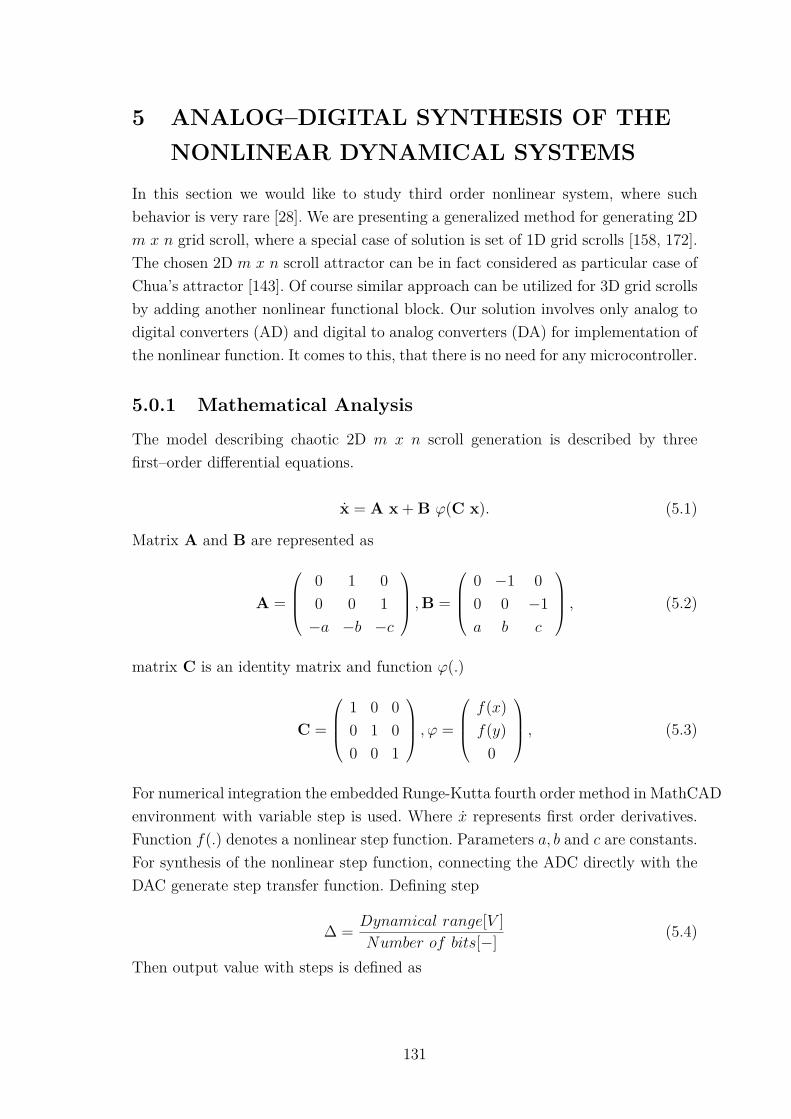
5 ANALOG–DIGITAL SYNTHESIS OF THENONLINEAR DYNAMICAL SYSTEMS
In this section we would like to study third order nonlinear system, where suchbehavior is very rare [28]. We are presenting a generalized method for generating 2D𝑚 𝑥 𝑛 grid scroll, where a special case of solution is set of 1D grid scrolls [158, 172].The chosen 2D 𝑚 𝑥 𝑛 scroll attractor can be in fact considered as particular case ofChua’s attractor [143]. Of course similar approach can be utilized for 3D grid scrollsby adding another nonlinear functional block. Our solution involves only analog todigital converters (AD) and digital to analog converters (DA) for implementation ofthe nonlinear function. It comes to this, that there is no need for any microcontroller.
5.0.1 Mathematical Analysis
The model describing chaotic 2D 𝑚 𝑥 𝑛 scroll generation is described by threefirst–order differential equations.
x = A x + B 𝜙(C x). (5.1)
Matrix A and B are represented as
A =
⎛⎜⎜⎝0 1 00 0 1
−𝑎 −𝑏 −𝑐
⎞⎟⎟⎠ ,B =
⎛⎜⎜⎝0 −1 00 0 −1𝑎 𝑏 𝑐
⎞⎟⎟⎠ , (5.2)
matrix C is an identity matrix and function 𝜙(.)
C =
⎛⎜⎜⎝1 0 00 1 00 0 1
⎞⎟⎟⎠ , 𝜙 =
⎛⎜⎜⎝𝑓(𝑥)𝑓(𝑦)
0
⎞⎟⎟⎠ , (5.3)
For numerical integration the embedded Runge-Kutta fourth order method in MathCADenvironment with variable step is used. Where �� represents first order derivatives.Function 𝑓(.) denotes a nonlinear step function. Parameters 𝑎, 𝑏 and 𝑐 are constants.For synthesis of the nonlinear step function, connecting the ADC directly with theDAC generate step transfer function. Defining step
Δ = 𝐷𝑦𝑛𝑎𝑚𝑖𝑐𝑎𝑙 𝑟𝑎𝑛𝑔𝑒[𝑉 ]𝑁𝑢𝑚𝑏𝑒𝑟 𝑜𝑓 𝑏𝑖𝑡𝑠[−] (5.4)
Then output value with steps is defined as
131

Fig. 5.1: The model of step function 𝑓(𝑥) for 2𝑏 (black) and for 5𝑏 (gray).
𝑜𝑢𝑡(𝑥) =
⎧⎪⎨⎪⎩ł Δ + Δ2 if 𝑥 > 0
𝑙 Δ − Δ2 if 𝑥 < 0,
(5.5)
where
𝑙 = 𝑥
Δ ∧ 𝑙 ∈ N. (5.6)
Where N stands for set of natural numbers. Then model representing ADC connecteddirectly to DAC, the step function with saturation can be written as
𝑓(𝑥) =
⎧⎪⎪⎪⎪⎨⎪⎪⎪⎪⎩𝑜𝑢𝑡(𝑥) if |𝑥| < Ψ−Ψ + Δ
2 if 𝑥 ≤ −ΨΨ − Δ
2 if 𝑥 ≥ Ψ,
(5.7)
where Ψ can be expressed as Ψ = 𝐷𝑦𝑛𝑎𝑚𝑖𝑐𝑎𝑙 𝑟𝑎𝑛𝑔𝑒[𝑉 ]2 .
Such system (5.1) with function (5.7) and with constants set to 𝑎 = 𝑏 = 𝑐 = 0.8can be seen in Fig. 5.2 and Fig. 5.3. Where the both functions (5.7) consists of 4levels. That is equal to utilizing 2 bit AD/DA converters.
5.0.2 Circuitry Realization
To synthesize circuit from differential equations system (5.1), integrator synthesiswas chosen. After thinking about how to reduce the complexity of the nonlinearnetwork a very simple circuitry has been revealed. Only few basic building blocksare necessary: inverting integrators, summing amplifier, AD and DA converters andvoltage sources. Electronic circuit system consists of three integrator circuits (using
132

Fig. 5.2: Numerical simulation of system (5.1), the Monge’s projections 𝑉 (𝑥) vs.𝑉 (𝑦).
Fig. 5.3: Numerical simulation of system (5.1), the Monge’s projections 𝑉 (𝑦) vs.𝑉 (𝑧).
133

R4
C1 C2 C3
R3
R6 R7 R8
R2
R5
R9
R10
R13
R12R11
R14
f(y)
f(x)R1
Fig. 5.4: The block schematics of realization of equations (5.1).
operational amplifier AD713 [189]), which integrate the equations (5.1). Values ofpassive parts are estimated directly from the equations. The circuitry realizationis in Fig. 5.4. In order to ensure Nyquist–Shannon sampling criterion for the con-verters, frequency renormalization is an easy and straightforward process coveringidentical change of all integration constants simultaneously. To create step transferfunctions 𝑓(𝑥) and 𝑓(𝑦), the data converters are used. The schematics in Fig. 5.5shows the data converters connected directly to produce step transfer function. Inorder to process positive and negative voltages, the circuit is divided in the two
A/DROUT
A/D
D/A
D/A
OUTPUT
SYNC
S YNC
S YNCROUT
SYNC
INPUT
Fig. 5.5: The block schematics of realization of function 𝑓(𝑥) using data converters.
134

-2.0V -1.5V -1.0V -0.5V 0.0V 0.5V 1.0V 1.5V 2.0V-2.0V
-1.0V
0V
1.0V
2.0V
Fig. 5.6: The simulations from PSpice program, V(x)versus V(y) projections.
branches. Voltage sources are used as references for the converters. The circuitryrealization was evaluated using PSpice. The overall simulation time is set to 100𝑚𝑠.The simulated output of Monge’s projections is in the Fig. 5.6 to Fig. 5.8. The valuesof passive resistors are 𝑅1 = 𝑅13 = 118 𝑘Ω, 𝑅2 = 𝑅5 = 𝑅9 = 𝑅11 = 𝑅12 = 100 𝑘Ω,𝑅3 = 𝑅4 = 𝑅10 = 125 𝑘Ω, 𝑅6 = 𝑅7 = 𝑅8 = 𝑅14 = 1 𝑘Ω, 𝑅𝑂𝑢𝑡 = 1 Ω and values ofthe capacitors are 𝐶1 = 𝐶2 = 𝐶3 = 100 𝑛𝐹 .
5.0.3 Simulation and Measurement Results
It should be pointed out that hardware implementation of 2D 𝑚 𝑥 𝑛 scroll chaoticattractors is very difficult technically [88] and in [89], despite there is no theoreticallimitation in the mathematical model for generating the large numbers of the multi-dimensional scrolls. The above circuit design method provides a theoretical principlefor hardware implementation of such chaotic attractors with multidirectional orien-tations and a satisfactory number of scrolls. The measurements presented in Fig. 5.9to Fig. 5.14 were done using HP 54645D oscilloscope.
135

-4.0V -3.0V -2.0V -1.0V 0.0V 1.0V 2.0V 3.0V 4.0V-2.0V
-1.0V
0V
1.0V
2.0V
Fig. 5.7: The simulations from PSpice program, V(x)versus V(y) projections.
(A) simulace.dat (active)
-8.0V -6.0V -4.0V -2.0V 0V 2.0V 4.0V 6.0V 8.0V-4.0V
-2.0V
0V
2.0V
4.0V
Fig. 5.8: The simulations from PSpice program, V(x)versus V(y) projections.
136

Fig. 5.9: 1–D 4 scroll. Projections V(x) vs V(-y) (left), V(-y) vs V(z) (right). Hori-zontal axis 1 𝑉/𝑑𝑖𝑣, vertical axis 500𝑚𝑉/𝑑𝑖𝑣 (left), horizontal axis 1 𝑉/𝑑𝑖𝑣, verticalaxis 2 𝑉/𝑑𝑖𝑣 (right).
Fig. 5.10: 1–D 16 scroll. Projections V(x) vs V(-y) (left), V(-y) vs V(z) (right).Horizontal axis 1 𝑉/𝑑𝑖𝑣, vertical axis 500 𝑚𝑉/𝑑𝑖𝑣 (left), horizontal axis 1 𝑉/𝑑𝑖𝑣,vertical axis 500𝑚𝑉/𝑑𝑖𝑣 (right).
Fig. 5.11: Measured system, 2x2 scroll. Projections V(x) vs V(-y) (left), V(-y) vsV(z) (right). Horizontal axis 1 𝑉/𝑑𝑖𝑣, vertical axis 2 𝑉/𝑑𝑖𝑣 (left), horizontal axis1 𝑉/𝑑𝑖𝑣, vertical axis 2 𝑉/𝑑𝑖𝑣 (right).
137

Fig. 5.12: Measured system, 4x4 scroll. Projections V(x) vs V(-y) (left), V(-y) vsV(z) (right). Horizontal axis 1 𝑉/𝑑𝑖𝑣, vertical axis 2 𝑉/𝑑𝑖𝑣 (left), horizontal axis1 𝑉/𝑑𝑖𝑣, vertical axis 2 𝑉/𝑑𝑖𝑣 (right).
Fig. 5.13: Measured system - perturbation of parrameters, 6x4 scroll (left) and 4x2scroll (right). Projections 𝑉 (𝑥) vs. 𝑉 (−𝑦). Horizontal axis 1 𝑉/𝑑𝑖𝑣, vertical axis2 𝑉/𝑑𝑖𝑣 (left), horizontal axis 1 𝑉/𝑑𝑖𝑣, vertical axis 2 𝑉/𝑑𝑖𝑣 (right).
Fig. 5.14: Measured system, 6x6 scroll. Projections 𝑉 (𝑥) vs. 𝑉 (−𝑦) (left), 8x8 scroll,projections 𝑉 (𝑥) vs. 𝑉 (−𝑦) (right). Horizontal axis 1 𝑉/𝑑𝑖𝑣, vertical axis 2 𝑉/𝑑𝑖𝑣(left), horizontal axis 1 𝑉/𝑑𝑖𝑣, vertical axis 2 𝑉/𝑑𝑖𝑣 (right).
138

Fig. 5.15: Numerically simulated 3D (10,10,10) grid scolls.
5.0.4 3D Grid Scrolls
By simple modification of the matrix B and the matrix function 𝜙(.) as follows
B =
⎛⎜⎜⎝0 −1 00 0 −1𝑑 𝑏 𝑐
⎞⎟⎟⎠ , 𝜙 =
⎛⎜⎜⎝𝑓(𝑥)𝑓(𝑦)𝑓(𝑧)
⎞⎟⎟⎠ , (5.8)
one can obtain by setting constant 𝑎 = 𝑏 = 𝑐 = 0.8 and 𝑑 = 0.77 3D (𝑘, 𝑙,𝑚) gridscolls. Where the constant 𝑘, 𝑙,𝑚 stands for the number of levels of the nonlinearity(5.7).
139

5.1 Summary
In this chapter, the well known 2D 𝑚 𝑥 𝑛 scroll system was chosen and was realizedutilizing novel approach using the data converters as non-linear functions. With thegrowing order of the system, the presence of chaotic behavior is more probable. Firstthe models were derived to simulate the data converters connected directly (ADC-DAC). Than the connection was reduced to produce less scrolls. Other crux is in theverify chaotic behavior of proposed conception. The circuit simulator PSpice wasused for theoretical verify and then the circuit prototype was build and measured.
The simulation results and measurements prove a good final agreement betweentheory and practice and were published in[219].
140

6 ON THE POSSIBILITY OF CHAOS DESTRU-CTION VIA PARASITIC PROPERTIES OFTHE USED ACTIVE DEVICES
Anyhow theoretically such analysis can solve problems if desired chaotic pattern isstructurally stable and have potential for the practical applications. If such stabilitycan not be satisfied to some degree the desired chaotic attractor is not experimentallyobservable.
Common worst-case analysis is probably not a correct approach to determinestructural stability of the state space attractors in the case of the nonlinear vectorfield since largest LE is not a monotonic function of the parasitic elements. In otherwords crucial perturbation of the flow can not necessarily appear for the bordervalues of the combined parasitic properties. It seems that largest LE should be pro-vided in a hyper–dimensional tabularized fashion. It is evident that it is impossibleto consider the parasitic properties of the individual active devices separately; bothfrom the viewpoint of confusing visualization and enormous time demands requiredfor calculation. Thus to quantify the influence of the non–ideal properties of theactive devices on the desired strange attractors a term generalized parasitic can beintroduced. It means that parasitic effects which have the same nature are appliedon the mathematical model of chaotic oscillator together. The simplest such gene-ralized parasitic effects are additional dissipation, parameters uncertainty and lossintegration. Positive largest LE indicates a system solution which is sensitive to thechanges of the initial conditions while zero value denotes a limit cycle (no matterhow complex it looks like).
Parasitic properties of the active devices have accumulating tendencies; it meansthat one basic error term is not generally compensated by the other. In OTA basedrealizations parasitic capacitor which belongs to the input impedance is connected inparallel with working one and enlarges time constant. Input resistance is responsiblefor increased dissipation of dynamical flow; if this property crosses critical value a de-sired strange attractor collapse into the simpler geometrical structure, i.e. limit cycleor, if dissipation is extremely strong, a fixed point. In CCII based oscillators inputresistance of X-terminal is connected in series with working resistor causing againa time constant enlargement effect. Roll–off effect of each OTA transconductanceas well as each CCII current transfer constant also has a devastating impact on thedesired state attractor.
Since chaotic solution is usually surrounded in hyperspace of internal systemparameters by unbounded solution strange attractor often collapses into large limitcycle with squared quasi–radius defined by the saturation levels of the used active
141

devices.This part deals with the study of influences of input and output parasitic proper-
ties of used real active elements. It is very interesting thing, because chaos systemsare very sensitive on initial condition and values of circuit elements which should bekept very precisely. From this point of view it is very important to deal with question,whether parasitic properties are critical for system function and how global behaviorchanges with some sort of uncertainty. The question is whether or not these parasiticelements can cause significant problems in formation of the state space and chaosdestruction in the worst case. The impact of the parasitic properties is to be takeninto account during the system design. Performances of the proposed circuits fromprevious chapters are confirmed through numerical analysis and PSpice simulationswith consideration influence of parasitic properties of active elements. This part alsodeals with mathematical analysis and calculations of eigenvalues with thinking ofinfluences of active elements parasitics.
6.1 Influences of Active Elements Parasitics
Non–ideal active elements are depicted in Fig. 6.1 resp. Fig. 6.2. Parasitic analysisdeals mainly with input and output properties of used active element that causesignificant problems in the state space. Important parasitic admittances of the circuit(signed as 𝑌𝑝) are caused by the real input and output properties of used activeelements. Common input and output small signal parameters for OTA (OPA860) are𝑅𝑖𝑛_𝑂𝑇 𝐴 = 455𝑘Ω, 𝑅𝑜𝑢𝑡_𝑂𝑇 𝐴 = 54𝑘Ω, 𝐶𝑖𝑛_𝑂𝑇 𝐴 = 2.2𝑝𝐹 , 𝐶𝑜𝑢𝑡_𝑂𝑇 𝐴 = 2𝑝𝐹 , for OTA(AD844) are 𝑅𝑖𝑛_𝑂𝑇 𝐴 = 10 𝑀Ω, 𝑅𝑜𝑢𝑡_𝑂𝑇 𝐴 = 3 𝑀Ω, 𝐶𝑖𝑛_𝑂𝑇 𝐴 = 2 𝑝𝐹 , 𝐶𝑜𝑢𝑡_𝑂𝑇 𝐴 =4.5𝑝𝐹 and for MO-OTA (MAX435) are 𝑅𝑖𝑛_𝑀𝑂𝑂𝑇 𝐴 = 800𝑘Ω, 𝑅𝑜𝑢𝑡_𝑀𝑂𝑂𝑇 𝐴 = 3.5𝑘Ω,𝐶𝑖𝑛_𝑀𝑂𝑂𝑇 𝐴 = 4 𝑝𝐹 , 𝐶𝑜𝑢𝑡_𝑀𝑂𝑂𝑇 𝐴 = 4.1 𝑝𝐹 .
Rin_OTA Rout_OTAgmVi
Cin_OTA Cout_OTA
Ii
Vi
I0
Fig. 6.1: Non-ideal model of operational transconductance amplifier (OTA).
142

Cout_MOOT A
Rout_MOOT AgmVi
Ii
Rout_MOOT A
Vi
+I0
Cin_MOOT A
Cout_MOOT A
Rout_MOOT A-gmVi
-I0
Fig. 6.2: Non-ideal model of multiple output operational transconductance amplifier(MO-OTA).
6.2 Influence of Parasitic Properties of Active Ele-ments in Circuit Based on Inertia Neuron Mo-del
In this section are discussed influences of parasitic properties of active elementsin system based on inertia neuron model described in the previous subchaptersection 4.3. We suppose three locations (input and output admittances in three no-des) where is the highest impact of parasitic properties. These parasitic admittancesare described by a following set of the equations
𝑌𝑝1(𝑠) = 𝐺𝑝1 + 𝑠𝐶𝑝1, (6.1)
𝑌𝑝2(𝑠) = 𝐺𝑝2 + 𝑠𝐶𝑝2, (6.2)
𝑌𝑝3(𝑠) = 𝐺𝑝3 + 𝑠𝐶𝑝3. (6.3)
The relations between inertia neuron model and parasitic admittances are given bythe formulas
−(𝐶1 + 𝐶𝑝1)𝑑𝑢1𝑑𝑡
= 𝑢2 + 𝑎𝑢12 − 𝑢1
2 − 𝑢3 + 𝐼 −𝐺𝑝1𝑢1
−(𝐶2 + 𝐶𝑝2)𝑑𝑢2𝑑𝑡
= 1 −𝐷𝑢12 − 𝑢2 −𝐺𝑝2𝑢2
−(𝐶3 + 𝐶𝑝3)𝑑𝑢3𝑑𝑡
= 𝜇 (𝑏 (𝑢1 − 𝑥0) − 𝑢3) −𝐺𝑝3𝑢3.
(6.4)
−𝑑𝑢1𝑑𝑡
= 𝑢2+𝑎𝑢12−𝑢12−𝑢3+𝐼−𝐺𝑝1𝑢1𝐶1+𝐶𝑝1
−𝑑𝑢2𝑑𝑡
= 1−𝐷𝑢12−𝑢2−𝐺𝑝2𝑢2𝐶2+𝐶𝑝2
−𝑑𝑢3𝑑𝑡
= 𝜇(𝑏(𝑢1−𝑥0)−𝑢3)−𝐺𝑝3𝑢3𝐶3+𝐶𝑝3
,
(6.5)
143

Fig. 6.3: Influence of parasitic capaci-tances on the size of the 𝐿𝐸𝑚𝑎𝑥 as afunction of 𝐶𝑝1 and 𝐶𝑝2.
Fig. 6.4: Influence of parasitic capaci-tances on the size of the 𝐿𝐸𝑚𝑎𝑥 as afunction of 𝐶𝑝1 and 𝐶𝑝3.
Fig. 6.5: Influence of parasitic capaci-tances on the size of the 𝐿𝐸𝑚𝑎𝑥 as afunction of 𝐶𝑝2 and 𝐶𝑝3.
Fig. 6.6: Influence of parasitic con-ductances on the size of the 𝐿𝐸𝑚𝑎𝑥
as a function of 𝐺𝑝1 and 𝐺𝑝2.
Fig. 6.7: Influence of parasitic con-ductances on the size of the 𝐿𝐸𝑚𝑎𝑥
as a function of 𝐺𝑝1 and 𝐺𝑝3.
Fig. 6.8: Influence of parasitic con-ductances on the size of the 𝐿𝐸𝑚𝑎𝑥
as a function of 𝐺𝑝2 and 𝐺𝑝3.
144

As was mentioned in the previous subchapter (1.2.1) to obtain sensitivity to theinitial conditions (chaos) it is necessary to have one LE positive. From the viewpointof chaos destruction has been calculated the largest Lyapunov exponents (𝐿𝐸𝑚𝑎𝑥)which are indicated the possible occurance of chaos. Working capacitances were seton the normative value equal to 1. The positive 𝐿𝐸𝑚𝑎𝑥 dependence on values ofparasitic properties are shown in Fig. 6.3 to Fig. 6.8 using the 3D contour plot withscale 𝐿𝐸𝑚𝑎𝑥 ∈ (−0.01, 0.01). Although full graph should be many–dimensional onlytwo nonidealities are considered for each graph. This contour plots of the 𝐿𝐸𝑚𝑎𝑥
have the axis resolution 𝑋 = 𝑌 = 30 values uncovering how the structure of thechaotic attractor is sensitive to the changes of parasitic properties. The numericalanalysis involving the computation of the 𝐿𝐸𝑚𝑎𝑥 reveals that the chaotic regionsare significantly surrounded by the regions with unbounded solution. If the parasiticproperties are growing up the 𝐿𝐸𝑚𝑎𝑥 becomes negative. It is indicating the impossi-ble occurance of chaos for this interval of parameters. Therefore it is evident thatthe most common solution of the system with influence of parasitic properties is alimit cycle. On the other side when the values of parasitic properties convert to zerothe positive value of 𝐿𝐸𝑚𝑎𝑥 is indicating the possible occurance of chaos.
145

6.3 Influence of Parasitic Properties of Active Ele-ments in Circuit Based on Memristor Proper-ties
In Fig. 6.1 the suitable model of the real OTA which includes the most importantparasitic parameters is given. Then using this model (Fig. 6.1) the circuit diagramfrom Fig. 4.64 can be supplemented as shown in Fig. 6.9 to include all parasiticinfluences. Elementswith crosshatch pattern are representing parasitic influences.We suppose three locations (input and output admittances in three nodes) where isthe highest impact of parasitic properties. These parasitic admittances (see Fig. 6.9)are expressed
gm3
gm1
C1 C2 C3
Y Z
R3
X
gm2
X1
X2
Y1
Y2
Z
WR2
X1
X2
Y1
Y2
Z
WR1
ISET1
ISET2
ISET3
Gp1 Gp2 Gp3
Fig. 6.9: Circuit realization of the chaotic system with influence of parasitic proper-ties of active elements.
𝑌𝑝1(𝑠) = 𝐺𝑝1 + 𝑠𝐶𝑝1 = (𝐺𝑝𝑖𝑛2 +𝐺𝑝𝑜𝑢𝑡3)++ 𝑠(𝐶𝑝𝑖𝑛1 + 𝐶𝑝𝑜𝑢𝑡3) =
= 1𝑅𝑖𝑛_𝑂𝑇 𝐴2
+ 1𝑅𝑜𝑢𝑡_𝑀𝑂𝑂𝑇 𝐴
+ 𝑠 (𝐶𝑖𝑛_𝑂𝑇 𝐴1 + 𝐶𝑜𝑢𝑡_𝑀𝑂𝑂𝑇 𝐴) ,(6.6)
146

𝑌𝑝2(𝑠) = 𝐺𝑝2 + 𝑠𝐶𝑝2 = (𝐺𝑝𝑖𝑛1 +𝐺𝑝𝑖𝑛3 +𝐺𝑝𝑜𝑢𝑡1 +𝐺𝑝𝑜𝑢𝑡2)+ 𝑠(𝐶𝑝𝑖𝑛1 + 𝐶𝑝𝑖𝑛3 + 𝐶𝑝𝑜𝑢𝑡1 + 𝐶𝑝𝑜𝑢𝑡2) =
= 1𝑅𝑖𝑛_𝑂𝑇 𝐴1
+ 1𝑅𝑖𝑛_𝑀𝑂𝑂𝑇 𝐴
+ 1𝑅𝑜𝑢𝑡_𝑂𝑇 𝐴1
+ 1𝑅𝑜𝑢𝑡_𝑂𝑇 𝐴2
+
+ 𝑠(𝐶𝑖𝑛_𝑂𝑇 𝐴1 + 𝐶𝑖𝑛_𝑀𝑂𝑂𝑇 𝐴 + 𝐶𝑜𝑢𝑡_𝑂𝑇 𝐴1 + 𝐶𝑜𝑢𝑡_𝑂𝑇 𝐴2),
(6.7)
𝑌𝑝3(𝑠) = 𝐺𝑝3 + 𝑠𝐶𝑝3 = 𝐺𝑝𝑜𝑢𝑡3 + 𝑠𝐶𝑝𝑜𝑢𝑡3 =
= 1𝑅𝑜𝑢𝑡_𝑀𝑂𝑂𝑇 𝐴
+ 𝑠𝐶𝑜𝑢𝑡_𝑀𝑂𝑂𝑇 𝐴.(6.8)
The relations between ideal model and parasitic admittances are given by the for-mulas
−(𝐶1 + 𝐶𝑝1)𝑑𝑢1𝑑𝑡
= 𝐺𝑝1𝑢1 − 𝑔𝑚3𝑢2
−(𝐶2 + 𝐶𝑝2)𝑑𝑢2𝑑𝑡
= 13𝑔𝑚2𝑢1 − (1
2𝑔𝑚1 −𝐺𝑝2)𝑢2 + 12𝑢2𝑢3
2
−(𝐶3 + 𝐶𝑝3)𝑑𝑢3𝑑𝑡
= 𝑔𝑚3𝑢2 + (𝐺+𝐺𝑝3)𝑢3 − 𝑢2𝑢3
(6.9)
−𝑑𝑢1𝑑𝑡
= 𝐺𝑝1𝑢1−𝑔𝑚3𝑢2𝐶1+𝐶𝑝1
−𝑑𝑢2𝑑𝑡
=13 𝑔𝑚2𝑢1−( 1
2 𝑔𝑚1−𝐺𝑝2)𝑢2+ 12 𝑢2𝑢32
𝐶2+𝐶𝑝2
−𝑑𝑢3𝑑𝑡
= 𝑔𝑚3𝑢2+(𝐺+𝐺𝑝3)𝑢3−𝑢2𝑢3𝐶3+𝐶𝑝3
(6.10)
𝐺𝑝1 = 1𝑅𝑖𝑛_𝑂𝑇 𝐴2
+ 1𝑅𝑜𝑢𝑡_𝑀𝑂𝑂𝑇 𝐴
, 𝐺𝑝3 = 1𝑅𝑜𝑢𝑡_𝑀𝑂𝑂𝑇 𝐴
(6.11)
𝐺𝑝2 = 1𝑅𝑖𝑛_𝑂𝑇 𝐴1
+ 1𝑅𝑖𝑛_𝑀𝑂𝑂𝑇 𝐴
+ 1𝑅𝑜𝑢𝑡_𝑂𝑇 𝐴1
+ 1𝑅𝑜𝑢𝑡_𝑂𝑇 𝐴2
(6.12)
𝐶𝑝1 = 𝐶𝑖𝑛_𝑂𝑇 𝐴1 + 𝐶𝑜𝑢𝑡_𝑀𝑂𝑂𝑇 𝐴, 𝐶𝑝3 = 𝐶𝑜𝑢𝑡_𝑀𝑂𝑂𝑇 𝐴 (6.13)
𝐶𝑝2 = 𝐶𝑖𝑛_𝑂𝑇 𝐴1 + 𝐶𝑖𝑛_𝑀𝑂𝑂𝑇 𝐴 + 𝐶𝑜𝑢𝑡_𝑂𝑇 𝐴1 + 𝐶𝑜𝑢𝑡_𝑂𝑇 𝐴2 (6.14)
The concrete values of the parasitic admitances of the developed circuitry shown inFig. 6.9 are for OTA (OPA860) 𝑅𝑖𝑛_𝑂𝑇 𝐴 = 455 𝑘Ω, 𝑅𝑜𝑢𝑡_𝑂𝑇 𝐴 = 54 𝑘Ω, 𝐶𝑖𝑛_𝑂𝑇 𝐴 =2.2 𝑝𝐹 , 𝐶𝑜𝑢𝑡_𝑂𝑇 𝐴 = 2 𝑝𝐹 and for MO-OTA (MAX435) are 𝑅𝑖𝑛_𝑀𝑂𝑂𝑇 𝐴 = 800 𝑘Ω,𝑅𝑜𝑢𝑡_𝑀𝑂𝑂𝑇 𝐴 = 3.5 𝑘Ω, 𝐶𝑖𝑛_𝑀𝑂𝑂𝑇 𝐴 = 4 𝑝𝐹 , 𝐶𝑜𝑢𝑡_𝑀𝑂𝑂𝑇 𝐴 = 4.1 𝑝𝐹 . Results of nu-merical analysis with influence of parasitic elements are shown in Fig. 6.10. Thepositive 𝐿𝐸𝑚𝑎𝑥 dependence on values of parasitic properties are shown in Fig. 6.11
147

Fig. 6.10: Numerical analysis of system with memristor properties and influence ofparasitic elements - projection X-Y (red-with parasitic, blue-without parasitic).
to Fig. 6.18 with scale 𝐿𝐸𝑚𝑎𝑥 ∈ (0, 0.04). Capacitances 𝐶1, = 𝐶2, = 𝐶3 used innumerical analysis have normative values 1. Contour plots of the 𝐿𝐸𝑚𝑎𝑥 have theaxis resolution 𝑋 = 𝑌 = 30 values. As is evident from plots Fig. 6.11 to Fig. 6.18circuitry is much more sensitive to the changes of the parasitic conductances thanthe parasitic capacitances. The influence of the parasitic capacitance will be appliedin cases when their value will be close to the value of working capacitances. Theconclusion is that at high frequencies, the values of the parasitic capacitances arecomparable to those of other circuit elements and thus the resulted behavior of thecircuit is unpredictable.
LEmax
0.01
0.02
0.03
0.04
GoutOTA
0
0.10.1
0
0.05GinOTA0.05
0.10.2
LEmax
0.01
0.02
0.03
0.04
GoutMOTA
0
0.150.3
0
0.1
GinMOTA
0.05
0
Fig. 6.11: Influence of parasitic con-ductances on the size of the 𝐿𝐸𝑚𝑎𝑥 asa function of OPA860 parasitic con-ductance.
Fig. 6.12: Influence of parasitic con-ductances on the size of the 𝐿𝐸𝑚𝑎𝑥 asa function of MAX435 parasitic con-ductance.
148

0.10.20.1
LEmax
0.01
0.02
0.03
0.04
GinMOTA
0
0.10.15
0
0.05
GinOTA0.05
0
0.10.20.10.2
LEmax
0.01
0.02
0.03
0.04
GoutMOTA
0
0.10.3
0
0.1
GoutOTA0.05
0
Fig. 6.13: Influence of parasitic con-ductances on the size of the 𝐿𝐸𝑚𝑎𝑥 asa function of OPA860 and MAX435input parasitic conductances.
Fig. 6.14: Influence of parasitic con-ductances on the size of the 𝐿𝐸𝑚𝑎𝑥 asa function of OPA860 and MAX435output parasitic conductances.
LEmax
0
0.02
0.04
1
0.5
CinOTA1
0.5
CoutOTA
LEmax
0.01
0.02
0.03
0.04
CoutMOTA
0.5
0
221.5 1.5
0.51
CinMOTA1
Fig. 6.15: Influence of parasitic capa-citances on the size of the 𝐿𝐸𝑚𝑎𝑥 as afunction of OPA860 parasitic capaci-tance.
Fig. 6.16: Influence of parasitic capa-citances on the size of the 𝐿𝐸𝑚𝑎𝑥 as afunction of MAX435 parasitic capaci-tance.
LEmax
0.02
0.04
CinMOTA
0.5
0
221.5 1.5
0.51
CinOTA1
LEmax
0.01
0.02
0.03
0.04
CoutMOTA
0.5
0
231.5
1
2 CoutOTA1
Fig. 6.17: Influence of parasitic capa-citances on the size of the 𝐿𝐸𝑚𝑎𝑥 asa function of OPA860 and MAX435input parasitic capacitances.
Fig. 6.18: Influence of parasitic capa-citances on the size of the 𝐿𝐸𝑚𝑎𝑥 asa function of OPA860 and MAX435output parasitic capacitances.
149

6.3.1 Calculation of Eigenvalues
Now we will consider a new form of the system (6.9), where state matrix 𝐴𝑝 isrepresented influence of the parasitic conductances of the active elements.
x = (A + A𝑝)𝑥+ B𝑥𝑥𝑇 C + D𝑥(𝑥𝑇 C
)2(6.15)
A =
⎛⎜⎜⎝0 𝑔𝑚3 0
−13 · 𝑔𝑚2
12 · 𝑔𝑚1 0
0 −𝑔𝑚3 −0.6
⎞⎟⎟⎠ , (6.16)
A𝑝 =
⎛⎜⎜⎝−𝐺𝑝1 0 0
0 −𝐺𝑝2 00 0 −𝐺𝑝3
⎞⎟⎟⎠ , (6.17)
B =
⎛⎜⎜⎝0 0 00 0 00 1 0
⎞⎟⎟⎠ , C =
⎛⎜⎜⎝001
⎞⎟⎟⎠ (6.18)
D =
⎛⎜⎜⎝0 0 00 −1
2 00 0 0
⎞⎟⎟⎠ , (6.19)
The Jacobian matrix and the local behavior of the system (6.10) near the originwith influence of parasitic properties of active elements is
J𝑝 =
⎛⎜⎜⎝−𝐺𝑝1 1 0−1
3 −12𝑧
2 + 12 −𝐺𝑝2 −𝑦𝑧
0 𝑧 − 1 𝑦 − 0.6 −𝐺𝑝3
⎞⎟⎟⎠ (6.20)
and characteristic polynomial for critical point (0, 0, 0) is following
𝑑𝑒𝑡(𝜆I − J𝑝) == 𝜆3 + 1.714𝜆2 + 1.223𝜆+ 0.433 = 0.
(6.21)
New values of eigenvalues are
𝜆4,5 = 0.086 ± 0.44𝑖 𝜆6 = −0.886. (6.22)
150

6.4 Influence of Parasitic Properties of Active Ele-ments in Circuit Based on Sprott system
Consider same algebraically simple three-dimensional ODEs with six terms and onenonlinearity (4.29) as was mentioned in subchapter section 4.5. In Fig. 6.1, resp.Fig. 6.2 the suitable models of the real OTA and MO-OTA which includes the mostimportant parasitic parameters are given. Then using this model (Fig. 6.1, Fig. 6.2)the circuit diagram from Fig. 4.34 can be supplemented as shown in Fig. 6.19 toinclude all parasitic influences. Elementswith crosshatch pattern are representingparasitic influences. In circuit realization (Fig. 6.19) we suppose four locations (twonodes and two input diferences admittance) where parasitics cause the highest im-pact. These parasitic admittances can be expressed as
gm3
C1 C2 C3
gm1
gm2
X Y Z
x.z
G Yp1
Yp2
Yp4
Yp3
Fig. 6.19: Schematic of circuit realization with important parasitic influences.
𝑌𝑝1(𝑠) = 𝐺𝑝1 + 𝑠𝐶𝑝1 = (𝐺𝑝𝑖𝑛1 +𝐺𝑝𝑜𝑢𝑡1++𝐺𝑝𝑜𝑢𝑡3) + 𝑠(𝐶𝑝𝑖𝑛1 + 𝐶𝑝𝑜𝑢𝑡1 + 𝐶𝑝𝑜𝑢𝑡3) =
= 1𝑅𝑖𝑛_𝑂𝑇 𝐴1
+ 1𝑅𝑜𝑢𝑡_𝑂𝑇 𝐴1
+ 1𝑅𝑜𝑢𝑡_𝑂𝑇 𝐴3
+
+ 𝑠 (𝐶𝑖𝑛_𝑂𝑇 𝐴1 + 𝐶𝑜𝑢𝑡_𝑂𝑇 𝐴1 + 𝐶𝑜𝑢𝑡_𝑂𝑇 𝐴3)
(6.23)
𝑌𝑝2(𝑠) = 𝐺𝑝2 + 𝑠𝐶𝑝2 = 𝐺𝑝𝑜𝑢𝑡2 + 𝑠𝐶𝑝𝑜𝑢𝑡2 =
= 1𝑅𝑜𝑢𝑡_𝑂𝑇 𝐴2
+ 𝑠𝐶𝑜𝑢𝑡_𝑂𝑇 𝐴2
(6.24)
151

𝑌𝑝3(𝑠) = 𝐺𝑝3 + 𝑠𝐶𝑝𝑝3 = 𝐺𝑝𝑖𝑛3 + 𝑠𝐶𝑖𝑛3 = 1𝑅𝑖𝑛_𝑂𝑇 𝐴3
+ 𝑠𝐶𝑖𝑛_𝑂𝑇 𝐴3 (6.25)
𝑌𝑝4(𝑠) = 𝐺𝑝4 + 𝑠𝐶𝑝𝑝4 = 𝐺𝑝𝑖𝑛2 + 𝑠𝐶𝑖𝑛2 = 1𝑅𝑖𝑛_𝑂𝑇 𝐴2
+ 𝑠𝐶𝑖𝑛_𝑂𝑇 𝐴2 (6.26)
−(𝐶1 + 𝐶𝑝1)𝑑𝑢1
𝑑𝑡= (𝑔𝑚1 − 𝑔𝑚3 −𝐺𝑝1 −𝐺𝑝3 −𝐺𝑝4)𝑢1 +𝐺𝑝4𝑢2 + (𝑔𝑚3 +𝐺𝑝3)𝑢3−
− 𝐶𝑝𝑝3𝑑𝑢3
𝑑𝑡+ 𝐶𝑝𝑝3
𝑑𝑢1
𝑑𝑡− 𝐶𝑝𝑝4
𝑑𝑢2
𝑑𝑡+ 𝐶𝑝𝑝4
𝑑𝑢1
𝑑𝑡
−𝐶2𝑑𝑢2
𝑑𝑡=𝐺𝑝4𝑢1 − (𝐺+𝐺𝑝4)𝑢2 + 𝑢1𝑢3 + 𝐶𝑝𝑝4
𝑑𝑢2
𝑑𝑡− 𝐶𝑝𝑝4
𝑑𝑢1
𝑑𝑡
−(𝐶3 + 𝐶𝑝2)𝑑𝑢3
𝑑𝑡= (−𝑔𝑚2 +𝐺𝑝3)𝑢1 + 𝑔𝑚2𝑢2 − (𝐺𝑝2 +𝐺𝑝3)𝑢3 − 𝐶𝑝𝑝3
𝑑𝑢1
𝑑𝑡+
+ 𝐶𝑝𝑝3𝑑𝑢3
𝑑𝑡(6.27)
−𝑑𝑢1
𝑑𝑡= (𝑔𝑚1 − 𝑔𝑚3 −𝐺𝑝1 −𝐺𝑝3 −𝐺𝑝4)𝑢1
𝐶1 + 𝐶𝑝1+ 𝐶𝑝𝑝3(−𝑔𝑚2 +𝐺𝑝3)𝑢1
𝐶3 + 𝐶𝑝2+
+ 𝐶𝑝𝑝3(𝑔𝑚1 − 𝑔𝑚3 −𝐺𝑝1 −𝐺𝑝3 −𝐺𝑝4)𝑢1
𝐶1 + 𝐶𝑝1− 𝐶𝑝𝑝4𝐺𝑝4𝑢1
𝐶2+
+ 𝐶𝑝𝑝4(𝑔𝑚1 − 𝑔𝑚3 −𝐺𝑝1 −𝐺𝑝3 −𝐺𝑝4)𝑢1
𝐶1 + 𝐶𝑝1+ 𝐺𝑝4𝑢2
𝐶1 + 𝐶𝑝1− 𝐶𝑝𝑝3𝑔𝑚2𝑢2
𝐶3 + 𝐶𝑝2+
+ 𝐶𝑝𝑝3𝐺𝑝4𝑢2
𝐶1 + 𝐶𝑝1+ 𝐶𝑝𝑝4(𝐺+𝐺𝑝4)𝑢2
𝐶2+ 𝐶𝑝𝑝4𝐺𝑝4𝑢2
𝐶1 + 𝐶𝑝1+ (𝑔𝑚3 +𝐺𝑝3)𝑢3
𝐶1 + 𝐶𝑝1+
+ 𝐶𝑝𝑝3(𝐺𝑝2 +𝐺𝑝3)𝑢3
𝐶3 + 𝐶𝑝2+ 𝐶𝑝𝑝3(𝑔𝑚3 +𝐺𝑝3)𝑢3
𝐶1 + 𝐶𝑝1+ 𝐶𝑝𝑝4(𝑔𝑚3 +𝐺𝑝3)𝑢3
𝐶1 + 𝐶𝑝1− 𝐶𝑝𝑝4𝑢1𝑢3
𝐶2
−𝑑𝑢2
𝑑𝑡= 𝐺𝑝4𝑢1
𝐶2− 𝐶𝑝𝑝4𝐺𝑝4𝑢1
𝐶2− 𝐶𝑝𝑝4(𝑔𝑚1 − 𝑔𝑚3 −𝐺𝑝1 −𝐺𝑝3 −𝐺𝑝4)𝑢1
𝐶1 + 𝐶𝑝1−
− (𝐺+𝐺𝑝4)𝑢2
𝐶2− 𝐶𝑝𝑝4(𝐺+𝐺𝑝4)𝑢2
𝐶2− 𝐶𝑝𝑝4𝐺𝑝4𝑢2
𝐶1 + 𝐶𝑝1− 𝐶𝑝𝑝4(𝑔𝑚3 +𝐺𝑝3)𝑢3
𝐶1 + 𝐶𝑝1+
+ 𝑢1𝑢3
𝐶2+ 𝐶𝑝𝑝4𝑢1𝑢3
𝐶2
−𝑑𝑢3
𝑑𝑡= (−𝑔𝑚2 +𝐺𝑝3)𝑢1
𝐶3 + 𝐶𝑝2+ 𝐶𝑝𝑝3(𝑔𝑚1 − 𝑔𝑚3 −𝐺𝑝1 −𝐺𝑝3 −𝐺𝑝4)𝑢1
𝐶1 + 𝐶𝑝1−
− 𝐶𝑝𝑝3(−𝑔𝑚2 +𝐺𝑝3)𝑢1
𝐶3 + 𝐶𝑝2+ 𝑔𝑚2𝑢2
𝐶3 + 𝐶𝑝2+ 𝐶𝑝𝑝3𝐺𝑝4𝑢2
𝐶1 + 𝐶𝑝1− 𝐶𝑝𝑝3𝑔𝑚2𝑢2
𝐶3 + 𝐶𝑝2−
− (𝐺𝑝2 +𝐺𝑝3)𝑢3
𝐶3 + 𝐶𝑝2+ 𝐶𝑝𝑝3(𝐺𝑝2 +𝐺𝑝3)𝑢3
𝐶3 + 𝐶𝑝2+ 𝐶𝑝𝑝3(𝑔𝑚3 +𝐺𝑝3)𝑢3
𝐶1 + 𝐶𝑝1
(6.28)
The concrete values of the parasitic admitances of the developed circuitry shownin Fig. 6.19 are for OTA (OPA860) 𝑅𝑖𝑛_𝑂𝑇 𝐴 = 455𝑘Ω, 𝑅𝑜𝑢𝑡_𝑂𝑇 𝐴 = 54𝑘Ω, 𝐶𝑖𝑛_𝑂𝑇 𝐴 =2.2 𝑝𝐹 , 𝐶𝑜𝑢𝑡_𝑂𝑇 𝐴 = 2 𝑝𝐹 .
152

Fig. 6.20: Numerical analysis with influence of parasitic elements - projection X-Y(red - with parasitic, blue - without parasitic).
𝐺𝑝1 = 1𝑅𝑖𝑛_𝑂𝑇 𝐴
+ 1𝑅𝑜𝑢𝑡_𝑂𝑇 𝐴
+ 1𝑅𝑜𝑢𝑡_𝑂𝑇 𝐴
(6.29)
𝐺𝑝2 = 1𝑅𝑜𝑢𝑡_𝑂𝑇 𝐴
, 𝐺𝑝3 = 1𝑅𝑖𝑛_𝑂𝑇 𝐴
, 𝐺𝑝4 = 1𝑅𝑖𝑛_𝑂𝑇 𝐴
(6.30)
𝐶𝑝1 = 𝐶𝑖𝑛_𝑂𝑇 𝐴 + 𝐶𝑜𝑢𝑡_𝑂𝑇 𝐴 + 𝐶𝑜𝑢𝑡_𝑂𝑇 𝐴 (6.31)
𝐶𝑝2 = 𝐶𝑜𝑢𝑡_𝑂𝑇 𝐴, 𝐶𝑝𝑝3 = 𝐶𝑖𝑛_𝑂𝑇 𝐴, 𝐶𝑝𝑝4 = 𝐶𝑖𝑛_𝑂𝑇 𝐴 (6.32)
Values of used passive elements in schematic in Fig. 6.19 were chosen same as inprevious chapter (𝐶1 = 𝐶2 = 𝐶3 = 470 𝑛𝐹, 𝑅 = 1 𝑘Ω). Results of numerical analysiswith influence of parasitic elements are shown in Fig. 6.20. Influences of parasiticproperties were simulated also in PSpice and the results of the simulations are shownin Fig. 6.21. The positive 𝐿𝐸𝑚𝑎𝑥 dependence on values of parasitic properties areshown in Fig. 6.22 to Fig. 6.37 with scale 𝐿𝐸𝑚𝑎𝑥 ∈ (0, 0.01). Capacitances 𝐶1, =𝐶2, = 𝐶3 used in numerical analysis have again normative values 1. Contour plotsof the 𝐿𝐸𝑚𝑎𝑥 have the axis resolution 𝑋 = 𝑌 = 30 values. Circuit has the similarproperties as in previuous case with memristor properties. Sensitivity to change ofthe parasitic conductances is bigger than the sensitivity to the changes of parasiticcapacitances. The most critical to chaos destruction seems to be parasitic outputresistance of the MO-OTA element MAX435 with value approaching the workingresistance.
153

-V(z)
-3.0V -2.0V -1.0V 0V 1.0V 2.0V 3.0VV(x)
-3.0V
-2.0V
-1.0V
0V
1.0V
2.0V
-V(z)
-3.0V -2.0V -1.0V 0V 1.0V 2.0V 3.0VV(x)
-3.0V
-2.0V
-1.0V
0V
1.0V
2.0V
Fig. 6.21: Circuit simulation with influence of parasitic elements (left - with parasitic,right - with parasitic compensate ).
Fig. 6.22: Influence of parasitic capa-citances on the size of the 𝐿𝐸𝑚𝑎𝑥 as afunction of 𝐶𝑝1 and 𝐶𝑝2.
Fig. 6.23: Influence of parasitic capa-citances on the size of the 𝐿𝐸𝑚𝑎𝑥 as afunction of 𝐶𝑝1 and 𝐶𝑝𝑝3.
Fig. 6.24: Influence of parasitic capa-citances on the size of the 𝐿𝐸𝑚𝑎𝑥 as afunction of 𝐶𝑝1 and 𝐶𝑝𝑝4.
Fig. 6.25: Influence of parasitic capa-citances on the size of the 𝐿𝐸𝑚𝑎𝑥 as afunction of 𝐶𝑝2 and 𝐶𝑝𝑝3.
154

Fig. 6.26: Influence of parasitic capa-citances on the size of the 𝐿𝐸𝑚𝑎𝑥 as afunction of 𝐶𝑝2 and 𝐶𝑝𝑝4.
Fig. 6.27: Influence of parasitic capa-citances on the size of the 𝐿𝐸𝑚𝑎𝑥 as afunction of 𝐶𝑝𝑝3 and 𝐶𝑝𝑝4.
Fig. 6.28: Influence of parasitic con-ductances on the size of the 𝐿𝐸𝑚𝑎𝑥 asa function of 𝐺𝑝1 and 𝐺𝑝2.
Fig. 6.29: Influence of parasitic con-ductances on the size of the 𝐿𝐸𝑚𝑎𝑥 asa function of 𝐺𝑝1 and 𝐺𝑝3.
Fig. 6.30: Influence of parasitic con-ductances on the size of the 𝐿𝐸𝑚𝑎𝑥 asa function of 𝐺𝑝1 and 𝐺𝑝4.
Fig. 6.31: Influence of parasitic con-ductances on the size of the 𝐿𝐸𝑚𝑎𝑥 asa function of 𝐺𝑝2 and 𝐺𝑝3.
155

Fig. 6.32: Influence of parasitic con-ductances on the size of the 𝐿𝐸𝑚𝑎𝑥 asa function of 𝐺𝑝2 and 𝐺𝑝4.
Fig. 6.33: Influence of parasitic con-ductances on the size of the 𝐿𝐸𝑚𝑎𝑥 asa function of 𝐺𝑝3 and 𝐺𝑝4.
Fig. 6.34: Influence of parasitic con-ductance and capacitance on the sizeof the 𝐿𝐸𝑚𝑎𝑥 as a function of 𝐺𝑝1 and𝐶𝑝1.
Fig. 6.35: Influence of parasitic con-ductance and capacitance on the sizeof the 𝐿𝐸𝑚𝑎𝑥 as a function of 𝐺𝑝2 and𝐶𝑝2.
Fig. 6.36: Influence of parasitic con-ductance and capacitance on the sizeof the 𝐿𝐸𝑚𝑎𝑥 as a function of 𝐺𝑝3 and𝐶𝑝𝑝3.
Fig. 6.37: Influence of parasitic con-ductance and capacitance on the sizeof the 𝐿𝐸𝑚𝑎𝑥 as a function of 𝐺𝑝4 and𝐶𝑝𝑝4.
156

6.4.1 Calculation of Eigenvalues
Now focus attention on the calculation of the system eigenvalues with respect toparasitic properties of active elements. State matrices A1𝑝, A1𝑝, A1𝑝 are representedinfluence of the parasitic admittances of the active elements.
x = (A + A1𝑝 + A2𝑝 + A3𝑝) x + Bxx𝑇 C (6.33)
A =
⎛⎜⎜⎝0.36 · (𝑔𝑚1 − 𝑔𝑚3) 0 𝑔𝑚3
0 −𝐺 0𝑔𝑚2 𝑔𝑚2 0
⎞⎟⎟⎠ (6.34)
B =
⎛⎜⎜⎝0 0 01 0 00 0 0
⎞⎟⎟⎠ C =
⎛⎜⎜⎝001
⎞⎟⎟⎠ (6.35)
A1𝑝 =
⎛⎜⎜⎝−𝐺𝑝1 0 0
0 0 00 0 −𝐺𝑝2
⎞⎟⎟⎠ (6.36)
A2𝑝 =
⎛⎜⎜⎝−𝐺𝑝3 0 𝐺𝑝3
0 0 0𝐺𝑝3 0 −𝐺𝑝3
⎞⎟⎟⎠ (6.37)
A3𝑝 =
⎛⎜⎜⎝−𝐺𝑝4 𝐺𝑝4 0𝐺𝑝4 −𝐺𝑝4 00 0 0
⎞⎟⎟⎠ (6.38)
The Jacobian matrix and the local behavior of the system (6.33) near the originwith influence of parasitic properties of active elements is
J𝑝 =
⎛⎜⎜⎝0.31637 0.0022 1.0022
𝑧 −1.0022 𝑥
−0.9978 1 −0.0207
⎞⎟⎟⎠ (6.39)
Characteristic polynomial for critical point (0, 0, 0) is
𝑑𝑒𝑡(𝜆I − J𝑝) == 𝜆3 + 0.707𝜆2 + 0.697𝜆+ 0.993 = 0,
(6.40)
and for critical point (−2.5,−2.5, 1) is following
𝑑𝑒𝑡(𝜆I − J𝑝) == 𝜆3 + 0.707𝜆2 + 3.195𝜆+ 0.805 = 0.
(6.41)
157

From the characteristic equation (6.40, 6.41) we can determine the eigenvalues ofsystem with parasitic properties in the following form
𝜆1,2 = 0.21 ± 0.978𝑖 𝜆3 = −1. (6.42)
𝜆4,5 = −0.446 ± 1.778𝑖 𝜆6 = 0.236. (6.43)
158

6.5 Summary
In this chapter, three types of circuitry realization in which cases the influence ofparasitic properties of used active elements to shape of the desired strange attractorswere described. Namely circuit based on inertia neuron model, circuit based onmemristor properties and circuit based on Sprott system were considered.
We presented here also a numerical analysis of systems with influence of para-sitic admitances. Experiments suggest that systems are much more sensitive to thechanges of the parasitic conductances than the parasitic capacitances. The commonsituation is that nonzero input or output admittance increase dynamical flow dis-sipativity. Another conclusion is that influence of the parasitic capacitance will beapplied in cases when their value will be close to the value of working capacitan-ces. At high frequencies, the values of the parasitic capacitances are comparable tofunctional ones and thus the resulting behavior of the circuit is unpredictable andcan lead to chaos destruction (from geometrical sesne).
Other crux of this section is in calculations of eigenvalues with respect to influenceof parasitic properties of active elements.
The possibility of chaos destruction via parasitic properties of the used activeelements were described, deeply discussed and published in[208, 210].
159

7 CONCLUSION
In this doctoral thesis we have proposed several types of electronically adjustableoscillators, autonomous and nonautonomous chaotic systems, different possibilitiestowards analog–digital synthesis and influence of parasitic properties of used activeelements on structural stability of prescribed geometrical structure of strange at-tractor. By referring to the best knowledge of the author, circuitry implementationsand in this doctoral thesis were not so far reported.
Several novel active elements with adjustable fundamental properties (currentand voltage gain) were discussed in this thesis. First of them is very simple electro-nically adjustable oscillator employing only two active devices (CCII–) and in theextreme only two passive elements (capacitors). It allows electronic tuning of the os-cillation frequency and condition of oscillation by DC driving voltage. It was practi-cally tested from 320 𝑘𝐻𝑧 to 1.75 𝑀𝐻𝑧. Under certain conditions (limited range),the harmonic distortion can be achieved below 1% and the separation of the higherharmonics more then 50𝑑𝐵 [221]. However there are some drawbacks of this solution.The equation for oscillation frequency (3.9) is not very suitable and therefore tuningis possible only in a limited range. The network was verified without the subcircuitfor amplitude stabilization (only by nonlinear limitation of used active elements).Therefore practically available range of tuning with achievable low THD is limited.For invariable level of output signal very small changes of 𝐵1 are necessary. Thefirst conception of the oscillator where CC1 has a fixed gain is not suitable becausethe control of the condition of oscillation is not possible. Operation of the proposedoscillator was verified through simulations and measurements of the real circuit inthe frequency range of units MHz. Also important parasitic effects in this circuitwere discussed in detail.
Other types are three modified oscillator conceptions that are quite simple, di-rectly electronically adjustable, providing independent control of oscillation condi-tion and frequency in 3R-2C oscillator. The most important contributions of presen-ted solutions are direct electronic and also independent control of CO and 𝑓0, sui-table AGC circuit implementation, buffered low–impedance outputs, and of course,grounded capacitors [222]. Independent tunability by only one parameter is veryuseful, but tuning characteristic is nonlinear. The most important drawback is de-pendence of amplitude 𝑉𝑂𝑈𝑇 1 on current gain 𝐵1. Circuit in Fig. 3.19 was selectedin order to show all features and document the expected behavior, which was firstderived theoretically (equations). It is quite hidden problem at first sight withoutprecise analyses. This problem was solved and possible conception (Fig. 3.20) wasintroduced. It is necessary to change oscillation frequency simultaneously by two pa-rameters (adjustable current gains) and oscillation condition by adjustable voltage
160

gain (all in frame of two active elements). Equality (and invariability) of genera-ted amplitudes and linearity of tuning characteristic during the tuning process arerequired aspects. This feature is not novel advantage of circuit in Fig. 3.20. Detaileddiscussion is available in [14] for example.
Last type is new oscillator suitable for quadrature and multiphase signal gene-ration. Active element, which was defined quite recently i.e. controlled gain-currentfollower differential output buffered amplifier (CG-CFDOBA) [15, 16], and newlyintroduced element so–called controlled gain–buffered current and voltage amplifier(CG-BCVA) were used for purposes of oscillator synthesis. Electronic control of twoparameters in frame of one active element is quite attractive method, which is veryuseful in particular applications. Presented methods of gain control allow synthesisand design of electronically controllable application (oscillator in our case) quiteeasily and with very favorable features. Main highlighted benefits can be found inelectronic linear control of oscillation frequency (tested from 0.25𝑀𝐻𝑧 to 8𝑀𝐻𝑧)and electronic control of oscillation condition. The output levels were almost con-stant during the tuning process and reached about 200 𝑚𝑉𝑃 −𝑃 . THD below 0.5%in range above 2𝑀𝐻𝑧 was achieved [224]. In comparison to some previously repor-ted types [76, 154, 222, 223] dependence of output amplitudes on tuning processwas eliminated by simultaneous adjusting of both time constants of integrators [14].Grounded capacitors are common requirement in similar types of circuits. Preciseanalysis of real parameters and nonidealities of active elements allows determiningof more accurate description and simulations. Operation of the proposed oscilla-tors were verified through simulations and measurements of the real circuits andpublished in[221, 222, 224].
In the second chapter, circuitry implementations of interesting autonomous andnonautonomous chaotic systems have been presented. Based on the optimized dyna-mical system of class C with PWL feedback, a fully analog chaotic oscillator works inhybrid mode has been proposed for laboratory measurements [209]. This chaotic cir-cuit is currently used for student demontrations in Department of Radio Electronics.Main contribution is in circuitry implementation of a fully analog chaotic oscillatorwith a new available active elements. The advantage is immediately evident. Thesmaller number of active elements is in the whole circuit.
Fully analog circuitry implementation of the inertia neuron based on the ordi-nary differential equations of Hindmarsh–Rose model has been realised and pub-lished [200]. The qualitatively different behavior of HR model in time domain weredemonstrated. From experimental verification is evident that for 𝑥𝑟 = −0.6 systemexhibits spiking behavior. If we changed this bifurcation parameter to 𝑥𝑟 = −1.6the system began to exhibit chaotic behavior (chaotic dynamics is obtained for asmall range around value 𝑥𝑟 = −1.6). With other change of 𝑥𝑟 system exhibited
161

bursting dynamics. It is evident that all the main dynamics of a neuron (spiking,bursting and chaos) can be obtained with the proposed circuit by properly settingthe control parameters and after quite long transient behavior. It eventually turnsout that this system in not as sensitive as expected.
Other example of real chaotic system was novel circuitry implemnation of theNóse–Hoover thermostated dynamic system [218]. The Nóse–Hoover system has re-latively many interesting limiting cycles and relatively complicated Poincare secti-ons, but otherwise mostly reinforces the idea that small systems do not follow astatistical-mechanical average over accessible states. On the other hand, the two-dimensional calculations indicate that only slightly more complicated systems pro-bably do fill their phase spaces in a quasiergodic way. A careful study of the two–soft–disk system, using Nóse dynamics in a phase space with the variables, led tono evidence for the failure of statistical mechanics. Based on this evidence we wouldexpect that even very simple nonequilibrium systems, or quantum systems, witheven more capability for mixing phase space, do indeed fill their phase spaces in anergodic way [121]. New implementations of chaotic circuits using transconductanceoperational amplifiers and analog multipliers were proposed [211, 213]. We used twosystems (original and modified system) publicated by Sprott [159] and chatotic sys-tem based on memristor mathematical model published by Muthuswamy and Chua[101] as an example of chaotic systems.
Last circuitry implementations deals with nonautonomous chaotic system basedon Ueda oscillator. First circuitry implementation works in voltage mode and se-cond in hybrid mode [207]. Those conceptions were experimentally verified in bothtime domain and frequency domain. The frequency of driven sinusoidal signal waschanged over the range 1.5 𝑘𝐻𝑧 < 𝑓 < 4 𝑘𝐻𝑧 and study development in the motionfrom periodic cycle to strange attractor. The proper function of the final circu-its structure has been verified by means of the PSpice simulator as well as by apractical experiments on the real oscillators and on the breadboard. Many simu-lations and laboratory experiments proved a good agreement between numericalintegration, practical simulation and measurement. The exponential divergence oftrajectories that underlies chaotic behavior, and the resulting sensitivity to initialconditions, lead to long–term unpredictability which manifests itself as deterministicrandomness in the time domain.
In the third chapter, the well known 2D 𝑚 𝑥 𝑛 scroll system was chosen and wasrealized utilizing novel approach using the data converters as non-linear functions.With the growing order of the system, the presence of chaotic behavior is moreprobable. First the models were derived to simulate the data converters connecteddirectly (ADC-DAC). Than the connection was reduced to produce less scrolls. Othercrux is in the verify chaotic behavior of proposed conception. The circuit simulator
162

PSpice was used for theoretical verify and then the circuit prototype was build andmeasured. The simulation results and measurements prove a good final agreementbetween theory and practice and were published in[219].
In the last chapter, three types of circuitry realization in which cases the influ-ence of parasitic properties of used active elements to shape of the desired strangeattractors were described. Namely circuit based on inertia neuron model, circuitbased on intrinsic memristor properties and circuit based on Sprott system wereconsidered. We presented here also a numerical analysis of systems with influenceof parasitic admitances. Experiments suggest that systems are much more sensitiveto the changes of the parasitic conductances than the parasitic capacitances. Thecommon situation is that nonzero input or output admittance increase dynamicalflow dissipativity. Another conclusion is that influence of the parasitic capacitancewill be applied in cases when their value will be close to the value of working capaci-tances. At high frequencies, the values of the parasitic capacitances are comparableto functional ones and thus the resulting behavior of the circuit is unpredictable andcan lead to chaos destruction (from geometrical sense). Other crux of this sectionis in calculations of eigenvalues with respect to influence of parasitic properties ofactive elements. The possibility of chaos destruction via parasitic properties of theused active elements were published in [208, 210].
163

REFERENCES
[1] ABUELMAATTI, M. T. Grounded capacitor current-mode oscillator usingsingle current follower. IEEE Transaction on circuits and systems I. 1992,vol. 39, no. 12, p. 1018–1020.
[2] ACHO, L., VIDAL, Y. Hysteresis modeling of a class of RC-OTA hysteretic–chaotic gGenerators. PHYSCON 2011, Leon, Spain. Sept. 2011.
[3] AHMAD, W. M. Generation and control of multi-scroll chaotic attractors infractional order systems. Chaos, Solution & Fractals, 2005, vol. 25, pp. 727-–735.
[4] AL-RUWAIHI, K. M., Noras ,J. M. A novel linear resistor utilizing MOS tran-sistors with identical sizes and one controlling voltage. International Journalof Electronics. 1994, vol. 76, no. 6, p. 1083–1098.
[5] ALZAHER, H. CMOS Digitally programmable quadrature oscillators. Inter-national Journal of Circuit Theory and Applications. 2008, vol. 36, no. 8,p. 953–966.
[6] ALZAHER, H., TASADDUG, O., AL-EES, O., AL-AMMARI, F. A comple-mentary metal-oxide semiconductor digitally programmable current conveyor.International Journal of Circuit Theory and Applications. 2013, vol. 41, no. 1,p. 69–81.
[7] ALZAHER, H., TASADDUG, O. Realizations of CMOS fully differentialcurrent followers/amplifiers. International symposium ISCAS, IEEE Press,New York, 2009. 2009, p. 1381–1384.
[8] ARBEL, A. F., GOLDMINZ, L. Output stage for current-mode feedback am-plifiers, theory and applications. Analog Integrated Circuits and Signal Proces-sing. 1992, vol. 2, no. 3, p. 243–255.
[9] BAJER, J., BIOLEK, D. Digitally controlled quadrature oscillator employingtwo ZC-CG-CDBAs. International conference Electronic Devices and Systems,EDS09 IMPAPS CS, 2009. 2009, p. 298–303.
[10] BAO, B. C., LIU, Z., XU, J. P. Steady periodic memristor oscillator withtransient chaotic behaviours. Electronics Letters. 2010, vol. 46, no. 3, p. 237–238.
164

[11] BARTHELEMY, H., FILLAUD, M., BOURDEL, S., GAUNERY, J. CMOSinverters based positive type second generation current conveyors. Analog In-tegrated Circuits and Signal Processing. 2007, vol. 50, no. 2, p. 141–146.
[12] BHASKAR, D. R., ABDALLA, K. K., SENANI, R. CMOS Electronically-controlled current-mode second order sinusoidal oscillators using MO-OTAsand grounded capacitors. Circuits and Systems 2. 2011, vol. 2, no. 2, p. 65–73.
[13] BIOLEK, Z., BIOLEK, D., BIOLKOVA, V. SPICE Model of Memristor withNonlinear Dopant Drift. Radioengineering. 2009, vol. 18, no. 2, p. 210–214.
[14] BIOLEK, D., LAHIRI, A., JAIKLA, W., SIRIPRUCHYANUN, M., BAJER,J. Realisation of electronically tunable voltage–mode/current–mode quadra-ture sinusoidal oscillator using ZC-CG-CDBA. Microelectronics Journal. 2011,vol. 42, no. 10, p. 1116–1123.
[15] BIOLEK, D., SENANI, R., BIOLKOVA, V., KOLKA, Z. Active elements foranalog signal processing: classification, review, and new proposal. Radioengi-neering. 2008, vol. 17, no. 4, p. 15–32.
[16] BIOLKOVA, V., BAJER, J., BIOLEK, D. Four-phase oscillators employingtwo active elements. Radioengineering. 2011, vol. 20, no. 1, p. 334–339.
[17] BIZZARRI, F., LINARO, D., STORACE, M. PWL approximation of theHindmarsh-Rose neuron model in view of its circuit implementation. In Proce-edings of the 18𝑡ℎ European Conference on Circuit Theory and Design. Seville,27-30 August, 2007. Institute of Electrical and Electronics Engineers (IEEE),2007, pp. 878 – 881. ISBN 978-1-4244-1341-6.
[18] BOYCE, W. E., DIPRIMA, R. C. Elementary differential equations and boun-dary value problems. Wiley, New York, 1977, 652 p., ISBN 0471093343.
[19] BROER, H. W. KAM theory: the legacy of Kolmogorov’s 1954 paper. em-phBulletin of the American Mathematical Society, 2004, vol. 41, no. 4, pp. 507–521.
[20] CAM, U., KUNTMAN, H., ACAR, C. On the realization of OTA-C oscillators.International Journal of Electronics. 1998, vol. 85, no. 3, p. 313–326.
[21] CORINTO, F., ASCOLI, A., GILLI, M. Nonlinear dynamics of memristoroscillators. IEEE Transactions on Circuits and Systems II: Express Briefs.2010, vol. 57, no. 12, p. 975–979.
165

[22] DOSTAL, J. Operační zesilovače. 1. vyd. Praha: BEN 2005. 536 p. ISBN 80-7300-049-0
[23] DOSTAL, T. Analogové elektronické obvody. Skripta FEKT VUT v Brně, Na-kladatelství VUT, Brno, 2004.
[24] DRISCOLL, T., PERSHIN, Y. V., BASOV, D. N., VENTRA, M. Chaoticmemristor. Applied Physics A. 2011, vol. 102, no. 4, p. 885–889.
[25] EGUCHI, K., INOUE, T., TSUNEDA, A. Synthesis and Analysis of a Di-gital Chaos Circuit Generating Multiple-Scroll Strange Attractors. IEICETransactions Fundamentals. 1999, vol. 82, no. 6, p. 965–972.
[26] EL-ADAWY, A., SOLIMAN, A. M., ELWAN, H O. Low voltage digitallycontrolled CMOS current conveyor. International Journal of Electronics andCommunications. 2002, vol. 56, no. 3, p. 137–144.
[27] ELDBIB, I., MUSIL, V. Self-cascoded current controlled CCII based tunableband pass filter. Proceedings of the 18𝑡ℎ International Conference Radioelek-tronika 2008. IEEE Press, New York. 2008. p. 1–4.
[28] ELHADJ, Z., SPROTT, J. C. Some open problems in chaos theory and dy-namics. International Journal of Open Problems in Computer Science andMathematics, 2011, vol. 4, pp. 1-–10.
[29] ELHADJ, Z. Models and applications of chaos theory in modern sciences. CRCPress, 2011, 742 p., ISBN 978-1578087228.
[30] FABRE, A. Third generation current conveyor: a helpful active element.Electronics Letters. 1995, vol. 31, no. 5, p. 338–339.
[31] FABRE, A., MIMECHE, N. Class A/AB second-generation current conveyorwith controlled current gain. Electronics Letters. 1994, vol. 30, no. 16, p. 1267–1268.
[32] FABRE, A., SAAID, O., WIEST, F., BOUCHERON, C. High frequency ap-plications based on a new current controlled conveyor. IEEE Transaction onCircuits and Systems - I. 1996, vol. 43, no. 2, p. 82–91.
[33] FISCHER, A. E., MONCRIEF, V. Nonautonomous dynamical systems andthe phase portrait of the reduced einstein equations. International Journal ofModern Physics D. 2001, vol. 10, no. 6, p. 825–831, ISSN: 1793–6594.
166

[34] FITCH, A. L., IU, H. H. C., WANG, X. Y. SREERAM, V., QI, W. G. Reali-zation of an analog model of memristor based on light dependent resistor. InProceedings of the IEEE International Symposium on Circuits and Systems.2012, p. 1139–1142.
[35] FUJISAKA, H., SATO, CH. Computing the number, location, and stabilityof fixed points of Poincaré maps. IEEE Transaction on CAS I: FundamentalTheory and Applications, 1997, vol. 44, no. 4, ISSN 1057–7122.
[36] GALAN, J., CARVALAJ, R. G., TORRALBA, A., MUNOZ, F., RAMIREZ-ANGULO, J. A low-power low-voltage OTA-C sinusoidal oscillator with largetuning range. IEEE Transaction on Circuits and Systems - I. 2005, vol. 52,no. 2, p. 283–291.
[37] GARCIA–LOPEZ, J. H., JAIMES–REATEGUI, R., PISARCHIK, A. N.,MURGUIA–HERNANDEZ, A., MEDINA–GUTIERREZ, C., VALDIVIA–HERNADEZ, R., VILLAFANA–RAUDA, E. Novel communication schemebased on chaotic Rössler circuits. In Proceedings of the International Confe-rence on Control and Synchronzation of Dynamical Systems. 2005, p. 276–284.
[38] GEIGER, R. L., SANCHEZ-SINENCIO, E. Active filter design using ope-rational transconductance amplifier: a tutorial. IEEE Circuits and DevicesMagazine. 1985, p. 20–32.
[39] GUPTA, S. S., BHASKAR, D. R., SENANI, R. New voltage controlled os-cillators using CFOAs. AEU - International Journal of Electronics and Com-munications. 2009, vol. 63, no. 3, p. 209–217.
[40] GUPTA, S. S., SENANI, R. New single resistance controlled oscillatorsemploying a reduced number of unity-gain cells. IEICE Electronics Express.2004, vol. 1, no. 16, p. 507–512.
[41] GUPTA, S. S., SENANI, R. Single-resistance-controlled oscillator configurati-ons using unity-gain cells. Analog Integrated Circuits and Signal Processing.2006, vol. 46, no. 2, p. 111–119.
[42] GUPTA, S. S., SENANI, R. State variable synthesis of single resistance cont-rolled grounded capacitor oscillators using only two CFOAs. IEE Proceedingson Circuits, Devices and Systems. 1998, vol. 145, no. 2, p. 135–138.
[43] GUPTA, S. S., SENANI, R. State variable synthesis of single-resistance–controlled grounded capacitor oscillators using only two CFOAs: additional
167

new realizations. IEE Proceedings on Circuits Devices and Systems. 1998,vol. 145, no. 6, p. 415–418.
[44] GUPTA, S. S., SHARMA, R. K., BHASKAR, D. R., SENANI, R. Sinusoidaloscillators with explicit current output employing current-feedback op-amps.International Journal of Circuit Theory and Applications. 2010, vol. 38, no. 2,p. 131–147.
[45] HE, F., RIBAS, R., LAHUEC, C., JEZEQUEL, M. Discussion on the generaloscillation startup condition and the Barkhausen criterion. Analog IntegratedCircuits and Signal Processing. 2009, vol. 59, no. 2, p. 215–221.
[46] HERENCSAR, N., LAHIRI, A., VRBA, K., KOTON, J. An electronicallytunable current–mode quadrature oscillator using PCAs. International Journalof Electronics. 2012, vol. 99, no. 5, p. 609–621.
[47] HERENCSAR, N., VRBA, K., KOTON, J., LAHIRI, A. Realizations ofsingle–resistance–controlled quadrature oscillators using a generalized currentfollower transconductance amplifier and a unity gain voltage–follower. Inter-national Journal of Electronics. 2010, vol. 97, no. 8, p. 879–906.
[48] HERENCSAR, N., MINAEI, S., KOTON, J., YUCE, E., VRBA, K. Newresistorless and electronically tunable realization of dual-output VM all-passfilter using VDIBA. Analog Integrated Circuits and Signal Processing. 2013,vol. 74, no. 1, p. 141–154.
[49] HILBORN, R. C. Chaos and nonlinear dynamics – an introduction for scien-tists and engineers. Oxford University Press 2000, 672 pages. ISBN 0-19-850723-2.
[50] HINDMARSH, J. L., ROSE, R.M. A model of neuronal bursting using threecoupled first order differential equations. In Proceedings of the Royal Societyof London, London, 22 March, 1984. Royal Society Publishing, 1984, vol. 221,no. 1222, pp. 87-102. ISSN 1471-2954.
[51] HIRSCH, M. W., SMALE, S. Differential equations, dynamical systems andlinear algebra. Academic Press, New York, 1974, 358 pages, ISBN 01-234-9550-4.
[52] HOOVER, W. G. Remark on some simple chaotic flows. Physical Review E,1995, vol. 51, no. 1, pp. 759–760.
[53] HORNG, J. W. A sinusoidal oscillator using current–controlled current con-veyors. International Journal of Electronics. 2001, vol. 88, no. 6, p. 659–664.
168

[54] CHAU, K. T., WANG, T. Chaos in electric drive systems: analysis, controland application. Wiley, Singapore, 2011, 318 p., ISBN 978-0-470-82633-1.
[55] CHEN, J. J, CHEN, C. C, TSAO, H. W, LIU, S. I. Current–mode oscillatorsusing single current follower. Electronics Letters . 1991, vol. 27, no. 22, p. 2056–2059 .
[56] CHOUDHARY, S., SLOAN, S., FOK, S., NECKAR, A., TRAUTMANN,E., GAO, P., STEWART, T., ELIASMITH, C., BOAHEN, K. Silicon Neu-rons that Compute. International Conference on Artificial Neural Networks,LNCS, Springer, Heidelberg. 2012, vol. 7552, p. 121–128 .
[57] CHUA, L. O. Memristor – The missing circuit element. IEEE TransactionCircuit Theory. 1971, vol. 18, no. 5, p. 507–519.
[58] CHUA, L. O., KANG, S. M. Memristive devices and systems. Proceedings ofthe IEEE. 1976, vol. 64, no. 2, p. 209–223.
[59] CHUA, L., KOMURO, M., MATSUMOTO, T. The double scroll family. IEEETransaction on CAS I: Fundamental Theory and Applications, 1986, vol. 33,no. 11, ISSN 0098-4094.
[60] ITOH, M. Synthesis of electronic circuit for simulating nonlinear dynamics.International Journal of Bifurcation and Chaos. 2001, vol.11, no.3, pp. 605-653, ISSN 0218-1274.
[61] ITOH, M., CHUA, L. O. Memristor oscillators. International Journal of Bi-furcation and Chaos. 2008, vol. 18, no. 11, p. 3183–3206.
[62] IU, H. H. C., YU, D. S., FITCH, A. L., SREERAM, V. Chaos control in amemristor based circuit. In Proceedings of the IEEE International Symposiumon Circuits and Systems. 2011, p. 2946–2949.
[63] IZHIKEVICH, E.,M. Dynamical systems in neuroscience: the geometry of ex-citability and burstin. MIT Press, 2007, p. 457 pages. ISBN 978-0262090438.
[64] JAIKLA, W., LAHIRI, A. Resistor-less current–mode four–phase quadratureoscillator using CCCDTA and grounded capacitors. AEU-International Jour-nal of Electronics and Communications. 2012, vol. 66, no. 3, p. 214–218.
[65] JERABEK, J., SOTNER, R., VRBA, K. Tunable universal filter with currentfollower and transconductance amplifiers and study of parasitic influences,Journal of Electrical Engineering. 2011, vol. 62, no. 6, p. 317–326.
169

[66] KATSUTA, Y., KAWAKAMI, H. Bifurcations of equilibriums and periodicsolutions in nonlinear autonomous system with symmetry. IEICE TransactionJ75-A, 6, 1992, pp. 1035–1044.
[67] KENNEDY, M. P. Three steps to chaos — Part I: Evolution. IEEETransaction on Circuits and Systems I: Fundamental Theory and Applications.1993, vol. 40, n. 10, p. 657-674, ISSN 1057-7122.
[68] KENNEDY, M. P. Three steps to chaos – Part II: A Chua’s circuit primer.IEEE Transaction on Circuits and Systems I: Fundamental Theory and Ap-plications. 1993, vol. 40, n. 10, p. 640-656. ISSN 1057-7122.
[69] KESKIN, A. U., AYDIN, C., HANCIOGLU, E., ACAR, C. Quadrature os-cillator using current differencing buffered amplifiers (CDBA). Frequenz. 2006,vol. 60, no. 3, p. 21–23.
[70] KESKIN, A. U., BIOLEK, D. Current mode quadrature oscillator usingcurrent differencing transconductance amplifiers (CDTA). IEE Proceedings Ci-rcuits Devices and Systems. 2006, vol. 153, no. 3, p. 214–218.
[71] KLOEDEN, P. E. Synchronization of nonautonomous dynamical systems.Electronic Journal of Differential Equations. 2003, p. 1–10, ISSN: 1072–6691.
[72] KLOEDEN, P. E., RASMUSSEN, M. Nonautonomous dynamical systems.American Mathematical Society. 2011, 264 p.
[73] KOKSCH, N., SIEGMUND, S. Inertial manifolds for nonautonomous dyna-mical systems. Preprint/Technische Universirat Dresden. 2001, 24 p.
[74] KOLKA, Z., Synthesis of optimized piecewise–linear systems using similaritytransformation, Part I: Basic principles. Radioengineering. 2001, vol. 10, no.3, pp. 5-7. ISSN 1210-2512.
[75] KUMNGERN, M., CHANWUTIUM, J., DEJHAN, K. Electronically tunablemultiphase sinusoidal oscillator using translinear current conveyors. AnalogIntegrated Circuits and Signal Processing. 2010, vol. 65, no. 2, p. 327–334.
[76] KUMNGERN, M., JUNNAPIYA, S. A sinusoidal oscillator using translinearcurrent conveyors. Proceedings of the International Conference APPCAS.IEEEPress, New York, 2010, p. 740–743
[77] KUNTMAN, H., OZPINAR, A. On the realization of DO-OTA-C oscillators.Microelectronics Journal. 1998, vol. 29, no. 12, p. 991–997.
170

[78] LAHIRI, A. Current-mode variable frequency quadrature sinusoidal oscillatorusing two CCs and four passive components including grounded capacitors.Analog Integrated Circuits and Signal Processing. 2012, vol. 71, no. 2, p. 303–311.
[79] LAHIRI, A. Explicit–current–output quadrature oscillator using second–generation current conveyor transconductance amplifier. Radioengineering.2009, vol. 18, no. 4, p. 522–526.
[80] LAHIRI, A. Novel voltage/current-mode quadrature oscillator using currentdifferencing transconductance amplifier. Analog Integrated Circuits and SignalProcessing. 2009, vol. 61, no. 2, p. 199–203.
[81] LAHIRI, A., GUPTA, M. Realizations of grounded negative capacitance usingCFOAs. Circuits, Systems and Signal Processing. 2011, vol. 30, no. 1, p. 134–155.
[82] LEE, W. W., KUIPERS, B. J. Non intersection of trajectories in qualitativephase space: a global constraint for qualitative simulation. In Proceedings of the7𝑡ℎ National Conference on Artificial Intelligence, 1988, pp. 268–272.,ISBN 1-55860-095-7
[83] LEPIL, O. Deterministický chaos. Nové poznatky ve fyzice. Repronis, Ostrava,2007, pp. 32-63. ISBN 978-80-7329-155-6.
[84] LINAREZ-BARRANCO, B., RODRIGUEZ-VAZQUEZ, A., SANCHEZ-SINENCIO, E., HUERTAS, L. CMOS OTA-C High frequency sinusoidal os-cillators. IEEE Journal of Solid-state Circuits. 1991, vol. 26, no. 2, p. 160–165.
[85] LIU, S. I. Single-resistance-controlled/ voltage-controlled oscillator usingcurrent conveyors and grounded capacitors. Electronics Letters. 1995, vol. 31,no. 5, p. 337–338.
[86] LLOYD, J., RONDONI, L., MORRISS, G. P. Breakdown of ergodic behaviorin the Lorentz gas. Physical Review E , 1994, vol. 50, no. 5, pp. 3416–3421.
[87] LORENZ, E. N. Deterministic nonperiodic flow. Journal of the AtmosphericSciences, Jan. 1963, vol. 20, pp. 130–141.
[88] LU, J., CHEN, G. Generating multiscroll chaotic attractors: Theories, me-thods and applications. International Journal of Bifurcation and Chaos. 2006,vol. 16, no. 4, pp. 775–858.
171

[89] LU, J., HAN, F., YU, X., CHEN, G. Generating 3-D multi-scroll chaotic at-tractors: A hysteresis series switching method. Automatica. 2004, pp. 1677–1687.
[90] MACUR, J. Úvod do teorie dynamických systémů a jejich simulace. Brno:PC-DIR, s.r.o., 1994, pp. 1-87. ISBN80-214-069.
[91] MAHESHWARI, S., CHATUVERDI, B. High output impedance CMQOsusing DVCCs and grounded components. International Journal of Circuit The-ory and Applications. 2011, vol. 39, no. 4, p. 427–435.
[92] MANCHO, A. M., MENDOZA, C. The phase portrait of aperiodic non–autonomous dynamical systems. ARXIV. 06/2011, 35 p.
[93] MARCELLIS, A., FERRI, G., GUERRINI, N. C., SCOTTI, G., STORNELLI,V., TRIFILETTI, A. The VGC–CCII: a novel building block and its appli-cation to capacitance multiplication. Analog Integrated Circuits and SignalProcessing. 2009, vol. 58, no. 1, p. 55–59.
[94] MARTINEZ, P. A., MONGE-SANZ, B. M. Single resistance controlled os-cillator using unity gain cells. Microelectronics Reliability. 2005, vol. 45, no. 1,p. 191–194.
[95] MARTINEZ, P. A., SABADELL, J., ALDEA, C. Grounded resistor controlledsinusoidal oscillator using CFOAs. Electronics Letters. 1997, vol. 33, no. 5,p. 346–348.
[96] MARTINEZ-GARCIA, A., GRAU-SALDES, A., BOLEA-MONTE, Y.,GAMIZ-CARO, J. On discussion on Barkhausen and Nyquist stability cri-teria. Analog Integrated Circuits and Signal Processing. 2012, vol. 70, no. 3,p. 443–449.
[97] MIKSL, J. Analýza, vlastnosti a aplikace komerčně dostupných proudovýchnásobiček. Diplomová práce, Brno: VUT, FEKT, 2011, 79 p.
[98] MINAEI, S., CICEKOGLU, O. New current–mode integrator and all–passsection without external passive elements and their application to design adual–mode quadrature oscillator. Frequenz. 2003, vol. 57, no. 1–2, p. 19–24.
[99] MINAEI, S., SAYIN, O. K., KUNTMAN, H. A new CMOS electronicallytunable current conveyor and its application to current–mode filters. IEEETransaction on Circuits and Systems I. 2006, vol. 53, no. 7, p. 1448–1457.
172

[100] MUTHUSWAMY, B. Implementing memristor based chaotic circuits. Inter-national Journal of Bifurcation and Chaos. 2010, vol. 20, no. 5, p. 1335–1350.
[101] MUTHUSWAMY, B., CHUA, L. O. Simplest chaotic circuit. InternationalJournal of Bifurcation and Chaos. 2010, vol. 20, no. 5, p. 1567–1580.
[102] MUTHUSWAMY, B., KOKATE, P. P. Memristor–based chaotic circuits.IETE Technical Review. 2009, vol. 26, no. 6, p. 415–426.
[103] NAKAGAWA, S., SAITO, T. An RC OTA hysteresis chaos generator. IEEETransactions on Circuits and Systems I: Fundamental Theory and Applicati-ons. 1998, vol. 45, no. 2, p. 182–186.
[104] NAKAGAWA, S., SAITO, T. Design and control of RC VCCS 3-D hysteresischaos generators. IEEE Transactions on Circuits and Systems I: FundamentalTheory and Applications. 1996, vol. 43, no. 12, p. 1019–1021.
[105] OPROCHA, P., WILCZYNSKI, P. Chaos in nonautonomous dynamical sys-tems. Analele stiintifice ale Universitatii Ovidius Constanta. 2009, vol. 17,no. 3, p. 209–221, ISSN 1844–0835.
[106] OZOGUS, S., ELWAKIL A. S., SALAMA, K. N. N-scroll chaos generatorusing nonlinear transconductor. Elecron Lett, 2002, vol. 38 , pp. 685-–686.
[107] PALOUDA, H. National Semiconductors - current feedback amplifiers. Appli-cation note 597. 1989, p. 1–10.
[108] PANDEY, N., PAUL, S. K. Single CDTA–based current mode all–pass filterand its applications. Journal of Electrical and Computer Engineering. 2011,DOI: 10.1155/2011/897631, p. 1–5.
[109] PATIDAR V., SUD, K. Bifurcation and chaos in simple jerk dynamical sys-tems. PRAMANA–journal of physics. Jan. 2005, vol. 64, no. 4, p. 75–93.
[110] PETERS, H. Non–autonomous complex dynamical systems. University of Mi-chigan. 2005, 75 p.
[111] PETRAS, I. Fractional–Order Memristor–Based Chua’s Circuit. IEEETransactions on Circuits and Systems I: Regular Papers. 2011, vol. 58, no. 6,p. 1323–1336.
[112] PETRZELA, J. Modelování zvláštních jevů ve vybraných nelineárních dyna-mických systémech. Disertační práce, Brno: VUT, FEKT, 2007, 160 p.
173

[113] PETRZELA, J. On the piecewise–linear approximation of the polynomial cha-otic dynamics. In 34𝑡ℎ International Conference on Telecommunications andSignal Processing. 2011, p. 319–323.
[114] PETRZELA, J., DRINOVSKY, J. High frequency chaos converters. In Pro-ceedings - 2010 IEEE Region 8 International Conference on Computatio-nal Technologies in Electrical and Electronics Engineering, SIBIRCON-2010.2010, p. 750–754.
[115] PETRZELA, J., GOTTHANS, T. Chaotic oscillators with single polynomialnonlinearity and digital sampled dynamics. Przeglad Elektrotechniczny. 2011,vol. 3, no. 1, p. 161–163.
[116] PETRZELA, J., KOLKA, Z., HANUS, S. Simple chaotic oscillator: frommathematical model to practical experiment. Radioengineering. 2006, vol. 15,no. 1, pp. 6-12. ISSN 1210-2512.
[117] PETRZELA, J., POSPISIL, V., HANUS, S. On the design of robust chaoticoscillator. WSEAS Transactions on Circuits. 2005, vol. 5, no. 4, pp. 32-38.ISSN 1109-2734.
[118] PETRZELA, J., PROKOPEC,J. Some practical experiments with simple dri-ven dynamical systems. In Proceedings of the 19𝑡ℎ International ConferenceRADIOELEKTRONIKA 2009, Bratislava 2009. p. 247–250. ISBN 978-1-4244-3537-1.
[119] PETRZELA, J., VYSKOCIL, P., PROKOPEC,J. Fundamental oscillatorsbased on diamond transistors. Proceedings of the 20𝑡ℎ International Confe-rence RADIOELEKTRONIKA 2010, Brno 2010. p. 217–220.
[120] POGGI, T., SCIUTTO, A., STORACE, M. Piecewise linear implementationof nonlinear dynamical systems: from theory to practice. Electronics Letters.2009, vol. 45, no 19, p. 966 – 967. ISSN 0013-5194.
[121] POSCH, H. A., HOOVER, W. G., VESELY, F. J. Canonical dynamics of theNóse Oscillator: stability, order, and chaos. Physical Review A, 1986, vol. 33,no. 6, pp. 4253–4265.
[122] POSPISIL, J., BRZOBOHATY, J., KOLKA, Z., HORSKA, J. New canonicalstate models of Chua´s circuit family. Radioengineering. 1999, vol. 8, no. 3,pp. 1-5. ISSN 1210-2512.
174

[123] POSPISIL, J., BRZOBOHATY, J., KOLKA, Z., HORSKA, J. Simplest ODEequivalents of Chua´s equations. International. International Journal of Bi-furcation and Chaos. 2000, vol. 10, no. 1, pp. 1-23.
[124] POSPISIL, J., KOLKA, Z., HORSKA, J., BRZOBOHATY, J. New referencestate model of the third–order piecewise–linear dynamical system. Radioengi-neering. 2000, vol. 9, no. 3, pp. 1-4. ISSN 1210-2512.
[125] POTZSCHE, C. Bifurcations in nonautonomous dynamical systems: resultsand tools in discrete time. In Proceedings of the International Workshop FutureDirections in Difference Equations. June 13-17, 2011, Vigo, Spain, p. 163–212,ISBN: 978–84–8158–541–4.
[126] POTZSCHE, C. Nonautonomous dynamical systems. Lecture Notes, WS2010/11, TU München, Feb. 2011, 82 p.
[127] PSYCHALINOS, C., SPANIDOU, A. Current amplifier based grounded andfloating inductance simulators. AEU-International Journal of Electronics andCommunications. 2006, vol. 60, no. 2, p. 168–171.
[128] QI, A., WANG, G. Chaotic oscillator based on memristor and its circuit imple-mentation. In Proceedings of the 4𝑡ℎ International Workshop on Chaos-FractalsTheories and Applications. 2011, p. 328–331.
[129] RIAZ, A., ALI, M. Chaotic communications, their applications and advan-tages over traditional methods of communication. In Proceedings of the 6𝑡ℎ
International Symposium on Communication Systems, Networks and DigitalSignal Processing. 2008, p. 21–24.
[130] RODRIGUEZ-VAZQUEZ, A., LINAREZ-BARRANCO, B., HUERTAS, L.,SANCHEZ-SINENCIO, E. On the design of voltage–controlled sinusoidal os-cillators using OTA´s. IEEE Transaction on Circuits and Systems. 1990,vol. 37, no. 2, p. 198–211.
[131] SALEM, S. B., FAKHFAKH, M., MASMOUDI, D. S., L., LOULOU, M.,LOUMEAU, P., MASMOUDI, N. A high performance CMOS CCII and highfrequency applications. Analog Integrated Circuits and Signal Processing. 2006,vol. 49, no. 1, p. 71–78.
[132] SANDRI, M., Numerical calculation of Lyapunov exponents. The MathematicaJournal. 1196, vol. 6, no. 3, 1996, pp. 78–84.
175

[133] SANCHEZ–SINENCIO, E., RAMIREZ–ANGULO, J., LINARES–BARRANCOM, B., RODRIGUEZ–VAZQUEZ, A. Operational transcon-ductance amplifier-based nonlinear function syntheses. IEEE Journal ofSolid-State Circuits. Dec. 1989, vol. 24, no. 6, pp. 1576–1586.
[134] SCANLAN, S. O. Synthesis of piecewise–linear chaotic oscillators with pre-scribed eigenvalues. IEEE Transactions on CAS I. 1999, vol. 46, no. 9, pp.1057-1064. ISSN 1057-7122.
[135] SEDIGHI, B., BAKHTIAR, M. S. Variable gain current mirror for high–speedapplications. IEICE Electronics Express. 2007, vol. 4, no. 8, p. 277–281.
[136] SENANI, R. Realization of a class of analog signal processing/signal gene-ration circuits: novel configurations using current feedback opamps. Frequenz.1998, vol. 52, no. 9–10, p. 196–206.
[137] SENANI, R., GUPTA, S. S. Synthesis of single–resistancecontrolled oscillatorsusing CFOAs: simple state–variable approach. IEEE Proceedings on Circuits,Devices and Systems. 1997, vol. 144, no. 2, p. 104–106.
[138] SHARAD, M., AUGUSTINE, C., PANAGOPOULOS, G., ROY, K. Propo-sal For Neuromorphic Hardware Using Spin Devices. eprint arXiv:1206.3227.06/2012.
[139] SHI-XIANG, S., GUO-PING, Y., HUA, C. A new CMOS electronically tuna-ble current conveyor based on translinear circuits. In Proceedings of the 7𝑡ℎ
International Conference ASICON 2007. IEEE Press, New York. 2007. p. 569–572.
[140] SINGH, V. Discussion on Barhausen and Nyquist stability criteria. AnalogIntegrated Circuits and Signal Processing. 2010, vol. 62, no. 3, p. 327–332.
[141] SINGH, V. Equivalent forms of dual-OTA RC oscillators with application togrounded–capacitor oscillators. IEE Proceedings - Circuits Devices Systems.2006, vol. 153, no. 2, p. 95–99.
[142] SIRIPRUCHYANUN, M., CHANAPROMMA, C., SILAPAN, P., JAIKLA,W. BiCMOS current–controlled current feedback amplifier (CC-CFA) and itsapplications. WSEAS Transactions on Electronics. 2008, vol. 6, no. 5, p. 203–219.
[143] SMALL, M. Applied nonlinear time series analysis: applications in physics,physiology and finance. World Scientific Publishing Company. 2005.
176

[144] SMITH, K. C., SEDRA, A. A second generation current conveyor and itsapplications. IEEE Transaction on Circuit Theory CT. 1970, vol. 17, no. 2,p. 132–134.
[145] SMITH, K. C., SEDRA, A. The current Conveyor: a new circuit buildingblock. IEEE Proceeding CAS. 1968, vol. 56, no. 3, p. 1368–1369.
[146] SMITH, L. S., SMALE, S. Handbook of nature–inspired and innovative com-puting: integrating classical models with emerging technologies. Springer, NewYork, 2006, pp. 433–475, ISBN 978-0-387-27705-9.
[147] SOLIMAN, A. M. CMOS balanced output transconductor and applicationsfor analog VLSI. Microelectronics Journal. 1999, vol. 30, no. 1, p. 29–39.
[148] SOLIMAN, A. M. Novel oscillators using current and voltage followers. Journalof the Franklin Institute. 1998, vol. 335, no. 6, p. 997–1007.
[149] SOLIMAN, A. M. Synthesis of grounded capacitor and grounded resistor os-cillators. Journal of the Franklin Institute. 1999, vol. 336, no. 4, p. 735–746.
[150] SOTNER, R., HERENCSAR, N., JERABEK, J., KOTON, J., DOSTAL, T.,VRBA, K. Quadrature oscillator based on modified double current controlledcurrent feedback amplifier. Proceedings of the 22𝑛𝑑 International ConferenceRadioelektronika 2012. IEEE Press, New York. 2012. p. 275–278.
[151] SOTNER, R., JERABEK, J., DOSTAL, T., VRBA, K. Multifunctional ad-justable current mode biquads based on distributed feedback voltage modeprototype with OTAs. International Journal of Electronics. Jul. 2010, vol. 97,no. 7, p. 797–809.
[152] SOTNER, R., JERABEK, J., HERENCSAR, N., DOSTAL, T., VRBA, K.Electronically adjustable modification of CFA: double current controlled CFA(DCC-CFA). Proceedings of the 35𝑡ℎ International Conference on Telecommu-nications and Signal Processing (TSP 2012). IEEE Press, New York. 2012.p. 401–405.
[153] SOTNER, R., JERABEK, J., PETRZELA, J., DOSTAL, T., VRBA, K.Electronically tunable simple oscillator based on single–output and mul-tiple output transconductor. IEICE Electronics Express. 2009, vol. 6, no. 20,p. 1476–1482.
[154] SOTNER, R., JERABEK, J., PROKOP, R., VRBA, K. Current gain cont-rolled CCTA and its application in quadrature oscillator and direct frequencymodulator. Radioengineering. 2011, vol. 21, no. 1, p. 317–326.
177

[155] SOTNER, R., SLEZAK J., DOSTAL T. Influence of mirroring of current out-put responses through grounded passive elements. In Proceedings of the 20𝑡ℎ
International Conference Radioelektronika, 2010, p. 1–4.
[156] SOULIOTIS, C., PSYCHALINOS, C. Electronically controlled multiphase si-nusoidal oscillators using current amplifiers. International Journal of CircuitTheory and Applications. 2009, vol. 37, no. 1, p. 43–52.
[157] SOULIOTIS, C., PSYCHALINOS, C. Harmonic oscillators realized usingcurrent amplifiers and grounded capacitors. International Journal of CircuitTheory and Applications. 2007, vol. 35, no. 2, p. 165–173.
[158] SPANY, V., GALAJDA, P., GUZAN, M., PIVKA, L., OLEJAR, M. Chua’ssingularities: great moracle in circuit theory. International Journal of Bifur-cation and Chaos, 2010, pp. 2993–3006.
[159] SPROTT, J., C. Chaos and time–series analysis. Oxford University Press,2003, 507 pages, ISBN 01-985-0840-9.
[160] SPROTT, J., C. Some simple chaotic flows. Physical Review E., 1994, vol. 50,no. 2, pp. 647–650.
[161] SPROTT, J., C. ELEGANT CHAOS: Algebraically simple chaotic flows.World Scientific: Singapore, 2010, 281 p., ISBN–13 978–981–283–881–0.
[162] SPROTT, J. C., LINZ, S. J. Algebraically simple chaotic flow. InternationalJournal of Chaos Theory and Applications, 2000, vol. 5, no. 2, pp. 1–20.
[163] STORACE, M., LINARO, D., LANGE, E. The Hindmarsh-Rose neuron mo-del: bifurcation analysis and piecewise linear approximations. Chaos. 2008, vol.18, no. 3, pp. 1-10. ISSN 1089-7682.
[164] STRUKOV, D. B., SNIDER, G. S., STEWART, G. R., WILLIAMS, R. S.The missing memristor found. Nature. 2008, vol. 453, p. 80–83.
[165] SURAKAMPONTIRN, W., KUMWACHARA, K. CMOS-based electronicallytunable current conveyor. Electronics Letters. 1992, vol. 28, no. 14, p. 1316–1317.
[166] SURAKAMPONTIRN, W., THITIMAJSHIMA, W. Integrable electronicallytunable current conveyors. IEE Proceedings-G. 1988, vol. 135, no. 2, p. 71–77.
[167] SVOBODA, J. A., MCGORY, L., WEBB, S. Applications of commerciallyavailable current conveyor. International Journal of Electronics. 1991, vol. 70,no. 1, p. 159–164.
178

[168] TANGSRITA, W. Electronically tunable multi-terminal floating nullor and itsapplication. Radioengineering. 2008, vol. 17, no. 4, p. 3–7.
[169] TANGSRITA, W., PUKKALANUN, T. Digitally programmable currentfollower and its applications. AEU-International Journal of Electronics andCommunications. 2009, vol. 63, no. 5, p. 416–422.
[170] TAO, Y., FIDLER, J. K. Electronically tunable dual–OTA second–order sinu-soidal oscillators/filters with non–interacting controls: a systematic synthesisapproach. IEEE Transaction on Circuits and Systems I. 2000, vol. 47, no. 2,p. 117–129.
[171] THOMPSON, J. M. T., STEWART, H. B. Nonlinear dynamics and chaos. 2edition, Wiley, 2002, 460 p. ISBN 04-718-7684-4.
[172] TREJO–GUERRA, R., TLELO–CUAUTLE, E., SANCHEZ–LOPEZ,C.,MUNOZ–PACHECO J.M., CRUZ–HERNANDEZ, C., Realization of mul-tiscroll chaotic attractors by using current–feedback operational amplifers.Revista Mexicana de Fisica, 497–504, 2010, vol. 56, pp. 268–274.
[173] VALSA, J., BIOLEK, D., BIOLEK, Z. An Analogue Model of the Memristor.International Journal of Numerical Modeling: Electronic Networks, Device andFields. 2011, vol. 24, p. 400–408.
[174] WAGEMAKERS, A. Electronic modelling of complex dynamics. Disertationthesis, Madrid: Universidad Rey Juan Carlos, Departamento de Fisica, 2008,137 p.
[175] WANG, W., WANG, W., TAN, D. A New Memristor Based Chaotic Circuit.Fourth International Workshop on Chaos-Fractals Theories and Applications.2011, p. 57–60.
[176] WANG, Z. 2-MOSFET transresistor with extremely low distortion for outputreaching supply voltage. Electronics Letters. 1990, vol. 26, no. 13, p. 951–952.
[177] WANGENHEIM, L. On the Barkhausen and Nyquist stability criteria. AnalogIntegrated Circuits and Signal Processing. 2011, vol. 66, no. 1, p. 139–141.
[178] WEIHENG, S., CHUNFU, L., JUEBANG, Y. A Memristor Based ChaoticOscillator. In Proceedings of the International Conference on Communications,Circuits and Systems. 2009, p. 955–957.
[179] WIGGINS, S. Introduction to applied nonlinear dynamical systems and chaos.Springer; 2𝑛𝑑 edition, 2003, 808 p., ISBN: 978–03–8700–177–7.
179

[180] YENER, S. KUNTMAN, H. A New CMOS Based Memristor Implementation.In Proceedings of the International Conference on Applied Electronics. 2012,p. 345–348.
[181] YESIL, A., KACAR, F., KUNTMAN, H. New simple CMOS realization ofvoltage differencing transconductance amplifier and its RF filter application.Radioengineering. 2011, vol. 20, no. 3, p. 632–637.
[182] YONG, Ch., XIA, L., Qi, H., CHANGHUA, Z. Chaos system filter on state-space model and EKF. In Proceedings of the IEEE International Conference onAutomation and Logistics, Shenyang, China, 5-7 August, 2009. NortheasternUniversity, Shenyang, China, 2009, p. 1259 - 1263. ISBN 978-1-4244-4794-7.
[183] YU, S. F., SHUM, P., NGO, N. Q. Performance of optical chaotic communi-cation systems using multimode vertical cavity surface emitting lasers. OpticsCommunications. 2001, vol. 200, no. 1-6, pp. 143-152.
[184] YU, Q., QIN, Z., YU, J., MAO Y. Realization of an analog model of me-mristor based on light dependent resistor. In Proceedings of the InternationalConference on Communications, Circuits and Systems. 2009, p. 974–977.
[185] YUCE, E., MINAEI, S., ALPASLAN, H. Novel CMOS Technology-based Li-near Grounded Voltage Controlled Resistor. Journal of Circuits, Systems andComputers. 2011, vol. 20, no. 3, p. 447–455.
[186] ZHANG, J., ZHANG, H., ZHANG, G. Controlling chaos in a memristor–basedChua’s circuit. In Proceedings of the International Conference on Communi-cations, Circuits and Systems. 2009, p. 961–963.
[187] ZHAO, J., YONG-BIN, K. Circuit implementation of FitzHugh-Nagumo neu-ron model using field programmable analog arrays. In Proceedings of the 50𝑡ℎ
Midwest Symposium on Circuits and Systems. Montreal, 5-8 August, 2007.Institute of Electrical and Electronics Engineers (IEEE), 2007, pp. 772 - 775.ISSN 1548-3746.
[188] Low Cost Analog Multiplier AD633 [Online]. Analog Devices, 04/2011, 12 p.,Available at: http://www.analog.com.
[189] Precision BiFET Quad Op Amp AD713 [Online]. Analog Devices, 2011, 20p., Available at: http://www.analog.com.
[190] AD8138: Low Distortion Differential ADC Driver [Online]. Analog Devices,01/2006, 24 p., Available at: http://www.analog.com.
180

[191] Monolithic Op Amp AD844 [Online]. Analog Devices, 02/2009, 20 p. Availableat: http://www.analog.com.
[192] BUF634: 250 mA High-Speed Buffer [Online]. Texas Instruments, 09/2000, 20p., Available at: http://www.ti.com.
[193] EL2082: Current-Mode Multiplier [Online]. Intersil (Elantec), 01/1996, 14 p.,Available at: http://www.intersil.com.
[194] EL4083: Current-Mode Four-Quadrant Multiplier [Online]. Intersil (Elantec),1995, 14 p., Available at: http://www.intersil.com.
[195] LT1364: Dual and Quad 70 MHz, 1000 V/𝜇s, Op Amps [Online]. Linear Tech-nology, 1994, 12 p., Available at: http://www.linear.com.
[196] Wideband Transconductance Amplifier MAX435 [Online]. Maxim, 9/2011,17p. Available at: http://www.maxim-ic.com.
[197] Wide Bandwidth Operational Transconductance Amplifier and Buffer OPA 860[Online]. Texas Instruments, 08/2008, 33 p. Available at: http://www.ti.com.
[198] JFET-Input Operational Amplifier TL084 [Online]. Texas Instruments, 2004,41 p. Available at: http://www.ti.com.
[199] VCA810: High Gain Adjust Range, Wideband, variable gain amplifier [Online].Texas Instruments, 12/2010, 30 p., Available at: http://www.ti.com.
OWN PUBLICATIONS:
[200] HRUBOS, Z., GOTTHANS, T., PETRZELA, J. Circuit realization of theinertia neuron. In Proceedings of the 21𝑠𝑡 International Conference RADIO-ELEKTRONIKA 2011. Brno, Tribun EU s.r.o. Gorkeho 41, 602 00 Brno. 2011,p. 215–218. ISBN 978-1-61284-322-3.
[201] HRUBOS, Z., PETRZELA, J. Univerzální oscilátor pro modelování dynamic-kých systémů. Elektrorevue - Internetový časopis (http://www.elektrorevue.cz).2010, vol. 8, no. 3, p. 1–5. ISSN 1213-1539.
[202] HRUBOS, Z., PETRZELA, J. Implementations of a chaotic system based onstate equations. In Proceedings of the 8𝑡ℎ International Conference Králíky2010. 2010, p. 56–59. ISBN 978-80-214-4139-2.
181

[203] HRUBOS, Z., PETRZELA, J. Modeling and analysis of a chaotic system basedon state equations in voltage mode. In New Information and Multimedia Tech-nologies - NIMT 2010. Brno, VUT Brno. 2010, p. 12–15. ISBN 978-80-214-4126-2.
[204] HRUBOS, Z., SOTNER, R. Practical tests of current follower based on dis-crete commercially available transistors. In Proceedings of the 16𝑡ℎ ConferenceStudent EEICT 2010 Volume 4, 2010. Brno, NOVPRESS s.r.o. nám. Repub-liky 15, 614 00 Brno. 2010, p. 17–21. ISBN 978-80-214-4079-1.
[205] HRUBOS, Z. Universal voltage–mode third–order oscillator. In Proceedings ofthe 15𝑡ℎ Student Competition EEICT . Brno, FEKT VUT Brno. 2009, vol. 2,p. 134–136. ISBN 978-80-214-3870-5.
[206] HRUBOS, Z. Chaotický oscilátor založený na integrátorové syntéze. In Pro-ceedings of the 13𝑡ℎ Student Competition EEICT. Brno, FEKT VUT Brno.2007, p. 1–3.
[207] HRUBOS, Z., GOTTHANS, T., PETRZELA, J. Two equivalent circuit reali-zations of the Ueda’s oscillator. In Proceedings of 18𝑡ℎ International ConferenceMixdes 2011, Gliwice, Polsko. 2011, p. 694–698. ISBN 978-83-932075-0-3.
[208] HRUBOS, Z., GOTTHANS, T. Analysis and synthesis of chaotic circuits usingmemristor properties. Journal of Electrical Engineering. 2014, vol. 65, no. 3,p. 129–136. ISSN1335-3632. (IF=0,37).
[209] HRUBOS, Z. Novel circuit implementation of universal and fully analog chao-tic oscillator. Przeglad Elektrotechniczny. 2012, vol. 07a, p. 18–22. ISSN0033-2097. (IF=0,244).
[210] HRUBOS, Z., PETRZELA, J. On the possibility of chaos destruction via pa-rasitic properties of the used active devices. In Proceedings of the 3𝑟𝑑 Internati-onal conference on Circuits, Systems, Control, Signals (CSCS’12). Barcelona,Spain. 2012, p. 204–208. ISBN 978-1-61804-131-9.
[211] HRUBOS, Z., GOTTHANS, T. Analysis and synthesis of the chaotic circuitsbased on OTA Elements. In Proceedings of the 18𝑡ℎ Iinternational Conferenceon Applied Electronics . Plzeň. 2012, p. 103–106. ISBN 978-80-261-0038-6.
[212] HRUBOS, Z., GOTTHANS, T., SOTNER, R. Influence of gain changes fortuning purposes on observance of oscillation condition in simple oscillator.In Proceedings of the 10𝑡ℎ International Conference Vsacký Cáb 2012. 2012,p. 1–4. ISBN 978-80-214-4579-6.
182

[213] HRUBOS, Z. Synthesis of memristor – based chaotic circuit. In Proceedings ofthe 35𝑡ℎ International Conference on Telecommunications and Signal Proces-sing TSP 2012, 3.-4. 7.2012, Prague, Czech Republic. 2012, p. 416–420. ISBN978-1-4673-1116-8.
[214] HRUBOS, Z., GOTTHANS, T., PETRZELA, J. Electronic experiments withdynamical model of thermostat system. Elektrorevue - Internetový Casopis(http://www.elektrorevue.cz). 2012, p. 64–70. ISSN1213-1539.
[215] HRUBOS, Z. Analogové oscilátory generující nekonvenční spojité signály. InPokročilé metody, struktury a komponenty elektronické bezdrátové komunikace.Brno, Ing. Vladislav Pokorný - LITERA BRNO, TAbor 2813/43A. Brno,61200. . 2011, p. 22–25. ISBN 978-80-214-4368-6.
[216] HRUBOS, Z., PETRZELA, J. Modeling of nonstandard systems with quadra-tic vector field in comparison with circuitry realization. In Recent Researchesin Mathematical Methods in Electrical Engineering and Computer Science.Francie. 2011, p. 104–109. ISBN 978-1-61804-051-0.
[217] HRUBOS, Z., KINCL, Z., PETRZELA, J. Analytical analysis and synthesis ofthe switched-capacitor filters supported by Program FilterCAD. In Proceedingsof the 9𝑡ℎ International conference Vsacký CAb 2011. 2011, p. 45–48. ISBN978-80-214-4319-8.
[218] HRUBOS, Z., PETRZELA, J., GOTTHANS, T. Novel circuit implementationof the Nóse-Hoover thermostated dynamic system. In Proceedings of the 34𝑡ℎ
International Conference on Telecommunications and Signal Processing TSP2011, 18-20.8.2011, Budapest, Hungary. 2011, p. 307–311. ISBN 978-1-4577-1409-2.
[219] GOTTHANS, T., HRUBOS, Z. Multi grid chaotic attractors with discretejumps. Journal of Electrical Engineering. 2013, vol. 64, p. 118–122. ISSN1335-3632. (IF=0,37).
[220] RAIDA, Z., KOLKA, Z., MARSALEK, R., PETRZELA, J., PROKES, A.,SEBESTA, J., GOTTHANS, T., HRUBOS, Z., KINCL, Z., KLOZAR, L.,POVALAC, A., SOTNER, R., KADLEC, P. Communication subsystems foremerging wireless technologies. Radioengineering. 2012, vol. 21, no. 4, p. 1–14.ISSN1210-2512. (IF=0,687).
[221] SOTNER, R., HRUBOS, Z., SLEZAK, J., DOSTAL, T. Simply adjustablesinusoidal oscillator based on negative three–port current conveyors. Radioen-gineering. 2010, vol. 19, no. 3, p. 446–453. ISSN 1210-2512. (IF=0,687).
183

[222] SOTNER, R., JERABEK, J., HERENCSAR, N., HRUBOS, Z., DOSTAL, T.,VRBA, K. Study of adjustable gains for control of oscillation frequency andoscillation condition in 3R-2C oscillator. Radioengineering. 2012, vol. 21, no. 1,p. 392–4022. (IF=0,687).
[223] SOTNER, R., HRUBOS, Z., SEVCIK, B., SLEZAK, J., PETRZELA, J., DO-STAL, T. An example of easy synthesis of active filter and oscillator usingsignal flow graph modification and controllable current conveyors. Journal ofElectrical Engineering. 2011, vol. 62, no. 5, p. 258–266. (IF=0,37).
[224] SOTNER, R., HRUBOS, Z., HERENCSAR, N., JERABEK, J., DOSTAL, T.,VRBA, K. Precise electronically adjustable oscillator suitable for quadraturesignal generation employing active elements with current and voltage gaincontrol. Circuits systems and signal processing. 2014, vol. 33, no. 1, p. 1–35.ISSN 0278-081X. (IF=1,118).
[225] PETRZELA, J., HRUBOS, Z. A note on chaos conversion in frequency do-main. In Recent Advances in Applied Mathematics, WSEAS Transactions onSystems. Kanárské ostrovy, WSEAS. 2009, p. 19–22. ISBN 978-960-474-138-0.
[226] PETRZELA, J., HRUBOS, Z. Simplest chaos converters: modeling, analysisand future perspectives. In Recent Advances in System Science and Simulation,WSEAS Transactions on Systems. Itálie, WSEAS. 2009, p. 160–163. ISBN978-960-474-131-1.
[227] PETRZELA, J., HRUBOS, Z., GOTTHANS, T. Canonization of dynamicalsystem reprezentation using trivial linear transformations. In Proceedings ofthe 22𝑛𝑑 International Conference Radioelektronika 2012. Brno, UREL FEKTVUT. 2012, p. 1–4. ISBN 978-80-214-4468-3.
[228] PETRZELA, J., GOTTHANS, T., HRUBOS, Z. General review of the pas-sive networks with fractional–order dynamics. In Proceedings of InternationalConference on Circuits, Systems, Control, Signals 2012. Barcelona, WSEAS,NAUN. 2012, p. 172–177. ISBN 978-1-61804-131-9.
[229] PETRZELA, J., GOTTHANS, T., HRUBOS, Z. Modeling deterministic chaosusing electronic circuits. In Radioengineering. 2011, vol. 20, no. 2, p. 438–444.(IF=0,687).
[230] PETRZELA, J., GOTTHANS, T., HRUBOS, Z. Behavior identification inthe real electronic circuits. In Proceedings of the 18𝑡ℎ International ConferenceMixdes 2011. Lodz, Polsko. 2011, p. 438–441. ISBN 978-83-928756-3-5.
184

[231] PETRZELA, J., GOTTHANS, T., HRUBOS, Z. Analog implementation ofGotthans-Petrzela oscillator with virtual equilibria. In Proceedings of the 21𝑠𝑡
International Conference Radioelektronika 2011. Brno. 2011, p. 53–56. ISBN978-1-61284-322-3.
[232] GOTTHANS, T., PETRZELA, J., HRUBOS, Z., BAUDOIN, G. Parallel par-ticle swarm optimization on chaotic solutions of dynamical systems. In Pro-ceedings of the 22𝑛𝑑 International Conference Radioelektronika 2012. Brno,UREL FEKT VUT. 2012, p. 1–4. ISBN 978-80-214-4468-3.
[233] GOTTHANS, T., PETRZELA, J., HRUBOS, Z. Analysis of Hindmarsh-Roseneuron model and novel circuitry realisation. In Proceedings of the 18𝑡ℎ In-ternational Conference Mixdes 2011. Lodz, Polsko. 2011, p. 576– 579. ISBN978-83-928756-3-5.
[234] GOTTHANS, T., PETRZELA, J., HRUBOS, Z. Analogue circuitry realizationof neuron network. In CHAOS 2011. Book of Abstracts 4𝑡ℎ Chaotic Modelingand Simulation International Conference. Agios Nikolaos. 2011, p. 45–52.
[235] GOTTHANS, T., PETRZELA, J., HRUBOS, Z. Advanced parallel processingof Lyapunov exponents verified by practical circuit. In Proceedings of the 21𝑠𝑡
International Conference Radioelektronika 2011. Brno. 2011, p. 405–408. ISBN978-1-61284-322-3.
[236] KINCL, Z., HRUBOS, Z., PETRZELA, J., KOLKA, Z. Acquisition unit forreal filter parameters measurements. In Proceedings of 9𝑡ℎ International Con-ference Vsacký CAb 2011. 2011, p. 65–68. ISBN 978-80-214-4319-8.
[237] KINCL, Z., SOTNER, R., HRUBOS, Z. Application of current–mode mul-tipliers in adjustable oscillator. In Proceedings of the 17𝑡ℎ Conference EEICT.Brno, Czech Republic, NOVPRESS. 2011, p. 46– 50. ISBN 978-80-214-4273-3.
185

CURRICULUM VITAE
MSc. Zdenek HRUBOS
Date of Birth: 6-11-1984 Place of Birth: Uherské Hradiště Country of citizenship: Czech Republic Marital status: Single Disabled with special needs: None
Contact info:
Telephone: +420776135198 E-mail: [email protected] Contact address: Hustenovice 107, 68703, Czech Republic
Work experience: 02/2013 – present VVÚ Brno s.p. (Military Research Institute, State Enterprise) Profession: RF Design Engineer, PCB Designer Engineer
Country: Czech Republic
01/2012 - 12/2012 FEEC BUT Brno Innovation of computer exercises in the subject Analog Electronic Circuits. Investigator in innovation of computer exercises in the subject Analog Electronic Circuits (FRVŠ no. 2442/2012/G1). Profession: Electrical engineer Country: Czech Republic
09/2011 - 12/2011 FEEC BUT Brno Advanced Methods, Structures and Components of Electronic Wireless Communication. Doctoral project of Grant Agency Czech Republic no. 102/08/H027. Profession: Electrical engineer Country: Czech Republic
01/2011 - 12/2011 FEEC BUT Brno Proposal of modern computer tasks in the subject Analog Filter Design. Co-investigator in proposal of modern computer tasks in the subject Analog filter design (FRVS no. 1442/2011/G1). Profession: Electrical engineer Country: Czech Republic
Education:
2009 – present Doctor of Philosophy (PhD), FEEC BUT Brno Electrical engineering, telecommunications and computer technologies Postgraduate studies at the Department of Radio Electronics, Study Programme: Electrical, Electronic, Communication and Control Technology Topic of dissertation thesis: Unconventional signals generators
2007 - 2009 Master’s degree (MSc) – inženýr (Ing.), FEEC BUT Brno Electrical engineering, telecommunications and computer technologies Department of Radio Electronics, Study Programme: Electrical, Electronic, Communication and Control Technology Topic of master's thesis: Laboratory device with analog computational unit AD538
2004 - 2007 Bachelor’s degree (BSc) – bakalář (Bc.), FEEC BUT Brno Electrical engineering, telecommunications and computer technologies Department of Radio Electronics,

CURRICULUM VITAE
Study Programme: Electrical, Electronic, Communication and Control Technology Topic of bachelor's thesis: Universal and fully analog oscillator
6 - 8 June 2012 Participation in Training School on Energy-aware RF Circuits and Systems Design (Villa Griffone, University of Bologna Pontecchio Marconi, Bologna, Italy)
26 - 28 January 2012 Participation in Training School on Technology Challenges for the Internet of Things (University of Aveiro, Aveiro, Portugal)
20-22 June 2011 Participation in Training School on RF/Microwave System Design for Sensor and Localization Applications (CTTC Castelldefels, Barcelona, Spain)
Certificates/Licenses:
50/78Sb. Certificate
Knowledge and skills:
Czech Proficient / native speaker English Intermediate (B1)
IT knowledge: Knowledge of Microsoft office programs (Word, Excel ...), knowledge of electrical engineering programs (Altium Designer, Eagle, PSpice, Matlab, Mathcad, ...)
Driving license: B
Interests:
I'm interest in literature and sports (active and passive). Actively football, hockey, cycling and skiing.
Selected publications in scientific journals: HRUBOS, Z., GOTTHANS, T. Analysis and Synthesis of Chaotic Circuits Using Memristor Properties. Journal of Electrical Engineering, 2014, 65(3), p. 129-136. ISSN: 1335- 3632. (IF=0,37). HRUBOS, Z. Novel circuit implementation of universal and fully analog chaotic oscillator. Przeglad
Elektrotechniczny. 2012, vol. 07a, p. 18–22. ISSN:0033-2097. (IF=0,244). GOTTHANS, T., HRUBOS, Z. Multi Grid Chaotic Attractors with Discrete Jumps. Journal of Electrical Engineering. 2013, vol. 64, p. 118–122. ISSN:1335-3632. (IF=0,37). PETRZELA, J., GOTTHANS, T., HRUBOS, Z. Modeling deterministic chaos using electronic circuits. Radioengineering. 2011. 20(2), p. 438 - 444. ISSN 1210-2512. (IF=0,687). SOTNER, R., HRUBOS, Z., HERENCSAR, N., JERABEK, J., DOSTAL, T., VRBA, K. Precise electronically adjustable oscillator suitable for quadrature signal generation employing active elements with current and voltage gain control. Circuits systems and signal processing. 2014, vol. 33, no. 1, p. 1–35. ISSN:0278-081X. (IF=1,118).
Selected publications in international conferences: HRUBOS, Z., PETRZELA, J. Modeling of Nonstandard Systems with Quadratic Vector Field in Comparison with Circuitry Realization. In Recent Researches in Mathematical Methods in Electrical Engineering & Computer
Science. Francie. 2011. p. 104 - 109. ISBN 978-1-61804-051-0. HRUBOS, Z., PETRZELA, J., GOTTHANS, T. Novel circuit implementation of the Nóse-Hoover thermostated dynamic system. In Proceedings of the 34th International Conference on Telecommunications and Signal
Processing TSP 2011, 18‐20.8.2011, Budapest, Hungary. 2011. p. 307 - 311. ISBN 978-1-4577-1409-2. HRUBOS, Z., GOTTHANS, T., PETRZELA, J. Two Equivalent Circuit Realizations of the Ueda's Oscillator. In Proceedings of 18th International Conference Mixdes 2011. Gliwice, Polsko. 2011. p. 694 - 698. ISBN 978-83-932075-0-3.
Related Documents


