AD-AiS4 268 MEASUREMENT OF THE ELECTRON DENSITY AND THE ATTACHMENT 1/1 RATE COEFFICIENT I U) ILLINOIS UNIV AT URBANA GASEOUS ELECTRONICS LAB C B FLEDDERMRN ET RL SEP 86 UNCLASSIFIED AFWAL-TR-86-283i F3s3i5-83-K-2335 F/G 7/4 NL EEIIIIIIIIII EllllllllllllE ElllIhlllEEllE ElllllEIIIIhlE ElllEllEEEEllE EIEIIEIIEEEEII 'l...~mm

Welcome message from author
This document is posted to help you gain knowledge. Please leave a comment to let me know what you think about it! Share it to your friends and learn new things together.
Transcript

AD-AiS4 268 MEASUREMENT OF THE ELECTRON DENSITY AND THE ATTACHMENT
1/1RATE COEFFICIENT I U) ILLINOIS UNIV AT URBANA GASEOUSELECTRONICS LAB C B FLEDDERMRN ET RL SEP 86
UNCLASSIFIED AFWAL-TR-86-283i F3s3i5-83-K-2335 F/G 7/4 NLEEIIIIIIIIIIEllllllllllllEElllIhlllEEllEElllllEIIIIhlEElllEllEEEEllEEIEIIEIIEEEEII'l...~mm

C -
4W IJC~ia

RTC FiLE COPYco AFWAL-TR-86-2031
00SMEASUREMENT OF THE ELECTRON DENSITY AND THE ATTACHMENT RATE
COEFFICIENT IN SILANE/HELIUM DISCHARGES
CHARLES B. FLEDDERMAN, J. H. BEBERMAN, D T ICJ. T. VERDEYEN ELECTE
W 7S EP 0 9 1987
UNIVERSITY OF ILLINOISGASEOUS ELECTRONICS LABORATORY607 E. HEALEY STREETCHAMPAIGN IL 61820
September 1986
FINAL REPORT FOR PERIOD JULY 1983 - MARCH 1986
Approved for public release; distribution is unlimited
AERO PROPULSION LABORATORYAIR FORCE WRIGHT AERONAUTICAL LABORATORIESAIR FORCE SYSTEMS COMMANDWRIGHT-PATTERSON AIR FORCE BASE, OHIO 45433-6563
87 9 8 052Sk - V 'p

NOTICE
When Government drawings, specifications, or other data are used for any purposeother than in connection with a definitely related Government procurement operation,the United States Government thereby incurs no responsibility nor any obligationwhatsoever; and the fact that the government may have formulated, furnished, or inany way supplied the said drawings, specifications, or other data, is not to be re-garded by implication or otherwise as in any manner licensing the holder or anyother person or corporation, or conveying any rights or permission to manufactureuse, or sell any patented invention that may in any way be related thereto.
This report has been reviewed by the Office of Public Affairs ASD/PA) and isreleasable to the National Technical Information Service (NTIS). At NTIS, it willbe available to the general public, including foreign nations.
This technical report has been reviewed and is approved for publication.
CHARLES A. DEJO PH, A , ERRELL M. TURNER, Acting ChiefPhysicist, Power Components Branch Power Components Branch
Aerospace Power Division Aerospace Power DivisionAero Propulsion Laboratory Aero Propulsion Laboratory
FOR THE COMMANDER
B. L. McFADDEN, Acting ChiefAerospace Power DivisionAero Propulsion Laboratory
If your address has changed, if you wish to be removed from our mailing list, orif the addressee is no longer employed by your organization please notify AFWAL/POOC ,W-PAFB, OH 45433 to help us maintain a current mailing list.
Copies of this report should not be returned unless return is required by securityconsiderations, contractual obligations, or notice on a specific document.

UNCLASSIFIEDSECURITY CLASSIFICATION OF THIS PAGE
REPORT DOCUMENTATION PAGE
is REPORT SECURITY CLASSIFICATION lb. RESTRICTIVE MARKINGS
Unclassified2s. SECURITY CLASSIFICATION AUTHORITY 3. DISTRIBUTION/AVAILABILITY OF REPORT
Approved for public release;
2b. DECLASSIFICATION/DOWNGRADING SCHEDULE distribution unlimited.
4 PERFORMING ORGANIZATJON REPORT NUMBER(S) 5. MONITORING ORGANIZATION REPORT NUMBER(S)
AFWAL-TR-86-2031
6a NAME OF PERFORMING ORGANIZATION b. OFFICE SYMBOL 7. NAME OF MONITORING ORGANIZATION
U if applicabe) Aeropropulsion Laboratory (AFWAL/POOC)University of Illinois IAir Force Wright Aeronautical Laboratoties
6c. ADDRESS (ty. Slate and ZIP Code) 7b. ADDRESS (City. .Stale and ZIP Code)
Gaseous Electronics Laboratory Air Force Systems Command
607 E. Healey Street, Champaign IL 61820 Wright-Patterson Air Force Base, OH 45433
B. NAME OF FUNDING/SPONSORING 8Ib. OFFICE SYMBOL 9. PROCUREMENT INSTRUMENT IDENTIFICATION NUMBERORGAN IZAT ION (if applcable)Power Components Branch AFWAL/POOC-3 F33615-83-K-2335
Sc. ADDRESS (City. State and ZIP Code) 10. SOURCE OF FUNDING NOS.
Air Force Wright Aeronautical Laboratory PROGRAM PROJECT TASK WORK UNIT
Wright-Patterson AFB OH 45433-6563 ELEMENT NO. NO. NO. NO.
11. TITLE (Include Security Clasification) 61102F 2301 S2 77
See Reverse
12. PLRSONA. AJTHOR(S) Charles B. Fleddermalm , .1. H. lbnurmap , (. Ilebihi r, I.. .1. 0vt rzav ,j. r. Verdeyeti
13s. TYPE OF REPORT 13b. TIME COVERED 14. DATE OF REPORT (Yr., Mo.. Day) 15. PAGE COUNT
Final Tech Report FROM 7- 12-8 3 TO 3 3 0 8 6 September 1986 82
16. SUPPLEMENTARY NOTATION
17. COSATI CODES 18. SUBJECT TERMS (Continue on reverse ifneceuarv and identify by block number)
FIELD GROUP SUB GR
Plasmas Dischar es Attachment Attachment in Silane; R.F. Discharges; Modulation
RF Disc1iarges Effects in DepositionIS. ASTRACT (Continue on reverse ifnecemary and identify by block number)
'4 Discharge processing of semiconductor materials, either as an etch processstep in microelectronic fabrication, or as a deposition scheme for solar cellor copier applications, has become indispensable in modern technology. Thisreport is focussed on discharges used for such applications.
The thesis by Fleddermann was a basic study of the attachment rate ofelectrons in discharges involving mixtures of silane and a rare gas as representedby helium. It was found that the primary attaching species was not the silanemodecule but some daughter product created by the discharge. These results areindicative of the problems encountered in an attempt to model discharges in suchgases: the rates for the radicals may be larger than that of the donor gases.
20 DISTRIBUTION/AVAILABILITY OF ABSTRACT 21. ABSTRACT SECURITY CLASSIFICATION
UNCLASSIFIED/UNLIMITED a SAME AS APT. 0 OTIC USERS 0 Unclassified
22a. NAME OF RESPONSIBLE INDIVIDUAL 22b TELEPHONE NUMBER 22c OFFICE SYMBOL
(include Area CodeCharles DeJoseph (513)255-2923 AFWAL/POOC-3
DO FORM 1473, 83 APR EDITION OF 1 JAN 73 IS OBSOLETE UNCLASSIFIEDSECURITY CLASSIFICATION OF THIS PAGE

UNCLASSIFIED
SECURITY CLASSIFICATION OF THIS PAGE
Item 11. Title
Measurement of the Electron Density and the Attachment Rate Coefficient inSilane/Helium Discharges
Item 19. Abstract
The work also addressed some of the issues associated with modeling parallel-plane RF discharge of the type commonly used in etching and deposition. A simpleexperiment demonstrates that the central "glow" was actually caused by the ballisticelectrons accelerated through the electrode sheath.
Finally, we also document a quite puzzling but unanticipated result using asquare-wave modulated RF discharge for the deposition of a-Si:H. It was foundthat the electron density is enhanced, the deposition rate of a-Si:H changed, ofthe deposited film reduced by the modulation effect. The detailed physics isnot known at this time.
SECURITY CLASSIFICATION OF THIS PAGE

TABLE OF CONTENTS
Section Page
I INTRODUCTION. .. ...... .................
ii MEASUREMENT OF THE ELECTRON DENSITY AND THE ATTACHMENT
RATE COEFFICIENT IN SILANE/HELIUM DISCHARGES .. .. ....... 3
III MEASUREMENT OF THE ELECTRON DENSITY AND THE ATTACHMENTRATE COEFFICIENT IN SILANE/HELIUM DISCHARGES. .. ........ 67
IV THE SPATIAL AND TEMPORAL EVOLUTION OF THE FLOW IN ARF DISCHARGE. .. ....... ................. 73
V ENHANCEMENT OF THE PLASMA DENSITY AND DEPOSITION RATEIN RF DISCHARGES. .. ....... ............... 79
Accesion For
NTIS CRA&I
D TI C TA BA&U v ia nn o -j cedItt , , I......................................... ......0 :PE_
11.1'cr~ B

SECTION 1
Introduction
This report describes the work performed under the auspice of USAF
contract F33615-83-K-2335 entitled "Studies of the Discharge Effects on Plasma
Assisted Deposition of Semiconductor Materials." The main goal was to
determine the microscopic plasma parameters in typical discharges used for
deposition of semiconductor materials -- in this case hydrogenated amorphous
silicon.
One of the biggest problems in such a task is the fact that the discharge
creates complex radicals in numbers approaching, if not exceeding, that of the
donor molecules (SiH 4). Consequently, modeling of such discharges based upon
reaction rates of the donor molecules is less than exact, and even then it is
difficult because of the lack of precise transport coefficient. When the
radicals are folded into the problem, the difficulties become nigh-onto-
unsurmountable at the present time. Consequently, much of our work was aimed
at determining the plasma dynamics directly.
This report, then, is divided along the lines of the various approaches
taken toward these goals. In Section II, the Ph.D. thesis of C. Fleddermann
is presented which discusses the kinetics of the electron density in a hollow
cathode discharge in silane helium mixture, which is very similar to that used
by those working with proximity discharges. Some of that work is summarized
and repeated in Section III, which is the article published in the Journal of
Applied Physics. It was also the subject of paper HA-2 presented at the 37th
Annual Gaseous Electronics Conference in Boulder, CO, Oct. 9-12, 1984.
Sec. IV deals with the dynamics of an RF glow in the simplest of all rare
gases -- helium. Most plasma deposition systems use the planar RF discharge

similar to that studied here. We intentionally avoided the more complex
molecular gases so that the complex chemistry of those discharges would not
interfere with the plasma problem. That section is a preprint of an article
due to be published in the IEEE Transaction of Plasma Science in April 1986.
It was also the subject of paper CB-18 presented at the 38th Annual Gaseous
Electronics Conference in Monterey, CA, Oct. 15-18, 1985.
Sec. V is a preprint of an article due to appear in the Applied Physics
Letters in Mar. 1986. In this paper, we show some rather startling and, as of
yet, unexplained plasma dynamics in response to square-wave-modulating the RF
excitation of silane-helium mixtures. Conventional visdoms would suggest that
such discharges would reach a quasi-CW state on a time scale of a few hundred
microseconds. Much to our surprise, the electron density is enhanced -- even
on a time-averaged basis, and the silicon deposition rate is also increased.
The physical process for the density enhancement has not been identified, but
it appears to occur in discharges in electronegative gases. While the causes
have not been identified, it may have the practical application of achieving
an enhanced process (i.e., deposition or etching) while minimizing damage to
the semiconductor.
2
SECTION II
MEASUREMENT OF THE ELECTRON DENSITY AND THE ATTACHMENTRATE COEFFICIENT IN SILANE/HELIUM DISCHARGES
by
Charles Byrns Fledderman
June 1985
3

*TABLE OF CONTENTS
PAGE
IlI. FILM STUJDIES *..........*......*............... ........... 11
II11. THEORY OF PLAS4A MEASUREMENTS .. .. . .. ... .. ... ..... .. . .. . .... 23
IV. DC MEASUREMENTS *.. **.......*.......*... ***............ o..... 32
V * PUL.SED MEASUREMENTS o **......... o ... .****...* .... 44i
VI. SUMMARY AND CONCLUSIONS *..............*...*seo..*..e o 5T
REFRECE o ..... ooii ........ oo.....o .. 4

I. INTRODUCTION
The application of gas discharge technology to problems in the
semiconductor industry has revolutionized the processing of
semiconductors, contributing in both the areas of etching and deposition
of semiconductor materials. Plasma etching (also known as dry etching)
Of silicon using flourine bearing gases has made it possible to build
microelectronic circuits with device dimensions far smaller than is
feasible with conventional wet-etch techniques, and is now an
extensively used integrated circuit processing technique in
1industry. Deposition of semiconductors using plasma techniques is not
as well developed a technology, although deposition of nitrides for
integrated circuits has been common for some time.2-4 Deposition from a
plasma allows processing at far lower temperatures than can be achieved
using pyrolytic methods (preventing diffusion of dopants), promotes
chemical reactions that otherwise would not take place, and can even
allow the growth of materials that cannot be produced any other way,
making the gas discharge a very powerful tool in the production of
semiconductors.
One plasma deposited material that is becoming increasingly
important is amorphous silicon. Indeed, to date, most electronically
useful amorphous semiconductors have been produced by glow discharge
deposition techniques. Amorphous materials have traditionally been
prepared by quenching from the melt, evaporation or sputtering. These
techniques have proven to be inadequate for growing amorphous
5
mil" F - ~ '% ~ ~

semiconductors, since the material produced contains a very high density
of unsatisfied "dangling" bonds which cause a very high density of
states In the band gap. The high density of states pins the Fermi level
near the center of the band gap, precluding doping and the fabrication
of useful devices in amorphous silicon. This situation changed in 1969
when amorphous silicon was first deposited at low temperature from a gas
discharge in silane, a silicon bearing gas.5 During the deposition,
significant amounts of hydrogen were incorporated into the film,
saturating the dangling bonds, reducing the density of states in the
band gap, and providing material that is suitable for electronic
applications. In 1975 the first selective doping of amorphous
semiconductors was demonstrated,6 thus proving the suitability of
amorphous silicon for device fabrication. Since that time, a great deal
of research has gone into understanding the properties of amorphous
silicon, and many uses for amorphous silicon have been proposed. Chief
among these uses is in the field of solar photovoltaics. Since amorphous
silicon is a disordered solid, the k conservation rules are relaxed,
making amorphous silicon a "pseudo-direct" band gap material, having a
much higher absorbtion coefficient for the solar spectrum than does
crystalline silicon. The difference in absorbtion coefficient is
Illustrated In Fig. 1 where it can be seen that the absorbtion
coefficient for amorphous silicon is about an order of magnitude higher
than that for crystalline silicon. Although the electrical properties of
amorphous silicon are not as good as those for crystalline silicon, for
solar cell applications this is sore than made up for by the better
optical absorbtion and greatly reduced production costs of amorphous
6

WAVELENGTH (1uLm)1.00 0.80 0.70 0.60 0.50 0.40dc a-SiI I
TS6U 1
Ii.32
0 41
10.00 1.20 1.40 1.60 1.80 2.00 2.20 2.40 2.60 2.80 3.00* PHOTON ENERGY Me)
Fig. 1 Absorbtion coefficient for amorphous and crystalline silicon.
I (From ref. 5)7
Lou Zi'

nmterials,8 The highest efficiency achieved for these devices is around
10 9 (compared to approximately 18% in single cryital silicon
cells) 10 and they have already found commercial application in powering
digital watches and calculators. Other potential applications for
amorphous semiconductors include photoreceptors, Xerography, FET drivers
for large area liquid crystal displays, 11 '12 and devices where radiation
damage can degrade crystalline semiconductor performance 13 (amorphous
materials being already disordered, show negligible effects from
exposure to radiation). There has also been some interest in using
amorphous semiconductor alloys in semiconductor superlattice
studies.1
Of great importance to the commercial future of amorphous
semiconductors is an understanding of the deposition process by which
they are produced. Although this technology has been around for several
years, the deposition process remains more in the realm of art than
science. This is partly due to the wide variety of deposition systems in
use in various laboratories, including rf (capacitively and inductively
coupled) and dc systems. Moreover, even for similar types of deposition
systems, there is a great deal of variation from system to system in
dimensions, configurations and materials, rendering comparisons between
films grown in different laboratories meaningless. The current "state of
the art" In deposition is knowing how to set the external parameters
(voltage, pressure, gas mixture, etc.) to produce a film of given
quality in a given deposition system.
In order to tie together the results obtained in various
laboratories and to show what direction needs to be taken to improve the
alft8
~s

films that are produced, it is essential to move beyond the macroscopic,
external parameters of deposition systems, and try to come to some
understanding of the microscopic properties of the deposition plasma
itself. This is no easy task, since deposition discharges typically
contain many different atomic and molecular neutrals, ions, and excited
states. A representative sample of these is found in Table 1. There are
also a large number of possible plasma kinetic processes which affect
the deposition process, some of which are shown in Table 2. Thus, the
deposition plasma is an enormously complex system, the understanding of
which involves determining which of the species and processes mentioned
in Tables 1 and 2 are important, and how they affect the plasma and the
deposition process. Perhaps the most important of the species shown in
Table 1 are electrons since electrons fuel so many of the kinetic
processes mentioned in Table 2. Therefore, understanding the properties
of the electrons in the discharge is a goad first step in gaining an
understanding of the deposition process.
There have been several previous studies aimed at understanding
these microscopic properties of the discharge plasma. Many have studied
the properties of the deposited films, measuring surface morphology,
hydrogen content and type of bonding, and attempted to correlate these
with external discharge parameters to infer some of the plasma
characteristics. Typical of these studies is that of Knight et
al. 15 who studied the effect of dilution of silane by noble gases to
determine the effects on growth rate, and the effect of the diluent
specie on the film structure. Potts et al. 16 studied the effects of gas
pressure and rf power on the optical absorbtion and hydrogen content of
IF9

Table I Species present in a typical silane deposition di3charge.
Species present:
Neutrals: He, SOHSI 3 .,~2 ,S z2
Charged particles: e-, He*, SiH,*, H', SiH1
Excited states: He, SiH , H*
10

Table 2 A sample Of Possible plasma kinetic processes (with examples),for deposition discharges.
Plasma kinetic processes:
Dissociation
e+ S 4 - SH3+ H +ea
Ionization
a- + ee + 2e
Recombination
e- SOH 3 - SiH 2 +H
Attachmnent
a- SiH 3 -- S% - + H
Charge Exchange
He+ +. SIH 3- He + SiH 3+
111&i

the films. These types of studies are important in terms of learning how
to get films with specific qualities, but at best yield only indirect
and incomplete Information on the actual deposition process.
Nore direct measurements of plasma properties that have been
performed include mass spectroscopic studies, optical emission
measurements, and plasma probe studies. MAsS spectroscopic measurements
Sie information on the dissociation process, allow a determination of
the presence of various species, and permit an inference of the kinetic
processes in the discharge. Drevillon et al.1 7 have used a mass
spectrometer in a low pressure do discharge to study the dissociation
process and compare films grown from neutrals to those grown from ionic
species. Robertson et al. 18 studied the spatial dependence of species
concentrations and found that SIH3 is the predominant radical just above
the substrate. Turban and coworkers, 19 92 0 Haller, 2 1 and Weakleim et
al. 2 2 have used quadrupole mass spectroscopic techniques to study the
kinetic processes in the plasma and to generate a model of the discharge
plasma. Mass spectroscopy suffers from the drawback that it is a
perturbative technique, and due to sheaths, etc., there is a difference
In what is in the plasma and what winds up going through the quadrupole.
These drawbacks are somewhat mitigated by using a different mass
spectroscopic method, Fourier Transform Iess Spectroscopy. 2 3
Hasland2 4 has applied this technique to dissociation experiments in
silane, and is able to find the time dependence of some of the radical
species concentrations. This technique is just beginning to be used for
deposition plasmas.
Optical emission spectroscopy is a method whereby spontaneous
12
z:A

mission from the plasm Is monitored to determine what species are
present and what effect changes in external parameters have on the
plasma. KAmpa et al. 2 5 studied the emission intensities of various
species in the discharge as a function of silane percentage and rf
voltage. From this they infer the electron density and electron
temperature dependence in the plasma, and are able to model the product
formation paths. Hirose and coworkers26 and Matsuda et al.27 also
monitored various species in the plasma and tried to correlate their
relative densities with the hydrogen content of films grown In their
systems. This method of studying plasmas is limited by the fact that
only some of the constituents of the plasma have known emission spectra.
For example, SiH4 and Si 3 do not emit line or band spectra, so only an
incomplete picture of the plasma is possible with this technique.
There have been attempts to measure the electron density directly
In the plasm. Koclan et al. 28 ' 2 9 used plasma probe methods to measure
electron density and electron temperature in order to get an idea about
the relative likelihood of various plasma processes. Gleres and his
co-workersd used the same Langsmuir probe techniques and correlated
their results with mas spectroscopic measurements of neutrals in the
plasma. It is Important to measure these parameters; however, Languir
probes also perturb the plasma, making results difficult to interpret.
This study seeks to increase the understanding of deposition
plasmas by utilizing non-perturbative microwave diagnostic techniques to
measure the electron density in silane/hellum discharge plasmas. From
these measurements, a determination of the relative importance of some
fundamental kinetic processes can be made. In Chapter 2, the growth
13

system that was developed for this research is discussed, along with
results of some diagnostics on films grown in the system. In Chapter 3,
the theory of the microwave measurement technique is described. In
Chapter 4, the results of electron density measurements for a dc
discharge are presented, followed in Chapter 5 by measurements using a
pulsed power supply.
14

II. FILM STUDIES
The glow discharge growth system used in this study is shown in
Fig. 2 In the configuration for film growth. The discharge is initiated
In a hollow cathode, which is a 9.8 ca inner diameter stainless steel
cylinder, 17.5 ca long. The hollow cathode configuration was chosen for
this work because It facilitates certain plasma diagnostics which will
be discussed In subsequent chapters, and because it is sustained in a
manner similar to that for an rf discharge, 3 1 which is the more commonly
used plasma deposition system. Thus, results obtained in the hollow
cathode should be equally applicable to rf systems. The hollow cathode
Is connected to a turbo-molecular pump capable of evacuating the system
to 10- 5 Torr or better before experiments, and a fore pump is used while
flowing gases. During experiments, helium and 10% silane in helium are
introduced into the system through a flow controller which provides
reproducible and controlled pressures, flow rates, and flow ratios of
gases, and allows the percentage silane in the discharge gas A
continuously varied between 0 and 10%.
Substrates for growth were attached either mechanically or using a
high-vacuum compatible adhesive to a stainless steel substrate holder In
an arm off the hollow cathode. The distance from the substrate holder to
the hollow cathode can be changed from 0 to 10 ca. The hollow cathode
and the substrate holder have different power supplies, so the current
(and voltage) for the hollow cathode and for the substrate holder can be
varied relatively independently of each other. Figure 3 shows the
15

SVI
V2
-Pumr p S u b stIr at 0_ e
HollIIoaw Cathode
Fig. 2 Hollow cathode discharge system Used for growth of amorphoussilicon films. (System ground is at pump.)
16

2500
2000
0
1 500
03
05o 1000
n
500
00
0 I2 3 4
Substrate Current (mA)
Fig. 3 current-voltage characteristic of' the hollow cathode growthsystem.
17

current-voltage characteristic for the discharge growth system, with the
substrate voltage as a function of the current to the substrate holder
and current in the hollow cathode discharge. For a constant substrate
voltage, the current to the substrate is enhanced by an Increase in
hollow cathode current. The substrates were either glass or crystalline
silicon, depending on the type of film measurements to be made.
To determine whether the hollow cathode growth system is similar to
the systems used in other laboratories, films were grown and diagnostics
performed on them to determine if the properties of the films are
comparable to those reporteo in the literature. In general, the films
were brownish in color, adhered well to the substrate when the substrate
was biased negatively, were uniform and had a low density of pinholes.
When the substrate holder was biased positively, the films were powdery,
and easily removed from the substrate. Figure 4i shows the growth rate of
the film as a function of current to the substrate holder, which was
measured by masking a part of the substrate during the growth, removing
the mask, and measuring the step height using a mechanical stylus
surface profiling instrument. The growth rates shown In Fig. 4 are for
silicon substrates, and are roughly 50% higher than growth rates for
glass substrates under the same discharge conditions. The growth rates
shown here are well within the range reported in the literature for both
rf and dc deposition systems.32
Raman scattering experiments were performed to determine whether
the films were crystalline, polycrystalline, or amorphous. For
crystalline silicon, only phonons near the zone center contribute to the
Raman scattering; therefore, the spectrum of the scattered radiation is
18

800 1 1
700- 10 %SiH4
300 mT
600-
S500 S
oI<
~400-
3:300-00
200-
100
0.0 2 4 6 8 10
Current (mA)
Fig. 4 Growth rate of amorphous silicon as a function of current tothe substrate holder.
19

narrow. In contrast, in amorphous silicon, all vibrational modes can
contribute to the scattering, and the spectrum is broad. 33 Thus, Raman
experiments give a sensitive measurement of what type of film has been
grown. Figure 5 shows the Raman spectrum of a typical film grown in the
hollow cathode system. The broad peak around the origin (0 on-1 ) is due
to Ryleigh scattering from the pump laser. For crystalline silicon, the
scattered spectrum should be quite narrow (. 5 cm-1) and centered around
520 cm" 1 . 34 For amorphous silicon, the peak is shifted to 480 cm"1 and
Is considerably broadened. 33 In Fig. 5 the spectrum features a very
broad ( %, 100 cm' 1 ) peak centered around 480 cm"1, so this film is
clearly amorphous. The.RAman effect can also give information on
impurities in the sample. There is a stretching mode of the Si-H bond at
around 2100 cm'',35, 36 which can be seen as a slight, broad bump in Fig.
5. This indicates that there is a small amount of hydrogen present in
the film.
The amount of hydrogen contained in the film is a very important
parameter since the optical absorbtion coefficient and the electrical
properties of the film are determined to some extent by the bonded
hydrogen In the film. Figure 6 shows the absorbtion coefficient as a
function of wavelength for films grown at three different substrate bias
currents (and hence three different voltages) near room temperature. A
broad-band light source and an optical multi-channel analyzer are used
to measure the light transmitted by the glass substrate and that
transmitted by both the substrate and film. Ignoring interference
effects due to reflections from the film/substrate interface, the
expression for the absorbtion coefficient is given by
~20

0
00
-4
0* 0x M
0.1
-
0,0
- EL.Vto4)
0 0o c
o 0.00
= 0
00
0
MlM
0 0 0 0 0 o0 ~0 0 0 0 0 0
in -
*gsS slunOD)

100
01 mA
E 0 7mA
00
Q) 0C0
00
0 iO0
<. 0
00
103
400 500 600 700 800 900
Wavelength (nm)
Fig. 6 Absorbtion coefficient for films grown in apparatus of Fig. 2.
22

i in (It
where t is the file thickness, Io is the intensity of light transmitted
by the substrate, and I t is the the light intensity transmitted by the
film/substrate combination. In Fig. 6, it can be seen that there is no
difference in the absorbtion coefficient of the films grown at different
substrate biases. The optical band gap is determined from the absorbtion
coefficient data of Fig. 6 using the method outlined by Tauc.37 The
square root of the product of the absorbtion coefficient and the photon
energy (ahj )1/2 is plotted against the photon energy (hv), and a
straight line extrapolated from the higher energy data. The intercept of
this line with the energy axis is the optical band gap. A plot of
(ah v)1/2 versus hv for the data of Fig. 6 is shown in Fig. 7, giving
an optical band gap for the film of approximately 1.75 eV. Figure 8 is a
compilation from the literature of the results of various experiments
correlating the optical band gap with the hydrogen content of amorphous
silicon films.38 From Fig. 8, the atomic percent hydrogen for the films
in this study is determined to be 12 percent, which is comparable to the
results obtained by Zanzucchi et al.7 of 10 atomic percent hydrogen for
films grown in a dc proximity discharge at room temperature.
The results of measurements performed on typical films presented In
this chapter show that although a rather unique growth system, the dc
hollow cathode, was used, the results obtained here are very similar to
those reported by other workers using very different growth systems- our
23

4 00-
2300-
100-
00
1.6 1.8 2.0 2.2 2.4 2.6
h~. (eV)
Fig. 7 Determination of the optical bandgap for amorphous films fromthe absorbtion data of Fig. 6.
24
! 1 I I I I I I I I I
ENERGY GAP INCREASES WIrt At '%, H
2.0- o
- 0 000
00cl 1.8 0
1.6GrOW OIS. H. (EXXON) .
REACT. SPUT, (EXXON) a
GLOW DISCH. (TSAI et ul) 0
CvO (JAMAI et al)
0 10 20 30Atomic Percent Hydrogen
Fig. 8 Dependence of the optical bandgap of' amorphous silicon onhydrogen content of the film. (From ref. 38)
25

films are amorphous with a fairly low hydrogen content. This indicates
that the processes taking place In plasmas in deposition systems are
fundamentally system independent. Therefore, the results of experiments
measuring plasma properties in the hollow cathode system will be
applicable to other silane discharge systems as well.
9-- 26

III. THEORY OF PLASMA MEASUREMENTS
The process of deposition of amorphous silicon from a silane plasma
is primarily initiated with the dissociation of the parent
SiH4 molecules by electron impact:
e + SIH4 -- SiH + (4-x)H (2)
This reaction, like many others mentioned in Chapter 1, involves collisions of fr
electrons with some other constituent in the discharge; thus, the
density and energy of free electrons in the plasma are very important
parameters. Among other things, the plasma electron density determines
the plasma potential, the thickness of the sheaths, and reaction
pathways, and is thus an essential component in realistic models of the
plasma deposition process.
A sensitive, non-perturbative method for measuring the electron
density utilizes the shift in resonant frequency of a microwave cavity
when a dielectric (in this case a plasma) Is introduced into it. The
apparatus used for this measurement is shown in Fig. 9. This is the same
system shown In Fig. 2 modified to form a microwave cavity: the
substrate holder has been removed, and two stainless steel endplates
(with 2.5 cm centered holes to allow gas flow) have been attached to
either end of the hollow cathode. The cavity is excited using a loop
antenna, and another loop antenna is used to detect the electric field
in the cavity. A wavemeter measures the frequency of the energy from the
27

Flow HControl L 4He
Mylar
Insulator
II
-Delector
Fig. 9 Experimental apparatus of Fig. 2 modified to measure the plasmaelectron density.
* 28

microwave generator, and a crystal diode is used to detect the signal
from the output loop.
The magnitude of the resonant freguency shift of the cavity caused
by the introduction of the plasma can be determined using a simple
perturbation theory.3 9 Assuming that for low electron densities the
field configuration in the cavity is not significantly altered by the
plasma compared to the empty cavity, the shift in resonant frequency for
the cavity is
2Af e N
o = e (3)
f 2mew2
0 0 0
where f0 is the resonant frequency, A f 0 is the resonant frequency
shift, and Ne is the spatially averaged electron density in the cavity.
Equation (3) indicates that the electron density is directly
proportional to the shift in resonant frequency of the cavity. The
electron density Me is not spatially uniform, so the average electron
density is obtained by weighting Nie by the electric field:
N E 2 dVN - V e o (4)e fv E~o dV
In order to determine N e using Equations (3) and (4), the field
configuration (E ) for the resonant mode and the spatial variation of
Nie must be known. Since the resonant frequency shift is due to the
interaction of free electrons in the plasma with the microwave electric
field, measurements of Af0 for modes with different field
29
V Au

configurations will yield Information on the spatial variation of
Me. The microwave generator frequency was swept over a broad range, and
two high Q cavity modes were observed. To determine what these two modes
were, and thus to determine the associated field configurations, the
frequency generator was set to a resonance, a piece of plexiglass
inserted into the cavity to perturb the electric field and hence the
output signal at the detector, and the perturbations mapped out as a
function of r, 0 , and z. Figure 10 shows the result of these
measurements for one of the cavity modes with variations characteristic
of the TEll1 mode. Similarly, Fig. 11 is assigned to the
TE311 mode. In this cavity, the TEll1 oscillates at 1.955 GHz and the
1E311 mode at 4.071 Gft, with cavity Q's of 980 and 580 respectively.
Having identified the resonant modes of the cavity, the electric
field configuration for both modes can be readily determined. The
electric field components for a TE mode In a cylindrical wave guide
are 4
E -0 (5a)z
E 2 w CnJ (hr) sin(nW) (5b)_ r h 2 r nn
E - u C J (hr) cos(nO) (5c)h2 r n n
where n is the first digit in the mode number, Cn is a constant, and30
I ~3 (

0H
[0 1
-. N
00
00
VV00
0U
00
d o
0 0
0
I
U 0
0C
. -0
00C
0 0
> 0
o 0J
oo
0
a 0($|iun'qjo) a 6 0 0 J J I 0 1 10 Q
31
Am

C'.4
000 14
00
000
0V
o 0oo
00. 0
L&7
(suIi.- J0 '8 9
324

Jn is the nth order Bessel function of the first kind. E02 is the sum of
the squares of the field components:
E2 . E2 + E2 + E 2 (6)0 z r E
Using the identity
' [ (x) - (x)] (7)n 2 n-i n+1
we get
2= ~ 22E 2 = ,n 2C2J2 (hr) sin 2(n ) +
0 h2r n n
2
win C J2 (J (hr) - J (hr)} 2 2 ( (8)h2 n n-i n+1
Equation (8) has been plotted as a function of r for both the
TEll1 mode and the TE 311 mode in Fig. 12, where it is seen that the
electric field distribution for each of the two modes is very different.
The TEllI mode emphasizes the central core of the electron density
distribution, whereas the TE311 mode emphasizes the electron density
closer to the wall. Hence, measurements of the resonant frequency shift
for both modes under the same discharge conditions are complementary,
and allow an inference of the spatial variation of the electron density.
The final steps in using Equations (3) and (4) to determine the
33
TE311
U)
i ----N -
0 0.2 0.4 0.6 0.8 1.0
Fig. 12 Radial distribution of the square of the electric field(Eo02).•
34

electron density are to assume a functional form for the spatial
variation of Ne and use the frequency shift data for the two cavity
modes to determine the parameters of the functional form. For this
study, the electron density was assumed to be of the form:
N-N 0 (1- (r/R) 2m ) (9)o
where N is the axial electron density (the density down the axis of the
cavity at r:O), R is the radius of the cavity, and m is an integer. For
this distribution, the electron density is highest at the center of the
cavity and drops off to zero at the wall. The value of m determines how'p
rapidly the electron density drops to zero. It is also assumed that the
variation of the electron density in the z direction can be ignored
since the cavity is long compared with the sheath thickness at the
endplates. Using Equations (3), (4), and (9), and the experimental data
for the frequency shift for both modes, a computer was used to determine
N and m for all discharge conditions.
In this chapter, the theoretical basis and the experimental
procedure for measuring the electron density in the hollow
cathode/microwave cavity have been discussed. In the following chapters,
Vresults of electron density measurements performed in discharges with
helium and silane diluted in helium will be presented.
35

IV. DC MEASUREHENTS
-.) ~..The method outlined in Chapter 3 was used to determine the electron
density in the hollow cathode discharge system. The shift in resonant
.- frequency was measured as a function of gas pressure, discharge current
and gas mixture for both the TE111 and TE311 nodes. For these
experiments, pure helium was used as a baseline with which to compare
the results for silane diluted in helium. The resonant frequency of the
empty cavity is determined by adjusting the frequency of the microwave
generator, observing the peak In the detector signal, and using the
wavemeter to determine the frequency. The procedure is identical when
there is a plasma in the cavity, except that as the electron density
increases, the cavity Q decreases, which makes the frequency more
difficult to determine.
Typical data for these measurements are shown in Fig. 13, a plot of
the shift in resonant frequency of the cavity for both odes as a
function of hollow cathode current for a 1% SiO4 in helium mixture at
300 nT. As expected, increasing the discharge current increases the
electron density due to increased ionization in the plasma. Also, the
magnitude of the frequency shift is much smaller for the
TE311 mode than for the TEill mode, which indicates that for these
discharge conditions, the electron density is much higher in the center
of the cavity than towards the wall. More will be said about this later.
Data such as that in Fig. 13 are analyzed, as discussed in Chapter
3, using a computer to calculate the values for N0 and m in Equation
36
. . . . . . . W
0.20
0.18 - 1% SiH 4 /He300 mT
0.16
S0.14-0
-. 12- TE111
V) 0.10
0.0z 0.08LUJ
LU
0.04- E1
0.02
00 5 10 15 20 25
DISCHARGE CURRENT (mA)
Fig. 13 Resonant frequency shift as a function of current for theTE ll and TE311 modes in 300 mT of 1% SiH 4 in helium.
37

(9). The results of this calculation for pure helium are shown in Fig.
14, where the axial electron density (the density of electrons at the
center of the hollow cathode cylinder, or NO ) is plotted as a function
of discharge current and helium pressure. The electron density increases
linearly with discharge current, and is in the 1010 electrons/cm 3 range,
which is approximately as expected for a partially ionized medium at
these pressures. Figure 14 also shows that the electron density
increases approximately linearly with pressure in the system (for
pressures In this range). This is also expected since increasing the
pressure increases the density of neutrals available for ionization.
Figure 15 is a plot of the sane type of data presented in Fig. A,
with the additional variable of percentage silane diluted in helium. The
results are basically the same as before: there is a linear relationship
between the electron density in the plasma and the discharge current.
However, the effect of the addition of silane to the discharge is quite
dramatic: the electron density is greatly reduced even for very small
percentages of silane. Compared to 100% helium, there is approximately
an order of magnitude decrease in electron density for just a 2% silane
In helium mixture. This indicates that adding silane to the gas mixture
greatly accelerates the loss rate for electrons in the discharge.
In order to understand the nature of this increased electrondensity decay, the functional dependence of the electron density with
silane percentage must be considered. The increased density decay might
be attributable to a difference in diffusion coefficient of the silane
or silane product Ions compared to helium Ions, thus changing the rate
of ambipolar diffusion of the electrons to the wall. The expression for
38

II
40X109
Helium
300mT
30 200 mI-I
zLUJ0Z 200cr_I-
w
1.I 0
0
0 0 5 10 15 20 25
DISCHARGE CURRENT (mA)
Fig. 14 Electron density vs. discharge current for pure helium discharge.
39

40 X 109
He! SiH4
He
30
E
zw 200
z0F-
w-Jw 1%
4%
0 5 10 15 20 25
DISCHARGE CURRENT (mA)
Fig. 15 Electron density vs. discharge current for helium and various
concentrations of silane diluted In helium.
* 40
the ambipolar diffusion constant for electrons in a multi-species
discharge is41
D - D ++ D (10)a'e N a'He N aSiH+xe e
where (He+ ] and [Sil x +1 are the concentrations of helium ions and silane
product ions, respectively. The rate equation for the electron loss,
assuming a diffusional loss process, is
dN Nde e ()dt T
where P is the electron production term in cm- 3 sec 1 and T Is the
diffusion time constant. For steady state (dc), the time derivative is
zero and
N = PT (12)
Substituting for r gives
A[Y.a N e P(13)
e A[yDa,He + + (I-y)Da,SiH+l]
where A is a geometrical constant and Y is the percentage helium in the
gas mixture. From Equation (13), the variation in Ne with silane
percentage for the low percentages shown in Fig. 15 would be quite
41
,, -,-. o , - .- - - - o -. . . ' -.. "- ,% - .

small, certainly smaller than the order of magnitude change shown In
Fig. 15.
This suggests then, that the Increased electron decay is instead
attributable to a volumetric loss process such as recombination or
attachment. At these pressures, recombination is an unlikely process, so
we attribute this increased electron loss to dissociative attachment.
Ignoring diffusion but including attachment, Equation (11) can be
rewritten
dNS P - k[XIN e (14)
dte
where k is the rate coefficient for the attachment process and [X] is
the concentration of attaching species, which is directly related to the
percentage silane in the gas mixture. Again, for steady state
dNe /dt is zero, so the solution for Equation (14) is
1 ktXI- = (15)
N Pe
which indicates a straight-line relationship between 1/Ne and percentage silane.
Figure 16 is a plot of 1/Ne versus percent SiH4 and, indeed, it is a
straight line, which indicates that the predominant loss mechanism in
the discharge is attachment, rather than diffusional losses to the wall.
Further evidence for the volumetric nature of the electron loss
process is provided by consideration of the spatial electron density
distribution, which is determined by the method outlined in Chapter 3.
42
U. k _"%" . . - . - %-%-% -- , -. - -% ,.. .•... . .*

6
5
E.12
4EJz
3
2
00
0 I2 3 456
% Si H4
Fig. 16 Reciprocal ot the electron density as a function of percentagesilane.
ti43
Figure IT shows the results of the computer analysis of the raw data and
N the determination of values for N0 and a in Equation (9) for 100% helium
at 300 aT for a hollow cathode current of 25 mA: electron density is
plotted as a function of radial distance from the center of the hollow
cathode, normalized to the radius of the hollow cathode. The profile
shown in Fig. 17 indicates that the major electron loss process Is due
to diffusion to the walls, which is expected since helium is not an
attaching gas and recombination is not a significant loss process in
helium at 300 mT. In terms of the raw data, this radial profile is
indicated by the much larger resonant frequency shift for the
T l1 wmode compared to that for the TE3 11 mode. This indicates a much
larger density of electrons in the center of the cavity than out toward
the walls. Consequently, the value for a is one, and the radial density
distribution is rounded as expected for a diffusional loss process.
Figure 18 shows the same type of results as Fig. 17, except in this
case silane is added to the discharge. In contrast to Fig. 17, in Fig.
18 there is a very noticeable flattening in the electron density profile
as silane is added, in addition to the reduction in the overall
magnitude of the electron density. In this case, the magnitude of the
frequency shift for the TE3 11 mode becomes closer to that for the
TEll 1 mode as silane is added to the discharge, indicating that the
relative density of electrons near the walls is becoming comparable to
the axial electron density. As the density of silane in the gas mixture
increases, the value for a in Equation (9) increases, which is shown by
the flattening of the curves. The type of profile shown in Fig. 18 is
not characteristic of diffusion, but rather indicates that electrons are
te, 44

4x 10 '0
He 300 mT
25 MA
3
A E
2
z
0
0 0.2 0.4 0.6 0.8 1.0
r/R
Fig. 17 Radial distribution of the electron density in helium.
45

70X10 8
25mA, 300 mT
60 2%SiH4 in He
50
ES 40
zLi0 30
z0
Ia:
4%Uw-j20
I0
0 0.2 0.4 0.6 0.8 1.0
r/R
Fig. 18 Radial electron density distribution for various percentages of
31lane in helium.
.4 46

being lost before they have a chance to diffuse. In other words, there
is a large volumetric loss of electrons in this discharge when silane is
added to the gas mixture, which is indicated In Fig. 18 by the reduction
in axial density compared to the density for r ",R.
Having established that dissociative attachment is a very
significant process in slane glow discharges, which causes a large
reduction In the electron density, it is important to ascertain which of
the species in the discharge is responsible for the attachment, and what
the rate coefficient for the process is. In the next chapter, these
issues will be addressed using the same microwave diagnostic technique
with a pulsed hollow cathode discharge.
47
Nt

V. PULSED MEASUREMENTS
The attaching specie in the silane/helium discharge and the rate
coefficient for the attaching process were determined by replacing the
dc power supply used in Chapter 4 with a pulsed power supply. By pulsing
the hollow cathode to create a plasma and measuring the resonant
frequency of the cavity as a function of time in the afterglow, the time
history of the electron density can be obtained.
Figure 19 shows typical oscilloscope tracings of the discharge
current and the microwave detector voltage when the hollow cathode is
pulsed. In Fig. 19, the microwave generator is set at the resonant
S frequency of the empty cavity, indicated by the negative voltage on the
oscilloscope trace before the current pulse. When the hollow cathode is
pulsed and a plasma is created, the resonant frequency of the cavity is
shifted, so that the detector voltage goes to zero. Eventually, the
electron density in the cavity decays and the cavity returns to
resonance indicated by the return of the detector voltage to its initial
negative value. If the frequency of the microwave generator is Increased
during the pulsed experiments, there is a dip in the oscilloscope trace
which is due to the cavity becoming resonant at the electron density
corresponding to the frequency of the microwave generator, giving a
simultaneous measure of the electron density and the time at which that
density occurs. By changing the frequency of the microwave generator and
measuring the time of the corresponding dip in the detector voltage, the
electron density as a function of time can be determined. From the time
48,4.
-- -, '' '.

LU
Z He
Cr
-ov
S>
(a)U _
W
2.5% SiH 4 /He
¢Yov
W
3 U
(b)
Fig. 19 Oscillograms of the microwave detector voltage for pulseddischarge experiments.
49
Cr LL,~"?.'

history of the electron density in the afterglow, information about the
nature of the attachment process can be obtained.
Figure 19a shows the results of these measurements for 100% helium.
The time for the electron density to decay to zero is about 3 asec, in
contrast to Fig. 19b where a 2.5% silane/helium gas mixture has been
used, and the decay time is greatly reduced to around 0.2 msec. This
supports the results obtained in the previous chapter that the presence
of silane greatly increases the electron loss rate in the plasma. This
is shown more clearly in Fig. 20, a plot of the time dependence of the
electron density for pure helium and for a 5% SiH4/He mixture, both at
300 mT. The time constant for the decay in pure helium is on the order
Nof hundreds of microseconds, characteristic of electron loss by
ambipolar diffusion to the walls. When silane is added to the gas
mixture, even in small amounts, there is a very noticeable increase in
the rate of electron density decay. In Fig. 20, the decrease in decay
time constant is over an order of magnitude for a 5% silane in helium
, mixture.
For a given SiH4 concentration in the input gas mixture, the decay
time was found to be a function of the pulse width and the pulse
current. The time history of the electron density for differentexcitation pulse widths is illustrated in Fig. 21, which shows that the
decay time constant is very dependent on pulse width. This dependence is
plotted in Fig. 22 for 300 mT of a 5% SH4/He mixture, showing that an
increase in the pulse width applied to the discharge causes a decrease
in the decay time constant. Similar behavior is observed when the
current In the pulse is increased while holding the pulse width and
0'
4
% %)

0LON
0-
0~0p5 0
to) 0 0L
-0-
0 -0
10.
0 0 uJU
0 DON- S
.aM
2 0j 0
C.)i
0 0
0IS3 N0,,-1
51 -4

loll -5% SiH 4 /He of 30OmT
150 mA
,I E IO,1 50ls pulse-, o,
•0 150 ,s puls
109
• I-.
10 10 20 30 40 50
TIME (,us)
Fig. 21 Time dependence of electron density for two different excitation
pulse widths.
~52

10 x 104
9 5% SiH4/He
300 mT
8
7
6
u 5
4
3
2
0
0 50 100 150
PULSE WIDTH (b sec)
Fig. 22 Functional dependence of electron density decay time constanton excitation pulse width.
=15 5 3
1 r~~V V'KK~

voltage constant: the decay time decreases with increasing current. The
*effect of increasing pulse width and pulse current is to increase the
* dissociation of the parent SIH molecules, thus reducing the
SiH4 molecule density in the plasma. Since the decay constant increases
as the dissociation of SilH4 increases, it is concluded that the electron
attachment is due primarily to some product specie of the dissociation
of SIH (SiH1 or H2 ), and that attachment to SiH 4 is not significant in
these experiments.
A quadrupole mass spectrometer was used to determine the relative
concentration of the various dissociation products of silane. Distinct
peaks were observed for H, "2, SiH, SiH2, and SiH 3 The height of thepeak corresponding to molecular hydrogen indicated that H2 is a major
dissociation product of silane in this discharge, so experiments were
performed to determine whether dissociative attachment to is a factor
in the large electron loss in silane discharges. The silane/helium
mixture used previously was replaced by molecular hydrogen diluted in
helium. The result of measurements of the reciprocal time constant vs.
percent H2 is shown in Fig. 23, and shows that as H2 is added to helium,
the time constant for electron decay increases, which is readily
accounted for by the lower diffusion constant of H2+ in helium compared
to He*. 4 2 Similar experiments were performed by adding H2 to the 5%
SiH4 /He mixture, with the result that again the time constant for
electron loss increased. This indicates very clearly that dissociative
attachment to H2 produced from the dissociation of SiH4 is not a
significant process In silane discharges. The mass spectroscopic
measurements also showed that the peak corresponding to Sill was very
U1! 54

5 X 10³
4.5
U. 4.0
3.5
3.00 I 2 3 4 5
% H2 in He
Fig. 23 Dependence ot decay time on percentage hydrogen diluted inhelium.
55
.Ah

small, but those for SiH 2 and SiH3 were roughly equal in height, and
over an order of magnitude higher than that for SiH. From this we
conclude that the primary dissociative attachment process is to
SiHl2, SiH 3, or possibly both.
The functional dependence of the time constant on pulse width can
be calculated by considering the rate equations for dissociation and
attachment in the plasma. It is assumed that the major dissociation
process is electron impact dissociation of silane (Equation (2), where
SIHI is the attaching specie SiH 2 or SiH 3). The pertinent rate equations
are
d[SiH 4] -CI (16a)
dt
d[SiH x It = CI [SiH 4] (16b)
dNe
- . -k [SiH I N (16c)dt
where I is the discharge current, C is a constant, and k is the
attachment rate coefficient. Equations (16a) and (16b) describe the
dissociation process, and (16c) describes the attachment of electrons by
the dissociation product. In using Equation (16), it is assumed that
these processes are fast compared to the flow of gases in the system.
Experimentally, this means that the pulse repetition rate has been
56

slowed sufficiently to ensure that there is a fresh fill of gas every
time the hollow cathode is pulsed. The solution to Equation (16a) is
[SiR 4] =. [SiH 4]o e-CIt (17)
Substituting (17) into Equation (16b) gives
d[SiH = CI [SiH 4]° e'Cit (18)
dt
so that
t
[SiH x] - CI e dt (19)o
where tp is the duration of the current pulse, leading to a value for
the attaching species density of
[SiH x CI [SiH 4]° (1 - e-Citp) (20)
The solution to Equation (16c) is
: -k[SiHx] tNe - N eo (21)
Thus, the time constant for the electron density decay due to attachment
may be written
57

4.
±-= k[SiH ,, k [SiH4] (1 - eCtP) (22)
• T
which expresses the time constant in terms of the external discharge
parameters. A comparison of this theoretical expression with
experimental results is shown in Fig. 24. The data points were obtained
using the method outlined previously, and the solid lines were obtained
by using a least squares fit to the 0.5% silane data in order to obtain
a value for CI, and then generating the curves for the other three
silane percentages using Equation (22). The agreement between the
theoretical and experimental values in Fig. 24 is excellent, further
confirming that dissociative attachment to a product specie of the
silane dissociation is the predominant electron loss process in silane
discharges. The 0.25% experimental results are slightly higher than the
theory predicts, which is attributed to the fact that at such a low
percentage silane, the losses due to diffusion start to become
comparable to those for attachment, thus lowering the time constant
below the expected value.
Using the data from Fig. 24, it is possible to estimate the rate
coefficient (k) for the dissociative attachment process in this plasma.
The density of the Sil 4 parent molecule is known from the pressure and
the percent silane in the gas mixture. Using Equation (22) for large
values of tp, k is determined by dividing the reciprocal time constant
by the silane density. Using the large pulse width values of 1/ T from
Fig. 24, we estimate a rate coefficient for this process of
.4l 584

P's 30XIO028 - .0%o SiH 4 in He
26
24-A
22-0.52018
16 16
12
100
64
2
00 100 200 300
PULSE WIDTH ( L sec)
Fig. 24 Variation of electron density decay time on pulse width andpercentage silane for very low silane densities.
59

2.65t 0.19 x1 0 cu3/sec. The assumption that all the input silane is
- dissociated into an attaching specie, which Is implicit in Equations
(16a) an (16b), is only an approximation, so the density of attaching
species is likely to be somewhat smaller than the input silane density.
Thus, the estimate obtained is a lower bound on the real value of k.
However, since the mass spectrometric measurements show an equal amount
of SH 2 and SiO 3 and very little SIH, this value for k Is probably off
by no more than a factor of 2.
F8
_ o-,
N
I,.°
". 0

VI. SUMMARY AND CONCLUSIONS
The work described in the previous chapters was undertaken to
measure the electron density in silane/helium plasmas, and from these
• .easurments to identify important kinetic processes and reaction
pathways in the silane discharge. The major results of these
measurements can be summarized as follows: the electron density in
silane/hellu discharges decreases dramatically when silane is added to
helium; the larger the slane percentage, the larger the decrease In the
electron density. Since silane and many of its dissociation products are
electronegative, this phenomenon can be readily accounted for by a
process of dissociative attachment of electrons. Studies using a pulsed
discharge show that silane itself is not the dominant specie responsible
for the attachment, but rather the attachment is through some product of
the dissociation of silane. Molecular hydrogen is also ruled out by
similar pulsed studies, and SIH is an unlikely candidate due to its
relatively low density in the discharge. This suggests that the
dissociative attachment process is to SiH2 , SIH3 , or both, and is
described by
e + SiH - -SiH- _1. + H (23)
x x
where x is either 2 or 3. The rate coefficient for this process was
measured to be 2.65 x 10"10 cm3 /sec.
These results have very important implications for the
'6
.4 61
* '

understanding and modeling of silane discharges and the deposition
process. A decrease in electron density fundamentally changes the plasma
environment by lowering the plasma potential, changing the electron
energy distribution, and thus altering reaction pathways. The rate
coefficient determined In this study for the dissociative attachment
process is a significant fraction of the value derived from the
literature for the rate coefficient for electron impact dissociation of
silane (%10 -9 cm3 /sec). 4 3 Thus, the attachment process described by
Equation (23) is In direct competition with the dissociation of silane,
which provides the raw material for amorphous silicon film growth.
Clearly, the loss of electrons due to this process has a significant
effect on the properties of the discharge plasma and the films grown in
discharge systems, and should be included in comprehensive models of the
silane glow discharge. Moreover, the fact that relatively large
densities of negative ions are being formed in the plasma night have
some bearing on the differences between film grown on the cathode and
the anode, and also on the possibilities of reactions between negative
ions and neutrals in the discharge, both of which have only been
speculated upon in the literature.
The work reported here has shown that dissociative attachment is a
very important process in silane discharges, one that has been virtually
ignored in models of silane plasmas. The inclusion of this process
should lead to more realistic (and one hopes, more useful) models of the
deposition of amorphous silicon from glow discharges.
62

REFERENCES
.
1. D. L. Fla=, V. M. Donnelly, D. E. Ibbotson, J. Vac. Sci. andTechnol. B 1, 23 (1983).
2. M. J. Helix, K. V. Vaidyanathan, B. G. Streetman, H. B. Dietrich,P. K. Chatterjee, Thin Solid Films 55, 143 (1978).
3. C. Weissmantel, Thin Solid Films 58, 101 (1979).
4. K. I. Dirov, S. S. Georgiev, B. G. Pantchev, J. B. Kobrinarova,Thin Solid Films 72, L9 (1980).
5. R. Chittick, J. Alexander, H. Sterling, J. Electrochen. Soc. 116,-' 77 (1969).
6. W. Spear, P. LeComber, Solid State Com. 17, 1193 (1975).
7. P. J. Zanzucchi, C. R. Wronaki, D. E. Carlson, J. Appl. Phys. 48,5227 (1977).
8. M. Wolf, Solar Cells 12, 231 (1984).
9. A. Catalano, R. V. DtAiello, J. Dresner, B. Faughnan, A.Firester, J. Kane, H. Schade, Z. E. Smith, G. Swartz, A. Triano,Sixteenth IEEE Photovoltaic Specialists Conference, IEEE, NewYork (19823,-p. 1421.
10. M. B. Spitzer, C. J. Keavney, S. P. Tobin, J. B. Hilstein,Seventeenth IEEE Photovoltaic Specialists Conference, IEEE, NewYork ( 19841), P-.398.
11. P. G. LeComber, A. J. Snell, K. D. MacKenzie, W. E. Spear, J.Physique 42, C4, 423 (1981).
12. K. D. MacKenzie, A. J. Snell, I. French, P. G. LeComber, W. E.Spear, Appl. Phys. A 1, 8 (1983).
63

13. I. French, A. J. Snell, P. G. LeComber, J. Stephens, Appl. Phys.A 31, 19 (1983).
14. B. Abeles, T. Tiedje, Phys. Rev. Lett. 51, 2003 (1983).
15. J. C. Knights, R. A. Lujan, M. D. Rosenblum, R. A. Street, D. K.Biegle3en, J. A. Reimer, Appl. Phys. Lett. M, 331 (1981).
16. J. E. Potts, E. M. Peterson, J. A. McMillan, J. Appl. Phys. 52,6665 (1981).
17. B. Dreillon, J. Huc, A. Lloret, J. Perrin, G. de Rosny, J. P. H.Schmitt, Appl. Phys. Lett. U, 646 (1980).
18. R. Robertson, D. Hills, H. Chatham, A. Gallagher, Appl, Phys.Lett. , 544 (1983).
19. G. Turban, Y. Catharine, B. Grolleau, Thin Solid Films 60, 1417(1979).
20. G. Turban, Y. Catharine, B. Grolleau, Thin Solid Films 67, 309(1980).
21. I. Hailer, Appl. Phys. Lett. 17, 282 (1980).
22. H. A. Veakliem, R. D. Estes, P. A. Longeway, in Proc. of theSixth Int. Syrup. on Plasma Chem., (Montreal,1983T ed by M. I.Boulos and R. J. Munz,7MhcGill Univ., Montreal, 1983) p. 388.
23. K. P. Wanczek, Int. J. Mass Spect. Ion Proc. 60, 11 (1984).
24. P. Haaland, A. Rahbee, presented at the 37th Annual GaseousElectronics Conference, Boulder (1984).
25. F. J. Kampas, J. Appl. Phys. 54, 2276 (1983).
-.-
.,'4

26. M. HIrose, T. Hamasaki, Y. Mishina, H. Kurata, Y. Osaka, Proc. ofConf. on Tetrahedrally Bonded Amorphous Semiconductors,(Ca'efree,Arizona,1981) ed. by R. A. Street, D. K. Biegleson, J.C. Knights, (American Institute of Physics, New York, 1981) p.10.
27. A. Matsuda, K. Nakagawa, K. Tanaka, M. Matsuura, S. Yanasaki, H.Okushl, S. Iizima, J. Non-Cryst. Solids 35-36, 183 (1980).
28. P. Kocian, J. M. Mayor, S. Bourquard, Fourth Int. Symp. on PlasmaChe., Zurich (1979) p. 663.
29. P. Kocian, J. Non-Cryst. Solids, 3§-36, 195 (1980).
30. G. Gleres, in Proc. of the Sixth Int. Symp. on Plasma Chem.,(Montreal, 1983TWe. by H. I. Boulos and R. J. Munoz, (McGillUniv., Montreal, 1983) p. 456.
31. A. Garscadden, in Proc. of the Sixth Int. S on Plasma Chem.,(Montreal, 1983) ed. by i. I. Boulos and R. J. Muno,T cGillUniv., Montreal, ?983) p. 388.
32. For example: D. E. Carlson in The Physics of Amorphous Silicon I,ed. by J. D. JoannopoulS03 and G. Lucovsky (Springer-Verlag,Berlin, 1984) p. 203.
33. J. E. Smith, Jr., M. H. Brodsky, B. L. Crowder, N. I. Nathan, A.Pinczuk, Phys. Rev. Lett. 26, 642 (1971).
34. J. H. Parker, Jr., D. W. Feldman, M. Ashkin, Phys. Rev. 155, 712(1967).
35. M. H. Brodsky, H. Cordona, J. J. Cuomo, Phys. Rev. B 16, 3556(1977).
36. J. C. Knights, G. Lucovsky, R. J. Nemanich, Phil. Hag. B 3_, 467-'.' (1978).
37. J. Tauc, in Optical Properties of Solids, ed. by F. Abeles(North-Holland, Amsterdam 1970).
N 65
.4W

38. C. D. Cody, C. R. Wronski, B. Abeles, R. B. Stephans, B. Brooks,Solar Cells 2, (1980).
39. A. Gilardini, Low Energy Collisions in Gases, Wiley, New York(1972).
40. E. C. Jordan, K. G. Balmain, Electromagnetic Waves and RadiatingSYstems, Prentice-Hall, Englewood Cliffs, N.J. 7969.
41. B. E. Cherrington, Gaseous Electronics and Gas Lsers, PergamonPress, Oxford (19791). -
42. H. S. W. Hassey, Electronic and Impact Phenomena, Oxford, London(1971).
43. A. Garscadden, G. L. Duke, W. F. Bailey, Appl. Phys. Lett. j3,1012 (1983).
66

SECTION III
MEASUREMENT OF THE ELECTRON DENSITY AND THE ATTACHMENT
RATE COEFFICIENT IN SILANE/HELIUM DISCHARGES
bv
C. B. Fledderman
*J. H. BebermanJ. T. Verdeyen
April 1985
67

Measurement of the electron density and the attachment rate coefficient insilane/helium discharges
C. B. Fieddermann, J. H. Beberman, and J. T. VerdeyenDepartment of Electrical and Computer Engineering, University of Illinois at Urbana-Champaign. Urbana,Illinois 61801
(Received I I February 1985; accepted for publication 17 April 1985)
Measurements of the electron density in dc and pulsed silane/helium discharges show that theaddition of silane to the gas mixture causes a large reduction in the electron density. Bymonitoring the electron decay time in the afterglow, it is found that the dominant electron lossmechanism in silane/helium is not ambipolar diffusion to the walls, but instead is a volumetricloss process, most likely dissociative attachment of electrons to a product of the silanedissociation. A lower bound for the rate coefficient for this loss process has been determined to ht2.b5' It0 ... ci'/ c.
I. INTRODUCTION mentary and allow an inference of the spatial distribution of
The use of glow discharges for the deposition of amor- the electron density. For the measurements reported here,
phous silicon has spurred many studies of deposition plas- the current densities ranged from 40 to 2001sA/cm2 , with dcmas, including studies of the positive ionic species.'-" How- and pulsed voltages of between 500 and 1000 V (dependingever, negative ions in silane plasmas have been largely on the composition and the pressure of the gas) applied to the
ignored. This is a significant omission since the formation of hollow cathode.
negative ions can greatly affect the plasma kinetics hy reduc- The electron density is determined by measuring theing the electron density, lowering the plasma potential, and shift in resonant frequency of the cavity due to the interac-by altering reaction pathways. In silane deposition plasmas, tion of the microwave electric field with the free electrons in
there are several possible negative ion formation paths, and the plasma. Using a simple perturbation theory1 the electronthese processes should be accounted for in any complete density is found to be directly proportional to the shift inmodel of the deposition of amorphous silicon. In this paper, resonant frequency and is given bywe describe experiments using microwave diagnostic tech- , 2mc0 (2iff 0 )2
Af (I)niques to measure the electron density and the decay rate of = 1 (1)
the electron density in silane/ielium discharges to deter- where V, is the spatiily iiveuiged election drnsiiy.J,, ik lienone what negutivewi formation processesar-taking place, resonant frequency of the cavity, and Afis the resonant fre-and to determine the rate coefficients for these processes. quency shift. Due to the nonuniformity of the electron den-
sity N, the average electron density is obtained by weightingII. EXPERIMENTAL APPARATUS N, by the electric field
The experimental apparatus used in this study is shownschematically in Fig. 1. The electron density was measuredin a discharge in a hollow cathode that also serves as a micro-wave cavity. The hollow cathode configuration was chosen " - 0 1both to facilitate the microwave measurements and because CnoI [the hollow cathode discharge is sustained in a manner some-what similar to the rf discharge.' Thus, the results obtained V Tjhere should be equally applicable to rf deposition systems. - ',The hollow cathode/cavity is a 9.8 cm inner diameter stain-less steel cylinder, 17.5 cm long, with two stainless steel end - I
plates, each with a 2.5 cm centered hole to allow gas flow. IiLoop antennae are used to excite the cavity, to detect the , [
microwaves in the cavity, and also serve as grounded anodes.Two cavity modes were used in making these measure- -
ments: the TEll, mode with a resonance at 1.955 GHz and 1
the TE3, mode at 4.071 GHz. The cavity Q was measured tobe 980 and 580 for the I I and 311 modes, respectively. TheTE,,, and TE ,, modes have very different field configura-tions, shown in Fig. 2. The TE,,, mode emphasizes the cen-tral core of the electron density distribution, whereas theTEI, mode emphasizes the electron density closer to the F1 I E xperimnnt l %eltip for mneasurig elect roni dlsil'iN in i hoto% cath -
wall. Hence, measurements using both modes are comple- ode iischarge
1344 J Apof Phys 58 (3), 1 August 1985 0021-8979/85/151344 05$02 40 1985 Anrican institute of Physics 1344
*l 68-N.,° *_~.- - - - - - - - - -- - - . - - . - - - - - .. .
- { . __. , ,*., ",5 . . ' . " . . ' .% % . %. ' .t. -. .....*.'.... .. ,r -'.'.-., .. o . ,

C 014'
.0 I-012 * TE,
LO 010Li
+
TE 3 11
DISCHARGE CURRENT (mA)
F110. 3. Rewnant frequency shift oif the microwave cavity aa function of.0 disehargecurreiit for UE... and TE_~ mode,,
raw daata sfe notecoptrt etrieN nLAj rwdt hti e notecmue odtrieN n
+ m. The result of that computation is shown in Fig. 4 for pureuj helium and various silane percentages. As expected, the elec-
tron density increases with increasing current. However, theelectron density decreases very rapidly as silane is added tothe discharge, being reduced by nearly an order of magni-
0 02 04 06 08 10 4 0 ----- T ---r/R40'0
He! S,H.
FIG. 2. Sum of the radial and circumferential electric field components for Hthe TE,,, and TE3,, modes.
30
N,- ' 'N.I~ (2) 'E
El )dV
We assume a radial distribution given by 20
N,= No[ I - (rIR )" 1, (3)where No is the electron density at the central axis of thecavity and R is the radius of the cavity. (For this distribution W
4the electron density is highest at the center and decreases to j 1%
zero as r approaches R.) It is also assumed that the variationP.of the electron density in the zdirection can be ignored since .11
the cavity is long compared to the sheath thicknesses at theend plate%. Using Eqs. f I H3) and the resonant frequency 2%shift measurements for the two modes, a computer was used
% to determine the values for N0 and m, and hence the spatialdistribution for all discharge condition,,.
111. dc MEASUREMENTS '10 2',.
The resonant frequency shift as a function of diicharge IS( 14ARGF C IPHI N I (mA)
current for a typical discharge is shown in Fig. 3. This is the 1 l(6 4 I h iton du,'.it v urrnil t -or fiitund u tiln/helium mixture%
1345 1 Appi Pnys. Vol 58, No 3, 1 August 1985 Fleddermann, Beberman, and Verdeyen 1345
69

0)810 - T . .8. .. - --T ... .. . , ,- . . . . . .. . , . .. .. . .
25mA. 300mT
602%S,H 4 ,n He ?200,
50 ~
E
.. f 40 ' . . . . . . .-.--.- .
0 2 14008 0 4 20 40 60 80 )00 170 140
TI sa nec TA (,A sec)
Z (a) )
z FIG. 6. Time dependence of electron density in the afterglow for 300 mT ofC- 100% He (a) and 5% silane in helium at 300 mT (b).
.7 .)J 20
order of hundreds of microseconds, characteristic of elec-tron loss by ambipolar diffusion to the walls. When silane isadded to the gas mixture, even in small amounts, there is avery noticeable increase in the rate of electron density decay.
0 __ In Fig. 6, the decrease in decay time constant is over an order0 02 04 0 o8 10 of magnitude for a 5% silane in helium mixture. This indi-
/R cates that the addition of silane increases electron losses inthe plasma; the major loss process is no longer diffusion to
FIG. 5. Radial electron density distribution for silane/helium mixtures. the walls, but is instead a volumetric loss process. Given theelectronegative nature ofsilane and silane radicals, this volu-metric loss is most likely due to negative ion formation by
tude for as little as 2% silane. This indicates that the addition dissociative attachment.of silane greatly accelerates the loss of electrons in the dis- The dependence of the electron decay time constant oncharge. the pulse width of the excitation is shown in Fig. 7, a plot of
The nature of this increased loss mechanism can be de- the electron decay time constant versus pulse width for 300duced from Fig. 5, which is the spatial variation of the elec- mT of a 5% SiH 4/He mixture. An increase in the pulsetron density as a function of silane percentage obtained from width applied to the discharge causes a decrease in the decayEq. (3). As silane is added to the discharge, the overall elec-tron density goes down as shown before in Fig. 4. In addi-tion, as the silane percentage increases, the profile becomes 1Ox O4 1more uniform with r. In terms of the raw data (e.g., Fig.3), 5% $,H4IHethis is indicated by a decrease in the frequency shift for both 9 30 n/tmodes (reduced electron density) and a proportionately larg-er decrease for the TE,,, mode, indicating that the reductionin axial electron density is larger than for that near the wall, 7hence the more uniform profile. This flattening is indicative
__ of an increased volumetric loss process caused by the addi- 6tion ofsilane. At these pressures, volumetric recombination 7 -is not likely to be a significant electron loss process, so we _ Iattribute the increased electron losses to dissociative attach- -I-ment to silane or one of its dissociation products. To deter- 4mine the rate coefficient for this process, the dc power supplywas replaced by a pulsed supply, and the electron loss ratemeasured.
IV. PULSED MEASUREMENTS
The electron loss rate was determined by pulsing thehollow cathode to create a plasma, and measuring the reso- 0 0 lol ,)0
nant frequency shift as a function of time in the afterglow.Figure 6 is a plot of the time dependence of electron density PULSE WIDTH (A, sec)for pure helium and for a 5% SiH 4/He mixture, both at 300 FIG 7 Variation of the inverse time constant with pulse width for 5%mT. The time constant for the decay in pure helium is on the %ilane in helium
1346 J Appi Phys. Vol 58. No 3, 1 August 1985 Fleddermann, Beberman, and Verdeyen 1346
70
*~~% %% *fg%,. .e~tf

time constant. Similar behavior is observed when the current 30 x o'F
in the pulse is increased while holding the pulse width con- 28 10 S', He
stant: the decay time decreases with increasing current. The 26effect of increasing pulse width and pulse current is to in- 24crease the dissociation of the parent SiH, molecules, thusreducing the SiM4 molecule density in the plasma. Since the ,decay constant increases as the dissociation of Sili4 in-
creases, we conclude that the electron attachment is due pri- 16marily to some product specie of the dissociation of SiH 4 ' 5
(SiH or H2), and that attachment to SiH 4 is not significant 2
in these experiments. 1A quadrupole mass spectrometer was used to detemine 0
the relative concentration of the various dissociation pro-ducts of silane. Distinct peaks were observed for H, H2, SiH, 6
SiH 2, and SiH,. The height of the peak corresponding to 4
molecular hydrogen indicated that H, is a major dissociation 2
product of silane in this discharge, so experiments were per- '00 200 300
formed to determine whether dissociative attachment to H,is a factor in the large electron loss in silane discharges. The PULSE WIDTH (i sec)silane/helium mixture used previously was replaced by mo- FIG. 8. Inversetime constant as a function of pulsewidth and percent silane
lecular hydrogen diluted in helium. The result of measure- in helium for small silane percentages.
ments of the reciprocal time constant versus percent H2show that as H2 is added to helium, the time constant forelectron decay increases, which is readily accounted for by then levels off and remains constant as the pulse width be-the lower diffusion constant of H 2* in helium compared to comes large enough to dissociate most of the parent SiH 4He *.' Similar experiments were performed by adding H2 to molecules. The l/r for 0.25% silane is slightly higher thanthe 5% SiH 4/He mixture, with the result that again the time expected, which is attributed to the fact that at this low per-constant for electron loss increased. This indicates very centage, the decay rate of the electron density due to attach-clearly that dissociative attachment to H2 produced from the ment becomes comparable to that for diffusion to the walls,dissociation of SiH 4 is not a significant process in silane dis- so both processes contribute to the measured decay. Whencharges. The mass spectroscopic measurements also showed the pulse width is large enough to dissociate all of the silane,that the peak corresponding to SiH was very small, but those it is possible to obtain an estimate for k. The density of thefor SiH and SiH, were roughly equal in height, and over an SiH 4 parent molecule is known from the pressure and theorder of magnitude higher than that for SiH. From this we percent silane in the gas mixture. Using the assumption thatconclude that the primary dissociative attachment process is for large pulse widths, all of the parent silane molecules areto SiH 2, SiH1, or possibly both. dissociated in the discharge into an attaching specie (so
These measurements make possible an estimate of the [SiH, ] equals the input silane density), k can be determinedrate coefficient for the dissociative attachment process in by dividing the reciprocal time constant by the silane den-this plasma. Assuming that the attachment process is fast sity. Using the large pulse width values of I /r from Fig. 8, wecompared to diffusion, and that recombination of electrons estimate a rate coefficient for this process ofand positive ions is negligible at these pressures, the decay 2.65 ± 0.19 X 10- "' cm'/sec. Since the density of attachingprocess can be d-scribed by species is likely to be somewhat smaller than the input silane
dN,/dt = - k [SiH, ]N,, (4) density, the estimate obtained is a lower bound on the real
where k is the rate coefficient for the process and [SiH. I is value of k.
the density of the attaching specie (SiH 2 or SiH), which givesa time constant for the process of V. CONCLUSION
l/k [SiH, . (5) In conclusion, a pulsed hollow cathode discharge has
Increasing the pulse width increases the dissociation of the been used to investigate the time dependence of the electronparent SiH, molecule into SiH, SiH 3, and other dissociation density in SiH 4/He deposition plasmas. Addition of silaneproducts. As the pulse width is increased to large values, greatly decreases the electron decay time constant due tonearly all of the parent SiH 4 molecules become dissociated, volumetric attachment of electrons. Varying the pulse widthand the electron decay time constant no longer decreases and current show that the attachment is due mainly to asince an increase in pulse width does not create any more of product of the dissociation of silane, and is not due to SiH 4the attaching specie. Figure 8 shows results of measurements itself. Further measurements show [hat 11, is not the majorsimilar to those of Fig. 7 except that the percentage silaie in attaching specie. Thus, we conclude that attachment is anhelium has been reduced to one percent or less. As the pulse extremely important process in silane discharges, and mostwidth is increased (with the current and voltage held con- likely proceeds through the silane dissociation productsstant), the inver-e decay time constant initially increases, but SiH, and SilK.
1347 J Ai Phys . Vol 58, No 3. 1 August 1985 Fleddermann. Beberman, and Verdeyen 1347
--

'I. Hailler. App. Phys. Lett. 37. 282 1980). 'A. Garscadden. in Proceedings of the 61h InternationalSymposium on Plax-2M. S. Gordon. Chem. Phys. Lett. 59,41011978) ma Chemistry. edited by M I. Boulos and R. J. Munt (McGill Univ., Mon-'G. Turban. Y Catherine. and B. Grolleau, Thin Solid Films67, 309(19801. treal, 1983) 388.'G, Turban. Y Cathenne, and B. Grolleau, Plasma Chein Plasma Process- 'A Gilardini. Low Energy Electron Collisions in Gase% Wiley, New York,mg 2 61 (19821. 19721.J, Perrin, A. LIloret. G. de Rosny, and). P. M. Schmit. Int. J Mass Spec- "H. S W. Massey, Electronic and Ionic Impact Phenonenon (Oxford, Lon-troac. Ion Processes 57. 249 (19841. don, 19711
1346 J AppI Phys, Vol 58, No 3, 1 August 1985 F edoormann, Beberman, and Verdaeyen 1348
72

SECTION IV
THE SPATIAL AND TEMPORAL EVOLUTION
OF THE GLOW IN A RF DISCHARGE
by
G. A. HebnerJ. T. Verdeyen
71

Li. [III I HANSACI IONS (N PI AMA '*Iti-N I- Vitt P% 14 NO APRII tI4Y,
K: The Spatial and Temporal Evolution of the Glow inan RF Discharge
G. A. HFBNFR AND .1. T. VERDFYEN. SIl NIOR Mt-MHi-:R, IWtt
%bstrc-The temporal and spatial evolution of the glow in a 1.0- relatively short compared to the RF period (4(X) Its andand 2.6-Mitz radio-frequency 4RF) excited discharge has been photo- I ps). By using the framing camera, we have observedgraphed with a high-%peed framing camera. Evidence is presented eiec feetoswt alsi eairi h o%bowing electrons with a ballistic behavior in thc body of the glow and cieeoflcrnswtablltcbhaoritebdya time dela - between the maximum optical intensity of the glow and of the glow and a time delay between maximum light frmthe maximum RE voltage. The effect of the dc self-bias on the glow is the glow and the maximum RF voltage.also shown. The implications of these observations on the dynamics ofthe ion motion in ihe plasma are discussed. If. ExPE.RIMENTAL APPARATUS
1. INKODUIR)NThe parallel-plate RF circuit and the camera system areI I~onhLlIONshown in Fig. I. The RF system consists of a parallel-
T~A!)lO-RI-QUNCY (RF) plasma etching and de- plate discharge tube, matching network, and power %upcRpsiin (iet semicondu1ctor, matertals has found in- ply. Two matching networks are available at 1 0 and 2 6
cre~og u.einindustry I1,21.However, tebasic dy- MHZ. Tealunminumn electrodes are 10 cm in diameter andnmc fthe RE plasma are not completely understood. 3 cm thick and are mounted in a Pyrex tube. Electrode
Thus in recent year% there has been increasing interest in separation is 3 8 cm. The rear side of the driven electrodestudying the fundamental dynamic,, of the RF plasma in is separated from a ground plane by a I .5-min-thick Tefetching. deposition. and noble gases Ion sheet to confine the discharge to only one side of the
FkirkN studies of thc RF plasmna have esamined the for- drtven electrode Heliuim flows, through the systeml atrnalon and characteristics of the sheaths 131. the energy pesrso 0 Ttdistribution of the ions strtktng the cathode 141, and the The applied RF voltage is monitored by a calibratedplismna ptential 151. 161 in helium, neon, and argon. More capacitance voltage divider and the current is monitoredrecent studies have focused on the temporal and spatial with a Tektronix current probe. Voltage and current wave-es olution of the plasma. Several techniques such as Lang- forms (Fig 2) are digitized and multiplied by a computermucir probes to observe electron properties 171, (8], optical to obtain the instantaneous power The power becomesemiission ;Ictinomet- to estimate relative radical concen- negative during portions of the RF cycle since the div%trations 191( 1111. timne-resolved LIF to observe ion con- charge is reactive. The power peaks at the same time thatcentrations and nmotion 1121. and field- induced state mnix- the current reaches a maximum. However, the voltageing to measure electrtc fields and potentials 1131 have peaks after the current and the maximum light outputprotsen useful All oft these studies haie helped to increase peaks after the violtage peak (see Fig% 5 -7) These pointsthe understotnding of RI- plasmwan d to' des elop useful Aill be disetisseil in detail later The dc self bias Is inca11inotlcs 1l 141 161. 1141 stired through aI 2MN niH choke to filter thec RI- compo-
% ['hits, it order to tmidcIstand the ds ~tl tcs of the RI- necnis of- the voltage Bias voltages arc generally in thed ichairge . it I, itipotlint too ,ie hoth the temporal and range of 0 to 1 21) V with short -circuit currents oil 0) 9sp.Iial cs 'luiiioo of the plasma t'o akhics c this, we has e miA Operating power levels are 2 20 W into the plasmaused a training dtniera to photogrmph the esolutton of a The high speed camera consiss of a standard camera
* helrm pLisnia T-he use of the framnlitg -itnera allows one~ lens (50o tun -f 121. a gated image intensifier tube(-. and at* toobsrs theeflct f bas -powr. nd ressre n ti.'conventional osetlloscopc camera to collect and icord the
des elopinent iif the entire plasmaj InI order to isolate asinle pecrallin, a inererece iltr ws ued or image When used, the IS875. A initeerence filter issinle pecrallin, i inererece iltr ws ued or mounted in front of the lens To synichroniie the camera
somne photographs to obser-ve the 5875 A 0 'D -2 'P) to the RI- period, the RI- signal from the capacitance voltline oft helium The lifetime of this state,- 14 ns 1151, iS aedvdrisdvdddgtal oapoimtk4, I
This signal triggers a digital delay generator. which is,Man-s ti rre civct June 25 I Q5S res ised \Sugusi 2hi 1995 Thi% woirk h -o~ino h rigro h ihsot%a, %uppv.mrd hv ihe Arrni Researth M(ii under (untract DAAG 20 91 used ito %a aritepsto ftetigrytehg-oi
K ILPum nd 1* the \t-i trpusuwn lituhr.itirv 1'SAt under Contract pulser over the RE cycle The high-,.oltage pulses have aI lihis A '0 .,11"5 2-ns, width and an 9W~ V amplitude with less than 10 ns
I h, iumh..rs .,rr .. 1h th. tDep.,rlun .Ii I ir-d in d (iunputr I riginc,-ng I 1,51 isis I Inmii ai I rhimna Chinpaigni I rhana 11 I190 of ltiter Since the s oliage as ross the mnicrocharnel plate
It- I I I or Numrhcr 941,1691 dlermiint. the gain oft the tihe, the voltage pulse cretates
1I WNf tI K t1 ivl 1'9mn 04 $0 N I 9XO 111 1
7-
.4
-7~ -

HEBNER AND VERDFYEN EVOLUTION OF GLOW IN RF DISCHARGE i133
r-POWEa very fast shutter, as well as amplifying the available- _ tight. By observing both the RF discharge voltage and the
[11W9IA high-voltage pulse applied to the image tube. the portion_ pA~ of the RF cycle that is being photographed can be deter-
(i ~~ PtRW0 ~~) mined and adjusted with the delay generator. The images1 are recorded on 400 ASA Tri-X. The negatiives are ana-- ~ 1lyzed with a microdenisitonieter to deieriii (he opxicaI
F I density through t he middle of ihe dIsi ha, geIll. Ri Sii IS AND I lISSc IsstN
Iir I %m hen.ui it diigram. ofi ihe lii,,ing cania, syl l s i nd tu., he Hi disLharge ~,rtuoi Thc camnerais %814 cm tn~i the plasnma Corn~xnent value% Two representative framning photographs of [tic RFarc L z28 IAH. C =200 pF for 2 6-MHz oftcriion. and L =400 41.l plasma are shown in Fig. 3. The T abov~e one oft the elec-C 700 pF fo.r 1 0 MH2z trodes marks the drivenj electrode. while the unmarked
_________________electrode is grounded. The electrode locatlons are marked500 by the white bands. In Fig. 3(a), the driven electrode is
the cathode. Note the well-defined cathode- sheath regionand the way the lighi intensity 'ecreascs toward.% the an-
260 ode. The discharge does not fill the entire volume be-tween the electrodes, but instead tends to font] a truncated
?60 /cone with the base at the cathode. In Fig. 3(b), thc un-/ marked plate is now the cathode and the marked plate IsI the anode. Again, the glow has a well-defined sheath with
the light intensity decreasing towards the anode in a trun-Nor, cated cone. This general shape was common to all the
0 ?0 40<0 60 0 photographs.The cone shape hais several possible origiwns The lurst
ii)is that the discharge volumne is circular. The second i.- thatthe ion spatial distribution is nonuniform due to diffusion.
A,~ As a result, the electrons produced by ion bombardmentof the cathode should ha% c a distribut ion that peakt, in the
f center of the discharge and decreases, radiallN Further-
__ ..more. the field due to the wall sheaths tends. to deflect theelectrons towards the center of the glow D~ue to the dif-
-4-ficulty inisolating all the possible causes, no4 atticimpt wasmade in this study to identify the dominant mechanism
4.. The shape of the glow in Fig. 3 appears to bt: similarIto the shape of the negative glow in a parallel-plate dc
disc harge. It has been hypothesized that the RF dischargejn .. 40 01C o is similar to a hollow cathode discharge with alternating
?IV~40~) 5'~C 800 cathode dark spaces and a common negatiiv glow Ill If
this is the case, then the electrons from the cathode willhave a ballistic component. An object placed in the elec-tron beam should cast a shadow since the electrons thatare accelerated from the cathode are intercepted by theobject and are removed froii the dowknstreaii dischargeprocess The electrons belowt the obiect , w huch are' leftfrom the previous halt LC[c. esperinFLe irssuflicient held
4 ~to ac celerate anti produce. at glow (>.nsciirnt fid . the re
4 +Thoe eectrns hatdo not strike the object should con
J fted bylathvel straight towards the anode and not he at-fecedby heobstruction Thus the glow froms the cathode
to the obec wil he si-lilar to the glow itihout the oh-4()'"r et Hwvr hr should be an abrupt deL~case in op
lica emssio bemithe object creating a shadiw effectFig Tyitil wtefrmforthedi~ h~ge r( il a) 11ae () tu r To test the theort- that the exscitat ion results, fromi thos.,
rent 4n i, I-erTh peatn tonln, . MiIM cu.eeton hthv ballistic etsmlkinctt a qitari slidesd7 to(twi is ad11A ithe plasm.. (2 5 x 8 x I Trm) resting or) Ithree 'n It) nirt/ legs w is

14 11F+ TRANSAIAUi*i ON H' ASPAA S(IENNi-. Vol P% 14 W) ?. APRILI 19"t
rT, 5t0 200 400
N
Fi IFrmigcaer potgaps f he57SA lo 3 wotieso
introngcmr poorah a the pisisd RI gldwg 350 V,.o ad10MzEetes of
ration is 6 1 cm ( .
0 20
tig -3 I-ranilof amcra photographs of (he 5975 glow with a quartza, side in the middle of the discharge In (ii the driven electrrode is atMAXiinum nepgaiis shlagc wh:lc (h)i ia maiiimum positive voltageth'.a hA(XV , 'n'itiaai, are Iic -urc as I q
tnsented tito the middle of the discharge. The photo-graph-, are shown tn Fig 4 In Ftg 4(a), the driven elec-tnxie is the cathode Note the ver, disttnct vertical shadowLastIriclovi the slide The oppoitste half-cycle is shown in
a, Fig 4(h) A,, e pec ted, the shadow4 now extends up to the )
driven electrosde wkhtch ts the anode Fxcept f-or the dark 1-ig 5 Three -dimensional plots of the eviolutioan of the glow in a parallel
%pace on the anode side of the slide, the glow with and plaie RIP sysemn The violtage reference is shown in (bt Condition., are
without the slide tFig ir docs not appear to be signili- S00 V,_ I T helium. -20 V self-bias, 4 W ito the plasma, and 2 6
cantls di ticrent In addit ion,- the relativels straight sides MHz Electrode %eparation 1 4 t cm All optical lines ar photographed
a of (t: dark spaic indtc ate that the electrons that do notintercept the sltde ointtnue relatt'.lN stratght towards the multiplication in the sheath, the transit time of an ionanode, and ihe dark ,pace impltes that the electric field in across the sheath will affect the temporal evolution of thethe dark spak e is insufic.ient toi accelerate electrons to pmo- glow. To address the question of ion motion affecting theduce a glowk rhus thewe dtstinct shadows tend to tndicate glow. microdensitometer scans of the negatives are usedthat the bitd- (it the gltiw tis produced by a beam of elec to construct a three-dimensional picture of the plasmairons which is cttnststent %kith the pres.ious simple model emission. The results of one of these scans is shown inof the RFt plasmya Fig. 5, The microdensitometer is scanned from the driven
.5However. this simple model must be expanded in the electrode to the grounded electrode through the middle ofRF plasma to include the dsnamts (it the ion motion since the discharge. Proper spatial alignment is ensured by thethe time req~uired for an in ito trascrsc the sheath is sig reference marks on the electrode bands which also serventficant Ahen compared to the RV- penod Because the as a constant intensity reference point for comparison ofelectrons that produc the glow airc the re-sult of bosth ion photographs The lines at t r 0 mm and t = 46 mmVhwiihartliiiti wu itc tlahuulc giti cliition tonilation and represent the nilet ted light front the reference bands lDu

IIItNI It AN i Vt-Rib I N I N I V I I11 ION (W (i OW IN to i)IS'IiAR(F 15
to a slight dehw using and the resolution tf the microden- ELECYROOEsitometer, the driven electrode edge is located at x B 0
2.5 mm while the grounded electrode is at x = 43.5 mm.The fast slope down from the reference bands provides ameasure ol the microdensitometer spatial resolution. Toallow a comparison between the applied voltage and thelight intensity, the RF voltage applied to the driven clec-
trtle i, showii in Fig. 5(b)()ne call observe in :ig. 5 that the light peaks after the A
voltage maximum In addition, the glow continues to grow 2
over the entire cathode cycle of the electrode. The growthof the glow and the relative delay between the maxinumvoltage and light can be attributed to the transit time ofions across the sheath and the presence of relatively longlifetime states in the following way. At low potentials.the electrons produced by ion bombardment of the cath- (ARB UNI s
ode will have relatively low energy. Consequently, they (a)will make only a few ionizing and exciting collisions be-fore their energy is reduced to a low value. Since the elec-trons are unable to penetrate very far into the gas. theglov, will initially be relatively close to the cathode As - -
the potential increases, the energy and number of elec- ,trons will increase. As a result, the electrons will pene- 6
trate farther into the gas and the peak of the glow willmove away from the cathode- The movement of the glow - ,,peak away from the cathode is observed in Fig. 5(a) be- 5/
tween the times of 1O ns < t < 140 ns and 260 ns < t E< 1() ns. The different starting times for the growth ofthe glo, are due to the effect of the dc self-bias. When 4
the voltage waveform in Fig. 5(b) is offset by the bias /o
voltage, the growth of the glow begins at approximately i./ & CROW)the same time after a zero-voltage crossing. At still higher 3 0 ,v, N
potentials, the energy and number of the electrons cross- 500 o FSo ,o10
ing the sheath continues to increase. The electrons now T (,S
have sufficient energy to cause ionization and excitation (h)
in the -.heath and the maximum in light intensity begins Fig. 6 Movement of the 5875-A glow near the driven and ground elec
to move towards the cathode, as shown in Fig. 5(a). At trodes (a) show% a portion of a microdensilometer scan of a negative
the maximumn cathode potential, large numbers of ions are The location of the hand describing the electrode is as marked I is thedistance from the electrode edge to the intercept of ihe extraiNiiaied line%
created which take time to drift acros the sheath. Thus deiermined by the niioi-dcnitomcler resiilutim and Ihe imcrcasc in the
the maximum in light, which is the result of electrons pro- glow (h) ,how. the evoluin ot the glhw near the dri en to I and Iith
duced by ion b'mbardment of the catlode, will he de- ground (&) electrohe, eh voltage applied to the Itiven eiectioi i% as
shown (arbitrary unlit) The dicharg" condilions arc the saet a, s "iplaycd with respccl to the voltage As the potential de-krases. the number of ions and the number and energy
ot electtrns decrease, and the glow intensity decreases. Many of the features of Fig. 5 are also observable inThe decay of the light after this point it due to the rela- Fig. 6. As the driven electrode becomes more negative.lively long lifetimes of strong emission lines such as the the glow increases in intensity and moves towards the515 A line (r - 75 ns) 1151 and the cascading of higher cathode as previously observed. Later. the glow at (ieenergy, long-lifetime stales ground electrode begins to grow as the electrons penetrate
The movement of the 5875. A glow near the electrodes the gas from the cathode. At the maximun voltage, manyat I ) MH I,, shown in Fig 6. The reference points used itons are formed, and since these ions take imc to driftfor these measurements are described in Fig. 6(a) Briefly, across the sheath, the glow continues to increase at theL is the distance from the electrode edge to the intercept cathode and anode as observed in Fig. 5. As the p)lenltialof the curve determined by the microdensitometer reso goes to zero, both glows move away from their respectivelution and the increase of the light due to the discharge. electrode since the number and energy of the electrons isThis intercept is a convenient measure of the intensity of reduced. This is in contrast to Fig. 5. where the glowthe glow near the electrode since the exact location of the continues into the next half-cycle due to long-lifetimepeak excitation is dithoull to locale states. However, both Figs. 5 and 6 dlisplay the basic
7,;
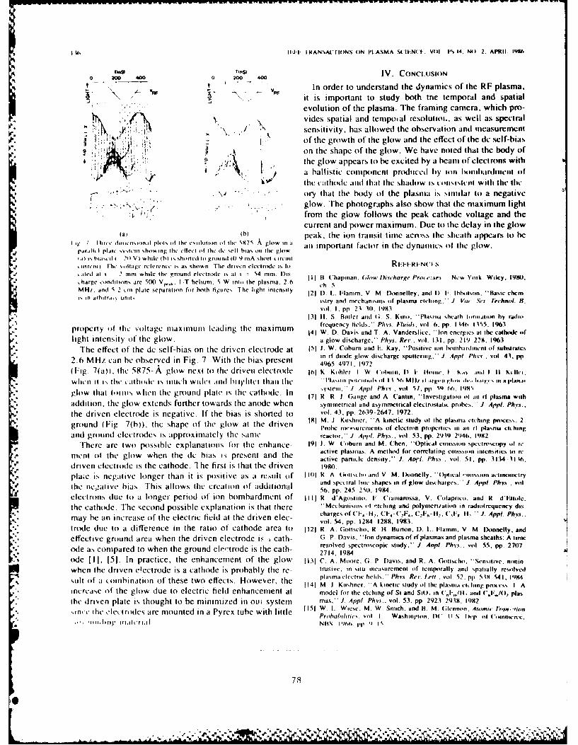
44,IA iI IIANSACrHONS ON PLASMVA 54Il1-N( §- Vol. Is, 14, MO 2. APIL 19116
200 0 IV. CONCL~USION
\AV W In order to understand the dynamics of the RF plasma.it is important to study both the temporal and spatialevolution of the plasma. The framing camera. which pro-
sensitivity, has allowed the observation andi mcasurrment
a - of the growth of the glow and the effect of the dc self-bias
3 on the shape of the glow. We have noted that the body of* 4)A the glow appears to be excited by a beam of electrons with' ~~~ aballii c comfpitincri nt Kt iced by io n b linha~irdine l of
V/ th tlcatiodc and that file shadow is coilsisltl walthlthe thc* v ~' -ory that the body of the plasma is similar to a negative
glow. The photograiphs also show. that the maximum light* front the glow follows the peak cathode voltage and the
current and power maximum. Due to the delay in the glow(b) peak, the ion transit time across the sheath appears to be
I ag I I hicc doiaacrasaon.al plans% taf the i'sohaaon of lace S97" gloaw il.1 ali important factor in the dynamiics of lte glow.para I II plat %cms slettasawi ng ic eia of the det %elf bias onl Ihe glow
* ~ajax hiasctl 2A) V) while Nh as shaarlcdta lgrnn( 419rmA shori-artmctarut wajlhc voa lta ge rc Ic rent cis as showni The driven ccl rode is Io RIIi:R IN(' N
,,alcd at 1 2 mmn whale the grounad electriode as at xa 54 mm. ias IlBChpaGoDicrgPote_.%NwYkWly,11.charge caaraaitions arc 5 00 V k I -T heaun. 5 W anto the plasmia. 2.6 ch. 5.MHt. and S 2 tin plate separation fair both figures. The light intensity 121 D, L. Flanmm. V M. florneliy. and 1) F Ihhaison, ''Basi chcmas in arbitrai units astry andt mechanismns aaf plasma eccling.' J Voat Sa, 1;ehnal- R.
van. 1. pp 23 304. 1983
131 It . S. Battler aaai G S. K ina. **Plasaria sheath lo ramitiam by radiao
property of lite voltage niaximulo leading the mnaximum frequency fields, P/aix. fluid.%, voal. 6. pp. 1 14t, I AW5 1963141 W. D. Davis and T A. Vanderslice. "Ion energies at the cathode oaf
light intensity of the glow, a glow discharge," Ph-vs. Rev.. vaol. 13 1. pp. 2 19 228. 1963.
*The effect of the dc self-bias on the driven electrode at 151 1. W. Coburn and E. Kay. "Positive ion hoarmtent aaf subs rate%* 7in rf daode glow dischargc sputtering:' J. Appl Phvai. vol 41, pp
2.6 MHz can be observed in Fig. 7.With the bias present 4965 4971. 1972
(Fig 7(a)., the 5875- A glow next to the drivenl electrodle 161 K Koahlat I W ('aiiari 1) 1-I' lagasa I ltas ,ad 1 11 Kalila'
* ~~when-I It I% lila- ;Illtaa c Is. Illtich wtlt l l 1 hI iI'fltel thiaiitel'lai Ia.'aaat alt I I Sri Mlt, a) aa1yan dv' I', laratas a ll a lan...r
* ~~glow tiat Ia ais .-.[flt lte ground plate Is the cathode. lIn t ylal J Ajapl P/ten , vol 57. ppi S4 66. I'INS171. R J Gatage and A. ('antin. ''Invstga ion of an rl plasma wath
*addition, the glow extends further towards the anode when symmetrical and asymrmetricat eletrostatic probes,' J Appi. PhY.;..
*the driven electrode is negative. If the bias is shorted to vol. 43. pp. 2639-2647. 1972.gon (Fg7(h) h shape oftego tthe driven 181 M. 3. Kiushner, 'A kinetic study of the plasma etching process 2
(Fig h' te'lw atPobe iaae-Nurenins aof clectron priaperes in an if plasma cithlngand ground electrodes is, approximately the sante. reaclaar." J Appa/. PhY., vad. 53, pp. 2919 2946, 19142
There are two possible explanations for thie enhance 191 J W Coburn and M. ('hen. ''Optical eanissljan spcctn"seaipy iat re
ment ot the glow when the dc bias is present and the active plasmtas: A methodl for correlatang cimlssian intensities to ractive partacle density.'* J. Apti. Plays . vial 51. pp. 3134-3116.
driven elecitrode is the cathode. 1 he first is that the driven 1980
plaic is negative longer than it is positive ats a restilt oaf lint1 R A Gcillt lit) anti V M. Doannelly, '' ooal iossan aclinilctry
the nc, aliye bias. This allows the creatiotn of' additional and spectral ]tiaa, shapes in r( glow discharges. 'J, Apid Phat , vol56. pp. 245 2sill. 1984.
electrons due to a longer period ofi ion bombardment of ill11 R dl'Agaslina. F ('tatalarossa, V. Caalaprtaa. and R4 d'Hlrl.
the cathode. The second possible explanation is that there "Mechanasnas (A "cthing and polymer/ioa~n in radarafrequenicy dis
may he an increase of the electric field at the driven dlee- chre fCF- CICF.CF-. 4',t .Ap.Py.
( rode due to a difference in the ratio of cathode area to 1121 R. A. Gottscho, R H. Burton, D. L. Flamm. V. M. tDonnelly, and
*effective ground area when the driven electrode is -i cath- G P. Davis. "Ion dynamics of rf plasmas and plasma sheaths: A time
* ode as, compared to when the ground electrode is the cath- resolved spectroscopic study," J. Api. Plays.. vol 55. pp. 27017I ~ de2714, 1984
od I 1, 151. In practice, the enhancement of the glow 113 1 C, A. Morore. G. P D~avis, anti R. A Gotischa. "Sensitive. oi
when the driven et ectrode is a cathode is probably tile re- truiavv. in %alu measuirement oaf temporally andi spatially resolvedt
stil afa cobintionof hesetwoeffets.Howeerthe 141plasma elect rac belds.'' Phvs Rev tn . vaal 5?. pip Si 4 541. 19M8. % illof t cmbiatio ofthee to efect. Hwevr, he 141M J Kaashncr. 'A kinetic siudy art tile plasmia cia ling prakess I A
* increase of the glow due to electric field enhancement at model faar the etching of Si and SaEJ, in C(1 1,,l and ('.F_,/ plas
the drtven plate is, thought to be minimized in out system may." J. Alpi. Plays.. vol. 53. pp 2923 2938. 1982,* srtia ic ~cctraalcsaremoutedin Pyex ubewit litle 11-51 W. IL. wiese. M. W. Smith. and Ii, M, (;icnnan. Atomic irin"aian
intth cl~iods re oute i a yrx ub wih itle Prhailiia, vaji I wash anlian .) 114 Its I lap iii ( ainnh'n'e
78
0%
- ~ ~ ~ ~ ~ ~ ~ ~ ~ ~ ~ e . .. X/%l ~ ~ ~ 4 * ~ ~ 7 ia.P

SECTION V
I
ENHANCEMENT OF THE PLASMA DENSITY AND DEPOSITION RATEIN RF DISCHARGES
-'S by5.
L. J. OverzetJ. T. Verdeyen
9.
['"4
-'4
4'
~79

Enhancement of the plasma density and deposition rate in rf dischargesL. J. Overzet and J. T. VerdeyenDepartment of Electrical and Computer Engineering, Uniwersity of Illinois at Urbana-Champaign, 1406 WestGreen Street. Urbana. Illinois 61801
(Received 6 December 1985; accepted for publication 20 January 1986)
The peak and time averaged electron density in rf excited silane-helium mixtures increasedsignificantly above the cw value by square wave modulating the source. The deposition rate ofamorphous hydrogenated silicon films is also enhanced and apparently follows the electrondensity. Attachment to the discharge products appears to be rsponsible.
Fhe properties of rfglow discharges in silane and heli- a 0.5% silane mixture in response to a SQWM excitation
um, as well as the materials deposited from these discharges, ( 100% modulation depth and 50% duty cycle) is comparedhave been the focus of extensive research.'' " One of the in Fig. 2 to that of a cw discharge at the same peak powermajor Impetus for research on the deposition kinetics of (and consequently twice the average power). The results foramorphous hydrogenated silicon has been the desire to pro- a helium discharge, shown in Fig. 2(a), follow intuitive log-duce high quality films at enhanced deposition rates. We ic. The square wave modulated source produces an essential-have uncovered a process which enhances deposition in low 1) square wave modulated electron density, and the identicalpower rf discharge% significantly. Both the deposition rate peak power to the discharge produces the same peak electronand the time averaged electron density have been enhanced density. Obviously, the decreased average power to theby square wave amplitude modulating (SQWM) the excita- SQWM glow produces a corresponding decrease (by a fac-tion of the silane-helium mixture (i.e.. 100% modulation tor of 2) in the time averaged electron density.depth and 50% duty cycle). Even though this work has con- The electron density in a 0.5% silane mixture does notcerned deposition, the data suggest that this phenomenon follow this intuitive logic as is illustrated in Fig. 2(b). Themay be found in other attaching gases including those used time dependence of the electron density in the SQWM glowfor etching. is no longer nearly square wave in shape, and despite having
The experimental apparatus in Fig. I is conventional in the same peak power, the instantaneous electron density isits essential features excepting perhaps our use of 2.9 rather radically different from the cw value. Indeed, Fig. 2(b)than 13.56 MHz. Power is coupled capacitively to the glow shows that the electron density has a rather complex andthrough the matching network shown in the upper section contorted time behavior, and has not reached the cw equilib-and the incident/reflected values are measured with a Birdwattmeter. An MKS 254A flow controller determines andIm onto . llt ow otgas thiough the plasina volune and alsocontrols the fractional silane content of the total. Typical 4 t "'lflows are in the range of 30 sccm for pressures on the order of (-L 2
0.6 Torr of 0-5% Si", in helium. 1. nol -T RE SOURC
A tuble pass microwave bridge circuit, shown below (2 , MazR
the discharge section it Fig. I. is u cd ito imeasure the elec- [ . Ltron density within the 4 cm diameter ( 5 cm discharge vol-ume. The microwave circuit involves a standard measure- REFLECTOR
ment technique which has been discussed extensively in the ___
literature. " Only the general idea is stressed here; namely, 9
the change in the detector output is directly proportional to ::___
the electron density. Electron densities greater than 107cm ' were measurable using this circuit at a microwave 7 L__frequency of 8.558 GHz. 5
The electron density is emphasized because of its micro- PROBE
scopic nature within the glow discharge and because it yields 2 I, 3information on a time scale which is short compared to most 3
kinetic reactions. By way of comparison, the macroscopic MICROWAVE SOURCEgrowth rate or film quality are integrations over large timeperiods of complex and often competing processes. Despite[ DISPI ,vthis difference in the nature of these observables, we have 7 -found that the deposition rate follows the dependence of the Rf FERIqL F ARM
time averaged electron density, in agreement with Turban 2 'and Kampa ,,." FIG I rf matching network (tipper), plasma region (center), and micro-
The time evolution ofI lie eiect ron den,,i , in helium and wa ,t hridg e cirtt111 (lower)
6015 Ap)p Phy, oIll 48 1 1) / \lMdr, t, 981 h 000A-6951/86' 10695-03$01 00 1986 Am orcan InStIte Of PhySICS 695
4 80-,-,

T I T - _ ' I T o_ _T
00: z
-n - - --- - - : -j - Growln
' wv 2500
00
'J I 200. ..
ziw
> o5 CW Fleciron Oestv
LAJ
,, 0 1000 10.000
------ -- -- MODULATION FREOUENCY (H)
FIG. 4. Total film thickness after 15 min and time averaged electron densityduring the growth as a function of the modulation frequency. The peak
FIG. 2 Time dependence ofthe electron density for a square wave modulat- power varied between the data points, but remained in the 15-o8Wrange.
ed ecittio sorce(SQW ) (100/c oduatio deth nd 0% uty All diacharges were I% silane in helium at approximately 0.6 Torr.*,'ed escitation source (SQWM) (100%/ modulation depth and 50%o duty
cycle) and a continuous wave source (cw) in (a) helium and (b) 0.5%silane in helium, with the time averaged electron density during the growth.
These films were grown on quartz substrates placed on the
rium value even in the 50 ms on time. Consequently, the driven electrode (in Fig. I ) and the film thickness was mea-
density averaged over the period of modulation is consider- sured with a Dektak profiiometer. Note that the data points
ably larger for the SQWM excitation as can be deduced from shown in Fig. 4 were not all taken at the same peak powerFiger b. tand thus the densities shown in Figs. 3 and 4 cannot be com-* - Fig. 2(b).
The dependence of the electron density on the modula- pared: however, the correlation between electron densityThe epedene o th elctro desit onthemodla- and deposition in Fig. 4 is significant. The deposition ratetion frequency is shown in Fig. 3. For a constant peak power an bepsen e to f th agnitudeot ele
of 18 W, the time averaged electron density can be enhanced can be seen there to follow the magnitude of the electron
by as much as a factor of 2-3 in the SQWM glow. For low density.
( < 5 Hz) and for high ( > 5 kHz) modulation frequencies, Both the contorted time evolution shown in Fig. 2 and
the time averaged electron density in the SQWM glow ap- the enhancement of the time averaged electron density in
proaches the expected 1/2 of the cw value. The film thick- Fig. 3 indicate a complex interrelationship between the elec-
ness (for a 15-min deposition time) is shown in Fig. 4 along tron density, ion density, and the depositing species. Whilethe exact electron-ion kinetics are not clear from the datapresented in Figs. 2 and 3, one may speculate based uponthese data. In Fig. 2(b), the electron density increases to ahigh value initially and then decreases to a quasi-equilibriumvalue. This time dependence is consistent with the results ofFleddermann et al.4 who demonstrated that the products ofsilane dissociation attached electrons faster than silane itself.These products are not within the discharge when it is firstturned on; therefore the electron density rises quickly. Asthe discharge proceeds, however, silane is dissociated into
'4'these attaching products, and attachment produces the rap-id decay of the electron density after its initial rise. Unfortu-
nately, the secondary increase of electron density [in Fig., 2 (b) ]land the approach to the cw value are not understood at
this time.
The fact that the deposition rate increases in the SQWMdischarge even though the time averaged power is halvedmay indicate that the products-possibly even the negative
00I,,t A ,nN F RI QUF N( ' ions-of the initial silane dissociation are involved in deposi-tion. These negative ions are confined by the sheaths in the
FIG. 3. Dependence of the time averaged electron density on the square
wave modulation frequency in a I% silane discharge (0 6Torr) The peak same manner as are electrons in the cw glow. Hence thepower I. -- i W. enhanced growth rate iti the SQWM glow may be partially
696 Appi Phys Lett., Vol 48, No 11. 17 March 1986 L J Overzet ano J T Vvideyon 696
81

* due to deposition by the negatively charged radicals in the 'G Turban. Y Cathenne and G. Grolleau. Thin Solid Films 60. 147
afterglow when such sheaths are greatly reduced. This spec- (1979)'G Turban. Y. Catherine. and G. Grolleau. Plasma Chent. Plasma Pro-ulation regarding the enhancement remains to be proven. cc- h. a1 (19e2.
Even though the detailed processes are not known at the 'C B Fleddermann, J H. Beherman, and J T Verdeyen. J AppI Phys. 5I,
present time, it is surely true that the enhanced electron den- 1 344 (1985)
sily in the SQWM glow permits an increase in the neutral 'It I Sterling and R C Gi Swann. Solid Stale Fletkroii 8. 654 ( 1)65)'W L. Spear and P G I ecmnihicr, stlili State ('oniunun 17. 11)) I ( 1975)
and ionic products along with an enhanced deposition rate. 'B A Scott, M It. Ilradsky. I) C Green. I' B Kirby. R M I'lecenik, and
p' * Similar effects may be found in etching discharges; indeed, E. E Simonyi. AppI. Phys. Let 37. 725 (1980)
there maybea hint of this in a recent paper." The authors 'F.J KampasandR. W. Griffith, Appl. Phys Len 39,407 (1981)
have also observed a similar (although somewhat less pro- 'F. J Kampas. J Appi Phys 54. 2276 (1983).'J. C Knight,. Jpn J Appi Phys. Suppi IS-i. 101 (1979)nounced) enhancement in the electron density in a CF, "R A Street. J C" Knight., and D K. Biegelen. Phys Rev. B II, 180
glow. (1980)
This work was supported by the U.S. Air Force Aero- 'A Garscadden, G t.. Duke, and W F Bailey, Appl. Phys. Lett. 43, 1012nautical Systems Division (AFSC) Wright-Patterson Air ,(83).Gillardini. LowEneryElectronColhsionsiGases, st d. (Wiley,
'AL.Gllrin.LForce Bacse.oliinsinGse.lv d.(ilyForce Base. New York. 1972), pp. 236-254
"A, K. Bhattacharya. J T Verdeyen. F T Adler. and L Goldstein, J_'J C Knight, R A ILujan, M P Roenhlmini. R A Street. D. K. Biegel- AppI. Phys 38, 527 (1967)'.en. and .I A Reimer. AppI. Phys, .eit 38. .1 ( 1481) "R W. Roswell and D Henry. AppI Phy% Lett 47, 1095 (1985).
Sm
S.
697 APPI Phys Leftt, Vol 48 No 11 1 7 March 1986 L J Overzet and J T Verdeyen 697
P 82

Lr-/
c INIMM66
Related Documents