UM10391 90 Watt notebook adapter with TEA1751T and TEA1791T Rev. 01 — 20 April 2010 User manual Document information Info Content Keywords GreenChip III, TEA1751T, GreenChip SR, TEA1791T, PFC, flyback, synchronous rectification, high efficiency, adapter, notebook, PC power Abstract This manual provides the specification, performance, schematics, bill of materials and PCB layout of a 90 W notebook adapter with the TEA1751T and TEA1791T. For design details on the TEA1751T and TEA1791T please refer to the application notes.

Welcome message from author
This document is posted to help you gain knowledge. Please leave a comment to let me know what you think about it! Share it to your friends and learn new things together.
Transcript
UM1039190 Watt notebook adapter with TEA1751T and TEA1791TRev. 01 — 20 April 2010 User manual
Document informationInfo ContentKeywords GreenChip III, TEA1751T, GreenChip SR, TEA1791T, PFC, flyback,
synchronous rectification, high efficiency, adapter, notebook, PC power
Abstract This manual provides the specification, performance, schematics, bill of materials and PCB layout of a 90 W notebook adapter with the TEA1751T and TEA1791T. For design details on the TEA1751T and TEA1791T please refer to the application notes.
NXP Semiconductors UM1039190 Watt notebook adapter with TEA1751T and TEA1791T
Revision history Rev Date Description
UM10391_1 20100420 First release
UM10391_1 All information provided in this document is subject to legal disclaimers. © NXP B.V. 2010. All rights reserved.
User manual Rev. 01 — 20 April 2010 2 of 37
Contact informationFor more information, please visit: http://www.nxp.com
For sales office addresses, please send an email to: [email protected]

NXP Semiconductors UM1039190 Watt notebook adapter with TEA1751T and TEA1791T
1. Introduction
This manual describes a universal input, 19.5 V, 4.62 A single output power supply using TEA1751T and TEA1791T devices from NXPsemiconductor’s GreenChip III and GreenChip-SR family. It contains the power supply specifications, circuit diagram, component list to build the supply, PCB layout and component positions, PFC choke and transformer documentation, along with test data and oscilloscope pictures of the most important waveforms.
The GreenChip III combines the control and drive functions for both the PFC and the flyback stages into a single device. The TEA1751T provides complete SMPS control functionality to comply with the IEC61000-3-2 harmonic current emission requirements, obtain a significant reduction of components, save PCB space and give a cost benefit. It also offers extremely low power consumption in no-load mode, which makes it suitable for the low-power consumer markets. The special built-in green functions allow a high efficiency at all power levels which results in a design that can easily meet all existing and proposed energy efficiency standards such as Code of Conduct (Europe), Energy Star (US), California Energy Commission, Minimum Energy Performance Standards (Australian & New Zealand) and China Energy Conservation Program.
The GreenChip SR is the only synchronous rectification control IC available that needs no external components for tuning of the timing. Used in notebook adapter designs, the GreenChip SR offers a wide VCC operation range of 8.5 V to 38 V, minimizing the number of external components required and enabling simpler designs. In addition, the high driver output voltage (10 V) makes the GreenChip SR compatible with all brands of MOSfets.
Fig 1. 90 W TEA1751T and TEA1791T demo board
001aak826
UM10391_1 All information provided in this document is subject to legal disclaimers. © NXP B.V. 2010. All rights reserved.
User manual Rev. 01 — 20 April 2010 3 of 37
NXP Semiconductors UM1039190 Watt notebook adapter with TEA1751T and TEA1791T
2. Specification
• Mains input voltage: 90 V to 264 V, 47 Hz to 63 Hz• DC output: 19.5 V, 2 %• Maximum continuous output current: 4.62 A• Peak output current: 7.5 A• Efficiency: > 87 % at maximum load• CEC active mode efficiency: > 90 % • No load power consumption: < 0.3 W• Dynamic load response: < +1 V / −0.5 V• Output ripple and noise: 100 mVp-p(max.)
• CISPR22 class B conducted EMI• EN61000-4-2 immunity against ESD• EN61000-3-2 A14 (harmonics) compliance• Short Circuit Protection (SCP) and output Over-Current Protection (OCP);
input power < 3 W at both SCP and OCP test• Latched output Over Voltage Protection (OVP): < 25 V• Latched Over Temperature Protection (OTP)• Fast Latch Reset (FLR): < 3 sec.
3. Performance data
3.1 Test setup
3.1.1 Test equipment
• Programmable AC Source: Chroma, Model 61503• Power HiTester: Hioki, Model 3332• DC Electronic Load: Chroma, Model 63030• Digital Oscilloscope: Tektronix, Model TDS5104B• Current Probe/Amplifier: Tektronix, Model TCP305/TCPA300• 100 MHz, High Voltage Differential Probe: Tektronix, Model P5205• 6-Digit Multimeter: Agilent, Model 34401A• EMC receiver Rohde & Schwarz ESPI-3 + LISN ENV216
3.1.2 Test conditions
• Unit on the lab-table with the heat sinks downwards• No casing was present on the unit• Lab temperature between 20 °C and 25 °C• Measurements were made after stabilization of temperature according “test method
for calculating the efficiency of single-voltage external AC-DC and AC-AC power supplies” of Energy Star
UM10391_1 All information provided in this document is subject to legal disclaimers. © NXP B.V. 2010. All rights reserved.
User manual Rev. 01 — 20 April 2010 4 of 37
NXP Semiconductors UM1039190 Watt notebook adapter with TEA1751T and TEA1791T
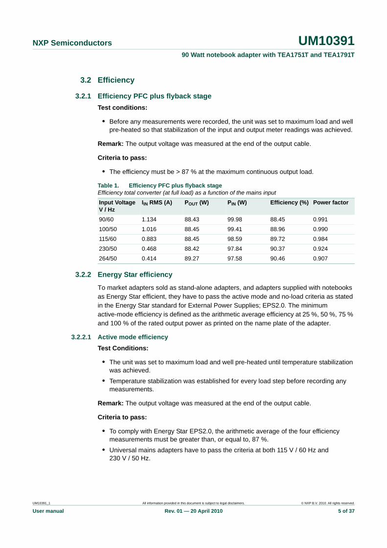
3.2 Efficiency
3.2.1 Efficiency PFC plus flyback stageTest conditions:
• Before any measurements were recorded, the unit was set to maximum load and well pre-heated so that stabilization of the input and output meter readings was achieved.
Remark: The output voltage was measured at the end of the output cable.
Criteria to pass:
• The efficiency must be > 87 % at the maximum continuous output load.
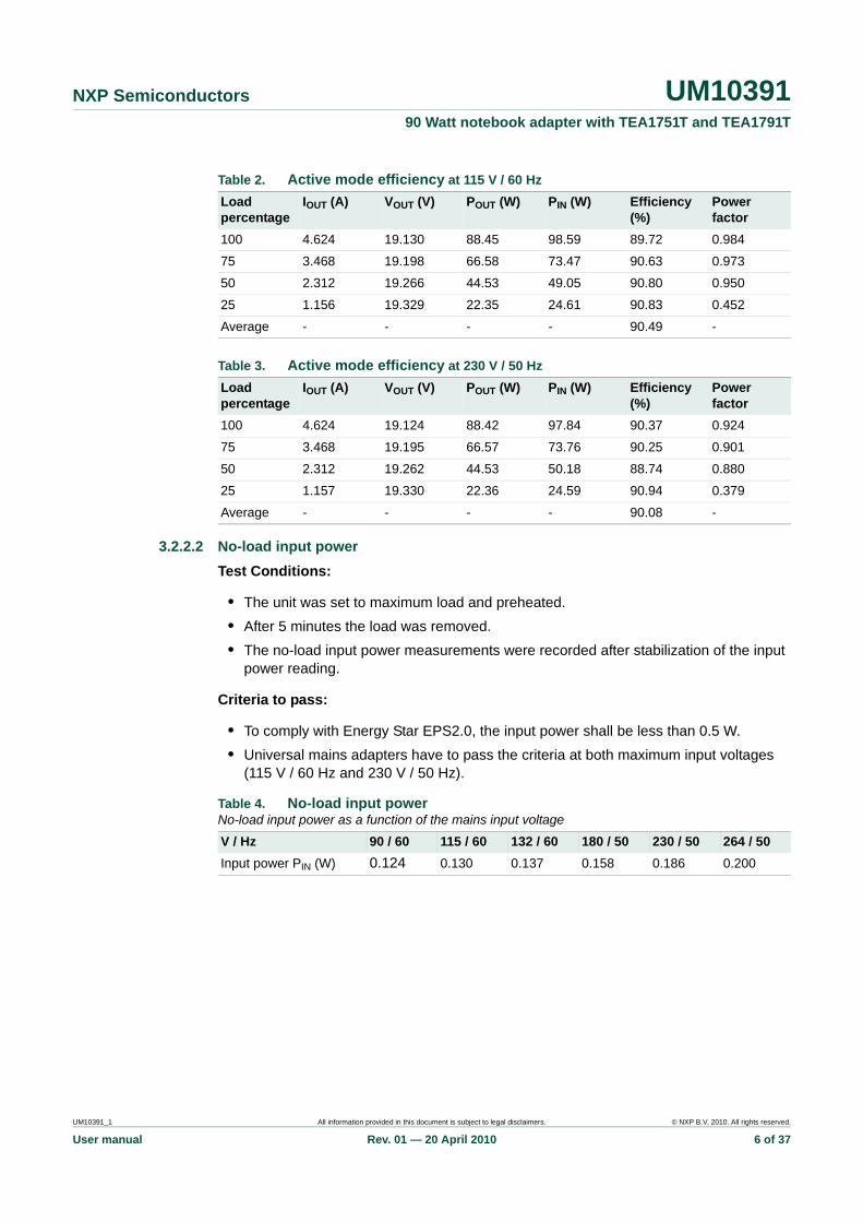
3.2.2 Energy Star efficiency
To market adapters sold as stand-alone adapters, and adapters supplied with notebooks as Energy Star efficient, they have to pass the active mode and no-load criteria as stated in the Energy Star standard for External Power Supplies; EPS2.0. The minimum active-mode efficiency is defined as the arithmetic average efficiency at 25 %, 50 %, 75 % and 100 % of the rated output power as printed on the name plate of the adapter.
3.2.2.1 Active mode efficiencyTest Conditions:
• The unit was set to maximum load and well pre-heated until temperature stabilization was achieved.
• Temperature stabilization was established for every load step before recording any measurements.
Remark: The output voltage was measured at the end of the output cable.
Criteria to pass:
• To comply with Energy Star EPS2.0, the arithmetic average of the four efficiency measurements must be greater than, or equal to, 87 %.
• Universal mains adapters have to pass the criteria at both 115 V / 60 Hz and 230 V / 50 Hz.
Table 1. Efficiency PFC plus flyback stage Efficiency total converter (at full load) as a function of the mains input
Input Voltage V / Hz
IIN RMS (A) POUT (W) PIN (W) Efficiency (%) Power factor
90/60 1.134 88.43 99.98 88.45 0.991
100/50 1.016 88.45 99.41 88.96 0.990
115/60 0.883 88.45 98.59 89.72 0.984
230/50 0.468 88.42 97.84 90.37 0.924
264/50 0.414 89.27 97.58 90.46 0.907
UM10391_1 All information provided in this document is subject to legal disclaimers. © NXP B.V. 2010. All rights reserved.
User manual Rev. 01 — 20 April 2010 5 of 37
NXP Semiconductors UM1039190 Watt notebook adapter with TEA1751T and TEA1791T
3.2.2.2 No-load input powerTest Conditions:
• The unit was set to maximum load and preheated.• After 5 minutes the load was removed.• The no-load input power measurements were recorded after stabilization of the input
power reading.
Criteria to pass:
• To comply with Energy Star EPS2.0, the input power shall be less than 0.5 W.• Universal mains adapters have to pass the criteria at both maximum input voltages
(115 V / 60 Hz and 230 V / 50 Hz).
Table 2. Active mode efficiency at 115 V / 60 Hz Load percentage
IOUT (A) VOUT (V) POUT (W) PIN (W) Efficiency (%)
Power factor
100 4.624 19.130 88.45 98.59 89.72 0.984
75 3.468 19.198 66.58 73.47 90.63 0.973
50 2.312 19.266 44.53 49.05 90.80 0.950
25 1.156 19.329 22.35 24.61 90.83 0.452
Average - - - - 90.49 -
Table 3. Active mode efficiency at 230 V / 50 Hz Load percentage
IOUT (A) VOUT (V) POUT (W) PIN (W) Efficiency (%)
Power factor
100 4.624 19.124 88.42 97.84 90.37 0.924
75 3.468 19.195 66.57 73.76 90.25 0.901
50 2.312 19.262 44.53 50.18 88.74 0.880
25 1.157 19.330 22.36 24.59 90.94 0.379
Average - - - - 90.08 -
Table 4. No-load input power No-load input power as a function of the mains input voltage
V / Hz 90 / 60 115 / 60 132 / 60 180 / 50 230 / 50 264 / 50Input power PIN (W) 0.124 0.130 0.137 0.158 0.186 0.200
UM10391_1 All information provided in this document is subject to legal disclaimers. © NXP B.V. 2010. All rights reserved.
User manual Rev. 01 — 20 April 2010 6 of 37
NXP Semiconductors UM1039190 Watt notebook adapter with TEA1751T and TEA1791T
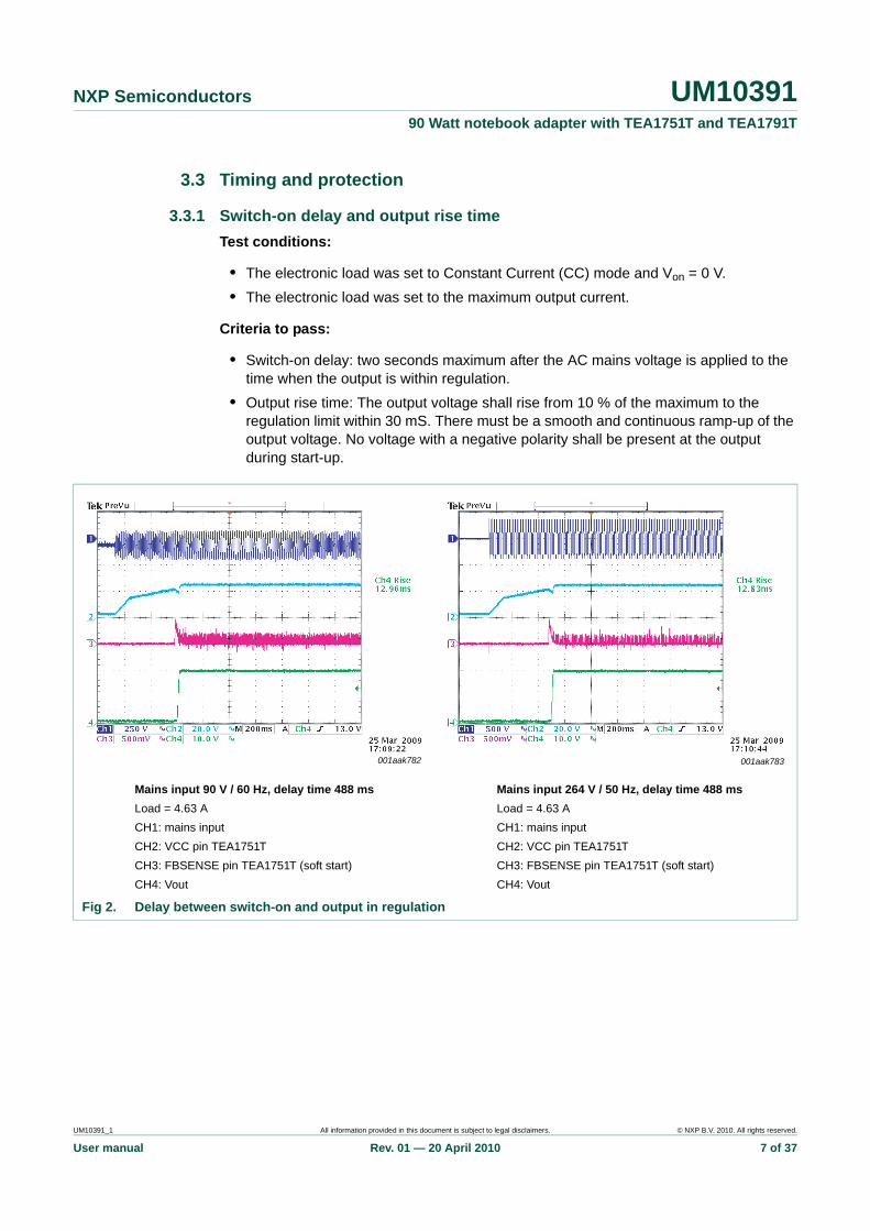
3.3 Timing and protection
3.3.1 Switch-on delay and output rise timeTest conditions:
• The electronic load was set to Constant Current (CC) mode and Von = 0 V.• The electronic load was set to the maximum output current.
Criteria to pass:
• Switch-on delay: two seconds maximum after the AC mains voltage is applied to the time when the output is within regulation.
• Output rise time: The output voltage shall rise from 10 % of the maximum to the regulation limit within 30 mS. There must be a smooth and continuous ramp-up of the output voltage. No voltage with a negative polarity shall be present at the output during start-up.
Mains input 90 V / 60 Hz, delay time 488 msLoad = 4.63 ACH1: mains inputCH2: VCC pin TEA1751TCH3: FBSENSE pin TEA1751T (soft start)CH4: Vout
Mains input 264 V / 50 Hz, delay time 488 msLoad = 4.63 ACH1: mains inputCH2: VCC pin TEA1751TCH3: FBSENSE pin TEA1751T (soft start)CH4: Vout
Fig 2. Delay between switch-on and output in regulation
001aak782 001aak783
UM10391_1 All information provided in this document is subject to legal disclaimers. © NXP B.V. 2010. All rights reserved.
User manual Rev. 01 — 20 April 2010 7 of 37
NXP Semiconductors UM1039190 Watt notebook adapter with TEA1751T and TEA1791T
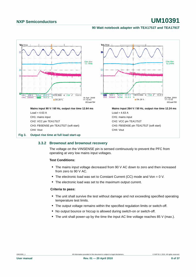
3.3.2 Brownout and brownout recoveryThe voltage on the VINSENSE pin is sensed continuously to prevent the PFC from operating at very low mains input voltages.
Test Conditions:
• The mains input voltage decreased from 90 V AC down to zero and then increased from zero to 90 V AC.
• The electronic load was set to Constant Current (CC) mode and Von = 0 V.• The electronic load was set to the maximum output current.
Criteria to pass:
• The unit shall survive the test without damage and not exceeding specified operating temperature test limits.
• The output voltage remains within the specified regulation limits or switch-off.• No output bounce or hiccup is allowed during switch-on or switch-off.• The unit shall power-up by the time the input AC line voltage reaches 85 V (max.).
Mains input 90 V / 60 Hz, output rise time 12.64 msLoad = 4.63 ACH1: mains inputCH2: VCC pin TEA1751TCH3: FBSENSE pin TEA1751T (soft start)CH4: Vout
Mains input 264 V / 50 Hz, output rise time 12.24 msLoad = 4.63 ACH1: mains inputCH2: VCC pin TEA1751TCH3: FBSENSE pin TEA1751T (soft start)CH4: Vout
Fig 3. Output rise time at full load start-up
001aak784 001aak785
UM10391_1 All information provided in this document is subject to legal disclaimers. © NXP B.V. 2010. All rights reserved.
User manual Rev. 01 — 20 April 2010 8 of 37

NXP Semiconductors UM1039190 Watt notebook adapter with TEA1751T and TEA1791T
3.3.3 Output short circuit and open loop protection
To protect the adapter and application against an output short circuit or a single fault open (flyback) feedback loop situation, a time-out protection is implemented. When the voltage on FBCTRL pin rises above 4.5 V (typ.), a fault is assumed and switching is blocked.
The time-out protection should not trigger during a normal start-up with maximum load.
3.3.3.1 Open loop protectionTest Conditions:
• The electronic load was set to Constant Current (CC) mode and Von = 0 V.• The electronic load is set to the maximum output current.
Criteria to pass:
• A normal start-up with a smooth and continuous ramp-up of the output voltage.• No output bounce or hiccup is allowed during switch-on or switch-off.• There be must be sufficient margin between the FBCTRL level and the 4.5 V time-out
trigger level to avoid false triggering of the time-out protection due to component tolerances.
Mains input from 90 V AC to 0 V AC, brownout voltage 70 V ACLoad = 4.63 ACH1: mains inputCH2: Vdrn PFC MosfetCH3: Vdrn flyback MosfetCH4: Vout
Mains input from 0 V AC to 90 V AC, brownout recovery 75 V ACLoad = 4.63 ACH1: mains inputCH2: Vdrn PFC MosfetCH3: Vdrn flyback MosfetCH4: Vout
Fig 4. Brownout and brownout recovery
001aak787 001aak786
UM10391_1 All information provided in this document is subject to legal disclaimers. © NXP B.V. 2010. All rights reserved.
User manual Rev. 01 — 20 April 2010 9 of 37
NXP Semiconductors UM1039190 Watt notebook adapter with TEA1751T and TEA1791T
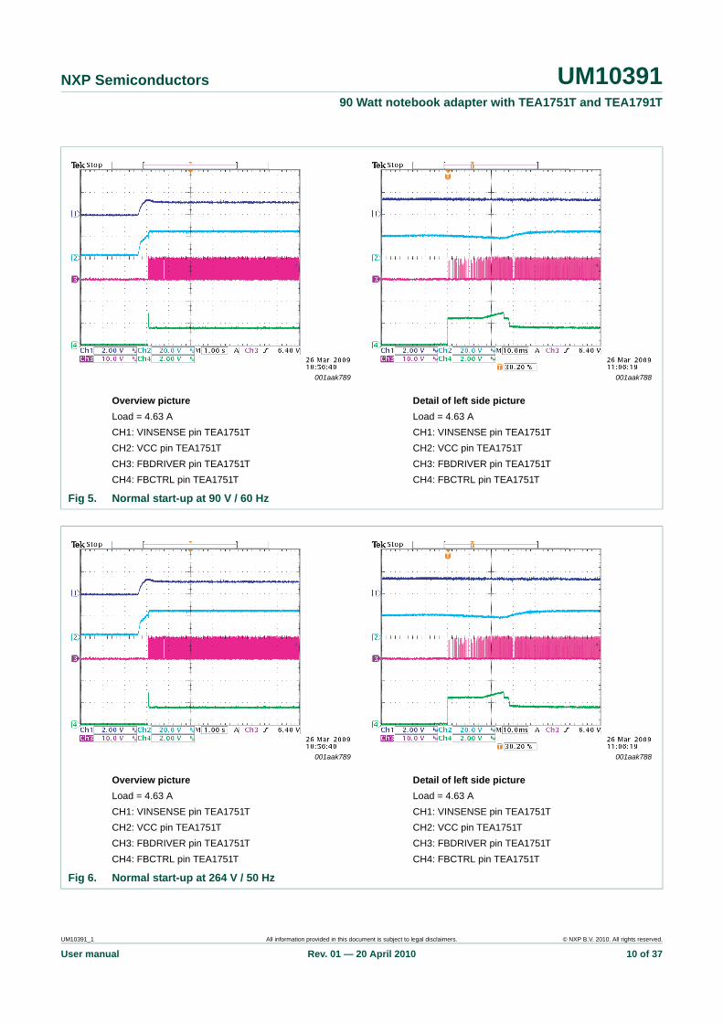
Overview pictureLoad = 4.63 ACH1: VINSENSE pin TEA1751TCH2: VCC pin TEA1751TCH3: FBDRIVER pin TEA1751TCH4: FBCTRL pin TEA1751T
Detail of left side pictureLoad = 4.63 ACH1: VINSENSE pin TEA1751TCH2: VCC pin TEA1751TCH3: FBDRIVER pin TEA1751TCH4: FBCTRL pin TEA1751T
Fig 5. Normal start-up at 90 V / 60 Hz
001aak789 001aak788
Overview pictureLoad = 4.63 ACH1: VINSENSE pin TEA1751TCH2: VCC pin TEA1751TCH3: FBDRIVER pin TEA1751TCH4: FBCTRL pin TEA1751T
Detail of left side pictureLoad = 4.63 ACH1: VINSENSE pin TEA1751TCH2: VCC pin TEA1751TCH3: FBDRIVER pin TEA1751TCH4: FBCTRL pin TEA1751T
Fig 6. Normal start-up at 264 V / 50 Hz
001aak789 001aak788
UM10391_1 All information provided in this document is subject to legal disclaimers. © NXP B.V. 2010. All rights reserved.
User manual Rev. 01 — 20 April 2010 10 of 37
NXP Semiconductors UM1039190 Watt notebook adapter with TEA1751T and TEA1791T
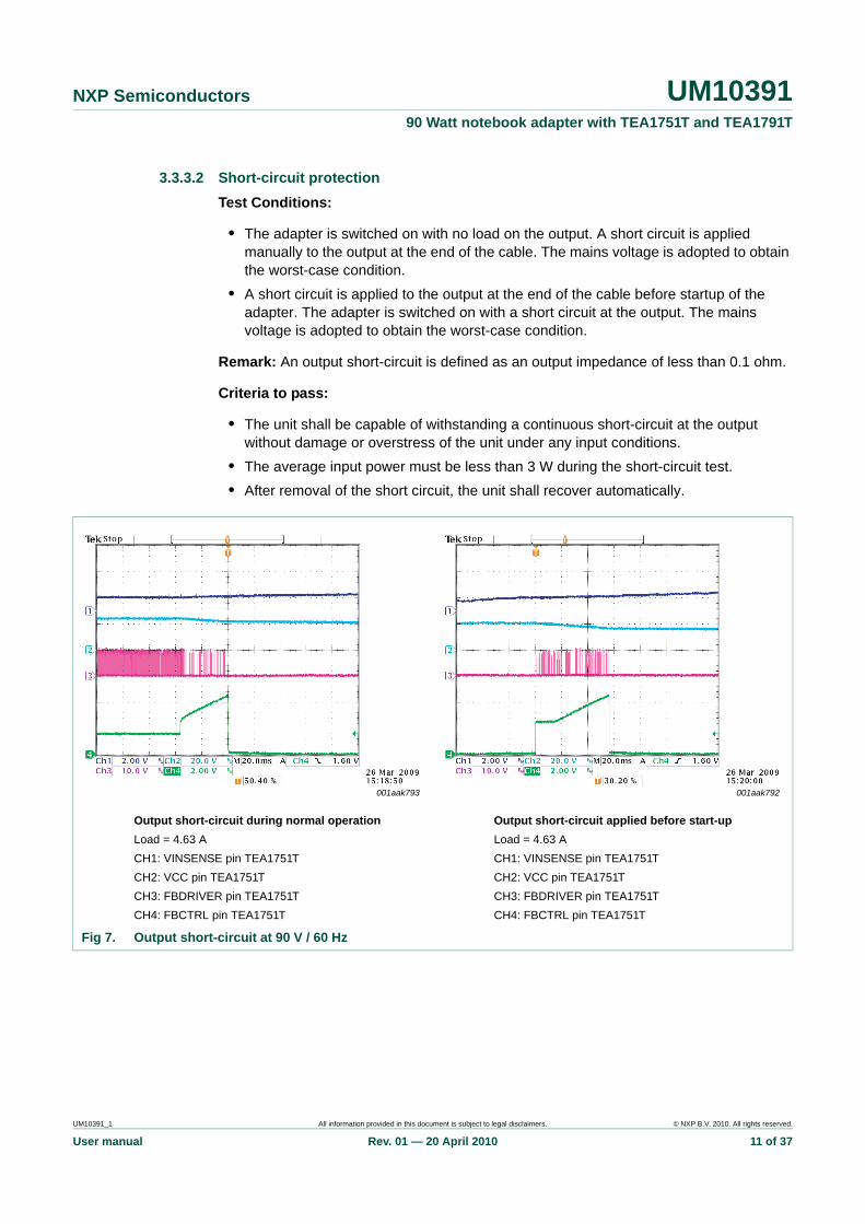
3.3.3.2 Short-circuit protectionTest Conditions:
• The adapter is switched on with no load on the output. A short circuit is applied manually to the output at the end of the cable. The mains voltage is adopted to obtain the worst-case condition.
• A short circuit is applied to the output at the end of the cable before startup of the adapter. The adapter is switched on with a short circuit at the output. The mains voltage is adopted to obtain the worst-case condition.
Remark: An output short-circuit is defined as an output impedance of less than 0.1 ohm.
Criteria to pass:
• The unit shall be capable of withstanding a continuous short-circuit at the output without damage or overstress of the unit under any input conditions.
• The average input power must be less than 3 W during the short-circuit test.• After removal of the short circuit, the unit shall recover automatically.
Output short-circuit during normal operationLoad = 4.63 ACH1: VINSENSE pin TEA1751TCH2: VCC pin TEA1751TCH3: FBDRIVER pin TEA1751TCH4: FBCTRL pin TEA1751T
Output short-circuit applied before start-upLoad = 4.63 ACH1: VINSENSE pin TEA1751TCH2: VCC pin TEA1751TCH3: FBDRIVER pin TEA1751TCH4: FBCTRL pin TEA1751T
Fig 7. Output short-circuit at 90 V / 60 Hz
001aak793 001aak792
UM10391_1 All information provided in this document is subject to legal disclaimers. © NXP B.V. 2010. All rights reserved.
User manual Rev. 01 — 20 April 2010 11 of 37

NXP Semiconductors UM1039190 Watt notebook adapter with TEA1751T and TEA1791T
Output short-circuit during normal operationLoad = 4.63 ACH1: VINSENSE pin TEA1751TCH2: VCC pin TEA1751TCH3: FBDRIVER pin TEA1751TCH4: FBCTRL pin TEA1751T
Output short-circuit applied before start-upLoad = 4.63 ACH1: VINSENSE pin TEA1751TCH2: VCC pin TEA1751TCH3: FBDRIVER pin TEA1751TCH4: FBCTRL pin TEA1751T
Fig 8. Output short-circuit at 264 V / 50 Hz
001aak795 001aak794
Mains input 90 V / 60 Hz; input power 0.96 WLoad = 0 ACH1: VCC pin TEA1751TCH2: FBCTRL pin TEA1751TCH3: Vdrn flyback MosfetCH4: Vout
Mains input 264 V / 50 Hz; input power 0.84 WLoad = 0 ACH1: VCC pin TEA1751TCH2: FBCTRL pin TEA1751TCH3: Vdrn flyback MosfetCH4: Vout
Fig 9. Output short-circuit protection
001aak796 001aak797
UM10391_1 All information provided in this document is subject to legal disclaimers. © NXP B.V. 2010. All rights reserved.
User manual Rev. 01 — 20 April 2010 12 of 37

NXP Semiconductors UM1039190 Watt notebook adapter with TEA1751T and TEA1791T
3.3.4 Over-current protectionTest Conditions:
• The load was increased from the maximum value to an estimated over-current value in several steps.
• The test was repeated for different input voltages.
Criteria to pass:
• The output power should be limited and may not exceed 240 W, just before the triggering of the over current protection.
• The average input power shall be less than 3 W once the over current protection has been triggered.
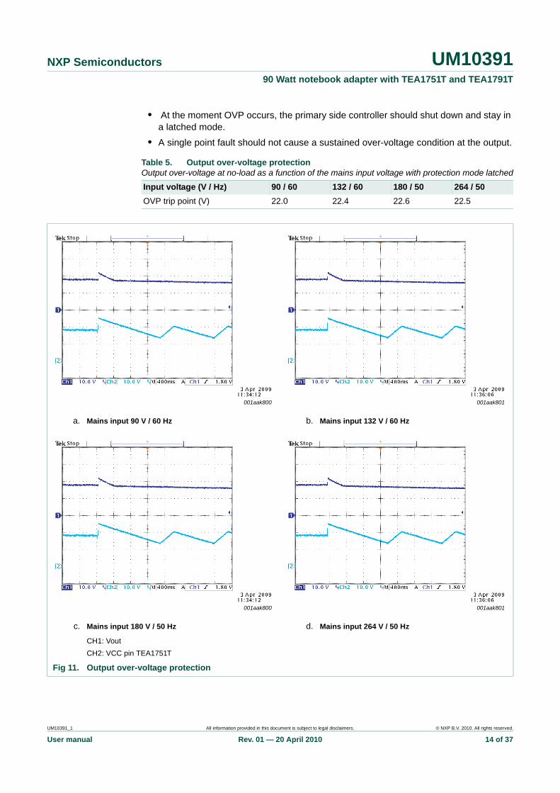
3.3.5 Output Over-Voltage Protection (OVP)Test Conditions:
• An output overvoltage was created by applying a short circuit across the opto LED of U2.
• An AC input voltage was selected so that the worst-case condition occurred.• There was no load on the output.
Criteria to pass:
• The output voltage may not exceed 25 V or stabilize between 25 V and the rated voltage.
Mains input 90 V / 60 Hz; Io_OCP 8.72 A; input power 1.26 WLoad before short-circuit = 0 ACH1: VCC pin TEA1751TCH2: FBCTRL pin TEA1751TCH3: Vdrn flyback MosfetCH4: Vout
Mains input 264 V / 50 Hz; Io_OCP 9.02 A; input power 1.14 WLoad before short-circuit = 0 ACH1: VCC pin TEA1751TCH2: FBCTRL pin TEA1751TCH3: Vdrn flyback MosfetCH4: Vout
Fig 10. Output over current protection
001aak798 001aak799
UM10391_1 All information provided in this document is subject to legal disclaimers. © NXP B.V. 2010. All rights reserved.
User manual Rev. 01 — 20 April 2010 13 of 37
NXP Semiconductors UM1039190 Watt notebook adapter with TEA1751T and TEA1791T
• At the moment OVP occurs, the primary side controller should shut down and stay in a latched mode.
• A single point fault should not cause a sustained over-voltage condition at the output.
Table 5. Output over-voltage protection Output over-voltage at no-load as a function of the mains input voltage with protection mode latched
Input voltage (V / Hz) 90 / 60 132 / 60 180 / 50 264 / 50OVP trip point (V) 22.0 22.4 22.6 22.5
a. Mains input 90 V / 60 Hz b. Mains input 132 V / 60 Hz
c. Mains input 180 V / 50 Hz d. Mains input 264 V / 50 Hz
CH1: VoutCH2: VCC pin TEA1751T
Fig 11. Output over-voltage protection
001aak800 001aak801
001aak800 001aak801
UM10391_1 All information provided in this document is subject to legal disclaimers. © NXP B.V. 2010. All rights reserved.
User manual Rev. 01 — 20 April 2010 14 of 37

NXP Semiconductors UM1039190 Watt notebook adapter with TEA1751T and TEA1791T
3.3.6 Over-temperature protection
An accurate external over temperature protection (TEA1751T LATCH pin, RT2, R26 and C19) is provided in the demo board to protect the flyback transformer against overheating. Normally, the flyback transformer is the most heat sensitive component.
Test Conditions:
• The NTC temperature sensor, glued to the transformer, was heated using a heat gun.
Criteria to pass:
• The IC should latch off the output at a VLATCH trip level of 1.25V. No output bounce or hiccup is allowed.
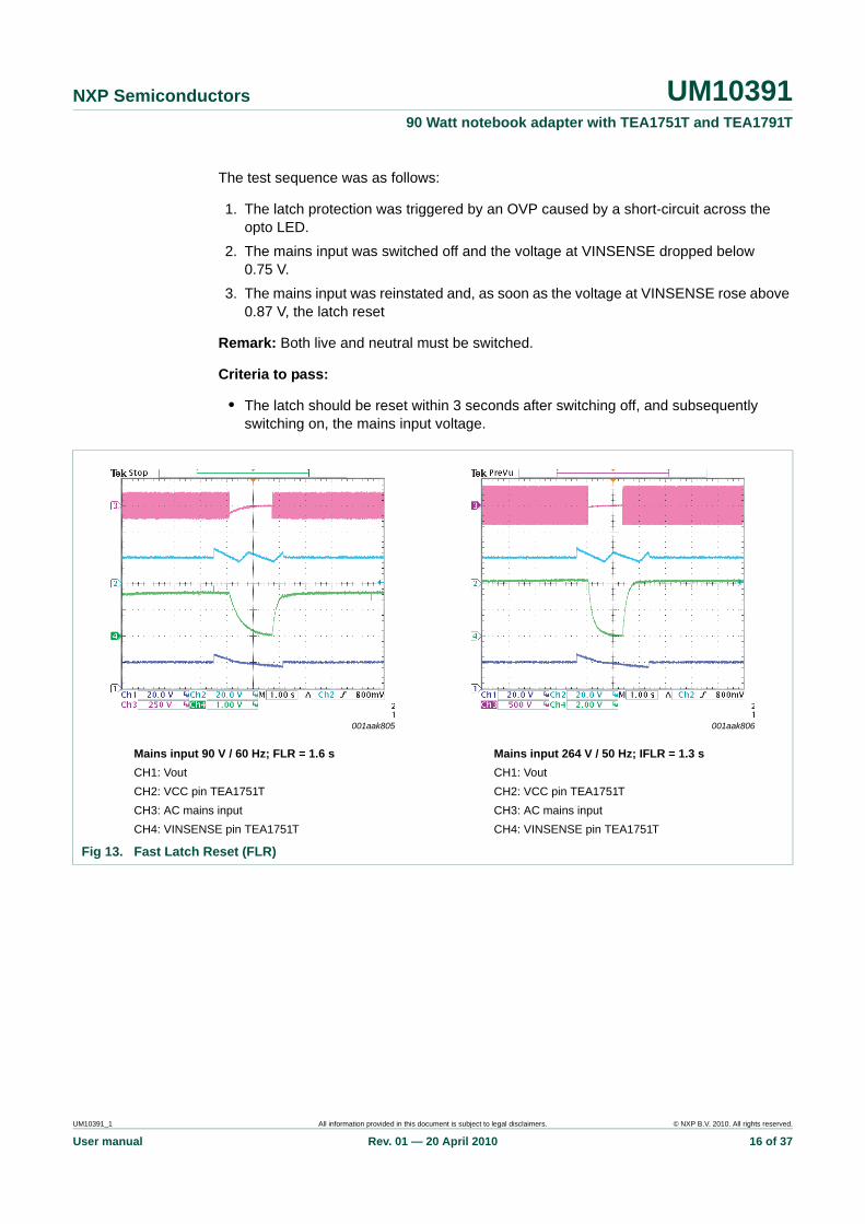
3.3.7 Fast latch resetA fast latch reset function (FLR) is implemented to enable latched protection to be reset without discharging the bulk electrolytic capacitor. The latch protection will be reset as soon as the voltage on VINSENSE pin drops below 0.75 V and then raised to 0.87 V.
Test conditions:
• No load at the output.
OTP trigger temperature 108 ×C Load before short-circuit = 0 ACH1: VoutCH2: TEA1751T VCC pin CH3: Mains input voltageCH4: TEA1751T LATCH pin
Fig 12. External Over Temperature Protection (OTP)
001aak804
UM10391_1 All information provided in this document is subject to legal disclaimers. © NXP B.V. 2010. All rights reserved.
User manual Rev. 01 — 20 April 2010 15 of 37
NXP Semiconductors UM1039190 Watt notebook adapter with TEA1751T and TEA1791T
The test sequence was as follows:
1. The latch protection was triggered by an OVP caused by a short-circuit across the opto LED.
2. The mains input was switched off and the voltage at VINSENSE dropped below 0.75 V.
3. The mains input was reinstated and, as soon as the voltage at VINSENSE rose above 0.87 V, the latch reset
Remark: Both live and neutral must be switched.
Criteria to pass:
• The latch should be reset within 3 seconds after switching off, and subsequently switching on, the mains input voltage.
Mains input 90 V / 60 Hz; FLR = 1.6 sCH1: VoutCH2: VCC pin TEA1751TCH3: AC mains inputCH4: VINSENSE pin TEA1751T
Mains input 264 V / 50 Hz; IFLR = 1.3 sCH1: VoutCH2: VCC pin TEA1751TCH3: AC mains inputCH4: VINSENSE pin TEA1751T
Fig 13. Fast Latch Reset (FLR)
001aak805 001aak806
UM10391_1 All information provided in this document is subject to legal disclaimers. © NXP B.V. 2010. All rights reserved.
User manual Rev. 01 — 20 April 2010 16 of 37
NXP Semiconductors UM1039190 Watt notebook adapter with TEA1751T and TEA1791T
3.4 Output regulation and characterization
3.4.1 Load regulationTest conditions:
• The output voltage deviation was measured while the load current on the output was increased from 0 A to 4.62 A.
• The measurement was repeated for different mains input voltages.
Remark: The output voltage was measured at the end of the output cable.
Criteria to pass:
• The output load regulation must remain within 2 %.
The load regulation was calculated using the following equation:
(1)
where VOUTnom = 19.5 V.
Load regulation at 90 V / 60 Hz is calculated as follows:
(2)
Load regulation at 264 V / 50 Hz is calculated as follows:
(3)
3.4.2 Line regulationTest conditions:
• The output voltage deviation was measured while the mains voltage on the input was increased from 90 V AC to 264 V AC.
• The measurement was repeated for different mains input voltages.
Remark: The output voltage was measured at the end of the output cable. The load current was 4.62 A.
The line regulation was calculated using the following equation:
(4)
where VOUTnom = 19.5 V.
Table 6. Load regulation Output voltage as a function of the output load and the mains input voltage
Input voltage V / Hz 90 / 60 90 / 60 264 / 50 264 / 50VOUT / IOUT (V/A) 19.404 / 0 19.147 / 4.62 19.403 / 0 19.143 / 4.62
VOUTmax VOUTmin–VOUTnom
------------------------------------------------- 100 %×
19.404 V 19.147 V–19.5 V
-------------------------------------------------- 100 %× 1.32 %=
19.403 V 19.143 V–19.5 V
-------------------------------------------------- 100 % × 1.33 %=
VOUTmax VOUTmin–VOUTnom
------------------------------------------------- 100 %×
UM10391_1 All information provided in this document is subject to legal disclaimers. © NXP B.V. 2010. All rights reserved.
User manual Rev. 01 — 20 April 2010 17 of 37
NXP Semiconductors UM1039190 Watt notebook adapter with TEA1751T and TEA1791T
Criteria to pass:
• The output voltage deviation must remain within 0.05 %.
Load regulation at 90 V / 60 Hz was calculated using the following equation:
(5)
3.4.3 Ripple and noise PARD. (Periodic And Random Deviation)Ripple and noise are defined as the periodic or random signals over a frequency band of 10 Hz to 20 MHz.
Test Conditions:
• The measurement was made with an oscilloscope having a 20 MHz bandwidth.• The output was shunted at the end of the output cable, by a 0.1 μF ceramic disk
capacitor and a 22 μF electrolytic capacitor, to simulate loading.
Criteria to pass:
• The P.A.R.D. of the output must remain within the specified limits (100 mVp-p) at a maximum load current of 4.62 A.
Table 7. Line regulation Output voltage (at full load) as a function of the mains input voltage
Input voltage V / Hz 90 / 60 115 / 60 132 / 60 180 / 50 230 / 50 264 / 50VOUT (V) 19.147 19.147 19.147 19.143 19.143 19.143
19.147 V 19.143 V–19.5 V
-------------------------------------------------- 100 %× 0.02 %=
Table 8. Ripple and noise P.A.R.D. Ripple and noise (at maximum load) as a function of the mains input voltage
Input voltage V / Hz 90 / 60 115 / 60 132 / 60 180 / 50 230 / 50 264 / 50PARD (mV) 84 88 83 62 60 60
UM10391_1 All information provided in this document is subject to legal disclaimers. © NXP B.V. 2010. All rights reserved.
User manual Rev. 01 — 20 April 2010 18 of 37

NXP Semiconductors UM1039190 Watt notebook adapter with TEA1751T and TEA1791T
a. Mains input 90 V / 60 Hz (Ch1 = VOUT) b. Mains input 115 V / 60 Hz (Ch1 = VOUT)
c. Mains input 132 V / 60 Hz (Ch1 = VOUT) d. Mains input 180 V / 50 Hz (Ch1 = VOUT)
e. Mains input 230 V / 50 Hz (Ch1 = VOUT) f. Mains input 264 V / 50 Hz (Ch1 = VOUT)
Fig 14. Ripple and noise
001aak807 001aak808
001aak809 001aak810
001aak811 001aak812
UM10391_1 All information provided in this document is subject to legal disclaimers. © NXP B.V. 2010. All rights reserved.
User manual Rev. 01 — 20 April 2010 19 of 37

NXP Semiconductors UM1039190 Watt notebook adapter with TEA1751T and TEA1791T
3.4.4 Dynamic load responseTest Conditions:
• The unit was subjected to a load change from 0 % to 100 % at a slew rate of 1 A / msec.
• The frequency of change was set to give the best readability of the deviation and setting time.
Remark: The voltage was measured at the end of the output cable.
Criteria to pass:
• The output is not allowed to have an overshoot or undershoot beyond the specified limits (+1 V to −0.5 V) after a load change.
Table 9. Dynamic load response Deviation of the output voltage at a load step from 4.62 A to 0 A and from 0 A to 4.62 A
Input voltage V / Hz 90 / 60 264 / 50Deviation (mV) 600 580
Mains input 90 V / 60 HzCH1: VoutCH2: Iout
Mains input 264 V / 50 HzCH1: VoutCH2: Iout
Fig 15. Dynamic load response
001aak813 001aak814
UM10391_1 All information provided in this document is subject to legal disclaimers. © NXP B.V. 2010. All rights reserved.
User manual Rev. 01 — 20 April 2010 20 of 37
NXP Semiconductors UM1039190 Watt notebook adapter with TEA1751T and TEA1791T
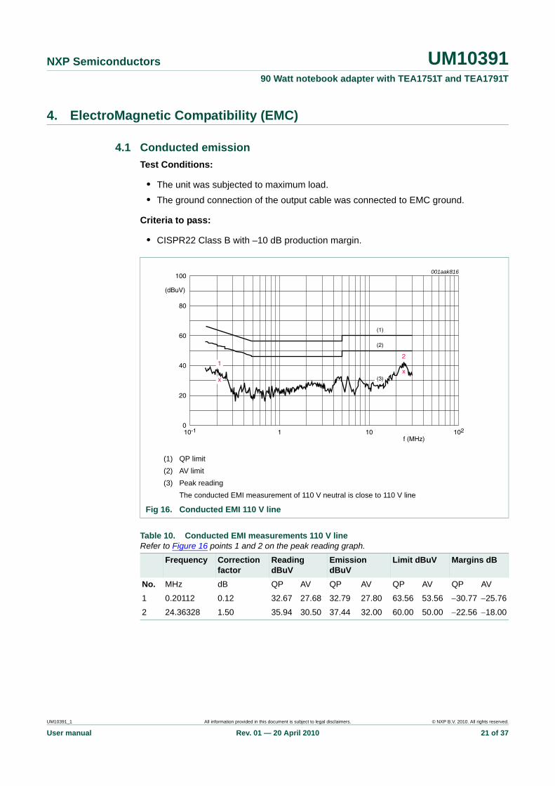
4. ElectroMagnetic Compatibility (EMC)
4.1 Conducted emissionTest Conditions:
• The unit was subjected to maximum load.• The ground connection of the output cable was connected to EMC ground.
Criteria to pass:
• CISPR22 Class B with –10 dB production margin.
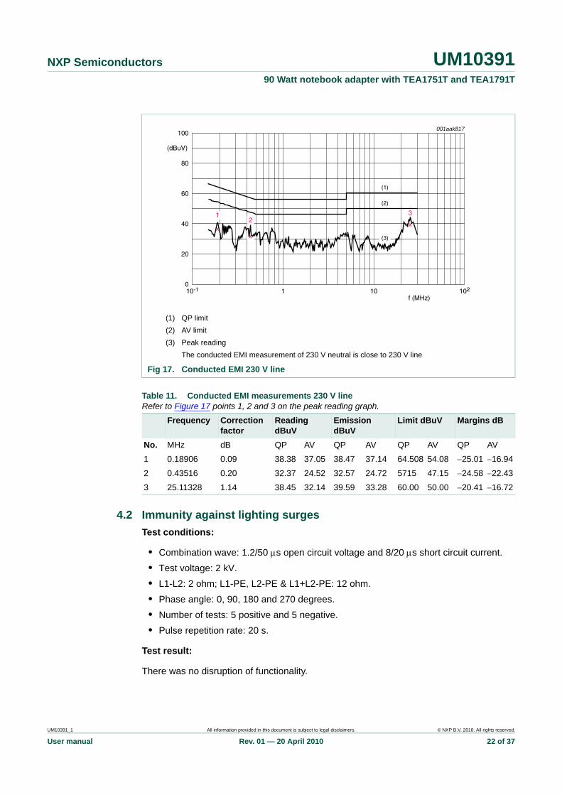
(1) QP limit(2) AV limit(3) Peak reading
The conducted EMI measurement of 110 V neutral is close to 110 V line
Fig 16. Conducted EMI 110 V line
Table 10. Conducted EMI measurements 110 V line Refer to Figure 16 points 1 and 2 on the peak reading graph.
Frequency Correction factor
Reading dBuV
Emission dBuV
Limit dBuV Margins dB
No. MHz dB QP AV QP AV QP AV QP AV
1 0.20112 0.12 32.67 27.68 32.79 27.80 63.56 53.56 −30.77 −25.76
2 24.36328 1.50 35.94 30.50 37.44 32.00 60.00 50.00 −22.56 −18.00
001aak816
f (MHz)10-1 102101
40
60
20
80
100
(dBuV)
0
(1)
(2)
(3)x
2
x
1
UM10391_1 All information provided in this document is subject to legal disclaimers. © NXP B.V. 2010. All rights reserved.
User manual Rev. 01 — 20 April 2010 21 of 37
NXP Semiconductors UM1039190 Watt notebook adapter with TEA1751T and TEA1791T
4.2 Immunity against lighting surgesTest conditions:
• Combination wave: 1.2/50 μs open circuit voltage and 8/20 μs short circuit current.• Test voltage: 2 kV.• L1-L2: 2 ohm; L1-PE, L2-PE & L1+L2-PE: 12 ohm.• Phase angle: 0, 90, 180 and 270 degrees.• Number of tests: 5 positive and 5 negative.• Pulse repetition rate: 20 s.
Test result:
There was no disruption of functionality.
(1) QP limit(2) AV limit(3) Peak reading
The conducted EMI measurement of 230 V neutral is close to 230 V line
Fig 17. Conducted EMI 230 V line
Table 11. Conducted EMI measurements 230 V line Refer to Figure 17 points 1, 2 and 3 on the peak reading graph.
Frequency Correction factor
Reading dBuV
Emission dBuV
Limit dBuV Margins dB
No. MHz dB QP AV QP AV QP AV QP AV
1 0.18906 0.09 38.38 37.05 38.47 37.14 64.508 54.08 −25.01 −16.94
2 0.43516 0.20 32.37 24.52 32.57 24.72 5715 47.15 −24.58 −22.43
3 25.11328 1.14 38.45 32.14 39.59 33.28 60.00 50.00 −20.41 −16.72
001aak817
f (MHz)10-1 102101
40
60
20
80
100
(dBuV)
0
(3)
(2)
(1)
x
1
x
2x
3
UM10391_1 All information provided in this document is subject to legal disclaimers. © NXP B.V. 2010. All rights reserved.
User manual Rev. 01 — 20 April 2010 22 of 37

NXP Semiconductors UM1039190 Watt notebook adapter with TEA1751T and TEA1791T
4.3 Immunity against ESDTest conditions:
• ESD air discharge at the ground terminal of the output cable connector.
Criteria to pass:
• IEC61000-4-2 air discharge level 3 (8 kV) and level 4 (15 kV).
4.4 Mains harmonic reductionTest conditions:
• The unit was set to maximum load.• The input voltage was 230 V / 50 Hz.
Criteria to pass:
• Compliance with EN61000-3-2 A14 class D.
Test result:
Passed, see Figure 18 and Figure 19.
Table 12. Immunity against ESD Performance of the adapter at an ESD air discharge
ESD performance No disruption of function Auto recoveryDemo board according to schematic ± 12 kV ± 15 kV
Demo board with 6 x 10 M across Y-cap ± 16.5 kV -
UM10391_1 All information provided in this document is subject to legal disclaimers. © NXP B.V. 2010. All rights reserved.
User manual Rev. 01 — 20 April 2010 23 of 37

NXP Semiconductors UM1039190 Watt notebook adapter with TEA1751T and TEA1791T
Fig 18. Mains harmonic currents; absolute values
Fig 19. Mains harmonic currents; graphic representation
001aak818
001aak819
UM10391_1 All information provided in this document is subject to legal disclaimers. © NXP B.V. 2010. All rights reserved.
User manual Rev. 01 — 20 April 2010 24 of 37

xxxx xxxxxxxxxxxxxxxxxxxxxxxxxxxxxx x xxxxxxxxxxxxxx xxxxxxxxxx xxx xxxxxx xxxxxxxxxxxxxxxxxxxxxxx xxxxxxxxxxxxxxxxxxxxxx xxxxx xxxxxx xx xxxxxxxxxxxxxxxxxxxxxxxxxxxxx xxxxxxxxxxxxxxxxxxxxxx xxxxxxxxxxx xxxxxxx xxxxxxxxxxxxxxxxxxx xxxxxxxxxxxxxxxx xxxxxxxxxxxxxx xxxxxx xx xxxxxxxxxxxxxxxxxxxxxxxxxxxxxxxx xxxxxxxxxxxxxxxxxxxxxxxx xxxxxxx xxxxxxxxxxxxxxxxxxxxxxxxxxxxxxxxxxxxxxxxxxxxxx xxxxxxxxxxx xxxxx x x
UM
10391_1
User m
anual
NXP Sem
iconducto
5. Schem
atic d
rsU
M10391
90 Watt notebook adapter w
ith TEA1751T and TEA
1791T
iagram
001aak825
R32
C27 C28 C29
C18
R25
31 L3
3567
SR
SE
NS
E
Vout+
Vout−
n.c.n.c.n.c.n.c.1
1T
All information provided in this docum
ent is subject to legal disclaimers.
© N
XP B.V. 2010. All rights reserved.
Rev. 01 —
20 April 2010
25 of 37
Fig 20. Schematic of 90 W TEA1751T and TEA1791T adapter solution
C19C21
C2
C22D27A
C18
C14
C4
C9
C8
C30
R30
Q4
D3
R18
C23
C13
C3AC3
C15
U2
C17
C20 R26
R15A R15
R10
RT2NTC
R4
R7
R5A
R5
R23A D23A
R25
R20
C12
R33 C
R35
C35 R36
R6
BC1D1
C34
C10
C6
U4
R34
R38
R37
C16
R24
R3
CY1 BC2
R27
R23
R16
R22
R17
R16A
R1
F1 RT1NTC
CX1
R2
R14 R13
D4
T1D30
C1BD1
+
−
R9 R8
R12 R11
D2
L2L1
LF2
Q2
C5Q1
D5
14
7
11PFCSENSE
12PFCDRIVER
8PFCAUX
FBAUX4
FBCTRL3
4
3
5
1
4
2 11
7, 8
9, 10
8
2
DR
IVE
R
4
VCC
GND
9
12
7
1
6
1
2
PFCCOMP6
HV
S
15
HV
S
9
VO
SE
NS
E
13
FB
DR
IVE
R
10
FB
SE
NS
E
16H
V1
VC
C
VIN
SE
NS
E
2
GN
D
5
LAT
CH
U1
TEA1751T
U3
TEA179
LF1
MAINS INLET
Θ
Θ

NXP Semiconductors UM1039190 Watt notebook adapter with TEA1751T and TEA1791T
6. Bill of materials
Table 13. Default bill of materials for a 90 W TEA1751T and TEA1791T adapter solution Reference Component Package RemarkR1 2 MΩ, 1 % 1206
R2 2 MΩ, 1 % 1206
R3 560 kΩ, 1 % 1206
R4 47 kΩ, 1 % 0603
R5 3.3 MΩ, 1 % 1206
R5A 3.3 MΩ, 1 % 1206
R6 2.7 MΩ, 1 % 1206
R7 60.4 kΩ, 1 % 0603
R8 10 Ω, 5 % 0805
R9 10 Ω, 5 % 0805
R10 0.1 Ω, 5 %, 1 W Axial metal oxide film
R11 15 kΩ, 5 % 0603
R12 1 kΩ, 5 % 0805
R13 10 Ω, 5 % 0805
R14 10 Ω, 5 % 0805
R15 0.1 Ω, 5 %, 1 W Axial metal oxide film
R15A 0.3 Ω, 1 % RL1632
R16 27 kΩ, 5 % 0603
R16A 750 Ω, 5 % 0603
R17 1 kΩ, 5 % 0603
R18 43 kΩ, 5 % 1206
R19 43 kΩ, 5 % 1206
R20 47 Ω, 5 % 0805
R21 0 Ω 0805
R22 10 kΩ, 5 % 0805
R23 82 kΩ, 1 % 0603
R23A 47 kΩ, 1 % 0603
R24 39 kΩ, 5 % 0603
R25 39 kΩ, 5 % 0603
R26 10 kΩ, 5 % 0603
R27 5.1 kΩ, 5 % 1206
R30 10 Ω, 5 % 0805
R32 1 kΩ, 5 % 0805
R33 Not Mounted
R34 1 kΩ, 5 % 0603
R35 2.7 kΩ, 5 % 0603
R36 10 kΩ, 5 % 0603
R37 35.7 kΩ, 1 % 0603
R38 5.23 kΩ, 1 % 0603
UM10391_1 All information provided in this document is subject to legal disclaimers. © NXP B.V. 2010. All rights reserved.
User manual Rev. 01 — 20 April 2010 26 of 37
NXP Semiconductors UM1039190 Watt notebook adapter with TEA1751T and TEA1791T
R39 not mounted
RT1 Jumper
RT2 NTC 100 kΩ, D = 5 mm Radial lead TTC050104
C1 Film capacitor 0.47 μF / 450 V, 10 %
C2 Film capacitor 0.47 μF / 450V, 10 %
C3 Electrolytic capacitor 100 μF / 400V, 105 °C
Radial 16x30 mm
C3A 10 nF / 1 kV, Z5U Disk 11.5 mm
C4 10 nF / 25 V, X7R 0603
C5 220 pF / 630 V, NP0 1206
C6 0.1 μF / 25 V, X7R 0603
C8 3300 pF / 630 V 1206
C9 100 pF / 630 V, NP0 1206
C10 0.1 μF / 25 V, X7R 0805
C12 220 pF / 100 V, NP0 0805
C13 Electrolytic capacitor 47 μF / 35V, 105 °C
Radial 5 x 11 mm low impedance type
C14 1 μF / 50 V, Y5V 0805
C15 10 nF / 25 V, X7R 0603
C16 0.33 μF / 10 V, X7R 0603 timing capacitor; review tolerance
C17 0.33 μF / 10 V, X7R 0603
C18 0.47 μF / 10 V, X7R 0603
C19 10 nF / 25 V, X7R 0603
C20 2.2 μF / 10 V, Y5V 0603
C21 2.2 μF / 10 V, Y5V 0603
C22 220 pF / 50 V, NP0 0603 10 V is permitted
C23 220 pF / 50 V, NP0 0603 10 V is permitted
C27 Electrolytic capacitor 470 μF / 25V, 105 °C
Radial 10 x 12.5 mm low impedance type
C28 Electrolytic capacitor 470 μF / 25V, 105 °C
Radial 10 x 12.5 mm low impedance type
C29 Electrolytic capacitor 470 μF / 25V, 105 °C
Radial 10 x 12.5 mm low impedance type
C30 1 μF / 50 V, Y5V 0805
C31 Not mounted
C34 0.1 μF / 25 V, X7R 0603
C35 10 nF / 25 V, X7R 0603
C36 Not mounted
CX1 0.33 μF / 275 V AC, X2 MKP
CY1 1000 pF / 400 V AC, Y1 Pitch 10 mm
Table 13. Default bill of materials for a 90 W TEA1751T and TEA1791T adapter solution …continued
Reference Component Package Remark
UM10391_1 All information provided in this document is subject to legal disclaimers. © NXP B.V. 2010. All rights reserved.
User manual Rev. 01 — 20 April 2010 27 of 37
NXP Semiconductors UM1039190 Watt notebook adapter with TEA1751T and TEA1791T
BD1 GBU806, 8 A / 600 V Flat / mini
D1 MUR460, 4 A / 600 V DO-201AD Vishay
D2 1N4148W SOD-123
D3 S2M SMB
D4 1N4148W SOD-123
D5 BAS21 SOT23 NXP, BAS20 is permitted
D23A BAS21 SOT23 NXP, BAS20 is permitted
D27A 1N4148W SOD-123
D30 BAS21 SOT23 NXP
Q1 2SK3568 TO220F
Q2 2SK3569 TO220F
Q4 PSMN015-100P TO220 NXP
U1 TEA1751T SO16 NXP, GreenChip III PFC + flyback controller
U2 LTV817B DIP4-W CTR 130-260, spacing 10.16 mm
U3 TEA1791T SO8 NXP, GreenChip-SR controller
U4 AP431SR SOT-23R diodes
T1 Flyback transformer 450 μH PQ3220 see specification
L1 Inductor 210 μH T50-52
L2 PFC inductor 250 μH RM10 see specification
L3 Inductor CM 200 μH T12*6*4
LF1 Inductor CM 500 μH T12*6*4
LF2 Inductor CM 12.8 MH T16*12*18
BC1 Bead core R5B/XP N4/AMAX RH 4*6*2 placed at cathode of D1
BC2 Bead core S6H/JK N6/AMAX RH 3.5*4.2*1.3 placed at lead of CY1
F1 Fuse T3, 15 A / 250 V LT5
Table 13. Default bill of materials for a 90 W TEA1751T and TEA1791T adapter solution …continued
Reference Component Package Remark
UM10391_1 All information provided in this document is subject to legal disclaimers. © NXP B.V. 2010. All rights reserved.
User manual Rev. 01 — 20 April 2010 28 of 37

NXP Semiconductors UM1039190 Watt notebook adapter with TEA1751T and TEA1791T
7. Transformer and inductor specifications
7.1 Flyback transformer T1 specifications
• Primary inductance: 450 μH (±±5 %).• Leakage inductance: 6 μH (max).• Core / Bobbin: PQ3220.• Core material: PC44.• HI-POT prim - sec: 3 kV / 5 mA, 3 sec.
Manufacturer: Send Power Electronics. Co., LTD, Taiwan ROC.
Fig 21. Flyback transformer schematic
Teflon tube
Start
E1, E2, E3, E4
N1, N67
9
10
8
11
2
4
1
5
6
N4, N7
N8
N5
N2
N3
Black teflon tube
Primary Secondary
Bobbin
N1
Tape
N2
N3
N4
E2
N5
N6
N7
N8
E1
E4
E3
014aab118
Table 14. Flyback transformer winding detailsWinding order
Pin number Wire type Number of wires
Number of turns RemarksStart Finish Winding MYLAR tape
1: N1 7 9 TEX-E (3L) 0.3 mm ∅ 2 6 1
2: E1 6 Copper foil 0.025 mm x 7 mm 1 1 finished with wire 0.3 ∅
3: N2 1 4 2-UEW 0.5 mm ∅ 1 16 1
4: E2 6 Copper foil 0.025 mm x 7 mm 1 1 finished with wire 0.3 ∅
5: N3 5 6 2-UEW 0.25 mm ∅ 2 7 1
6: N4 8 10 TEX-E (3L) 0.3 mm ∅ 2 6 1
7: E3 6 Copper foil 0.025 mm x 7 mm 1 1 finished with wire 0.3 ∅
8: N5 4 2 2-UEW 0.5 mm ∅ 1 16 1
9: E4 6 Copper foil 0.025 mm x 7 mm 1 1 finished with wire 0.3 ∅
10: N6 7 9 TEX-E (3L) 0.3 mm ∅ 2 6 1
11: N7 8 10 TEX-E (3L) 0.3 mm ∅ 2 6 1
12: N8 11 8 TEX-E (3L) 0.3 mm ∅ 1 5 3 close winding method
UM10391_1 All information provided in this document is subject to legal disclaimers. © NXP B.V. 2010. All rights reserved.
User manual Rev. 01 — 20 April 2010 29 of 37
NXP Semiconductors UM1039190 Watt notebook adapter with TEA1751T and TEA1791T
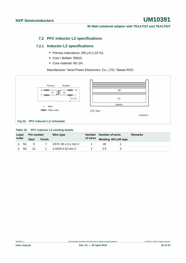
7.2 PFC inductor L2 specifications
7.2.1 Inductor L2 specifications
• Primary inductance: 250 μH (±10 %).• Core / Bobbin: RM10.• Core material: NC-2H.
Manufacturer: Send Power Electronics. Co., LTD, Taiwan ROC.
Fig 22. PFC inductor L2 schematic
Teflon tube
Start
E1, E2
N212
1
9
7N1
Primary Auxilary
Bobbin
N1
Tape
N2
014aab121
Table 15. PFC inductor L2 winding detailsLayer order
Pin number Wire type Number of wires
Number of turns RemarksStart Finish Winding MYLAR tape
1: N1 9 7 USTC 30 x 0.1 mm ∅ 1 40 1
2: N2 12 1 2-UEW 0.22 mm ∅ 2 2.5 3
UM10391_1 All information provided in this document is subject to legal disclaimers. © NXP B.V. 2010. All rights reserved.
User manual Rev. 01 — 20 April 2010 30 of 37
NXP Semiconductors UM1039190 Watt notebook adapter with TEA1751T and TEA1791T
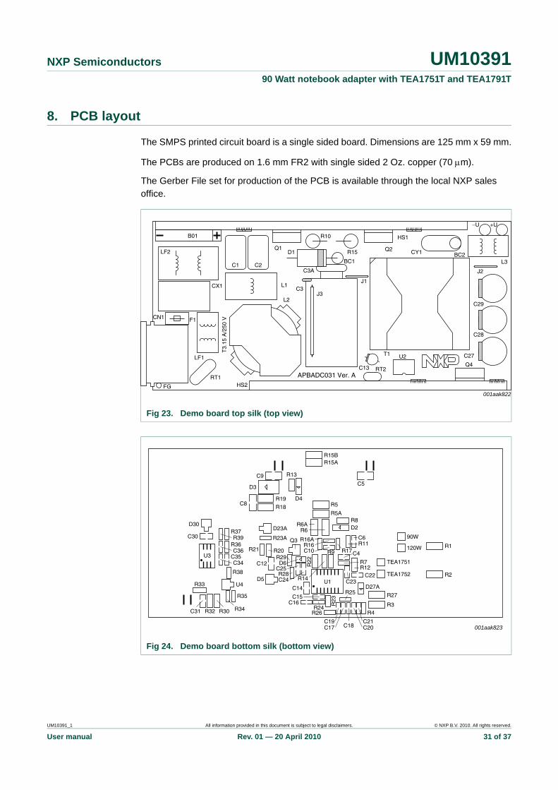
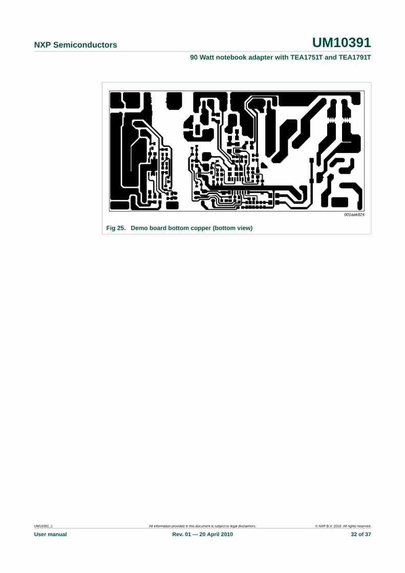
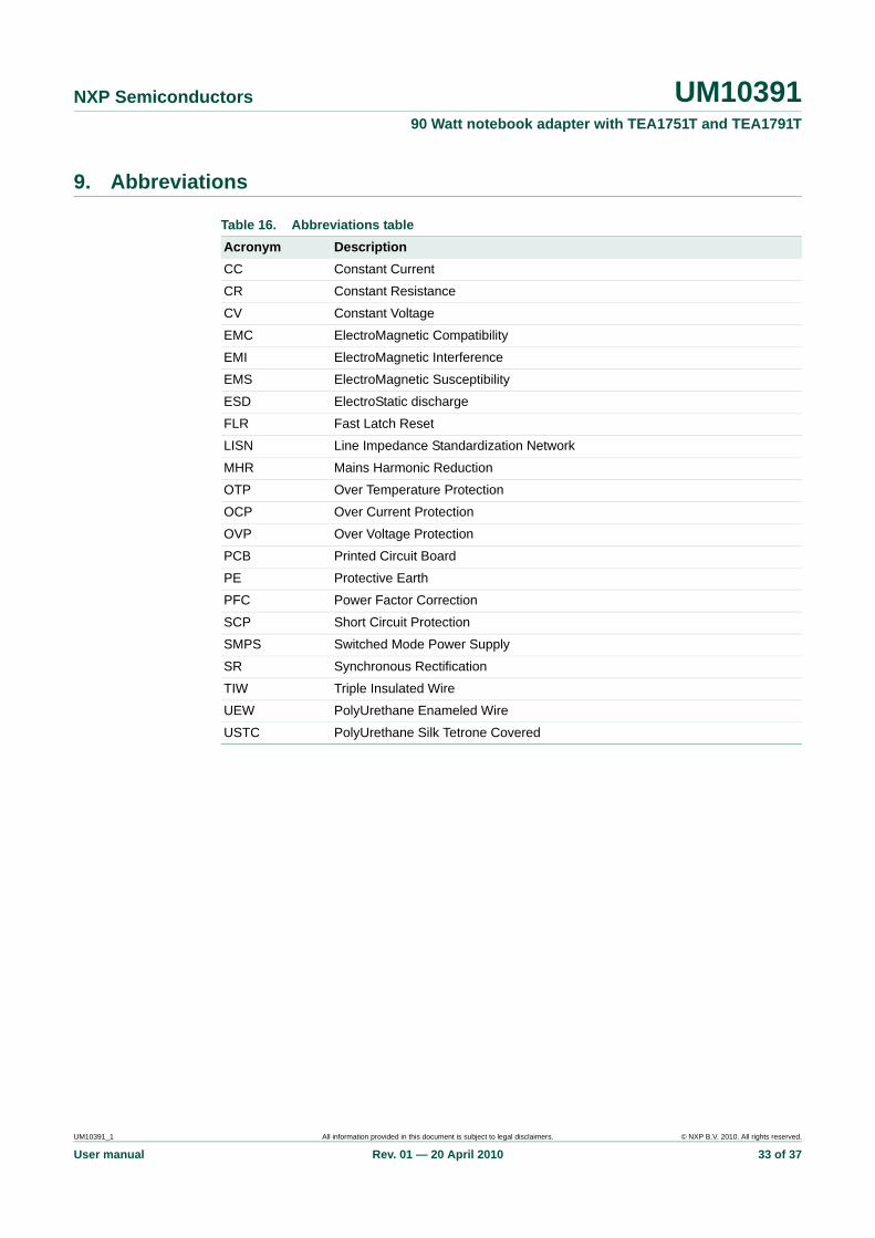
8. PCB layout
The SMPS printed circuit board is a single sided board. Dimensions are 125 mm x 59 mm.
The PCBs are produced on 1.6 mm FR2 with single sided 2 Oz. copper (70 μm).
The Gerber File set for production of the PCB is available through the local NXP sales office.
Fig 23. Demo board top silk (top view)
Fig 24. Demo board bottom silk (bottom view)
001aak822
R10
D1Q1
C2C1
CX1
B01
LF2
CN1 F1
FG
RT1HS2
LF1
L2
APBADC031 Ver. A
−U +UT
3.15
A/2
50 V
C3L1
C3A
J3
BC1
R15
J1
C13 RT2
T1 U2Q4
C27
C28
C29
J2
L3BC2CY1Q2
HS1
001aak823
R13
C8
D3
C9
R21
C12
D5
R29
R6AR6
R16AR16C10
D6C25R28C24 R14
C14
C15
C19C17 C18
C21C20
C16
R26R24
R23
D30
C30
U3
Q3
D4
R33
C31 R32 R30
R18
R19
R37
R36
C35
R39
C36
C34
R38
U4
R35
R34
D23A
R23A
R20
R15BR15A
R5
R5AR8D2
R1
R2
90W
120W
TEA1751
TEA1752
R27
R3R4
D27A
C22R12R7
R9
C23
R25
U1
R22
C6R11
R17C4
C5
UM10391_1 All information provided in this document is subject to legal disclaimers. © NXP B.V. 2010. All rights reserved.
User manual Rev. 01 — 20 April 2010 31 of 37
NXP Semiconductors UM1039190 Watt notebook adapter with TEA1751T and TEA1791T
Fig 25. Demo board bottom copper (bottom view)
001aak824
UM10391_1 All information provided in this document is subject to legal disclaimers. © NXP B.V. 2010. All rights reserved.
User manual Rev. 01 — 20 April 2010 32 of 37
NXP Semiconductors UM1039190 Watt notebook adapter with TEA1751T and TEA1791T
9. Abbreviations
Table 16. Abbreviations tableAcronym DescriptionCC Constant Current
CR Constant Resistance
CV Constant Voltage
EMC ElectroMagnetic Compatibility
EMI ElectroMagnetic Interference
EMS ElectroMagnetic Susceptibility
ESD ElectroStatic discharge
FLR Fast Latch Reset
LISN Line Impedance Standardization Network
MHR Mains Harmonic Reduction
OTP Over Temperature Protection
OCP Over Current Protection
OVP Over Voltage Protection
PCB Printed Circuit Board
PE Protective Earth
PFC Power Factor Correction
SCP Short Circuit Protection
SMPS Switched Mode Power Supply
SR Synchronous Rectification
TIW Triple Insulated Wire
UEW PolyUrethane Enameled Wire
USTC PolyUrethane Silk Tetrone Covered
UM10391_1 All information provided in this document is subject to legal disclaimers. © NXP B.V. 2010. All rights reserved.
User manual Rev. 01 — 20 April 2010 33 of 37
NXP Semiconductors UM1039190 Watt notebook adapter with TEA1751T and TEA1791T
10. Legal information
10.1 DefinitionsDraft — The document is a draft version only. The content is still under internal review and subject to formal approval, which may result in modifications or additions. NXP Semiconductors does not give any representations or warranties as to the accuracy or completeness of information included herein and shall have no liability for the consequences of use of such information.
10.2 DisclaimersLimited warranty and liability — Information in this document is believed to be accurate and reliable. However, NXP Semiconductors does not give any representations or warranties, expressed or implied, as to the accuracy or completeness of such information and shall have no liability for the consequences of use of such information.
In no event shall NXP Semiconductors be liable for any indirect, incidental, punitive, special or consequential damages (including - without limitation - lost profits, lost savings, business interruption, costs related to the removal or replacement of any products or rework charges) whether or not such damages are based on tort (including negligence), warranty, breach of contract or any other legal theory.
Notwithstanding any damages that customer might incur for any reason whatsoever, NXP Semiconductors’ aggregate and cumulative liability towards customer for the products described herein shall be limited in accordance with the Terms and conditions of commercial sale of NXP Semiconductors.
Right to make changes — NXP Semiconductors reserves the right to make changes to information published in this document, including without limitation specifications and product descriptions, at any time and without notice. This document supersedes and replaces all information supplied prior to the publication hereof.
Suitability for use — NXP Semiconductors products are not designed, authorized or warranted to be suitable for use in medical, military, aircraft, space or life support equipment, nor in applications where failure or malfunction of an NXP Semiconductors product can reasonably be expected to result in personal injury, death or severe property or environmental damage. NXP Semiconductors accepts no liability for inclusion and/or use of NXP Semiconductors products in such equipment or applications and therefore such inclusion and/or use is at the customer’s own risk.
Applications — Applications that are described herein for any of these products are for illustrative purposes only. NXP Semiconductors makes no representation or warranty that such applications will be suitable for the specified use without further testing or modification.
NXP Semiconductors does not accept any liability related to any default, damage, costs or problem which is based on a weakness or default in the customer application/use or the application/use of customer’s third party customer(s) (hereinafter both referred to as “Application”). It is customer’s sole responsibility to check whether the NXP Semiconductors product is suitable and fit for the Application planned. Customer has to do all necessary testing for the Application in order to avoid a default of the Application and the product. NXP Semiconductors does not accept any liability in this respect.
Export control — This document as well as the item(s) described herein may be subject to export control regulations. Export might require a prior authorization from national authorities.
10.3 TrademarksNotice: All referenced brands, product names, service names and trademarks are the property of their respective owners.
GreenChip — is a trademark of NXP B.V.
UM10391_1 All information provided in this document is subject to legal disclaimers. © NXP B.V. 2010. All rights reserved.
User manual Rev. 01 — 20 April 2010 34 of 37
NXP Semiconductors UM1039190 Watt notebook adapter with TEA1751T and TEA1791T
11. Tables
Table 1. Efficiency PFC plus flyback stage . . . . . . . . . . .5Table 2. Active mode efficiency at 115 V / 60 Hz . . . . . .6Table 3. Active mode efficiency at 230 V / 50 Hz . . . . . .6Table 4. No-load input power . . . . . . . . . . . . . . . . . . . . .6Table 5. Output over-voltage protection . . . . . . . . . . . .14Table 6. Load regulation . . . . . . . . . . . . . . . . . . . . . . . .17Table 7. Line regulation . . . . . . . . . . . . . . . . . . . . . . . . .18Table 8. Ripple and noise P.A.R.D. . . . . . . . . . . . . . . . .18Table 9. Dynamic load response . . . . . . . . . . . . . . . . . .20Table 10. Conducted EMI measurements 110 V line . . .21Table 11. Conducted EMI measurements 230 V line . . .22Table 12. Immunity against ESD . . . . . . . . . . . . . . . . . . .23Table 13. Default bill of materials for a 90 W
TEA1751T and TEA1791T adapter solution . .26Table 14. Flyback transformer winding details . . . . . . . . .29Table 15. PFC inductor L2 winding details . . . . . . . . . . . .30Table 16. Abbreviations table . . . . . . . . . . . . . . . . . . . . . .33
UM10391_1 All information provided in this document is subject to legal disclaimers. © NXP B.V. 2010. All rights reserved.
User manual Rev. 01 — 20 April 2010 35 of 37

NXP Semiconductors UM1039190 Watt notebook adapter with TEA1751T and TEA1791T
12. Figures
Fig 1. 90 W TEA1751T and TEA1791T demo board . . . .3Fig 2. Delay between switch-on and output in
regulation . . . . . . . . . . . . . . . . . . . . . . . . . . . . . . . .7Fig 3. Output rise time at full load start-up . . . . . . . . . . . .8Fig 4. Brownout and brownout recovery . . . . . . . . . . . . .9Fig 5. Normal start-up at 90 V / 60 Hz . . . . . . . . . . . . . .10Fig 6. Normal start-up at 264 V / 50 Hz . . . . . . . . . . . . .10Fig 7. Output short-circuit at 90 V / 60 Hz . . . . . . . . . . . 11Fig 8. Output short-circuit at 264 V / 50 Hz . . . . . . . . . .12Fig 9. Output short-circuit protection . . . . . . . . . . . . . . .12Fig 10. Output over current protection . . . . . . . . . . . . . . .13Fig 11. Output over-voltage protection. . . . . . . . . . . . . . .14Fig 12. External Over Temperature Protection (OTP) . . .15Fig 13. Fast Latch Reset (FLR) . . . . . . . . . . . . . . . . . . . .16Fig 14. Ripple and noise . . . . . . . . . . . . . . . . . . . . . . . . .19Fig 15. Dynamic load response . . . . . . . . . . . . . . . . . . . .20Fig 16. Conducted EMI 110 V line . . . . . . . . . . . . . . . . . .21Fig 17. Conducted EMI 230 V line . . . . . . . . . . . . . . . . . .22Fig 18. Mains harmonic currents; absolute values. . . . . .24Fig 19. Mains harmonic currents; graphic
representation . . . . . . . . . . . . . . . . . . . . . . . . . . .24Fig 20. Schematic of 90 W TEA1751T and TEA1791T
adapter solution . . . . . . . . . . . . . . . . . . . . . . . . . .25Fig 21. Flyback transformer schematic . . . . . . . . . . . . . .29Fig 22. PFC inductor L2 schematic . . . . . . . . . . . . . . . . .30Fig 23. Demo board top silk (top view) . . . . . . . . . . . . . .31Fig 24. Demo board bottom silk (bottom view) . . . . . . . .31Fig 25. Demo board bottom copper (bottom view). . . . . .32
UM10391_1 All information provided in this document is subject to legal disclaimers. © NXP B.V. 2010. All rights reserved.
User manual Rev. 01 — 20 April 2010 36 of 37
NXP Semiconductors UM1039190 Watt notebook adapter with TEA1751T and TEA1791T
13. Contents
1 Introduction . . . . . . . . . . . . . . . . . . . . . . . . . . . . 32 Specification. . . . . . . . . . . . . . . . . . . . . . . . . . . . 43 Performance data. . . . . . . . . . . . . . . . . . . . . . . . 43.1 Test setup . . . . . . . . . . . . . . . . . . . . . . . . . . . . . 43.1.1 Test equipment . . . . . . . . . . . . . . . . . . . . . . . . . 43.1.2 Test conditions . . . . . . . . . . . . . . . . . . . . . . . . . 43.2 Efficiency . . . . . . . . . . . . . . . . . . . . . . . . . . . . . 53.2.1 Efficiency PFC plus flyback stage. . . . . . . . . . . 53.2.2 Energy Star efficiency . . . . . . . . . . . . . . . . . . . . 53.2.2.1 Active mode efficiency . . . . . . . . . . . . . . . . . . . 53.2.2.2 No-load input power . . . . . . . . . . . . . . . . . . . . . 63.3 Timing and protection . . . . . . . . . . . . . . . . . . . . 73.3.1 Switch-on delay and output rise time . . . . . . . . 73.3.2 Brownout and brownout recovery. . . . . . . . . . . 83.3.3 Output short circuit and open loop protection. . 93.3.3.1 Open loop protection . . . . . . . . . . . . . . . . . . . . 93.3.3.2 Short-circuit protection . . . . . . . . . . . . . . . . . . 113.3.4 Over-current protection. . . . . . . . . . . . . . . . . . 133.3.5 Output Over-Voltage Protection (OVP). . . . . . 133.3.6 Over-temperature protection . . . . . . . . . . . . . 153.3.7 Fast latch reset . . . . . . . . . . . . . . . . . . . . . . . . 153.4 Output regulation and characterization. . . . . . 173.4.1 Load regulation. . . . . . . . . . . . . . . . . . . . . . . . 173.4.2 Line regulation . . . . . . . . . . . . . . . . . . . . . . . . 173.4.3 Ripple and noise PARD. (Periodic And
Random Deviation) . . . . . . . . . . . . . . . . . . . . . 183.4.4 Dynamic load response . . . . . . . . . . . . . . . . . 204 ElectroMagnetic Compatibility (EMC) . . . . . . 214.1 Conducted emission . . . . . . . . . . . . . . . . . . . . 214.2 Immunity against lighting surges . . . . . . . . . . 224.3 Immunity against ESD . . . . . . . . . . . . . . . . . . 234.4 Mains harmonic reduction . . . . . . . . . . . . . . . 235 Schematic diagram . . . . . . . . . . . . . . . . . . . . . 256 Bill of materials . . . . . . . . . . . . . . . . . . . . . . . . 267 Transformer and inductor specifications . . . 297.1 Flyback transformer T1 specifications . . . . . . 297.2 PFC inductor L2 specifications . . . . . . . . . . . . 307.2.1 Inductor L2 specifications . . . . . . . . . . . . . . . . 308 PCB layout . . . . . . . . . . . . . . . . . . . . . . . . . . . . 319 Abbreviations. . . . . . . . . . . . . . . . . . . . . . . . . . 3310 Legal information. . . . . . . . . . . . . . . . . . . . . . . 3410.1 Definitions. . . . . . . . . . . . . . . . . . . . . . . . . . . . 3410.2 Disclaimers . . . . . . . . . . . . . . . . . . . . . . . . . . . 3410.3 Trademarks. . . . . . . . . . . . . . . . . . . . . . . . . . . 3411 Tables . . . . . . . . . . . . . . . . . . . . . . . . . . . . . . . . 3512 Figures . . . . . . . . . . . . . . . . . . . . . . . . . . . . . . . 36
13 Contents. . . . . . . . . . . . . . . . . . . . . . . . . . . . . . 37
© NXP B.V. 2010. All rights reserved.For more information, please visit: http://www.nxp.com For sales office addresses, please send an email to: [email protected]
Date of release: 20 April 2010Document identifier: UM10391_1
Please be aware that important notices concerning this document and the product(s) described herein, have been included in section ‘Legal information’.
Related Documents