nature photonics | VOL 2 | FEBRUARY 2008 | www.nature.com/naturephotonics 77 REVIEW ARTICLE ASIF KHAN, KRISHNAN BALAKRISHNAN AND TOM KATONA Department of Electrical Engineering, University of South Carolina, Columbia, South Carolina 29208, USA e-mail: [email protected] Research and development on III-nitride semiconductors gained momentum much later than other conventional semiconductors such as silicon and gallium arsenide. is was due to the difficulty in fabricating high-quality bulk III-nitride crystals and their epitaxial layers. Although initial synthesis of AlN, InN and GaN was reported in the early twentieth century, adequate quality for device fabrication has only been achieved in the past two decades. Despite the fact that the III-nitride materials have a direct bandgap, suitable for high- efficiency generation of green, blue and violet light to complete the visible colour spectrum, research was limited owing to the lack of a suitably lattice-matched substrate and the difficulty of incorporating nitrogen into the semiconductor lattice 1 . Aſter decades of research on GaN and its ternary alloys InGaN and AlGaN, experimental procedures were developed that enabled the growth of high-quality single-crystal materials by using a low-temperature nucleation layer 2,3 . Shortly aſterwards, p-type GaN was realized using low-energy electron-beam treatment of the magnesium-doped material, followed by thermal annealing 4,5 . ese two advancements began a period of tremendous growth and rapid progress in the development of III- nitride violet/blue/green/white LEDs and violet laser diodes. With AlInGaP-based red and yellow LEDs already available, this completed the colour spectrum that could be achieved using semiconductor sources. ‘Visible’ light-emission device technology is reaching its maturity, and many groups have shiſted their research focus towards the shorter-wavelength UV devices. is interest is fuelled by the potential applications for these UV LEDs in air- and water- purification, germicidal and biomedical instrumentation systems 6 . ese combined markets are worth in excess of several billion dollars, which provides a strong impetus for research. Here, the progress of III-nitride-based UV and deep-UV LEDs is reviewed. Challenges associated with the growth and fabrication of AlInGaN-based Ultraviolet light-emitting diodes based on group three nitrides Light-emitting diodes with emission wavelengths less than 400 nm have been developed using the AlInGaN material system. For devices operating at shorter wavelengths, alloy compositions with a greater aluminium content are required. The material properties of these materials lie on the border between conventional semiconductors and insulators, which adds a degree of complexity to the development of efficient light-emitting devices. A number of technical developments have enabled the fabrication of LEDs based on group three nitrides (III-nitrides) that emit in the UV part of the spectrum, providing useful tools for a wealth of applications in optoelectronic systems. light-emission devices are presented, and the methods that have been used to overcome them are discussed. In addition, we also present an overview of key areas of future research that have the potential to enable the next generation of UV-emitting devices. e electromagnetic spectrum is divided into regions based on the wavelength of the radiation, with the UV region defined as the wavelength range from 10 nm to 400 nm. e UV spectrum is further subdivided into four distinct regions: UV-A or long-wave UV (320–400 nm); UV-B or mid-wave UV (290–320 nm); UV-C or short-wave UV (200–290 nm); and vacuum UV (10–200 nm). e emission wavelength is dictated by the fundamental bandgap of the material used in the active region of the device. us in principle III-nitride LEDs can emit from about 200 nm (the bandgap of AlN) to about 400 nm (the bandgap of InGaN), thus spanning the entire UV-A, -B and -C regions. So far LEDs emitting at 210–400 nm have already been demonstrated (Box 1). LONG-WAVE ULTRAVIOLET e UV-A region can be further divided into two subregions based on whether the emission wavelength is greater than, or less than about 365 nm (the bandgap of GaN). Light-emitting diodes with an emission wavelength longer than 365 nm typically have GaN or InGaN quantum wells (QWs) in the active region, and those with shorter wavelengths in general have AlGaN QWs. In this section, we discuss the differences in the design and manufacture of these two types of devices and the state-of-the-art performance of each. e growth and fabrication technology for UV-A LEDs with emission at wavelengths longer than 365 nm is fairly mature. is is a result of their simultaneous development with visible blue-green light emitters. Owing to the similarity in the recombination mechanisms and device design with those of visible LEDs, UV-A devices were relatively easy to manufacture. ey have found a wide range of applications, such as in counterfeit currency detection, industrial curing and photocatalytic deodorizing, and as pump sources for phosphors to produce white LEDs. Light-emitting diodes operating at 365–400 nm are now widely available. Most of the commercially available devices © 2008 Nature Publishing Group

Welcome message from author
This document is posted to help you gain knowledge. Please leave a comment to let me know what you think about it! Share it to your friends and learn new things together.
Transcript
nature photonics | VOL 2 | FEBRUARY 2008 | www.nature.com/naturephotonics 77
REVIEW ARTICLE
Asif KhAn, KrishnAn BAlAKrishnAn And Tom KATonADepartment of Electrical Engineering, University of South Carolina, Columbia, South Carolina 29208, USA
e-mail: [email protected]
Research and development on III-nitride semiconductors gained momentum much later than other conventional semiconductors such as silicon and gallium arsenide. This was due to the difficulty in fabricating high-quality bulk III-nitride crystals and their epitaxial layers. Although initial synthesis of AlN, InN and GaN was reported in the early twentieth century, adequate quality for device fabrication has only been achieved in the past two decades. Despite the fact that the III-nitride materials have a direct bandgap, suitable for high-efficiency generation of green, blue and violet light to complete the visible colour spectrum, research was limited owing to the lack of a suitably lattice-matched substrate and the difficulty of incorporating nitrogen into the semiconductor lattice1. After decades of research on GaN and its ternary alloys InGaN and AlGaN, experimental procedures were developed that enabled the growth of high-quality single-crystal materials by using a low-temperature nucleation layer2,3. Shortly afterwards, p-type GaN was realized using low-energy electron-beam treatment of the magnesium-doped material, followed by thermal annealing4,5. These two advancements began a period of tremendous growth and rapid progress in the development of III-nitride violet/blue/green/white LEDs and violet laser diodes. With AlInGaP-based red and yellow LEDs already available, this completed the colour spectrum that could be achieved using semiconductor sources. ‘Visible’ light-emission device technology is reaching its maturity, and many groups have shifted their research focus towards the shorter-wavelength UV devices. This interest is fuelled by the potential applications for these UV LEDs in air- and water-purification, germicidal and biomedical instrumentation systems6. These combined markets are worth in excess of several billion dollars, which provides a strong impetus for research. Here, the progress of III-nitride-based UV and deep-UV LEDs is reviewed. Challenges associated with the growth and fabrication of AlInGaN-based
Ultraviolet light-emitting diodes based on group three nitrides
Light-emitting diodes with emission wavelengths less than 400 nm have been developed using the
AlInGaN material system. For devices operating at shorter wavelengths, alloy compositions with a
greater aluminium content are required. The material properties of these materials lie on the border
between conventional semiconductors and insulators, which adds a degree of complexity to the
development of efficient light-emitting devices. A number of technical developments have enabled the
fabrication of LEDs based on group three nitrides (III-nitrides) that emit in the UV part of the spectrum,
providing useful tools for a wealth of applications in optoelectronic systems.
light-emission devices are presented, and the methods that have been used to overcome them are discussed. In addition, we also present an overview of key areas of future research that have the potential to enable the next generation of UV-emitting devices.
The electromagnetic spectrum is divided into regions based on the wavelength of the radiation, with the UV region defined as the wavelength range from 10 nm to 400 nm. The UV spectrum is further subdivided into four distinct regions: UV-A or long-wave UV (320–400 nm); UV-B or mid-wave UV (290–320 nm); UV-C or short-wave UV (200–290 nm); and vacuum UV (10–200 nm). The emission wavelength is dictated by the fundamental bandgap of the material used in the active region of the device. Thus in principle III-nitride LEDs can emit from about 200 nm (the bandgap of AlN) to about 400 nm (the bandgap of InGaN), thus spanning the entire UV-A, -B and -C regions. So far LEDs emitting at 210–400 nm have already been demonstrated (Box 1).
long-wAve ulTrAvioleT
The UV-A region can be further divided into two subregions based on whether the emission wavelength is greater than, or less than about 365 nm (the bandgap of GaN). Light-emitting diodes with an emission wavelength longer than 365 nm typically have GaN or InGaN quantum wells (QWs) in the active region, and those with shorter wavelengths in general have AlGaN QWs. In this section, we discuss the differences in the design and manufacture of these two types of devices and the state-of-the-art performance of each.
The growth and fabrication technology for UV-A LEDs with emission at wavelengths longer than 365 nm is fairly mature. This is a result of their simultaneous development with visible blue-green light emitters. Owing to the similarity in the recombination mechanisms and device design with those of visible LEDs, UV-A devices were relatively easy to manufacture. They have found a wide range of applications, such as in counterfeit currency detection, industrial curing and photocatalytic deodorizing, and as pump sources for phosphors to produce white LEDs.
Light-emitting diodes operating at 365–400 nm are now widely available. Most of the commercially available devices
© 2008 Nature Publishing Group
REVIEW ARTICLE
78 nature photonics | VOL 2 | FEBRUARY 2008 | www.nature.com/naturephotonics
are fabricated from InGaN QWs. It has been demonstrated that the low-indium-composition UV-A LEDs are more sensitive to the threading-dislocation density (TDD) than their higher-indium-composition visible counterparts and several research groups have shown that the external quantum efficiency (EQE) has a large dependence on the number of threading dislocations (refs 7,8). Compared with devices grown on sapphire, UV-A devices on GaN substrates exhibit an increased efficiency. This is a result of the reduction in the TDD owing to the use of low-dislocation-density native-bulk or quasi-bulk substrate material. In addition to the TDD, as the emission wavelength approaches 365 nm GaN and particularly p-type GaN becomes absorbing, which can greatly affect the extraction of light from the semiconductor chip. Light-emitting diodes operating at 365 nm have been developed using a ‘GaN-free’ device structure achieved through laser-assisted lift-off or separation of the GaN from the sapphire substrate, followed by removal of the exposed sapphire substrate (ref. 9). This resulted in 365-nm LEDs with EQEs in excess of 5%, even using conventional metalorganic chemical-vapour deposition (MOCVD) of the GaN on sapphire. Subsequently, it was demonstrated that using the same approach (substrate and GaN removal) but on GaN substrates resulted in an increased efficiency and device lifetime compared with devices grown on several micrometres of GaN on sapphire owing to the lower TDD in the bulk GaN starting material10. These devices are now commercially available and large power chips (with an area of about 1 × 1 mm2) offer 250 mW of continuous-wave (c.w.) output power at 365 nm with an injection current of 500 mA,
corresponding to an EQE of 14.7%. Smaller conventionally sized LED chips are available for wavelengths ranging from 365 nm to 395 nm with typical output powers from a 20-mA current injection in the range of 2–10 mW.
However, UV-A LEDs with emission wavelengths less than 365 nm require AlGaN active regions and these so far have not achieved the same efficiency as the GaN/InGaN LEDs. Several approaches can be used to move the LED emission wavelength to shorter than 365 nm (the band edge of GaN). The first GaN–AlGaN multiple QWs with emission at 330–365 nm was reported in ref. 11. The UV-A emission was achieved by changing the transition energy through quantum confinement in the GaN QWs. Subsequently, an Al0.2Ga0.8N/GaN multiple-QW-structured LED was used to achieve emission at 353 nm (ref. 12). To shift the emission wavelength below 350 nm, several groups used AlxGa1–xN/AlyGa1–yN multiple QWs (ref. 13) or a double-heterostructure active layer14. Another approach used to achieve shorter-wavelength emission was the use of quaternary AlInGaN (ref. 15). Subsequently 340-nm and shorter-wavelength UV-A LEDs were achieved by using such quaternary epilayers16. An LED on SiC with emission at 333 nm was fabricated (ref. 17) by incorporating a magnesium-doped Al0.25Ga0.75N/GaN superlattice (SL) similar to that of ref. 18. The SL was claimed to improve the hole injection into the active region. For all these reports of UV-A LEDs, the emission intensity was relatively lower than that of the III-nitride visible LEDs with InGaN–GaN QWs in the active region, and this was thought to be due to several key factors described below.
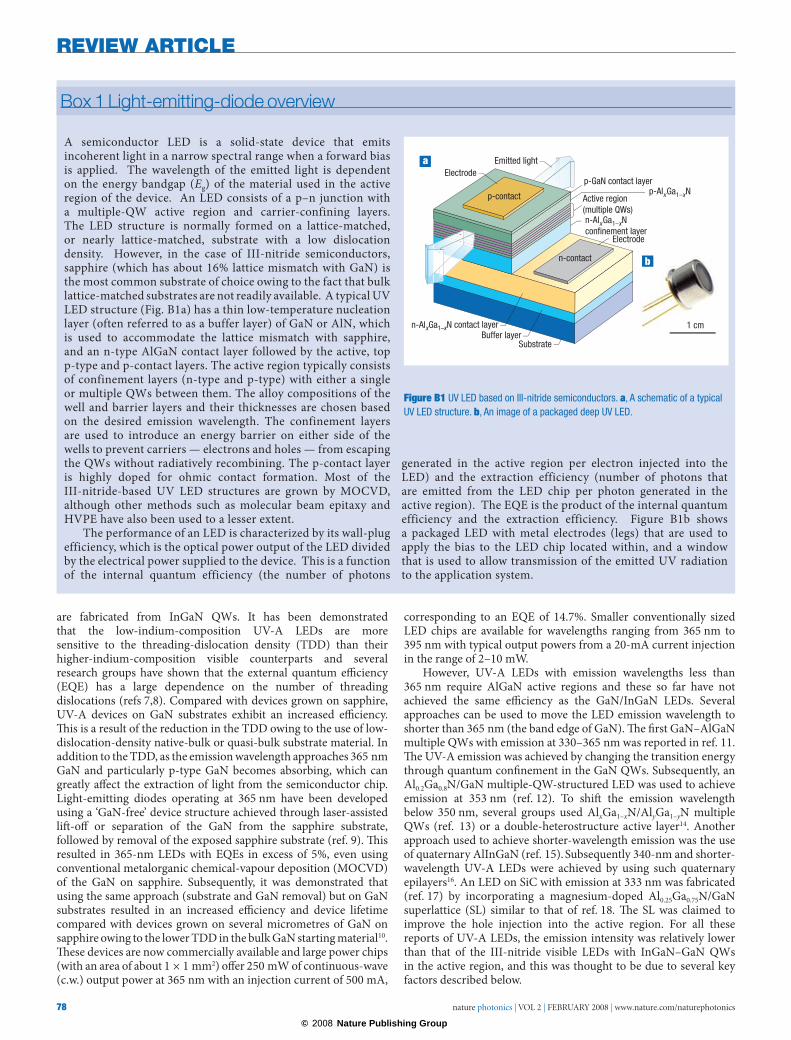
A semiconductor LED is a solid-state device that emits incoherent light in a narrow spectral range when a forward bias is applied. The wavelength of the emitted light is dependent on the energy bandgap (Eg) of the material used in the active region of the device. An LED consists of a p–n junction with a multiple-QW active region and carrier-confining layers. The LED structure is normally formed on a lattice-matched, or nearly lattice-matched, substrate with a low dislocation density. However, in the case of III-nitride semiconductors, sapphire (which has about 16% lattice mismatch with GaN) is the most common substrate of choice owing to the fact that bulk lattice-matched substrates are not readily available. A typical UV LED structure (Fig. B1a) has a thin low-temperature nucleation layer (often referred to as a buffer layer) of GaN or AlN, which is used to accommodate the lattice mismatch with sapphire, and an n-type AlGaN contact layer followed by the active, top p-type and p-contact layers. The active region typically consists of confinement layers (n-type and p-type) with either a single or multiple QWs between them. The alloy compositions of the well and barrier layers and their thicknesses are chosen based on the desired emission wavelength. The confinement layers are used to introduce an energy barrier on either side of the wells to prevent carriers — electrons and holes — from escaping the QWs without radiatively recombining. The p-contact layer is highly doped for ohmic contact formation. Most of the III-nitride-based UV LED structures are grown by MOCVD, although other methods such as molecular beam epitaxy and HVPE have also been used to a lesser extent.
The performance of an LED is characterized by its wall-plug efficiency, which is the optical power output of the LED divided by the electrical power supplied to the device. This is a function of the internal quantum efficiency (the number of photons
generated in the active region per electron injected into the LED) and the extraction efficiency (number of photons that are emitted from the LED chip per photon generated in the active region). The EQE is the product of the internal quantum efficiency and the extraction efficiency. Figure B1b shows a packaged LED with metal electrodes (legs) that are used to apply the bias to the LED chip located within, and a window that is used to allow transmission of the emitted UV radiation to the application system.
Box 1 Light-emitting-diode overview
1 cm
Emitted light
SubstrateBuffer layer
n-AlxGa1–xN contact layer
n-AlxGa1–xN confinement layer
Electrode
Electrode
n-contact
p-contact Active region (multiple QWs)
p-GaN contact layerp-AlxGa1–xN
Figure B1 uv led based on iii-nitride semiconductors. a, A schematic of a typical uv led structure. b, An image of a packaged deep uv led.
© 2008 Nature Publishing Group
REVIEW ARTICLE
nature photonics | VOL 2 | FEBRUARY 2008 | www.nature.com/naturephotonics 79
The quAnTum-confined sTArK effecT
The spontaneous and piezoelectric fields in the QWs composed of III-nitride materials are significantly stronger than other semiconductors, such as GaAs–AlGaAs. For III-nitride materials these fields get stronger as the aluminium content of the alloy compositions increases to achieve shorter-wavelength emission. These electric fields lead to a reduced radiative recombination efficiency in III-nitride materials owing to the quantum-confined Stark effect19,20. This effect bends the semiconductor valence and conduction bands leading to a physical separation of the electron and hole pairs. Thus their recombination probability in the QWs is reduced, which in turn leads to reduced emission efficiencies21.
ABsence of Alloy clusTeringIt was thought that the unusually high efficiency for visible emitters, given the relatively large TDD (more than 108 cm–2) in the active region, was due to the formation of indium-rich clusters that physically confined carriers in the InGaN–GaN quantum wells and separated them from threading dislocations. Absence of this alloy clustering in GaN and AlGaN QW UV-emitting devices is thought to cause their reduced radiative recombination efficiency. More recently, however, the indium-clustering hypothesis has been under question. Transverse-electromagnetic-field measurements have been performed on samples under various incident electron-beam dosages and showed a correlation between their measurement conditions and the observed ‘alloy clustering’22. In view of this evidence, continued exploration of recombination physics for both InGaN/GaN QWs, and their AlGaN/AlGaN UV counterparts is necessary to determine whether there are any
fundamental differences in the active regions of visible and UV LEDs and their respective recombination mechanisms.
low cArrier confinemenTEarly reports of UV LEDs commonly showed multiple emission peaks at long wavelengths, indicating a loss of carriers to regions other than the active region and hence unintended radiative transitions. At the time, it was unclear whether this was the result of deep-level transitions in the QWs, or from recombination occurring outside the active region. It was, however, observed that the addition of p-type AlGaN above the QWs reduced the intensity of the deep-level peaks, indicating that these peaks resulted from electrons passing through the active region and recombining with holes in the p-type material14. Confinement of electrons using a higher-aluminium-composition AlGaN electron-blocking layer between the QWs and the p-type contact layer was determined to be more effective than efforts to confine holes using a similar hole-blocking layer between the QWs and the n-AlGaN contact layer, owing to the low mobility and injection efficiency of the holes compared with electrons. Similar electron-blocking layers are commonly used for blue InGaN/GaN LEDs and laser diodes to avoid long-wavelength emission.
ABsorBing TemplATes And suBsTrATesAdditionally, in many of the LED structures discussed above, except the now commercially available devices used in refs 9 and 10, the devices were grown on either conducting SiC substrates or on thick GaN layers deposited over sapphire substrates. Both of these starting templates absorb UV radiation resulting in a low
AlN
AlxGaN/AlyGaN SL
PALE AlN150 Å
1 µm
2 µm
34.0 34.4 34.8 35.2 35.6 36.0 36.4 36.8 37.2100
101
102
103
104
105
SL+3
SL+2
SL+1
SL–5
SL–4
SL–3
SL–2
SL–1SL0
AlN
Inte
nsity
(a.u
.)
SL+3
2 (°)θ
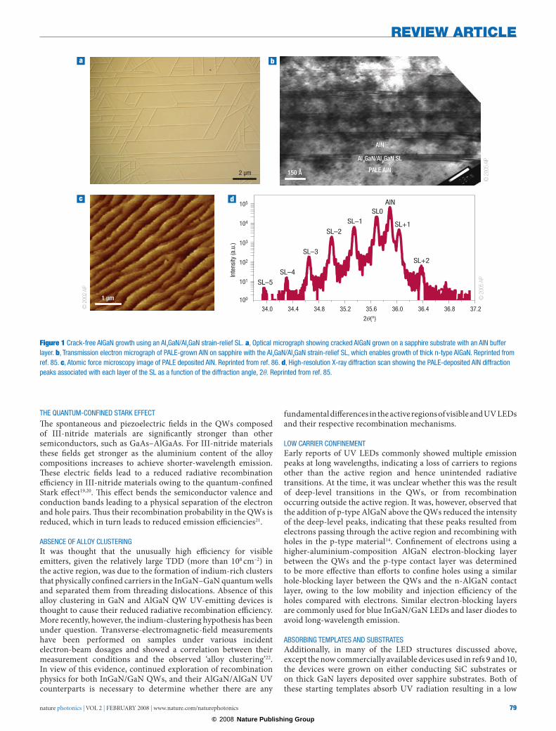
Figure 1 crack-free Algan growth using an Alxgan/Alygan strain-relief sl. a, optical micrograph showing cracked Algan grown on a sapphire substrate with an Aln buffer layer. b, Transmission electron micrograph of pAle-grown Aln on sapphire with the Alxgan/Alygan strain-relief sl, which enables growth of thick n-type Algan. reprinted from ref. 85. c, Atomic force microscopy image of pAle deposited Aln. reprinted from ref. 86. d, high-resolution X-ray diffraction scan showing the pAle-deposited Aln diffraction peaks associated with each layer of the sl as a function of the diffraction angle, 2θ. reprinted from ref. 85.
© 2
002
AIP
© 2
005
AIP
© 2
005
AIP
© 2008 Nature Publishing Group
REVIEW ARTICLE
80 nature photonics | VOL 2 | FEBRUARY 2008 | www.nature.com/naturephotonics
extraction efficiency from the semiconductor chip. In addition to absorbing materials beneath the QWs, the UV emission was primarily extracted through thin absorbing p-GaN contact layers and thin semitransparent metal contacts. Both p-type GaN and typical contact metals have strong UV absorption, even as thin films, and the absorption coefficient increases further with decreasing emission wavelength.
Although substrate absorption limited the extraction efficiency of early devices, several groups were able to demonstrate that defects in the material also contribute towards a decrease in the efficiency of these devices, and thus obtained reasonable output powers even for devices grown on absorbing substrates by minimizing defects. A 352-nm LED with an EQE of 1% was measured for a device grown on a free-standing GaN substrate, with a typical dislocation density of about 1 × 106 cm–2 (ref. 23). Light-emitting diodes grown on absorbing SiC operating at 340 nm with an EQE of 4% were also demonstrated. Here a broad-area defect-reduction growth technique was implemented, by which silicon nitride defect masks are deposited on the surface in a random orientation to block crystalline defects from propagating into the active region of the LED (ref. 24). This work demonstrated the potential for much higher-power UV emitters owing to the possibility of overcoming current limitations both with respect to the internal and extraction efficiency of the devices.
Despite the still relatively low quantum efficiency compared with visible LEDs, UV-A LEDs are starting to find applications in fluorescence spectroscopy and industrial curing25,26.
mid- And shorT-wAvelengTh emission
Shorter-wavelength UV-B and UV-C LEDs are of interest for several applications, primarily owing to the interaction between UV radiation in this wavelength regime and biological species. It must also be mentioned that the absorption of radiation by the atmospheric ozone is very strong for UV wavelengths shorter than about 280 nm, resulting in very little solar radiation in this wavelength regime being present near the Earth’s surface.
Low- and medium-pressure mercury lamps with an emission spectrum ranging from 254 nm to about 290 nm have been used extensively for purification of microbiological contaminants in air and water. These systems work primarily through a process by which adjacent thymine nucleic acids on DNA are dimerized, preventing replication of the microorganisms. This process has been shown to be effective, depending on the UV
dosage, for contaminants such as E. coli, giardia, and even more resistant virus strains such as adenovirus. Light-emitting diodes operating at 280 nm were the first to be developed, owing to the fluorescence interaction between biological agents of interest and this wavelength of light. Fluorescence-based biosensors were then developed to combat the threat of aerosolized biological weapons. Longer wavelength UV-B is of interest for medical applications, and this wavelength is already being used for treatment of skin disorders such as psoriasis.
The primary difference between UV-B or UV-C devices and the previously discussed UV-A is that it is not possible to use the GaN base layer commonly used with UV-A devices, owing to the much larger tensile strain that results for AlGaN grown on GaN. This leads to cracking of the AlGaN films and catastrophic failure of the LED. Increasing the aluminium composition (as is necessary for the UV-B and UV-C wavelengths) also leads to difficulties in the growth of material with high structural quality, typically resulting in an even higher dislocation density for AlGaN alloys compared with GaN. It also leads to difficulties in doping the material to impart n-type and p-type conductivity.
growTh of high-Aluminium AlloysTo fabricate efficient UV-B and UV-C LEDs, UV-transparent, low-defect-density AlN and AlGaN films are required. Compared with GaN, the growth of AlGaN, has proved to be significantly more difficult because aluminium adatoms have a much larger sticking coefficient and much lower surface mobility than gallium adatoms. It is well known that layer-by-layer growth of films, whereby adatoms bond at steps or kinks in the growth surface, results in smoother surface features than are obtained for three-dimensional island growth. Because aluminium adatoms have a low surface mobility, they are unable to move from their point of impact on the surface to energetically favourable lattice steps, resulting in three-dimensional island growth. As a result, a high density of extended defects, such as dislocations and grain boundaries, are generated as the growth islands from different nucleation sites coalesce. Although this phenomenon was observed for GaN, it was a much greater problem for AlN and AlGaN alloys with typical dislocation densities in the range of 1010–1011 cm–2 for AlN compared with about 108 cm–2 for GaN (ref. 27). Furthermore, in their growth by MOCVD, the commonly used aluminium-metalorganic precursors (trimethylaluminium and triethylaluminium) have been shown to react readily with the nitrogen gas source (NH3), resulting in gas-phase adduct formation that degrades the quality of the resulting AlN and AlGaN layers.
An alloy composition with a low group V to group III ratio (about 1:4 compared with several thousand) and high growth temperatures in excess of 1,200 °C were used to achieve a two-dimensional growth mode for AlN on sapphire28. It has also been suggested that a pulsed atomic-layer epitaxy (PALE) approach could be used to grow high-quality AlN and AlGaN films29. In PALE the flow rates of group III and group V precursors are sequentially modulated, thus enhancing surface migration of aluminium and gallium adatoms. This growth approach resulted in epitaxial layers with better crystalline quality and surface morphology. More recently, high-temperature growth has been investigated with growth temperatures up to 1,500 °C and AlN layers grown this way on 6H–SiC have been reported to be of high structural quality with a low dislocation density of the order of 106 cm–2 (ref. 30). Using these approaches, two-dimensional AlN films with UV transparency have been grown on sapphire with screw-type dislocation densities approaching 108 cm–2 and edge-type dislocation densities of about 1010 cm–2 (refs 31,32).
Given that most research groups have adopted the approach of starting with an AlN/sapphire template as the basis for the UV LED growth, a second challenge is managing the stress to allow
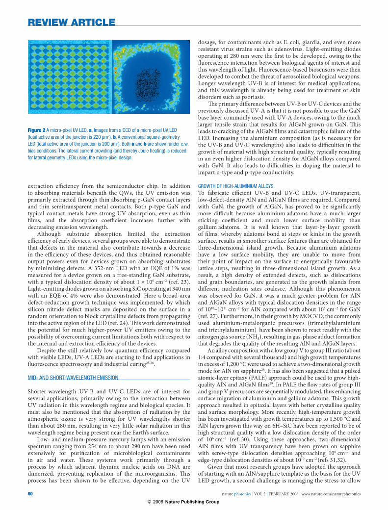
Figure 2 A micro-pixel uv led. a, images from a ccd of a micro-pixel uv led (total active area of the junction is 220 µm2). b, A conventional square-geometry led (total active area of the junction is 200 µm2). Both a and b are shown under c.w. bias conditions. The lateral current crowding (and thereby Joule heating) is reduced for lateral geometry leds using the micro-pixel design.
© 2008 Nature Publishing Group
REVIEW ARTICLE
nature photonics | VOL 2 | FEBRUARY 2008 | www.nature.com/naturephotonics 81
growth of thick, low-resistance n-type AlGaN for the laterally conducting n-contact layer. Interlayers of AlN and AlGaN have been grown at low temperatures to avoid cracking of AlGaN (refs 33,34). Periodic insertion of low-temperature-grown III-nitride layers was shown to effectively reduce the biaxial tensile strain in AlGaN films (this technique has been demonstrated for most III-nitride alloys), thus reducing the cracking35. An alternative approach was suggested in ref. 36, where the elastic strain relaxation in GaN/AlN and GaN/AlGaN SLs was theoretically predicted. The use of AlN/AlGaN SLs to alleviate the cracking of thick AlGaN films over sapphire substrates has also been reported37, and it has been noted from detailed X-ray measurements that these SLs were efficient in enhancing the AlGaN mosaic block dimensions38 (See Fig. 1). Development of the AlGaN/AlN SL buffer layers enabled growth of highly doped n-AlGaN to a thickness greater than 2.0 μm (ref. 37), enabling development of UV-B and UV-C LED devices first with submilliwatt- and later with milliwatt-level output powers. Submilliwatt operation at 315 nm and milliwatt operation at 325 nm were subsequently reported for LEDs with thick n-AlGaN layers that were flip-chip packaged to aid thermal dissipation39. Further optimization of the AlN-buffer-layer quality by means of PALE enabled improvements in the material quality of the n-AlGaN bottom-cladding layer, as well as the multiple QW layers, and resulted in the first milliwatt level UV-C LEDs (ref. 40). More improvements in the device design and packaging resulted in UV-C LEDs with EQEs exceeding 1% (ref. 13).
In addition to the challenges discussed concerning the growth of AlN/AlGaN with a high structural quality, as the aluminium composition is increased, the bandgap of the semiconductor increases and the ionization energies for silicon (n-type dopant) and magnesium (p-type dopant) increase, resulting in a lower ionization efficiency. Therefore both n-type and p-type doping of AlGaN films with high aluminium concentrations is much more difficult than GaN. Low-resistivity films are specifically desired because most deep-UV LEDs are prepared on transparent sapphire, with a few initial demonstrations using bulk AlN substrates. Both of these substrate materials are electrically insulating, requiring fabrication of laterally conducting LEDs with both contacts on the same side of the wafer. Higher resistivity of the n-contact AlGaN layer, results in non-uniform current injection in the
diode active area, known as ‘current crowding’. Current crowding leads to increased injection currents along the perimeter of the LED mesa41. As the ionization energy for magnesium dopants in p-type GaN is already relatively high at 250 meV, p-type doping of high-aluminium-content AlGaN is even more challenging. It increases for AlGaN such that it is difficult to achieve conduction in p-type AlGaN with an aluminium composition greater than about 15–20%. In addition to increasing the device resistance, which results in Joule heating, it is very difficult to make an ohmic contact to p-AlGaN films. Therefore, most researchers deposit a p-GaN film to the top surface to serve as a contact layer, with this film absorbing some of the UV emission. Even if holes can be effectively injected from the metal into the p-GaN material, such holes are then faced with a potential barrier before they can be transported across subsequent AlGaN barrier layers down to the QWs. Holes that are trapped at the first interface set up an electric field, which can attract electrons to bypass the QWs and hence recombine non-radiatively in the p-GaN layer, and this has a major impact on the quantum efficiency.
lATerAl currenT crowdingThe problem of lateral current crowding with electrically insulating substrates, and more particularly sapphire-based deep-UV LEDs has been analysed, and an interdigitated multi-finger geometry was demonstrated40,42. Using this electrode geometry, the lateral distance between adjacent n-contact metallization is reduced, leading to more spatially uniform current injection throughout the active region of the device. This enables larger active areas than those of square- or circular-geometry LEDs. To improve the current spreading in LEDs with high aluminium molar fractions in the AlGaN cladding layers, an interconnected micropixel design has also been adapted40,43. The use of micropixels was first introduced for III-nitrides44 to improve the light extraction from an AlGaN/GaN slab through the formation of microcavities, and the approach was then used in blue45 and UV-A LEDs (ref. 46). The micropixel LED design was further extended to the formation of photonic crystals47 by reduction of the size and period of the array elements48,49. An LED design with interconnected micropixels separated by the n-AlGaN contact metal was also shown to be very efficient in achieving the desired uniform current pumping for deep-UV-C
00
20
20
40
40
60
60
80
80
100
100
c.w
. pow
er (a
.u.)
Flip-chip
On-wafer
Current (mA)
p+-GaN
Gold supports
Mount/header
Gold supportsp-AlGaN
AlGaN multiple QW
n+-AlGaNbarrier
AIN/AlGaN SL
PALEAlN bufferlayer
Sapphire
Ti/Al/Ti/Au
AlN carrier
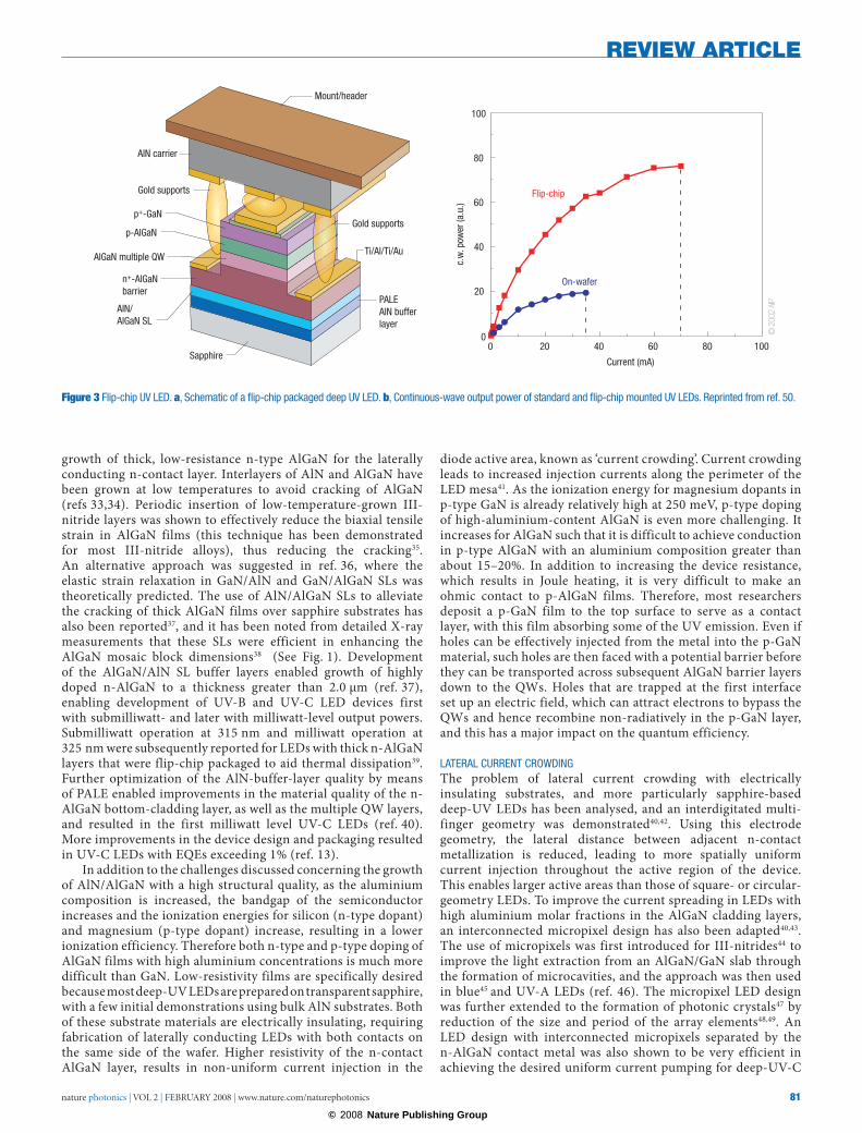
Figure 3 flip-chip uv led. a, schematic of a flip-chip packaged deep uv led. b, continuous-wave output power of standard and flip-chip mounted uv leds. reprinted from ref. 50.
© 2
002
AIP
© 2008 Nature Publishing Group
REVIEW ARTICLE
82 nature photonics | VOL 2 | FEBRUARY 2008 | www.nature.com/naturephotonics
LEDs. Devices that emit at 255 nm with output powers of 1 mW c.w. and 3.4 mW pulsed and corresponding maximum quantum efficiencies of 0.14% and 0.3% (for c.w. and pulsed pumping, respectively) were demonstrated with this design40. Figure 2 shows images obtained from a CCD camera with conventional geometry and micropixel-designed UV LEDs during c.w. operation. Changes in the colour indicate non-uniform emission due to spatial variations in current injection.
efficienT ThermAl mAnAgemenTUnder typical c.w. operation, most of the sapphire-based deep-UV LEDs suffer from excessive self-heating owing to the relatively higher operating voltages (which result in eddy current losses), low emission efficiencies and poor thermal conductivity of the sapphire (0.35 W cm–1 K–1). This severe self heating leads to a reduction of the device lifetime and a spectral shift in the emission. Flip-chip packaging has been used to mitigate device self heating50. In this method, the LED chip is cut out separately and mounted in a flip-chip configuration with a high thermal conductivity 175 W mK–1 insulating AlN carrier with thermocompression gold bonding. The AlN carrier and flip-chip UV LED are then mounted on a gold-coated header (see Fig. 3a). Figure 3b presents the c.w. optical power as a function of pump current for the standard and the flip-chip packaged LEDs. As can be seen from the graph, the performance of the device is improved by the flip-chip packaging technique. The saturation current (which is indicative of device self heating) was increased using the flip-chip package thereby enabling higher output power with higher input drive currents. The slope of the curve also improved owing to better light extraction after flip-chip packaging.
fuTure ouTlooK
Impressive research efforts in the development of III-nitride UV devices (see Table 1) have resulted in operation over a wide range of UV wavelengths from 210–400 nm. Despite the material and
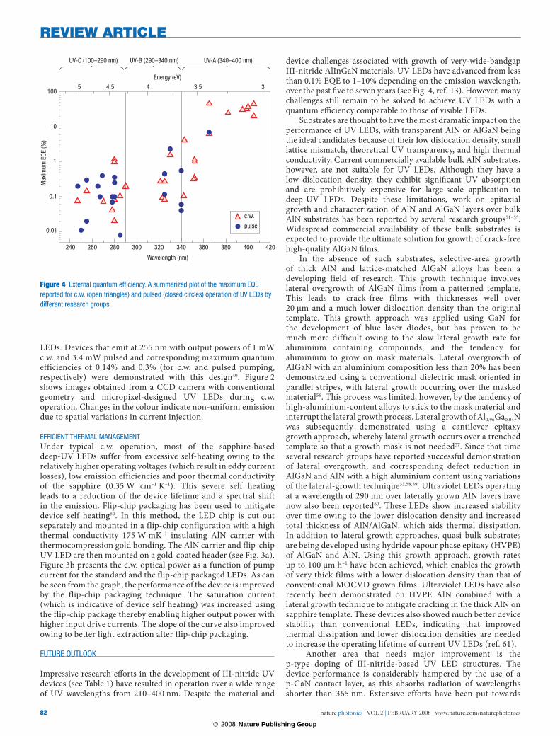
device challenges associated with growth of very-wide-bandgap III-nitride AlInGaN materials, UV LEDs have advanced from less than 0.1% EQE to 1–10% depending on the emission wavelength, over the past five to seven years (see Fig. 4, ref. 13). However, many challenges still remain to be solved to achieve UV LEDs with a quantum efficiency comparable to those of visible LEDs.
Substrates are thought to have the most dramatic impact on the performance of UV LEDs, with transparent AlN or AlGaN being the ideal candidates because of their low dislocation density, small lattice mismatch, theoretical UV transparency, and high thermal conductivity. Current commercially available bulk AlN substrates, however, are not suitable for UV LEDs. Although they have a low dislocation density, they exhibit significant UV absorption and are prohibitively expensive for large-scale application to deep-UV LEDs. Despite these limitations, work on epitaxial growth and characterization of AlN and AlGaN layers over bulk AlN substrates has been reported by several research groups51–55. Widespread commercial availability of these bulk substrates is expected to provide the ultimate solution for growth of crack-free high-quality AlGaN films.
In the absence of such substrates, selective-area growth of thick AlN and lattice-matched AlGaN alloys has been a developing field of research. This growth technique involves lateral overgrowth of AlGaN films from a patterned template. This leads to crack-free films with thicknesses well over 20 μm and a much lower dislocation density than the original template. This growth approach was applied using GaN for the development of blue laser diodes, but has proven to be much more difficult owing to the slow lateral growth rate for aluminium containing compounds, and the tendency for aluminium to grow on mask materials. Lateral overgrowth of AlGaN with an aluminium composition less than 20% has been demonstrated using a conventional dielectric mask oriented in parallel stripes, with lateral growth occurring over the masked material56. This process was limited, however, by the tendency of high-aluminium-content alloys to stick to the mask material and interrupt the lateral growth process. Lateral growth of Al0.96Ga0.04N was subsequently demonstrated using a cantilever epitaxy growth approach, whereby lateral growth occurs over a trenched template so that a growth mask is not needed57. Since that time several research groups have reported successful demonstration of lateral overgrowth, and corresponding defect reduction in AlGaN and AlN with a high aluminium content using variations of the lateral-growth technique33,58,59. Ultraviolet LEDs operating at a wavelength of 290 nm over laterally grown AlN layers have now also been reported60. These LEDs show increased stability over time owing to the lower dislocation density and increased total thickness of AlN/AlGaN, which aids thermal dissipation. In addition to lateral growth approaches, quasi-bulk substrates are being developed using hydride vapour phase epitaxy (HVPE) of AlGaN and AlN. Using this growth approach, growth rates up to 100 μm h–1 have been achieved, which enables the growth of very thick films with a lower dislocation density than that of conventional MOCVD grown films. Ultraviolet LEDs have also recently been demonstrated on HVPE AlN combined with a lateral growth technique to mitigate cracking in the thick AlN on sapphire template. These devices also showed much better device stability than conventional LEDs, indicating that improved thermal dissipation and lower dislocation densities are needed to increase the operating lifetime of current UV LEDs (ref. 61).
Another area that needs major improvement is the p-type doping of III-nitride-based UV LED structures. The device performance is considerably hampered by the use of a p-GaN contact layer, as this absorbs radiation of wavelengths shorter than 365 nm. Extensive efforts have been put towards
0.1
0.01
1
10
100
Max
imum
EQE
(%)
Wavelength (nm)
c.w.
pulse
UV-C (100–290 nm) UV-B (290–340 nm) UV-A (340–400 nm)
5 4.5 4 3.5 3
420400380360340320300280260240
Energy (eV)
Figure 4 external quantum efficiency. A summarized plot of the maximum eqe reported for c.w. (open triangles) and pulsed (closed circles) operation of uv leds by different research groups.
© 2008 Nature Publishing Group
REVIEW ARTICLE
nature photonics | VOL 2 | FEBRUARY 2008 | www.nature.com/naturephotonics 83
improvement of p-type doping in AlxGa1–xN materials and to find a viable alternative material for the contact layer40. Use of short- or long-period superlattices (SPSLs or LPSLs) comprising magnesium-doped AlGaN/GaN layers has been attempted to replace conventional p-AlGaN. By using an SPSL, vertical p-conduction is improved owing to the formation of minibands, and with an LPSL good horizontal p-conductivity has been reported. A magnesium-doped AlGaN/GaN SPSL has been effectively grown to fabricate an LED operating at wavelengths of 340–350 nm (ref. 62). Another notable method to obtain better hole conduction was Mg δ-doping — the growth of abrupt, shallow and narrow doping profiles in a semiconductor63. This approach has been reported to enhance the hole concentration while inducing no changes in the hole mobility. A single heterostructure of p-GaN/p-AlGaN has also been used to achieve hole accumulation at the interface64. The accumulation of holes at the interface enhances the vertical conductivity as a result of field-assisted tunnelling and thermionic emission, as only one barrier exists for hole transport.
Additionally, all UV LED development so far has been performed on the hexagonal wurtzite {0001} plane, resulting in growth along the polar axis. As mentioned previously, this leads to the quantum-confined Stark effect and reduces the recombination efficiency of LEDs. This could be overcome by performing growth along non-polar orientations, such as, <101̄0> and <112̄0>, and to a lesser extent by using semipolar orientations, such as <101̄1>. The feasibility of growth over non-polar substrates, such as, r-plane sapphire has now been demonstrated65. In the past, there have been extensive analyses of the device-oriented growth of non-polar materials using non-polar sapphire substrates and GaN templates through approaches, such as selective-area lateral epitaxy66. Based on the high-quality non-polar epitaxial layers, stimulated emission at short wavelengths of 353 nm (ref. 67), LEDs emitting in the visible spectrum68 and photodetectors69 were reported with either a reduced or no quantum-confined Stark effect. However, the efficiencies of these devices were plagued by a high number of defects owing to the lack of bulk substrates. Recently, there have been demonstrations of LEDs and laser diodes grown on non-polar m-plane GaN bulk substrates with a performance beginning to approach that of the more mature polar devices70–72.
Based on these developments, it is expected that this work will be continued into the deep-UV region with an increase in radiative recombination efficiency expected.
doi:10.1038/nphoton.2007.293
references1. Morkoc, H. Handbook of Nitride Semiconductors and Devices Vol. 1(Springer, 2007).2. Amano, H., Sawaki, N., Akasaki, I. & Toyoda, Y. Metalorganic vapor phase epitaxial growth of a
high quality GaN film using an AlN buffer layer. Appl. Phys. Lett. 48, 353–355 (1986).3. Nakamura, S. GaN growth using GaN buffer layer. Jpn J. Appl. Phys. 30, L1705–L1707 (1991).4. Amano, H., Kito, M., Hiramatsu, K. & Akasaki, I. P-type conduction in Mg-doped GaN treated
with low-energy electron beam irradiation (LEEBI). Jpn J. Appl. Phys. 28, L2112–L2114 (1989).5. Nakamura, S., Mukai, T., Senoh, M. & Iwasa, N. Thermal annealing effects on p-type Mg-doped
GaN films. Jpn J. Appl. Phys. 31, L139–L142 (1992).6. Razeghi, M. & Henini, M. Optoelectronic devices: III-nitrides 1–9 (Elsevier, Oxford, 2004).7. Mukai, T., Nagahama, S., Iwasa, N., Senoh, M. & Yamada, T. Nitride light-emitting diodes.
J. Phys.: Condens. Matter 13, 7089–7098 (2001).8. Akita, K., Kyono, T., Yoshizumi, Y., Kitabayashi, H. & Katayama, K. Characteristics of InGaN light-
emitting diodes on GaN substrates with low threading dislocation densities. Phys. Status Solidi a 204, 246–250 (2007).
9. Morita, D. et al. High output power 365 nm ultraviolet light emitting diode of GaN-free structure. Jpn J. Appl. Phys. 41, L1434-L1436 (2002).
10. Mukai, T. et al. Investigation of optical-output-power degradation in 365-nm UV-LEDs. Phys. Status Solidi c 3, 2211–2214 (2005).
11. Khan, M. A., Skogman, R. A., Van Hove, G. M., Krishnankutty, S. & Kolbas, R. M. Photoluminescence characteristics of AlGaN-GaN-AlGaN quantum wells. Appl. Phys. Lett. 56, 1257–1259 (1990).
12. Han, J. et al. AlGaN/GaN quantum well ultraviolet light emitting diodes. Appl. Phys. Lett. 73, 1688–1690 (1998).
13. Nishida, T. & Kobayashi, N. 346 nm emission from AlGaN multi-quantum-well light emitting diode. Phys. Status Solidi a 176, 45–48 (1999).
14. Otsuka, N. et al. Room temperature 339 nm emission from Al0.13Ga0.87N/ Al0.10Ga0.90N double heterostructure light-emitting diode on sapphire substrate. Jpn J. Appl. Phys. 39, L445–L448 (2000).
15. Khan, M. A. et al. Lattice and energy band engineering in AlInGaN/GaN heterostructures. Appl. Phys. Lett. 76, 1161–1163 (2000).
16. Khan, M. A. et al. Stripe geometry ultraviolet light emitting diodes at 305 nanometers using quaternary AlInGaN multiple quantum wells. Jpn J. Appl. Phys. 40, L1308–L1310 (2001).
17. Kinoshita, A., Hirayama, H., Ainoya, M., Aoyagi, Y. & Hirata, A. Room-temperature operation at 333 nm of Al0.03Ga0.97N/Al0.25Ga0.75N quantum-well light-emitting diodes with Mg-doped superlattice layers. Appl. Phys. Lett. 77, 175–177 (2000).
18. Nishida, T., Saito, H., Kumakura, K., Makimoto, T. & Kobayashi, H. Proceedings of International Workshop on Nitride Semiconductors (IWN 2000), IPAP Conference Series 1 725–727 (2000).
19. Lefebvre, P. et al. Quantum-confined Stark effect and recombination dynamics of spatially indirect excitons in MBE-grown GaN-AlGaN quantum wells. MRS Int. J. Nitrogen Semiconductor Res. 4S1, G3.69 (1999).
20. Waltereit, P. et al. Nitride semiconductors free of electrostatic fields for efficient white light-emitting diodes. Nature 406, 865–868 (2000).
21. Bernardini, F., Fiorentini, V. & Vanderbilt, D. Spontaneous polarization and piezoelectric constants of III-V nitrides. Phys. Rev. B. 56, R10024–R10027 (1997).
22. Smeeton, T. M., Humphreys, C. J., Barnard, J. S. & Kappers, M. J. The impact of electron beam damage on the detection of indium-rich localization centres in InGaN quantum wells using transmission electron microscopy. J. Mater. Sci. 41, 2729–2737 (2006).
23. Motoki, K. et al. Preparation of large freestanding GaN substrates by hydride vapor phase epitaxy using GaAs as a starting substrate. Jpn J. Appl. Phys. 40, L140–L143 (2001).
24. Edmond, J. et al. High efficiency GaN-based LEDs and lasers on SiC. J. Crystal Growth 272, 242–250 (2004).
25. Jeon, S. R. et al. High performance AlGaInN ultraviolet light-emitting diode at the 340 nm wavelength. Jpn J. Appl. Phys. 43, L1409–L1412 (2004).
26. Jeys, T. H., Desmarais, L., Lynch, E. J. & Ochoa, J. R. Development of a UV-LED-based biosensor Proc. SPIE 5071, 234–240 (2003).
27. Imura, M. et al. Dislocations in AlN epilayers grown on sapphire substrate by high-temperature metal-organic vapor phase epitaxy. Jpn J. Appl. Phys. 46, 1458–1462 (2007).
28. Ohba, Y. & Sato, R. Growth of AlN on sapphire substrates by using a thin AlN buffer layer grown two-dimensionally at a very low V/III ratio. J. Crystal Growth. 221, 258–261 (2000).
29. Khan, M. A., Kuzina, J. N., Olson, D. T., George, T. & Pike, W. T. GaN/AlN digital alloy short-period superlattices by switched atomic layer metalorganic chemical vapor deposition. Appl. Phys. Lett. 63, 3470–3472 (1993).
30. Balakrishnan, K. et al. Influence of high temperature in the growth of low dislocation content AlN bridge layers on patterned 6H-SiC substrates by metalorganic vapor phase epitaxy. Jpn J. Appl. Phys. 46, L307–L310 (2007).
31. Chen, Z. et al. Pulsed lateral epitaxial overgrowth of aluminum nitride on sapphire substrates. Appl. Phys. Lett. 89, 081905 (2006).
32. Imura, M. et al. Microstructure of epitaxial lateral overgrown AlN on trench-patterned AlN template by high-temperature metal-organic vapor phase epitaxy. Appl. Phys. Lett. 89, 221901 (2006).
33. Kamiyama, S. et al. Low-temperature-deposited AlGaN interlayer for improvement of AlGaN/GaN heterostructure. J. Crystal Growth 223, 83–91 (2001).
34. Han, J. et al. Control and elimination of cracking of AlGaN using low-temperature AlGaN interlayers. Appl. Phys. Lett. 78, 67–69 (2001).
35. Jain, S. C., Willander, M., Narayan, J. & Overstraeten, R. III–nitrides: growth, characterization, and properties. J. Appl. Phys. 87, 965–1006 (2000).
36. Bykhovski, A. D., Gelmont, B. L. & Shur, M. S. Elastic strain relaxation and piezoeffect in GaN-AlN, GaN-AlGaN and GaN-InGaN superlattices. J. Appl. Phys. 81, 6332–6338 (1997).
Table 1 Brief summary of some of the key developments and milestones achieved during the development of UV LEDs.
Key developments group, year
low-temperature Aln buffer layer Amano et al. 1986 (ref. 2)p-type gan by low-energy electron beam irradiation
Amano et al. 1989 (ref. 4)
first Algan-gan-Algan multiple-qw Khan et al. 1990 (ref. 11)low-temperature gan buffer layer nakamura et al. 1991 (ref. 73)first Algan/gan multiple-qw led (353 nm) han et al. 1998 (ref. 12)smooth Aln with low v/iii ratio ohba et al. 1996, 2001 (refs 74,75)first 352-nm led on bulk gan nishida et al. 2001 (ref. 76)first 340-nm uv-A led Adivarahan et al. 2001 (ref. 77)first 315-nm led Khan et al. 2001 (ref. 16)first uv-B led (305 nm) Khan et al. 2001 (ref. 16)Aln/Algan sl for thick n-type Algan Zhang et al. 2002 (ref. 37)first uv-c led (285 nm) Adivarahan et al. 2002 (ref. 78)first gan-free uv led (365 nm) morita et al. 2002 (ref. 9)first 280-nm led yasan et al. 2002 (ref. 79)first 269-nm led Adivarahan et al. 2004 (ref. 80)first 254-nm led wu et al. 2004 (ref. 81)first 250-nm led Adivarahan et al. 2004 (ref. 82)first 210-nm Aln led Taniyasu et al. 2006 (ref. 83)stimulated emission from Aln at 214 nm shatalov et al. 2006 (ref. 84)
© 2008 Nature Publishing Group
REVIEW ARTICLE
84 nature photonics | VOL 2 | FEBRUARY 2008 | www.nature.com/naturephotonics
37. Zhang, J. P. et al. Crack-free thick AlGaN grown on sapphire using AlN/AlGaN superlattices for strain management. Appl. Phys. Lett. 80, 3542–3544 (2002).
38. Wang, H. M. et al. AlN/AlGaN superlattices as dislocation filter for low-threading-dislocation thick AlGaN layers on sapphire. Appl. Phys. Lett. 81, 604–606 (2002).
39. Chitnis, A. et al. Submilliwatt operation of AlInGaN based multifinger-design 315 nm light emitting diode (LED) over sapphire substrate. Jpn J. Appl. Phys. 41, L320–L322 (2002).
40. Khan, M. A., Shatalov, M., Maruska, H. P., Wang, H. M. & Kuokstis, E. III–nitride UV devices. Jpn J. Appl. Phys. 44, 7191–7206 (2005).
41. Guo, X. & Schubert, E. F. Current crowding and optical saturation effects in GaInN/GaN light-emitting diodes grown on insulating substrates. Appl. Phys. Lett. 78, 3337–3339 (2001).
42. Guo, X. & Schubert, E. F. Current crowding in GaN/InGaN light emitting diodes on insulating substrates. J. Appl. Phys. 90, 4191–4195 (2001).
43. Adivarahan, V. et al. High-power deep ultraviolet light-emitting diodes based on a micro-pixel design. Appl. Phys. Lett. 85, 1838–1840 (2004).
44. Mair, R. A. et al. Optical properties of GaN/AlGaN multiple quantum well microdisks. Appl. Phys. Lett. 71, 2898–2900 (1997).
45. Jin, S. X., Li, J., Li, J. Z., Lin, J. Y. & Jiang, H. X. GaN microdisk light emitting diodes. Appl. Phys. Lett. 76, 631–633 (2000).
46. Jeon, C. W., Gu. E. & Dawson, M. D. Mask-free photolithographic exposure using a matrix-addressable micropixellated AlInGaN ultraviolet light-emitting diode. Appl. Phys. Lett. 86, 221105 (2005).
47. Boroditsky, M. et al. Light extraction from optically pumped light-emitting diode by thin-slab photonic crystals. Appl. Phys. Lett. 75, 1036–1038 (1999).
48. Oder, T. N., Shakya, J., Lin, J. Y. & Jiang, H. X. III-nitride photonic crystals. Appl. Phys. Lett. 83, 1231–1233 (2003).
49 Oder, T. N., Kim, K. H., Lin, J. Y. & Jiang, H. X. III-nitride blue and ultraviolet photonic crystal light emitting diodes. Appl. Phys. Lett. 84, 466–468 (2004).
50. Chitnis, A. et al. Self-heating effects at high pump currents in deep ultraviolet light-emitting diodes at 324 nm. Appl. Phys. Lett. 81, 3491–3493 (2002).
51. Gaska, R. et al. Deep-ultraviolet emission of AlGaN/AlN quantum wells on bulk AlN. Appl. Phys. Lett. 81, 4658–4660 (2002).
52. Rojo, J. C. et al. Growth and characterization of epitaxial layers on aluminum nitride substrates prepared from bulk, single crystals. J. Crystal Growth 240, 508–512 (2002).
53. Hu, X. et al. AlGaN/GaN heterostructure field-effect transistors on single-crystal bulk AlN. Appl. Phys. Lett. 82, 1299–1301 (2003).
54. Nishida, T., Makimoto, T., Saito, H. & Ban, T. AlGaN-based ultraviolet light-emitting diodes grown on bulk AlN substrates. Appl. Phys. Lett. 84, 1002–1004 (2004).
55. Silveira, E. et al. Near-bandedge cathodoluminescence of an AlN homoepitaxial film. Appl. Phys.Lett. 84, 3501–3503 (2004).
56. Nam, O. H., Bremser, M. D., Ward, B. L., Nemanich, R. J. & Davis, R. F. Growth of GaN and Al0.2Ga0.8N on patterened substrates via organometallic vapor phase epitaxy. Jpn J. Appl. Phys. 36, L532–L535 (1997).
57 Katona, T. M. et al. Maskless lateral epitaxial overgrowth of high-aluminum-content AlxGa1–xN. Appl. Phys. Lett, 84, 5025–5027 (2004).
58. Wang, T., Bai, J., Parbrook, P. J. & Cullis, A. G. Air-bridged lateral growth of an Al0.98Ga0.02N layer by introduction of porosity in an AlN buffer. Appl. Phys. Lett. 87, 151906 (2005).
59. Imura, M. et al. Epitaxial lateral overgrowth of AlN on trench-patterned AlN layers. J. Crystal Growth 298, 257–260 (2007).
60. Adivarahan, V. et al. Robust 290 nm emission light emitting diodes over pulsed laterally overgrown AlN. Jpn J. Appl. Phys. 46, L877–L879 (2007).
61. Adivarahan, V. et al. Robust 285 nm deep UV light emitting diodes over metal organic hydride vapor phase epitaxially grown AlN/sapphire templates. Jpn J. Appl. Phys. 46, L537–L539 (2007).
62. Kozodoy, P., Hansen, M., DenBaars, S. P. & Mishra, U. K. Enhanced Mg doping efficiency in Al0.2Ga0.8N/GaN superlattices. Appl. Phys. Lett. 74, 3681–3684 (1999).
63. Nakarmi, M. L., Kim, K. H., Li, J., Lin, J. Y. & Jiang, H. X. Enhanced p-type conduction in GaN and AlGaN by Mg-δ-doping. Appl. Phys. Lett. 82, 3041–3043 (2003).
64. Shur, M. S. et al. Accumulation hole layer in p-GaN/AlGaN heterostructures. Appl. Phys. Lett. 76, 3061–3063 (2000).
65. Craven, M. D., Lim, S. H., Wu, F., Speck, J. & DenBaars, S. P. Threading dislocation reduction via laterally overgrown nonpolar (112̄0) a-plane GaN. Appl. Phys. Lett. 81, 1201–1203 (2002).
66. Chen, C. et. al. A new selective area lateral epitaxy approach for depositing a-plane GaN over r-plane sapphire. Jpn J. Appl. Phys. 42, L818-L820 (2003).
67. Chen, C. et al. Optically pumped lasing at 353 nm using non-polar a-plane AlGaN multiple quantum wells over r-plane sapphire. Jpn J. Appl. Phys. 43, L1099–L1102 (2004).
68. Chen, C. et al. Ultraviolet light emitting diodes using non-polar a-plane GaN-AlGaN multiple quantum wells. Jpn J. Appl. Phys. 42, L1039–L1040 (2003).
69. Adivarahan, V. et al. Planar Schottky diodes on high quality A-plane GaN. Jpn J. Appl. Phys. 42, L1136–L1138 (2003).
70. Schmidt, M. et al. High power and high external efficiency m-plane InGaN light emitting diodes. Jpn J. Appl. Phys. 46, L126–L128 (2007).
71. Feezell, D. F., DenBaars, S. P. & Nakamura, S. AlGaN-cladding-free nonpolar InGaN/GaN laser diodes. Jpn J. Appl. Phy. 46, L284–L286 (2007).
72. Okamoto, K. et al. Continuous-wave operation of m-plane InGaN multiple quantum well laser diodes. Jpn J. Appl. Phys. 46, L187–L189 (2007).
73. Nakamura, S., Harada, Y. & Seno, M. Novel metalorganic chemical vapor deposition system for GaN growth. Appl. Phys. Lett. 58, 2021–2023 (1991).
74. Ohba, Y. & Hatana, A. Growth of high-quality AlN and AlN/GaN/AlN heterostructure on sapphire substrate. Jpn J. Appl. Phys. 35, L1013–L1015 (1996).
75. Ohba, Y., Sato, R. & Kaneko, K. Two-dimensional growth of AlN and GaN on lattice-relaxed Al0.4Ga0.6N buffer layers prepared with high-temperature-grown AlN buffer on sapphire substrates and fabrication of multiple-quantum-well structures. Jpn J. Appl. Phys. 40, L1293–L1296 (2001).
76. Nishida, T., Saito, H. & Kobayashi, N. Efficient and high-power AlGaN-based ultraviolet light-emitting diode grown on bulk GaN. Appl. Phys. Lett. 79, 711–712 (2001).
77. Adivarahan, V. et al. Ultraviolet light-emitting diodes at 340 nm using quaternary AlInGaN multiple quantum wells. Appl. Phys. Lett. 79, 4240–4242 (2001).
78. Adivarahan, V. et al. AlGaN single-quantum-well light-emitting diodes with emission at 285 nm. Appl. Phys. Lett. 81, 3666–3668 (2002).
79. Yasan, A. et al. Top-emission ultraviolet light-emitting diodes with peak emission at 280 nm. Appl. Phys. Lett. 81, 801–802 (2002).
80. Adivarahan, V. et al. High-efficiency 269 nm emission deep ultraviolet light-emitting diodes. Appl. Phys. Lett. 84, 4762–4764 (2004).
81. Wu, S. et al. Micro-pixel design milliwatt power 254 nm emission light emitting diodes. Jpn J. Appl. Phys. 43, L1035–L1037 (2004).
82. Adivarahan, V. et al. 250 nm AlGaN light-emitting diodes. Appl. Phys. Lett. 85, 2175–2177 (2004).
83. Taniyasu, Y., Kasu, M. & and Makimoto, T. An aluminium nitride light-emitting diode with a wavelength of 210 nanometres. Nature 441, 325–328 (2006).
84. Shatalov, M., Gaevski, M., Adivarahan, V. & Khan, A. Room-temperature stimulated emission from AlN at 214 nm. Jpn J. Appl. Phys. 45, L1286–L1288 (2006).
85. Sun, W. H. et al. Fine structure of AlN/AlGaN superlattice grown by pulsed atomic-layer epitaxy for dislocation filtering. Appl. Phys. Lett. 87, 211915 (2005).
86. Zhang, J. P. Pulsed atomic-layer epitaxy of ultrahigh-quality AlxGa1–xN structures for deep ultraviolet emissions below 230 nm. Appl. Phys. Lett. 81, 4392–4394 (2002).
© 2008 Nature Publishing Group
Related Documents