1 SCIENTIFIC REPORTS | (2019) 9:14978 | https://doi.org/10.1038/s41598-019-51169-x www.nature.com/scientificreports Ultraviolet and Infrared luminescent Au-rich nanostructure growth in SiO 2 by burrowing and inverse Oswald ripening process D. P. Datta 1,2 , A. Chettah 3 , Arpan Maiti 4 , B. Satpati 4 & P. K. Sahoo 1* We study the evolution of nanoparticle morphology through successive stages when Au-Si bilayer on SiO 2 is irradiated with 500 keV Xe-ions and resulting luminescence in the UV, Visible and infrared range. An array of nanoscale island morphology is developed on the silica surface in the initial stage of evolution which undergoes gradual burrowing in the silica matrix accompanied by elongation of large ones in the direction of incident ions under cumulative ion irradiation. Burrowing is found to occur in order to minimize the surface free energy of the nanoparticles. Numerical simulation based on the unified thermal spike model shows formation of molten latent tracks due to ions energy release which drive the dewetting of the metal layer and further give mobility to nanoparticle atoms leading to burrowing in the later stage of evolution and elongation of large nanoparticles. Satellite nanoparticles are observed to grow around Au nanoparticles embedded in silica through nucleation of Au atoms dissolved in the matrix by incident ions. The varying diameters of the Au satellite nanoparticles seem to result in luminescence in the UV and infrared range. The observed structure may find application in surface enhanced Raman scattering, catalysis, and LEDs. Unique properties of nanoscale structures of metals, semiconductors, or their composites, originating from large surface to volume ratio, charge confinement in low dimension, etc., make them key components in present and future applications of nanotechnology 1–8 . Promising progress in plasmonics, photonics, optoelectronics, catalysis, sensors, or bioscience have been achieved through characteristic properties of nanoparticles, for instance, surface Plasmon resonance (SPR), i.e. strong absorbance of radiation at particular wavelength due to collective oscillation of conduction electrons in metal nanoparticles or enhanced electric field in the vicinity of a metal nanoparticles 5,7 . In the contexts of research on application of nanoparticles, Au nanoparticles receive particular attention for their potential applications. Catalytic activity of Au nanoparticles is utilized for growth of nanowires and nanotubes 9–11 . SPR and local field enhancement of Au nanoparticles are highly promising for surface enhanced Raman scat- tering (SERS) 12,13 plasmonic waveguides, photocatalysis, or biosensing 14–17 . Studies of nanoscale behaviour also indicate that the functionalities of nanoparticles can be significantly enhanced in case of metal-semiconductor nanocomposites 5–8 . A nanoscale composite of Au with any semiconductor material, therefore, holds highly promising possibility towards further improved physical and chemical properties. is fact motivated significant research effort towards synthesis of varied types of composite nanostructures with an emphasis on controllability of their shape and size, as well as exploration of their novel properties. Among the physiochemical techniques for synthesis of nanoscale structures, dewetting of a metal film by irradiation of energetic ion beam has offered single step self-organized processes 18–24 . Dewetting of a metal films on a non-wetting surface is a self-organized process where the continuous film ruptures due to ion irradiation and gradually transforms into an array of nanodots on the substrates 18–23 . Ion irradiation induced dewetting is particularly attractive process because it offers control over a number of experimental parameters like ion energy, fluence, angle of incidence, etc. and the dimension and distribution of the nanostructures are function of these experimental parameters 18–22 . Moreover, 1 School of Physical Sciences, National Institute of Science Education and Research, Bhubaneswar, HBNI, Jatni, 752050, India. 2 Basic Sciences and Humanities Department, Silicon Institute of Technology, Bhubaneswar, 750024, India. 3 LGMM Laboratory, Functional Materials Group, Université 20 Août 1955-Skikda, BP 26, 21000, Skikda, Algeria. 4 Surface Physics and Material Science Division, Saha Institute of Nuclear Physics, Kolkata, 700064, India. *email: [email protected] OPEN

Welcome message from author
This document is posted to help you gain knowledge. Please leave a comment to let me know what you think about it! Share it to your friends and learn new things together.
Transcript

1Scientific RepoRtS | (2019) 9:14978 | https://doi.org/10.1038/s41598-019-51169-x
www.nature.com/scientificreports
Ultraviolet and infrared luminescent Au-rich nanostructure growth in Sio2 by burrowing and inverse oswald ripening processD. p. Datta1,2, A. Chettah3, Arpan Maiti4, B. Satpati4 & p. K. Sahoo1*
We study the evolution of nanoparticle morphology through successive stages when Au-Si bilayer on Sio2 is irradiated with 500 keV Xe-ions and resulting luminescence in the UV, Visible and infrared range. An array of nanoscale island morphology is developed on the silica surface in the initial stage of evolution which undergoes gradual burrowing in the silica matrix accompanied by elongation of large ones in the direction of incident ions under cumulative ion irradiation. Burrowing is found to occur in order to minimize the surface free energy of the nanoparticles. numerical simulation based on the unified thermal spike model shows formation of molten latent tracks due to ions energy release which drive the dewetting of the metal layer and further give mobility to nanoparticle atoms leading to burrowing in the later stage of evolution and elongation of large nanoparticles. Satellite nanoparticles are observed to grow around Au nanoparticles embedded in silica through nucleation of Au atoms dissolved in the matrix by incident ions. the varying diameters of the Au satellite nanoparticles seem to result in luminescence in the UV and infrared range. The observed structure may find application in surface enhanced Raman scattering, catalysis, and LEDs.
Unique properties of nanoscale structures of metals, semiconductors, or their composites, originating from large surface to volume ratio, charge confinement in low dimension, etc., make them key components in present and future applications of nanotechnology1–8. Promising progress in plasmonics, photonics, optoelectronics, catalysis, sensors, or bioscience have been achieved through characteristic properties of nanoparticles, for instance, surface Plasmon resonance (SPR), i.e. strong absorbance of radiation at particular wavelength due to collective oscillation of conduction electrons in metal nanoparticles or enhanced electric field in the vicinity of a metal nanoparticles5,7. In the contexts of research on application of nanoparticles, Au nanoparticles receive particular attention for their potential applications. Catalytic activity of Au nanoparticles is utilized for growth of nanowires and nanotubes9–11. SPR and local field enhancement of Au nanoparticles are highly promising for surface enhanced Raman scat-tering (SERS)12,13 plasmonic waveguides, photocatalysis, or biosensing14–17. Studies of nanoscale behaviour also indicate that the functionalities of nanoparticles can be significantly enhanced in case of metal-semiconductor nanocomposites5–8. A nanoscale composite of Au with any semiconductor material, therefore, holds highly promising possibility towards further improved physical and chemical properties. This fact motivated significant research effort towards synthesis of varied types of composite nanostructures with an emphasis on controllability of their shape and size, as well as exploration of their novel properties. Among the physiochemical techniques for synthesis of nanoscale structures, dewetting of a metal film by irradiation of energetic ion beam has offered single step self-organized processes18–24. Dewetting of a metal films on a non-wetting surface is a self-organized process where the continuous film ruptures due to ion irradiation and gradually transforms into an array of nanodots on the substrates18–23. Ion irradiation induced dewetting is particularly attractive process because it offers control over a number of experimental parameters like ion energy, fluence, angle of incidence, etc. and the dimension and distribution of the nanostructures are function of these experimental parameters18–22. Moreover,
1School of Physical Sciences, National Institute of Science Education and Research, Bhubaneswar, HBNI, Jatni, 752050, India. 2Basic Sciences and Humanities Department, Silicon Institute of Technology, Bhubaneswar, 750024, India. 3LGMM Laboratory, Functional Materials Group, Université 20 Août 1955-Skikda, BP 26, 21000, Skikda, Algeria. 4Surface Physics and Material Science Division, Saha Institute of Nuclear Physics, Kolkata, 700064, India. *email: [email protected]
open

2Scientific RepoRtS | (2019) 9:14978 | https://doi.org/10.1038/s41598-019-51169-x
www.nature.com/scientificreportswww.nature.com/scientificreports/
in case of multi-layered structure, ion irradiation results in mixing of materials across the interface and formation of phases. The sputtering due to ion energy deposition during ion induced dewetting also contributes to nano-structure evolution. Thus, ion irradiation technique couples the nanostructure evolution due to dewetting with ion induced mixing and sputtering, opening up a promising route towards single step self-organized synthesis of composite nanodots on materials surface25–28. In our studies, we have shown that ion-irradiation effectively transforms a Au-Si or Au-Ge bilayer to a nanoparticle array on SiO2 surface25–28. The initial stage of the evolution triggered by the ion irradiation was related to ion-induced dewetting of the metal layer accompanied by sputter-ing and mixing. However, the detailed structural evolution of the nanoscale morphology up to high ion fluence regime, and exploration of the resulting properties such as luminescence, is yet to be understood. In this study, we demonstrate ion-induced burrowing of the nanoscale array morphology due to melting and material flow in the ion track with cumulative ion irradiation, elongation of large nanoparticles with burrowing, formation and growth of satellite nanoparticles out of dissolved atoms and UV-visible-infrared range luminescence of the nan-oparticle morphology.
experimentalThe depositions of Si and Au thin films on SiO2 were carried out using e-beam evaporation in a high vacuum dep-osition chamber having a base vacuum of 2 × 10⁻⁷ mbar. Commercially available thermally grown SiO2 (thick-ness 300 nm) on Si were used as substrate. The thicknesses of the deposited films were measured by a quartz crystal monitor. 6 nm Si thin films were deposited on the SiO2 surface followed by deposition of 6 nm Au films. The deposited samples were irradiated by 500 keV Xe2+ ions at the Low Energy Ion Beam Facility at IUAC, New Delhi. For a comparison with the evolution of the bi-layer structure, ion irradiations were also carried out on 6 nm thin Si films deposited on SiO2. During irradiation, the incident ion-flux was kept constant around 1 μA cm−2 and the beam was scanned over the irradiated area in a raster pattern to achieve homogeneous irradiation. Au-Si nanostructure morphology developed by ion irradiation was investigated using scanning electron micros-copy (SEM).The photoluminescence (PL) spectra from the nanostructures were recorded at room temperature using the 325 nm line of a He-Cd laser as primary excitation source. The cathodoluminescence (CL) spectra were also obtained at room temperature using a 30 keV electron beam in an SEM. The cross-sectional transmission electron microscopy (XTEM) of selected samples were carried out in a field emission gun based 300 keV FEI TecnaiG2 S-Twin.
Results and DiscussionNanodot-array morphology gradually evolves on SiO2 surface as ion energy is deposited in the bilayer upon irradiation. The inset of Fig. 1(a) shows the morphology of as-deposited film, which comprises of randomly shaped grains separated by fissures. Extended structures coexist with circularly shaped island morphology in the initial stage of morphology evolution as shown in Fig. 1(a,b), corresponding to flounces of 5 × 10¹⁴ and 1 × 10¹⁵ ions cm−2, respectively. Both areal densities of islands and number of extended structures decrease with increased ion fluence [see Fig. 1(b)]. Array of circular dots forms at higher fluences as shown, for instance, at fluences 5 × 10¹⁵ and 1 × 10¹⁶ ions cm−2, in Fig. 1(c,d). It should be mentioned here that we performed the
Figure 1. SEM images of nanoparticle morphology developing on SiO2 with increasing ion irradiation on the Au-Si bi-layer. Ion fluences are indicated on the images.
3Scientific RepoRtS | (2019) 9:14978 | https://doi.org/10.1038/s41598-019-51169-x
www.nature.com/scientificreportswww.nature.com/scientificreports/
compositional analysis of the nanostructures using XPS, which revealed that Si is present in the Au-rich nanodots formed under irradiation and AuSi phase is formed27.
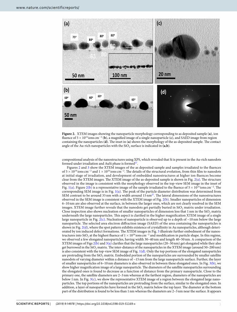
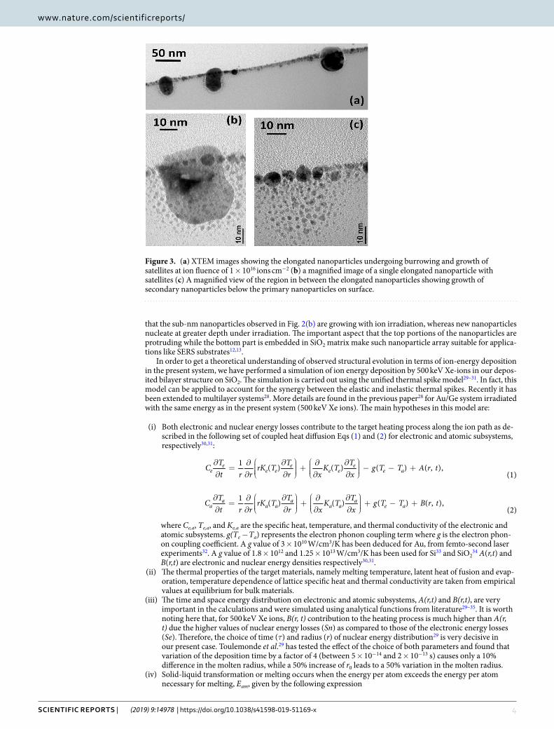
Figures 2 and 3 show the XTEM images of the as deposited sample and samples irradiated to the fluences of 5 × 10¹⁴ ions cm−2 and 1 × 10¹⁶ ions cm−2. The details of the structural evolution, from thin film to nanodots at initial stage of irradiation, and development of embedded nanostructures at higher ion fluences become clear from the XTEM images. The XTEM image of the as-deposited sample is shown in Fig. 2(a). The structure observed in the image is consistent with the morphology observed in the top-view SEM image in the inset of Fig. 1(a). Figure 2(b) is a representative image of the sample irradiated to the fluence of 5 × 10¹⁴ ions cm−2. The corresponding SEM image is in Fig. 1(a). The peak of the particle diameter distribution was determined from SEM contrast to be around 35 nm with a width around 15 nm27. The lateral dimensions of the nanostructures observed in the SEM image is consistent with the XTEM image of Fig. 2(b). Smaller nanoparticles of dimension 6–10 nm are also observed at the surface, in between the larger ones, which are not clearly resolved in the SEM images. XTEM image further reveals that the nanodots get partially buried in SiO2 matrix under irradiation. Close inspection also shows nucleation of smaller nanoparticles of dimension less that 1 nm in the SiO2 matrix underneath the large nanoparticles. This aspect is clarified in the higher magnification XTEM image of a single large nanoparticle in Fig. 2(c). Nucleation of nanoparticle is observed up to a depth of ~10 nm below the large nanoparticle. The selected area electron diffraction image (SAED) of the area containing the nanoparticles is shown in Fig. 2(d), where the spot pattern exhibits existence of crystallinity in Au nanoparticles, although deteri-orated by ion induced defect formations. The XTEM images in Fig. 3 illustrate further embedment of the nanos-tructures into SiO2 at the highest fluence of 1 × 10¹⁶ ions cm−2 and modification in particle shape. In this regime, we observed a few elongated nanoparticles, having width 30–40 nm and length 40–50 nm. A comparison of the XTEM images of Figs 2(b) and 3(a) clarifies that the large nanoparticles (20–50 nm) get elongated while they also get burrowed in the SiO2 matrix. The inter-distance of the nanoparticles in the XTEM image (around 50–200 nm) is also consistent with the top-view SEM image of Fig. 1(d). Only the top portions of the elongated nanoparticles are protruding from the SiO2 matrix. Embedded portion of the nanoparticles are surrounded by smaller satellite nanodots of varying diameter within a distance of ~15 nm from the large nanoparticle surface. Further, the layer of smaller nanoparticles of 6–10 nm diameters is also observed in between these elongated ones. In Fig. 3(b), we show higher magnification image of a large nanoparticle. The diameters of the satellite nanoparticles surrounding the elongated ones is found to decrease as a function of distance from the primary nanoparticle. Close to the primary one, the satellite diameters are 2–3 nm whereas at the farthest region, diameters of the nanoparticles are below 1 nm. In Fig. 3(c), we show the representative XTEM image of a region between the elongated large nano-particles. The top portions of the nanoparticles are protruding from the surface, similar to the elongated ones. In addition, a layer of nanoparticles have formed in the SiO2 matrix below the top layer. The diameter at the bottom part of the distribution is found to be less than 1 nm whereas the diameters are 2–3 nm near the surface. It appears
Figure 2. XTEM images showing the nanoparticle morphology corresponding to as deposited sample (a), ion fluence of 5 × 10¹⁴ ions cm−2 (b), a magnified image of a single nanoparticle (c), and SAED image from region containing the nanoparticles (d). The inset in (a) shows the morphology of the as-deposited sample. The contact angle of the Au-rich nanoparticles with the SiO2 surface is indicated in (a,b).
4Scientific RepoRtS | (2019) 9:14978 | https://doi.org/10.1038/s41598-019-51169-x
www.nature.com/scientificreportswww.nature.com/scientificreports/
that the sub-nm nanoparticles observed in Fig. 2(b) are growing with ion irradiation, whereas new nanoparticles nucleate at greater depth under irradiation. The important aspect that the top portions of the nanoparticles are protruding while the bottom part is embedded in SiO2 matrix make such nanoparticle array suitable for applica-tions like SERS substrates12,13.
In order to get a theoretical understanding of observed structural evolution in terms of ion-energy deposition in the present system, we have performed a simulation of ion energy deposition by 500 keV Xe-ions in our depos-ited bilayer structure on SiO2. The simulation is carried out using the unified thermal spike model29–31. In fact, this model can be applied to account for the synergy between the elastic and inelastic thermal spikes. Recently it has been extended to multilayer systems28. More details are found in the previous paper28 for Au/Ge system irradiated with the same energy as in the present system (500 keV Xe ions). The main hypotheses in this model are:
(i) Both electronic and nuclear energy losses contribute to the target heating process along the ion path as de-scribed in the following set of coupled heat diffusion Eqs (1) and (2) for electronic and atomic subsystems, respectively30,31:
∂∂
=∂∂
∂∂
+
∂∂
∂∂
− − +C T
t r rrK T T
r xK T T
xg T T A r t1 ( ) ( ) ( ) ( , ),
(1)ee
e ee
e ee
e a
∂∂
=∂∂
∂∂
+
∂∂
∂∂
+ − +C T
t r rrK T T
r xK T T
xg T T B r t1 ( ) ( ) ( ) ( , ),
(2)aa
a aa
a aa
e a
where Ce,a, Te,a, and Ke,a are the specific heat, temperature, and thermal conductivity of the electronic and atomic subsystems. g(Te − Ta) represents the electron phonon coupling term where g is the electron phon-on coupling coefficient. A g value of 3 × 10¹⁰ W/cm3/K has been deduced for Au, from femto-second laser experiments32. A g value of 1.8 × 10¹² and 1.25 × 10¹³ W/cm3/K has been used for Si33 and SiO2
34 A(r,t) and B(r,t) are electronic and nuclear energy densities respectively30,31.
(ii) The thermal properties of the target materials, namely melting temperature, latent heat of fusion and evap-oration, temperature dependence of lattice specific heat and thermal conductivity are taken from empirical values at equilibrium for bulk materials.
(iii) The time and space energy distribution on electronic and atomic subsystems, A(r,t) and B(r,t), are very important in the calculations and were simulated using analytical functions from literature29–35. It is worth noting here that, for 500 keV Xe ions, B(r, t) contribution to the heating process is much higher than A(r, t) due the higher values of nuclear energy losses (Sn) as compared to those of the electronic energy losses (Se). Therefore, the choice of time (τ) and radius (r) of nuclear energy distribution29 is very decisive in our present case. Toulemonde et al.29 has tested the effect of the choice of both parameters and found that variation of the deposition time by a factor of 4 (between 5 × 10⁻¹⁴ and 2 × 10⁻¹³ s) causes only a 10% difference in the molten radius, while a 50% increase of r0 leads to a 50% variation in the molten radius.
(iv) Solid-liquid transformation or melting occurs when the energy per atom exceeds the energy per atom necessary for melting, Eam, given by the following expression
Figure 3. (a) XTEM images showing the elongated nanoparticles undergoing burrowing and growth of satellites at ion fluence of 1 × 10¹⁶ ions cm−2 (b) a magnified image of a single elongated nanoparticle with satellites (c) A magnified view of the region in between the elongated nanoparticles showing growth of secondary nanoparticles below the primary nanoparticles on surface.

5Scientific RepoRtS | (2019) 9:14978 | https://doi.org/10.1038/s41598-019-51169-x
www.nature.com/scientificreportswww.nature.com/scientificreports/
∫= +E C T dT L( ) ,(3)am
T
Ts m
initial
melting
Here the first term represents the energy necessary to reach the melting temperature, where Cs(T) is the lat-tice specific heat. Lm is latent heat of fusion. The melting energies per atom, Eam, are: 0.43, 0.84, and 0.38 eV/atom for Au, Si and SiO2, respectively.
(v) For multilayer systems, the interface between materials is supposed to be consisting of a perfectly plane surface and no intermixed region exists as shown in Fig. 2.
(xvi) The electronic and nuclear energy loss are assumed to be independent of depth along each material, which is true when dealing with very thin layers as discussed previously28 (in the present case Au and Si are only 6 nm each).
The calculation code solves numerically the electronic and atomic heat diffusion Eqs (1) and (2), and provides the space and time evolution of energy per target atom, which is equivalent to temperature, as the main output. The calculations were performed in superheating scenario36. In Fig. 4 we show the evolution of the energy per atom versus time for different radial distances from the ion track for 500 keV Xe ion irradiation in Au(6 nm)/Si(6 nm) bilayer on SiO2 substrate. The horizontal black lines show melting energy per atom Eam for each of the materials. The results clearly show that in our experimental situation a molten zone is formed in Au layer and SiO2 around the ion track. However, the energy per atom is slightly lower that that required for melting for the Si layer. The radii of the molten zones are 4.5 nm and 2.5 nm for the Au and SiO2 layers, respectively. However, if we consider the phenomenon of melting point depression with the reduction of the size of the material to few nano-metres, the energy required for melting might be much lower than that for bulk materials. Consequently, even Si with 6 nm thickness might thought of, qualitatively, to exhibit melting after 500 keV Xe ions irradiation. Further, the bilayer is converted into Au-rich nanoparticles in the initial stage. Subsequently, melting can be assumed to take place along the ion track in both the nanoparticle and SiO2 matrix, although the redii of molten zones can be different. Thus, it can be inferred that the dewetting of the Au layer leading to nanoscale islands and consequent structural transitions is largely influenced by formation of molten zones due to ions energy deposition. Below we discuss the observed evolution in terms of the results of the simulation.
The ion-induced dewetting of process of the deposited bi-layer in the initial stage was discussed previously27. However, the important issue of melting of the materials along the ion track in the Au and Si layer had not been addressed through quantitative theoretical estimation, which we have shown here. The formation mechanism of
Figure 4. Evolution of the maximum energy per atom, Eamax,for different radial distances from the ion path in Au(6 nm)/Si(6 nm)/SiO2(substrate) target under 500 keV Xe ion irradiation. The horizontal dashed dot lines indicate the melting energy per atom Eam(Au), Eam(Si) and Eam(SiO2) for Au, Si and SiO2, respectively. The vertical dashed dot lines show theAu/Si and Si/SiO2 interfaces. The schematic at the bottom of the figure shows the multilayer structure as well as the cylindrical symmetry of the energy deposition of an incident ion on both electronic and atomic subsystems. The energy per atom (or lattice temperature) is the highest at the impact position and gradually decreases with radial distance, as illustrated with the red colour nuance.

6Scientific RepoRtS | (2019) 9:14978 | https://doi.org/10.1038/s41598-019-51169-x
www.nature.com/scientificreportswww.nature.com/scientificreports/
nanoscale extended structures/islands from a Au-Si bilayer in the initial stage is primarily the ion-beam-induced dewetting of the top metal layer, which is driven by ion energy deposition18–22. The evolution process is further influenced by ion beam induced mixing of Au and Si, and sputter-erosion of materials from the surface27,28. The simulation above has clearly shown that energy loss of incident ions within the bilayer leads to formation of a localized molten zone along the ion track, which persists for a time of the order of picoseconds. On the other hand, the surface tension of molten Au also differs from that of solid state. The surface tension gradient and pressure gradient within the molten zone induce flow of the material from the molten track to the surface of the top layer18,19. Overall result of material flow is similar to the dewetting of a liquid layer on a non-wetting solid surface, which results in rupture of a continuous liquid film. Array of extended structures and islands are devel-oped from a metal layer by nucleation of dry patches in the layer18–20 or by amplification of thermally generated amplitude fluctuations21,22. The extended structures subsequently evolve into regular circularly shaped particles/dots by mechanism such as Rayleigh instability37. At the same time, continuing ion irradiation leads to burrowing of the nanoparticles.
Burrowing of nanoparticles into a substrate under ion irradiation has been observed in previous studies, for instance, by Hu et al. for 800 keV Kr-ion irradiation on Pt thin film on SiO2 and Al2O3
38, and by Prakash et al. for 150 keV Ar-ion irradiation on Au thin film deposited on polymer matrix23,39. Burrowing of nanostructures on a substrate surface can be understood by the thermodynamic instability of the structures. When the interface energy of a metal nanoparticle and the substrate is smaller than the surface free energy of the metal in ambient, the nanoparticle is thermodynamically unstable. If the metal atoms get enough mobility then the nanostructures can get buried in the substrate in order to minimize the free energy23,38–41. Thermal treatment or ion irradiation greatly enhances atomic mobility within the nanostructures. As a matter of fact, we have shown above through numerical simulation of the present experimental situation that ion irradiation induces formation of ion track of a few nm radius which remains effectively in molten state for picosecond time. It has been observed that esti-mated ion track radius is ~4.5 nm in Au and 2.5 nm in SiO2 [see Fig. 4]. To associate the observed burrowing with this theoretical origin, we determine the contact angles of the nanoparticles on SiO2 from the XTEM images. If a particle makes a contact angle θc with a substrate, then the local equilibrium condition for the particle is γp + γps cos θc = γs, where γp and γs are the surface free energies of the particle and the substrate, respectively, and γps is the free energy of the interface. The angle of the as-deposited thin film comprising of nano-islands are found to be 75°–80°, on the average, as shown in Fig. 3(a), so the contact angle is π - 75° = 105°. The free energy of Au at melting temperature40 is 1.39 J m−2 and γs for SiO2 is 0.31 J m−2 at melting point38. Using these values and the con-tact angle θc, the interface energy γps is found to be 0.67 J m−2, which is much less that γp for Au. For ion irradiated Au nanoparticle in SiO2, the interface energy was found to be 0.1–0.2 J m−2 by Rizza et al.42, which is comparable to our estimated value. It should be mentioned here that the surface free energy of free Au nanoparticle has been found to be 8.78 J m−2 39, which is much greater than that of the bulk Au. If this value is considered, the surface energy of Au nanoparticle embedded in SiO2 will be significantly lower24,39. It is further observed from Fig. 3(b) that the angle between the partially embedded Au and the substrate surface decreases to 60°, making the contact angle 120°, which indicates irradiation induced decrease in interface energy. So the observed burrowing of the Au-Si nanoparticles can be attributed to reduction in surface free energy of the nanostructures in SiO2, because metal atoms in the nanoparticles are mobile in the molten ion track.
Elongation of spherical metal nanoparticles embedded in insulators, in the direction of ion irradiation, is well studied in case of Swift heavy ion irradiation where electronic energy loss dominates the ion-target interac-tion43–45. It is interpreted as a result of flow of metal atoms of the nanoparticles for in-plane stress release. Material flow is induced in a molten zone formed around the ion track through the metal nanoparticles and transition of spherical nanoparticles to elongation shape takes place by consecutive effect of many ions. Elongation of spher-ical nanoparticles in low ion energy regime where nuclear energy loss gives a significant contribution to energy deposition was however observed, for instance, in case of Au nanoparticles in SiO2 under 3 MeV Au ion irradia-tion46. In the present study, we see that elongation sets in subsequent to onset of burrowing of the nanoparticles [Figs 2(b) and 3(a)]. Our numerical simulation demonstrates molten zone formation around the ion track in the Au as well as in SiO2, with diameters 4.5 nm and 2.5 nm, respectively. Therefore material flow can be induced in the molten zone leading to elongation of the nanoparticles and this process may occur parallel to burrowing.
Ridgway et al. reported45 that, under swift heavy ion irradiation on metal nanoparticles embedded in SiO2, spherical nanoparticles having diameter above a critical value get elongated, whereas nanoparticles having diam-eter below may get dissolved. The critical value is related to ion track diameter in SiO2 and for Au nanoparticles it is within 10–11 nm. In our experiment, we observe the lateral dimensions of the elongated Au nanoparticles are much larger, 30–40 nm. Further, diameter of molten ion track in SiO2 (2.5 nm) is smaller than that in Au(4.5 nm).However, the fact that smaller nanoparticles having diameters 6–10 nm [Fig. 3(a,c)] does not undergo elongation, was also observed by Ridgeway et al.45. It is also to be noted that the ion fluence applied in the present experiment, where nuclear energy loss dominates, is two-order-of-magnitude higher than that applied in swift heavy ion experiments. We assume that in low energy ion irradiation, elongation of nanoparticles proceeds in a cumulative by increasing no of ions going through the nanoparticles but is still related to material flow in the molten ion track in Au and SiO2. Since the larger nanoparticles (30–40 nm diameter) have a larger in-plane areal density compared to smaller, 6–10 nm nanoparticles, higher number of atoms goes through the larger nanoparticles and induce the shape transformation while smaller nanoparticles retains spherical shape. Our study, however, shows that molten-ion-track-induced elongation can also be active process in the nuclear stopping regime. Further the dissolution of Au atoms into SiO2 matrix can take place through flow in the molten track and also from ballistic ejection due to nuclear energy loss from both the larger and smaller nanoparticles.
Subsequent to burrowing, we observe nucleation and growth of small nanoparticles below the larger ones [Figs 3 and 4]and appearance of satellite nanoparticles around the elongated ones. Nucleation of metal nano-particles in insulator matrix under ion irradiation was studies by several groups42,47–51. Nanoparticles nucleate in
7Scientific RepoRtS | (2019) 9:14978 | https://doi.org/10.1038/s41598-019-51169-x
www.nature.com/scientificreportswww.nature.com/scientificreports/
the matrix when the concentration of metal atoms (Au in present case)getting dissolved in the matrix from the primary nanoparticles by ballistic ejection or melting in ion track exceeds supersaturation limit. Under ion irra-diation, the concentration of ejected atoms CI(R0) near the interface of a nanoparticle with the matrix of radius R0 is given by CI(R0) = C∞
I (1 + RCI/R0)49. Here C∞
I is the concentration of solutes near a planer interface, and RCI
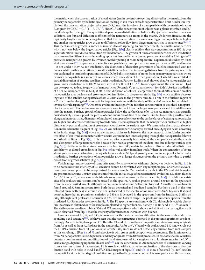
is called capillarity length. The quantities depend upon distribution of ballistically ejected atoms due to nuclear collisions, ion flux and diffusion coefficient of the nanoparticle atoms in the matrix. Under ion irradiation, the capillarity length may become negative so that the concentration of atoms near bigger nanoparticles is higher and smaller nanoparticles grow at due to diffusional solute flow from bigger nanoparticles to smaller ones42,47–50. This mechanism of growth is known as inverse Owsald ripening. In our experiment, the smaller nanoparticles which nucleate below the bigger nanoparticles [Fig. 2(b)] clearly exhibits that Au concentration in SiO2 is over supersaturation limit due to dissolution by incident ions. The growth of nucleated nanoparticles with irradiation may proceed in different ways depending upon ion flux and irradiation temperature. A model by Heinig et al.49 predicted nanoparticle growth by inverse Oswald ripening at room temperature. Experimental studies by Rizza et al. also showed42,47 appearance of satellite nanoparticles around primary Au nanoparticles in SiO2 of diameter ~15 nm under 4 MeV Au ion irradiation. The diameters of these first generations of satellites increased with ion fluence while further generations of smaller satellites nucleated at increasing distance from the primary one. This was explained in terms of superaturation of SiO2 by ballistic ejection of atoms from primary nanoparticles where primary nanoparticle is a source of Au atoms where nucleation of further generation of satellites was related to partial dissolution of existing satellites under irradiation. Further, Ruffino et al. showed that Au nanoparticles can grow under irradiation of 200 keV Ar-ions ions at low flux of 1.4 μA52. In our experiment, the ion flux of 1.4 μA can be expected to lead to growth of nanoparticles. Recently Vu et al. has shown53 for 4 MeV Au-ion irradiation of 4 nm Au nanoparticles in SiO2 at 300 K that diffusion of solutes is larger than thermal diffusion and smaller nanoparticles may nucleate and grow under ion irradiation. In the present study, Fig. 3(b) which exhibits decreas-ing radii of the satellite nanoparticles from 2–3 nm close to the primary ones to <1 nm in the furthest region of ~15 nm from the elongated nanoparticles is quite consistent with the study of Rizza et al. and can be correlated to inverse Oswald ripening47,48. Observed evolution thus signify the fact that concentration of dissolved nanoparti-cles increase with fluence because Au atoms are knocked out from the larger nanoparticles and the satellite ones into the matrix. Further, growth of nanoparticles below the surface layer of 6–10 nm Au nanoparticles partially buried in SiO2 is also support the picture of continuous dissolution of Au atoms. Similar to satellite growth around elongated nanoparticles, diameters of nucleated nanoparticles close to the surface layer of existing nanoparticles are higher and decrease continuously towards bulk. It seems plausible that the nanoparticles nucleated at higher distances by partial dissolution of grown particles close to the surface layer. We summarise the structural evolu-tion in the schematic diagram of Fig. 5(a–c). Au-rich nanoparticle array is formed on SiO2 by ion beam dewetting at the initial stage [Fig. 5(a)] where smaller nanoparticles are in between the larger nanoparticles. Under cumula-tive effect of ion irradiation material flow occurs within molten ion track going through the nanoparticles [shown as dashed red lines in Fig. 5(a)]. This causes two effects, namely burrowing of the nanoparticles into the matrix and elongation of large nanoparticles because they receive grater no of incident ions due to larger surface area [Fig. 5(b)]. At the same time, Au atoms are dissolved into SiO2 matrix by nuclear collision induced ballistic pro-cess [shown as dotted green lines in Fig. 5(a–c)] as well as flow in molten track. When the concentration of solute atoms goes over supersaturation, nanoparticles nucleate in SiO2 and grow by continuous supply of solutes under irradiation. Further generations of nanoparticles grow at larger distances from the primary ones due to partial dissolution of grown satellites [Fig. 5(b,c)].
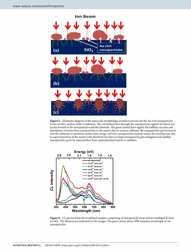
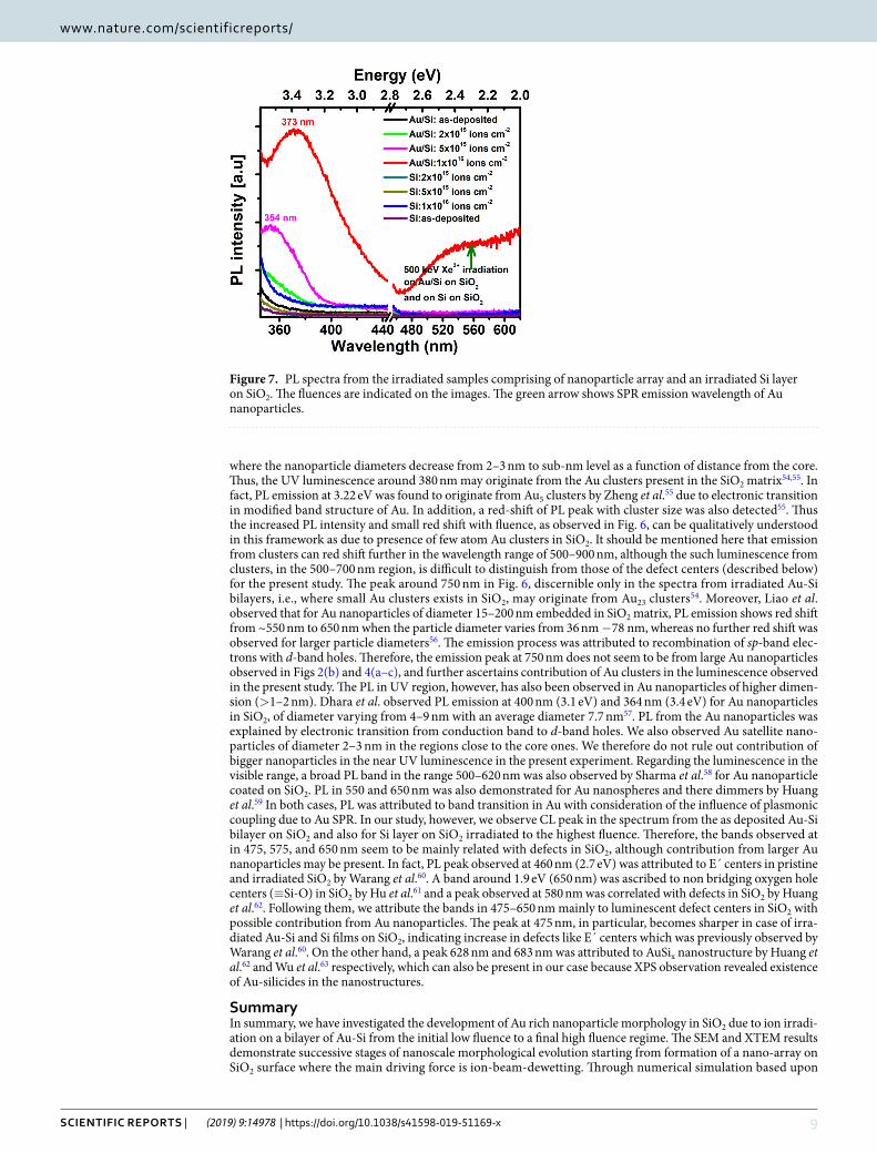
Visible range luminescence of composite nano-dot array evolves with morphology as depicted in Fig. 6. It is to be noted here that intensity of CL emission cannot be correlated with any morphological or structural evolu-tion since the setup had to be re-optimized for every sample. Two emission bands in the UV and visible region are prominent around 380 nm and 650 nm from the initial stage of nanostructural evolution, i.e., from fluence 5 × 10¹⁴ ions cm−2, where nanoscale islands are observed to grow on the surface [Fig. 1(a)]. In addition, exist-ence of a peak around 475 nm can be traced in the spectra. A peak is present around 650 nm in the spectrum from the as-deposited sample although no emission band around 380 nm is observed. A small emission band is found around 575 nm in spectra from both the as-deposited and irradiated samples. Further, a band in the near infrared range with peak at around 750 nm is observed in the spectra of ion irradiated Au-Si bilayers. It should be noted here that no prominent emission at 380 nm is detected in the spectrum from the irradiated Si film on SiO2 although faint peaks are discernible at 475, 575 and 650 nm range. The photoluminescence spectra from the irradiated Au-Si samples are shown in Fig. 7. The PL spectra are consistent with CL, although detectable photo-luminescence is obtained only for samples implanted to higher fluences, namely, 5 × 10¹⁵ and 1 × 10¹⁶ ions cm−2. The visible peaks are discernible at 354 and 373 nm respectively, which show a red shift with increasing fluence. It is also observed from Fig. 7 that the intensity of luminescence increases with fluence.
Luminescence of Au, Si, and SiO2 is correlated with the structural modification in the nanoscale and corre-sponding band structure54,55. We have seen that the nanostructures observed in the present experiment are dom-inatingly Au with AuSi phase present27. Thus the CL and PL from these composite nanostructures may originate from Au as well as from AuSi phase in the nanoscale. As for the UV band with peak around 380 nm, we rule out the CL/PL emission from SiO2 or ion irradiated Si/SiO2 since we do not detect any emission from such samples at this wavelength [Figs 6 and 7] and associate it with Au or AuSi composite nanostructure. The luminescence from Au nanoparticles is size dependent and may originate from different processes. In case of few atoms clusters, quantum confinement and modification of band structures of Au can give rise to luminescence in the UV to visible range, depending upon the cluster size54,55. On the other hand, in Au nanoparticles of dimensions varying from a few nm to tens of nanometers, PL is associated with radiative recombination of the electrons in the con-duction band with holes in the d-band55. XTEM images of Figs 3(b) and 4(a–c) show a few small (<1 nm) satellite nanoparticles at the initial stage of evolution and growth of large number of satellite nanoparticles at the late stage,
8Scientific RepoRtS | (2019) 9:14978 | https://doi.org/10.1038/s41598-019-51169-x
www.nature.com/scientificreportswww.nature.com/scientificreports/
Figure 5. Schematic diagram of the nanoscale morphology evolution process (a) the Au-rich nanoparticles forms on SiO2 surface under irradiation. The red dashed lines through the nanoparticles signify the latent ion tracks formed in the nanoparticles and the substrate. The green dotted lines signify the ballistic ejection and dissolution of atoms from nanoparticles to the matrix due to nuclear collisions (b) nanoparticles get burrowed into the substrate to minimize surface free energy and new nanoparticles nucleate under the existing ones due to supersaturation of the matrix with dissolved Au toms (c) large nanoparticles gets elongated and satellite nanoparticles grow by material flow from supersaturated matrix to satellites.
Figure 6. CL spectra from the irradiated samples comprising of nanoparticle array and an irradiated Si layer on SiO2. The fluences are indicated on the images. The green arrow shows SPR emission wavelength of Au nanoparticles.
9Scientific RepoRtS | (2019) 9:14978 | https://doi.org/10.1038/s41598-019-51169-x
www.nature.com/scientificreportswww.nature.com/scientificreports/
where the nanoparticle diameters decrease from 2–3 nm to sub-nm level as a function of distance from the core. Thus, the UV luminescence around 380 nm may originate from the Au clusters present in the SiO2 matrix54,55. In fact, PL emission at 3.22 eV was found to originate from Au5 clusters by Zheng et al.55 due to electronic transition in modified band structure of Au. In addition, a red-shift of PL peak with cluster size was also detected55. Thus the increased PL intensity and small red shift with fluence, as observed in Fig. 6, can be qualitatively understood in this framework as due to presence of few atom Au clusters in SiO2. It should be mentioned here that emission from clusters can red shift further in the wavelength range of 500–900 nm, although the such luminescence from clusters, in the 500–700 nm region, is difficult to distinguish from those of the defect centers (described below) for the present study. The peak around 750 nm in Fig. 6, discernible only in the spectra from irradiated Au-Si bilayers, i.e., where small Au clusters exists in SiO2, may originate from Au23 clusters54. Moreover, Liao et al. observed that for Au nanoparticles of diameter 15–200 nm embedded in SiO2 matrix, PL emission shows red shift from ~550 nm to 650 nm when the particle diameter varies from 36 nm −78 nm, whereas no further red shift was observed for larger particle diameters56. The emission process was attributed to recombination of sp-band elec-trons with d-band holes. Therefore, the emission peak at 750 nm does not seem to be from large Au nanoparticles observed in Figs 2(b) and 4(a–c), and further ascertains contribution of Au clusters in the luminescence observed in the present study. The PL in UV region, however, has also been observed in Au nanoparticles of higher dimen-sion (>1–2 nm). Dhara et al. observed PL emission at 400 nm (3.1 eV) and 364 nm (3.4 eV) for Au nanoparticles in SiO2, of diameter varying from 4–9 nm with an average diameter 7.7 nm57. PL from the Au nanoparticles was explained by electronic transition from conduction band to d-band holes. We also observed Au satellite nano-particles of diameter 2–3 nm in the regions close to the core ones. We therefore do not rule out contribution of bigger nanoparticles in the near UV luminescence in the present experiment. Regarding the luminescence in the visible range, a broad PL band in the range 500–620 nm was also observed by Sharma et al.58 for Au nanoparticle coated on SiO2. PL in 550 and 650 nm was also demonstrated for Au nanospheres and there dimmers by Huang et al.59 In both cases, PL was attributed to band transition in Au with consideration of the influence of plasmonic coupling due to Au SPR. In our study, however, we observe CL peak in the spectrum from the as deposited Au-Si bilayer on SiO2 and also for Si layer on SiO2 irradiated to the highest fluence. Therefore, the bands observed at in 475, 575, and 650 nm seem to be mainly related with defects in SiO2, although contribution from larger Au nanoparticles may be present. In fact, PL peak observed at 460 nm (2.7 eV) was attributed to E´ centers in pristine and irradiated SiO2 by Warang et al.60. A band around 1.9 eV (650 nm) was ascribed to non bridging oxygen hole centers (≡Si-O) in SiO2 by Hu et al.61 and a peak observed at 580 nm was correlated with defects in SiO2 by Huang et al.62. Following them, we attribute the bands in 475–650 nm mainly to luminescent defect centers in SiO2 with possible contribution from Au nanoparticles. The peak at 475 nm, in particular, becomes sharper in case of irra-diated Au-Si and Si films on SiO2, indicating increase in defects like E´ centers which was previously observed by Warang et al.60. On the other hand, a peak 628 nm and 683 nm was attributed to AuSix nanostructure by Huang et al.62 and Wu et al.63 respectively, which can also be present in our case because XPS observation revealed existence of Au-silicides in the nanostructures.
SummaryIn summary, we have investigated the development of Au rich nanoparticle morphology in SiO2 due to ion irradi-ation on a bilayer of Au-Si from the initial low fluence to a final high fluence regime. The SEM and XTEM results demonstrate successive stages of nanoscale morphological evolution starting from formation of a nano-array on SiO2 surface where the main driving force is ion-beam-dewetting. Through numerical simulation based upon
Figure 7. PL spectra from the irradiated samples comprising of nanoparticle array and an irradiated Si layer on SiO2. The fluences are indicated on the images. The green arrow shows SPR emission wavelength of Au nanoparticles.

1 0Scientific RepoRtS | (2019) 9:14978 | https://doi.org/10.1038/s41598-019-51169-x
www.nature.com/scientificreportswww.nature.com/scientificreports/
a thermal spike model, we have demonstrated formation of molten ion-tracks in Au and SiO2 which results in dewetting. The simulation result, combined with XTEM results indicates that dewetting is initiated by formation of dry patches. We have shown gradual burrowing of the nanoparticles into SiO2 subsequent to formation of nanoparticle array on the surface and simultaneous elongation of large nanoparticles in the direction of incident ions, where the required atomic mobility is provided by ion-induced latent ion track formation. Our experi-mental findings also confirm that the burrowing is caused by tendency of the system towards minimization of surface energy. Growth of satellite nanoparticles of varying diameter around the embedded larger particles by inverse Oswald ripening is shown to accompany the burrowing effect. We have also shown UV and Visible range luminescence in the ion-beam-synthesized nanostructured materials. The observed luminescence is understood to originate from nanoscale Au particles in SiO2 at different stages of ion irradiation, which shows the potential of ion beam processing in synthesis of UV-infrared luminescent embedded nanostructures. Since protrusion of developed nanostructures over the matrix has been shown, our results are further promising for technological application such as surface enhanced Raman scattering.
Received: 11 March 2019; Accepted: 17 September 2019;Published: xx xx xxxx
References 1. Shipway, A. N., Katz, E. & Willner, I. Nanoparticle Arrays on Surfaces for Electronic, Optical and Sensor applications. Chem Phys
Chem 1, 18–52 (2000). 2. Metal Nanoparticles: Synthesis, Characterization, and Application (ed. Feldheim, D. L. & Foss, C. A. Jr.) (Marcel Dekker, Inc. New
York 2002). 3. Linic, S., Christopher, P. & Ingram, D. B. Plasmonic-metal nanostructures for efficient conversion of solar to chemical energy. Nature
Mat. 10, 911–921 (2011). 4. Priolo, F., Gregorkiewicz, T., Gallli, M. & Krauss, T. F. Silicon nanostructures for photonics and photovoltaics. Nature Nanotech. 9,
19–32 (2014). 5. Jiang, R., Li, B., Fang, C. & Wang, J. Metal/Semiconductor Hybrid Nanostructures for Plasmon-Enhanced Applications. J. Adv.
Mater. 26, 5274–5309 (2014). 6. Hou, W. & Cronin, S. B. A Review of Surface Plasmon Resonance-Enhanced Photocatalysis. Adv. Funct. Mater. 23, 1612–1619
(2013). 7. Wei, H. & Xu, H. Plasmonics in composite nanostructures. Mater. Today. 17, 372–380 (2014). 8. Ingram, D. & Linic, S. Water Splitting on Composite Plasmonic Metal/Semiconductor Photoelectrodes: Evidence for Selective
Plasmon-Induced Formation of Charge Carriers near the Semiconductor Surface. J. Am. Chem. Soc. 133, 5202–5205 (2011). 9. Spadavecchia, J., Prete, P., Lovergine, N., Tapfer, L. & Rella, R. Au Nanoparticles Prepared by Physical Method on Si and Sapphire
Substrates for Biosensor Applications. J. Phys. Chem. B 109, 17347–17349 (2005). 10. Hiep, H. M., Yoshikawa, H., Sato, M. & Tamiya, E. An Interference Localized Surface Plasmon Resonance Biosensor Based on the
Photonic Structure of Au Nanoparticles and SiO2/Si Multilayers. ACS Nano. 3, 446–452 (2009). 11. Jung, K.-Y., Teixeira, F. L. & Reano, R. M. Au/SiO2 Nanoring Plasmon Waveguides at Optical Communication Band. J. Light.
Technol. 25, 2757–2765 (2007). 12. Si, S. et al. Facile Fabrication of High-Density Sub-1-nm Gaps from Au Nanoparticle Monolayers as Reproducible SERS Substrates.
Adv. Funct. Mater. 26, 8137–8145 (2016). 13. Tian, F., Bonnier, F., Cassey, A., Shanahan, A. E. & Byrne, H. J. Surface enhanced Raman scattering with gold nanoparticles: effect of
particle shape. Anal. Methods. 6, 9116–9123 (2014). 14. Pasa, A. A., Paes, H. Jr. & Losch, W. Au/Si interface: Experiments on substrate influence. J. Vac. Sci. Technol. 10, 374–380 (1992). 15. Khalfaoui, R., Benazzouz, C., Guittoum, A., Tabet, N. & Tobbeche, S. Irradiation-induced silicide formation in the ion beam-mixed
Au/Si(1 0 0) system at room temperature. Vacuum. 78, 223–227 (2005). 16. Mukherjee, S. et al. Hot-Electron-Induced Dissociation of H2 on Gold Nanoparticles Supported on SiO2. J. Am. Chem. Soc. 136,
64–67 (2014). 17. Babor, R. et al. Real-time observation of self-limiting SiO2/Si decomposition catalysed by gold silicide droplets. RSC Advances. 5,
101726 (2015). 18. Hu, X., Cahill, D. G. & Averback, R. S. Nanoscale pattern formation in Pt thin films due to ion-beam-induced dewetting. Appl. Phys.
Lett. 76, 3215–3219 (2000). 19. Hu, X., Cahill, D. G. & Averback, R. S. Dewetting and nanopattern formation of thin Pt films on SiO2 induced by ion beam
irradiation. J. Appl. Phys. 89, 7777–7783 (2001). 20. Hu, X., Cahill, D. G. & Averback, R. S. In situ transmission electron microscopy study of irradiation induced dewetting of ultrathin
Pt films. J. Appl. Phys. 93, 165–169 (2003). 21. Repetto, L., Firpo, B., Piano, G., Valbusa, E. & Ion, U. induced spinoidal dewetting of thin solid films. Appl. Phys. Lett. 100, 223113–4
(2012). 22. Repetto, L., Savio, R. L., Batic, B. S., Firpo, G. & Valbusa, U. Role of surface morphology on ion induced dewetting of thin solid films.
Appl. Surf. Sci. 315, 432439 (2014). 23. Prakash, J. et al. Synthesis of Au nanoparticles at the surface and embedded in carbonaceous matrix by 150 keV Ar ion irradiation.
J. Phys.D: Appl. Phys. 44, 125302–8 (2011). 24. Meng, X., Shibayama, T., Yu, R., Takayanagi, S. & Watanabe, S. Ion irradiation synthesis of Ag–Au bimetallic nanospheroids in SiO2
glass substrate with tunable surface plasmon resonance frequency. J. Appl. Phys. 114, 054308–9 (2013). 25. Datta, D. P. et al. Ion-beam-induced nanodots formation from Au/SI films on quartz surface. Nuclear Instrum. and Meth. in Phys.
Res. B. 379, 48–51 (2016). 26. Datta, D. P., Siva, V., Singh, A., Kanjilal, D. & Sahoo, P. K. Photoluminescent Au-Ge composite nanodots formation on SiO2 surface
by ion induced dewetting. Nuclear Instrum. and Meth. in Phys. Res. B. 407, 141–144 (2017). 27. Datta, D. P., Siva, Varma, S., Kanjilal, D. & Sahoo, P. K. Ion induced dewetting of Au–Si on a SiO2 surface: composite nanodot
evolution and wettability transition. Phys. Chem. Chem. Phys. 18, 2995529960 (2016). 28. Datta, D. P., Chettah, A., Siva, V., Kanjilal, D. & Sahoo, P. K. Dewetting induced Au-Ge composite nanodot evolution in SiO2. Appl.
Surf. Sci. 428, 676–683 (2018). 29. Toulemonde, M. et al. Phys. Rev. B 83, 054106–9 (2011). 30. Chettah, A. et al. The inelastic thermal spike model applied to metal/insulator interfaces. Phys. Status. Sol. C. 12, 102–106 (2015). 31. Mieskes, H. D. et al. Electronic and nuclear thermal spike effects in sputtering of metals with energetic heavy ions. Phys. Rev. B 67,
155414–12 (2003). 32. Brorson, S. D. et al. Femtosecond room-temperature measurement of the electron-phonon coupling constant γ in metallic
superconductors. Phys. Rev. Lett. 64, 2172–2175 (1990).

1 1Scientific RepoRtS | (2019) 9:14978 | https://doi.org/10.1038/s41598-019-51169-x
www.nature.com/scientificreportswww.nature.com/scientificreports/
33. Chettah, A. et al. Behavior of crystalline silicon under huge electronic excitations: A transient thermal spike description. Nuclear Instrum. and Meth. in Phys. Res. B. 267, 2719–2724 (2009).
34. Toulemonde, M., Dufour, C., Meftah, A. & Paumier, E. Transient thermal processes in heavy ion irradiation of crystalline inorganic insulators. Nucl. Instrum. Methods B. 166, 903 (2000).
35. Wang, Z. G., Dufour, C., Paumier, E. & Toulemonde, M. The Se sensitivity of metals under swift-heavy-ion irradiation: a transient thermal process. J. Phys.: Condens. Mater. 6, 6733–6750 (1994), errata J. Phys.: Condens. Mater. 7, 2525–2526 (1995).
36. Chettah, A. et al. Melting of Au and Al in nanometer Fe/Au and Fe/Al multilayers under swift heavy ions: A thermal spike study. Nuclear Instrum. and Meth. in Phys. Res. B. 245, 150 (2006).
37. Ruffino, F. & Grimaldi, M. G. Controlled dewetting as fabrication and patterning strategy for metal nanostructures. Phys. Stat. Sol. 212, 1662–1684 (2015).
38. Hu, X., Cahill, D. G. & Averback, R. S. Burrowing of Pt nanoparticles into SiO2 during ion-beam irradiation. J. Appl. Phys. 92, 3995–4000 (2002).
39. Prakash, J. et al. Phenomenological understanding of dewetting and embedding of noble metal nanoparticles in thin films induced by ion irradiation. Mater. Chem. Phys. 147, 920 (2014).
40. Satpati, B., Satyam, P. V., Som, T. & Dev, B. N. Ion-beam-induced embedded nanostructures and nanoscale mixing. J. Appl. Phys. 96, 5212–5216 (2004).
41. Biskupek, J., Kaiser, U. & Falk, F. Heat- and electron-beam-induced transport of gold particles into silicon oxide and silicon studied by in situ high-resolution transmission electron microscopy. J. Electron. Micro. 57, 83–89 (2008).
42. Rizza, G., Ramajauny, Y., Gacoin, T., Vieille, L. & Henry, S. Chemically synthesized gold nanoparticles embedded in a SiO2 matrix: A model system to give insights into nucleation and growth under irradiation. Phys. Rev. B. 76, 255414–9 (2007).
43. Kluth, P. et al. Energy dependent saturation width of swift heavy ion shaped embedded Au nanoparticles. Appl. Phys. Lett. 94, 113107–3 (2009).
44. Amekura, H. et al. Zn nanoparticles irradiated with swift heavy ions at low fluences: Optically-detected shape elongation induced by non-overlapping ion tracks. Phys. Rev. B. 83, 205401–10 (2011).
45. Ridgway, M. C. et al. Role of Thermodynamics in the Shape Transformation of Embedded Metal Nanoparticles Induced by Swift Heavy-Ion Irradiation. Phys. Rev. Lett. 106, 095505–4 (2011).
46. Datta, D. P., Takeda, Y., Amekura, H., Sasase, M. & Kishimoto, N. Controlled shape modification of embedded Au nanoparticles by3 MeV Au2+ -ion irradiation. Appl. Surf. Sci. 310, 164–168 (2014).
47. Rizza, G. C., Strobel, M., Heinig, K. H. & Bernas, H. Ion irradiation of gold inclusions in SiO2: Experimental evidence for inverse Ostwald ripening. Nuclear Instrum. and Meth. in Phys. Res. B 178, 78–83 (2001).
48. Rizza, G., Cheverry, H., Gacoin, T., Lamasson, A. & Henry, S. Ion beam irradiation of embedded nanoparticles: Toward an in situ control of size and spatial distribution. J. Appl. Phys. 101, 014321–7 (2007).
49. Heinig, K. H., Muller, T., Schmidt, B., Strobel, M. & Moller, W. Interfaces under ion irradiation: Growth and taming of nanostructures. Appl. Phys. A 77, 17–25 (2003).
50. Meng, X., Shibayama, T., Yu, R., Takayanagi, S. & Watanabe, S. Microstructure analysis of ion beam-induced surface nanostructuring of thin Au film deposited on SiO2. glass. J. Mat. Sci. 48, 920 (2013).
51. Meng, X., Shibayama, T., Yu, R., Ishioka, J. & Watanabe, S. Ion beam surface nanostructuring of noble metal films with localized surface plasmon excitation. Current Opinion in Solid State and Materials Science. 21, 177–186 (2017).
52. Ruffino, F. et al. Self-organization of Au nanoclusters on the SiO2 surface induced by 200 keV-Ar+ irradiation. Nuclear Instrum. and Meth. in Phys. Res. B. 257, 810 (2007).
53. Vu, T. H. Y., Ramjauny, Y., Hayoun, M., Rizza, G. & Perruchas, S. On the evolution of the steady state in gold-silica nanocomposites under sustained irradiation. J. Appl. Phys. 117, 174305–10 (2015).
54. Zheng, J., Zhang, C. & Dickson, R. M. Highly Fluorescent, Water-Soluble, Size-Tunable Gold Quantum Dots. Phys. Rev. Lett. 93, 077402–4 (2004).
55. Zheng, J., Zhou, C., Yu, M. & Liu, J. Different sized luminescent gold nanoparticles. Nanoscale. 4, 4073–4083 (2012). 56. Liao, H., Wen, W. & Wong, G. K. L. Photoluminescence from Au nanoparticles embedded in Au:oxide composite films. J. Opt. Soc.
Am. 23, 2518–2521 (2006). 57. Dhara, S. et al. Blue luminescence of Au nanoclusters embedded in silica matrix. J. Chem. Phys. 121, 12595–12599 (2004). 58. Sharma, A., Dhiman, N., Sing, B. P. & Gathania, A. K. Spectroscopic investigations on metallo-dielectric Gold@silica composites. J.
Molecule. Struc. 1074, 522–526 (2014). 59. Huang, S. et al. Photoluminescence of a Plasmonic Molecule. ACS Nano. 9, 7072–7079 (2015). 60. Warang, T. N. et al. Cathodoluminescence studies of swift heavy ion irradiated Au/SiO2/p-Si structures. Surface and Coating.
Technology. 201, 8503–8505 (2007). 61. Hu, M. et al. Photosensitive gold-nanoparticle-embedded dielectric nanowires. Nature Materials 5, 102–106 (2006). 62. Huang, L. & Wang, L. D. Preparation and Photoluminescence Properties of AuSix (x = 1/2,1/7) Nanoparticles. J. Acta Optica Sinica.
30, 2338–2343 (2010). 63. Wu, J. S. et al. Growth and Optical Proprties of Self-Organized Au2Si Nanospheres Pea-Podded in a Silicon Oxide Nanowire.
Advanced Mater. 14, 1847–1850 (2002).
AcknowledgementsD. P. Datta and P. K. Sahoo acknowledges TARE research grant from Science and Engineering Research Board (SERB), Grant No. TAR/2018/000824. The authors thank M. Toulemonde and C. Dufour, University of CAEN, France, for permitting the use of the source code for bulk and multilayer systems. Authors also thank LEIBF staff members, IUAC, New Delhi for their help during ion irradiations. Mr. V Siva, SPS, NISER is acknowledged for his help during irradiations. Dr. A. Maiti, SPMS, SINP, is acknowledged for his help with CL spectroscopy. The authors acknowledge financial support from DAE, India and NISER Bhubaneswar.
Author contributionsD.P.D. and P.K.S. conceive the ideas, designed the experiment, A.C. did the thermal spike model calculation and corresponding figures, A.M perform the Cathodoluminescence experiment, B.S. performed the XTEM and D.P.D. and P.K.S. analysed the data and wrote the manuscript.
competing interestsThe authors declare no competing interests.
Additional informationCorrespondence and requests for materials should be addressed to P.K.S.

1 2Scientific RepoRtS | (2019) 9:14978 | https://doi.org/10.1038/s41598-019-51169-x
www.nature.com/scientificreportswww.nature.com/scientificreports/
Reprints and permissions information is available at www.nature.com/reprints.Publisher’s note Springer Nature remains neutral with regard to jurisdictional claims in published maps and institutional affiliations.
Open Access This article is licensed under a Creative Commons Attribution 4.0 International License, which permits use, sharing, adaptation, distribution and reproduction in any medium or
format, as long as you give appropriate credit to the original author(s) and the source, provide a link to the Cre-ative Commons license, and indicate if changes were made. The images or other third party material in this article are included in the article’s Creative Commons license, unless indicated otherwise in a credit line to the material. If material is not included in the article’s Creative Commons license and your intended use is not per-mitted by statutory regulation or exceeds the permitted use, you will need to obtain permission directly from the copyright holder. To view a copy of this license, visit http://creativecommons.org/licenses/by/4.0/. © The Author(s) 2019
Related Documents