Citation: Franz, D.; Häfner, T.; Kunz, T.; Roth, G.-L.; Rung, S.; Esen, C.; Hellmann, R. Ultrashort Pulsed Laser Drilling of Printed Circuit Board Materials. Materials 2022, 15, 3932. https://doi.org/10.3390/ ma15113932 Academic Editors: Antonio Riveiro, Juan Pou and Félix Quintero Martínez Received: 23 March 2022 Accepted: 27 May 2022 Published: 31 May 2022 Publisher’s Note: MDPI stays neutral with regard to jurisdictional claims in published maps and institutional affil- iations. Copyright: © 2022 by the authors. Licensee MDPI, Basel, Switzerland. This article is an open access article distributed under the terms and conditions of the Creative Commons Attribution (CC BY) license (https:// creativecommons.org/licenses/by/ 4.0/). materials Article Ultrashort Pulsed Laser Drilling of Printed Circuit Board Materials Daniel Franz 1, * , Tom Häfner 2 , Tim Kunz 2 , Gian-Luca Roth 1 , Stefan Rung 1 , Cemal Esen 3 and Ralf Hellmann 1 1 Applied Laser and Photonics Group, University of Applied Sciences Aschaffenburg, Würzburger Straße 45, 63743 Aschaffenburg, Germany; [email protected] (G.-L.R.); [email protected] (S.R.); [email protected] (R.H.) 2 Schmoll Maschinen GmbH, Odenwaldstraße 67, 63322 Rödermark, Germany; [email protected] (T.H.); [email protected] (T.K.) 3 Applied Laser Technologies, Ruhr University Bochum, Universitätsstraße 150, 44801 Bochum, Germany; [email protected] * Correspondence: [email protected] Abstract: We report on a comprehensive study of laser percussion microvia drilling of FR-4 printed circuit board material using ultrashort pulse lasers with emission in the green spectral region. Laser pulse durations in the pico- and femtosecond regime, laser pulse repetition rates up to 400 kHz and laser fluences up to 11.5 J/cm 2 are applied to optimize the quality of microvias, as being evaluated by the generated taper, the extension of glass fiber protrusions and damage of inner lying copper layers using materialography. The results are discussed in terms of the ablation threshold for FR-4 and copper, heat accumulation and pulse shielding effects as a result of pulse to pulse interactions. As a specific result, using a laser pulse duration of 2 ps appears beneficial, resulting in small glass fiber protrusions and high precision in the stopping process at inner copper layer. If laser pulse repetition rates larger than 100 kHz are applied, we find that the processing quality can be increased by heat accumulation effects. Keywords: laser drilling; ultrashort pulse (USP) laser; printed circuit board (PCB); heat accumulation; pulse to pulse interactions; microvia; ablation threshold; materialography 1. Introduction A printed circuit board (PCB) is an electronic key component that requires the pro- duction of thousands vias with diameters ranging from 1 to 1000 μm[1,2]. Driven by the trend towards miniaturized high-performance electronic devices and power electronics, the electronic industry is challenged in minimizing via diameters, in turn enabling increasing wiring and interconnection densities. Mechanically produced through holes in multi-layer PCBs are an unfavorable solution because of the limited available diameter range and throughput. Thus, laser blind via drilling to inner copper layers has been established with laser beam sources such as CO 2 or pulsed UV nanosecond lasers [3–5]. These so-called microvias enable the connection of several electrically conductive copper layers of a PCB by electroplating with copper. For the separation of the copper layers, layers of FR-4 laminate (composite of epoxy resin with woven fiberglass reinforcement [6]) are widely used in the assembly fabrication of PCBs. Characterization of microvias in typical FR-4 PCB material is based on the taper (ratio of the upper to lower microvia diameter), the length of glass fiber protrusion, and the dam- age in the inner copper layer Cu damage [7–9], as illustrated in Figure 1. For the generation of microvias, firstly, the uppermost copper layer and then, secondly, the FR-4 is removed down to the inner copper layer using several laser pulses. After laser drilling, copper layers are affiliated by electroplating with copper to create electrically conductive connections. If Materials 2022, 15, 3932. https://doi.org/10.3390/ma15113932 https://www.mdpi.com/journal/materials

Welcome message from author
This document is posted to help you gain knowledge. Please leave a comment to let me know what you think about it! Share it to your friends and learn new things together.
Transcript
Citation: Franz, D.; Häfner, T.; Kunz,
T.; Roth, G.-L.; Rung, S.; Esen, C.;
Hellmann, R. Ultrashort Pulsed Laser
Drilling of Printed Circuit Board
Materials. Materials 2022, 15, 3932.
https://doi.org/10.3390/
ma15113932
Academic Editors: Antonio Riveiro,
Juan Pou and Félix Quintero
Martínez
Received: 23 March 2022
Accepted: 27 May 2022
Published: 31 May 2022
Publisher’s Note: MDPI stays neutral
with regard to jurisdictional claims in
published maps and institutional affil-
iations.
Copyright: © 2022 by the authors.
Licensee MDPI, Basel, Switzerland.
This article is an open access article
distributed under the terms and
conditions of the Creative Commons
Attribution (CC BY) license (https://
creativecommons.org/licenses/by/
4.0/).
materials
Article
Ultrashort Pulsed Laser Drilling of Printed CircuitBoard MaterialsDaniel Franz 1,* , Tom Häfner 2, Tim Kunz 2, Gian-Luca Roth 1, Stefan Rung 1 , Cemal Esen 3
and Ralf Hellmann 1
1 Applied Laser and Photonics Group, University of Applied Sciences Aschaffenburg, Würzburger Straße 45,63743 Aschaffenburg, Germany; [email protected] (G.-L.R.); [email protected] (S.R.);[email protected] (R.H.)
2 Schmoll Maschinen GmbH, Odenwaldstraße 67, 63322 Rödermark, Germany;[email protected] (T.H.); [email protected] (T.K.)
3 Applied Laser Technologies, Ruhr University Bochum, Universitätsstraße 150, 44801 Bochum, Germany;[email protected]
* Correspondence: [email protected]
Abstract: We report on a comprehensive study of laser percussion microvia drilling of FR-4 printedcircuit board material using ultrashort pulse lasers with emission in the green spectral region. Laserpulse durations in the pico- and femtosecond regime, laser pulse repetition rates up to 400 kHz andlaser fluences up to 11.5 J/cm2 are applied to optimize the quality of microvias, as being evaluated bythe generated taper, the extension of glass fiber protrusions and damage of inner lying copper layersusing materialography. The results are discussed in terms of the ablation threshold for FR-4 andcopper, heat accumulation and pulse shielding effects as a result of pulse to pulse interactions. As aspecific result, using a laser pulse duration of 2 ps appears beneficial, resulting in small glass fiberprotrusions and high precision in the stopping process at inner copper layer. If laser pulse repetitionrates larger than 100 kHz are applied, we find that the processing quality can be increased by heataccumulation effects.
Keywords: laser drilling; ultrashort pulse (USP) laser; printed circuit board (PCB); heat accumulation;pulse to pulse interactions; microvia; ablation threshold; materialography
1. Introduction
A printed circuit board (PCB) is an electronic key component that requires the pro-duction of thousands vias with diameters ranging from 1 to 1000 µm [1,2]. Driven by thetrend towards miniaturized high-performance electronic devices and power electronics, theelectronic industry is challenged in minimizing via diameters, in turn enabling increasingwiring and interconnection densities. Mechanically produced through holes in multi-layerPCBs are an unfavorable solution because of the limited available diameter range andthroughput. Thus, laser blind via drilling to inner copper layers has been established withlaser beam sources such as CO2 or pulsed UV nanosecond lasers [3–5]. These so-calledmicrovias enable the connection of several electrically conductive copper layers of a PCB byelectroplating with copper. For the separation of the copper layers, layers of FR-4 laminate(composite of epoxy resin with woven fiberglass reinforcement [6]) are widely used in theassembly fabrication of PCBs.
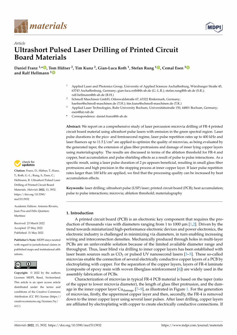
Characterization of microvias in typical FR-4 PCB material is based on the taper (ratioof the upper to lower microvia diameter), the length of glass fiber protrusion, and the dam-age in the inner copper layer Cudamage [7–9], as illustrated in Figure 1. For the generationof microvias, firstly, the uppermost copper layer and then, secondly, the FR-4 is removeddown to the inner copper layer using several laser pulses. After laser drilling, copper layersare affiliated by electroplating with copper to create electrically conductive connections. If
Materials 2022, 15, 3932. https://doi.org/10.3390/ma15113932 https://www.mdpi.com/journal/materials

Materials 2022, 15, 3932 2 of 13
voids are generated during the electroplating, the fatigue life can be significantly reducedby more than 90% [10,11]. For avoiding the generation of voids and to ensure a reliableinterconnection with a high yield between outer and inner copper layers, the aims in lasermicrovia drilling of FR-4 PCB material are:
• Small glass fiber protrusions;• Small taper;• Minimal damage of the inner copper layers;• Small variation of the microvia diameters.
A small variation of the microvia diameters with a high roundness as well as a minimaland uniform damage in the copper inner layer improves the fluid flow characteristics andthus assists the metallization process of microvias. Furthermore, smooth and uniformlysloped sidewalls with small glass fiber protrusions and tapers are easier to metallize,resulting in a higher yield [7].
Limited by the wavelength of the CO2 laser of λ = 9.2–10.6 µm, microvia diameters arerestricted to about 40 µm [12]. In turn, by using nanosecond pulsed lasers with emissionin the ultraviolet (UV) spectral region of λ = 193–355 nm, minimum hole diameters of<25 µm are achieved [3,13–15]. In addition, in this spectral range high absorption ratesare reached for ablation of individual PCB materials such as copper, resin, and glassfiber composite material [16]. Excimer UV lasers are capable of achieving state-of-the-artmicrovia diameters of 20 µm [17] but are also unfavorable due to their high costs [18] andmaintenance of UV optics as well as limited power availability, and additionally requireenhanced safety precautions due to the use of both fluorine and chlorine.
An ultrashort pulse (USP) laser emits laser pulses in the pico- and femtosecondrange [19,20] and is suitable for high-throughput fabrication of micro holes due to highattainable ablation rates and ablation efficiencies [21,22]. The short laser pulse durationslead to so-called cold ablation processes [23,24], which enable a reduction of thermal effectsin laser material processing. Due to small focal diameters and negligible heat input, thedrilling quality can be significantly improved [25–27]. In addition, processing with USPlasers is less dependent on linear absorption properties of different materials, since non-linear absorption mechanisms enable the material removal due to very high pulse peakintensities in the order of 1013 W/cm2 [28,29]. Even in materials that are usually transparentfor the wavelength of the laser, an efficient absorption of light by transferring the valenceband electrons to the conduction band is achievable through non-linear processes suchas multiphoton or tunnel ionization [30]. USP laser beam sources with average powersof several 100 W are nowadays available [31,32], in principle allowing an increase ofproductivity in microvia drilling. The ablation rate is associated to the average power of alaser system (defined by the laser pulse energy and the laser pulse repetition rate [33]) andis currently not inhibited by technology. Rather, the use of higher laser pulse energies andlaser pulse repetition rates is limited by occurring pulse to pulse interaction processes andthe deflection speed of the applied laser scanning system, respectively [33–35].
Figure 1. Laser-based fabrication of microvias in FR-4 PCB material and their technical specificationbased on the taper (ratio of the upper to lower diameter), glass fiber protrusion, and damage in theinner copper layer Cudamage.
Materials 2022, 15, 3932 3 of 13
If laser pulse repetition rates of several hundred kHz are used for percussion drillingof microvias, pulse to pulse interactions must be considered, which have a strong influenceon the precision, productivity, and heat impact in laser material processing [25,36–38]. Theinteraction processes are, in general, distinguished into athermal and thermal processes.An athermal interaction occurs when a laser pulse interacts with laser-induced plasmaor particles induced by a previous laser pulse. As a consequence, incident laser lightcan be absorbed, scattered, or reflected, leading to a shielding effect on the surface of theworkpiece [39–41]. If the time between two consecutive laser pulses is not sufficient todissipate the induced heat into the surrounding volume, thermal interaction processesoccur. In this case, the workpiece is heated up by successive laser pulses, leading to heataccumulation effects [42].
For ultrashort pulsed laser drilling of metals applying laser pulse durations of 0.8–19 ps,Ancona et al. [25,36] show that the effects of particle shielding above 200 kHz is responsiblefor a significant increase in the required number of laser pulses to create a through hole. Inaddition, although the heat accumulation is suitable for shortening the processing time andthus optimizing the process efficiency, negative influences on drilling quality occur due tothe formation of melt. Those findings have also been confirmed by Finger et al. [42] andKononenko et al. [43] using picosecond laser pulses for the investigations of laser percussiondrilling of steel and Ti-based alloy, respectively.
Studying percussion drilling of silicon, Gruner et al. [44] achieved superior processefficiency and drilling quality by using a laser pulse repetition rate of 40 MHz. Heataccumulation was identified as a significant factor enabling efficient material removal anda reduction of the processing time, allowing an effective drilling rate of up to 1000 holesper second. In turn, Döring et al. [45] show that ablated particles within a hole lead toshielding effects that reduce the process efficiency in percussion drilling of silicon. Similarto the results of Ancona et al. [25,36], heat accumulation countervails shielding effects fora laser pulse repetition rate of a few hundred kilohertz. For laser drilling of fused silica,Karimelahi et al. [46] report that an increase of the laser pulse repetition rate in the rangeof 200–1000 kHz leads to less uniform and increasingly damaged drilling channels with alarge heat affected zone (HAZ), located outside the laser focus zone.
Opposite to these fundamental studies on the influence of pulse to pulse interactions inpercussion drilling of metals, dielectrics, and glasses, the athermal and thermal interactionprocesses during the processing of multi-layer materials, such as FR-4 printed circuit boardmaterial, have not yet been adequately investigated. In this study, we therefore analyzethe effects of pulse to pulse interactions on percussion drilling quality of microvias inFR-4 PCB material using different laser pulse durations in the pico- and femtosecondrange, laser pulse repetition rates up to 400 kHz, and laser pulse energies in a range ofE = 15.8–45.8 µJ. For evaluation of the microvia quality, the generated taper, the extensionof glass fiber protrusions and damage of inner lying copper layers of microvias weredetermined by materialography.
2. Materials and Methods2.1. Experimental Setup
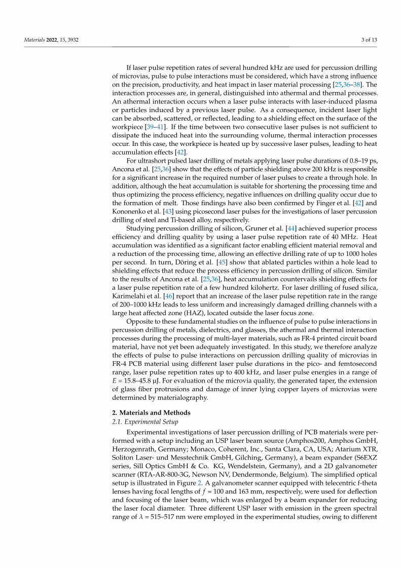
Experimental investigations of laser percussion drilling of PCB materials were per-formed with a setup including an USP laser beam source (Amphos200, Amphos GmbH,Herzogenrath, Germany; Monaco, Coherent, Inc., Santa Clara, CA, USA; Atarium XTR,Soliton Laser- und Messtechnik GmbH, Gilching, Germany), a beam expander (S6EXZseries, Sill Optics GmbH & Co. KG, Wendelstein, Germany), and a 2D galvanometerscanner (RTA-AR-800-3G, Newson NV, Dendermonde, Belgium). The simplified opticalsetup is illustrated in Figure 2. A galvanometer scanner equipped with telecentric f-thetalenses having focal lengths of f = 100 and 163 mm, respectively, were used for deflectionand focusing of the laser beam, which was enlarged by a beam expander for reducingthe laser focal diameter. Three different USP laser with emission in the green spectralrange of λ = 515–517 nm were employed in the experimental studies, owing to different
Materials 2022, 15, 3932 4 of 13
requirements for laser pulse repetition rate, laser pulse energy, laser fluence, and laser pulseduration (specifications listed in Table 1).
Figure 2. Setup for investigations of pulse to pulse interactions in the percussion drilling of microviasin FR-4 PCB material.
Table 1. Technical specification of the ultrashort pulse laser systems and experimental data of theused laser beam configurations for experimental investigations of microvia drilling.
Laser Sources: Laser System 1 Laser System 2 Laser System 3(Amphos 200) (Coherent Monaco) (Atarium XTR)
Technical specifications:Wavelength λ (nm) 1030/515 517 1030/515/343Laser pulse duration τ (ps) 0.9–10 0.23–5 <2Beam quality M2 <1.5 <1.2 <1.3Max. laser power P (W) 200 30 15Max. laser pulse energy E (µJ) 1000 40 300Max. repetition rate f (MHz) 40 0.75 0.5
Experimental data:Raw beam diameter d0 (mm) 5.3 2.8 3.3Focal length of the f-theta lens (mm) 163 100 100Laser focal diameter d f (µm) 30 28 26
Determination of the Influence of different Influence of laser pulseSubject of investigation: ablation thresholds laser pulse durations energy and repetition
of copper and FR-4 on microvia quality rate on microvia quality
For the characterization of the ablation behavior of individual PCB material usingdifferent laser pulse durations of τ = 0.9 and 6 ps and laser fluences of up to 11.5 J/cm2,laser system 1 was used with a focal spot diameter of 30 µm. Using a laser focal spotdiameter of 28 µm, laser system 2 was applied for determining the influence of differentlaser pulse durations of τ = 0.23, 1 and 2 ps on microvia percussion drilling quality. Lasersystem 3 was used to analyze the microvia drilling quality at different laser pulse energiesof E = 15.8–45.8 µJ in combination with laser pulse repetition rates up to 400 kHz using afocal spot diameter of 26 µm.
An overview of the different laser beam configurations for the experimental investi-gations of ultrashort pulsed laser drilling of microvias is pointed out in Table 1. For thedetermination of the laser focal diameter (1/e2), first, the raw beam diameter (1/e2) wasmeasured by a CMOS camera (IDS uEye UI-1490SE) mounted prior to the 2D galvanometerscanner. Afterwards, the laser focal diameter was calculated by substituting the measured
Materials 2022, 15, 3932 5 of 13
raw beam diameter and the experimental data in Equation (1), where f is the focal length, λis the wavelength of the laser, M2 defines the beam quality, and d0 is the raw beam diameter.
d f =4 · f · λ · M2
d0 · π. (1)
2.2. Microvia Characterization
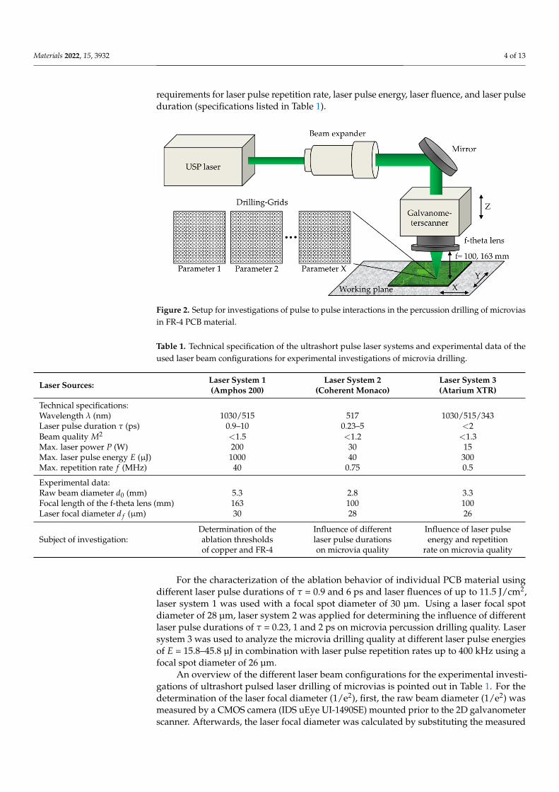
In this study, top and bottom diameter Dtop,bottom, the length of glass fiber protrusionand the damage of the inner copper layer Cudamage were inspected by materialography, asdepicted in Figures 1 and 3a. For the determination of the microvia diameters, top viewimages were evaluated using optical microscopy, cf. Figure 3b. The taper is defined bythe ratio of the microvia top to the bottom diameter, whereby a reference taper of 125%is used for the evaluation of the microvia drilling results. This taper is between classes Aand B of taper specification for microvias [47] and is suitable for High Density Interconnect(HDI) PCBs. The glass fiber protrusion lengths are specified with a maximum of 10%with respect to the microvia diameter, since larger protrusions increase the void formationduring electroplating process with copper [8].
Figure 3. Evaluation of the microvia quality after laser percussion drilling process using (a) materi-alography and (b) optical microscopy.
2.3. Materialographic Preparation and PCB Material
For the determination of the ablation thresholds of individual PCB materials, microholes were drilled into pure copper and FR-4 material using a number of laser pulsesbetween 15–30 (FR-4) and 30–60 (copper), laser pulse durations of τ = 0.9 and 6 ps, andlaser fluences between F = 1.3–11.5 J/cm2. Furthermore, for analyzing the influences ofpulse to pulse interactions in microvia percussion drilling, microvia drilling grids weregenerated in FR-4 PCB material as depicted in Figure 2 using different laser pulse durationsof τ = 0.23, 1 and 2 ps, laser pulse repetition rates of f = 5–400 kHz, laser pulse energies ofE = 15.8–45.8 µJ, and laser fluences between F = 1.4 and 4 J/cm2.
In order to evaluate the quality of laser drilled microvias, the individual drilling gridswere laser cut out of the FR-4 PCB material. After laser cutting process, first, top viewimages were generated using an optical microscope (Leica DM6000 M) to determine thediameter of the microvias, cf. Figure 3b. Afterwards, the cut-out samples were embeddedwith a 2-component synthetic material based on modified polyester resin (Demotec 15 plus)for materialographic preparation. Finally, the hardened material was removed with agrinding and polishing machine (Latzke LS3V) to examine the glass fiber protrusion length,taper, and damage in the inner copper layer in the cross section using optical microscopy,as depicted in Figure 3a.
The studied FR-4 PCB material consists of a 25 µm thick glass/epoxy compositematerial that separates a 5 µm and 16 µm outer and inner copper layer, respectively.
Materials 2022, 15, 3932 6 of 13
3. Results and Discussion3.1. Ablation Thresholds
The ablation thresholds of multi-material PCB were determined by the so-called Liumethod [48], which can be applied for pulsed laser radiation using a Gaussian intensitydistribution for metals and dielectrics [49]. The determination of the specific materialablation threshold requires the radius of ablation r at different laser fluences. The laserfluence is defined by
F =EA
=E
w20 · π
(2)
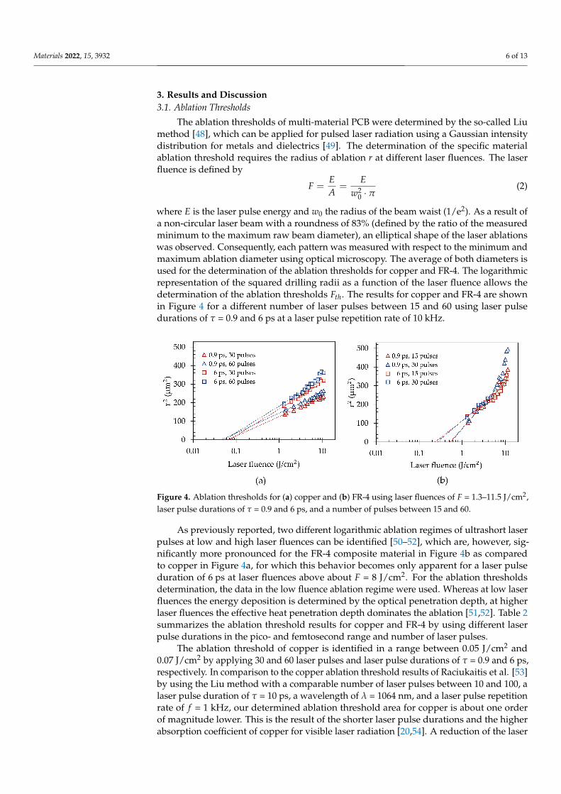
where E is the laser pulse energy and w0 the radius of the beam waist (1/e2). As a result ofa non-circular laser beam with a roundness of 83% (defined by the ratio of the measuredminimum to the maximum raw beam diameter), an elliptical shape of the laser ablationswas observed. Consequently, each pattern was measured with respect to the minimum andmaximum ablation diameter using optical microscopy. The average of both diameters isused for the determination of the ablation thresholds for copper and FR-4. The logarithmicrepresentation of the squared drilling radii as a function of the laser fluence allows thedetermination of the ablation thresholds Fth. The results for copper and FR-4 are shownin Figure 4 for a different number of laser pulses between 15 and 60 using laser pulsedurations of τ = 0.9 and 6 ps at a laser pulse repetition rate of 10 kHz.
Figure 4. Ablation thresholds for (a) copper and (b) FR-4 using laser fluences of F = 1.3–11.5 J/cm2,laser pulse durations of τ = 0.9 and 6 ps, and a number of pulses between 15 and 60.
As previously reported, two different logarithmic ablation regimes of ultrashort laserpulses at low and high laser fluences can be identified [50–52], which are, however, sig-nificantly more pronounced for the FR-4 composite material in Figure 4b as comparedto copper in Figure 4a, for which this behavior becomes only apparent for a laser pulseduration of 6 ps at laser fluences above about F = 8 J/cm2. For the ablation thresholdsdetermination, the data in the low fluence ablation regime were used. Whereas at low laserfluences the energy deposition is determined by the optical penetration depth, at higherlaser fluences the effective heat penetration depth dominates the ablation [51,52]. Table 2summarizes the ablation threshold results for copper and FR-4 by using different laserpulse durations in the pico- and femtosecond range and number of laser pulses.
The ablation threshold of copper is identified in a range between 0.05 J/cm2 and0.07 J/cm2 by applying 30 and 60 laser pulses and laser pulse durations of τ = 0.9 and 6 ps,respectively. In comparison to the copper ablation threshold results of Raciukaitis et al. [53]by using the Liu method with a comparable number of laser pulses between 10 and 100, alaser pulse duration of τ = 10 ps, a wavelength of λ = 1064 nm, and a laser pulse repetitionrate of f = 1 kHz, our determined ablation threshold area for copper is about one orderof magnitude lower. This is the result of the shorter laser pulse durations and the higherabsorption coefficient of copper for visible laser radiation [20,54]. A reduction of the laser
Materials 2022, 15, 3932 7 of 13
pulse duration to τ = 0.9 ps does not cause a significant reduction of the ablation threshold,which is not consistent with the findings of Furusawa et al. [51], observing a reduction ofthe ablation threshold by decreasing the laser pulse duration in a range of τ = 0.12–0.8 psfor a central wavelength of λ = 780 nm. Please note, Furusawa et al. used a differentmethod [27,52] to calculate the ablation threshold for applied laser fluences of F > 1 J/cm2.In addition, shorter laser pulse durations in the femtosecond range as well as a longerwavelength were applied in their experimental investigations.
Table 2. Ablation threshold results for FR-4 composite material and copper at different laser pulsedurations and number of applied laser pulses.
Material Laser PulseDuration (ps)
Number of LaserPulses
Ablation Threshold(J/cm2)
FR-4 composite material
0.9 15 0.5230 0.55
6 15 0.2330 0.26
Copper
0.9 30 0.0660 0.07
6 30 0.0560 0.05
The ablation threshold of FR-4 composite material is determined in a range ofFth = 0.52–0.55 J/cm2 for applying 15 and 30 laser pulses and a laser pulse durationof τ = 0.9 ps, whereas for τ = 6 ps it is about Fth = 0.23–0.26 J/cm2. Additionally, theablation process of FR-4 composite material requires a significantly higher laser fluence ascompared to copper due to different absorption and ablation mechanisms in metals anddielectrics [55].
In conclusion, a remarkable disparity in the ablation threshold of individual multi-layer PCB materials is observed, whereby the ablation process of copper starts at a laserfluence about 9.4 times lower as compared to FR-4. This poses challenges in high through-put microvia drilling of composite materials such as a PCB with potentially suboptimalconditions for the drilling process and a deleterious heat affected zone (HAZ). As the latteris also affected by the laser pulse duration [56], the influence of the laser pulse duration onthe drilling quality is studied next.
3.2. Influence of the Laser Pulse Duration
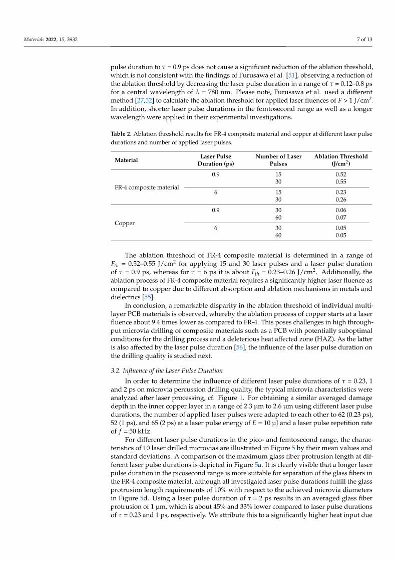
In order to determine the influence of different laser pulse durations of τ = 0.23, 1and 2 ps on microvia percussion drilling quality, the typical microvia characteristics wereanalyzed after laser processing, cf. Figure 1. For obtaining a similar averaged damagedepth in the inner copper layer in a range of 2.3 µm to 2.6 µm using different laser pulsedurations, the number of applied laser pulses were adapted to each other to 62 (0.23 ps),52 (1 ps), and 65 (2 ps) at a laser pulse energy of E = 10 µJ and a laser pulse repetition rateof f = 50 kHz.
For different laser pulse durations in the pico- and femtosecond range, the charac-teristics of 10 laser drilled microvias are illustrated in Figure 5 by their mean values andstandard deviations. A comparison of the maximum glass fiber protrusion length at dif-ferent laser pulse durations is depicted in Figure 5a. It is clearly visible that a longer laserpulse duration in the picosecond range is more suitable for separation of the glass fibers inthe FR-4 composite material, although all investigated laser pulse durations fulfill the glassprotrusion length requirements of 10% with respect to the achieved microvia diametersin Figure 5d. Using a laser pulse duration of τ = 2 ps results in an averaged glass fiberprotrusion of 1 µm, which is about 45% and 33% lower compared to laser pulse durationsof τ = 0.23 and 1 ps, respectively. We attribute this to a significantly higher heat input due
Materials 2022, 15, 3932 8 of 13
to the longer pulse-material interaction, which causes melting of the glass fibers, resultingin smaller glass fiber protrusions.
Figure 5. (a) Glass fiber protrusion, (b) taper, (c) damage in inner copper layer and (d) diameter of10 laser drilled microvias in FR-4 PCB material depending on the laser pulse duration of τ = 0.23,1 and 2 ps using a laser pulse repetition rate of f = 50 kHz, a laser pulse energy of E = 10 µJ and anumber of laser pulses between 52 and 65.
The resulting taper are nearly constant at an averaged level of about 183.3% witha standard deviation of 9.5% by applying laser pulse durations of τ = 0.23 and 1 ps. Incomparison to this, a longer laser pulse duration of 2 ps results in a 19.8% higher taper onaverage, cf. Figure 5b. All in all, in this laser parameter regime the achieved taper does notfulfill the requirements of taper <125% and thus are not suitable for HDI technology inprinted circuit board fabrication.
The evaluation of the damage depths in the inner lying copper layer by using differentlaser pulse durations of τ = 0.23, 1, and 2 ps in combination with a number of laser pulsesbetween 52 and 65 is illustrated in Figure 5c. It is clearly visible that the required stoppingprocess on the inner copper layer can be performed most accurately with the longest laserpulse duration of τ = 2 ps. Here, the standard deviation of 0.22 µm is about half as largeas compared to the other laser pulse durations at a comparable copper damage depth.Though the thermo physical conditions leading to a more precise stopping process at theinner copper layer using a laser pulse duration of 2 ps remain complex, it can be generallyassigned to a combination of a lower pulse peak intensity of the picosecond laser pulses ata constant laser pulse energy, a higher heat input due to the longer laser pulse duration ascompared to femtosecond pulses, and heat dissipation in the plane of the copper layer.
In addition, the microvia diameter increases in an averaged range of 28.6 µm to31 µm, applying a longer laser pulse duration in the picosecond range, which is shownin Figure 5d. Here, the microvia diameter increases by an average of 2.4 µm as comparedto τ = 0.23 ps. Furthermore, the lowest standard deviation of the microvia diameters of0.16 µm is achieved by using femtosecond laser pulses. In comparison to a laser pulseduration of τ = 1 and 2 ps, the standard deviations of the microvia diameters increases by285.2% and 74.5%, respectively.
Materials 2022, 15, 3932 9 of 13
3.3. Influence of the Laser Pulse Energy and Repetition Rate
In ultrashort pulsed laser percussion drilling of microvias, pulse to pulse interactionsmust be taken into account using high laser pulse repetition rates and laser pulse energiesas they can affect laser process efficiency as well as drilling quality, and thus influence thereliability and yield of microvias. For the determination of the influence of athermal andthermal interaction processes on microvia drilling quality, high laser pulse repetition ratesof up to 400 kHz in combination with different laser fluences in a range of F = 1.4–4 J/cm2
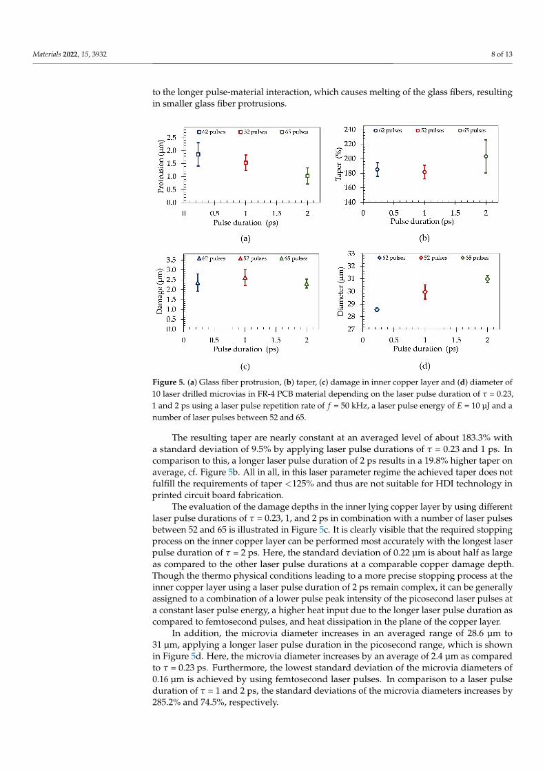
were applied for microvia fabrication in FR-4 PCB material.The characteristics of laser drilled microvias are shown in Figure 6 in dependence of
the number of laser pulses between 27 to 62, a laser pulse repetition rate of f = 5–400 kHz,a laser pulse energy of E = 15.8, 30.8, and 45.8 µJ, and consequently a laser fluence of F = 1.4,2.7 and 4 J/cm2. Please note, the data shown consist of the averaged values of 10 measuredmicrovias and their standard deviations. For laser repetition rates above f = 200 kHz, glassfiber protrusion lengths decrease, which can be assigned to heat accumulation withinthe microvia, and which in turn results from the low heat diffusivity in FR-4 of about0.002 cm2/s [57]. This promotes heating up the material within an area defined by the laserspot diameter over a period of about 10 µs [58], melting glass fibers and epoxy material tosmooth, and cleaning the walls inside the microvias.
Figure 6. (a) Glass fiber protrusion, (b) taper, (c) damage in inner copper layer, and (d) diameter of10 laser drilled microvias depending on the laser pulse energy of E = 15.8–45.8 µJ and laser pulserepetition rate of f = 5–400 kHz using a laser pulse duration of τ = 2 ps.
Heat accumulation also positively influences the occurring taper for higher laser pulserepetition rates and laser fluences of F = 1.4–2.7 J/cm2, cf. Figure 6b, reaching a level of141.8–124.6% for laser pulse repetition rates of f ≥ 200 kHz by melting and broadeningthe bottom of the microvia. This fulfills the typical requirements for the taper geometryand is therefore suitable for HDI technology in PCB manufacturing. It is noteworthy,that for the highest applied laser fluence of F = 4 J/cm2, the taper does not reach thelowest values. This can be attributed to the significantly increased top diameter of themicrovias, as shown in Figure 6d for laser pulse repetition rates of f > 20 kHz. This, again,is ascribed to heat accumulation due to a limited thermal conductivity out of the process
Materials 2022, 15, 3932 10 of 13
zone and an increasing absorption of the copper surface for a higher laser fluence [59] andtemperature [60], further reducing the ablation threshold of copper.
The depth of the inner copper layer damage, as depicted in Figure 6c, decreases withan increasing laser pulse repetition rate due to laser-induced plasma and particle shield-ing effects, once the inner lying copper layer is ablated inside the microvia. This can beevaluated by considering the overall energy input required to successfully drill one compa-rable microvia as a result of the applied number of laser pulses and the laser pulse energy.Employing a laser pulse energy of 15.8 µJ for ultrashort pulsed laser microvia drilling, atotal energy input of 979.6 µJ was required, whereas for a laser pulse energy of 30.8 µJand 45.8 µJ an overall energy input of 1293.6 µJ and 1236.6 µJ were necessary, respectively.Consequently, an increase of the required total energy for drilling one individual microviaby up to 32% is observed for laser fluences of F > 1.4 J/cm2
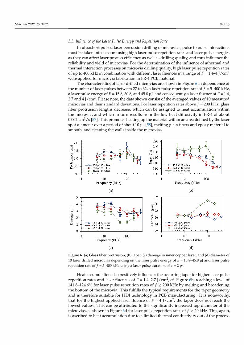
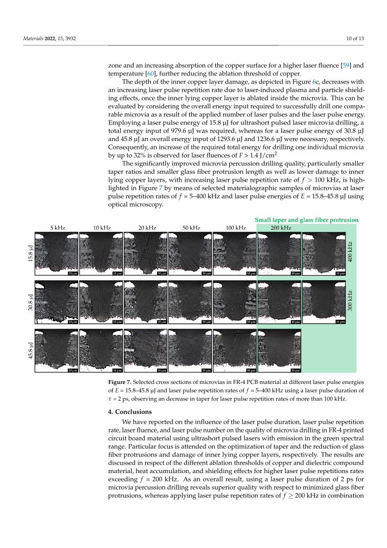
The significantly improved microvia percussion drilling quality, particularly smallertaper ratios and smaller glass fiber protrusion length as well as lower damage to innerlying copper layers, with increasing laser pulse repetition rate of f > 100 kHz, is high-lighted in Figure 7 by means of selected materialographic samples of microvias at laserpulse repetition rates of f = 5–400 kHz and laser pulse energies of E = 15.8–45.8 µJ usingoptical microscopy.
Figure 7. Selected cross sections of microvias in FR-4 PCB material at different laser pulse energiesof E = 15.8–45.8 µJ and laser pulse repetition rates of f = 5–400 kHz using a laser pulse duration ofτ = 2 ps, observing an decrease in taper for laser pulse repetition rates of more than 100 kHz.
4. Conclusions
We have reported on the influence of the laser pulse duration, laser pulse repetitionrate, laser fluence, and laser pulse number on the quality of microvia drilling in FR-4 printedcircuit board material using ultrashort pulsed lasers with emission in the green spectralrange. Particular focus is attended on the optimization of taper and the reduction of glassfiber protrusions and damage of inner lying copper layers, respectively. The results arediscussed in respect of the different ablation thresholds of copper and dielectric compoundmaterial, heat accumulation, and shielding effects for higher laser pulse repetitions ratesexceeding f = 200 kHz. As an overall result, using a laser pulse duration of 2 ps formicrovia percussion drilling reveals superior quality with respect to minimized glass fiberprotrusions, whereas applying laser pulse repetition rates of f ≥ 200 kHz in combination

Materials 2022, 15, 3932 11 of 13
with laser fluences in a range of F = 1.4–2.7 J/cm2 lead to a minimum taper of 124.6%,fulfilling typical requirements for HDI technology in PCB manufacturing.
Author Contributions: Conceptualization, D.F., T.K., G.-L.R., S.R. and R.H.; methodology, D.F.,T.H., T.K., G.-L.R. and S.R.; validation, D.F., T.H., T.K., G.-L.R., S.R. and R.H.; formal analysis, D.F.;investigation, D.F.; data curation, D.F.; writing—original draft preparation, D.F., T.H., G.-L.R., C.E.and R.H.; writing—review and editing, D.F. and R.H.; visualization, D.F.; supervision, C.E. andR.H.; project administration, R.H.; funding acquisition, R.H. All authors have read and agreed to thepublished version of the manuscript.
Funding: This research was funded by the Free State of Bavaria thru project “LEZ@THAB” (fundingnumber H.2-F1116.AS/34/2) and the DFG project ultrashort pulsed lasers (grant 671/39-1).
Conflicts of Interest: The authors declare no conflict of interest.
References1. Hasan, M.; Zhao, J.; Jiang, Z. A review of modern advancements in micro drilling techniques. J. Manuf. Process. 2017, 29, 343–375.
[CrossRef]2. Blank, T. Functional Layers in Printed Circuit Board Development of Intelligent Micro Vibration Sensors in Multidimensional
Printed Circuit Board Technology. Ph.D. Thesis, Karlsruher Institut für Technologie, Karlsruhe, Germany, 2013. (Engl. Translation)3. Liu, F.; Zhang, R.; Khurana, G.; DeProspo, B.H.; Nair, C.; Tummala, R.R.; Swaminathan, M. Smaller microvias for packaging
interconnects by picosecond UV laser with a nanometer metal barrier layer: A feasibility study. IEEE Trans. Compon. Packag. 2020,10, 1411–1418. [CrossRef]
4. Suzuki, Y.; Snyder, E.; Ji, C.; Walther, S.; Gupta, A.; Gottschalk, C.; Sundaram, V.; Tummala, R.R. Microvia formation in 5-µm-thickdry-film dielectric by ozone etch processes. IEEE Trans. Compon. Packag. 2017, 7, 2073–2078.
5. Matsumoto, H.; Unrath, M.; Zhang, H.; Hainsey, B. Laser direct ablation for patterning printed wiring boards using ultrafastlasers and high speed beam delivery architectures. J. Laser Micro Nanoeng. 2013, 8, 315–320. [CrossRef]
6. Sanapala, R.; Sood, B.; Das, D.; Pecht, M. Effect of lead-free soldering on key material properties of FR-4 printed circuit boardlaminates. IEEE Trans. Compon. Packag. 2009, 32, 272–280. [CrossRef]
7. Lei, W.; Davignon, J. Solid state UV laser technology for electronic packaging applications. Lasers Manuf. Mater. Process. 2005,5629, 314–326.
8. Lee, D. Picosecond IR pulsed laser drilling of copper-coated glass/epoxy composite. IEEE Trans. Compon. Packag. 2017, 7,2066–2072. [CrossRef]
9. Yang, C.; Hu, H.; Zhang, H. Modeling AOD-driven laser microvia drilling with machine learning approaches. J. Manuf. Process.2018, 34, 555–565. [CrossRef]
10. Ning, Y.; Azarian, M.H.; Pecht, M. Effects of voiding on thermomechanical reliability of copper-filled microvias: Modeling andsimulation. IEEE Trans. Device Mater. Reliab. 2015, 15, 500–510. [CrossRef]
11. Ning, Y.; Azarian, M.H.; Pecht, M. Influence of plating quality on reliability of microvias. In Proceedings of the IPC APEX EXPOConference, San Diego, CA, USA, 24–26 February 2015.
12. Watanabe, A.O.; Ito, H.; Markondeya, R.P.; Tummala, R.R.; Swaminathan, M. Low-loss impedance-matched sub-25- µm vias in3-D millimeter-wave packages. IEEE Trans. Compon. Packag. 2011, 10, 870–877.
13. Müller, D.; Brune, J.; Pätzel, R. Structuring redistribution layers down to 2 micron line spacing with laser direct ablation. InProceedings of the China Semiconductor Technology International Conference, Shanghai, China, 11–12 March 2018; pp. 1–3.
14. Hollman, R.; Dimov, O.; Malik, S.; Hichri, H.; Arendt, M. Ultra fine RDL structure fabrication using alternative patterning andbottum-up plating processes. In Proceedings of the Electronic Components and Technology Conference, San Diego, CA, USA, 29May–1 June 2018; pp. 58–63.
15. Yamanaka, K.; Kobayashi, K.; Hayashi, K.; Fukui, M. Materials, processes, and performance of high-wiring density buildupsubstrate with ultralow-coefficient of thermal expansion. IEEE Trans. Compon. Packag. 2009, 33, 453–461. [CrossRef]
16. Stafford, S. Printed circuit board processing with UV lasers. Ind.-Lasers 2014, 29, 2.17. Liu, F.; Khurana, G.; Zhang, R.; Watanabe, A.O.; DeProspo, B.H.; Nair, C.; Tummala, R.R. Innovative sub-5-µm microvias by
picosecond UV laser for post-moore packaging interconnects. IEEE Trans. Compon. Packag. 2019, 9, 2016–2023.18. Patel, R.; Bovatsek, J.; Chui, H. Nano to pico to femto: Pulse widths for optimal laser micromachining outcomes. Ind. Laser Solut.
Manuf. 2017, 32, 21–24.19. Ostendorf, A.; Kamlage, G.; Klug, U.; Korte, F.; Chichkov, B.N. Femtosecond versus picosecond laser ablation. In Proceedings of
the Photon Processing in Microelectronics and Photonics IV, San Diego, CA, USA, 12 April 2005; The International Society forOptics and Photonics: Bellingham, WA, USA, 2005; Volume 5713, pp. 1–8.
20. Zhao, W.; Wang, L. Microdrilling of through-holes in flexible printed circuits using picosecond ultrashort pulse laser. Polymers2018, 10, 1390. [CrossRef] [PubMed]
21. Lutz, C.; Roth, G.-L.; Rung, S.; Esen, C.; Hellmann, R. Efficient ultrashort pulsed laser processing by dynamic spatial lightmodulator beam shaping for industrial use. J. Laser Micro Nanoeng. 2016, 21. [CrossRef]

Materials 2022, 15, 3932 12 of 13
22. Schwarz, S.; Rung, S.; Esen, C.; Hellmann R. Enhanced ablation efficiency using GHz bursts in micromachining fused silica. Opt.Lett. 2021, 46, 282–285. [CrossRef] [PubMed]
23. Hohlfeld, J.; Wellershoff, S.S.; Güdde, J.; Conrad, U.; Jähnke, V.; Matthias, E. Electron and lattice dynamics following opticalexcitation of metals. Chem. Phys. 2000, 251, 237–258. [CrossRef]
24. Wellershoff, S.S.; Hohlfeld, J.; Güdde, J.; Matthias, E. The role of electron-phonon coupling in femtosecond laser damage of metals.Appl. Phys. A 1999, 69, 99–107.
25. Ancona, A.; Döring, S.; Jauregui, C.; Röser, F.; Limpert, J.; Nolte, S.; Tünnermann, A. Femtosecond and picosecond laser drillingof metals at high repetition rates and average powers. Opt. Lett. 2009, 34, 3304–3306. [CrossRef]
26. Liu, X.; Du, D.; Mourou, G. Laser ablation and micromachining with ultrashort laser pulses. IEEE J. Quantum Electron. 1997, 33,1706–1716. [CrossRef]
27. Chichkov, B.N.; Momma, C.; Nolte, S.; von Alvensleben, F.; Tünnermann, A. Femtosecond, picosecond and nanosecond laserablation of solids. Appl. Phys. A 1996, 63, 109–115. [CrossRef]
28. Roth, G.-L.; Rung, S.; Hellmann, R. Ultrashort pulse laser micro-welding of cyclo-olefin copolymers. Opt. Lasers Eng. 2017, 93,178–181. [CrossRef]
29. Sima, F.; Sugioka, K.; Vázquez, R.M.; Osellame, R.; Kelemen, L.; Ormos, P. Three-dimensional femtosecond laser processing forlab-on-a-chip applications. Nanophotonics 2018, 7, 613–634. [CrossRef]
30. Sugioka, K.; Cheng, Y. Ultrafast lasers-reliable tools for advanced materials processing. Light Sci. Appl. 2014, 3, e149. [CrossRef]31. Negel, J.-P.; Voss, A.; Ahmed, M.A.; Bauer, D.; Sutter, D.; Killi, A.; Graf, T. 1.1 kW average output power from a thin-disk multipass
amplifier for ultrashort laser pulses. Opt. Lett. 2013, 38, 5442–5445. [CrossRef]32. Russbueldt, P.; Mans, T.; Weitenberg, J.; Hoffmann, H.D.; Poprawe, R. Compact diode-pumped 1.1 kW Yb: YAG Innoslab
femtosecond amplifier. Opt. Lett. 2010, 35, 4169–4171. [CrossRef] [PubMed]33. Finger, J.T. Pulse to Pulse Interactions during Ultrashort Pulse Laser Ablation with High Repetition Rates. Ph.D. Thesis, RWTH
Aachen University, Aachen, Germany, 2017. (Engl. Translation)34. Neuenschwander, B.; Jaeggi, B.; Schmidt, M.; Hennig, G. Surface structuring with ultra-short laser pulses: Basics, limitations and
needs for high throughput. Phys. Procedia 2014, 56, 1047–1058. [CrossRef]35. Römer, G.R.B.E.; Bechtold, P. Electro-optic and acousto-optic laser beam scanners. Phys. Procedia 2014, 56, 29–39. [CrossRef]36. Ancona, A.; Röser, F.; Rademaker, K.; Limpert, J.; Nolte, S.; Tünnermann, A. High speed laser drilling of metals using a high
repetition rate, high average power ultrafast fiber CPA system. Opt. Express 2008, 16, 8958–8968. [CrossRef]37. Breitling, D.; Ruf, A.; Dausinger, F. Fundamental aspects in machining of metals with short and ultrashort laser pulses. In
Proceedings of the Photon Processing in Microelectronics and Photonics III, San Jose, CA, USA, 26–29 January 2004; TheInternational Society for Optics and Photonics: Bellingham, WA, USA, 2004; Volume 5339, pp. 49–63.
38. Finger, J.; Weinand, M.; Wortmann, D. Investigations on processing of carbon fiber reinforced plastics using ultrashort pulsedlaser radiation with high average power. In Proceedings of the ICALEO, Miami, FL, USA, 6–10 October 2013.
39. Föhl, C. Application of Ultrashort Pulsed Laser Radiation for Precision Drilling of Metals. Ph.D. Thesis, Universität Stuttgart,Stuttgart, Germany, 2011. (Engl. Translation)
40. Hertweck, S.M. Temporal Pulse Shaping in Laser Micromaterial Processing: Basic Investigations and Applications. Ph.D. Thesis,Friedrich-Alexander-Universität Erlangen-Nürnberg, Erlangen, Germany, 2017; (Engl. Translation)
41. Hördemann, C. Particle-Free Ablation of Layer Systems for Solid-State Batteries by Means of Ultrashort Pulsed Laser Processing.Ph.D. Thesis, RWTH Aachen University, Aachen, Germany, 2018. (Engl. Translation)
42. Finger, J.; Reininghaus, M. Effect of pulse to pulse interactions on ultrashort pulse laser drilling of steel with repetition rates up to10 MHz. Opt. Express 2014, 22, 18790–18799. [CrossRef] [PubMed]
43. Kononenko, T.V.; Freitag, C.; Sovyk, D.N.; Lukhter, A.B.; Skvortsov, K.V.; Konov, V.I. Influence of pulse repetition rate onpercussion drilling of Ti-based alloy by picosecond laser pulses. Opt. Lasers Eng. 2018, 103, 65–70. [CrossRef]
44. Gruner, A.; Naumann, L.; Schille, J.; Löschner, U. High pulse repetition frequency micro hole drilling of silicon using ultrashortpulse laser radiation. J. Laser Micro Nanoeng. 2019, 14, 190–197.
45. Döring, S.; Ullsperger, T.; Heisler, F.; Richter, S.; Tünnermann, A.; Nolte, S. Hole formation process in ultrashort pulse laserpercussion drilling. Phys. Procedia 2013, 41, 431–440. [CrossRef]
46. Karimelahi, S.; Abolghasemi, L.; Herman, P.R. Rapid micromachining of high aspect ratio holes in fused silica glass by highrepetition rate picosecond laser. Appl. Phys. A 2014, 114, 91–111. [CrossRef]
47. Holden, H. 35 years of HDI fabrication processes and obstacles for implementation. The PCB Magazine, November 2017; pp. 12–24.48. Liu, J.M. Simple technique for measurements of pulsed Gaussian-beam spot sizes. Opt. Lett. 1982, 7, 196–198. [CrossRef]49. Zhou, B.; Kar, A.; Soileau, M.J.; Yu, X. Invariance of the r2-ln (F) relationship and attainable precision in ultrafast laser ablation
experiments. Opt. Express 2021, 29, 5635–5643. [CrossRef]50. Mannion, P.; Magee, J.; Coyne, E.; O’Connor, G.M. Ablation thresholds in ultrafast laser micromachining of common metals in air.
In Proceedings of the Opto-Ireland 2002: Optics and Photonics Technologies and Applications, Galway, Ireland, 5–6 September2003; The International Society for Optics and Photonics: Bellingham, WA, USA, 2003; Volume 4876, pp. 470–478.
51. Furusawa, K.; Takahashi, K.; Kumagai, H.; Midorikawa, K.; Obara, M. Ablation characteristics of Au, Ag, and Cu metals using afemtosecond Ti: Sapphire laser. Appl. Phys. A 1999, 69, 359–366. [CrossRef]
Materials 2022, 15, 3932 13 of 13
52. Nolte, S.; Momma, C.; Jacobs, H.; Tünnermann, A.; Chichkov, B.N.; Wellegehausen, B.; Welling, H. Ablation of metals byultrashort laser pulses. JOSA B 1997, 14, 2716–2722. [CrossRef]
53. Raciukaitis, G.; Brikas, M.; Gecys, P.; Voisiat, B.; Gedvilas, M. Use of high repetition rate and high power lasers in microfabrication:How to keep the efficiency high? J. Laser Micro Nanoeng. 2009, 4, 186–191. [CrossRef]
54. Schille, J.; Schneider, L.; Lickschat, P.; Löschner, U.; Ebert, R.; Exner, H. High-pulse repetition frequency ultrashort pulse laserprocessing of copper. J. Laser Appl. 2015, 4, S28007. [CrossRef]
55. Gamaly, E.G.; Rode, A.V.; Luther-Davies, B.; Tikhonchuk, V.T. Ablation of solids by femtosecond lasers: Ablation mechanism andablation thresholds for metals and dielectrics. Phys. Plasmas 2002, 9, 949–957. [CrossRef]
56. Hodgson, N.; Heming, S.; Steinkopff, A.; Haloui, H.; Lee, T.S. Ultrafast laser ablation at 1035 nm, 517 nm and 345 nm as a functionof pulse duration and fluence. In Proceedings of the Lasers in Manufacturing Conference, Munich, Germany, 24–27 June 2019.
57. Branzei, M.; Vladescu, M. Aspects on thermophisycal properties of interconnection structures for power LEDs applications. InProceedings of the SIITME, Brasov, Romania, 22–25 October 2015.
58. Caulier, O.D.; Mishchik, K.; Chimier, B.; Skupin, S.; Bourgeade, A.; Leger, C.J.; Kling, R.; Hönninger, C.; Lopez, J.; Tikhonchuk,V.; et al. Femtosecond laser pulse train interaction with dielectric materials. Appl. Phys. Lett. 2015, 107, 181110. [CrossRef]
59. Wang, S.Y.; Ren, Y.; Cheng, C.W.; Chen, J.K.; Tzou, D.Y. Micromachining of copper by femtosecond laser pulses. Appl. Surf. Sci.2013, 265, 302–308. [CrossRef]
60. Yeng, Y.; Cheng, J.K.; Zhang, Y. Optical properties and thermal response of copper films induced by ultrashort-pulsed lasers. J.Appl. Phys. 2015, 110, 113102.
Related Documents