Ultrahigh Purcell factor in photonic crystal slab microcavities Lorenzo Sanchis,* Martin J. Cryan, Jose Pozo, Ian J. Craddock, and John G. Rarity Center for Communications Research, Department of Electronic and Electrical Engineering, University of Bristol, Bristol BS8 1UB, United Kingdom Received 2 February 2007; revised manuscript received 18 April 2007; published 30 July 2007 The design of high Purcell factor optical photonic crystal slab microcavities by means of two techniques is presented. First, a combination of stochastic optimization algorithms is used to modify the position of the holes made in a dielectric membrane, breaking their periodic pattern. The combined algorithm is a mixture of a genetic algorithm and a simulated annealing algorithm that is shown to work better than if they were used separately. Secondly, the combined algorithm is used to transform a periodic microcavity where subwavelength sized high-index elements have been inserted. Although the optimization is performed over two dimensional structures with the help of the multiple scattering theory, we show that the optimized microcavities maintain their peculiarities when transformed to their three dimensional equivalent slab microcavities using the finite integration technique. We numerically prove the existence of modified microcavities with extremely small mode volumes of 0.086 91 in / n 3 units and ultrahigh Purcell factor of 75 with an enhancement factor of 5.36 with respect to the unperturbed microcavity. DOI: 10.1103/PhysRevB.76.045118 PACS numbers: 42.70.Qs, 42.82.Et, 42.50.Ct I. INTRODUCTION Photonic crystal PC microcavities with high quality fac- tor Q and small mode volumes V have many important scientific and engineering applications such as high- resolution sensors, 1 low-threshold nanolasers, 2 ultrasmall filters, 3 and efficient single photon sources. 4 The generation of single photons is crucial for practical implementation of quantum cryptography and quantum key distribution 5 as well as linear optics quantum computation. 6 In the future, micro- cavities containing single emitters may also be used for non- linear logic gates in quantum information processing. 7–9 Since three dimensional 3D photonic crystals employing distributed Bragg reflection confinement in 3D have not been perfected yet, two dimensional 2D photonic crystal slabs 10,11 have been proposed as good candidates to support such microcavities. 2D PC microcavities fabricated in a membrane offer many of the benefits of 3D structures with several additional advantages. Due to the easier manufacture by means of present microfabrication and planar techniques, a wide variety of passive and active optical microcavities can be fabricated introducing point or line defects into a periodic array of holes perforating an optically thin semiconductor slab. In these structures, the 2D PC lattice provides in-plane optical confinement, while index guiding is used to achieve confinement in the vertical direction. The use of 2D PC-slab microcavities enables very large Q factors with small effective mode volumes, approaching the theoretical diffraction limit that corresponds to a cubic half wavelength in the material. 12,13 As we will see later, the other important advantage of these structures is the possibility of using much faster 2D modeling tools to describe and design them. The Purcell factor F P of a resonant cavity is a measure of the spontaneous emission rate enhancement of a source placed in the cavity with respect to that in the bulk semicon- ductor. This enhancement leads to an increase in the degree of light-matter interaction for processes such as nonlinear optical responses or coherent electron-photon interactions. The spontaneous emission rate enhancement is useful for ef- ficient pure state single photon sources. The lifetime can be reduced to the point where the photon is effectively time- bandwidth limited, an essential requirement for quantum logic applications. 14 Under some conditions, 15 F P can be written as F P = 3Q/n 3 4 2 V , 1 where Q is the quality factor, n is the refractive index at the location of the maximum squared electric field r max , and is the resonant free space wavelength of the cavity. V is the effective volume of the electromagnetic energy of the reso- nant mode defined as the ratio of the total electric field en- ergy to the peak value of the electric field energy density: V = r E r 2 d 3 r r max E r max 2 . 2 From Eq. 1, we see that there are two ways to increase the Purcell factor. The first one is to increase the cavity qual- ity factor Q, and the second one is to decrease the effective mode volume V. Although until now most methods to maxi- mize the Purcell factor in PC microcavities have been per- formed by modifying the cavity geometry in order to in- crease Q, 3,12,13,16 little progress has been made in creating mechanism for reducing V. In these publications, different procedures are used to reduce the k components within the light cone avoiding out of plane radiation. In some cases, when the cavity’s resonance linewidth is much smaller than the emitter’s for example, with color centers in diamond 17 or rare earth metal doped materials, increasing the cavity Q has no effect on the spontaneous emission. This makes a mode volume reduction necessary instead of trying to find an PHYSICAL REVIEW B 76, 045118 2007 1098-0121/2007/764/04511816 ©2007 The American Physical Society 045118-1

Welcome message from author
This document is posted to help you gain knowledge. Please leave a comment to let me know what you think about it! Share it to your friends and learn new things together.
Transcript
Ultrahigh Purcell factor in photonic crystal slab microcavities
Lorenzo Sanchis,* Martin J. Cryan, Jose Pozo, Ian J. Craddock, and John G. RarityCenter for Communications Research, Department of Electronic and Electrical Engineering, University of Bristol,
Bristol BS8 1UB, United Kingdom�Received 2 February 2007; revised manuscript received 18 April 2007; published 30 July 2007�
The design of high Purcell factor optical photonic crystal slab microcavities by means of two techniques ispresented. First, a combination of stochastic optimization algorithms is used to modify the position of the holesmade in a dielectric membrane, breaking their periodic pattern. The combined algorithm is a mixture of agenetic algorithm and a simulated annealing algorithm that is shown to work better than if they were usedseparately. Secondly, the combined algorithm is used to transform a periodic microcavity where subwavelengthsized high-index elements have been inserted. Although the optimization is performed over two dimensionalstructures with the help of the multiple scattering theory, we show that the optimized microcavities maintaintheir peculiarities when transformed to their three dimensional equivalent slab microcavities using the finiteintegration technique. We numerically prove the existence of modified microcavities with extremely smallmode volumes of 0.086 91 in �� /n�3 units and ultrahigh Purcell factor of 75 with an enhancement factor of5.36 with respect to the unperturbed microcavity.
DOI: 10.1103/PhysRevB.76.045118 PACS number�s�: 42.70.Qs, 42.82.Et, 42.50.Ct
I. INTRODUCTION
Photonic crystal �PC� microcavities with high quality fac-tor �Q� and small mode volumes �V� have many importantscientific and engineering applications such as high-resolution sensors,1 low-threshold nanolasers,2 ultrasmallfilters,3 and efficient single photon sources.4 The generationof single photons is crucial for practical implementation ofquantum cryptography and quantum key distribution5 as wellas linear optics quantum computation.6 In the future, micro-cavities containing single emitters may also be used for non-linear logic gates in quantum information processing.7–9
Since three dimensional �3D� photonic crystals employingdistributed Bragg reflection confinement in 3D have notbeen perfected yet, two dimensional �2D� photonic crystalslabs10,11 have been proposed as good candidates to supportsuch microcavities. 2D PC microcavities fabricated in amembrane offer many of the benefits of 3D structures withseveral additional advantages. Due to the easier manufactureby means of present microfabrication and planar techniques,a wide variety of passive and active optical microcavities canbe fabricated introducing point or line defects into a periodicarray of holes perforating an optically thin semiconductorslab. In these structures, the 2D PC lattice provides in-planeoptical confinement, while index guiding is used to achieveconfinement in the vertical direction.
The use of 2D PC-slab microcavities enables very large Qfactors with small effective mode volumes, approaching thetheoretical diffraction limit that corresponds to a cubic halfwavelength in the material.12,13 As we will see later, the otherimportant advantage of these structures is the possibility ofusing much faster 2D modeling tools to describe and designthem.
The Purcell factor �FP� of a resonant cavity is a measureof the spontaneous emission rate enhancement of a sourceplaced in the cavity with respect to that in the bulk semicon-ductor. This enhancement leads to an increase in the degreeof light-matter interaction for processes such as nonlinear
optical responses or coherent electron-photon interactions.The spontaneous emission rate enhancement is useful for ef-ficient pure state single photon sources. The lifetime can bereduced to the point where the photon is effectively time-bandwidth limited, an essential requirement for quantumlogic applications.14
Under some conditions,15 FP can be written as
FP =3Q��/n�3
4�2V, �1�
where Q is the quality factor, n is the refractive index at thelocation of the maximum squared electric field �r�max�, and �is the resonant free space wavelength of the cavity. V is theeffective volume of the electromagnetic energy of the reso-nant mode defined as the ratio of the total electric field en-ergy to the peak value of the electric field energy density:
V =� ��r���E� �r���2d3r
��r�max��E� �r�max��2. �2�
From Eq. �1�, we see that there are two ways to increasethe Purcell factor. The first one is to increase the cavity qual-ity factor Q, and the second one is to decrease the effectivemode volume V. Although until now most methods to maxi-mize the Purcell factor in PC microcavities have been per-formed by modifying the cavity geometry in order to in-crease Q,3,12,13,16 little progress has been made in creatingmechanism for reducing V. In these publications, differentprocedures are used to reduce the k components within thelight cone avoiding out of plane radiation. In some cases,when the cavity’s resonance linewidth is much smaller thanthe emitter’s �for example, with color centers in diamond17
or rare earth metal doped materials�, increasing the cavity Qhas no effect on the spontaneous emission. This makes amode volume reduction necessary instead of trying to find an
PHYSICAL REVIEW B 76, 045118 �2007�
1098-0121/2007/76�4�/045118�16� ©2007 The American Physical Society045118-1
optimized microcavity with high Q since the Q of the cavityis replaced by the Qm of the material �Qm=�e /��e, where��e is the linewidth of the emitter�.18
Recently, the problem of reducing V of a microcavity hasbeen treated using low-index dielectric discontinuities withsubwavelength dimensions where the high field region islocated.19 The use of dielectric discontinuities has shown thepossibility to confine, enhance, and guide light in a low-refractive-index material as the core in opposition to the con-ventional method of total internal reflection.20 In a high-index contrast interface, to accomplish the continuity of the
normal component of the electric flux density D� , the corre-sponding electric field component must undergo a large dis-continuity with much higher amplitude in the low-index re-gion. This effect, considering Eq. �2�, has been used toefficiently reduce the mode volume in a high-index contrastmicrocavity and achieve high Purcell factors as shown byEq. �1�. In Ref. 19, although high mode volume reduction isachieved, the maximum electric field is situated in the low-index region which is formed by air. However, as the use ofsingle quantum dots as emitters seems to be the most prom-ising option for PC single photon sources,4 the emitter needsto be placed in the semiconductor region instead of the airregion. Thus, it is desirable to have the maximum electricfield of the mode in a substrate where the quantum dot canbe located such as, for example, GaAs. In any event, thisconfiguration may also be attractive in order to maximize theoverlap between an active region and the cavity field whiledesigning a laser cavity or a light-emitting diode.
In this paper, we use two different techniques in order toreduce the mode volume of a 2D periodic PC-slab microcav-ity and we numerically demonstrate that the mode volumereduction produces an enhancement in the Purcell factor. Thefirst technique consists of an appropriate rearrangement ofthe scattering elements of a periodic PC-slab microcavity. Inthis case, the cylindrical holes made in a semiconductor slabare repositioned in order to reduce the mode volume by in-creasing the maximum squared electric field �see Eq. �2��.The second technique to reduce the mode volume consists ofmaking a similar rearrangement of the position of the holesbut this time introducing high-index scattering elements con-fined within the host dielectric medium of the microcavityinspired by the procedure introduced in Ref. 19.
The microcavity analyzed in this paper is modified byemploying an optimization technique consisting of the simul-taneous use of two methods: the genetic algorithm �GA�21
and the simulated annealing �SA�.22 While the binary-codedGA operates on a population of candidate structures to pro-duce new ones with better performance in an iterative pro-cess inspired by Darwinian evolution, SA is an optimizationmethod based on the process of slowly cooling a moltenmetal in order to obtain a uniform crystalline structure. Wedemonstrate that such a combination of optimizing proce-dures gives better performance than the sole use of either ofthem. Although it has been confirmed that GA optimizationis an effective tool in the design of photonic23 or acoustic24
devices based on the modification of periodic photonic oracoustic band gap crystals, little work has been focused onimproving the optimization approach in order to solve a par-
ticular problem. In that direction, we have modified the op-timization strategy in comparison with previous works,where the symmetry was broken by removing some scatter-ing elements from their periodic lattice sites23,24 to accom-plish a specific functionality �focusing an incident beam�. Aswe are dealing with cavities, the final goal is to keep the lightconfined in a region surrounded by the PC. Consequently, itis more efficient to move the scattering elements with respectto their initial periodic locations rather than eliminatingthem. In addition, we have taken into account symmetry con-siderations with the purpose of reducing the space search ofthe optimization process.
In order to apply our GA-SA combined optimization pro-cedure, also called inverse design, the direct problem has tobe solved. Therefore, it is necessary to calculate the electro-magnetic field of a given configuration in a fast and accurateway since it has to be computed several times until conver-gence of the optimization process. To do that, we utilize aself-consistent method named two dimensional multiple scat-tering theory �2D-MST�.25 In essence, the method is basedon analytically solving the boundary conditions related toeach individual scatter in a basis of cylindrical Bessel’s func-tions. Then, the superposition of the waves scattered fromeach object is used to express the total scattered wave. Al-though 2D-MST in conjunction with GA has been success-fully applied in the design of devices formed by clusters ofidentical cylindrical scattering elements,23 in this paper weemploy 2D-MST with clusters formed with a combination ofdifferent kinds of scatters with different dielectric propertiesand radii.
With the aim of saving computing effort, a 2D procedureis used for the optimization. Thus, the microcavities used tosolve the direct problem are formed by arrays of infinitelydeep holes made in an infinitely thick semiconductor slab.Evidently, this configuration is of no use in practice. To en-sure that the real 3D counterparts of the 2D microcavitiesformed by arrays of holes made in finite-thickness semicon-ductor slabs maintain the optimized functionality, it is nec-essary to make full 3D calculations. In that direction, wehave studied the optimized and nonoptimized 2D microcavi-ties created on slabs of three different thickness: 180, 270,and 540 nm. We use the 3D finite integration technique �FIT�method from CST Microwave Studio package31 to analyzethe resulting structures. To the author’s knowledge, the directcomparison between 2D-optimized and 3D counterpart’s be-havior is not yet available in the literature.
II. 2D-MST ANALYSIS OF PC MICROCAVITIES
In this section, we briefly describe the fundamentals of2D-MST which are required to apply the optimization tech-niques used to modify the 2D equivalent of a 3D-slab micro-cavity. This method is well established; however, it is usefulto review it in order to provide sufficient context for theproblem in question. In addition, a decrease of the calcula-tion time required in the optimization procedure is achievedby reducing the computational effort by addressing somenew relations between the elements of the scattering matrix.For a detailed description of this technique, the reader isreferred to Ref. 25 and references therein.
SANCHIS et al. PHYSICAL REVIEW B 76, 045118 �2007�
045118-2
We want to describe the resonant modes of a microcavitymade of an array of infinitely deep cylindrical inclusions in adielectric medium with their symmetry axis parallel to the zaxis in the coordinate system used. The final objective is tocalculate the total scattered wave in the XY plane from adiscrete number of dielectric scatters �with dielectric con-stant �2=1 for holes� placed in a dielectric background char-acterized by �1 for a polarized fixed incident wave and at afixed frequency. The scattered wave will be the mode field ofthe resonant state under proper excitation because the reso-nant mode is a solution of the Maxwell equations in theabsence of any source. The polarization of the incident lightis restricted to TE; hence, the magnetic component of thefield �the only nonzero one� is parallel to the cylinder’s axis.Under this restriction, the full electromagnetic field is com-pletely determined by the z component of the magnetic fieldBz�� and the components of the electric field are Ex= �i /�0�1����� /�y� and Ey = �−i /�0�1����� /�x�. To de-
duce these expressions, the Maxwell equation ��B�
=�0�1�E� /�t has been used; we have considered time depen-
dence e−i�t and taken into account that B� =B�x ,y�u�z. It isimportant to consider that we are dealing with a frequencydomain method as opposed to the FIT method. Let us con-
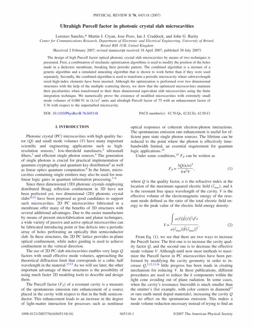
sider an array of N cylinders located at positions R� �=1,2 , . . . ,N� and radius . R� is a vector in the XY planethat defines the position of cylinder . The geometry of theproblem and the variable definitions are shown in Fig. 1.
If an incident wave �inc comes into contact with the array,the total field around the general cylinder � is a superposi-tion of the incident field and the radiation scattered by theremaining cylinders ��,
�� = �inc + ���
N
�scatt, �3�
where �scatt is the field scattered by the cylinder. Those
fields can be expanded as a combination of Bessel functionscentered at the � cylinder position. If the multipole coeffi-cients are �B��l, �S��l, and �A�l, for ��, �
inc, and �scatt,
respectively, the expression above can be cast into the fol-lowing relation between coefficients:
�B��l = �S��l + �=1
N
�l�=−�
l�=�
�G��ll��A�l�, �4�
G� being the propagator from cylinder to � whose com-ponents are
�G��ll� = �1 − ��ei�l�−l���Hl�−l�1� �k1r�� , �5�
where � is the Kronecker delta � �=1 if �=, and �
=1 if ���, Hn�1� is the outgoing Hankel function of order n
and argument k1r� which from now on will be denoted sim-ply as Hn, and k1 is the wave vector in the dielectric medium,k1= �� /c��1. In this particular case, n= l�− l. The propagatorallows the field scattered by cylinder to be expressed in thecoordinate system centered on cylinder � and it is deducedusing Graf’s formula.26
Notice that the coefficients �S��l are known because theydescribe an arbitrary chosen incident field. Our choice wasbased on the fact that these �S��l coefficients should repre-sent a realistic source. Nevertheless, the coefficients �B��l
and �A��l are not known. The boundary conditions of conti-nuity of the field and its derivatives at the surface of the �cylinder relate the coefficients B� and A�, thanks to thesquare and diagonal scattering matrix T� whose elements�t��ll� for TE polarization are
�t��ll� =k2
−1Jl�k1��Jl��k2�� − k1−1Jl��k1��Jl�k2��
k1−1Hl��k1��Jl�k2�� − k2
−1Hl�k1��Jl��k2�� ll�,
�6�
where k1 and k2 are the wave vector numbers in the dielectricregion and in the air region, respectively. Multiplying thesecoefficients by both sides of Eq. �4� and after some simplealgebra, we arrive at
�A��l − �=1
N
�l�=−�
l�=�
�t�G��ll��A�l� = �t�S��l. �7�
By truncating the integers l and l� within �l�� lmax and�l��� lmax, Eq. �7� reduces to a linear system of equations ofdimension N�2lmax+1��N�2lmax+1� that in matrix formreads MA=S. In this equation, A and S are column matriceswith elements A1l ,A2l , . . . ,ANl and t1lS1l , t2lS2l , . . . , tNlSNl, re-spectively. The matrix M can be considered as the scatteringmatrix of the whole set of holes and is a square matrix whereeach element is a submatrix of dimension �2lmax+1�� �2lmax+1�. In short, the matrix elements can be expressedby
�M��ll� = � ll� − �t�G��ll�. �8�
As the matrix M has to be calculated several times, theCPU time required in the calculations can be reduced by halfusing the following relation between the elements of the sub-matrices M� and M�:
�M��ll� = �1 − ���− 1��l�−l��t�ll�
�t��ll�+ ���M��ll�. �9�
�r�
�r�
r�
sourcer�
source
�
�
��r�
Y Axis
X Axis
),( yx�
�� ���
�����
�� ��source��
�R�
�R�
sourceR�
FIG. 1. Coordinate systems and definition of variables employedin the equations of the multiple scattering formalism �see Sec. II�.
ULTRAHIGH PURCELL FACTOR IN PHOTONIC CRYSTAL… PHYSICAL REVIEW B 76, 045118 �2007�
045118-3
This relation is obtained from the properties of the polarvariables ��−��=� and r�=r� �see Fig. 1�. These prop-erties imply that �G��ll�= �−1��l�−l��G��ll�, which when in-troduced into Eq. �8� gives the identity in Eq. �9�.
Although the resonant modes studied here are solutions ofthe system with no source, to obtain the coefficients �A��l itis necessary to properly excite these modes at the resonantfrequency. The incident field is determined by the coeffi-cients �S��l which describe the excitation wave on the systemof coordinates of cylinder �.
��inc = �
l=−lmax
l=lmax
�S��lJl�k1r��eil��. �10�
Let us suppose that we expand the incident field centeredat the origin of coordinates as
�inc = �s=−lmax
s=lmax
�S0�sJs�k1r�eils�. �11�
Now, it is necessary to express the coefficients of the ex-citation field centered at the origin of coordinates �S0�s in thesystem of coordinates of cylinder �. To do so, Graf’s formulais used once more.
�inc = �s=−lmax
s=lmax
�S0�sJs�k1r�eils�
= �s=−lmax
s=lmax
�S0�s �l=−lmax
l=lmax
ei�s−l���Js−l�k1R��Jl�k1r��eil��
= �l=−lmax
l=lmax
�S��lJl�k1r��eil��, �12�
where the coefficients �S��l are
�S��l = �s=−lmax
s=lmax
�S0�sei�s−l���Js−l�k1R�� . �13�
In the following, we will use 2D magnetic point sourcesas excitation elements. Considering TE polarization, a 2Dmagnetic point source is an oscillating current along the z
direction at position R� source= �xsource ,ysource� represented by a
Hankel function of order zero. �inc=H0�k1�r�−R� source�� thatcentered at the origin using Graf’s formula is
�inc = H0�k1�r� − R� source��
= �s=−lmax
s=lmax
e−is�sourceH−s�k1Rsource�Js�k1r�eis�. �14�
Comparing Eqs. �14� and �11�, we get the coefficients thatdescribe the incident field as a function of the position of thesource,
�S0�s = e−is�sourceH−s�k1Rsource� . �15�
Finally, the unknown coefficients of the column matrix Acan be obtained by matrix inversion. The field of the reso-nant mode on the dielectric region is the sum of the scatteredfields of all the cylinders:
�mode�x,y� = ��=1
N
�l=−lmax
l=lmax
�A��lHl�k1r��eil��. �16�
With the preceding formalism, we are able to determinethe mode profile in the high-index region for a given fre-quency. Notice that an equivalent procedure is possible inorder to obtain the field inside the holes. Nevertheless, as itwill be shown in Secs. IV and V, for the structure to bestudied with the use of the proposed optimization algorithm,it is not necessary to know the field in the low-index regions�holes�. For the sake of simplicity and to perform faster cal-culations, we have set these values equal to zero. Once the2D-optimized microcavity is obtained, the whole field profilewill be calculated in 3D space �holes inclusive� with the FITmethod in order to deduce the microcavity Purcell factorwhich we wish to enhance. Finally, this Purcell factor will becompared with that of a periodic nonoptimized microcavity.
III. UNPERTURBED MICROCAVITY
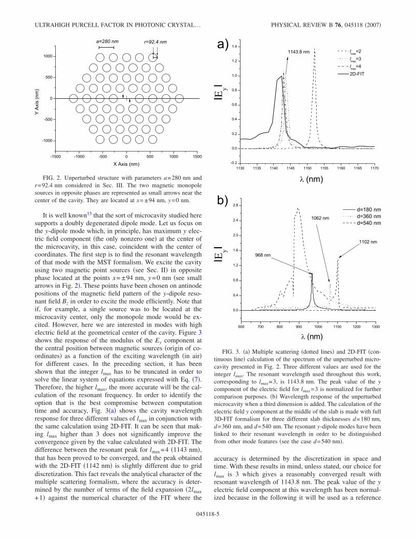
In this paper, we will start from an unperturbed microcav-ity using GA-SA optimization to improve its performance.More specifically, we will enhance its Purcell factor by thereduction of the mode volume while, at the same time, main-taining or eventually increasing the value of Q. It is thereforecrucial to know the characteristics of the original or unper-turbed microcavity to compare with the ones obtained withthe optimization strategies that we will use. Also, it is essen-tial to know how these characteristics are transformed whenan additional dimension is added; passing from a 2D micro-cavity to its 3D counterpart, for example, we will see a shiftin the resonant frequency. The motivation for this is thatwhile we are finally interested in a 3D structure, the optimi-zation process will be done under 2D constraints. Therefore,our goal is to achieve a relative enhancement of the Purcellfactor between the 3D optimized microcavity, the counterpartof the 2D-optimized one, and the 3D unperturbed one. First,the 2D unperturbed microcavity will be studied with the helpof MST and FIT, and then, the 3D case will be consideredusing FIT.
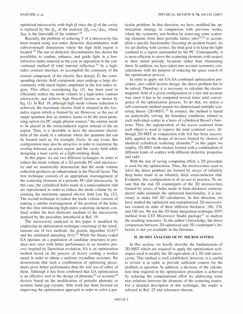
The periodic unperturbed single-defect 2D microcavitytreated in this section �see Fig. 2� consists of a missing holein a hexagonal array of holes ��2=1, or n2=1� made in aninfinite-thickness slab of GaAs ��1=12.6, or n1=3.55�. Thedefect region is surrounded by four layers of holes with lat-tice constant a=280 nm and radius r=0.33a=92.4 nm. Wewant to stress that such reduced number of holes is deter-mined by our computational resources given that, for theoptimization process, the mode field must be calculated sev-eral times. It is important to remember the fact that we areinterested in the relative improvement of the Purcell factorbetween an unperturbed and a perturbed microcavity to vali-date our method and promote its use in future work. There-fore, the inclusion of additional holes will not help us in ourpurpose.
SANCHIS et al. PHYSICAL REVIEW B 76, 045118 �2007�
045118-4
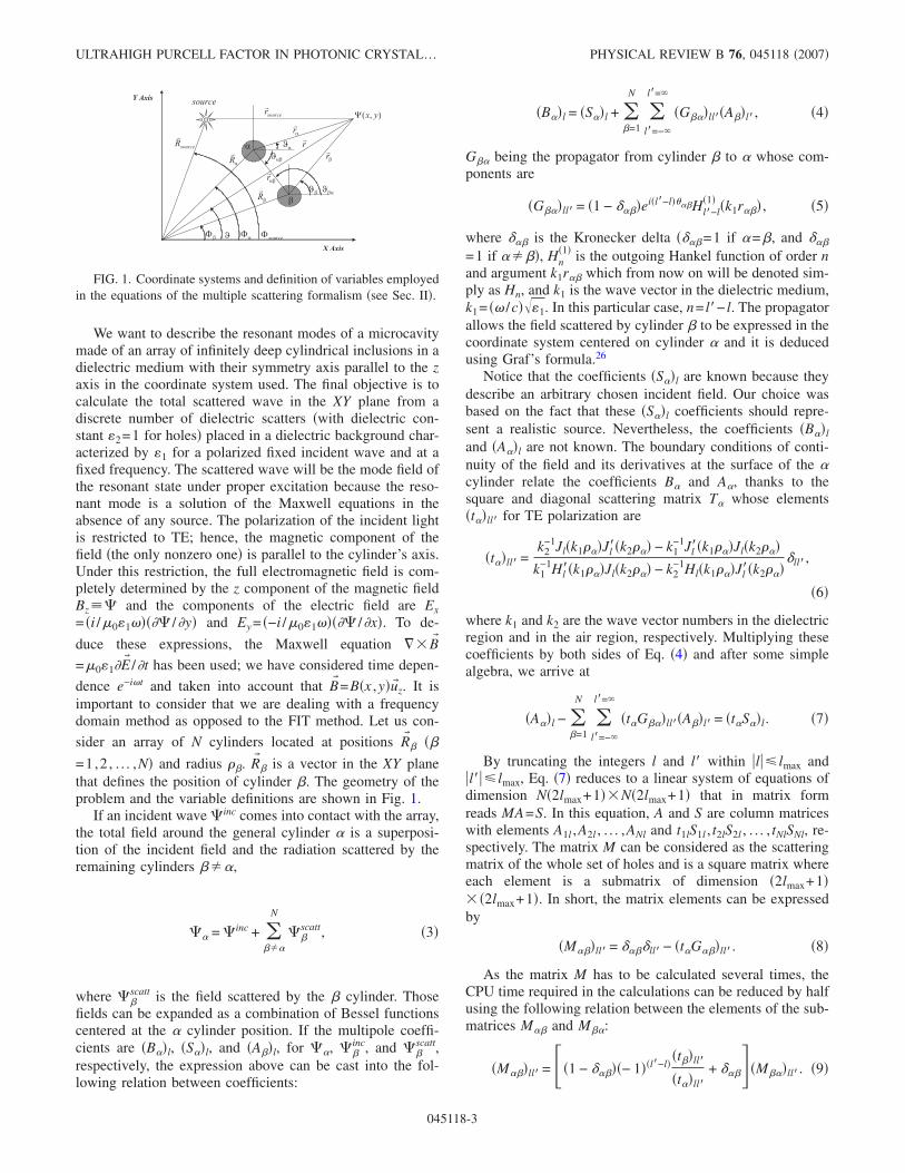
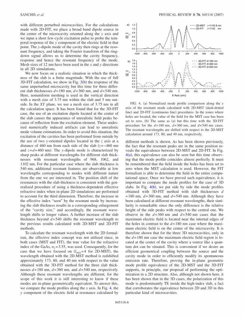
It is well known13 that the sort of microcavity studied heresupports a doubly degenerated dipole mode. Let us focus onthe y-dipole mode which, in principle, has maximum y elec-tric field component �the only nonzero one� at the center ofthe microcavity, in this case, coincident with the center ofcoordinates. The first step is to find the resonant wavelengthof that mode with the MST formalism. We excite the cavityusing two magnetic point sources �see Sec. II� in oppositephase located at the points x= ±94 nm, y=0 nm �see smallarrows in Fig. 2�. These points have been chosen on antinodepositions of the magnetic field pattern of the y-dipole reso-nant field Bz in order to excite the mode efficiently. Note thatif, for example, a single source was to be located at themicrocavity center, only the monopole mode would be ex-cited. However, here we are interested in modes with highelectric field at the geometrical center of the cavity. Figure 3shows the response of the modulus of the Ey component atthe central position between magnetic sources �origin of co-ordinates� as a function of the exciting wavelength �in air�for different cases. In the preceding section, it has beenshown that the integer lmax has to be truncated in order tosolve the linear system of equations expressed with Eq. �7�.Therefore, the higher lmax, the more accurate will be the cal-culation of the resonant frequency. In order to identify theoption that is the best compromise between computationtime and accuracy, Fig. 3�a� shows the cavity wavelengthresponse for three different values of lmax in conjunction withthe same calculation using 2D-FIT. It can be seen that mak-ing lmax higher than 3 does not significantly improve theconvergence given by the value calculated with 2D-FIT. Thedifference between the resonant peak for lmax=4 �1143 nm�,that has been proved to be converged, and the peak obtainedwith the 2D-FIT �1142 nm� is slightly different due to griddiscretization. This fact reveals the analytical character of themultiple scattering formalism, where the accuracy is deter-mined by the number of terms of the field expansion �2lmax
+1� against the numerical character of the FIT where the
accuracy is determined by the discretization in space andtime. With these results in mind, unless stated, our choice forlmax is 3 which gives a reasonably converged result withresonant wavelength of 1143.8 nm. The peak value of the yelectric field component at this wavelength has been normal-ized because in the following it will be used as a reference
FIG. 2. Unperturbed structure with parameters a=280 nm andr=92.4 nm considered in Sec. III. The two magnetic monopolesources in opposite phases are represented as small arrows near thecenter of the cavity. They are located at x= ±94 nm, y=0 nm.
FIG. 3. �a� Multiple scattering �dotted lines� and 2D-FIT �con-tinuous line� calculation of the spectrum of the unperturbed micro-cavity presented in Fig. 2. Three different values are used for theinteger lmax. The resonant wavelength used throughout this work,corresponding to lmax=3, is 1143.8 nm. The peak value of the ycomponent of the electric field for lmax=3 is normalized for furthercomparison purposes. �b� Wavelength response of the unperturbedmicrocavity when a third dimension is added. The calculation of theelectric field y component at the middle of the slab is made with full3D-FIT formalism for three different slab thicknesses d=180 nm,d=360 nm, and d=540 nm. The resonant y-dipole modes have beenlinked to their resonant wavelength in order to be distinguishedfrom other mode features �see the case d=540 nm�.
ULTRAHIGH PURCELL FACTOR IN PHOTONIC CRYSTAL… PHYSICAL REVIEW B 76, 045118 �2007�
045118-5
with different perturbed microcavities. For the calculationsmade with 2D-FIT, we place a broad band dipole source inthe center of the microcavity oriented along the y axis andwe input a short few-cycle excitation pulse to probe the tem-poral response of the y component of the electric field in thatpoint. The y-dipole mode of the cavity then rings at the reso-nant frequency, and taking the Fourier transform of the ring-down signal allows us to determine the cavity frequency,response and hence the resonant frequency of the mode.Mesh sizes of 12 nm have been used in the x and y directionsin all 2D simulations.
We now focus on a realistic situation in which the thick-ness of the slab is a finite magnitude. With the use of full3D-FIT calculation, we show in Fig. 3�b� the response of thesame unperturbed microcavity but this time for three differ-ent slab thicknesses d=180 nm, d=360 nm, and d=540 nm.Here, nonuniform meshing is used in the vertical directionwith a mesh size of 3.75 nm within the slab and 5 nm out-side. In the XY plane, we use a mesh size of 3.75 nm in allthe calculation space. It has been found that for the 3D-FITcase, the use of an excitation dipole located at the center ofthe slab causes the appearance of unrealistic field peaks be-cause of reflection from the excitation element. These undes-ired numerically induced artifacts can lead to unrealisticmode volume estimations. In order to avoid this situation, theexcitation of the cavities has been performed from outside bythe use of two y-oriented dipoles located in the z axis at adistance of 460 nm from each side of the slab �z=−460 nmand z=d+460 nm�. The y-dipole mode is characterized bysharp peaks at different wavelengths for different slab thick-nesses with resonant wavelengths of 968, 1062, and1102 nm. For the particular case where the slab thickness is540 nm, additional resonant features are observable at lowwavelengths corresponding to modes with different naturefrom the one we are interested in. The position shift of theresonances with the slab thickness is consistent with the gen-eralized procedure of using a thickness-dependent effectiverefractive index when in-plane 2D simulations are performedto account for the third dimension. Therefore, the increase inthe effective index “seen” by the resonant mode by increas-ing the slab thickness results in a corresponding enlargementof the “cavity size,” and accordingly, the resonant wave-length shifts to longer values. A further increase of the slabthickness beyond d=540 shifts the resonant wavelength tothe previous results calculated with 2D-MST and 2D-FITmethods.
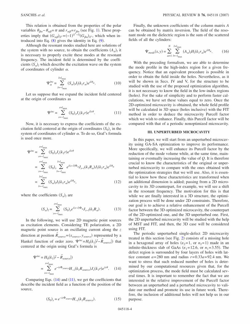
To calculate the resonant wavelength with the 2D formal-ism, the effective index concept was not utilized since, inboth cases �MST and FIT�, the true value for the refractiveindex of the GaAs, n1=3.55, was used. Consequently, for thecase that we have focused on �lmax=4 for 2D-MST�, thewavelength obtained with the 2D-MST method is redshiftedapproximately 173, 80, and 40 nm with respect to the valueobtained with the 3D-FIT method for the three slab thick-nesses d=180 nm, d=360 nm, and d=540 nm, respectively.Although these resonant wavelengths are different, for thescope of this work it is still interesting to know if thesemodes are in-plane geometrically equivalent. To answer this,we compare the mode profiles along the x axis. In Fig. 4, they component of the electric field at resonance calculated by
different methods is shown. As has been shown previously,the fact that the resonant peaks are in the same position re-veals the equivalence between 2D-MST and 2D-FIT. In Fig.4�a�, this equivalence can also be seen but this time observ-ing that the mode profile coincides almost perfectly. It mustbe remembered that the field inside the holes has been set tozero when the MST calculation is used. However, the FITformalism is able to determine the field in the entire compu-tational space. Once we have proved such equivalence, it isimportant to compare the mode profiles for the case of 3Dslabs. In Fig. 4�b�, we put side by side the mode profilesobtained with 3D-FIT method with slab thicknesses d=180 nm, d=360 nm, and d=540 nm. Although they havebeen calculated at different resonant wavelengths, their simi-larity is remarkable since the only difference is the relativeheight of the side peaks with respect to the central one. Weobserve in the d=360 nm and d=540 nm cases that themaximum electric field is located near the internal edges ofthe holes in contrast to the d=180 nm case where the maxi-mum electric field is on the center of the microcavity. It istherefore shown that for the three 3D microcavities, only inthe d=180 nm case the maximum electric field region is lo-cated at the center of the cavity where a source like a quan-tum dot can be situated. This is convenient if we desire anefficient geometrical coupling between the source and thecavity mode in order to efficiently modify its spontaneousemission rate. Therefore, proving the in-plane geometricmode profile equivalence of the 2D-MST and the 3D-FITsupports, in principle, our proposal of performing the opti-mization in a 2D structure. Also, although not shown here, ithas been shown that in the 3D cases, the polarization of thismode is predominantly TE inside the high-index slab, a factthat corroborates the equivalence between 2D and 3D in thisparticular kind of microcavities.
FIG. 4. �a� Normalized mode profile comparison along the xaxis of the resonant mode calculated with 2D-MST �dash-dottedline� and 2D-FIT �continuous line� procedures. In the zones whereholes are located, the value of the field for the MST case has beenset to zero. �b� The same as �a� but this time with the 3D-FITprocedure for the d=180 nm, d=360 nm, and d=540 nm cases.The resonant wavelengths are shifted with respect to the 2D-MSTcalculation around 173, 80, and 40 nm, respectively.
SANCHIS et al. PHYSICAL REVIEW B 76, 045118 �2007�
045118-6
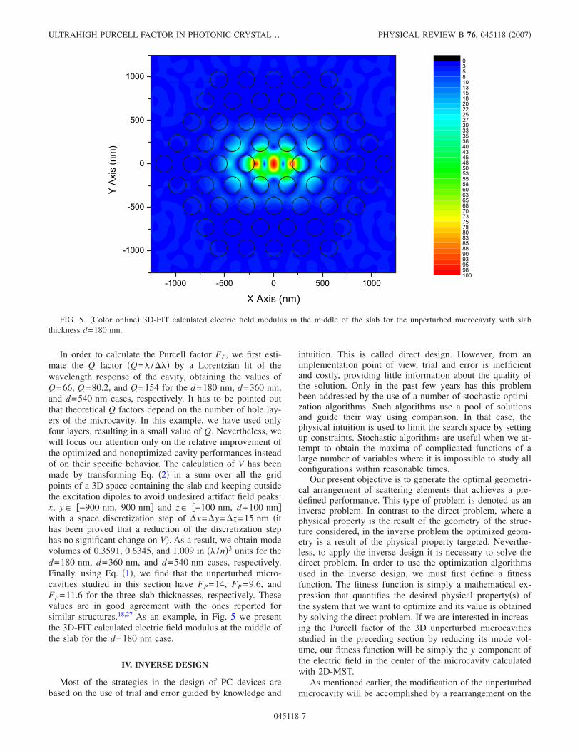
In order to calculate the Purcell factor FP, we first esti-mate the Q factor �Q=� /��� by a Lorentzian fit of thewavelength response of the cavity, obtaining the values ofQ=66, Q=80.2, and Q=154 for the d=180 nm, d=360 nm,and d=540 nm cases, respectively. It has to be pointed outthat theoretical Q factors depend on the number of hole lay-ers of the microcavity. In this example, we have used onlyfour layers, resulting in a small value of Q. Nevertheless, wewill focus our attention only on the relative improvement ofthe optimized and nonoptimized cavity performances insteadof on their specific behavior. The calculation of V has beenmade by transforming Eq. �2� in a sum over all the gridpoints of a 3D space containing the slab and keeping outsidethe excitation dipoles to avoid undesired artifact field peaks:x, y� �−900 nm, 900 nm� and z� �−100 nm, d+100 nm�with a space discretization step of �x=�y=�z=15 nm �ithas been proved that a reduction of the discretization stephas no significant change on V�. As a result, we obtain modevolumes of 0.3591, 0.6345, and 1.009 in �� /n�3 units for thed=180 nm, d=360 nm, and d=540 nm cases, respectively.Finally, using Eq. �1�, we find that the unperturbed micro-cavities studied in this section have FP=14, FP=9.6, andFP=11.6 for the three slab thicknesses, respectively. Thesevalues are in good agreement with the ones reported forsimilar structures.18,27 As an example, in Fig. 5 we presentthe 3D-FIT calculated electric field modulus at the middle ofthe slab for the d=180 nm case.
IV. INVERSE DESIGN
Most of the strategies in the design of PC devices arebased on the use of trial and error guided by knowledge and
intuition. This is called direct design. However, from animplementation point of view, trial and error is inefficientand costly, providing little information about the quality ofthe solution. Only in the past few years has this problembeen addressed by the use of a number of stochastic optimi-zation algorithms. Such algorithms use a pool of solutionsand guide their way using comparison. In that case, thephysical intuition is used to limit the search space by settingup constraints. Stochastic algorithms are useful when we at-tempt to obtain the maxima of complicated functions of alarge number of variables where it is impossible to study allconfigurations within reasonable times.
Our present objective is to generate the optimal geometri-cal arrangement of scattering elements that achieves a pre-defined performance. This type of problem is denoted as aninverse problem. In contrast to the direct problem, where aphysical property is the result of the geometry of the struc-ture considered, in the inverse problem the optimized geom-etry is a result of the physical property targeted. Neverthe-less, to apply the inverse design it is necessary to solve thedirect problem. In order to use the optimization algorithmsused in the inverse design, we must first define a fitnessfunction. The fitness function is simply a mathematical ex-pression that quantifies the desired physical property�s� ofthe system that we want to optimize and its value is obtainedby solving the direct problem. If we are interested in increas-ing the Purcell factor of the 3D unperturbed microcavitiesstudied in the preceding section by reducing its mode vol-ume, our fitness function will be simply the y component ofthe electric field in the center of the microcavity calculatedwith 2D-MST.
As mentioned earlier, the modification of the unperturbedmicrocavity will be accomplished by a rearrangement on the
FIG. 5. �Color online� 3D-FIT calculated electric field modulus in the middle of the slab for the unperturbed microcavity with slabthickness d=180 nm.
ULTRAHIGH PURCELL FACTOR IN PHOTONIC CRYSTAL… PHYSICAL REVIEW B 76, 045118 �2007�
045118-7
lattice positions of the scattering centers of an initially peri-odic array of cylindrical holes made in an infinitely thickslab of GaAs. We take advantage �see Eq. �2�� of the mirrorsymmetry of the sources with respect to the y axis and thedouble mirror symmetry of the microcavity with respect tothe x and y axes to reduce the space search size. Notice thatsuch characteristics give double mirror symmetry characterto the mode studied in Sec. III with respect to the x and yaxes. Any displacement made over a hole with coordinates x0and y0 with x0�0 and y0�0 has its mirror symmetryequivalent displacement for the three remaining holes withcoordinates �−x0 ,y0�, �x0 ,−y0�, and �−x0 ,−y0�; hence, thedouble mirror symmetry of the mode is maintained. So, al-though the microcavity has 60 scattering elements, thealgorithm-guided position modifications will be done onlyover the 18 ones situated in the first quadrant, letting theremaining ones move according to their respective mirrorsymmetry counterparts. If the mode symmetry is maintained,the electric field peak y component will remain located at thecenter of the microcavity and will continue being the onlynonzero one at this point. Consequently, a direct comparisonwith the unperturbed microcavity can be made. Once wehave used intuition to reduce the search space and, at thesame time, maintain the double mirror symmetry of themode, it is necessary to specify how the holes are moved. Wehave chosen a displacement along the line defined by theorigin of coordinates and the center of each hole. With thatrestriction, the relative position of each hole with respect tothe equilibrium position is defined with a real number reduc-ing even further the search space size. This real number isdefined positive if the hole is moved away from the center ofthe microcavity or negative if is moved toward it. Therefore,we can relate the equilibrium position coordinates x0 and y0of a generic hole with the perturbed ones x and y by thefollowing equations:
x = x0 + Tj cosarctan� y0
x0 � ,
y = y0 + Tj sinarctan� y0
x0 � , �17�
where j is an integer that takes values between j=−7 and j=7 and T is a control parameter measured in nanometerscalled temperature. Its meaning will be explained later inSec. IV B, where the simulated annealing optimization pro-cedure is described.
Once we have set the parameters of the optimizationproblem, we can calculate the search space size, in otherwords, the number of possible configurations of the system.For each hole, there are 15 different positions. Consideringthat we have 18 holes in the first quadrant, for a fixed tem-perature, we obtain 1518�1.4�1021 possibilities. Even us-ing symmetry considerations to reduce the space search size,such a huge number makes a stochastic algorithm indispens-able in tackling the optimization problem. Of course, thenumber of possibilities could be drastically reduced by, forexample, letting j run from −2 to 2. Nevertheless, the quality
of the optimized solution is directly related to the spacesearch size. Again, we have selected these parameters con-sidering our computing capabilities.
The drawback when a stochastic algorithm is used is thatthere is no guarantee that the global optimum has been foundafter the search is completed. In any case, what can certainlybe assumed is that the solution obtained is among the bestand has comparable quality to the global maximum. In thenext sections, three different stochastic algorithms will beused: GA, SA, and a combination of both, namely, GA-SA.Therefore, in order to have an insight on each one’s perfor-mance and be able to compare them, six different runs willbe carried out on each case. The comparison and the resultsshown will be made between the best of the six runs for eachalgorithm.
A. Genetic algorithm
The GA belongs to a family of stochastic search algo-rithms called evolutionary computation, which are com-monly used to solve a wide variety of engineering problems,and recently it has been applied in the field of photonic andphononic crystals.23,24 This assemblage of algorithms is re-lated to the optimization process used by nature itself: evo-lution. Like evolution, GA adapts individuals to a given en-vironment and is by very simple means able to tackle verycomplex optimization problems. The evolution is guidedthrough generations by mixing different individuals’ chromo-somes and new individuals with new modified characteristicsare born, possessing some properties from parents. Thoseindividuals who adapt better to the environment have thebest chance of survival and hence give birth to more off-spring creating a new generation more fit for survival thanthe previous one. Evolutionary computation tries to mimicthe steps taken by nature and uses it as an optimization pro-cess. GA uses a population of individuals to guide the search.The concept of individual is employed to address a specificdesign in the optimization process. Therefore, the populationof individuals is a group of designs. For the specific problemconsidered here, each individual corresponds to a fixed dis-tribution of holes in the XY plane. In GA optimization, theindividual is normally described as a string of binary bitscalled a chromosome and how chromosomes are associatedto each structure is called codification. The chromosome isdivided up into genes, where each gene is related to onespecific hole. Therefore, if each hole can be placed on 15positions, its gene can be represented with a binary string oflength 4 that has 24=16 combinations. Notice that since thenumber of positions is odd, it is impossible to find a binarystring with the same number of possible combinations �for abinary string of length N, there are 2N combinations�. Tosolve this problem, we link two different genes to the equi-librium position. This will have no effect on the optimizationresults since this only slightly increases the search space.Finally, each individual is represented with a chromosomewith a string of 18 genes and a length of 18�4=72 bits. Apossibility would be to choose the simplest codification pos-sible as in Ref. 23. In this work, the length of the genes islimited to one single bit, coding the presence or the absence
SANCHIS et al. PHYSICAL REVIEW B 76, 045118 �2007�
045118-8
of a cylinder at a fixed lattice site. Nevertheless, the aim ofthis work is to construct an efficient resonant cavity so theelimination of any cylinder would lead to a leaky structure.
At that point, to be able to apply GA, each individualneeds to be given a value corresponding to how well thisindividual solves the problem. This is the fitness functionthat in our case is the y component of the electric field on thecenter of the microcavity. GA mimics the evolutionary pro-cess of a population by identifying three different operations,natural selection, the mating act, and genetic mutation whichare called operators selection, crossover, and mutation. First,an initial population of individuals is set randomly to excludeany external guidance. The first operator applied to the popu-lation is selection. Selection culls the population selectingbetter solutions over worse by using a survival of the fittestapproach. The second operator is crossover that directs themating act. This operator takes two chromosomes as input,given by selection, and mixes these two strings to produce anew individual with properties from the two parents. Beforethe new individual is added to the new population, it is modi-fied by the mutation operator. Mutation simply introducessome randomness into the solution, normally with some lowprobability, in order to avoid convergence to a local maxi-
mum. These three operators are repeatedly applied until thenew population has reached the size of the initial one. Theold population is then replaced by the new one, with theexception of the best fitted solution, which automatically iscopied into the new population. This practice is called elit-ism. This process is repeated until convergence and the op-timal solution is found to be the best one of the population.
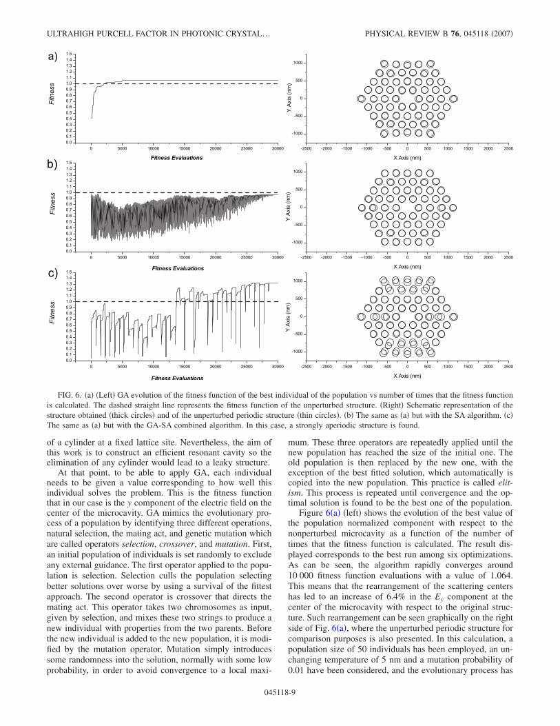
Figure 6�a� �left� shows the evolution of the best value ofthe population normalized component with respect to thenonperturbed microcavity as a function of the number oftimes that the fitness function is calculated. The result dis-played corresponds to the best run among six optimizations.As can be seen, the algorithm rapidly converges around10 000 fitness function evaluations with a value of 1.064.This means that the rearrangement of the scattering centershas led to an increase of 6.4% in the Ey component at thecenter of the microcavity with respect to the original struc-ture. Such rearrangement can be seen graphically on the rightside of Fig. 6�a�, where the unperturbed periodic structure forcomparison purposes is also presented. In this calculation, apopulation size of 50 individuals has been employed, an un-changing temperature of 5 nm and a mutation probability of0.01 have been considered, and the evolutionary process has
FIG. 6. �a� �Left� GA evolution of the fitness function of the best individual of the population vs number of times that the fitness functionis calculated. The dashed straight line represents the fitness function of the unperturbed structure. �Right� Schematic representation of thestructure obtained �thick circles� and of the unperturbed periodic structure �thin circles�. �b� The same as �a� but with the SA algorithm. �c�The same as �a� but with the GA-SA combined algorithm. In this case, a strongly aperiodic structure is found.
ULTRAHIGH PURCELL FACTOR IN PHOTONIC CRYSTAL… PHYSICAL REVIEW B 76, 045118 �2007�
045118-9
been stopped at generation 600. For details about the mean-ing of the optimization parameters, the reader can consultRef. 21. It has to be pointed out that MST formalism is onlyvalid if the cylindrical inclusions do not touch. In order toavoid overlap between adjacent holes, the algorithm givesautomatically a null value to the fitness of the individualswhich have one or more holes overlapped. The algorithmtends to wipe out those individuals, leaving only structures inwhich the MST calculation can be considered accurate. Al-though demonstrating fast convergence, because of the mod-est increment in the y electric field component compared tothe unperturbed microcavity, we can conclude that GA pro-cedure has been proved unsuited to this optimization prob-lem. The reason for this is that the holes are confined aroundinitial equilibrium positions �periodic array of the unper-turbed structure�. With the aim of overcoming this constraint,a different stochastic algorithm is introduced.
B. Simulated annealing
This general optimization method was first introduced byKirkpatrick et al.22 It simulates the softening process �an-nealing� of metal. The metal is heated up to a temperaturenear its melting point and then slowly cooled down. Thispermits the particles to move toward a uniform crystallinestructure with an optimum energy state. SA is a variation ofthe hill-climbing algorithm. The difference between SA andthe hill-climbing algorithm is that if the fitness of a new trialsolution �Ei+1� is less than the fitness of the current solution�Ei�, in SA the trial solution is not automatically rejected, asit is in the hill-climbing algorithm. This trial solution be-comes the current solution with a certain transition probabil-ity p which depends on the difference in fitness �E=Ei+1−Ei and the temperature T. The acceptance of bad transitionstries to avoid getting stuck in a local maximum. Temperatureis an abstract control parameter that here represents the de-gree of similitude with respect to the equilibrium position ofthe holes �see Eq. �17��. The transition probability for a giventemperature and a given difference in fitness is
p = � 1 if Ei+1 � Ei
e�E/T if Ei+1 � Ei.� �18�
The algorithm starts with the equilibrium state of the un-perturbed microcavity and a starting temperature T0. Thisstate has fitness E0=1 corresponding to the normalized ycomponent of the electric field in the center of the cavity.Then, a random structure is generated whose hole positionsare defined by Eq. �17� and its fitness E1 is calculated. Thisstate, according to Eq. �18�, has probability p to become thenew equilibrium state. This annealing step process is re-peated until the temperature takes a null value. The way thetemperature decreases along the cooling process is called thecooling schedule which governs how likely a bad transitionis accepted as a function of time. In the beginning of thesearch, we are interested in using randomness to explore thesearch space widely, so the probability of accepting a nega-tive transition is high. As the search progresses, we seek tolimit transitions to local improvements and optimizations sothe probability of moving from a high-fitness state to a
lower-fitness state is reduced. The cooling schedule is deter-mined by the initial temperature T0 and the temperature dec-rement function. Several decrement functions can be chosenbut a detailed study of this subject is beyond the scope of thiswork. We have selected the simplest one that seems to workproperly28 where the temperature is reduced linearly accord-ing to the formula
Ti = T0 −iT0
N, �19�
where Ti is the temperature of the annealing step i, and N isthe number of annealing steps �i=0, . . . ,N�. In the optimiza-tion example shown in left side of Fig. 6�b�, which corre-sponds to the best result among six runs, one can see theevolution of the fitness function as a function of the numberof times that is calculated. We have used an initial tempera-ture of 0.1 nm and 30 000 annealing steps. The choice of ahigher initial temperature has the consequence of a fast con-vergence to zero of the fitness function due to overlapping ofthe cylinders. Note that the fitness function has been calcu-lated the same number of times as in the GA case �population50 individuals�600 generations� for comparison purposesbetween the optimization methods. The right side of Fig.6�b� illustrates the resulting structure superposed with theinitial unperturbed periodic structure. As it is manifest, thereis no improvement with respect to the periodic structure asthe fitness function is less than 1. The difference with thepreceding case is that whereas the initial state structure isalways the same in GA �the periodic unperturbed microcav-ity�, in SA this state is permitted to change with some prob-ability while the optimization is running. This means that inthe GA case the positions of the holes are constrained tomove around fixed points, while in the SA case the holes canmigrate freely. Surprisingly, although the holes have the pos-sibility to be positioned far away from their initial periodicpositions, the resultant structure almost maintains its periodicoriginal nature. Therefore, the SA method is not suitable ifwe intend to optimize a periodic structure by breaking itsperiodic pattern. The spontaneous emergence of periodic pat-terns in a biological inspired simulation of photonic struc-tures has been recently reported.29
C. Combined GA-SA algorithm
At this point, the optimization of a 2D microcavity usingtwo different stochastic algorithms has been studied. On onehand, the GA optimization, although with fast convergence,leads to a structure whose scattering centers are locatedaround the equilibrium positions of the unperturbed micro-cavity because of a geometrical constraint. On the otherhand, with the SA algorithm, an almost periodic structurewith worse performance is also obtained due to the nature ofthe algorithm. While in the GA case the holes do not havethe possibility to migrate freely from their original periodicpositions, the SA case is not suitable in order to improve theperformance of a periodic microcavity by breaking their pe-riodicity. In this section, we describe a combined GA-SAalgorithm that gathers the advantages of both methods whiletheir drawbacks are eliminated. As previously shown, in the
SANCHIS et al. PHYSICAL REVIEW B 76, 045118 �2007�
045118-10
SA method each repositioning is made randomly and theacceptance of each new configuration depends on a probabil-ity. In the combined GA-SA algorithm, instead of generatingrandomly the new state, it is generated by a GA run. Thus,this algorithm is a sequence of GA runs in which the accep-tance of a transition to an initial GA state is determined bythe same probability as in the SA case. In addition, the tem-perature is gradually decreased in each GA run. We havemade a sequence of 40 annealing steps �GA runs� with aninitial temperature of 5 nm. Each GA run has a populationsize of 15 individuals which evolve over 50 generations andwith mutation probability of 0.01. Figure 6�c� �left� describesthe evolution of the best value of the fitness function of thepopulation as a function of the number of times that it iscalculated. The example shown is the best among six runs ofthe GA-SA combined algorithm. Figure 6�c� �right� showsthe resulting structure and the unperturbed one for compari-son purposes. At the end of the optimization process, a struc-ture with fitness function of 1.323 has been found. Thismeans an increment of the Ey component of 32.3% withrespect to the unperturbed microcavity. The structure ob-tained is rather different from the original periodic one as theholes can move freely over the plane. At this point, it mustbe kept in mind that although the structure is different, it hasthe same resonant wavelength of 1143.8 nm as the originalone since this is the wavelength at which it has been opti-mized �see Sec. III�.
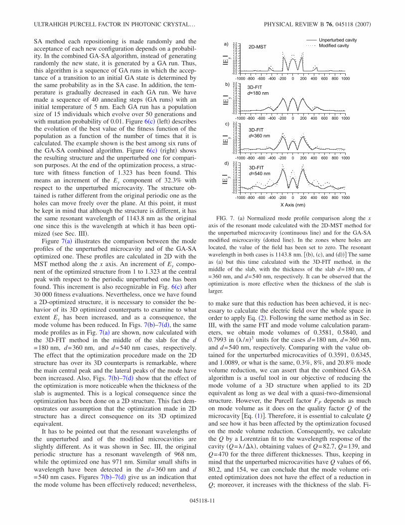
Figure 7�a� illustrates the comparison between the modeprofiles of the unperturbed microcavity and of the GA-SAoptimized one. These profiles are calculated in 2D with theMST method along the x axis. An increment of Ey compo-nent of the optimized structure from 1 to 1.323 at the centralpeak with respect to the periodic unperturbed one has beenfound. This increment is also recognizable in Fig. 6�c� after30 000 fitness evaluations. Nevertheless, once we have founda 2D-optimized structure, it is necessary to consider the be-havior of its 3D optimized counterparts to examine to whatextent Ey has been increased, and as a consequence, themode volume has been reduced. In Figs. 7�b�–7�d�, the samemode profiles as in Fig. 7�a� are shown, now calculated withthe 3D-FIT method in the middle of the slab for the d=180 nm, d=360 nm, and d=540 nm cases, respectively.The effect that the optimization procedure made on the 2Dstructure has over its 3D counterparts is remarkable, wherethe main central peak and the lateral peaks of the mode havebeen increased. Also, Figs. 7�b�–7�d� show that the effect ofthe optimization is more noticeable when the thickness of theslab is augmented. This is a logical consequence since theoptimization has been done on a 2D structure. This fact dem-onstrates our assumption that the optimization made in 2Dstructure has a direct consequence on its 3D optimizedequivalent.
It has to be pointed out that the resonant wavelengths ofthe unperturbed and of the modified microcavities areslightly different. As it was shown in Sec. III, the originalperiodic structure has a resonant wavelength of 968 nm,while the optimized one has 971 nm. Similar small shifts inwavelength have been detected in the d=360 nm and d=540 nm cases. Figures 7�b�–7�d� give us an indication thatthe mode volume has been effectively reduced; nevertheless,
to make sure that this reduction has been achieved, it is nec-essary to calculate the electric field over the whole space inorder to apply Eq. �2�. Following the same method as in Sec.III, with the same FIT and mode volume calculation param-eters, we obtain mode volumes of 0.3581, 0.5840, and0.7993 in �� /n�3 units for the cases d=180 nm, d=360 nm,and d=540 nm, respectively. Comparing with the value ob-tained for the unperturbed microcavities of 0.3591, 0.6345,and 1.0089, or what is the same, 0.3%, 8%, and 20.8% modevolume reduction, we can assert that the combined GA-SAalgorithm is a useful tool in our objective of reducing themode volume of a 3D structure when applied to its 2Dequivalent as long as we deal with a quasi-two-dimensionalstructure. However, the Purcell factor FP depends as muchon mode volume as it does on the quality factor Q of themicrocavity �Eq. �1��. Therefore, it is essential to calculate Qand see how it has been affected by the optimization focusedon the mode volume reduction. Consequently, we calculatethe Q by a Lorentzian fit to the wavelength response of thecavity �Q=� /���, obtaining values of Q=82.7, Q=139, andQ=470 for the three different thicknesses. Thus, keeping inmind that the unperturbed microcavities have Q values of 66,80.2, and 154, we can conclude that the mode volume ori-ented optimization does not have the effect of a reduction inQ; moreover, it increases with the thickness of the slab. Fi-
FIG. 7. �a� Normalized mode profile comparison along the xaxis of the resonant mode calculated with the 2D-MST method forthe unperturbed microcavity �continuous line� and for the GA-SAmodified microcavity �dotted line�. In the zones where holes arelocated, the value of the field has been set to zero. The resonantwavelength in both cases is 1143.8 nm. ��b�, �c�, and �d��� The sameas �a� but this time calculated with the 3D-FIT method, in themiddle of the slab, with the thickness of the slab d=180 nm, d=360 nm, and d=540 nm, respectively. It can be observed that theoptimization is more effective when the thickness of the slab islarger.
ULTRAHIGH PURCELL FACTOR IN PHOTONIC CRYSTAL… PHYSICAL REVIEW B 76, 045118 �2007�
045118-11
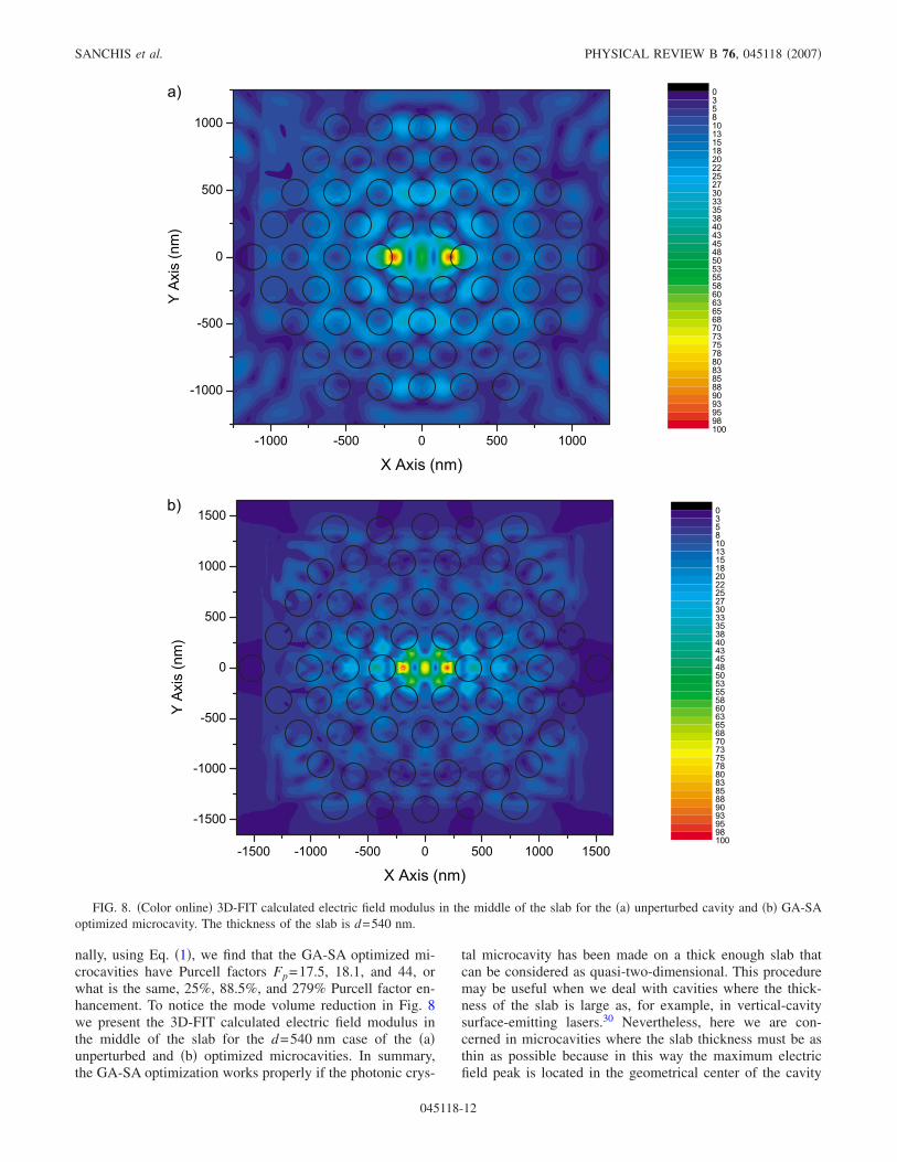
nally, using Eq. �1�, we find that the GA-SA optimized mi-crocavities have Purcell factors Fp=17.5, 18.1, and 44, orwhat is the same, 25%, 88.5%, and 279% Purcell factor en-hancement. To notice the mode volume reduction in Fig. 8we present the 3D-FIT calculated electric field modulus inthe middle of the slab for the d=540 nm case of the �a�unperturbed and �b� optimized microcavities. In summary,the GA-SA optimization works properly if the photonic crys-
tal microcavity has been made on a thick enough slab thatcan be considered as quasi-two-dimensional. This proceduremay be useful when we deal with cavities where the thick-ness of the slab is large as, for example, in vertical-cavitysurface-emitting lasers.30 Nevertheless, here we are con-cerned in microcavities where the slab thickness must be asthin as possible because in this way the maximum electricfield peak is located in the geometrical center of the cavity
FIG. 8. �Color online� 3D-FIT calculated electric field modulus in the middle of the slab for the �a� unperturbed cavity and �b� GA-SAoptimized microcavity. The thickness of the slab is d=540 nm.
SANCHIS et al. PHYSICAL REVIEW B 76, 045118 �2007�
045118-12
�see Fig. 4�b�, d=180 nm case� and it has the smallest modevolume. In the next section, we introduce a different tech-nique that is able to reduce the mode volume of a PC micro-cavity made on a thin slab.
V. OPTIMIZED MICROCAVITY WITH HIGH-INDEXINCLUSIONS
A. Optimization
In the preceding section, we have developed an optimiza-tion method able to reduce the mode volume of a periodicPC microcavity by making an adequate redistribution of thescattering centers. In this section, we introduce high-refractive-index scattering elements in the center of the mi-crocavity with the purpose of finding an even greater reduc-tion in the mode volume. These high-index elements willcause an enhancement of the electric field in the region inbetween them. In contrast to previous work19 where the highfield region was in air, this region will be situated in the bulkGaAs semiconductor where a quantum dot can be grown. Ashigh-index scattering elements, we have used two small cyl-inders of radius 25 nm located at x=0, y=27.5 and x=0, y=−27.5 where the coordinates are expressed in nanometers.With this configuration, we find the y electric field compo-nent of the y-dipole mode perpendicular to the high-indexcylinder interfaces and in the geometrical center of the mi-crocavity.
For the numerical calculations, the dielectric constant ofthe high-index inclusions has been chosen to be 25, greaterthan that of GaAs, 12.6. With these geometric specifications,we are ready to apply the combined GA-SA algorithm. In afirst run, we found that the y electric component rapidly di-verges to very high values due to the fact that the algorithmtends to bring the high-index cylinders together. This is anexpected behavior since the electric field amplitude enhance-ment in the low-index region is increased as the gap widthbetween interfaces decreases.19 The aim of this paper is todesign a microcavity where a quantum dot could be locatedbetween the two high-index elements. Thus, we fix them atoriginal locations, x=0, y=27.5 and x=0, y=−27.5, with aresulting gap width of 5 nm, and disallow their movement.Although this allows for only a small quantum dot, we areusing this as a starting design which can be further modifiedto allow for more realistic quantum dot dimensions. Once thepositions of the small cylinders have been fixed, we applyour GA-SA algorithm to the remaining cylinders to find theoptimized distribution of holes that maximizes the y electricfield component, and thus, as it has been shown, to obtain asmall mode volume microcavity.
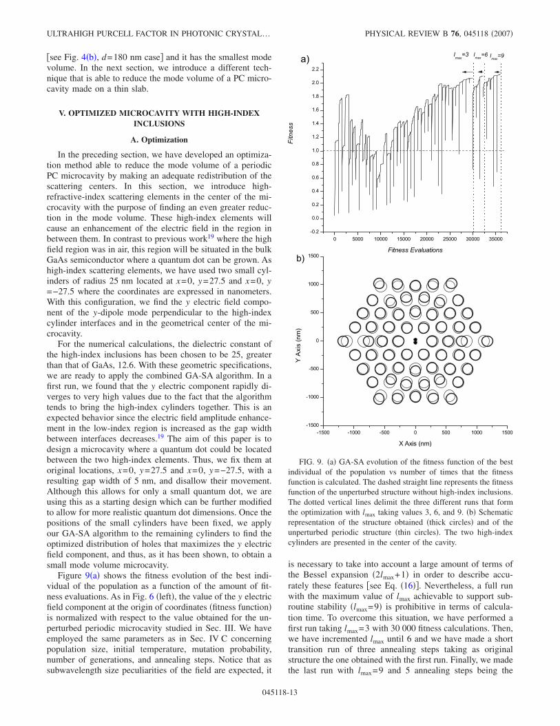
Figure 9�a� shows the fitness evolution of the best indi-vidual of the population as a function of the amount of fit-ness evaluations. As in Fig. 6 �left�, the value of the y electricfield component at the origin of coordinates �fitness function�is normalized with respect to the value obtained for the un-perturbed periodic microcavity studied in Sec. III. We haveemployed the same parameters as in Sec. IV C concerningpopulation size, initial temperature, mutation probability,number of generations, and annealing steps. Notice that assubwavelength size peculiarities of the field are expected, it
is necessary to take into account a large amount of terms ofthe Bessel expansion �2lmax+1� in order to describe accu-rately these features �see Eq. �16��. Nevertheless, a full runwith the maximum value of lmax achievable to support sub-routine stability �lmax=9� is prohibitive in terms of calcula-tion time. To overcome this situation, we have performed afirst run taking lmax=3 with 30 000 fitness calculations. Then,we have incremented lmax until 6 and we have made a shorttransition run of three annealing steps taking as originalstructure the one obtained with the first run. Finally, we madethe last run with lmax=9 and 5 annealing steps being the
FIG. 9. �a� GA-SA evolution of the fitness function of the bestindividual of the population vs number of times that the fitnessfunction is calculated. The dashed straight line represents the fitnessfunction of the unperturbed structure without high-index inclusions.The dotted vertical lines delimit the three different runs that formthe optimization with lmax taking values 3, 6, and 9. �b� Schematicrepresentation of the structure obtained �thick circles� and of theunperturbed periodic structure �thin circles�. The two high-indexcylinders are presented in the center of the cavity.
ULTRAHIGH PURCELL FACTOR IN PHOTONIC CRYSTAL… PHYSICAL REVIEW B 76, 045118 �2007�
045118-13
initial temperature of the three runs 5, 1, and 1 nm, respec-tively. Thus, we ensure accuracy in the solution without thenecessity of carrying out the whole optimization run with alarge value of lmax. The three runs are delimited by verticaldotted lines in Fig. 9�a�. As before, in the optimization pro-cess we have used a wavelength of 1143.8 nm correspondingto the resonant state calculated for the unperturbed structureusing 2D-MST with lmax=3. As a result, we obtain a 2Dmicrocavity where the y electric field component at the cen-ter is 2.1327 times higher than that of the unperturbed 2Dperiodic structure with no high-index inclusions. Figure 9�b�illustrates the hole distribution of both of these structures.
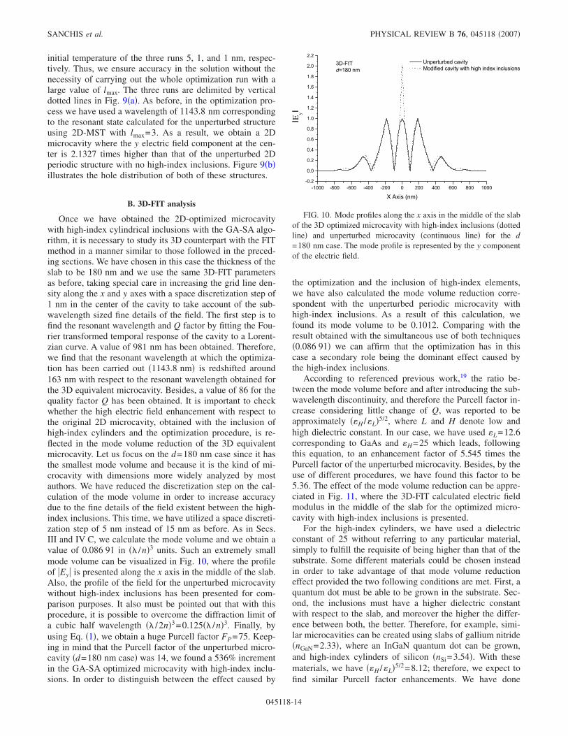
B. 3D-FIT analysis
Once we have obtained the 2D-optimized microcavitywith high-index cylindrical inclusions with the GA-SA algo-rithm, it is necessary to study its 3D counterpart with the FITmethod in a manner similar to those followed in the preced-ing sections. We have chosen in this case the thickness of theslab to be 180 nm and we use the same 3D-FIT parametersas before, taking special care in increasing the grid line den-sity along the x and y axes with a space discretization step of1 nm in the center of the cavity to take account of the sub-wavelength sized fine details of the field. The first step is tofind the resonant wavelength and Q factor by fitting the Fou-rier transformed temporal response of the cavity to a Lorent-zian curve. A value of 981 nm has been obtained. Therefore,we find that the resonant wavelength at which the optimiza-tion has been carried out �1143.8 nm� is redshifted around163 nm with respect to the resonant wavelength obtained forthe 3D equivalent microcavity. Besides, a value of 86 for thequality factor Q has been obtained. It is important to checkwhether the high electric field enhancement with respect tothe original 2D microcavity, obtained with the inclusion ofhigh-index cylinders and the optimization procedure, is re-flected in the mode volume reduction of the 3D equivalentmicrocavity. Let us focus on the d=180 nm case since it hasthe smallest mode volume and because it is the kind of mi-crocavity with dimensions more widely analyzed by mostauthors. We have reduced the discretization step on the cal-culation of the mode volume in order to increase accuracydue to the fine details of the field existent between the high-index inclusions. This time, we have utilized a space discreti-zation step of 5 nm instead of 15 nm as before. As in Secs.III and IV C, we calculate the mode volume and we obtain avalue of 0.086 91 in �� /n�3 units. Such an extremely smallmode volume can be visualized in Fig. 10, where the profileof �Ey� is presented along the x axis in the middle of the slab.Also, the profile of the field for the unperturbed microcavitywithout high-index inclusions has been presented for com-parison purposes. It also must be pointed out that with thisprocedure, it is possible to overcome the diffraction limit ofa cubic half wavelength �� /2n�3=0.125�� /n�3. Finally, byusing Eq. �1�, we obtain a huge Purcell factor FP=75. Keep-ing in mind that the Purcell factor of the unperturbed micro-cavity �d=180 nm case� was 14, we found a 536% incrementin the GA-SA optimized microcavity with high-index inclu-sions. In order to distinguish between the effect caused by
the optimization and the inclusion of high-index elements,we have also calculated the mode volume reduction corre-spondent with the unperturbed periodic microcavity withhigh-index inclusions. As a result of this calculation, wefound its mode volume to be 0.1012. Comparing with theresult obtained with the simultaneous use of both techniques�0.086 91� we can affirm that the optimization has in thiscase a secondary role being the dominant effect caused bythe high-index inclusions.
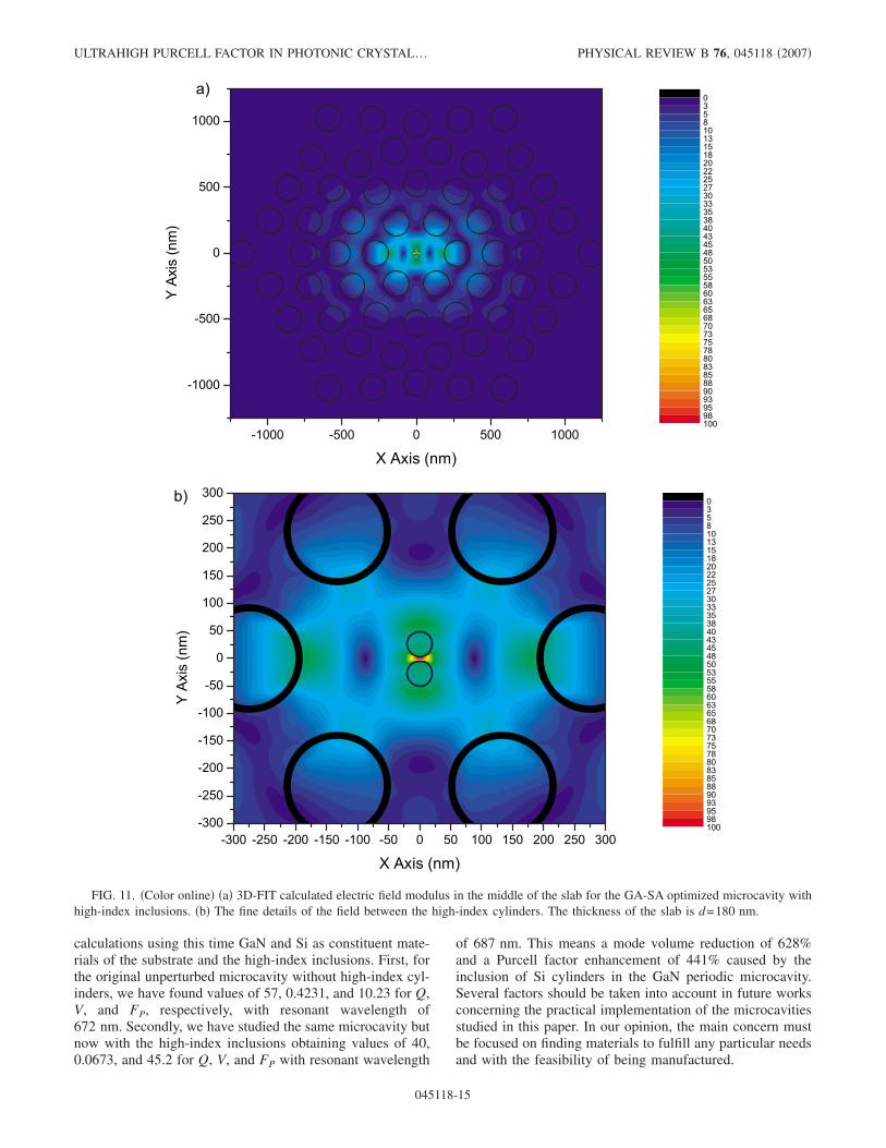
According to referenced previous work,19 the ratio be-tween the mode volume before and after introducing the sub-wavelength discontinuity, and therefore the Purcell factor in-crease considering little change of Q, was reported to beapproximately ��H /�L�5/2, where L and H denote low andhigh dielectric constant. In our case, we have used �L=12.6corresponding to GaAs and �H=25 which leads, followingthis equation, to an enhancement factor of 5.545 times thePurcell factor of the unperturbed microcavity. Besides, by theuse of different procedures, we have found this factor to be5.36. The effect of the mode volume reduction can be appre-ciated in Fig. 11, where the 3D-FIT calculated electric fieldmodulus in the middle of the slab for the optimized micro-cavity with high-index inclusions is presented.
For the high-index cylinders, we have used a dielectricconstant of 25 without referring to any particular material,simply to fulfill the requisite of being higher than that of thesubstrate. Some different materials could be chosen insteadin order to take advantage of that mode volume reductioneffect provided the two following conditions are met. First, aquantum dot must be able to be grown in the substrate. Sec-ond, the inclusions must have a higher dielectric constantwith respect to the slab, and moreover the higher the differ-ence between both, the better. Therefore, for example, simi-lar microcavities can be created using slabs of gallium nitride�nGaN=2.33�, where an InGaN quantum dot can be grown,and high-index cylinders of silicon �nSi=3.54�. With thesematerials, we have ��H /�L�5/2=8.12; therefore, we expect tofind similar Purcell factor enhancements. We have done
FIG. 10. Mode profiles along the x axis in the middle of the slabof the 3D optimized microcavity with high-index inclusions �dottedline� and unperturbed microcavity �continuous line� for the d=180 nm case. The mode profile is represented by the y componentof the electric field.
SANCHIS et al. PHYSICAL REVIEW B 76, 045118 �2007�
045118-14
calculations using this time GaN and Si as constituent mate-rials of the substrate and the high-index inclusions. First, forthe original unperturbed microcavity without high-index cyl-inders, we have found values of 57, 0.4231, and 10.23 for Q,V, and FP, respectively, with resonant wavelength of672 nm. Secondly, we have studied the same microcavity butnow with the high-index inclusions obtaining values of 40,0.0673, and 45.2 for Q, V, and FP with resonant wavelength
of 687 nm. This means a mode volume reduction of 628%and a Purcell factor enhancement of 441% caused by theinclusion of Si cylinders in the GaN periodic microcavity.Several factors should be taken into account in future worksconcerning the practical implementation of the microcavitiesstudied in this paper. In our opinion, the main concern mustbe focused on finding materials to fulfill any particular needsand with the feasibility of being manufactured.
FIG. 11. �Color online� �a� 3D-FIT calculated electric field modulus in the middle of the slab for the GA-SA optimized microcavity withhigh-index inclusions. �b� The fine details of the field between the high-index cylinders. The thickness of the slab is d=180 nm.
ULTRAHIGH PURCELL FACTOR IN PHOTONIC CRYSTAL… PHYSICAL REVIEW B 76, 045118 �2007�
045118-15
VI. CONCLUSIONS
In conclusion, we have theoretically analyzed and modi-fied a photonic crystal slab microcavity in order to obtain thesmallest mode volume possible and consequently with maxi-mized Purcell factor. We utilized two different theoreticalapproaches to describe the properties of the microcavitiesstudied. First, multiple scattering theory has been used todeal with 2D structures. Some theoretical improvementshave been addressed in order to speed up the calculations, as,for example, a relation between the elements of the scatteringmatrix. Secondly, we have used the FIT technique to evalu-ate the properties of the 3D structures. The properties ofinterest have been the quality factor and the mode volume ofthe microcavities considered although FIT has also been usedto calculate mode profiles and snapshots. The parametersused throughout the paper have been chosen envisaging thepossibility of using a quantum dot as an appropriate emitterto build single photon sources. Therefore, the microcavitiesproposed have a maximum electric field in the GaAs sub-strate, although the use of other materials is also possible.Three different stochastic optimization algorithms have beenproposed to design the microcavities. The genetic algorithmand the simulated annealing algorithm have demonstratednot to be useful for the specific problem considered, whereasa combination of both has been proven to be efficient. Aremarkable effect has been verified when employing thesimulated annealing approach to optimize a periodic photo-
nic crystal microcavity. In the same way that solids crystal-lize in periodic patterns, photonic crystals optimized with thesimulated annealing method also crystallize in periodic pat-terns. Therefore, this method is not suitable if the PC micro-cavity is to be optimized by breaking its periodicity. It alsohas been demonstrated that the optimization made over a 2Dstructure has a direct consequence on its 3D counterpart al-though its resonant wavelength is blueshifted.
Finally, the inclusion of small high-index cylinders at thecenter of the microcavity has led to an extremely small modevolume optimized microcavity with an ultrahigh Purcell fac-tor of 75. This value is double the one reported for the dipolemode in a similar PC microcavity.27 This value has beenachieved, thanks to the huge enhancement experienced bythe electric field in the vicinity of the subwavelength discon-tinuities introduced. Thanks to the multiobjective characterof the optimization procedure presented in this work, thismethod can also be used to optimize the Q factor at the sametime as minimizing V.
ACKNOWLEDGMENT
The authors would like to acknowledge the financial sup-port provided by the Spanish Ministry of Education and Sci-ence �Programa de becas postdoctorales de la Secretaría deEstado de Universidades e Investigación Ex 2005, Ref.0533�.
*[email protected] M. Lončar, A. Scherer, and Y. Qiu, Appl. Phys. Lett. 82, 4648
�2003�.2 O. Painter, R. K. Lee, A. Scherer, A. Yariv, J. D. O’Brien, P. D.
Dapkus, and I. Kim, Science 284, 1819 �1999�.3 S. Noda, A. Chutinan, and M. Imada, Nature �London� 407, 608
�2000�.4 W.-H. Chang, W.-Y. Chen, H.-S. Chang, T.-P. Hsieh, J.-I. Chyi,
and T.-M. Hsu, Phys. Rev. Lett. 96, 117401 �2006�.5 N. Gisin, G. Ribordy, W. Tittel, and H. Zbinden, Rev. Mod. Phys.
74, 145 �2002�.6 E. Knill, R. Laflamme, and G. J. Milburn, Nature �London� 409,
46 �2001�.7 Q. A. Turchette, C. J. Hood, W. Lange, H. Mabuchi, and H. J.
Kimble, Phys. Rev. Lett. 75, 4710 �1995�.8 E. Waks and J. Vuckovic, Phys. Rev. Lett. 96, 153601 �2006�.9 A. Auffeves-Garnier, C. Simon, J.-M. Gerard, and J.-P. Poizat,
arXiv:quant-ph/0610172 �unpublished�.10 T. F. Krauss, R. M. D. L. Rue, and S. Brand, Nature �London�
383, 699 �1996�.11 S. G. Johnson, S. Fan, P. R. Villeneuve, J. D. Joannopoulos, and
L. A. Kolodziejski, Phys. Rev. B 60, 5751 �1999�.12 K. Srinivasan and O. Painter, Opt. Express 10, 670 �2002�.13 J. Vučković, M. Lončar, H. Mabuchi, and A. Scherer, Phys. Rev.
E 65, 016608 �2001�.14 C. Santori, D. Fattal, J. Vuckovic, G. S. Solomon, and Y. Yama-
moto, Nature �London� 419, 594 �2002�.15 E. Burstein and C. Weisbuch, Confined Electrons and Photons:
New Physics and Applications �Plenium, New York, 1994�.16 D. Englund, I. Fushman, and J. Vuckovic, Opt. Express 13, 5961
�2005�.17 C. Kurtsiefer, S. Mayer, P. Zarda, and H. Weinfurter, Phys. Rev.
Lett. 85, 290 �2000�.18 R. Coccioli, M. Boroditsky, K. W. Kim, Y. Rahmat-Samii, and E.
Yablonovitch, IEE Proc.: Optoelectron. 145, 391 �1998�.19 J. T. Robinson, C. Manolatou, L. Chen, and M. Lipson, Phys.
Rev. Lett. 95, 143901 �2005�.20 V. R. Almeida, Q. Xu, C. A. Barrios, and M. Lipson, Opt. Lett.
29, 1209 �2004�.21 D. E. Goldberg, Genetic Algorithms in Search, Optimization and
Learning �Addison-Wesley, Reading, 1989�.22 S. Kirkpatrick, C. D. Gelatt, and M. Vecchi, Science 220, 671
�1983�.23 L. Sanchis, A. Håkansson, D. López-Zanón, J. Bravo-Abad, and
J. Sánchez-Dehesa, Appl. Phys. Lett. 84, 4460 �2004�.24 A. Håkansson, J. Sánchez-Dehesa, and L. Sanchis, Phys. Rev. B
70, 214302 �2004�.25 D. Felbacq, G. Tayeb, and D. Maystre, J. Opt. Soc. Am. A 11,
2526 �1994�.26 E. T. Wittaker and G. N. Watson, A Course of Modern Analysis
�Cambridge University Press, Cambridge, United Kingdom,1965�.
27 H. Y. Ryu and M. Notomi, Opt. Lett. 28, 2390 �2003�.28 S. Rees and R. C. Ball, J. Phys. A 20, 1239 �1987�.29 A. Gondarenko, S. Preble, J. Robinson, L. Chen, H. Lipson, and
M. Lipson, Phys. Rev. Lett. 96, 143904 �2006�.30 P. S. Ivanov, M. Dragas, M. Cryan, and J. M. Rorison, J. Opt.
Soc. Am. A 22, 2270 �2005�.31 www.cst.com
SANCHIS et al. PHYSICAL REVIEW B 76, 045118 �2007�
045118-16
Related Documents


![Simulations of rolled-up optical microcavities using COMSOLcn.comsol.com/paper/download/371441/李_presentation.pdfRolled-up optical microcavities [1] Y. F. Mei et al., Adv. Mater.](https://static.cupdf.com/doc/110x72/60353ed32169d66f752f200d/simulations-of-rolled-up-optical-microcavities-using-presentationpdf-rolled-up.jpg)