EURASIP Journal on Applied Signal Processing 2005:18, 3069–3075 c 2005 Thomas Buchegger et al. Ultra-Wideband Transceivers for Cochlear Implants Thomas Buchegger Linz Center of Competence in Mechatronics, Altenbergerstraße 69, 4040 Linz, Austria Email: [email protected] Gerald Oßberger Linz Center of Competence in Mechatronics, Altenbergerstraße 69, 4040 Linz, Austria Email: [email protected] Alexander Reisenzahn Institute for Microelectronic, Johannes Kepler University of Linz, Altenbergerstraße 69, 4040 Linz, Austria Email: [email protected] Erwin Hochmair Institute for Applied Physics, Leopold Franzens University of Innsbruck, Technikerstraße 25, 6020 Innsbruck, Austria Email: [email protected] Andreas Stelzer Institute for Communications and Information Engineering, Johannes Kepler University of Linz, Altenbergerstraße 69, 4040 Linz, Austria Email: [email protected] Andreas Springer Institute for Communications and Information Engineering, Johannes Kepler University of Linz, Altenbergerstraße 69, 4040 Linz, Austria Email: [email protected] Received 29 April 2004; Revised 21 January 2005 Ultra-wideband (UWB) radio offers low power consumption, low power spectral density, high immunity against interference, and other benefits, not only for consumer electronics, but also for medical devices. A cochlear implant (CI) is an electronic hearing apparatus, requiring a wireless link through human tissue. In this paper we propose an UWB link for a data rate of 1.2 Mbps and a propagation distance up to 500mm. Transmitters with step recovery diode and transistor pulse generators are proposed. Two types of antennas and their filter characteristics in the UWB spectrum will be discussed. An ultra-low-power back tunnel diode receiver prototype is described and compared with conventional detector receivers. Keywords and phrases: broadband antenna, cochlear implant, detector receiver, step recovery diode, back tunnel diode, ultra- wideband. 1. INTRODUCTION A cochlear implant is an electronic hearing device intended to help severely profoundly deaf individuals who gain lit- tle or no benefit from hearing aids [1]. It consists of two main parts: an internal implanted part and an external part This is an open access article distributed under the Creative Commons Attribution License, which permits unrestricted use, distribution, and reproduction in any medium, provided the original work is properly cited. known as the speech processor. Sounds are picked up by a microphone which feeds the speech processor that converts the sound into electrical signals. The transmission system transmits the electrical signals, transcutaneous or percuta- neous, to the implanted electrodes. The electrode or an elec- trode array, inserted into the cochlea by a surgeon, stimulates the auditory nerves. The majority of the CI manufacturers (Nucleus, Clarion, Med-El) use a transcutaneous link with an external and an implanted coil for the radio frequency link.

Welcome message from author
This document is posted to help you gain knowledge. Please leave a comment to let me know what you think about it! Share it to your friends and learn new things together.
Transcript
EURASIP Journal on Applied Signal Processing 2005:18, 3069–3075c© 2005 Thomas Buchegger et al.
Ultra-Wideband Transceivers for Cochlear Implants
Thomas BucheggerLinz Center of Competence in Mechatronics, Altenbergerstraße 69, 4040 Linz, AustriaEmail: [email protected]
Gerald OßbergerLinz Center of Competence in Mechatronics, Altenbergerstraße 69, 4040 Linz, AustriaEmail: [email protected]
Alexander ReisenzahnInstitute for Microelectronic, Johannes Kepler University of Linz, Altenbergerstraße 69, 4040 Linz, AustriaEmail: [email protected]
Erwin HochmairInstitute for Applied Physics, Leopold Franzens University of Innsbruck, Technikerstraße 25, 6020 Innsbruck, AustriaEmail: [email protected]
Andreas StelzerInstitute for Communications and Information Engineering, Johannes Kepler University of Linz, Altenbergerstraße 69,4040 Linz, AustriaEmail: [email protected]
Andreas SpringerInstitute for Communications and Information Engineering, Johannes Kepler University of Linz, Altenbergerstraße 69,4040 Linz, AustriaEmail: [email protected]
Received 29 April 2004; Revised 21 January 2005
Ultra-wideband (UWB) radio offers low power consumption, low power spectral density, high immunity against interference, andother benefits, not only for consumer electronics, but also for medical devices. A cochlear implant (CI) is an electronic hearingapparatus, requiring a wireless link through human tissue. In this paper we propose an UWB link for a data rate of 1.2 Mbps anda propagation distance up to 500 mm. Transmitters with step recovery diode and transistor pulse generators are proposed. Twotypes of antennas and their filter characteristics in the UWB spectrum will be discussed. An ultra-low-power back tunnel diodereceiver prototype is described and compared with conventional detector receivers.
Keywords and phrases: broadband antenna, cochlear implant, detector receiver, step recovery diode, back tunnel diode, ultra-wideband.
1. INTRODUCTION
A cochlear implant is an electronic hearing device intendedto help severely profoundly deaf individuals who gain lit-tle or no benefit from hearing aids [1]. It consists of twomain parts: an internal implanted part and an external part
This is an open access article distributed under the Creative CommonsAttribution License, which permits unrestricted use, distribution, andreproduction in any medium, provided the original work is properly cited.
known as the speech processor. Sounds are picked up by amicrophone which feeds the speech processor that convertsthe sound into electrical signals. The transmission systemtransmits the electrical signals, transcutaneous or percuta-neous, to the implanted electrodes. The electrode or an elec-trode array, inserted into the cochlea by a surgeon, stimulatesthe auditory nerves. The majority of the CI manufacturers(Nucleus, Clarion, Med-El) use a transcutaneous link withan external and an implanted coil for the radio frequencylink.
3070 EURASIP Journal on Applied Signal Processing
100 101
f (GHz)
−80
−75
−70
−65
−60
−55
−50
−45
−40
UW
BE
IRP
emis
sion
leve
l(dB
m/M
Hz)
0.96 1.61
GPSband
1.993.1 10.6
Outdoor limitPart 15 limit
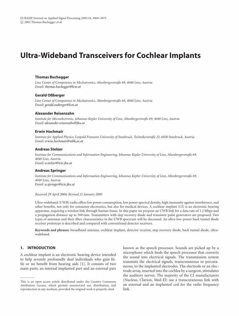
Figure 1: FCC ultra-wideband outdoor emission limits, band-width: 3.1 GHz–10.6 GHz, −41.25 dBm/MHz EIRP (equivalentisotropic radiated power).
The drawbacks of the presently used coil, for inductivetransmitting to the receiver (stimulator), are the high powerconsumption, the size, and optical reasons. On the otherside the RF link is also used for power supply and no im-planted battery is necessary. The big challenge is to substi-tute the inductive communication system with an alternativesystem like an infrared or a microwave link. A wireless ultra-wideband (UWB) system is a new low power technology forreusing previously allocated RF bands without any licensesand by hiding the signals below the noise floor [2].
UWB signals are signals where the fractional bandwidthη is greater than 0.2 or the signal occupies 0.5 GHz or moreof the spectrum [3]. The fractional bandwidth is defined as
η = 2fH − fLfH + fL
, (1)
where fH and fL are the frequencies measured at the −10 dBemissions points. Operating over a large bandwidth, UWBor impulse radio can be classified as a spread spectrum tech-nique for transmitting information. For high data rate ap-plications (up to 500 Mbps) a DS-CDMA (direct-sequencecode-division multiple access) and a multiband OFDM (or-thogonal frequency-division multiplexing) system have beenproposed to the IEEE 802.15.3a group for standardization[4]. On the other hand there is impulse radio (IR) whichis carrierless and relies on a specific unchanging pulse-typewaveforms to be transmitted in time with pulse-positionmodulation or on-off keying (OOK). IR transmitters and re-ceivers are very elementary and of low power compared toDS-CDMA and OFDM. These single-period monopulses arevery short in time duration and have a very low power spec-tral density across an ultrabroad frequency spectrum. TheUWB transmitter and its antenna can be included into thespeech processors case, the receiver and its antenna are be-neath the skin and connected to the implant. The drawback
using an UWB link, the lifetime of the implant’s battery, isof capital importance, because for every changing, a surgeryis necessary. The optimization of the implants power con-sumption demands highest priority.
2. SPECIFICATIONS
Nearly all parts of the transmitter and the receiver have tobe implemented in a submicron CMOS process to mini-mize power and size. The power consumption for the receivershould be below 100 µW as a mean value over time. The spec-trum of the UWB signal has to fulfill the FCC requirements,shown in Figure 1, in order to allow coexistence with othersystems [3, 5]. The required transmission distances are 5 to50 mm transcutaneous and 500 mm via air.
There should be a transcutaneous wireless connectionbetween speech processor and implant and on the other handoptional features, like connections to a digital music player, amobile phone, or another electronic audio device. It can alsobe envisaged to make stereo hearing possible by connectingthe ipsilateral and the contralateral implants via the speechprocessor by an UWB wireless link, through or around thehead. The antennas should be as small as possible and the ra-diated pulse should be able to penetrate human tissue withlow attenuation. The safety issues for the patient concerningelectromagnetic fields (EMF) are far below the restrictionscompared with the EMF restrictions of the WHO (WorldHealth Organization). In the United States for time-varyingelectric and magnetic fields from 0.3 to 6 GHz, a whole-bodyaverage specific absorption rate (SAR) of 0.08 W/kg and aspatial peak SAR in the head of 1.6 W/kg is permitted. If allthe maximum output of an UWB device of 0.56 mW is ab-sorbed by 1 kg of human tissue around the ear, it is still 2800times below the critical spatial peak value. If we consider thefree space loss of the link, then the absorbed power is againreduced by more than two decades. The input signal of ourtransmitter prototype is Σ∆-modulated with 1.2 Mbps, as itis also used by some CI manufacturers.
3. TRANSMITTER
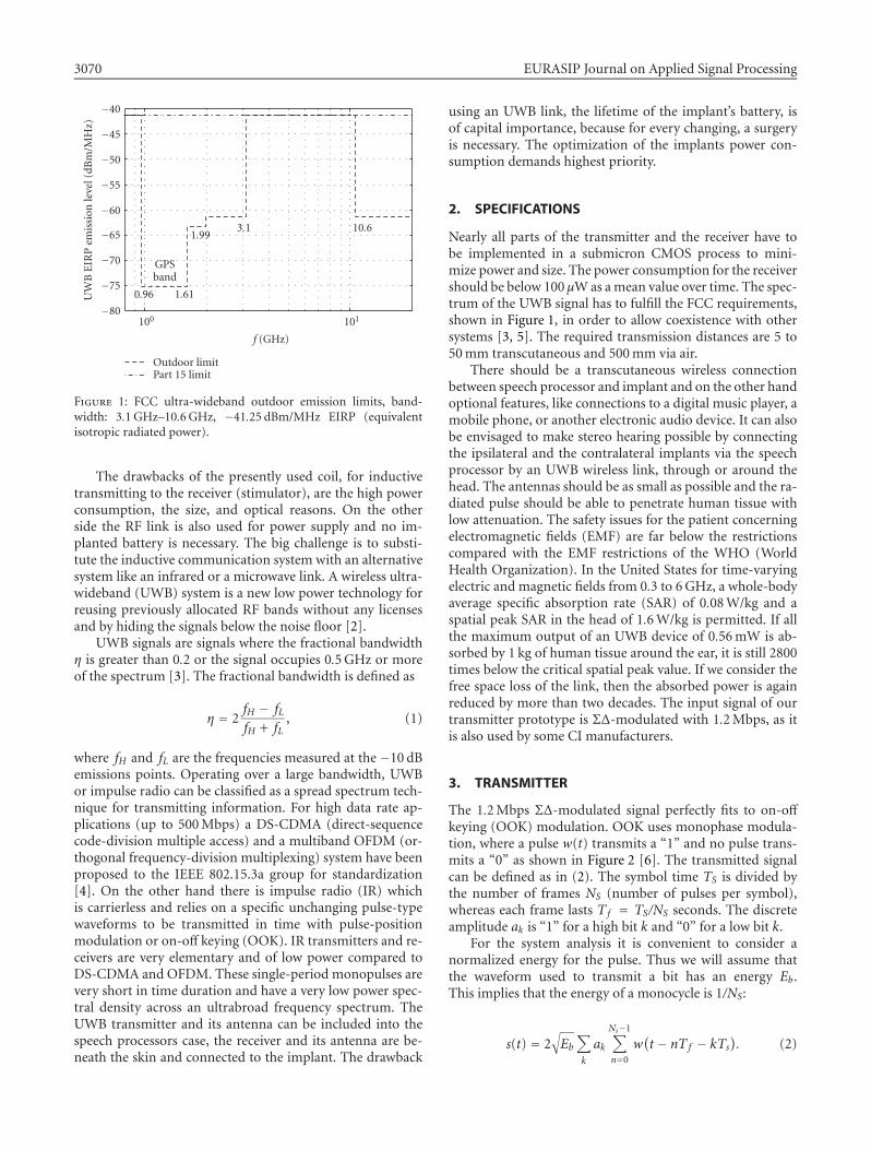
The 1.2 Mbps Σ∆-modulated signal perfectly fits to on-offkeying (OOK) modulation. OOK uses monophase modula-tion, where a pulse w(t) transmits a “1” and no pulse trans-mits a “0” as shown in Figure 2 [6]. The transmitted signalcan be defined as in (2). The symbol time TS is divided bythe number of frames NS (number of pulses per symbol),whereas each frame lasts Tf = TS/NS seconds. The discreteamplitude ak is “1” for a high bit k and “0” for a low bit k.
For the system analysis it is convenient to consider anormalized energy for the pulse. Thus we will assume thatthe waveform used to transmit a bit has an energy Eb.This implies that the energy of a monocycle is 1/NS:
s(t) = 2√Eb∑
k
ak
Ns−1∑
n=0
w(t − nTf − kTs
). (2)
Ultra-Wideband Transceivers for Cochlear Implants 3071
s(t)
Tf
1 0 1
t
Figure 2: On-off keying principle.
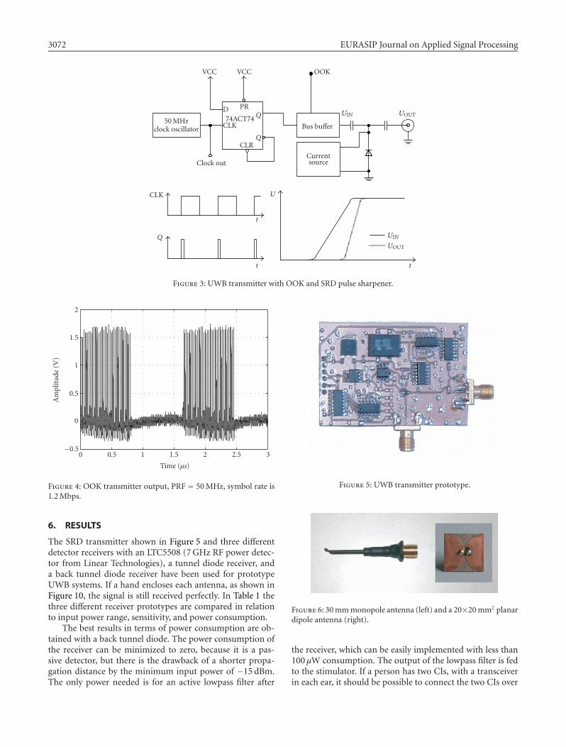
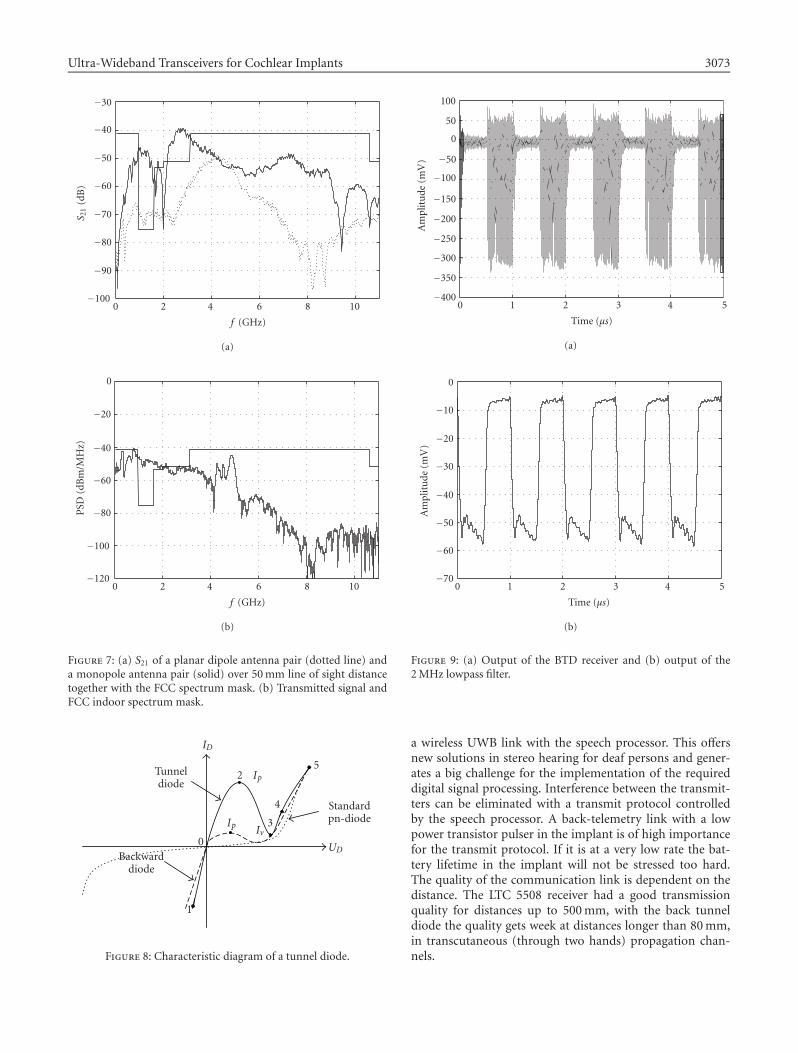
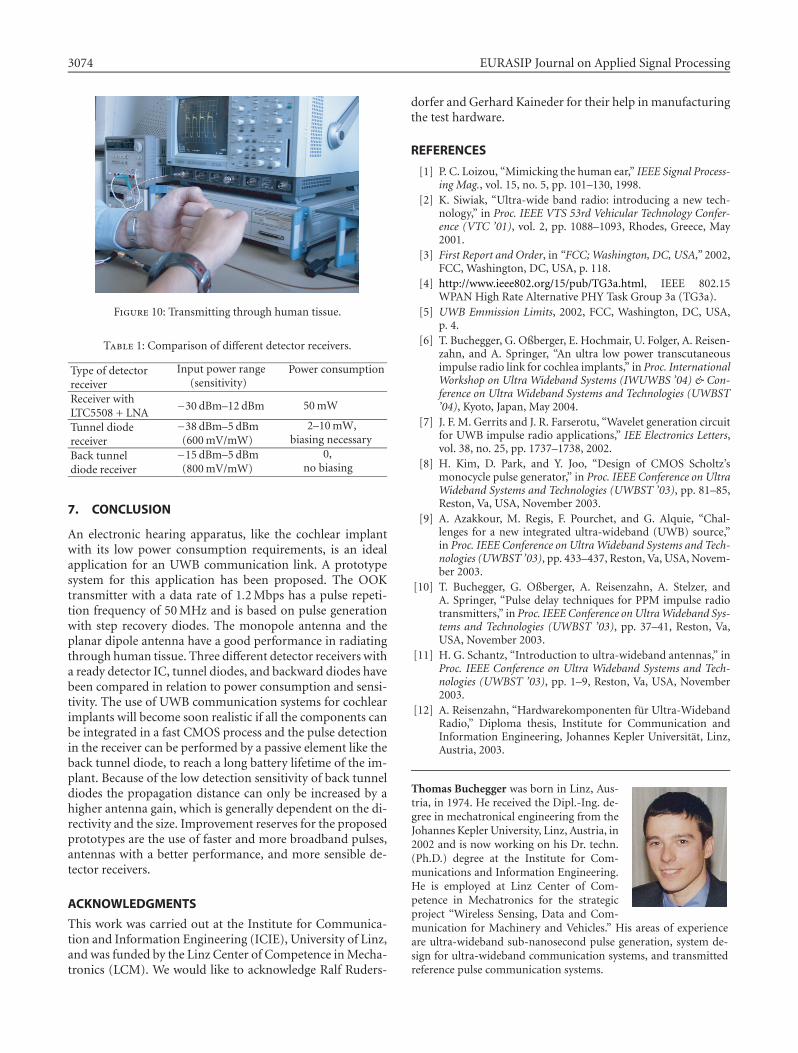
One major problem in an UWB transmitter is the pulse gen-eration with a pulse spectrum containing relevant poweronly above 3.1 GHz. The pulse duration for Gaussian mono-cycle pulses has to be below 300 ps for the spectral require-ments; therefore CMOS or SiGe BiCMOS processes are re-quired for fast pulse generation. Gerrits [7], Kim [8], andAzakkour [9] presented fundamentals to generate differ-ent pulse shapes on integrated circuits. However, CMOSis still too slow for 250 ps pulses with an amplitude of0.5 Vpp, but this goal will be reachable soon, due to rapidadvances in semiconductor technology making an ultra-low-power UWB transmitter feasible. For our prototype weused an ACT-TTL logic and a step recovery diode (SRD)pulse sharpener circuit. In Figure 3 the transmitter princi-ple is shown [10]. The 50 MHz pulse repetition frequency(PRF) is ∼ 42 times the symbol rate of 1.2 Mbps. This al-lows to transmit several pulses per bit which guarantees ahigher interference resistance and a lower power spectraldensity. The transmitter output signal is shown in Figure 4.The problem with this prototype (see Figure 5) is the highbias current of the SRD; hence for a low power applica-tion a transmitter in CMOS technology is obligatory. Byusing fast SiGe bipolar transistors (BFP 640F, etc.) insteadof the SRD, the average transmitter power can be droppedbelow 1 mW and the pulses become two times faster thanwith a SRD pulser. Further research work is planned in thisfield.
4. ANTENNA
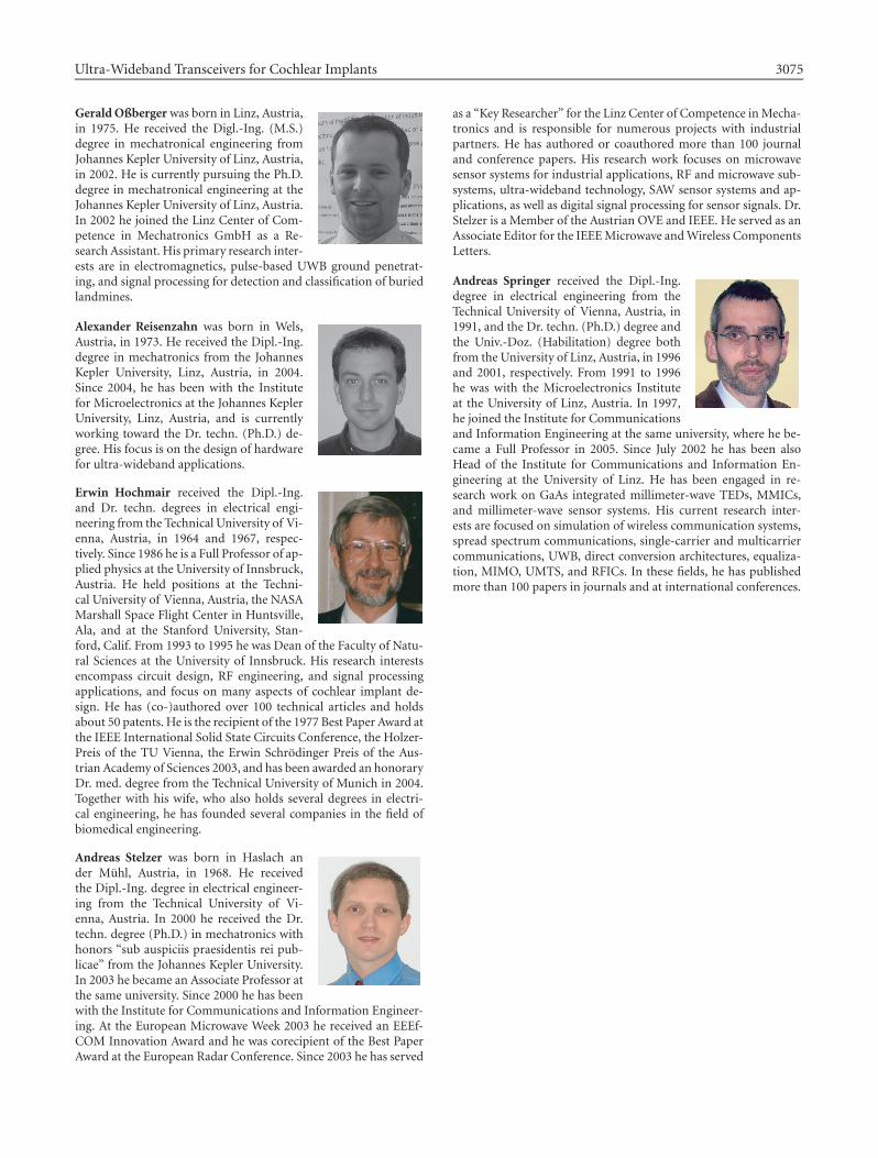
Ultra-wideband antennas are nowadays of huge interestbased on the enormous demand in broadband wireless sys-tems. Because of the small power levels authorized by theFCC, every tenth of a dB counts in an UWB system [11]. Forour prototype we used very simple monopole antennas andplanar dipole antennas shown in Figure 6 and described in[6].
The antenna, a λ/2 monopole or Marconi antenna, wasdesigned for a center frequency of 5 GHz. The groundplane is the outer conductor of the SMA connector. TheVSWR (voltage standing wave ratio) of the manually en-folded monopole antenna exhibits in the range of 1.8 GHZto 3.7 GHz a wanted poor matching, which results in nearlyno radiation below 3.7 GHz; therefore no filter to fulfill theFCC requirements is needed. The planar dipole antenna hasa much better filter performance at an attenuation differenceof 20 dB between 2 and 4 GHz as shown in Figure 7a. For our
prototype the monopole antenna was used, because the out-put pulses of the transmitter are not short enough to send thewhole power above 3 GHz. The spectrum of the transmit-ted signal produced by the transistor pulser and shaped bythe dipole antenna is shown in Figure 7b. Presently the spec-trum of the transmitted signal is not FCC compliant. A betterfit into the FCC spectrum will be reached by using a bipolartransistor pulse generator. This future pulse signal will re-sult in a higher attenuation through the human tissue, buta FDTD (finite difference time domain) antenna simulationcan improve the matching, the gain, and the filter character-istics and will compensate this problem.
5. RECEIVER
An asynchronous or noncoherent receiver is sufficient for acommunication link from the speech processor to the im-plant. The first proposed receiver prototype [6] consisted of alow noise amplifier (LNA), a detector diode, or a detector IC,which rectifies the signal and a lowpass filter for recoveringthe envelope and an operational amplifier which amplifiesthe signal back to a TTL level [12]. This type of receiver is notapplicable for implantation into the head, because of its highpower consumption in the 10–100 mW range. For less powerconsumption tunnel diodes or back tunnel diodes can beused. In the tunnel diode, the semiconductor materials usedfor forming a junction are doped to the extent of one thou-sand impurity atoms per ten million semiconductor atoms.This heavy doping produces an extremely narrow depletionzone similar to that in a Zener diode. Also because of theheavy doping, a tunnel diode exhibits an unusual current-voltage characteristic curve as compared with that of an or-dinary junction diode. The characteristic of a tunnel diodeis illustrated in Figure 8. The three most important aspectsof this characteristic are the forward current increases to apeak (IP) with a small applied forward bias, the decreasingforward current with an increasing forward bias to a min-imum valley current (IV ), and the increasing forward cur-rent with a further increase in the bias voltage. The part ofthe characteristic curve between IP and IV is the region ofnegative resistance. Backward diodes or back tunnel diodes(BTD) are tunnel diodes with a maximum forward voltageof ∼100 mV and a minimum reverse voltage of ∼400 mV.These diodes operate in reverse mode as a very sensitive pulsedetector (∼1000 mV/mW). Because of the high sensitivity nomore LNA is needed. The drawbacks of diode biasing andLNA power consumption disappear when using this diode.By using back tunnel diodes it should be possible to fulfillthe <100 µW power consumption requirement for the re-ceiver.
The backward diode is connected in reverse direction andrectifies very small signals down to−15 dBm without any bi-asing as a real passive part. The prototyped receiver only con-sists of a BTD and a resistor connected to a 2 MHz lowpassfilter. The rectified output signal of the receiver is plotted inFigure 9a. The envelope of this signal recovers the 1.2 Mhzinput signal as shown in Figure 9b.
3072 EURASIP Journal on Applied Signal Processing
Q
CLK
t
t
U
t
UOUT
UIN
Clock out
50 MHzclock oscillator
Q
Q
CLR
D PR
CLK74ACT74
Currentsource
Bus buffer
UIN UOUT
VCC VCC OOK
Figure 3: UWB transmitter with OOK and SRD pulse sharpener.
0 0.5 1 1.5 2 2.5 3
Time (µs)
−0.5
0
0.5
1
1.5
2
Am
plit
ude
(V)
Figure 4: OOK transmitter output, PRF = 50 MHz, symbol rate is1.2 Mbps.
6. RESULTS
The SRD transmitter shown in Figure 5 and three differentdetector receivers with an LTC5508 (7 GHz RF power detec-tor from Linear Technologies), a tunnel diode receiver, anda back tunnel diode receiver have been used for prototypeUWB systems. If a hand encloses each antenna, as shown inFigure 10, the signal is still received perfectly. In Table 1 thethree different receiver prototypes are compared in relationto input power range, sensitivity, and power consumption.
The best results in terms of power consumption are ob-tained with a back tunnel diode. The power consumption ofthe receiver can be minimized to zero, because it is a pas-sive detector, but there is the drawback of a shorter propa-gation distance by the minimum input power of −15 dBm.The only power needed is for an active lowpass filter after
Figure 5: UWB transmitter prototype.
Figure 6: 30 mm monopole antenna (left) and a 20×20 mm2 planardipole antenna (right).
the receiver, which can be easily implemented with less than100 µW consumption. The output of the lowpass filter is fedto the stimulator. If a person has two CIs, with a transceiverin each ear, it should be possible to connect the two CIs over
Ultra-Wideband Transceivers for Cochlear Implants 3073
0 2 4 6 8 10
f (GHz)
−100
−90
−80
−70
−60
−50
−40
−30
S 21
(dB
)
(a)
0 2 4 6 8 10
f (GHz)
−120
−100
−80
−60
−40
−20
0
PSD
(dB
m/M
Hz)
(b)
Figure 7: (a) S21 of a planar dipole antenna pair (dotted line) anda monopole antenna pair (solid) over 50 mm line of sight distancetogether with the FCC spectrum mask. (b) Transmitted signal andFCC indoor spectrum mask.
1
Backwarddiode
0
Ip Iv3
4 Standardpn-diode
5
UD
Ip2Tunneldiode
ID
Figure 8: Characteristic diagram of a tunnel diode.
0 1 2 3 4 5
Time (µs)
−400
−350
−300
−250
−200
−150
−100
−50
0
50
100
Am
plit
ude
(mV
)
(a)
0 1 2 3 4 5
Time (µs)
−70
−60
−50
−40
−30
−20
−10
0
Am
plit
ude
(mV
)
(b)
Figure 9: (a) Output of the BTD receiver and (b) output of the2 MHz lowpass filter.
a wireless UWB link with the speech processor. This offersnew solutions in stereo hearing for deaf persons and gener-ates a big challenge for the implementation of the requireddigital signal processing. Interference between the transmit-ters can be eliminated with a transmit protocol controlledby the speech processor. A back-telemetry link with a lowpower transistor pulser in the implant is of high importancefor the transmit protocol. If it is at a very low rate the bat-tery lifetime in the implant will not be stressed too hard.The quality of the communication link is dependent on thedistance. The LTC 5508 receiver had a good transmissionquality for distances up to 500 mm, with the back tunneldiode the quality gets week at distances longer than 80 mm,in transcutaneous (through two hands) propagation chan-nels.
3074 EURASIP Journal on Applied Signal Processing
Figure 10: Transmitting through human tissue.
Table 1: Comparison of different detector receivers.
Type of detectorreceiver
Input power range(sensitivity)
Power consumption
Receiver withLTC5508 + LNA
−30 dBm–12 dBm 50 mW
Tunnel diodereceiver
−38 dBm–5 dBm(600 mV/mW)
2–10 mW,biasing necessary
Back tunneldiode receiver
−15 dBm–5 dBm(800 mV/mW)
0,no biasing
7. CONCLUSION
An electronic hearing apparatus, like the cochlear implantwith its low power consumption requirements, is an idealapplication for an UWB communication link. A prototypesystem for this application has been proposed. The OOKtransmitter with a data rate of 1.2 Mbps has a pulse repeti-tion frequency of 50 MHz and is based on pulse generationwith step recovery diodes. The monopole antenna and theplanar dipole antenna have a good performance in radiatingthrough human tissue. Three different detector receivers witha ready detector IC, tunnel diodes, and backward diodes havebeen compared in relation to power consumption and sensi-tivity. The use of UWB communication systems for cochlearimplants will become soon realistic if all the components canbe integrated in a fast CMOS process and the pulse detectionin the receiver can be performed by a passive element like theback tunnel diode, to reach a long battery lifetime of the im-plant. Because of the low detection sensitivity of back tunneldiodes the propagation distance can only be increased by ahigher antenna gain, which is generally dependent on the di-rectivity and the size. Improvement reserves for the proposedprototypes are the use of faster and more broadband pulses,antennas with a better performance, and more sensible de-tector receivers.
ACKNOWLEDGMENTS
This work was carried out at the Institute for Communica-tion and Information Engineering (ICIE), University of Linz,and was funded by the Linz Center of Competence in Mecha-tronics (LCM). We would like to acknowledge Ralf Ruders-
dorfer and Gerhard Kaineder for their help in manufacturingthe test hardware.
REFERENCES
[1] P. C. Loizou, “Mimicking the human ear,” IEEE Signal Process-ing Mag., vol. 15, no. 5, pp. 101–130, 1998.
[2] K. Siwiak, “Ultra-wide band radio: introducing a new tech-nology,” in Proc. IEEE VTS 53rd Vehicular Technology Confer-ence (VTC ’01), vol. 2, pp. 1088–1093, Rhodes, Greece, May2001.
[3] First Report and Order, in “FCC; Washington, DC, USA,” 2002,FCC, Washington, DC, USA, p. 118.
[4] http://www.ieee802.org/15/pub/TG3a.html, IEEE 802.15WPAN High Rate Alternative PHY Task Group 3a (TG3a).
[5] UWB Emmission Limits, 2002, FCC, Washington, DC, USA,p. 4.
[6] T. Buchegger, G. Oßberger, E. Hochmair, U. Folger, A. Reisen-zahn, and A. Springer, “An ultra low power transcutaneousimpulse radio link for cochlea implants,” in Proc. InternationalWorkshop on Ultra Wideband Systems (IWUWBS ’04) & Con-ference on Ultra Wideband Systems and Technologies (UWBST’04), Kyoto, Japan, May 2004.
[7] J. F. M. Gerrits and J. R. Farserotu, “Wavelet generation circuitfor UWB impulse radio applications,” IEE Electronics Letters,vol. 38, no. 25, pp. 1737–1738, 2002.
[8] H. Kim, D. Park, and Y. Joo, “Design of CMOS Scholtz’smonocycle pulse generator,” in Proc. IEEE Conference on UltraWideband Systems and Technologies (UWBST ’03), pp. 81–85,Reston, Va, USA, November 2003.
[9] A. Azakkour, M. Regis, F. Pourchet, and G. Alquie, “Chal-lenges for a new integrated ultra-wideband (UWB) source,”in Proc. IEEE Conference on Ultra Wideband Systems and Tech-nologies (UWBST ’03), pp. 433–437, Reston, Va, USA, Novem-ber 2003.
[10] T. Buchegger, G. Oßberger, A. Reisenzahn, A. Stelzer, andA. Springer, “Pulse delay techniques for PPM impulse radiotransmitters,” in Proc. IEEE Conference on Ultra Wideband Sys-tems and Technologies (UWBST ’03), pp. 37–41, Reston, Va,USA, November 2003.
[11] H. G. Schantz, “Introduction to ultra-wideband antennas,” inProc. IEEE Conference on Ultra Wideband Systems and Tech-nologies (UWBST ’03), pp. 1–9, Reston, Va, USA, November2003.
[12] A. Reisenzahn, “Hardwarekomponenten fur Ultra-WidebandRadio,” Diploma thesis, Institute for Communication andInformation Engineering, Johannes Kepler Universitat, Linz,Austria, 2003.
Thomas Buchegger was born in Linz, Aus-tria, in 1974. He received the Dipl.-Ing. de-gree in mechatronical engineering from theJohannes Kepler University, Linz, Austria, in2002 and is now working on his Dr. techn.(Ph.D.) degree at the Institute for Com-munications and Information Engineering.He is employed at Linz Center of Com-petence in Mechatronics for the strategicproject “Wireless Sensing, Data and Com-munication for Machinery and Vehicles.” His areas of experienceare ultra-wideband sub-nanosecond pulse generation, system de-sign for ultra-wideband communication systems, and transmittedreference pulse communication systems.
Ultra-Wideband Transceivers for Cochlear Implants 3075
Gerald Oßberger was born in Linz, Austria,in 1975. He received the Digl.-Ing. (M.S.)degree in mechatronical engineering fromJohannes Kepler University of Linz, Austria,in 2002. He is currently pursuing the Ph.D.degree in mechatronical engineering at theJohannes Kepler University of Linz, Austria.In 2002 he joined the Linz Center of Com-petence in Mechatronics GmbH as a Re-search Assistant. His primary research inter-ests are in electromagnetics, pulse-based UWB ground penetrat-ing, and signal processing for detection and classification of buriedlandmines.
Alexander Reisenzahn was born in Wels,Austria, in 1973. He received the Dipl.-Ing.degree in mechatronics from the JohannesKepler University, Linz, Austria, in 2004.Since 2004, he has been with the Institutefor Microelectronics at the Johannes KeplerUniversity, Linz, Austria, and is currentlyworking toward the Dr. techn. (Ph.D.) de-gree. His focus is on the design of hardwarefor ultra-wideband applications.
Erwin Hochmair received the Dipl.-Ing.and Dr. techn. degrees in electrical engi-neering from the Technical University of Vi-enna, Austria, in 1964 and 1967, respec-tively. Since 1986 he is a Full Professor of ap-plied physics at the University of Innsbruck,Austria. He held positions at the Techni-cal University of Vienna, Austria, the NASAMarshall Space Flight Center in Huntsville,Ala, and at the Stanford University, Stan-ford, Calif. From 1993 to 1995 he was Dean of the Faculty of Natu-ral Sciences at the University of Innsbruck. His research interestsencompass circuit design, RF engineering, and signal processingapplications, and focus on many aspects of cochlear implant de-sign. He has (co-)authored over 100 technical articles and holdsabout 50 patents. He is the recipient of the 1977 Best Paper Award atthe IEEE International Solid State Circuits Conference, the Holzer-Preis of the TU Vienna, the Erwin Schrodinger Preis of the Aus-trian Academy of Sciences 2003, and has been awarded an honoraryDr. med. degree from the Technical University of Munich in 2004.Together with his wife, who also holds several degrees in electri-cal engineering, he has founded several companies in the field ofbiomedical engineering.
Andreas Stelzer was born in Haslach ander Muhl, Austria, in 1968. He receivedthe Dipl.-Ing. degree in electrical engineer-ing from the Technical University of Vi-enna, Austria. In 2000 he received the Dr.techn. degree (Ph.D.) in mechatronics withhonors “sub auspiciis praesidentis rei pub-licae” from the Johannes Kepler University.In 2003 he became an Associate Professor atthe same university. Since 2000 he has beenwith the Institute for Communications and Information Engineer-ing. At the European Microwave Week 2003 he received an EEEf-COM Innovation Award and he was corecipient of the Best PaperAward at the European Radar Conference. Since 2003 he has served
as a “Key Researcher” for the Linz Center of Competence in Mecha-tronics and is responsible for numerous projects with industrialpartners. He has authored or coauthored more than 100 journaland conference papers. His research work focuses on microwavesensor systems for industrial applications, RF and microwave sub-systems, ultra-wideband technology, SAW sensor systems and ap-plications, as well as digital signal processing for sensor signals. Dr.Stelzer is a Member of the Austrian OVE and IEEE. He served as anAssociate Editor for the IEEE Microwave and Wireless ComponentsLetters.
Andreas Springer received the Dipl.-Ing.degree in electrical engineering from theTechnical University of Vienna, Austria, in1991, and the Dr. techn. (Ph.D.) degree andthe Univ.-Doz. (Habilitation) degree bothfrom the University of Linz, Austria, in 1996and 2001, respectively. From 1991 to 1996he was with the Microelectronics Instituteat the University of Linz, Austria. In 1997,he joined the Institute for Communicationsand Information Engineering at the same university, where he be-came a Full Professor in 2005. Since July 2002 he has been alsoHead of the Institute for Communications and Information En-gineering at the University of Linz. He has been engaged in re-search work on GaAs integrated millimeter-wave TEDs, MMICs,and millimeter-wave sensor systems. His current research inter-ests are focused on simulation of wireless communication systems,spread spectrum communications, single-carrier and multicarriercommunications, UWB, direct conversion architectures, equaliza-tion, MIMO, UMTS, and RFICs. In these fields, he has publishedmore than 100 papers in journals and at international conferences.
Related Documents