Ultra-low-power Digitally-controlled Oscillator for Event-driven Transmitter By Ao Ba Delft University of Technology, July 2011 A thesis submitted to the Electrical Engineering, Mathematics and Computer Science Department of Delft University of Technology in partial fulfillment of the requirements for the degree of Master of Science. Delft University of Technology, the Netherlands © Copyright by Ao Ba, July 2011

Welcome message from author
This document is posted to help you gain knowledge. Please leave a comment to let me know what you think about it! Share it to your friends and learn new things together.
Transcript

Ultra-low-power Digitally-controlled Oscillator
for Event-driven Transmitter
By
Ao Ba
Delft University of Technology, July 2011
A thesis submitted to the Electrical Engineering, Mathematics and Computer
Science Department of Delft University of Technology in partial fulfillment of
the requirements for the degree of Master of Science.
Delft University of Technology, the Netherlands
© Copyright by Ao Ba, July 2011

2
Approval
Name: Ao Ba
Degree: Master of Science
Title of Thesis: Ultra-low-power Digitally-controlled Oscillator
for Event-driven Transmitter
Committee in Charge of Approval:
Chair:
Professor John R. Long
Department of Microelectronics
Committee Members:
Professor Marco Spirito
Department of Microelectronics
Professor Michiel A.P. Pertijs
Department of Microelectronics
Ir. Xiongchuan Huang
Holst centre/imec the Netherlands

3
Contents
Chapter 1 Introduction ........................................................................................................ 5
1.1 Event-driven wireless communication ....................................................................... 5
1.1.1 Wireless communication ................................................................................ 5
1.1.2 Event-driven and data-driven communication ................................................ 7
1.2 Ultra-low-power transmitter ..........................................................................9
1.3 Digitally-controlled oscillator........................................................................ 11
1.4 Outline of this thesis .................................................................................... 13
Chapter 2 Transmitter specification and architecture ............................ 15
2.1 Transmitter specification ............................................................................................15
2.1.1 Design background ....................................................................................... 15
2.1.2 Design specification ..................................................................................... 17
2.2 State-of-the-art designs ............................................................................... 22
2.3 Proposed architecture .................................................................................. 26
2.3.1 Potential solutions ....................................................................................... 26
2.3.2 Power consumption investigation ................................................................. 28
2.3.1 Conclusions .................................................................................................. 30
2.4 Conclusions ....................................................................................................................31
Chapter 3 Oscillator design .................................................................... 34
3.1 General considerations ...............................................................................................34
3.1.1 Power consumption ..................................................................................... 34
3.1.2 Frequency tuning ......................................................................................... 36
3.1.3 Phase noise .................................................................................................. 37
3.1.4 Conclusions .................................................................................................. 38
3.2 Active part ......................................................................................................................39
3.2.1 Circuit topology ............................................................................................ 39
3.2.2 Transistor sizing............................................................................................ 41
3.2.3 Biasing ......................................................................................................... 42
3.2.4 Conclusions .................................................................................................. 43
3.3 Varactor banks ..............................................................................................................43
3.3.1 LSB cell......................................................................................................... 44
3.3.2 Varactor matrix ............................................................................................ 46
3.3.3 Bias decoupling ............................................................................................ 47
3.4 Physical layout ............................................................................................. 48
3.5 Simulation results ........................................................................................ 49
3.5.1 Parasitic modeling ........................................................................................ 49
3.5.2 Frequency tuning ......................................................................................... 52
3.5.3 Phase noise and power consumption ........................................................... 53
3.6 Conclusions ....................................................................................................................55

4
Chapter 4 Measurement results ................................................................................... 57
4.1 Chip gallery .................................................................................................. 57
4.2 Measurement set-up.................................................................................... 58
4.3 Measurement results ................................................................................... 59
4.3.1 Frequency tuning ......................................................................................... 59
4.3.2 Power consumption and phase noise ........................................................... 63
4.4 Conclusions and comparisons ...................................................................................66
Chapter 5 Conclusions ........................................................................................................69

5
Chapter 1
Introduction
Wireless communication is a key technology in modern civilization. After more than a
century’s phenomenal development, it has become a practical application from a
scientists’ dream. Although the wireless industry is mature in many aspects
nowadays, the advancement of semiconductor and integrated circuit technologies
promotes many new research motives. Event-driven wireless communication is a
promising concept that presents new challenges to designers. For an event-driven
transmitter, achieving high efficiency under the condition of ultra-low-power (ULP)
consumption is one of the most critical tasks. It places emphasis on the importance
of carrier generation. This is the motivation of this thesis, which mainly focuses on
designing a ULP digitally-controlled oscillator (DCO) for event-driven transmitters.
In this chapter, wireless communication technology will be briefly overviewed, and
then the concept of event-driven communication is introduced. Afterwards, the
importance of RF oscillator design will be explained. Meanwhile, the operating
principle of a digitally-controlled oscillator and its advantages will be presented.
Finally, the contents of this thesis are outlined.
1.1 Event-driven wireless communication
This section firstly gives a short overview of the wireless communication industry,
and then different wireless communication technologies are discussed and classified
into two types. Finally, the concepts of data-driven and event-driven are introduced.
1.1.1 Wireless communication
The 21st century is expected to be the Information Age. The information and
communication technology (ICT) revolution started in last century is ongoing, but has
already changed the world deeply. Its profound effects on socioeconomic and
cultural factors make it comparable to the Industrial Revolution. There are two key
improvements in the ICT revolution: the ability to process information and the
convenience of exchanging information. The second part drives the fast development
of communication technology. Instant global communication helps consumers find
the provider who can offer the lowest price. People at home can share the happiness
with the live spectators of a football game through the power of digital TV
broadcasting. The development of communication technology is one of the most
6
important drives of the ICT revolution.
Fig.1-1 Number of Wireless subscribers boomed in recently years [3]
Wireless communication is a key element of modern telecommunication. The
revenue from wireless data and service in the USA is valued at 194.1 billion dollars in
2009 [1]. The number of worldwide mobile subscribers reached 5 billion dollars in
2010 [1]. In the Netherlands, mobile phone use per person was 1.2 in 2009 [2]. Even
in developing countries such as China and India, this number reached 0.6 in 2011 [2].
On the other hand, the number of landline subscribers worldwide kept falling, as
more and more users rely on wireless communication to keep in touch with the
outside world.
Without the use of wires, wireless communication takes the advantage of the
electromagnetic (EM) waves. As the propagation of EM waves does not need any
medium and the speed is almost instant, wireless communication offers the highest
level of convenience to transfer information. The history of wireless communication
dates back to the 19th century. In 1861, the Scottish physicist and mathematician
James Clerk Maxwell predicted the existence of EM waves, which was demonstrated
by Hertz in 1886. In the late 19th century, inventors such as Nikola Tesla worked to
demonstrate the possibility of wireless communication by transmitting and receiving
electromagnetic waves. But Guglielmo Marconi transmitted a wireless signals (the
Morse telegraph “s” - three dots) across the Atlantic Ocean for the first time in 1901

7
[4]. With the subsequent invention of vacuum tubes and transistors, wireless
communication became available to the public in applications such as wireless
telegraphy, AM and FM radio.
After a century’s fast development, no matter from the perspective of technique or
business, wireless communication is in many aspects a mature market now. The use
of EM spectrum is strictly regulated by governments. Various organizations or
alliances compete with each other to develop advanced wireless communication
standards. Substantial wireless applications have covered almost all aspects of
people’s lives. GSM/CDMA cellular networks are updated to 3G mobile standards for
higher data rate. More and more handheld devices support Wi-Fi to access wireless
hotspots in airports, offices or even coffee shops. Wireless personal area network
(WPAN) is being enabled by the promotion of Bluetooth and Zigbee. Other new
wireless applications such as wireless sensor network (WSN) and wireless body area
network (WBAN) are currently under development, but there are numerous relevant
papers published every year.
Fig.1-2 Left: U.S. shipboard transmitter in World War 1 [5] Right: Tiny Wi-Fi chip [6]
1.1.2 Event-driven and data-driven communication
All of these different wireless communication applications can be classified into two
types: data-driven and event-driven. The data-driven type aims for delivering large
amount of information. Wi-Fi is a typical data-driven application. Data rate is
therefore the most important benchmark. Faster data exchange is the target for the
next generation technology. The IEEE 802.11b standard released in 1999 was not the
earliest one but was rapidly accepted as the definitive wireless local area network
(WLAN) technology. The maximum throughput was only 11Mbit/s initially. In 2009,
the latest standard (IEEE 802.11n) was published and could support a data-rate up to

8
600Mbit/s. The continuing increase in data rate keeps Wi-Fi at the top of WLAN
standards.
The event-driven type of communication, on the other hand, is designed for a
different purpose. It aims to share information of unexpected events instantly. The
amount of information exchanged each time is not huge, but the information may be
important and needs to be delivered on time. Also, the communication events are
sporadic and unpredictable. Data rate is not the bottleneck for event-driven
communication, but efficiency is important. The system must fulfill its duty at the
lowest power, cost and minimum time. The application areas of event-driven
communication include industrial, environmental and healthcare monitoring, where
wireless devices need to maintain responsiveness to irregular events, especially
emergency or hazardous incidents.
Fig.1-3 Classification of wireless communications and application examples [7].
Fig.1-3 illustrates the characteristic and examples of data-driven and event-driven
wireless communication. Although practical applications always require both of these
two communication types, the different emphasis present different challenges to the
system designer. Certain applications should be optimized specifically for a particular
purpose. The system requirements for data-driven applications are:
1. High data rate (>1Mbps);
2. Complex modulation and/or large instantaneous bandwidth;
3. High selectivity for multi-channel coexistence;
4. High efficiency in frequency spectrum usage;
5. Fast start-up time for duty-cycled operation.
Event-driven communication requires the system to be optimized for:
1. Low data rate (<1Mbps);
2. Ultra-low power consumption for long battery lifetime (<1mW);
3. Low communication latency for in-time delivery of urgent information;
4. Relaxed spectrum efficiency and selectivity due to the scarce network traffic.

9
1.2 Ultra-low-power transmitter
No matter data-driven or event-driven wireless communications, the wireless system
consists of a transmitter and a receiver. The transmitter is responsible to transmit EM
waves piggybacking useful information and the receiver’s duty is to process the
wireless signal and recover the information. Normally, data cannot is modulated on a
carrier signal. The first reason is due to the antenna. To achieve a reasonable
efficiency, the size of the antenna should be at least one-tenth the wavelength of the
carrier. Considering the speed of light and the simple formula fc , transmitting a
20-20k Hz acoustical signal directly, the size of the antenna is on the order of
kilometers and is thus impractical for any system. The second reason is multiplexing.
If several similar signals are transmitted simultaneously, they will disturb each other
and cannot be distinguished by the receiver. Modulating the original information
onto different carriers enables multiple wireless devices operating without
interference in a common physical space.
Fig.1-4 A block diagram of common wireless transmitter
In general, the architecture of a wireless transmitter is shown in Fig.1-4. The carrier
generation, which is normally an oscillator, provides a pure, high-frequency,
sinusoidal waveform. The useful data is loaded onto the carrier by modulating the
amplitude, frequency or phase of the carrier signal. The modulated signal is then
amplified to expected energy level by the power amplifier. Alternating voltage and
current are finally converted to electromagnetic waves and radiated into free space
by the antenna.

10
Event-driven communication includes lots of new applications in today’s wireless
market such as Zigbee and active RFID. Behind the promising prospects are new
challenges for transmitter design. Although the requirement for data rate is relaxed
and the architecture is not necessarily complex to support additional functionalities,
maintaining high efficiency under the condition of ultra-low-power consumption is
still difficult. The power efficiency of the transmitter can be calculated as
PApre
outTx
PP
P
. (1-1)
outP is the power radiated into free space, PAP
is the power consumed by the
power amplifier from power supply, and preP
is the power consumed by all of the
transmitter blocks before the power amplifier. Meanwhile, the drain efficiency of the
power amplifier can be calculated as
PA
out
PAP
P
. (1-2)
Eqn.1-1 can be rewritten in another way to show more insight for the ULP
transmitter design:
PAout
preTx
P
P
1
1
. (1-3)
For some high-speed, high-power applications such as the cellular phone system,
outP can be as high as 30dBm, which is much larger than preP . Therefore the
efficiency of the total transmitter Tx is dominated by PA . However, for ULP
transmitters outP is normally below 0dBm, which is comparable to preP . preP will
reduce the overall efficiency significantly. For example, if both preP and outP are
1mW and PA is 50%, the efficiency of the total transmitter Tx is just 25%. It can
be concluded that for ULP transmitter design, optimizing the pre-PA stage to
minimize its power consumption is very crucial to achieve high power efficiency.

11
1.3 Digitally-controlled oscillator
The RF carrier generation block of Fig.1-4 is a critical part of the pre-PA stage.
Modern communication systems normally use different kinds of oscillators to
generate carrier signals. LC oscillators with a fixed inductor and variable capacitor are
popular, thanks to their good performance and easy design approach. An LC oscillator
can be divided into two parts, the LC resonator and the active device. Oscillation
occurs when electrical and magnetic energy in the tank exchange between the
capacitor and the inductor. The oscillation frequency is determined ideally by
LCf
2
1 . (1-4)
The LC resonator tank dissipates energy and the loss of the tank is modeled as a
parallel resistor. To maintain a stable oscillation, the active part of the oscillator is
designed to overcome the loss in the tank. Despite of a lot of possible ways to
implement the active part, the basic principle of the LC oscillator is the same.
The value of the inductor is normally fixed. Frequency tuning is achieved by changing
the value of the capacitor (varactor). However, this is quite a challenging task for a
low-voltage deep-submicrometer CMOS oscillator, due to its highly nonlinear
frequency-voltage characteristics and low-voltage headroom, which are shown in
Fig.1-5 [8].
Fig.1-5 Idealized capacitance versus voltage curves of a MOS varactor for both a
traditional and a deep-submicrometer CMOS process [8]
12
The useful range of the tuning curve in a deep-submicrometer process is very limited
and the curve is sharp in this range. Any noise or voltage vibrations will easily
degrade the stability of the oscillator, and the control voltage must be very precise to
choose a certain frequency. To overcome these disadvantages, a new approach
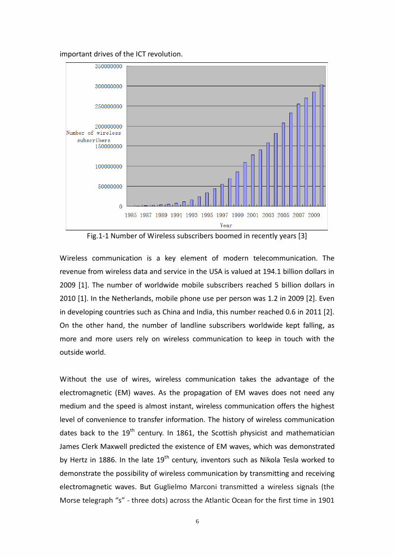
introduced in [8] makes use of the two flat ranges in the tuning curve of a varactor.
Compared to normal voltage-controlled oscillators (VCOs), the control signal of the
digitally-controlled oscillator (DCO) is not an analogue control voltage, but digital bits.
Each bit controls a small varactor, biasing the varactor either in an on-state or
off-state. The architecture can be illustrated in Fig.1-6. The more varactor cells are
turned on, the higher the oscillation frequency will be. The frequency can be
calculated from [8]
1
0
*2
1
N
k
kCL
f
. (1-5)
The inductor is still fixed, but the value of the capacitor is a sum of all the small
varactor cells. As the value of the total varactor bank changes step by step, the
changing of the frequency is also discrete, and the resolution is determined by the
size of each varactor cell in the bank. The advantages of the DCO are obvious. Firstly,
the varactor is biased on the flat range. As shown in Fig.1-5, the slope of the
capacitance-voltage curve on this range is close to zero, which makes the oscillator
immune to any unwanted disturbances from the control signal. Secondly, DCO is
suitable for low-voltage applications as the frequency tuning is not limited by the
supply voltage headroom. Thirdly, the frequency tuning resolution can always be
improved by new generation technologies and high-speed dithering. For
ultra-low-power applications, DCOs offer more benefits. A frequency synthesizer is
power-hungry and is often duty-cycled in ULP transceivers. Providing a constant and
stable tuning voltage for VCOs requires a DAC or a large capacitor, while DCOs only
need digital registers to lock the tuning bits. Digital registers consumes nearly no
static power and do not suffer any decay, which makes DCOs more suitable for ULP
applications where the LO is not in a continuous PLL/FLL loop. Oscillation frequency
is calibrated periodically, and most of the time the frequency tuning word is kept
constant.
Fig.1-6 Block diagram of a DCO

13
1.4 Outline of this thesis
This thesis focuses on the design of an ultra-low-power digitally-controlled oscillator
for event-driven transmitters. The next chapters are organized as follows. In Chapter
2, the specification of the ULP transmitter is introduced, and then some
state-of-the-art transmitter designs and potential solutions are summarized. Their
advantages and disadvantages are also discussed and compared. Finally, a suitable
architecture is proposed. In Chapter 3, the design process of the DCO is analyzed in
detail. The weak inversion bias technique is applied for the active part design to
reduce power consumption. The varactor bank is the most critical block. Design
problems, such as how to implement each LSB cell, how to control all these cells
efficiently and how to optimize the layout to achieve minimized loss and parasitic
effects are analyzed. Finally, Chapter 4 presents the measurement results and some
useful comments and conclusion are summarized in Chapter 5.

14
References
[1] “Telecommunications Industry overview”. Plunkett Research Ltd. Retrieved 2010,
from
http://www.plunkettresearch.com/Telecommunications%20market%20research/indu
stry%20statistics
[2] “Number of mobile phone in use”. Wikipedia. Retrieved 06-2011, from
http://en.wikipedia.org/wiki/List_of_countries_by_number_of_mobile_phones_in_u
se#cite_note-1
[3] “CTIA's Semi-Annual Wireless Industry Survey”. CTIA. Retrieved 2011, from
http://www.ctia.org/advocacy/research/index.cfm/AID/10538
[4] Robert White. “Aerial Assistance with a Kite”. The Journal of the American
Kitefliers Association, Vol. 23, Issue 5, 11-2011.
[5] “Who Invented Radio?” PBS. Retrieved 2011, from
http://www.pbs.org/tesla/ll/ll_whoradio.html
[6] “Tiny wireless memory chip debuts”. BBC News. Retrieved 07-2006, from
http://news.bbc.co.uk/2/hi/technology/5186650.stm?www.dailytech.com
[7] X. Huang. “Event-driven radio background”. IMEC-NL. Internal report. 05-2011.
[8] R.B.Staszewski, C.-M.Hung, D.Leipold, and P.T.Balsara. “A first multigigahertz
digitally controlled oscillator for wireless applications”. IEEE Transactions on
Microwave Theory and Techniques, vol. 51, no. 11, pp. 2154–2164, Nov. 2003.

15
Chapter 2
Transmitter specification and architecture
The last chapter has introduced the background knowledge for this design. This
chapter goes a step further to describe the transmitter specification and architecture.
Design requirements are first presented, and then some state-of-the-art designs are
summarized, with their advantages and disadvantages also discussed. After
proposing two potential solutions and analyzing their power consumption, the circuit
architecture of this transmitter is chosen.
2.1 Transmitter specification
The design background of this work is given. Based on the targeted application
environments, the design specification is defined. The modulation type, carrier
frequency and power consumption of the event-driven transmitter are discussed
respectively.
2.1.1 Design background
This design project belongs to the event-driven radio work package, which is part of
the wireless autonomous transducer solutions (WATS) program at IMEC-NL. This
work package aims to implement an RF transceiver module that consumes a
negligible quantity of power. With the assistance of energy scavenging technology,
the transceiver module will be able to achieve autonomous operation. The targeted
application is not strictly defined. However, the complete transceiver module should
support many different event-driven applications, which are not feasible with
traditional transceivers. Potential applications include: active RFID, smart building,
industrial control and medical monitoring. Some of them are illustrated in Fig.2-1. All
of these applications are powered by batteries, so the power consumption should be
minimized to achieve longer battery lifetime. The data rate is not necessary to be
high as the data needed to be transmitted is some control signals. However, the
wake-up time is critical, for medical applications the health information of a parent
must be updated instantly.

16
Fig.2-1 Potential applications for the event-driven radio
Currently, a ULP event-driven receiver has been designed [1]. The circuit architecture
is showed in Fig.2-2. It makes use of an envelope detector to demodulate OOK
signals. This receiver can support different ISM frequency bands, ranging from
780MHz to 950MHz. By using a double-sampling technique to suppress DC offset and
low-frequency noise, this receiver achieves considerable sensitivity and very low
power consumption. The gain of the RF front end is tunable, which enables the
receiver to achieve different sensitivity, data rate and power consumption
requirements in various applications. The measured sensitivity versus data-rate
curves in different gain modes are illustrated in Fig.2-3 [2]. The sensitivity is defined
as the minimum power of the input RF signals to achieve a bit error rate (BER) no
larger than 0.1%.
Fig.2-2 Event-driven receiver circuit block diagram [2]

17
Fig.2-3 Sensitivity versus data-rate curves in different gain modes [2]
2.1.2 Design specification
To achieve two-way communication, a transmitter should be designed to work in
coordination with the receiver. It needs to be compatible with the current receiver,
which means that it should support the identical modulation scheme and use the
same frequency bands. Also, its power consumption should be as low as possible.
However, as the transmitter and the receiver will make up a complete event-driven
transceiver to cover various application areas, optimizing the overall performance of
the transceiver requires a balanced power budget between them. The design
specification of this transmitter will be analyzed in each aspect as follows.
A. Modulation
On-off-keying (OOK) is the simplest amplitude modulation scheme. Transmitting
certain duration of the carrier signals means a binary one, and a binary zero is simply
represented by the absence of the carrier. As the information is embedded in the
amplitude of the carrier, and the amplitude is very susceptible to noise and
interference, OOK modulation is not suitable for high speed communication. But for
event-driven applications, it has many advantages. As for frequency and phase
modulation, the amplitude of the carrier is constant, either a “0” or a “1” is
transmitted, the output power is always constant. For OOK modulation, the output
power is zero when transmitting a “0”, so the power amplifier and some other circuit
blocks can simply be turned off. This roughly saves 50% power consumption of the
power amplifier. OOK modulation also relaxes the complexity of the total system. As
the receiver uses an envelope detector to demodulate OOK signals, the accuracy and

18
purity of the carrier frequency is not critical, as long as it is within the desired
frequency band. Therefore, the carrier generation of the transmitter can be mainly
optimized for power consumption while relaxing other specifications.
B. Frequency band
Table.2-1 ISM frequency bands in different regions [3]
(WMTS: wireless medical telemetry services)
(MICS: medical implant communication service)
Region Frequency band
Worldwide 2400-2500MHz
Japan 950-958MHz
US 902-928MHz
EU 863-870MHz
China 779-787MHz
EU 433.05-434.79MHz
Japan(WMTS) 420-450MHz
US/EU(MICS) 402-405MHz
Frequency spectrum is a scarce resource. Its usage is strictly controlled by
government institutions, such as the FCC in US, ETSI in Europe and ITU globally. The
industrial, scientific and medical (ISM) bands can be used license-free under some
rules. The ISM bands for different regions are summarized in Table.2-1. If working in
the 2.4GHz ISM band, the transceiver can be used worldwide without any
modification. However, the transceiver will consume more power, as RF gain at
2.4GHz is more difficult to obtain than at 900MHz or 400MHz. Also, as the free-space
path loss is proportional to the square of the carrier frequency, the high frequency
carrier suffers larger propagation loss. On the other hand, if the 400MHz ISM band is
used, the size of the antenna is much larger. It will increase the cost of the system
and makes it unsuitable for miniature applications. Sub-GHz frequency bands ranging
from 780MHz to 950MHz are more suitable for this project as a trade-off between
power consumption, cost and size. However, to cover all of the bands in different
19
regions, the transmitter must have wide frequency range, or should easily be
modified to work in different frequency bands by only changing some parameters.
C. Output power
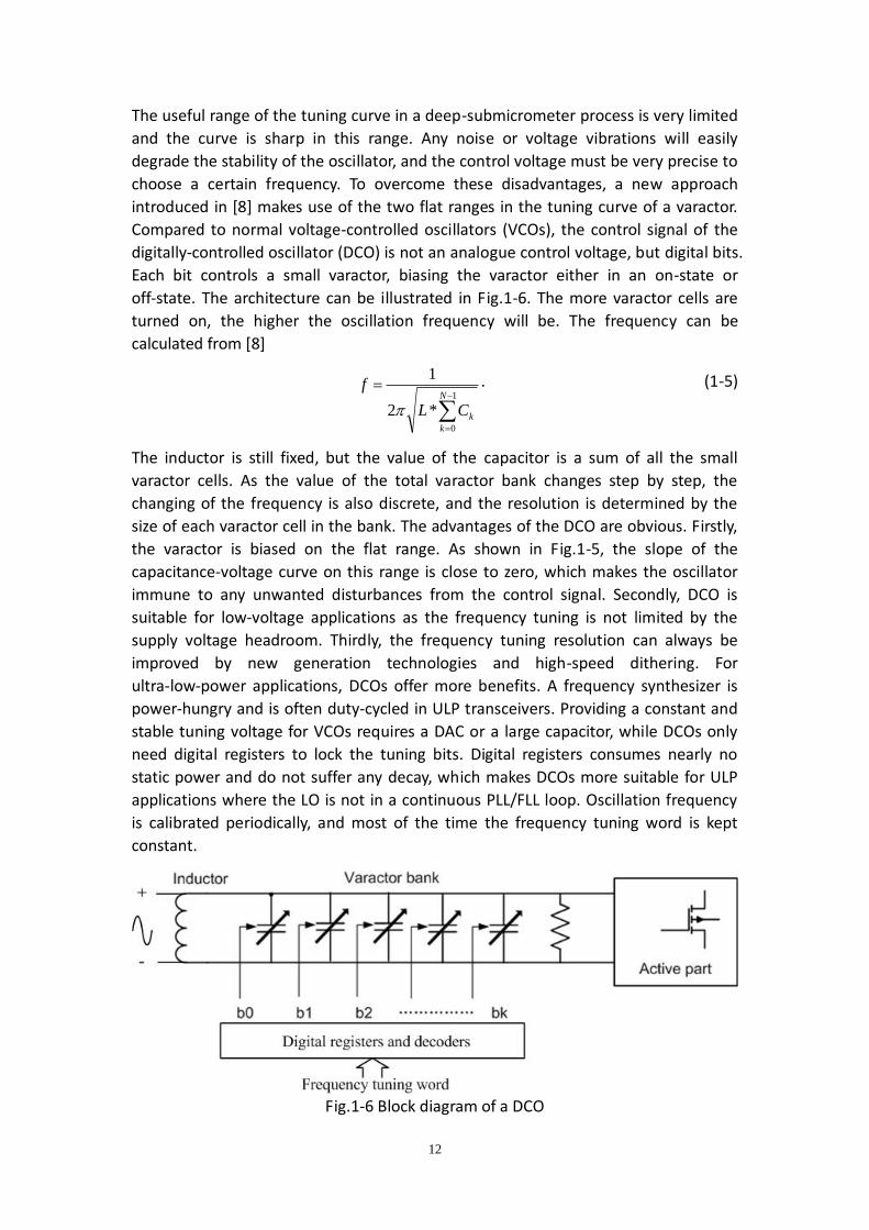
To define a suitable output power level for the transmitter, the link budget should be
calculated. The sensitivity of the receiver is already shown in Fig.2-3. The path loss is
estimated by using two general models.
d
c
fdPL fs
4log10 10 . (2-1)
Eqn.2-1 [4] is used for free-space path loss calculation. Free space means there is a
light-of-sight (LOS) path between the transmitter and receiver without any obstacle
to cause absorption and reflection. The distance from the transmitter to the receiver
is d , dPL is the path loss in dB, f is the carrier frequency and c is the speed
of light. fs is an attenuation coefficient and equals to 2 for free-space situation.
The path loss curves for different frequency bands are illustrated in Fig.2-4.
Fig.2-4 Free-space light-of-sight path loss curves for different frequency bands
An empirical model used in [4] is more practical for indoor applications, which is
given Eqn.2-2. Within 8 meters, the path loss is estimated as free-space propagation,
but electromagnetic waves attenuate more rapidly when the distance exceeds 8
meters. The path loss curves for this model are plotted in Fig.2-5.

20
md
dPL
mddPL
dPL8
8log108log10)1(
8log10)1(
108101
101
(2-2)
3.3,2,
4log101 81101
c
fPL .
The output power of the transmitter should be large enough to overcome the path
loss and make sure that the signal strength at the input of the receiver is above the
receiver’s sensitivity. The required output power outP can be calculated as
Rxoutreceived SdPLPP )( . (2-3)
receivedP is the received power by the receiver, and RxS is the sensitivity of the receiver.
Fig.2-5 Indoor path loss curves for different frequency bands
As the transmitter is more power-hungry than the receiver, the receiver should be set
to the highest sensitivity mode in order to maintain a certain communication
distance while minimizing the overall power consumption of the transceiver. The
power consumption of the receiver is a little higher, but it is more efficient than
increasing the output power of the transmitter. The more power delivered to the
antenna, the more power consumed by the power amplifier which has an efficiency
far below 100%. As shown in Fig.2-3, the sensitivity is improved about 8dB by
increasing the power consumption from 101uW to 123uW. For the transmitter, such
a slight change in power consumption hardly increases the output power.

21
Based on the link budget analysis above for this transmitter, the output power is set
to -10dBm, which makes sure that the transceiver can cover many different
applications. If the sensitivity is -83dBm at a moderate data rate of 10kbps, this
transceiver can support an outdoor application in the range of 140m and an indoor
application in the range of 40m. Illustrated in Fig.2-6, this is sufficient for common
applications such as smart keys and industrial control.
Fig.2-6 Received signal strength versus distance
Table.2-2 Design specification of this transmitter
Power consumption <1mW
modulation OOK
Frequency band 780-950MHz
Output power >-10dBm
Data rate >100kbps
D. Conclusions
The design specification is summarized in Table.2-2. For event-driven applications,
the power consumption should be as low as possible, so OOK modulation is chosen
as its nature advantage for low power applications. The transmitter works in the
sub-GHz ISM frequency bands, achieving a balance between cost, power
consumption and flexibility. To cover many different application situations, the

22
output power of the transmitter is aimed at -10dBm. In a transceiver, the data rate is
dominated mainly by the receiver, so the transmitter should at least support the
highest data rate desired for the receiver.
2.2 State-of-the-art designs
Before introducing the proposed architecture, this section surveys some
state-of-the-art designs that have similar design specification. Minimizing the power
consumption of the carrier generation in a ULP transmitter discussed in Section 1.2 is
one of the most challenging design targets, so the various solutions for carrier
generation are highlighted in the following analysis.
A. Direct transmitting architecture [5]
In [5], a 400MHz OOK transmitter is designed for a wireless capsule endoscope. The
transmitter architecture is shown in Fig.2-7. This transmitter is simply composed of
an LC tank oscillator and a buffer-like power amplifier. To reduce power
consumption, the oscillator is biased as a current reuse topology. The oscillator
drives the power amplifier directly and the OOK modulation is applied by turning on
and off the entire transmitter. Some switches are added to improve the data rate by
reducing the rise and decay time of the OOK signals. As the oscillator is free running,
the precision of the carrier cannot be guaranteed. Since there is no buffer between
the oscillator and the power amplifier, any disturbances on the amplifier or even the
antenna can directly affect the oscillating frequency. This simple architecture
achieves low power consumption at the cost of frequency stability and output power
adjustability, which limits its applications.
Fig.2-7 A 440MHz OOK transmitter [5]
23
Table.2-3 Performance summary of the transmitter in [5]
Frequency Modulation Max output
power
Average power
consumption
Data rate Efficiency
440MHz OOK 0dBm 2.58mW 40Mbps 19.3%
B. SAW stabilized architecture [6]
To achieve both high performance and low power consumption, many researchers
make use of high-Q high-precision RF resonators to generate carrier signals. In [6], a
complete transceiver for wireless sensor networks (WSN) is published. It works in
the 902-928MHz ISM frequency bands and uses OOK modulation. The receiver
adopts an envelope detector to demodulate the OOK signals. In the transmitter, a
surface acoustic wave (SAW) stabilized Colpitts oscillator is used for carrier
generation, and two differential pairs in cascade serve as a buffer to drive the power
amplifier. Modulation is applied by turning on and off the final two amplifier stages.
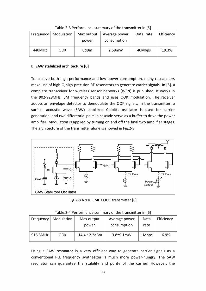
The architecture of the transmitter alone is showed in Fig.2-8.
Fig.2-8 A 916.5MHz OOK transmitter [6]
Table.2-4 Performance summary of the transmitter in [6]
Frequency Modulation Max output
power
Average power
consumption
Data
rate
Efficiency
916.5MHz OOK -14.4~-2.2dBm 3.8~9.1mW 1Mbps 6.9%
Using a SAW resonator is a very efficient way to generate carrier signals as a
conventional PLL frequency synthesizer is much more power-hungry. The SAW
resonator can guarantee the stability and purity of the carrier. However, the

24
disadvantage is that the center frequency is fixed and cannot be tuned. For WSN
applications, nodes must therefore use the time-division multiplexing technique to
share the same channel. In this SAW stabilized oscillator, the SAW resonator only
acts as a filter to close the feedback loop in the oscillator; the oscillator itself is a
Colpitts oscillator based on a LC tank. The power consumption mainly depends on
the loss of the LC tank, and the high-Q SAW resonator doesn’t help to reduce power
consumption. Furthermore, the phase noise of a high-Q crystal resonator oscillator is
normally lower than -130dBc@1MHz, but the phase noise of this oscillator is only
-114.3dBc@MHz. The SAW resonator in this architecture hardly improves the
frequency purity, and the LC tank still dominates the overall performance of the
oscillator.
C. Injection-locked architecture [7]
The transmitter from [7] also uses a high-Q RF resonator to implement the carrier
generation for a 1.9GHz OOK transmitter. The architecture is shown in Fig.2-9. A
Pierce oscillator based on a film bulk acoustic resonator (FBAR) generates stable but
weak carrier signals. A power oscillator directly drives the antenna, and it is injection
locked by the FBAR oscillator so its output signals are as precise as the output of the
FBAR oscillator. Compared with the SAW stabilized oscillator in [6], this oscillator has
a different topology. It directly uses the High-Q component as a resonating tank but
not as an additional filter. This scheme fully exploits the advantage of the high-Q
resonator, providing precise carrier signals very efficiently. However, in order to lock
the power oscillator, the free running frequency of the power oscillator should be
close to the FBAR resonating frequency. Reliable injection-locking depends on the
power strength of the injection signal and the Q-factor of the power oscillator. An
additional frequency calibration loop is still needed to tune the power oscillator to
make sure the free running frequency is in the locking range. Actually, the
injection-locked technique relaxes the precision requirement for frequency
synthesizer but does not completely get rid of it. Also, the lock-in time depends on
the frequency difference, the power strength of the injection signal and the Q-factor
of the power oscillator. There are complex trade-offs between power consumption,
data rate and other design specifications, which makes it difficult to optimize the
performance overall. Later, the author of [7] published a new transmitter in [8]. A
FBAR oscillator is still used, but the transmitter is not based on the injection-locked
technique. The oscillator directly drives a high-efficiency power amplifier, eliminating
the need for an additional frequency calibration loop.

25
Fig.2-9 An injection-locked transmitter [7]
Table.2-5 Performance summary of the transmitter in [7]
Frequency Modulation Max output
power
Average power
consumption
Data
rate
Efficiency
1900MHz OOK 0dBm 1.8mW 156kbps 28%
D. Current-reuse architecture [9]
A complete FSK transceiver operating at 900MHz is described in [9]. Fig.2-10 shows
its block digram. Different with [6] and [7], a frequency-locked loop (FLL) based on
digital counters is implemented to stabilize the oscillating frequency of a DCO. For
FSK the phase of the carrier does not contain any information, so an FLL is precise
enough. Compared with a phase-locked loop (PLL), the FLL consumes less power as
its architecture is simpler. The LC oscillator is digitally-controlled, which makes it
compatible with the digital FLL. A high-Q off-chip inductor is used to achieve low
power operation. As the supply voltage is as high as 3V, the bias current of the DCO
is reused to bias all the other circuit blocks to further reduce power consumption. A
disadvantage of the current reuse topology is unwanted coupling via the power
supply between different circuit blocks. Compared with OOK modulation, FSK
consumes more power in both the transmitter and the receiver. This is because FSK
modulation needs the power amplifier to be always on, and demodulating FSK
signals needs the help of an RF local oscillator in the receiver.

26
Fig.2-10 A 900MHz transceiver [9]
Table.2-6 Performance summary of the transmitter in [9] (*transmitter only)
Frequency Modulation Max output
power
Average power
consumption*
Data rate Efficiency
900MHz OOK -6dBm 1.3mW 20kbps 19%
2.3 Proposed architecture
After summarizing some state-of-the-art designs in the last section, two potential
solutions for this transmitter are proposed. Further investigation on power
consumption shows that the RF resonator based solution is not feasible for the
design specifications adopted in this works.
2.3.1 Potential solutions
Event-driven transmitters do not need to support high data rate on a very long
communication span, but the requirement for power consumption is still challenging.
Compared to traditional transmitter architectures, the event-driven transmitter
needs to be simplified, and some performance is sacrificed for power consumption.
For the carrier generation, a traditional frequency synthesizer is not necessary. But
open loop operation hardly guarantees reliable performance in most applications
due to the inaccuracy of normal passive components. To overcome this disadvantage,
two potential solutions are conduced here.

27
Fig.2-11 RF-resonator based architecture
One is making use of a high-Q, high-precision RF resonator. Such a circuit is shown in
Fig.2-11. An RF resonator oscillator can provide precise carrier signals, and the OOK
modulation is directly applied to the power amplifier (PA). The buffer in between is
for isolation purposes, so that the power amplifier does not affect the operation of
the oscillator. The input impedance of the buffer depends on its status. To minimize
the loading effect and achieve the best stability, the buffer is always on.
Fig.2-12 DCO based architecture
The other solution uses a DCO combined with a simply frequency calibration loop to
generate carrier signals. The architecture is showed in Fig.2-12. The buffer stage and
the power amplifier (PA) is the same as the first architecture in Fig.2-11. A digital
frequency calibration block is used to tune the center frequency of the DCO. Taking
advantage of the digital operation, the calibration block can be duty cycled to further
save power. When starting to transmit, the calibration block tunes the oscillator to
the desired frequency and then goes to standby mode. Depending on the
requirements for the specific application, the calibration block wakes-up periodically
to correct the carrier frequency.

28
2.3.2 Power consumption investigation
Using RF resonators, the center frequency is fixed. Time-division multiplexing must
be applied to make sure that many transceivers can share the same channel. On the
other hand, using a frequency calibration loop increases the complexity of the
transmitter. As will be shown later, further investigation of the power consumption
for a SAW oscillator shows that the RF resonator based transmitter is not feasible for
the design specifications adopted in this works.
The power consumption of an RF resonator oscillator can be estimated using a
method introduced in [10]. Given the equivalent electrical model of the RF resonator,
the required transconductance for the active part can be calculated, and then the
power consumption is estimated.
A commercial 915MHz SAW resonator (EPCOS R973) is chosen for the following
estimation. From its datasheet [11], an equivalent electrical model is shown in
Fig.2-13.
Fig.2-13 Equivalent electrical model Fig.2-14 SAW based pierce oscillator
This RF resonator is used in a Pierce oscillator, which is illustrated in Fig.2-14 (bias is
not shown completely). Z1 and Z2 are the impedance values of the two capacitors,
and Zsaw represents the equivalent impedance value of the SAW resonator.
Assuming that the bias source and the transistor are ideal, the loop gain can be
calculated as
SAW
m
ZZZ
ZZgG
21
21 . (2-4)

29
To maintain stable oscillation, the Barkhausen criteria should be met:
0
1
G
G. (2-5)
The absolute value of the loop gain G should be larger than one to start oscillation.
When the oscillation is stable, it should be equal to unity and the phase shift G
must be zero degree. From Eqn.2-4 and Eqn.2-5, the required transconductance can
be calculated:
2))(Im(
)Re(4
SAW
SAWm
Z
Zg . (2-6)
Fig.2-15 The required transconductance versus oscillation frequency
The required transconductance versus oscillation frequency is plotted in Fig.2-15.
The two peaks are due to the series and parallel resonances of the SAW resonator.
Normally, the oscillator operates at a frequency between them. The minimum
transconductance required for stable oscillation is 40.7mS. It happens when the
oscillation frequency is tuned to be 915.1MHz by carefully choosing the value of the
two capacitors. Assuming that the transconductance efficiency of the transistor
biasm IG is 20, which is almost the maximum value under weak inversion bias
condition in modern IC manufacturing technology, the required bias current is about
2mA. If the supply voltage is 1V, the power consumption of the oscillator is as high as
Series resonance Parallel resonance
Minimum Gm

30
2mW. In practical implementation, the power consumption will be much higher, due
to the parasitic capacitors of the transistor and its output resistor. Considering the
output power of the transmitter is only -10dBm, an SAW oscillator consuming 2mW
is hardly satisfactory.
At first sight, the high power consumption of the SAW resonator oscillator seems to
conflict with the high-Q performance of the SAW resonator. But it can be explained
using a more complete model in [12]. In this model, the required transconductance
can be expressed as
21
2
1221 )(
CC
CCCCCC
QCg
pp
s
m
. (2-7)
It is difficult to directly calculate Gm using Eqn.2-7, as the values of C1 and C2 cannot
be chosen freely. But some qualitative conclusions can be drawn. The required
transconductance not only depends on the Q-factor of the resonator but also
depends on the operation frequency and the values of Cs and Cp. The highest
resonating frequency that a SAW device can achieve is on the order of 915MHz. For
a SAW resonator at 915MHz, Cs is only 1.415fF while Cp is as large as 1.8pF. The
Q-factor of such a SAW resonator can be as high as a few thousands, but this
advantage is counteracted by the high operating frequency, small Cs and big Cp.
2.3.1 Conclusions
Two potential solutions are shown in this section; one based on an RF resonator to
generate carrier, the other with a frequency calibration loop and a
digitally-controlled oscillator. Limited by the performance of the SAW resonator at
915MHz, carrier generation using a SAW oscillator consumes unaffordable power for
ULP circuits. Considering the desired specifications for this project, the DCO-based
architecture is more suitable. Using a high-Q SMD inductor, the DCO can achieve
very low power consumption. The frequency calibration loop can be duty cycled so
that the average power consumption is also very low. Before going into the design
details of the DCO in next chapter, the proposed architecture is summarized.
The proposed event-driven transmitter is shown in Fig.2-16. For the first prototype
of this transmitter, not all of the circuit blocks are implemented on-chip. The
frequency calibration and modulation will be implemented in a FPGA, while all the
critical blocks including the complete RF front-end are integrated on chip. The DCO
uses 16-bit control signals to tune the frequency, making sure that it can cover the
required frequency bands. The buffer isolates the DCO and all other analog and RF

31
blocks to improve the stability of the DCO. A decoder is added between the DCO and
the FPGA to simplify the interconnection and also to isolate the noisy digital circuits
from the RF circuits. The high-frequency divider is critical in a frequency calibration
loop, so it is also implemented on chip. The FPGA can process the low-frequency
signals, which still contain the frequency information of the DCO. An amplitude
swing detection block followed by an 8-bit ADC is also driven by the buffer. The
swing information is used to change the bias of the DCO, making sure that the
oscillator has the right amplitude and that the PA has required driving power. The
gain of the PA is also tunable, so that it can support not only OOK, but also other ASK
modulations. Another advantage of tunable gain is that the output power can be
changed for different application environments to optimize the power consumption.
The blue wire fame includes all the circuit blocks on chip. The carrier generation part
is highlighted by the red wire fame, and will be analyzed in the next chapter.
Fig.2-16 The complete circuit diagram for the first tape-out of the event-driven
transmitter
2.4 Conclusions
In this chapter, the design specification of the event-driven transmitter is firstly
defined. OOK modulation is applied and the operation frequency is chosen to be the
902-928MHz ISM band. After a complete link-budget calculation, the output power
of the event-driven transmitter is set to be larger than -10dBm to support both
out-door and in-door applications. Secondly, the architecture of this transmitter is
discussed. Some state-of-the-art designs are summarized and evaluated, and two
potential solutions are presented. After investigating their power consumption, the
DCO based architecture is chosen and analyzed in detail.

32
References
[1] X. Huang, S. Rampu, X. Wang, G. Dolmans, and H. De Groot. “A 2.4GHz/915MHz
51µW wake-up receiver with offset and noise suppression”. IEEE International
Solid-State Circuits Conference ISSCC, pp.222-223, Feb. 2001.
[2] Yan Zhang. “WuRx system evaluation”. IMEC-NL. Internal report. 05-2011.
[3] “ISM Bands”. Wikipedia. Retrieved 04-2011, from
http://en.wikipedia.org/wiki/ISM_band
[4] Anuj Batra, Marco Hernandez, Mark Dawkins, Srinath Hosur, Jung-Hwan Hwang,
Daniel Lewis, Seung-Hoon Park, Kenichi Takizawa. “TG6 Coexistence Assurance
Document”. IEEE P802.15 Working Group for Wireless Personal Area Networks
(WPANs), March 2011.
[5] Jiho Ryu, Minchul Kim, Jaechum Lee, Byung-Sung Kim, Moon-Que Lee, Sangwook
Nam. “Low Power OOK Transmitter for Wireless Capsule Endoscope”. Microwave
Symposium IEEE/MTT-S International, pp. 855-858, Jun. 2007.
[6] D.C. Daly, Anantha P. Chandrakasan. "An Energy-Efficient OOK Transceiver for
Wireless Sensor Networks". IEEE Journal of Solid-State Circuits, Vol.42, No.5,
pp.1003-1011, May. 2007.
[7] Y.H. Chee, Ali M. Niknejad, Jan M. Rabaey. "An Ultra-Low-Power Injection Locked
Transmitter for Wireless Sensor Networks". IEEE Journal of Solid-State Circuits,
Vol.41, No.8, pp.1740-1748, Aug. 2006.
[8] Y.H. Chee, A.M. Niknejad, J. Rabaey. "A 46% Efficient 0.8dBm Transmitter for
Wireless Sensor Networks". VLSI Symposium Dig. Tech. Papers, pp.43-44, 2006.
[9] A. Molnar, B. Lu, S. Lanzisera, B.W. Cook, and K.S.J. Pister. “An Ultra-Low Power
900 MHz RF Transceiver for Wireless Sensor Networks”. IEEE Custom Integrated
Circuits Conference, pp. 401-404, 2004.
[10] Louis-Francois Tanguay and Mohamad Sawan. “Low Power SAW-Based
Oscillator for an Implantable Multisensor Microsystem”. Asia Pacific Conference on
Circuits and Systems, pp. 494-497, 2006.

33
[11] Datasheet. EPCOS. Retrieved 2009, from
http://www.epcos.com/inf/40/ds/ae/R973.pdf
[12] E. A. Vittoz, M. G. R. Degrauwe, and S. Bitz. "High-performance crystal oscillator
circuits: theory and application". IEEE Journal of Solid-State Circuits, Vol. 23, pp. 774,
1988.

34
Chapter 3
Oscillator design
For event-driven communication, the transmitter should be optimized for the lowest
power consumption. Under the condition of ultra-low-power, carrier generation is
critical to achieve a high overall efficiency. A DCO circuit for an event-driven
transmitter is proposed in the last chapter. This chapter will concentrate on the
design of an ultra-low-power digitally-controlled oscillator. General design
considerations are first discussed, and then each block of the DCO is analyzed in
detail. To optimize power consumption, frequency tuning and phase noise, the
circuit topologies are carefully chosen and different design techniques are applied.
The physical layout is also emphasized as it directly affects the performance of the
DCO. Finally, the simulation results are summarized.
3.1 General considerations
This digitally-controlled oscillator is designed to integrate into an event-driven
transmitter for carrier generation. It is implemented in TSMC’s 90nm CMOS
technology, and uses only one SMD component. Although a supply voltage close to
1V helps to reduce power consumption, the supply voltage is limited by the
threshold voltage of the transistor in available process technology. Considering the
threshold voltage of a normal NMOS transistor in TSMC’s 90nm CMOS technology is
around 450mV, the supply voltage of this oscillator is chosen to be 1V making sure
that at least 3 transistors can be cascoded. The LC-oscillator operation was
introduced briefly in Chapter 1. To fulfill the system requirements for the
event-driven transmitter, power consumption, frequency tuning and phase noise are
three of the most important design parameters. Before going into the circuit level
design, they are first discussed and some general conclusions are drawn.
3.1.1 Power consumption
As discussed in Chapter 2, the desired output power of the event-driven transmitter
is -10dBm, and the total power consumption should be less than 1mW. Given that
the drain efficiency of the power amplifier is 30%, which is a reasonable estimate for
class-AB power amplifiers, 400mW is reserved for the power amplifier. In order to
make sure that the overall efficiency of the transmitter is not reduced by the pre-PA

35
stage, the power consumption of the oscillator should be less than 200mW. Then
there is still margin to implement the oscillator buffer and frequency divider, which
is shown in Fig.2-16.
The first step to achieve the ultra-low-power performance is to minimize the loss in
the LC tank. The loss of the LC tank is quantified by the quality factor:
dissipatedpowerAverage
storedEnergyQT . (3-1)
Fig.3-1 Model of a LC oscillator
Both the inductor and the capacitor are disspate energy. Their losses can be
modeled by a parallel resistor, as shown in Fig.3-1. The quality factor of the inductor
( LQ ) and the capacitor ( CQ ) can be quickly expressed as
., CCL
L CRQL
RQ
(3-2)
Then the quality factor of the LC tank can be deduced as
CLCLCL
CL
T QQCRR
L
CRCRCV
R
V
R
V
Q
11111
2
1
2211
2
22
. (3-3)
The oscillation amplitude V means the peak voltage of the LC resonance tank.
Eqn.3-3 shows that the quality factor of the LC tank is dominated by the component
which has a lower quality factor. In the TSMC’s 90nm CMOS technology, the quality
factor of a MOS varactor is higher than 150 while the quality factor of an on-chip
spiral inductor is only around 15 at 900MHz, the on-chip tank will have a Q-factor of
around 15. On the other hand, an off-chip inductor can have a quality factor of 50 or
even higher. Then an off-chip inductor (Murata LQW15A series) is used in this design,
which has a quality factor of 70 at 900MHz. However, using an off-chip inductor

36
increases the design difficulty. Metal connections between the chip and the inductor
include the bondwires, the leadframe of the package and the PCB mounting. The
parasitic effects from these components must be taken into account when
optimizing the frequency tuning.
Besides the quality factor, the inductance also affects the power loss in the LC tank.
As shown in Eqn.3-2, the equivalent parallel resistor is proportional to the inductor.
If the quality factor is the same, a larger inductance implies lower power loss.
However, as the resonant frequency of the LC tank is inversely proportional to the
product of the inductance and the capacitance, a large inductance will limit the value
of the capacitor, making it difficult to implement the varactor bank. For example, a
20nH inductor requires only 1.5pF total capacitance to resonate at 915MHz.
Considering that a bondpad (75um×75um) can contribute 230fF parasitic
capacitance, it is difficult to implement the varactor bank using the 1.5pF margin and
taking all of the parasitics capacitance into account. Therefore, a 12nH off-chip
inductor is used, leaving enough capacitance space to design the varactor bank,
including all the circuit parasitics.
The design of the active part of the DCO is the second key point to reduce power
consumption. The active part generates alternating current from the DC supply to
overcome the loss in the LC tank. It can be simply modeled as a negative resistor, as
shown in Fig.3-1. To establish and maintain a stable oscillation, the absolute value of
the equivalent negative resistor should be smaller or equal to the equivalent parallel
resistor of the LC tank [1]. How to achieve this requirement while consuming less DC
current is the design challenge and will be analyzed in Section 3.2.
3.1.2 Frequency tuning
Changing the digital control word of the DCO will change the total capacitance of the
varactor bank step by step and then change the oscillation frequency discretely.
Although each LSB cell in the varactor bank has the same value, due to the nonlinear
transfer function shown in Eqn.3-4, the frequency steps are not constant across the
entire tuning range. The frequency resolution is defined by the maximum frequency
step. This happens at the highest frequency point, because a change of the varactor
bank is more significant when the bank has a smaller value. To guarantee that the
oscillation frequency can be close enough to a specified frequency within the whole
frequency band, the resolution is made smaller than 100kHz for this design.

37
).10(22
1fFC
C
Cff
LCf
(3-4)
Another problem about frequency tuning is the tuning range. This oscillator is aimed
to work in the 902-928MHz ISM frequency band (making that by changing the value
of the off-chip inductor, it can also support sub-GHz ISM bands). Its center frequency
should be tunable to cover the entire 902-928MHz frequency band. Although the
bandwidth is only 26MHz, the practical tuning range must be much wider, because
the tolerance in the value of the passive components. The off-chip inductor has a
tolerance of ±5%, and the parasitic inductance from the bondwire is 2.7nH
(2.7mm×1nH/mm) with a spread of ±20%. The parasitic inductance and capacitance
from the leadframe and PCB mounting are also quite uncertain. As the off-chip
inductor is much larger than the parasitic inductance from all of the metal
connections, in the total lumped inductance an estimated total spread of ±10% is
assumed to be large enough to cover the anticipated space. The tuning range of the
oscillator must be larger than 20% for practical use.
The varactor bank is implemented for frequency tuning. Wide tuning range and high
frequency resolution are the design tasks. Considering Eqn.3-4, these two targets
seem contradict each other. If the total number of control bits are fixed, wider
tuning range requires maximizing the capacitance step, while higher resolution
requires minimizing it. To achieve wide tuning range and high resolution at the same
time, two sub varactor banks are designed to optimize them respectively. The coarse
bank is for wide tuning range. The desired frequency must be covered, so C in
each step of the coarse bank must be large enough. The fine bank is for frequency
resolution. The capacitance step C should be minimized, so the oscillation
frequency can be close enough to a specified frequency within the whole tuning
range. The design of the two varactor banks will be discussed further in Section 3.3.
3.1.3 Phase noise
Phase noise is an important performance parameter of an oscillator. The output
signal of any practical oscillator is not a perfect sine wave. In the frequency domain,
as shown in Fig.3-2, the spectrum of the output signal is not a single impulse but
looks like a “skirt” shape around the oscillation frequency [1]. The phase noise is
defined as the relative noise power to the carrier within a unit bandwidth at an
offset from the center frequency. Phase noise of a signal from a transmitter may
corrupt an adjacent signal (in nearby channel). For event-driven communication, as
the output power of the transmitter is quite low, this effect is not very critical.

38
However, lower phase noise is always desirable to improve spectrum efficiency. For
this design, the phase noise at 915MHz should be lower than -120dBc/Hz at 1MHz
offset, which is a state-of-the-art value in CMOS technology. Based on the model in
[2], there are many sources in a LC tank oscillator that can generate phase noise,
such as the bias of the active part and the varactor banks. So optimizing the phase
noise performance involves each part of the circuit design.
Fig.3-2 Phase noise of a practical oscillator
3.1.4 Conclusions
Using a high-Q off-chip inductor, the loss of the LC tank is reduced. To further
optimize power consumption, the active part should be carefully designed.
Frequency tuning is achieved by two varactor banks. Wide tuning range and high
resolution are two design challenges. All the parasitic effects from the metal
connection between the off-chip inductor and the chip will affect the resonant
frequency and must be taken into account when designing the varactor banks.
Optimizing phase noise performance is also challenging as it involves each part of the
oscillator. Based on the above analyses, the design specification of this oscillator is
summarized in Table.3-1.

39
Table.3-1 Design summary
Technology TSMC’s 90nm CMOS Technology
SMD component One SMD inductor (LQW15AN12NG00)
Supply voltage 1V
Power consumption <200uW
Center frequency 915MHz
Tuning range >20%
Frequency resolution <100kHz
Phase noise <-120dBc/Hz@1MHz
3.2 Active part
The circuit topology of the active part is firstly discussed. Then the transistor sizing
and biasing are analyzed respectively. Finally, the active-part design is summarized.
3.2.1 Circuit topology
There are many topologies that can be used to implement the active part. Their
operating principles are all the same, establishing a positive feedback to inject
alternating current into the LC tank and overcome the loss. Three common
topologies are shown in Fig.3-3.
(a) Colpitts (b) Single pair (c) Push-pull
Fig.3-3 Common topologies of a LC oscillator

40
A Colpitts topology is shown in Fig.3-3 (a). It is popular in the past as it only needs
one transistor. The feedback signal returns to the source by using a tapped capacitor
transformer. The source impedance 1/Gm (Gm is the transconductance) is also
transformed back to load the LC tank, so the total equivalent parallel resistor is
)(1
21
1
2tanCC
Cn
GnRR
m
kp
. (3-5)
Generating positive feedback to the source increases the overall loss in the circuit,
some power is wasted and the efficiency is low. So the Colpitts is not very feasible.
Applying the feedback signal to the gate needs additional phase shift to guarantee a
positive loop, but it presents higher loading impedance in parallel with the LC tank so
the loss is reduced. This idea leads to the single NMOS pair topology shown in Fig.3-3
(b). The two transistors act as an active buffer between the other’s drain and gate
terminals. Looking at the LC tank, the real part of the impedance between the drain
terminals are equivalent to a negative resistor:
m
gleG
R2
sin
. (3-6)
The principle of the push-pull topology in Fig.3-3 (c) is the same as the single pair
topology, a PMOS pair is stacked onto the NMOS pair and the bias current is reused.
Assuming the PMOS transistors has the same transconductance with the NMOS
transistors, the equivalent negative resistor can be calculated as
m
pullpushG
R1
. (3-7)
The absolute value of the negative resistor must be smaller than the equivalent
parallel resistor of the LC tank to sustain oscillation. As the transconductance of a
transistor is proportional to its bias current, the push-pull topology can generate the
same negative resistor while only consuming half of the bias current compared with
the single NMOS pair topology. Although the single NMOS pair requires only half of
the supply voltage, as the supply voltage is fixed at 1V for this design, half bias
current means half power consumption, so the push-pull topology requires lower
power from 1V supply. However, the output amplitude of the push-pull topology is
limited to the supply voltage, while the single NMOS pair topology can reach twice of
the supply voltage in theory. For this design, a differential output swing of 500mV is
enough to drive the next stage buffer, which is not difficult to achieve from the
push-pull topology. With regard of phase noise performance, if the output amplitude
is the same, these two topologies have almost the same phase noise level based on
the Leeson’s model [2]. This is demonstrated by measurement results in [3]. Another
difference between these two topologies lies in the DC bias. The single pair topology

41
requires a tap in the middle of the inductor to feed DC current, but this is difficult to
be implemented by using a single off-chip inductor.
Base on the above analyses, the push-pull topology is chosen for this design as the
power consumption can be reduced and its phase noise performance is also good
enough. A disadvantage of the push-pull topology is that the DC voltage on the LC
tank depends on the bias current and the working status of the four transistors. This
makes the bias of the varactor banks more complex as a stable bias voltage should
be provided by additional circuit blocks. The bias of the varactor banks will be
discussed later.
3.2.2 Transistor sizing
After choosing the circuit topology, the second step is to size the transistors properly.
The design goal is to generate enough transconductance when reducing the bias
current. All the four transistors are biased in the weak inversion region to achieve
high transconductance efficiency biasm IG .
In the TSMC’s 90nm CMOS technology, the drain current (Id) versus gate-source
voltage (Vgs) curve of a NMOS transistor (Width=2um, Finger=10, Length=100nm) is
shown in Fig.3-4. The transconductance efficiency versus bias current is also plotted.
When the bias current is low, the transistor works in the weak inversion region and
the current is exponential proportional to the gate-source voltage. When the
gate-source voltage reaches the threshold voltage (440mV) and exceeds it, the
working status moves from the moderate into the strong inversion region. The slope
of the Id-Vgs curve is smaller and the transconductance efficiency drops quickly.
Obviously, if the bias current is the same, increasing the width of the transistor to
make it work in the weak or moderate inversion region can achieve better efficiency.
As all the parasitic capacitance from the transistors is absorbed into the resonant
tank, the cut-off frequency is not important here. However, if all four transistors are
biased deep in the weak inversion region, the width of the transistors is very large
and the total parasitic capacitance is huge. This will increase the total constant
capacitance in the tank and limit the margin for implementing the varactor banks.
Biasing the transistors in the weak inversion region but close to the moderate
inversion region achieves a better trade-off between efficiency and parasitic
capacitance. So the length of the transistors is set as the minimum value (100nm) in
library, and the width is chosen to make the transistor working in the desirable
region. For the NMOS transistors, the width is 2um and the number of fingers is 20.

42
As the NMOS transistors’ carrier mobility is roughly twice of the PMOS transistors’,
the total width of PMOS transistors are double to make an equal transconductance.
This offers better symmetry of rising and falling time, which results in a smaller 1/f
phase noise corner [2].
Fig.3-4 (a) Id-Vgs curve of a NMOS transistor (b) Transconductance efficiency
3.2.3 Biasing
A current mirror is often used to provide tunable bias current. Phase noise is the
most important design specification here. The 1/f noise generated by a MOS
transistor can be calculated as [2]
2
22
ker
ox
mflic
WLC
KGi . (3-8)
K is a device-specific constant. Normally PMOS transistors show a smaller K than
NMOS transistors, so a PMOS current mirror is used. Eqn.3-8 also shows that
reducing the flicker noise requires a large transistor area with a small
transconductance. As shown in Fig.3-5, to fulfill these requirements, the length of
the PMOS transistors is 0.24um while the total width is 20um.
Fig.3-5 Bias current mirror
Gate-source voltage (V) Bias current (uA)
Bias current (A) Transconductance efficiency

43
To further reduce the noise from transistor Q2, a 20pF decoupling capacitor is added
at its gate. The noise from the bias current and Q2, especially high frequency noise,
is filtered out. The capacitance value depends on the available layout area left for it,
but a large decoupling capacitor also slows down the start-up time of the oscillation
as the charging time of it is longer.
3.2.4 Conclusions
The circuit diagram of the active part is shown in Fig.3-6. The push-pull topology is
applied as its power efficiency is higher than other topologies. The four transistors
are biased in weak inversion region to further improve efficiency by generating
larger transconductance under the same bias condition. A PMOS current mirror is
used to bias the active part. A large decoupling capacitor is added as a low pass filter
to reduce phase noise from the bias current mirror. The design details are discussed
as follows.
Fig.3-6 Circuit diagram of the DCO
3.3 Varactor banks
The varactor bank is the most complicated block in a DCO. Two sub banks are
implemented to achieve wide tuning range and high frequency resolution
respectively. The architecture of the two varactor banks are the same, the only
difference lies in the varactor size in each LSB cell. The varactors in the coarse bank
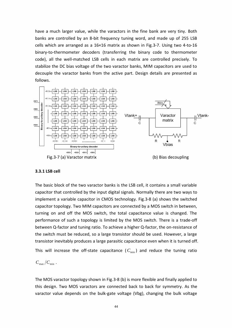
44
have a much larger value, while the varactors in the fine bank are very tiny. Both
banks are controlled by an 8-bit frequency tuning word, and made up of 255 LSB
cells which are arranged as a 16×16 matrix as shown in Fig.3-7. Using two 4-to-16
binary-to-thermometer decoders (transferring the binary code to thermometer
code), all the well-matched LSB cells in each matrix are controlled precisely. To
stabilize the DC bias voltage of the two varactor banks, MIM capacitors are used to
decouple the varactor banks from the active part. Design details are presented as
follows.
Fig.3-7 (a) Varactor matrix (b) Bias decoupling
3.3.1 LSB cell
The basic block of the two varactor banks is the LSB cell, it contains a small variable
capacitor that controlled by the input digital signals. Normally there are two ways to
implement a variable capacitor in CMOS technology. Fig.3-8 (a) shows the switched
capacitor topology. Two MIM capacitors are connected by a MOS switch in between,
turning on and off the MOS switch, the total capacitance value is changed. The
performance of such a topology is limited by the MOS switch. There is a trade-off
between Q-factor and tuning ratio. To achieve a higher Q-factor, the on-resistance of
the switch must be reduced, so a large transistor should be used. However, a large
transistor inevitably produces a large parasitic capacitance even when it is turned off.
This will increase the off-state capacitance ( minC ) and reduce the tuning ratio
minmax CC .
The MOS varactor topology shown in Fig.3-8 (b) is more flexible and finally applied to
this design. Two MOS varactors are connected back to back for symmetry. As the
varactor value depends on the bulk-gate voltage (Vbg), changing the bulk voltage

45
while keeping the gate voltage constant will change the varactor value directly.
There are no additional components that limit the overall performance. Q-factor and
tuning ratio depend only on the varactors themselves. For the coarse bank, a wide
tuning range is the foremost design task. The MOS varactors in the TSMC’s library
are used as the capacitance step C (11.6fF) and tuning ratio minmax CC (3.7) are
large enough. For the fine bank, the change in capacitance at each step C should
be on the order of 100aF. Therefore, normal deep N-well NMOS transistors are
chosen to implement the MOS varactor pair. The deep N-well structure helps to
reduce noise coupling from the substrate. NMOS but rather than PMOS are used
because its voltage-to-capacitance transfer function is similar to the MOS varactor in
the TSMC’s library, and the control logic of the two varactor banks is completely the
same. As shown in Fig.3-9 (a) and (b), negative Vbg biases the varactor pair in the
inversion region and the capacitance value is high. Positive Vbg biases the varactor
pair in depletion region and the capacitance value is low.
Fig.3-8 (a) Switched capacitor topology (b) MOS varactor topology
(a) MOS varactor pair in the TSMC’s library (b) NMOS transistor pair
Fig.3-9 Capacitance value and Q-factor versus bulk-gate voltage
Capacitance (F) Capacitance (F)
Q-factor Q-factor
Bulk-gate voltage (V) Bulk-gate voltage (V)

46
3.3.2 Varactor matrix
The coarse bank is optimized for wide tuning range. Each LSB cell has a capacitance
step of 4fF, so the frequency step is around 1MHz at 915MHz. As the tuning range
must be larger than 20%, the 255 steps from an 8-bit frequency tuning word are
enough to fulfill this requirement. The fine bank has a capacitance step of 180aF, and
the frequency step is about 30kHz at 915MHz. The total tuning range of the fine
bank should be larger than the maximum frequency step in the coarse bank. This is
to make sure that any frequency within the coarse tuning range can be covered by
the fine bank. So the frequency tuning word of the fine bank is also 8-bit, and the
total fine tuning range is around 7MHz at 915MHz. The heavy overlap is necessary to
overcome any potential matching problems.
Both of these two banks are thermometer-weighted and made up of 255 LSB cells.
Thermometer-weighted bank occupies larger area and the topology is more complex,
but it can make sure that the frequency transfer function is monotonically increasing.
Increasing the control word by one bit, one more LSB cell will be turned on. On the
other hand, the bank can also be binary-weighted. The sizes of the varactor cells are
not the same, but exponentially increase by a factor of 2. In this case, the frequency
transfer function is not a smooth curve as matching between capacitors is poor.
Double area hardly guarantees double capacitance value due to many second-order
effects, so the frequency step varies unpredictably. Compared with the
binary-weighted bank, a thermometer-weighted bank can provide better matching
so the frequency tuning transfer function is smooth and monotonic.
Fig.3-10 (a) Varactor matrix (b) LSB cell
47
The design challenge is how to use the 8-bit tuning word to precisely control the 255
LSB cells. Directly using an 8-to-256 binary-to-thermometer decoder to control the
total 255 LSB cells is unpractical. The interconnection for digital signals will be very
complex and occupies huge area. To simplify the interconnection and reduce
parasitic capacitance in the layout, the 255 LSB cells are arranged as a 16*16 matrix.
The control logic is shown in Fig.3-10. Using two 4-to-16 binary-to-thermometer
decoders, the lower 4-bit of the control word are converted to 15-bit column signals,
and the high 4-bit control word masters the row signals. Each cell is controlled by
one column signal and two row signals. There is a small logic block in each LSB cell to
determine the status of the varactor pair. The row signal “A” has the highest priority,
when it is low, the varactor will be turned off directly. Only when “A=1” and “B=0”,
the status of the varactor pair is determined by column signal “C”. In general, the
high 4-bit tuning word turns on and off the varactor bank row by row. When N rows
are turned on, then the N+1 row is controlled by the low 4-bit tuning word.
3.3.3 Bias decoupling
As discussed in Section 3.3.1, the capacitance value of a MOS varactor depends on
the bulk-gate voltage. In each LSB cell of the two varactor banks, the bulk voltage is
well controlled by the tuning word. It is switched between 0V and 1V. To bias the
MOS varactor in the two desirable regions, the remaining task is to provide a DC bias
for the gate terminals. The easiest way is directly connecting the varactor banks to
the active part, but this hardly provides reliable performance. The DC voltage at the
output of the active part depends on the bias current and the operating regime of
the MOS transistors. Although the bulk voltage is defined, the bulk-gate voltage is
still uncertain as the gate voltage is dependent on the active part. So the capacitance
value of the varactor banks is not precisely controlled by the tuning word, and the
oscillation frequency can be pulled away easily. Besides, phase noise is also affected
by the bias. If the gate voltage is not a desirable value, the MOS varactor is not
biased in the flat region shown in Fig.3-8, then any noise on the bias voltage will
easily perturb the varactor capacitance and the oscillation frequency. This will
significantly increase the phase noise level.
To achieve better stability and phase noise performance, the decoupling bias
topology is applied. MIM capacitors are used to isolate the two varactor banks, and
the DC bias voltage is fed by poly resistors. For the coarse bank, an additional block
shown in Fig.3-11 is used to generate a 0.4V DC bias voltage. Two MIM capacitors
are as large as 16pF, so the tuning range is not seriously compressed by the series
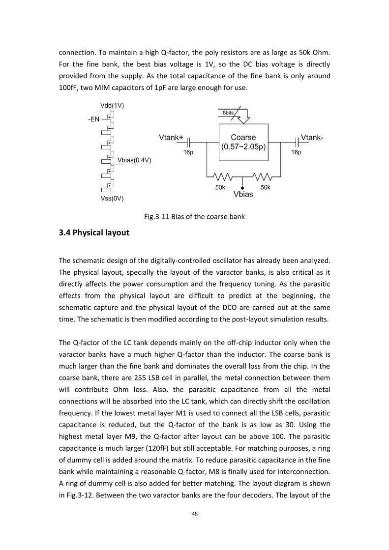
48
connection. To maintain a high Q-factor, the poly resistors are as large as 50k Ohm.
For the fine bank, the best bias voltage is 1V, so the DC bias voltage is directly
provided from the supply. As the total capacitance of the fine bank is only around
100fF, two MIM capacitors of 1pF are large enough for use.
Fig.3-11 Bias of the coarse bank
3.4 Physical layout
The schematic design of the digitally-controlled oscillator has already been analyzed.
The physical layout, specially the layout of the varactor banks, is also critical as it
directly affects the power consumption and the frequency tuning. As the parasitic
effects from the physical layout are difficult to predict at the beginning, the
schematic capture and the physical layout of the DCO are carried out at the same
time. The schematic is then modified according to the post-layout simulation results.
The Q-factor of the LC tank depends mainly on the off-chip inductor only when the
varactor banks have a much higher Q-factor than the inductor. The coarse bank is
much larger than the fine bank and dominates the overall loss from the chip. In the
coarse bank, there are 255 LSB cell in parallel, the metal connection between them
will contribute Ohm loss. Also, the parasitic capacitance from all the metal
connections will be absorbed into the LC tank, which can directly shift the oscillation
frequency. If the lowest metal layer M1 is used to connect all the LSB cells, parasitic
capacitance is reduced, but the Q-factor of the bank is as low as 30. Using the
highest metal layer M9, the Q-factor after layout can be above 100. The parasitic
capacitance is much larger (120fF) but still acceptable. For matching purposes, a ring
of dummy cell is added around the matrix. To reduce parasitic capacitance in the fine
bank while maintaining a reasonable Q-factor, M8 is finally used for interconnection.
A ring of dummy cell is also added for better matching. The layout diagram is shown
in Fig.3-12. Between the two varactor banks are the four decoders. The layout of the
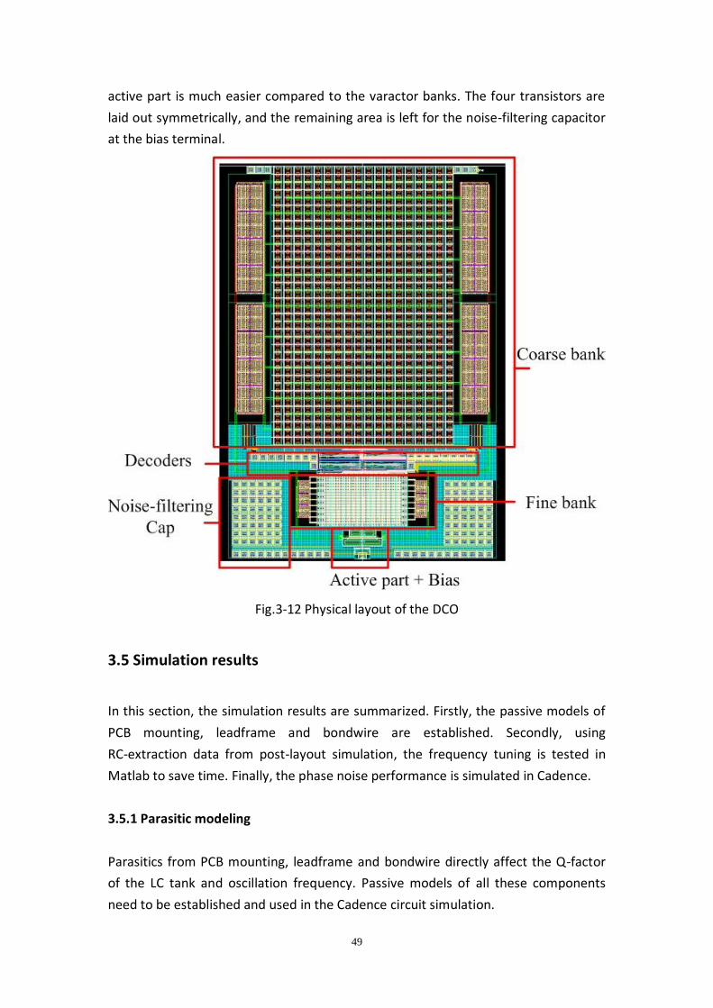
49
active part is much easier compared to the varactor banks. The four transistors are
laid out symmetrically, and the remaining area is left for the noise-filtering capacitor
at the bias terminal.
Fig.3-12 Physical layout of the DCO
3.5 Simulation results
In this section, the simulation results are summarized. Firstly, the passive models of
PCB mounting, leadframe and bondwire are established. Secondly, using
RC-extraction data from post-layout simulation, the frequency tuning is tested in
Matlab to save time. Finally, the phase noise performance is simulated in Cadence.
3.5.1 Parasitic modeling
Parasitics from PCB mounting, leadframe and bondwire directly affect the Q-factor
of the LC tank and oscillation frequency. Passive models of all these components
need to be established and used in the Cadence circuit simulation.
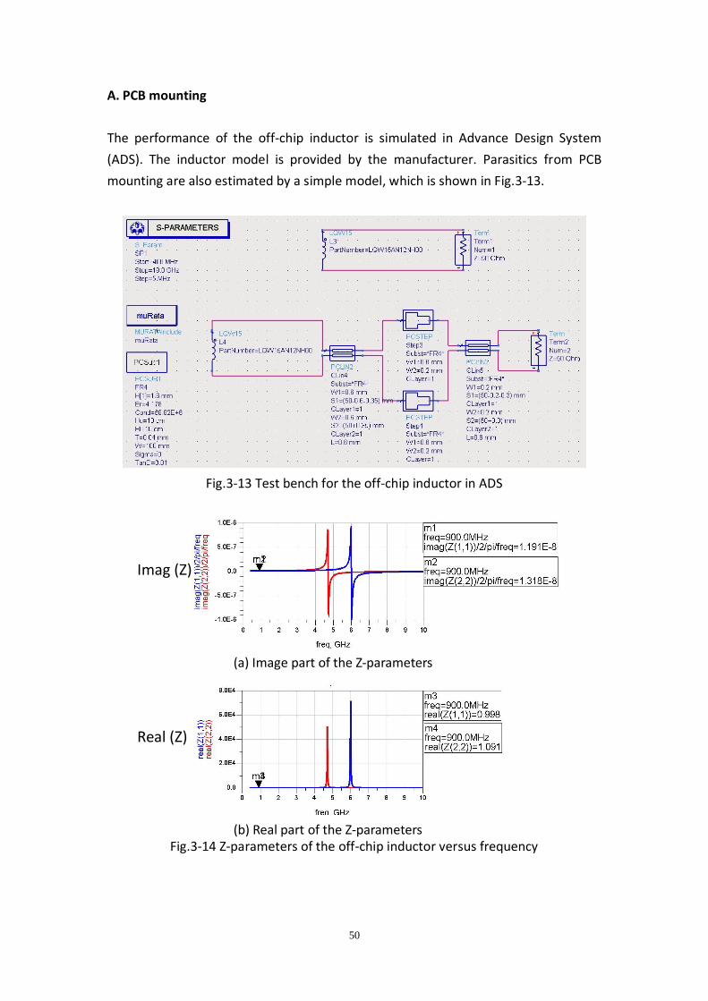
50
A. PCB mounting
The performance of the off-chip inductor is simulated in Advance Design System
(ADS). The inductor model is provided by the manufacturer. Parasitics from PCB
mounting are also estimated by a simple model, which is shown in Fig.3-13.
Fig.3-13 Test bench for the off-chip inductor in ADS
Fig.3-14 Z-parameters of the off-chip inductor versus frequency
Real (Z)
Imag (Z)
(a) Image part of the Z-parameters
(b) Real part of the Z-parameters
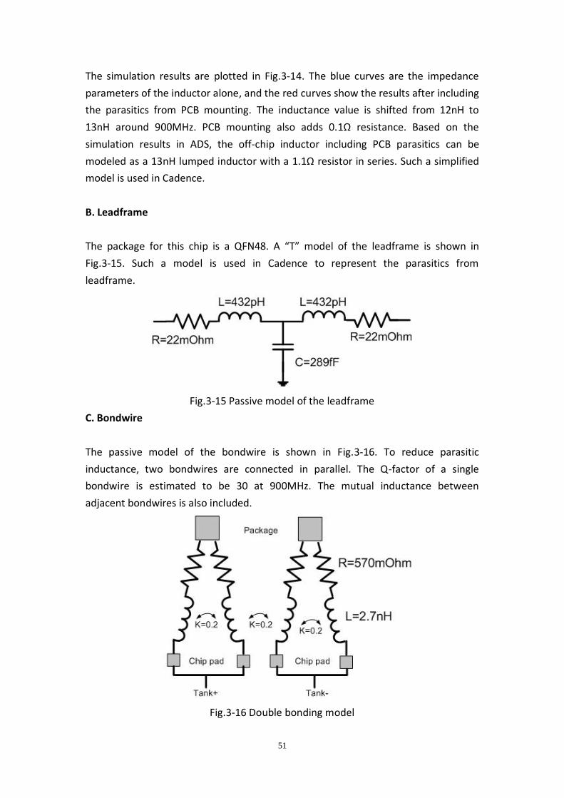
51
The simulation results are plotted in Fig.3-14. The blue curves are the impedance
parameters of the inductor alone, and the red curves show the results after including
the parasitics from PCB mounting. The inductance value is shifted from 12nH to
13nH around 900MHz. PCB mounting also adds 0.1Ω resistance. Based on the
simulation results in ADS, the off-chip inductor including PCB parasitics can be
modeled as a 13nH lumped inductor with a 1.1Ω resistor in series. Such a simplified
model is used in Cadence.
B. Leadframe
The package for this chip is a QFN48. A “T” model of the leadframe is shown in
Fig.3-15. Such a model is used in Cadence to represent the parasitics from
leadframe.
Fig.3-15 Passive model of the leadframe
C. Bondwire
The passive model of the bondwire is shown in Fig.3-16. To reduce parasitic
inductance, two bondwires are connected in parallel. The Q-factor of a single
bondwire is estimated to be 30 at 900MHz. The mutual inductance between
adjacent bondwires is also included.
Fig.3-16 Double bonding model

52
3.5.2 Frequency tuning
Table.3-2 Performance of the two varactor banks
Off On
C(F) Q C(F) Q
LSB cell in coarse bank (Schematic) 2.155f 675 7.953f 183
LSB cell in coarse bank (Layout) 2.646f 823 8.443f 192
Coarse bank (Schematic) 519.778f 268 1.622p 204
Coarse bank (Layout) 653.63f 241 1.731p 126
LSB cell in fine bank (Schematic) 77.9a >1000 253a >1000
LSB cell in fine bank (Layout) 275.5a >1000 451a >1000
Fine bank (Schematic) 19.16f 16 57.49f 56
Fine bank (Layout) 90.06f 98 119.26f 146
Table.3-2 summarizes the performance of the two varactor banks and the two kinds
of LSB cells. Based on post-layout RC-extraction and simulation, the coarse bank
produces about 120fF parasitic capacitance. When it is completely turned on, which
is the worst case, the Q-factor reduces to 126. For the fine bank, there is no precise
RF model of the NMOS transistor in schematic simulation, so the schematic and
post-layout simulation results show a large difference. After layout, the parasitic
capacitance is about 70fF and the Q-factor is around 100. Using the data from
post-layout simulation, the total tuning range and frequency resolution are tested in
Matlab. A simple equation-based model of the LC tank including the two varactor
banks is built and all the parasitics effects are included. The oscillation frequency
versus the total 16-bit tuning word is plotted in Fig.3-17. Each line segment (as
shown in the zoom-in figure) represents the tuning range of the fine bank when the
coarse tuning word is fixed at a certain value. The overlap of the two varactor banks
is proven. The coarse tuning range is from 764MHz to 1.024GHz, and the maximum

53
frequency step of the fine bank is 45kHz. All these parameters comply with the
design specifications.
Fig.3-17 Oscillation frequency versus 16-bit frequency tuning word
3.5.3 Phase noise and power consumption
As the two varactor banks are very complex, there are many internal signals. Due to
limited computer memory, phase noise is only simulated before layout. At the
lowest frequency point of 764MHz, the oscillation amplitude versus bias current and
phase noise versus oscillation amplitude are plotted in Fig.3-18. At the highest
frequency point 1.024GHz, these two curves are also plotted in Fig.3-19.
Fig.3-18 Output performances at the lowest frequency (764MHz)
Zoom-in

54
Fig.3-19 Output performances at the highest frequency (1.024GHz)
When the output amplitude is small, the transistors in the active part always work in
weak inversion region, so output amplitude is proportional to bias current. When the
amplitude is too large, the transistors are driven to cut off, so the amplitude tends to
clip. At the lowest frequency point, all the varactor cells are turned on, so the overall
Q-factor of the LC tank is lowest. To generate the same output amplitude, more bias
current is needed. At the highest frequency point, the bias current is smaller, so
output amplitude is saturated at a lower value. The phase noise performance can be
explained in [4]; the phase noise is inversely proportional to oscillation amplitude
until it goes into saturation. When the amplitude is too large, the active part will
generate more phase noise. The phase noise versus offset frequency at the best
situation is plotted in Fig.3-20.
Fig.3-20 Phase noise versus offset frequency
Offset frequency (Hz)
Phase noise (dBc/Hz)

55
A transient simulation is carried out after layout to test the functionality of this DCO.
As plotted in Fig.3-21, the DCO is firstly set to oscillate at the highest frequency.
After the raising edge of the clock signal, the two varactor tanks are turned on and
the DCO oscillates at the lowest frequency. Compared with schematic simulation
results, the oscillation amplitude is decreased by 50mV. This is mainly due to the
parasitic Ohm loss from the layout.
Fig.3-21 Transient simulation after layout
3.6 Conclusions
In this chapter, an ultra-low-power digitally-controlled oscillator is designed for
event-driven transmitter. Optimization of power consumption, frequency tuning and
phase noise are discussed in detail. Finally, the simulation results show that all the
design specifications are met as shown in Table.3-3.
Table.3-3 Simulated performance of the DCO
Center
frequency
Power
consumption
Phase noise
(@1MHz)
Tuning range Resolution
Design
specifications
900MHz <200uW <120dBc/Hz 810-990MHz <100kHz
Schematic
Simulations
900MHz <150uW <124dBc/Hz 764-1024MHz 45kHz
Voltage (V)
Time (uS)
Clock
Oscillation amplitude

56
References
[1] B. Razavi, “RF Microelectronics”, ISBN: 0138875715, Prentice Hall, Nov. 1997;
[2] Thomas H. Lee, “The Design of CMOS Radio-Frequency Integrated Circuits”, ISBN:
7121011271, Cambridge University Press, 2004;
[3] Ali Hajimiri and Thomas H. Lee, “Design Issues in CMOS Differential LC
Oscillators,” IEEE Journal of Solid-state Circuits, VOL.34, No.5, pp 717-724, May 1999;
[4] J.J. Rael and A. Abidi, “Physical processes of phase noise in differential LC
oscillators”, Proc. IEEE Custom Intergrated Circuits Conference, pp 569-572, 2000.

57
Chapter 4
Measurement results
In this chapter, the measurement results of the digitally-controlled oscillator (DCO)
designed in Chapter 3 will be presented. The physical layout of the complete
event-driven transmitter is first discussed, and then the measurement environment is
introduced. Power consumption, phase noise and frequency tuning of the DCO are
characterized. Preliminary results prove the correct functionality and reasonable
performance.
4.1 Chip gallery
Fig.4-1 Chip photo of the event-driven transmitter
The digitally-controlled oscillator is integrated into a complete event-driven
transmitter. The modulation type, operating frequency and power consumption of
the event-driven transmitter have already been analyzed in Chapter 2 and the circuit
diagram is shown in Fig.2-1. It is fabricated in TSMC’s 90nm CMOS technology.
Fig.4-1 shows the photomicrograph of the event-driven transmitter. Limited by the
number of pins, the 16-bit frequency tuning word of the DCO is controlled by a serial
peripheral interface (SPI). All the biases of the DCO and DCO buffer are also
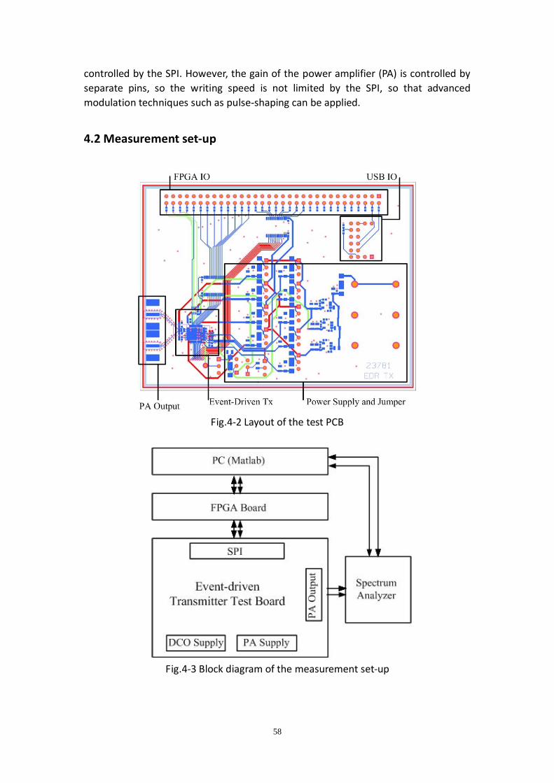
58
controlled by the SPI. However, the gain of the power amplifier (PA) is controlled by
separate pins, so the writing speed is not limited by the SPI, so that advanced
modulation techniques such as pulse-shaping can be applied.
4.2 Measurement set-up
Fig.4-2 Layout of the test PCB
Fig.4-3 Block diagram of the measurement set-up

59
The chip is placed in a QFN48 package, and then mounted on a test PCB. The PCB
layout is shown in Fig.4-2, and the measurement setup is outlined in Fig.4-3. A FPGA
board (Xilinx ML505) serves as an interface between the event-driven transmitter
and PC. All of the control signals, including the 16-bit frequency tuning word can be
written and read using Matlab. As the DCO does not have a separate output port, the
DCO performance is measured at the PA output using a spectrum analyzer (Agilent
E4440A). The PA and the DCO have separate power supplies. The power consumption
of the DCO can be measured by a DC current meter.
4.3 Measurement results
Frequency tuning, power consumption and phase noise and of the DCO are
measured under different bias conditions and frequencies. The results are
summarized in this section.
4.3.1 Frequency tuning
The frequency tuning range and resolution are both measured, and the tuning range
is verified. As shown in Fig.4-4, either turning on or off the fine bank, in these two
cases for each coarse tuning bit, the oscillation frequency are measured respectively.
Totally 512 frequency points are shown in Fig.4-4. The practical tuning range is from
855MHz to 1.104GHz, so the 902-928MHz ISM band is completely covered. The
matching of each LSB cell in the coarse bank is within ±10%. Increasing the coarse
tuning bit when the status of the fine bank is unchanged, the oscillation frequency
increases monotonically as expected. An overlap in frequency between the two
banks is also proven. The fine frequency tuning range can completely cover each
coarse tuning step. Even in the worst case, the same frequency can be covered by 4
times.
Fig.4-4 Frequency versus coarse tuning word
Zoom-in

60
The frequency resolution is measured in two cases. As shown in Fig.4-5, the coarse
bank is completely turned off so that the oscillation frequency is the lowest
(855MHz), and the oscillation frequency is measured at each fine tuning bit. Fig.4-6
shows the similar curve when the coarse bank is completely turned on so the
oscillation frequency is the highest (1.106GHz). As the total frequency change of the
fine bank is very small, these two frequency tuning curves are quite linear. The
frequency steps in these two cases are plotted in Fig.4-7. The measurement accuracy
is limited by the frequency resolution of the spectrum analyzer, but it can be
concluded that the matching of each LSB cell in the fine bank is within ±30%. The
average frequency resolution at the lowest frequency is 14kHz, while it is 30kHz at
the highest frequency.
Fig. 4-5 Frequency versus fine tuning word at the lowest frequency (855MHz)
Fig. 4-6 Frequency versus fine tuning word at the highest frequency (1.106GHz)
Zoom-in
Zoom-in

61
Fig.4-7 Frequency step versus fine tuning word
(Left: the lowest frequency. Right: the highest frequency.)
Table.4-1 Summary of frequency tuning
Center
frequency
Tuning range Resolution at
the lowest
frequency
Resolution at
the highest
frequency
Design specifications
900MHz 810-990MHz <100kHz <100kHz
Previous
Simulations
894MHz 764-1024MHz 19kHz 45kHz
Corrected
Simulations
968MHz 821-1115MHz 20kHz 48kHz
#1 test board
(12nH inductor)
980MHz 855-1106MHz 14kHz 30kHz
#2 test board
(15nH inductor)
895MHz 781-1009MHz 13kHz 27kHz
The measurement and simulation results are summarized in Table.4-1. Comparing
the measurement results of #1 test board with previous simulations, the main
difference lies in the center frequency. It shifts from 894MHz to 980MHz. This is likely
due to the inaccurate bondwire model during the design phase, which is proven as
follows.
A photograph of the packaged IC is shown in Fig.4-8, and the double-bonding for the
off-chip inductor is in the lower left corner. Practical physical parameters of the
bondwire are captured from Fig.4-8. The length of the bondwires is around 1540um.
The minimum distance between them is around 100um and the maximum distance is
around 350um. The parasitic effect of the bondwire is modeled again using Advanced
Design System (ADS). Self-inductance, coupling coefficient and Q-factor are simulated,

62
and the corrected values are compared with previous estimations in Table.4-2.
During the design phase, the self-inductance of the bondwires was estimated to be
2.7nH (1nH/mm) according to previous design projects. However, it can be concluded
that there is an error of 300% in the previous estimations. Based on the corrected
values, the frequency tuning performance is tested again in Cadence and Matlab. The
corrected simulation results are also shown in Table.4-1. After revising the bondwire
model, the simulation results are now close to the measurement results of #1 test
board.
According to the design specifications, the center frequency should be close to
900MH. A small modification is done to correct the frequency offset. The 12nH
off-chip inductor on #2 test board is replaced by a 15nH inductor, and then the
performance of #2 test board is measured using the same measurement set-up. The
results are also shown in Table.4-1. The center frequency goes back to 895MHz and
the other performance parameters are almost unchanged.
Fig.4-8 A photograph of the packaged IC
Table.4-2 Summary of bondwire models
Self-inductance Coupling
coefficient
(distance=100um)
Coupling
coefficient
(distance=200um)
Q(@1GHz)
Previous
estimations
2.7nH 0.2 0.1 30
Corrected
values
0.656nH 0.19 0.07 20

63
4.3.2 Power consumption and phase noise
Power consumption and phase noise are measured at 900MHz using #1 test board.
The curve of phase noise versus bias current is plotted in Fig.4-8. The phase noise is
measured at 1MHz offset frequency. The measurement results match the theoretical
estimation. As discussed in Chapter 3, increasing the bias current will increase the
oscillation amplitude. Phase noise is reduced until the amplitude is too large and the
transistors are cut-off periodically. Also, phase noise is measured in two situations. As
the two varactor banks are controlled by four binary-to-thermometer decoders, and
the clock signal of the decoders is inevitably coupled to the varactor banks by
parasitics, turning off the clock can improve the phase noise by 1 dBc. Under the best
bias condition when the clock is turned off, the curves of phase noise versus offset
frequency are plotted in Fig.4-9.
Fig.4-8 Phase noise versus bias current

64
Fig.4-9 Phase noise versus offset frequency
Fig.4-10 Phase noise versus bias current
(Left: lowest oscillation frequency. Right: highest oscillation frequency.)
To compare measurement with simulation results, phase noise is measured at the
lowest and highest oscillation frequencies and the simulation run again after revising
the bondwire model. The clock is turned off and the phase noise is measured and
simulated at 1MHz offset. The results are plotted in Fig.4-10. The best phase noise
result is 2dBc higher than the expected value in both cases. This can be explained by
three reasons. Firstly, the simulation is based on a schematic model, so all the
parasitics from layout are not included. Secondly, the power supply in the Cadence
simulation is ideal, but it inevitably produces noise in reality. Thirdly, the power

65
amplifier can also degrade the phase noise performance.
Other differences lie in the power consumption. The practical bias current is higher
than the simulation value to achieve the same phase noise level. As discussed above,
the simulation is based on schematic model and all the parasitics are not included.
Due to limited memory, the phase noise cannot be simulated after layout. However,
comparing the schematic simulation results, post-layout transient simulations show
that the differential output swing of the oscillator is decreased by 50mV. Also, the
swing is further decreased by 10mV when the input impedance of the oscillator
buffer is included during post-layout simulation. If the bias current is the same, the
practical output swing of the oscillator is smaller than the schematic simulation
result, so the phase noise is higher than the expected value.
Also, corner simulations were run to check the effect of variations in fabrication
process. As the active part and the coarse varactor bank dominate the power
consumption and phase noise performance, only these two blocks are tested. At the
highest oscillation frequency (bias current fixed at 50uA), different process corner
models are used. The results are summarized in Table.4-3. Due to the process
variations of the active part, the oscillation amplitude decreases 17mV and the phase
noise raises 4.8dB in the worst case. The process variations of the coarse bank mainly
affect the oscillation frequency. The maximum change in frequency is 12MHz. It is
therefore concluded that, the differences between simulation and measurement
results can also be explained partly by variations in fabrication process.
Table.4-3 Results of the corner simulations
Corner model Oscillation
frequency
Oscillation
amplitude
Phase noise
(@1MHz) NMOS
transistors
PMOS
transistors
MOS
varactors
Typical Typical Typical 1.115GHz 429mV -121.3dBc/Hz
Slow Slow Typical 1.118GHz 421mV -125.7dBc/Hz
Slow Fast Typical 1.116GHz 423mV -120.4dBc/Hz
Fast Slow Typical 1.116GHz 418mV -120.5dBc/Hz
Fast Fast Typical 1.112GHz 412mV -116.5dBc/Hz
Typical Typical Slow 1.127GHz 437mV -120.1dBc/Hz
Typical Typical Fast 1.103GHz 420mV -123.5dBc/Hz
In conclusion, there are many reasons to explain the differences between simulation
and measurement results. All of the parasitic effects from layout are not included in
the schematic simulation. Besides, process variations can also affect the performance.
Also, the practical Q-factor of the off-chip inductor may be lower than the expected
value. However, the degradation of power consumption and phase noise are still

66
acceptable. The power consumption is below 200uW and the phase noise is lower
than -120dBc/Hz at 1MHz offset in the worst case. The design specifications are
completely achieved.
4.4 Conclusions and comparisons
After introducing the measurement environment, the measurement results of the
digitally-controlled oscillator are summarized in this chapter. The correct functionality
and reasonable performance are proven. Wide frequency tuning and good frequency
resolution are shown, and monotonicity of the frequency tuning is verified. The
power consumption and phase noise are also close to the expected values and meet
the design specifications.
Table.4-4 compares this work with some state-of-the-art oscillators. Most of the
DCOs listed are not targeted for ultra-low-power applications. Although the tuning
range and frequency resolution are desirable, the power consumption is much larger
than 1mW except for the DCO in [1]. Appling a new architecture, the DCO in [4]
achieves the highest frequency resolution but at the cost of power consumption. On
the other hand, some VCOs and SAW-based oscillators are designed for
ultra-low-power applications but do not have the advantage of digital control. This
work implements an ultra-low-power digitally-controlled oscillator for event-driven
applications. The power consumption and phase noise performance are optimized,
while the frequency tuning range and resolution are comparable with state-of-the-art
DCOs.

67
Table.4-4 Summary of state-of-the-art oscillators
Inductor Frequency Power Tuning
range
Resolution Phase noise FOM
This
work
Off-chip 900MHz 180uW 228MHz
(25%)
30kHz -127dBc/Hz
@1MHz
-194
DCO[1] Bondwire 1.9GHz 100uW 155MHz
(8%)
200kHz -114dBc/Hz
@1MHz
-190
DCO[2] On-chip 2.4GHz 3.5mW 500MHz
(21%)
23kHz -112dBc/Hz
@500kHz
-180
DCO[3] On-chip 3.3GHz 2.4mW 600MHz
(18%)
5kHz -118dBc/Hz
@1MHz
-185
DCO[4] On-chip 3.3GHz 28.8mW 780MHz
(24%)
150Hz -128dBc/Hz
@1MHz
-183
VCO[5] On-chip 2.6GHz 430uW 200MHz
(8%)
- -106dBc/Hz
@400kHz
-186
VCO[6] Off-chip 900MHz 600uW 150MHz
(17%)
- -107dBc/Hz
@1MHz
-168
OCS[7] Off-chip 916.5MHz 800uW - - -114dBc/Hz
@1MHz
-174
OSC[8] SAW 433MHz 100uW - - -125dBc/Hz
@100kHz
-208
Figure of merit:
)1
log(10)log(20)/( 0
mW
P
f
ffLHzdBcFOM
.

68
References
[1] Pletcher and Rabaey, “A 100 uW, 1.9 GHz oscillator with fully digital frequency
tuning”, European Solid-State Circuits Conference, pp. 387–390, 2005.
[2] R. B. Staszewski, D. Leipold and P. T. Balsara, “A first multigigahertz digitally
controlled oscillator for wireless applications”, IEEE Transactions on Microwave
theory and techniques, vol. 51, pp. 2154 – 2164, Nov. 2005.
[3] J. Zhuang, Q. Du, T. Kwasniewski, “A 3.3 GHz LC-Base d Digitally Controlled
Oscillator with 5kHz Frequency Resolution”, Digest of Technical papers, IEEE Asian
Solid-State Circuits Conference, pp. 428 -131, 2007.
[4] Fanori, L., Liscidini, A., Castello, R., “Capacitive Degeneration in LC-Tank Oscillator
for DCO Fine-Frequency Tuning”, IEEE Journal of Solid-State Circuits, Volume: 45,
pp.2737-2745, Dec. 2010.
[5] Hanil Lee, Saeed Mohammadi, "A Subthreshold Low Phase Noise CMOS LC VCO
for Ultra Low Power Applications“, IEEE Microwave and Wireless Components Letters,
Vol. 17, No. 11, pp.796-798, November 2007.
[6] A. Molnar, B. Lu, S. Lanzisera, B.W. Cook, and K.S.J. Pister, “An Ultra-Low Power
900 MHz RF Transceiver for Wireless Sensor Networks”, Digest of Technical papers,
IEEE Custom Integrated Circuits Conference, pp. 401-404, 2004.
[7] D.C. Daly, Anantha P. Chandrakasan, "An Energy-Efficient OOK Transceiver for
Wireless Sensor Networks", IEEE Journal of Solid-State Circuits, Vol.42, No.5,
pp.1003-1011, May. 2007.
[8] M.K. Raja, Xu Yong Ping, "A 52 pJ/bit OOK transmitter with adaptable data rate“,
Aisa Solid-State Circuits Conference, pp.341-344, Nov. 2008.

69
Chapter 5
Conclusions
This work presents the design and testing of an ultra-low-power (ULP)
digitally-controlled oscillator (DCO), which is integrated into an event-driven
transmitter. It can be divided into three parts.
Firstly, the concept of event-driven communication is defined. Compared with
data-driven communication, event-driven communication is targeted for sharing
instant information of unexpected events. It relaxes the requirement of data rate but
places constraints on power consumption. Many applications can be classified into
event-driven communication such as active RF ID, industrial control and medical
monitoring.
Secondly, the design specifications and proposed circuit architecture of the
event-driven transmitter are discussed. The link budget is derived for both out-door
and in-door environments. The modulation type and operation frequency band are
also chosen carefully. After defining the design specifications, some state-of-the-art
designs are analyzed and then two potential solutions are provided. However,
SAW-based oscillator consumes unacceptable power under these design
specifications, so the DCO-based architecture is finally chosen.
Thirdly, the circuit design of this DCO is presented and the measurement results are
summarized. The oscillator is basically a LC oscillator, and the push-pull topology is
adopted for the active part. An off-chip inductor is used to reduce the loss in the LC
tank. Wide frequency tuning range and high resolution are achieved by
implementing two varactor banks. Creative control logic is carried out to guarantee
the monotonicity of frequency tuning. Phase noise performance is also optimized
during the design phase. The chip is designed in TSMC ’s 90nm CMOS technology.
Measurement results prove the correct functionality and reasonable performance.
Based on the design and measurement results, two main tasks are left for future
research. Firstly, further measurements should be carried out to test the
performance of the complete event-driven transmitter, including the DCO buffer and
power amplifier. Also, this transmitter should be tested together with the
event-driven receiver to demonstrate two-way communication. Secondly, the
frequency calibration loop should be implemented on a FPGA and then integrated
with the RF front-end. The frequency divider is already implemented and connected
to the FPGA board. A simple frequency-locked loop can be designed to automatically
control the oscillation frequency of the DCO. If so, the event-driven transmitter
prototype is complete.
Related Documents