electronics Review Ultra-Low-Power Design and Hardware Security Using Emerging Technologies for Internet of Things Jiann-Shiun Yuan *, Jie Lin, Qutaiba Alasad and Shayan Taheri ID Department of Electrical and Computer Engineering, University of Central Florida, Orlando, FL 32816, USA; [email protected] (J.L.); [email protected] (Q.A.); [email protected] (S.T.) * Correspondence: [email protected]; Tel.: +2-1-407-823-5719 Received: 1 August 2017; Accepted: 5 September 2017; Published: 8 September 2017 Abstract: In this review article for Internet of Things (IoT) applications, important low-power design techniques for digital and mixed-signal analog–digital converter (ADC) circuits are presented. Emerging low voltage logic devices and non-volatile memories (NVMs) beyond CMOS are illustrated. In addition, energy-constrained hardware security issues are reviewed. Specifically, light-weight encryption-based correlational power analysis, successive approximation register (SAR) ADC security using tunnel field effect transistors (FETs), logic obfuscation using silicon nanowire FETs, and all-spin logic devices are highlighted. Furthermore, a novel ultra-low power design using bio-inspired neuromorphic computing and spiking neural network security are discussed. Keywords: ADC; DPA; emerging technologies; hardware security; neuromorphic computing; side-channel attack; Trojans; tunnel FET; ultra-low power 1. Introduction Advances in wired and wireless sensor networks have laid a solid foundation for the Internet of Things (IoT). It is estimated that around 30 billion IoT devices will be connected to the Internet by 2020 [1]. Examples of these devices include sensors, RFID tags, smart thermostats, and smart phones and gadgets. Those devices will be empowered to sense, process, and control the physical world events. Eventually, the IoT will lead us to the Internet of Everything (IoE), where the virtual world of information is integrated with the physical world of objects. The Internet of Things incorporates devices from a very diverse background. These devices differ from each other in terms of their size, storage, energy consumption, computation, data rate, and other performance metrics. Seamless and interoperable communication among them is enabled via sensors and actuators embedded in them. These miniature sensors give a unique ID to each participating device in an IoT paradigm. Sensors broaden the scope and scalability of today’s Internet by integrating them to the physical systems. However, it requires effort from the application developer’s side because sensors are tiny, energy-starved, and constrained on computation and storage capacity. Designing secure solutions in the IoT system is difficult and complex due to the peculiar nature of the devices. Since sensors are computing-power-constrained and deployable from anywhere in the world, they are vulnerable to cyber attacks and have thus become the weakest link in the IoT system. In this review paper, energy-constrained IoT devices for low-power design and security assurance are presented. Section 2 discusses key low-power design techniques for today’s chip applications. Section 3 illustrates emerging technologies in logic and memory devices beyond CMOS (more than Moore). Steep sub-threshold slope transistors as well as resistive, phase change, and spin transfer torque (STT) memories are explained. Section 4 combines the near-threshold low-power technique using emerging tunnel FET (TFET) technology for logic gates and successive approximation register (SAR) analog-to-digital converter (ADC) designs. In addition, the noise shaping (NS) technique is Electronics 2017, 6, 67; doi:10.3390/electronics6030067 www.mdpi.com/journal/electronics

Welcome message from author
This document is posted to help you gain knowledge. Please leave a comment to let me know what you think about it! Share it to your friends and learn new things together.
Transcript
electronics
Review
Ultra-Low-Power Design and Hardware SecurityUsing Emerging Technologies for Internet of Things
Jiann-Shiun Yuan *, Jie Lin, Qutaiba Alasad and Shayan Taheri ID
Department of Electrical and Computer Engineering, University of Central Florida, Orlando, FL 32816, USA;[email protected] (J.L.); [email protected] (Q.A.); [email protected] (S.T.)* Correspondence: [email protected]; Tel.: +2-1-407-823-5719
Received: 1 August 2017; Accepted: 5 September 2017; Published: 8 September 2017
Abstract: In this review article for Internet of Things (IoT) applications, important low-powerdesign techniques for digital and mixed-signal analog–digital converter (ADC) circuits are presented.Emerging low voltage logic devices and non-volatile memories (NVMs) beyond CMOS are illustrated.In addition, energy-constrained hardware security issues are reviewed. Specifically, light-weightencryption-based correlational power analysis, successive approximation register (SAR) ADC securityusing tunnel field effect transistors (FETs), logic obfuscation using silicon nanowire FETs, and all-spinlogic devices are highlighted. Furthermore, a novel ultra-low power design using bio-inspiredneuromorphic computing and spiking neural network security are discussed.
Keywords: ADC; DPA; emerging technologies; hardware security; neuromorphic computing;side-channel attack; Trojans; tunnel FET; ultra-low power
1. Introduction
Advances in wired and wireless sensor networks have laid a solid foundation for the Internetof Things (IoT). It is estimated that around 30 billion IoT devices will be connected to the Internet by2020 [1]. Examples of these devices include sensors, RFID tags, smart thermostats, and smart phonesand gadgets. Those devices will be empowered to sense, process, and control the physical worldevents. Eventually, the IoT will lead us to the Internet of Everything (IoE), where the virtual world ofinformation is integrated with the physical world of objects.
The Internet of Things incorporates devices from a very diverse background. These devices differfrom each other in terms of their size, storage, energy consumption, computation, data rate, and otherperformance metrics. Seamless and interoperable communication among them is enabled via sensorsand actuators embedded in them. These miniature sensors give a unique ID to each participatingdevice in an IoT paradigm. Sensors broaden the scope and scalability of today’s Internet by integratingthem to the physical systems. However, it requires effort from the application developer’s sidebecause sensors are tiny, energy-starved, and constrained on computation and storage capacity.Designing secure solutions in the IoT system is difficult and complex due to the peculiar natureof the devices. Since sensors are computing-power-constrained and deployable from anywhere in theworld, they are vulnerable to cyber attacks and have thus become the weakest link in the IoT system.
In this review paper, energy-constrained IoT devices for low-power design and security assuranceare presented. Section 2 discusses key low-power design techniques for today’s chip applications.Section 3 illustrates emerging technologies in logic and memory devices beyond CMOS (more thanMoore). Steep sub-threshold slope transistors as well as resistive, phase change, and spin transfertorque (STT) memories are explained. Section 4 combines the near-threshold low-power techniqueusing emerging tunnel FET (TFET) technology for logic gates and successive approximation register(SAR) analog-to-digital converter (ADC) designs. In addition, the noise shaping (NS) technique is
Electronics 2017, 6, 67; doi:10.3390/electronics6030067 www.mdpi.com/journal/electronics
Electronics 2017, 6, 67 2 of 55
adopted to increase the effective number of bits for the SAR ADC. Bio-inspired ultra-low-powerneuromorphic computing for unsupervised learning and recognition is introduced in this sectionas well. Various hardware security issues are highlighted in Section 5. These include importantencryption techniques, side channel attack/defense, logic locking/split manufacturing againstreverse-engineering/counterfeiting, and camouflage layout. The uses of emerging technologies andlightweight encryption for correlation power analysis against side channel attack, silicon nanowirepolymorphic gates, and all-spin logic devices for deception and logic locking, and a TFET secure SARADC design for Trojan countermeasures are shown in Section 6. Finally, a summary of this work isgiven in Section 7.
2. Key Low Power Techniques in Digital, Analog, and Mixed-Signal Circuits
2.1. Digital Circuits
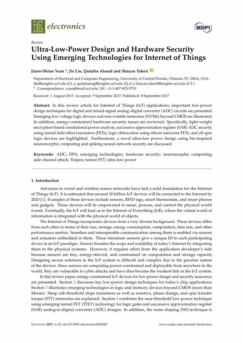
Scaling of CMOS devices have continued for many decades to provide faster switching speedand lower power consumption. Numerous enabling approaches such as high-κ/metal gate [2,3] andFinFET [4,5] have been used. Since the dynamic power dissipation of CMOS logic is proportionalto the square of supply voltage VDD, VDD scaling provides a way to constrain power dissipation ofintegrated circuits (ICs). However, when CMOS logic is operating at the sub-threshold voltage level,a significant increase in leakage power and circuit delay occurs [6]. Near threshold operation offers theoptimization of power and performance tradeoff (see Figure 1). In addition, three-dimensional (3D)integration of IC using through silicon vias (TSVs) can enhance chip performance [7].
Electronics 2017, 6, 67 2 of 54
shaping (NS) technique is adopted to increase the effective number of bits for the SAR ADC. Bio‐
inspired ultra‐low‐power neuromorphic computing for unsupervised learning and recognition is
introduced in this section as well. Various hardware security issues are highlighted in Section 5. These
include important encryption techniques, side channel attack/defense, logic locking/split
manufacturing against reverse‐engineering/counterfeiting, and camouflage layout. The uses of
emerging technologies and lightweight encryption for correlation power analysis against side
channel attack, silicon nanowire polymorphic gates, and all‐spin logic devices for deception and logic
locking, and a TFET secure SAR ADC design for Trojan countermeasures are shown in Section 6.
Finally, a summary of this work is given in Section 7.
2. Key Low Power Techniques in Digital, Analog, and Mixed‐Signal Circuits
2.1. Digital Circuits
Scaling of CMOS devices have continued for many decades to provide faster switching speed
and lower power consumption. Numerous enabling approaches such as high‐κ/metal gate [2,3] and
FinFET [4,5] have been used. Since the dynamic power dissipation of CMOS logic is proportional to
the square of supply voltage VDD, VDD scaling provides a way to constrain power dissipation of
integrated circuits (ICs). However, when CMOS logic is operating at the sub‐threshold voltage level,
a significant increase in leakage power and circuit delay occurs [6]. Near threshold operation offers
the optimization of power and performance tradeoff (see Figure 1). In addition, three‐dimensional
(3D) integration of IC using through silicon vias (TSVs) can enhance chip performance [7].
Supply Voltage
Log
(Dela
y)
Large EnergyIncrease
Balanced Trade-Offs
Large DelayIncrease
Vth
~50-100X
~10X
~10X
Vnormal
Super-Vth
Region
Near-Vth
Region
Ene
rgy/
Ope
ratio
n Sub-Vth
Region
~2X
Figure 1. Energy and delay plots versus supply voltage scaling.
Energy efficiency is a major issue in modern digital systems. High computation demand has led
academia and industry to provide architectural approaches for multicore and many‐core systems that
exploit system‐wide power efficiency for a particular application domain. Power saving methods
such as dynamic voltage and frequency scaling (DVFS) [8] is widely used in applications. DVFS scales
the supply voltage and clock frequency based on the work load at run time. In DVFS, the power
dissipation is controlled by adjusting the processor’s voltage and frequency. Voltage and frequency
scaling to offer power reduction has been implemented in commercial chips [9].
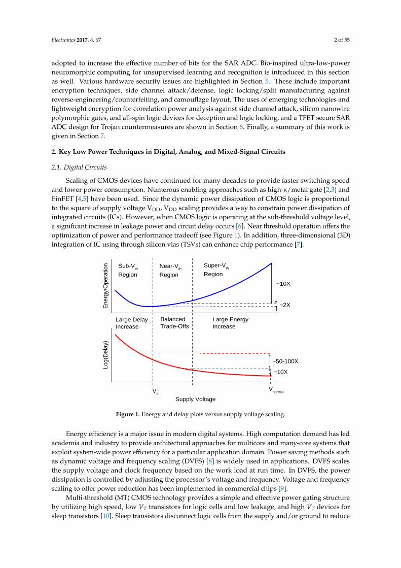
Multi‐threshold (MT) CMOS technology provides a simple and effective power gating structure
by utilizing high speed, low VT transistors for logic cells and low leakage, and high VT devices for
sleep transistors [10]. Sleep transistors disconnect logic cells from the supply and/or ground to reduce
the leakage in standby mode (see Figure 2). More precisely, multi‐threshold CMOS uses low‐leakage
NMOS (PMOS) transistors as footer (header) switches to disconnect ground (power supply) from
parts of a design in the circuit standby mode. There is a large amount of rush‐through current from
Figure 1. Energy and delay plots versus supply voltage scaling.
Energy efficiency is a major issue in modern digital systems. High computation demand has ledacademia and industry to provide architectural approaches for multicore and many-core systems thatexploit system-wide power efficiency for a particular application domain. Power saving methods suchas dynamic voltage and frequency scaling (DVFS) [8] is widely used in applications. DVFS scalesthe supply voltage and clock frequency based on the work load at run time. In DVFS, the powerdissipation is controlled by adjusting the processor’s voltage and frequency. Voltage and frequencyscaling to offer power reduction has been implemented in commercial chips [9].
Multi-threshold (MT) CMOS technology provides a simple and effective power gating structureby utilizing high speed, low VT transistors for logic cells and low leakage, and high VT devices forsleep transistors [10]. Sleep transistors disconnect logic cells from the supply and/or ground to reduce
Electronics 2017, 6, 67 3 of 55
the leakage in standby mode (see Figure 2). More precisely, multi-threshold CMOS uses low-leakageNMOS (PMOS) transistors as footer (header) switches to disconnect ground (power supply) from partsof a design in the circuit standby mode. There is a large amount of rush-through current from thepower supply to ground when a multi-threshold CMOS circuit switches from sleep to active mode.On the other hand, when an MT CMOS circuit switches from sleep to active mode, it takes some time(wakeup latency) for the circuit to become functional and start working at its full performance level.Without some kind of always-on latches, the internal state of the MTCMOS circuit is lost when it isput into sleep mode. Because of the large amount of rush-through current and large wakeup latencyfor MTCMOS circuits, for short standby periods, it is better to put the circuit into an intermediatepower-saving mode (called the drowsy mode). The reason is that the transition latency from thedrowsy to active mode is much less than the wakeup time of the circuit when coming out of the sleepmode. Furthermore, if designed appropriately, drowsy circuits can retain a pre-standby internal stateof the circuit. The downside of putting a circuit into drowsy mode is the higher amount of the leakagecurrent compared to the case when the circuit is put into sleep mode.
Electronics 2017, 6, 67 3 of 54
the power supply to ground when a multi‐threshold CMOS circuit switches from sleep to active
mode. On the other hand, when an MT CMOS circuit switches from sleep to active mode, it takes
some time (wakeup latency) for the circuit to become functional and start working at its full
performance level. Without some kind of always‐on latches, the internal state of the MTCMOS circuit
is lost when it is put into sleep mode. Because of the large amount of rush‐through current and large
wakeup latency for MTCMOS circuits, for short standby periods, it is better to put the circuit into an
intermediate power‐saving mode (called the drowsy mode). The reason is that the transition latency
from the drowsy to active mode is much less than the wakeup time of the circuit when coming out
of the sleep mode. Furthermore, if designed appropriately, drowsy circuits can retain a pre‐standby
internal state of the circuit. The downside of putting a circuit into drowsy mode is the higher amount
of the leakage current compared to the case when the circuit is put into sleep mode.
Circuit Block
MS1
MS2
MD2
MD1
MS
SLEEP
Sleep Inverter
VDD
VVSS
GS
DROWSY
Figure 2. Implementation of sleep mode design.
In recent years, multi‐core systems have become standard in the computer industry. The design
of multi‐cores takes advantage of thread‐level parallelism in applications that are computationally
intensive and highly parallel. Energy efficiency is one of the biggest challenges in the design of multi‐
core systems, and workload imbalance among parallel threads is one of the sources of energy
inefficiency. DVFS thus can save energy consumption on multi‐cores, but all of them assume that
each core in a multi‐core system contains only one hardware context and only one thread can execute
on one core at a time. However, mainstream multi‐core systems are moving to have simultaneous
multi‐threading (SMT) support in cores, and existing DVFS‐based techniques are not effective to
achieve maximum energy savings. A novel technique called thread shuffling, which combines thread
migration and DVFS to achieve maximum energy savings and maintain performance on a multi‐core
system supporting SMT was proposed [11]. Thread shuffling is implemented and simulated in a
cycle‐accurate ×86 multi‐core system. The experiments show that it achieves up to 56% energy
savings without performance penalty for selected Recognition, Mining, and Synthesis (RMS)
applications from Intel Labs.
Other low‐power design techniques include clocking gating [12], pipeline architecture [13],
asynchronous signal transmission [14], and software and hardware co‐design [15]. Asynchronous
circuit design has long been a designer’s interest. The advantages of asynchronous circuits include
lower peak power dissipation, lower electromagnetic emission (EMI), free interchangeability of
components between systems, and are more robust against temperature and process variations [16].
Asynchronous circuits, especially quasi‐delay‐insensitive asynchronous circuits, use local
handshaking protocols in lieu of clocks to coordinate circuit behavior. The delay insensitivity and
other unique features of quasi‐delay‐insensitive circuits allow for a more aggressive supply voltage
scaling, implementing power gating without timing analysis or extra control overhead [17].
Figure 2. Implementation of sleep mode design.
In recent years, multi-core systems have become standard in the computer industry. The designof multi-cores takes advantage of thread-level parallelism in applications that are computationallyintensive and highly parallel. Energy efficiency is one of the biggest challenges in the design ofmulti-core systems, and workload imbalance among parallel threads is one of the sources of energyinefficiency. DVFS thus can save energy consumption on multi-cores, but all of them assume thateach core in a multi-core system contains only one hardware context and only one thread can executeon one core at a time. However, mainstream multi-core systems are moving to have simultaneousmulti-threading (SMT) support in cores, and existing DVFS-based techniques are not effective toachieve maximum energy savings. A novel technique called thread shuffling, which combinesthread migration and DVFS to achieve maximum energy savings and maintain performance ona multi-core system supporting SMT was proposed [11]. Thread shuffling is implemented andsimulated in a cycle-accurate ×86 multi-core system. The experiments show that it achieves upto 56% energy savings without performance penalty for selected Recognition, Mining, and Synthesis(RMS) applications from Intel Labs.
Other low-power design techniques include clocking gating [12], pipeline architecture [13],asynchronous signal transmission [14], and software and hardware co-design [15]. Asynchronous
Electronics 2017, 6, 67 4 of 55
circuit design has long been a designer’s interest. The advantages of asynchronous circuits includelower peak power dissipation, lower electromagnetic emission (EMI), free interchangeability ofcomponents between systems, and are more robust against temperature and process variations [16].Asynchronous circuits, especially quasi-delay-insensitive asynchronous circuits, use local handshakingprotocols in lieu of clocks to coordinate circuit behavior. The delay insensitivity and other uniquefeatures of quasi-delay-insensitive circuits allow for a more aggressive supply voltage scaling,implementing power gating without timing analysis or extra control overhead [17]. Asynchronouscircuits connect multiple components effectively across a large die for energy efficiency.
Comparing various low-power design trade-offs or additional requirements, multi-thresholdvoltage technique requires the support of semiconductor process to make MOSFETs available withdifferent threshold voltages. Asynchronous circuits may consume more chip area due to additionalhandshaking circuit components and dual rail encoding. Multi-core design requires parallel clocktrees and needs additional interconnections on silicon among different cores. DVFS requires on-chipDC-DC converter for supply voltage scaling.
In addition to low-power mobile computing, energy saving in wireless communication isimportant for IoT applications. Clearly, energy efficient mobile computing requires an ultra-low-powersystem design [18]. Achieving a very low average power for a wireless system typically makesextensive use of duty cycling. The aim is to reduce the device “on” time to a short communication burst,and then between these active periods have the device enter a sleep mode to save power consumption.
2.2. Analog Circuits
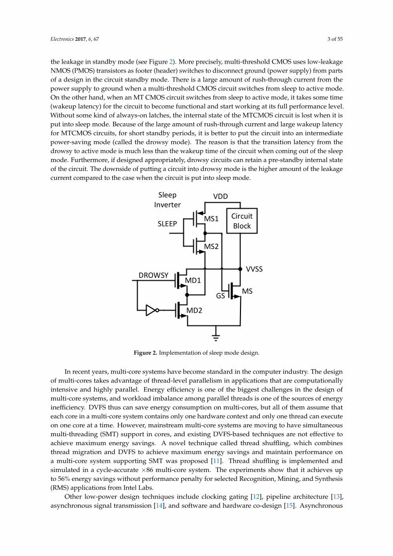
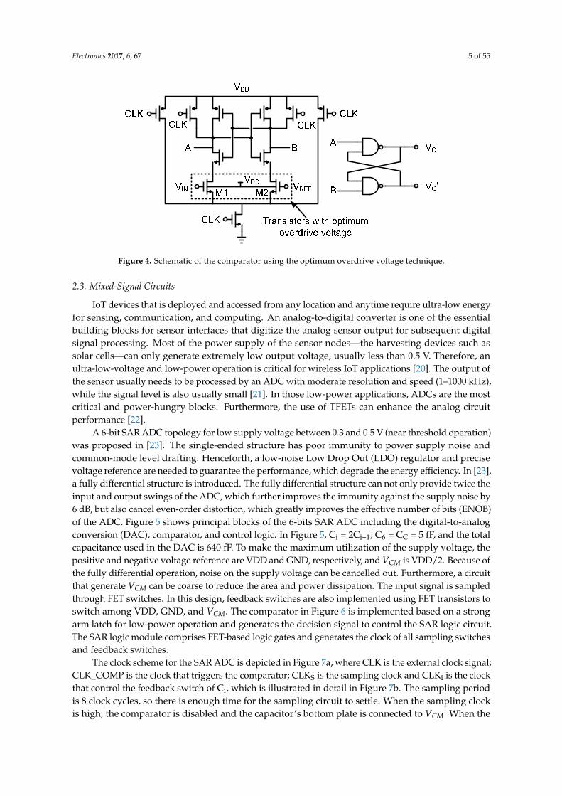
Low-voltage operation in the analog circuit could be quite different from that of the digital circuit.For example, when the supply voltage is reduced to the near-threshold voltage of the MOSFET, theoverdrive voltage (OV) or the voltage headroom is limited, which introduces a significant temperatureshift of cutoff frequency of the MOS transistor and hence hinders the performance of the analog circuit.To address this temperature drift issue, Lin and Yuan [19] used an optimum overdrive voltage to reducetemperature sensitivity. With the mutual temperature compensation of carrier mobility and thresholdvoltage, the optimal bias point makes the cutoff frequency insensitive to temperature variation, asshown in Figure 3. A comparator using the optimum overdrive voltage technique is shown in Figure 4.
Electronics 2017, 6, 67 4 of 54
Asynchronous circuits connect multiple components effectively across a large die for energy
efficiency.
Comparing various low‐power design trade‐offs or additional requirements, multi‐threshold
voltage technique requires the support of semiconductor process to make MOSFETs available with
different threshold voltages. Asynchronous circuits may consume more chip area due to additional
handshaking circuit components and dual rail encoding. Multi‐core design requires parallel clock
trees and needs additional interconnections on silicon among different cores. DVFS requires on‐chip
DC‐DC converter for supply voltage scaling.
In addition to low‐power mobile computing, energy saving in wireless communication is
important for IoT applications. Clearly, energy efficient mobile computing requires an ultra‐low‐
power system design [18]. Achieving a very low average power for a wireless system typically makes
extensive use of duty cycling. The aim is to reduce the device “on” time to a short communication
burst, and then between these active periods have the device enter a sleep mode to save power
consumption.
2.2. Analog Circuits
Low‐voltage operation in the analog circuit could be quite different from that of the digital
circuit. For example, when the supply voltage is reduced to the near‐threshold voltage of the
MOSFET, the overdrive voltage (OV) or the voltage headroom is limited, which introduces a
significant temperature shift of cutoff frequency of the MOS transistor and hence hinders the
performance of the analog circuit. To address this temperature drift issue, Lin and Yuan [19] used an
optimum overdrive voltage to reduce temperature sensitivity. With the mutual temperature
compensation of carrier mobility and threshold voltage, the optimal bias point makes the cutoff
frequency insensitive to temperature variation, as shown in Figure 3. A comparator using the
optimum overdrive voltage technique is shown in Figure 4.
-60 -40 -20 0 20 40 60 80 100 120 140
0
1x10⁹
2x10⁹
3x10⁹
4x10⁹
5x10⁹
6x10⁹
fT of the MOSFET with OV
fT of the MOSFET without OV
f T (
Hz)
Temperature oC
Figure 3. Cutoff frequency versus temperature. Figure 3. Cutoff frequency versus temperature.
Electronics 2017, 6, 67 5 of 55Electronics 2017, 6, 67 5 of 54
Figure 4. Schematic of the comparator using the optimum overdrive voltage technique.
2.3. Mixed‐Signal Circuits
IoT devices that is deployed and accessed from any location and anytime require ultra‐low
energy for sensing, communication, and computing. An analog‐to‐digital converter is one of the
essential building blocks for sensor interfaces that digitize the analog sensor output for subsequent
digital signal processing. Most of the power supply of the sensor nodes—the harvesting devices such
as solar cells—can only generate extremely low output voltage, usually less than 0.5 V. Therefore, an
ultra‐low‐voltage and low‐power operation is critical for wireless IoT applications [20]. The output
of the sensor usually needs to be processed by an ADC with moderate resolution and speed (1–1000
kHz), while the signal level is also usually small [21]. In those low‐power applications, ADCs are the
most critical and power‐hungry blocks. Furthermore, the use of TFETs can enhance the analog circuit
performance [22].
A 6‐bit SAR ADC topology for low supply voltage between 0.3 and 0.5 V (near threshold
operation) was proposed in [23]. The single‐ended structure has poor immunity to power supply
noise and common‐mode level drafting. Henceforth, a low‐noise Low Drop Out (LDO) regulator and
precise voltage reference are needed to guarantee the performance, which degrade the energy
efficiency. In [23], a fully differential structure is introduced. The fully differential structure can not
only provide twice the input and output swings of the ADC, which further improves the immunity
against the supply noise by 6 dB, but also cancel even‐order distortion, which greatly improves the
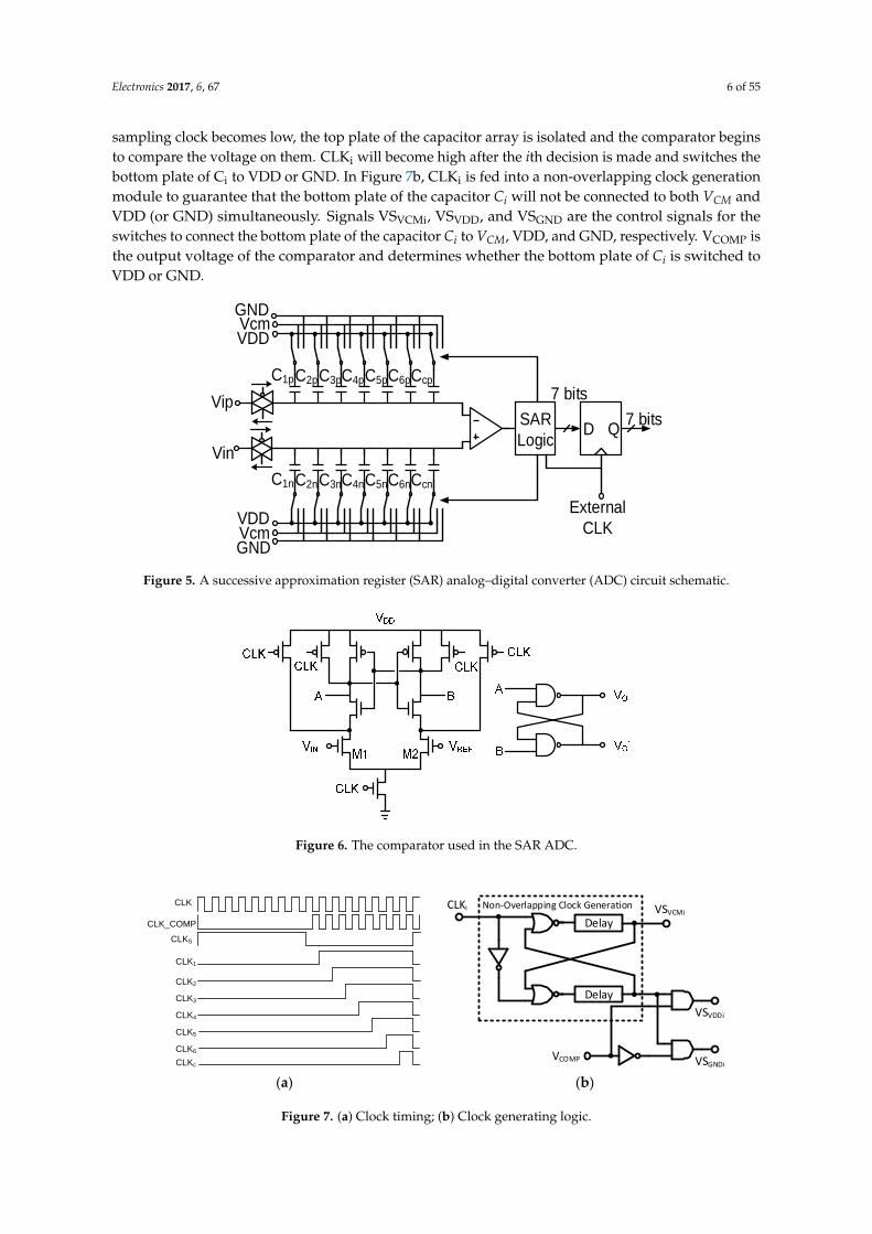
effective number of bits (ENOB) of the ADC. Figure 5 shows principal blocks of the 6‐bits SAR ADC
including the digital‐to‐analog conversion (DAC), comparator, and control logic. In Figure 5, Ci =
2Ci+1; C6 = CC = 5 fF, and the total capacitance used in the DAC is 640 fF. To make the maximum
utilization of the supply voltage, the positive and negative voltage reference are VDD and GND,
respectively, and VCM is VDD/2. Because of the fully differential operation, noise on the supply
voltage can be cancelled out. Furthermore, a circuit that generate VCM can be coarse to reduce the area
and power dissipation. The input signal is sampled through FET switches. In this design, feedback
switches are also implemented using FET transistors to switch among VDD, GND, and VCM. The
comparator in Figure 6 is implemented based on a strong arm latch for low‐power operation and
generates the decision signal to control the SAR logic circuit. The SAR logic module comprises FET‐
based logic gates and generates the clock of all sampling switches and feedback switches.
The clock scheme for the SAR ADC is depicted in Figure 7a, where CLK is the external clock
signal; CLK_COMP is the clock that triggers the comparator; CLKS is the sampling clock and CLKi is
the clock that control the feedback switch of Ci, which is illustrated in detail in Figure 7b. The
sampling period is 8 clock cycles, so there is enough time for the sampling circuit to settle. When the
sampling clock is high, the comparator is disabled and the capacitor’s bottom plate is connected to
VCM. When the sampling clock becomes low, the top plate of the capacitor array is isolated and the
comparator begins to compare the voltage on them. CLKi will become high after the ith decision is
made and switches the bottom plate of Ci to VDD or GND. In Figure 7b, CLKi is fed into a non‐
Figure 4. Schematic of the comparator using the optimum overdrive voltage technique.
2.3. Mixed-Signal Circuits
IoT devices that is deployed and accessed from any location and anytime require ultra-low energyfor sensing, communication, and computing. An analog-to-digital converter is one of the essentialbuilding blocks for sensor interfaces that digitize the analog sensor output for subsequent digitalsignal processing. Most of the power supply of the sensor nodes—the harvesting devices such assolar cells—can only generate extremely low output voltage, usually less than 0.5 V. Therefore, anultra-low-voltage and low-power operation is critical for wireless IoT applications [20]. The output ofthe sensor usually needs to be processed by an ADC with moderate resolution and speed (1–1000 kHz),while the signal level is also usually small [21]. In those low-power applications, ADCs are the mostcritical and power-hungry blocks. Furthermore, the use of TFETs can enhance the analog circuitperformance [22].
A 6-bit SAR ADC topology for low supply voltage between 0.3 and 0.5 V (near threshold operation)was proposed in [23]. The single-ended structure has poor immunity to power supply noise andcommon-mode level drafting. Henceforth, a low-noise Low Drop Out (LDO) regulator and precisevoltage reference are needed to guarantee the performance, which degrade the energy efficiency. In [23],a fully differential structure is introduced. The fully differential structure can not only provide twice theinput and output swings of the ADC, which further improves the immunity against the supply noise by6 dB, but also cancel even-order distortion, which greatly improves the effective number of bits (ENOB)of the ADC. Figure 5 shows principal blocks of the 6-bits SAR ADC including the digital-to-analogconversion (DAC), comparator, and control logic. In Figure 5, Ci = 2Ci+1; C6 = CC = 5 fF, and the totalcapacitance used in the DAC is 640 fF. To make the maximum utilization of the supply voltage, thepositive and negative voltage reference are VDD and GND, respectively, and VCM is VDD/2. Because ofthe fully differential operation, noise on the supply voltage can be cancelled out. Furthermore, a circuitthat generate VCM can be coarse to reduce the area and power dissipation. The input signal is sampledthrough FET switches. In this design, feedback switches are also implemented using FET transistors toswitch among VDD, GND, and VCM. The comparator in Figure 6 is implemented based on a strongarm latch for low-power operation and generates the decision signal to control the SAR logic circuit.The SAR logic module comprises FET-based logic gates and generates the clock of all sampling switchesand feedback switches.
The clock scheme for the SAR ADC is depicted in Figure 7a, where CLK is the external clock signal;CLK_COMP is the clock that triggers the comparator; CLKS is the sampling clock and CLKi is the clockthat control the feedback switch of Ci, which is illustrated in detail in Figure 7b. The sampling periodis 8 clock cycles, so there is enough time for the sampling circuit to settle. When the sampling clockis high, the comparator is disabled and the capacitor’s bottom plate is connected to VCM. When the
Electronics 2017, 6, 67 6 of 55
sampling clock becomes low, the top plate of the capacitor array is isolated and the comparator beginsto compare the voltage on them. CLKi will become high after the ith decision is made and switches thebottom plate of Ci to VDD or GND. In Figure 7b, CLKi is fed into a non-overlapping clock generationmodule to guarantee that the bottom plate of the capacitor Ci will not be connected to both VCM andVDD (or GND) simultaneously. Signals VSVCMi, VSVDD, and VSGND are the control signals for theswitches to connect the bottom plate of the capacitor Ci to VCM, VDD, and GND, respectively. VCOMP isthe output voltage of the comparator and determines whether the bottom plate of Ci is switched toVDD or GND.
Electronics 2017, 6, 67 6 of 54
overlapping clock generation module to guarantee that the bottom plate of the capacitor Ci will not
be connected to both VCM and VDD (or GND) simultaneously. Signals VSVCMi, VSVDD, and VSGND are the control signals for the switches to connect the bottom plate of the capacitor Ci to VCM, VDD, and
GND, respectively. VCOMP is the output voltage of the comparator and determines whether the bottom
plate of Ci is switched to VDD or GND.
C1pC2pC3pC4pC5pC6pCcp7 bits
D Q7 bits
Vip
Vin
VcmVDD
VcmVDD
External CLK
GND
GND
SAR Logic
C1nC2nC3nC4nC5nC6nCcn
Figure 5. A successive approximation register (SAR) analog–digital converter (ADC) circuit
schematic.
Figure 6. The comparator used in the SAR ADC.
CLK
CLKS
CLK1
CLK_COMP
CLK2
CLK3
CLK4
CLK5
CLK6
CLKc
Delay
Delay
CLKi
VCOMP VSGNDi
VSVDDi
VSVCMiNon‐Overlapping Clock Generation
(a) (b)
Figure 7. (a) Clock timing; (b) Clock generating logic.
Because of the fundamental limitation and related secondary effects, the accuracy of SAR ADC
is hard to achieve with a resolution over 10 [24]. The kT/C noise is the main limitation of sampling
accuracy. For moderate resolution ADCs, the minimum capacitance to achieve sufficient low
sampling noise is usually larger than that required capacitance needed to yield adequate matching.
Figure 5. A successive approximation register (SAR) analog–digital converter (ADC) circuit schematic.
Electronics 2017, 6, 67 6 of 54
overlapping clock generation module to guarantee that the bottom plate of the capacitor Ci will not
be connected to both VCM and VDD (or GND) simultaneously. Signals VSVCMi, VSVDD, and VSGND are the control signals for the switches to connect the bottom plate of the capacitor Ci to VCM, VDD, and
GND, respectively. VCOMP is the output voltage of the comparator and determines whether the bottom
plate of Ci is switched to VDD or GND.
C1pC2pC3pC4pC5pC6pCcp7 bits
D Q7 bits
Vip
Vin
VcmVDD
VcmVDD
External CLK
GND
GND
SAR Logic
C1nC2nC3nC4nC5nC6nCcn
Figure 5. A successive approximation register (SAR) analog–digital converter (ADC) circuit
schematic.
Figure 6. The comparator used in the SAR ADC.
CLK
CLKS
CLK1
CLK_COMP
CLK2
CLK3
CLK4
CLK5
CLK6
CLKc
Delay
Delay
CLKi
VCOMP VSGNDi
VSVDDi
VSVCMiNon‐Overlapping Clock Generation
(a) (b)
Figure 7. (a) Clock timing; (b) Clock generating logic.
Because of the fundamental limitation and related secondary effects, the accuracy of SAR ADC
is hard to achieve with a resolution over 10 [24]. The kT/C noise is the main limitation of sampling
accuracy. For moderate resolution ADCs, the minimum capacitance to achieve sufficient low
sampling noise is usually larger than that required capacitance needed to yield adequate matching.
Figure 6. The comparator used in the SAR ADC.
Electronics 2017, 6, 67 6 of 54
overlapping clock generation module to guarantee that the bottom plate of the capacitor Ci will not
be connected to both VCM and VDD (or GND) simultaneously. Signals VSVCMi, VSVDD, and VSGND are the control signals for the switches to connect the bottom plate of the capacitor Ci to VCM, VDD, and
GND, respectively. VCOMP is the output voltage of the comparator and determines whether the bottom
plate of Ci is switched to VDD or GND.
C1pC2pC3pC4pC5pC6pCcp7 bits
D Q7 bits
Vip
Vin
VcmVDD
VcmVDD
External CLK
GND
GND
SAR Logic
C1nC2nC3nC4nC5nC6nCcn
Figure 5. A successive approximation register (SAR) analog–digital converter (ADC) circuit
schematic.
Figure 6. The comparator used in the SAR ADC.
CLK
CLKS
CLK1
CLK_COMP
CLK2
CLK3
CLK4
CLK5
CLK6
CLKc
Delay
Delay
CLKi
VCOMP VSGNDi
VSVDDi
VSVCMiNon‐Overlapping Clock Generation
(a) (b)
Figure 7. (a) Clock timing; (b) Clock generating logic.
Because of the fundamental limitation and related secondary effects, the accuracy of SAR ADC
is hard to achieve with a resolution over 10 [24]. The kT/C noise is the main limitation of sampling
accuracy. For moderate resolution ADCs, the minimum capacitance to achieve sufficient low
sampling noise is usually larger than that required capacitance needed to yield adequate matching.
Figure 7. (a) Clock timing; (b) Clock generating logic.
Electronics 2017, 6, 67 7 of 55
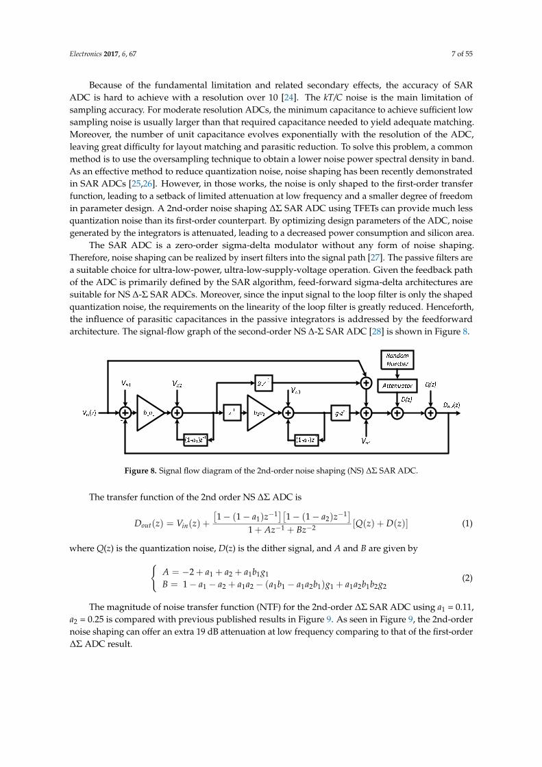
Because of the fundamental limitation and related secondary effects, the accuracy of SARADC is hard to achieve with a resolution over 10 [24]. The kT/C noise is the main limitation ofsampling accuracy. For moderate resolution ADCs, the minimum capacitance to achieve sufficient lowsampling noise is usually larger than that required capacitance needed to yield adequate matching.Moreover, the number of unit capacitance evolves exponentially with the resolution of the ADC,leaving great difficulty for layout matching and parasitic reduction. To solve this problem, a commonmethod is to use the oversampling technique to obtain a lower noise power spectral density in band.As an effective method to reduce quantization noise, noise shaping has been recently demonstratedin SAR ADCs [25,26]. However, in those works, the noise is only shaped to the first-order transferfunction, leading to a setback of limited attenuation at low frequency and a smaller degree of freedomin parameter design. A 2nd-order noise shaping ∆Σ SAR ADC using TFETs can provide much lessquantization noise than its first-order counterpart. By optimizing design parameters of the ADC, noisegenerated by the integrators is attenuated, leading to a decreased power consumption and silicon area.
The SAR ADC is a zero-order sigma-delta modulator without any form of noise shaping.Therefore, noise shaping can be realized by insert filters into the signal path [27]. The passive filters area suitable choice for ultra-low-power, ultra-low-supply-voltage operation. Given the feedback pathof the ADC is primarily defined by the SAR algorithm, feed-forward sigma-delta architectures aresuitable for NS ∆-Σ SAR ADCs. Moreover, since the input signal to the loop filter is only the shapedquantization noise, the requirements on the linearity of the loop filter is greatly reduced. Henceforth,the influence of parasitic capacitances in the passive integrators is addressed by the feedforwardarchitecture. The signal-flow graph of the second-order NS ∆-Σ SAR ADC [28] is shown in Figure 8.
Electronics 2017, 6, 67 7 of 54
Moreover, the number of unit capacitance evolves exponentially with the resolution of the ADC,
leaving great difficulty for layout matching and parasitic reduction. To solve this problem, a common
method is to use the oversampling technique to obtain a lower noise power spectral density in band.
As an effective method to reduce quantization noise, noise shaping has been recently demonstrated
in SAR ADCs [25,26]. However, in those works, the noise is only shaped to the first‐order transfer
function, leading to a setback of limited attenuation at low frequency and a smaller degree of freedom
in parameter design. A 2nd‐order noise shaping Δ� SAR ADC using TFETs can provide much less
quantization noise than its first‐order counterpart. By optimizing design parameters of the ADC,
noise generated by the integrators is attenuated, leading to a decreased power consumption and
silicon area.
The SAR ADC is a zero‐order sigma‐delta modulator without any form of noise shaping.
Therefore, noise shaping can be realized by insert filters into the signal path [27]. The passive filters
are a suitable choice for ultra‐low‐power, ultra‐low‐supply‐voltage operation. Given the feedback
path of the ADC is primarily defined by the SAR algorithm, feed‐forward sigma‐delta architectures
are suitable for NS Δ‐� SAR ADCs. Moreover, since the input signal to the loop filter is only the
shaped quantization noise, the requirements on the linearity of the loop filter is greatly reduced.
Henceforth, the influence of parasitic capacitances in the passive integrators is addressed by the
feedforward architecture. The signal‐flow graph of the second‐order NS Δ‐� SAR ADC [28] is shown
in Figure 8.
Figure 8. Signal flow diagram of the 2nd‐order noise shaping (NS) ΔƩ SAR ADC.
The transfer function of the 2nd order NS ΔƩ ADC is
1 1 1 11
(1)
where Q(z) is the quantization noise, D(z) is the dither signal, and A and B are given by
221211121112121
11121
)(1
2
gbbaagbaabaaaaaB
gbaaaA (2)
The magnitude of noise transfer function (NTF) for the 2nd‐order ΔƩ SAR ADC using a1 = 0.11, a2 = 0.25 is compared with previous published results in Figure 9. As seen in Figure 9, the 2nd‐order
noise shaping can offer an extra 19 dB attenuation at low frequency comparing to that of the first‐
order ΔƩ ADC result.
Figure 8. Signal flow diagram of the 2nd-order noise shaping (NS) ∆Σ SAR ADC.
The transfer function of the 2nd order NS ∆Σ ADC is
Dout(z) = Vin(z) +[1− (1− a1)z−1][1− (1− a2)z−1]
1 + Az−1 + Bz−2 [Q(z) + D(z)] (1)
where Q(z) is the quantization noise, D(z) is the dither signal, and A and B are given by{A = −2 + a1 + a2 + a1b1g1
B = 1− a1 − a2 + a1a2 − (a1b1 − a1a2b1)g1 + a1a2b1b2g2(2)
The magnitude of noise transfer function (NTF) for the 2nd-order ∆Σ SAR ADC using a1 = 0.11,a2 = 0.25 is compared with previous published results in Figure 9. As seen in Figure 9, the 2nd-ordernoise shaping can offer an extra 19 dB attenuation at low frequency comparing to that of the first-order∆Σ ADC result.
Electronics 2017, 6, 67 8 of 55Electronics 2017, 6, 67 8 of 54
0.01 0.1 1
-30
-20
-10
0
10
-31 dB
-6 dB
-12 dBN
TF
Mag
nitu
de (
dB)
Normalized Frequency (radians/sample)
(1 - 0.5z-1) VLSI15 [25] (1 - 0.75z-1) ESSCIRC16 [26] This work (1 - 0.75z-1)(1-0.89z-1)
Figure 9. Different noise transfer function (NTF) performance versus normalized frequency.
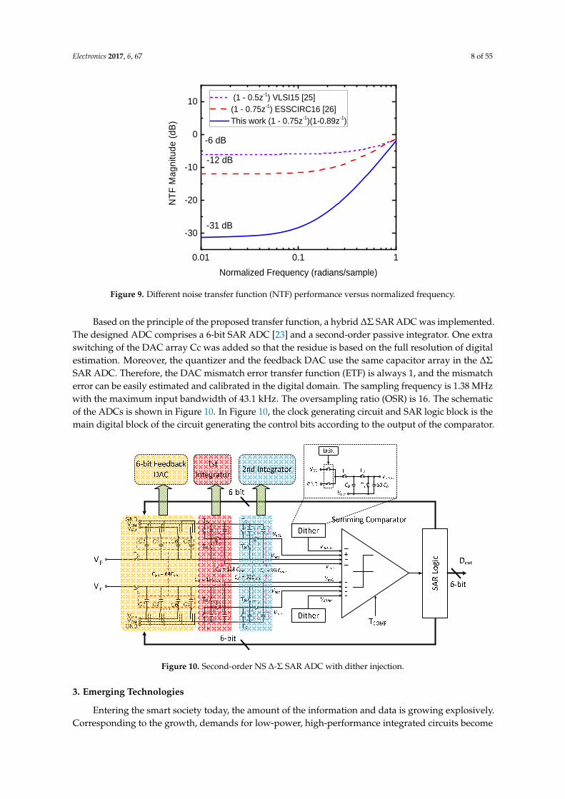
Based on the principle of the proposed transfer function, a hybrid Δ� SAR ADC was
implemented. The designed ADC comprises a 6‐bit SAR ADC [23] and a second‐order passive
integrator. One extra switching of the DAC array Cc was added so that the residue is based on the
full resolution of digital estimation. Moreover, the quantizer and the feedback DAC use the same
capacitor array in the Δ� SAR ADC. Therefore, the DAC mismatch error transfer function (ETF) is
always 1, and the mismatch error can be easily estimated and calibrated in the digital domain. The
sampling frequency is 1.38 MHz with the maximum input bandwidth of 43.1 kHz. The oversampling
ratio (OSR) is 16. The schematic of the ADCs is shown in Figure 10. In Figure 10, the clock generating
circuit and SAR logic block is the main digital block of the circuit generating the control bits according
to the output of the comparator.
Figure 10. Second‐order NS Δ‐� SAR ADC with dither injection.
Figure 9. Different noise transfer function (NTF) performance versus normalized frequency.
Based on the principle of the proposed transfer function, a hybrid ∆Σ SAR ADC was implemented.The designed ADC comprises a 6-bit SAR ADC [23] and a second-order passive integrator. One extraswitching of the DAC array Cc was added so that the residue is based on the full resolution of digitalestimation. Moreover, the quantizer and the feedback DAC use the same capacitor array in the ∆ΣSAR ADC. Therefore, the DAC mismatch error transfer function (ETF) is always 1, and the mismatcherror can be easily estimated and calibrated in the digital domain. The sampling frequency is 1.38 MHzwith the maximum input bandwidth of 43.1 kHz. The oversampling ratio (OSR) is 16. The schematicof the ADCs is shown in Figure 10. In Figure 10, the clock generating circuit and SAR logic block is themain digital block of the circuit generating the control bits according to the output of the comparator.
Electronics 2017, 6, 67 8 of 54
0.01 0.1 1
-30
-20
-10
0
10
-31 dB
-6 dB
-12 dB
NT
F M
agni
tude
(dB
)
Normalized Frequency (radians/sample)
(1 - 0.5z-1) VLSI15 [25] (1 - 0.75z-1) ESSCIRC16 [26] This work (1 - 0.75z-1)(1-0.89z-1)
Figure 9. Different noise transfer function (NTF) performance versus normalized frequency.
Based on the principle of the proposed transfer function, a hybrid Δ� SAR ADC was
implemented. The designed ADC comprises a 6‐bit SAR ADC [23] and a second‐order passive
integrator. One extra switching of the DAC array Cc was added so that the residue is based on the
full resolution of digital estimation. Moreover, the quantizer and the feedback DAC use the same
capacitor array in the Δ� SAR ADC. Therefore, the DAC mismatch error transfer function (ETF) is
always 1, and the mismatch error can be easily estimated and calibrated in the digital domain. The
sampling frequency is 1.38 MHz with the maximum input bandwidth of 43.1 kHz. The oversampling
ratio (OSR) is 16. The schematic of the ADCs is shown in Figure 10. In Figure 10, the clock generating
circuit and SAR logic block is the main digital block of the circuit generating the control bits according
to the output of the comparator.
Figure 10. Second‐order NS Δ‐� SAR ADC with dither injection.
Figure 10. Second-order NS ∆-Σ SAR ADC with dither injection.
3. Emerging Technologies
Entering the smart society today, the amount of the information and data is growing explosively.Corresponding to the growth, demands for low-power, high-performance integrated circuits become
Electronics 2017, 6, 67 9 of 55
even stronger. The slowdown of Moore’s law intensifies the search of the next transistor and memorytechnologies beyond CMOS.
3.1. Emerging Logic Devices
3.1.1. SiNW FET
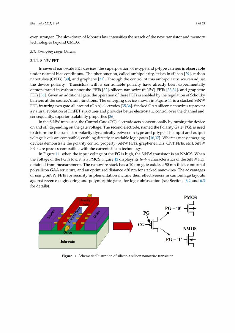
In several nanoscale FET devices, the superposition of n-type and p-type carriers is observableunder normal bias conditions. The phenomenon, called ambipolarity, exists in silicon [29], carbonnanotubes (CNTs) [30], and graphene [31]. Through the control of this ambipolarity, we can adjustthe device polarity. Transistors with a controllable polarity have already been experimentallydemonstrated in carbon nanotube FETs [32], silicon nanowire (SiNW) FETs [33,34], and grapheneFETs [35]. Given an additional gate, the operation of these FETs is enabled by the regulation of Schottkybarriers at the source/drain junctions. The emerging device shown in Figure 11 is a stacked SiNWFET, featuring two gate-all-around (GAA) electrodes [35,36]. Stacked GAA silicon nanowires representa natural evolution of FinFET structures and provides better electrostatic control over the channel and,consequently, superior scalability properties [36].
In the SiNW transistor, the Control Gate (CG) electrode acts conventionally by turning the deviceon and off, depending on the gate voltage. The second electrode, named the Polarity Gate (PG), is usedto determine the transistor polarity dynamically between n-type and p-type. The input and outputvoltage levels are compatible, enabling directly cascadable logic gates [36,37]. Whereas many emergingdevices demonstrate the polarity control property (SiNW FETs, graphene FETs, CNT FETs, etc.), SiNWFETs are process-compatible with the current silicon technology.
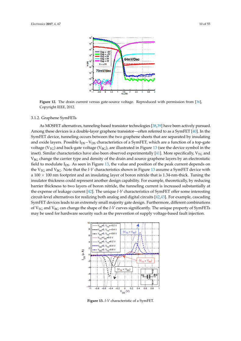
In Figure 11, when the input voltage of the PG is high, the SiNW transistor is an NMOS. Whenthe voltage of the PG is low, it is a PMOS. Figure 12 displays its ID-VG characteristics of the SiNW FETobtained from measurement. The nanowire stack has a 10 nm gate oxide, a 50 nm thick conformalpolysilicon GAA structure, and an optimized distance <20 nm for stacked nanowires. The advantagesof using SiNW FETs for security implementation include their effectiveness in camouflage layoutsagainst reverse-engineering and polymorphic gates for logic obfuscation (see Sections 6.2 and 6.3for details).
Electronics 2017, 6, 67 9 of 54
3. Emerging Technologies
Entering the smart society today, the amount of the information and data is growing explosively.
Corresponding to the growth, demands for low‐power, high‐performance integrated circuits become
even stronger. The slowdown of Moore’s law intensifies the search of the next transistor and memory
technologies beyond CMOS.
3.1. Emerging Logic Devices
3.1.1. SiNW FET
In several nanoscale FET devices, the superposition of n‐type and p‐type carriers is observable
under normal bias conditions. The phenomenon, called ambipolarity, exists in silicon [29], carbon
nanotubes (CNTs) [30], and graphene [31]. Through the control of this ambipolarity, we can adjust
the device polarity. Transistors with a controllable polarity have already been experimentally
demonstrated in carbon nanotube FETs [32], silicon nanowire (SiNW) FETs [33,34], and graphene
FETs [35]. Given an additional gate, the operation of these FETs is enabled by the regulation of
Schottky barriers at the source/drain junctions. The emerging device shown in Figure 11 is a stacked
SiNW FET, featuring two gate‐all‐around (GAA) electrodes [35,36]. Stacked GAA silicon nanowires
represent a natural evolution of FinFET structures and provides better electrostatic control over the
channel and, consequently, superior scalability properties [36].
In the SiNW transistor, the Control Gate (CG) electrode acts conventionally by turning the device
on and off, depending on the gate voltage. The second electrode, named the Polarity Gate (PG), is
used to determine the transistor polarity dynamically between n‐type and p‐type. The input and
output voltage levels are compatible, enabling directly cascadable logic gates [36,37]. Whereas many
emerging devices demonstrate the polarity control property (SiNW FETs, graphene FETs, CNT FETs,
etc.), SiNW FETs are process‐compatible with the current silicon technology.
In Figure 11, when the input voltage of the PG is high, the SiNW transistor is an NMOS. When
the voltage of the PG is low, it is a PMOS. Figure 12 displays its ID‐VG characteristics of the SiNW FET
obtained from measurement. The nanowire stack has a 10 nm gate oxide, a 50 nm thick conformal
polysilicon GAA structure, and an optimized distance <20 nm for stacked nanowires. The advantages of
using SiNW FETs for security implementation include their effectiveness in camouflage layouts against
reverse‐engineering and polymorphic gates for logic obfuscation (see Sections 6.2 and 6.3 for details).
Figure 11. Schematic illustration of silicon a silicon nanowire transistor. Figure 11. Schematic illustration of silicon a silicon nanowire transistor.
Electronics 2017, 6, 67 10 of 55
Electronics 2017, 6, 67 10 of 54
Figure 12. The drain current versus gate‐source voltage. Reproduced with permission from [36],
Copyright IEEE, 2012.
3.1.2. Graphene SymFETs
As MOSFET alternatives, tunneling‐based transistor technologies [38,39] have been actively
pursued. Among these devices is a double‐layer graphene transistor—often referred to as a SymFET
[40]. In the SymFET device, tunneling occurs between the two graphene sheets that are separated by
insulating and oxide layers. Possible IDS−VDS characteristics of a SymFET, which are a function of a
top‐gate voltage (VTG) and back‐gate voltage (VBG), are illustrated in Figure 13 (see the device symbol
in the inset). Similar characteristics have also been observed experimentally [41]. More specifically,
VTG and VBG change the carrier type and density of the drain and source graphene layers by an
electrostatic field to modulate IDS. As seen in Figure 13, the value and position of the peak current
depends on the VTG and VBG. Note that the I‐V characteristics shown in Figure 13 assume a SymFET
device with a 100 × 100 nm footprint and an insulating layer of boron nitride that is 1.34‐nm‐thick.
Tuning the insulator thickness could represent another design capability. For example, theoretically,
by reducing barrier thickness to two layers of boron nitride, the tunneling current is increased
substantially at the expense of leakage current [42]. The unique I‐V characteristics of SymFET offer
some interesting circuit‐level alternatives for realizing both analog and digital circuits [42,43]. For
example, cascading SymFET devices leads to an extremely small majority gate design. Furthermore,
different combinations of VTG and VBG can change the shape of the I‐V curves significantly. The unique
property of SymFETs may be used for hardware security such as the prevention of supply voltage‐
based fault injection.
Figure 13. I‐V characteristic of a SymFET.
Figure 12. The drain current versus gate-source voltage. Reproduced with permission from [36],Copyright IEEE, 2012.
3.1.2. Graphene SymFETs
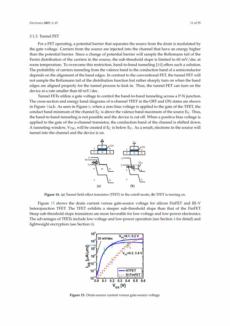
As MOSFET alternatives, tunneling-based transistor technologies [38,39] have been actively pursued.Among these devices is a double-layer graphene transistor—often referred to as a SymFET [40]. In theSymFET device, tunneling occurs between the two graphene sheets that are separated by insulatingand oxide layers. Possible IDS−VDS characteristics of a SymFET, which are a function of a top-gatevoltage (VTG) and back-gate voltage (VBG), are illustrated in Figure 13 (see the device symbol in theinset). Similar characteristics have also been observed experimentally [41]. More specifically, VTG andVBG change the carrier type and density of the drain and source graphene layers by an electrostaticfield to modulate IDS. As seen in Figure 13, the value and position of the peak current depends onthe VTG and VBG. Note that the I-V characteristics shown in Figure 13 assume a SymFET device witha 100 × 100 nm footprint and an insulating layer of boron nitride that is 1.34-nm-thick. Tuning theinsulator thickness could represent another design capability. For example, theoretically, by reducingbarrier thickness to two layers of boron nitride, the tunneling current is increased substantially atthe expense of leakage current [42]. The unique I-V characteristics of SymFET offer some interestingcircuit-level alternatives for realizing both analog and digital circuits [42,43]. For example, cascadingSymFET devices leads to an extremely small majority gate design. Furthermore, different combinationsof VTG and VBG can change the shape of the I-V curves significantly. The unique property of SymFETsmay be used for hardware security such as the prevention of supply voltage-based fault injection.
Electronics 2017, 6, 67 10 of 54
Figure 12. The drain current versus gate‐source voltage. Reproduced with permission from [36],
Copyright IEEE, 2012.
3.1.2. Graphene SymFETs
As MOSFET alternatives, tunneling‐based transistor technologies [38,39] have been actively
pursued. Among these devices is a double‐layer graphene transistor—often referred to as a SymFET
[40]. In the SymFET device, tunneling occurs between the two graphene sheets that are separated by
insulating and oxide layers. Possible IDS−VDS characteristics of a SymFET, which are a function of a
top‐gate voltage (VTG) and back‐gate voltage (VBG), are illustrated in Figure 13 (see the device symbol
in the inset). Similar characteristics have also been observed experimentally [41]. More specifically,
VTG and VBG change the carrier type and density of the drain and source graphene layers by an
electrostatic field to modulate IDS. As seen in Figure 13, the value and position of the peak current
depends on the VTG and VBG. Note that the I‐V characteristics shown in Figure 13 assume a SymFET
device with a 100 × 100 nm footprint and an insulating layer of boron nitride that is 1.34‐nm‐thick.
Tuning the insulator thickness could represent another design capability. For example, theoretically,
by reducing barrier thickness to two layers of boron nitride, the tunneling current is increased
substantially at the expense of leakage current [42]. The unique I‐V characteristics of SymFET offer
some interesting circuit‐level alternatives for realizing both analog and digital circuits [42,43]. For
example, cascading SymFET devices leads to an extremely small majority gate design. Furthermore,
different combinations of VTG and VBG can change the shape of the I‐V curves significantly. The unique
property of SymFETs may be used for hardware security such as the prevention of supply voltage‐
based fault injection.
Figure 13. I‐V characteristic of a SymFET. Figure 13. I-V characteristic of a SymFET.
Electronics 2017, 6, 67 11 of 55
3.1.3. Tunnel FET
For a FET operating, a potential barrier that separates the source from the drain is modulated bythe gate voltage. Carriers from the source are injected into the channel that have an energy higherthan the potential barrier. Since a change of potential barrier will sample the Boltzmann tail of theFermi distribution of the carriers in the source, the sub-threshold slope is limited to 60 mV/dec atroom temperature. To overcome this restriction, band-to-band tunneling [44] offers such a solution.The probability of carriers tunneling from the valence band to the conduction band of a semiconductordepends on the alignment of the band edges. In contrast to the conventional FET, the tunnel FET willnot sample the Boltzmann tail of the distribution function but rather sharply turn on when the bandedges are aligned properly for the tunnel process to kick in. Thus, the tunnel FET can turn on thedevice at a rate smaller than 60 mV/dec.
Tunnel FETs utilize a gate voltage to control the band-to-band tunneling across a P-N junction.The cross-section and energy band diagrams of n-channel TFET in the OFF and ON states are shownin Figure 14a,b. As seen in Figure 6, when a zero bias voltage is applied to the gate of the TFET, theconduct band minimum of the channel EC is above the valence band maximum of the source EV. Thus,the band-to-band tunneling is not possible and the device is cut off. When a positive bias voltage isapplied to the gate of the n-channel transistor, the conduction band of the channel is shifted down.A tunneling window, VTW, will be created if EC is below EV. As a result, electrons in the source willtunnel into the channel and the device is on.
Electronics 2017, 6, 67 11 of 54
3.1.3. Tunnel FET
For a FET operating, a potential barrier that separates the source from the drain is modulated by
the gate voltage. Carriers from the source are injected into the channel that have an energy higher
than the potential barrier. Since a change of potential barrier will sample the Boltzmann tail of the
Fermi distribution of the carriers in the source, the sub‐threshold slope is limited to 60 mV/dec at
room temperature. To overcome this restriction, band‐to‐band tunneling [44] offers such a solution.
The probability of carriers tunneling from the valence band to the conduction band of a
semiconductor depends on the alignment of the band edges. In contrast to the conventional FET, the
tunnel FET will not sample the Boltzmann tail of the distribution function but rather sharply turn on
when the band edges are aligned properly for the tunnel process to kick in. Thus, the tunnel FET can
turn on the device at a rate smaller than 60 mV/dec.
Tunnel FETs utilize a gate voltage to control the band‐to‐band tunneling across a P‐N junction.
The cross‐section and energy band diagrams of n‐channel TFET in the OFF and ON states are shown
in Figure 14a,b. As seen in Figure 6, when a zero bias voltage is applied to the gate of the TFET, the
conduct band minimum of the channel EC is above the valence band maximum of the source EV. Thus,
the band‐to‐band tunneling is not possible and the device is cut off. When a positive bias voltage is
applied to the gate of the n‐channel transistor, the conduction band of the channel is shifted down. A
tunneling window, VTW, will be created if EC is below EV. As a result, electrons in the source will
tunnel into the channel and the device is on.
G
P N‐ N
TOXS D
EC
EV
S D
No tunneling
P N‐ N
G
P N‐ N
TOXS D
EC
EV
S D
P N‐ N
VGS
qVTW
(a) (b)
Figure 14. (a) Tunnel field effect transistor (TFET) in the cutoff mode; (b) TFET is turning on.
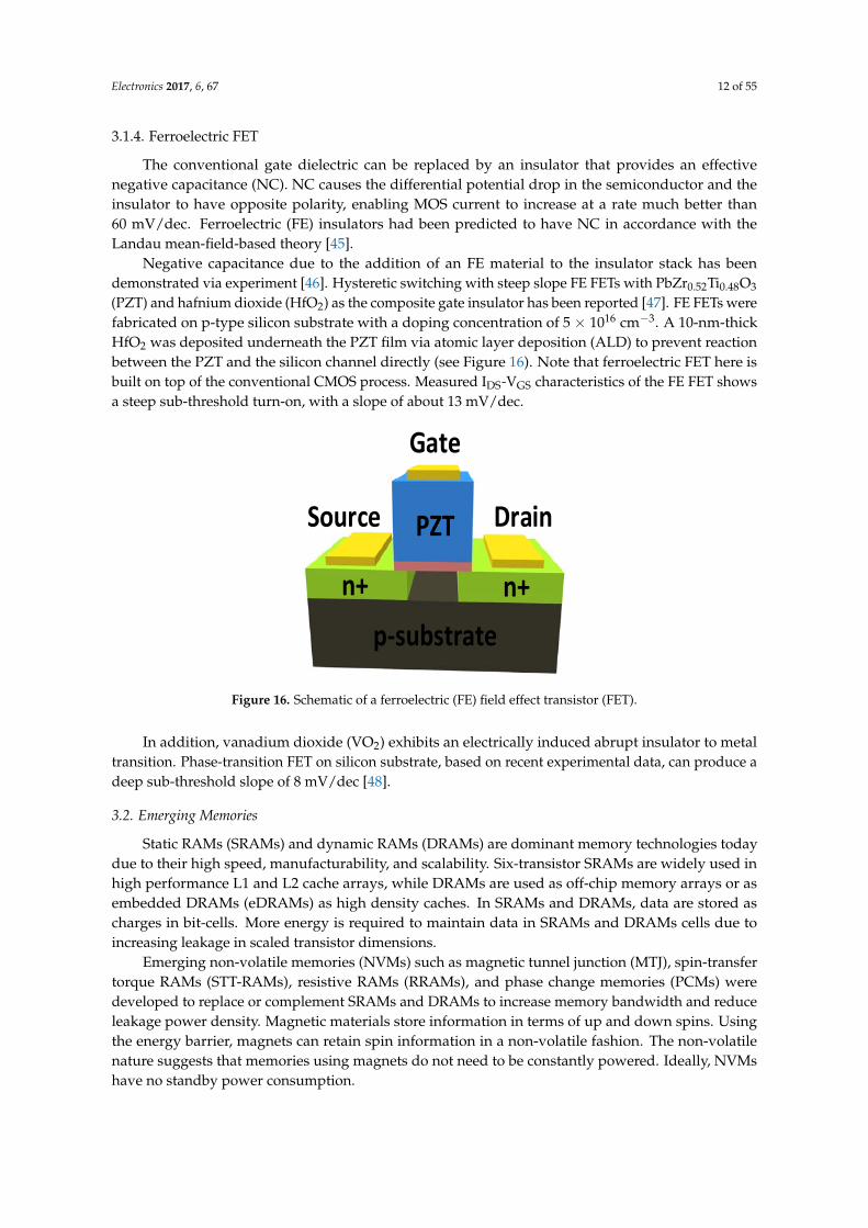
Figure 15 shows the drain current versus gate‐source voltage for silicon FinFET and III–V
heterojunction TFET. The TFET exhibits a steeper sub‐threshold slope than that of the FinFET. Steep
sub‐threshold slope transistors are more favorable for low‐voltage and low‐power electronics. The
advantages of TFETs include low‐voltage and low‐power operation (see Section 4 for detail) and
lightweight encryption (see Section 6).
Figure 14. (a) Tunnel field effect transistor (TFET) in the cutoff mode; (b) TFET is turning on.
Figure 15 shows the drain current versus gate-source voltage for silicon FinFET and III–Vheterojunction TFET. The TFET exhibits a steeper sub-threshold slope than that of the FinFET.Steep sub-threshold slope transistors are more favorable for low-voltage and low-power electronics.The advantages of TFETs include low-voltage and low-power operation (see Section 4 for detail) andlightweight encryption (see Section 6).Electronics 2017, 6, 67 12 of 54
Figure 15. Drain‐source current versus gate‐source voltage.
3.1.4. Ferroelectric FET
The conventional gate dielectric can be replaced by an insulator that provides an effective
negative capacitance (NC). NC causes the differential potential drop in the semiconductor and the
insulator to have opposite polarity, enabling MOS current to increase at a rate much better than 60
mV/dec. Ferroelectric (FE) insulators had been predicted to have NC in accordance with the Landau
mean‐field‐based theory [45].
Negative capacitance due to the addition of an FE material to the insulator stack has been
demonstrated via experiment [46]. Hysteretic switching with steep slope FE FETs with PbZr0.52Ti0.48O3
(PZT) and hafnium dioxide (HfO2) as the composite gate insulator has been reported [47]. FE FETs
were fabricated on p‐type silicon substrate with a doping concentration of 5 × 1016 cm−3. A 10‐nm‐
thick HfO2 was deposited underneath the PZT film via atomic layer deposition (ALD) to prevent
reaction between the PZT and the silicon channel directly (see Figure 16). Note that ferroelectric FET
here is built on top of the conventional CMOS process. Measured IDS‐VGS characteristics of the FE FET
shows a steep sub‐threshold turn‐on, with a slope of about 13 mV/dec.
p‐substrate
Gate
Source DrainPZT
n+ n+
Figure 16. Schematic of a ferroelectric (FE) field effect transistor (FET).
In addition, vanadium dioxide (VO2) exhibits an electrically induced abrupt insulator to metal
transition. Phase‐transition FET on silicon substrate, based on recent experimental data, can produce
a deep sub‐threshold slope of 8 mV/dec [48].
Figure 15. Drain-source current versus gate-source voltage.
Electronics 2017, 6, 67 12 of 55
3.1.4. Ferroelectric FET
The conventional gate dielectric can be replaced by an insulator that provides an effectivenegative capacitance (NC). NC causes the differential potential drop in the semiconductor and theinsulator to have opposite polarity, enabling MOS current to increase at a rate much better than60 mV/dec. Ferroelectric (FE) insulators had been predicted to have NC in accordance with theLandau mean-field-based theory [45].
Negative capacitance due to the addition of an FE material to the insulator stack has beendemonstrated via experiment [46]. Hysteretic switching with steep slope FE FETs with PbZr0.52Ti0.48O3
(PZT) and hafnium dioxide (HfO2) as the composite gate insulator has been reported [47]. FE FETs werefabricated on p-type silicon substrate with a doping concentration of 5 × 1016 cm−3. A 10-nm-thickHfO2 was deposited underneath the PZT film via atomic layer deposition (ALD) to prevent reactionbetween the PZT and the silicon channel directly (see Figure 16). Note that ferroelectric FET here isbuilt on top of the conventional CMOS process. Measured IDS-VGS characteristics of the FE FET showsa steep sub-threshold turn-on, with a slope of about 13 mV/dec.
Electronics 2017, 6, 67 12 of 54
Figure 15. Drain‐source current versus gate‐source voltage.
3.1.4. Ferroelectric FET
The conventional gate dielectric can be replaced by an insulator that provides an effective
negative capacitance (NC). NC causes the differential potential drop in the semiconductor and the
insulator to have opposite polarity, enabling MOS current to increase at a rate much better than 60
mV/dec. Ferroelectric (FE) insulators had been predicted to have NC in accordance with the Landau
mean‐field‐based theory [45].
Negative capacitance due to the addition of an FE material to the insulator stack has been
demonstrated via experiment [46]. Hysteretic switching with steep slope FE FETs with PbZr0.52Ti0.48O3
(PZT) and hafnium dioxide (HfO2) as the composite gate insulator has been reported [47]. FE FETs
were fabricated on p‐type silicon substrate with a doping concentration of 5 × 1016 cm−3. A 10‐nm‐
thick HfO2 was deposited underneath the PZT film via atomic layer deposition (ALD) to prevent
reaction between the PZT and the silicon channel directly (see Figure 16). Note that ferroelectric FET
here is built on top of the conventional CMOS process. Measured IDS‐VGS characteristics of the FE FET
shows a steep sub‐threshold turn‐on, with a slope of about 13 mV/dec.
p‐substrate
Gate
Source DrainPZT
n+ n+
Figure 16. Schematic of a ferroelectric (FE) field effect transistor (FET).
In addition, vanadium dioxide (VO2) exhibits an electrically induced abrupt insulator to metal
transition. Phase‐transition FET on silicon substrate, based on recent experimental data, can produce
a deep sub‐threshold slope of 8 mV/dec [48].
Figure 16. Schematic of a ferroelectric (FE) field effect transistor (FET).
In addition, vanadium dioxide (VO2) exhibits an electrically induced abrupt insulator to metaltransition. Phase-transition FET on silicon substrate, based on recent experimental data, can produce adeep sub-threshold slope of 8 mV/dec [48].
3.2. Emerging Memories
Static RAMs (SRAMs) and dynamic RAMs (DRAMs) are dominant memory technologies todaydue to their high speed, manufacturability, and scalability. Six-transistor SRAMs are widely used inhigh performance L1 and L2 cache arrays, while DRAMs are used as off-chip memory arrays or asembedded DRAMs (eDRAMs) as high density caches. In SRAMs and DRAMs, data are stored ascharges in bit-cells. More energy is required to maintain data in SRAMs and DRAMs cells due toincreasing leakage in scaled transistor dimensions.
Emerging non-volatile memories (NVMs) such as magnetic tunnel junction (MTJ), spin-transfertorque RAMs (STT-RAMs), resistive RAMs (RRAMs), and phase change memories (PCMs) weredeveloped to replace or complement SRAMs and DRAMs to increase memory bandwidth and reduceleakage power density. Magnetic materials store information in terms of up and down spins. Usingthe energy barrier, magnets can retain spin information in a non-volatile fashion. The non-volatilenature suggests that memories using magnets do not need to be constantly powered. Ideally, NVMshave no standby power consumption.
Electronics 2017, 6, 67 13 of 55
3.2.1. Resistive Memory
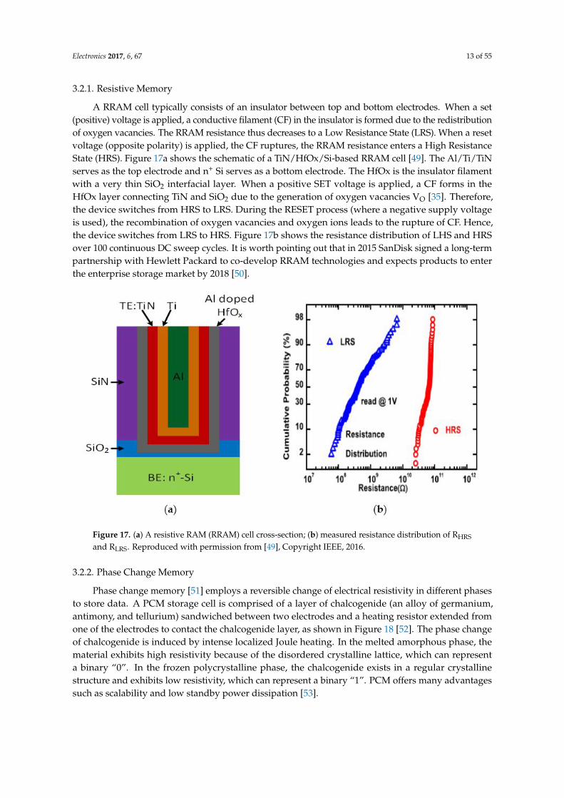
A RRAM cell typically consists of an insulator between top and bottom electrodes. When a set(positive) voltage is applied, a conductive filament (CF) in the insulator is formed due to the redistributionof oxygen vacancies. The RRAM resistance thus decreases to a Low Resistance State (LRS). When a resetvoltage (opposite polarity) is applied, the CF ruptures, the RRAM resistance enters a High ResistanceState (HRS). Figure 17a shows the schematic of a TiN/HfOx/Si-based RRAM cell [49]. The Al/Ti/TiNserves as the top electrode and n+ Si serves as a bottom electrode. The HfOx is the insulator filamentwith a very thin SiO2 interfacial layer. When a positive SET voltage is applied, a CF forms in theHfOx layer connecting TiN and SiO2 due to the generation of oxygen vacancies VO [35]. Therefore,the device switches from HRS to LRS. During the RESET process (where a negative supply voltageis used), the recombination of oxygen vacancies and oxygen ions leads to the rupture of CF. Hence,the device switches from LRS to HRS. Figure 17b shows the resistance distribution of LHS and HRSover 100 continuous DC sweep cycles. It is worth pointing out that in 2015 SanDisk signed a long-termpartnership with Hewlett Packard to co-develop RRAM technologies and expects products to enterthe enterprise storage market by 2018 [50].
Figure 17. (a) A resistive RAM (RRAM) cell cross-section; (b) measured resistance distribution of RHRS
and RLRS. Reproduced with permission from [49], Copyright IEEE, 2016.
3.2.2. Phase Change Memory
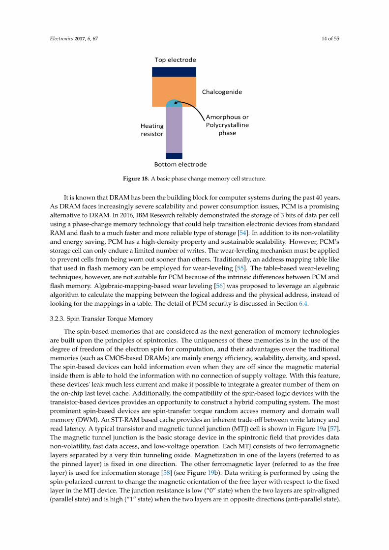
Phase change memory [51] employs a reversible change of electrical resistivity in different phasesto store data. A PCM storage cell is comprised of a layer of chalcogenide (an alloy of germanium,antimony, and tellurium) sandwiched between two electrodes and a heating resistor extended fromone of the electrodes to contact the chalcogenide layer, as shown in Figure 18 [52]. The phase changeof chalcogenide is induced by intense localized Joule heating. In the melted amorphous phase, thematerial exhibits high resistivity because of the disordered crystalline lattice, which can representa binary “0”. In the frozen polycrystalline phase, the chalcogenide exists in a regular crystallinestructure and exhibits low resistivity, which can represent a binary “1”. PCM offers many advantagessuch as scalability and low standby power dissipation [53].
Electronics 2017, 6, 67 14 of 55
Electronics 2017, 6, 67 14 of 54
3.2.2. Phase Change Memory
Phase change memory [51] employs a reversible change of electrical resistivity in different
phases to store data. A PCM storage cell is comprised of a layer of chalcogenide (an alloy of
germanium, antimony, and tellurium) sandwiched between two electrodes and a heating resistor
extended from one of the electrodes to contact the chalcogenide layer, as shown in Figure 18 [52]. The
phase change of chalcogenide is induced by intense localized Joule heating. In the melted amorphous
phase, the material exhibits high resistivity because of the disordered crystalline lattice, which can
represent a binary “0”. In the frozen polycrystalline phase, the chalcogenide exists in a regular
crystalline structure and exhibits low resistivity, which can represent a binary “1”. PCM offers many
advantages such as scalability and low standby power dissipation [53].
Top electrode
Amorphous or Polycrystalline
phase
Bottom electrode
Chalcogenide
Heating resistor
Figure 18. A basic phase change memory cell structure.
It is known that DRAM has been the building block for computer systems during the past 40
years. As DRAM faces increasingly severe scalability and power consumption issues, PCM is a
promising alternative to DRAM. In 2016, IBM Research reliably demonstrated the storage of 3 bits of
data per cell using a phase‐change memory technology that could help transition electronic devices
from standard RAM and flash to a much faster and more reliable type of storage [54]. In addition to
its non‐volatility and energy saving, PCM has a high‐density property and sustainable scalability.
However, PCM’s storage cell can only endure a limited number of writes. The wear‐leveling
mechanism must be applied to prevent cells from being worn out sooner than others. Traditionally,
an address mapping table like that used in flash memory can be employed for wear‐leveling [55]. The
table‐based wear‐leveling techniques, however, are not suitable for PCM because of the intrinsic
differences between PCM and flash memory. Algebraic‐mapping‐based wear leveling [56] was
proposed to leverage an algebraic algorithm to calculate the mapping between the logical address
and the physical address, instead of looking for the mappings in a table. The detail of PCM security
is discussed in Section 6.4.
3.2.3. Spin Transfer Torque Memory
The spin‐based memories that are considered as the next generation of memory technologies are
built upon the principles of spintronics. The uniqueness of these memories is in the use of the degree
of freedom of the electron spin for computation, and their advantages over the traditional memories
(such as CMOS‐based DRAMs) are mainly energy efficiency, scalability, density, and speed. The spin‐
based devices can hold information even when they are off since the magnetic material inside them
is able to hold the information with no connection of supply voltage. With this feature, these devicesʹ
leak much less current and make it possible to integrate a greater number of them on the on‐chip last
level cache. Additionally, the compatibility of the spin‐based logic devices with the transistor‐based
devices provides an opportunity to construct a hybrid computing system. The most prominent spin‐
based devices are spin‐transfer torque random access memory and domain wall memory (DWM).
Figure 18. A basic phase change memory cell structure.
It is known that DRAM has been the building block for computer systems during the past 40 years.As DRAM faces increasingly severe scalability and power consumption issues, PCM is a promisingalternative to DRAM. In 2016, IBM Research reliably demonstrated the storage of 3 bits of data per cellusing a phase-change memory technology that could help transition electronic devices from standardRAM and flash to a much faster and more reliable type of storage [54]. In addition to its non-volatilityand energy saving, PCM has a high-density property and sustainable scalability. However, PCM’sstorage cell can only endure a limited number of writes. The wear-leveling mechanism must be appliedto prevent cells from being worn out sooner than others. Traditionally, an address mapping table likethat used in flash memory can be employed for wear-leveling [55]. The table-based wear-levelingtechniques, however, are not suitable for PCM because of the intrinsic differences between PCM andflash memory. Algebraic-mapping-based wear leveling [56] was proposed to leverage an algebraicalgorithm to calculate the mapping between the logical address and the physical address, instead oflooking for the mappings in a table. The detail of PCM security is discussed in Section 6.4.
3.2.3. Spin Transfer Torque Memory
The spin-based memories that are considered as the next generation of memory technologiesare built upon the principles of spintronics. The uniqueness of these memories is in the use of thedegree of freedom of the electron spin for computation, and their advantages over the traditionalmemories (such as CMOS-based DRAMs) are mainly energy efficiency, scalability, density, and speed.The spin-based devices can hold information even when they are off since the magnetic materialinside them is able to hold the information with no connection of supply voltage. With this feature,these devices' leak much less current and make it possible to integrate a greater number of them onthe on-chip last level cache. Additionally, the compatibility of the spin-based logic devices with thetransistor-based devices provides an opportunity to construct a hybrid computing system. The mostprominent spin-based devices are spin-transfer torque random access memory and domain wallmemory (DWM). An STT-RAM based cache provides an inherent trade-off between write latency andread latency. A typical transistor and magnetic tunnel junction (MTJ) cell is shown in Figure 19a [57].The magnetic tunnel junction is the basic storage device in the spintronic field that provides datanon-volatility, fast data access, and low-voltage operation. Each MTJ consists of two ferromagneticlayers separated by a very thin tunneling oxide. Magnetization in one of the layers (referred to asthe pinned layer) is fixed in one direction. The other ferromagnetic layer (referred to as the freelayer) is used for information storage [58] (see Figure 19b). Data writing is performed by using thespin-polarized current to change the magnetic orientation of the free layer with respect to the fixedlayer in the MTJ device. The junction resistance is low (“0” state) when the two layers are spin-aligned(parallel state) and is high (“1” state) when the two layers are in opposite directions (anti-parallel state).
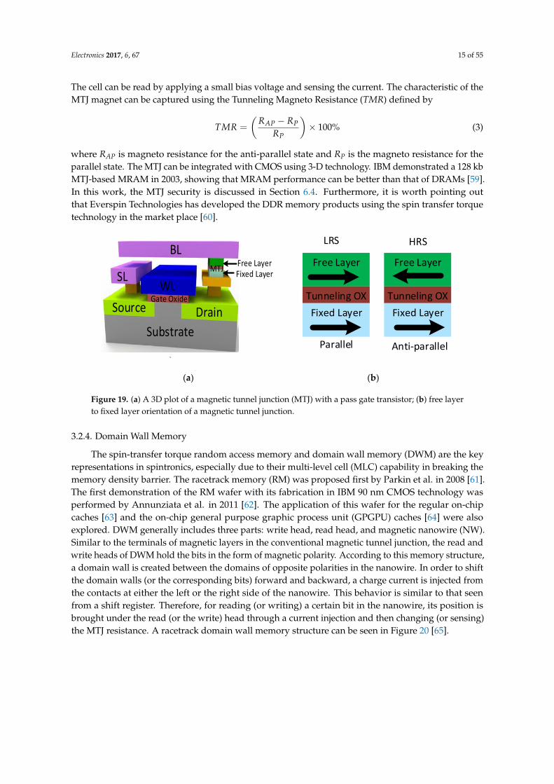
Electronics 2017, 6, 67 15 of 55
The cell can be read by applying a small bias voltage and sensing the current. The characteristic of theMTJ magnet can be captured using the Tunneling Magneto Resistance (TMR) defined by
TMR =
(RAP − RP
RP
)× 100% (3)
where RAP is magneto resistance for the anti-parallel state and RP is the magneto resistance for theparallel state. The MTJ can be integrated with CMOS using 3-D technology. IBM demonstrated a 128 kbMTJ-based MRAM in 2003, showing that MRAM performance can be better than that of DRAMs [59].In this work, the MTJ security is discussed in Section 6.4. Furthermore, it is worth pointing outthat Everspin Technologies has developed the DDR memory products using the spin transfer torquetechnology in the market place [60].
Electronics 2017, 6, 67 15 of 54
An STT‐RAM based cache provides an inherent trade‐off between write latency and read latency. A
typical transistor and magnetic tunnel junction (MTJ) cell is shown in Figure 19a [57]. The magnetic
tunnel junction is the basic storage device in the spintronic field that provides data non‐volatility, fast
data access, and low‐voltage operation. Each MTJ consists of two ferromagnetic layers separated by
a very thin tunneling oxide. Magnetization in one of the layers (referred to as the pinned layer) is
fixed in one direction. The other ferromagnetic layer (referred to as the free layer) is used for
information storage [58] (see Figure 19b). Data writing is performed by using the spin‐polarized
current to change the magnetic orientation of the free layer with respect to the fixed layer in the MTJ
device. The junction resistance is low (‘0” state) when the two layers are spin‐aligned (parallel state)
and is high (“1” state) when the two layers are in opposite directions (anti‐parallel state). The cell can
be read by applying a small bias voltage and sensing the current. The characteristic of the MTJ magnet
can be captured using the Tunneling Magneto Resistance (TMR) defined by
%100
P
PAP
R
RRTMR (3)
where RAP is magneto resistance for the anti‐parallel state and RP is the magneto resistance for the
parallel state. The MTJ can be integrated with CMOS using 3‐D technology. IBM demonstrated a 128
kb MTJ‐based MRAM in 2003, showing that MRAM performance can be better than that of DRAMs
[59]. In this work, the MTJ security is discussed in Section 6.4. Furthermore, it is worth pointing out
that Everspin Technologies has developed the DDR memory products using the spin transfer torque
technology in the market place [60].
`
Substrate
Source DrainGate OxideWL
SL
BLFree LayerFixed Layer
MTJ
Free Layer Free Layer
Fixed Layer Fixed Layer
Tunneling OX Tunneling OX
Parallel Anti‐parallel
LRS HRS
(a) (b)
Figure 19. (a) A 3D plot of a magnetic tunnel junction (MTJ) with a pass gate transistor; (b) free layer
to fixed layer orientation of a magnetic tunnel junction.
3.2.4. Domain Wall Memory
The spin‐transfer torque random access memory and domain wall memory (DWM) are the key
representations in spintronics, especially due to their multi‐level cell (MLC) capability in breaking
the memory density barrier. The racetrack memory (RM) was proposed first by Parkin et al. in 2008
[61]. The first demonstration of the RM wafer with its fabrication in IBM 90 nm CMOS technology
was performed by Annunziata et al. in 2011 [62]. The application of this wafer for the regular on‐chip
caches [63] and the on‐chip general purpose graphic process unit (GPGPU) caches [64] were also
explored. DWM generally includes three parts: write head, read head, and magnetic nanowire (NW).
Similar to the terminals of magnetic layers in the conventional magnetic tunnel junction, the read and
write heads of DWM hold the bits in the form of magnetic polarity. According to this memory
structure, a domain wall is created between the domains of opposite polarities in the nanowire. In
order to shift the domain walls (or the corresponding bits) forward and backward, a charge current
is injected from the contacts at either the left or the right side of the nanowire. This behavior is similar
to that seen from a shift register. Therefore, for reading (or writing) a certain bit in the nanowire, its
Figure 19. (a) A 3D plot of a magnetic tunnel junction (MTJ) with a pass gate transistor; (b) free layerto fixed layer orientation of a magnetic tunnel junction.
3.2.4. Domain Wall Memory
The spin-transfer torque random access memory and domain wall memory (DWM) are the keyrepresentations in spintronics, especially due to their multi-level cell (MLC) capability in breaking thememory density barrier. The racetrack memory (RM) was proposed first by Parkin et al. in 2008 [61].The first demonstration of the RM wafer with its fabrication in IBM 90 nm CMOS technology wasperformed by Annunziata et al. in 2011 [62]. The application of this wafer for the regular on-chipcaches [63] and the on-chip general purpose graphic process unit (GPGPU) caches [64] were alsoexplored. DWM generally includes three parts: write head, read head, and magnetic nanowire (NW).Similar to the terminals of magnetic layers in the conventional magnetic tunnel junction, the read andwrite heads of DWM hold the bits in the form of magnetic polarity. According to this memory structure,a domain wall is created between the domains of opposite polarities in the nanowire. In order to shiftthe domain walls (or the corresponding bits) forward and backward, a charge current is injected fromthe contacts at either the left or the right side of the nanowire. This behavior is similar to that seenfrom a shift register. Therefore, for reading (or writing) a certain bit in the nanowire, its position isbrought under the read (or the write) head through a current injection and then changing (or sensing)the MTJ resistance. A racetrack domain wall memory structure can be seen in Figure 20 [65].
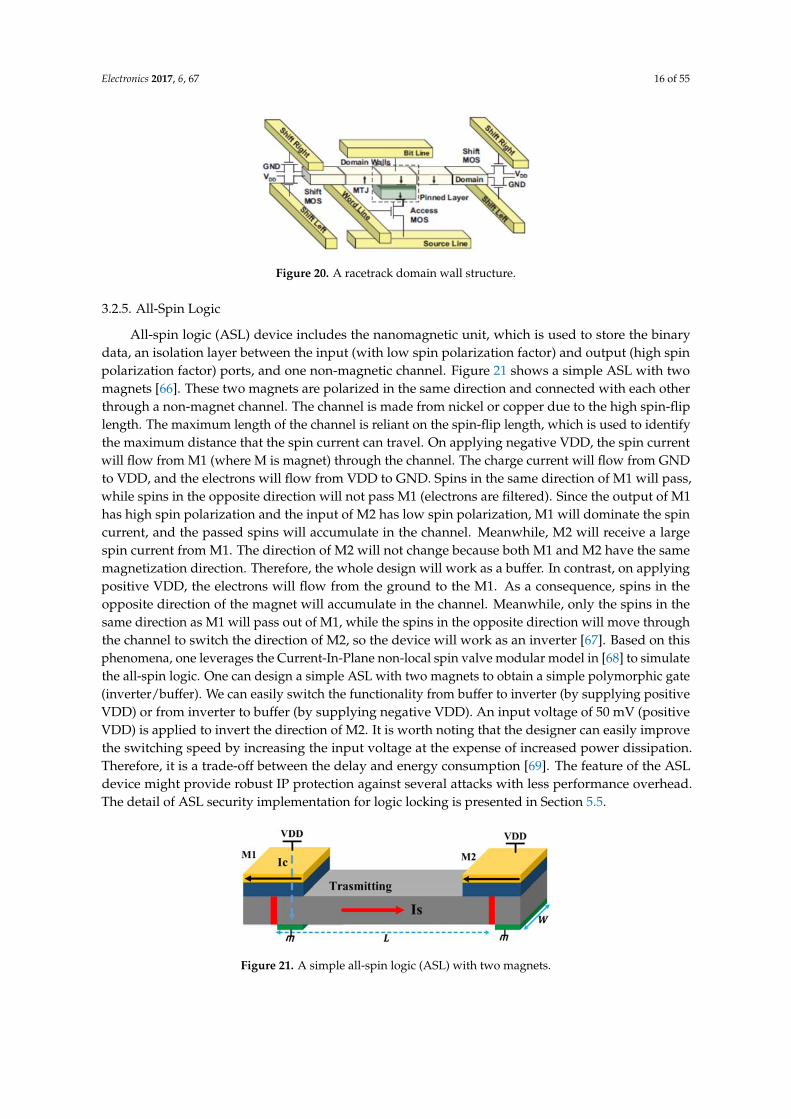
Electronics 2017, 6, 67 16 of 55
Electronics 2017, 6, 67 16 of 54
position is brought under the read (or the write) head through a current injection and then changing
(or sensing) the MTJ resistance. A racetrack domain wall memory structure can be seen in Figure 20
[65].
Figure 20. A racetrack domain wall structure.
3.2.5. All‐Spin Logic
All‐spin logic (ASL) device includes the nanomagnetic unit, which is used to store the binary
data, an isolation layer between the input (with low spin polarization factor) and output (high spin
polarization factor) ports, and one non‐magnetic channel. Figure 21 shows a simple ASL with two
magnets [66]. These two magnets are polarized in the same direction and connected with each other
through a non‐magnet channel. The channel is made from nickel or copper due to the high spin‐flip
length. The maximum length of the channel is reliant on the spin‐flip length, which is used to identify
the maximum distance that the spin current can travel. On applying negative VDD, the spin current
will flow from M1 (where M is magnet) through the channel. The charge current will flow from GND
to VDD, and the electrons will flow from VDD to GND. Spins in the same direction of M1 will pass,
while spins in the opposite direction will not pass M1 (electrons are filtered). Since the output of M1
has high spin polarization and the input of M2 has low spin polarization, M1 will dominate the spin
current, and the passed spins will accumulate in the channel. Meanwhile, M2 will receive a large spin
current from M1. The direction of M2 will not change because both M1 and M2 have the same
magnetization direction. Therefore, the whole design will work as a buffer. In contrast, on applying
positive VDD, the electrons will flow from the ground to the M1. As a consequence, spins in the
opposite direction of the magnet will accumulate in the channel. Meanwhile, only the spins in the
same direction as M1 will pass out of M1, while the spins in the opposite direction will move through
the channel to switch the direction of M2, so the device will work as an inverter [67]. Based on this
phenomena, one leverages the Current‐In‐Plane non‐local spin valve modular model in [68] to
simulate the all‐spin logic. One can design a simple ASL with two magnets to obtain a simple
polymorphic gate (inverter/buffer). We can easily switch the functionality from buffer to inverter (by
supplying positive VDD) or from inverter to buffer (by supplying negative VDD). An input voltage
of 50 mV (positive VDD) is applied to invert the direction of M2. It is worth noting that the designer
can easily improve the switching speed by increasing the input voltage at the expense of increased
power dissipation. Therefore, it is a trade‐off between the delay and energy consumption [69]. The
feature of the ASL device might provide robust IP protection against several attacks with less
performance overhead. The detail of ASL security implementation for logic locking is presented in
Section 5.5.
Figure 21. A simple all‐spin logic (ASL) with two magnets.
Figure 20. A racetrack domain wall structure.
3.2.5. All-Spin Logic
All-spin logic (ASL) device includes the nanomagnetic unit, which is used to store the binarydata, an isolation layer between the input (with low spin polarization factor) and output (high spinpolarization factor) ports, and one non-magnetic channel. Figure 21 shows a simple ASL with twomagnets [66]. These two magnets are polarized in the same direction and connected with each otherthrough a non-magnet channel. The channel is made from nickel or copper due to the high spin-fliplength. The maximum length of the channel is reliant on the spin-flip length, which is used to identifythe maximum distance that the spin current can travel. On applying negative VDD, the spin currentwill flow from M1 (where M is magnet) through the channel. The charge current will flow from GNDto VDD, and the electrons will flow from VDD to GND. Spins in the same direction of M1 will pass,while spins in the opposite direction will not pass M1 (electrons are filtered). Since the output of M1has high spin polarization and the input of M2 has low spin polarization, M1 will dominate the spincurrent, and the passed spins will accumulate in the channel. Meanwhile, M2 will receive a largespin current from M1. The direction of M2 will not change because both M1 and M2 have the samemagnetization direction. Therefore, the whole design will work as a buffer. In contrast, on applyingpositive VDD, the electrons will flow from the ground to the M1. As a consequence, spins in theopposite direction of the magnet will accumulate in the channel. Meanwhile, only the spins in thesame direction as M1 will pass out of M1, while the spins in the opposite direction will move throughthe channel to switch the direction of M2, so the device will work as an inverter [67]. Based on thisphenomena, one leverages the Current-In-Plane non-local spin valve modular model in [68] to simulatethe all-spin logic. One can design a simple ASL with two magnets to obtain a simple polymorphic gate(inverter/buffer). We can easily switch the functionality from buffer to inverter (by supplying positiveVDD) or from inverter to buffer (by supplying negative VDD). An input voltage of 50 mV (positiveVDD) is applied to invert the direction of M2. It is worth noting that the designer can easily improvethe switching speed by increasing the input voltage at the expense of increased power dissipation.Therefore, it is a trade-off between the delay and energy consumption [69]. The feature of the ASLdevice might provide robust IP protection against several attacks with less performance overhead.The detail of ASL security implementation for logic locking is presented in Section 5.5.
Electronics 2017, 6, 67 16 of 54
position is brought under the read (or the write) head through a current injection and then changing
(or sensing) the MTJ resistance. A racetrack domain wall memory structure can be seen in Figure 20
[65].
Figure 20. A racetrack domain wall structure.
3.2.5. All‐Spin Logic
All‐spin logic (ASL) device includes the nanomagnetic unit, which is used to store the binary
data, an isolation layer between the input (with low spin polarization factor) and output (high spin
polarization factor) ports, and one non‐magnetic channel. Figure 21 shows a simple ASL with two
magnets [66]. These two magnets are polarized in the same direction and connected with each other
through a non‐magnet channel. The channel is made from nickel or copper due to the high spin‐flip
length. The maximum length of the channel is reliant on the spin‐flip length, which is used to identify
the maximum distance that the spin current can travel. On applying negative VDD, the spin current
will flow from M1 (where M is magnet) through the channel. The charge current will flow from GND
to VDD, and the electrons will flow from VDD to GND. Spins in the same direction of M1 will pass,
while spins in the opposite direction will not pass M1 (electrons are filtered). Since the output of M1
has high spin polarization and the input of M2 has low spin polarization, M1 will dominate the spin
current, and the passed spins will accumulate in the channel. Meanwhile, M2 will receive a large spin
current from M1. The direction of M2 will not change because both M1 and M2 have the same
magnetization direction. Therefore, the whole design will work as a buffer. In contrast, on applying
positive VDD, the electrons will flow from the ground to the M1. As a consequence, spins in the
opposite direction of the magnet will accumulate in the channel. Meanwhile, only the spins in the
same direction as M1 will pass out of M1, while the spins in the opposite direction will move through
the channel to switch the direction of M2, so the device will work as an inverter [67]. Based on this
phenomena, one leverages the Current‐In‐Plane non‐local spin valve modular model in [68] to
simulate the all‐spin logic. One can design a simple ASL with two magnets to obtain a simple
polymorphic gate (inverter/buffer). We can easily switch the functionality from buffer to inverter (by
supplying positive VDD) or from inverter to buffer (by supplying negative VDD). An input voltage
of 50 mV (positive VDD) is applied to invert the direction of M2. It is worth noting that the designer
can easily improve the switching speed by increasing the input voltage at the expense of increased
power dissipation. Therefore, it is a trade‐off between the delay and energy consumption [69]. The
feature of the ASL device might provide robust IP protection against several attacks with less
performance overhead. The detail of ASL security implementation for logic locking is presented in
Section 5.5.
Figure 21. A simple all‐spin logic (ASL) with two magnets. Figure 21. A simple all-spin logic (ASL) with two magnets.
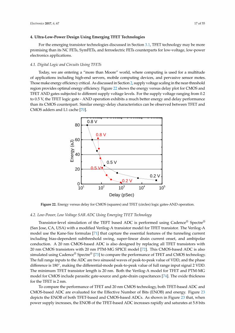
Electronics 2017, 6, 67 17 of 55
4. Ultra-Low-Power Design Using Emerging TFET Technologies
For the emerging transistor technologies discussed in Section 3.1, TFET technology may be morepromising than its NC FETs, SymFETs, and ferroelectric FETs counterparts for low-voltage, low-powerelectronics applications.
4.1. Digital Logic and Circuits Using TFETs
Today, we are entering a “more than Moore” world, where computing is used for a multitudeof applications including high-end servers, mobile computing devices, and pervasive sensor motes.Those make energy efficiency critical. As discussed in Section 2, supply voltage scaling in the near-thresholdregion provides optimal energy efficiency. Figure 22 shows the energy versus delay plot for CMOS andTFET AND gates subjected to different supply voltage levels. For the supply voltage ranging from 0.2to 0.5 V, the TFET logic gate - AND operation exhibits a much better energy and delay performancethan its CMOS counterpart. Similar energy-delay characteristics can be observed between TFET andCMOS adders and L1 cache [70].
Electronics 2017, 6, 67 17 of 54
4. Ultra‐Low‐Power Design Using Emerging TFET Technologies
For the emerging transistor technologies discussed in Section 3.1, TFET technology may be more
promising than its NC FETs, SymFETs, and ferroelectric FETs counterparts for low‐voltage, low‐
power electronics applications.
4.1. Digital Logic and Circuits Using TFETs
Today, we are entering a “more than Moore” world, where computing is used for a multitude
of applications including high‐end servers, mobile computing devices, and pervasive sensor motes.
Those make energy efficiency critical. As discussed in Section 2, supply voltage scaling in the near‐
threshold region provides optimal energy efficiency. Figure 22 shows the energy versus delay plot
for CMOS and TFET AND gates subjected to different supply voltage levels. For the supply voltage
ranging from 0.2 to 0.5 V, the TFET logic gate ‐ AND operation exhibits a much better energy and
delay performance than its CMOS counterpart. Similar energy‐delay characteristics can be observed
between TFET and CMOS adders and L1 cache [70].
101 102 103 104 1050
20
40
60
80
0.2 V
0.5 V
0.2 V
0.5 V
0.8 V
Ene
rgy
(aJ)
Delay (pSec)
0.8 V
Figure 22. Energy versus delay for CMOS (squares) and TFET (circles) logic gates ‐ AND operation.
4.2. Low‐Power, Low Voltage SAR ADC Using Emerging TFET Technology
Transistor‐level simulation of the TEFT based ADC is performed using Cadence® Spectre® (San
Jose, CA, USA) with a modified Verilog‐A transistor model for TFET transistor. The Verilog‐A model
use the Kane‐Sze formulas [71] that capture the essential features of the tunneling current including
bias‐dependent subthreshold swing, super‐linear drain current onset, and ambipolar conduction. A
20 nm CMOS‐based ADC is also designed by replacing all TFET transistors with 20 nm CMOS
transistors with 20 nm PTM‐MG SPICE model [72]. This CMOS‐based ADC is also simulated using
Cadence® Spectre® [73] to compare the performance of TFET and CMOS technology. The full range
inputs to the ADC are two sinusoid waves of peak‐to‐peak value of VDD, and the phase difference
is 180°, making the differential‐mode peak‐to‐peak value of full range input signal 2 VDD. The
minimum TFET transistor length is 20 nm. Both the Verilog‐A model for TFET and PTM‐MG model
for CMOS include parasitic gate‐source and gate‐drain capacitances [74]. The oxide thickness for the
TFET is 2 nm.
To compare the performance of TFET and 20 nm CMOS technology, both TFET‐based ADC and
CMOS‐based ADC are evaluated for the Effective Number of Bits (ENOB) and energy. Figure 23
depicts the ENOB of both TFET‐based and CMOS‐based ADCs. As shown in Figure 23 that, when
power supply increases, the ENOB of the TFET‐based ADC increases rapidly and saturates at 5.8 bits
when VDD is above 0.5 V. At a same supply voltage, the TFET‐based ADC shows better ENOB than
Figure 22. Energy versus delay for CMOS (squares) and TFET (circles) logic gates-AND operation.
4.2. Low-Power, Low Voltage SAR ADC Using Emerging TFET Technology
Transistor-level simulation of the TEFT based ADC is performed using Cadence® Spectre®
(San Jose, CA, USA) with a modified Verilog-A transistor model for TFET transistor. The Verilog-Amodel use the Kane-Sze formulas [71] that capture the essential features of the tunneling currentincluding bias-dependent subthreshold swing, super-linear drain current onset, and ambipolarconduction. A 20 nm CMOS-based ADC is also designed by replacing all TFET transistors with20 nm CMOS transistors with 20 nm PTM-MG SPICE model [72]. This CMOS-based ADC is alsosimulated using Cadence® Spectre® [73] to compare the performance of TFET and CMOS technology.The full range inputs to the ADC are two sinusoid waves of peak-to-peak value of VDD, and the phasedifference is 180◦, making the differential-mode peak-to-peak value of full range input signal 2 VDD.The minimum TFET transistor length is 20 nm. Both the Verilog-A model for TFET and PTM-MGmodel for CMOS include parasitic gate-source and gate-drain capacitances [74]. The oxide thicknessfor the TFET is 2 nm.
To compare the performance of TFET and 20 nm CMOS technology, both TFET-based ADC andCMOS-based ADC are evaluated for the Effective Number of Bits (ENOB) and energy. Figure 23depicts the ENOB of both TFET-based and CMOS-based ADCs. As shown in Figure 23 that, whenpower supply increases, the ENOB of the TFET-based ADC increases rapidly and saturates at 5.8 bits
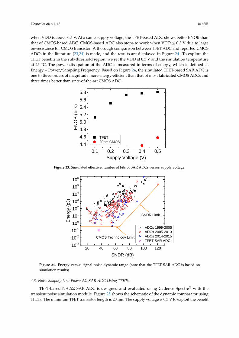
Electronics 2017, 6, 67 18 of 55
when VDD is above 0.5 V. At a same supply voltage, the TFET-based ADC shows better ENOB thanthat of CMOS-based ADC. CMOS-based ADC also stops to work when VDD ≤ 0.3 V due to largeon-resistance for CMOS transistor. A thorough comparison between TFET ADC and reported CMOSADCs in the literature [23,24] is made, and the results are displayed in Figure 24. To explore theTFET benefits in the sub-threshold region, we set the VDD at 0.3 V and the simulation temperatureat 25 ◦C. The power dissipation of the ADC is measured in terms of energy, which is defined asEnergy = Power/Sampling Frequency. Based on Figure 24, the simulated TFET-based SAR ADC isone to three orders of magnitude more energy-efficient than that of most fabricated CMOS ADCs andthree times better than state-of-the-art CMOS ADC.
Electronics 2017, 6, 67 18 of 54
that of CMOS‐based ADC. CMOS‐based ADC also stops to work when VDD ≤ 0.3 V due to large on‐
resistance for CMOS transistor. A thorough comparison between TFET ADC and reported CMOS
ADCs in the literature [23,24] is made, and the results are displayed in Figure 24. To explore the TFET
benefits in the sub‐threshold region, we set the VDD at 0.3 V and the simulation temperature at 25 °C.
The power dissipation of the ADC is measured in terms of energy, which is defined as Energy =
Power/Sampling Frequency. Based on Figure 24, the simulated TFET‐based SAR ADC is one to three
orders of magnitude more energy‐efficient than that of most fabricated CMOS ADCs and three times
better than state‐of‐the‐art CMOS ADC.
0.1 0.2 0.3 0.4 0.5
4.4
4.6
4.8
5.0
5.2
5.4
5.6
5.8
TFET 20nm CMOS
EN
OB
(bi
ts)
Supply Voltage (V)
Figure 23. Simulated effective number of bits of SAR ADCs versus supply voltage.
20 40 60 80 100 12010-3
10-2
10-1
100
101
102
103
104
105
106
ADCs 1999-2005 ADCs 2005-2013 ADCs 2014-2015 TFET SAR ADC
Ene
rgy
(pJ)
SNDR (dB)
CMOS Technology Limit
SNDR Limit
Figure 24. Energy versus signal noise dynamic range (note that the TFET SAR ADC is based on
simulation results).
4.3. Noise Shaping Low‐Power ΔƩ SAR ADC Using TFETs
TEFT‐based NS Δ� SAR ADC is designed and evaluated using Cadence Spectre® with the
transient noise simulation module. Figure 25 shows the schematic of the dynamic comparator using
TFETs. The minimum TFET transistor length is 20 nm. The supply voltage is 0.3 V to exploit the
benefit of near‐threshold operation. The temperature is at 25 °C. Under the normal condition, the
external clock frequency is 25 MHz.
Figure 23. Simulated effective number of bits of SAR ADCs versus supply voltage.
Electronics 2017, 6, 67 18 of 54
that of CMOS‐based ADC. CMOS‐based ADC also stops to work when VDD ≤ 0.3 V due to large on‐
resistance for CMOS transistor. A thorough comparison between TFET ADC and reported CMOS
ADCs in the literature [23,24] is made, and the results are displayed in Figure 24. To explore the TFET
benefits in the sub‐threshold region, we set the VDD at 0.3 V and the simulation temperature at 25 °C.
The power dissipation of the ADC is measured in terms of energy, which is defined as Energy =
Power/Sampling Frequency. Based on Figure 24, the simulated TFET‐based SAR ADC is one to three
orders of magnitude more energy‐efficient than that of most fabricated CMOS ADCs and three times
better than state‐of‐the‐art CMOS ADC.
0.1 0.2 0.3 0.4 0.5
4.4
4.6
4.8
5.0
5.2
5.4
5.6
5.8
TFET 20nm CMOS
EN
OB
(bi
ts)
Supply Voltage (V)
Figure 23. Simulated effective number of bits of SAR ADCs versus supply voltage.
20 40 60 80 100 12010-3
10-2
10-1
100
101
102
103
104
105
106
ADCs 1999-2005 ADCs 2005-2013 ADCs 2014-2015 TFET SAR ADC
Ene
rgy
(pJ)
SNDR (dB)
CMOS Technology Limit
SNDR Limit
Figure 24. Energy versus signal noise dynamic range (note that the TFET SAR ADC is based on
simulation results).
4.3. Noise Shaping Low‐Power ΔƩ SAR ADC Using TFETs
TEFT‐based NS Δ� SAR ADC is designed and evaluated using Cadence Spectre® with the
transient noise simulation module. Figure 25 shows the schematic of the dynamic comparator using
TFETs. The minimum TFET transistor length is 20 nm. The supply voltage is 0.3 V to exploit the
benefit of near‐threshold operation. The temperature is at 25 °C. Under the normal condition, the
external clock frequency is 25 MHz.
Figure 24. Energy versus signal noise dynamic range (note that the TFET SAR ADC is based onsimulation results).
4.3. Noise Shaping Low-Power ∆Σ SAR ADC Using TFETs
TEFT-based NS ∆Σ SAR ADC is designed and evaluated using Cadence Spectre® with thetransient noise simulation module. Figure 25 shows the schematic of the dynamic comparator usingTFETs. The minimum TFET transistor length is 20 nm. The supply voltage is 0.3 V to exploit the benefit
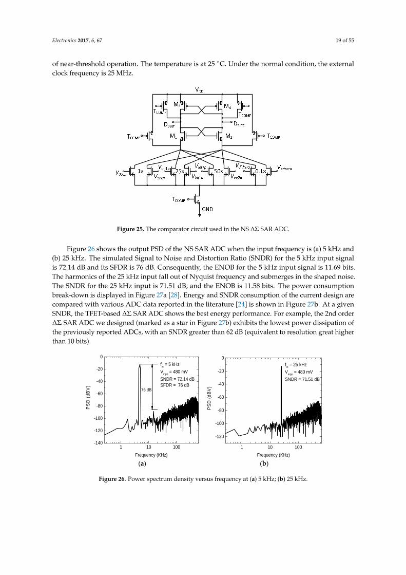
Electronics 2017, 6, 67 19 of 55
of near-threshold operation. The temperature is at 25 ◦C. Under the normal condition, the externalclock frequency is 25 MHz.Electronics 2017, 6, 67 19 of 54
Figure 25. The comparator circuit used in the NS ΔƩ SAR ADC.
Figure 26 shows the output PSD of the NS SAR ADC when the input frequency is (a) 5 kHz and
(b) 25 kHz. The simulated Signal to Noise and Distortion Ratio (SNDR) for the 5 kHz input signal is
72.14 dB and its SFDR is 76 dB. Consequently, the ENOB for the 5 kHz input signal is 11.69 bits. The
harmonics of the 25 kHz input fall out of Nyquist frequency and submerges in the shaped noise. The
SNDR for the 25 kHz input is 71.51 dB, and the ENOB is 11.58 bits. The power consumption break‐
down is displayed in Figure 27a [28]. Energy and SNDR consumption of the current design are
compared with various ADC data reported in the literature [24] is shown in Figure 27b. At a given
SNDR, the TFET‐based Δ� SAR ADC shows the best energy performance. For example, the 2nd order
Δ� SAR ADC we designed (marked as a star in Figure 27b) exhibits the lowest power dissipation of
the previously reported ADCs, with an SNDR greater than 62 dB (equivalent to resolution great
higher than 10 bits).
1 10 100-140
-120
-100
-80
-60
-40
-20
0
PS
D (
dBV
)
Frequency (KHz)
fin = 5 kHz
Vinpp
= 480 mV
SNDR = 72.14 dBSFDR = 76 dB
76 dB
1 10 100
-120
-100
-80
-60
-40
-20
0fin = 25 kHz
Vinpp
= 480 mV
SNDR = 71.51 dB
PS
D (
dBV
)
Frequency (KHz) (a) (b)
Figure 26. Power spectrum density versus frequency at (a) 5 kHz; (b) 25 kHz.
Figure 25. The comparator circuit used in the NS ∆Σ SAR ADC.
Figure 26 shows the output PSD of the NS SAR ADC when the input frequency is (a) 5 kHz and(b) 25 kHz. The simulated Signal to Noise and Distortion Ratio (SNDR) for the 5 kHz input signalis 72.14 dB and its SFDR is 76 dB. Consequently, the ENOB for the 5 kHz input signal is 11.69 bits.The harmonics of the 25 kHz input fall out of Nyquist frequency and submerges in the shaped noise.The SNDR for the 25 kHz input is 71.51 dB, and the ENOB is 11.58 bits. The power consumptionbreak-down is displayed in Figure 27a [28]. Energy and SNDR consumption of the current design arecompared with various ADC data reported in the literature [24] is shown in Figure 27b. At a givenSNDR, the TFET-based ∆Σ SAR ADC shows the best energy performance. For example, the 2nd order∆Σ SAR ADC we designed (marked as a star in Figure 27b) exhibits the lowest power dissipation ofthe previously reported ADCs, with an SNDR greater than 62 dB (equivalent to resolution great higherthan 10 bits).
Electronics 2017, 6, 67 19 of 54
Figure 25. The comparator circuit used in the NS ΔƩ SAR ADC.
Figure 26 shows the output PSD of the NS SAR ADC when the input frequency is (a) 5 kHz and
(b) 25 kHz. The simulated Signal to Noise and Distortion Ratio (SNDR) for the 5 kHz input signal is
72.14 dB and its SFDR is 76 dB. Consequently, the ENOB for the 5 kHz input signal is 11.69 bits. The
harmonics of the 25 kHz input fall out of Nyquist frequency and submerges in the shaped noise. The
SNDR for the 25 kHz input is 71.51 dB, and the ENOB is 11.58 bits. The power consumption break‐
down is displayed in Figure 27a [28]. Energy and SNDR consumption of the current design are
compared with various ADC data reported in the literature [24] is shown in Figure 27b. At a given
SNDR, the TFET‐based Δ� SAR ADC shows the best energy performance. For example, the 2nd order
Δ� SAR ADC we designed (marked as a star in Figure 27b) exhibits the lowest power dissipation of
the previously reported ADCs, with an SNDR greater than 62 dB (equivalent to resolution great
higher than 10 bits).
1 10 100-140
-120
-100
-80
-60
-40
-20
0
PS
D (
dBV
)
Frequency (KHz)
fin = 5 kHz
Vinpp
= 480 mV
SNDR = 72.14 dBSFDR = 76 dB
76 dB
1 10 100
-120
-100
-80
-60
-40
-20
0fin = 25 kHz
Vinpp
= 480 mV
SNDR = 71.51 dB
PS
D (
dBV
)
Frequency (KHz) (a) (b)
Figure 26. Power spectrum density versus frequency at (a) 5 kHz; (b) 25 kHz. Figure 26. Power spectrum density versus frequency at (a) 5 kHz; (b) 25 kHz.
Electronics 2017, 6, 67 20 of 55Electronics 2017, 6, 67 20 of 54
8%
4.5%
9.9%
77.6%
Switch-Capacitor Clock LFSR & SAR-Register Comparator
Total power = 0.94 W 20 40 60 80 100 12010-3
10-2
10-1
100
101
102
103
104
105
106
107
ADCs 1999-2005 ADCs 2005-2013 ADCs 2014-2015 TFET SAR ADC TFET SAR ADC
Ene
rgy
(pJ)
SNDR (dB)
CMOS Technology Limit
Noise Limit
(a) (b)
Figure 27. (a) Power distribution diagram; (b) Energy versus signal noise dynamic range.
4.4. Bio‐Inspired Ultra‐Low‐Power Computing
The human brain is the most efficient low‐power machine. A human brain contains about 1011
neurons and 1015 synapses to perform remarkable visual or other sensory perception tasks such as
classification, recognition, and cognitive reasoning. It handles immense amount of data for real‐time
processing and consumes approximately 20 W of power. Traditional von Neumann computing
systems based on CMOS technologies cannot achieve this level of energy efficiency. Neuromorphic
hardware systems that potentially provide the capabilities of biological perception and information
processing have gained much attention [75,76]. Bio‐inspired neuromorphic computing may open a
door to novel computation and communication paradigms. Figure 28 shows connectivity of
biological neurons and synapses for signal transmission in a neural network.
Figure 28. Schematic of biological neurons with synapses in a neural network.
Bio‐inspired computing may be used as the next‐generation ultra‐low‐power solution. A neuron
receives information from many synapses and adds the information together with different weights,
as represented in Figure 29a. When the summing signal reaches a firing threshold voltage in the
membrane, it produces an output spike. An integrate‐and‐fire (IF) neuron circuit schematic is show
in Figure 29b. Spiking neural networks (SNNs) are a prime candidate for enabling on‐chip
intelligence. Driven by brain‐like asynchronous event‐based computations, SNNs focus their
computational effort on currently active parts of the network, thereby achieving orders of lesser
power consumption compared to their artificial neural network (ANN) counterparts.
Figure 27. (a) Power distribution diagram; (b) Energy versus signal noise dynamic range.
4.4. Bio-Inspired Ultra-Low-Power Computing
The human brain is the most efficient low-power machine. A human brain contains about1011 neurons and 1015 synapses to perform remarkable visual or other sensory perception tasks such asclassification, recognition, and cognitive reasoning. It handles immense amount of data for real-timeprocessing and consumes approximately 20 W of power. Traditional von Neumann computing systemsbased on CMOS technologies cannot achieve this level of energy efficiency. Neuromorphic hardwaresystems that potentially provide the capabilities of biological perception and information processinghave gained much attention [75,76]. Bio-inspired neuromorphic computing may open a door to novelcomputation and communication paradigms. Figure 28 shows connectivity of biological neurons andsynapses for signal transmission in a neural network.
Electronics 2017, 6, 67 20 of 54
8%
4.5%
9.9%
77.6%
Switch-Capacitor Clock LFSR & SAR-Register Comparator
Total power = 0.94 W 20 40 60 80 100 12010-3
10-2
10-1
100
101
102
103
104
105
106
107
ADCs 1999-2005 ADCs 2005-2013 ADCs 2014-2015 TFET SAR ADC TFET SAR ADC
Ene
rgy
(pJ)
SNDR (dB)
CMOS Technology Limit
Noise Limit
(a) (b)
Figure 27. (a) Power distribution diagram; (b) Energy versus signal noise dynamic range.
4.4. Bio‐Inspired Ultra‐Low‐Power Computing
The human brain is the most efficient low‐power machine. A human brain contains about 1011
neurons and 1015 synapses to perform remarkable visual or other sensory perception tasks such as
classification, recognition, and cognitive reasoning. It handles immense amount of data for real‐time
processing and consumes approximately 20 W of power. Traditional von Neumann computing
systems based on CMOS technologies cannot achieve this level of energy efficiency. Neuromorphic
hardware systems that potentially provide the capabilities of biological perception and information
processing have gained much attention [75,76]. Bio‐inspired neuromorphic computing may open a
door to novel computation and communication paradigms. Figure 28 shows connectivity of
biological neurons and synapses for signal transmission in a neural network.
Figure 28. Schematic of biological neurons with synapses in a neural network.
Bio‐inspired computing may be used as the next‐generation ultra‐low‐power solution. A neuron
receives information from many synapses and adds the information together with different weights,
as represented in Figure 29a. When the summing signal reaches a firing threshold voltage in the
membrane, it produces an output spike. An integrate‐and‐fire (IF) neuron circuit schematic is show
in Figure 29b. Spiking neural networks (SNNs) are a prime candidate for enabling on‐chip
intelligence. Driven by brain‐like asynchronous event‐based computations, SNNs focus their
computational effort on currently active parts of the network, thereby achieving orders of lesser
power consumption compared to their artificial neural network (ANN) counterparts.
Figure 28. Schematic of biological neurons with synapses in a neural network.
Bio-inspired computing may be used as the next-generation ultra-low-power solution. A neuronreceives information from many synapses and adds the information together with different weights,as represented in Figure 29a. When the summing signal reaches a firing threshold voltage in themembrane, it produces an output spike. An integrate-and-fire (IF) neuron circuit schematic is show inFigure 29b. Spiking neural networks (SNNs) are a prime candidate for enabling on-chip intelligence.Driven by brain-like asynchronous event-based computations, SNNs focus their computational efforton currently active parts of the network, thereby achieving orders of lesser power consumptioncompared to their artificial neural network (ANN) counterparts.
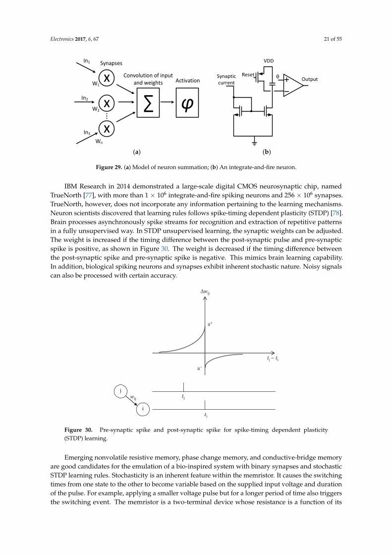
Electronics 2017, 6, 67 21 of 55Electronics 2017, 6, 67 21 of 54
x
x
x
∑ φ
Synapses
W1
W2
Wn
...
In1
In2
In3
Convolution of input and weights Activation
VDD
Synaptic current
Reset θ Output
(a) (b)
Figure 29. (a) Model of neuron summation; (b) An integrate‐and‐fire neuron.
IBM Research in 2014 demonstrated a large‐scale digital CMOS neurosynaptic chip, named
TrueNorth [77], with more than 1 × 10⁶ integrate‐and‐fire spiking neurons and 256 × 106 synapses.
TrueNorth, however, does not incorporate any information pertaining to the learning mechanisms.
Neuron scientists discovered that learning rules follows spike‐timing dependent plasticity (STDP)
[78]. Brain processes asynchronously spike streams for recognition and extraction of repetitive
patterns in a fully unsupervised way. In STDP unsupervised learning, the synaptic weights can be
adjusted. The weight is increased if the timing difference between the post‐synaptic pulse and pre‐
synaptic spike is positive, as shown in Figure 30. The weight is decreased if the timing difference
between the post‐synaptic spike and pre‐synaptic spike is negative. This mimics brain learning
capability. In addition, biological spiking neurons and synapses exhibit inherent stochastic nature.
Noisy signals can also be processed with certain accuracy.
Figure 30. Pre‐synaptic spike and post‐synaptic spike for spike‐timing dependent plasticity (STDP)
learning.
Emerging nonvolatile resistive memory, phase change memory, and conductive‐bridge memory
are good candidates for the emulation of a bio‐inspired system with binary synapses and stochastic
STDP learning rules. Stochasticity is an inherent feature within the memristor. It causes the switching
times from one state to the other to become variable based on the supplied input voltage and duration
of the pulse. For example, applying a smaller voltage pulse but for a longer period of time also
triggers the switching event. The memristor is a two‐terminal device whose resistance is a function
of its current state and input bias. It varies between a lower resistive state of RON and a higher resistive
state of ROFF similar to the RRAM performance described in Section 3.2.1. Innate variability of the
memristor switching between its two states is embraced to model stochastic binary synapses. A
Figure 29. (a) Model of neuron summation; (b) An integrate-and-fire neuron.
IBM Research in 2014 demonstrated a large-scale digital CMOS neurosynaptic chip, namedTrueNorth [77], with more than 1 × 10⁶ integrate-and-fire spiking neurons and 256 × 106 synapses.TrueNorth, however, does not incorporate any information pertaining to the learning mechanisms.Neuron scientists discovered that learning rules follows spike-timing dependent plasticity (STDP) [78].Brain processes asynchronously spike streams for recognition and extraction of repetitive patternsin a fully unsupervised way. In STDP unsupervised learning, the synaptic weights can be adjusted.The weight is increased if the timing difference between the post-synaptic pulse and pre-synapticspike is positive, as shown in Figure 30. The weight is decreased if the timing difference betweenthe post-synaptic spike and pre-synaptic spike is negative. This mimics brain learning capability.In addition, biological spiking neurons and synapses exhibit inherent stochastic nature. Noisy signalscan also be processed with certain accuracy.
Electronics 2017, 6, 67 21 of 54
x
x
x
∑ φ
Synapses
W1
W2
Wn
...
In1
In2
In3
Convolution of input and weights Activation
VDD
Synaptic current
Reset θ Output
(a) (b)
Figure 29. (a) Model of neuron summation; (b) An integrate‐and‐fire neuron.
IBM Research in 2014 demonstrated a large‐scale digital CMOS neurosynaptic chip, named
TrueNorth [77], with more than 1 × 10⁶ integrate‐and‐fire spiking neurons and 256 × 106 synapses.
TrueNorth, however, does not incorporate any information pertaining to the learning mechanisms.
Neuron scientists discovered that learning rules follows spike‐timing dependent plasticity (STDP)
[78]. Brain processes asynchronously spike streams for recognition and extraction of repetitive
patterns in a fully unsupervised way. In STDP unsupervised learning, the synaptic weights can be
adjusted. The weight is increased if the timing difference between the post‐synaptic pulse and pre‐
synaptic spike is positive, as shown in Figure 30. The weight is decreased if the timing difference
between the post‐synaptic spike and pre‐synaptic spike is negative. This mimics brain learning
capability. In addition, biological spiking neurons and synapses exhibit inherent stochastic nature.
Noisy signals can also be processed with certain accuracy.
Figure 30. Pre‐synaptic spike and post‐synaptic spike for spike‐timing dependent plasticity (STDP)
learning.
Emerging nonvolatile resistive memory, phase change memory, and conductive‐bridge memory
are good candidates for the emulation of a bio‐inspired system with binary synapses and stochastic
STDP learning rules. Stochasticity is an inherent feature within the memristor. It causes the switching
times from one state to the other to become variable based on the supplied input voltage and duration
of the pulse. For example, applying a smaller voltage pulse but for a longer period of time also
triggers the switching event. The memristor is a two‐terminal device whose resistance is a function
of its current state and input bias. It varies between a lower resistive state of RON and a higher resistive
state of ROFF similar to the RRAM performance described in Section 3.2.1. Innate variability of the
memristor switching between its two states is embraced to model stochastic binary synapses. A
Figure 30. Pre-synaptic spike and post-synaptic spike for spike-timing dependent plasticity(STDP) learning.
Emerging nonvolatile resistive memory, phase change memory, and conductive-bridge memoryare good candidates for the emulation of a bio-inspired system with binary synapses and stochasticSTDP learning rules. Stochasticity is an inherent feature within the memristor. It causes the switchingtimes from one state to the other to become variable based on the supplied input voltage and durationof the pulse. For example, applying a smaller voltage pulse but for a longer period of time also triggersthe switching event. The memristor is a two-terminal device whose resistance is a function of its
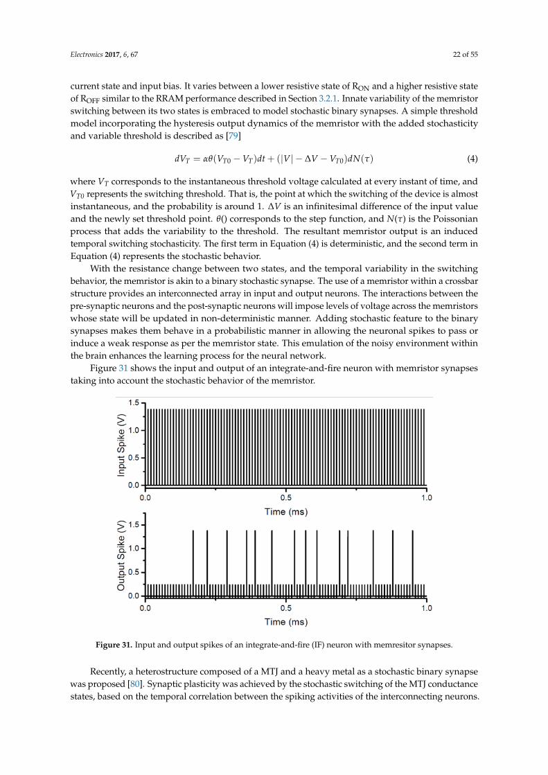
Electronics 2017, 6, 67 22 of 55
current state and input bias. It varies between a lower resistive state of RON and a higher resistive stateof ROFF similar to the RRAM performance described in Section 3.2.1. Innate variability of the memristorswitching between its two states is embraced to model stochastic binary synapses. A simple thresholdmodel incorporating the hysteresis output dynamics of the memristor with the added stochasticityand variable threshold is described as [79]
dVT = αθ(VT0 −VT)dt + (|V| − ∆V −VT0)dN(τ) (4)
where VT corresponds to the instantaneous threshold voltage calculated at every instant of time, andVT0 represents the switching threshold. That is, the point at which the switching of the device is almostinstantaneous, and the probability is around 1. ∆V is an infinitesimal difference of the input valueand the newly set threshold point. θ() corresponds to the step function, and N(τ) is the Poissonianprocess that adds the variability to the threshold. The resultant memristor output is an inducedtemporal switching stochasticity. The first term in Equation (4) is deterministic, and the second term inEquation (4) represents the stochastic behavior.
With the resistance change between two states, and the temporal variability in the switchingbehavior, the memristor is akin to a binary stochastic synapse. The use of a memristor within a crossbarstructure provides an interconnected array in input and output neurons. The interactions between thepre-synaptic neurons and the post-synaptic neurons will impose levels of voltage across the memristorswhose state will be updated in non-deterministic manner. Adding stochastic feature to the binarysynapses makes them behave in a probabilistic manner in allowing the neuronal spikes to pass orinduce a weak response as per the memristor state. This emulation of the noisy environment withinthe brain enhances the learning process for the neural network.
Figure 31 shows the input and output of an integrate-and-fire neuron with memristor synapsestaking into account the stochastic behavior of the memristor.
Electronics 2017, 6, 67 22 of 54
simple threshold model incorporating the hysteresis output dynamics of the memristor with the
added stochasticity and variable threshold is described as [79]
)()()( 00 dNVVVdtVVdV TTTT (4)
where VT corresponds to the instantaneous threshold voltage calculated at every instant of time, and
VT0 represents the switching threshold. That is, the point at which the switching of the device is almost
instantaneous, and the probability is around 1. ∆V is an infinitesimal difference of the input value
and the newly set threshold point. θ() corresponds to the step function, and N(τ) is the Poissonian
process that adds the variability to the threshold. The resultant memristor output is an induced
temporal switching stochasticity. The first term in Equation (4) is deterministic, and the second term
in Equation (4) represents the stochastic behavior.
With the resistance change between two states, and the temporal variability in the switching
behavior, the memristor is akin to a binary stochastic synapse. The use of a memristor within a
crossbar structure provides an interconnected array in input and output neurons. The interactions
between the pre‐synaptic neurons and the post‐synaptic neurons will impose levels of voltage across
the memristors whose state will be updated in non‐deterministic manner. Adding stochastic feature
to the binary synapses makes them behave in a probabilistic manner in allowing the neuronal spikes
to pass or induce a weak response as per the memristor state. This emulation of the noisy
environment within the brain enhances the learning process for the neural network.
Figure 31 shows the input and output of an integrate‐and‐fire neuron with memristor synapses
taking into account the stochastic behavior of the memristor.
Figure 31. Input and output spikes of an integrate‐and‐fire (IF) neuron with memresitor synapses.
Recently, a heterostructure composed of a MTJ and a heavy metal as a stochastic binary synapse
was proposed [80]. Synaptic plasticity was achieved by the stochastic switching of the MTJ
conductance states, based on the temporal correlation between the spiking activities of the
interconnecting neurons. The efficacy of the proposed synaptic configurations and the stochastic
learning algorithm on an SNN trained to classify handwritten digits from a MNIST dataset was
demonstrated. The power efficiency of the proposed neuromorphic system stems from the ultra‐low
programming energy of the spintronic synapses.
Figure 31. Input and output spikes of an integrate-and-fire (IF) neuron with memresitor synapses.
Recently, a heterostructure composed of a MTJ and a heavy metal as a stochastic binary synapsewas proposed [80]. Synaptic plasticity was achieved by the stochastic switching of the MTJ conductancestates, based on the temporal correlation between the spiking activities of the interconnecting neurons.
Electronics 2017, 6, 67 23 of 55
The efficacy of the proposed synaptic configurations and the stochastic learning algorithm on anSNN trained to classify handwritten digits from a MNIST dataset was demonstrated. The powerefficiency of the proposed neuromorphic system stems from the ultra-low programming energy of thespintronic synapses.
5. Hardware Security
IoT connectivity with embedded sensors, processors, and actuators that sense and interact withthe physical world at any time and any place creates security and privacy challenges. IoT devices arevenerable to hacking. For example, the Google Nest thermostat used in a smart home can be hackedby accessing the sys_boot pin in the Nest Thermostat [81]. The processing unit will start operatingbased on the incoming instructions from either the USB or the UART3 port once sys_boot is withdrawnsignificantly. The adversary might exploit this boot vulnerability to insert his or her own codes intothe device. A vulnerable IoT device could be used to attack other components or devices that are onthe same IoT network. The goal of such attacks is to leak private or unauthorized data for end-usersthough using backdoor insertion.
5.1. Encryption
Encryption is defined as one of the most widespread techniques that is utilized to protect thetransceiving data from unauthorized users, snooping attacks. Several encryption methodologieshave been proposed, but the more robust one is the Advanced Encryption Standard (AES) [82].Implementing AES on a chip is very important in the IoT system. However, the hardwareimplementation of an AES algorithm is more complex compared to other encryption algorithms.Moreover, many side channel attacks have been demonstrated to recover the secret key using theaccelerated algorithm [83]. The complexity of AES could be mitigated though partitioning thealgorithm into segments, such as Shift row, S-box, and Mix column. For example, implementingAES encryption with 128 bit plaintext (4 × 4 array, namely state machine (SM)) can mainly be achievedin four steps, where the number of required rounds depends on the length of the encrypted key-bits.Each AES round includes four operations: SubBytes, ShiftRows, MixColimns, and AddRoundKey.SubBytes: Each incoming 16 bytes converts to a different value though a simple substitution operationusing an S-box function, where a table with 256 values are introduced for substitution purposes.ShiftRows: This operation performs on each row of the state array, in which each row is rotated to theleft via a specific number of bytes. This step is used to scramble the 128-bit data block. MixColimns:This operation is used to create a new column by multiplying each state array column by a matrixhaving 1, 2, and 3 numbers, where the new columns are exchanged with the one. The MixColimnstransformation could be implemented using XOR with NAND logic gates (to perform shift and addoperations). AddRoundKey: The last step is XORed the secret round key. Based on the aforementioneddiscussion, AES requires several XOR gates and shift operations, which could offer good advantageswith certain technologies that provide low overhead on implementing XOR and shift operations.
Rivest, Shamir, and Adleman (RSA) [84] introduced a cryptographic algorithm for improvedsecurity. RSA is a public-key cryptosystem. The encryption and decryption operations of an RSAalgorithm are achieved using two different keys, namely a public key and a private key, where thepublic key is used to encrypt the plaintext and the private key is utilized to recover (decrypt) thedata at the receiver. The difficulty of implementing RSA cryptography is to produce the public andthe private keys since these keys should be large prime numbers. Otherwise, it will be vulnerable tobrute force attacks. Another kind of asymmetric key cryptography, called Elliptic Curve Cryptography(ECC), has been developed [85]. ECC provides good security with lower computation cost. ECC issuitable in many applications, such as healthcare systems, and wireless and mobile environments.ECC provides high-level security, which is similar to RSA cryptography, with a smaller key size.As a consequence, it will provide superior performance, cost less, and reduce power dissipation.Gura et al. [86] compared ECC and RSA performance using 8-bit microcontrollers. They were able to
Electronics 2017, 6, 67 24 of 55
achieve a 1024-bit RSA private key operation with exponent e = 1016 + 1 in 0.43 s and 160-bit ellipticcurrent point multiplication in 0.81 s with a clock speed of 8 MHz on the 8-bit microcontroller.
Even though AES and RSA encryption cryptographies can offer a high security level, they arenot suitable for an application that requires a small area and low power dissipation, such as IoTsystems. A lightweight encryption algorithm is more suitable for IoT applications since it requires asmaller area and lower power compared to AES and RSA encryption techniques. This is due to thefact that block size of the lightweight encryption cryptography is smaller than 64 bits, while the blocksize in AES is larger than 128 bits. For instance, both lightweight Data Encryption Standards (DES),DESXL and DESL, are proposed in [87]. The round function in DES can be replaced by S-box becausea DES algorithm depends on the derivative data. This eliminates the need of the initial and finalpermutations. To further reduce the complexity of the encryption cryptography, two other encryptioncryptographies, namely KATAN and KTANTAN, were introduced in 2009 [88]. KATAN/KTANTANis a family of hardware-oriented block ciphers designed by Chrstophe de Canniere, Orr Dunkelman,and Miroslav Knezevic. The lightweight KATAN design consists of 256 rounds, shift registers, andnonlinear feedback functions. Each cipher has three different block sizes, 32 bits, 48 bits, and 64 bits,with 80 bit symmetric key size. The block of the KATAN cipher iterates for 256 rounds to produce theencrypted output data (ciphertext), where the key schedule with an 80 bit key size is shared with allKATAN blocks. Since the difference among the three cipher blocks regarding the required hardwareresources is only the size of the register, we concentrate on the 32 bit blocks of the KATAN cipher.The 32-bit blocks is organized in 32 registers. The first 13 registers are located in the L1 part and theremaining 19 registers are in the L2 part. L1 and L2 blocks operate as a linear feedback shift register(LFSR). At each clock cycle, the data in both L1 and L2 blocks are shifted. L1 and L2 are used in boththe encryption and decryption sides. For the encryption purposes, the plaintext is stored in both L1and L2 blocks, where L1 carries the first 19 bits and L1 carries the remaining 13 bits of the plaintext.The computation of the two nonlinear functions, called fa(L1) and fb(L2), which consist of several XORand AND operations, is achieved on data coming from the non-linear irregular factor (IR), differentlocations in L1 (at fb) and L2 (fa), and different key-bits, namely Ka and Kb.
Figure 32 shows both the least significant bits (LSBs) and the most significant bits (MSBs) for eachL1 and L2 registers. For each clock cycle, the data in both L1 and L2 are shifted. Ka and Kb keys withIR are produced from two other blocks at each round. Figure 33a demonstrates the IR block, whichcontains 8 bit LFSR. Two operations are done in this block: first, counting the number of the rounds,and generating the irregular new value for the two function (fa and fb). The encryption process iscomplete once the number of rounds reaches 254 cycles. Another important block of the key scheduleis shown in Figure 33b. This register has 80 bit LFSR, where the value of the secret key is loaded to thisblock before the encryption is started. Each round key is generated by shifting one bit in the LFSRgenerator. The two keys (Ka and Kb) are produced from the last two significant bits every two cycles.Equation (5) shows the reciprocal polynomial of the LFSR generator with 4 taps located at 13th, 50th,60th, and 80th bits, which are chosen for the 80 bit shift register. The definition of the key, which isreferred to K, and the buskey of round j is presented in Equation (6).
f (x) = x80 + x61 + x50 + x13 + 1 (5)
k j =
{Kj j = 0 . . . 79k j−80 ⊕ k j−61 ⊕ k j−50 ⊕ k j−13 j > 79
(6)
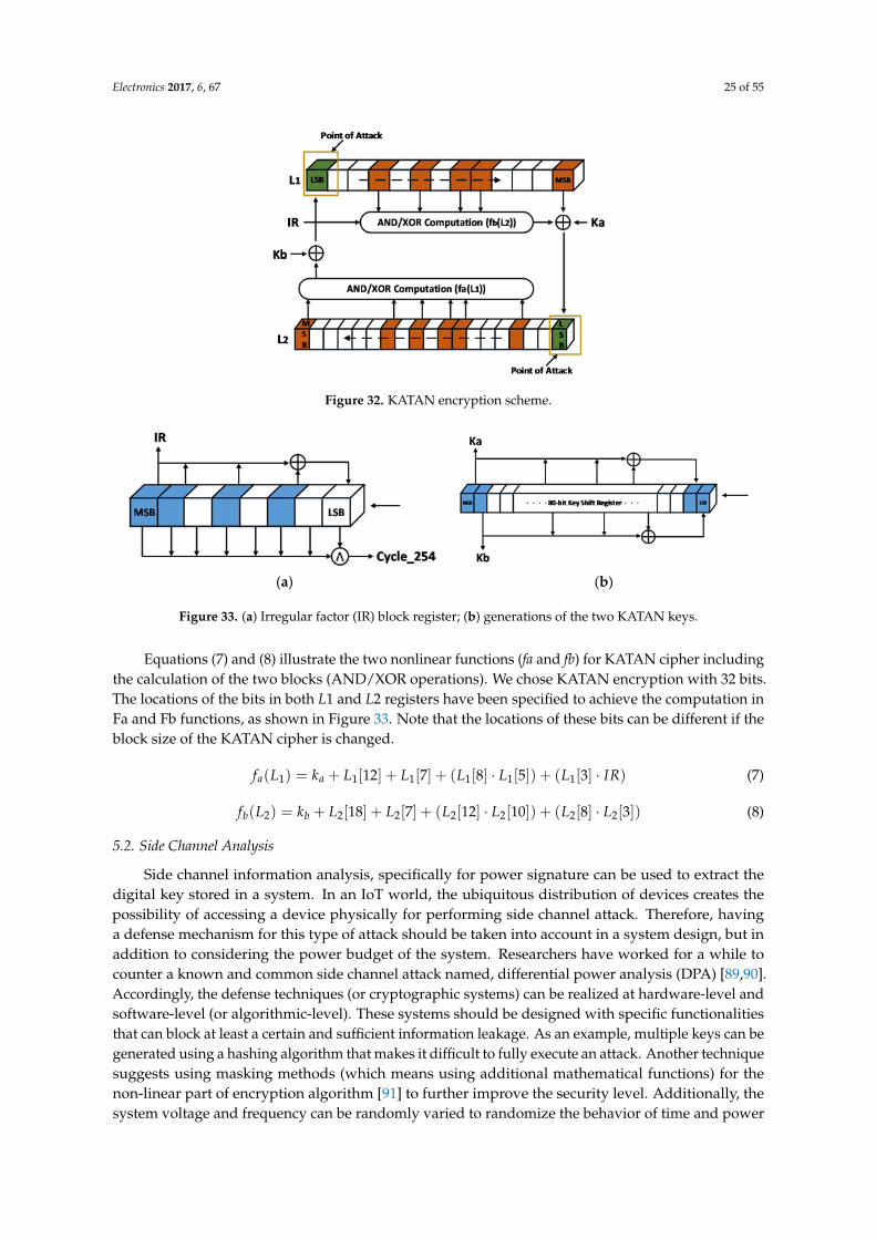
Electronics 2017, 6, 67 25 of 55
Electronics 2017, 6, 67 24 of 54
fact that block size of the lightweight encryption cryptography is smaller than 64 bits, while the block
size in AES is larger than 128 bits. For instance, both lightweight Data Encryption Standards (DES),
DESXL and DESL, are proposed in [87]. The round function in DES can be replaced by S‐box because
a DES algorithm depends on the derivative data. This eliminates the need of the initial and final
permutations. To further reduce the complexity of the encryption cryptography, two other
encryption cryptographies, namely KATAN and KTANTAN, were introduced in 2009 [88].
KATAN/KTANTAN is a family of hardware‐oriented block ciphers designed by Chrstophe de
Canniere, Orr Dunkelman, and Miroslav Knezevic. The lightweight KATAN design consists of 256
rounds, shift registers, and nonlinear feedback functions. Each cipher has three different block sizes,
32 bits, 48 bits, and 64 bits, with 80 bit symmetric key size. The block of the KATAN cipher iterates
for 256 rounds to produce the encrypted output data (ciphertext), where the key schedule with an 80
bit key size is shared with all KATAN blocks. Since the difference among the three cipher blocks
regarding the required hardware resources is only the size of the register, we concentrate on the 32
bit blocks of the KATAN cipher. The 32‐bit blocks is organized in 32 registers. The first 13 registers
are located in the L1 part and the remaining 19 registers are in the L2 part. L1 and L2 blocks operate
as a linear feedback shift register (LFSR). At each clock cycle, the data in both L1 and L2 blocks are
shifted. L1 and L2 are used in both the encryption and decryption sides. For the encryption purposes,
the plaintext is stored in both L1 and L2 blocks, where L1 carries the first 19 bits and L1 carries the
remaining 13 bits of the plaintext. The computation of the two nonlinear functions, called fa(L1) and
fb(L2), which consist of several XOR and AND operations, is achieved on data coming from the non‐
linear irregular factor (IR), different locations in L1 (at fb) and L2 (fa), and different key‐bits, namely
Ka and Kb.
Figure 32 shows both the least significant bits (LSBs) and the most significant bits (MSBs) for
each L1 and L2 registers. For each clock cycle, the data in both L1 and L2 are shifted. Ka and Kb keys
with IR are produced from two other blocks at each round. Figure 33a demonstrates the IR block,
which contains 8 bit LFSR. Two operations are done in this block: first, counting the number of the
rounds, and generating the irregular new value for the two function (fa and fb). The encryption
process is complete once the number of rounds reaches 254 cycles. Another important block of the
key schedule is shown in Figure 33b. This register has 80 bit LFSR, where the value of the secret key
is loaded to this block before the encryption is started. Each round key is generated by shifting one
bit in the LFSR generator. The two keys (Ka and Kb) are produced from the last two significant bits
every two cycles. Equation (5) shows the reciprocal polynomial of the LFSR generator with 4 taps
located at 13th, 50th, 60th, and 80th bits, which are chosen for the 80 bit shift register. The definition
of the key, which is referred to K, and the buskey of round j is presented in Equation (6).
Figure 32. KATAN encryption scheme. Figure 32. KATAN encryption scheme.Electronics 2017, 6, 67 25 of 54
(a) (b)
Figure 33. (a) Irregular factor (IR) block register; (b) generations of the two KATAN keys.
1)( 13506180 xxxxxf
(5)
79
79...0
13506180 jkkkk
jKk
jjjj
j
j (6)
Equations (7) and (8) illustrate the two nonlinear functions (fa and fb) for KATAN cipher
including the calculation of the two blocks (AND/XOR operations). We chose KATAN encryption
with 32 bits. The locations of the bits in both L1 and L2 registers have been specified to achieve the
computation in Fa and Fb functions, as shown in Figure 33. Note that the locations of these bits can
be different if the block size of the KATAN cipher is changed.
)]3[(])5[]8[(]7[]12[)( 111111 IRLLLLLkLf aa (7)
])3[]8[(])10[]12[(]7[]18[)( 2222222 LLLLLLkLf bb (8)
5.2. Side Channel Analysis
Side channel information analysis, specifically for power signature can be used to extract the
digital key stored in a system. In an IoT world, the ubiquitous distribution of devices creates the
possibility of accessing a device physically for performing side channel attack. Therefore, having a
defense mechanism for this type of attack should be taken into account in a system design, but in
addition to considering the power budget of the system. Researchers have worked for a while to
counter a known and common side channel attack named, differential power analysis (DPA) [89,90].
Accordingly, the defense techniques (or cryptographic systems) can be realized at hardware‐level
and software‐level (or algorithmic‐level). These systems should be designed with specific
functionalities that can block at least a certain and sufficient information leakage. As an example,
multiple keys can be generated using a hashing algorithm that makes it difficult to fully execute an
attack. Another technique suggests using masking methods (which means using additional
mathematical functions) for the non‐linear part of encryption algorithm [91] to further improve the
security level. Additionally, the system voltage and frequency can be randomly varied to randomize
the behavior of time and power traces, so as to prevent side‐channel attacks at the gate‐level. Yang et
al. [92] proposed the employment of sense amplifier‐based logic style for cryptographic algorithm
implementations that makes power consumption independent (or irrelevant) of the processed data.
Similarly, a traditional circuit level protection scheme is current mode logic (CML), a traditional
circuit level protection scheme that provides both power efficiency and security enhancement. In
order to evaluate a systemʹs security, we cannot solely focus on the differential power analysis; other
attacking schemes such as correlation power analysis should be considered.
Differential power analysis and correlation power analysis will now be discussed. Performing
correlation power analysis on the KATAN cryptographic system [93] has been studied. According to
[94], the intermediate values in computations of a cryptographic system during differential power
Figure 33. (a) Irregular factor (IR) block register; (b) generations of the two KATAN keys.
Equations (7) and (8) illustrate the two nonlinear functions (fa and fb) for KATAN cipher includingthe calculation of the two blocks (AND/XOR operations). We chose KATAN encryption with 32 bits.The locations of the bits in both L1 and L2 registers have been specified to achieve the computation inFa and Fb functions, as shown in Figure 33. Note that the locations of these bits can be different if theblock size of the KATAN cipher is changed.
fa(L1) = ka + L1[12] + L1[7] + (L1[8] · L1[5]) + (L1[3] · IR) (7)
fb(L2) = kb + L2[18] + L2[7] + (L2[12] · L2[10]) + (L2[8] · L2[3]) (8)
5.2. Side Channel Analysis
Side channel information analysis, specifically for power signature can be used to extract thedigital key stored in a system. In an IoT world, the ubiquitous distribution of devices creates thepossibility of accessing a device physically for performing side channel attack. Therefore, havinga defense mechanism for this type of attack should be taken into account in a system design, but inaddition to considering the power budget of the system. Researchers have worked for a while tocounter a known and common side channel attack named, differential power analysis (DPA) [89,90].Accordingly, the defense techniques (or cryptographic systems) can be realized at hardware-level andsoftware-level (or algorithmic-level). These systems should be designed with specific functionalitiesthat can block at least a certain and sufficient information leakage. As an example, multiple keys can begenerated using a hashing algorithm that makes it difficult to fully execute an attack. Another techniquesuggests using masking methods (which means using additional mathematical functions) for thenon-linear part of encryption algorithm [91] to further improve the security level. Additionally, thesystem voltage and frequency can be randomly varied to randomize the behavior of time and power
Electronics 2017, 6, 67 26 of 55
traces, so as to prevent side-channel attacks at the gate-level. Yang et al. [92] proposed the employmentof sense amplifier-based logic style for cryptographic algorithm implementations that makes powerconsumption independent (or irrelevant) of the processed data. Similarly, a traditional circuit levelprotection scheme is current mode logic (CML), a traditional circuit level protection scheme thatprovides both power efficiency and security enhancement. In order to evaluate a system’s security,we cannot solely focus on the differential power analysis; other attacking schemes such as correlationpower analysis should be considered.
Differential power analysis and correlation power analysis will now be discussed. Performingcorrelation power analysis on the KATAN cryptographic system [93] has been studied. Accordingto [94], the intermediate values in computations of a cryptographic system during differential poweranalysis must be extracted and identified. These values along with the plaintext and ciphertext help todiscover the keys. A smaller size of round keys (or intermediate keys) results in fewer computations ofthe DPA and consequently an easier system key analysis and discovery. Besides acquiring the actualpower traces from the system, a number of key guesses are used to calculate the intermediate valuesthat are considered hypothetical power traces. Next, the actual and hypothetical power traces areclassified by a selection function, and analysis of the function outcome reveals a peak for the correctkey hypothesis. An extension of the DPA in which a power model is used along with the intermediatevalues for computation of the hypothetical power traces is called correlation power analysis (CPA).The actual power and the predicted power traces are input into a correlation function to find thehighest correlation value that is perhaps corresponding to the correctly guessed key. The leveragedpower model in the CPA is the Hamming weight model; in the DPA, it is Hamming distance model.
The authors of [93] proposed a security evaluation of the KATAN family of cryptographic systemsby analyzing the algebraic and the cube attacks. Additionally, the possibility of attacking a KATANsystem by side channel analysis was mentioned. According to the KATAN algorithm, the plaintext andthe ciphertext are related to the intermediate keys through two nonlinear functions that are “fa” and“fb”. Next, the output bits of these two functions are the intermediate values or the targeting points ofthe attack. These two points can be seen in Figure 32. The hardware implementation of the KATANcryptographic algorithm mainly consists of D flip flops. Thus, the overall power consumption of thesystem is largely dependent on these elements. As a consequence, an attack model that maximizes thecontributions of the nonlinear functions to the system power traces must be utilized. The maximizationcan occur (in static logic style) by constructing the plaintext based on the convention of having a logicalone-to-zero or zero-to-one transition at the one-function output bits for certain clock cycles, whichcauses a closer relationship between the power traces and the key. In this way, each portion of the keyis revealed in every clock cycle until the whole key is extracted.
5.3. Supply Chain Security
Protecting electronic circuits and systems from counterfeiting IC in the supply chain is a concern.In general, attackers usually use cheap and simple methodologies in order to counterfeit or illegallycopy chips. The produced chips might be unreliable and not work properly due to counterfeiting.Such counterfeited ICs may fail the system and consequently could put human beings’ life in danger.The program of the Supply Chain Integrity for Electronics Defense (SHIELD) has been supported by theDefense Advanced Research Projects Agency (DARPA) in the United States to prevent counterfeitingand protect ICs via increasing the complexity of the design, which leads to a significant increasein the cost. In this case, the packaging of ICs consists of an encryption technique, e.g., NationalSecurity Agency (NSA) encryption, near-field communications, and sensors [95]. The occupied areafor the trustworthy hardware will be approximately 100 × 100 µm2 (dielet), which is important forprohibiting attackers from accessing or reverse-engineering the dielet. ICs can be authenticated byusing physical devices, called external probes, which will give an inductive/RF near-field readerthat powers the dielet for a period long enough to exchange information that allows the dielet toidentify and authenticate itself and provide an update of its passive environmental sensor readings.
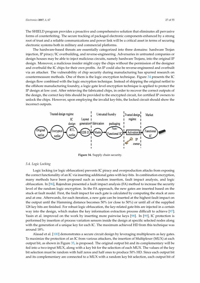
Electronics 2017, 6, 67 27 of 55
The SHIELD program provides a proactive and comprehensive solution that eliminates all pervasiveforms of counterfeiting. The secure tracking of packaged electronic components enhanced by a strongroot of trust and a reliable communications and power link will be a critical asset in terms of securingelectronic systems both in military and commercial platforms.
The hardware-based threats are essentially categorized into three domains: hardware Trojaninjection, IP piracy/IC overbuilding, and reverse-engineering. Adversaries in untrusted companies ordesign houses may be able to inject malicious circuits, namely hardware Trojans, into the original IPdesign. Moreover, a malicious insider might copy the chips without the permission of the designerand overbuild the IC chips for their own profits. An IP could also be reverse-engineered and overbuiltvia an attacker. The vulnerability of chip security during manufacturing has spurred research oncountermeasure methods. One of them is the logic encryption technique. Figure 34 presents the ICdesign flow combined with the logic encryption technique. Instead of shipping the original netlist tothe offshore manufacturing foundry, a logic-gate level encryption technique is applied to protect theIP design at low cost. After retrieving the fabricated chips, in order to recover the correct outputs ofthe design, the correct key-bits should be provided to the encrypted circuit, for certified IP owners tounlock the chips. However, upon employing the invalid key-bits, the locked circuit should show theincorrect outputs.
Electronics 2017, 6, 67 27 of 54
countermeasure methods. One of them is the logic encryption technique. Figure 34 presents the IC
design flow combined with the logic encryption technique. Instead of shipping the original netlist to
the offshore manufacturing foundry, a logic‐gate level encryption technique is applied to protect the
IP design at low cost. After retrieving the fabricated chips, in order to recover the correct outputs of
the design, the correct key‐bits should be provided to the encrypted circuit, for certified IP owners to
unlock the chips. However, upon employing the invalid key‐bits, the locked circuit should show the
incorrect outputs.
Figure 34. Supply chain security.
5.4. Logic Locking
Logic locking (or logic obfuscation) prevents IC piracy and overproduction attacks from
exposing the correct functionality of an IC via inserting additional gates with key‐bits. In combination
encryption, many methods have been proposed such as random insertion, fault impact analysis, and
logic obfuscation. In [96], Rajendran presented a fault impact analysis (FA) method to increase the
security level of the random logic encryption. In the FA approach, the new gates are inserted based
on the stuck‐at fault model. First, the fault impact for each gate is calculated by computing the stuck
at zero and at one. Afterwards, for each iteration, a new gate can be inserted at the highest fault
impact on the output until the Hamming distance becomes 50% (or close to 50%) or until all of the
supplied 128 key bits are finished. For robust logic obfuscation, the key‐related gate‐bits are injected
in a certain way into the design, which makes the key information extraction process difficult to
achieve [97]. Yasin et al. improved on the work by inserting more pairwise keys [98]. In [99], IC
protection is performed by insertion of process variation sensors inside the design at specific selected
nodes along with the generation of a unique key for each IC. The maximum achieved HD from this
technique was around 18%.
Alasad et al. [100] demonstrates a secure circuit design by leveraging multiplexers as key gates.
To maximize the protection of an IC from various attackers, the insertion of Multiplexer (MUX) at
each output bit, as shown in Figure 35, is proposed. The original output bit and its complementary
will be fed into a two‐input MUX, along with a key bit for the selection of each MUX. The values of
the key bit selection must be random with half zeros and half ones to produce 50% HD. Since each
output bit and its complementary are connected to a MUX with a random key bit selection, each
output bit of the IC is changeable once the key is changed. In this case, not only is the HD between
the corrected and corrupted outputs around 50%, but the value of each output bit is also variable. An
assailant cannot figure out the functionality of the design because each output bit will vary according
to the supplied key via the LFSR generator, which is used to generate random keys (each key is
generated to have randomly half zeros and half ones, as mentioned). Since the key value is
unpredictable due to the random generation, each output bit will be consequently arbitrary. Once the
correct user key is inserted, the output of the payload will be set, and the enable (EN) of the LFSR
generator will then be disabled, while the activation signal (A) will be activated to initialize the values
of the MUX selections. Then, the functionality of the circuit will be correct. If the value of one bit in
the user key is incorrect, the corrupted output ratio will still be around 50%. Although inserting MUX
at each output bit will obviously maximize the protection of the design, as well as the ambiguity of
an attacker, the power and area overheads will largely increase. Therefore, this technique is more
Figure 34. Supply chain security.
5.4. Logic Locking
Logic locking (or logic obfuscation) prevents IC piracy and overproduction attacks from exposingthe correct functionality of an IC via inserting additional gates with key-bits. In combination encryption,many methods have been proposed such as random insertion, fault impact analysis, and logicobfuscation. In [96], Rajendran presented a fault impact analysis (FA) method to increase the securitylevel of the random logic encryption. In the FA approach, the new gates are inserted based on thestuck-at fault model. First, the fault impact for each gate is calculated by computing the stuck at zeroand at one. Afterwards, for each iteration, a new gate can be inserted at the highest fault impact onthe output until the Hamming distance becomes 50% (or close to 50%) or until all of the supplied128 key bits are finished. For robust logic obfuscation, the key-related gate-bits are injected in a certainway into the design, which makes the key information extraction process difficult to achieve [97].Yasin et al. improved on the work by inserting more pairwise keys [98]. In [99], IC protection isperformed by insertion of process variation sensors inside the design at specific selected nodes alongwith the generation of a unique key for each IC. The maximum achieved HD from this technique wasaround 18%.
Alasad et al. [100] demonstrates a secure circuit design by leveraging multiplexers as key gates.To maximize the protection of an IC from various attackers, the insertion of Multiplexer (MUX) at eachoutput bit, as shown in Figure 35, is proposed. The original output bit and its complementary will befed into a two-input MUX, along with a key bit for the selection of each MUX. The values of the keybit selection must be random with half zeros and half ones to produce 50% HD. Since each output bitand its complementary are connected to a MUX with a random key bit selection, each output bit of
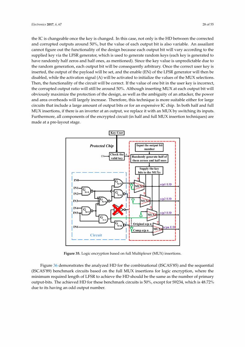
Electronics 2017, 6, 67 28 of 55
the IC is changeable once the key is changed. In this case, not only is the HD between the correctedand corrupted outputs around 50%, but the value of each output bit is also variable. An assailantcannot figure out the functionality of the design because each output bit will vary according to thesupplied key via the LFSR generator, which is used to generate random keys (each key is generated tohave randomly half zeros and half ones, as mentioned). Since the key value is unpredictable due tothe random generation, each output bit will be consequently arbitrary. Once the correct user key isinserted, the output of the payload will be set, and the enable (EN) of the LFSR generator will then bedisabled, while the activation signal (A) will be activated to initialize the values of the MUX selections.Then, the functionality of the circuit will be correct. If the value of one bit in the user key is incorrect,the corrupted output ratio will still be around 50%. Although inserting MUX at each output bit willobviously maximize the protection of the design, as well as the ambiguity of an attacker, the powerand area overheads will largely increase. Therefore, this technique is more suitable either for largecircuits that include a large amount of output bits or for an expensive IC chip. In both half and fullMUX insertions, if there is an inverter at an output, we replace it with an MUX by switching its inputs.Furthermore, all components of the encrypted circuit (in half and full MUX insertion techniques) aremade at a pre-layout stage.
Electronics 2017, 6, 67 28 of 54
suitable either for large circuits that include a large amount of output bits or for an expensive IC chip.
In both half and full MUX insertions, if there is an inverter at an output, we replace it with an MUX
by switching its inputs. Furthermore, all components of the encrypted circuit (in half and full MUX
insertion techniques) are made at a pre‐layout stage.
Figure 35. Logic encryption based on full Multiplexer (MUX) insertions.
Figure 36 demonstrates the analyzed HD for the combinational (ISCAS’85) and the sequential
(ISCAS’89) benchmark circuits based on the full MUX insertions for logic encryption, where the
minimum required length of LFSR to achieve the HD should be the same as the number of primary
output‐bits. The achieved HD for these benchmark circuits is 50%, except for S9234, which is 48.72%
due to its having an odd output number.
Figure 36. MUX insertions based on the full output number for different ISCAS ‘85 and ‘89 benchmark circuits.
The delay, power, and area overhead for each benchmark circuit is measured using the design
compiler tools from Synopsys with a 45 nm CMOS library. Since MUXs were inserted only at the
output of the netlist, the delay overhead (timing path) is almost zero for all of the benchmark circuits.
Figure 35. Logic encryption based on full Multiplexer (MUX) insertions.
Figure 36 demonstrates the analyzed HD for the combinational (ISCAS’85) and the sequential(ISCAS’89) benchmark circuits based on the full MUX insertions for logic encryption, where theminimum required length of LFSR to achieve the HD should be the same as the number of primaryoutput-bits. The achieved HD for these benchmark circuits is 50%, except for S9234, which is 48.72%due to its having an odd output number.
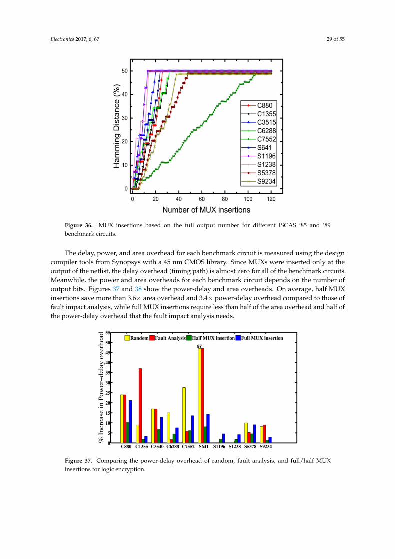
Electronics 2017, 6, 67 29 of 55
Electronics 2017, 6, 67 28 of 54
suitable either for large circuits that include a large amount of output bits or for an expensive IC chip.
In both half and full MUX insertions, if there is an inverter at an output, we replace it with an MUX
by switching its inputs. Furthermore, all components of the encrypted circuit (in half and full MUX
insertion techniques) are made at a pre‐layout stage.
Figure 35. Logic encryption based on full Multiplexer (MUX) insertions.
Figure 36 demonstrates the analyzed HD for the combinational (ISCAS’85) and the sequential
(ISCAS’89) benchmark circuits based on the full MUX insertions for logic encryption, where the
minimum required length of LFSR to achieve the HD should be the same as the number of primary
output‐bits. The achieved HD for these benchmark circuits is 50%, except for S9234, which is 48.72%
due to its having an odd output number.
Figure 36. MUX insertions based on the full output number for different ISCAS ‘85 and ‘89 benchmark circuits.
The delay, power, and area overhead for each benchmark circuit is measured using the design
compiler tools from Synopsys with a 45 nm CMOS library. Since MUXs were inserted only at the
output of the netlist, the delay overhead (timing path) is almost zero for all of the benchmark circuits.
Figure 36. MUX insertions based on the full output number for different ISCAS ’85 and ’89benchmark circuits.
The delay, power, and area overhead for each benchmark circuit is measured using the designcompiler tools from Synopsys with a 45 nm CMOS library. Since MUXs were inserted only at theoutput of the netlist, the delay overhead (timing path) is almost zero for all of the benchmark circuits.Meanwhile, the power and area overheads for each benchmark circuit depends on the number ofoutput bits. Figures 37 and 38 show the power-delay and area overheads. On average, half MUXinsertions save more than 3.6× area overhead and 3.4× power-delay overhead compared to those offault impact analysis, while full MUX insertions require less than half of the area overhead and half ofthe power-delay overhead that the fault impact analysis needs.
Electronics 2017, 6, 67 29 of 54
Meanwhile, the power and area overheads for each benchmark circuit depends on the number of
output bits. Figures 37 and 38 show the power‐delay and area overheads. On average, half MUX
insertions save more than 3.6× area overhead and 3.4× power‐delay overhead compared to those of
fault impact analysis, while full MUX insertions require less than half of the area overhead and half
of the power‐delay overhead that the fault impact analysis needs.
Figure 37. Comparing the power‐delay overhead of random, fault analysis, and full/half MUX
insertions for logic encryption.
Figure 38. Comparing the area overhead of random, fault analysis, and full/half MUX insertions for
logic encryption.
Several kinds of attacks have been proposed to reveal the vulnerabilities of various logic locking
methods to dispute the correct key of the locked circuit [101]. However, the most powerful one is a
Boolean satisfiability (SAT)‐based attack [102]. By employing few discriminating input patterns, an
SAT‐attack successfully exposes the secret key of all logic locking methodologies. These
discriminating input patterns are supplied to the encrypted circuit and their corresponding outputs
are compared with the correct output patterns, where they are obtained from an activated IC in the
open market. An SAT algorithm is used to determine these input–output golden pairs. As a result,
an SAT attack uses only the affected input patterns and therefore decrypts a large‐scale circuit that
has large key sizes within a few minutes.
An SAT attack can be mitigated via incorporating a small logic circuit as a Tree of AND gates
that works as a one‐function output. Yasin et al. [103] implemented a lightweight logic block, namely
the Anti‐SAT technique, to protect the locked netlist from an SAT‐based attack. Part of the input key‐
bits (KA) is used for encrypting and decrypting of the locked design, while the rest of the key‐bits
Figure 37. Comparing the power-delay overhead of random, fault analysis, and full/half MUXinsertions for logic encryption.
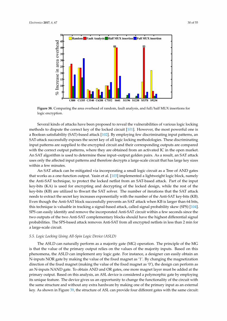
Electronics 2017, 6, 67 30 of 55
Electronics 2017, 6, 67 29 of 54
Meanwhile, the power and area overheads for each benchmark circuit depends on the number of
output bits. Figures 37 and 38 show the power‐delay and area overheads. On average, half MUX
insertions save more than 3.6× area overhead and 3.4× power‐delay overhead compared to those of
fault impact analysis, while full MUX insertions require less than half of the area overhead and half
of the power‐delay overhead that the fault impact analysis needs.
Figure 37. Comparing the power‐delay overhead of random, fault analysis, and full/half MUX
insertions for logic encryption.
Figure 38. Comparing the area overhead of random, fault analysis, and full/half MUX insertions for
logic encryption.
Several kinds of attacks have been proposed to reveal the vulnerabilities of various logic locking
methods to dispute the correct key of the locked circuit [101]. However, the most powerful one is a
Boolean satisfiability (SAT)‐based attack [102]. By employing few discriminating input patterns, an
SAT‐attack successfully exposes the secret key of all logic locking methodologies. These
discriminating input patterns are supplied to the encrypted circuit and their corresponding outputs
are compared with the correct output patterns, where they are obtained from an activated IC in the
open market. An SAT algorithm is used to determine these input–output golden pairs. As a result,
an SAT attack uses only the affected input patterns and therefore decrypts a large‐scale circuit that
has large key sizes within a few minutes.
An SAT attack can be mitigated via incorporating a small logic circuit as a Tree of AND gates
that works as a one‐function output. Yasin et al. [103] implemented a lightweight logic block, namely
the Anti‐SAT technique, to protect the locked netlist from an SAT‐based attack. Part of the input key‐
bits (KA) is used for encrypting and decrypting of the locked design, while the rest of the key‐bits
Figure 38. Comparing the area overhead of random, fault analysis, and full/half MUX insertions forlogic encryption.
Several kinds of attacks have been proposed to reveal the vulnerabilities of various logic lockingmethods to dispute the correct key of the locked circuit [101]. However, the most powerful one isa Boolean satisfiability (SAT)-based attack [102]. By employing few discriminating input patterns, anSAT-attack successfully exposes the secret key of all logic locking methodologies. These discriminatinginput patterns are supplied to the encrypted circuit and their corresponding outputs are comparedwith the correct output patterns, where they are obtained from an activated IC in the open market.An SAT algorithm is used to determine these input–output golden pairs. As a result, an SAT attackuses only the affected input patterns and therefore decrypts a large-scale circuit that has large key sizeswithin a few minutes.
An SAT attack can be mitigated via incorporating a small logic circuit as a Tree of AND gatesthat works as a one-function output. Yasin et al. [103] implemented a lightweight logic block, namelythe Anti-SAT technique, to protect the locked netlist from an SAT-based attack. Part of the inputkey-bits (KA) is used for encrypting and decrypting of the locked design, while the rest of thekey-bits (KB) are utilized to thwart the SAT solver. The number of iterations that the SAT attackneeds to extract the secret key increases exponentially with the number of the Anti-SAT key-bits (KB).Even though the Anti-SAT block successfully prevents an SAT attack when KB is larger than 64 bits,this technique is valuable in tracking a signal-based attack, called signal probability skew (SPS) [104].SPS can easily identify and remove the incorporated Anti-SAT circuit within a few seconds since thetwo outputs of the two Anti-SAT complementary blocks should have the highest differential signalprobabilities. The SPS-based attack removes Anti-SAT from all encrypted netlists in less than 2 min fora large-scale circuit.
5.5. Logic Locking Using All-Spin Logic Device (ASLD)
The ASLD can naturally perform as a majority gate (MG) operation. The principle of the MGis that the value of the primary output relies on the values of the majority inputs. Based on thisphenomena, the ASLD can implement any logic gate. For instance, a designer can easily obtain anN-inputs NOR gate by making the value of the fixed magnet as ‘1’. By changing the magnetizationdirection of the fixed magnet (making the value of the fixed magnet as ‘0’), the design can perform asan N-inputs NAND gate. To obtain AND and OR gates, one more magnet layer must be added at theprimary output. Based on this analysis, an ASL device is considered a polymorphic gate by employingits unique feature. The device gives us an opportunity to change the functionality of the circuit withthe same structure and without any extra hardware by making one of the primary input as an externalkey. As shown in Figure 39, the structure of ASL can provide four different gates with the same circuit:
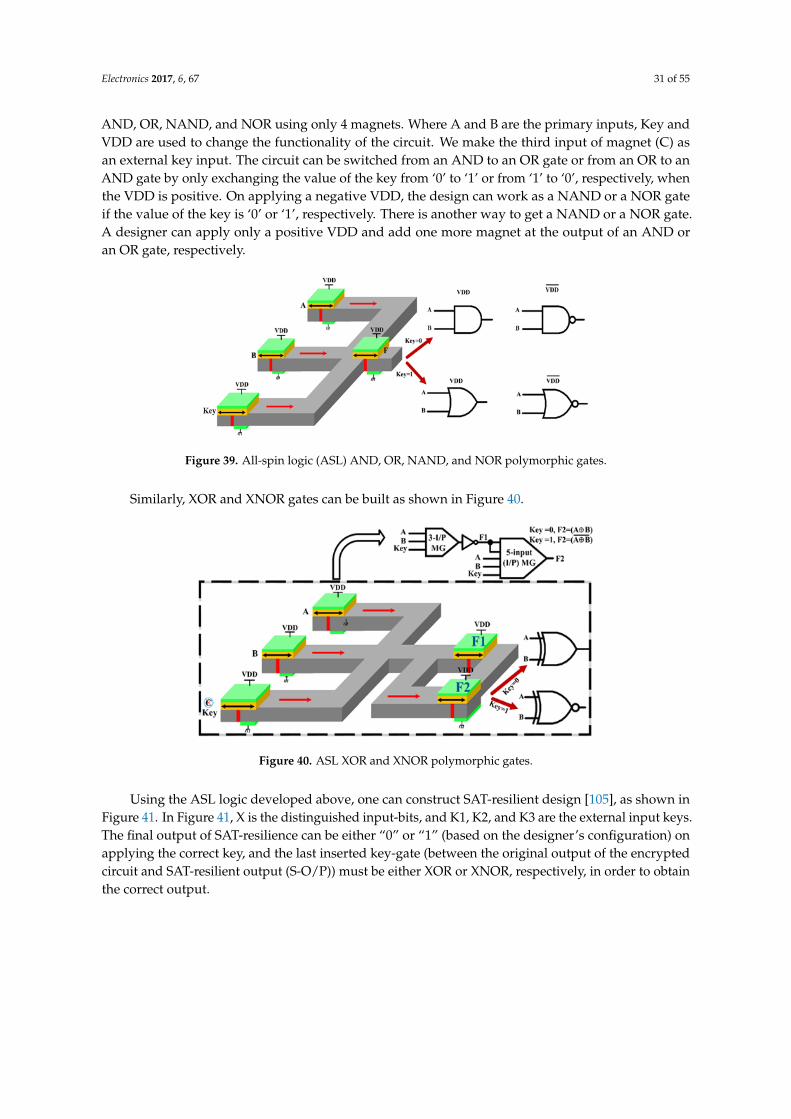
Electronics 2017, 6, 67 31 of 55
AND, OR, NAND, and NOR using only 4 magnets. Where A and B are the primary inputs, Key andVDD are used to change the functionality of the circuit. We make the third input of magnet (C) asan external key input. The circuit can be switched from an AND to an OR gate or from an OR to anAND gate by only exchanging the value of the key from ‘0’ to ‘1’ or from ‘1’ to ‘0’, respectively, whenthe VDD is positive. On applying a negative VDD, the design can work as a NAND or a NOR gateif the value of the key is ‘0’ or ‘1’, respectively. There is another way to get a NAND or a NOR gate.A designer can apply only a positive VDD and add one more magnet at the output of an AND oran OR gate, respectively.
Electronics 2017, 6, 67 30 of 54
(KB) are utilized to thwart the SAT solver. The number of iterations that the SAT attack needs to
extract the secret key increases exponentially with the number of the Anti‐SAT key‐bits (KB). Even
though the Anti‐SAT block successfully prevents an SAT attack when KB is larger than 64 bits, this
technique is valuable in tracking a signal‐based attack, called signal probability skew (SPS) [104]. SPS
can easily identify and remove the incorporated Anti‐SAT circuit within a few seconds since the two
outputs of the two Anti‐SAT complementary blocks should have the highest differential signal
probabilities. The SPS‐based attack removes Anti‐SAT from all encrypted netlists in less than 2 min
for a large‐scale circuit.
5.5. Logic Locking Using All‐Spin Logic Device (ASLD)
The ASLD can naturally perform as a majority gate (MG) operation. The principle of the MG is
that the value of the primary output relies on the values of the majority inputs. Based on this
phenomena, the ASLD can implement any logic gate. For instance, a designer can easily obtain an N‐
inputs NOR gate by making the value of the fixed magnet as ’1’. By changing the magnetization
direction of the fixed magnet (making the value of the fixed magnet as ’0’), the design can perform as
an N‐inputs NAND gate. To obtain AND and OR gates, one more magnet layer must be added at the
primary output. Based on this analysis, an ASL device is considered a polymorphic gate by
employing its unique feature. The device gives us an opportunity to change the functionality of the
circuit with the same structure and without any extra hardware by making one of the primary input
as an external key. As shown in Figure 39, the structure of ASL can provide four different gates with
the same circuit: AND, OR, NAND, and NOR using only 4 magnets. Where A and B are the primary
inputs, Key and VDD are used to change the functionality of the circuit. We make the third input of
magnet (C) as an external key input. The circuit can be switched from an AND to an OR gate or from
an OR to an AND gate by only exchanging the value of the key from ’0’ to ’1’ or from ’1’ to ’0’,
respectively, when the VDD is positive. On applying a negative VDD, the design can work as a
NAND or a NOR gate if the value of the key is ’0’ or ’1’, respectively. There is another way to get a
NAND or a NOR gate. A designer can apply only a positive VDD and add one more magnet at the
output of an AND or an OR gate, respectively.
Figure 39. All‐spin logic (ASL) AND, OR, NAND, and NOR polymorphic gates.
Similarly, XOR and XNOR gates can be built as shown in Figure 40.
Figure 39. All-spin logic (ASL) AND, OR, NAND, and NOR polymorphic gates.
Similarly, XOR and XNOR gates can be built as shown in Figure 40.Electronics 2017, 6, 67 31 of 54
Figure 40. ASL XOR and XNOR polymorphic gates.
Using the ASL logic developed above, one can construct SAT‐resilient design [105], as shown in
Figure 41. In Figure 41, X is the distinguished input‐bits, and K1, K2, and K3 are the external input
keys. The final output of SAT‐resilience can be either “0” or “1” (based on the designer’s configuration)
on applying the correct key, and the last inserted key‐gate (between the original output of the
encrypted circuit and SAT‐resilient output (S‐O/P)) must be either XOR or XNOR, respectively, in
order to obtain the correct output.
Figure 41. Scheme of satisfiability (SAT)‐resilient design using ASL.
5.6. Split Manufacturing
Split manufacturing is a way to partition digital circuits into many parts for security purposes.
The authors of [106] introduced a technique though supplying three‐dimensional combination
technology in split manufacturing. The authors implemented an algorithm to analyze the graph of a
circuit and disconnect certain wires from the design to prevent an attacker from obtaining the correct
design. Another proposal [107] was presented by Rajendran et al. whereby split manufacturing at
layer‐3 mental was examined. The benchmark circuits have been partitioned into many parts without
any connections among them. Afterwards, they developed a fault analysis algorithm in order to
switch the pins at layer 1 and 2 metals because the connections of the gates for any circuit are placed
in the first and second layers, which might help an attacker in an untrusted foundry for getting the
original design. The implementation of split manufacturing design before the second metal layer was
proposed by Vaidyanathan et al. [108]. Therefore, only the information at the gate level of the circuit
will be revealed to the untrusted companies. A similar method was achieved in detail for analog and
digital IC circuits in [109]. The technique against recognition IC‐based attacks has also been included,
supported by experimental results, where an SRAM with a 1 KB size and a digital‐to‐analog converter
with 14 bits have been used. Jagasivamani et al. [110] implemented many front end locking
Figure 40. ASL XOR and XNOR polymorphic gates.
Using the ASL logic developed above, one can construct SAT-resilient design [105], as shown inFigure 41. In Figure 41, X is the distinguished input-bits, and K1, K2, and K3 are the external input keys.The final output of SAT-resilience can be either “0” or “1” (based on the designer’s configuration) onapplying the correct key, and the last inserted key-gate (between the original output of the encryptedcircuit and SAT-resilient output (S-O/P)) must be either XOR or XNOR, respectively, in order to obtainthe correct output.
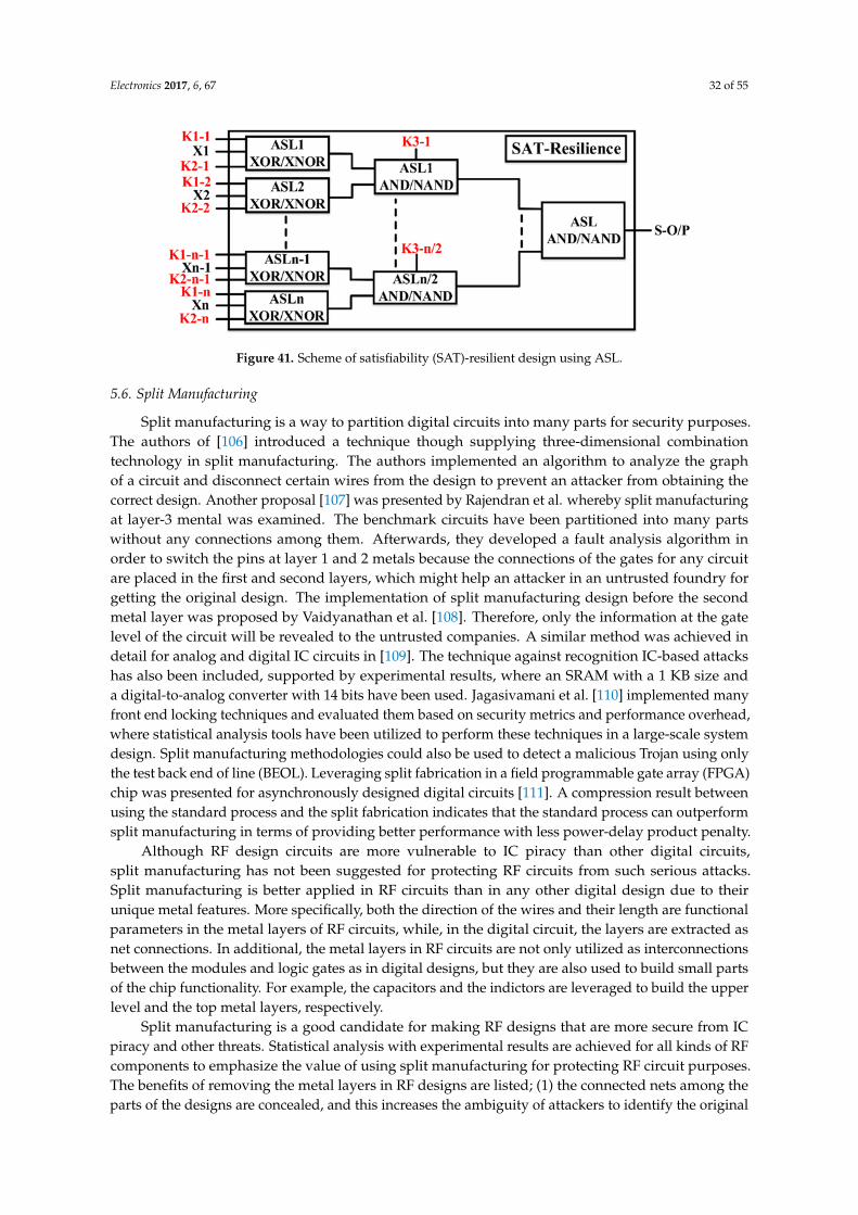
Electronics 2017, 6, 67 32 of 55
Electronics 2017, 6, 67 31 of 54
Figure 40. ASL XOR and XNOR polymorphic gates.
Using the ASL logic developed above, one can construct SAT‐resilient design [105], as shown in
Figure 41. In Figure 41, X is the distinguished input‐bits, and K1, K2, and K3 are the external input
keys. The final output of SAT‐resilience can be either “0” or “1” (based on the designer’s configuration)
on applying the correct key, and the last inserted key‐gate (between the original output of the
encrypted circuit and SAT‐resilient output (S‐O/P)) must be either XOR or XNOR, respectively, in
order to obtain the correct output.
Figure 41. Scheme of satisfiability (SAT)‐resilient design using ASL.
5.6. Split Manufacturing
Split manufacturing is a way to partition digital circuits into many parts for security purposes.
The authors of [106] introduced a technique though supplying three‐dimensional combination
technology in split manufacturing. The authors implemented an algorithm to analyze the graph of a
circuit and disconnect certain wires from the design to prevent an attacker from obtaining the correct
design. Another proposal [107] was presented by Rajendran et al. whereby split manufacturing at
layer‐3 mental was examined. The benchmark circuits have been partitioned into many parts without
any connections among them. Afterwards, they developed a fault analysis algorithm in order to
switch the pins at layer 1 and 2 metals because the connections of the gates for any circuit are placed
in the first and second layers, which might help an attacker in an untrusted foundry for getting the
original design. The implementation of split manufacturing design before the second metal layer was
proposed by Vaidyanathan et al. [108]. Therefore, only the information at the gate level of the circuit
will be revealed to the untrusted companies. A similar method was achieved in detail for analog and
digital IC circuits in [109]. The technique against recognition IC‐based attacks has also been included,
supported by experimental results, where an SRAM with a 1 KB size and a digital‐to‐analog converter
with 14 bits have been used. Jagasivamani et al. [110] implemented many front end locking
Figure 41. Scheme of satisfiability (SAT)-resilient design using ASL.
5.6. Split Manufacturing
Split manufacturing is a way to partition digital circuits into many parts for security purposes.The authors of [106] introduced a technique though supplying three-dimensional combinationtechnology in split manufacturing. The authors implemented an algorithm to analyze the graphof a circuit and disconnect certain wires from the design to prevent an attacker from obtaining thecorrect design. Another proposal [107] was presented by Rajendran et al. whereby split manufacturingat layer-3 mental was examined. The benchmark circuits have been partitioned into many partswithout any connections among them. Afterwards, they developed a fault analysis algorithm inorder to switch the pins at layer 1 and 2 metals because the connections of the gates for any circuitare placed in the first and second layers, which might help an attacker in an untrusted foundry forgetting the original design. The implementation of split manufacturing design before the secondmetal layer was proposed by Vaidyanathan et al. [108]. Therefore, only the information at the gatelevel of the circuit will be revealed to the untrusted companies. A similar method was achieved indetail for analog and digital IC circuits in [109]. The technique against recognition IC-based attackshas also been included, supported by experimental results, where an SRAM with a 1 KB size anda digital-to-analog converter with 14 bits have been used. Jagasivamani et al. [110] implemented manyfront end locking techniques and evaluated them based on security metrics and performance overhead,where statistical analysis tools have been utilized to perform these techniques in a large-scale systemdesign. Split manufacturing methodologies could also be used to detect a malicious Trojan using onlythe test back end of line (BEOL). Leveraging split fabrication in a field programmable gate array (FPGA)chip was presented for asynchronously designed digital circuits [111]. A compression result betweenusing the standard process and the split fabrication indicates that the standard process can outperformsplit manufacturing in terms of providing better performance with less power-delay product penalty.
Although RF design circuits are more vulnerable to IC piracy than other digital circuits,split manufacturing has not been suggested for protecting RF circuits from such serious attacks.Split manufacturing is better applied in RF circuits than in any other digital design due to theirunique metal features. More specifically, both the direction of the wires and their length are functionalparameters in the metal layers of RF circuits, while, in the digital circuit, the layers are extracted asnet connections. In additional, the metal layers in RF circuits are not only utilized as interconnectionsbetween the modules and logic gates as in digital designs, but they are also used to build small partsof the chip functionality. For example, the capacitors and the indictors are leveraged to build the upperlevel and the top metal layers, respectively.
Split manufacturing is a good candidate for making RF designs that are more secure from ICpiracy and other threats. Statistical analysis with experimental results are achieved for all kinds of RFcomponents to emphasize the value of using split manufacturing for protecting RF circuit purposes.The benefits of removing the metal layers in RF designs are listed; (1) the connected nets among theparts of the designs are concealed, and this increases the ambiguity of attackers to identify the original
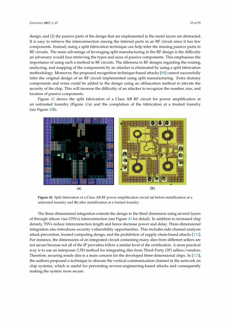
Electronics 2017, 6, 67 33 of 55
design, and (2) the passive parts of the design that are implemented in the metal layers are abstracted.It is easy to retrieve the interconnection among the internal parts in an RF circuit since it has fewcomponents. Instead, using a split fabrication technique can help infer the missing passive parts inRF circuits. The main advantage of leveraging split manufacturing in the RF design is the difficultyan adversary would face retrieving the types and sizes of passive components. This emphasizes theimportance of using such a method in RF circuits. The dilemma in RF designs regarding the routing,analyzing, and mapping of the components by an attacker is eliminated by using a split fabricationmethodology. Moreover, the proposed recognition technique-based attacks [88] cannot successfullyinfer the original design of an RF circuit implemented using split manufacturing. Extra dummycomponents and wires could be added to the design using an obfuscation method to elevate thesecurity of the chip. This will increase the difficulty of an attacker to recognize the number, size, andlocation of passive components.
Figure 42 shows the split fabrication of a Class AB RF circuit for power amplification atan untrusted foundry (Figure 42a) and the completion of the fabrication at a trusted foundry(see Figure 42b).
Electronics 2017, 6, 67 32 of 54
techniques and evaluated them based on security metrics and performance overhead, where
statistical analysis tools have been utilized to perform these techniques in a large‐scale system design.
Split manufacturing methodologies could also be used to detect a malicious Trojan using only the
test back end of line (BEOL). Leveraging split fabrication in a field programmable gate array (FPGA)
chip was presented for asynchronously designed digital circuits [111]. A compression result between
using the standard process and the split fabrication indicates that the standard process can
outperform split manufacturing in terms of providing better performance with less power‐delay
product penalty.
Although RF design circuits are more vulnerable to IC piracy than other digital circuits, split
manufacturing has not been suggested for protecting RF circuits from such serious attacks. Split
manufacturing is better applied in RF circuits than in any other digital design due to their unique
metal features. More specifically, both the direction of the wires and their length are functional
parameters in the metal layers of RF circuits, while, in the digital circuit, the layers are extracted as
net connections. In additional, the metal layers in RF circuits are not only utilized as interconnections
between the modules and logic gates as in digital designs, but they are also used to build small parts
of the chip functionality. For example, the capacitors and the indictors are leveraged to build the
upper level and the top metal layers, respectively.
Split manufacturing is a good candidate for making RF designs that are more secure from IC
piracy and other threats. Statistical analysis with experimental results are achieved for all kinds of RF
components to emphasize the value of using split manufacturing for protecting RF circuit purposes.
The benefits of removing the metal layers in RF designs are listed; (1) the connected nets among the
parts of the designs are concealed, and this increases the ambiguity of attackers to identify the original
design, and (2) the passive parts of the design that are implemented in the metal layers are abstracted.
It is easy to retrieve the interconnection among the internal parts in an RF circuit since it has few
components. Instead, using a split fabrication technique can help infer the missing passive parts in
RF circuits. The main advantage of leveraging split manufacturing in the RF design is the difficulty
an adversary would face retrieving the types and sizes of passive components. This emphasizes the
importance of using such a method in RF circuits. The dilemma in RF designs regarding the routing,
analyzing, and mapping of the components by an attacker is eliminated by using a split fabrication
methodology. Moreover, the proposed recognition technique‐based attacks [88] cannot successfully
infer the original design of an RF circuit implemented using split manufacturing. Extra dummy
components and wires could be added to the design using an obfuscation method to elevate the
security of the chip. This will increase the difficulty of an attacker to recognize the number, size, and
location of passive components.
Figure 42 shows the split fabrication of a Class AB RF circuit for power amplification at an
untrusted foundry (Figure 42a) and the completion of the fabrication at a trusted foundry (see Figure
42b).
(a) (b)
Figure 42. Split fabrication of a Class AB RF power amplification circuit (a) before metallization at auntrusted foundry and (b) after metallization at a trusted foundry.
The three-dimensional integration extends the design to the third dimension using several layersof through silicon vias (TSVs) interconnection (see Figure 43 for detail). In addition to increased chipdensity, TSVs reduce interconnection length and hence decrease power and delay. Three-dimensionalintegration also introduces security vulnerability opportunities. This includes side channel analysisattack prevention, trusted computing design, and the prohibition of supply-chain-based attacks [112].For instance, the dimensions of an integrated circuit containing many dies from different sellers arenot secure because not all of the IP providers follow a similar level of die certification. A more practicalway is to use an interposer 2.5D method for integrating dies from Third-Party (3P) sellers/vendors.Therefore, securing inside dies is a main concern for the developed three-dimensional chips. In [113],the authors proposed a technique to obscure the vertical communication channel in the network onchip systems, which is useful for preventing reverse-engineering-based attacks and consequentlymaking the system more secure.
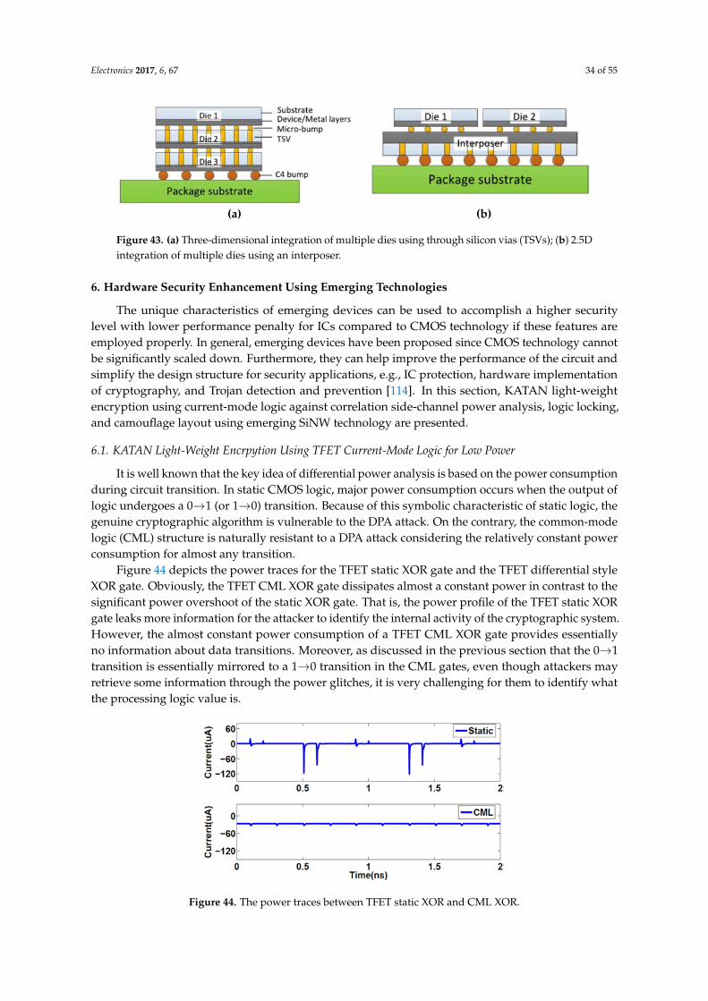
Electronics 2017, 6, 67 34 of 55
Electronics 2017, 6, 67 33 of 54
Figure 42. Split fabrication of a Class AB RF power amplification circuit (a) before metallization at a
untrusted foundry and (b) after metallization at a trusted foundry.
The three‐dimensional integration extends the design to the third dimension using several layers
of through silicon vias (TSVs) interconnection (see Figure 43 for detail). In addition to increased chip
density, TSVs reduce interconnection length and hence decrease power and delay. Three‐
dimensional integration also introduces security vulnerability opportunities. This includes side
channel analysis attack prevention, trusted computing design, and the prohibition of supply‐chain‐
based attacks [112]. For instance, the dimensions of an integrated circuit containing many dies from
different sellers are not secure because not all of the IP providers follow a similar level of die
certification. A more practical way is to use an interposer 2.5D method for integrating dies from
Third‐Party (3P) sellers/vendors. Therefore, securing inside dies is a main concern for the developed
three‐dimensional chips. In [113], the authors proposed a technique to obscure the vertical
communication channel in the network on chip systems, which is useful for preventing reverse‐
engineering‐based attacks and consequently making the system more secure.
(a) (b)
Figure 43. (a) Three‐dimensional integration of multiple dies using through silicon vias (TSVs); (b)
2.5D integration of multiple dies using an interposer.
6. Hardware Security Enhancement Using Emerging Technologies
The unique characteristics of emerging devices can be used to accomplish a higher security level
with lower performance penalty for ICs compared to CMOS technology if these features are
employed properly. In general, emerging devices have been proposed since CMOS technology
cannot be significantly scaled down. Furthermore, they can help improve the performance of the
circuit and simplify the design structure for security applications, e.g., IC protection, hardware
implementation of cryptography, and Trojan detection and prevention [114]. In this section, KATAN
light‐weight encryption using current‐mode logic against correlation side‐channel power analysis,
logic locking, and camouflage layout using emerging SiNW technology are presented.
6.1. KATAN Light‐Weight Encrpytion Using TFET Current‐Mode Logic for Low Power
It is well known that the key idea of differential power analysis is based on the power
consumption during circuit transition. In static CMOS logic, major power consumption occurs when
the output of logic undergoes a 0→1 (or 1→0) transition. Because of this symbolic characteristic of
static logic, the genuine cryptographic algorithm is vulnerable to the DPA attack. On the contrary,
the common‐mode logic (CML) structure is naturally resistant to a DPA attack considering the
relatively constant power consumption for almost any transition.
Figure 44 depicts the power traces for the TFET static XOR gate and the TFET differential style
XOR gate. Obviously, the TFET CML XOR gate dissipates almost a constant power in contrast to the
significant power overshoot of the static XOR gate. That is, the power profile of the TFET static XOR
gate leaks more information for the attacker to identify the internal activity of the cryptographic
system. However, the almost constant power consumption of a TFET CML XOR gate provides
essentially no information about data transitions. Moreover, as discussed in the previous section that
the 0→1 transition is essentially mirrored to a 1→0 transition in the CML gates, even though attackers
Figure 43. (a) Three-dimensional integration of multiple dies using through silicon vias (TSVs); (b) 2.5Dintegration of multiple dies using an interposer.
6. Hardware Security Enhancement Using Emerging Technologies
The unique characteristics of emerging devices can be used to accomplish a higher securitylevel with lower performance penalty for ICs compared to CMOS technology if these features areemployed properly. In general, emerging devices have been proposed since CMOS technology cannotbe significantly scaled down. Furthermore, they can help improve the performance of the circuit andsimplify the design structure for security applications, e.g., IC protection, hardware implementationof cryptography, and Trojan detection and prevention [114]. In this section, KATAN light-weightencryption using current-mode logic against correlation side-channel power analysis, logic locking,and camouflage layout using emerging SiNW technology are presented.
6.1. KATAN Light-Weight Encrpytion Using TFET Current-Mode Logic for Low Power
It is well known that the key idea of differential power analysis is based on the power consumptionduring circuit transition. In static CMOS logic, major power consumption occurs when the output oflogic undergoes a 0→1 (or 1→0) transition. Because of this symbolic characteristic of static logic, thegenuine cryptographic algorithm is vulnerable to the DPA attack. On the contrary, the common-modelogic (CML) structure is naturally resistant to a DPA attack considering the relatively constant powerconsumption for almost any transition.
Figure 44 depicts the power traces for the TFET static XOR gate and the TFET differential styleXOR gate. Obviously, the TFET CML XOR gate dissipates almost a constant power in contrast to thesignificant power overshoot of the static XOR gate. That is, the power profile of the TFET static XORgate leaks more information for the attacker to identify the internal activity of the cryptographic system.However, the almost constant power consumption of a TFET CML XOR gate provides essentiallyno information about data transitions. Moreover, as discussed in the previous section that the 0→1transition is essentially mirrored to a 1→0 transition in the CML gates, even though attackers mayretrieve some information through the power glitches, it is very challenging for them to identify whatthe processing logic value is.
Electronics 2017, 6, 67 34 of 54
may retrieve some information through the power glitches, it is very challenging for them to identify
what the processing logic value is.
Figure 44. The power traces between TFET static XOR and CML XOR.
Due to the large area and high power consumption, using CML to implement cryptographic
hardware is not common—especially in lightweight cryptographic systems. To protect cryptographic
circuits against DPA attacks, researchers often employ other techniques [115]. These solutions incur
a significant computation cost where the cryptography already involves massive computation and
consumes a relatively large power and area. As such, lower‐power, TFET‐based CML could be
especially valuable when considering devices for the IoT, wireless sensor nodes, etc. Lacking an
effective defense mechanism, hardware in these spaces can be substantially more
vulnerable/susceptible to hardware attacks such as DPA. To address these challenges, we consider
the impact of TFET‐based CML on a 32‐bit KATAN cipher. Here, a correlation power analysis (CPA)
on KATAN32 is described to disclose the two key values. Initially, four selected plaintexts are loaded
into the two registers and the 80 bit keys are all set to zero. Note that, in real cases, the key is the
attackers’ target and is unknown to attackers. When the start signal is received, KATAN32 begins
encryption. Figure 45 shows the proposed CPA attack flow on KATAN32. Each selected plaintext
and the hypothetical Subkeys Ka and Kb are calculated to achieve the intermediate values “v” matrix.
Then, intermediate results are further calculated by the power model, which is defined as the
Hamming weight model. The results from the Hamming weight model are defined as the
hypothetical power consumption.
Figure 45. Correctional power analysis flow on the KATAN cipher.
The predicted power consumption is then compared with the measured real power
consumption by the correlation coefficient formula as given in Equation (9). The highest correlation
coefficient result stands for the correctly guessed keys. In this case, the keys ‘00’ reflect the largest
correlation coefficient value. The next round follows the same mechanism, but with slightly different
Figure 44. The power traces between TFET static XOR and CML XOR.
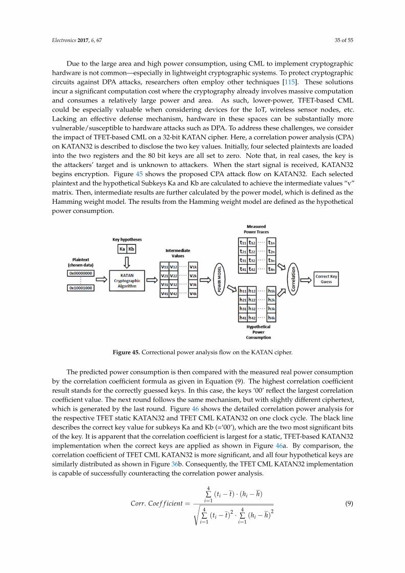
Electronics 2017, 6, 67 35 of 55
Due to the large area and high power consumption, using CML to implement cryptographichardware is not common—especially in lightweight cryptographic systems. To protect cryptographiccircuits against DPA attacks, researchers often employ other techniques [115]. These solutionsincur a significant computation cost where the cryptography already involves massive computationand consumes a relatively large power and area. As such, lower-power, TFET-based CMLcould be especially valuable when considering devices for the IoT, wireless sensor nodes, etc.Lacking an effective defense mechanism, hardware in these spaces can be substantially morevulnerable/susceptible to hardware attacks such as DPA. To address these challenges, we considerthe impact of TFET-based CML on a 32-bit KATAN cipher. Here, a correlation power analysis (CPA)on KATAN32 is described to disclose the two key values. Initially, four selected plaintexts are loadedinto the two registers and the 80 bit keys are all set to zero. Note that, in real cases, the key isthe attackers’ target and is unknown to attackers. When the start signal is received, KATAN32begins encryption. Figure 45 shows the proposed CPA attack flow on KATAN32. Each selectedplaintext and the hypothetical Subkeys Ka and Kb are calculated to achieve the intermediate values “v”matrix. Then, intermediate results are further calculated by the power model, which is defined as theHamming weight model. The results from the Hamming weight model are defined as the hypotheticalpower consumption.
Electronics 2017, 6, 67 34 of 54
may retrieve some information through the power glitches, it is very challenging for them to identify
what the processing logic value is.
Figure 44. The power traces between TFET static XOR and CML XOR.
Due to the large area and high power consumption, using CML to implement cryptographic
hardware is not common—especially in lightweight cryptographic systems. To protect cryptographic
circuits against DPA attacks, researchers often employ other techniques [115]. These solutions incur
a significant computation cost where the cryptography already involves massive computation and
consumes a relatively large power and area. As such, lower‐power, TFET‐based CML could be
especially valuable when considering devices for the IoT, wireless sensor nodes, etc. Lacking an
effective defense mechanism, hardware in these spaces can be substantially more
vulnerable/susceptible to hardware attacks such as DPA. To address these challenges, we consider
the impact of TFET‐based CML on a 32‐bit KATAN cipher. Here, a correlation power analysis (CPA)
on KATAN32 is described to disclose the two key values. Initially, four selected plaintexts are loaded
into the two registers and the 80 bit keys are all set to zero. Note that, in real cases, the key is the
attackers’ target and is unknown to attackers. When the start signal is received, KATAN32 begins
encryption. Figure 45 shows the proposed CPA attack flow on KATAN32. Each selected plaintext
and the hypothetical Subkeys Ka and Kb are calculated to achieve the intermediate values “v” matrix.
Then, intermediate results are further calculated by the power model, which is defined as the
Hamming weight model. The results from the Hamming weight model are defined as the
hypothetical power consumption.
Figure 45. Correctional power analysis flow on the KATAN cipher.
The predicted power consumption is then compared with the measured real power
consumption by the correlation coefficient formula as given in Equation (9). The highest correlation
coefficient result stands for the correctly guessed keys. In this case, the keys ‘00’ reflect the largest
correlation coefficient value. The next round follows the same mechanism, but with slightly different
Figure 45. Correctional power analysis flow on the KATAN cipher.
The predicted power consumption is then compared with the measured real power consumptionby the correlation coefficient formula as given in Equation (9). The highest correlation coefficientresult stands for the correctly guessed keys. In this case, the keys ‘00’ reflect the largest correlationcoefficient value. The next round follows the same mechanism, but with slightly different ciphertext,which is generated by the last round. Figure 46 shows the detailed correlation power analysis forthe respective TFET static KATAN32 and TFET CML KATAN32 on one clock cycle. The black linedescribes the correct key value for subkeys Ka and Kb (=‘00’), which are the two most significant bitsof the key. It is apparent that the correlation coefficient is largest for a static, TFET-based KATAN32implementation when the correct keys are applied as shown in Figure 46a. By comparison, thecorrelation coefficient of TFET CML KATAN32 is more significant, and all four hypothetical keys aresimilarly distributed as shown in Figure 36b. Consequently, the TFET CML KATAN32 implementationis capable of successfully counteracting the correlation power analysis.
Corr. Coe f f icient =
4∑
i=1(ti − t) · (hi − h)√
4∑
i=1(ti − t)2 ·
4∑
i=1(hi − h)
2(9)
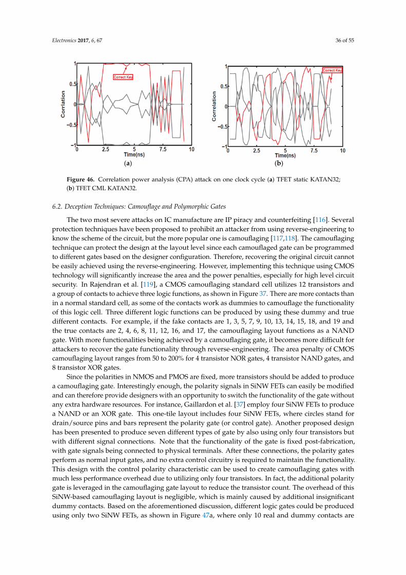
Electronics 2017, 6, 67 36 of 55
Electronics 2017, 6, 67 35 of 54
ciphertext, which is generated by the last round. Figure 46 shows the detailed correlation power
analysis for the respective TFET static KATAN32 and TFET CML KATAN32 on one clock cycle. The
black line describes the correct key value for subkeys Ka and Kb (=‘00’), which are the two most
significant bits of the key. It is apparent that the correlation coefficient is largest for a static, TFET‐
based KATAN32 implementation when the correct keys are applied as shown in Figure 46a. By
comparison, the correlation coefficient of TFET CML KATAN32 is more significant, and all four
hypothetical keys are similarly distributed as shown in Figure 36b. Consequently, the TFET CML
KATAN32 implementation is capable of successfully counteracting the correlation power analysis.
4
1
4
1
22
4
1
)()(
)()(.
i iii
iii
hhtt
hhtttCoefficienCorr (9)
(a) (b)
Figure 46. Correlation power analysis (CPA) attack on one clock cycle (a) TFET static KATAN32; (b)
TFET CML KATAN32.
6.2. Deception Techniques: Camouflage and Polymorphic Gates
The two most severe attacks on IC manufacture are IP piracy and counterfeiting [116]. Several
protection techniques have been proposed to prohibit an attacker from using reverse‐engineering to
know the scheme of the circuit, but the more popular one is camouflaging [117,118]. The
camouflaging technique can protect the design at the layout level since each camouflaged gate can
be programmed to different gates based on the designer configuration. Therefore, recovering the
original circuit cannot be easily achieved using the reverse‐engineering. However, implementing this
technique using CMOS technology will significantly increase the area and the power penalties,
especially for high level circuit security. In Rajendran et al. [119], a CMOS camouflaging standard cell
utilizes 12 transistors and a group of contacts to achieve three logic functions, as shown in Figure 37.
There are more contacts than in a normal standard cell, as some of the contacts work as dummies to
camouflage the functionality of this logic cell. Three different logic functions can be produced by
using these dummy and true different contacts. For example, if the fake contacts are 1, 3, 5, 7, 9, 10,
13, 14, 15, 18, and 19 and the true contacts are 2, 4, 6, 8, 11, 12, 16, and 17, the camouflaging layout
functions as a NAND gate. With more functionalities being achieved by a camouflaging gate, it
becomes more difficult for attackers to recover the gate functionality through reverse‐engineering.
The area penalty of CMOS camouflaging layout ranges from 50 to 200% for 4 transistor NOR gates,
4 transistor NAND gates, and 8 transistor XOR gates.
Since the polarities in NMOS and PMOS are fixed, more transistors should be added to produce
a camouflaging gate. Interestingly enough, the polarity signals in SiNW FETs can easily be modified
and can therefore provide designers with an opportunity to switch the functionality of the gate
without any extra hardware resources. For instance, Gaillardon et al. [37] employ four SiNW FETs to
produce a NAND or an XOR gate. This one‐tile layout includes four SiNW FETs, where circles stand
Figure 46. Correlation power analysis (CPA) attack on one clock cycle (a) TFET static KATAN32;(b) TFET CML KATAN32.
6.2. Deception Techniques: Camouflage and Polymorphic Gates
The two most severe attacks on IC manufacture are IP piracy and counterfeiting [116]. Severalprotection techniques have been proposed to prohibit an attacker from using reverse-engineering toknow the scheme of the circuit, but the more popular one is camouflaging [117,118]. The camouflagingtechnique can protect the design at the layout level since each camouflaged gate can be programmedto different gates based on the designer configuration. Therefore, recovering the original circuit cannotbe easily achieved using the reverse-engineering. However, implementing this technique using CMOStechnology will significantly increase the area and the power penalties, especially for high level circuitsecurity. In Rajendran et al. [119], a CMOS camouflaging standard cell utilizes 12 transistors anda group of contacts to achieve three logic functions, as shown in Figure 37. There are more contacts thanin a normal standard cell, as some of the contacts work as dummies to camouflage the functionalityof this logic cell. Three different logic functions can be produced by using these dummy and truedifferent contacts. For example, if the fake contacts are 1, 3, 5, 7, 9, 10, 13, 14, 15, 18, and 19 andthe true contacts are 2, 4, 6, 8, 11, 12, 16, and 17, the camouflaging layout functions as a NANDgate. With more functionalities being achieved by a camouflaging gate, it becomes more difficult forattackers to recover the gate functionality through reverse-engineering. The area penalty of CMOScamouflaging layout ranges from 50 to 200% for 4 transistor NOR gates, 4 transistor NAND gates, and8 transistor XOR gates.
Since the polarities in NMOS and PMOS are fixed, more transistors should be added to producea camouflaging gate. Interestingly enough, the polarity signals in SiNW FETs can easily be modifiedand can therefore provide designers with an opportunity to switch the functionality of the gate withoutany extra hardware resources. For instance, Gaillardon et al. [37] employ four SiNW FETs to producea NAND or an XOR gate. This one-tile layout includes four SiNW FETs, where circles stand fordrain/source pins and bars represent the polarity gate (or control gate). Another proposed designhas been presented to produce seven different types of gate by also using only four transistors butwith different signal connections. Note that the functionality of the gate is fixed post-fabrication,with gate signals being connected to physical terminals. After these connections, the polarity gatesperform as normal input gates, and no extra control circuitry is required to maintain the functionality.This design with the control polarity characteristic can be used to create camouflaging gates withmuch less performance overhead due to utilizing only four transistors. In fact, the additional polaritygate is leveraged in the camouflaging gate layout to reduce the transistor count. The overhead of thisSiNW-based camouflaging layout is negligible, which is mainly caused by additional insignificantdummy contacts. Based on the aforementioned discussion, different logic gates could be producedusing only two SiNW FETs, as shown in Figure 47a, where only 10 real and dummy contacts are
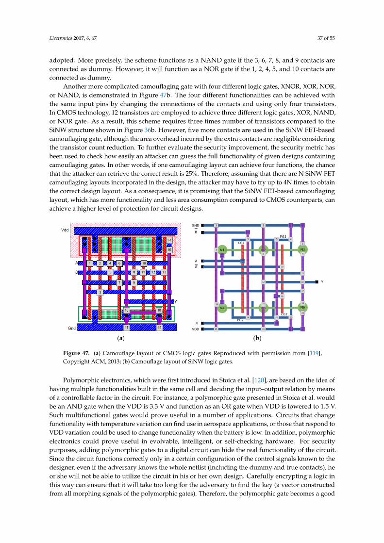
Electronics 2017, 6, 67 37 of 55
adopted. More precisely, the scheme functions as a NAND gate if the 3, 6, 7, 8, and 9 contacts areconnected as dummy. However, it will function as a NOR gate if the 1, 2, 4, 5, and 10 contacts areconnected as dummy.
Another more complicated camouflaging gate with four different logic gates, XNOR, XOR, NOR,or NAND, is demonstrated in Figure 47b. The four different functionalities can be achieved withthe same input pins by changing the connections of the contacts and using only four transistors.In CMOS technology, 12 transistors are employed to achieve three different logic gates, XOR, NAND,or NOR gate. As a result, this scheme requires three times number of transistors compared to theSiNW structure shown in Figure 36b. However, five more contacts are used in the SiNW FET-basedcamouflaging gate, although the area overhead incurred by the extra contacts are negligible consideringthe transistor count reduction. To further evaluate the security improvement, the security metric hasbeen used to check how easily an attacker can guess the full functionality of given designs containingcamouflaging gates. In other words, if one camouflaging layout can achieve four functions, the chancethat the attacker can retrieve the correct result is 25%. Therefore, assuming that there are N SiNW FETcamouflaging layouts incorporated in the design, the attacker may have to try up to 4N times to obtainthe correct design layout. As a consequence, it is promising that the SiNW FET-based camouflaginglayout, which has more functionality and less area consumption compared to CMOS counterparts, canachieve a higher level of protection for circuit designs.
Electronics 2017, 6, 67 36 of 54
for drain/source pins and bars represent the polarity gate (or control gate). Another proposed design
has been presented to produce seven different types of gate by also using only four transistors but
with different signal connections. Note that the functionality of the gate is fixed post‐fabrication, with
gate signals being connected to physical terminals. After these connections, the polarity gates perform
as normal input gates, and no extra control circuitry is required to maintain the functionality. This
design with the control polarity characteristic can be used to create camouflaging gates with much
less performance overhead due to utilizing only four transistors. In fact, the additional polarity gate
is leveraged in the camouflaging gate layout to reduce the transistor count. The overhead of this
SiNW‐based camouflaging layout is negligible, which is mainly caused by additional insignificant
dummy contacts. Based on the aforementioned discussion, different logic gates could be produced
using only two SiNW FETs, as shown in Figure 47a, where only 10 real and dummy contacts are
adopted. More precisely, the scheme functions as a NAND gate if the 3, 6, 7, 8, and 9 contacts are
connected as dummy. However, it will function as a NOR gate if the 1, 2, 4, 5, and 10 contacts are
connected as dummy.
Another more complicated camouflaging gate with four different logic gates, XNOR, XOR, NOR,
or NAND, is demonstrated in Figure 47b. The four different functionalities can be achieved with the
same input pins by changing the connections of the contacts and using only four transistors. In CMOS
technology, 12 transistors are employed to achieve three different logic gates, XOR, NAND, or NOR
gate. As a result, this scheme requires three times number of transistors compared to the SiNW
structure shown in Figure 36b. However, five more contacts are used in the SiNW FET‐based
camouflaging gate, although the area overhead incurred by the extra contacts are negligible
considering the transistor count reduction. To further evaluate the security improvement, the security
metric has been used to check how easily an attacker can guess the full functionality of given designs
containing camouflaging gates. In other words, if one camouflaging layout can achieve four functions,
the chance that the attacker can retrieve the correct result is 25%. Therefore, assuming that there are
N SiNW FET camouflaging layouts incorporated in the design, the attacker may have to try up to 4N
times to obtain the correct design layout. As a consequence, it is promising that the SiNW FET‐based
camouflaging layout, which has more functionality and less area consumption compared to CMOS
counterparts, can achieve a higher level of protection for circuit designs.
(a) (b)
Figure 47. (a) Camouflage layout of CMOS logic gates Reproduced with permission from [119],
Copyright ACM, 2013; (b) Camouflage layout of SiNW logic gates.
Polymorphic electronics, which were first introduced in Stoica et al. [120], are based on the idea
of having multiple functionalities built in the same cell and deciding the input–output relation by
means of a controllable factor in the circuit. For instance, a polymorphic gate presented in Stoica et
al. would be an AND gate when the VDD is 3.3 V and function as an OR gate when VDD is lowered
to 1.5 V. Such multifunctional gates would prove useful in a number of applications. Circuits that
Figure 47. (a) Camouflage layout of CMOS logic gates Reproduced with permission from [119],Copyright ACM, 2013; (b) Camouflage layout of SiNW logic gates.
Polymorphic electronics, which were first introduced in Stoica et al. [120], are based on the idea ofhaving multiple functionalities built in the same cell and deciding the input–output relation by meansof a controllable factor in the circuit. For instance, a polymorphic gate presented in Stoica et al. wouldbe an AND gate when the VDD is 3.3 V and function as an OR gate when VDD is lowered to 1.5 V.Such multifunctional gates would prove useful in a number of applications. Circuits that changefunctionality with temperature variation can find use in aerospace applications, or those that respond toVDD variation could be used to change functionality when the battery is low. In addition, polymorphicelectronics could prove useful in evolvable, intelligent, or self-checking hardware. For securitypurposes, adding polymorphic gates to a digital circuit can hide the real functionality of the circuit.Since the circuit functions correctly only in a certain configuration of the control signals known to thedesigner, even if the adversary knows the whole netlist (including the dummy and true contacts), heor she will not be able to utilize the circuit in his or her own design. Carefully encrypting a logic inthis way can ensure that it will take too long for the adversary to find the key (a vector constructedfrom all morphing signals of the polymorphic gates). Therefore, the polymorphic gate becomes a good
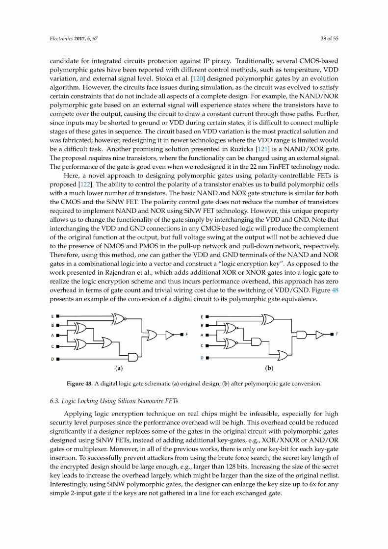
Electronics 2017, 6, 67 38 of 55
candidate for integrated circuits protection against IP piracy. Traditionally, several CMOS-basedpolymorphic gates have been reported with different control methods, such as temperature, VDDvariation, and external signal level. Stoica et al. [120] designed polymorphic gates by an evolutionalgorithm. However, the circuits face issues during simulation, as the circuit was evolved to satisfycertain constraints that do not include all aspects of a complete design. For example, the NAND/NORpolymorphic gate based on an external signal will experience states where the transistors have tocompete over the output, causing the circuit to draw a constant current through those paths. Further,since inputs may be shorted to ground or VDD during certain states, it is difficult to connect multiplestages of these gates in sequence. The circuit based on VDD variation is the most practical solution andwas fabricated; however, redesigning it in newer technologies where the VDD range is limited wouldbe a difficult task. Another promising solution presented in Ruzicka [121] is a NAND/XOR gate.The proposal requires nine transistors, where the functionality can be changed using an external signal.The performance of the gate is good even when we redesigned it in the 22 nm FinFET technology node.
Here, a novel approach to designing polymorphic gates using polarity-controllable FETs isproposed [122]. The ability to control the polarity of a transistor enables us to build polymorphic cellswith a much lower number of transistors. The basic NAND and NOR gate structure is similar for boththe CMOS and the SiNW FET. The polarity control gate does not reduce the number of transistorsrequired to implement NAND and NOR using SiNW FET technology. However, this unique propertyallows us to change the functionality of the gate simply by interchanging the VDD and GND. Note thatinterchanging the VDD and GND connections in any CMOS-based logic will produce the complementof the original function at the output, but full voltage swing at the output will not be achieved dueto the presence of NMOS and PMOS in the pull-up network and pull-down network, respectively.Therefore, using this method, one can gather the VDD and GND terminals of the NAND and NORgates in a combinational logic into a vector and construct a “logic encryption key”. As opposed to thework presented in Rajendran et al., which adds additional XOR or XNOR gates into a logic gate torealize the logic encryption scheme and thus incurs performance overhead, this approach has zerooverhead in terms of gate count and trivial wiring cost due to the switching of VDD/GND. Figure 48presents an example of the conversion of a digital circuit to its polymorphic gate equivalence.
Electronics 2017, 6, 67 37 of 54
change functionality with temperature variation can find use in aerospace applications, or those that
respond to VDD variation could be used to change functionality when the battery is low. In addition,
polymorphic electronics could prove useful in evolvable, intelligent, or self‐checking hardware. For
security purposes, adding polymorphic gates to a digital circuit can hide the real functionality of the
circuit. Since the circuit functions correctly only in a certain configuration of the control signals
known to the designer, even if the adversary knows the whole netlist (including the dummy and true
contacts), he or she will not be able to utilize the circuit in his or her own design. Carefully encrypting
a logic in this way can ensure that it will take too long for the adversary to find the key (a vector
constructed from all morphing signals of the polymorphic gates). Therefore, the polymorphic gate
becomes a good candidate for integrated circuits protection against IP piracy. Traditionally, several
CMOS‐based polymorphic gates have been reported with different control methods, such as
temperature, VDD variation, and external signal level. Stoica et al. [120] designed polymorphic gates
by an evolution algorithm. However, the circuits face issues during simulation, as the circuit was
evolved to satisfy certain constraints that do not include all aspects of a complete design. For example,
the NAND/NOR polymorphic gate based on an external signal will experience states where the
transistors have to compete over the output, causing the circuit to draw a constant current through
those paths. Further, since inputs may be shorted to ground or VDD during certain states, it is difficult
to connect multiple stages of these gates in sequence. The circuit based on VDD variation is the most
practical solution and was fabricated; however, redesigning it in newer technologies where the VDD
range is limited would be a difficult task. Another promising solution presented in Ruzicka [121] is a
NAND/XOR gate. The proposal requires nine transistors, where the functionality can be changed
using an external signal. The performance of the gate is good even when we redesigned it in the 22
nm FinFET technology node.
Here, a novel approach to designing polymorphic gates using polarity‐controllable FETs is
proposed [122]. The ability to control the polarity of a transistor enables us to build polymorphic cells
with a much lower number of transistors. The basic NAND and NOR gate structure is similar for
both the CMOS and the SiNW FET. The polarity control gate does not reduce the number of
transistors required to implement NAND and NOR using SiNW FET technology. However, this
unique property allows us to change the functionality of the gate simply by interchanging the VDD
and GND. Note that interchanging the VDD and GND connections in any CMOS‐based logic will
produce the complement of the original function at the output, but full voltage swing at the output
will not be achieved due to the presence of NMOS and PMOS in the pull‐up network and pull‐down
network, respectively. Therefore, using this method, one can gather the VDD and GND terminals of
the NAND and NOR gates in a combinational logic into a vector and construct a “logic encryption
key.” As opposed to the work presented in Rajendran et al., which adds additional XOR or XNOR
gates into a logic gate to realize the logic encryption scheme and thus incurs performance overhead,
this approach has zero overhead in terms of gate count and trivial wiring cost due to the switching
of VDD/GND. Figure 48 presents an example of the conversion of a digital circuit to its polymorphic
gate equivalence.
(a) (b)
Figure 48. A digital logic gate schematic (a) original design; (b) after polymorphic gate conversion.
6.3. Logic Locking Using Silicon Nanowire FETs
Applying logic encryption technique on real chips might be infeasible, especially for high
security level purposes since the performance overhead will be high. This overhead could be reduced
Figure 48. A digital logic gate schematic (a) original design; (b) after polymorphic gate conversion.
6.3. Logic Locking Using Silicon Nanowire FETs
Applying logic encryption technique on real chips might be infeasible, especially for highsecurity level purposes since the performance overhead will be high. This overhead could be reducedsignificantly if a designer replaces some of the gates in the original circuit with polymorphic gatesdesigned using SiNW FETs, instead of adding additional key-gates, e.g., XOR/XNOR or AND/ORgates or multiplexer. Moreover, in all of the previous works, there is only one key-bit for each key-gateinsertion. To successfully prevent attackers from using the brute force search, the secret key length ofthe encrypted design should be large enough, e.g., larger than 128 bits. Increasing the size of the secretkey leads to increase the overhead largely, which might be larger than the size of the original netlist.Interestingly, using SiNW polymorphic gates, the designer can enlarge the key size up to 6x for anysimple 2-input gate if the keys are not gathered in a line for each exchanged gate.
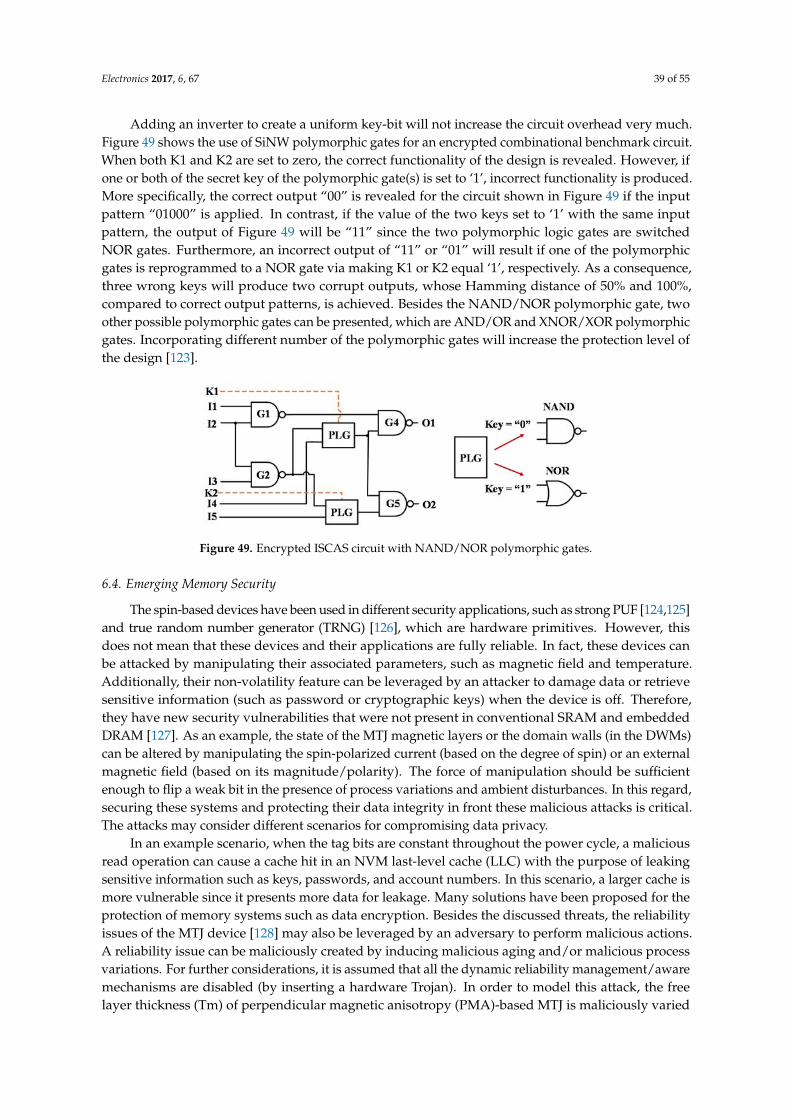
Electronics 2017, 6, 67 39 of 55
Adding an inverter to create a uniform key-bit will not increase the circuit overhead very much.Figure 49 shows the use of SiNW polymorphic gates for an encrypted combinational benchmark circuit.When both K1 and K2 are set to zero, the correct functionality of the design is revealed. However, ifone or both of the secret key of the polymorphic gate(s) is set to ‘1’, incorrect functionality is produced.More specifically, the correct output “00” is revealed for the circuit shown in Figure 49 if the inputpattern “01000” is applied. In contrast, if the value of the two keys set to ‘1’ with the same inputpattern, the output of Figure 49 will be “11” since the two polymorphic logic gates are switchedNOR gates. Furthermore, an incorrect output of “11” or “01” will result if one of the polymorphicgates is reprogrammed to a NOR gate via making K1 or K2 equal ‘1’, respectively. As a consequence,three wrong keys will produce two corrupt outputs, whose Hamming distance of 50% and 100%,compared to correct output patterns, is achieved. Besides the NAND/NOR polymorphic gate, twoother possible polymorphic gates can be presented, which are AND/OR and XNOR/XOR polymorphicgates. Incorporating different number of the polymorphic gates will increase the protection level ofthe design [123].
Electronics 2017, 6, 67 38 of 54
significantly if a designer replaces some of the gates in the original circuit with polymorphic gates
designed using SiNW FETs, instead of adding additional key‐gates, e.g., XOR/XNOR or AND/OR
gates or multiplexer. Moreover, in all of the previous works, there is only one key‐bit for each key‐
gate insertion. To successfully prevent attackers from using the brute force search, the secret key
length of the encrypted design should be large enough, e.g., larger than 128 bits. Increasing the size
of the secret key leads to increase the overhead largely, which might be larger than the size of the
original netlist. Interestingly, using SiNW polymorphic gates, the designer can enlarge the key size
up to 6x for any simple 2‐input gate if the keys are not gathered in a line for each exchanged gate.
Adding an inverter to create a uniform key‐bit will not increase the circuit overhead very much.
Figure 49 shows the use of SiNW polymorphic gates for an encrypted combinational benchmark
circuit. When both K1 and K2 are set to zero, the correct functionality of the design is revealed.
However, if one or both of the secret key of the polymorphic gate(s) is set to ‘1’, incorrect functionality
is produced. More specifically, the correct output “00” is revealed for the circuit shown in Figure 49
if the input pattern “01000” is applied. In contrast, if the value of the two keys set to ‘1’ with the same
input pattern, the output of Figure 49 will be “11” since the two polymorphic logic gates are switched
NOR gates. Furthermore, an incorrect output of “11” or “01” will result if one of the polymorphic
gates is reprogrammed to a NOR gate via making K1 or K2 equal ‘1’, respectively. As a consequence,
three wrong keys will produce two corrupt outputs, whose Hamming distance of 50% and 100%,
compared to correct output patterns, is achieved. Besides the NAND/NOR polymorphic gate, two
other possible polymorphic gates can be presented, which are AND/OR and XNOR/XOR
polymorphic gates. Incorporating different number of the polymorphic gates will increase the
protection level of the design [123].
Figure 49. Encrypted ISCAS circuit with NAND/NOR polymorphic gates.
6.4. Emerging Memory Security
The spin‐based devices have been used in different security applications, such as strong PUF
[124,125] and true random number generator (TRNG) [126], which are hardware primitives. However,
this does not mean that these devices and their applications are fully reliable. In fact, these devices
can be attacked by manipulating their associated parameters, such as magnetic field and temperature.
Additionally, their non‐volatility feature can be leveraged by an attacker to damage data or retrieve
sensitive information (such as password or cryptographic keys) when the device is off. Therefore,
they have new security vulnerabilities that were not present in conventional SRAM and embedded
DRAM [127]. As an example, the state of the MTJ magnetic layers or the domain walls (in the DWMs)
can be altered by manipulating the spin‐polarized current (based on the degree of spin) or an external
magnetic field (based on its magnitude/polarity). The force of manipulation should be sufficient
enough to flip a weak bit in the presence of process variations and ambient disturbances. In this
regard, securing these systems and protecting their data integrity in front these malicious attacks is
critical. The attacks may consider different scenarios for compromising data privacy.
In an example scenario, when the tag bits are constant throughout the power cycle, a malicious
read operation can cause a cache hit in an NVM last‐level cache (LLC) with the purpose of leaking
sensitive information such as keys, passwords, and account numbers. In this scenario, a larger cache
is more vulnerable since it presents more data for leakage. Many solutions have been proposed for
the protection of memory systems such as data encryption. Besides the discussed threats, the
Figure 49. Encrypted ISCAS circuit with NAND/NOR polymorphic gates.
6.4. Emerging Memory Security
The spin-based devices have been used in different security applications, such as strong PUF [124,125]and true random number generator (TRNG) [126], which are hardware primitives. However, thisdoes not mean that these devices and their applications are fully reliable. In fact, these devices canbe attacked by manipulating their associated parameters, such as magnetic field and temperature.Additionally, their non-volatility feature can be leveraged by an attacker to damage data or retrievesensitive information (such as password or cryptographic keys) when the device is off. Therefore,they have new security vulnerabilities that were not present in conventional SRAM and embeddedDRAM [127]. As an example, the state of the MTJ magnetic layers or the domain walls (in the DWMs)can be altered by manipulating the spin-polarized current (based on the degree of spin) or an externalmagnetic field (based on its magnitude/polarity). The force of manipulation should be sufficientenough to flip a weak bit in the presence of process variations and ambient disturbances. In this regard,securing these systems and protecting their data integrity in front these malicious attacks is critical.The attacks may consider different scenarios for compromising data privacy.
In an example scenario, when the tag bits are constant throughout the power cycle, a maliciousread operation can cause a cache hit in an NVM last-level cache (LLC) with the purpose of leakingsensitive information such as keys, passwords, and account numbers. In this scenario, a larger cache ismore vulnerable since it presents more data for leakage. Many solutions have been proposed for theprotection of memory systems such as data encryption. Besides the discussed threats, the reliabilityissues of the MTJ device [128] may also be leveraged by an adversary to perform malicious actions.A reliability issue can be maliciously created by inducing malicious aging and/or malicious processvariations. For further considerations, it is assumed that all the dynamic reliability management/awaremechanisms are disabled (by inserting a hardware Trojan). In order to model this attack, the freelayer thickness (Tm) of perpendicular magnetic anisotropy (PMA)-based MTJ is maliciously varied
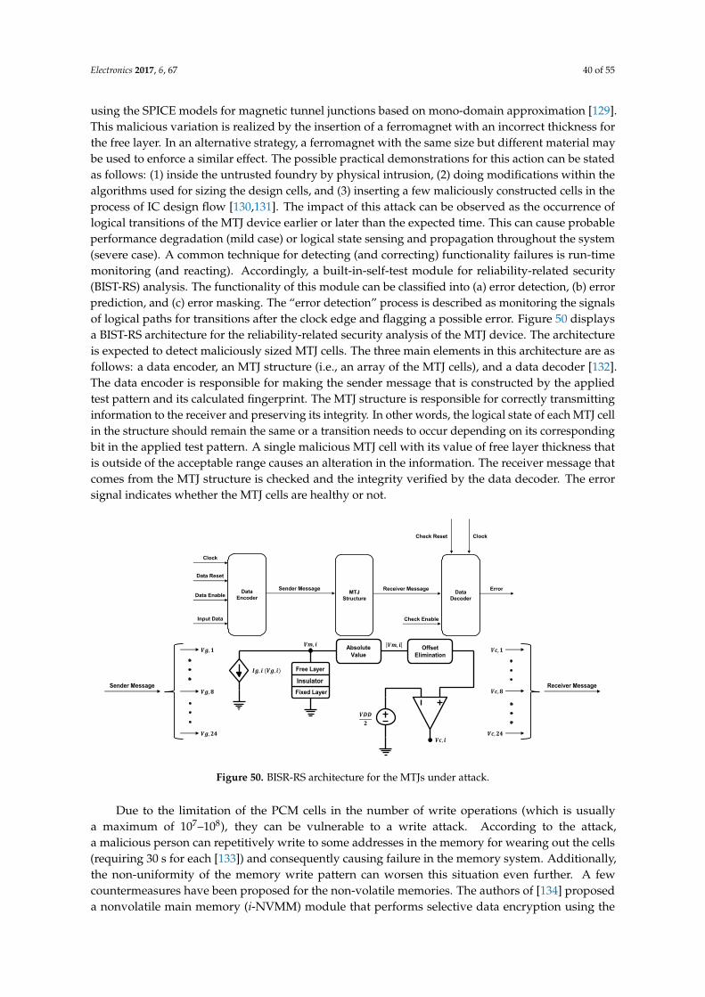
Electronics 2017, 6, 67 40 of 55
using the SPICE models for magnetic tunnel junctions based on mono-domain approximation [129].This malicious variation is realized by the insertion of a ferromagnet with an incorrect thickness forthe free layer. In an alternative strategy, a ferromagnet with the same size but different material maybe used to enforce a similar effect. The possible practical demonstrations for this action can be statedas follows: (1) inside the untrusted foundry by physical intrusion, (2) doing modifications within thealgorithms used for sizing the design cells, and (3) inserting a few maliciously constructed cells in theprocess of IC design flow [130,131]. The impact of this attack can be observed as the occurrence oflogical transitions of the MTJ device earlier or later than the expected time. This can cause probableperformance degradation (mild case) or logical state sensing and propagation throughout the system(severe case). A common technique for detecting (and correcting) functionality failures is run-timemonitoring (and reacting). Accordingly, a built-in-self-test module for reliability-related security(BIST-RS) analysis. The functionality of this module can be classified into (a) error detection, (b) errorprediction, and (c) error masking. The “error detection” process is described as monitoring the signalsof logical paths for transitions after the clock edge and flagging a possible error. Figure 50 displaysa BIST-RS architecture for the reliability-related security analysis of the MTJ device. The architectureis expected to detect maliciously sized MTJ cells. The three main elements in this architecture are asfollows: a data encoder, an MTJ structure (i.e., an array of the MTJ cells), and a data decoder [132].The data encoder is responsible for making the sender message that is constructed by the appliedtest pattern and its calculated fingerprint. The MTJ structure is responsible for correctly transmittinginformation to the receiver and preserving its integrity. In other words, the logical state of each MTJ cellin the structure should remain the same or a transition needs to occur depending on its correspondingbit in the applied test pattern. A single malicious MTJ cell with its value of free layer thickness thatis outside of the acceptable range causes an alteration in the information. The receiver message thatcomes from the MTJ structure is checked and the integrity verified by the data decoder. The errorsignal indicates whether the MTJ cells are healthy or not.
Electronics 2017, 6, 67 39 of 54
reliability issues of the MTJ device [128] may also be leveraged by an adversary to perform malicious
actions. A reliability issue can be maliciously created by inducing malicious aging and/or malicious
process variations. For further considerations, it is assumed that all the dynamic reliability
management/aware mechanisms are disabled (by inserting a hardware Trojan). In order to model
this attack, the free layer thickness (Tm) of perpendicular magnetic anisotropy (PMA)‐based MTJ is
maliciously varied using the SPICE models for magnetic tunnel junctions based on mono‐domain
approximation [129]. This malicious variation is realized by the insertion of a ferromagnet with an
incorrect thickness for the free layer. In an alternative strategy, a ferromagnet with the same size but
different material may be used to enforce a similar effect. The possible practical demonstrations for
this action can be stated as follows: (1) inside the untrusted foundry by physical intrusion, (2) doing
modifications within the algorithms used for sizing the design cells, and (3) inserting a few
maliciously constructed cells in the process of IC design flow [130,131]. The impact of this attack can
be observed as the occurrence of logical transitions of the MTJ device earlier or later than the expected
time. This can cause probable performance degradation (mild case) or logical state sensing and
propagation throughout the system (severe case). A common technique for detecting (and correcting)
functionality failures is run‐time monitoring (and reacting). Accordingly, a built‐in‐self‐test module
for reliability‐related security (BIST‐RS) analysis. The functionality of this module can be classified
into (a) error detection, (b) error prediction, and (c) error masking. The “error detection” process is
described as monitoring the signals of logical paths for transitions after the clock edge and flagging
a possible error. Figure 50 displays a BIST‐RS architecture for the reliability‐related security analysis
of the MTJ device. The architecture is expected to detect maliciously sized MTJ cells. The three main
elements in this architecture are as follows: a data encoder, an MTJ structure (i.e., an array of the MTJ
cells), and a data decoder [132]. The data encoder is responsible for making the sender message that
is constructed by the applied test pattern and its calculated fingerprint. The MTJ structure is
responsible for correctly transmitting information to the receiver and preserving its integrity. In other
words, the logical state of each MTJ cell in the structure should remain the same or a transition needs
to occur depending on its corresponding bit in the applied test pattern. A single malicious MTJ cell
with its value of free layer thickness that is outside of the acceptable range causes an alteration in the
information. The receiver message that comes from the MTJ structure is checked and the integrity
verified by the data decoder. The error signal indicates whether the MTJ cells are healthy or not.
Figure 50. BISR‐RS architecture for the MTJs under attack.
Due to the limitation of the PCM cells in the number of write operations (which is usually a
maximum of 107–108), they can be vulnerable to a write attack. According to the attack, a malicious
person can repetitively write to some addresses in the memory for wearing out the cells (requiring
30 s for each [133]) and consequently causing failure in the memory system. Additionally, the non‐
Figure 50. BISR-RS architecture for the MTJs under attack.
Due to the limitation of the PCM cells in the number of write operations (which is usuallya maximum of 107–108), they can be vulnerable to a write attack. According to the attack,a malicious person can repetitively write to some addresses in the memory for wearing out the cells(requiring 30 s for each [133]) and consequently causing failure in the memory system. Additionally,the non-uniformity of the memory write pattern can worsen this situation even further. A fewcountermeasures have been proposed for the non-volatile memories. The authors of [134] proposeda nonvolatile main memory (i-NVMM) module that performs selective data encryption using the
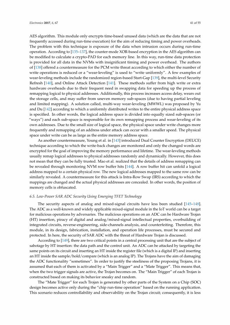
Electronics 2017, 6, 67 41 of 55
AES algorithm. This module only encrypts time-based unused data (which are the data that are notfrequently accessed during run-time execution) for the aim of reducing timing and power overheads.The problem with this technique is exposure of the data when intrusion occurs during run-timeoperation. According to [135–137], the counter-mode XOR-based encryption in the AES algorithm canbe modified to calculate a crypto-PAD for each memory line. In this way, run-time data protectionis provided for all data in the NVMs with insignificant timing and power overhead. The authorsof [138] offered a countermeasure for the PCM write threat according to which either the number ofwrite operations is reduced or a “wear-leveling” is used to “write uniformly”. A few examples ofwear-leveling methods include the randomized region-based Start-Gap [139], the multi-level SecurityRefresh [140], and Online Attack Detection [141]. These methods suffer from high write or extrahardware overheads due to their frequent need in swapping data for speeding up the process ofremapping logical to physical addresses. Additionally, this process increases access delay, wears outthe storage cells, and may suffer from uneven memory sub-spaces (due to having partial levelingand limited mapping). A solution called, multi-way wear-leveling (MWWL) was proposed by Yuand Du [142] according to which a uniformly distributed writes to the entire physical address spaceis specified. In other words, the logical address space is divided into equally sized sub-spaces (or“ways”) and each sub-space is responsible for its own remapping process and wear-leveling of itsown addresses. Due to the small size of logical space, the physical space under write changes morefrequently and remapping of an address under attack can occur with a smaller speed. The physicalspace under write can be as large as the entire memory address space.
As another countermeasure, Young et al. in [143] introduced Dual Counter Encryption (DEUCE)technique according to which the write-back changes are monitored and only the changed words areencrypted for the goal of improving the memory performance and lifetime. The wear-leveling methodsusually remap logical addresses to physical addresses randomly and dynamically. However, this doesnot mean that they can be fully trusted. Mao et al. realized that the details of address remapping canbe revealed through monitoring NVM row buffer hits [144]. A row buffer hit can unfold a logicaladdress mapped to a certain physical row. The new logical addresses mapped to the same row can besimilarly revealed. A countermeasure for this attack is Intra-Row Swap (IRS) according to which themappings are changed and the actual physical addresses are concealed. In other words, the position ofmemory cells is obfuscated.
6.5. Low-Power SAR ADC Security Using Emerging TFET Technology
The security aspects of analog and mixed-signal circuits have less been studied [145–148].The ADC as a well-known and widely applicable mixed-signal module in the IoT world can be a targetfor malicious operations by adversaries. The malicious operations on an ADC can be Hardware Trojan(HT) insertion, piracy of digital and analog/mixed-signal intellectual properties, overbuilding ofintegrated circuits, reverse-engineering, side-channels analysis, and counterfeiting. Therefore, thismodule, in its design, fabrication, installation, and operation life processes, must be secured andprotected. In here, the security of SAR ADC with the threat of Hardware Trojan is discussed.
According to [149], there are two critical points in a central processing unit that are the subject ofsabotage by HT insertion: the data path and the control unit. An ADC can be attacked by targeting thesame points on its circuit and inserting an HT inside the register file (which is a digital IP) and insertingan HT inside the sample/hold/compare (which is an analog IP). The Trojans have the aim of damagingthe ADC functionality “sometimes”. In order to justify the steeliness of the proposing Trojans, it isassumed that each of them is activated by a “Main Trigger” and a “Mate Trigger”. This means that,when the two trigger signals are active, the Trojan becomes on. The “Main Trigger” of each Trojan isconstructed based on making its behavior sneaky and random.
The “Mate Trigger” for each Trojan is generated by other parts of the System on a Chip (SOC)design becomes active only during the “chip run-time operation” based on the running application.This scenario reduces controllability and observability on the Trojan circuit; consequently, it is less
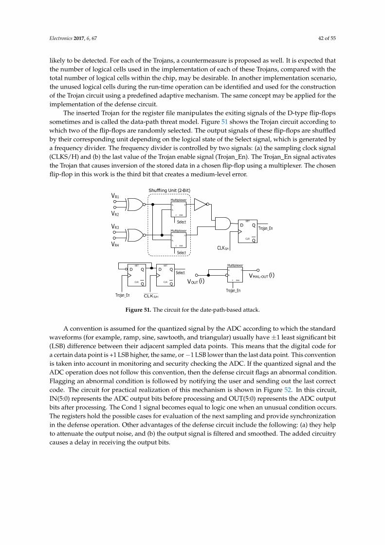
Electronics 2017, 6, 67 42 of 55
likely to be detected. For each of the Trojans, a countermeasure is proposed as well. It is expected thatthe number of logical cells used in the implementation of each of these Trojans, compared with thetotal number of logical cells within the chip, may be desirable. In another implementation scenario,the unused logical cells during the run-time operation can be identified and used for the constructionof the Trojan circuit using a predefined adaptive mechanism. The same concept may be applied for theimplementation of the defense circuit.
The inserted Trojan for the register file manipulates the exiting signals of the D-type flip-flopssometimes and is called the data-path threat model. Figure 51 shows the Trojan circuit according towhich two of the flip-flops are randomly selected. The output signals of these flip-flops are shuffledby their corresponding unit depending on the logical state of the Select signal, which is generated bya frequency divider. The frequency divider is controlled by two signals: (a) the sampling clock signal(CLKS/H) and (b) the last value of the Trojan enable signal (Trojan_En). The Trojan_En signal activatesthe Trojan that causes inversion of the stored data in a chosen flip-flop using a multiplexer. The chosenflip-flop in this work is the third bit that creates a medium-level error.
Electronics 2017, 6, 67 41 of 54
This scenario reduces controllability and observability on the Trojan circuit; consequently, it is less
likely to be detected. For each of the Trojans, a countermeasure is proposed as well. It is expected that
the number of logical cells used in the implementation of each of these Trojans, compared with the
total number of logical cells within the chip, may be desirable. In another implementation scenario,
the unused logical cells during the run‐time operation can be identified and used for the construction
of the Trojan circuit using a predefined adaptive mechanism. The same concept may be applied for
the implementation of the defense circuit.
The inserted Trojan for the register file manipulates the exiting signals of the D‐type flip‐flops
sometimes and is called the data‐path threat model. Figure 51 shows the Trojan circuit according to
which two of the flip‐flops are randomly selected. The output signals of these flip‐flops are shuffled
by their corresponding unit depending on the logical state of the Select signal, which is generated by
a frequency divider. The frequency divider is controlled by two signals: (a) the sampling clock signal
(CLKS/H) and (b) the last value of the Trojan enable signal (Trojan_En). The Trojan_En signal
activates the Trojan that causes inversion of the stored data in a chosen flip‐flop using a multiplexer.
The chosen flip‐flop in this work is the third bit that creates a medium‐level error.
Figure 51. The circuit for the date‐path‐based attack.
A convention is assumed for the quantized signal by the ADC according to which the standard
waveforms (for example, ramp, sine, sawtooth, and triangular) usually have ±1 least significant bit
(LSB) difference between their adjacent sampled data points. This means that the digital code for a
certain data point is +1 LSB higher, the same, or −1 LSB lower than the last data point. This convention
is taken into account in monitoring and security checking the ADC. If the quantized signal and the
ADC operation does not follow this convention, then the defense circuit flags an abnormal condition.
Flagging an abnormal condition is followed by notifying the user and sending out the last correct
code. The circuit for practical realization of this mechanism is shown in Figure 52. In this circuit,
IN(5:0) represents the ADC output bits before processing and OUT(5:0) represents the ADC output
bits after processing. The Cond 1 signal becomes equal to logic one when an unusual condition occurs.
The registers hold the possible cases for evaluation of the next sampling and provide synchronization
in the defense operation. Other advantages of the defense circuit include the following: (a) they help
to attenuate the output noise, and (b) the output signal is filtered and smoothed. The added circuitry
causes a delay in receiving the output bits.
Figure 51. The circuit for the date-path-based attack.
A convention is assumed for the quantized signal by the ADC according to which the standardwaveforms (for example, ramp, sine, sawtooth, and triangular) usually have ±1 least significant bit(LSB) difference between their adjacent sampled data points. This means that the digital code fora certain data point is +1 LSB higher, the same, or−1 LSB lower than the last data point. This conventionis taken into account in monitoring and security checking the ADC. If the quantized signal and theADC operation does not follow this convention, then the defense circuit flags an abnormal condition.Flagging an abnormal condition is followed by notifying the user and sending out the last correctcode. The circuit for practical realization of this mechanism is shown in Figure 52. In this circuit,IN(5:0) represents the ADC output bits before processing and OUT(5:0) represents the ADC outputbits after processing. The Cond 1 signal becomes equal to logic one when an unusual condition occurs.The registers hold the possible cases for evaluation of the next sampling and provide synchronizationin the defense operation. Other advantages of the defense circuit include the following: (a) they helpto attenuate the output noise, and (b) the output signal is filtered and smoothed. The added circuitrycauses a delay in receiving the output bits.
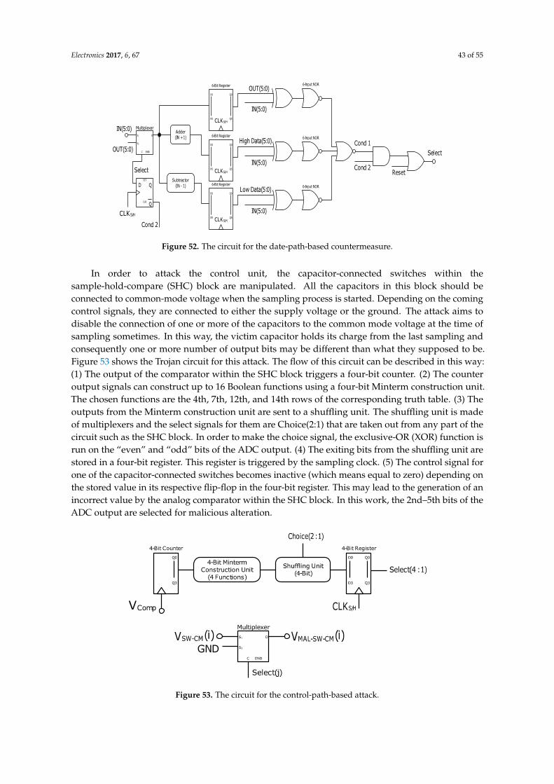
Electronics 2017, 6, 67 43 of 55Electronics 2017, 6, 67 42 of 54
Figure 52. The circuit for the date‐path‐based countermeasure.
In order to attack the control unit, the capacitor‐connected switches within the sample‐hold‐
compare (SHC) block are manipulated. All the capacitors in this block should be connected to
common‐mode voltage when the sampling process is started. Depending on the coming control
signals, they are connected to either the supply voltage or the ground. The attack aims to disable the
connection of one or more of the capacitors to the common mode voltage at the time of sampling
sometimes. In this way, the victim capacitor holds its charge from the last sampling and consequently
one or more number of output bits may be different than what they supposed to be. Figure 53 shows
the Trojan circuit for this attack. The flow of this circuit can be described in this way: (1) The output
of the comparator within the SHC block triggers a four‐bit counter. (2) The counter output signals
can construct up to 16 Boolean functions using a four‐bit Minterm construction unit. The chosen
functions are the 4th, 7th, 12th, and 14th rows of the corresponding truth table. (3) The outputs from
the Minterm construction unit are sent to a shuffling unit. The shuffling unit is made of multiplexers
and the select signals for them are Choice(2:1) that are taken out from any part of the circuit such as
the SHC block. In order to make the choice signal, the exclusive‐OR (XOR) function is run on the
“even” and “odd” bits of the ADC output. (4) The exiting bits from the shuffling unit are stored in a
four‐bit register. This register is triggered by the sampling clock. (5) The control signal for one of the
capacitor‐connected switches becomes inactive (which means equal to zero) depending on the stored
value in its respective flip‐flop in the four‐bit register. This may lead to the generation of an incorrect
value by the analog comparator within the SHC block. In this work, the 2nd–5th bits of the ADC
output are selected for malicious alteration.
Figure 53. The circuit for the control‐path‐based attack.
A common technique in designing a Built‐in‐Self‐Test (BIST) module for an IC is “sub‐circuit
replication” [150]. A BIST module can be externally inserted or internally developed (from the
available design cells in a certain chip mode). Here, the countermeasure for the control‐based threat
Figure 52. The circuit for the date-path-based countermeasure.
In order to attack the control unit, the capacitor-connected switches within thesample-hold-compare (SHC) block are manipulated. All the capacitors in this block should beconnected to common-mode voltage when the sampling process is started. Depending on the comingcontrol signals, they are connected to either the supply voltage or the ground. The attack aims todisable the connection of one or more of the capacitors to the common mode voltage at the time ofsampling sometimes. In this way, the victim capacitor holds its charge from the last sampling andconsequently one or more number of output bits may be different than what they supposed to be.Figure 53 shows the Trojan circuit for this attack. The flow of this circuit can be described in this way:(1) The output of the comparator within the SHC block triggers a four-bit counter. (2) The counteroutput signals can construct up to 16 Boolean functions using a four-bit Minterm construction unit.The chosen functions are the 4th, 7th, 12th, and 14th rows of the corresponding truth table. (3) Theoutputs from the Minterm construction unit are sent to a shuffling unit. The shuffling unit is madeof multiplexers and the select signals for them are Choice(2:1) that are taken out from any part of thecircuit such as the SHC block. In order to make the choice signal, the exclusive-OR (XOR) function isrun on the “even” and “odd” bits of the ADC output. (4) The exiting bits from the shuffling unit arestored in a four-bit register. This register is triggered by the sampling clock. (5) The control signal forone of the capacitor-connected switches becomes inactive (which means equal to zero) depending onthe stored value in its respective flip-flop in the four-bit register. This may lead to the generation of anincorrect value by the analog comparator within the SHC block. In this work, the 2nd–5th bits of theADC output are selected for malicious alteration.
Electronics 2017, 6, 67 42 of 54
Figure 52. The circuit for the date‐path‐based countermeasure.
In order to attack the control unit, the capacitor‐connected switches within the sample‐hold‐
compare (SHC) block are manipulated. All the capacitors in this block should be connected to
common‐mode voltage when the sampling process is started. Depending on the coming control
signals, they are connected to either the supply voltage or the ground. The attack aims to disable the
connection of one or more of the capacitors to the common mode voltage at the time of sampling
sometimes. In this way, the victim capacitor holds its charge from the last sampling and consequently
one or more number of output bits may be different than what they supposed to be. Figure 53 shows
the Trojan circuit for this attack. The flow of this circuit can be described in this way: (1) The output
of the comparator within the SHC block triggers a four‐bit counter. (2) The counter output signals
can construct up to 16 Boolean functions using a four‐bit Minterm construction unit. The chosen
functions are the 4th, 7th, 12th, and 14th rows of the corresponding truth table. (3) The outputs from
the Minterm construction unit are sent to a shuffling unit. The shuffling unit is made of multiplexers
and the select signals for them are Choice(2:1) that are taken out from any part of the circuit such as
the SHC block. In order to make the choice signal, the exclusive‐OR (XOR) function is run on the
“even” and “odd” bits of the ADC output. (4) The exiting bits from the shuffling unit are stored in a
four‐bit register. This register is triggered by the sampling clock. (5) The control signal for one of the
capacitor‐connected switches becomes inactive (which means equal to zero) depending on the stored
value in its respective flip‐flop in the four‐bit register. This may lead to the generation of an incorrect
value by the analog comparator within the SHC block. In this work, the 2nd–5th bits of the ADC
output are selected for malicious alteration.
Figure 53. The circuit for the control‐path‐based attack.
A common technique in designing a Built‐in‐Self‐Test (BIST) module for an IC is “sub‐circuit
replication” [150]. A BIST module can be externally inserted or internally developed (from the
available design cells in a certain chip mode). Here, the countermeasure for the control‐based threat
Figure 53. The circuit for the control-path-based attack.
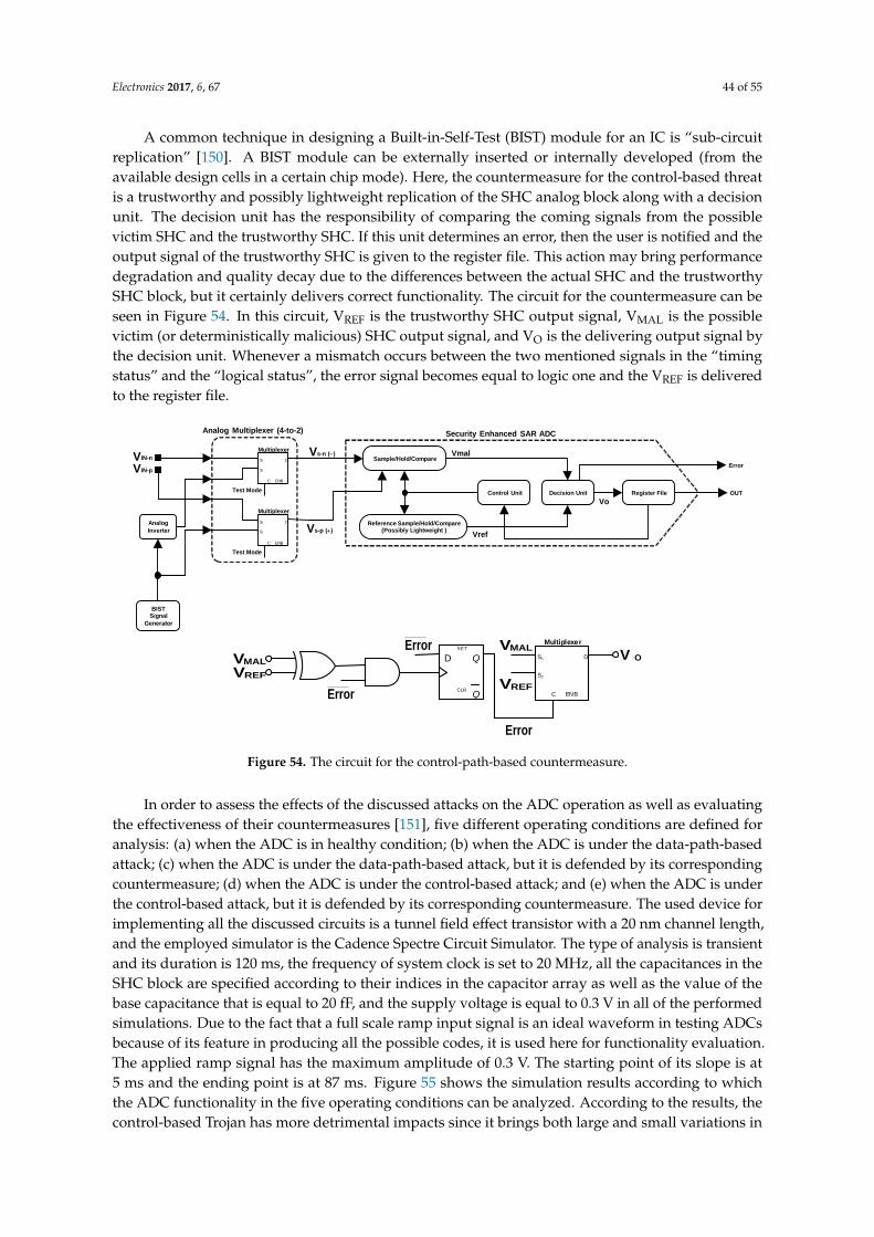
Electronics 2017, 6, 67 44 of 55
A common technique in designing a Built-in-Self-Test (BIST) module for an IC is “sub-circuitreplication” [150]. A BIST module can be externally inserted or internally developed (from theavailable design cells in a certain chip mode). Here, the countermeasure for the control-based threatis a trustworthy and possibly lightweight replication of the SHC analog block along with a decisionunit. The decision unit has the responsibility of comparing the coming signals from the possiblevictim SHC and the trustworthy SHC. If this unit determines an error, then the user is notified and theoutput signal of the trustworthy SHC is given to the register file. This action may bring performancedegradation and quality decay due to the differences between the actual SHC and the trustworthySHC block, but it certainly delivers correct functionality. The circuit for the countermeasure can beseen in Figure 54. In this circuit, VREF is the trustworthy SHC output signal, VMAL is the possiblevictim (or deterministically malicious) SHC output signal, and VO is the delivering output signal bythe decision unit. Whenever a mismatch occurs between the two mentioned signals in the “timingstatus” and the “logical status”, the error signal becomes equal to logic one and the VREF is deliveredto the register file.
Electronics 2017, 6, 67 43 of 54
is a trustworthy and possibly lightweight replication of the SHC analog block along with a decision
unit. The decision unit has the responsibility of comparing the coming signals from the possible
victim SHC and the trustworthy SHC. If this unit determines an error, then the user is notified and
the output signal of the trustworthy SHC is given to the register file. This action may bring
performance degradation and quality decay due to the differences between the actual SHC and the
trustworthy SHC block, but it certainly delivers correct functionality. The circuit for the
countermeasure can be seen in Figure 54. In this circuit, VREF is the trustworthy SHC output signal,
VMAL is the possible victim (or deterministically malicious) SHC output signal, and VO is the
delivering output signal by the decision unit. Whenever a mismatch occurs between the two
mentioned signals in the “timing status” and the “logical status”, the error signal becomes equal to
logic one and the VREF is delivered to the register file.
Figure 54. The circuit for the control‐path‐based countermeasure.
In order to assess the effects of the discussed attacks on the ADC operation as well as evaluating
the effectiveness of their countermeasures [151], five different operating conditions are defined for
analysis: (a) when the ADC is in healthy condition; (b) when the ADC is under the data‐path‐based
attack; (c) when the ADC is under the data‐path‐based attack, but it is defended by its corresponding
countermeasure; (d) when the ADC is under the control‐based attack; and (e) when the ADC is under
the control‐based attack, but it is defended by its corresponding countermeasure. The used device for
implementing all the discussed circuits is a tunnel field effect transistor with a 20 nm channel length,
and the employed simulator is the Cadence Spectre Circuit Simulator. The type of analysis is transient
and its duration is 120 ms, the frequency of system clock is set to 20 MHz, all the capacitances in the
SHC block are specified according to their indices in the capacitor array as well as the value of the
base capacitance that is equal to 20 fF, and the supply voltage is equal to 0.3 V in all of the performed
simulations. Due to the fact that a full scale ramp input signal is an ideal waveform in testing ADCs
because of its feature in producing all the possible codes, it is used here for functionality evaluation.
The applied ramp signal has the maximum amplitude of 0.3 V. The starting point of its slope is at 5
ms and the ending point is at 87 ms. Figure 55 shows the simulation results according to which the
ADC functionality in the five operating conditions can be analyzed. According to the results, the
control‐based Trojan has more detrimental impacts since it brings both large and small variations in
the reconstructed analog signal from the ADC output, while the data‐path‐based Trojan causes only
a few large variations. The capability of the countermeasures in eliminating the impacts of attacks is
acceptable.
Sample/Hold/Compare
Register FileControl Unit OUT
Reference Sample/Hold/Compare(Possibly Lightweight )
Decision Unit
Error
Vo
Vref
Vmal
Security Enhanced SAR ADC
Analog Inverter
BIST Signal
Generator
S1
S2
D
C ENB
Multiplexer
S1
S2
D
C ENB
Multiplexer
Analog Multiplexer (4-to-2)
VIN-n
VIN-p
Test Mode
Test Mode
Vs-n ()
Vs-p ()
VREF
VMAL
Q
QSET
CLR
D S1
S2
D
C ENB
Multiplexer
Error
Error
Error
VREF
VMALV O
Figure 54. The circuit for the control-path-based countermeasure.
In order to assess the effects of the discussed attacks on the ADC operation as well as evaluatingthe effectiveness of their countermeasures [151], five different operating conditions are defined foranalysis: (a) when the ADC is in healthy condition; (b) when the ADC is under the data-path-basedattack; (c) when the ADC is under the data-path-based attack, but it is defended by its correspondingcountermeasure; (d) when the ADC is under the control-based attack; and (e) when the ADC is underthe control-based attack, but it is defended by its corresponding countermeasure. The used device forimplementing all the discussed circuits is a tunnel field effect transistor with a 20 nm channel length,and the employed simulator is the Cadence Spectre Circuit Simulator. The type of analysis is transientand its duration is 120 ms, the frequency of system clock is set to 20 MHz, all the capacitances in theSHC block are specified according to their indices in the capacitor array as well as the value of thebase capacitance that is equal to 20 fF, and the supply voltage is equal to 0.3 V in all of the performedsimulations. Due to the fact that a full scale ramp input signal is an ideal waveform in testing ADCsbecause of its feature in producing all the possible codes, it is used here for functionality evaluation.The applied ramp signal has the maximum amplitude of 0.3 V. The starting point of its slope is at5 ms and the ending point is at 87 ms. Figure 55 shows the simulation results according to whichthe ADC functionality in the five operating conditions can be analyzed. According to the results, thecontrol-based Trojan has more detrimental impacts since it brings both large and small variations in
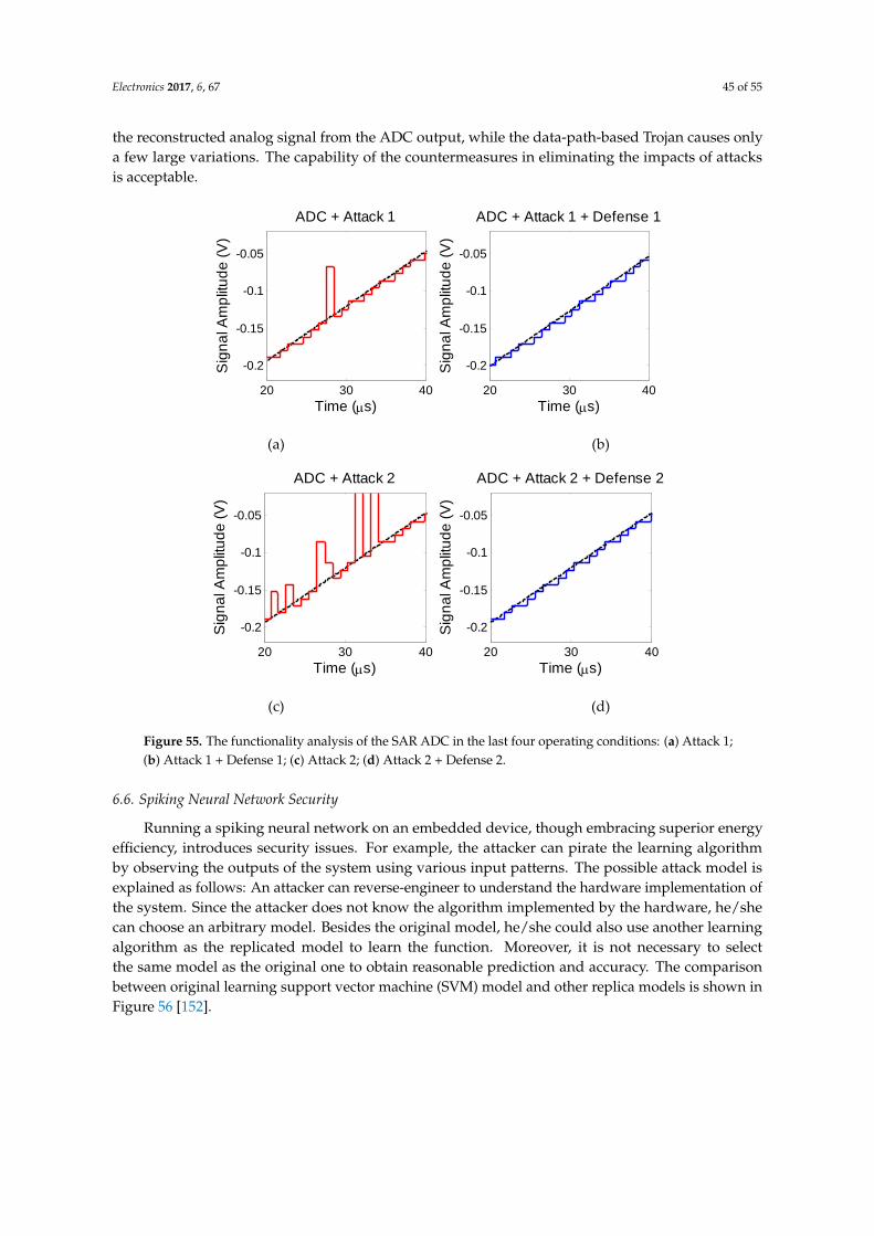
Electronics 2017, 6, 67 45 of 55
the reconstructed analog signal from the ADC output, while the data-path-based Trojan causes onlya few large variations. The capability of the countermeasures in eliminating the impacts of attacksis acceptable.Electronics 2017, 6, 67 44 of 54
(a) (b)
(c) (d)
Figure 55. The functionality analysis of the SAR ADC in the last four operating conditions: (a) Attack
1; (b) Attack 1 + Defense 1; (c) Attack 2; (d) Attack 2 + Defense 2.
6.6. Spiking Neural Network Security
Running a spiking neural network on an embedded device, though embracing superior energy
efficiency, introduces security issues. For example, the attacker can pirate the learning algorithm by
observing the outputs of the system using various input patterns. The possible attack model is
explained as follows: An attacker can reverse‐engineer to understand the hardware implementation
of the system. Since the attacker does not know the algorithm implemented by the hardware, he/she
can choose an arbitrary model. Besides the original model, he/she could also use another learning
algorithm as the replicated model to learn the function. Moreover, it is not necessary to select the
same model as the original one to obtain reasonable prediction and accuracy. The comparison
between original learning support vector machine (SVM) model and other replica models is shown
in Figure 56 [152].
20 30 40
-0.2
-0.15
-0.1
-0.05
Sig
na
l Am
plit
ud
e (
V)
Time (s)
ADC + Attack 1
20 30 40
-0.2
-0.15
-0.1
-0.05
Sig
na
l Am
plit
ud
e (
V)
Time (s)
ADC + Attack 1 + Defense 1
20 30 40
-0.2
-0.15
-0.1
-0.05
Sig
na
l Am
plit
ud
e (
V)
Time (s)
ADC + Attack 2
20 30 40
-0.2
-0.15
-0.1
-0.05
Sig
na
l Am
plit
ud
e (
V)
Time (s)
ADC + Attack 2 + Defense 2
Figure 55. The functionality analysis of the SAR ADC in the last four operating conditions: (a) Attack 1;(b) Attack 1 + Defense 1; (c) Attack 2; (d) Attack 2 + Defense 2.
6.6. Spiking Neural Network Security
Running a spiking neural network on an embedded device, though embracing superior energyefficiency, introduces security issues. For example, the attacker can pirate the learning algorithmby observing the outputs of the system using various input patterns. The possible attack model isexplained as follows: An attacker can reverse-engineer to understand the hardware implementation ofthe system. Since the attacker does not know the algorithm implemented by the hardware, he/shecan choose an arbitrary model. Besides the original model, he/she could also use another learningalgorithm as the replicated model to learn the function. Moreover, it is not necessary to selectthe same model as the original one to obtain reasonable prediction and accuracy. The comparisonbetween original learning support vector machine (SVM) model and other replica models is shown inFigure 56 [152].
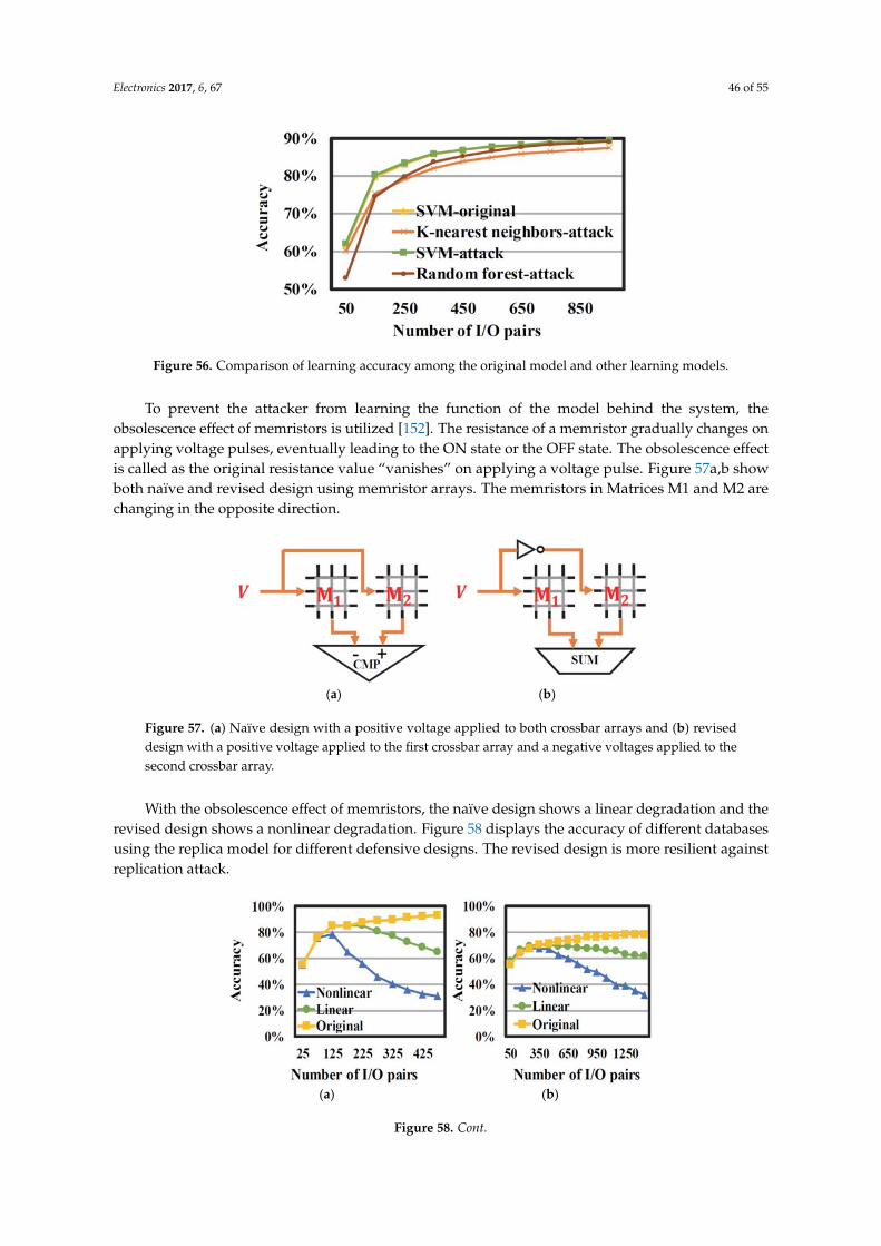
Electronics 2017, 6, 67 46 of 55Electronics 2017, 6, 67 45 of 54
Figure 56. Comparison of learning accuracy among the original model and other learning models.
To prevent the attacker from learning the function of the model behind the system, the
obsolescence effect of memristors is utilized [152]. The resistance of a memristor gradually changes
on applying voltage pulses, eventually leading to the ON state or the OFF state. The obsolescence
effect is called as the original resistance value “vanishes” on applying a voltage pulse. Figure 57a,b
show both naïve and revised design using memristor arrays. The memristors in Matrices M1 and M2
are changing in the opposite direction.
(a) (b)
Figure 57. (a) Naïve design with a positive voltage applied to both crossbar arrays and (b) revised
design with a positive voltage applied to the first crossbar array and a negative voltages applied to
the second crossbar array.
With the obsolescence effect of memristors, the naïve design shows a linear degradation and the
revised design shows a nonlinear degradation. Figure 58 displays the accuracy of different databases
using the replica model for different defensive designs. The revised design is more resilient against
replication attack.
(a) (b)
Figure 56. Comparison of learning accuracy among the original model and other learning models.
To prevent the attacker from learning the function of the model behind the system, theobsolescence effect of memristors is utilized [152]. The resistance of a memristor gradually changes onapplying voltage pulses, eventually leading to the ON state or the OFF state. The obsolescence effectis called as the original resistance value “vanishes” on applying a voltage pulse. Figure 57a,b showboth naïve and revised design using memristor arrays. The memristors in Matrices M1 and M2 arechanging in the opposite direction.
Electronics 2017, 6, 67 45 of 54
Figure 56. Comparison of learning accuracy among the original model and other learning models.
To prevent the attacker from learning the function of the model behind the system, the
obsolescence effect of memristors is utilized [152]. The resistance of a memristor gradually changes
on applying voltage pulses, eventually leading to the ON state or the OFF state. The obsolescence
effect is called as the original resistance value “vanishes” on applying a voltage pulse. Figure 57a,b
show both naïve and revised design using memristor arrays. The memristors in Matrices M1 and M2
are changing in the opposite direction.
(a) (b)
Figure 57. (a) Naïve design with a positive voltage applied to both crossbar arrays and (b) revised
design with a positive voltage applied to the first crossbar array and a negative voltages applied to
the second crossbar array.
With the obsolescence effect of memristors, the naïve design shows a linear degradation and the
revised design shows a nonlinear degradation. Figure 58 displays the accuracy of different databases
using the replica model for different defensive designs. The revised design is more resilient against
replication attack.
(a) (b)
Figure 57. (a) Naïve design with a positive voltage applied to both crossbar arrays and (b) reviseddesign with a positive voltage applied to the first crossbar array and a negative voltages applied to thesecond crossbar array.
With the obsolescence effect of memristors, the naïve design shows a linear degradation and therevised design shows a nonlinear degradation. Figure 58 displays the accuracy of different databasesusing the replica model for different defensive designs. The revised design is more resilient againstreplication attack.
Electronics 2017, 6, 67 45 of 54
Figure 56. Comparison of learning accuracy among the original model and other learning models.
To prevent the attacker from learning the function of the model behind the system, the
obsolescence effect of memristors is utilized [152]. The resistance of a memristor gradually changes
on applying voltage pulses, eventually leading to the ON state or the OFF state. The obsolescence
effect is called as the original resistance value “vanishes” on applying a voltage pulse. Figure 57a,b
show both naïve and revised design using memristor arrays. The memristors in Matrices M1 and M2
are changing in the opposite direction.
(a) (b)
Figure 57. (a) Naïve design with a positive voltage applied to both crossbar arrays and (b) revised
design with a positive voltage applied to the first crossbar array and a negative voltages applied to
the second crossbar array.
With the obsolescence effect of memristors, the naïve design shows a linear degradation and the
revised design shows a nonlinear degradation. Figure 58 displays the accuracy of different databases
using the replica model for different defensive designs. The revised design is more resilient against
replication attack.
(a) (b)
Figure 58. Cont.
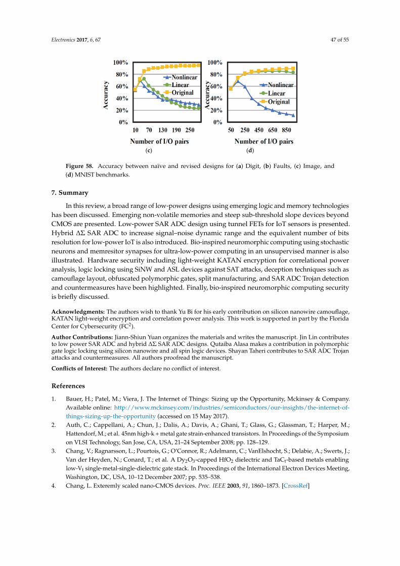
Electronics 2017, 6, 67 47 of 55
Electronics 2017, 6, 67 46 of 54
(c) (d)
Figure 58. Accuracy between naïve and revised designs for (a) Digit, (b) Faults, (c) Image, and (d)
MNIST benchmarks.
7. Summary
In this review, a broad range of low‐power designs using emerging logic and memory
technologies has been discussed. Emerging non‐volatile memories and steep sub‐threshold slope
devices beyond CMOS are presented. Low‐power SAR ADC design using tunnel FETs for IoT sensors
is presented. Hybrid Δ� SAR ADC to increase signal–noise dynamic range and the equivalent
number of bits resolution for low‐power IoT is also introduced. Bio‐inspired neuromorphic
computing using stochastic neurons and memresitor synapses for ultra‐low‐power computing in an
unsupervised manner is also illustrated. Hardware security including light‐weight KATAN
encryption for correlational power analysis, logic locking using SiNW and ASL devices against SAT
attacks, deception techniques such as camouflage layout, obfuscated polymorphic gates, split
manufacturing, and SAR ADC Trojan detection and countermeasures have been highlighted. Finally,
bio‐inspired neuromorphic computing security is briefly discussed.
Acknowledgments: The authors wish to thank Yu Bi for his early contribution on silicon nanowire camouflage,
KATAN light‐weight encryption and correlation power analysis. This work is supported in part by the Florida
Center for Cybersecurity (FC2).
Author Contributions: Jiann‐Shiun Yuan organizes the materials and writes the manuscript. Jin Lin contributes
to low power SAR ADC and hybrid ΔƩ SAR ADC designs. Qutaiba Alasa makes a contribution in polymorphic
gate logic locking using silicon nanowire and all spin logic devices. Shayan Taheri contributes to SAR ADC
Trojan attacks and countermeasures. All authors proofread the manuscript.
Conflicts of Interest: The authors declare no conflict of interest.
References
1. Bauer, H.; Patel, M.; Viera, J. The Internet of Things: Sizing up the Opportunity, Mckinsey & Company.
Available online: http://www.mckinsey.com/industries/semiconductors/our‐insights/the‐internet‐of‐
things‐sizing‐up‐the‐opportunity (accessed on 15 May 2017).
2. Auth, C.; Cappellani, A.; Chun, J.; Dalis, A.; Davis, A.; Ghani, T.; Glass, G.; Glassman, T.; Harper, M.;
Hattendorf, M.; et al. 45nm high‐k + metal gate strain‐enhanced transistors. In Proceedings of the
Symposium on VLSI Technology, San Jose, CA, USA, 21–24 September 2008; pp. 128–129.
3. Chang, V.; Ragnarsson, L.; Pourtois, G.; O’Connor, R.; Adelmann, C.; VanElshocht, S.; Delabie, A.; Swerts,
J.; Van der Heyden, N.; Conard, T.; et al. A Dy2O3‐capped HfO2 dielectric and TaCt‐based metals enabling
low‐Vt single‐metal‐single‐dielectric gate stack. In Proceedings of the International Electron Devices
Meeting, Washington, DC, USA, 10–12 December 2007; pp. 535–538.
4. Chang, L. Exteremly scaled nano‐CMOS devices. Proc. IEEE 2003, 91, 1860–1873.
5. Wu, C.; Lin, D.; Keshavarzi, A.; Huang, C.; Chan, C.; Tseng, C.; Chen, C.; Hsieh, C.; Wong, K.; Cheng, M.;
et al. High performance 22/20nm FinFET CMOS devices with advanced high‐K/metal gate scheme. In
Figure 58. Accuracy between naïve and revised designs for (a) Digit, (b) Faults, (c) Image, and(d) MNIST benchmarks.
7. Summary
In this review, a broad range of low-power designs using emerging logic and memory technologieshas been discussed. Emerging non-volatile memories and steep sub-threshold slope devices beyondCMOS are presented. Low-power SAR ADC design using tunnel FETs for IoT sensors is presented.Hybrid ∆Σ SAR ADC to increase signal–noise dynamic range and the equivalent number of bitsresolution for low-power IoT is also introduced. Bio-inspired neuromorphic computing using stochasticneurons and memresitor synapses for ultra-low-power computing in an unsupervised manner is alsoillustrated. Hardware security including light-weight KATAN encryption for correlational poweranalysis, logic locking using SiNW and ASL devices against SAT attacks, deception techniques such ascamouflage layout, obfuscated polymorphic gates, split manufacturing, and SAR ADC Trojan detectionand countermeasures have been highlighted. Finally, bio-inspired neuromorphic computing securityis briefly discussed.
Acknowledgments: The authors wish to thank Yu Bi for his early contribution on silicon nanowire camouflage,KATAN light-weight encryption and correlation power analysis. This work is supported in part by the FloridaCenter for Cybersecurity (FC2).
Author Contributions: Jiann-Shiun Yuan organizes the materials and writes the manuscript. Jin Lin contributesto low power SAR ADC and hybrid ∆Σ SAR ADC designs. Qutaiba Alasa makes a contribution in polymorphicgate logic locking using silicon nanowire and all spin logic devices. Shayan Taheri contributes to SAR ADC Trojanattacks and countermeasures. All authors proofread the manuscript.
Conflicts of Interest: The authors declare no conflict of interest.
References
1. Bauer, H.; Patel, M.; Viera, J. The Internet of Things: Sizing up the Opportunity, Mckinsey & Company.Available online: http://www.mckinsey.com/industries/semiconductors/our-insights/the-internet-of-things-sizing-up-the-opportunity (accessed on 15 May 2017).
2. Auth, C.; Cappellani, A.; Chun, J.; Dalis, A.; Davis, A.; Ghani, T.; Glass, G.; Glassman, T.; Harper, M.;Hattendorf, M.; et al. 45nm high-k + metal gate strain-enhanced transistors. In Proceedings of the Symposiumon VLSI Technology, San Jose, CA, USA, 21–24 September 2008; pp. 128–129.
3. Chang, V.; Ragnarsson, L.; Pourtois, G.; O’Connor, R.; Adelmann, C.; VanElshocht, S.; Delabie, A.; Swerts, J.;Van der Heyden, N.; Conard, T.; et al. A Dy2O3-capped HfO2 dielectric and TaCt-based metals enablinglow-Vt single-metal-single-dielectric gate stack. In Proceedings of the International Electron Devices Meeting,Washington, DC, USA, 10–12 December 2007; pp. 535–538.
4. Chang, L. Exteremly scaled nano-CMOS devices. Proc. IEEE 2003, 91, 1860–1873. [CrossRef]
Electronics 2017, 6, 67 48 of 55
5. Wu, C.; Lin, D.; Keshavarzi, A.; Huang, C.; Chan, C.; Tseng, C.; Chen, C.; Hsieh, C.; Wong, K.; Cheng, M.; et al.High performance 22/20nm FinFET CMOS devices with advanced high-K/metal gate scheme. In Proceedingsof the 2010 International Electron Devices Meeting, San Francisco, CA, USA, 6–8 December 2010.
6. Seok, M.; Chen, G.; Hanson, S.; Wieckowski, M.; Blaauw, D.; Sylverster, D. CAS-FEST 2010: Mitigatingvariability in near-threshold computing. IEEE Trans. Emerg. Sel. Top. Circuits Syst. 2011, 1, 42–49. [CrossRef]
7. Farooq, M.G.; Graves-Abe, T.L.; Landers, W.F.; Kothandaraman, C.; Himmel, B.A.; Andry, P.S.; Tsang, C.K.;Sprogis, E.; Volant, R.P.; Petrarca, K.S. 3D copper TSV integration, testing and reliability. In Proceedings ofthe International Electron Devices Meeting, Washington, DC, USA, 5–7 December 2011.
8. Devadas, V.; Aydin, H. On the interplay of voltage/frequency scaling and device power management forframe-based real-time embedded applications. IEEE Trans. Comput. 2011, 61, 1–31. [CrossRef]
9. Dorsey, J.; Searles, S.; Ciraula, M.; Johnson, S.; Bujanos, N.; Wu, D.; Braganza, M.; Meyers, S.; Fang, E.;Kumar, R. An integrated quad-core opteron™ processor. In Proceedings of the International Solid-SateCircuits Conference, San Francisco, CA, USA, 11–15 February 2007; pp. 102–103.
10. Pakbaznia, E.; Pedram, M. Design and application of multimodal power gating structures. In Proceedingsof the International Symposium on Quality Electronics Design, San Jose, CA, USA, 16–18 March 2009;pp. 120–126.
11. Cai, Q.; Gonzalez, J.; Magklis, G.; Chaparro, P.; Gonalez, A. Thread shuffling: Combining DVFS andthread migration to reduce energy consumptions for multi-core systems. In Proceedings of the IEEE/ACMInternational Symposium on Low Power Electronics and Design, Fukuoka, Japan, 1–3 August 2011;pp. 379–384.
12. Cao, A.; Sirisantana, N.; Koh, C.; Roy, K. Synthesis of selected clocked skewed logic circuits. In Proceedingsof the International Symposium on Quality Electronic Design, San Jose, CA, USA, 18–21 March 2002;pp. 229–234.
13. Baker, R. CMOS: Circuit Design, Layout, and Simulation, 3rd ed.; Wiely: New York, NY, USA, 2011.14. Fant, K.; Brandt, S. NULL convention logic: A complete and consistent logic for asynchronous digital circuit
synthesis. In Proceedings of the International Conference on Application Specific Systems, Architectures,and Processors, Chicago, IL, USA, 19–23 August 1996; pp. 261–273.
15. Lucarz, C.; Mattavelli, M.; Dubois, J. A co-design platform for algorithm/architecture design exploration.In Proceedings of the International Conference on Control Systems and Computer Science, Hanoi, Vietnam,17–20 December 2008; pp. 1069–1072.
16. Di, J.; Yuan, J.S. Energy-aware design for multi-rail encoding using NCL. IEEE Proc. Circuits Devices Syst.2006, 153, 100–106. [CrossRef]
17. Di, J.; Bell, B.; Bouillon, W.; Brady, J.; Le, T.; Lo, C.; Men, L.; Nelson, S.; Sabado, F.; Suchanek, A. Recentadvances in low power asynchronous circuit design. J. Low Power Electron. 2017, 13, 280–297. [CrossRef]
18. Min, A.; Wang, R.; Tsai, J.; Ergin, M.; Tai, T. Improving energy efficiency for mobile platforms by exploitinglow-power sleep states. In Proceedings of the 9th Conference on Computing Frontiers, Cagliari, Italy,15–17 May 2012.
19. Lin, J.; Yuan, J.S. A 300 mV, 6-bit ultra-low power SAR ADC. In Proceedings of the 2016 13th IEEEInternational Conference on Solid-State and Integrated Circuit Technology (ICSICT), Hangzhou, China,25–28 October 2016; pp. 713–715.
20. Murmann, B. A/D converter trends: Power dissipation, scaling and digitally assisted architectures.In Proceedings of the IEEE Custom Integrated Circuits Conference, San Jose, CA, USA, 21–24 September 2008;pp. 105–112.
21. Gandhi, R.; Chen, Z.; Singh, N.; Banerjee, K.; Lee, S. CMOS-compatible rertical-silicon-nanowiregate-all-around p-type tunneling FETs with ≤50-mV/decade subthreshold swing. IEEE Electron. Device Lett.2011, 32, 1504–1506. [CrossRef]
22. Sedighi, B.; Hu, X.; Liu, H.; Nahas, S.J.; Niemieer, M. Analog circuit design using tunnel-FETs. IEEE Trans.Circuits Syst. I Regul. Pap. 2015, 62, 39–48. [CrossRef]
23. Lin, J.; Yuan, J. Ultra-low power successive approximation analog-to-digital converter using emerging tunnelfield effect transistor technology. J. Low Power Electron. 2016, 12, 218–226. [CrossRef]
24. Murmann, B. ADC Performance Survey 1997–2015. Available online: http://web.Stanford.edu/~murmann/adcsurvey.html (accessed on 1 June 2016).
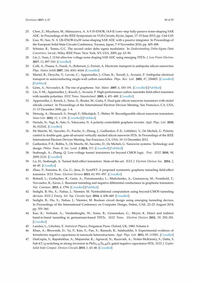
Electronics 2017, 6, 67 49 of 55
25. Chen, Z.; Miyahara, M.; Matsuzawa, A. A 9.35-ENOB, 14.8 fJ/conv-step fully-passive noise-shaping SARADC. In Proceedings of the IEEE Symposium on VLSI Circuits, Kyoto, Japan, 17–19 June 2015; pp. C64–C65.
26. Guo, W.; Sun, N. A 12b-ENOB 61µW noise-shaping SAR ADC with a passive integrator. In Proceedings ofthe European Solid-State Circuits Conference, Toyama, Japan, 7–9 November 2016; pp. 405–408.
27. Schreier, R.; Temes, G.C. The second order delta sigma modulator. In Understanding Delta-Sigma DataConverters, 1st ed.; Wiley-IEEE Press: New York, NY, USA, 2005; pp. 63–90.
28. Lin, J.; Yuan, J. 12-bit ultra-low voltage noise shaping SAR ADC using emerging TFETs. J. Low Power Electron.2017, 13, 497–510. [CrossRef]
29. Colli, A.; Pisana, S.; Fasoli, A.; Roberson, J.; Ferrari, A. Electronic transport in ambipolar silicon nanowires.Phys. Status Solidi 2007, 244, 4161–4164. [CrossRef]
30. Martel, R.; Deryche, V.; Lavoie, C.; Appenzeller, J.; Chan, K.; Tersoff, J.; Avouris, P. Ambipolar electricaltransport in semiconducting single-wall carbon nanotubes. Phys. Rev. Lett. 2001, 87, 256805. [CrossRef][PubMed]
31. Geim, A.; Novoselov, K. The rise of grapheme. Nat. Mater. 2007, 6, 183–191. [CrossRef] [PubMed]32. Lin, Y.-M.; Appenzeller, J.; Knoch, J.; Avouris, P. High-performance carbon nanotube field-effect transistor
with tunable polarities. IEEE Trans. Nanotechnol. 2005, 4, 451–489. [CrossRef]33. Appenzeller, J.; Knoch, J.; Tutuc, E.; Reuter, M.; Guha, S. Dual-gate silicon nanowire transistors with nickel
silicide contact. In Proceedings of the International Electron Devices Meeting, San Francisco, CA, USA,11–13 December 2006; pp. 1–4.
34. Heinzig, A.; Slesazeck, S.; Freupl, F.; Mikolajick, T.; Weber, W. Reconfigurable silicon nanowire transistors.Nano Lett. 2012, 12, 1–119. [CrossRef] [PubMed]
35. Harada, N.; Yagi, K.; Sato, S.; Yokoyama, N. A polarity-controllable graphene inverter. Appl. Phys. Lett. 2010,96, 012102. [CrossRef]
36. De Marchi, M.; Saccetto, D.; Frache, S.; Zhang, J.; Gaillardon, P.-E.; Leblebici, Y.; De Micheli, G. Polaritycontrol in double-gate, gate-all-around vertically stacked silicon nanowire FETs. In Proceedings of the IEEEInternational Electron Devices Meeting, San Francisco, CA, USA, 10–13 December 2012.
37. Gaillardon, P.-E.; Bobba, S.; De Marchi, M.; Saccetto, D.; De Micheli, G. Nanowire systems: Technology anddesign. Philos. Trans. R. Soc. Lond. A 2014, 372. [CrossRef] [PubMed]
38. Seabaugh, A.; Zhang, Q. Low-voltage tunnel transistors for beyond CMOS logic. Proc. IEEE 2010, 98,2095–2110. [CrossRef]
39. Lu, H.; Seabaugh, A. Tunnel field-effect transistors: State-of-the-art. IEEE J. Electron Devices Soc. 2014, 2,44–49. [CrossRef]
40. Zhao, P.; Feenstra, R.; Gu, G.; Jena, D. SymFET: A proposed symmetric graphene tunneling field-effecttransistor. IEEE Trans. Electron Devices 2013, 60, 951–957. [CrossRef]
41. Britnell, L.; Gorbachev, R.; Geim, A.; Ponomarenko, L.; Mishchenko, A.; Greenaway, M.; Fromhold, T.;Novoselov, K.; Eaves, L. Resonant tunneling and negative differential conductance in grapheme transistors.Nat. Commun. 2013, 4, 1794. [CrossRef] [PubMed]
42. Sedighi, B; Hu, X.; Nahas, J.; Niemier, M. Nontraditional computation using beyond-CMOS tunnelingdevices. IEEE J. Emerg. Sel. Top. Circuits Syst. 2014, 4, 438–449. [CrossRef]
43. Sedighi, B.; Hu, X.; Nahas, J.; Niemier, M. Boolean circuit design using emerging tunneling devices.In Proceedings of the International Conference on Computer Design, Dubai, UAE, 22–23 August 2014;pp. 355–360.
44. Kao, K.; Verhulst, A.; Vandenberghe, W.; Soree, B.; Groesneken, G.; Meyer, K. Direct and indirectband-to-band tunneling in germanium-based TFETs. IEEE Trans. Electron Devices 2012, 59, 292–301.[CrossRef]
45. Landau, L.; Lifschitz, E. Statistical Physics; Pergamon Press: Oxford, UK, 1980; Volume 6.46. Khan, A.; Bhowmik, D.; Yu, P.; Kim, S.; Pan, X.; Ramesh, R.; Salahuddin, S. Experimental evidence of
ferroelectric negative capacitance in nanoscale heterostructures. Appl. Phys. Lett. 2011, 99, 113501. [CrossRef]47. DasGupta, S.; Rajashekhar, A.; Majumdar, K.; Agrawal, N.; Razavieh, A.; Trolier-McKinstry, S.; Datta, S.
Sub-kT/q switching in strong inversion in PbZr0.52Ti0.48O3 gated negative capacitance FETs. IEEE J. Explor.Solid State Comput. Devices Circuits 2015, 1, 43–48. [CrossRef]
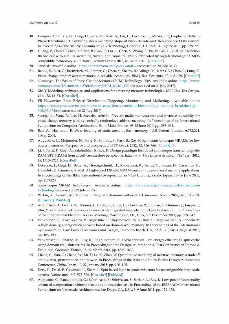
Electronics 2017, 6, 67 50 of 55
48. Frougier, J.; Shukla, N.; Deng, D.; Jerry, M.; Aziz, A.; Liu, L.; Lavallee, G.; Mayer, T.S.; Gupta, S.; Datta, S.Phase-transition-FET exhibiting steep switching slope of 8mV/decade and 36% enhanced ON current.In Proceedings of the 2016 Symposium on VLSI Technology, Honolulu, HI, USA, 14–16 June 2016; pp. 228–229.
49. Huang, P.; Chen, S.; Zhao, Y.; Chen, B.; Gao, B.; Liu, L.; Chen, Y.; Zhang, Z.; Bu, W.; We, H.; et al. Self-selectionRRAM cell with sub-uA switching current and robust reliability fabricated by high-k/metal gate CMOScompatible technology. IEEE Trans. Electron Devices 2016, 63, 4295–4301. [CrossRef]
50. Sandisk. Available online: https://www.rram-info.com/sandisk (accessed on 20 July 2017).51. Raoux, S.; Burr, G.; Breitwisch, M.; Rettner, C.; Chen, Y.; Shelby, R.; Salinga, M.; Krebs, D.; Chen, S.; Lung, H.
Phase-change random access memory: A scalable technology. IBM J. Res. Dev. 2010, 52, 465–479. [CrossRef]52. Numonyx. The Basics of Phase Change Memory (PCM) Technology. 2008. Available online: http://www.
numonyx.com/Documents/WhitePapers/PCM_Basics_WP.pdf (accessed on 20 July 2017).53. Xie, Y. Modeling, architecture, and applications for emerging memory technologies. IEEE Des. Test Comput.
2011, 28, 44–51. [CrossRef]54. PR Newswire: Press Release Distribution, Targeting, Monitoring and Marketing. Available online:
https://www.prnewswire.com/news.releases/ibm-scientists-achieve-storage-memory-breakthrough-300269117.html (accessed on 21 July 2017).
55. Seong, N.; Woo, F.; Lee, H. Security refresh: Prevent malicious wear-out and increase durability forphase-change memory with dynamically randomized address mapping. In Proceedings of the InternationalSymposium on Computer Architecture, Saint-Malo, France, 19–23 June 2010; pp. 383–394.
56. Ban, A.; Hasharon, R. Wear leveling of static areas in flash memory. U.S. Patent Number 6,732,221,4 May 2004.
57. Augustine, C.; Mojumder, N.; Fong, X.; Choday, S.; Park, S.; Roy, K. Spin-transfer torque MRAMs for lowpower memories: Perspective and prospective. IEEE Sens. J. 2012, 12, 756–766. [CrossRef]
58. Li, J.; Ndai, P.; Goel, A.; Salahuddin, S.; Roy, K. Design paradigm for robust spin-torque transfer magneticRAM (STT MRAM) from circuit/architecture perspective. IEEE Trans. Very Large Scale Integr. VLSI Syst. 2010,18, 1710–1723. [CrossRef]
59. Debrosse, J.; Gogl, D.; Bette, A.; Hoenigschmid, H.; Robertazzi, R.; Arndt, C.; Braun, D.; Casarotto, D.;Havreluk, R.; Lammers, S.; et al. A high-speed 128 Kbit MRAM core for future universal memory applications.In Proceedings of the IEEE International Symposium on VLSI Circuits, Kyoto, Japan, 12–14 June 2003;pp. 217–220.
60. Spin-Torque MRAM Technology. Available online: https://www.everspin.com/spin-torque-mram-technology (accessed on 22 July 2017).
61. Parkin, S.; Hayashi, M.; Thomas, L. Magnetic domain-wall racetrack memory. Science 2008, 320, 190–194.[CrossRef] [PubMed]
62. Annunziata, A.; Gaidis, M.; Thomas, L.; Chien, C.; Hung, C.; Chevalier, P.; Sullivan, E.; Hummel, J.; Joseph, E.;Zhu, Y.; et al. Racetrack memory cell array with integrated magnetic tunnel junction readout. In Proceedingsof the International Electron Devices Meetings, Washington, DC, USA, 5–7 December 2011; pp. 539–542.
63. Venkatesan, R.; Kozhikkottu, V.; Augustine, C.; Raychowdhury, A.; Roy, K.; Raghunathan, A. Tapechach:A high density, energy efficient cache based on domain wall memory. In Proceedings of the InternationalSymposium on Low Power Electronics and Design, Redondo Beach, CA, USA, 30 July–1 August 2012;pp. 185–190.
64. Venkatesan, R.; Sharad, M.; Roy, K.; Raghunathan, K. DWM-tapestri—An energy efficient all-spin cacheusing domain wall shift writes. In Proceedings of the Design, Automation & Test Conference in Europe &Exhibition, Grenoble, France, 18–22 March 2013; pp. 1825–1830.
65. Zhang, C.; Sun, G.; Zhang, W.; Mi, F.; Li, H.; Zhao, W. Quantitative modeling of racetrack memory, a tradeoffamong area, performance, and power. In Proceedings of the Asia and South Pacific Design AutomationConference, Chiba, Japan, 19–22 January 2015; pp. 100–105.
66. Dery, H.; Dalal, P.; Cywinski, L.; Sham, L. Spin-based logic in semiconductors for reconfigurable large-scalecircuits. Nature 2007, 447, 573–576. [CrossRef] [PubMed]
67. Augustine, C.; Panagopoulos, G.; Behin-Aein, B.; Srinivasan, S.; Sarkar, A.; Roy, K. Low-power functionalityenhanced computation architecture using spin-based devices. In Proceedings of the IEEE/ACM InternationalSymposium on Nanoscale Architectures, San Diego, CA, USA, 8–9 June 2011; pp. 129–136.
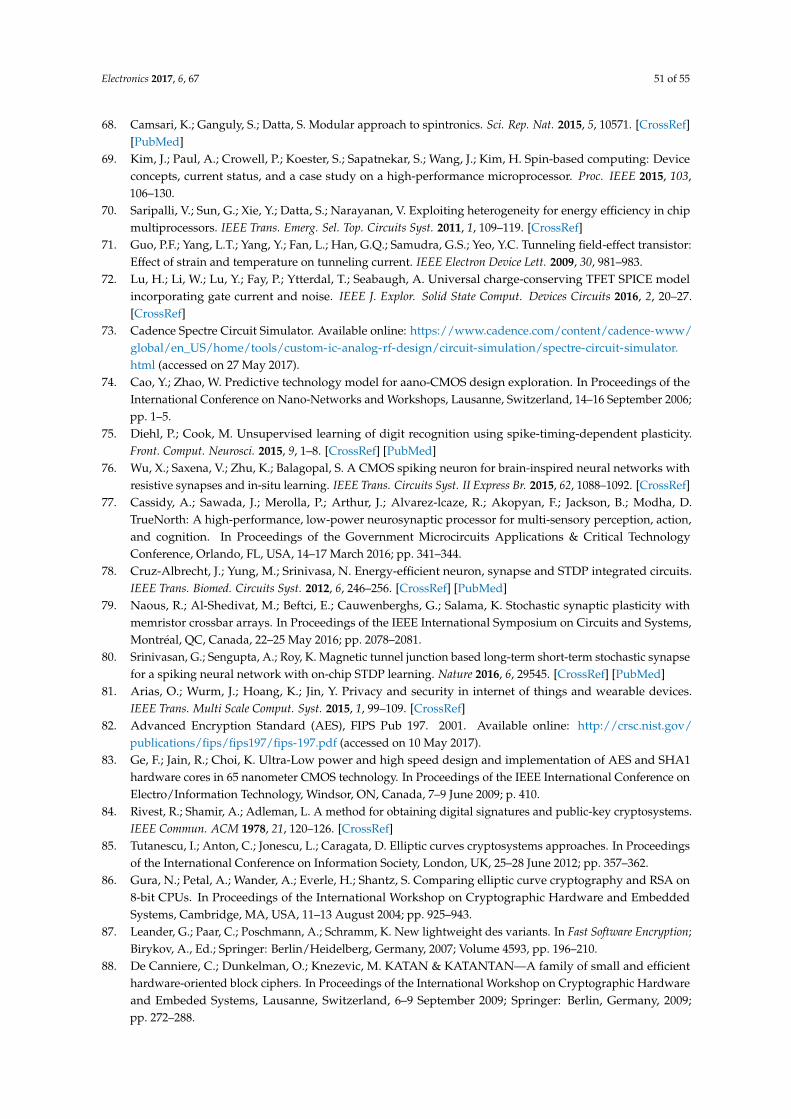
Electronics 2017, 6, 67 51 of 55
68. Camsari, K.; Ganguly, S.; Datta, S. Modular approach to spintronics. Sci. Rep. Nat. 2015, 5, 10571. [CrossRef][PubMed]
69. Kim, J.; Paul, A.; Crowell, P.; Koester, S.; Sapatnekar, S.; Wang, J.; Kim, H. Spin-based computing: Deviceconcepts, current status, and a case study on a high-performance microprocessor. Proc. IEEE 2015, 103,106–130.
70. Saripalli, V.; Sun, G.; Xie, Y.; Datta, S.; Narayanan, V. Exploiting heterogeneity for energy efficiency in chipmultiprocessors. IEEE Trans. Emerg. Sel. Top. Circuits Syst. 2011, 1, 109–119. [CrossRef]
71. Guo, P.F.; Yang, L.T.; Yang, Y.; Fan, L.; Han, G.Q.; Samudra, G.S.; Yeo, Y.C. Tunneling field-effect transistor:Effect of strain and temperature on tunneling current. IEEE Electron Device Lett. 2009, 30, 981–983.
72. Lu, H.; Li, W.; Lu, Y.; Fay, P.; Ytterdal, T.; Seabaugh, A. Universal charge-conserving TFET SPICE modelincorporating gate current and noise. IEEE J. Explor. Solid State Comput. Devices Circuits 2016, 2, 20–27.[CrossRef]
73. Cadence Spectre Circuit Simulator. Available online: https://www.cadence.com/content/cadence-www/global/en_US/home/tools/custom-ic-analog-rf-design/circuit-simulation/spectre-circuit-simulator.html (accessed on 27 May 2017).
74. Cao, Y.; Zhao, W. Predictive technology model for aano-CMOS design exploration. In Proceedings of theInternational Conference on Nano-Networks and Workshops, Lausanne, Switzerland, 14–16 September 2006;pp. 1–5.
75. Diehl, P.; Cook, M. Unsupervised learning of digit recognition using spike-timing-dependent plasticity.Front. Comput. Neurosci. 2015, 9, 1–8. [CrossRef] [PubMed]
76. Wu, X.; Saxena, V.; Zhu, K.; Balagopal, S. A CMOS spiking neuron for brain-inspired neural networks withresistive synapses and in-situ learning. IEEE Trans. Circuits Syst. II Express Br. 2015, 62, 1088–1092. [CrossRef]
77. Cassidy, A.; Sawada, J.; Merolla, P.; Arthur, J.; Alvarez-lcaze, R.; Akopyan, F.; Jackson, B.; Modha, D.TrueNorth: A high-performance, low-power neurosynaptic processor for multi-sensory perception, action,and cognition. In Proceedings of the Government Microcircuits Applications & Critical TechnologyConference, Orlando, FL, USA, 14–17 March 2016; pp. 341–344.
78. Cruz-Albrecht, J.; Yung, M.; Srinivasa, N. Energy-efficient neuron, synapse and STDP integrated circuits.IEEE Trans. Biomed. Circuits Syst. 2012, 6, 246–256. [CrossRef] [PubMed]
79. Naous, R.; Al-Shedivat, M.; Beftci, E.; Cauwenberghs, G.; Salama, K. Stochastic synaptic plasticity withmemristor crossbar arrays. In Proceedings of the IEEE International Symposium on Circuits and Systems,Montréal, QC, Canada, 22–25 May 2016; pp. 2078–2081.
80. Srinivasan, G.; Sengupta, A.; Roy, K. Magnetic tunnel junction based long-term short-term stochastic synapsefor a spiking neural network with on-chip STDP learning. Nature 2016, 6, 29545. [CrossRef] [PubMed]
81. Arias, O.; Wurm, J.; Hoang, K.; Jin, Y. Privacy and security in internet of things and wearable devices.IEEE Trans. Multi Scale Comput. Syst. 2015, 1, 99–109. [CrossRef]
82. Advanced Encryption Standard (AES), FIPS Pub 197. 2001. Available online: http://crsc.nist.gov/publications/fips/fips197/fips-197.pdf (accessed on 10 May 2017).
83. Ge, F.; Jain, R.; Choi, K. Ultra-Low power and high speed design and implementation of AES and SHA1hardware cores in 65 nanometer CMOS technology. In Proceedings of the IEEE International Conference onElectro/Information Technology, Windsor, ON, Canada, 7–9 June 2009; p. 410.
84. Rivest, R.; Shamir, A.; Adleman, L. A method for obtaining digital signatures and public-key cryptosystems.IEEE Commun. ACM 1978, 21, 120–126. [CrossRef]
85. Tutanescu, I.; Anton, C.; Jonescu, L.; Caragata, D. Elliptic curves cryptosystems approaches. In Proceedingsof the International Conference on Information Society, London, UK, 25–28 June 2012; pp. 357–362.
86. Gura, N.; Petal, A.; Wander, A.; Everle, H.; Shantz, S. Comparing elliptic curve cryptography and RSA on8-bit CPUs. In Proceedings of the International Workshop on Cryptographic Hardware and EmbeddedSystems, Cambridge, MA, USA, 11–13 August 2004; pp. 925–943.
87. Leander, G.; Paar, C.; Poschmann, A.; Schramm, K. New lightweight des variants. In Fast Software Encryption;Birykov, A., Ed.; Springer: Berlin/Heidelberg, Germany, 2007; Volume 4593, pp. 196–210.
88. De Canniere, C.; Dunkelman, O.; Knezevic, M. KATAN & KATANTAN—A family of small and efficienthardware-oriented block ciphers. In Proceedings of the International Workshop on Cryptographic Hardwareand Embeded Systems, Lausanne, Switzerland, 6–9 September 2009; Springer: Berlin, Germany, 2009;pp. 272–288.

Electronics 2017, 6, 67 52 of 55
89. Canniere, C.; Jaffe, J.; Jun, B. Differential power analysis. In Proceedings of the International CryptologyConference on Advances on Cryptology, Santa Barbara, CA, USA, 15–19 August 1999; Wiener, M., Ed.;Springer: Berlin, Germany, 1999; pp. 388–397.
90. Kocher, P. Design and validation strategy for obtaining assurance in countermeasures to power analysis andrelated. In Proceedings of the NIST Physical Security Workshop, Honolulu, HI, USA, 26–29 September 2005.
91. Akkar, M.; Giraud, C. An implementation of DES and AES, secure against some attacks. In Proceedingsof the Third International Workshop on Cryptographic Hardware and Embedded Systems, Paris, France,14–16 May 2001; Springer: Berlin, Germany, 2001; Volume 2162, pp. 309–318.
92. Yang, S.; Wolf, W.; Vijaykrishnan, N.; Serpanos, D.; Xie, Y. Power attack resistant cryptosystem design:A dynamic voltage and frequency switching approach. In Proceedings of the Design, Automation & TestConference in Europe & Exhibition, Washington, DC, USA, 7–11 March 2005; pp. 64–69.
93. Tiri, K.; Akmal, M.; Verbauwhede, I. A dynamic and differential CMOS logic with signal independent powerconsumption to withstand differential power analysis on smart cards. In Proceedings of the EuropeanSolid-State Circuits Conference, Firenze, Italy, 24–26 September 2002; pp. 403–406.
94. Bard, G.; Courtois, N.; Sepehrdad, J.; Zhang, B. Algebraic, aida/cube and side channel analysis of KATANfamily of block ciphers. In Proceedings of the International Conference on Cryptology in India, Hyderabad,India, 12–15 December 2010; pp. 176–196.
95. Ralston, P.; Suko, S.; Fry, D.; Calatayud, R.; Kober, R. Development approach for supply chain hardwareintegrity for electronics defense (SHIELD) using ultra-small “dielets” with encryption and senor capability,near field powering and communications. In Proceedings of the Government Microcircuit Applications &Critical Technology Conference, Orlando, FL, USA, 14–17 March 2016; pp. 97–100.
96. Rajendran, J.; Pino, Y.; Sinanoglu, O.; Karri, R. Logic encryption: A fault analysis perspective. In Proceedingsof the 2012 Design, Automation & Test in Europe Conference & Exhibition (DATE), Dresden, Germany,12–16 March 2012.
97. Chakraborty, R.; Bhunia, S. HARPOON: An obfuscation-based SoC design methodology for hardwareprotection. IEEE Trans. Comput. Aided Des. Integr. Circuits Syst. 2009, 28, 1493–1502. [CrossRef]
98. Yasin, M.; Rajendran, J.; Sinanoglu, O.; Karri, R. On improving the security of logic locking. IEEE Trans.Comput. Aided Des. Integr. Circuits Syst. 2016, 35, 1411–1424. [CrossRef]
99. Griffin, W.; Raghunathan, A.; Roy, K. CLIP: Circuit level IC protection through direct injection of processvariations. IEEE Trans. Very Large Scale Integr. Syst. 2012, 20, 791–803. [CrossRef]
100. Alasad, Q.; Bi, Y.; Yuan, J. E2LEMI: Energy-efficient logic encryption using multiplexer insertion. Electronics2017, 6, 16. [CrossRef]
101. Subramanyan, P.; Ray, S.; Malik, S. Evaluating the security of logic encryption algorithms. In Proceedingsof the IEEE International Symposium on Hardware Oriented Security and Trust, Washington, DC, USA,5–7 May 2015; pp. 137–143.
102. Xie, Y.; Srivastava, A. Mitigating SAT Attack on Logic Locking. Lecture Notes in Computer Science,Proceeding of the Cryptographic Hardware and Embedded Systems—CHES 2016, Santa Barbara, CA, USA,17–19 August 2016; Springer: Berlin, Gemany, 2016; Volume 9813, pp. 127–146.
103. Yasin, M.; Mazumdar, B.; Rajendran, J.; Sinanoglu, O. SARLock: SAT attack resistant logic Locking.In Proceedings of the IEEE International Symposium on Hardware Oriented Security and Trust, McLean,VA, USA, 3–5 May 2016; pp. 236–241.
104. Yasin, M.; Mazumdar, B.; Sinanoglu, O.; Rajendran, J. Security analysis of anti-SAT. In Proceedings of theAsia and South Pacific Design Automation Conference, Chiba, Japan, 16–19 January 2017; pp. 342–347.
105. Alasa, Q.; Yuan, J.; Fan, D. Leveraging all-spin logic to improve hardware security. In Proceedings of theACM Great Lake Symposium on VLSI, Banff, AB, Canada, 10–12 May 2017; pp. 491–494.
106. Imeson, F.; Emtenan, A.; Garg, S.; Tripunitara, M. Securing computer hardware using 3D integrated circuit(IC) technology and split manufacturing for obfuscation. In Proceedings of the USENIX Security Symposium,Washington, DC, USA, 14–16 August 2013; pp. 495–510.
107. Rajendran, J.; Sinanoglu, O.; Karri, R. Is split manufacturing secure? In Proceedings of the Design,Automation & Test in Europe Conference & Exhibition, Grenoble, France, 18–22 March 2013; pp. 1259–1264.
108. Vaidyanathan, K.; Das, B.; Sumbul, E.; Liu, R.; Pileggi, L. Building trusted ICs using split fabrication.In Proceedings of the IEEE International Symposium on Hardware-Oriented Security and Trust, Arlington,VA, USA, 6–7 May 2014.
Electronics 2017, 6, 67 53 of 55
109. Vaidyanathan, K.; Liu, R.; Sumbul, E.; Zhu, Q.; Franchetti, F.; Pileggi, L. Efficient and secure intellectualproperty (IP) design with split fabrication. In Proceedings of the IEEE International Symposium onHardware-Oriented Security and Trust, Arlington, VA, USA, 6–7 May 2014.
110. Jagasivamani, M.; Gadfort, P.; Sika, M.; Bajura, M.; Fritze, M. Split-fabrication obfuscation: Metrics andtechniques. In Proceedings of the IEEE International Symposium on Hardware-Oriented Security and Trust,Arlington, VA, USA, 6–7 May 2014.
111. Hill, B.; Karmazin, R.; Otero, C.T.O.; Tse, J.; Manohar, R. A split-foundry asynchronous FPGA. In Proceedingsof the Custom Integrated Circuits Conference, San Jose, CA, USA, 22–25 September 2013; pp. 1–4.
112. Xie, Y.; Bao, C.; Serafy, C.; Lu, T.; Srivastava, A.; Tehranipoor, M. Security and vulnerability implications of3D ICs. IEEE Trans. Multi Scale Comput. Syst. 2016, 2, 108–122. [CrossRef]
113. Hunt, J.; Ding, Y.; Hsieh, A.; Chen, J.; Huang, D. Synergy between 2.5/3D development and hybrid 3Dwafer level fanout. In Proceedings of the Electronic System-Integration Technology Conference, Amsterdam,The Netherlands, 17–20 September 2012; pp. 1–10.
114. Narasimhan, S.; Du, D.; Subhra, R.; Chakraborty, S.; Paul, S.; Wolff, F.; Papachristou, C.; Roy, K.; Bhunia, S.Hardware Trojan detection by multiple-parameter side-channel analysis. IEEE Trans. Comput. 2013, 62,2183–2194. [CrossRef]
115. Van Woudenberg, J.; Witteman, M.; Bakker, B. Improving differential power analysis by elastic alignment.In Proceedings of the International Conference on Topics in Cryptology—CT-RSA 2011, San Francisco, CA,USA, 14–18 February 2011; Springer: Berlin, Germany; pp. 104–119.
116. Frontier Economics. Estimating the Global Economic and Social Impacts of Counterfeiting and Piracy;Technical Report; Frontier Economics Ltd.: London, UK, 2011.
117. Ronald, P.; James, P.; Bryan, J. Building Block for a Secure CMOS Logic Cell Library. U.S. Patent 20100301903 A1,2 December 2010. Available online: http://www.google.com/patents/US20100301903 (accessed on 10 June 2017).
118. Chow, L.; Baukus, J.; Wang, J.; Cocchi, R. Camouflaging a Standard Cell Based Integrated Circuit. U.S. Patent8151235 B2, 3 April 2012. Available online: http://www.google.com/patents/US8151235 (accessed on1 July 2017).
119. Rajendran, J.; Sinanoglu, O.; Sam, M.; Karri, R. Security analysis of integrated circuit camouflaging.In Proceedings of the ACM Conference on Computer and Communications Security, Berlin, Germany,4–8 November 2013; pp. 709–720.
120. Stoica, A.; Zebulum, R.; Keymeulen, D.; Ferguson, M.; Duong, V. Taking evolutionary circuit design fromexperimentation to implementation: Some useful techniques and a silicon demonstration. IEE Proc. Comput.Digit. Tech. 2004, 151, 295–300. [CrossRef]
121. Ruzicka, R. New polymorphic NAND/XOR gate. In Proceedings of the International Conference on AppliedComputer Science, Las Vegas, NV, USA, 25–28 June 2007; pp. 192–196.
122. Bi, Y.; Shamsi, K.; Yuan, J.-S.; Gaillardon, P.; De Micheli, G.; Yin, X.; Hu, X.; Niemier, M. Emergingtechnology-based design of primitives for hardware security. ACM J. Emerg. Technol. Comput. Syst. 2016, 13,1–19. [CrossRef]
123. Alasad, B.; Jiann-Shiun Yuan, J.S.; Bi, Y. Logic Obfuscation against IC Reverse Engineering Attacks usingPolymorphic Gates. In Proceedings of the IEEE International Conference on Computer Design, Boston, MA,USA, 5–8 November 2017; pp. 1–4.
124. Vatajelu, E.; Natale, G.; Torres, L.; Prinetto, P. STT-MRAM-based strong PUF architecture. In Proceedings ofthe IEEE Computer Society Annual Symposium on VLSI, Montpellier, France, 8–10 July 2015; pp. 467–472.
125. Zhang, L.; Fonf, X.; Chang, C.-H.; Kong, Z.; Roy, K. Highly reliable memory-based physical unclonablefunction using spin-transfer torque MRAM. In Proceedings of the IEEE International Symposium on Circuitsand Systems, Melbourne, VIC, Australia, 1–5 June 2014; pp. 2069–2172.
126. Oosawa, S.; Konishi, T.; Onizawa, N.; Hanyu, T. Design of an STT-MTJ based true random number generatorusing digitally controlled probability-locked loop. In Proceedings of the IEEE International New Circuitsand Systems Conference, Grenoble, France, 7–10 June 2015; pp. 1–4.
127. Kannan, S.; Karimi, N.; Sinanoglu, O.; Karri, R. Security vulnerabilities of emerging nonvolatile mainmemories and countermeasures. IEEE Trans. Comput. Aided Des. Integr. Circuits Syst. 2014, 34, 2–15.[CrossRef]
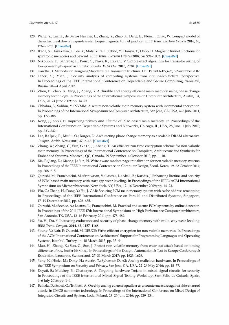
Electronics 2017, 6, 67 54 of 55
128. Wang, Y.; Cai, H.; de Barros Naviner, L.; Zhang, Y.; Zhao, X.; Deng, E.; Klein, J.; Zhao, W. Compact model ofdielectric breakdown in spin-transfer torque magnetic tunnel junction. IEEE Trans. Electron Devices 2016, 63,1762–1767. [CrossRef]
129. Ikeda, S.; Hayakawa, J.; Lee, Y.; Matsukura, F.; Ohno, Y.; Hanyu, T.; Ohno, H. Magnetic tunnel junctions forspintronic memories and beyond. IEEE Trans. Electron Devices 2007, 54, 991–1002. [CrossRef]
130. Nikoubin, T.; Bahrebar, P.; Pouri, S.; Navi, K.; Iravani, V. Simple exact algorithm for transistor sizing oflow-power high-speed arithmetic circuits. VLSI Des. 2010, 2010. [CrossRef]
131. Gandhi, D. Methods for Designing Standard Cell Transistor Structures. U.S. Patent 6,477,695, 5 November 2002.132. Taheri, S.; Yuan, J. Security analysis of computing systems from circuit-architectural perspective.
In Proceedings of the IEEE International Conference on Dependable and Secure Computing, Yaroslavl,Russia, 20–24 April 2017.
133. Zhou, P.; Zhao, B.; Yang, J.; Zhang, Y. A durable and energy efficient main memory using phase changememory technology. In Proceedings of the International Symposium on Computer Architecture, Austin, TX,USA, 20–24 June 2009; pp. 14–23.
134. Chhabra, S.; Solihin, Y. iNVMM: A secure non-volatile main memory system with incremental encryption.In Proceedings of the International Symposium on Computer Architecture, San Jose, CA, USA, 4–8 June 2011;pp. 177–188.
135. Kong, J.; Zhou, H. Improving privacy and lifetime of PCM-based main memory. In Proceedings of theInternational Conference on Dependable Systems and Networks, Chicago, IL, USA, 28 June–1 July 2010;pp. 333–342.
136. Lee, B.; Ipek, E.; Mutlu, O.; Burger, D. Architecting phase change memory as a scalable DRAM alternative.Comput. Archit. News 2009, 37, 2–13. [CrossRef]
137. Zhang, X.; Zhang, C.; Sun, G.; Di, J.; Zhang, T. An efficient run-time encryption scheme for non-valatilemain memory. In Proceedings of the International Conference on Compilers, Architecture and Synthesis forEmbedded Systems, Montreal, QC, Canada, 29 September–4 October 2013; pp. 1–10.
138. Xia, F.; Jiang, D.; Xiaong, J.; Sun, N. Write-aware random page initialization for non-volatile memory systems.In Proceedings of the IEEE International Conference on Computer Design, Seoul, Korea, 19–22 October 2014;pp. 208–215.
139. Qureshi, M.; Franchescini, M.; Srinivasan, V.; Lastras, L.; Abali, B.; Karidis, J. Enhancing lifetime and securityof PCM-based main memory with start-gap wear leveling. In Proceedings of the IEEE/ACM InternationalSymposium on Microarchitecture, New York, NY, USA, 12–16 December 2009; pp. 14–23.
140. Wu, G.; Zhang, H.; Dong, Y.; Hu, J. CAR: Securing PCM main memory system with cache address remapping.In Proceedings of the IEEE International Conference on Parallel and Distributed Systems, Singapore,17–19 December 2012; pp. 626–635.
141. Qureshi, M.; Seznec, A.; Lastras, L.; Franceschini, M. Practical and secure PCM systems by online detection.In Proceedings of the 2011 IEEE 17th International Symposium on High Performance Computer Architecture,San Antonio, TX, USA, 12–16 February 2011; pp. 478–489.
142. Yu, H.; Du, Y. Increasing endurance and security of phase-change memory with multi-way wear-leveling.IEEE Trans. Comput. 2014, 63, 1157–1168.
143. Young, V.; Nair, P.; Quershi, M. DEUCE: Write-efficient encryption for non-volatile memories. In Proceedingsof the ACM International Conference on Architectural Support for Programming Languages and OperatingSystems, Istanbul, Turkey, 14–18 March 2015; pp. 33–44.
144. Mao, H.; Zhang, X.; Sun, G.; Sun, J. Protect non-volatile memory from wear-out attack based on timingdifference of row buffer hit/miss. In Proceedings of the Design, Automation & Test in Europe Conference &Exhibition, Lausanne, Switzerland, 27–31 March 2017; pp. 1623–1626.
145. Yang, K.; Hicks, M.; Dong, H.; Austin, T.; Sylvester, D. A2: Analog malicious hardware. In Proceedings ofthe IEEE Symposium on Security and Privacy, San Jose, CA, USA, 22–26 May 2016; pp. 18–37.
146. Deyati, S.; Muldrey, B.; Chatterjee, A. Targeting hardware Trojans in mixed-signal circuits for security.In Proceedings of the IEEE International Mixed-Signal Testing Workshop, Sant Feliu de Guixols, Spain,4–6 July 2016; pp. 1–4.
147. Bellizia, D.; Scotti, G.; Trifiletti, A. On-chip analog current equalizer as a countermeasure against side-channelattacks in CMOS nanometer technology. In Proceedings of the International Conference on Mixed Design ofIntegrated Circuits and System, Lodz, Poland, 23–25 June 2016; pp. 229–234.
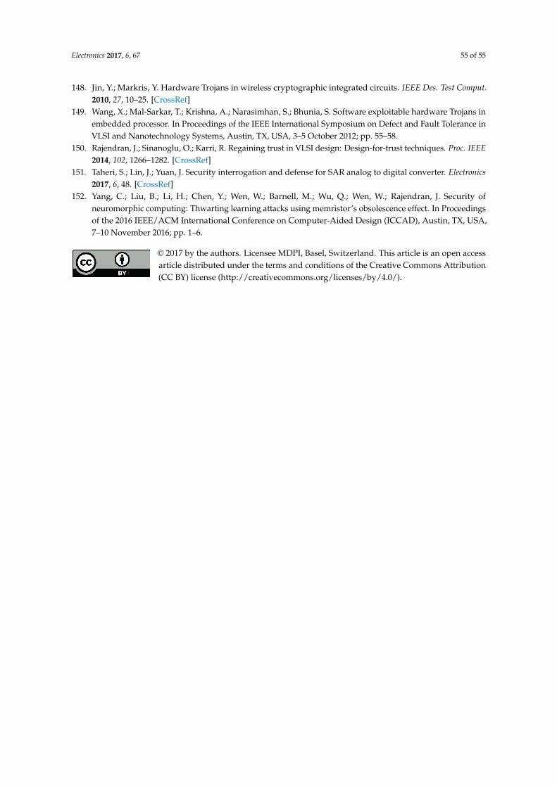
Electronics 2017, 6, 67 55 of 55
148. Jin, Y.; Markris, Y. Hardware Trojans in wireless cryptographic integrated circuits. IEEE Des. Test Comput.2010, 27, 10–25. [CrossRef]
149. Wang, X.; Mal-Sarkar, T.; Krishna, A.; Narasimhan, S.; Bhunia, S. Software exploitable hardware Trojans inembedded processor. In Proceedings of the IEEE International Symposium on Defect and Fault Tolerance inVLSI and Nanotechnology Systems, Austin, TX, USA, 3–5 October 2012; pp. 55–58.
150. Rajendran, J.; Sinanoglu, O.; Karri, R. Regaining trust in VLSI design: Design-for-trust techniques. Proc. IEEE2014, 102, 1266–1282. [CrossRef]
151. Taheri, S.; Lin, J.; Yuan, J. Security interrogation and defense for SAR analog to digital converter. Electronics2017, 6, 48. [CrossRef]
152. Yang, C.; Liu, B.; Li, H.; Chen, Y.; Wen, W.; Barnell, M.; Wu, Q.; Wen, W.; Rajendran, J. Security ofneuromorphic computing: Thwarting learning attacks using memristor’s obsolescence effect. In Proceedingsof the 2016 IEEE/ACM International Conference on Computer-Aided Design (ICCAD), Austin, TX, USA,7–10 November 2016; pp. 1–6.
© 2017 by the authors. Licensee MDPI, Basel, Switzerland. This article is an open accessarticle distributed under the terms and conditions of the Creative Commons Attribution(CC BY) license (http://creativecommons.org/licenses/by/4.0/).
Related Documents