Ultra-fast all-optical signal processing: towards optical packet switching Y. Liu a , E. Tangdiongga a , Z. Li a , S. Zhang a , M.T. Hill a , J.H.C. van Zantvoort a , F.M. Huijskens a , H. de Waardt a , M.K. Smit b , A.M.J. Koonen a , G.D. Khoe a and H.J.S. Dorren a a Electro-Optical Communication group, COBRA Research Institute, Eindhoven University of Technology, P. O. Box 513, 5600 MB, Eindhoven, the Netherlands. Email: [email protected] b Opto-Electronic Devices group, COBRA Research Institute, Eindhoven University of Technology, P. O. Box 513, 5600 MB, Eindhoven, the Netherlands. ABSTRACT We present some progress in the field of optical signal processing that could be utilized in all-optical packet switching. We demonstrate error-free 160 Gb/s optical wavelength conversion employing a single semiconductor optical amplifier. The gain recovery time of the semiconductor optical amplifier is greater than 90 ps. Assisted by an optical bandpass filter, an effective recovery time of 3 ps is achieved in the wavelength converter, which ensures 160 Gb/s operation. This optical wavelength converter can be controlled by a monolithically integrated optical flip-flop memory to route 80 Gb/s data-packets all-optically. The routing is realized without electronic control. The integrated optical flip-flop is based on two-coupled lasers, exhibits single-mode operation, has 35 dB contrast ratio between the states and switches state in about 2 ns. We demonstrate that the integrated flip-flop is able to control the optical wavelength converter up to 160 Gb/s. The system is capable of routing 80 Gb/s data packets with duration of 35 ns, separated by 15 ns of guard time. Keywords: Optical fiber communication, optical cross-connect, optical packet switching, optical signal processing, semiconductor optical amplifier, optical storage, optical memory, optical wavelength conversion, wavelength routing. 1. INTRODUCTION Optical packet switches attract research interest as they might solve the current bandwidth mismatch between optical transmission and electronic routers, by switching, routing and forwarding optical data packets in the physical layer to maintain high data rates, transparency and efficiency of the optical network. Optical packet switching offers advantages in terms of power consumption, foot-print and switching architectures compared to their electronic counterparts [1-9]. A number of optical packet switching has been investigated [1-8]. Utilizing all-optical signal processing to realize optical packet switching is promising [2-7], because packet switching could be carried out entirely in the optical domain. This means that the bottleneck of optical-to-electrical-to-optical conversion can be eliminated. An 1x2 all-optical packet switching is demonstrated in [3] utilizing entirely all-optical signal processing. The all-optical packet switch comprises an all-optical header processor, an all-optical flip-flop memory, and an optical wavelength converter. The header processor translates the optical header pattern into an optical pulse. This pulse triggers the optical flip-flop to generate continuous wave (CW) light with a specific wavelength. Hence, different header information forces the optical flip-flop to output CW light with a different wavelength. The output light from the optical flip-flop is fed into the wavelength converter to convert the packet into the desired wavelength. Afterwards, a demultiplexer is used to route the packet into a specific port, depending on the wavelength of the packet. Thus the routing of the packet is determined by the wavelength of the optical flip-flop output light, in turn, determined by the header information. Thus an optical Invited Paper Optical Transmission, Switching, and Subsystems IV, edited by Chang Soo Park, Shizhong Xie, Curtis R. Menyuk, Ken-ichi Kitayama, Proc. of SPIE Vol. 6353, 635312, (2006) · 0277-786X/06/$15 · doi: 10.1117/12.687147 Proc. of SPIE Vol. 6353 635312-1

Welcome message from author
This document is posted to help you gain knowledge. Please leave a comment to let me know what you think about it! Share it to your friends and learn new things together.
Transcript
Ultra-fast all-optical signal processing: towards optical packet switching
Y. Liua, E. Tangdionggaa, Z. Lia, S. Zhanga, M.T. Hilla, J.H.C. van Zantvoorta, F.M. Huijskensa, H. de Waardta, M.K. Smitb, A.M.J. Koonena, G.D. Khoea and H.J.S. Dorrena
aElectro-Optical Communication group, COBRA Research Institute, Eindhoven University of Technology, P. O. Box 513, 5600 MB, Eindhoven, the Netherlands. Email: [email protected]
bOpto-Electronic Devices group, COBRA Research Institute, Eindhoven University of Technology, P. O. Box 513, 5600 MB, Eindhoven, the Netherlands.
ABSTRACT
We present some progress in the field of optical signal processing that could be utilized in all-optical packet switching. We demonstrate error-free 160 Gb/s optical wavelength conversion employing a single semiconductor optical amplifier. The gain recovery time of the semiconductor optical amplifier is greater than 90 ps. Assisted by an optical bandpass filter, an effective recovery time of 3 ps is achieved in the wavelength converter, which ensures 160 Gb/s operation. This optical wavelength converter can be controlled by a monolithically integrated optical flip-flop memory to route 80 Gb/s data-packets all-optically. The routing is realized without electronic control. The integrated optical flip-flop is based on two-coupled lasers, exhibits single-mode operation, has 35 dB contrast ratio between the states and switches state in about 2 ns. We demonstrate that the integrated flip-flop is able to control the optical wavelength converter up to 160 Gb/s. The system is capable of routing 80 Gb/s data packets with duration of 35 ns, separated by 15 ns of guard time.
Keywords: Optical fiber communication, optical cross-connect, optical packet switching, optical signal processing, semiconductor optical amplifier, optical storage, optical memory, optical wavelength conversion, wavelength routing.
1. INTRODUCTION Optical packet switches attract research interest as they might solve the current bandwidth mismatch between optical transmission and electronic routers, by switching, routing and forwarding optical data packets in the physical layer to maintain high data rates, transparency and efficiency of the optical network. Optical packet switching offers advantages in terms of power consumption, foot-print and switching architectures compared to their electronic counterparts [1-9]. A number of optical packet switching has been investigated [1-8]. Utilizing all-optical signal processing to realize optical packet switching is promising [2-7], because packet switching could be carried out entirely in the optical domain. This means that the bottleneck of optical-to-electrical-to-optical conversion can be eliminated. An 1x2 all-optical packet switching is demonstrated in [3] utilizing entirely all-optical signal processing. The all-optical packet switch comprises an all-optical header processor, an all-optical flip-flop memory, and an optical wavelength converter. The header processor translates the optical header pattern into an optical pulse. This pulse triggers the optical flip-flop to generate continuous wave (CW) light with a specific wavelength. Hence, different header information forces the optical flip-flop to output CW light with a different wavelength. The output light from the optical flip-flop is fed into the wavelength converter to convert the packet into the desired wavelength. Afterwards, a demultiplexer is used to route the packet into a specific port, depending on the wavelength of the packet. Thus the routing of the packet is determined by the wavelength of the optical flip-flop output light, in turn, determined by the header information. Thus an optical
Invited Paper
Optical Transmission, Switching, and Subsystems IV, edited byChang Soo Park, Shizhong Xie, Curtis R. Menyuk, Ken-ichi Kitayama,
Proc. of SPIE Vol. 6353, 635312, (2006) · 0277-786X/06/$15 · doi: 10.1117/12.687147
Proc. of SPIE Vol. 6353 635312-1
packet switch is realized. It can be seen that all-optical wavelength converters and all-optical flip-flop memories are essential building blocks in all-optical packet switches. Optical wavelength converters that utilize nonlinearities of semiconductor optical amplifiers (SOAs) have attracted considerable research interest due to the integration ability and power efficiency [9]. A number of SOA-based wavelength converters have been demonstrated [10-13, 16-18, 22-24]. Monolithically integrated devices that contain a 40 Gb/s optical wavelength converter with a sub-nanosecond tunable laser has been realized [10].However, the slow SOA recovery time can cause unwanted pattern effects in the converted signal, which limits the maximum operation speed. Some methods have been proposed to increase the frequency response of an SOA-based wavelength converter. An increased operation speed has been achieved by employing a Fiber Bragg Grating (FBG) [14], or a waveguide filter [15]. The speed response of SOAs can also be enhanced by using two cascaded SOAs configuration so called ‘Turbo-Switch’ as presented in [16]. Wavelength conversion at 100 Gb/s has been achieved by using a long SOA (2 mm) in combination with a Fiber Bragg Grating (FBG) [13]. It has been demonstrated in [17] that a wavelength converter based on a delayed-interferometric configuration can achieve 168 Gb/s and this approach also allows photonic integration [18]. A theoretical analysis for this concept of the delayed-interferometric configuration has been given in [19]. The delayed-interferometer also acts as an optical filter. Ref. [20, 21] shows theoretically how optical filtering can increase the modulation bandwidth of SOA-based switches. Optical filtering of chirped converted output light of an SOA can be utilized to achieve polarity-preserved wavelength conversion at 40 Gb/s [22-24]. It has been shown in [22] that the red-chirped component of the converted output light, filtered by an optical step-filter (with a sharp frequency response) can be used to obtain non-inverted wavelength conversion. Similarly, Ref. [23] shows that filtering the blue-chirped part of the converted output light could lead to non-inverted wavelength conversion. In [24], both the blue- and red-chirped components of the converted signals are filtered by a pulse reformatting optical filter to achieve non-inverted wavelength conversion. In this paper, we present error-free SOA-based 160 Gb/s wavelength conversion assisted by an optical filter. Another essential building block of an all-optical packet switch is optical flip-flop memories, which are used to store the switch decision information. It has been demonstrated in [3] that an optical flip-flop based on two symmetrically coupled lasers can control an optical packet switch. In that particular configuration, the optical flip-flop state was set by an optical header recognizer, and the flip-flop controls a wavelength routing switch. The flip-flop presented in [3] had a switching time of about 2 µs, since it was implemented using fiber pig-tailed components. It has been presented in [6] that an integrated optical flip-flop can control a wavelength converter to switch a 10 Gb/s data packet. In this paper we will present a different integrated optical flip-flop and its performance for 80 Gb/s all-optical packet switching. In this paper, we firstly present an error-free and pattern-independent 160 Gb/s wavelength conversion with low power penalty using a single SOA [11]. The SOA in the experiment has an initial gain recovery time greater than 90 ps. We demonstrate that the effective recovery time of the SOA can be dramatically shortened to less than 3 ps with the assistance of an optical bandpass filter. A delayed-interferometer is utilized to change the inverted signal into non-inverted signal. We obtained our results using commercially available fiber pigtailed components. The system is easy to implement since the configuration is simple. Moreover, this concept allows photonic integration. Furthermore, we demonstrate that a monolithically integrated optical flip-flop is capable of controlling an SOA-based all-optical wavelength converter to route 80 Gb/s data packets all-optically. The routing is realized without using electronic control. The data packets have duration time of 35 ns, and are separated by a guard time of 15 ns. The optical flip-flop exhibits single-mode operation, has a 35 dB contrast ratio between the states, and switches state in about 2 ns. A clear open eye indicates that the system can also operate error-free at 160 Gb/s.
2. 160 GB/S ALL-OPTICAL WAVELENGTH CONVERTER In this section, firstly we will explain how a detuned optical bandpass filter can be applied to speed up the recovery of the SOA-based system where a slow gain recovery SOA is used. The operation principle of ultra-fast recovery is explained. Afterwards experimental results are presented. Finally this section is ended with conclusions.
Proc. of SPIE Vol. 6353 635312-2

2.1 Operation principle of ultra-fast recovery
A setup for measuring the recovery time of the SOA is depicted in Figure 1a. A pulsed pump signal is combined with a continuous wave (CW) probe signal, and the signals are simultaneously launched into the SOA. At the output of the SOA, an OBF is used to select the probe light, and to block the pump signal. The OBF in this measurement has a 3-dB bandwidth of 10 nm. The probe light that outputs the OBF is monitored by an optical sampling scope (Agilent 86119A) with an optical bandwidth up to 700 GHz. The pulse width of pump signal is 2.2 ps, as shown in Figure 1b. Figure 1: (a) The setup for testing the SOA gain recovery. (b) The input pump pulse. (c) The SOA gain recovery measured by an optical sampling scope. BPF is (optical) bandpass filter. We firstly use the optical sampling scope to measure the SOA recovery if the central wavelength of the OBF is located at the center wavelength. The result is shown in Figure 1c. Figure 1 summarizes some well-known results. The saturating optical pump light depletes the SOA gain. The gain saturation is a fast process dominated by stimulated emission, and follows in good approximation the pulse-shape. The SOA gain approximately reaches its minimum at the time that the input pump pulse reaches its maximum power. We also notice that the SOA gain recovery has a fast and a slow component. Roughly speaking the SOA recovers on three different time-scales. Ultrafast gain recovery, driven by carrier-carrier scattering takes place at sub-picosecond timescales [25]. Furthermore, carrier-phonon interactions contribute to the recovery of the amplifier on a timescale of a few picoseconds. Finally, on a nanosecond time scale in the SOA recovery, there is a contribution driven by electron-hole interactions. The injected pulses not only modulate the gain of the SOA, but also modulate the refractive index of the SOA. This results in chirp on the output signal. The leading edges of the (inverted) converted probe pulses are red-shifted, whereas the trailing edges are blue-shifted [22-24]. We use our model [26, 27] to compute the chirp of the converted pulse. The simulation result is presented in the lower panel of Figure 2. A similar result can be found in [24]. For reasons of comparison, the gain recovery is shown in the upper panel of Figure 2, which is in a good agreement with the experimental curve (Figure 1c).
Figure 2: The simulated SOA gain (upper panel) and chirp response (lower panel) as a function of time.
Time base: 2 ps/div
(b) Input pump pulse
Zero
Pow
er (
A.U
.)
(c) Gain response of SOA
3dB SOA
BPF
CW Probe
Pump Pulses
Probe
(a) Setup
Time base: 2 ps/div Zero
Pow
er (
A.U
.)
0 2 4 6 8 10 12 14 16 18 20
-100
-50
0
50 0.4
0.6
0.8
1
Inte
nsity
(
a. u
.)
Time (ps)
Chi
rp
(GH
z)
red-shift
blue-shift
Proc. of SPIE Vol. 6353 635312-3
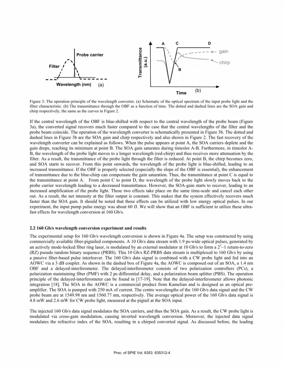
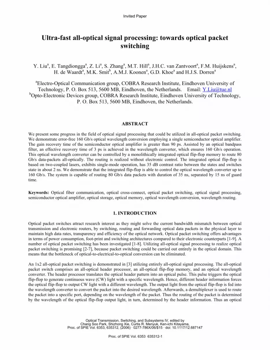
Figure 3: The operation principle of the wavelength converter. (a) Schematic of the optical spectrum of the input probe light and the filter characteristic. (b) The transmittance through the OBF as a function of time. The dotted and dashed lines are the SOA gain and chirp respectively, the same as the curves in Figure 2. If the central wavelength of the OBF is blue-shifted with respect to the central wavelength of the probe beam (Figure 3a), the converted signal recovers much faster compared to the case that the central wavelengths of the filter and the probe beam coincide. The operation of the wavelength converter is schematically presented in Figure 3b. The dotted and dashed lines in Figure 3b are the SOA gain and chirp respectively and also shown in Figure 2. The fast recovery of the wavelength converter can be explained as follows. When the pulse appears at point A, the SOA carriers deplete and the gain drops, reaching its minimum at point B. The SOA gain saturates during timeslot A-B. Furthermore, in timeslot A-B, the wavelength of the probe light moves to a longer wavelength (red-chirp) and thus receives more attenuation by the filter. As a result, the transmittance of the probe light through the filter is reduced. At point B, the chirp becomes zero, and SOA starts to recover. From this point onwards, the wavelength of the probe light is blue-shifted, leading to an increased transmittance. If the OBF is properly selected (especially the slope of the OBF is essential), the enhancement of transmittance due to the blue-chirp can compensate the gain saturation. Thus, the transmittance at point C is equal to the transmittance at point A. From point C to point D, the wavelength of the probe light slowly moves back to the probe carrier wavelength leading to a decreased transmittance. However, the SOA-gain starts to recover, leading to an increased amplification of the probe light. These two effects take place on the same time-scale and cancel each other out. As a result, the net intensity at the filter output is constant. This makes that the system effectively recovers much faster than the SOA gain. It should be noted that these effects can be utilized with low energy optical pulses. In our experiment, the input pump pulse energy was about 60 fJ. We will show that an OBF is sufficient to utilize these ultra-fast effects for wavelength conversion at 160 Gb/s. 2.2 160 Gb/s wavelength conversion experiment and results
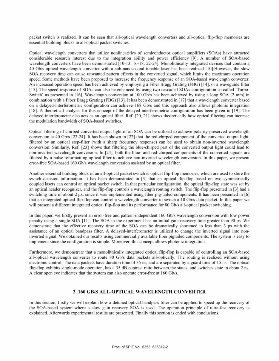
The experimental setup for 160 Gb/s wavelength conversion is shown in Figure 4a. The setup was constructed by using commercially available fiber-pigtailed components. A 10 Gb/s data stream with 1.9 ps-wide optical pulses, generated by an actively mode-locked fiber ring laser, is modulated by an external modulator at 10 Gb/s to form a 27−1 return-to-zero (RZ) pseudo random binary sequence (PRBS). This 10 Gb/s RZ-PRBS data stream is multiplexed to 160 Gb/s by using a passive fiber-based pulse interleaver. The 160 Gb/s data signal is combined with a CW probe light and fed into an AOWC via a 3 dB coupler. As shown in the dashed box of Figure 4a, the AOWC is composed out of an SOA, a 1.4 nm OBF and a delayed-interferometer. The delayed-interferometer consists of two polarization controllers (PCs), a polarization maintaining fiber (PMF) with 2 ps differential delay, and a polarization beam splitter (PBS). The operation principle of the delayed-interferometer can be found in [17-19]. Note that the delayed-interferometer allows photonic integration [18]. The SOA in the AOWC is a commercial product from Kamelian and is designed as an optical pre-amplifier. The SOA is pumped with 250 mA of current. The centre wavelengths of the 160 Gb/s data signal and the CW probe beam are at 1549.98 nm and 1560.77 nm, respectively. The average optical power of the 160 Gb/s data signal is 4.8 mW and 2.6 mW for CW probe light, measured at the pigtail at the SOA input. The injected 160 Gb/s data signal modulates the SOA carriers, and thus the SOA gain. As a result, the CW probe light is modulated via cross-gain modulation, causing inverted wavelength conversion. Moreover, the injected data signal modulates the refractive index of the SOA, resulting in a chirped converted signal. As discussed before, the leading
Probe carrier
Filter
Wavelength (nm) Wavelength (nm)
Wavelength (nm) (a)
Tran
smitt
ance
(a
.u.)
A
B
C D
Time
gain
chirp
(b)
Proc. of SPIE Vol. 6353 635312-4
f / dvvv
edges of the (inverted) converted probe light are red-shifted, whereas the trailing edges are blue-shifted. Thus, the spectrum of the probe light at the SOA output is broadened as shown in Figure 5a (measured by an optical spectrum analyzer with 0.02 nm resolution). A 1.4 nm OBF that is placed at the SOA output selects the blue-shifted sideband of the probe light. The OBF characteristic is indicated by the dashed-line (experimental result) in Figure 5a. The center wavelength of the OBF is detuned 1.23 nm to the blue side with respect to the probe carrier wavelength. The insertion loss of the detuned OBF is about 13 dB. Figure 5b shows the optical spectrum of the probe light at the output of the OBF. Figure 4: (a) 160 Gb/s all-optical wavelength conversion setup. (b) eye-diagram of the 160 Gb/s input pump signal. (c) eye-diagram of the converted light at the output of the bandpass filter. (d) eye-diagram of the converted light at the output of the delayed interferometer. PC: polarization controller, MLFRL: mode-locked fiber ring laser, BPF: (optical) bandpass filter, PBS, polarizing beam splitter, PMF: polarization maintaining fiber, EDFA: Erbium doped fiber amplifier. Figure 5: Optical spectra and the 1.4 nm OBF-shape. (a) The optical spectrum of the probe light at the input and output of the SOA, the dashed-line shows the shape of the 1.4 nm OBF. (b) The spectrum after filtering the SOA output.
MOD
1549.98nm
10 160 MuX
1.9 ps10 Gbit/s MLFRL
10 Gbit/sPRBS 27-1
EDFA
5nmBPF
160 Gbit/s transmitter
PBS
3dB SOA
1.4nm
All-optical wavelength converter (AOWC)
1560.77nmTunable Laser
PC1CW
Optical sampling scope
160 10 DeMuX
10 Gbit/sReceiver
160 Gbit/s receiver
2 psPMF
PC2 PC3
5nmBPF
EDFA
BPF Prec
Zero Time base: 2 ps/div
6.25 ps
(b) Input 160 Gbit/s
P
ower
(A
.U.)
(a) Experimental setup
6.25 ps
6.25 ps
(c) 160 Gbit/s (inverted) (d) 160 Gbit/s (non-inverted)
-60
-40
-20
0
1556 1558 1560 1562 1564 1566 -80
-60
-40
-20
0
Wavelength (nm)
Nor
mal
ized
Pow
er (d
Bm
)
After filter
Before filter
Before SOA Filter shape
(a)
(b)
Proc. of SPIE Vol. 6353 635312-5
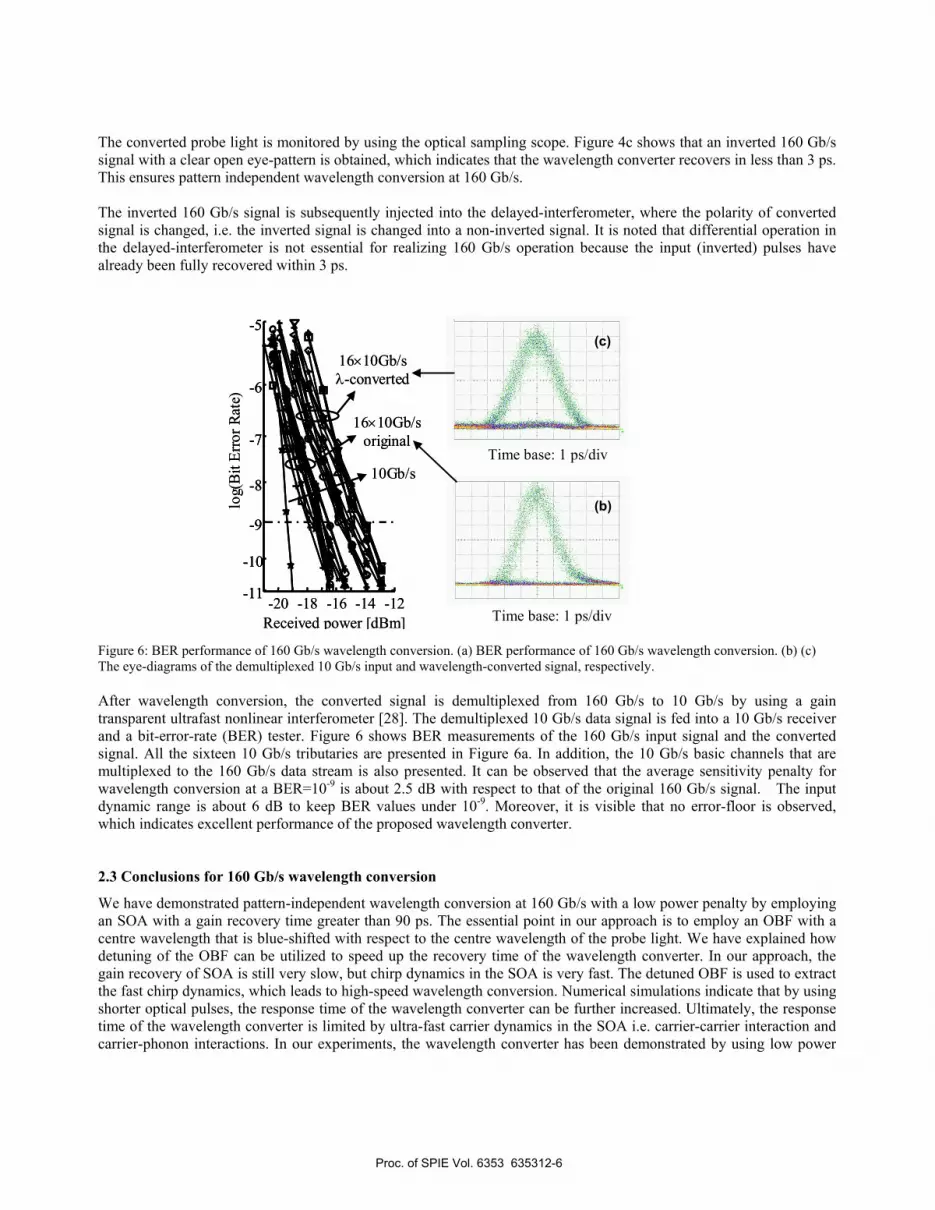
The converted probe light is monitored by using the optical sampling scope. Figure 4c shows that an inverted 160 Gb/s signal with a clear open eye-pattern is obtained, which indicates that the wavelength converter recovers in less than 3 ps. This ensures pattern independent wavelength conversion at 160 Gb/s. The inverted 160 Gb/s signal is subsequently injected into the delayed-interferometer, where the polarity of converted signal is changed, i.e. the inverted signal is changed into a non-inverted signal. It is noted that differential operation in the delayed-interferometer is not essential for realizing 160 Gb/s operation because the input (inverted) pulses have already been fully recovered within 3 ps. Figure 6: BER performance of 160 Gb/s wavelength conversion. (a) BER performance of 160 Gb/s wavelength conversion. (b) (c) The eye-diagrams of the demultiplexed 10 Gb/s input and wavelength-converted signal, respectively. After wavelength conversion, the converted signal is demultiplexed from 160 Gb/s to 10 Gb/s by using a gain transparent ultrafast nonlinear interferometer [28]. The demultiplexed 10 Gb/s data signal is fed into a 10 Gb/s receiver and a bit-error-rate (BER) tester. Figure 6 shows BER measurements of the 160 Gb/s input signal and the converted signal. All the sixteen 10 Gb/s tributaries are presented in Figure 6a. In addition, the 10 Gb/s basic channels that are multiplexed to the 160 Gb/s data stream is also presented. It can be observed that the average sensitivity penalty for wavelength conversion at a BER=10-9 is about 2.5 dB with respect to that of the original 160 Gb/s signal. The input dynamic range is about 6 dB to keep BER values under 10-9. Moreover, it is visible that no error-floor is observed, which indicates excellent performance of the proposed wavelength converter. 2.3 Conclusions for 160 Gb/s wavelength conversion
We have demonstrated pattern-independent wavelength conversion at 160 Gb/s with a low power penalty by employing an SOA with a gain recovery time greater than 90 ps. The essential point in our approach is to employ an OBF with a centre wavelength that is blue-shifted with respect to the centre wavelength of the probe light. We have explained how detuning of the OBF can be utilized to speed up the recovery time of the wavelength converter. In our approach, the gain recovery of SOA is still very slow, but chirp dynamics in the SOA is very fast. The detuned OBF is used to extract the fast chirp dynamics, which leads to high-speed wavelength conversion. Numerical simulations indicate that by using shorter optical pulses, the response time of the wavelength converter can be further increased. Ultimately, the response time of the wavelength converter is limited by ultra-fast carrier dynamics in the SOA i.e. carrier-carrier interaction and carrier-phonon interactions. In our experiments, the wavelength converter has been demonstrated by using low power
-20 -18 -16 -14 -12Received power [dBm]
log(
Bit
Erro
r Rat
e)
-11
-10
-9
-8
-7
-5
-6
16×10Gb/sλ-converted
16×10Gb/soriginal
10Gb/s
-20 -18 -16 -14 -12Received power [dBm]
log(
Bit
Erro
r Rat
e)
-11
-10
-9
-8
-7
-5
-6
-11
-10
-9
-8
-7
-5
-6
16×10Gb/sλ-converted
16×10Gb/soriginal
10Gb/s
Time base: 1 ps/div
Time base: 1 ps/div
(c)
(b)
Proc. of SPIE Vol. 6353 635312-6
optical pulses and commercially available fiber pigtailed components. The wavelength converter has a simple configuration and allows photonic integration.
3. ALL-OPTICAL ROUTING OF 80 GB/S DATA PACKETS In this section, firstly we introduce a monolithically integrated optical flip-flop, then we demonstrate that the integrated optical flip-flop is capable of controlling an SOA-based all-optical wavelength converter to route 80 Gb/s data packets all-optically, experimental proof is given. Finally this section is ended with conclusions. 3.1 All-optical flip-flop for all-optical packet switching
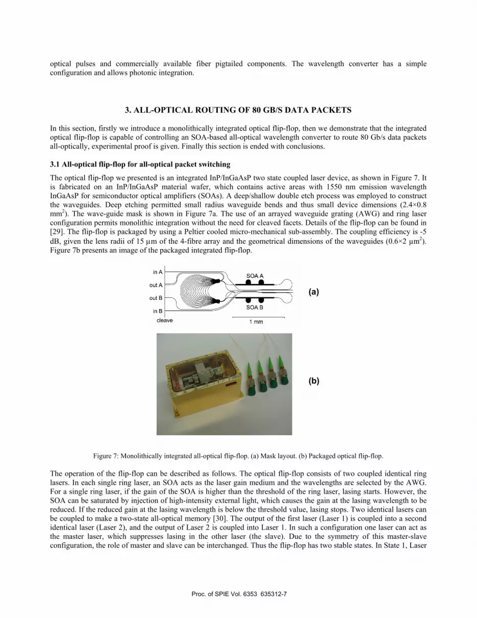
The optical flip-flop we presented is an integrated InP/InGaAsP two state coupled laser device, as shown in Figure 7. It is fabricated on an InP/InGaAsP material wafer, which contains active areas with 1550 nm emission wavelength InGaAsP for semiconductor optical amplifiers (SOAs). A deep/shallow double etch process was employed to construct the waveguides. Deep etching permitted small radius waveguide bends and thus small device dimensions (2.4×0.8 mm2). The wave-guide mask is shown in Figure 7a. The use of an arrayed waveguide grating (AWG) and ring laser configuration permits monolithic integration without the need for cleaved facets. Details of the flip-flop can be found in [29]. The flip-flop is packaged by using a Peltier cooled micro-mechanical sub-assembly. The coupling efficiency is -5 dB, given the lens radii of 15 µm of the 4-fibre array and the geometrical dimensions of the waveguides (0.6×2 µm2). Figure 7b presents an image of the packaged integrated flip-flop.
Figure 7: Monolithically integrated all-optical flip-flop. (a) Mask layout. (b) Packaged optical flip-flop. The operation of the flip-flop can be described as follows. The optical flip-flop consists of two coupled identical ring lasers. In each single ring laser, an SOA acts as the laser gain medium and the wavelengths are selected by the AWG. For a single ring laser, if the gain of the SOA is higher than the threshold of the ring laser, lasing starts. However, the SOA can be saturated by injection of high-intensity external light, which causes the gain at the lasing wavelength to be reduced. If the reduced gain at the lasing wavelength is below the threshold value, lasing stops. Two identical lasers can be coupled to make a two-state all-optical memory [30]. The output of the first laser (Laser 1) is coupled into a second identical laser (Laser 2), and the output of Laser 2 is coupled into Laser 1. In such a configuration one laser can act as the master laser, which suppresses lasing in the other laser (the slave). Due to the symmetry of this master-slave configuration, the role of master and slave can be interchanged. Thus the flip-flop has two stable states. In State 1, Laser
(a)
(b)
Proc. of SPIE Vol. 6353 635312-7

_JLJ LU L I LJ
1 is lasing, suppressing Laser 2, and then the flip-flop outputs CW light at wavelength λ1. Conversely, in State 2, Laser 2 is lasing, suppressing Laser 1, the flip-flop outputs CW light at wavelength λ2. To change states, lasing of the dominant laser is stopped by injecting external light into the dominant laser cavity to quench laser action. As a consequence, the suppressed laser could recover and become the dominant laser. 3.2 All-optical packet routing experiment
Our experimental setup that utilizes the monolithic integrated optical flop-flop for all-optical switching is shown in Figure 8a.
3dBMOD
1545.32nm
10 80 MuX
1.9 ps 10 Gb/s MLFRL
Integrated Optical Flip-flop
PC1
10 Gb/sPRBS 27-1
EDFA
5nmBPF
80 Gb/s transmitter
CW, λ1 or λ2 Optical sampling scope
80 10DeMuX
10 Gb/sReceiver
80 Gb/s receiver
Prec
PBS
SOA
1.4nm
All-optical wavelength converter (AOWC)
2 psPMF
PC2 PC3
BPF
PC4 PC5
PBS
λ1
λ2
λ1
λ2
5nmBPF
EDFA
Set ResetOptical pulses
Figure 8: (a) all-optical switching set-up. (b) Optical pulses for setting and resetting, and output from flip-flop that shows the switching between the two states. (c) Mask layout of integrated flip-flop. (d) Spectra of the two states of flip-flop The system under investigation consists of two parts: an integrated all-optical flip-flop and an all-optical wavelength converter. At the transmitter side, a 10-Gb/s 27−1 return-to-zero (RZ) pseudo random binary sequence (PRBS) data packet consisting of 1.9-ps optical pulses is multiplexed to 80-Gb/s by using passive fiber-based pulse interleavers. The 80 Gb/s data packets have duration of 35 ns and are separated by 15 ns of guard time. The data packets are combined with the CW light from the optical flip-flop, and simultaneously fed into the wavelength converter via a 3-dB coupler. The dashed box in Figure 8a shows the optical wavelength converter, which converts the wavelength of the data packet into the wavelength that outputs from the flip-flop. The wavelength converter is constructed by using commercially available fiber-pigtailed components. It is shown in [11] that this configuration allows error-free non-inverted wavelength conversion at 160 Gb/s. Both the data packet and CW output from the flip-flop are fed into the SOA to achieve inverted wavelength conversion based on cross-gain modulation. The SOA output power is equally divided over two branches via a 3-dB coupler. Each branch contains a 1.4 nm (FWHM) optical bandpass filter (OBF) with a central wavelength that is 1 nm blue-shifted with respect to the center wavelength of the flip-flop outputs. The 1 nm blue-side detuning is essential because the detuning of the OBF allows utilization of ultra-fast chirp dynamics in the SOA, and suppression of the slow gain recovery of the SOA. Thus the recovery time of the wavelength converter can be shortened to 3 ps, which ensures the pattern-independence of 80 Gb/s wavelength conversion [11]. The 3-dB coupler and two 1.4 nm OBFs act as an optical demultiplexer, and can be replaced by an integrated AWG. The central wavelengths of the OBFs are chosen such that in the upper branch, only light with wavelength λ1 can pass while in the lower branch, light
λ 1 λ 2
Set Reset
0 100 200 ns (b) (c)
(a)
(d) 1550 1560 1570 nm
λ1
λ2
Proc. of SPIE Vol. 6353 635312-8
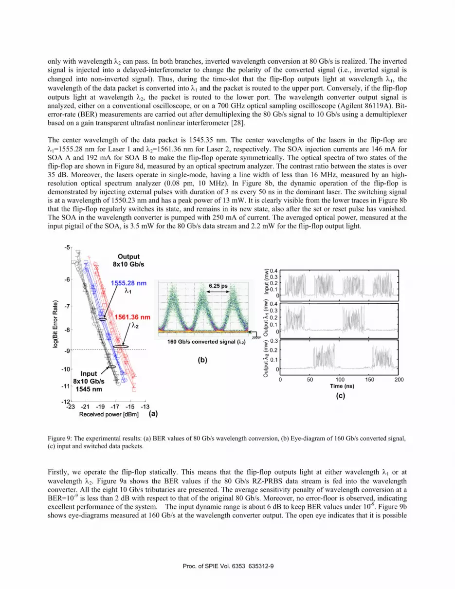
only with wavelength λ2 can pass. In both branches, inverted wavelength conversion at 80 Gb/s is realized. The inverted signal is injected into a delayed-interferometer to change the polarity of the converted signal (i.e., inverted signal is changed into non-inverted signal). Thus, during the time-slot that the flip-flop outputs light at wavelength λ1, the wavelength of the data packet is converted into λ1 and the packet is routed to the upper port. Conversely, if the flip-flop outputs light at wavelength λ2, the packet is routed to the lower port. The wavelength converter output signal is analyzed, either on a conventional oscilloscope, or on a 700 GHz optical sampling oscilloscope (Agilent 86119A). Bit-error-rate (BER) measurements are carried out after demultiplexing the 80 Gb/s signal to 10 Gb/s using a demultiplexer based on a gain transparent ultrafast nonlinear interferometer [28]. The center wavelength of the data packet is 1545.35 nm. The center wavelengths of the lasers in the flip-flop are λ1=1555.28 nm for Laser 1 and λ2=1561.36 nm for Laser 2, respectively. The SOA injection currents are 146 mA for SOA A and 192 mA for SOA B to make the flip-flop operate symmetrically. The optical spectra of two states of the flip-flop are shown in Figure 8d, measured by an optical spectrum analyzer. The contrast ratio between the states is over 35 dB. Moreover, the lasers operate in single-mode, having a line width of less than 16 MHz, measured by an high-resolution optical spectrum analyzer (0.08 pm, 10 MHz). In Figure 8b, the dynamic operation of the flip-flop is demonstrated by injecting external pulses with duration of 3 ns every 50 ns in the dominant laser. The switching signal is at a wavelength of 1550.23 nm and has a peak power of 13 mW. It is clearly visible from the lower traces in Figure 8b that the flip-flop regularly switches its state, and remains in its new state, also after the set or reset pulse has vanished. The SOA in the wavelength converter is pumped with 250 mA of current. The averaged optical power, measured at the input pigtail of the SOA, is 3.5 mW for the 80 Gb/s data stream and 2.2 mW for the flip-flop output light. Figure 9: The experimental results: (a) BER values of 80 Gb/s wavelength conversion, (b) Eye-diagram of 160 Gb/s converted signal, (c) input and switched data packets. Firstly, we operate the flip-flop statically. This means that the flip-flop outputs light at either wavelength λ1 or at wavelength λ2. Figure 9a shows the BER values if the 80 Gb/s RZ-PRBS data stream is fed into the wavelength converter. All the eight 10 Gb/s tributaries are presented. The average sensitivity penalty of wavelength conversion at a BER=10-9 is less than 2 dB with respect to that of the original 80 Gb/s. Moreover, no error-floor is observed, indicating excellent performance of the system. The input dynamic range is about 6 dB to keep BER values under 10-9. Figure 9b shows eye-diagrams measured at 160 Gb/s at the wavelength converter output. The open eye indicates that it is possible
-23 -21 -19 -17 -15 -13-12
-11
-10
-9
-8
-7
-6
-5
Received power [dBm]
log(
Bit
Erro
r Rat
e)
-23 -21 -19 -17 -15 -13-12
-11
-10
-9
-8
-7
-6
-5
Received power [dBm]
log(
Bit
Erro
r Rat
e)
Input 8x10 Gb/s 1545 nm
Output 8x10 Gb/s
1555.28 nm
1561.36 nm
λ1
λ2
6.25 ps
160 Gb/s converted signal (λ2)
00.10.20.30.4
00.10.20.30.4
0 50 100 150 200
0
0.1
0.2
0.3
Time (ns)
Out
put λ
2 (m
w)
Inpu
t (m
w)
Out
put λ
1 (m
w)
(a)
(b)
(c)
Proc. of SPIE Vol. 6353 635312-9

for the system to operate error free at 160 Gb/s. Furthermore, we demonstrate routing of 80 Gb/s data-packets by operating the flip-flop dynamically, as shown in Figure 9c. It is clearly visible that the input packets are routed to different ports when the flip-flop toggles between two states. 3.3 Conclusions for 80 Gb/s all-optical routing
We have demonstrated that a monolithically integrated optical flip-flop based on two coupled lasers is capable of controlling an optical wavelength converter to have error-free operation at 80 Gb/s data rate. An open eye suggests that also error-free operation at 160 Gb/s is possible. The system is capable of all-optically routing 80 Gb/s data packets with duration of 35 ns, separated by 15 ns of guard time.
4. CONCLUSIONS AND DISCUSSIONS We demonstrate all-optical routing of 80 Gb/s optical data packets by using a SOA-based optical wavelength converter and a monolithically integrated optical flip-flop. The routing is realized without using electronic control signal. The system is capable of all-optically routing 80 Gb/s data packets with duration of 35 ns, separated by 15 ns of guard time. The guard time between the packets is limited by the switching speed of the optical flip-flop, which is for this device approximately 2 ns. To reduce the switching time, an optical flip-flop can be formed by two coupled Mach-Zehnder interferometers. A hybrid-integrated version of this device with a switching time of less than 200 ps can be found in [31]. The switching time can also be reduced by employing micro-lasers, a switching time of less than 20 ps has been reported [32]. Employing such a device would lead to routing of the packets separated by a dramatically reduced guard time. Moreover, error-free SOA-based wavelength conversion has achieved at 320 Gb/s [33]. This suggests that this wavelength routing system could handle data rates up to at least 320 Gb/s.
ACKNOWLEDGEMENTS This work was funded by IST-LASAGNE (FP6-507509), STW EET6491 and the NRC photonics grant. The authors are indebted to Aragón Photonics for the loan of the high-resolution optical spectrum analyzer.
REFERENCES 1. D.J. Blumenthal, J.E. Bowers, L.Rau, et al., “Optical Signal Processing for Optical Packet Switching Networks”,
IEEE Opt. Comm., S23-S29, (2003). 2. H.J.S. Dorren, M.T. Hill, Y. Liu, N. Calabretta, A. Srivatsa, F.M. Huijskens, H. de Waardt and G.D. Khoe, “Optical
Packet Switching and Buffering by using all-Optical Signal Processing Methods”, J. Lightwave Techn. 21, 2-12 (2003).
3. M.T. Hill, A. Srivatsa, N. Calabretta, Y. Liu, H. de Waardt, G.D. Khoe, H.J.S. Dorren, “1×2 optical packet switch using all-optical header processing”, Electron. Lett. 37, 774-775, (2001).
4. F. Ramos, E. Kehayas, J. M. Martinez, R. Clavero, J. Marti, L. Stampoulidis, et al, “IST-LASAGNE: towards all-optical label swapping employing optical logic gates and optical flip-flops”, J. Lightwave Techn., 23, 2993-3011, (2005).
5. Y. Liu, E. Tangdiongga, M.T. Hill, J.H.C. van Zantvoort, E. Smalbrugge, T. de Vries, H. Binsma, Y.S. Oei, X.J.M. Leijtens, M.K. Smit, G. D. Khoe and H.J.S. Dorren," All-optical switching of 80 Gb/s data packets using a wavelength converter controlled by a monolithically integrated optical flip-flop", in Proceedings of 31th European Conference on Optical Communication (ECOC’2005), post-deadline, Th4.3.2, Glasgow, Scotland, Sept. 2005.
6. M. Takenaka, M. Raburn, K. Takeda, and Y. Nakano, “All-Optical Packet Switching by MMI-BLD Optical Flip-Flop”, in Proceedings of 2006 OFC/NFOEC, Paper OTHS3, Anaheim, California, USA, March 5-10, 2006.
Proc. of SPIE Vol. 6353 635312-10

7. P. K. A. Wai, L. Y. Chan, L. F. K. Lui, Lixin Xu, H. Y. Tam, and M. S. Demokan, “1×4 all-optical packet switch at 10 Gb/s,” IEEE Photon. Technol. Lett., 17, 1289-1291, (2005).
8. C. Guillemot et al, “Transparent Optical Packet Switching: The European ACTS KEOPS Project Approach”, J. Lightwave Technol. 16, 2117-2134 (1998).
9. D. Cotter, R. J. Manning, K. J. Blow, A. D. Ellis, A. E. Kelly, N. Nesset, I. D. Phillips, A. J. Poustie, and D. C. Rogers, “Nonlinear optics for high-speed digital information processing,” Science, 286, 1523-1528, (1999).
10. P. Bernasconi, L. Zhang, W. Yang, N. Sauer, L. L. Buhl, J. H. Sinsky, I.Kang, S. Chandrasekhar, D. T. Neilson: “Monolithically integrated 40-Gb/s switchable wavelength converter”, J. Lightwave Tech., 24, 71-75, (2006).
11. Y. Liu, E. Tangdiongga, Z. Li, S. Zhang, H. d. Waardt, G. D. Khoe and H.J.S. Dorren, “Error-free all-optical wavelength conversion at 160 Gb/s using a semiconductor optical amplifier and an optical bandpass filter,” J. Lightwave Tech. , 24, pp. 230-236, (2006).
12. Y. Liu, E. Tangdiongga, Z. Li, S. Zhang, H. d. Waardt, G. D. Khoe and H.J.S. Dorren, “80 Gb/s wavelength conversion using a semiconductor optical amplifier and an optical bandpass filter,” Electronics Letters, 41, pp. 487-489, (2005).
13. A.D. Ellis, A.E. Kelly, D. Nesset, D. Pitcher, D.G. Moodie and R. Kashyap: “Error free 100 Gb/s wavelength conversion using grating assisted cross-gain modulation in 2mm long semiconductor amplifier”, Electron. Lett., 34, 1958-1959, (1998).
14. H.Y. Yu, D. Mahgereftech, P.S. Cho and J. Goldhar: “Optimization of the frequency response of a semiconductor optical amplifier wavelength converter using a fiber bragg grating”, J. of Lightwave Technol., 17, 308-315, (1999).
15. Y. Dong, L. Lu, H. Wang and S. Xie: “Improving performance using waveguide filter and optimal probe and signal powers for all-optical wavelength conversion”, Proceedings of OFC’2000, TuF2, 69-71, Baltimore MD,USA, 5-10, March, 2000.
16. R. J. Manning, R.J. Manning, X. Yang, R.P. Webb, R. Giller, F.C. Garcia Gunning, A.D. Ellis, “The ‘Turbo-Switch’ - a Novel Technique to Increase the High-speed Response of SOAs for Wavelength Conversion,” in Proceedings of 2006 OFC/NFOEC, Paper OWS8, Anaheim, California, USA, March 5-10, 2006.
17. S. Nakamura, Y. Ueno and K. Tajima: “168-Gb/s all-optical wavelength conversion with a symmetric-Mach-Zehnder-Type switch”, IEEE Photo. Tech. Lett., 13, 1091-1093, (2001).
18. J. Leuthold, L. Moller, J. Jaques, S. Cabot, L. Zhang, P. Bernasconi, M. Cappuzzo, L. Gomez, E. Laskowski, E. Chen, A. Wong-Foy and A. Griffin: “160 Gb/s SOA all-optical wavelength converter and assessment of its regenerative properties”, Electron. Lett., 40, 554-555, (2004).
19. Y. Ueno, S. Nakamura and K. Tajima: “Nonlinear phase shifts induced by semiconductor optical amplifiers with control pulses at repetition frequencies in the 40–160-GHz range for use in ultrahigh-speed all-optical signal processing”, J. Opt. Soc. Am. B, 19, 2573-2589, (2002).
20. M.L. Nielsen and J. Mørk: “Increasing the modulation bandwidth of semiconductor-optical-amplifier-based switches by using optical filtering”, J. Opt. Soc. Am. B, 21, 1606-1619, (2004).
21. M. L. Nielsen, J. Mørk, R. Suzuki, J. Sakaguchi, and Y. Ueno, "Experimental and theoretical investigation of the impact of ultra-fast carrier dynamics on high-speed SOA-based all-optical switches," Opt. Express, 14, 331-347, (2006).
22. H. Chayett, S. Ben Ezra, N. Shachar, S. Tzadok, S. Tsadka and J. Leuthold: “Regenerative all-optical wavelength converter based on semiconductor optical amplifier and sharp frequency response,” in Proceedings of OFC2004, Ths2, USA, Feb. 2004.
23. M.L. Nielsen, B. Lavigne and B. Dagens: “Polarity-preserving SOA-based wavelength conversion at 40 Gb/s using bandpass filtering”, Electron. Lett., 39, 1334-1335, (2003).
24. J. Leuthold, D. M. Marom, S. Cabot, J. J. Jaques, R. Ryf and C. R. Giles: “All-optical wavelength conversion using a pulse reformatting optical filter”, J. of Lightwave Tech., 22, 186-192, (2004).
25. J. Mark and J. Mørk: “Subpicosecond gain dynamics in InGaAsP optical amplifiers: Experiment and theory”, Appl. Phys. Lett. , 61, 2281-2283, (1992).
26. Z. Li, J. Molina Vazquez, Y. Liu, E. Tangdiongga, S. Zhang, G.D. Khoe, H.J.S. Dorren and D. Lenstraa: “Performance analysis of 160 Gb/s wavelength converter based on a semiconductor optical amplifier and an optical bandpass filter”, in preparation for IEEE J. Quantum Electron.
27. X. Yang, D.Lenstra, G.D. Khoe and H.J.S. Dorren: “Rate equation model of nonlinear polarization rotation induced by ultrashort pulses in a semiconductor optical amplifier”, Optics Communications, 223, 169-179, (2003).
Proc. of SPIE Vol. 6353 635312-11

28. C. Schubert, S. Diez, J. Berger, R. Ludwig, U. Feiste, H. G. Weber, G. Toptchiyski, K. Petermann and V. Krajinovic: “160-Gb/s all-optical demultiplexing using a gain- transparent ultrafast-nonlinear interferometer (GT-UNI)”, IEEE Photo. Tech. Lett., 13, 475-477, (2001).
29. M.T. Hill, H.J.S. Dorren, X.J.M. Leijtens, J. H. den Besten, T. de Vries, J.H.C. van Zantvoort, et al, “Integrated two-state AWG-based multiwavelength laser”, IEEE Photonics Technology Letters, 17, 956-958, (2005).
30. M. T. Hill, H. de Waardt, G. D. Khoe and H. J. S. Dorren “All-optical flip-flop based on coupled laser diodes,” IEEE Journal of Quantum Electron. 37, 405-413, (2001).
31. R. McDougall, Y. Liu, G. Maxwell, M. T. Hill, R. Harmon, S. Zhang, L. Rivers, F.M. Huijskens, A. Poustie and H.J.S. Dorren, “Hybrid Integrated, All-optical Flip-flop Memory Element for Optical Packet Networks”, accepted by Proceedings of ECOC2006, Th1.4.5, Cannes, France, Sept., 2006.
32. M.T. Hill, H.J.S. Dorren, T. de Vries, X.J.M. Leijtens, J.H. den Besten, B. Smallbrugge, S. Oei, J.J.M. Binsma, G.D. Khoe, M.K. Smit, “A fast low power optical memory based on coupled micro-ring lasers”, Nature 432, nr. 7014, pp. 206-209, (2004).
33. Y. Liu, E. Tangdiongga, Z. Li, H. de Waardt, A. M. J. Koonen, Xuewen Shu, Ian Bennion, G.D. Khoe and H.J.S. Dorren,"Error-free 320 Gb/s SOA-based Wavelength Conversion using Optical Filtering", in Proceedings of 2006 OFC/NFOEC, post-deadline paper, PDP28, Anaheim, California, USA, March, 2006.
Proc. of SPIE Vol. 6353 635312-12
Related Documents