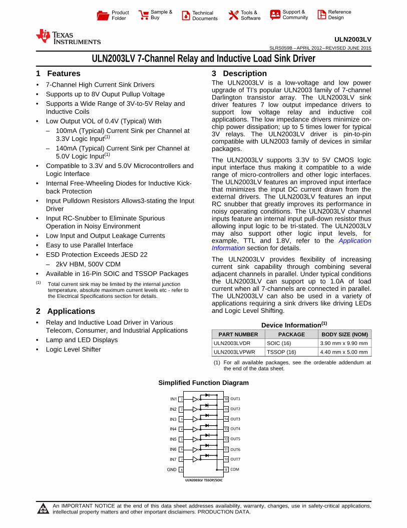
ULN2003LV TSSOP/SOIC IN1 IN2 IN3 IN4 IN5 IN6 IN7 GND OUT2 OUT3 OUT5 OUT6 OUT7 COM OUT1 OUT4 1 2 3 4 5 6 7 8 16 15 14 13 12 11 10 9 Product Folder Sample & Buy Technical Documents Tools & Software Support & Community Reference Design ULN2003LV SLRS059B – APRIL 2012 – REVISED JUNE 2015 ULN2003LV 7-Channel Relay and Inductive Load Sink Driver 1 Features 3 Description The ULN2003LV is a low-voltage and low power 1• 7-Channel High Current Sink Drivers upgrade of TI’s popular ULN2003 family of 7-channel • Supports up to 8V Ouput Pullup Voltage Darlington transistor array. The ULN2003LV sink • Supports a Wide Range of 3V-to-5V Relay and driver features 7 low output impedance drivers to Inductive Coils support low voltage relay and inductive coil applications. The low impedance drivers minimize on- • Low Output VOL of 0.4V (Typical) With chip power dissipation; up to 5 times lower for typical – 100mA (Typical) Current Sink per Channel at 3V relays. The ULN2003LV driver is pin-to-pin 3.3V Logic Input (1) compatible with ULN2003 family of devices in similar – 140mA (Typical) Current Sink per Channel at packages. 5.0V Logic Input (1) The ULN2003LV supports 3.3V to 5V CMOS logic • Compatible to 3.3V and 5.0V Microcontrollers and input interface thus making it compatible to a wide Logic Interface range of micro-controllers and other logic interfaces. The ULN2003LV features an improved input interface • Internal Free-Wheeling Diodes for Inductive Kick- that minimizes the input DC current drawn from the back Protection external drivers. The ULN2003LV features an input • Input Pulldown Resistors Allows3-stating the Input RC snubber that greatly improves its performance in Driver noisy operating conditions. The ULN2003LV channel • Input RC-Snubber to Eliminate Spurious inputs feature an internal input pull-down resistor thus allowing input logic to be tri-stated. The ULN2003LV Operation in Noisy Environment may also support other logic input levels, for • Low Input and Output Leakage Currents example, TTL and 1.8V, refer to the Application • Easy to use Parallel Interface Information section for details. • ESD Protection Exceeds JESD 22 The ULN2003LV provides flexibility of increasing – 2kV HBM, 500V CDM current sink capability through combining several • Available in 16-Pin SOIC and TSSOP Packages adjacent channels in parallel. Under typical conditions the ULN2003LV can support up to 1.0A of load (1) Total current sink may be limited by the internal junction current when all 7-channels are connected in parallel. temperature, absolute maximum current levels etc - refer to the Electrical Specifications section for details. The ULN2003LV can also be used in a variety of applications requiring a sink drivers like driving LEDs and Logic Level Shifting. 2 Applications • Relay and Inductive Load Driver in Various Device Information (1) Telecom, Consumer, and Industrial Applications PART NUMBER PACKAGE BODY SIZE (NOM) • Lamp and LED Displays ULN2003LVDR SOIC (16) 3.90 mm x 9.90 mm • Logic Level Shifter ULN2003LVPWR TSSOP (16) 4.40 mm x 5.00 mm (1) For all available packages, see the orderable addendum at the end of the data sheet. Simplified Function Diagram 1 An IMPORTANT NOTICE at the end of this data sheet addresses availability, warranty, changes, use in safety-critical applications, intellectual property matters and other important disclaimers. PRODUCTION DATA.

Welcome message from author
This document is posted to help you gain knowledge. Please leave a comment to let me know what you think about it! Share it to your friends and learn new things together.
Transcript
ULN2003LV TSSOP/SOIC
IN1
IN2
IN3
IN4
IN5
IN6
IN7
GND
OUT2
OUT3
OUT5
OUT6
OUT7
COM
OUT1
OUT4
1
2
3
4
5
6
7
8
16
15
14
13
12
11
10
9
Product
Folder
Sample &Buy
Technical
Documents
Tools &
Software
Support &Community
ReferenceDesign
ULN2003LVSLRS059B –APRIL 2012–REVISED JUNE 2015
ULN2003LV 7-Channel Relay and Inductive Load Sink Driver1 Features 3 Description
The ULN2003LV is a low-voltage and low power1• 7-Channel High Current Sink Drivers
upgrade of TI’s popular ULN2003 family of 7-channel• Supports up to 8V Ouput Pullup Voltage Darlington transistor array. The ULN2003LV sink• Supports a Wide Range of 3V-to-5V Relay and driver features 7 low output impedance drivers to
Inductive Coils support low voltage relay and inductive coilapplications. The low impedance drivers minimize on-• Low Output VOL of 0.4V (Typical) Withchip power dissipation; up to 5 times lower for typical– 100mA (Typical) Current Sink per Channel at 3V relays. The ULN2003LV driver is pin-to-pin
3.3V Logic Input(1)compatible with ULN2003 family of devices in similar
– 140mA (Typical) Current Sink per Channel at packages.5.0V Logic Input(1)
The ULN2003LV supports 3.3V to 5V CMOS logic• Compatible to 3.3V and 5.0V Microcontrollers and input interface thus making it compatible to a wide
Logic Interface range of micro-controllers and other logic interfaces.The ULN2003LV features an improved input interface• Internal Free-Wheeling Diodes for Inductive Kick-that minimizes the input DC current drawn from theback Protectionexternal drivers. The ULN2003LV features an input• Input Pulldown Resistors Allows3-stating the Input RC snubber that greatly improves its performance in
Driver noisy operating conditions. The ULN2003LV channel• Input RC-Snubber to Eliminate Spurious inputs feature an internal input pull-down resistor thus
allowing input logic to be tri-stated. The ULN2003LVOperation in Noisy Environmentmay also support other logic input levels, for• Low Input and Output Leakage Currentsexample, TTL and 1.8V, refer to the Application
• Easy to use Parallel Interface Information section for details.• ESD Protection Exceeds JESD 22
The ULN2003LV provides flexibility of increasing– 2kV HBM, 500V CDM current sink capability through combining several
• Available in 16-Pin SOIC and TSSOP Packages adjacent channels in parallel. Under typical conditionsthe ULN2003LV can support up to 1.0A of load(1) Total current sink may be limited by the internal junctioncurrent when all 7-channels are connected in parallel.temperature, absolute maximum current levels etc - refer to
the Electrical Specifications section for details. The ULN2003LV can also be used in a variety ofapplications requiring a sink drivers like driving LEDsand Logic Level Shifting.2 Applications
• Relay and Inductive Load Driver in Various Device Information(1)Telecom, Consumer, and Industrial Applications PART NUMBER PACKAGE BODY SIZE (NOM)
• Lamp and LED Displays ULN2003LVDR SOIC (16) 3.90 mm x 9.90 mm• Logic Level Shifter ULN2003LVPWR TSSOP (16) 4.40 mm x 5.00 mm
(1) For all available packages, see the orderable addendum atthe end of the data sheet.
Simplified Function Diagram
1
An IMPORTANT NOTICE at the end of this data sheet addresses availability, warranty, changes, use in safety-critical applications,intellectual property matters and other important disclaimers. PRODUCTION DATA.
ULN2003LVSLRS059B –APRIL 2012–REVISED JUNE 2015 www.ti.com
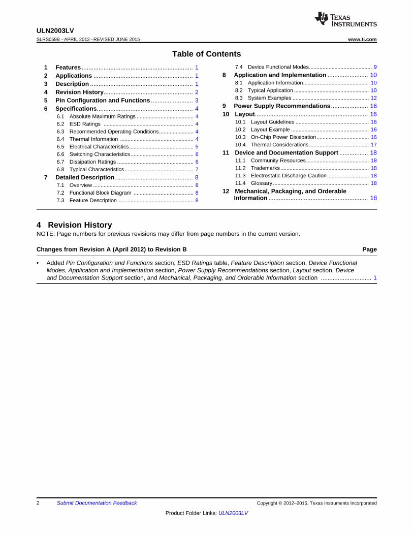
Table of Contents7.4 Device Functional Modes.......................................... 91 Features .................................................................. 1
8 Application and Implementation ........................ 102 Applications ........................................................... 18.1 Application Information............................................ 103 Description ............................................................. 18.2 Typical Application .................................................. 104 Revision History..................................................... 28.3 System Examples ................................................... 125 Pin Configuration and Functions ......................... 3
9 Power Supply Recommendations ...................... 166 Specifications......................................................... 410 Layout................................................................... 166.1 Absolute Maximum Ratings ...................................... 4
10.1 Layout Guidelines ................................................. 166.2 ESD Ratings ............................................................ 410.2 Layout Example .................................................... 166.3 Recommended Operating Conditions....................... 410.3 On-Chip Power Dissipation................................... 166.4 Thermal Information ................................................. 410.4 Thermal Considerations ........................................ 176.5 Electrical Characteristics........................................... 5
11 Device and Documentation Support ................. 186.6 Switching Characteristics .......................................... 611.1 Community Resources.......................................... 186.7 Dissipation Ratings ................................................... 611.2 Trademarks ........................................................... 186.8 Typical Characteristics .............................................. 711.3 Electrostatic Discharge Caution............................ 187 Detailed Description .............................................. 811.4 Glossary ................................................................ 187.1 Overview ................................................................... 8
12 Mechanical, Packaging, and Orderable7.2 Functional Block Diagram ........................................ 8Information ........................................................... 187.3 Feature Description .................................................. 8
4 Revision HistoryNOTE: Page numbers for previous revisions may differ from page numbers in the current version.
Changes from Revision A (April 2012) to Revision B Page
• Added Pin Configuration and Functions section, ESD Ratings table, Feature Description section, Device FunctionalModes, Application and Implementation section, Power Supply Recommendations section, Layout section, Deviceand Documentation Support section, and Mechanical, Packaging, and Orderable Information section .............................. 1
2 Submit Documentation Feedback Copyright © 2012–2015, Texas Instruments Incorporated
Product Folder Links: ULN2003LV

IN1
IN2
IN3
IN4
IN5
IN6
IN7
GND
OUT2
OUT3
OUT5
OUT6
OUT7
COM
OUT1
OUT4
1
2
3
4
5
6
7
8
16
15
14
13
12
11
10
9
16-Pin
SOIC/TSSOP
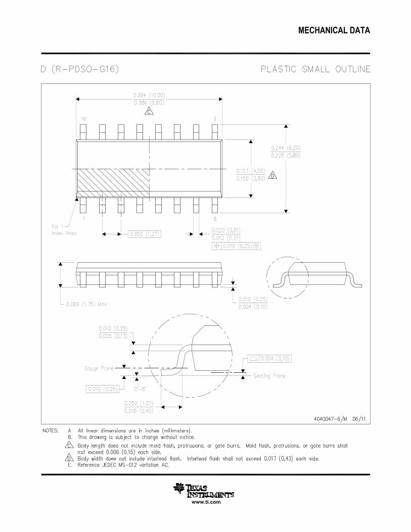
ULN2003LVwww.ti.com SLRS059B –APRIL 2012–REVISED JUNE 2015
5 Pin Configuration and Functions
D or PW Package16-Pin SOIC or TSSOP
Top View
Pin FunctionsPIN
TYPE DESCRIPTIONNAME NO.IN1 1 InputIN2 2 InputIN3 3 InputIN4 4 Input Logic Input Pins IN1 through IN7IN5 5 InputIN6 6 InputIN7 7 InputGND 8 Ground Ground Reference PinCOM 9 Output Internal Free-Wheeling Diode Common Cathode PinOUT7 10 OutputOUT6 11 OutputOUT5 12 OutputOUT4 13 Output Channel Output Pins OUT7 through OUT1OUT3 14 OutputOUT2 15 OutputOUT1 16 Output
Copyright © 2012–2015, Texas Instruments Incorporated Submit Documentation Feedback 3
Product Folder Links: ULN2003LV

ULN2003LVSLRS059B –APRIL 2012–REVISED JUNE 2015 www.ti.com
6 Specifications
6.1 Absolute Maximum RatingsSpecified at TJ = –40°C to 125°C unless otherwise noted. (1)
MIN MAX UNITVIN Pins IN1- IN7 to GND voltage –0.3 5.5 VVOUT Pins OUT1 – OUT7 to GND voltage 8 VVCOM Pin COM to GND voltage 8 V
Maximum GND-pin continuous current (TJ > +125°C) 700 mAIGND Maximum GND-pin continuous current (TJ < +100°C) 1.0 A
16 Pin - SOIC 0.58 WPD Total device power dissipation at TA = 85°C
16 Pin -TSSOP 0.45 WTA Operating free-air ambient temperature –40 85 °CTJ Operating virtual junction temperature –55 150 °CTstg Storage temperature –55 150 °C
(1) Stresses beyond those listed under Absolute Maximum Ratings may cause permanent damage to the device. These are stress ratingsonly, which do not imply functional operation of the device at these or any other conditions beyond those indicated under RecommendedOperating Conditions. Exposure to absolute-maximum-rated conditions for extended periods may affect device reliability.
6.2 ESD RatingsVALUE UNIT
Human body model (HBM), per ANSI/ESDA/JEDEC JS-001 (1) ±2000ElectrostaticV(ESD) Vdischarge Charged-device model (CDM), per JEDEC specification JESD22-C101 (2) ±500
(1) JEDEC document JEP155 states that 500-V HBM allows safe manufacturing with a standard ESD control process.(2) JEDEC document JEP157 states that 250-V CDM allows safe manufacturing with a standard ESD control process.
6.3 Recommended Operating Conditionsover operating free-air temperature range (unless otherwise noted)
MIN MAX UNIT
VOUT Channel off-state output pullup voltage 8 V
VCOM COM pin voltage 8 V
VINx = 3.3 V 100 (1)
IOUT(ON) Per channel continuous sink current mAVINx = 5.0 V 140 (1)
TJ Operating junction temperature –40 125 ºC
(1) Refer to Absolute Maximum Ratings for TJ dependent absolute maximum GND-pin current
6.4 Thermal InformationULN2003LV
THERMAL METRIC (1) D (SOIC) PW (TSSOP) UNIT16 PINS 16 PINS
RθJA Junction-to-ambient thermal resistance 112 142 °C/WRθJC(top) Junction-to-case (top) thermal resistance 69 74 °C/WRθJB Junction-to-board thermal resistance 69 87 °C/WψJT Junction-to-top characterization parameter 33 22 °C/WψJB Junction-to-board characterization parameter 69 87 °C/W
(1) For more information about traditional and new thermal metrics, see the Semiconductor and IC Package Thermal Metrics applicationreport, SPRA953.
4 Submit Documentation Feedback Copyright © 2012–2015, Texas Instruments Incorporated
Product Folder Links: ULN2003LV
ULN2003LVwww.ti.com SLRS059B –APRIL 2012–REVISED JUNE 2015
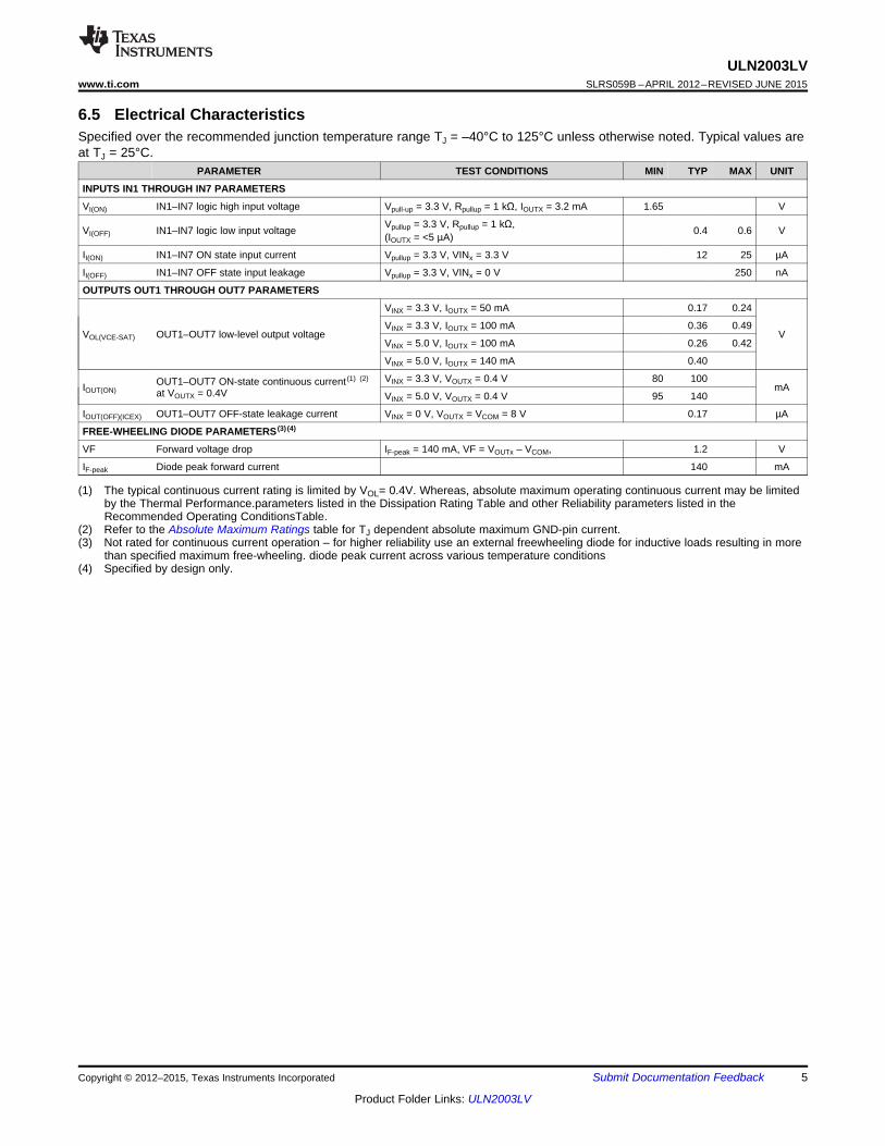
6.5 Electrical CharacteristicsSpecified over the recommended junction temperature range TJ = –40°C to 125°C unless otherwise noted. Typical values areat TJ = 25°C.
PARAMETER TEST CONDITIONS MIN TYP MAX UNIT
INPUTS IN1 THROUGH IN7 PARAMETERS
VI(ON) IN1–IN7 logic high input voltage Vpull-up = 3.3 V, Rpullup = 1 kΩ, IOUTX = 3.2 mA 1.65 V
Vpullup = 3.3 V, Rpullup = 1 kΩ,VI(OFF) IN1–IN7 logic low input voltage 0.4 0.6 V(IOUTX = <5 µA)
II(ON) IN1–IN7 ON state input current Vpullup = 3.3 V, VINx = 3.3 V 12 25 µA
II(OFF) IN1–IN7 OFF state input leakage Vpullup = 3.3 V, VINx = 0 V 250 nA
OUTPUTS OUT1 THROUGH OUT7 PARAMETERS
VINX = 3.3 V, IOUTX = 50 mA 0.17 0.24
VINX = 3.3 V, IOUTX = 100 mA 0.36 0.49VOL(VCE-SAT) OUT1–OUT7 low-level output voltage V
VINX = 5.0 V, IOUTX = 100 mA 0.26 0.42
VINX = 5.0 V, IOUTX = 140 mA 0.40
VINX = 3.3 V, VOUTX = 0.4 V 80 100OUT1–OUT7 ON-state continuous current (1) (2)IOUT(ON) mAat VOUTX = 0.4V VINX = 5.0 V, VOUTX = 0.4 V 95 140
IOUT(OFF)(ICEX) OUT1–OUT7 OFF-state leakage current VINX = 0 V, VOUTX = VCOM = 8 V 0.17 µA
FREE-WHEELING DIODE PARAMETERS (3) (4)
VF Forward voltage drop IF-peak = 140 mA, VF = VOUTx – VCOM, 1.2 V
IF-peak Diode peak forward current 140 mA
(1) The typical continuous current rating is limited by VOL= 0.4V. Whereas, absolute maximum operating continuous current may be limitedby the Thermal Performance.parameters listed in the Dissipation Rating Table and other Reliability parameters listed in theRecommended Operating ConditionsTable.
(2) Refer to the Absolute Maximum Ratings table for TJ dependent absolute maximum GND-pin current.(3) Not rated for continuous current operation – for higher reliability use an external freewheeling diode for inductive loads resulting in more
than specified maximum free-wheeling. diode peak current across various temperature conditions(4) Specified by design only.
Copyright © 2012–2015, Texas Instruments Incorporated Submit Documentation Feedback 5
Product Folder Links: ULN2003LV
ULN2003LVSLRS059B –APRIL 2012–REVISED JUNE 2015 www.ti.com
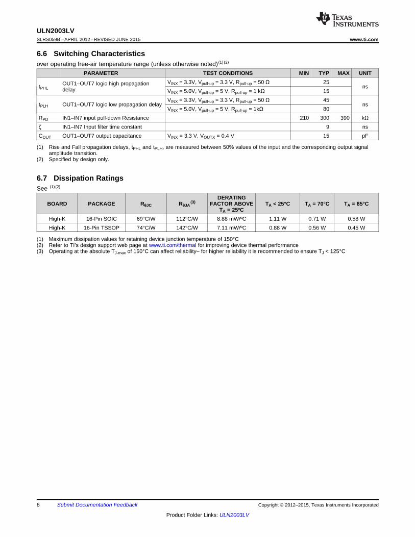
6.6 Switching Characteristicsover operating free-air temperature range (unless otherwise noted) (1) (2)
PARAMETER TEST CONDITIONS MIN TYP MAX UNITVINX = 3.3V, Vpull-up = 3.3 V, Rpull-up = 50 Ω 25OUT1–OUT7 logic high propagationtPHL nsdelay VINX = 5.0V, Vpull-up = 5 V, Rpull-up = 1 kΩ 15VINX = 3.3V, Vpull-up = 3.3 V, Rpull-up = 50 Ω 45
tPLH OUT1–OUT7 logic low propagation delay nsVINX = 5.0V, Vpull-up = 5 V, Rpull-up = 1kΩ 80
RPD IN1–IN7 input pull-down Resistance 210 300 390 kΩζ IN1–IN7 Input filter time constant 9 nsCOUT OUT1–OUT7 output capacitance VINX = 3.3 V, VOUTX = 0.4 V 15 pF
(1) Rise and Fall propagation delays, tPHL and tPLH, are measured between 50% values of the input and the corresponding output signalamplitude transition.
(2) Specified by design only.
6.7 Dissipation RatingsSee (1) (2)
DERATINGBOARD PACKAGE RθJC RθJA
(3) FACTOR ABOVE TA < 25°C TA = 70°C TA = 85°CTA = 25ºC
High-K 16-Pin SOIC 69°C/W 112°C/W 8.88 mW/ºC 1.11 W 0.71 W 0.58 WHigh-K 16-Pin TSSOP 74°C/W 142°C/W 7.11 mW/ºC 0.88 W 0.56 W 0.45 W
(1) Maximum dissipation values for retaining device junction temperature of 150°C(2) Refer to TI’s design support web page at www.ti.com/thermal for improving device thermal performance(3) Operating at the absolute TJ-max of 150°C can affect reliability– for higher reliability it is recommended to ensure TJ < 125°C
6 Submit Documentation Feedback Copyright © 2012–2015, Texas Instruments Incorporated
Product Folder Links: ULN2003LV

ULN2003LVwww.ti.com SLRS059B –APRIL 2012–REVISED JUNE 2015
6.8 Typical CharacteristicsTA = +25ºC
Figure 1. Load Current 1-Channel; VOL=0.4V Figure 2. Load Current 7-Channels in Parallel; VOL=0.4V
Figure 3. VOL versus IOUT VIN = 1.8V, 3.3V, 5.0V Figure 4. VOL versus IOUT 2-Channels in Parallel; VOL=0.4V
Figure 5. Freewheeling Diode VF vs IF
Copyright © 2012–2015, Texas Instruments Incorporated Submit Documentation Feedback 7
Product Folder Links: ULN2003LV
INX
ESD ESD
OUTX
RIN=3kQ
Pull-down
300kQ
CIN= 9pF
COM
NFET
RC Filter/Snubber
ULN2003LVSLRS059B –APRIL 2012–REVISED JUNE 2015 www.ti.com
7 Detailed Description
7.1 OverviewULN2003LV device is a seven-channel, low-side NMOS driver capable of driving 100-mA load with 3-V inputdrive voltage through each channel. This device can drive low voltage can drive low-voltage relays, LEDs orresistive loads. The ULN2003LV supports 3.3-V to 5-V CMOS logic input interface thus making it compatible to awide range of micro-controllers and other logic interfaces. The ULN2003LV features an improved input interfacethat minimizes the input DC current drawn from the external drivers. The ULN2003LV features an input RCsnubber that greatly improves its performance in noisy operating conditions. The ULN2003LV channel inputsfeature an internal input pulldown resistor thus allowing input logic to be tri-stated. The ULN2003LV may alsosupport other logic input levels, for example, TTL and 1.8 V.
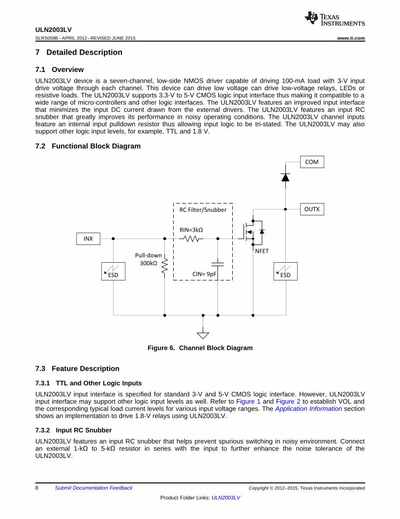
7.2 Functional Block Diagram
Figure 6. Channel Block Diagram
7.3 Feature Description
7.3.1 TTL and Other Logic InputsULN2003LV input interface is specified for standard 3-V and 5-V CMOS logic interface. However, ULN2003LVinput interface may support other logic input levels as well. Refer to Figure 1 and Figure 2 to establish VOL andthe corresponding typical load current levels for various input voltage ranges. The Application Information sectionshows an implementation to drive 1.8-V relays using ULN2003LV.
7.3.2 Input RC SnubberULN2003LV features an input RC snubber that helps prevent spurious switching in noisy environment. Connectan external 1-kΩ to 5-kΩ resistor in series with the input to further enhance the noise tolerance of theULN2003LV.
8 Submit Documentation Feedback Copyright © 2012–2015, Texas Instruments Incorporated
Product Folder Links: ULN2003LV
ULN2003LVwww.ti.com SLRS059B –APRIL 2012–REVISED JUNE 2015
Feature Description (continued)7.3.3 High-Impedance Input DriversULN2003LV features a 300-kΩ input pulldown resistor. The presence of this resistor allows the input drivers tobe tri-stated. When a high-impedance driver is connected to a channel input the ULN2003LV detects the channelinput as a low-level input and remains in the OFF position. The input RC snubber helps improve noise tolerancewhen input drivers are in the high-impedance state.
7.4 Device Functional ModesAs shown in Figure 6, each output of the ULN2003LV features an internal free-wheeling diode connected in acommon-cathode configuration at the COM pin. The ULN2003LV provides flexibility of increasing current sinkcapability through combining several adjacent channels in parallel. Under typical conditions the ULN2003LV cansupport up to 1.0 A of load current when all 7-channels are connected in parallel. The ULN2003LV can also beused in a variety of other applications requiring a sink drivers.
Table 1. ULN2003LV Function Table (1)
INPUT (IN1 – IN7) OUTPUT (OUT1–OUT7)L ZH LZ Z
(1) L = Low-level (GND); H= High-level; Z= High-impedance
Copyright © 2012–2015, Texas Instruments Incorporated Submit Documentation Feedback 9
Product Folder Links: ULN2003LV
ULN2003LV
IN3
IN4
OUT1
OUT2
OUT3
OUT4
IN5
IN6
IN7
GND
OUT5
OUT6
OUT7
COM
IN1
IN2
VSUP Level Shift Supply(Up to 8V)
Logic Inputs
(1.8V to 5V)
OUT1_VSUP
OUT2_VSUP
OUT3_VSUP
OUT4_VSUP
OUT5_VSUP
OUT6_VSUP
OUT7_VSUP
ULN2003LVSLRS059B –APRIL 2012–REVISED JUNE 2015 www.ti.com
8 Application and Implementation
NOTEInformation in the following applications sections is not part of the TI componentspecification, and TI does not warrant its accuracy or completeness. TI’s customers areresponsible for determining suitability of components for their purposes. Customers shouldvalidate and test their design implementation to confirm system functionality.
8.1 Application InformationThe typical application of the ULN2003LV is a sink driver. The ULN2003LV provides a low-impedance path toGND for driving external peripherals or open-drain signals. If all 7 channels are tied together, the ULN2003 cansink up to 1 A of current in these applications
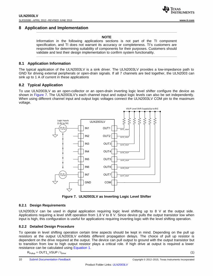
8.2 Typical ApplicationTo use ULN2003LV as an open-collector or an open-drain inverting logic level shifter configure the device asshown in Figure 7. The ULN2003LV’s each channel input and output logic levels can also be set independently.When using different channel input and output logic voltages connect the ULN2003LV COM pin to the maximumvoltage.
Figure 7. ULN2003LV as Inverting Logic Level Shifter
8.2.1 Design RequirementsULN2003LV can be used in digital application requiring logic level shifting up to 8 V at the output side.Applications requiring a level shift operation from 1.8 V to 8 V. Since device pulls the output transistor low wheninput is high, this configuration is useful for applications requiring inverting logic with the level shifting operation.
8.2.2 Detailed Design ProcedureTo operate in level shifting operation certain time aspects should be kept in mind. Depending on the pull upresistors at the output ULN2003LV exhibits different propagation delays. The choice of pull up resistor isdependent on the drive required at the output. The device can pull output to ground with the output transistor butto transition from low to high output resistor plays a critical role. If high drive at output is required a lowerresistance can be calculated using Equation 1.
RPullup = OUT1_VSUP / IDrive (1)
10 Submit Documentation Feedback Copyright © 2012–2015, Texas Instruments Incorporated
Product Folder Links: ULN2003LV

ULN2003LVwww.ti.com SLRS059B –APRIL 2012–REVISED JUNE 2015
Typical Application (continued)For example, a drive of 5 mA is required at the output for 1.8-V to 5-V translation application.
RPullup = OUT1_VSUP / IDrive = 5/0.005 =1 K (2)
8.2.3 Application Curve
Figure 8. ULN2003LV Iref vs VOUTx
Copyright © 2012–2015, Texas Instruments Incorporated Submit Documentation Feedback 11
Product Folder Links: ULN2003LV
ULN2003LV
IN3
IN4
OUT1
OUT2
OUT3
OUT4
IN5
IN6
IN7
GND
OUT5
OUT6
OUT7
COM
IN1
IN2
Logic Inputs
(1.8V to 5V)
VSUP_MAX
VSUP1
VSUP2
VSUP3
VSUP_MAX
VSUP_MAX = Max of VSUP1, VSUP2, VSUP3 – VF
VF = Diode forward drop@ Total ground-pin current
ULN2003LVSLRS059B –APRIL 2012–REVISED JUNE 2015 www.ti.com
8.3 System Examples
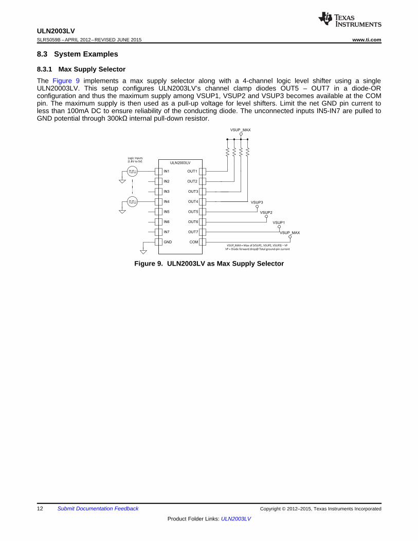
8.3.1 Max Supply SelectorThe Figure 9 implements a max supply selector along with a 4-channel logic level shifter using a singleULN20003LV. This setup configures ULN2003LV’s channel clamp diodes OUT5 – OUT7 in a diode-ORconfiguration and thus the maximum supply among VSUP1, VSUP2 and VSUP3 becomes available at the COMpin. The maximum supply is then used as a pull-up voltage for level shifters. Limit the net GND pin current toless than 100mA DC to ensure reliability of the conducting diode. The unconnected inputs IN5-IN7 are pulled toGND potential through 300kΩ internal pull-down resistor.
Figure 9. ULN2003LV as Max Supply Selector
12 Submit Documentation Feedback Copyright © 2012–2015, Texas Instruments Incorporated
Product Folder Links: ULN2003LV
ULN2003LV
IN3
IN4
OUT1
OUT2
OUT3
OUT4
IN5
IN6
IN7
GND
OUT5
OUT6
OUT7
COM
IN1
IN2
VSUP LED Supply(Up to 8V)
R1
OUT7
VSUP
VSUP
IRE
F7
VIN (Up to 5.5V)
OUT7
R1 = (VIN-VOUT7)/IREF7Use plot to estimate VOUT7 for the desired IREF7
ULN2003LVwww.ti.com SLRS059B –APRIL 2012–REVISED JUNE 2015
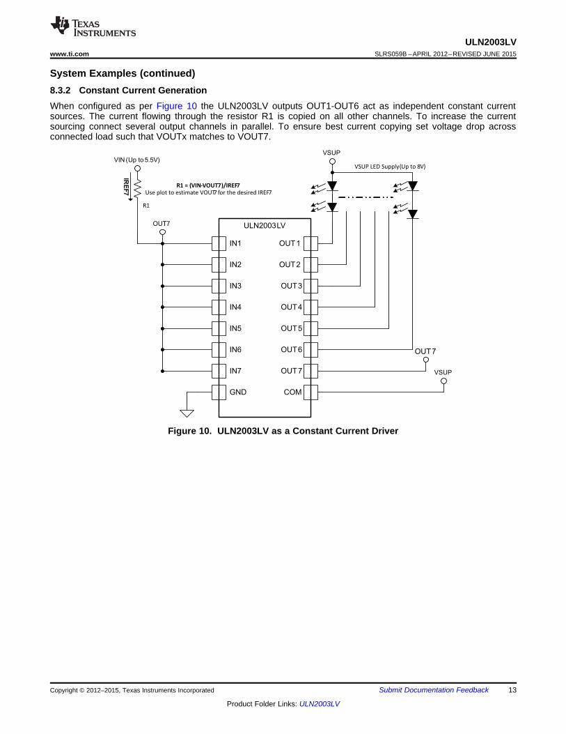
System Examples (continued)8.3.2 Constant Current GenerationWhen configured as per Figure 10 the ULN2003LV outputs OUT1-OUT6 act as independent constant currentsources. The current flowing through the resistor R1 is copied on all other channels. To increase the currentsourcing connect several output channels in parallel. To ensure best current copying set voltage drop acrossconnected load such that VOUTx matches to VOUT7.
Figure 10. ULN2003LV as a Constant Current Driver
Copyright © 2012–2015, Texas Instruments Incorporated Submit Documentation Feedback 13
Product Folder Links: ULN2003LV

ULN2003LV
IN3
IN4
OUT1
OUT2
OUT3
OUT4
IN5
IN6
IN7
GND
OUT5
OUT6
OUT7
COM
IN1
IN2
Logic Inputs
(1.8V to 5V)
VSUP
IN1 NOR IN2 IN3 NOR IN4 VSUP
VSUP
IN1 NOR IN2 NOR IN3
ULN2003LV
IN3
IN4
OUT1
OUT2
OUT3
OUT4
IN5
IN6
IN7
GND
OUT5
OUT6
OUT7
COM
IN1
IN2
Motor Supply(Up to 8V)
Motor Control Pulses
(3V to 5V)
Phase_C
Phase_B
Phase_D
Motor
VSUP
Phase_A
VSUP
ULN2003LVSLRS059B –APRIL 2012–REVISED JUNE 2015 www.ti.com
System Examples (continued)8.3.3 Unipolar Stepper Motor DriverThe Figure 11 shows an implementation of ULN2003LV for driving a uniploar stepper motor. The unconnectedinput channels can be used for other functions. When an input pin is left open the internal 300kΩ pull downresistor pulls the respective input pin to GND potential. For higher noise immunity use an external short acrossan unconnected input and GND pins.
Figure 11. ULN2003LV as a Stepper Motor Driver
8.3.4 NOR Logic DriverFigure 12 shows a NOR Logic driver implementation using ULN2003LV. The output channels sharing a commonpull-up resistor implement a logic NOR of the respective channel inputs. The LEDs connected to outputs OUT5-OUT7 light up when any of the inputs IN5-IN7 is logic-high ( > VIH).
Figure 12. ULN2003LV as a NOR driver
14 Submit Documentation Feedback Copyright © 2012–2015, Texas Instruments Incorporated
Product Folder Links: ULN2003LV
ULN2003LV
IN3
IN4
OUT1
OUT2
OUT3
OUT4
IN5
IN6
IN7
GND
OUT5
OUT6
OUT7
COM
IN1
IN21.8V Logic
VSUP
1.8V Logic
1.8V Logic
VSUP
1.8V Relays
ULN2003LVwww.ti.com SLRS059B –APRIL 2012–REVISED JUNE 2015
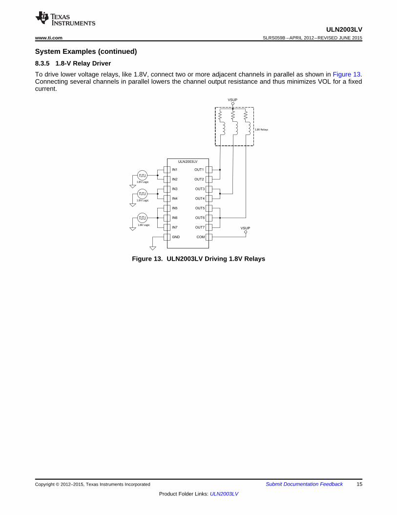
System Examples (continued)8.3.5 1.8-V Relay DriverTo drive lower voltage relays, like 1.8V, connect two or more adjacent channels in parallel as shown in Figure 13.Connecting several channels in parallel lowers the channel output resistance and thus minimizes VOL for a fixedcurrent.
Figure 13. ULN2003LV Driving 1.8V Relays
Copyright © 2012–2015, Texas Instruments Incorporated Submit Documentation Feedback 15
Product Folder Links: ULN2003LV

N
D OLi Li
i 1
P V I
=
= ´å
1
2
3
4
5
6
7
8 9
10
11
12
13
14
15
16
Cbypass 0.1uF
IN1 OUT1
IN2 OUT2
IN3 OUT3
IN4 OUT4
IN5 OUT5
IN6 OUT6
IN7 OUT7
Gnd COM
ULN2003LVSLRS059B –APRIL 2012–REVISED JUNE 2015 www.ti.com
9 Power Supply RecommendationsThe COM pin is the power supply pin of this device to power the gate drive circuitry. Although not required butdepending on the power supply, TI recommends to put a bypass capacitor of 100 nF across the Vcom pin andGnd.
10 Layout
10.1 Layout GuidelinesThin traces can be used on the input due to the low current logic that is typically used to drive ULN2003LV. Takecare to separate the input channels as much as possible, as to eliminate cross-talk. Thick traces arerecommended for the output, in order to drive high currents that may be needed. Wire thickness can bedetermined by the trace material's current density and desired drive current. Since all of the channels currentsreturn to a common ground, it is best to size that trace width to be very wide. Some applications require up to 1A.
10.2 Layout Example
Figure 14. Layout Example Recommendation
10.3 On-Chip Power DissipationUse Equation 3 to calculate ULN2003LV on-chip power dissipation PD:
where• N is the number of channels active together.• VOLi is the OUTi pin voltage for the load current ILi. (3)
16 Submit Documentation Feedback Copyright © 2012–2015, Texas Instruments Incorporated
Product Folder Links: ULN2003LV
( )J(MAX) A
(MAX)JA
T TPD
-=
q
ULN2003LVwww.ti.com SLRS059B –APRIL 2012–REVISED JUNE 2015
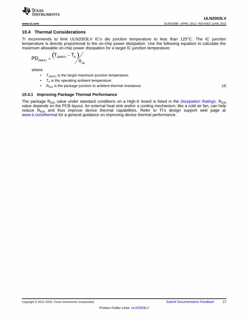
10.4 Thermal ConsiderationsTI recommends to limit ULN2003LV IC’s die junction temperature to less than 125°C. The IC junctiontemperature is directly proportional to the on-chip power dissipation. Use the following equation to calculate themaximum allowable on-chip power dissipation for a target IC junction temperature:
where• TJ(MAX) is the target maximum junction temperature.• TA is the operating ambient temperature.• RθJA is the package junction to ambient thermal resistance. (4)
10.4.1 Improving Package Thermal PerformanceThe package RθJA value under standard conditions on a High-K board is listed in the Dissipation Ratings. RθJAvalue depends on the PCB layout. An external heat sink and/or a cooling mechanism, like a cold air fan, can helpreduce RθJA and thus improve device thermal capabilities. Refer to TI’s design support web page atwww.ti.com/thermal for a general guidance on improving device thermal performance.
Copyright © 2012–2015, Texas Instruments Incorporated Submit Documentation Feedback 17
Product Folder Links: ULN2003LV
ULN2003LVSLRS059B –APRIL 2012–REVISED JUNE 2015 www.ti.com
11 Device and Documentation Support
11.1 Community ResourcesThe following links connect to TI community resources. Linked contents are provided "AS IS" by the respectivecontributors. They do not constitute TI specifications and do not necessarily reflect TI's views; see TI's Terms ofUse.
TI E2E™ Online Community TI's Engineer-to-Engineer (E2E) Community. Created to foster collaborationamong engineers. At e2e.ti.com, you can ask questions, share knowledge, explore ideas and helpsolve problems with fellow engineers.
Design Support TI's Design Support Quickly find helpful E2E forums along with design support tools andcontact information for technical support.
11.2 TrademarksE2E is a trademark of Texas Instruments.All other trademarks are the property of their respective owners.
11.3 Electrostatic Discharge CautionThese devices have limited built-in ESD protection. The leads should be shorted together or the device placed in conductive foamduring storage or handling to prevent electrostatic damage to the MOS gates.
11.4 GlossarySLYZ022 — TI Glossary.
This glossary lists and explains terms, acronyms, and definitions.
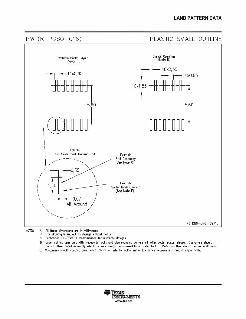
12 Mechanical, Packaging, and Orderable InformationThe following pages include mechanical, packaging, and orderable information. This information is the mostcurrent data available for the designated devices. This data is subject to change without notice and revision ofthis document. For browser-based versions of this data sheet, refer to the left-hand navigation.
18 Submit Documentation Feedback Copyright © 2012–2015, Texas Instruments Incorporated
Product Folder Links: ULN2003LV
PACKAGE OPTION ADDENDUM
www.ti.com 19-Jun-2015
Addendum-Page 1
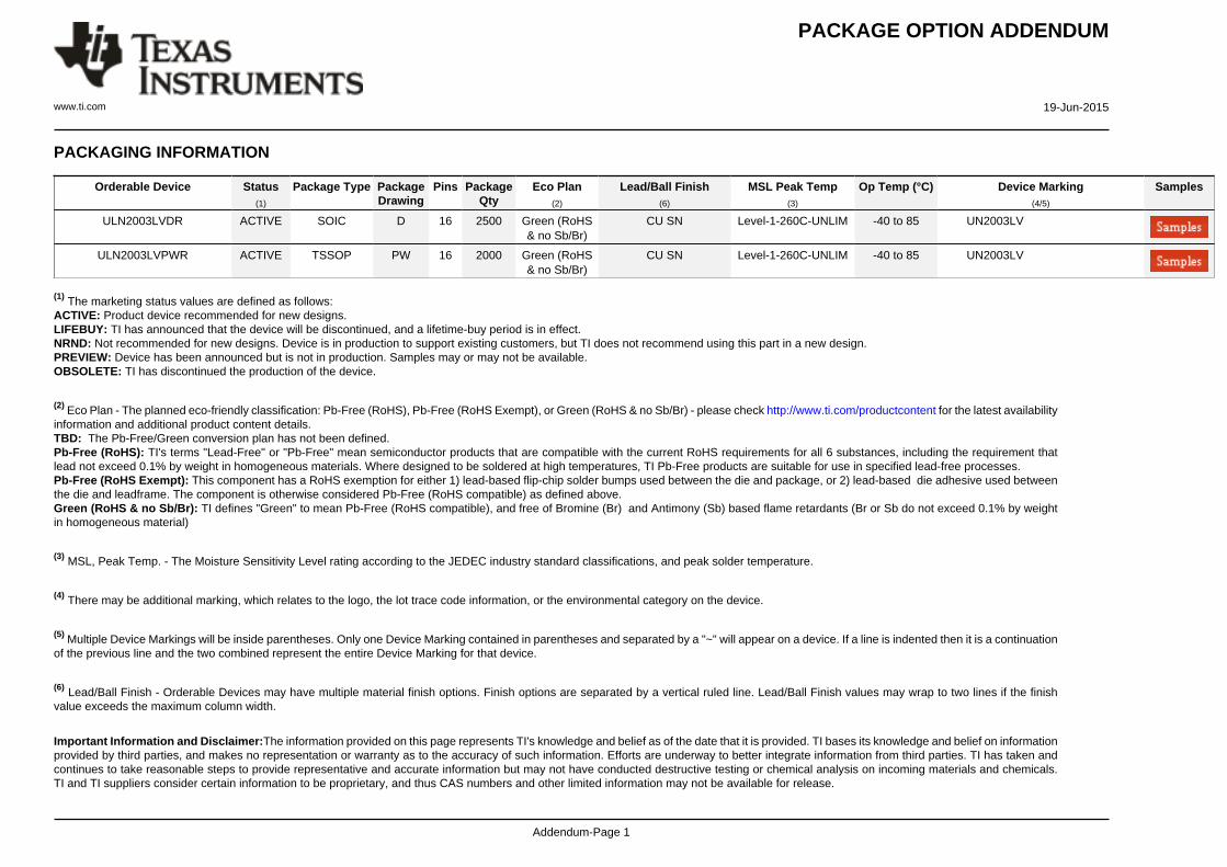
PACKAGING INFORMATION
Orderable Device Status(1)
Package Type PackageDrawing
Pins PackageQty
Eco Plan(2)
Lead/Ball Finish(6)
MSL Peak Temp(3)
Op Temp (°C) Device Marking(4/5)
Samples
ULN2003LVDR ACTIVE SOIC D 16 2500 Green (RoHS& no Sb/Br)
CU SN Level-1-260C-UNLIM -40 to 85 UN2003LV
ULN2003LVPWR ACTIVE TSSOP PW 16 2000 Green (RoHS& no Sb/Br)
CU SN Level-1-260C-UNLIM -40 to 85 UN2003LV
(1) The marketing status values are defined as follows:ACTIVE: Product device recommended for new designs.LIFEBUY: TI has announced that the device will be discontinued, and a lifetime-buy period is in effect.NRND: Not recommended for new designs. Device is in production to support existing customers, but TI does not recommend using this part in a new design.PREVIEW: Device has been announced but is not in production. Samples may or may not be available.OBSOLETE: TI has discontinued the production of the device.
(2) Eco Plan - The planned eco-friendly classification: Pb-Free (RoHS), Pb-Free (RoHS Exempt), or Green (RoHS & no Sb/Br) - please check http://www.ti.com/productcontent for the latest availabilityinformation and additional product content details.TBD: The Pb-Free/Green conversion plan has not been defined.Pb-Free (RoHS): TI's terms "Lead-Free" or "Pb-Free" mean semiconductor products that are compatible with the current RoHS requirements for all 6 substances, including the requirement thatlead not exceed 0.1% by weight in homogeneous materials. Where designed to be soldered at high temperatures, TI Pb-Free products are suitable for use in specified lead-free processes.Pb-Free (RoHS Exempt): This component has a RoHS exemption for either 1) lead-based flip-chip solder bumps used between the die and package, or 2) lead-based die adhesive used betweenthe die and leadframe. The component is otherwise considered Pb-Free (RoHS compatible) as defined above.Green (RoHS & no Sb/Br): TI defines "Green" to mean Pb-Free (RoHS compatible), and free of Bromine (Br) and Antimony (Sb) based flame retardants (Br or Sb do not exceed 0.1% by weightin homogeneous material)
(3) MSL, Peak Temp. - The Moisture Sensitivity Level rating according to the JEDEC industry standard classifications, and peak solder temperature.
(4) There may be additional marking, which relates to the logo, the lot trace code information, or the environmental category on the device.
(5) Multiple Device Markings will be inside parentheses. Only one Device Marking contained in parentheses and separated by a "~" will appear on a device. If a line is indented then it is a continuationof the previous line and the two combined represent the entire Device Marking for that device.
(6) Lead/Ball Finish - Orderable Devices may have multiple material finish options. Finish options are separated by a vertical ruled line. Lead/Ball Finish values may wrap to two lines if the finishvalue exceeds the maximum column width.
Important Information and Disclaimer:The information provided on this page represents TI's knowledge and belief as of the date that it is provided. TI bases its knowledge and belief on informationprovided by third parties, and makes no representation or warranty as to the accuracy of such information. Efforts are underway to better integrate information from third parties. TI has taken andcontinues to take reasonable steps to provide representative and accurate information but may not have conducted destructive testing or chemical analysis on incoming materials and chemicals.TI and TI suppliers consider certain information to be proprietary, and thus CAS numbers and other limited information may not be available for release.
PACKAGE OPTION ADDENDUM
www.ti.com 19-Jun-2015
Addendum-Page 2
In no event shall TI's liability arising out of such information exceed the total purchase price of the TI part(s) at issue in this document sold by TI to Customer on an annual basis.

TAPE AND REEL INFORMATION
*All dimensions are nominal
Device PackageType
PackageDrawing
Pins SPQ ReelDiameter
(mm)
ReelWidth
W1 (mm)
A0(mm)
B0(mm)
K0(mm)
P1(mm)
W(mm)
Pin1Quadrant
ULN2003LVDR SOIC D 16 2500 330.0 16.8 6.5 10.3 2.1 8.0 16.0 Q1
ULN2003LVPWR TSSOP PW 16 2000 330.0 12.4 6.9 5.6 1.6 8.0 12.0 Q1
PACKAGE MATERIALS INFORMATION
www.ti.com 19-Jun-2015
Pack Materials-Page 1
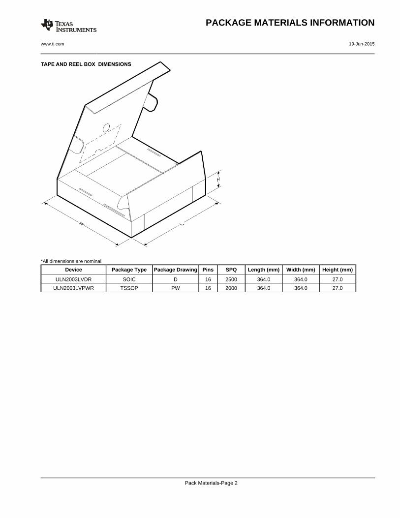
*All dimensions are nominal
Device Package Type Package Drawing Pins SPQ Length (mm) Width (mm) Height (mm)
ULN2003LVDR SOIC D 16 2500 364.0 364.0 27.0
ULN2003LVPWR TSSOP PW 16 2000 364.0 364.0 27.0
PACKAGE MATERIALS INFORMATION
www.ti.com 19-Jun-2015
Pack Materials-Page 2


IMPORTANT NOTICE
Texas Instruments Incorporated and its subsidiaries (TI) reserve the right to make corrections, enhancements, improvements and otherchanges to its semiconductor products and services per JESD46, latest issue, and to discontinue any product or service per JESD48, latestissue. Buyers should obtain the latest relevant information before placing orders and should verify that such information is current andcomplete. All semiconductor products (also referred to herein as “components”) are sold subject to TI’s terms and conditions of salesupplied at the time of order acknowledgment.TI warrants performance of its components to the specifications applicable at the time of sale, in accordance with the warranty in TI’s termsand conditions of sale of semiconductor products. Testing and other quality control techniques are used to the extent TI deems necessaryto support this warranty. Except where mandated by applicable law, testing of all parameters of each component is not necessarilyperformed.TI assumes no liability for applications assistance or the design of Buyers’ products. Buyers are responsible for their products andapplications using TI components. To minimize the risks associated with Buyers’ products and applications, Buyers should provideadequate design and operating safeguards.TI does not warrant or represent that any license, either express or implied, is granted under any patent right, copyright, mask work right, orother intellectual property right relating to any combination, machine, or process in which TI components or services are used. Informationpublished by TI regarding third-party products or services does not constitute a license to use such products or services or a warranty orendorsement thereof. Use of such information may require a license from a third party under the patents or other intellectual property of thethird party, or a license from TI under the patents or other intellectual property of TI.Reproduction of significant portions of TI information in TI data books or data sheets is permissible only if reproduction is without alterationand is accompanied by all associated warranties, conditions, limitations, and notices. TI is not responsible or liable for such altereddocumentation. Information of third parties may be subject to additional restrictions.Resale of TI components or services with statements different from or beyond the parameters stated by TI for that component or servicevoids all express and any implied warranties for the associated TI component or service and is an unfair and deceptive business practice.TI is not responsible or liable for any such statements.Buyer acknowledges and agrees that it is solely responsible for compliance with all legal, regulatory and safety-related requirementsconcerning its products, and any use of TI components in its applications, notwithstanding any applications-related information or supportthat may be provided by TI. Buyer represents and agrees that it has all the necessary expertise to create and implement safeguards whichanticipate dangerous consequences of failures, monitor failures and their consequences, lessen the likelihood of failures that might causeharm and take appropriate remedial actions. Buyer will fully indemnify TI and its representatives against any damages arising out of the useof any TI components in safety-critical applications.In some cases, TI components may be promoted specifically to facilitate safety-related applications. With such components, TI’s goal is tohelp enable customers to design and create their own end-product solutions that meet applicable functional safety standards andrequirements. Nonetheless, such components are subject to these terms.No TI components are authorized for use in FDA Class III (or similar life-critical medical equipment) unless authorized officers of the partieshave executed a special agreement specifically governing such use.Only those TI components which TI has specifically designated as military grade or “enhanced plastic” are designed and intended for use inmilitary/aerospace applications or environments. Buyer acknowledges and agrees that any military or aerospace use of TI componentswhich have not been so designated is solely at the Buyer's risk, and that Buyer is solely responsible for compliance with all legal andregulatory requirements in connection with such use.TI has specifically designated certain components as meeting ISO/TS16949 requirements, mainly for automotive use. In any case of use ofnon-designated products, TI will not be responsible for any failure to meet ISO/TS16949.
Products ApplicationsAudio www.ti.com/audio Automotive and Transportation www.ti.com/automotiveAmplifiers amplifier.ti.com Communications and Telecom www.ti.com/communicationsData Converters dataconverter.ti.com Computers and Peripherals www.ti.com/computersDLP® Products www.dlp.com Consumer Electronics www.ti.com/consumer-appsDSP dsp.ti.com Energy and Lighting www.ti.com/energyClocks and Timers www.ti.com/clocks Industrial www.ti.com/industrialInterface interface.ti.com Medical www.ti.com/medicalLogic logic.ti.com Security www.ti.com/securityPower Mgmt power.ti.com Space, Avionics and Defense www.ti.com/space-avionics-defenseMicrocontrollers microcontroller.ti.com Video and Imaging www.ti.com/videoRFID www.ti-rfid.comOMAP Applications Processors www.ti.com/omap TI E2E Community e2e.ti.comWireless Connectivity www.ti.com/wirelessconnectivity
Mailing Address: Texas Instruments, Post Office Box 655303, Dallas, Texas 75265Copyright © 2016, Texas Instruments Incorporated
Related Documents