156 APPENDIX B: EUROPEAN SITE REPORTS Site: DaimlerChrysler Ulm, GERMANY Date Visited: 9 June 1999 TTEC Attendees: J. Zavada (report author) Hosts: Prof. Hermann Schumacher, University of Ulm Dr. Andrei Vescan, DaimlerChrysler Dr. Helmut Leier, DaimlerChrysler DAIMLERCHRYSLER Introduction DaimlerChrysler is a German-American company that was formed by the merger of two industrial giants, Daimler-Benz and Chrysler, in 1997. On Wednesday afternoon, Dr. Zavada met with Dr. Helmut Leier, who is director of the high frequency electronics department, and with Dr. Andrei Vescan, who is involved with research technology of III-V components. Dr. Leier gave an overview of DaimlerChrysler and its research activities. The central research center employs about 1,800 people and sponsors nearly 500 students. Since the main activity of the company is automobiles, much of the research activities concentrate on cars and traffic. There are three main areas of research: microelectronics and micro-systems; information and communications; and high frequency devices. Currently, most of the high frequency device work is based on GaAs. High power (> 1 W/mm), high frequency (> 10 GHz) HEMTs and MESFETs are being developed. The research on GaN is directed at extending the performance of the GaAs devices. Dr. Leier emphasized the importance of minimizing the cost while extending device performance. High power GaN devices will not make a major impact until fabrication costs are competitive with GaAs devices. Dr. Leier also mentioned that DaimlerChrysler is part owner, with Thomson-CSF, in United Monolithic Semiconductor (UMS). DaimlerChrysler acquires the GaAs wafers for high power devices from UMS. III-V Components Dr. Vescan gave Dr. Zavada a presentation on the research at DaimlerChrysler concerning high frequency, high power GaN-based devices. He said that DaimlerChrysler is not presently involved with growth of GaN films. SVT Associates, in the United States, is collaborating with DaimlerChrysler and currently provides the necessary films. The work at DaimlerChrysler centers on the design, processing, and fabrication of GaN- based devices. Dr. Vescan said that the optimum processing conditions are very dependent upon the source of the GaN films. These conditions can be determined only after repeated trials and device testing. The group at DaimlerChrysler has been working in close collaboration with Prof. Kohn at the University of Ulm on device properties of AlGaN/GaN MODFETs (modulation doped field effect transistors). Clean Room Facilities Later in the afternoon, Dr. Leier and Dr. Vescan took Dr. Zavada on a tour of the clean room facilities at DaimlerChrysler. The clean rooms are similar to the ones at the University of Ulm; however, they are larger, measuring approximately 1,000 sq. meters. Some areas are class 100 and others are class 10. Following the merger of Daimler-Benz and Chrysler, half of the clean space was divided between DaimlerChrysler and UMS. I was only shown the DaimlerChrysler clean rooms. Still they comprise a first-rate facility for processing III-V materials.

Welcome message from author
This document is posted to help you gain knowledge. Please leave a comment to let me know what you think about it! Share it to your friends and learn new things together.
Transcript
156
APPENDIX B: EUROPEAN SITE REPORTS
Site: DaimlerChryslerUlm, GERMANY
Date Visited: 9 June 1999
TTEC Attendees: J. Zavada (report author)
Hosts: Prof. Hermann Schumacher, University of UlmDr. Andrei Vescan, DaimlerChryslerDr. Helmut Leier, DaimlerChrysler
DAIMLERCHRYSLER
Introduction
DaimlerChrysler is a German-American company that was formed by the merger of two industrial giants,Daimler-Benz and Chrysler, in 1997. On Wednesday afternoon, Dr. Zavada met with Dr. Helmut Leier, whois director of the high frequency electronics department, and with Dr. Andrei Vescan, who is involved withresearch technology of III-V components.
Dr. Leier gave an overview of DaimlerChrysler and its research activities. The central research centeremploys about 1,800 people and sponsors nearly 500 students. Since the main activity of the company isautomobiles, much of the research activities concentrate on cars and traffic.
There are three main areas of research: microelectronics and micro-systems; information andcommunications; and high frequency devices. Currently, most of the high frequency device work is based onGaAs. High power (> 1 W/mm), high frequency (> 10 GHz) HEMTs and MESFETs are being developed.The research on GaN is directed at extending the performance of the GaAs devices. Dr. Leier emphasizedthe importance of minimizing the cost while extending device performance. High power GaN devices willnot make a major impact until fabrication costs are competitive with GaAs devices. Dr. Leier also mentionedthat DaimlerChrysler is part owner, with Thomson-CSF, in United Monolithic Semiconductor (UMS).DaimlerChrysler acquires the GaAs wafers for high power devices from UMS.
III-V Components
Dr. Vescan gave Dr. Zavada a presentation on the research at DaimlerChrysler concerning high frequency,high power GaN-based devices. He said that DaimlerChrysler is not presently involved with growth of GaNfilms. SVT Associates, in the United States, is collaborating with DaimlerChrysler and currently providesthe necessary films. The work at DaimlerChrysler centers on the design, processing, and fabrication of GaN-based devices. Dr. Vescan said that the optimum processing conditions are very dependent upon the sourceof the GaN films. These conditions can be determined only after repeated trials and device testing. Thegroup at DaimlerChrysler has been working in close collaboration with Prof. Kohn at the University of Ulmon device properties of AlGaN/GaN MODFETs (modulation doped field effect transistors).
Clean Room Facilities
Later in the afternoon, Dr. Leier and Dr. Vescan took Dr. Zavada on a tour of the clean room facilities atDaimlerChrysler. The clean rooms are similar to the ones at the University of Ulm; however, they are larger,measuring approximately 1,000 sq. meters. Some areas are class 100 and others are class 10. Following themerger of Daimler-Benz and Chrysler, half of the clean space was divided between DaimlerChrysler andUMS. I was only shown the DaimlerChrysler clean rooms. Still they comprise a first-rate facility forprocessing III-V materials.
HTE European Site Reports - DRAFT 157
Site: High Pressure Research Center (Workshop)Polish Academy of SciencesUl. Sokolowska 29/3701-142 Warsaw POLAND+48-226-32-5010www.unipress.waw.pl
Date Visited: 10 June 1999
TTEC Attendees: S. DenBaars (report author), M. Shur, U. Varshney, G. White
Hosts: Dr. W. Porowski (HPRC)Dr. I. Grzegory (HPRC)L. Leszynski (HPRC)L. Dobrzauski (IEMT)W. Wolosinski (Warsaw Univ. of Tech.)A. Jelenski (IEMT)J. Szmidt (Warsaw Univ. of Tech)Dr. J. Weyher (HPRC)R. Beck (Warsaw Univ. of Tech.)
BACKGROUND
A comprehensive workshop on GaN activities in Poland was held for the panel members at the High PressureResearch Center (HPRC) in Warsaw, Poland. This included groups from Warsaw University of Technology,the HPRC research group Unipress, and the Institute of Technology of Materials and Electronics (IEMT).
TECHNOLOGY DISCUSSION
Dr. Porowski of Unipress hosted the meeting at the High Pressure Research Center and had also invitedrepresentatives of several of the other leading Polish research efforts in wide bandgap semiconductors to theworkshop. Within Poland there are 14 research efforts developing GaN materials and devices. Recently thePolish government has approved funding of the large national project “Development of BlueOptoelectronics”. This program will focus on blue lasers, solar blind detectors, and full-color industrialdisplays.
GaN Bulk Substrate
Unipress is the research group within HPRC working on GaN bulk crystal growth from a melt. One of themost impressive achievements the panel saw in Europe was the “defect free” bulk GaN wafers grown frommelt under extremely high pressure. Dr. Isabel Grzegory gave an overview of the high pressure solutiongrowth method used for depositing the bulk single crystals.
The size of the substrates has steadily increased up to 1 cm in 1999 from 5 mm in 1997. In comparison toGaN on sapphire technology which exhibits 1 E+9 cm-2 defect densities, or ELO films, which are in the1 E+6 cm-2 to 5 E+5 cm-2 range, the bulk GaN crystals possess 10 to 1 defect per square centimeter. Thesedensities were estimated from etch pit counts and correlated to TEM measurements of higher defect densitiesfound on standard GaN sapphire technology.
The team was allowed to observe the bulk crystals under both optical microscopes and field emission SEM.Both n-type bulk crystals and semi-insulating bulk crystal have been grown. The semi-insulating substrateswere highly resistive 1 E+5 ohm-cm and could be used for thin film deposition of high power AlGaN/GaNmicrowave amplifiers (Litwin-Staszewska et al. 1999). Very high quality homeoepitaxial growth of GaN byMOCVD was obtained on top of these substrates and the films exhibited narrow double-crystal x-raydiffraction (DCXRD) linewidths as low as 21 arcsec. The group at University of Ulm, in collaboration with
HTE European Site Reports - DRAFT158
Unipress, has obtained thin films that exhibit the narrowest reported PL linewidths at low temperature(0.1 meV)—which is indicative of the uniform high quality film (Komitzer et al. 1999). MBE has also beenperformed on the bulk crystals. Both Ga-face and N-face polarity bulk substrates have been produced. Thebulk crystals also display extremely smooth cleaved facets with rms roughness of 5 angstroms, which wouldmake excellent laser facets.
Unipress is also investigating high power HEMTs, Schottky diodes, and UV detectros. Using MOCVDAlGaN/GaN materials have been grown with sheet carrier charge of 1.2 e+12 cm-2. Large geometry,1 micron gate length FETs have been fabricated and FET characteristics obtained. High quality Schottkycontacts were obtained using Pd/Au metallization, which exhibited barrier heights of 0.8 eV.
IEMT
Researchers at the Institute of Technology of Materials and Electronics are focusing on device fabricationand bulk growth of novel substrates. Panelists toured the facilities for fabricating laser diodes and detectors.Dr. Dobrzauski has already fabricated a GaN UV detector, which showed a peak responsivity at 364 nm.Numerous bulk crystal pullers were in operation. Also, a wide range of high quality optical bulk substrateswas being grown such as: Si, GaAs, InP, ZnSe, YAG, LiGaO2, and LiAlO2. Large banks of UPS backup areneeded to ensure safe operation in event of a power failure.
REFERENCES
Litwin-Staszewska, E., T. Suski, I. Grzegory, S. Porowski, J. Robert, D. Wasik, A. Witowski, D. Cote, and B. Clerjund. 1999. Electrical Properties of GaN Bulk Single Crsytals Doped with Mg. Paper We-P082, Proceedings of Intl.
Conf. on Nitride Semiconductors, Montpellier, France,. pg 124.
Kornitzer, K., T. Ebner, M. Grehl, K. Thonke, R. Sauer, C. Kirchner, V. Schwelger, M. Kamp, M. Leszczynski, I. Grzergory, S. Porowski. 1999. High Resolution PL and Reflectance Spectra of Homoepitaxial GaN Layers. Paper
Tu-17, Proceedings of Intl. Conf. on Nitride Semiconductors, Montpellier, France. pg. 49
HTE European Site Reports - DRAFT 159
Site: IMC, ABB, and KTHElectrum BuildingKistagangen 15Kista, Stockholm, SWEDEN
Date Visited: 11 June 1999
TTEC Attendees: T.P. Chow (report author), V. Dmitriev, M. Spencer, S. DenBaars, M. Shur,U. Varshney, G. White
Hosts (IMC): Dr. Christopher Harris, SiC Project ManagerDr. Meitek BakowskiDr. Andrey Konstantinov
Hosts (ABB): Dr. Heinz Lendenmann, Project Leader, Switch Development, SiC Project
Hosts (KTH): Dr. Mikael OostlingDr. Nils Nordell
IMC
IMC is an applied research company that facilitates technology transfer from the research and developmentstage to prototyping and manufacturing. It has received both industrial (80%) and government (20%) supportto enhance Swedish competitiveness. Recently, it has merged with IOF to form a new company calledACLEO.
IMC has mostly performed research in microelectronics and IOF on optoelectronics. The new company hasa wide range of interests in both of these technical areas and has more European presence. IMC has locationsin Kista and Linkoping. The Linkoping location focuses on interconnect and packaging of electronics andoptoelectronics systems.
There are 53 employees in Kista and 27 in Linkoping. The budget for 1998 was 85 million SEK($10.5 million) and 120 million SEK ($15 million) for Kista and Linkoping, respectively. It spins off onenew company per year on the average. There is a high labor turnover rate (15-20% per year) with theaverage age of its employees being 34.
Dr. Harris indicated that the researchers in the Kista facility perform work in a variety of areas, including (a)radiation detectors (QWIP, bolometers), (b) optoelectronics, (c) SiC electronics, particularly power devicesand (d) microsystem technology (microstructures, sensors). The wide bandgap semiconductor technologyhas mostly focused on SiC and the application areas are:
• power devices (development for ABB)
• microwave electronics (Ericsson)—high power amplifiers for base stations, 3 GHz, 100 W, entirely SiCso far, but expecting GaN to be applicable at higher frequencies
• high temperature electronics
• sensors, e.g., SiC as X-ray detectors, sensitivity close to human tissues
The highlights of specific technical activities are:
• numerical simulations and design—TMA software based
• portfolio of SiC specific process technologies
− epi growth (Emcore and Epigress reactors, process support for Epigress)
− ion implantation
− dry etching (ECR etching)
HTE European Site Reports - DRAFT160
− dielectric growth and deposition
• device and characterization
− IV, CV, DLTS, Hall
− optical
− SEM/TEM/SPM
One example of the application of these process technologies in device fabrication is the demonstration of a16 GHz (fmax) 4 H-SiC implanted-channel SiC MESFET. The gate width is 0.8 µm with optical lithographyand 2x smaller with e-beam lithography. A channel mobility of 200 cm2/V-s has been achieved. Also,measurements of basic material properties of SiC are also performed as part of the Swedish National SiCProgram (SiCEP).
Dr. Bakowski presented the high temperature electronics work. This area can be broadly categorized intotwo sub-areas:
• 200-300°C
− integrated motor control
− smart fuel pumps
− brake by wire
• 400-800(C
− combustion
− geothermal
The multi-chip module (MCM) concepts that are devised for these two temperature ranges are different.
• 200-300°C
− power electronics SiC
− sensor SiC
− control electronics Si SOI
• 400-800°C
− power electronics, sensors, control electronics, all SiC
Besides active devices, high temperature passive components also need to be addressed.
Dr. Konstantinov presented the high temperature sensor research. One approach is to use high temperaturegas-absorbing metal-gate MOSFET. Using a Pd gate, hydrocarbons (CHx) decompose after adsorption to thePd and the resulting H+ ions diffuse to the interface, thereby shifting the barrier height. The advantages ofusing SiC are:
• high operating temperature (e.g., engine exhaust at 600°C)
• fast operation
Other devices that can also be used are MOS capacitors, metal-semiconductor diodes (I-V shift) andMESFETs.
For automotive applications, compared to the conventional Lambda sensor which utilizes a thick Zr layer, thegas-sensor SiC MOSFET developed at IMC offers much faster feedback so that adjustment to each enginecylinder can be made. The salient features of this SiC MOSFET are:
• buried channel
• low threshold voltage
• high temperature operation (17 hrs at 600°C so far)
• high gas response
HTE European Site Reports - DRAFT 161
The goals of this program are:
• long term stability at 600°C
• sensitivity to exhaust products other than hydrocarbons
• electronic noses (MOSFET sensor arrays)
Different metal gates may be used to sense different gas products.
The panel was given a facility tour of the clean room area that is on the ground floor and where all themicroelectronics device processing facilities of the three institutions are housed, though separately. TheABB facility includes a high-energy (3 MeV) ion implanter that has a heated end station and a laser directwrite aligner. IMC processes a large variety of compound semiconductors for several applications (such assolar cells and optoelectronics). These facilities are very impressive and world-class.
ABB
ABB is a large international industrial company that has a major presence in power generation, transmissionand distribution. It was instrumental in getting the SiC program started in Sweden in 1988 and has sponsoredmany programs in developing the SiC infrastructure in Sweden.
Dr. Lendenmann presented an overview of the ABB businesses and elements of the SiC device program.The power generation plants include hydro, “clean coal,” nuclear power and fuel gas cleaning types. ABB isvery focused in getting SiC devices into power electronics systems. For example, for a 1-5 MW industrialconverter system, it is estimated that Si device replacement with SiC can reduce the size by 1/3. Significantimprovement in HVDC system is also projected with SiC devices, with the goal of 50 MW plant in 300 m2
area.
A 3.5 kV, 200 A 4 H-SiC pin junction rectifier was presented. The diode structure consists of a deep boronjunction for good junction leakage and a shallow aluminum implant topped with a p+ epi regrown region foroptimal contact resistivity. A multiple-zone boron-implanted JTE has been used for junction termination, inconjunction with a SiN/polyimide over the field oxide as the passivation layer. A phosphorus-implanted n+region was used as channel stop. Sensitivity analysis between device on-state voltage (VF < 4 V) vs. epithickness has been shown for correlation. The leakage current density for diodes with three different areaswas shown, with the largest device (7 x 7 mm2) size having a value of less than 10-5 A/cm2, the best value todate for large-area devices. Dynamic switching of 150 A to 800 V with a dI/dt > 200 V/µsec results in anIRP < 0.2 IF. The goal is to first implement SiC diodes with Si IGBT, with the implementation of SiC three-terminal switching devices later. Actually, they project that at higher frequencies, the Si IGBT will bethermally limited. At present, there is no GaN work at ABB.
In summary, ABB focuses on the system application and leverage of SiC devices and is perhaps mostadvanced in the world in incorporating SiC devices into power electronics systems.
ROYAL INSTITUTE OF TECHNOLGY (KTH – KUNGL TEKNISKA HOGSKOLAN)
Prof. Oostling presented his work on semiconductor devices, including heterojunction SiC HBT with GaNemitter. Prof. Oostling collaborates with many researchers around the world. The SiC/GaN HBT consists of1018 cm-3 SiC p-base, over which a n+ GaN emitter was grown by MBE. The p-base thickness can be eitheroptimized for high-voltage power (1 µm) or microwave power (optimized for 2 GHz). The device work islargely supported by SiC EP program of the Swedish government. The heterojunction GaN/SiC diode hasbeen improving, reaching a low value of IR ~ 10-4 A/cm2 at –50V, which is close to ideal. SiC MISFET withMBE grown 17 nm AlN has also been fabricated. The device is functional but the gate is still leaky. Prof.Oostling is well known for his contact work on SiC. TiC formation with CoSi2/Ti bilayer after 900°C annealleads to a low contact resistivity (10-6 Ω-cm2) on p-type, 1019 cm-3 doped epi of 6H-SiC. He is also exploringepi TiC layer on SiC that can be formed at 500°C or lower.

HTE European Site Reports - DRAFT162
Dr. Nordell presented the clean room organization, funding structure and the various programs that utilize thefacilities.
Addendum: High Temperature Packaging Capability (George White)
Dr. Chris Harris indicated to us that most of the packaging efforts for IMC were being conducted inLinkoping. However, the effort there is focused primarily on Si multi-chip modules. There they havedemonstrated a 3" x 2" compact computing module which consists of a processor and memory chips.
Dr. Vladimir Dmitriev introduced us to Dr. Roumen Kakanakov of the Institute of Applied Physics ofPlovdiv, Bulgaria. Dr. Kakanakov, who by chance was working at the offices of IMC during our visit, is aleading authority on high temperature packaging. He has started a small company, called "________" whichis doing R&D in microelectronics, optoelectronics and sensor semiconductor devices, on Si, GaAs and SiCsubstrates. Their expertise is in the field of ohmic contacts and packaging. Unfortunately, we were unableto meet with Dr. Kakanakov for any useful length of time, but we subsequently communicated with him viatelephone and e-mail. Below is a summary of the conversation and correspondence with Dr. Kakanakov.
In our evaluation of high temperature electronics in Europe, there were very few programs associated withpackaging of components for temperatures above 300°C. Therefore, Dr. Kakanakov was asked to commenton a number of questions. Below is a summary of his responses.
Q: What plans are in place to package SiC and GaN devices at temperatures above 300°C ?
A: The problems of high temperature electronics packaging were addressed through European project CP94063 "Contacts encapsulants and packaging for high temperatures silicon carbide microelectronics", whereKakanakov et al. were responsible for:
• development and manufacture of high temperature packages for power SiC MESFET'S (300-350oC)• R&D work on packaging processes for SiC chips, which involved the choice of SiC back side
metallization, high temperature attach material and chip attachment process to the package—all of whichcontribute to device reliability at high temperatures (300-350oC)
• evaluation of the reliability of the SiC MESFETs and the packaging process during a 350°C storage test• measurement of thermal resistance (Rth)and its behavior during the storage test
After completion of this project in 1997, Kakanakov continued to make a small series of packages for powerSiC MESFETs from Thomson-CSF. In early 1999, work began on the NATO project "High Power and HighFrequency Devices on LPE-Grown SiC Films", where the packaging group was responsible for R&D ofpackages and packaging of power SiC diodes. It was also indicated that Kakanakov may have the possibilityto get involved in packaging of GaN/SiC HBTs for this project.
An important element in the packaging of high temperature electronics is the base substrate material andattach material. Kakanakov was asked to comment on his work in this area.
As a material for the package base plate, Kakanakov chose a Mo-Cu alloy because of its high electrical andthermo conductivity, and good mechanical properties at high temperatures. Two gold based alloy materialswere used as attach materials. The attach materials were gold based alloys of Au (6%) and Si, and Au (12%).The 6% alloy has a melting point of 373oC, and the 12% alloy melts at 363oC. Eventually the groupprimarily concentrated on the first alloy as the attach material. The backside contact metallization that wasused was Ti-Pt-Au on SiC. The advantage here was no change in thermal resistance during high temperaturetesting. However, Pt and Ti will dissolve in the Au/Si solder when it is liquidus, thereby indicating that moresuitable barrier metallurgies will have to be identified at the temperature extremes. Gold wiring bonding isperformed using a ball bonder from K&S when making connections from the chip to substrate. When askedabout the packaging of passive components, Kakanakov indicated that in principle the same attach material

HTE European Site Reports - DRAFT 163
could be used to attach the passives, but they have no experience with attaching cermet components at hightemperature.
From a reliability standpoint Kakanakov agrees that new reliability test equipment and methodologies maybe needed for high temperature reliability assessment. Limited reliability data exist for some of theirsystems; however, some reliability studies were done using thermal resistance measurements. An importantneed for the advancement of high temperature electronics packaging will be the advent of reliabilitymodeling and simulation.
HTE European Site Reports - DRAFT164
Site: Infineon Corporate Research (formerly Siemens AG)Siemens Munich Corporate Research LaboratoryOtto-Hahn-Ring 6D-81-730 Munich GERMANYTel: +49-89656-45230Fax: +49-89656-53294
Date Visited: 9 June 1999
TTEC Attendees: S. DenBaars (report author), M. Shur, U. Varshney, J. Zavada, G. White
Hosts: Dr. Henning ReichertDr. Walter KellnerDr. Eckhard WolfgangDr. Peter Turkes
BACKGROUND
The Siemens Munich Corporate Research Laboratory is the main research arm of Siemens’ semiconductorbusiness. Siemens has recently spun off Infineon Technologies which will be responsible for semiconductorcomponents. Infineon and Osram also have a joint venture to develop GaN blue LEDs and solid-state whitelighting using GaN based LEDs. Infineon has a large GaN on SiC LED fabrication facility at Regensburg,Germany. White LED products have recently been introduced by Osram under the trademarked name ofTOPLED. In Munich the Central Research Laboratory is involved in GaN MBE (lead by Dr. Reichert),while the GaN optoelectronics effort at Regensburg is primarily using MOCVD.
TECHNOLOGY DISCUSSION
Dr. W. Kellner gave a review of Infineon GaAs products and developments in electronics. As wide bandgapsemiconductors may play a role in the microwave power electronic area, Dr. Kellner informed the panel ofsome recent developments in power electronics. Cellular phone base stations, radio links, and automotiveradar are three large applications where semiconductor products are beginning to appear. The automotiveradar application requires 77 GHz and only 20 mW; therefore GaAs products are most likely to be marketedfirst. In the cellular base station application very high powers of 20 to 100 Watts are required at frequenciesabove 2 GHz. It is unclear if GaN or SiC can address this market at this stage of development, butdevelopment on both materials is progressing.
The GaN molecular beam epitaxy (MBE) effort at Siemens was reviewed in detail by Dr. Henning Reichert.Currently the MBE effort is shifting its focus away from optoelectronics and is emphasizing the highmicrowave power electronic devices. However, Dr. Reichert recently carried out very good fundamentalstudy of GaN and InGaN growth by MBE. P-type doping as high as 1 E+18 cm-3 was achieved by MBE.This is important for low contact resistance to LEDs and lasers. A high growth rate of 1.4 microns/hr wasachieved and mobilities as high as 460 cm2/V-sec by MBE growth of GaN on MOCVD GaN templates. Animpressive study of InGaN growth yielded good PL as long as 540 nm. Recently single crystal InN wasachieved at a growth temperature of 400°C. Dr. Reichert observes a thermal decomposition temperature of530°C in MBE, which is close to the value obtained by Ombacher et al in 199???. P-type GaN studiesindicate an activation energy of 150 meV. The future emphasis in the MBE lab will be on AlGaN/GaNelectronic devices and GaAsN for long wavelength lasers.
Siemens Corporate Research Laboratory also has a high temperature silicon electronics effort underway. Dr.Eckhard Wolfgang reviewed the status of silicon on insulator (SOI) and SiC technology at Siemens. SOI isthe main material being developed, with SOI technology way ahead of other materials in terms ofcommercialization. Currently SOI is used for 8 kV thyristors and IGBT 3 kV with are used in railway tram.Eighteen modules are used for power switching of megawatts in railway systems. There is a small research
HTE European Site Reports - DRAFT 165
effort on investigating the new wide bandgap semiconductors (mainly SiC) for higher temperature operation.SiC is mainly being look at for high temperature applications. Currently, silicon is limited to operationtemperatures below 200°C. Therefore SiC and GaN could play a role above 200°C. In automotiveapplications several areas have temperatures in which silicon based devices can be placed. These are incombustion, exhaust, on the engine, and mounted near the brakes. Even if wide bandgap semiconductors canoperate at these temperatures, new packaging technology is needed to make devices stand-up to these harshenvironments. In addition, reliability of 35 years before failure needs to be designed into the parts. Dr.Wolfgang concluded by saying that much work is needed before WBS can play a role in the high temperatureautomotive markets.
Pspice models for modeling power electronic devices are available on the web at www.infineon.com.

HTE European Site Reports - DRAFT166
Site: Laboratoire d’Electronique de Technologie et d’Instrumentation (LETI)
Date Visited: 7 June 1999
TTEC Attendees: M. Shur (report author)
Hosts: Dr. Serge Valette, Head of LETI programsDr. C. Brylinski, Thomson-CSFDr. JolyDr. J. DubozDr. M. DenevilleDr. H. Bergonzo
LETI: THE LARGEST CLEAN ROOM IN EUROPE
LETI (Laboratoire d'Electronique de Technologie et d'Instrumentation) is one of France’s largest researchinstitutions. Nine hundred fifty people worked at LETI as of the end of 1998 (722 CEA personnel and 212personnel of different affiliations, including 165 industrial researchers). LETI consists of five departmentsand several programs. Fig. 1 shows the organizational structure of LETI.
Director
Departments Prog
ElectronicsSy
Fig. 1. LETI organizational structure.
LETI strongly emphasizes technology transfer. Feedback loops exist between LETI and French andEuropean industry; LETI possesses hundreds of patents and encouraged spin-offs.
The largest efforts (by percent of total personnel involved) are in microelectronics (27%), defense (22%),nuclear electronics (13%), medical/biological electronics applications (8%), professional electronics (7%),information technology—hardware and software (7%), computer peripherals (6%), telecommunications(5%), and aerospace (5%).
Dr. Serge Valette, Head of LETI programs, described the LETI organizational chart and the major researchthrusts. The areas of research and development include
Microelectronics
• CMOS 0.12 - 0.18
• SOI
• Single electron transistor
Microtechnologies
• Sensors
HTE European Site Reports - DRAFT 167
• MEMs
• Recording and displays (fluorescent tip displays)
• Silicon microwave power
• Packages and interconnects
Optoelectronics
• Infrared photodetection (cooled and uncooled)
• Materials for optics
Microlasers
• Laser induced damage threshold from UV to infrared
• Physico-chemical characterization of materials and thin films
Systems
• Electronics for medical applications
• Medical imaging
• Biochip
• Information technology
• Nuclear instrumentation
• Sensors
• Organic components (polymers for optical applications)
• Organic LEDs and flat screens
SILICON-ON-INSULATOR
Drs. B. Aspar and J. L. Pelloie presented the results of silicon-on-insulator (SOI) research at LETI. Hedescribed the Smart Cut® process and demonstrated that the quality of Si bonded using the Smart Cut®process is similar to that of the starting material. This technology is applicable not only to Si but also toGaAs-based materials and SiC. For silicon technology, SOI technology demonstrates a higher temperatureperformance.
SIC ACTIVITIES IN FRANCE
Dr. C. Brylinski of Thomson-CSF reported on the results of SiC research in France. This is his summary ofthe status of SiC research in France:
• Crystals: research stage
• Wafers: started development
• Devices: started development
• Equipment: first demonstration
SiC epitaxy activity is primarily in LETI and in approximately 10 universities.
Funding sources include: CNRS, industry, and defense programs. SiC projects are divided into those that arepart of national programs and those that are part of European programs.
Two national programs in SiC include "Saut Technologique", which is a three-year program (funded by thegovernment and coordinated by industry, with industrial partners contributing some funding as well).
HTE European Site Reports - DRAFT168
The European SiC program has a goal of achieving 3 inch wafers with no micropipes in three??? and toobtain a low defect density on 2 inch wafers (less than 10 micropipes per cm2). Under the auspices of thisproject, the French have teamed with a Swedish-Finnish company, Okmetic.
More detailed goals include cheaper and bigger crystals, lower defect density, the development of a SiCfabrication process compatible with a silicon line, the development of MOS and HBT devices.
Thomson-CSF is developing recessed SiC MESFETs. They fabricated modules with the total 14.4 mm gateperiphery with four chips. For devices with wide gates (a few mm), the microwave power was on the orderof 1 W/mm; for narrow gate devices, it was about 4 W/mm. The devices were operational up to 500°C inCopernicus package (AlCuMo frame package). In devices fabricated on semi-insulating SiC substrates, thecurrent decreased with time and disappeared in approximately 100s. (Most likely this is a trapping program,most likely associated with vanadium.) The devices fabricated on conductive substrates did not exhibit thiseffect.
Dr. Joly described the bulk SiC material grown at LETI. The boule diameter was 50 mm. However, thematerial quality was inferior at the edges. They are using an Epigress two reactor system. The effort at LETIalso includes the simulation of crystal growth. Best results achieved at LETI include 95 mohm cm,p = 1019 cm-3, 14% activation for 1021 cm-3 of Al acceptors. A p-n junction operated at 650°C. The junctiondepth was 220 nm.
There are two European projects dealing with SiC. The funding scale is on the order of one million dollarsper year. The first project is called TECSICA. This project provided the basic research funding.
The participants are:
• T.U.B. Berlin
• UAB/CCM (Barcelona)
• Aristoyeles Univ. (Thessaloniki)
• F.O.R.T.H. (Crete)
Endorsers:
• Schlumberger (Clamart)
• C. S. GmbH (Munich)
• LETI (Grenoble)
The second project is called SICOIN. This is an industrial project. Its main goal is to develop a hightemperature pressure sensor.
The participants are
• Daimler
• Schlumberger (Clamart)
• T.U.B Berlin
• Aristoyeles Univ. (Thessaloniki)
• Epichem
GaN-RELATED RESEARCH IN FRANCE
Dr. J. Duboz gave an overview of GaN-related research in France.
• Lille: CNRS—Process, electronics
• Caen: CNRS and University—Crystallography
• Strasbourg: CNRS—Nonlinear optics
HTE European Site Reports - DRAFT 169
• Orsay: Thomson-CSF—Everything
• Clermond Ferran: University—Growth, optical
• Lyons: University—Optical
• Grenoble: CEA—Growth (MBE), optical
• Montpellier: ???—Growth (MOCVD), characterization)
• Valbonne: CNRS—Growth optical studies
• EEC project
ANISET: Material oriented. Developed a commercial reactor (available from Riber). Also ECR source andthermal cracker
LAQUANI: Material and device oriented
− Nottingham, Madrid, Lausanne, CNRS (finished), EPFL
− Valbonne (finished)
RAINBOW: Multicolor LEDs and blue laser
− Thomson-CSF
− Philips
− Axion
− Epichem
− University of Seville
− Valbonne
− Erlangen
− Surrey
− Aveires
MIGHT: Material and device oriented high power, high frequency electronics ???/ HEMT 5 W, 10 GHz, -goals;
− GEC, Thomson-CSF
− Siemens
− Thomas Swan, Univ. Nottingham, Univ. of Gent
Started this year
Total budget 3-4 million Euro per project per year
Results:
Materials
− P doping 5 x10¹⁷ (Valbonne, 3 MBE, 5 MOCVD), conductivity 1 ohm-cm
− InGaN bulk FWHM 50 meV at 10 K, 400 nm, Stokes shift < 30 meV
− InGaN QW FWHM 35 meV at 10 K
− GaN/AlGaN QW FWHM 15 meV at 10 K
ELOG-HVPE
− GaN on Si (111) quality similar to sapphire
HTE European Site Reports - DRAFT170
− GaN/AlGaN quantum dots: intense, large Stark effect (red PL)
Process:
− n-contact 10-6 ohm cm2
− p-contact 10-3 ohm cm2
− Etching: vertical facets by CAIBE and optically pumped laser
LEDs
− <-/1 mW ???
− GWHM 15 nm at 235 nm
− High turn-on voltage
Laser
− Optical pumped
FETs
MESFETs
2 micron gate, breakdown ~ 300 V, for a 0.3 micron gate, ft = 12 GHz fmax = 25 max Idss = 330 mA/mm
Photodetectors
Photoconductive
3000 A/W
UV-visible 104 to 107
1/f noise is large
Schottky photovoltaic on GaN
ns response
10-8 A reverse current
Johnson noise low bias
roA 108 W cm2
Schottky photovoltaic on AlGaN
Cutoff at 320 nm
4-year delay compared to US
Materials are catching up. Devices behind, except for photodetectors (state of the art)
DIAMOND RESEARCH IN FRANCE
Drs. M. Deneville and P. H. Bergonzo discussed diamond research in France.
Applications
− window (microwave and laser)
HTE European Site Reports - DRAFT 171
− pressure sensors and SAW
− UV,V, X, and particle detectors
Coating
− Electrochemical reactions
p-n junction 900 oC
Schottky 700 oC
MESFET 500 oC
Groups in France
Window (microwave and laser)
Thomson, CEA in Bordeaux
LPL Paris
SAW (with AlN), Univ. Lens
Pressure sensors and SAW
Univ. of Nancy
UV,V, X, and particle detectors
Coating
University of Orleans
Electrochemical reactions:
LCTMR, CNRS
Basic research
Reactor modeling
Large monocrystalline substrates
Physical and electrical properties
Device
Schottky
MESFET
Surface studies
At LETI, they have grown 0.5 cm 250 micron diamond crystal film.
HTE European Site Reports - DRAFT172
Site: Russian GaN-based ResearchVirtual Site Report
Date: 12 June 1999
Report Author: M. Shur
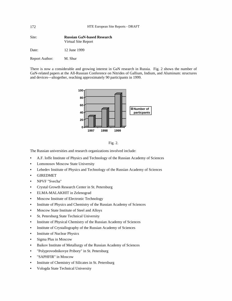
There is now a considerable and growing interest in GaN research in Russia. Fig. 2 shows the number ofGaN-related papers at the All-Russian Conference on Nitrides of Gallium, Indium, and Aluminum: structuresand devices—altogether, reaching approximately 90 participants in 1999.
0
20
40
60
80
100
1997 1998 1999
Number ofparticpants
Fig. 2.
The Russian universities and research organizations involved include:
• A.F. Ioffe Institute of Physics and Technology of the Russian Academy of Sciences
• Lomonosov Moscow State University
• Lebedev Institute of Physics and Technology of the Russian Academy of Sciences
• GIREDMET
• NPVF "Svecha"
• Crystal Growth Research Center in St. Petersburg
• ELMA-MALAKHIT in Zelenograd
• Moscow Institute of Electronic Technology
• Institute of Physics and Chemistry of the Russian Academy of Sciences
• Moscow State Institute of Steel and Alloys
• St. Petersburg State Technical University
• Institute of Physical Chemistry of the Russian Academy of Sciences
• Institute of Crystallography of the Russian Academy of Sciences
• Institute of Nuclear Physics
• Sigma Plus in Moscow
• Baikov Institute of Metallurgy of the Russian Academy of Sciences
• "Polyprovodnikovye Pribory" in St. Petersburg
• "SAPHFIR" in Moscow
• Institute of Chemistry of Silicates in St. Petersburg
• Vologda State Technical University
HTE European Site Reports - DRAFT 173
• Udmurtsky State Technical University
• VNII of Optical and Physical Measurements in Moscow
• OPTEL in Moscow
• St. Petersburg Institute of Technology
• Frumkin Institute of Electrochemistry
• NITI "TEKHNOMSH" in Moscow
• MAR State Technical University in Iohskar-Ola.
INTERNATIONAL COLLABORATIONS
Russian international collaborations include:
• TDI, Inc. in Gaithersburg, Maryland
• Howard University in Washington, DC
• Rensselaer Polytechnic Institute in Troy, NY
• Naval Research Laboratory in Washington, DC
• University of Ulm in Germany
• University of Karlsruhe in Germany
• Technical University of Berlin in Germany
RESEARCH AREAS
The largest effort is at A.F. Ioffe Institute. The areas of research and development include:
• crystal growth (with emphasis on HVPE, MOCVD, MBE, and sputtering)
• fabrication and characterization of ion-implanted p-n junctions
• the development of production equipment (at ELMA-MALAKHIT)
• research on ternary and quaternary AlGaInAs solid state solutions
• investigations of basic materials properties
• growth and characterization of wurtzite and cubic BN
• research on GaN and InGaN based LEDs and optically pumped lasers
• white LEDs
• research on doping of GaN
• the development of GaN/GaP and GaN/Si heterostructures
• studies of piezoelectric properties
• the research on defects, studies of mechanical properties
• cathodoluminescence studies
• Raman and lattice dynamics studies
• applications of blue, green, orange, and red LEDs for materials testing
• studies of acoustic surface waves
APPLICATIONS
The Russian company, SVECHA, has taken a lead in production of traffic signals using green GaN LEDs.They had the first installation of such traffic signals in Moscow in 1997. They are involved in thedevelopment of LED-based lighting for airplanes, of LED-based navigation lights, and lighting sources for
HTE European Site Reports - DRAFT174
other applications. NII OPTEL is using imported green InGaN LEDs for river navigation lights. One blueLED is visible for two kilometers.
CONCLUSION
The research level on devices is relatively small compared to the United States. Only two teams havedemonstrated p-type GaN (Alferov’s team by MOCVD and Dmitriev’s team by HVPE). However, severalexcellent groups are involved in basic GaN research. Even at this level, there is a company pursuingpractical applications (traffic lights) using imported GaN LEDs.
HTE European Site Reports - DRAFT 175
Site: Siemens-ErlangenPaul-Gossen Str. 100D-91052 Erlangen GERMANY
Date Visited: 8 June 1999
TTEC Attendees: T.P. Chow, (report author), V. Dmitriev, M. Spencer
Hosts: Dr. Dieter StephaniDr. Roland RuppDr. MitlenerDr. Peter Friedrichs
INTRODUCTION
Siemens is an international industrial company that has major businesses in power generation, transmissionand power electronics. There are significant technology development efforts in its research and developmentlaboratory in Erlangen, involving SiC materials growth and processing, device design, fabrication andcharacterization and prototype device/circuit demonstrations. This group is expected to remain with Siemensafter the Infineon spinoff, though some SiC team members have left to join the new company.
Dr. Stephani, who is the project leader, gave an overview of their SiC device program, emphasizingexclusively power electronics applications. The focus of their effort is to replace silicon power deviceswhere SiC can offer better performance, including large-volume applications. There are about 20 people intheir group, including epitaxial growth, device design, fabrication and characterization. Over the last fewyears, the researchers at Siemens have demonstrated many high-voltage power switching devices. They areclearly one of the top SiC device research groups in the world. The devices they have reported include:
• 600-1,200 V Schottky rectifiers
• 3,000 V (soon to be 5-6 kV) pin junction rectifiers in 4 H-SiC
• 1,800 V power DMOSFETs in 6 H-SiC
• high voltage JFET in 4 H-SiC (with a Si MOSFET gate driver)
• first 15 R-SiC MOSFET
They all have very impressive performance characteristics, such as specific on-resistance and short circuitcapabilities. For example, 1,200 V 4 H-SiC Schottky diodes have a specific on-resistance of 2 mΩcm2.Their vertical DMOSFETs have the lowest specific on-resistance of 25 mΩcm2 for an 1,800 V inversionmode SiC MOSFET. Actually, panelists were shown a hybrid package that incorporates the SiC JFEET andSi power MOSFET driver. Also, they have demonstrated the advantage of using 15 R polytype forMOSFET, instead of 4 H polytype (Schorner et al. 1999). The reason for this is that there apparently are fewlocalized trap states near the conduction band edge in 15 R-SiC and, consequently, a much higher inversionelectron mobility can be achieved than in 4 H-SiC (33 vs. 0.4 cm2/V-s). Besides, while 6 H-SiC also hassimilar inversion electron mobility values, the anistropy in bulk mobilities is much less in 15 R-SiC than in 6H-SiC. Nevertheless, there is no 15 R-SiC commercial wafer supplier at present.
In summary, the SiC research performed in the Siemens group is extremely impressive due to its breadth andoutstanding performance characteristics.
REFERENCES
Schorner, R., P. Friedrichs, D. Peters, and D. Stephani. 1999. IEEE Electron Device Letters, vol. 20, pp. 241-244.
HTE European Site Reports - DRAFT176
University of Erlangen-NurnbergMarenstrasse 7/ Institute Bld. V, Rm 368D 91058 Erlangen, GermanyTel: +49 9131 852 7634 or +49-91 31 852 8426
Date Visited: 9 June 1999
TTEC Attendees M.G. Spencer (report author), T.P. Chow, V. Dmitriev
Hosts Dr. Dieter Hoffmann, Electronic Engineering Materials GroupProf. Gerhardt Pensel, Dept. of PhysicsProf. Winnacker, Dept. of PhysicsDr. Eckstein, SiCrystal
INTRODUCTION
At the University of Erlangen the panel visited two separate departments. The first department was theDepartment of Materials Science and Engineering. This department forms part of the Technische Fakultat(Faculty of Engineering Sciences). The second group that we visited was a part of the traditional physicsdepartment of the university. Both groups were extremely active in materials growth and characterization ofSiC.
DEPARTMENT OF MATERIALS SCIENCE AND ENGINEERING
In the Dept. of Materials Science and Engineering most of the work in wide bandgap technology is done inthe Electronic Engineering Materials Group. Professor Winnacker gave an overview of the efforts in thatgroup. Major topics under investigation were:
• bulk crystal growth of GaAs, InP and SiC
• modeling of the growth process
• development of phosphorus for blue light conversion
Dr. Dieter Hoffmann gave the panelists a detailed presentation on the research for the bulk growth of SiC.Most of this effort is supported by a research grant from Bavaria. This research grant, ~ $1 million/year, hasalso supported SiCrystal in their effort to commercialize bulk crystal growth in Germany.
Dr. Eckstein of SiCrystal was present and gave a brief overview of the progress and direction of thecompany. During the talk by Dr. Hoffman he described efforts to understand the basic thermodynamics ofbulk crystal growth and defect formation. Of special interest, micropipes and their formation and researchresults on formation mechanisms were presented. These topics are investigated experimentally in asublimation reactor, which is currently growing 1.5” SiC boules. Theoretical modeling of heat transfer isclosely linked to this effort.
Another technique for the production of bulk SiC is Liquid Phase Growth. The group in Erlangen andanother group in Russia are unique in their efforts to investigate the possibility of large area growth of SiC bythis technique. The Erlangen group is producing SiC at 2100°C and 150 torr of pressure. Under theseconditions the growth rate is 0.6 mm/hr. The potential advantages of this technique include improved masstransfer and easier scaling.
Dr. Eckstein described SiCrystal, which was formed in August 1996. They are currently producing SiCprincipally for use in LED technology. This material is 2” in diameter. The company estimates that 90% oftheir market is based on nitride technology. They expect this number to decrease to 50% when manufactureof SiC based devices commences. When the demand for SiC material increases they will start production of4” SiC.
HTE European Site Reports - DRAFT 177
DEPARTMENT OF PHYSICS
In the afternoon panelists met with Professor Pensel and Professor Helbig of the Dept. of Physics. In theDepartment of Physics there is significant activity on crystal growth and characterization. The specific topicswere:
• bulk crystal growth—zero micropipes (6 H), 15 R polytype (in collaboration with Kyoto University)
• ion implantation—intrinsic defects, effects of non stoichiometry, diffusion (Boron)
• reconstruction of SiC surface
• MOS interface state density studies—admittance and constant capacitance DLTS
Most of the work is funded by the German Science Foundation. There is, however, no national program onSiC. The group does participate in a European program, which funds some of the ion implantation work.
In informal discussions with Professors Pensel and Helbig, they both agreed that 15 R had great potential forMOS applications. They indicated that in collaboration with Prof. Matsunami of Kyoto they had obtainedinversion layer mobility of 70 cm2/V-sec.
HTE European Site Reports - DRAFT178
Site: University of LinkopingDept. of Physics and Measurement TechnologyIFM-FOA S-581 83 Linkoping, SwedenTel 46 13 8 1765 or 46 13 28 1797
Date Visited: 10 June 1999
TTEC Attendees M.G. Spencer (report author), T.P. Chow, V. Dmitriev
Hosts Professor Bo MonemareProfessor Erik Janzen
INTRODUCTION
In Linkoping the panel visited the Dept. of Physics and Measurement Technology. This organizationemploys over 350 people, including approximately 115 graduate students (who are government employees).The concentration in solid state physics and materials studies is broken down into several topics:
• materials physics—125 people
• thin film physics
• chemical physics
• surface physics—this where the sensor work is taking place
• theory group
• device modeling
• biology
• chemistry
The materials under study, ordered by research support, are:
• SiC—good support from several sources
• III/V nitrides /II-VI –III/ V nitride do not currently have local industrial support ???
• III/V quantum structures
• silicon and SiGe
In general the group at Linkoping is interested in the studying the physics of the material topics are: ???
• Electronic Properties of Quantum Structures
• Electronic Properties of Defects
• Properties and Characterization of Epi and Bulk Material
• Bulk and Surface Band Structures
SIC ACTIVITIES
Professor Janzen described the SiC activities, which involve two professors, 20 seniors???, 7 PhD studentsand 6 technical support staff. These activities receive funding from several sources:
SiCep
This is a national program on SiC which provides a total of 18 million SEK of funding for SiC per year. Ofthat total Linkoping receives 8 million SEK.

HTE European Site Reports - DRAFT 179
Jesica
Joint European SiC Activity: funding from this program totals one million SEK/year. This money is splitwith Okmetic, a wafer growth startup company.
Okmetic
A wafer growth startup company which is partnering with Grenoble to grow semi-insulating and n+ SiC.
ABB
Linkoping is in direct partnership with ABB (a major multi-national company) for development of materialsgrowth processing and the basic understanding necessary to fabricate high voltage rectifiers.
Other
Linkoping receives about 3 million SEK from the Swedish Engineering Research Council (TFR), ScienceResearch Council (NFR), and the Defense Department (FOA).
Looking in more detail at SiCep, the work is split as follows:
• technology (bulk growth, epi and defects)— 8 million SEK, Linkoping
• devices (power devices, high voltage diodes, high voltage switches)—KTH (KTH is also known as theRoyal Institute)
• ion implantation, contacts—KTH
• dielectrics—Chambers
The SiCep program is funded by a private foundation (strategic research foundation???) with governmentinterest or direction; the funds are only for universities. A separate foundation funds equipment.
The emphasis in Janzen’s group is to provide a technology for high voltage devices. To that end they havedeveloped high temperature epi for SiC and are using a variant of this technology for bulk crystal growth.The results for the high temperature epi are impressive. They have obtained a background doping of 2-4 x1014cm-3 with a growth rate of 40 microns per hour. For the HTCVD (as applied to bulk growth) they haveachieved a growth rate 0.5 - 0.8 mm/hr.
III/V Nitrides
Professor Bo Monemare discussed the nitride efforts. The goal of the work is to measure the basic materialsparameters. Professor Monemare feels that because the quality of the material is currently so poor all thebasic measurements are suspect and need a second look. In an effort to obtain high quality material thegroup has decided to develop HVPE. The specific topics mentioned were:
• homo epi—HVPE
• thick epi—HVPE
• bulk GaN—high speed HVPE
• physics of AlGaN/GaN and GaN/InGaN multi quantum wells
FACILITIES TOUR
Panelists were shown the facilities at Linkoping. All the growth equipment was designed in collaborationwith Epigress (a local equipment supplier). After development at Linkoping this equipment is available onthe open market. The Linkoping facilities were about three years old and very impressive. All theequipment was “state of the art” and often brand new. The panel was told that the equipment was purchasedwith funds from a private foundation as indicated earlier in the report.
HTE European Site Reports - DRAFT180
Site: University of UlmAlbert-Einstein-Allee 45D-89081 Ulm, GermanyTel: +49-73150-26454-26050Fax: +49-73150-26454-26049
Date Visited: 8 June 1999
TTEC Attendees: J. Zavada (report author), S. DenBaars, M. Shur, U. Varshney, G. White
Hosts: Dr. Markus KampProf. Erhard KohnProf. Hermann Schumacher
INTRODUCTION
At the University of Ulm, the panel visited the Department of Electron Devices and Circuits and theDepartment of Optoelectronics, each of which is headed by two professors.
Prof. Kohn, who is with the Department of Electronics and Circuits, gave the panel an overview of theUniversity of Ulm. There are approximately 5,000 students at the university, which is only 30 years old.There are nearly 300 students in the Electrical Engineering Department. Only five students are involved withGaN research at present. However, there is a very active program in GaN materials growth, optical andelectrical characterization, and device fabrication and testing.
DEPARTMENT OF OPTOELECTRONICS
Professors K. Ebeling and P. Unger are the two professors in charge of Optoelectronics. Neither one was atthe university during the panel’s visit. Dr. Kamp gave the panel an overview of the research activities in thisdepartment. At present, the main areas of investigation are:
• vertical cavity surface emitting lasers (VCSELs) having low threshold currents
• optical interconnects for high data rate transmission
• high power laser diodes based on InAlGaAs compounds
• high brightness light emitting diodes (LEDs), which encompasses the GaN research
Dr. Kamp gave panelists a detailed presentation on the research on GaN LEDs and laser diodes. Most of thiseffort is supported by a research grant from state government and includes GaN growth, opticalcharacterization, device fabrication and testing.
Initially, Dr. Kamp's group was using gas source molecular beam epitaxy (MBE) to synthesize the GaNlayers. However, due to the unimpressive device results with this method, the group is now using chemicalvapor deposition (CVD) to grow the GaN layers. Much improved optoelectronics devices have resultedusing this approach.
The group has grown GaN LED structures on sapphire substrates and on GaN bulk crystals obtained fromUNIPRESS in Poland. In general, GaN homoepitaxy leads to much improved optical characteristics.Photoluminescence (PL) taken at 20 K shows all of the relevant exitonic features and linewidths as narrow as1 meV. The LEDs grown on GaN substrates are nearly twice as bright as the ones grown on sapphire. Theseresults are similar to those found with LEDs grown on GaN lateral overgrowth epitaxy (LEO) substrates. Inspite of the large reduction of dislocation defects in the GaN films, the LEDs only show a two-foldimprovement in brightness.

HTE European Site Reports - DRAFT 181
Dr. Kamp also described efforts to develop GaN waveguide structures. The intent is to design and fabricatesuitable laser structures and to produce a room temperature, cw laser.
DEPARTMENT OF ELECTRON DEVICES AND CIRCUITS
Prof. E. Kohn and H. Schumacher are the two professors in charge of Electron Devices and Circuits. Themain research activities in this department relating to GaN are electronic device modeling andcharacterization.
Prof. Hermann Schumacher’s group is mainly involved in the modeling and device characterization of SiGeheterostructure bipolar transistors. This research is being done in close collaboration with TemicSemiconductors GmbH, which is a spin-off company of Siemens AG.
Prof. Schumacher gave a presentation on the advantages of SiGe devices for telecommunications. Hedescribed his research in exploring the performance potential of SiGe integrated circuit technology, atfrequencies above 3 GHz, for front-end receivers.
Prof. Kohn gave the panel a detailed presentation on his research concerning electrical characterization ofGaN-based devices. His group has been involved in the small and large signal dispersion analysis ofAlGaN/GaN MODFETs (modulation doped field effect transistors) and AlN/n-GaN FETs (field effecttransistors). The device structures were grown by SVT Associates, in the United States, and processed intodevices at DaimlerChrysler in Ulm. Their results indicate that the I-V characteristics of these devices changewith heat treatment. A degradation of the I-V curves occurs after treatment at 600°C. These effects may bedue to a materials problem (defects in the buffer layer) or to changes in the electrical contacts (surfacecharge).
Later Prof. Schumacher gave a tour of his labs for device characterization. These labs have also been usedfor the signal dispersion analysis of AlGaN/GaN MODFETs done by Prof. Kohn's group. Some of theresearch concerning electrical characterization of GaN-based devices has not as yet been published.
CLEAN ROOM FACILITIES
Later in the day, Dr. Kamp took the panel on a tour of the clean room facilities in the microelectronicstechnology center at the University. There is approximately 600 sq. meters of clean room space; some areasare class 100 and others are class 10. All the growth equipment was located in the center. There are a totalof seven growth reactors for synthesis of different compound semiconductors. Currently, no synthesis of Siis being undertaken.
At present two Aixtron reactors are being used for GaN thin film growth, one for CVD and the other forhydride vapor phase epitaxy. Three other reactors are being used for growth of InAlGaAs compounds. Onereactor is not presently in service.

HTE European Site Reports - DRAFT182
Related Documents