UCx84x Current-Mode PWM Controllers 1 Features • Optimized for off-line and DC-to-DC converters • Low start-up current (< 1 mA) • Automatic feedforward compensation • Pulse-by-pulse current limiting • Enhanced load-response characteristics • Undervoltage lockout with hysteresis • Double-pulse suppression • High-current totem-pole output • Internally trimmed bandgap reference • Up to 500-kHz operation • Error amplifier with low output resistance 2 Applications • Switching regulators of any polarity • Transformer-coupled DC-DC converters 3 Description The UCx84x series of control integrated circuits provide the features that are necessary to implement off-line or DC-to-DC fixed-frequency current-mode control schemes, with a minimum number of external components. The internally implemented circuits include an undervoltage lockout (UVLO), featuring a start-up current of less than 1 mA, and a precision reference trimmed for accuracy at the error amplifier input. Other internal circuits include logic to ensure latched operation, a pulse-width modulation (PWM) comparator that also provides current-limit control, and a totem-pole output stage that is designed to source or sink high-peak current. The output stage, suitable for driving N-channel MOSFETs, is low when it is in the off state. The UCx84x family offers a variety of package options, temperature range options, choice of maximum duty cycle, and choice of turnon and turnoff thresholds and hysteresis ranges. Devices with higher turnon or turnoff hysteresis are ideal choices for off- line power supplies, while the devices with a narrower hysteresis range are suited for DC-DC applications. The UC184x devices are specified for operation from –55°C to 125°C, the UC284x series is specified for operation from –40°C to 85°C, and the UC384x series is specified for operation from 0°C to 70°C. Device Information (1) PART NUMBER PACKAGE (PIN) BODY SIZE (NOM) UC184x CDIP (8) 9.60 mm × 6.67 mm LCCC (20) 8.89 mm × 8.89 mm CFP (8) 9.21 mm × 5.97 mm UC284x SOIC (8) 4.90 mm × 3.91 mm SOIC (14) 8.65 mm × 3.91 mm PDIP (8) 9.81 mm × 6.35 mm UC384x SOIC (8) 4.90 mm × 3.91 mm SOIC (14) 8.65 mm × 3.91 mm PDIP (8) 9.81 mm × 6.35 mm CFP (8) 9.21 mm × 5.97 mm (1) For all available packages, see the orderable addendum at the end of the datasheet. VIN UC2843 VCC VREF RT/CT GROUND COMP VFB ISENSE OUTPUT Copyright © 2016, Texas Instruments Incorporated Simplified Application UC1842, UC2842, UC3842, UC1843, UC2843, UC3843 UC1844, UC2844, UC3844, UC1845, UC2845, UC3845 SLUS223G – APRIL 1997 – REVISED JULY 2022 An IMPORTANT NOTICE at the end of this data sheet addresses availability, warranty, changes, use in safety-critical applications, intellectual property matters and other important disclaimers. PRODUCTION DATA.

Welcome message from author
This document is posted to help you gain knowledge. Please leave a comment to let me know what you think about it! Share it to your friends and learn new things together.
Transcript

UCx84x Current-Mode PWM Controllers
1 Features• Optimized for off-line and DC-to-DC converters• Low start-up current (< 1 mA)• Automatic feedforward compensation• Pulse-by-pulse current limiting• Enhanced load-response characteristics• Undervoltage lockout with hysteresis• Double-pulse suppression• High-current totem-pole output• Internally trimmed bandgap reference• Up to 500-kHz operation• Error amplifier with low output resistance
2 Applications• Switching regulators of any polarity• Transformer-coupled DC-DC converters
3 DescriptionThe UCx84x series of control integrated circuits provide the features that are necessary to implement off-line or DC-to-DC fixed-frequency current-mode control schemes, with a minimum number of external components. The internally implemented circuits include an undervoltage lockout (UVLO), featuring a start-up current of less than 1 mA, and a precision reference trimmed for accuracy at the error amplifier input. Other internal circuits include logic to ensure latched operation, a pulse-width modulation (PWM) comparator that also provides current-limit control, and a totem-pole output stage that is designed to source or sink high-peak current. The output stage, suitable for driving N-channel MOSFETs, is low when it is in the off state.
The UCx84x family offers a variety of package options, temperature range options, choice of maximum duty cycle, and choice of turnon and turnoff thresholds and hysteresis ranges. Devices with higher turnon or turnoff hysteresis are ideal choices for off-line power supplies, while the devices with a narrower hysteresis range are suited for DC-DC applications. The UC184x devices are specified for operation from –55°C to 125°C, the UC284x series is specified for operation from –40°C to 85°C, and the UC384x series is specified for operation from 0°C to 70°C.
Device Information(1)
PART NUMBER PACKAGE (PIN) BODY SIZE (NOM)
UC184x
CDIP (8) 9.60 mm × 6.67 mm
LCCC (20) 8.89 mm × 8.89 mm
CFP (8) 9.21 mm × 5.97 mm
UC284x
SOIC (8) 4.90 mm × 3.91 mm
SOIC (14) 8.65 mm × 3.91 mm
PDIP (8) 9.81 mm × 6.35 mm
UC384x
SOIC (8) 4.90 mm × 3.91 mm
SOIC (14) 8.65 mm × 3.91 mm
PDIP (8) 9.81 mm × 6.35 mm
CFP (8) 9.21 mm × 5.97 mm
(1) For all available packages, see the orderable addendum at the end of the datasheet.
VIN
UC2843
VCC
VREF
RT/CT
GROUND COMP
VFB
ISENSE
OUTPUT
Copyright © 2016, Texas Instruments Incorporated
Simplified Application
UC1842, UC2842, UC3842, UC1843, UC2843, UC3843UC1844, UC2844, UC3844, UC1845, UC2845, UC3845
SLUS223G – APRIL 1997 – REVISED JULY 2022
An IMPORTANT NOTICE at the end of this data sheet addresses availability, warranty, changes, use in safety-critical applications, intellectual property matters and other important disclaimers. PRODUCTION DATA.

Table of Contents1 Features............................................................................12 Applications..................................................................... 13 Description.......................................................................14 Revision History.............................................................. 25 Device Comparison Table...............................................36 Pin Configuration and Functions...................................37 Specifications.................................................................. 6
7.1 Absolute Maximum Ratings........................................ 67.2 ESD Ratings............................................................... 67.3 Recommended Operating Conditions.........................67.4 Thermal Information....................................................67.5 Electrical Characteristics.............................................77.6 Typical Characteristics................................................ 9
8 Detailed Description...................................................... 118.1 Overview................................................................... 118.2 Functional Block Diagrams....................................... 118.3 Feature Description...................................................12
8.4 Device Functional Modes..........................................209 Application and Implementation.................................. 21
9.1 Application Information............................................. 219.2 Typical Application.................................................... 21
10 Power Supply Recommendations..............................3411 Layout...........................................................................35
11.1 Layout Guidelines................................................... 3511.2 Layout Example...................................................... 36
12 Device and Documentation Support..........................3712.1 Receiving Notification of Documentation Updates..3712.2 Support Resources................................................. 3712.3 Trademarks.............................................................3712.4 Electrostatic Discharge Caution..............................3712.5 Glossary..................................................................37
13 Mechanical, Packaging, and Orderable Information.................................................................... 37
4 Revision HistoryNOTE: Page numbers for previous revisions may differ from page numbers in the current version.
Changes from Revision F (April 2020) to Revision G (July 2022) Page• Updated the numbering format for tables, figures and cross-references throughout the document...................1
Changes from Revision E (January 2017) to Revision F (April 2020) Page• Changed UVLO Table updated ..........................................................................................................................7
UC1842, UC2842, UC3842, UC1843, UC2843, UC3843UC1844, UC2844, UC3844, UC1845, UC2845, UC3845SLUS223G – APRIL 1997 – REVISED JULY 2022 www.ti.com
2 Submit Document Feedback Copyright © 2022 Texas Instruments Incorporated
Product Folder Links: UC1842 UC2842 UC3842 UC1843 UC2843 UC3843 UC1844 UC2844 UC3844 UC1845 UC2845 UC3845
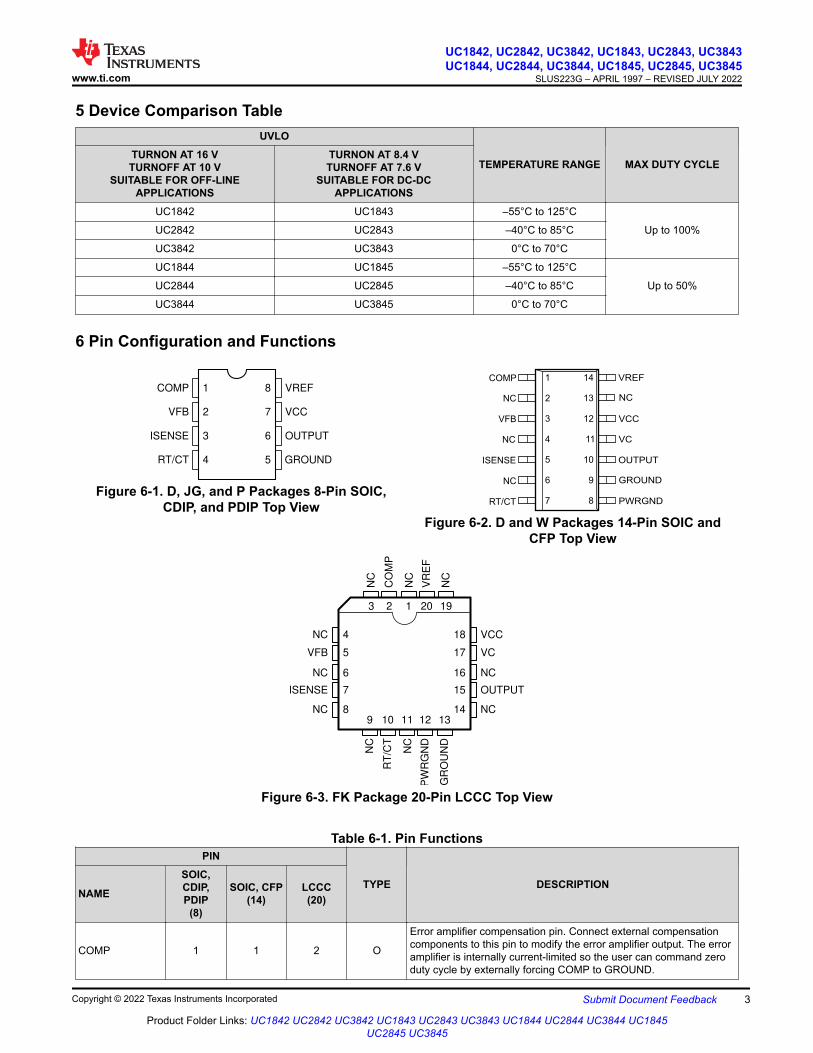
5 Device Comparison TableUVLO
TEMPERATURE RANGE MAX DUTY CYCLETURNON AT 16 VTURNOFF AT 10 V
SUITABLE FOR OFF-LINE APPLICATIONS
TURNON AT 8.4 VTURNOFF AT 7.6 V
SUITABLE FOR DC-DC APPLICATIONS
UC1842 UC1843 –55°C to 125°C
Up to 100%UC2842 UC2843 –40°C to 85°C
UC3842 UC3843 0°C to 70°C
UC1844 UC1845 –55°C to 125°C
Up to 50%UC2844 UC2845 –40°C to 85°C
UC3844 UC3845 0°C to 70°C
6 Pin Configuration and Functions
OUTPUT
VCC
VREF
GROUND
VFB
COMP
ISENSE
RT/CT
1
2
3
4
8
7
6
5
Figure 6-1. D, JG, and P Packages 8-Pin SOIC, CDIP, and PDIP Top View
1
2
3
4
5
6
7
14
13
12
11
10
9
8
VCC
VC
PWRGND
COMP
NC
VFB
NC
ISENSE
NC
RT/CT
GROUND
OUTPUT
VREF
NC
Figure 6-2. D and W Packages 14-Pin SOIC and CFP Top View
9 10 11 12 13
3 2 1 20 19
18
17
16
15
14
4
5
6
7
8
VCC
VC
NC
OUTPUT
NC
NC
VFB
NC
ISENSE
NC
NC
RT
/CT
NC
PW
RG
ND
GR
OU
ND
NC
CO
MP
NC
VR
EF
NC
Figure 6-3. FK Package 20-Pin LCCC Top View
Table 6-1. Pin FunctionsPIN
TYPE DESCRIPTIONNAME
SOIC, CDIP, PDIP(8)
SOIC, CFP(14)
LCCC(20)
COMP 1 1 2 O
Error amplifier compensation pin. Connect external compensation components to this pin to modify the error amplifier output. The error amplifier is internally current-limited so the user can command zero duty cycle by externally forcing COMP to GROUND.
www.ti.com
UC1842, UC2842, UC3842, UC1843, UC2843, UC3843UC1844, UC2844, UC3844, UC1845, UC2845, UC3845
SLUS223G – APRIL 1997 – REVISED JULY 2022
Copyright © 2022 Texas Instruments Incorporated Submit Document Feedback 3
Product Folder Links: UC1842 UC2842 UC3842 UC1843 UC2843 UC3843 UC1844 UC2844 UC3844 UC1845 UC2845 UC3845

Table 6-1. Pin Functions (continued)PIN
TYPE DESCRIPTIONNAME
SOIC, CDIP, PDIP(8)
SOIC, CFP(14)
LCCC(20)
GROUND 5 9 13 G Analog ground. For device packages without PWRGND, GROUND functions as both power ground and analog ground.
PWRGND — 8 12 G Power ground. For device packages without PWRGND, GROUND functions as both power ground and analog ground
ISENSE 3 5 7 I
Primary-side current sense pin. Connect to current sensing resistor. The PWM uses this signal to terminate the OUTPUT switch conduction. A voltage ramp can be applied to this pin to run the device with a voltage-mode control configuration.
NC — 2, 4, 6, 131, 3, 4, 6, 8, 9, 11,
14, 16, 19— Do not connect
OUTPUT 6 10 15 O
OUTPUT is the gate drive for the external MOSFET. OUTPUT is the output of the on-chip driver stage intended to directly drive a MOSFET. Peak currents of up to 1 A are sourced and sunk by this pin. OUTPUT is actively held low when VCC is below the turnon threshold.
RT/CT 4 7 10 I/O
Fixed frequency oscillator set point. Connect timing resistor, RRT, to VREF and timing capacitor, CCT, to GROUND from this pin to set the switching frequency. For best performance, keep the timing capacitor lead to the device GROUND as short and direct as possible. If possible, use separate ground traces for the timing capacitor and all other functions.The frequency of the oscillator can be estimated with the following equations:
fOSC
=
1.72
RRT× C
CT
(1)
where fOSC is in Hertz, RRT is in Ohms and CCT is in Farads. Never use a timing resistor less than 5 kΩ. The frequency of the OUTPUT gate drive of the UCx842 and UCx843, fSW, is equal to fOSC at up to 100% duty cycle; the frequency of the UCx844 and UCx845 is equal to half of the fOSC frequency at up to 50% duty cycle.
VC — 11 17 I
Bias supply input for the output gate drive. For PWM controllers that do not have this pin, the gate driver is biased from the VCC pin. VC must have a bypass capacitor at least 10 times greater than the gate capacitance of the main switching FET used in the design.
VCC 7 12 18 I
Analog controller bias input that provides power to the device. Total VCC current is the sum of the quiescent VCC current and the average OUTPUT current. Knowing the switching frequency and the MOSFET gate charge, Qg, the average OUTPUT current can be calculated from:
IOUTPUT = Qg × fSW (2)
A bypass capacitor, typically 0.1 µF, connected directly to GROUND with minimal trace length, is required on this pin. An additional bypass capacitor at least 10 times greater than the gate capacitance of the main switching FET used in the design is also required on VCC.
VFB 2 3 5 I Inverting input to the internal error amplifier. VFB is used to control the power converter voltage-feedback loop for stability.
UC1842, UC2842, UC3842, UC1843, UC2843, UC3843UC1844, UC2844, UC3844, UC1845, UC2845, UC3845SLUS223G – APRIL 1997 – REVISED JULY 2022 www.ti.com
4 Submit Document Feedback Copyright © 2022 Texas Instruments Incorporated
Product Folder Links: UC1842 UC2842 UC3842 UC1843 UC2843 UC3843 UC1844 UC2844 UC3844 UC1845 UC2845 UC3845

Table 6-1. Pin Functions (continued)PIN
TYPE DESCRIPTIONNAME
SOIC, CDIP, PDIP(8)
SOIC, CFP(14)
LCCC(20)
VREF 8 14 20 O
5-V reference voltage. VREF is used to provide charging current to the oscillator timing capacitor through the timing resistor. It is important for reference stability that VREF is bypassed to GROUND with a ceramic capacitor connected as close to the pin as possible. A minimum value of 0.1-µF ceramic is required. Additional VREF bypassing is required for external loads on VREF.
www.ti.com
UC1842, UC2842, UC3842, UC1843, UC2843, UC3843UC1844, UC2844, UC3844, UC1845, UC2845, UC3845
SLUS223G – APRIL 1997 – REVISED JULY 2022
Copyright © 2022 Texas Instruments Incorporated Submit Document Feedback 5
Product Folder Links: UC1842 UC2842 UC3842 UC1843 UC2843 UC3843 UC1844 UC2844 UC3844 UC1845 UC2845 UC3845
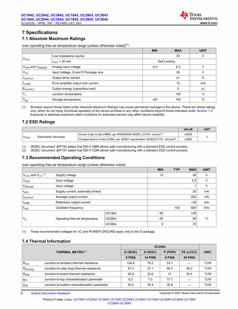
7 Specifications7.1 Absolute Maximum Ratingsover operating free-air temperature range (unless otherwise noted)(1)
MIN MAX UNIT
VVCCLow impedance source 30 V
IVCC < 30 mA Self Limiting
VVFB and VISENSE Analog input voltage –0.3 6.3 V
VVC Input Voltage, Q and D Package only 30 V
IOUTPUT Output drive current ±1 A
ICOMP Error amplifier output sink current 10 mA
EOUTPUT Output energy (capacitive load) 5 µJ
TJ Junction temperature 150 °C
Tstg Storage temperature –65 150 °C
(1) Stresses beyond those listed under Absolute Maximum Ratings may cause permanent damage to the device. These are stress ratings only, which do not imply functional operation of the device at these or any other conditions beyond those indicated under Section 7.3. Exposure to absolute-maximum-rated conditions for extended periods may affect device reliability.
7.2 ESD RatingsVALUE UNIT
V(ESD) Electrostatic dischargeHuman body model (HBM), per ANSI/ESDA/JEDEC JS-001, all pins(1) ±3000
VCharged device model (CDM), per JEDEC specification JESD22-C101, all pins(2) ±3000
(1) JEDEC document JEP155 states that 500-V HBM allows safe manufacturing with a standard ESD control process.(2) JEDEC document JEP157 states that 250-V CDM allows safe manufacturing with a standard ESD control process.
7.3 Recommended Operating Conditionsover operating free-air temperature range (unless otherwise noted)
MIN TYP MAX UNITVVCC and VVC (1) Supply voltage 12 28 V
VVFB Input voltage 2.5 V
VISENSE Input voltage 1 V
IVCC Supply current, externally limited 25 mA
IOUTPUT Average output current 200 mA
IVREF Reference output current –20 mA
fOSC Oscillator frequency 100 500 kHz
TA Operating free-air temperature
UC184x –55 125
°CUC284x –40 85
UC384x 0 70
(1) These recommended voltages for VC and POWER GROUND apply only to the D package.
7.4 Thermal Information
THERMAL METRIC(1)
UCx84xUNITD (SOIC) D (SOIC) P (PDIP) FK (LCCC)
8 PINS 14 PINS 8 PINS 20 PINSRθJA Junction-to-ambient thermal resistance 104.8 78.2 53.7 — °C/W
RθJC(top) Junction-to-case (top) thermal resistance 47.3 37.1 46.7 36.2 °C/W
RθJB Junction-to-board thermal resistance 45.9 32.6 31 35.4 °C/W
ψJT Junction-to-top characterization parameter 8.2 7.3 17.1 — °C/W
ψJB Junction-to-bottom characterization parameter 45.2 32.4 30.9 — °C/W
UC1842, UC2842, UC3842, UC1843, UC2843, UC3843UC1844, UC2844, UC3844, UC1845, UC2845, UC3845SLUS223G – APRIL 1997 – REVISED JULY 2022 www.ti.com
6 Submit Document Feedback Copyright © 2022 Texas Instruments Incorporated
Product Folder Links: UC1842 UC2842 UC3842 UC1843 UC2843 UC3843 UC1844 UC2844 UC3844 UC1845 UC2845 UC3845

7.4 Thermal Information (continued)
THERMAL METRIC(1)
UCx84xUNITD (SOIC) D (SOIC) P (PDIP) FK (LCCC)
8 PINS 14 PINS 8 PINS 20 PINSRθJC(bottom) Junction-to-case (bottom) thermal resistance — — — 4.1 °C/W
(1) For more information about traditional and new thermal metrics, see the Semiconductor and IC Package Thermal Metrics application report.
7.5 Electrical Characteristicsover operating free-air temperature range (unless otherwise noted) –55°C ≤ TA ≤ 125°C for the UC184x; –40°C ≤ TA ≤ 85°C for the UC284x, 0°C ≤ TA ≤ 70°C for the UC384x, VVCC = 15 V(2); 0.1 µF capacitor from VCC to GROUND, 0.1 µF capacitor from VREF to GROUND, RRT = 10 kΩ; CCT = 3.3 nF, TJ = TA.
PARAMETER TEST CONDITIONS MIN TYP MAX UNITREFERENCE SECTION
VVREF Reference voltage IVREF = 1 mA, TJ = 25°C
UC184x and UC284x
4.95 5 5.05V
UC384x 4.9 5 5.1
Line regulation 12 ≤ VCC ≤ 25 V 6 20 mV
Load regulation 1 ≤ IVREF ≤ 20 mA 6 25 mV
Temperature stability See (1) (3) 0.2 0.4 mV/°C
Total output variation Line, load, temperature (1)
UC184x and UC284x
4.9 5.1V
UC384x 4.82 5.18
Output noise voltage 10 Hz ≤ fOSC ≤ 10 kHz, (1) TJ = 25°C 50 μV
Long term stability TA = 125°C, 1000 Hrs (1) 5 25 mV
Output short circuit –30 –100 –180 mA
OSCILLATOR SECTIONfOSC Initial accuracy TJ = 25°C(5) 47 52 57 kHz
Voltage stability 12 ≤ VCC ≤ 25 V 0.2% 1%
Temperature stability TMIN ≤ TA ≤ TMAX (1) 5%
VRT/CT Amplitude Peak-to-peak (1) 1.7 V
ERROR AMPLIFIER SECTION
VVFB Input voltage VCOMP = 2.5 V
UC184x and UC284x
2.45 2.5 2.55V
UC384x 2.42 2.5 2.58
IVFB Input bias current
UC184x and UC284x
–1µA
UC384x –2
AVOL 2 ≤ VCOMP ≤ 4 V 65 90 dB
Unity gain bandwidth TJ = 25°C (1) 0.7 1 MHz
PSRR Power supply rejection ratio 12 ≤ VCC ≤ 25 V 60 70 dB
I(snk) COMP sink current VVFB = 2.7 V, VCOMP = 1.1 V 2 6mA
I(src) COMP source current VVFB = 2.3 V, VCOMP = 5 V –0.5 –0.8
VCOMP High High-level output voltage VVFB = 2.3 V, RL = 15-kΩ COMP to GROUND 5 6
VVCOMP Low Low-level output voltage VVFB = 2.7 V, RL = 15-kΩ COMP to VREF 0.7 1.1
CURRENT SENSE SECTION
www.ti.com
UC1842, UC2842, UC3842, UC1843, UC2843, UC3843UC1844, UC2844, UC3844, UC1845, UC2845, UC3845
SLUS223G – APRIL 1997 – REVISED JULY 2022
Copyright © 2022 Texas Instruments Incorporated Submit Document Feedback 7
Product Folder Links: UC1842 UC2842 UC3842 UC1843 UC2843 UC3843 UC1844 UC2844 UC3844 UC1845 UC2845 UC3845

7.5 Electrical Characteristics (continued)over operating free-air temperature range (unless otherwise noted) –55°C ≤ TA ≤ 125°C for the UC184x; –40°C ≤ TA ≤ 85°C for the UC284x, 0°C ≤ TA ≤ 70°C for the UC384x, VVCC = 15 V(2); 0.1 µF capacitor from VCC to GROUND, 0.1 µF capacitor from VREF to GROUND, RRT = 10 kΩ; CCT = 3.3 nF, TJ = TA.
PARAMETER TEST CONDITIONS MIN TYP MAX UNITACS Gain See (4) (6) 2.85 3 3.15 V/V
VISENSE Maximum input signal VCOMP = 5 V (4) 0.9 1 1.1 V
PSRR Power supply rejection ratio 12 V ≤ VVCC ≤ 25 V (1) (4) 70 dB
IISENSE Input bias current –2 –10 µA
tDLY Delay to output VISENSE stepped from 0 V to 2 V (1) 150 300 ns
OUTPUT SECTION
VOUT Low Low-level OUTPUT voltageISINK = 20 mA 0.1 0.4
VISINK = 200 mA 1.5 2.2
VOUT High High-level OUTPUT voltageISOURCE = 20 mA 13 13.5
VISOURCE = 200 mA 12 13.5
tRISE Rise time (1) COUTPUT = 1 nF, TJ = 25°C 50 150 ns
tFALL Fall time (1) COUTPUT = 1 nF, TJ = 25°C, 50 150 ns
UNDERVOLTAGE LOCKOUT (UVLO)
VCCON Enable threshold
UC1842/4 and UC2842/4 15 16 17
VUC3842/4 14.5 16 17.5
UCx843/5 7.8 8.4 9
VCCOFF UVLO off threshold
UC1842/4 and UC2842/4 9 10 11
VUC3842/4 8.5 10 11.5
UCx843/5 7 7.6 8.2
PWM
DMAX Maximum duty cycle
UCx842/3 95% 97% 100%
UC1844/5 and UC2844/5 46% 48% 50%
UC3844/5 47% 48% 50%
DMIN Minimum duty cycle 0%
TOTAL STANDBY CURRENTIVCC Start-up current 0.5 1
mAIVCC Operating supply current VVFB = VISENSE= 0 V 11 17
VCC Zener voltage IVCC = 25 mA 30 34 V
(1) Specified by design. Not production tested.(2) Adjust VCC above the start threshold before setting at 15 V(3) Temperature stability, sometimes referred to as average temperature coefficient, is described by the equation:
Temp Stability =VREF:max ; F VREF:min ;
TJ:max ; F TJ:min ;
VREFmin and VREFmax are the maximum and minimum reference voltages measured over the appropriate temperature range. Note that the extremes in voltage do not necessarily occur at the extremes in temperature.
(4) Parameter measured at trip point of latch with VFB = 0 V.(5) OUTPUT switching frequency, fSW, equals the oscillator frequency, fOSC, for the UCx842 and UCx843. OUTPUT switching frequency,
fSW, is one half oscillator frequency, fOSC, for the UCx844 and UCx845.(6) Gain defined as: A = ΔVCOMP/ΔVISENSE, 0 V ≤ VISENSE ≤ 0.8 V.
UC1842, UC2842, UC3842, UC1843, UC2843, UC3843UC1844, UC2844, UC3844, UC1845, UC2845, UC3845SLUS223G – APRIL 1997 – REVISED JULY 2022 www.ti.com
8 Submit Document Feedback Copyright © 2022 Texas Instruments Incorporated
Product Folder Links: UC1842 UC2842 UC3842 UC1843 UC2843 UC3843 UC1844 UC2844 UC3844 UC1845 UC2845 UC3845

7.6 Typical Characteristics
Temperature (C)
I DIS
CH
AR
GE (
mA
)
-75 -50 -25 0 25 50 75 100 125 1507.4
7.6
7.8
8
8.2
8.4
8.6
8.8
9
9.2
D001
Figure 7-1. Oscillator Discharge Current vs Temperature for VCC = 15 V and VOSC = 2 V
VO, Error Amp Output Voltage (V)
VT
H, C
urr
ent S
ense Input T
hre
shold
(V
)
1 1.5 2 2.5 3 3.5 4 4.5 5 5.5 60
0.1
0.2
0.3
0.4
0.5
0.6
0.7
0.8
0.9
1
1.1
D005
TA = 125qCTA = 25qCTA = 55qC
Figure 7-2. Current Sense Input Threshold vs Error Amplifier Output Voltage for VCC = 15 V
Freq (Hz)
Ga
in (
dB
)
10 100 1000 10000 100000 1000000 1E+7-20 -100
0 -50
20 0
40 50
60 100
80 150
100 200
D003
GainPhase
Figure 7-3. Error Amplifier Open-Loop Gain and Phase vs Frequency, VCC = 15 V, RL = 100 kΩ, and TA = 25 °C
IO, Output Load Current (mA)
So
urc
e S
atu
ratio
n V
olta
ge
(V
)
Sin
k S
atu
ratio
n V
olta
ge
(V
)
0 100 200 300 400 500 600 700 800-10 0
-9 1
-8 2
-7 3
-6 4
-5 5
-4 6
-3 7
-2 8
-1 9
0 10
D005
Source Saturation at 25 CSource Saturation at -55 CSink Saturation at -55 CSink Saturation at 25 C
Figure 7-4. OUTPUT Saturation Voltage vs Load Current for VCC = 15 V with 5-ms Input Pulses
Temperature (C)
I SC (
mA
)
-75 -50 -25 0 25 50 75 100 125 15040
60
80
100
120
140
160
180
D006
Figure 7-5. VREF Short-Circuit Current vs Temperature for VCC = 15 V
Source Current (mA)
Re
fere
nce
Vo
lta
ge
De
lta
(m
V)
0 20 40 60 80 100 120 140 160-60
-50
-40
-30
-20
-10
0
D007
Ta = 125 CTa = 25 CTa = -40 C
Figure 7-6. VREF Voltage vs Source Current
www.ti.com
UC1842, UC2842, UC3842, UC1843, UC2843, UC3843UC1844, UC2844, UC3844, UC1845, UC2845, UC3845
SLUS223G – APRIL 1997 – REVISED JULY 2022
Copyright © 2022 Texas Instruments Incorporated Submit Document Feedback 9
Product Folder Links: UC1842 UC2842 UC3842 UC1843 UC2843 UC3843 UC1844 UC2844 UC3844 UC1845 UC2845 UC3845

7.6 Typical Characteristics (continued)
Temperature (C)
VR
EF (
V)
-75 -50 -25 0 25 50 75 100 125 1504.8
4.85
4.9
4.95
5
5.05
5.1
5.15
5.2
D008
Figure 7-7. VREF Voltage vs Temperature
0
4
Sa
tura
tio
n V
olta
ge
(V
)
Output Current (A)
0.01 0.1 1
1
2
3
Source, TA = 25°C
Sink, TA = 25°C
Source, TA = ±55°C
Sink, TA = ±55°C
Figure 7-8. Output Saturation
CCT (nF)
t DE
AD
TIM
E (P
s)
1 5 10 50 1000.3
0.5
1
5
10
3030
D006
Figure 7-9. Dead Time vs Timing Capacitance, CCT
100
20
2
1
1 M
Frequency (Hz)
100 k
Tim
ing
Re
sis
tan
ce
(N
)
10 k100 1000
10
50
5
CCT (nF)
100
47
22
10
4.7
2.2
1
Figure 7-10. Timing Resistance, RRT, vs Frequency
UC1842, UC2842, UC3842, UC1843, UC2843, UC3843UC1844, UC2844, UC3844, UC1845, UC2845, UC3845SLUS223G – APRIL 1997 – REVISED JULY 2022 www.ti.com
10 Submit Document Feedback Copyright © 2022 Texas Instruments Incorporated
Product Folder Links: UC1842 UC2842 UC3842 UC1843 UC2843 UC3843 UC1844 UC2844 UC3844 UC1845 UC2845 UC3845
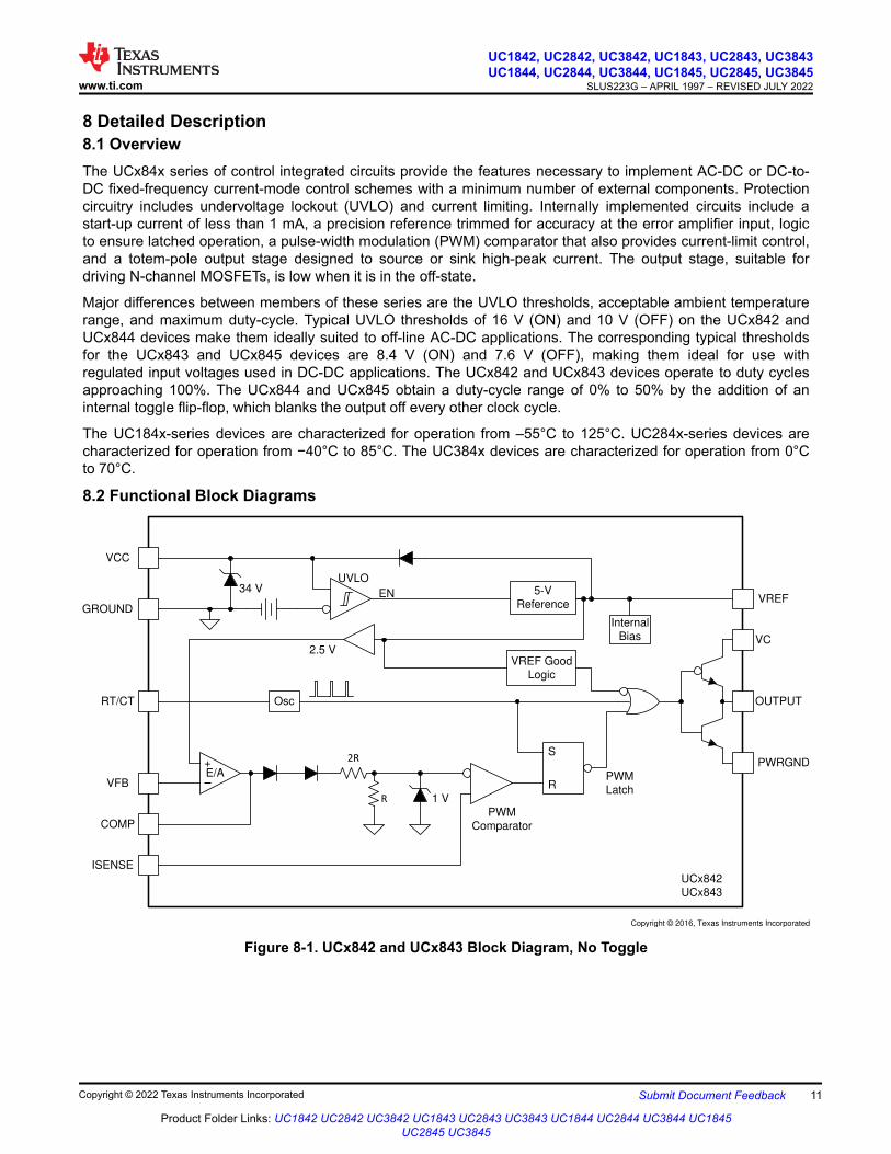
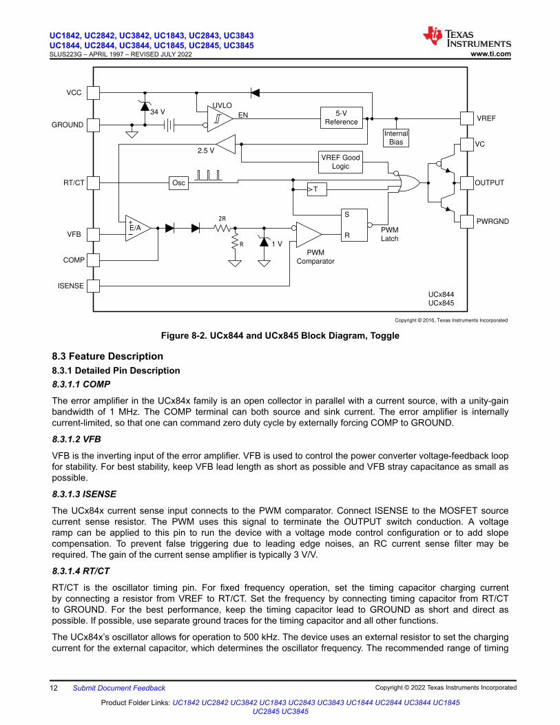
8 Detailed Description8.1 OverviewThe UCx84x series of control integrated circuits provide the features necessary to implement AC-DC or DC-to-DC fixed-frequency current-mode control schemes with a minimum number of external components. Protection circuitry includes undervoltage lockout (UVLO) and current limiting. Internally implemented circuits include a start-up current of less than 1 mA, a precision reference trimmed for accuracy at the error amplifier input, logic to ensure latched operation, a pulse-width modulation (PWM) comparator that also provides current-limit control, and a totem-pole output stage designed to source or sink high-peak current. The output stage, suitable for driving N-channel MOSFETs, is low when it is in the off-state.
Major differences between members of these series are the UVLO thresholds, acceptable ambient temperature range, and maximum duty-cycle. Typical UVLO thresholds of 16 V (ON) and 10 V (OFF) on the UCx842 and UCx844 devices make them ideally suited to off-line AC-DC applications. The corresponding typical thresholds for the UCx843 and UCx845 devices are 8.4 V (ON) and 7.6 V (OFF), making them ideal for use with regulated input voltages used in DC-DC applications. The UCx842 and UCx843 devices operate to duty cycles approaching 100%. The UCx844 and UCx845 obtain a duty-cycle range of 0% to 50% by the addition of an internal toggle flip-flop, which blanks the output off every other clock cycle.
The UC184x-series devices are characterized for operation from –55°C to 125°C. UC284x-series devices are characterized for operation from −40°C to 85°C. The UC384x devices are characterized for operation from 0°C to 70°C.
8.2 Functional Block Diagrams
UCx842
UCx843
34 V 5-V
ReferenceEN
VREF Good
Logic
Internal
Bias
UVLO
Osc
S
RPWM
LatchR 1 V
+E/A
VCC
GROUND
RT/CT
VFB
COMP
ISENSE
PWM
Comparator
VREF
OUTPUT
VC
PWRGND2R
2.5 V
Copyright © 2016, Texas Instruments Incorporated
Figure 8-1. UCx842 and UCx843 Block Diagram, No Toggle
www.ti.com
UC1842, UC2842, UC3842, UC1843, UC2843, UC3843UC1844, UC2844, UC3844, UC1845, UC2845, UC3845
SLUS223G – APRIL 1997 – REVISED JULY 2022
Copyright © 2022 Texas Instruments Incorporated Submit Document Feedback 11
Product Folder Links: UC1842 UC2842 UC3842 UC1843 UC2843 UC3843 UC1844 UC2844 UC3844 UC1845 UC2845 UC3845
34 V 5-V
ReferenceEN
VREF Good
Logic
Internal
Bias
UVLO
Osc
S
RPWM
LatchR 1 V
+E/A
VCC
GROUND
RT/CT
VFB
COMP
ISENSE
PWM
Comparator
VREF
OUTPUT
VC
PWRGND
UCx844
UCx845
2R
T
2.5 V
Copyright © 2016, Texas Instruments Incorporated
Figure 8-2. UCx844 and UCx845 Block Diagram, Toggle
8.3 Feature Description8.3.1 Detailed Pin Description8.3.1.1 COMP
The error amplifier in the UCx84x family is an open collector in parallel with a current source, with a unity-gain bandwidth of 1 MHz. The COMP terminal can both source and sink current. The error amplifier is internally current-limited, so that one can command zero duty cycle by externally forcing COMP to GROUND.
8.3.1.2 VFB
VFB is the inverting input of the error amplifier. VFB is used to control the power converter voltage-feedback loop for stability. For best stability, keep VFB lead length as short as possible and VFB stray capacitance as small as possible.
8.3.1.3 ISENSE
The UCx84x current sense input connects to the PWM comparator. Connect ISENSE to the MOSFET source current sense resistor. The PWM uses this signal to terminate the OUTPUT switch conduction. A voltage ramp can be applied to this pin to run the device with a voltage mode control configuration or to add slope compensation. To prevent false triggering due to leading edge noises, an RC current sense filter may be required. The gain of the current sense amplifier is typically 3 V/V.
8.3.1.4 RT/CT
RT/CT is the oscillator timing pin. For fixed frequency operation, set the timing capacitor charging current by connecting a resistor from VREF to RT/CT. Set the frequency by connecting timing capacitor from RT/CT to GROUND. For the best performance, keep the timing capacitor lead to GROUND as short and direct as possible. If possible, use separate ground traces for the timing capacitor and all other functions.
The UCx84x’s oscillator allows for operation to 500 kHz. The device uses an external resistor to set the charging current for the external capacitor, which determines the oscillator frequency. The recommended range of timing
UC1842, UC2842, UC3842, UC1843, UC2843, UC3843UC1844, UC2844, UC3844, UC1845, UC2845, UC3845SLUS223G – APRIL 1997 – REVISED JULY 2022 www.ti.com
12 Submit Document Feedback Copyright © 2022 Texas Instruments Incorporated
Product Folder Links: UC1842 UC2842 UC3842 UC1843 UC2843 UC3843 UC1844 UC2844 UC3844 UC1845 UC2845 UC3845
resistor values is between 5 kΩ and 100 kΩ; the recommended range of timing capacitor values is between 1 nF and 100 nF.
fOSC
=
1.72
RRT× C
CT
(3)
In this equation, the switching frequency, fSW is in Hz, RRT is in Ω, and CCT is in Farads.
8.3.1.5 GROUND
GROUND is the signal and power returning ground. TI recommends separating the signal return path and the high current gate driver path so that the signal is not affected by the switching current.
8.3.1.6 OUTPUT
The high-current bipolar totem-pole output of the UCx84x devices sinks or sources up to 1-A peak of current. The OUTPUT pin can directly drive a MOSFET. The OUTPUT of the UCx842 and UCx843 devices switches at the same frequency as the oscillator and can operate near 100% duty cycle. In the UCx844 and UCx845 devices, the switching frequency of OUTPUT is one-half that of the oscillator due to an internal T flipflop. This limits the maximum duty cycle in the UCx844 and UCx845 to < 50%. Schottky diodes may be necessary on the OUTPUT pin to prevent overshoot and undershoot due to high impedance to the supply rail and to ground, respectively. A bleeder resistor, placed between the gate and the source of the MOSFET, should be used to prevent activating the power switch with extraneous leakage currents during undervoltage lockout. An external clamp circuit may be necessary to prevent overvoltage stress on the MOSFET gate when VCC exceeds the gate voltage rating.
8.3.1.7 VCC
VCC is the power input connection for this device. In normal operation, power VCC through a current-limiting resistor. Although quiescent VCC current is only 0.5 mA, the total supply current is higher, depending on the OUTPUT current. Total VCC current is the sum of quiescent VCC current and the average OUTPUT current. Knowing the operating frequency and the MOSFET gate charge (Qg), average OUTPUT current can be calculated from Equation 4.
IOUTPUT = Qg × fSW (4)
The UCx84x has a VCC supply voltage clamp of 34 V typical, but the absolute maximum value for VCC from a low-impedance source is 30 V. For applications that have a higher input voltage than the recommended VCC voltage, place a resistor in series with VCC to increase the source impedance. The maximum value of this resistor is calculated with Equation 5.
RVCC :max ; =VIN:min ; F VVCC :max ;IVCC + kQg × fSW o
(5)
In Equation 5, VIN(min) is the minimum voltage that is used to supply VCC, VVCC(max) is the maximum VCC clamp voltage and IVCC is the IC supply current without considering the gate driver current and Qg is the external power MOSFET gate charge and fSW is the switching frequency.
The turnon and turnoff thresholds for the UCx84x family are significantly different: 16 V and 10 V for the UCx842 and UCx844; 8.4 V and 7.6 V for the UCx843 and UCx855. To ensure against noise related problems, filter VCC with an electrolytic and bypass with a ceramic capacitor to ground. Keep the capacitors close to the IC pins.
8.3.1.8 VREF
VREF is the voltage reference for the error amplifier and also for many other internal circuits in the IC. The high-speed switching logic uses VREF as the logic power supply. The 5-V reference tolerance is ±2% for the UCx84x family. The output short-circuit current is 30 mA. For reference stability and to prevent noise problems with high-speed switching transients, bypass VREF to ground with a ceramic capacitor close to the IC package.
www.ti.com
UC1842, UC2842, UC3842, UC1843, UC2843, UC3843UC1844, UC2844, UC3844, UC1845, UC2845, UC3845
SLUS223G – APRIL 1997 – REVISED JULY 2022
Copyright © 2022 Texas Instruments Incorporated Submit Document Feedback 13
Product Folder Links: UC1842 UC2842 UC3842 UC1843 UC2843 UC3843 UC1844 UC2844 UC3844 UC1845 UC2845 UC3845

A minimum of 0.1-µF ceramic capacitor is required. Additional VREF bypassing is required for external loads on the reference. An electrolytic capacitor may also be used in addition to the ceramic capacitor.
When VCC is greater than 1 V and less than the UVLO threshold, a 5-kΩ resistor pulls VREF to ground. VREF can be used as a logic output indicating power-system status because when VCC is lower than the UVLO threshold, VREF is held low.
8.3.2 Pulse-by-Pulse Current Limiting
Pulse-by-pulse limiting is inherent in the current mode control scheme. An upper limit on the peak current can be established by simply clamping the error voltage. Accurate current limiting allows optimization of magnetic and power semiconductor elements while ensuring reliable supply operation.
8.3.3 Current-Sense
An external series resistor, RCS, senses the current and converts this current into a voltage that becomes the input to the ISENSE pin. The ISENSE pin is the noninverting input to the PWM comparator. The ISENSE input is compared to a signal proportional to the error amplifier output voltage; the gain of the current sense amplifier is typically 3 V/V. The peak ISENSE current is determined by Equation 6:
ISENSE =VISENSE
RCS
(6)
The typical value for VISENSE is 1 V. A small RC filter, RCSF and CCSF, may be required to suppress switch transients caused by the reverse recovery of a secondary side diode or equivalent capacitive loading in addition to parasitic circuit impedances. The time constant of this filter should be considerably less than the switching period of the converter.
ISENSE
GROUND
COMP
2 R
R
CCSF
RCSF
RCS
PWM
Comparator
1 V
Error
Amplifier
ISENSE
Copyright © 2016, Texas Instruments Incorporated
Figure 8-3. Current-Sense Circuit Schematic
8.3.4 Error Amplifier With Low Output Resistance
The error amplifier output is an open collector in parallel with a current source. With a low output resistance, various impedance networks may be used on the compensation pin input for error amplifier feedback. The error amplifier output, COMP, is frequently used as a control port for secondary-side regulation by using an external secondary-side adjustable voltage regulator, such as a TL431, to send an error signal across the secondary-to-primary isolation boundary through an opto-isolator, in this configuration connect the COMP pin directly to the opto-isolator feedback. On the primary side, the inverting input to the UCx48x error amplifier, VFB, should be connected to GROUND. With VFB tied to GROUND, the error amplifier output, COMP, is forced to its
UC1842, UC2842, UC3842, UC1843, UC2843, UC3843UC1844, UC2844, UC3844, UC1845, UC2845, UC3845SLUS223G – APRIL 1997 – REVISED JULY 2022 www.ti.com
14 Submit Document Feedback Copyright © 2022 Texas Instruments Incorporated
Product Folder Links: UC1842 UC2842 UC3842 UC1843 UC2843 UC3843 UC1844 UC2844 UC3844 UC1845 UC2845 UC3845

high state and sources current, typically 0.8 mA. The opto-isolator must overcome the source current capability to control the COMP pin below the error amplifier output high level, VOH.
For primary-side regulation, configure the inverting input to the error amplifier, VFB, with a resistor divider to provide a signal that is proportional to the converter output voltage being regulated. Add the voltage loop compensation components between VFB and COMP. The internal noninverting input to the error amplifier is trimmed to 2.5 V. For best stability, keep VFB lead length as short as possible and minimize the stray capacitance on VFB.
The internal resistor divider on COMP is maintained at an R:2R ratio, the specific values of these internal resistors should not be critical in any application.
ISENSE
COMP
2 R
RPWM
Comparator
1 V
Error
Amplifier
2.5 V
VFB
0.5 mA
+
sZI
ZF
Error amplifier can source or sink up to 0.5 mA.
Figure 8-4. Error-Amplifier Configuration Schematic
8.3.5 Undervoltage Lockout
The UCx84x devices feature undervoltage lockout protection circuits for controlled operation during power-up and power-down sequences. The UVLO circuit insures that VCC is adequate to make the UCx84x fully operational before enabling the output stage. Undervoltage lockout thresholds for the UCx842, UCx843, UCx844, and UCx845 devices are optimized for two groups of applications: off-line power supplies and DC-DC converters. The 6-V hysteresis in the UCx842 and UCx844 devices prevents VCC oscillations during power sequencing. This wider VCCON to VCCOFF range, make these devices ideally suited to off-line AC input applications. The UCx843 and UCx845 controllers have a much narrower VCCON to VCCOFF hysteresis and may be used in DC to DC applications where the input is considered regulated.
Start-up current is less than 1 mA for efficient bootstrapping from the rectified input of an off-line converter, as illustrated by Figure 8-7. During normal circuit operation, VCC is developed from auxiliary winding NA with DBIAS and CVCC. At start-up, however, CVCC must be charged to 16 V through RSTART. With a start-up current of 1 mA, RSTART can be as large as 100 kΩ and still charge CVCC when VAC = 90 V RMS (low line). Power dissipation in RSTART would then be less than 350 mW even under high line (VAC= 130 V RMS) conditions.
During UVLO the IC draws less than 1 mA of supply current. Once crossing the turnon threshold the IC supply current increases to a maximum of 17 mA, typically 11 mA, During undervoltage lockout, the output driver is biased to a high impedance state and sinks minor amounts of current. A bleeder resistor, placed between the gate and the source of the MOSFET should be used to prevent activating the power switch with extraneous leakage currents during undervoltage lockout.
www.ti.com
UC1842, UC2842, UC3842, UC1843, UC2843, UC3843UC1844, UC2844, UC3844, UC1845, UC2845, UC3845
SLUS223G – APRIL 1997 – REVISED JULY 2022
Copyright © 2022 Texas Instruments Incorporated Submit Document Feedback 15
Product Folder Links: UC1842 UC2842 UC3842 UC1843 UC2843 UC3843 UC1844 UC2844 UC3844 UC1845 UC2845 UC3845

VON (V)
VOFF (V)
16
UCx842
UCx844
UCx843
UCx845
10
8.4
7.6
7VCC ON/OFF Command
to rest of device
Copyright © 2016, Texas Instruments Incorporated
Figure 8-5. UVLO Threshold
< 1 mA
VOFF
< 17 mA
VON
VVCC
IVCC
Figure 8-6. UVLO ON and OFF Profile
VAC
CIN
RSTART
CVCC
VCC
OUTPUT
GROUND0.1 PF
IVCC 1mADBIAS
RCS
NP
NA
NS
Figure 8-7. Providing Power to UCx84x
8.3.6 Oscillator
The oscillator allows for up to 500-kHz switching frequency. The OUTPUT gate drive is the same frequency as the oscillator in the UCx842 and UCx843 devices and can operate near 100% duty cycle. In the UCx844 and UCx845 devices, the frequency of OUTPUT is one-half that of the oscillator due to an internal T flipflop that blanks the output off every other clock cycle, resulting in a maximum duty cycle for these devices of < 50% of the switching frequency. An external resistor, RRT, connected from VREF to RT/CT sets the charging current for the timing capacitor, CCT, which is connected from RT/CT to GROUND. An RRT value greater than 5 kΩ is recommended on RT/CT to set the positive ramp time of the internal oscillator. Using a value of 5 kΩ or greater for RRT maintains a favorable ratio between the internal impedance and the external oscillator set resistor and results in minimal change in frequency over temperature. Using a value of less the recommended minimum value may result in frequency drift over temperature, part tolerances, or process variations.
The peak-to-peak amplitude of the oscillator waveform is 1.7 V in UCx84x devices. The UCx842 and UCx843 have a maximum duty cycle of approximately 100%, whereas the UCx844 and UCx845 are clamped to 50% maximum by an internal toggle flip flop. This duty cycle clamp is advantageous in most flyback and forward converters. For optimum IC performance the dead-time should not exceed 15% of the oscillator clock period. The discharge current, typically 6 mA at room temperature, sets the dead time, see Figure 7-9. During the discharge, or dead time, the internal clock signal blanks the output to the low state. This limits the maximum duty cycle DMAX to:
UC1842, UC2842, UC3842, UC1843, UC2843, UC3843UC1844, UC2844, UC3844, UC1845, UC2845, UC3845SLUS223G – APRIL 1997 – REVISED JULY 2022 www.ti.com
16 Submit Document Feedback Copyright © 2022 Texas Instruments Incorporated
Product Folder Links: UC1842 UC2842 UC3842 UC1843 UC2843 UC3843 UC1844 UC2844 UC3844 UC1845 UC2845 UC3845

DMAX = 1F :tDEADTIME × fOSC ; (7)
Equation 8 applies to UCx842 and UCx843 units because the OUTPUT switches at the same frequency as the oscillator and the maximum duty cycle can be as high as 100%.
DMAX = 1 F ltDEADTIME ×fOSC
2p
(8)
Equation 8 applies to UCx844 and UCx845 units because the OUTPUT switches at half the frequency as the oscillator and the maximum duty cycle can be as high as 50%.
When the power transistor turns off, a noise spike is coupled to the oscillator RT/CT terminal. At high duty cycles, the voltage at RT/CT is approaching its threshold level (approximately 2.7 V, established by the internal oscillator circuit) when this spike occurs. A spike of sufficient amplitude prematurely trips the oscillator. To minimize the noise spike, choose CCT as large as possible, remembering that dead time increases with CCT. It is recommended that CCT never be less than approximately 1000 pF. Often the noise which causes this problem is caused by the OUTPUT being pulled below ground at turnoff by external parasitics. This is particularly true when driving MOSFETs. A Schottky diode clamp from GROUND to OUTPUT prevents such output noise from feeding to the oscillator.
RRT
CCT
VREF
RT/CT
GROUND
Copyright © 2016, Texas Instruments Incorporated
For RRT > 5 kΩ: fOSC
=
1.72
RRT× C
CT
Figure 8-8. Oscillator Section Schematic
8.3.7 Synchronization
The simplest method to force synchronization uses the timing capacitor, CCT, in near standard configuration. Rather than bring CCT to ground directly, a small resistor is placed in series with CCT to ground. This resistor serves as the input for the sync pulse which raises the CCT voltage above the oscillator’s internal upper threshold. The PWM is allowed to run at the frequency set by RRT and CCT until the sync pulse appears. This scheme offers several advantages including having the local ramp available for slope compensation. The UC3842/3/4/5 oscillator must be set to a lower frequency than the sync pulse stream, typically 20% with a 0.5-V pulse applied across the resistor.
www.ti.com
UC1842, UC2842, UC3842, UC1843, UC2843, UC3843UC1844, UC2844, UC3844, UC1845, UC2845, UC3845
SLUS223G – APRIL 1997 – REVISED JULY 2022
Copyright © 2022 Texas Instruments Incorporated Submit Document Feedback 17
Product Folder Links: UC1842 UC2842 UC3842 UC1843 UC2843 UC3843 UC1844 UC2844 UC3844 UC1845 UC2845 UC3845

RRT
CCT
VREF
RT/CT
GROUND
24 O
SYNC
Figure 8-9. Synchronizing the Oscillator
8.3.8 Shutdown Technique
The PWM controller (see Figure 8-10) can be shut down by two methods: either raise the voltage at ISENSE above 1 V or pull the COMP terminal below a voltage two diode drops above ground. Either method causes the output of the PWM comparator to be high (see Figure 8-10). The PWM latch is reset dominant so that the output remains low until the next clock cycle after the shutdown condition at the COMP or ISENSE terminal is removed. In one example, an externally latched shutdown can be accomplished by adding an SCR that resets by cycling VCC below the lower UVLO threshold. At this point, the reference turns off, allowing the SCR to reset.
VREF
ISENSE
SHUTDOWN
30 O
500 O
1 kO
To Current
Sense Resistor
COMP
SHUTDOWN
Figure 8-10. Shutdown Techniques
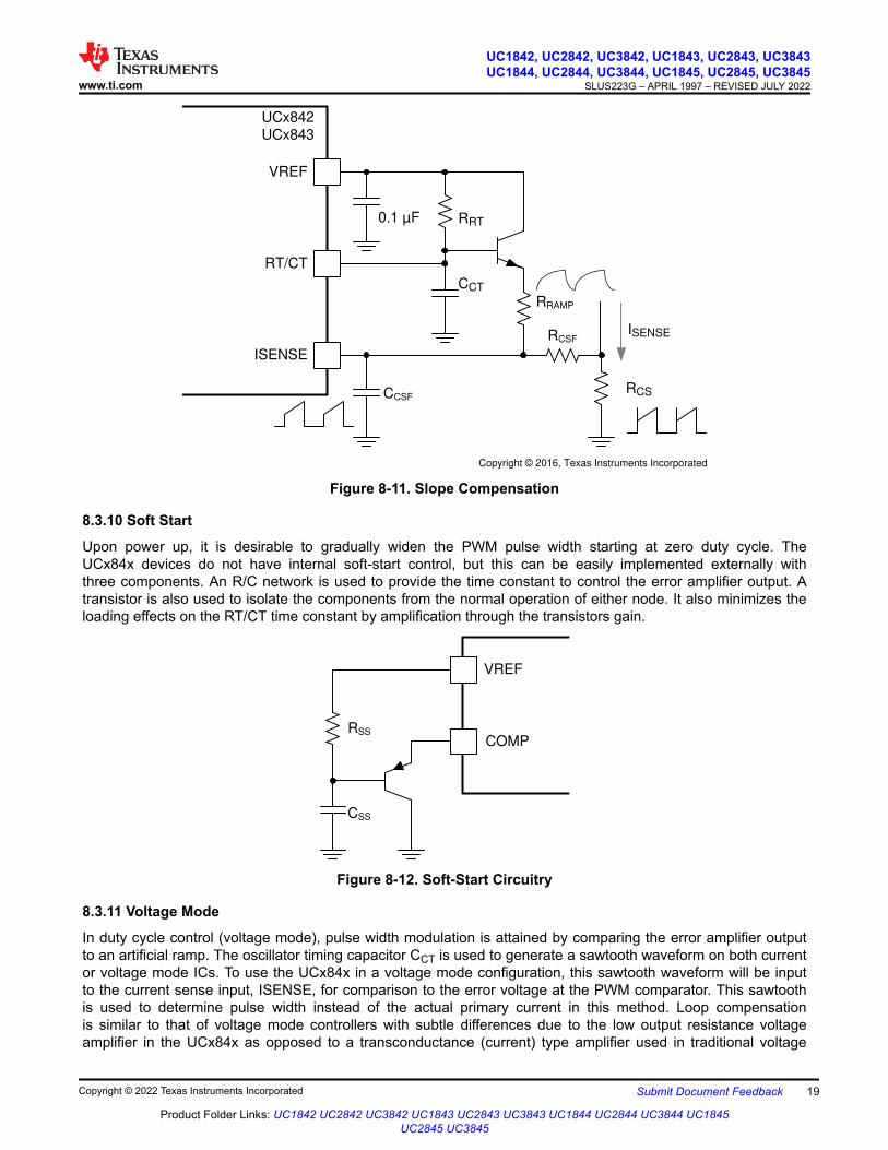
8.3.9 Slope Compensation
A fraction of the oscillator ramp can be summed resistively with the current-sense signal to provide slope compensation for converters requiring duty cycles over 50% (see Figure 8-11). Note that capacitor CCSF forms a filter with RCSF to suppress the leading-edge switch spikes.
UC1842, UC2842, UC3842, UC1843, UC2843, UC3843UC1844, UC2844, UC3844, UC1845, UC2845, UC3845SLUS223G – APRIL 1997 – REVISED JULY 2022 www.ti.com
18 Submit Document Feedback Copyright © 2022 Texas Instruments Incorporated
Product Folder Links: UC1842 UC2842 UC3842 UC1843 UC2843 UC3843 UC1844 UC2844 UC3844 UC1845 UC2845 UC3845
CCT
VREF
RT/CT
ISENSE
UCx842UCx843
0.1 µF RRT
RRAMP
CCSF
RCSF
RCS
ISENSE
Copyright © 2016, Texas Instruments Incorporated
Figure 8-11. Slope Compensation
8.3.10 Soft Start
Upon power up, it is desirable to gradually widen the PWM pulse width starting at zero duty cycle. The UCx84x devices do not have internal soft-start control, but this can be easily implemented externally with three components. An R/C network is used to provide the time constant to control the error amplifier output. A transistor is also used to isolate the components from the normal operation of either node. It also minimizes the loading effects on the RT/CT time constant by amplification through the transistors gain.
VREF
COMP
CSS
RSS
Figure 8-12. Soft-Start Circuitry
8.3.11 Voltage Mode
In duty cycle control (voltage mode), pulse width modulation is attained by comparing the error amplifier output to an artificial ramp. The oscillator timing capacitor CCT is used to generate a sawtooth waveform on both current or voltage mode ICs. To use the UCx84x in a voltage mode configuration, this sawtooth waveform will be input to the current sense input, ISENSE, for comparison to the error voltage at the PWM comparator. This sawtooth is used to determine pulse width instead of the actual primary current in this method. Loop compensation is similar to that of voltage mode controllers with subtle differences due to the low output resistance voltage amplifier in the UCx84x as opposed to a transconductance (current) type amplifier used in traditional voltage
www.ti.com
UC1842, UC2842, UC3842, UC1843, UC2843, UC3843UC1844, UC2844, UC3844, UC1845, UC2845, UC3845
SLUS223G – APRIL 1997 – REVISED JULY 2022
Copyright © 2022 Texas Instruments Incorporated Submit Document Feedback 19
Product Folder Links: UC1842 UC2842 UC3842 UC1843 UC2843 UC3843 UC1844 UC2844 UC3844 UC1845 UC2845 UC3845
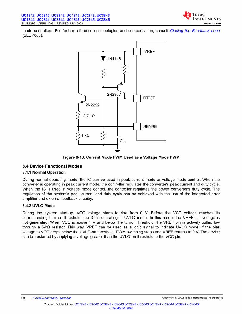
mode controllers. For further reference on topologies and compensation, consult Closing the Feedback Loop (SLUP068).
VREF
RT/CT
CCT
1N4148
2N2907
1 k
2.7 k
ISENSE
2N2222
Figure 8-13. Current Mode PWM Used as a Voltage Mode PWM
8.4 Device Functional Modes8.4.1 Normal Operation
During normal operating mode, the IC can be used in peak current mode or voltage mode control. When the converter is operating in peak current mode, the controller regulates the converter's peak current and duty cycle. When the IC is used in voltage mode control, the controller regulates the power converter's duty cycle. The regulation of the system's peak current and duty cycle can be achieved with the use of the integrated error amplifier and external feedback circuitry.
8.4.2 UVLO Mode
During the system start-up, VCC voltage starts to rise from 0 V. Before the VCC voltage reaches its corresponding turn on threshold, the IC is operating in UVLO mode. In this mode, the VREF pin voltage is not generated. When VCC is above 1 V and below the turnon threshold, the VREF pin is actively pulled low through a 5-kΩ resistor. This way, VREF can be used as a logic signal to indicate UVLO mode. If the bias voltage to VCC drops below the UVLO-off threshold, PWM switching stops and VREF returns to 0 V. The device can be restarted by applying a voltage greater than the UVLO-on threshold to the VCC pin.
UC1842, UC2842, UC3842, UC1843, UC2843, UC3843UC1844, UC2844, UC3844, UC1845, UC2845, UC3845SLUS223G – APRIL 1997 – REVISED JULY 2022 www.ti.com
20 Submit Document Feedback Copyright © 2022 Texas Instruments Incorporated
Product Folder Links: UC1842 UC2842 UC3842 UC1843 UC2843 UC3843 UC1844 UC2844 UC3844 UC1845 UC2845 UC3845

9 Application and ImplementationNote
Information in the following applications sections is not part of the TI component specification, and TI does not warrant its accuracy or completeness. TI’s customers are responsible for determining suitability of components for their purposes, as well as validating and testing their design implementation to confirm system functionality.
9.1 Application InformationThe UCx84x controllers are peak current mode pulse width modulators. These controllers have an onboard amplifier and can be used in isolated and non-isolated power supply design. There is an onboard totem pole gate driver capable of delivering 1 A of peak current. This is a high-speed PWM capable of operating at switching frequencies up to 500 kHz.
9.1.1 Open-Loop Test Fixture
The following application is an open-loop laboratory test fixture. This circuit demonstrates the setup and use of the UCx84x devices and their internal circuitry.
In the open-loop laboratory test fixture (see Figure 9-1), high peak currents associated with loads necessitate careful grounding techniques. Timing and bypass capacitors should be connected close to the GROUND terminal in a single-point ground. The transistor and 5-kΩ potentiometer sample the oscillator waveform and apply an adjustable ramp to the ISENSE terminal.
COMP
VFB
UCx842
ISENSE
RT/CT
1
2
3
4
VREF
VCC
OUTPUT
GROUND
8
7
6
5
0.1 PF
R1
CRTCT
100 N
5 N
ISENSE
Adjust
1 N
E/A
Adjust
4.7 N
4.7 N
0.1 PF
GROUND
1 N
OUTPUT
VREF
VCC
Copyright © 2016, Texas Instruments Incorporated
Figure 9-1. Open-Loop Laboratory Test Fixture
9.2 Typical ApplicationA typical application for the UC2842 in an off-line flyback converter is shown in Figure 9-2. The UC2842 uses an inner current control loop that contains a small current sense resistor which senses the primary inductor current ramp. This current sense resistor transforms the inductor current waveform to a voltage signal that is input directly into the primary side PWM comparator. This inner loop determines the response to input voltage changes. An outer voltage control loop involves comparing a portion of the output voltage to a reference voltage at the input of an error amplifier. When used in an off-line isolated application, the voltage feedback of the
www.ti.com
UC1842, UC2842, UC3842, UC1843, UC2843, UC3843UC1844, UC2844, UC3844, UC1845, UC2845, UC3845
SLUS223G – APRIL 1997 – REVISED JULY 2022
Copyright © 2022 Texas Instruments Incorporated Submit Document Feedback 21
Product Folder Links: UC1842 UC2842 UC3842 UC1843 UC2843 UC3843 UC1844 UC2844 UC3844 UC1845 UC2845 UC3845

isolated output is accomplished using a secondary-side error amplifier and adjustable voltage reference, such as the TL431. The error signal crosses the primary to secondary isolation boundary using an opto-isolator whose collector is connected to the VREF pin and the emitter is connected to VFB. The outer voltage control loop determines the response to load changes.
VIN = 85 VAC to 265 VAC
DBRIDGE
~
~
+±
CIN
180 µF
RSNUB
50 k CSNUB
10 nF
NPNS
NA
DCLAMP
LP =1.5 mHNP:NS = 10NP:NA = 10
COUT
2200 µF
VOUT
12 V,4 A
DOUT
RVCC
22 DBIAS
1
2
3
4
COMP
VFB
ISENSE
RT/CT 5
6
7
8
GROUND
OUTPUT
VCC
VREF
UC2842
RBLEEDER
10 k CVREF
1 µF
CVCC
120 µF
RSTART
100 k
RG
10
RCS
0.75
CSS
RSS
CCSF
100 pF
RCSF
4.2 k
RP
Not Populated
QSW
TL431
RFBU
9.53 k
RFBB
2.49 k
CCOMPz
0.01 µFRCOMPz
88.7 k
10 V
CCOMPp
10 nF
RFBG
4.99 k
RLED
1.3 k
ROPTO
1 k
OPTO-COUPLER
RTLbias
1 k
CVCCbp
0.1 µF
CRAMP
10 nF
RRAMP
24.9 k
RRT
15.4 k
CCT
1000 pF
RCOMPp
10 k
Copyright © 2016, Texas Instruments Incorporated
Figure 9-2. Typical Application Design Example Schematic
9.2.1 Design Requirements
Table 9-1 illustrates a typical set of performance requirements for an off-line flyback converter capable of providing 48 W at 12-V output voltage from a universal AC input. The design uses peak primary current control in a continuous current mode PWM converter.
Table 9-1. Performance RequirementsPARAMETER TEST CONDITIONS MIN NOM MAX UNIT
VIN Input Voltage 85 115/230 265 VRMS
fLINE Line Frequency 47 50/60 63 Hz
VOUT Output Voltage IOUT(min) ≤ IOUT ≤ IOUT(max) 11.75 12 12.25 V
VRIPPLEOutput Ripple Voltage IOUT(min) ≤ IOUT ≤ IOUT(max) 100 mVpp
IOUT Output Current 0 4 A
fSWSwitching Frequency 100 kHz
η Efficiency 85%
UC1842, UC2842, UC3842, UC1843, UC2843, UC3843UC1844, UC2844, UC3844, UC1845, UC2845, UC3845SLUS223G – APRIL 1997 – REVISED JULY 2022 www.ti.com
22 Submit Document Feedback Copyright © 2022 Texas Instruments Incorporated
Product Folder Links: UC1842 UC2842 UC3842 UC1843 UC2843 UC3843 UC1844 UC2844 UC3844 UC1845 UC2845 UC3845

9.2.2 Detailed Design Procedure
This procedure outlines the steps to design an off-line universal input continuous current mode (CCM) flyback converter using the UC2842. See Figure 9-2 for component names referred to in the design procedure.
9.2.2.1 Input Bulk Capacitor and Minimum Bulk Voltage
Bulk capacitance may consist of one or more capacitors connected in parallel, often with some inductance between them to suppress differential-mode conducted noise. The value of the input capacitor sets the minimum bulk voltage; setting the bulk voltage lower by using minimal input capacitance results in higher peak primary currents leading to more stress on the MOSFET switch, the transformer, and the output capacitors. Setting the bulk voltage higher by using a larger input capacitor results in higher peak current from the input source and the capacitor itself will be physically larger. Compromising between size and component stresses determines the acceptable minimum input voltage. The total required value for the primary-side bulk capacitance, CIN, is selected based upon the power level of the converter, POUT, the efficiency target, η, the minimum input voltage, VIN(min), and is chosen to maintain an acceptable minimum bulk voltage level, VBULK(min), using Equation 9.
CIN =
2 × PIN × F0.25 + 1N× arcsinF VBULK (min )
¾2 × VIN(min )GG
k2 × VIN(min )2 F VBULK (min )
2 o × fLINE (min )
(9)
In this equation, VIN(min) is the RMS value of the minimum AC input voltage, 85 VRMS, whose minimum line frequency is denoted as fLINE(min), equal to 47 Hz. Based on the CIN equation, to achieve a minimum bulk voltage of 75 V, assuming 85% converter efficiency, the bulk capacitor should be larger than 126 µF; 180 µF was chosen for the design, taking into consideration component tolerances and efficiency estimation.
9.2.2.2 Transformer Turns Ratio and Maximum Duty Cycle
The transformer design starts with selecting a suitable switching frequency for the given application. The UC2842 is capable of switching up to 500 kHz but considerations such as overall converter size, switching losses, core loss, system compatibility, and interference with communication frequency bands generally determine an optimum frequency that should be used. For this off-line converter, the switching frequency, fSW, is selected to be 110 kHz as a compromise to minimize the transformer size and the EMI filter size, and still have acceptable losses.
The transformer primary to secondary turns ratio, NPS, can be selected based on the desired MOSFET voltage rating and the secondary diode voltage rating. Because the maximum input voltage is 265 VRMS, the peak bulk input voltage can be calculated as shown in Equation 10.
VBULK (max ) = ¾2 × VIN (max ) N 375 V (10)
To minimize the cost of the system, a readily available 650-V MOSFET is selected. Derating the maximum voltage stress on the drain to 80% of its rated value and allowing for a leakage inductance voltage spike of up to 30% of the maximum bulk input voltage, the reflected output voltage should be less than 130 V as shown in Equation 11.
REFLECTED DS(rated) BULK(max)V 0.8 V 1.3 V 130.2V u u (11)
The maximum primary to secondary transformer turns ratio, NPS, for a 12 V output can be selected as
NPS =VREFLECTED
VOUT= 10.85
(12)
A turns ratio of NPS = 10 is used in the design example.
www.ti.com
UC1842, UC2842, UC3842, UC1843, UC2843, UC3843UC1844, UC2844, UC3844, UC1845, UC2845, UC3845
SLUS223G – APRIL 1997 – REVISED JULY 2022
Copyright © 2022 Texas Instruments Incorporated Submit Document Feedback 23
Product Folder Links: UC1842 UC2842 UC3842 UC1843 UC2843 UC3843 UC1844 UC2844 UC3844 UC1845 UC2845 UC3845
The auxiliary winding is used to supply bias voltage to the UC2842. Maintaining the bias voltage above the VCC minimum operating voltage after turn on is required for stabile operation. The minimum VCC operating voltage for the UC2842 version of the controller is 10 V. The auxiliary winding is selected to support a 12-V bias voltage so that it is above the minimum operating level but still keeps the losses low in the IC. The primary to auxiliary turns ratio, NPA, can be calculated from Equation 13:
NPA = NPS ×VOUT
VBIAS
= 10
(13)
The output diode experiences a voltage stress that is equal to the output voltage plus the reflected input voltage:
VDIODE =VBULK :max ;
NPS
+ VOUT = 49.5 V
(14)
To allow for voltage spikes due to ringing, a Schottky diode with a rated blocking voltage of greater than 60 V is recommended for this design. The forward voltage drop, VF, of this diode is estimated to be equal to 0.6 V
To avoid high peak currents, the flyback converter in this design operates in continuous conduction mode. Once NPS has been determined, the maximum duty cycle, DMAX, can be calculated using the transfer function for a CCM flyback converter:
VOUT + VF
VBULK :min ;= l 1
NPS
p × l DMAX
1F DMAX p
(15)
PS OUT FMAX
BULK(min) PS OUT F
N V VD 0.627
V N V V
u
u (16)
Because the maximum duty cycle exceeds 50%, and the design is an off-line (AC-input) application, the UC2842 is best suited for this application.
9.2.2.3 Transformer Inductance and Peak Currents
For this design example, the transformer magnetizing inductance is selected based upon the CCM condition. An inductance value that allows the converter to stay in CCM over a wider operating range before transitioning into discontinuous current mode is used to minimize losses due to otherwise high currents and also to decrease the output ripple. The design of the transformer in this example sizes the inductance so the converter enters CCM operation at approximately 10% load and minimum bulk voltage to minimize output ripple.
The inductor, LP for a CCM flyback can be calculated using Equation 17.
LP =1
2×
kVBULK :min ;o2 × l NPS × VOUTVBULK :min ; + NPS × VOUT
p2
0.1 × PIN × fSW
(17)
In Equation 17, the input power, PIN, is estimated by dividing the maximum output power, POUT, by the target efficiency, η, and fSW is the switching frequency; for the UC2842 the switching frequency is equal to the oscillator frequency and is set to 110 kHz. Therefore, the transformer inductance should be approximately 1.8 mH; a 1.5-mH inductance is chosen as the magnetizing inductance value for this design.
Based on calculated inductor value and the switching frequency, the current stress of the MOSFET and output diode can be calculated.
The peak current in the primary-side MOSFET of a CCM flyback can be calculated as shown in Equation 18.
UC1842, UC2842, UC3842, UC1843, UC2843, UC3843UC1844, UC2844, UC3844, UC1845, UC2845, UC3845SLUS223G – APRIL 1997 – REVISED JULY 2022 www.ti.com
24 Submit Document Feedback Copyright © 2022 Texas Instruments Incorporated
Product Folder Links: UC1842 UC2842 UC3842 UC1843 UC2843 UC3843 UC1844 UC2844 UC3844 UC1845 UC2845 UC3845
IPKMOSFET=
PIN
VBULK :min ; ×NPS × VOUT
VBULK :min ; + :NPS × VOUT ;
+ nVBULK (min )
2 × Lm
×
NPS × VOUT
VBULK :min ; + :NPS × VOUT ;
fSW
r
(18)
The MOSFET peak current is 1.36 A. The RMS current of the MOSFET is calculated to be 0.97 A as shown in Equation 19. Therefore, IRFB9N65A is selected to be used as the primary-side switch.
IRMSMOSFET = ¨DMAX 33
× lVBULK (min )LP × fSW
p2 F FDMAX 2 × IPKMOSFET × VBULK (min )
LP × fSWG+ kDMAX × IPKMOSFET 2o
(19)
The output diode peak current is equal to the MOSFET peak current reflected to the secondary side.
IPKDIODE= NPS × IPKMOSFET
= 13.634 A (20)
The diode average current is equal to the total output current, 4 A; combined with a required 60-V rating and 13.6-A peak current requirement, a 48CTQ060-1 is selected for the output diode.
9.2.2.4 Output Capacitor
The total output capacitance is selected based upon the output voltage ripple requirement. In this design, 0.1% voltage ripple is assumed. Based on the 0.1% ripple requirement, the capacitor value can be selected using Equation 21.
COUT R
IOUT ×NPS × VOUT
VBULK :min ; + NPS × VOUT
0.001 × VOUT × fSW
= 1865 JF
(21)
To design for device tolerances, a 2200-µF capacitor was selected.
9.2.2.5 Current Sensing Network
The current sensing network consists of the primary-side current sensing resistor, RCS, filtering components RCSF and CCSF, and optional RP. Typically, the direct current sense signal contains a large amplitude leading edge spike associated with the turnon of the main power MOSFET, reverse recovery of the output rectifier, and other factors including charging and discharging of parasitic capacitances. Therefore, CCSF and RCSF form a low-pass filter that provides immunity to suppress the leading edge spike. For this converter, CCSF is chosen to be 100 pF.
Without RP, RCS sets the maximum peak current in the transformer primary based on the maximum amplitude of the ISENSE pin, which is specified to be 1 V. To achieve 1.36-A primary side peak current, a 0.75-Ω resistor is chosen for RCS.
The high current sense threshold of ISENSE helps to provide better noise immunity to the system but also results in higher losses in the current sense resistor. These current sense losses can be minimized by injecting an offset voltage into the current sense signal using RP. RP and RCSF form a resistor divider network from the current sense signal to the device’s reference voltage, VREF, which adds an offset to the current sense voltage. This technique still achieves current mode control with cycle-by-cycle over-current protection. To calculate required offset value (VOFFSET), use Equation 22.
VOFFSET =RCSF
RCSF + RP
× VREF
(22)
Once RP is added, adjust the current sense resistor, RCS, accordingly.
www.ti.com
UC1842, UC2842, UC3842, UC1843, UC2843, UC3843UC1844, UC2844, UC3844, UC1845, UC2845, UC3845
SLUS223G – APRIL 1997 – REVISED JULY 2022
Copyright © 2022 Texas Instruments Incorporated Submit Document Feedback 25
Product Folder Links: UC1842 UC2842 UC3842 UC1843 UC2843 UC3843 UC1844 UC2844 UC3844 UC1845 UC2845 UC3845
9.2.2.6 Gate Drive Resistor
RG is the gate driver resistor for the power switch, QSW. The selection of this resistor value must be done in conjunction with EMI compliance testing and efficiency testing. Using a larger resistor value for RG slows down the turnon and turnoff of the MOSFET. A slower switching speed reduces EMI but also increases the switching loss. A trade-off between switching loss and EMI performance must be carefully performed. For this design, a 10-Ω resistor was chosen for the gate drive resistor.
9.2.2.7 VREF Capacitor
A precision 5-V reference voltage performs several important functions. The reference voltage is divided down internally to 2.5 V and connected to the error amplifier’s noninverting input for accurate output voltage regulation. Other duties of the reference voltage are to set internal bias currents and thresholds for functions such as the oscillator upper and lower thresholds. Therefore, the reference voltage must be bypassed with a ceramic capacitor (CVREF), a 1-µF, 16-V ceramic capacitor was selected for this converter. Placement of this capacitor on the physical printed-circuit board layout must be as close as possible to the respective VREF and GROUND pins.
9.2.2.8 RT/CT
The internal oscillator uses a timing capacitor (CCT) and a timing resistor (RRT) to program the oscillator frequency and maximum duty cycle. The operating frequency can be programmed based the curves in Section 9.2.3, where the timing resistor can be found once the timing capacitor is selected. It is best for the timing capacitor to have a flat temperature coefficient, typical of most COG or NPO type capacitors. For this converter, 15.4 kΩ and 1000 pF were selected for RRT and CCT to operate at 110-kHz switching.
9.2.2.9 Start-Up Circuit
At start-up, the IC gets its power directly from the high-voltage bulk, through a high-voltage resistor RSTART. The selection of the start-up resistor is the trade-off between power loss and start-up time. The current flowing through RSTART at the minimum input voltage must be higher than the VCC current under UVLO conditions (1 mA at its maximum value). A resistance of 100-kΩ was chosen for RSTART, providing 1 mA of start-up current at low-line conditions. The start-up resistor is physically comprised of two 50-kΩ resistors in series to meet the high voltage requirements and power rating at high-line.
After VCC is charged up above the UVLO-on threshold, the UC2842 starts to consume full operating current. The VCC capacitor is required to provide enough energy to prevent its voltage from dropping below the UVLO-off threshold during start-up, before the output is able to reach its regulated level. A large bulk capacitance would hold more energy but would result in slower start-up time. In this design, a 120-µF capacitor is chosen to provide enough energy and maintain a start-up time of approximately 2 seconds.
9.2.2.10 Voltage Feedback Compensation
Feedback compensation, also called closed-loop control, can reduce or eliminate steady state error, reduce the sensitivity of the system to parametric changes, change the gain or phase of a system over some desired frequency range, reduce the effects of small signal load disturbances and noise on system performance, and create a stable system from an unstable system. A system is stable if its response to a perturbation is that the perturbation eventually dies out. A peak current mode flyback uses an outer voltage feedback loop to stabilize the converter. To adequately compensate the voltage loop, the open-loop parameters of the power stage must be determined.
9.2.2.10.1 Power Stage Poles and Zeroes
The first step in compensating a fixed frequency flyback is to verify if the converter is continuous conduction mode (CCM) or discontinuous conduction mode (DCM). If the primary inductance, LP, is greater than the inductance for DCM/CCM boundary mode operation, called the critical inductance, or LPcrit, then the converter operates in CCM:
LP > LPcrit , then CCM (23)
UC1842, UC2842, UC3842, UC1843, UC2843, UC3843UC1844, UC2844, UC3844, UC1845, UC2845, UC3845SLUS223G – APRIL 1997 – REVISED JULY 2022 www.ti.com
26 Submit Document Feedback Copyright © 2022 Texas Instruments Incorporated
Product Folder Links: UC1842 UC2842 UC3842 UC1843 UC2843 UC3843 UC1844 UC2844 UC3844 UC1845 UC2845 UC3845
LPcrit =ROUT × :NPS ;
2
2 × fSW× l VIN
VIN + VOUT × NPSp2
(24)
For the entire input voltage range, the selected inductor has value larger than the critical inductor. Therefore, the converter operates in CCM and the compensation loop requires design based on CCM flyback equations.
The current-to-voltage conversion is done externally with the ground-referenced current sense resistor, RCS, and the internal resistor divider of 2R/R which sets up the internal current sense gain, ACS = 3. Note that the exact value of these internal resistors is not critical but the IC provides tight control of the resistor divider ratio, so regardless of the actual resistor value variations their relative value to each other is maintained.
The DC open-loop gain, GO, of the fixed-frequency voltage control loop of a peak current mode control CCM flyback converter shown in Equation 25 is approximated by first using the output load, ROUT, the primary to secondary turns ratio, NPS, the maximum duty cycle, D, calculated in Equation 25.
GO =ROUT × NPS
RCS × ACS ×
1
:1 F D;2
RL
+ :2 × M; + 1
(25)
In Equation 25, D is calculated with Equation 26, τL is calculated with Equation 27, and M is calculated with Equation 28.
D =NPS × VOUT
VBULKmin + :NPS × VOUT ;
(26)
RL =2 × LP × fSW
ROUT × :NPS ;2
(27)
M =VOUT × NPS
VBULKmin
(28)
For this design, a converter with an output voltage VOUT of 12 V, and 48 W relates to an output load, ROUT, equal to 3 Ω at full load. With a maximum duty cycle calculated to be 0.627, a current sense resistance, RCS, of 0.75 Ω, and a primary to secondary turns-ratio, NPS, of 10, the open-loop gain calculates to 3.082, or 9.776 dB.
A CCM flyback has two zeroes that are of interest. The ESR and the output capacitance contribute a left-half plane zero, ωESRz, to the power stage, and the frequency of this zero, fESRz, are calculated with Equation 30.
XESRz =1
RESR × COUT
(29)
fESRz =1
2 × N × RESR × COUT
(30)
The fESRz zero for an output capacitance of 2200 µF and a total ESR of 43 mΩ is located at 1.682 kHz.
CCM flyback converters have a zero in the right-half plane, RHP, in their transfer function. A RHP zero has the same 20 dB/decade rising gain magnitude with increasing frequency just like a left-half plane zero, but it adds a 90° phase lag instead of lead. This phase lag tends to limit the overall loop bandwidth. The frequency location, fRHPz, of the RHP zero, ωRHPz, is a function of the output load, the duty cycle, the primary inductance, LP, and the primary to secondary side turns ratio, NPS.
XRHPz =ROUT × :1 F D;2
× :NPS;2
LP × D
(31)
www.ti.com
UC1842, UC2842, UC3842, UC1843, UC2843, UC3843UC1844, UC2844, UC3844, UC1845, UC2845, UC3845
SLUS223G – APRIL 1997 – REVISED JULY 2022
Copyright © 2022 Texas Instruments Incorporated Submit Document Feedback 27
Product Folder Links: UC1842 UC2842 UC3842 UC1843 UC2843 UC3843 UC1844 UC2844 UC3844 UC1845 UC2845 UC3845

fRHPz =ROUT × :1 F D;2
× :NPS ;2
2 × N × LP × D
(32)
The right-half plane zero frequency increases with higher input voltage and lighter load. Generally, the design requires consideration of the worst case of the lowest right-half plane zero frequency and the converter must be compensated at the minimum input and maximum load condition. With a primary inductance of 1.5 mH, at 75-V DC input, the RHP zero frequency, fRHPz, is equal to 7.07 kHz at maximum duty cycle, full load.
The power stage has one dominate pole, ωP1, which is in the region of interest, located at a lower frequency, fP1, which is related to the duty cycle, D, the output load, and the output capacitance, calculated with Equation 34. There is also a double pole placed at half the switching frequency of the converter, fP2 calculated with Equation 36. For this example, pole fP1 is located at 40.37 Hz and fP2 is at 55 kHz.
XP1 =
:1F D;3
RL+ 1 + D
ROUT × COUT
(33)
fP1 =
:1F D;3
RL+ 1 + D
2 × N × ROUT × COUT
(34)
XP2 = N × fSW (35)
fP2 =fSW
2
(36)
9.2.2.10.2 Slope Compensation
Slope compensation is the large signal sub-harmonic instability that can occur with duty cycles that may extend beyond 50% where the rising primary side inductor current slope may not match the falling secondary side current slope. The sub-harmonic oscillation would result in an increase in the output voltage ripple and may even limit the power handling capability of the converter.
The target of slope compensation is to achieve an ideal quality coefficient, QP , to be equal to 1 at half of the switching frequency. The QP is calculated with Equation 37.
QP =1
N × >MC × :1 F D;F 0.5?
(37)
In Equation 37, D is the primary side switch duty cycle and MC is the slope compensation factor, which is defined with Equation 38.
MC =Se
Sn
+ 1
(38)
In Equation 38, Se is the compensation ramp slope and the Sn is the inductor rising slope. The optimal goal of the slope compensation is to achieve QP equal to 1; upon rearranging Equation 38 the ideal value of slope compensation factor is determined:
Mideal =
1
N+ 0.5
1 F D
(39)
For this design to have adequate slope compensation, MC must be 2.193 when D reaches it maximum value of 0.627.
UC1842, UC2842, UC3842, UC1843, UC2843, UC3843UC1844, UC2844, UC3844, UC1845, UC2845, UC3845SLUS223G – APRIL 1997 – REVISED JULY 2022 www.ti.com
28 Submit Document Feedback Copyright © 2022 Texas Instruments Incorporated
Product Folder Links: UC1842 UC2842 UC3842 UC1843 UC2843 UC3843 UC1844 UC2844 UC3844 UC1845 UC2845 UC3845
The inductor rising slope, Sn, at the ISENSE pin is calculated with Equation 40.
Sn =VINmin × RCS
LP
= 0.038 V
Js
(40)
The compensation slope, Se, is calculated with Equation 41.
Se = :MC F 1; × Sn = 44.74 mV
Js
(41)
The compensation slope is added into the system through RRAMP and RCSF. The CRAMP is an AC-coupling capacitor that allows the voltage ramp of the oscillator to be used without adding an offset to the current sense; select a value to approximate high frequency short circuit, such as 10 nF as a starting point and make adjustments if required. The RRAMP and RCSF resistors form a voltage divider from the oscillator charge slope and this proportional ramp is injected into the ISENSE pin to add slope compensation. Choose the value of RRAMP to be much larger than the RRT resistor so that it does not load down the internal oscillator and result in a frequency shift. The oscillator charge slope is calculated using the peak-to-peak voltage of the RT/CT sawtooth waveform, VOSCpp, equal to 1.7 V, and the minimum on-time, as shown in Equation 43.
tONmin =D
fSW
(42)
SOSC =VOSCpp
tONmin
=1.7 V
5.7 Js= 298
mV
Js
(43)
To achieve a 44.74-mV/µs compensation slope, RCSF resistor is calculated with Equation 44. In this design, RRAMP is selected as 24.9 kΩ, a 4.2-kΩ resistor was selected for RCSF.
RCSF =RRAMP
SOSC
SeF 1
(44)
9.2.2.10.3 Open-Loop Gain
Once the power stage poles and zeros are calculated and the slope compensation is determined, the power stage open-loop gain and phase of the CCM flyback converter can be plotted as a function of frequency. The power stage transfer function can be characterized with Equation 45.
HOPEN :s; = G0 ×
l1 + s:f;XESRz
p × l1 F s:f;XRHPz
p1 +
s:f;XP1
×1
1 +s:f;
XP2 × QP+
s:f;2
:XP2;2
(45)
The bode for the open-loop gain and phase can be plotted by using Equation 46.
GainOPEN :s; = 20 × log:HOPEN :s;; (46)
(see Figure 9-3 and Figure 9-4).
www.ti.com
UC1842, UC2842, UC3842, UC1843, UC2843, UC3843UC1844, UC2844, UC3844, UC1845, UC2845, UC3845
SLUS223G – APRIL 1997 – REVISED JULY 2022
Copyright © 2022 Texas Instruments Incorporated Submit Document Feedback 29
Product Folder Links: UC1842 UC2842 UC3842 UC1843 UC2843 UC3843 UC1844 UC2844 UC3844 UC1845 UC2845 UC3845

frequency (Hz)
Ga
in (
dB
)
1 10 100 1000 10000 100000-25
-20
-15
-10
-5
0
5
10
D001
Figure 9-3. Converter Open-Loop Bode Plot - Gainfrequency (Hz)
Phase
(q)
1 10 100 1000 10000 100000-180
-135
-90
-45
0
D002
Figure 9-4. Converter Open-Loop Bode Plot - Phase
9.2.2.10.4 Compensation Loop
The design of the compensation loop involves selecting the appropriate components so that the required gain, poles, and zeros can be designed to result in a stabile system over the entire operating range. There are three distinct portions of the loop: the TL431, the opto-coupler, and the error amplifier. Each of these stages is combined with the power stage to result in a stable robust system.
For good transient response, the bandwidth of the finalized design should be as large as possible. The bandwidth of a CCM flyback, fBW, is limited to ¼ of the RHP zero frequency, or approximately 1.77 kHz using Equation 47.
fBW =fRHPz
4
(47)
The gain of the open-loop power stage at fBW can be calculated using Equation 46 or can be observed on the Bode plot (Figure 9-3 ) and is equal to –19.55 dB and the phase at fBW is equal to –58°.
The secondary side portion of the compensation loop begins with establishing the regulated steady state output voltage. To set the regulated output voltage, a TL431 adjustable precision shunt regulator is ideally suited for use on the secondary side of isolated converters due to its accurate voltage reference and internal op amp. The resistors used in the divider from the output terminals of the converter to the TL431 REF pin are selected based upon the desired power consumption. Because the REF input current for the TL431 is only 2 µA, selecting the resistors for a divider current, IFB_REF, of 1 mA results in minimal error. The top divider resistor, RFBU, is calculated using Equation 48:
RFBU =VOUT F REFTL431
IFB_REF
(48)
The TL431 reference voltage, REFTL431, has a typical value of 2.495 V. A 9.53-kΩ resistor is chosen for RFBU. To set the output voltage to 12 V, 2.49 kΩ is used for RFBB.
RFBB =REFTL431
VOUT F REFTL431
× RFBU
(49)
For good phase margin, a compensator zero, fCOMPz, is needed and should be placed at 1/10th the desired bandwidth:
UC1842, UC2842, UC3842, UC1843, UC2843, UC3843UC1844, UC2844, UC3844, UC1845, UC2845, UC3845SLUS223G – APRIL 1997 – REVISED JULY 2022 www.ti.com
30 Submit Document Feedback Copyright © 2022 Texas Instruments Incorporated
Product Folder Links: UC1842 UC2842 UC3842 UC1843 UC2843 UC3843 UC1844 UC2844 UC3844 UC1845 UC2845 UC3845
fCOMPz =fBW
10
(50)
XCOMPz = 2 × N × fCOMPz (51)
With this converter, fCOMPz should be set at approximately 177 Hz. A series resistor, RCOMPz, and capacitor, CCOMPz, placed across the TL431 cathode to REF sets the compensator zero location. Setting CCOMPz to 0.01 µF, RCOMPz is calculated using Equation 52:
RCOMPz =1
XCOMPz × CCOMPz
(52)
Using a standard value of 88.7 kΩ for RZ and a 0.01 µF for CZ results in a zero placed at 179 Hz.
Referring to Figure 9-2, RTLbias provides cathode current to the TL431 from the regulated voltage provided from the Zener diode, DREG. For robust performance, 10 mA is provided to bias the TL431 by way of the 10-V Zener and 1-kΩ resistor is used for RTLbias.
The gain of the TL431 portion of the compensation loop can be written as:
GTL431 :s; = lRCOMPz + 1
s(f) × CZCOMPzp × 1
RFBU
(53)
A compensation pole is needed at the frequency of right half plane zero or the ESR zero, whichever is lowest. Based previous the analysis, the right half plane zero, fRHPz, is located at 7.07 kHz and the ESR zero, fESRz, is at 1.68 kHz; therefore, for this design, the compensation pole must be put at 1.68 kHz. The opto-coupler contains a parasitic pole that is difficult to characterize over frequency so the opto-coupler is set up with a pulldown resistor, ROPTO equal to 1 kΩ, which moves the parasitic opto-coupler pole further out and beyond the range of interest for this design.
The required compensation pole can be added to the primary side error amplifier using RCOMPp and CCOMPp. Choosing RCOMPp as 10 kΩ, the required value of CCOMPp is determined using Equation 54.
CCOMPp =1
2 × N × fESRz × RCOMPp
= 9.46 nF
(54)
A 10-nF capacitor is used for CCOMPp setting the compensation pole at 1.59 kHz.
Adding a DC gain to the primary side error amplifier may be required to obtain the required bandwidth and helps to adjust the loop gain as needed. Using a 4.99 kΩ for RFBG sets the DC gain on the error amplifier to 2. At this point the gain transfer function of the error amplifier stage, GEA(s), of the compensation loop can be characterized:
GEA :s; = lRCOMPpRFBG
p × F 1
1 + s:f; × CCOMPp × RCOMPp G
(55)
Using an opto-coupler whose current transfer ratio (CTR) is typically at 100% in the frequency range of interest so that CTR = 1, the transfer function of the opto-coupler stage, GOPTO(s), is equal to:
GOPTO (s) =CTR × ROPTO
RLED
(56)
The bias resistor, RLED, to the internal diode of the opto-coupler, and the pulldown resistor on the opto emitter, ROPTO, sets the gain across the isolation boundary. ROPTO has already been set to 1 kΩ but the value of RLED has not yet been determined.
www.ti.com
UC1842, UC2842, UC3842, UC1843, UC2843, UC3843UC1844, UC2844, UC3844, UC1845, UC2845, UC3845
SLUS223G – APRIL 1997 – REVISED JULY 2022
Copyright © 2022 Texas Instruments Incorporated Submit Document Feedback 31
Product Folder Links: UC1842 UC2842 UC3842 UC1843 UC2843 UC3843 UC1844 UC2844 UC3844 UC1845 UC2845 UC3845
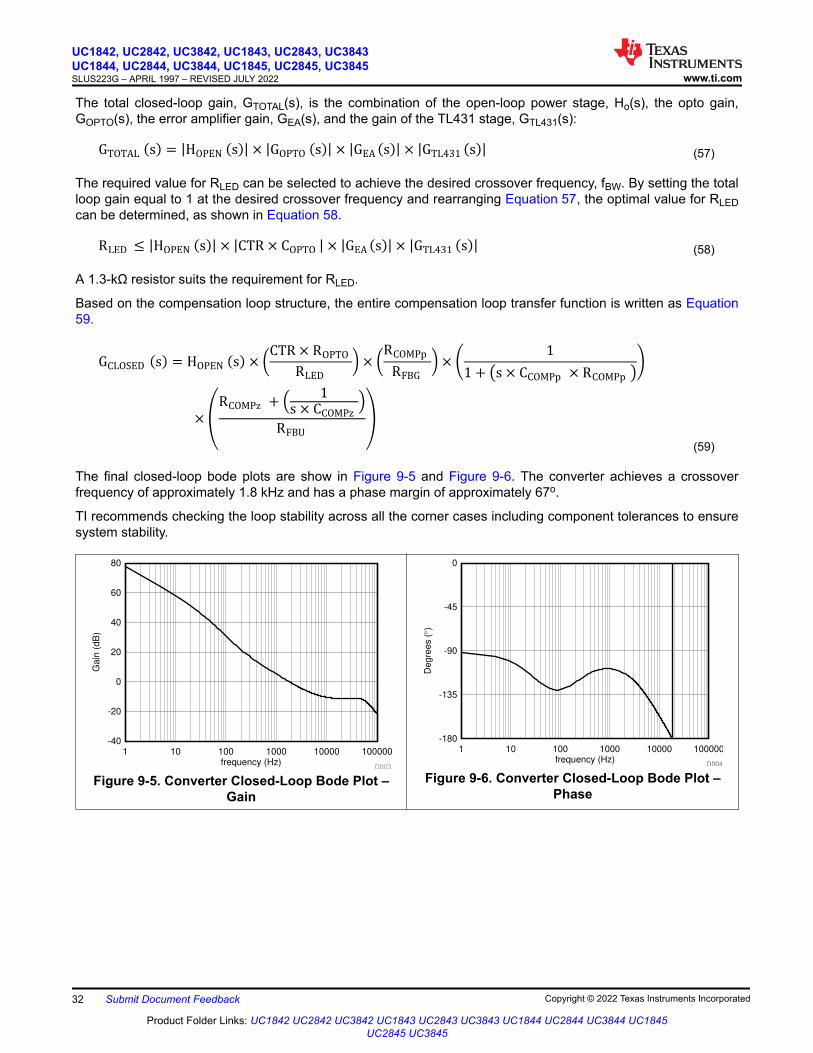
The total closed-loop gain, GTOTAL(s), is the combination of the open-loop power stage, Ho(s), the opto gain, GOPTO(s), the error amplifier gain, GEA(s), and the gain of the TL431 stage, GTL431(s):
GTOTAL :s; = HOPEN :s; × GOPTO :s; × GEA :s; × GTL431 :s; (57)
The required value for RLED can be selected to achieve the desired crossover frequency, fBW. By setting the total loop gain equal to 1 at the desired crossover frequency and rearranging Equation 57, the optimal value for RLED can be determined, as shown in Equation 58.
RLED Q HOPEN :s; × CTR × COPTO × GEA :s; × GTL431 :s; (58)
A 1.3-kΩ resistor suits the requirement for RLED.
Based on the compensation loop structure, the entire compensation loop transfer function is written as Equation 59.
GCLOSED :s; = HOPEN :s; × lCTR × ROPTORLED
p × lRCOMPpRFBG
p × F 1
1 + ks × CCOMPp × RCOMPp oG× nRCOMPz + @ 1
s × CCOMPzA
RFBUr
(59)
The final closed-loop bode plots are show in Figure 9-5 and Figure 9-6. The converter achieves a crossover frequency of approximately 1.8 kHz and has a phase margin of approximately 67o.
TI recommends checking the loop stability across all the corner cases including component tolerances to ensure system stability.
frequency (Hz)
Ga
in (
dB
)
1 10 100 1000 10000 100000-40
-20
0
20
40
60
80
D003
Figure 9-5. Converter Closed-Loop Bode Plot – Gain
frequency (Hz)
Deg
ree
s (q)
1 10 100 1000 10000 100000-180
-135
-90
-45
0
D001D004
Figure 9-6. Converter Closed-Loop Bode Plot – Phase
UC1842, UC2842, UC3842, UC1843, UC2843, UC3843UC1844, UC2844, UC3844, UC1845, UC2845, UC3845SLUS223G – APRIL 1997 – REVISED JULY 2022 www.ti.com
32 Submit Document Feedback Copyright © 2022 Texas Instruments Incorporated
Product Folder Links: UC1842 UC2842 UC3842 UC1843 UC2843 UC3843 UC1844 UC2844 UC3844 UC1845 UC2845 UC3845
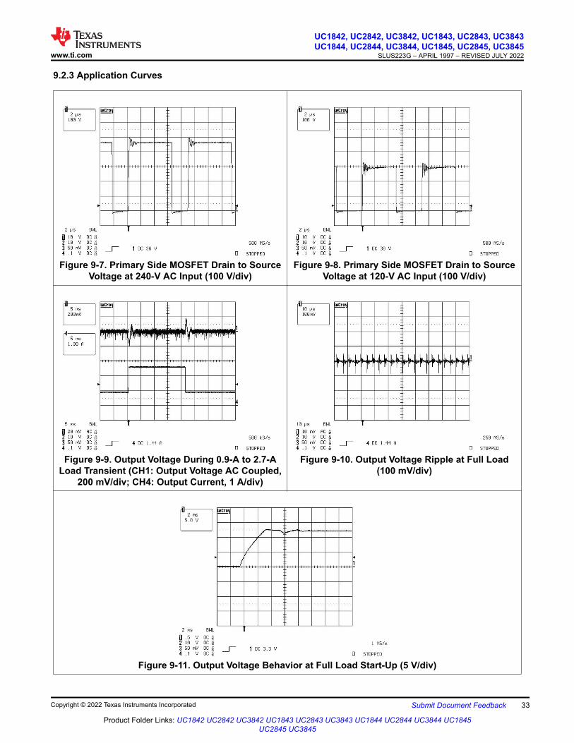
9.2.3 Application Curves
Figure 9-7. Primary Side MOSFET Drain to Source Voltage at 240-V AC Input (100 V/div)
Figure 9-8. Primary Side MOSFET Drain to Source Voltage at 120-V AC Input (100 V/div)
Figure 9-9. Output Voltage During 0.9-A to 2.7-A Load Transient (CH1: Output Voltage AC Coupled,
200 mV/div; CH4: Output Current, 1 A/div)
Figure 9-10. Output Voltage Ripple at Full Load (100 mV/div)
Figure 9-11. Output Voltage Behavior at Full Load Start-Up (5 V/div)
www.ti.com
UC1842, UC2842, UC3842, UC1843, UC2843, UC3843UC1844, UC2844, UC3844, UC1845, UC2845, UC3845
SLUS223G – APRIL 1997 – REVISED JULY 2022
Copyright © 2022 Texas Instruments Incorporated Submit Document Feedback 33
Product Folder Links: UC1842 UC2842 UC3842 UC1843 UC2843 UC3843 UC1844 UC2844 UC3844 UC1845 UC2845 UC3845
10 Power Supply RecommendationsIt is important to bypass the ICs supply (VCC) and reference voltage (VREF) pins with a 0.1-µF to 1-µF ceramic capacitor to ground. The capacitors must be placed as close to the actual pin connections as possible for optimal noise filtering. A second, larger filter capacitor may also be required in offline applications to hold the supply voltage (VCC) above the UVLO turnoff threshold during start-up.
To prevent false triggering due to leading edge noises, an RC current sense filter may be required on ISENSE. Keep the time constant of the RC filter well below the minimum on-time pulse width.
Schottky diodes may be necessary on the OUTPUT pin to prevent overshoot and undershoot due to the high impedance to the supply rail and to ground, respectively. A bleeder resistor, placed between the gate and the source of the MOSFET should be used to prevent activating the power switch with extraneous leakage currents during undervoltage lockout.
To prevent noise problems with high-speed switching transients, bypass VREF to ground with a ceramic capacitor close to the IC package. A minimum of 0.1-µF ceramic capacitor is required. Additional VREF bypassing is required for external loads on the reference. An electrolytic capacitor may also be used in addition to the ceramic capacitor.
UC1842, UC2842, UC3842, UC1843, UC2843, UC3843UC1844, UC2844, UC3844, UC1845, UC2845, UC3845SLUS223G – APRIL 1997 – REVISED JULY 2022 www.ti.com
34 Submit Document Feedback Copyright © 2022 Texas Instruments Incorporated
Product Folder Links: UC1842 UC2842 UC3842 UC1843 UC2843 UC3843 UC1844 UC2844 UC3844 UC1845 UC2845 UC3845

11 Layout11.1 Layout Guidelines11.1.1 Feedback Traces
Try to run the feedback trace as far from the inductor and noisy power traces as possible. Be as direct as possible with the feedback trace and somewhat thick. These two sometimes involve a trade-off, but keeping it away from EMI and other noise sources is the more critical of the two. If possible, run the feedback trace on the side of the PCB opposite of the inductor with a ground plane separating the two.
11.1.2 Bypass Capacitors
When using a low value ceramic bypass capacitor, it should be located as close to the VCC pin of the device as possible. This eliminates as much trace inductance effects as possible and gives the internal device rail a cleaner voltage supply. Using surface mount capacitors also reduces lead length and lessens the chance of noise coupling into the effective antenna created by through-hole components.
11.1.3 Compensation Components
For best stability, external compensation components should be placed close to the IC. Keep VFB lead length as short as possible and VFB stray capacitance as small as possible. Surface mount components are recommended here as well for the same reasons discussed for the filter capacitors. These should not be located very close to traces with high switching noise.
11.1.4 Traces and Ground Planes
Make all of the power (high current) traces as short, direct, and thick as possible. It is good practice on a standard PCB board to make the traces an absolute minimum of 15 mils (0.381 mm) per Ampere. The inductor, output capacitors, and output diode should be as close to each other possible. This helps reduce the EMI radiated by the power traces due to the high switching currents through them. This also reduces lead inductance and resistance as well, which in turn reduces noise spikes, ringing, and resistive losses that produce voltage errors.
The grounds of the IC, input capacitors, output capacitors, and output diode (if applicable) should be connected close together directly to a ground plane. It would also be a good idea to have a ground plane on both sides of the PCB. This reduces noise as well by reducing ground loop errors as well as by absorbing more of the EMI radiated by the inductor. For multi-layer boards with more than two layers, a ground plane can be used to separate the power plane (where the power traces and components are) and the signal plane (where the feedback and compensation and components are) for improved performance. On multi-layer boards the use of vias is required to connect traces and different planes. It is good practice to use one standard via per 200 mA of current if the trace needs to conduct a significant amount of current from one plane to the other.
Arrange the components so that the switching current loops curl in the same direction. Due to the way switching regulators operate, there are two power states. One state when the switch is on and one when the switch is off. During each state there is a current loop made by the power components that are currently conducting. Place the power components so that during each of the two states the current loop is conducting in the same direction. This prevents magnetic field reversal caused by the traces between the two half-cycles and reduces radiated EMI.
www.ti.com
UC1842, UC2842, UC3842, UC1843, UC2843, UC3843UC1844, UC2844, UC3844, UC1845, UC2845, UC3845
SLUS223G – APRIL 1997 – REVISED JULY 2022
Copyright © 2022 Texas Instruments Incorporated Submit Document Feedback 35
Product Folder Links: UC1842 UC2842 UC3842 UC1843 UC2843 UC3843 UC1844 UC2844 UC3844 UC1845 UC2845 UC3845
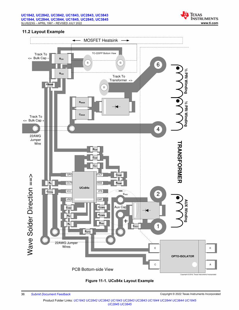
11.2 Layout Example
TO-220FP Bottom View
VREF
OUTPUT
COMP
ISENSE
VFB
RT/CT
VCC
GROUND
UCx84x
RP
ROPTO
RRT
CCT
CVREF
CCSF
CVCCbp
RRAMP
CRAMP
RG
RCSF
RCS1
RCS2
Track To
Transformer =>
FBead
CCOMPp
RCOMPp
RFBG
Track To
<= %XON&DSÅ
MOSFET Heatsink
Aux Cap
S
D
G
CSNUB
RSNUB
Wa
ve
So
lde
r D
ire
ctio
n =
=>
CVCC1
CVCC
Track To
<= Bulk Cap +
TR
AN
SF
OR
ME
R6
4
1
2
AU
X W
ind
ing
½ P
RI W
ind
ing
½ P
RI W
ind
ing
22AWG
Jumper
Wire
22AWG Jumper
Wires
PCB Bottom-side View
K
AC
E
OPTO-ISOLATOR
Copyright © 2016, Texas Instruments Incorporated
Figure 11-1. UCx84x Layout Example
UC1842, UC2842, UC3842, UC1843, UC2843, UC3843UC1844, UC2844, UC3844, UC1845, UC2845, UC3845SLUS223G – APRIL 1997 – REVISED JULY 2022 www.ti.com
36 Submit Document Feedback Copyright © 2022 Texas Instruments Incorporated
Product Folder Links: UC1842 UC2842 UC3842 UC1843 UC2843 UC3843 UC1844 UC2844 UC3844 UC1845 UC2845 UC3845

12 Device and Documentation Support12.1 Receiving Notification of Documentation UpdatesTo receive notification of documentation updates, navigate to the device product folder on ti.com. Click on Subscribe to updates to register and receive a weekly digest of any product information that has changed. For change details, review the revision history included in any revised document.
12.2 Support ResourcesTI E2E™ support forums are an engineer's go-to source for fast, verified answers and design help — straight from the experts. Search existing answers or ask your own question to get the quick design help you need.
Linked content is provided "AS IS" by the respective contributors. They do not constitute TI specifications and do not necessarily reflect TI's views; see TI's Terms of Use.
12.3 TrademarksTI E2E™ is a trademark of Texas Instruments.All trademarks are the property of their respective owners.12.4 Electrostatic Discharge Caution
This integrated circuit can be damaged by ESD. Texas Instruments recommends that all integrated circuits be handled with appropriate precautions. Failure to observe proper handling and installation procedures can cause damage.ESD damage can range from subtle performance degradation to complete device failure. Precision integrated circuits may be more susceptible to damage because very small parametric changes could cause the device not to meet its published specifications.
12.5 GlossaryTI Glossary This glossary lists and explains terms, acronyms, and definitions.
13 Mechanical, Packaging, and Orderable InformationThe following pages include mechanical, packaging, and orderable information. This information is the most current data available for the designated devices. This data is subject to change without notice and revision of this document. For browser-based versions of this data sheet, see the left-hand navigation.
www.ti.com
UC1842, UC2842, UC3842, UC1843, UC2843, UC3843UC1844, UC2844, UC3844, UC1845, UC2845, UC3845
SLUS223G – APRIL 1997 – REVISED JULY 2022
Copyright © 2022 Texas Instruments Incorporated Submit Document Feedback 37
Product Folder Links: UC1842 UC2842 UC3842 UC1843 UC2843 UC3843 UC1844 UC2844 UC3844 UC1845 UC2845 UC3845

PACKAGE OPTION ADDENDUM
www.ti.com 13-Jul-2022
PACKAGING INFORMATION
Orderable Device Status(1)
Package Type PackageDrawing
Pins PackageQty
Eco Plan(2)
Lead finish/Ball material
(6)
MSL Peak Temp(3)
Op Temp (°C) Device Marking(4/5)
Samples
5962-8670401PA ACTIVE CDIP JG 8 1 Non-RoHS& Green
SNPB N / A for Pkg Type -55 to 125 8670401PAUC1842
Samples
5962-8670401VPA ACTIVE CDIP JG 8 1 Non-RoHS& Green
SNPB N / A for Pkg Type -55 to 125 8670401VPAUC1842
Samples
5962-8670401XA ACTIVE LCCC FK 20 1 Non-RoHS& Green
SNPB N / A for Pkg Type -55 to 125 5962-8670401XAUC1842L/883B
Samples
5962-8670402PA ACTIVE CDIP JG 8 1 Non-RoHS& Green
SNPB N / A for Pkg Type -55 to 125 8670402PAUC1843
Samples
5962-8670402XA ACTIVE LCCC FK 20 1 Non-RoHS& Green
SNPB N / A for Pkg Type -55 to 125 5962-8670402XAUC1843L/883B
Samples
5962-8670403PA ACTIVE CDIP JG 8 1 Non-RoHS& Green
SNPB N / A for Pkg Type -55 to 125 8670403PAUC1844
Samples
5962-8670403VXA ACTIVE LCCC FK 20 1 Non-RoHS& Green
SNPB N / A for Pkg Type -55 to 125 5962-8670403VXAUC1844LQMLV
Samples
5962-8670403XA ACTIVE LCCC FK 20 1 Non-RoHS& Green
SNPB N / A for Pkg Type -55 to 125 5962-8670403XAUC1844L/883B
Samples
5962-8670404DA ACTIVE CFP W 14 1 Non-RoHS& Green
SNPB N / A for Pkg Type 5962-8670404DAUC1845W/883B
Samples
5962-8670404PA ACTIVE CDIP JG 8 1 Non-RoHS& Green
SNPB N / A for Pkg Type -55 to 125 8670404PAUC1845
Samples
5962-8670404VPA ACTIVE CDIP JG 8 1 Non-RoHS& Green
SNPB N / A for Pkg Type 8670404VPAUC1845
Samples
5962-8670404VXA ACTIVE LCCC FK 20 1 Non-RoHS& Green
SNPB N / A for Pkg Type -55 to 125 5962-8670404VXAUC1845LQMLV
Samples
Addendum-Page 1

PACKAGE OPTION ADDENDUM
www.ti.com 13-Jul-2022
Orderable Device Status(1)
Package Type PackageDrawing
Pins PackageQty
Eco Plan(2)
Lead finish/Ball material
(6)
MSL Peak Temp(3)
Op Temp (°C) Device Marking(4/5)
Samples
5962-8670404XA ACTIVE LCCC FK 20 1 Non-RoHS& Green
SNPB N / A for Pkg Type -55 to 125 5962-8670404XAUC1845L/883B
Samples
UC1842J ACTIVE CDIP JG 8 1 Non-RoHS& Green
SNPB N / A for Pkg Type -55 to 125 UC1842J Samples
UC1842J883B ACTIVE CDIP JG 8 1 Non-RoHS& Green
SNPB N / A for Pkg Type -55 to 125 8670401PAUC1842
Samples
UC1842L883B ACTIVE LCCC FK 20 1 Non-RoHS& Green
SNPB N / A for Pkg Type -55 to 125 5962-8670401XAUC1842L/883B
Samples
UC1842W ACTIVE CFP W 14 1 Non-RoHS& Green
SNPB N / A for Pkg Type -55 to 125 UC1842W Samples
UC1843J ACTIVE CDIP JG 8 50 Non-RoHS& Green
SNPB N / A for Pkg Type -55 to 125 UC1843J Samples
UC1843J883B ACTIVE CDIP JG 8 1 Non-RoHS& Green
SNPB N / A for Pkg Type -55 to 125 8670402PAUC1843
Samples
UC1843L ACTIVE LCCC FK 20 1 Non-RoHS& Green
SNPB N / A for Pkg Type -55 to 125 UC1843L Samples
UC1843L883B ACTIVE LCCC FK 20 1 Non-RoHS& Green
SNPB N / A for Pkg Type -55 to 125 5962-8670402XAUC1843L/883B
Samples
UC1844J ACTIVE CDIP JG 8 1 Non-RoHS& Green
SNPB N / A for Pkg Type -55 to 125 UC1844J Samples
UC1844J883B ACTIVE CDIP JG 8 1 Non-RoHS& Green
SNPB N / A for Pkg Type -55 to 125 8670403PAUC1844
Samples
UC1844L883B ACTIVE LCCC FK 20 1 Non-RoHS& Green
SNPB N / A for Pkg Type -55 to 125 5962-8670403XAUC1844L/883B
Samples
UC1845J ACTIVE CDIP JG 8 1 Non-RoHS& Green
SNPB N / A for Pkg Type -55 to 125 UC1845J Samples
UC1845J883B ACTIVE CDIP JG 8 1 Non-RoHS& Green
SNPB N / A for Pkg Type -55 to 125 8670404PAUC1845
Samples
Addendum-Page 2
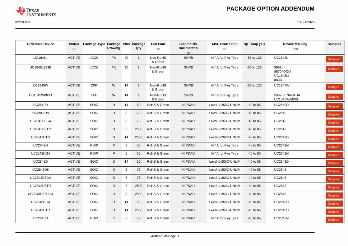
PACKAGE OPTION ADDENDUM
www.ti.com 13-Jul-2022
Orderable Device Status(1)
Package Type PackageDrawing
Pins PackageQty
Eco Plan(2)
Lead finish/Ball material
(6)
MSL Peak Temp(3)
Op Temp (°C) Device Marking(4/5)
Samples
UC1845L ACTIVE LCCC FK 20 1 Non-RoHS& Green
SNPB N / A for Pkg Type -55 to 125 UC1845L Samples
UC1845L883B ACTIVE LCCC FK 20 1 Non-RoHS& Green
SNPB N / A for Pkg Type -55 to 125 5962-8670404XAUC1845L/883B
Samples
UC1845W ACTIVE CFP W 14 1 Non-RoHS& Green
SNPB N / A for Pkg Type -55 to 125 UC1845W Samples
UC1845W883B ACTIVE CFP W 14 1 Non-RoHS& Green
SNPB N / A for Pkg Type 5962-8670404DAUC1845W/883B
Samples
UC2842D ACTIVE SOIC D 14 50 RoHS & Green NIPDAU Level-1-260C-UNLIM -40 to 85 UC2842D Samples
UC2842D8 ACTIVE SOIC D 8 75 RoHS & Green NIPDAU Level-1-260C-UNLIM -40 to 85 UC2842 Samples
UC2842D8G4 ACTIVE SOIC D 8 75 RoHS & Green NIPDAU Level-1-260C-UNLIM -40 to 85 UC2842 Samples
UC2842D8TR ACTIVE SOIC D 8 2500 RoHS & Green NIPDAU Level-1-260C-UNLIM -40 to 85 UC2842 Samples
UC2842DTR ACTIVE SOIC D 14 2500 RoHS & Green NIPDAU Level-1-260C-UNLIM -40 to 85 UC2842D Samples
UC2842N ACTIVE PDIP P 8 50 RoHS & Green NIPDAU N / A for Pkg Type -40 to 85 UC2842N Samples
UC2842NG4 ACTIVE PDIP P 8 50 RoHS & Green NIPDAU N / A for Pkg Type -40 to 85 UC2842N Samples
UC2843D ACTIVE SOIC D 14 50 RoHS & Green NIPDAU Level-1-260C-UNLIM -40 to 85 UC2843D Samples
UC2843D8 ACTIVE SOIC D 8 75 RoHS & Green NIPDAU Level-1-260C-UNLIM -40 to 85 UC2843 Samples
UC2843D8G4 ACTIVE SOIC D 8 75 RoHS & Green NIPDAU Level-1-260C-UNLIM -40 to 85 UC2843 Samples
UC2843D8TR ACTIVE SOIC D 8 2500 RoHS & Green NIPDAU Level-1-260C-UNLIM -40 to 85 UC2843 Samples
UC2843D8TRG4 ACTIVE SOIC D 8 2500 RoHS & Green NIPDAU Level-1-260C-UNLIM -40 to 85 UC2843 Samples
UC2843DG4 ACTIVE SOIC D 14 50 RoHS & Green NIPDAU Level-1-260C-UNLIM -40 to 85 UC2843D Samples
UC2843DTR ACTIVE SOIC D 14 2500 RoHS & Green NIPDAU Level-1-260C-UNLIM -40 to 85 UC2843D Samples
UC2843N ACTIVE PDIP P 8 50 RoHS & Green NIPDAU N / A for Pkg Type -40 to 85 UC2843N Samples
Addendum-Page 3
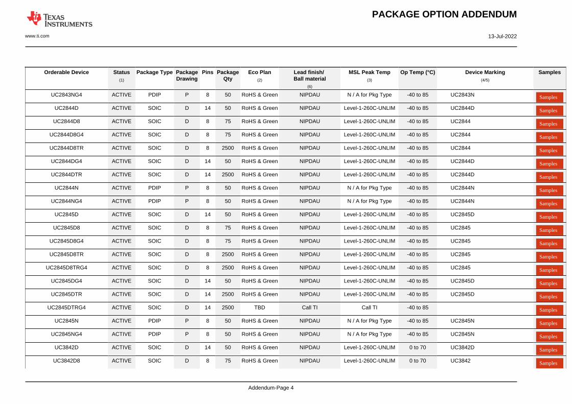
PACKAGE OPTION ADDENDUM
www.ti.com 13-Jul-2022
Orderable Device Status(1)
Package Type PackageDrawing
Pins PackageQty
Eco Plan(2)
Lead finish/Ball material
(6)
MSL Peak Temp(3)
Op Temp (°C) Device Marking(4/5)
Samples
UC2843NG4 ACTIVE PDIP P 8 50 RoHS & Green NIPDAU N / A for Pkg Type -40 to 85 UC2843N Samples
UC2844D ACTIVE SOIC D 14 50 RoHS & Green NIPDAU Level-1-260C-UNLIM -40 to 85 UC2844D Samples
UC2844D8 ACTIVE SOIC D 8 75 RoHS & Green NIPDAU Level-1-260C-UNLIM -40 to 85 UC2844 Samples
UC2844D8G4 ACTIVE SOIC D 8 75 RoHS & Green NIPDAU Level-1-260C-UNLIM -40 to 85 UC2844 Samples
UC2844D8TR ACTIVE SOIC D 8 2500 RoHS & Green NIPDAU Level-1-260C-UNLIM -40 to 85 UC2844 Samples
UC2844DG4 ACTIVE SOIC D 14 50 RoHS & Green NIPDAU Level-1-260C-UNLIM -40 to 85 UC2844D Samples
UC2844DTR ACTIVE SOIC D 14 2500 RoHS & Green NIPDAU Level-1-260C-UNLIM -40 to 85 UC2844D Samples
UC2844N ACTIVE PDIP P 8 50 RoHS & Green NIPDAU N / A for Pkg Type -40 to 85 UC2844N Samples
UC2844NG4 ACTIVE PDIP P 8 50 RoHS & Green NIPDAU N / A for Pkg Type -40 to 85 UC2844N Samples
UC2845D ACTIVE SOIC D 14 50 RoHS & Green NIPDAU Level-1-260C-UNLIM -40 to 85 UC2845D Samples
UC2845D8 ACTIVE SOIC D 8 75 RoHS & Green NIPDAU Level-1-260C-UNLIM -40 to 85 UC2845 Samples
UC2845D8G4 ACTIVE SOIC D 8 75 RoHS & Green NIPDAU Level-1-260C-UNLIM -40 to 85 UC2845 Samples
UC2845D8TR ACTIVE SOIC D 8 2500 RoHS & Green NIPDAU Level-1-260C-UNLIM -40 to 85 UC2845 Samples
UC2845D8TRG4 ACTIVE SOIC D 8 2500 RoHS & Green NIPDAU Level-1-260C-UNLIM -40 to 85 UC2845 Samples
UC2845DG4 ACTIVE SOIC D 14 50 RoHS & Green NIPDAU Level-1-260C-UNLIM -40 to 85 UC2845D Samples
UC2845DTR ACTIVE SOIC D 14 2500 RoHS & Green NIPDAU Level-1-260C-UNLIM -40 to 85 UC2845D Samples
UC2845DTRG4 ACTIVE SOIC D 14 2500 TBD Call TI Call TI -40 to 85 Samples
UC2845N ACTIVE PDIP P 8 50 RoHS & Green NIPDAU N / A for Pkg Type -40 to 85 UC2845N Samples
UC2845NG4 ACTIVE PDIP P 8 50 RoHS & Green NIPDAU N / A for Pkg Type -40 to 85 UC2845N Samples
UC3842D ACTIVE SOIC D 14 50 RoHS & Green NIPDAU Level-1-260C-UNLIM 0 to 70 UC3842D Samples
UC3842D8 ACTIVE SOIC D 8 75 RoHS & Green NIPDAU Level-1-260C-UNLIM 0 to 70 UC3842 Samples
Addendum-Page 4

PACKAGE OPTION ADDENDUM
www.ti.com 13-Jul-2022
Orderable Device Status(1)
Package Type PackageDrawing
Pins PackageQty
Eco Plan(2)
Lead finish/Ball material
(6)
MSL Peak Temp(3)
Op Temp (°C) Device Marking(4/5)
Samples
UC3842D8TR ACTIVE SOIC D 8 2500 RoHS & Green NIPDAU Level-1-260C-UNLIM 0 to 70 UC3842 Samples
UC3842DTR ACTIVE SOIC D 14 2500 RoHS & Green NIPDAU Level-1-260C-UNLIM 0 to 70 UC3842D Samples
UC3842N ACTIVE PDIP P 8 50 RoHS & Green NIPDAU N / A for Pkg Type 0 to 70 UC3842N Samples
UC3842NG4 ACTIVE PDIP P 8 50 RoHS & Green NIPDAU N / A for Pkg Type 0 to 70 UC3842N Samples
UC3843D ACTIVE SOIC D 14 50 RoHS & Green NIPDAU Level-1-260C-UNLIM 0 to 70 UC3843D Samples
UC3843D8 ACTIVE SOIC D 8 75 RoHS & Green NIPDAU Level-1-260C-UNLIM 0 to 70 UC3843 Samples
UC3843D8G4 ACTIVE SOIC D 8 75 RoHS & Green NIPDAU Level-1-260C-UNLIM 0 to 70 UC3843 Samples
UC3843D8TR ACTIVE SOIC D 8 2500 RoHS & Green NIPDAU Level-1-260C-UNLIM 0 to 70 UC3843 Samples
UC3843D8TRG4 ACTIVE SOIC D 8 2500 RoHS & Green NIPDAU Level-1-260C-UNLIM 0 to 70 UC3843 Samples
UC3843DG4 ACTIVE SOIC D 14 50 RoHS & Green NIPDAU Level-1-260C-UNLIM 0 to 70 UC3843D Samples
UC3843DTR ACTIVE SOIC D 14 2500 RoHS & Green NIPDAU Level-1-260C-UNLIM 0 to 70 UC3843D Samples
UC3843N ACTIVE PDIP P 8 50 RoHS & Green NIPDAU N / A for Pkg Type 0 to 70 UC3843N Samples
UC3843NG4 ACTIVE PDIP P 8 50 RoHS & Green NIPDAU N / A for Pkg Type 0 to 70 UC3843N Samples
UC3844D ACTIVE SOIC D 14 50 RoHS & Green NIPDAU Level-1-260C-UNLIM 0 to 70 UC3844D Samples
UC3844D8 ACTIVE SOIC D 8 75 RoHS & Green NIPDAU Level-1-260C-UNLIM 0 to 70 UC3844 Samples
UC3844D8TR ACTIVE SOIC D 8 2500 RoHS & Green NIPDAU Level-1-260C-UNLIM 0 to 70 UC3844 Samples
UC3844D8TRG4 ACTIVE SOIC D 8 2500 TBD Call TI Call TI 0 to 70 Samples
UC3844DTR ACTIVE SOIC D 14 2500 RoHS & Green NIPDAU Level-1-260C-UNLIM 0 to 70 UC3844D Samples
UC3844DTRG4 ACTIVE SOIC D 14 2500 RoHS & Green NIPDAU Level-1-260C-UNLIM 0 to 70 UC3844D Samples
UC3844N ACTIVE PDIP P 8 50 RoHS & Green NIPDAU N / A for Pkg Type 0 to 70 UC3844N Samples
UC3844NG4 ACTIVE PDIP P 8 50 RoHS & Green NIPDAU N / A for Pkg Type 0 to 70 UC3844N Samples
Addendum-Page 5

PACKAGE OPTION ADDENDUM
www.ti.com 13-Jul-2022
Orderable Device Status(1)
Package Type PackageDrawing
Pins PackageQty
Eco Plan(2)
Lead finish/Ball material
(6)
MSL Peak Temp(3)
Op Temp (°C) Device Marking(4/5)
Samples
UC3845AJ ACTIVE CDIP JG 8 1 Non-RoHS& Green
SNPB N / A for Pkg Type 0 to 70 UC3845AJ Samples
UC3845D ACTIVE SOIC D 14 50 RoHS & Green NIPDAU Level-1-260C-UNLIM 0 to 70 UC3845D Samples
UC3845D8 ACTIVE SOIC D 8 75 RoHS & Green NIPDAU Level-1-260C-UNLIM 0 to 70 UC3845 Samples
UC3845D8G4 ACTIVE SOIC D 8 75 RoHS & Green NIPDAU Level-1-260C-UNLIM 0 to 70 UC3845 Samples
UC3845D8TR ACTIVE SOIC D 8 2500 RoHS & Green NIPDAU Level-1-260C-UNLIM 0 to 70 UC3845 Samples
UC3845D8TRG4 ACTIVE SOIC D 8 2500 RoHS & Green NIPDAU Level-1-260C-UNLIM 0 to 70 UC3845 Samples
UC3845DG4 ACTIVE SOIC D 14 50 RoHS & Green NIPDAU Level-1-260C-UNLIM 0 to 70 UC3845D Samples
UC3845DTR ACTIVE SOIC D 14 2500 RoHS & Green NIPDAU Level-1-260C-UNLIM 0 to 70 UC3845D Samples
UC3845N ACTIVE PDIP P 8 50 RoHS & Green NIPDAU N / A for Pkg Type 0 to 70 UC3845N Samples
UC3845NG4 ACTIVE PDIP P 8 50 RoHS & Green NIPDAU N / A for Pkg Type 0 to 70 UC3845N Samples
(1) The marketing status values are defined as follows:ACTIVE: Product device recommended for new designs.LIFEBUY: TI has announced that the device will be discontinued, and a lifetime-buy period is in effect.NRND: Not recommended for new designs. Device is in production to support existing customers, but TI does not recommend using this part in a new design.PREVIEW: Device has been announced but is not in production. Samples may or may not be available.OBSOLETE: TI has discontinued the production of the device.
(2) RoHS: TI defines "RoHS" to mean semiconductor products that are compliant with the current EU RoHS requirements for all 10 RoHS substances, including the requirement that RoHS substancedo not exceed 0.1% by weight in homogeneous materials. Where designed to be soldered at high temperatures, "RoHS" products are suitable for use in specified lead-free processes. TI mayreference these types of products as "Pb-Free".RoHS Exempt: TI defines "RoHS Exempt" to mean products that contain lead but are compliant with EU RoHS pursuant to a specific EU RoHS exemption.Green: TI defines "Green" to mean the content of Chlorine (Cl) and Bromine (Br) based flame retardants meet JS709B low halogen requirements of <=1000ppm threshold. Antimony trioxide basedflame retardants must also meet the <=1000ppm threshold requirement.
(3) MSL, Peak Temp. - The Moisture Sensitivity Level rating according to the JEDEC industry standard classifications, and peak solder temperature.
(4) There may be additional marking, which relates to the logo, the lot trace code information, or the environmental category on the device.
Addendum-Page 6

PACKAGE OPTION ADDENDUM
www.ti.com 13-Jul-2022
(5) Multiple Device Markings will be inside parentheses. Only one Device Marking contained in parentheses and separated by a "~" will appear on a device. If a line is indented then it is a continuationof the previous line and the two combined represent the entire Device Marking for that device.
(6) Lead finish/Ball material - Orderable Devices may have multiple material finish options. Finish options are separated by a vertical ruled line. Lead finish/Ball material values may wrap to twolines if the finish value exceeds the maximum column width.
Important Information and Disclaimer:The information provided on this page represents TI's knowledge and belief as of the date that it is provided. TI bases its knowledge and belief on informationprovided by third parties, and makes no representation or warranty as to the accuracy of such information. Efforts are underway to better integrate information from third parties. TI has taken andcontinues to take reasonable steps to provide representative and accurate information but may not have conducted destructive testing or chemical analysis on incoming materials and chemicals.TI and TI suppliers consider certain information to be proprietary, and thus CAS numbers and other limited information may not be available for release.
In no event shall TI's liability arising out of such information exceed the total purchase price of the TI part(s) at issue in this document sold by TI to Customer on an annual basis.
OTHER QUALIFIED VERSIONS OF UC1842, UC1842-SP, UC1843, UC1844, UC1844-SP, UC1845, UC1845-SP, UC3842, UC3843, UC3844, UC3845, UC3845AM :
• Catalog : UC3842, UC1842, UC3843, UC3844, UC1844, UC3845, UC1845, UC3842M, UC3845A
• Enhanced Product : UC1845A-EP
• Military : UC1842, UC1843, UC1844, UC1845, UC1845A
• Space : UC1842-SP, UC1843-SP, UC1844-SP, UC1845-SP, UC1845A-SP
NOTE: Qualified Version Definitions:
• Catalog - TI's standard catalog product
• Enhanced Product - Supports Defense, Aerospace and Medical Applications
• Military - QML certified for Military and Defense Applications
• Space - Radiation tolerant, ceramic packaging and qualified for use in Space-based application
Addendum-Page 7

PACKAGE MATERIALS INFORMATION
www.ti.com 4-May-2022
TAPE AND REEL INFORMATION
Reel Width (W1)
REEL DIMENSIONS
A0B0K0W
Dimension designed to accommodate the component lengthDimension designed to accommodate the component thicknessOverall width of the carrier tapePitch between successive cavity centers
Dimension designed to accommodate the component width
TAPE DIMENSIONS
K0 P1
B0 W
A0Cavity
QUADRANT ASSIGNMENTS FOR PIN 1 ORIENTATION IN TAPE
Pocket Quadrants
Sprocket Holes
Q1 Q1Q2 Q2
Q3 Q3Q4 Q4 User Direction of Feed
P1
ReelDiameter
*All dimensions are nominal
Device PackageType
PackageDrawing
Pins SPQ ReelDiameter
(mm)
ReelWidth
W1 (mm)
A0(mm)
B0(mm)
K0(mm)
P1(mm)
W(mm)
Pin1Quadrant
UC2842D8TR SOIC D 8 2500 330.0 12.4 6.4 5.2 2.1 8.0 12.0 Q1
UC2842DTR SOIC D 14 2500 330.0 16.4 6.5 9.0 2.1 8.0 16.0 Q1
UC2843D8TR SOIC D 8 2500 330.0 12.4 6.4 5.2 2.1 8.0 12.0 Q1
UC2843DTR SOIC D 14 2500 330.0 16.4 6.5 9.0 2.1 8.0 16.0 Q1
UC2844D8TR SOIC D 8 2500 330.0 12.4 6.4 5.2 2.1 8.0 12.0 Q1
UC2844DTR SOIC D 14 2500 330.0 16.4 6.5 9.0 2.1 8.0 16.0 Q1
UC2845D8TR SOIC D 8 2500 330.0 12.4 6.4 5.2 2.1 8.0 12.0 Q1
UC2845DTR SOIC D 14 2500 330.0 16.4 6.5 9.0 2.1 8.0 16.0 Q1
UC3842D8TR SOIC D 8 2500 330.0 12.4 6.4 5.2 2.1 8.0 12.0 Q1
UC3842DTR SOIC D 14 2500 330.0 16.4 6.5 9.0 2.1 8.0 16.0 Q1
UC3843D8TR SOIC D 8 2500 330.0 12.4 6.4 5.2 2.1 8.0 12.0 Q1
UC3843DTR SOIC D 14 2500 330.0 16.4 6.5 9.0 2.1 8.0 16.0 Q1
UC3844D8TR SOIC D 8 2500 330.0 12.4 6.4 5.2 2.1 8.0 12.0 Q1
UC3844DTR SOIC D 14 2500 330.0 16.4 6.5 9.0 2.1 8.0 16.0 Q1
UC3845D8TR SOIC D 8 2500 330.0 12.4 6.4 5.2 2.1 8.0 12.0 Q1
UC3845DTR SOIC D 14 2500 330.0 16.4 6.5 9.0 2.1 8.0 16.0 Q1
Pack Materials-Page 1

PACKAGE MATERIALS INFORMATION
www.ti.com 4-May-2022
TAPE AND REEL BOX DIMENSIONS
Width (mm)
W L
H
*All dimensions are nominal
Device Package Type Package Drawing Pins SPQ Length (mm) Width (mm) Height (mm)
UC2842D8TR SOIC D 8 2500 340.5 336.1 25.0
UC2842DTR SOIC D 14 2500 340.5 336.1 32.0
UC2843D8TR SOIC D 8 2500 340.5 336.1 25.0
UC2843DTR SOIC D 14 2500 340.5 336.1 32.0
UC2844D8TR SOIC D 8 2500 340.5 336.1 25.0
UC2844DTR SOIC D 14 2500 340.5 336.1 32.0
UC2845D8TR SOIC D 8 2500 340.5 336.1 25.0
UC2845DTR SOIC D 14 2500 340.5 336.1 32.0
UC3842D8TR SOIC D 8 2500 340.5 336.1 25.0
UC3842DTR SOIC D 14 2500 340.5 336.1 32.0
UC3843D8TR SOIC D 8 2500 340.5 336.1 25.0
UC3843DTR SOIC D 14 2500 340.5 336.1 32.0
UC3844D8TR SOIC D 8 2500 340.5 336.1 25.0
UC3844DTR SOIC D 14 2500 340.5 336.1 32.0
UC3845D8TR SOIC D 8 2500 340.5 336.1 25.0
UC3845DTR SOIC D 14 2500 340.5 336.1 32.0
Pack Materials-Page 2
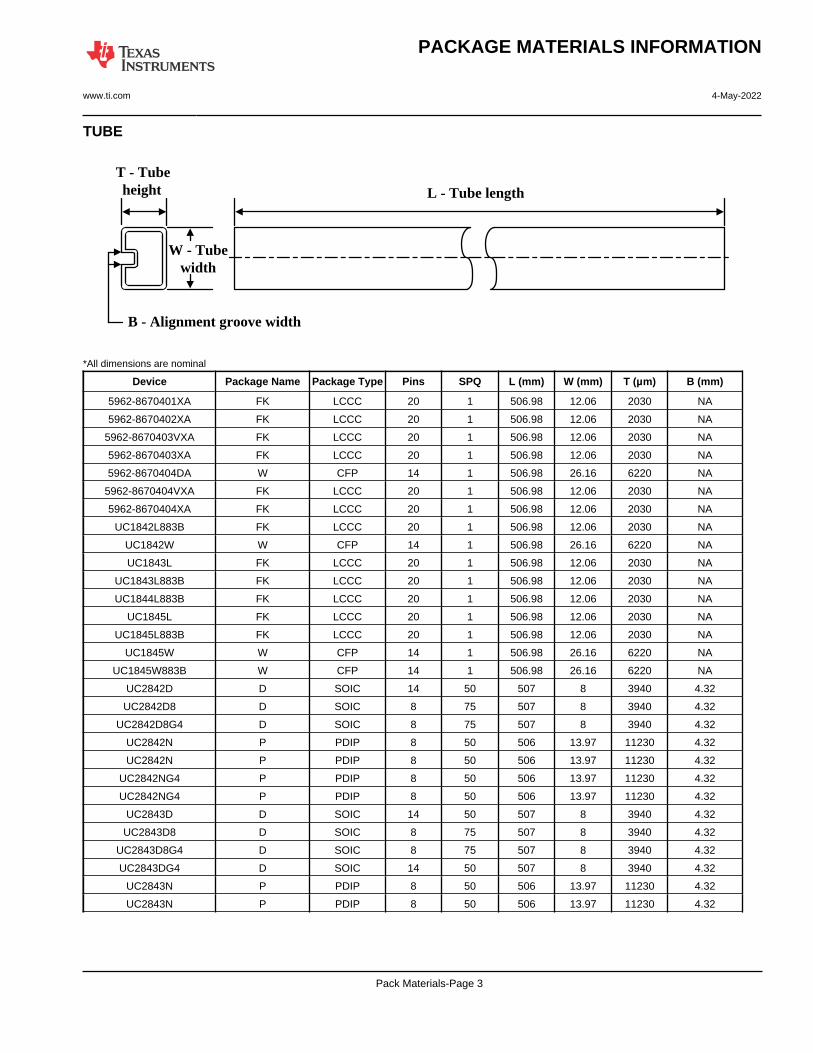
PACKAGE MATERIALS INFORMATION
www.ti.com 4-May-2022
TUBE
L - Tube lengthT - Tube height
W - Tube width
B - Alignment groove width *All dimensions are nominal
Device Package Name Package Type Pins SPQ L (mm) W (mm) T (µm) B (mm)
5962-8670401XA FK LCCC 20 1 506.98 12.06 2030 NA
5962-8670402XA FK LCCC 20 1 506.98 12.06 2030 NA
5962-8670403VXA FK LCCC 20 1 506.98 12.06 2030 NA
5962-8670403XA FK LCCC 20 1 506.98 12.06 2030 NA
5962-8670404DA W CFP 14 1 506.98 26.16 6220 NA
5962-8670404VXA FK LCCC 20 1 506.98 12.06 2030 NA
5962-8670404XA FK LCCC 20 1 506.98 12.06 2030 NA
UC1842L883B FK LCCC 20 1 506.98 12.06 2030 NA
UC1842W W CFP 14 1 506.98 26.16 6220 NA
UC1843L FK LCCC 20 1 506.98 12.06 2030 NA
UC1843L883B FK LCCC 20 1 506.98 12.06 2030 NA
UC1844L883B FK LCCC 20 1 506.98 12.06 2030 NA
UC1845L FK LCCC 20 1 506.98 12.06 2030 NA
UC1845L883B FK LCCC 20 1 506.98 12.06 2030 NA
UC1845W W CFP 14 1 506.98 26.16 6220 NA
UC1845W883B W CFP 14 1 506.98 26.16 6220 NA
UC2842D D SOIC 14 50 507 8 3940 4.32
UC2842D8 D SOIC 8 75 507 8 3940 4.32
UC2842D8G4 D SOIC 8 75 507 8 3940 4.32
UC2842N P PDIP 8 50 506 13.97 11230 4.32
UC2842N P PDIP 8 50 506 13.97 11230 4.32
UC2842NG4 P PDIP 8 50 506 13.97 11230 4.32
UC2842NG4 P PDIP 8 50 506 13.97 11230 4.32
UC2843D D SOIC 14 50 507 8 3940 4.32
UC2843D8 D SOIC 8 75 507 8 3940 4.32
UC2843D8G4 D SOIC 8 75 507 8 3940 4.32
UC2843DG4 D SOIC 14 50 507 8 3940 4.32
UC2843N P PDIP 8 50 506 13.97 11230 4.32
UC2843N P PDIP 8 50 506 13.97 11230 4.32
Pack Materials-Page 3

PACKAGE MATERIALS INFORMATION
www.ti.com 4-May-2022
Device Package Name Package Type Pins SPQ L (mm) W (mm) T (µm) B (mm)
UC2843NG4 P PDIP 8 50 506 13.97 11230 4.32
UC2843NG4 P PDIP 8 50 506 13.97 11230 4.32
UC2844D D SOIC 14 50 507 8 3940 4.32
UC2844D8 D SOIC 8 75 507 8 3940 4.32
UC2844D8G4 D SOIC 8 75 507 8 3940 4.32
UC2844DG4 D SOIC 14 50 507 8 3940 4.32
UC2844N P PDIP 8 50 506 13.97 11230 4.32
UC2844N P PDIP 8 50 506 13.97 11230 4.32
UC2844NG4 P PDIP 8 50 506 13.97 11230 4.32
UC2844NG4 P PDIP 8 50 506 13.97 11230 4.32
UC2845D D SOIC 14 50 507 8 3940 4.32
UC2845D8 D SOIC 8 75 507 8 3940 4.32
UC2845D8G4 D SOIC 8 75 507 8 3940 4.32
UC2845DG4 D SOIC 14 50 507 8 3940 4.32
UC2845N P PDIP 8 50 506 13.97 11230 4.32
UC2845N P PDIP 8 50 506 13.97 11230 4.32
UC2845NG4 P PDIP 8 50 506 13.97 11230 4.32
UC2845NG4 P PDIP 8 50 506 13.97 11230 4.32
UC3842D D SOIC 14 50 507 8 3940 4.32
UC3842D8 D SOIC 8 75 507 8 3940 4.32
UC3842N P PDIP 8 50 506 13.97 11230 4.32
UC3842N P PDIP 8 50 506 13.97 11230 4.32
UC3842NG4 P PDIP 8 50 506 13.97 11230 4.32
UC3842NG4 P PDIP 8 50 506 13.97 11230 4.32
UC3843D D SOIC 14 50 507 8 3940 4.32
UC3843D8 D SOIC 8 75 507 8 3940 4.32
UC3843D8G4 D SOIC 8 75 507 8 3940 4.32
UC3843DG4 D SOIC 14 50 507 8 3940 4.32
UC3843N P PDIP 8 50 506 13.97 11230 4.32
UC3843N P PDIP 8 50 506 13.97 11230 4.32
UC3843NG4 P PDIP 8 50 506 13.97 11230 4.32
UC3843NG4 P PDIP 8 50 506 13.97 11230 4.32
UC3844D D SOIC 14 50 507 8 3940 4.32
UC3844D8 D SOIC 8 75 507 8 3940 4.32
UC3844N P PDIP 8 50 506 13.97 11230 4.32
UC3844N P PDIP 8 50 506 13.97 11230 4.32
UC3844NG4 P PDIP 8 50 506 13.97 11230 4.32
UC3844NG4 P PDIP 8 50 506 13.97 11230 4.32
UC3845D D SOIC 14 50 507 8 3940 4.32
UC3845D8 D SOIC 8 75 507 8 3940 4.32
UC3845D8G4 D SOIC 8 75 507 8 3940 4.32
UC3845DG4 D SOIC 14 50 507 8 3940 4.32
UC3845N P PDIP 8 50 506 13.97 11230 4.32
Pack Materials-Page 4
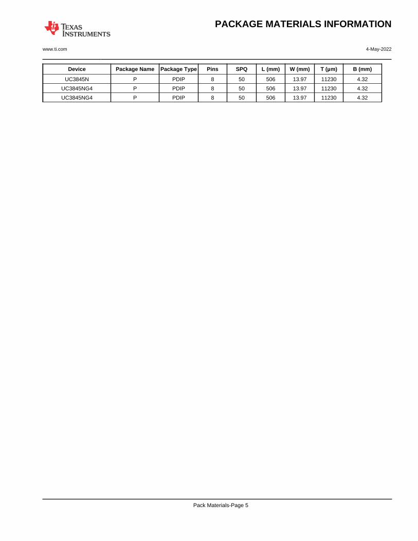
PACKAGE MATERIALS INFORMATION
www.ti.com 4-May-2022
Device Package Name Package Type Pins SPQ L (mm) W (mm) T (µm) B (mm)
UC3845N P PDIP 8 50 506 13.97 11230 4.32
UC3845NG4 P PDIP 8 50 506 13.97 11230 4.32
UC3845NG4 P PDIP 8 50 506 13.97 11230 4.32
Pack Materials-Page 5


www.ti.com
PACKAGE OUTLINE
C
.228-.244 TYP[5.80-6.19]
.069 MAX[1.75]
6X .050[1.27]
8X .012-.020 [0.31-0.51]
2X.150[3.81]
.005-.010 TYP[0.13-0.25]
0 - 8 .004-.010[0.11-0.25]
.010[0.25]
.016-.050[0.41-1.27]
4X (0 -15 )
A
.189-.197[4.81-5.00]
NOTE 3
B .150-.157[3.81-3.98]
NOTE 4
4X (0 -15 )
(.041)[1.04]
SOIC - 1.75 mm max heightD0008ASMALL OUTLINE INTEGRATED CIRCUIT
4214825/C 02/2019
NOTES: 1. Linear dimensions are in inches [millimeters]. Dimensions in parenthesis are for reference only. Controlling dimensions are in inches. Dimensioning and tolerancing per ASME Y14.5M. 2. This drawing is subject to change without notice. 3. This dimension does not include mold flash, protrusions, or gate burrs. Mold flash, protrusions, or gate burrs shall not exceed .006 [0.15] per side. 4. This dimension does not include interlead flash.5. Reference JEDEC registration MS-012, variation AA.
18
.010 [0.25] C A B
54
PIN 1 ID AREA
SEATING PLANE
.004 [0.1] C
SEE DETAIL A
DETAIL ATYPICAL
SCALE 2.800

www.ti.com
EXAMPLE BOARD LAYOUT
.0028 MAX[0.07]ALL AROUND
.0028 MIN[0.07]ALL AROUND
(.213)[5.4]
6X (.050 )[1.27]
8X (.061 )[1.55]
8X (.024)[0.6]
(R.002 ) TYP[0.05]
SOIC - 1.75 mm max heightD0008ASMALL OUTLINE INTEGRATED CIRCUIT
4214825/C 02/2019
NOTES: (continued) 6. Publication IPC-7351 may have alternate designs. 7. Solder mask tolerances between and around signal pads can vary based on board fabrication site.
METALSOLDER MASKOPENING
NON SOLDER MASKDEFINED
SOLDER MASK DETAILS
EXPOSEDMETAL
OPENINGSOLDER MASK METAL UNDER
SOLDER MASK
SOLDER MASKDEFINED
EXPOSEDMETAL
LAND PATTERN EXAMPLEEXPOSED METAL SHOWN
SCALE:8X
SYMM
1
45
8
SEEDETAILS
SYMM

www.ti.com
EXAMPLE STENCIL DESIGN
8X (.061 )[1.55]
8X (.024)[0.6]
6X (.050 )[1.27]
(.213)[5.4]
(R.002 ) TYP[0.05]
SOIC - 1.75 mm max heightD0008ASMALL OUTLINE INTEGRATED CIRCUIT
4214825/C 02/2019
NOTES: (continued) 8. Laser cutting apertures with trapezoidal walls and rounded corners may offer better paste release. IPC-7525 may have alternate design recommendations. 9. Board assembly site may have different recommendations for stencil design.
SOLDER PASTE EXAMPLEBASED ON .005 INCH [0.125 MM] THICK STENCIL
SCALE:8X
SYMM
SYMM
1
45
8

MECHANICAL DATA
MCER001A – JANUARY 1995 – REVISED JANUARY 1997
POST OFFICE BOX 655303 • DALLAS, TEXAS 75265
JG (R-GDIP-T8) CERAMIC DUAL-IN-LINE
0.310 (7,87)0.290 (7,37)
0.014 (0,36)0.008 (0,20)
Seating Plane
4040107/C 08/96
5
40.065 (1,65)0.045 (1,14)
8
1
0.020 (0,51) MIN
0.400 (10,16)0.355 (9,00)
0.015 (0,38)0.023 (0,58)
0.063 (1,60)0.015 (0,38)
0.200 (5,08) MAX
0.130 (3,30) MIN
0.245 (6,22)0.280 (7,11)
0.100 (2,54)
0°–15°
NOTES: A. All linear dimensions are in inches (millimeters).B. This drawing is subject to change without notice.C. This package can be hermetically sealed with a ceramic lid using glass frit.D. Index point is provided on cap for terminal identification.E. Falls within MIL STD 1835 GDIP1-T8


IMPORTANT NOTICE AND DISCLAIMERTI PROVIDES TECHNICAL AND RELIABILITY DATA (INCLUDING DATA SHEETS), DESIGN RESOURCES (INCLUDING REFERENCE DESIGNS), APPLICATION OR OTHER DESIGN ADVICE, WEB TOOLS, SAFETY INFORMATION, AND OTHER RESOURCES “AS IS” AND WITH ALL FAULTS, AND DISCLAIMS ALL WARRANTIES, EXPRESS AND IMPLIED, INCLUDING WITHOUT LIMITATION ANY IMPLIED WARRANTIES OF MERCHANTABILITY, FITNESS FOR A PARTICULAR PURPOSE OR NON-INFRINGEMENT OF THIRD PARTY INTELLECTUAL PROPERTY RIGHTS.These resources are intended for skilled developers designing with TI products. You are solely responsible for (1) selecting the appropriate TI products for your application, (2) designing, validating and testing your application, and (3) ensuring your application meets applicable standards, and any other safety, security, regulatory or other requirements.These resources are subject to change without notice. TI grants you permission to use these resources only for development of an application that uses the TI products described in the resource. Other reproduction and display of these resources is prohibited. No license is granted to any other TI intellectual property right or to any third party intellectual property right. TI disclaims responsibility for, and you will fully indemnify TI and its representatives against, any claims, damages, costs, losses, and liabilities arising out of your use of these resources.TI’s products are provided subject to TI’s Terms of Sale or other applicable terms available either on ti.com or provided in conjunction with such TI products. TI’s provision of these resources does not expand or otherwise alter TI’s applicable warranties or warranty disclaimers for TI products.TI objects to and rejects any additional or different terms you may have proposed. IMPORTANT NOTICE
Mailing Address: Texas Instruments, Post Office Box 655303, Dallas, Texas 75265Copyright © 2022, Texas Instruments Incorporated
Related Documents