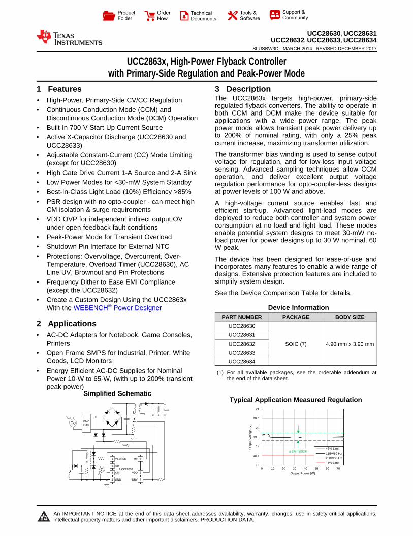
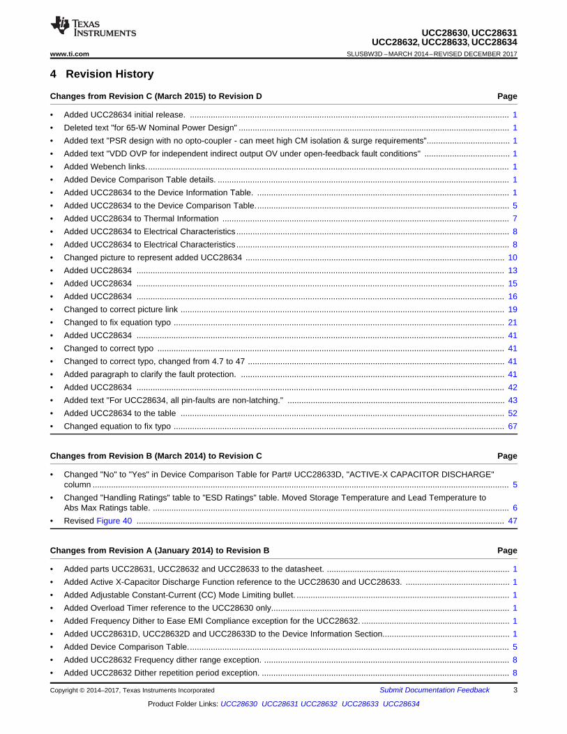
SD GND VSENSE CS HV VDD DRV UCC28630 1 2 3 4 8 6 5 EMC Filter t o VAC VOUT 18 18.5 19 19.5 20 20.5 21 0 10 20 30 40 50 60 70 Output Voltage (V) Output Power (W) +5% Limit 115V/60 Hz 230V/50 Hz –5% Limit C001 1% Typical Product Folder Order Now Technical Documents Tools & Software Support & Community An IMPORTANT NOTICE at the end of this data sheet addresses availability, warranty, changes, use in safety-critical applications, intellectual property matters and other important disclaimers. PRODUCTION DATA. UCC28630, UCC28631 UCC28632, UCC28633, UCC28634 SLUSBW3D – MARCH 2014 – REVISED DECEMBER 2017 UCC2863x, High-Power Flyback Controller with Primary-Side Regulation and Peak-Power Mode 1 1 Features 1• High-Power, Primary-Side CV/CC Regulation • Continuous Conduction Mode (CCM) and Discontinuous Conduction Mode (DCM) Operation • Built-In 700-V Start-Up Current Source • Active X-Capacitor Discharge (UCC28630 and UCC28633) • Adjustable Constant-Current (CC) Mode Limiting (except for UCC28630) • High Gate Drive Current 1-A Source and 2-A Sink • Low Power Modes for <30-mW System Standby • Best-In-Class Light Load (10%) Efficiency >85% • PSR design with no opto-coupler - can meet high CM isolation & surge requirements • VDD OVP for independent indirect output OV under open-feedback fault conditions • Peak-Power Mode for Transient Overload • Shutdown Pin Interface for External NTC • Protections: Overvoltage, Overcurrent, Over- Temperature, Overload Timer (UCC28630), AC Line UV, Brownout and Pin Protections • Frequency Dither to Ease EMI Compliance (except the UCC28632) • Create a Custom Design Using the UCC2863x With the WEBENCH ® Power Designer 2 Applications • AC-DC Adapters for Notebook, Game Consoles, Printers • Open Frame SMPS for Industrial, Printer, White Goods, LCD Monitors • Energy Efficient AC-DC Supplies for Nominal Power 10-W to 65-W, (with up to 200% transient peak power) 3 Description The UCC2863x targets high-power, primary-side regulated flyback converters. The ability to operate in both CCM and DCM make the device suitable for applications with a wide power range. The peak power mode allows transient peak power delivery up to 200% of nominal rating, with only a 25% peak current increase, maximizing transformer utilization. The transformer bias winding is used to sense output voltage for regulation, and for low-loss input voltage sensing. Advanced sampling techniques allow CCM operation, and deliver excellent output voltage regulation performance for opto-coupler-less designs at power levels of 100 W and above. A high-voltage current source enables fast and efficient start-up. Advanced light-load modes are deployed to reduce both controller and system power consumption at no load and light load. These modes enable potential system designs to meet 30-mW no- load power for power designs up to 30 W nominal, 60 W peak. The device has been designed for ease-of-use and incorporates many features to enable a wide range of designs. Extensive protection features are included to simplify system design. See the Device Comparison Table for details. Device Information PART NUMBER PACKAGE BODY SIZE UCC28630 SOIC (7) 4.90 mm x 3.90 mm UCC28631 UCC28632 UCC28633 UCC28634 (1) For all available packages, see the orderable addendum at the end of the data sheet. Simplified Schematic Typical Application Measured Regulation

Welcome message from author
This document is posted to help you gain knowledge. Please leave a comment to let me know what you think about it! Share it to your friends and learn new things together.
Transcript
SD
GND
VSENSE
CS
HV
VDD
DRV
UCC28630
1
2
3
4
8
6
5
EMCFilter
to
VAC
VOUT
18
18.5
19
19.5
20
20.5
21
0 10 20 30 40 50 60 70
Out
put
Vol
tage
(V
)
Output Power (W)
+5% Limit
115V/60 Hz
230V/50 Hz
±5% Limit
C001
1% Typical
Product
Folder
Order
Now
Technical
Documents
Tools &
Software
Support &Community
An IMPORTANT NOTICE at the end of this data sheet addresses availability, warranty, changes, use in safety-critical applications,intellectual property matters and other important disclaimers. PRODUCTION DATA.
UCC28630, UCC28631UCC28632, UCC28633, UCC28634
SLUSBW3D –MARCH 2014–REVISED DECEMBER 2017
UCC2863x, High-Power Flyback Controllerwith Primary-Side Regulation and Peak-Power Mode
1
1 Features1• High-Power, Primary-Side CV/CC Regulation• Continuous Conduction Mode (CCM) and
Discontinuous Conduction Mode (DCM) Operation• Built-In 700-V Start-Up Current Source• Active X-Capacitor Discharge (UCC28630 and
UCC28633)• Adjustable Constant-Current (CC) Mode Limiting
(except for UCC28630)• High Gate Drive Current 1-A Source and 2-A Sink• Low Power Modes for <30-mW System Standby• Best-In-Class Light Load (10%) Efficiency >85%• PSR design with no opto-coupler - can meet high
CM isolation & surge requirements• VDD OVP for independent indirect output OV
under open-feedback fault conditions• Peak-Power Mode for Transient Overload• Shutdown Pin Interface for External NTC• Protections: Overvoltage, Overcurrent, Over-
Temperature, Overload Timer (UCC28630), ACLine UV, Brownout and Pin Protections
• Frequency Dither to Ease EMI Compliance(except the UCC28632)
• Create a Custom Design Using the UCC2863xWith the WEBENCH® Power Designer
2 Applications• AC-DC Adapters for Notebook, Game Consoles,
Printers• Open Frame SMPS for Industrial, Printer, White
Goods, LCD Monitors• Energy Efficient AC-DC Supplies for Nominal
Power 10-W to 65-W, (with up to 200% transientpeak power)
3 DescriptionThe UCC2863x targets high-power, primary-sideregulated flyback converters. The ability to operate inboth CCM and DCM make the device suitable forapplications with a wide power range. The peakpower mode allows transient peak power delivery upto 200% of nominal rating, with only a 25% peakcurrent increase, maximizing transformer utilization.
The transformer bias winding is used to sense outputvoltage for regulation, and for low-loss input voltagesensing. Advanced sampling techniques allow CCMoperation, and deliver excellent output voltageregulation performance for opto-coupler-less designsat power levels of 100 W and above.
A high-voltage current source enables fast andefficient start-up. Advanced light-load modes aredeployed to reduce both controller and system powerconsumption at no load and light load. These modesenable potential system designs to meet 30-mW no-load power for power designs up to 30 W nominal, 60W peak.
The device has been designed for ease-of-use andincorporates many features to enable a wide range ofdesigns. Extensive protection features are included tosimplify system design.
See the Device Comparison Table for details.
Device InformationPART NUMBER PACKAGE BODY SIZE
UCC28630
SOIC (7) 4.90 mm x 3.90 mmUCC28631UCC28632UCC28633UCC28634
(1) For all available packages, see the orderable addendum atthe end of the data sheet.
Simplified SchematicTypical Application Measured Regulation
2
UCC28630, UCC28631UCC28632, UCC28633, UCC28634SLUSBW3D –MARCH 2014–REVISED DECEMBER 2017 www.ti.com
Product Folder Links: UCC28630 UCC28631 UCC28632 UCC28633 UCC28634
Submit Documentation Feedback Copyright © 2014–2017, Texas Instruments Incorporated
Table of Contents1 Features .................................................................. 12 Applications ........................................................... 13 Description ............................................................. 14 Revision History..................................................... 35 Device Comparison Table ..................................... 56 Pin Configuration and Functions ......................... 57 Specifications......................................................... 6
7.1 Absolute Maximum Ratings ...................................... 67.2 ESD Ratings.............................................................. 67.3 Recommended Operating Conditions....................... 67.4 Thermal Information (UCC28630, UCC28631)......... 77.5 Thermal Information (UCC28632, UCC28633,
(UCC28630, UCC28634) ........................................... 77.6 Electrical Characteristics........................................... 87.7 Typical Characteristics ............................................ 10
8 Detailed Description ............................................ 138.1 Overview ................................................................. 138.2 Functional Block Diagram ....................................... 148.3 Feature Description................................................. 15
8.4 Device Functional Modes........................................ 529 Applications and Implementation ...................... 53
9.1 Application Information............................................ 539.2 Typical Application ................................................. 539.3 Dos and Don'ts........................................................ 73
10 Power Supply Recommendations ..................... 7311 Layout................................................................... 74
11.1 Layout Guidelines ................................................. 7411.2 Layout Example .................................................... 75
12 Device and Documentation Support ................. 7612.1 Device Support...................................................... 7612.2 Documentation Support ........................................ 7612.3 Receiving Notification of Documentation Updates 7612.4 Community Resources.......................................... 7612.5 Trademarks ........................................................... 7712.6 Electrostatic Discharge Caution............................ 7712.7 Glossary ................................................................ 77
13 Mechanical, Packaging, and OrderableInformation ........................................................... 77
3
UCC28630, UCC28631UCC28632, UCC28633, UCC28634
www.ti.com SLUSBW3D –MARCH 2014–REVISED DECEMBER 2017
Product Folder Links: UCC28630 UCC28631 UCC28632 UCC28633 UCC28634
Submit Documentation FeedbackCopyright © 2014–2017, Texas Instruments Incorporated
4 Revision History
Changes from Revision C (March 2015) to Revision D Page
• Added UCC28634 initial release. .......................................................................................................................................... 1• Deleted text "for 65-W Nominal Power Design" ..................................................................................................................... 1• Added text "PSR design with no opto-coupler - can meet high CM isolation & surge requirements".................................... 1• Added text "VDD OVP for independent indirect output OV under open-feedback fault conditions" ..................................... 1• Added Webench links. ............................................................................................................................................................ 1• Added Device Comparison Table details. .............................................................................................................................. 1• Added UCC28634 to the Device Information Table. ............................................................................................................. 1• Added UCC28634 to the Device Comparison Table.............................................................................................................. 5• Added UCC28634 to Thermal Information ............................................................................................................................ 7• Added UCC28634 to Electrical Characteristics ...................................................................................................................... 8• Added UCC28634 to Electrical Characteristics ...................................................................................................................... 8• Changed picture to represent added UCC28634 ................................................................................................................ 10• Added UCC28634 ............................................................................................................................................................... 13• Added UCC28634 ............................................................................................................................................................... 15• Added UCC28634 ............................................................................................................................................................... 16• Changed to correct picture link ............................................................................................................................................ 19• Changed to fix equation typo ............................................................................................................................................... 21• Added UCC28634 ............................................................................................................................................................... 41• Changed to correct typo ...................................................................................................................................................... 41• Changed to correct typo, changed from 4.7 to 47 ............................................................................................................... 41• Added paragraph to clarify the fault protection. .................................................................................................................. 41• Added UCC28634 ............................................................................................................................................................... 42• Added text "For UCC28634, all pin-faults are non-latching." .............................................................................................. 43• Added UCC28634 to the table ............................................................................................................................................ 52• Changed equation to fix typo ............................................................................................................................................... 67
Changes from Revision B (March 2014) to Revision C Page
• Changed "No" to "Yes" in Device Comparison Table for Part# UCC28633D, "ACTIVE-X CAPACITOR DISCHARGE"column .................................................................................................................................................................................... 5
• Changed "Handling Ratings" table to "ESD Ratings" table. Moved Storage Temperature and Lead Temperature toAbs Max Ratings table. .......................................................................................................................................................... 6
• Revised Figure 40 ............................................................................................................................................................... 47
Changes from Revision A (January 2014) to Revision B Page
• Added parts UCC28631, UCC28632 and UCC28633 to the datasheet. ............................................................................... 1• Added Active X-Capacitor Discharge Function reference to the UCC28630 and UCC28633. ............................................. 1• Added Adjustable Constant-Current (CC) Mode Limiting bullet. ............................................................................................ 1• Added Overload Timer reference to the UCC28630 only....................................................................................................... 1• Added Frequency Dither to Ease EMI Compliance exception for the UCC28632. ................................................................ 1• Added UCC28631D, UCC28632D and UCC28633D to the Device Information Section....................................................... 1• Added Device Comparison Table........................................................................................................................................... 5• Added UCC28632 Frequency dither range exception. .......................................................................................................... 8• Added UCC28632 Dither repetition period exception. ........................................................................................................... 8
4
UCC28630, UCC28631UCC28632, UCC28633, UCC28634SLUSBW3D –MARCH 2014–REVISED DECEMBER 2017 www.ti.com
Product Folder Links: UCC28630 UCC28631 UCC28632 UCC28633 UCC28634
Submit Documentation Feedback Copyright © 2014–2017, Texas Instruments Incorporated
• Added UCC28633 Wake-up level (rising) exception. ............................................................................................................. 8• Added UCC28633 SD VWAKE(rise) vs. Temperature exception............................................................................................... 12• Added text to the, "The controller operates in either DCM and CCM..." paragraph. .......................................................... 13• Changed the "Supply the device bias power during latched fault mode" bullet. .................................................................. 15• Added UCC28630 and UCC28633 only exception to the "AC sense input for X-capacitor discharge detect" bullet. ......... 15• Changed HV Pin Connection diagram. ............................................................................................................................... 15• Added sentence, "In the UCC28631 and the UCC28632, the HV pin can connect to either the AC or DC side of the
bridge.".................................................................................................................................................................................. 16• Added VIN(avg) definition. ................................................................................................................................................... 16• Added (UCC28630 and UCC28633 only) to the Active X-Capacitor Discharge section...................................................... 19• Added UCC28633 to the Improved Performance with UCC28630 section.......................................................................... 20• Added UCC28631, UCC28632 and the UCC28633 IOUT(lim) adjustment note. .................................................................... 37• Added UCC28630 only note to the Primary-Side Overload Timer section. ......................................................................... 38• Added UCC28630 only note added to the Overload Timer Adjustment section. ................................................................ 40• Added CC-Mode IOUT(lim) Adjustment section. ...................................................................................................................... 41• Added UCC28631, UCC28632 and the UCC28633 to the Fault Sources and Associated Responses table. .................... 42• Added The fault response (latching or auto recovery) depends on the device variant, per Table 3. ................................. 44• Added The fault response (latching or recovery) depends on the device variant, per Table 3. ......................................... 44• Added UCC28633 exception to the External SD Pin Wake Input section. .......................................................................... 45• Added External Wake Input at VSENSE Pin (UCC28633 Only) section.............................................................................. 46• Added UCC28632 exception to the Frequency Dither For EMI section............................................................................... 51• Added External Wake Pulse Calculation at VSENSE Pin (UCC28633 Only) section.......................................................... 66
Changes from Original (January 2014) to Revision A Page
• Changed marketing status from Product Preview to Production Data. .................................................................................. 1
HV
VDD
DRV
1
2
3
4
8
6
5
VSENSE
SD
CS
GND
5
UCC28630, UCC28631UCC28632, UCC28633, UCC28634
www.ti.com SLUSBW3D –MARCH 2014–REVISED DECEMBER 2017
Product Folder Links: UCC28630 UCC28631 UCC28632 UCC28633 UCC28634
Submit Documentation FeedbackCopyright © 2014–2017, Texas Instruments Incorporated
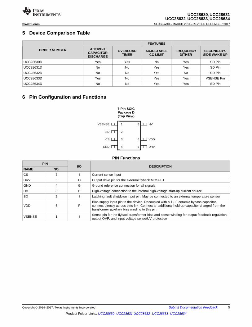
5 Device Comparison Table
ORDER NUMBER
FEATURESACTIVE-X
CAPACITORDISCHARGE
OVERLOADTIMER
ADJUSTABLECC LIMIT
FREQUENCYDITHER
SECONDARY-SIDE WAKE UP
UCC28630D Yes Yes No Yes SD PinUCC28631D No No Yes Yes SD PinUCC28632D No No Yes No SD PinUCC28633D Yes No Yes Yes VSENSE PinUCC28634D No No Yes Yes SD Pin
6 Pin Configuration and Functions
7-Pin SOICPackage D(Top View)
PIN FunctionsPIN
I/O DESCRIPTIONNAME NO.CS 3 I Current sense inputDRV 5 O Output drive pin for the external flyback MOSFETGND 4 G Ground reference connection for all signalsHV 8 P High-voltage connection to the internal high-voltage start-up current sourceSD 2 I Latching fault shutdown input pin. May be connected to an external temperature sensor
VDD 6 PBias supply input pin to the device. Decoupled with a 1-µF ceramic bypass capacitor,connect directly across pins 6-4. Connect an additional hold-up capacitor charged from thetransformer auxiliary bias winding to this pin.
VSENSE 1 I Sense pin for the flyback transformer bias and sense winding for output feedback regulation,output OVP, and input voltage sense/UV protection
6
UCC28630, UCC28631UCC28632, UCC28633, UCC28634SLUSBW3D –MARCH 2014–REVISED DECEMBER 2017 www.ti.com
Product Folder Links: UCC28630 UCC28631 UCC28632 UCC28633 UCC28634
Submit Documentation Feedback Copyright © 2014–2017, Texas Instruments Incorporated
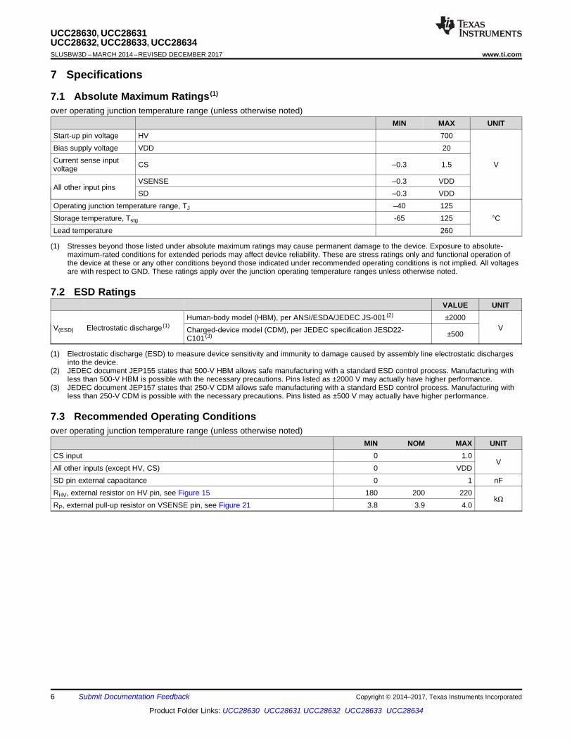
(1) Stresses beyond those listed under absolute maximum ratings may cause permanent damage to the device. Exposure to absolute-maximum-rated conditions for extended periods may affect device reliability. These are stress ratings only and functional operation ofthe device at these or any other conditions beyond those indicated under recommended operating conditions is not implied. All voltagesare with respect to GND. These ratings apply over the junction operating temperature ranges unless otherwise noted.
7 Specifications
7.1 Absolute Maximum Ratings (1)
over operating junction temperature range (unless otherwise noted)MIN MAX UNIT
Start-up pin voltage HV 700
V
Bias supply voltage VDD 20Current sense inputvoltage CS –0.3 1.5
All other input pinsVSENSE –0.3 VDDSD –0.3 VDD
Operating junction temperature range, TJ –40 125°CStorage temperature, Tstg -65 125
Lead temperature 260
(1) Electrostatic discharge (ESD) to measure device sensitivity and immunity to damage caused by assembly line electrostatic dischargesinto the device.
(2) JEDEC document JEP155 states that 500-V HBM allows safe manufacturing with a standard ESD control process. Manufacturing withless than 500-V HBM is possible with the necessary precautions. Pins listed as ±2000 V may actually have higher performance.
(3) JEDEC document JEP157 states that 250-V CDM allows safe manufacturing with a standard ESD control process. Manufacturing withless than 250-V CDM is possible with the necessary precautions. Pins listed as ±500 V may actually have higher performance.
7.2 ESD RatingsVALUE UNIT
V(ESD) Electrostatic discharge (1)Human-body model (HBM), per ANSI/ESDA/JEDEC JS-001 (2) ±2000
VCharged-device model (CDM), per JEDEC specification JESD22-C101 (3) ±500
7.3 Recommended Operating Conditionsover operating junction temperature range (unless otherwise noted)
MIN NOM MAX UNITCS input 0 1.0
VAll other inputs (except HV, CS) 0 VDDSD pin external capacitance 0 1 nFRHV, external resistor on HV pin, see Figure 15 180 200 220
kΩRP, external pull-up resistor on VSENSE pin, see Figure 21 3.8 3.9 4.0
7
UCC28630, UCC28631UCC28632, UCC28633, UCC28634
www.ti.com SLUSBW3D –MARCH 2014–REVISED DECEMBER 2017
Product Folder Links: UCC28630 UCC28631 UCC28632 UCC28633 UCC28634
Submit Documentation FeedbackCopyright © 2014–2017, Texas Instruments Incorporated
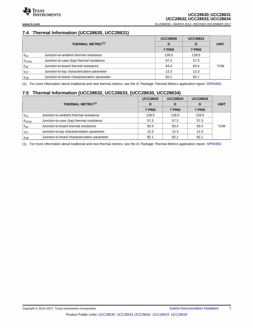
(1) For more information about traditional and new thermal metrics, see the IC Package Thermal Metrics application report, SPRA953.
7.4 Thermal Information (UCC28630, UCC28631)
THERMAL METRIC (1)UCC28630 UCC28631
UNITD D7 PINS 7 PINS
θJA Junction-to-ambient thermal resistance 128.5 128.5
°C/WθJCtop Junction-to-case (top) thermal resistance 57.3 57.3θJB Junction-to-board thermal resistance 83.4 83.4ψJT Junction-to-top characterization parameter 12.3 12.3ψJB Junction-to-board characterization parameter 82.1 82.1
(1) For more information about traditional and new thermal metrics, see the IC Package Thermal Metrics application report, SPRA953.
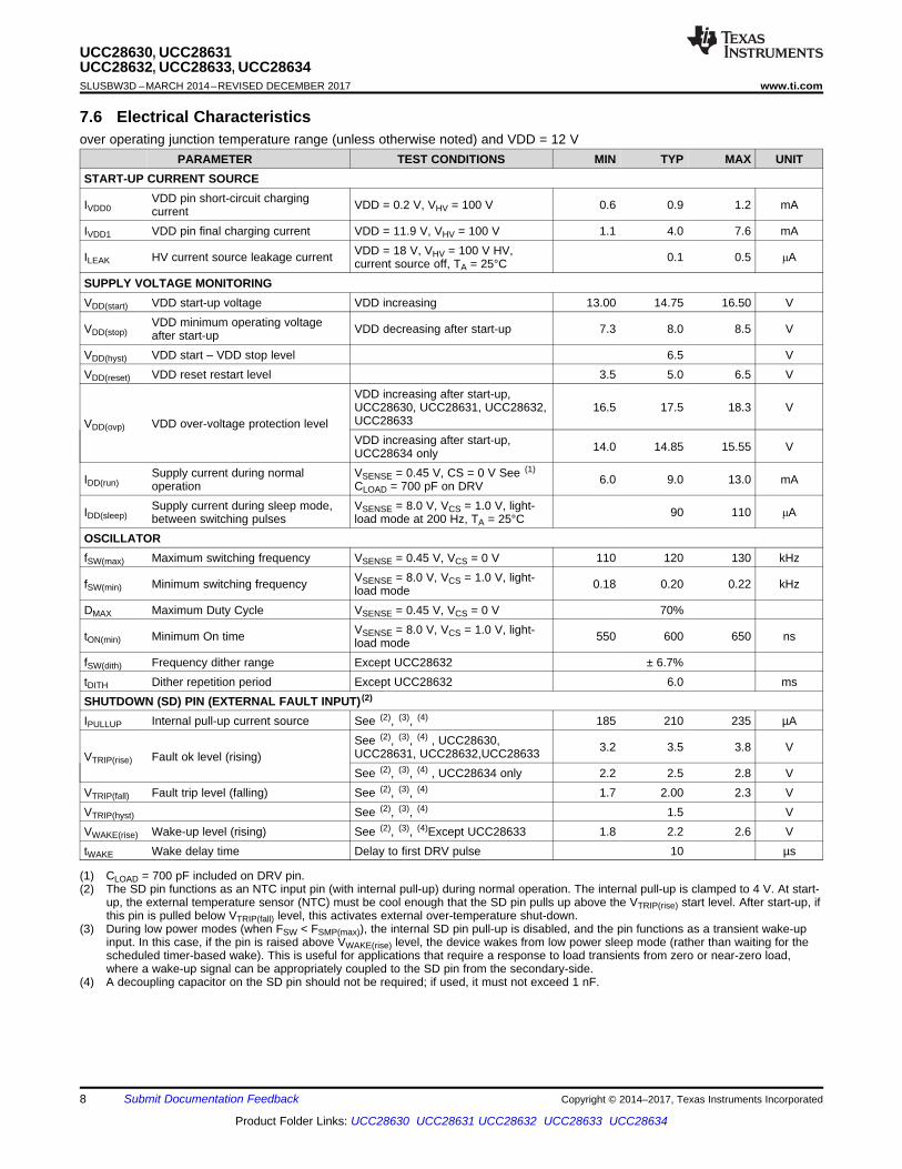
7.5 Thermal Information (UCC28632, UCC28633, (UCC28630, UCC28634)
THERMAL METRIC (1)UCC28632 UCC28633 UCC28634
UNITD D D7 PINS 7 PINS 7 PINS
θJA Junction-to-ambient thermal resistance 128.5 128.5 128.5
°C/WθJCtop Junction-to-case (top) thermal resistance 57.3 57.3 57.3θJB Junction-to-board thermal resistance 83.4 83.4 83.4ψJT Junction-to-top characterization parameter 12.3 12.3 12.3ψJB Junction-to-board characterization parameter 82.1 82.1 82.1
8
UCC28630, UCC28631UCC28632, UCC28633, UCC28634SLUSBW3D –MARCH 2014–REVISED DECEMBER 2017 www.ti.com
Product Folder Links: UCC28630 UCC28631 UCC28632 UCC28633 UCC28634
Submit Documentation Feedback Copyright © 2014–2017, Texas Instruments Incorporated
(1) CLOAD = 700 pF included on DRV pin.(2) The SD pin functions as an NTC input pin (with internal pull-up) during normal operation. The internal pull-up is clamped to 4 V. At start-
up, the external temperature sensor (NTC) must be cool enough that the SD pin pulls up above the VTRIP(rise) start level. After start-up, ifthis pin is pulled below VTRIP(fall) level, this activates external over-temperature shut-down.
(3) During low power modes (when FSW < FSMP(max)), the internal SD pin pull-up is disabled, and the pin functions as a transient wake-upinput. In this case, if the pin is raised above VWAKE(rise) level, the device wakes from low power sleep mode (rather than waiting for thescheduled timer-based wake). This is useful for applications that require a response to load transients from zero or near-zero load,where a wake-up signal can be appropriately coupled to the SD pin from the secondary-side.
(4) A decoupling capacitor on the SD pin should not be required; if used, it must not exceed 1 nF.
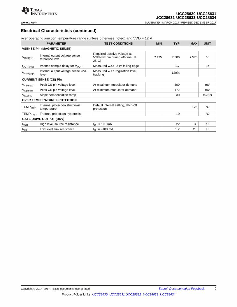
7.6 Electrical Characteristicsover operating junction temperature range (unless otherwise noted) and VDD = 12 V
PARAMETER TEST CONDITIONS MIN TYP MAX UNITSTART-UP CURRENT SOURCE
IVDD0VDD pin short-circuit chargingcurrent VDD = 0.2 V, VHV = 100 V 0.6 0.9 1.2 mA
IVDD1 VDD pin final charging current VDD = 11.9 V, VHV = 100 V 1.1 4.0 7.6 mA
ILEAK HV current source leakage current VDD = 18 V, VHV = 100 V HV,current source off, TA = 25°C 0.1 0.5 μA
SUPPLY VOLTAGE MONITORINGVDD(start) VDD start-up voltage VDD increasing 13.00 14.75 16.50 V
VDD(stop)VDD minimum operating voltageafter start-up VDD decreasing after start-up 7.3 8.0 8.5 V
VDD(hyst) VDD start – VDD stop level 6.5 VVDD(reset) VDD reset restart level 3.5 5.0 6.5 V
VDD(ovp) VDD over-voltage protection level
VDD increasing after start-up,UCC28630, UCC28631, UCC28632,UCC28633
16.5 17.5 18.3 V
VDD increasing after start-up,UCC28634 only 14.0 14.85 15.55 V
IDD(run)Supply current during normaloperation
VSENSE = 0.45 V, CS = 0 V See (1)
CLOAD = 700 pF on DRV 6.0 9.0 13.0 mA
IDD(sleep)Supply current during sleep mode,between switching pulses
VSENSE = 8.0 V, VCS = 1.0 V, light-load mode at 200 Hz, TA = 25°C 90 110 μA
OSCILLATORfSW(max) Maximum switching frequency VSENSE = 0.45 V, VCS = 0 V 110 120 130 kHz
fSW(min) Minimum switching frequency VSENSE = 8.0 V, VCS = 1.0 V, light-load mode 0.18 0.20 0.22 kHz
DMAX Maximum Duty Cycle VSENSE = 0.45 V, VCS = 0 V 70%
tON(min) Minimum On time VSENSE = 8.0 V, VCS = 1.0 V, light-load mode 550 600 650 ns
fSW(dith) Frequency dither range Except UCC28632 ± 6.7%tDITH Dither repetition period Except UCC28632 6.0 msSHUTDOWN (SD) PIN (EXTERNAL FAULT INPUT) (2)
IPULLUP Internal pull-up current source See (2), (3), (4) 185 210 235 µA
VTRIP(rise) Fault ok level (rising)See (2), (3), (4) , UCC28630,UCC28631, UCC28632,UCC28633 3.2 3.5 3.8 V
See (2), (3), (4) , UCC28634 only 2.2 2.5 2.8 VVTRIP(fall) Fault trip level (falling) See (2), (3), (4) 1.7 2.00 2.3 VVTRIP(hyst) See (2), (3), (4) 1.5 VVWAKE(rise) Wake-up level (rising) See (2), (3), (4)Except UCC28633 1.8 2.2 2.6 VtWAKE Wake delay time Delay to first DRV pulse 10 µs
9
UCC28630, UCC28631UCC28632, UCC28633, UCC28634
www.ti.com SLUSBW3D –MARCH 2014–REVISED DECEMBER 2017
Product Folder Links: UCC28630 UCC28631 UCC28632 UCC28633 UCC28634
Submit Documentation FeedbackCopyright © 2014–2017, Texas Instruments Incorporated
Electrical Characteristics (continued)over operating junction temperature range (unless otherwise noted) and VDD = 12 V
PARAMETER TEST CONDITIONS MIN TYP MAX UNITVSENSE Pin (MAGNETIC SENSE)
VOUT(ref)Internal output voltage sensereference level
Required positive voltage atVSENSE pin during off-time (at25°C)
7.425 7.500 7.575 V
tOUT(smp) Vsense sample delay for VOUT Measured w.r.t. DRV falling edge 1.7 µs
VOUT(ovp)Internal output voltage sense OVPlevel
Measured w.r.t. regulation level,tracking 120%
CURRENT SENSE (CS) PinVCS(max) Peak CS pin voltage level At maximum modulator demand 800 mVVCS(min) Peak CS pin voltage level At minimum modulator demand 172 mVVSLOPE Slope compensation ramp 30 mV/µsOVER TEMPERATURE PROTECTION
TEMPTRIPThermal protection shutdowntemperature
Default internal setting, latch-offprotection 125 °C
TEMPHYST Thermal protection hysteresis 10 °CGATE DRIVE OUTPUT (DRV)ROH High level source resistance IOH = 100 mA 22 35 Ω
ROL Low level sink resistance IOL = –100 mA 1.2 2.5 Ω
Temperature (oC)
Nor
mal
ized
VD
D(o
vp) T
hres
hold
s
-50 0 50 100 1500.97
0.976
0.982
0.988
0.994
1
1.006
1.012
1.018
1.024
1.03
1.036
D001
7.7
7.75
7.8
7.85
7.9
7.95
8
8.05
8.1
8.15
8.2
±50 0 50 100 150
Vol
tage
(V
)
Temperature (C) C006
7
7.5
8
8.5
9
9.5
10
10.5
11
11.5
12
±50 0 50 100 150
Cur
rent
(m
A)
Temperature (C) C004
14.6
14.65
14.7
14.75
14.8
14.85
14.9
±50 0 50 100 150
Vol
tage
(V
)
Temperature (C) C005
0.95
0.955
0.96
0.965
0.97
0.975
0.98
0.985
0.99
0.995
1
±50 0 50 100 150
Cur
rent
(m
A)
Temperature (C) C002
3
3.1
3.2
3.3
3.4
3.5
3.6
3.7
3.8
3.9
4
±50 0 50 100 150
Cur
rent
(m
A)
Temperature (C) C003
10
UCC28630, UCC28631UCC28632, UCC28633, UCC28634SLUSBW3D –MARCH 2014–REVISED DECEMBER 2017 www.ti.com
Product Folder Links: UCC28630 UCC28631 UCC28632 UCC28633 UCC28634
Submit Documentation Feedback Copyright © 2014–2017, Texas Instruments Incorporated
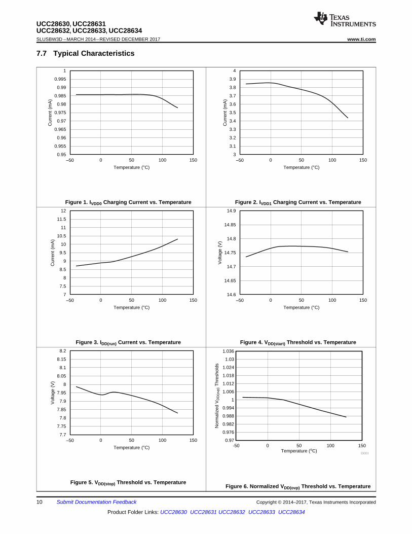
7.7 Typical Characteristics
Figure 1. IVDD0 Charging Current vs. Temperature Figure 2. IVDD1 Charging Current vs. Temperature
Figure 3. IDD(run) Current vs. Temperature Figure 4. VDD(start) Threshold vs. Temperature
Figure 5. VDD(stop) Threshold vs. TemperatureFigure 6. Normalized VDD(ovp) Threshold vs. Temperature
0.98
0.985
0.99
0.995
1
1.005
1.01
1.015
1.02
±50 0 50 100 150
DR
V M
easu
re G
ain
(Nor
mal
ized
) (d
B)
Temperature (C) C012
207
208
209
210
211
212
±50 0 50 100 150
Cur
rent
(
A)
Temperature (C) C013
115
116
117
118
119
120
121
122
±50 0 50 100 150
Fre
quen
cy (
kHz)
Temperature (C) C010
195
196
197
198
199
200
201
202
203
204
205
±50 0 50 100 150
Fre
quen
cy (
Hz)
Temperature (C) C011
4.5
4.55
4.6
4.65
4.7
4.75
4.8
4.85
4.9
4.95
5
±50 0 50 100 150
Vol
tage
(V
)
Temperature (C) C008
7.4
7.42
7.44
7.46
7.48
7.5
7.52
7.54
7.56
7.58
7.6
±50 0 50 100 150
Vol
tage
(V
)
Temperature (C) C009
11
UCC28630, UCC28631UCC28632, UCC28633, UCC28634
www.ti.com SLUSBW3D –MARCH 2014–REVISED DECEMBER 2017
Product Folder Links: UCC28630 UCC28631 UCC28632 UCC28633 UCC28634
Submit Documentation FeedbackCopyright © 2014–2017, Texas Instruments Incorporated
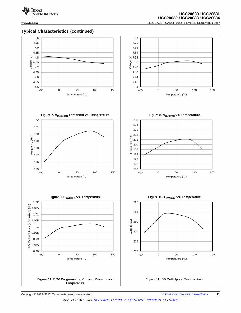
Typical Characteristics (continued)
Figure 7. VDD(reset) Threshold vs. Temperature Figure 8. VOUT(ref) vs. Temperature
Figure 9. FSW(max) vs. Temperature Figure 10. FSW(min) vs. Temperature
Figure 11. DRV Programming Current Measure vs.Temperature
Figure 12. SD Pull-Up vs. Temperature
1.9
1.92
1.94
1.96
1.98
2
2.02
2.04
±50 0 50 100 150
Vol
tage
(V
)
Temperature (C) C014
2.15
2.17
2.19
2.21
2.23
2.25
±50 0 50 100 150
Vol
tage
(V
)
Temperature (C) C015
12
UCC28630, UCC28631UCC28632, UCC28633, UCC28634SLUSBW3D –MARCH 2014–REVISED DECEMBER 2017 www.ti.com
Product Folder Links: UCC28630 UCC28631 UCC28632 UCC28633 UCC28634
Submit Documentation Feedback Copyright © 2014–2017, Texas Instruments Incorporated
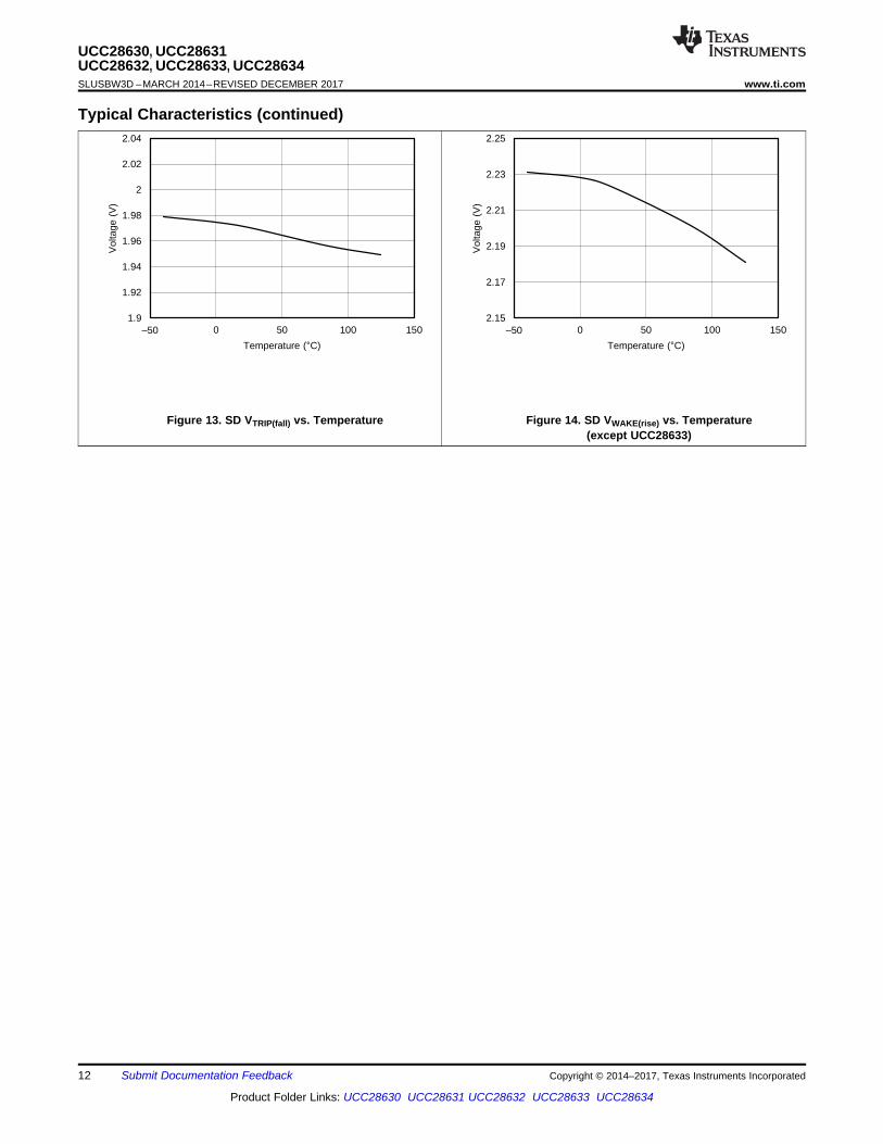
Typical Characteristics (continued)
Figure 13. SD VTRIP(fall) vs. Temperature Figure 14. SD VWAKE(rise) vs. Temperature(except UCC28633)
13
UCC28630, UCC28631UCC28632, UCC28633, UCC28634
www.ti.com SLUSBW3D –MARCH 2014–REVISED DECEMBER 2017
Product Folder Links: UCC28630 UCC28631 UCC28632 UCC28633 UCC28634
Submit Documentation FeedbackCopyright © 2014–2017, Texas Instruments Incorporated
8 Detailed Description
8.1 OverviewThe UCC28630, UCC28631, UCC28633, UCC28633 and UCC28634 family of devices are highly-integrated,primary-side-regulated (PSR) flyback controllers. The device supports magnetically-sensed output voltageregulation via the transformer bias winding. This feature eliminates the need for a secondary-side reference,error amplifier and opto-isolator. The device employs an advanced internal control algorithm that offers accuratestatic output voltage regulation against line and load. The fixed-point, magnetic-sampling scheme allowsoperation in both continuous conduction mode (CCM) and discontinuous conduction mode (DCM). Additionally,the device achieves accurate constant-current (CC) control of the output current limit using only primary-side,current sensing. Uniquely, this CC function operates seamlessly as the operating mode changes between DCMand CCM operation.
The controller includes an internal, high-voltage (HV) start-up current-source, and employs low-power sleepmodes and switching frequency reduction, to improve light-load efficiency and standby power. The devicetypically achieves standby power levels between 0.05% and 0.1% of peak output power.
The controller operates in either DCM and CCM, using a mix of peak current-mode PWM (AM) and switching-frequency modulation (FM) schemes. The control approach improves performance (efficiency, size and cost) andcan reduce transformer size and cost by allowing operation in CCM with FM during peak overload conditions.Extensive protection features are incorporated, including output overvoltage protection (OVP), bias railovervoltage and undervoltage (OV/UV), active X-capacitor discharge, line undervoltage and brownout protection,overcurrent overload timer, open- and short-circuit pin protections, peak current adjustment with line andfrequency dither for system EMI reduction. The various devices in the UCC2863x family offer a different mix offeatures to suit a wide range of applications and requirements.
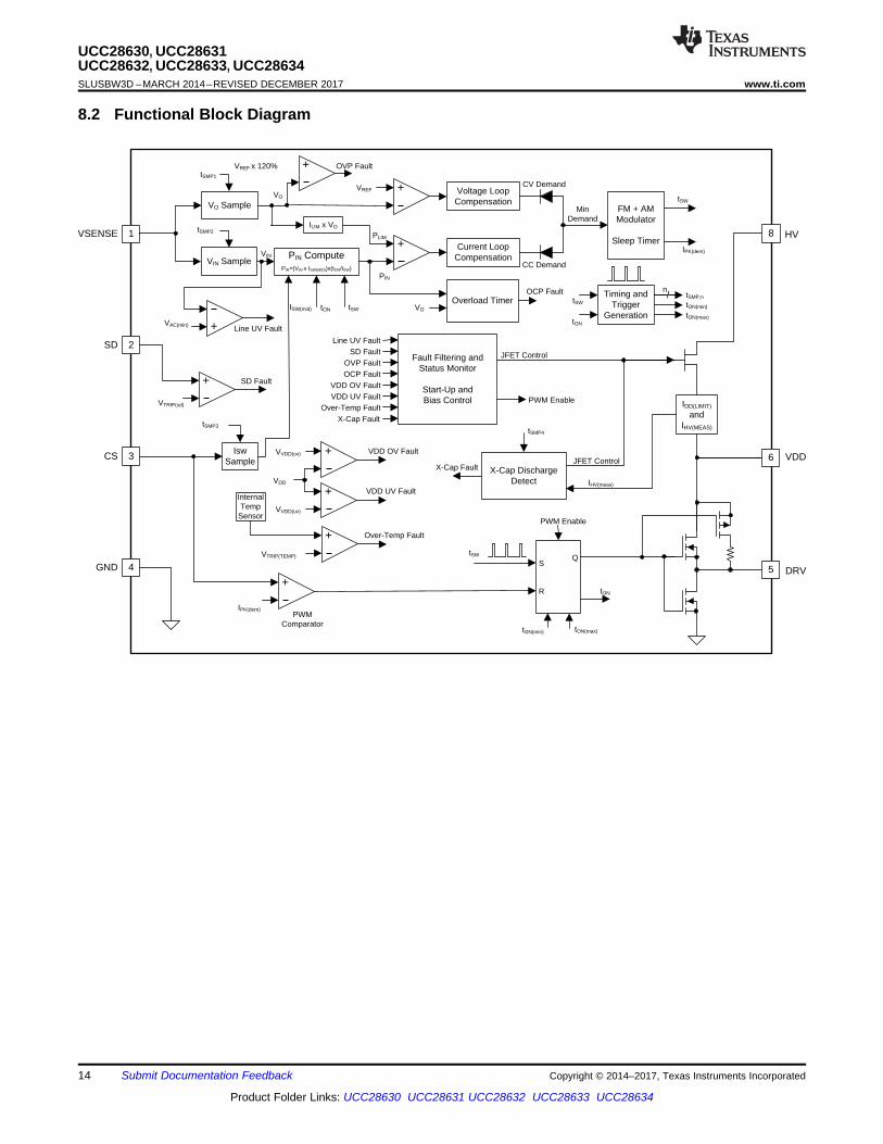
HV
VDD
DRV
VO Sample
VIN Sample
VREF Voltage Loop Compensation
CV Demand
Isw Sample
PIN ComputePIN=(VIN x ISW(MID))x(tON/tSW)
VIN
ISW(mid) tON tSW
VO
PIN
PLIM
+
ILIM x VO
Current Loop Compensation
CC Demand
+
+VREF x 120% OVP Fault
FM + AM Modulator
Sleep Timer
+
tSW
IPK(dem)
IDD(LIMIT) and
IHV(MEAS)
Fault Filtering and Status Monitor
Start-Up and Bias Control
PWM Comparator
+
VTRIP(sd)
SD Fault
QS
R
IPK(dem)
SD FaultOVP Fault
Overload TimerOCP Fault
OCP Fault
+
VTRIP(TEMP)
Internal Temp
Sensor
Over-Temp Fault
tON(max)tON(min)
tON
tSMP1
tSMP2
tSMP3
+
+VDD
VVDD(ov)
VVDD(uv)
VDD OV Fault
VDD UV Fault
VDD OV FaultVDD UV Fault
Over-Temp Fault
Timing and Trigger
Generation
/
tON(max)
tON(min)
tSMP,nn
X-Cap Fault
tSW
JFET Control
PWM Enable
PWM Enable
X-Cap Discharge Detect
JFET Control
IHV(meas)
tSMP4
X-Cap Fault
tSW
tON+VAC(min) Line UV Fault
Line UV Fault
Min Demand
VO
4GND
3CS
2SD
1VSENSE
5
6
8
14
UCC28630, UCC28631UCC28632, UCC28633, UCC28634SLUSBW3D –MARCH 2014–REVISED DECEMBER 2017 www.ti.com
Product Folder Links: UCC28630 UCC28631 UCC28632 UCC28633 UCC28634
Submit Documentation Feedback Copyright © 2014–2017, Texas Instruments Incorporated
8.2 Functional Block Diagram
(a) AC-side (b) DC-side
SD
GND
VSENSE
CS
HV
VDD
DRV
UCC2863X
1
2
3
4
8
6
5
EMCFilter
RHV
VAC
SD
GND
VSENSE
CS
HV
VDD
DRV
UCC2863X
1
2
3
4
8
6
5
EMCFilter
RHV
VAC
15
UCC28630, UCC28631UCC28632, UCC28633, UCC28634
www.ti.com SLUSBW3D –MARCH 2014–REVISED DECEMBER 2017
Product Folder Links: UCC28630 UCC28631 UCC28632 UCC28633 UCC28634
Submit Documentation FeedbackCopyright © 2014–2017, Texas Instruments Incorporated
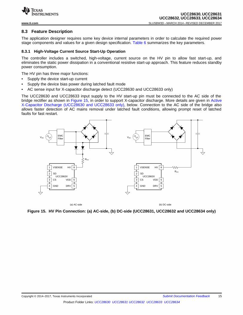
8.3 Feature DescriptionThe application designer requires some key device internal parameters in order to calculate the required powerstage components and values for a given design specification. Table 6 summarizes the key parameters.
8.3.1 High-Voltage Current Source Start-Up OperationThe controller includes a switched, high-voltage, current source on the HV pin to allow fast start-up, andeliminates the static power dissipation in a conventional resistive start-up approach. This feature reduces standbypower consumption.
The HV pin has three major functions:• Supply the device start-up current• Supply the device bias power during latched fault mode• AC sense input for X-capacitor discharge detect (UCC28630 and UCC28633 only)
The UCC28630 and UCC28633 input supply to the HV start-up pin must be connected to the AC side of thebridge rectifier as shown in Figure 15, in order to support X-capacitor discharge. More details are given in ActiveX-Capacitor Discharge (UCC28630 and UCC28633 only), below. Connection to the AC side of the bridge alsoallows faster detection of AC mains removal under latched fault conditions, allowing prompt reset of latchedfaults for fast restart.
Figure 15. HV Pin Connection: (a) AC-side, (b) DC-side (UCC28631, UCC28632 and UCC28634 only)
VIN(avg) = VRMS × 2 × ¾2
N
tSTART = RHV × CVDD × lnF VIN:avg;VIN:avg; F VDD:start_max;G
16
UCC28630, UCC28631UCC28632, UCC28633, UCC28634SLUSBW3D –MARCH 2014–REVISED DECEMBER 2017 www.ti.com
Product Folder Links: UCC28630 UCC28631 UCC28632 UCC28633 UCC28634
Submit Documentation Feedback Copyright © 2014–2017, Texas Instruments Incorporated
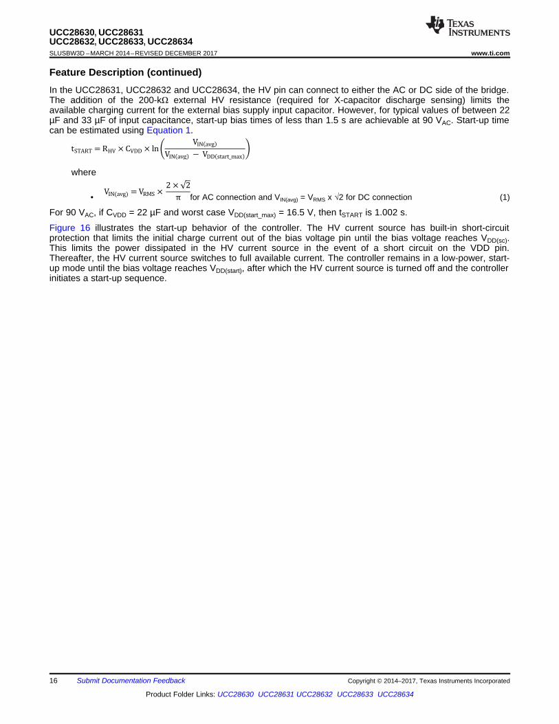
Feature Description (continued)In the UCC28631, UCC28632 and UCC28634, the HV pin can connect to either the AC or DC side of the bridge.The addition of the 200-kΩ external HV resistance (required for X-capacitor discharge sensing) limits theavailable charging current for the external bias supply input capacitor. However, for typical values of between 22µF and 33 µF of input capacitance, start-up bias times of less than 1.5 s are achievable at 90 VAC. Start-up timecan be estimated using Equation 1.
where
• for AC connection and VIN(avg) = VRMS x √2 for DC connection (1)
For 90 VAC, if CVDD = 22 µF and worst case VDD(start_max) = 16.5 V, then tSTART is 1.002 s.
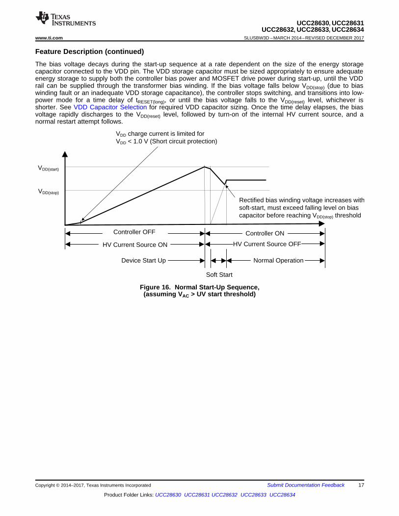
Figure 16 illustrates the start-up behavior of the controller. The HV current source has built-in short-circuitprotection that limits the initial charge current out of the bias voltage pin until the bias voltage reaches VDD(sc).This limits the power dissipated in the HV current source in the event of a short circuit on the VDD pin.Thereafter, the HV current source switches to full available current. The controller remains in a low-power, start-up mode until the bias voltage reaches VDD(start), after which the HV current source is turned off and the controllerinitiates a start-up sequence.
VDD(start)
Rectified bias winding voltage increases with soft-start, must exceed falling level on bias capacitor before reaching VDD(stop) threshold
VDD(stop)
VDD charge current is limited for VDD < 1.0 V (Short circuit protection)
Device Start Up
Soft Start
HV Current Source ON
Controller OFF Controller ON
Normal Operation
HV Current Source OFF
17
UCC28630, UCC28631UCC28632, UCC28633, UCC28634
www.ti.com SLUSBW3D –MARCH 2014–REVISED DECEMBER 2017
Product Folder Links: UCC28630 UCC28631 UCC28632 UCC28633 UCC28634
Submit Documentation FeedbackCopyright © 2014–2017, Texas Instruments Incorporated
Feature Description (continued)The bias voltage decays during the start-up sequence at a rate dependent on the size of the energy storagecapacitor connected to the VDD pin. The VDD storage capacitor must be sized appropriately to ensure adequateenergy storage to supply both the controller bias power and MOSFET drive power during start-up, until the VDDrail can be supplied through the transformer bias winding. If the bias voltage falls below VDD(stop) (due to biaswinding fault or an inadequate VDD storage capacitance), the controller stops switching, and transitions into low-power mode for a time delay of tRESET(long), or until the bias voltage falls to the VDD(reset) level, whichever isshorter. See VDD Capacitor Selection for required VDD capacitor sizing. Once the time delay elapses, the biasvoltage rapidly discharges to the VDD(reset) level, followed by turn-on of the internal HV current source, and anormal restart attempt follows.
Figure 16. Normal Start-Up Sequence,(assuming VAC > UV start threshold)
VAC rectified
VBULK
VDD
VDD(start)
VDD(stop)
VDD(reset)
DRV Terminal Line UV checkexploratory pulses
Normal PWM
VAC(on) threshold
tONUV(max) at fSW(uv)
Line UV checkexploratory pulses
Apply AC
tRESET(short)
Normal PWM soft-start
tONUV(max) at fSW(uv)
18
UCC28630, UCC28631UCC28632, UCC28633, UCC28634SLUSBW3D –MARCH 2014–REVISED DECEMBER 2017 www.ti.com
Product Folder Links: UCC28630 UCC28631 UCC28632 UCC28633 UCC28634
Submit Documentation Feedback Copyright © 2014–2017, Texas Instruments Incorporated
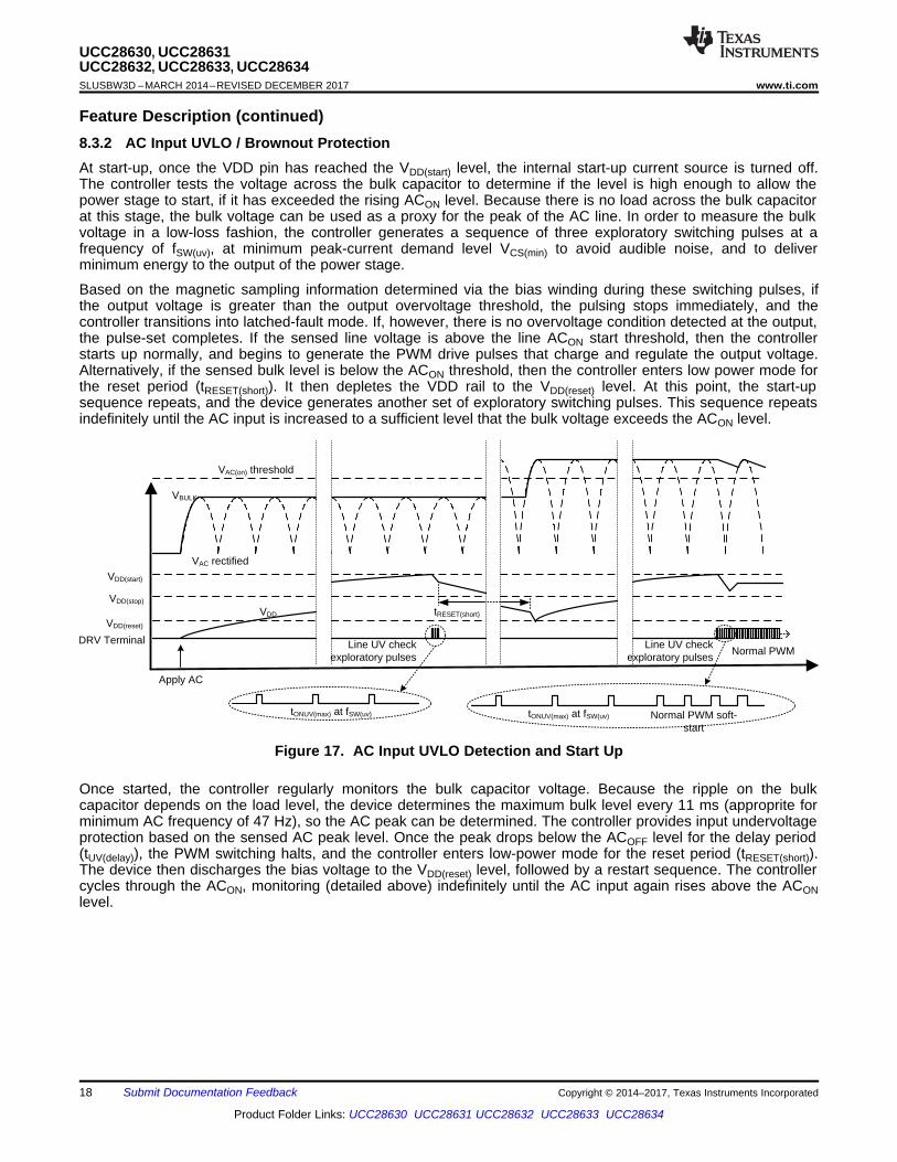
Feature Description (continued)8.3.2 AC Input UVLO / Brownout ProtectionAt start-up, once the VDD pin has reached the VDD(start) level, the internal start-up current source is turned off.The controller tests the voltage across the bulk capacitor to determine if the level is high enough to allow thepower stage to start, if it has exceeded the rising ACON level. Because there is no load across the bulk capacitorat this stage, the bulk voltage can be used as a proxy for the peak of the AC line. In order to measure the bulkvoltage in a low-loss fashion, the controller generates a sequence of three exploratory switching pulses at afrequency of fSW(uv), at minimum peak-current demand level VCS(min) to avoid audible noise, and to deliverminimum energy to the output of the power stage.
Based on the magnetic sampling information determined via the bias winding during these switching pulses, ifthe output voltage is greater than the output overvoltage threshold, the pulsing stops immediately, and thecontroller transitions into latched-fault mode. If, however, there is no overvoltage condition detected at the output,the pulse-set completes. If the sensed line voltage is above the line ACON start threshold, then the controllerstarts up normally, and begins to generate the PWM drive pulses that charge and regulate the output voltage.Alternatively, if the sensed bulk level is below the ACON threshold, then the controller enters low power mode forthe reset period (tRESET(short)). It then depletes the VDD rail to the VDD(reset) level. At this point, the start-upsequence repeats, and the device generates another set of exploratory switching pulses. This sequence repeatsindefinitely until the AC input is increased to a sufficient level that the bulk voltage exceeds the ACON level.
Figure 17. AC Input UVLO Detection and Start Up
Once started, the controller regularly monitors the bulk capacitor voltage. Because the ripple on the bulkcapacitor depends on the load level, the device determines the maximum bulk level every 11 ms (approprite forminimum AC frequency of 47 Hz), so the AC peak can be determined. The controller provides input undervoltageprotection based on the sensed AC peak level. Once the peak drops below the ACOFF level for the delay period(tUV(delay)), the PWM switching halts, and the controller enters low-power mode for the reset period (tRESET(short)).The device then discharges the bias voltage to the VDD(reset) level, followed by a restart sequence. The controllercycles through the ACON, monitoring (detailed above) indefinitely until the AC input again rises above the ACONlevel.
0
50
100
150
200
250
300
350
400
0 0.2 0.4 0.6 0.8 1 1.2 1.4 1.6 1.8 2 2.2 2.4
Vrm
s (V
)
Time (s)
V_SELV
Xcap_90
Xcap_115
Xcap_230
Xcap_264
C016
PX = VAC
2 × CX
19
UCC28630, UCC28631UCC28632, UCC28633, UCC28634
www.ti.com SLUSBW3D –MARCH 2014–REVISED DECEMBER 2017
Product Folder Links: UCC28630 UCC28631 UCC28632 UCC28633 UCC28634
Submit Documentation FeedbackCopyright © 2014–2017, Texas Instruments Incorporated
Feature Description (continued)8.3.3 Active X-Capacitor Discharge (UCC28630 and UCC28633 only)Safety standards such as EN60950 require that any X-capacitors in EMC filters on the AC side of the bridgerectifier quickly discharge to a safe level when AC is disconnected. This discharge requirement ensures that anyhigh-voltage level present at the pins of the AC plug does not present an electric shock hazard. The standardsrequire that the voltage across the X-capacitor decay with a maximum time constant of 1 second. Typically, thisrequirement is achieved by including a resistive discharge element in parallel with the X-capacitor. However, thisresistance causes a continuous power dissipation that impacts the standby power performance. The powerdissipation in the discharge resistors depends on the X-capacitor value. Assuming that the discharge resistormeets the 1-second time-constant requirement, (in other words, the R-C product is 1 second) the dissipation isdescribed in Equation 2.
(2)
Thus at 230 VAC, the discharge resistor causes 5.3-mW dissipation for every 100 nF of X-capacitance – for atypical 470-nF X-capacitor value, that causes 25 mW to be lost in the discharge resistors.
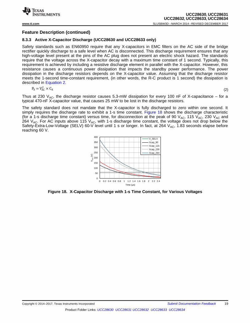
The safety standard does not mandate that the X-capacitor is fully discharged to zero within one second. Itsimply requires the discharge rate to exhibit a 1-s time constant. Figure 18 shows the discharge characteristic(for a 1-s discharge time constant) versus time, for disconnection at the peak of 90 VAC, 115 VAC, 230 VAC and264 VAC. For AC inputs above 115 VAC, with 1-s discharge time constant, the voltage does not drop below theSafety-Extra-Low-Voltage (SELV) 60-V level until 1 s or longer. In fact, at 264 VAC, 1.83 seconds elapse beforereaching 60 V.
Figure 18. X-Capacitor Discharge with 1-s Time Constant, for Various Voltages
CBULK Q2 lPNOM × PLL%
Dp×tXCAP(dis)
kVAC(pk)2 F VSELV
2o
CVDD R 330 nF × :48.15; = 15.9 JF
CVDD R CX ×F VAC:pk; FVSELV
VDD:start _min ; FVDD:reset _max ;G = CX × l373F 60
13.0F 6.5p = CX × (48.15)
20
UCC28630, UCC28631UCC28632, UCC28633, UCC28634SLUSBW3D –MARCH 2014–REVISED DECEMBER 2017 www.ti.com
Product Folder Links: UCC28630 UCC28631 UCC28632 UCC28633 UCC28634
Submit Documentation Feedback Copyright © 2014–2017, Texas Instruments Incorporated
Feature Description (continued)8.3.3.1 Improved Performance with UCC28630 and UCC28633In order to reduce standby power and eliminate the standing loss associated with the conventional dischargeresistors, the UCC28630 and the UCC28633 devices incorporate active X-capacitor discharge circuitry. Thiscircuit periodically monitors the voltage across the X-capacitor to detect any possible DC-condition (which wouldindicate that AC mains disconnection has occurred), and then discharges the voltage across the X-capacitorusing the internal HV current source. The X-capacitor discharge function discharges the X-capacitor to the SELV60-V level in 1 s (as long as the design considerations discussed in this section are followed).
The device internally monitors the current into the HV pin to determine if the voltage across the X-capacitor in theEMI filter has a sufficient AC ripple component. If insufficient AC content is detected, then a DC condition isinternally flagged. This causes the controller to enter low-power mode for the reset period (tRESET(short)), followedby bias voltage discharge to the reset level (VDD(reset)) , and then the start-up HV current source turns on again toeffectively discharge the X-capacitor by transferring charge to the VDD reservoir capacitor.
Because the device monitors the HV pin to detect a DC condition on the X-capacitor, the system cannot operatewith DC input to the HV pin. Instead, the HV pin must be connected to an AC source only. The device interpretsany DC input on the HV pin as DC across the X-capacitor, indicating an AC-disconnect event. This causes arepeating cycle of start-up and shutdown. The device requires an external 200-kΩ of resistance on the HV pin, tolimit the current to a level below the saturation point of the internal HV current source. This limit produces a HVinput current that is approximately proportional to AC line, so that the AC content can be sensed.
The size of the X-capacitor that can be discharged depends on the VDD energy storage capacitor. Assuming theworst case, a maximum X-capacitor disconnect voltage could be at the peak of 264 VRMS, and assuming that itshould be discharged down to 60-V SELV level, the minimum allowed VDD capacitor can be sized based on theworst case VDD(reset) and VDD(start) levels as described in Equation 3.
(3)
For example, for a 330-nF X-capacitor value, the required VDD capacitor is 15.9 µF, so a 22-µF capacitorsuffices.
(4)
In order to reduce the power consumption from the high voltage AC line, the device pulses current into the HVpin at a low frequency with very low duty-cycle. The HV current source on-time (tON(HV)) , repeats at intervals oftSMP(HV). Moreover, the pulsing occurs in bursts, with a time delay between bursts. The sampling occurs in burstsof 21, at intervals of tSMP(HV), with a wait time of tWAIT(HV) between bursts. This reduces the effective average duty-cycle to a very low value (approximately 0.2%), and minimizes the overhead of X-capacitor sampling current anddevice bias consumption overhead to approximately 2 mW of extra standby consumption at high-line 230 VAC.
The device enables the X-capacitor monitor in latched fault mode, and in light-load regions where the power levelis below PLL(%), as a percentage of the nominal rated level. Above the PLL(%) level, the X-capacitor monitor isdisabled. At this load level the bulk capacitor discharges at a rate that is sufficient to also discharge the X-capacitor, which appears in parallel with the bulk capacitor once the bulk voltage drops far enough to forwardbias the bridge rectifier diodes. In this case ensure that the bulk capacitance value is not too large for the powerlevel desired, which in-turn ensures that the bulk capacitor discharge rate is fast enough to discharge the X-capacitor to meet the 1-s discharge target. This can be calculated in Equation 5.
(5)
CBULK Q2 × l:65 × 0.125;
0.87p × 0.04
:2 × 652 F 602;LswvJF
2SELV
2OFF
delayUVLL%NOM
BULKVAC2
t
PP2
Cu
u¸¹
ᬩ
§ uu
d
CBULK Q2 × d:65 × 0.125;
0.87h × 1
:3732 F 602;LsuzJF
21
UCC28630, UCC28631UCC28632, UCC28633, UCC28634
www.ti.com SLUSBW3D –MARCH 2014–REVISED DECEMBER 2017
Product Folder Links: UCC28630 UCC28631 UCC28632 UCC28633 UCC28634
Submit Documentation FeedbackCopyright © 2014–2017, Texas Instruments Incorporated
Feature Description (continued)Assuming a worst case AC disconnect at the peak at 264 VRMS (373 VPK), and a requirement to discharge toSELV level of 60 V in tXCAP(dis) of 1 s, for a PNOM of 65 W at 87% efficiency, this is calculated in Equation 6.
(6)
Once the bulk capacitance value is chosen, also ensure that when the bulk capacitor has been discharged downto the line UV ACOFF threshold, that it continues to discharge to an acceptable level during the line UVpersistence delay time (tUV(delay)) as shown in Equation 7.
(7)
Again, taking the example above:
(8)
Once the first constraint is satisfied, the second one is also automatically met.
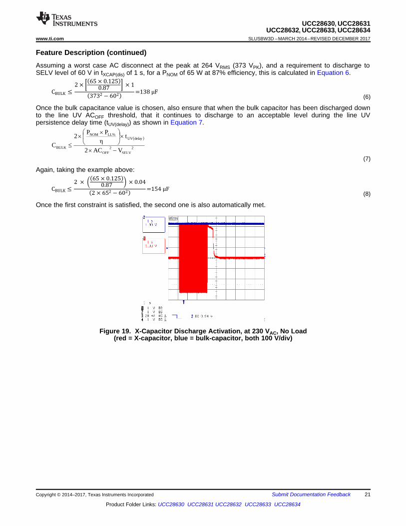
Figure 19. X-Capacitor Discharge Activation, at 230 VAC, No Load(red = X-capacitor, blue = bulk-capacitor, both 100 V/div)
22
UCC28630, UCC28631UCC28632, UCC28633, UCC28634SLUSBW3D –MARCH 2014–REVISED DECEMBER 2017 www.ti.com
Product Folder Links: UCC28630 UCC28631 UCC28632 UCC28633 UCC28634
Submit Documentation Feedback Copyright © 2014–2017, Texas Instruments Incorporated
Feature Description (continued)
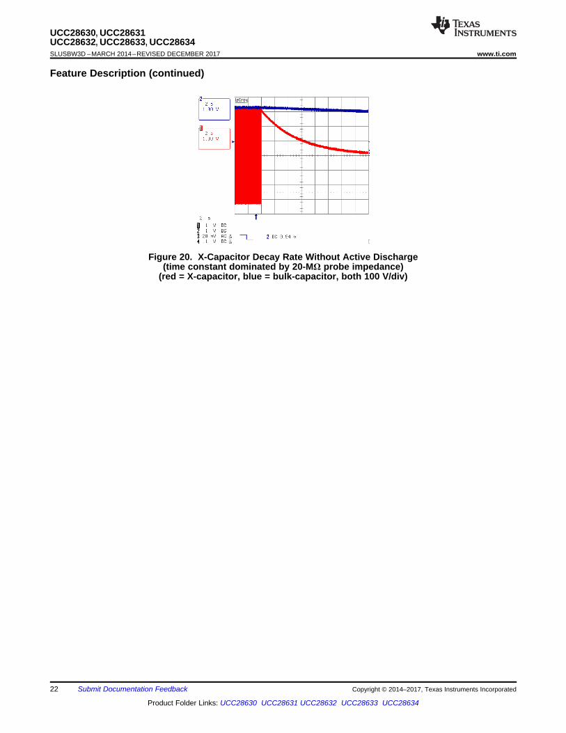
Figure 20. X-Capacitor Decay Rate Without Active Discharge(time constant dominated by 20-MΩ probe impedance)
(red = X-capacitor, blue = bulk-capacitor, both 100 V/div)
GNDRA
RB
VSENSE = VO x K1NBVO x K1
VIN x (NB/NP)
VO x (NB/NS)
NB
RB
RA RP
VF
DRV5
1 VSENSE
23
UCC28630, UCC28631UCC28632, UCC28633, UCC28634
www.ti.com SLUSBW3D –MARCH 2014–REVISED DECEMBER 2017
Product Folder Links: UCC28630 UCC28631 UCC28632 UCC28633 UCC28634
Submit Documentation FeedbackCopyright © 2014–2017, Texas Instruments Incorporated
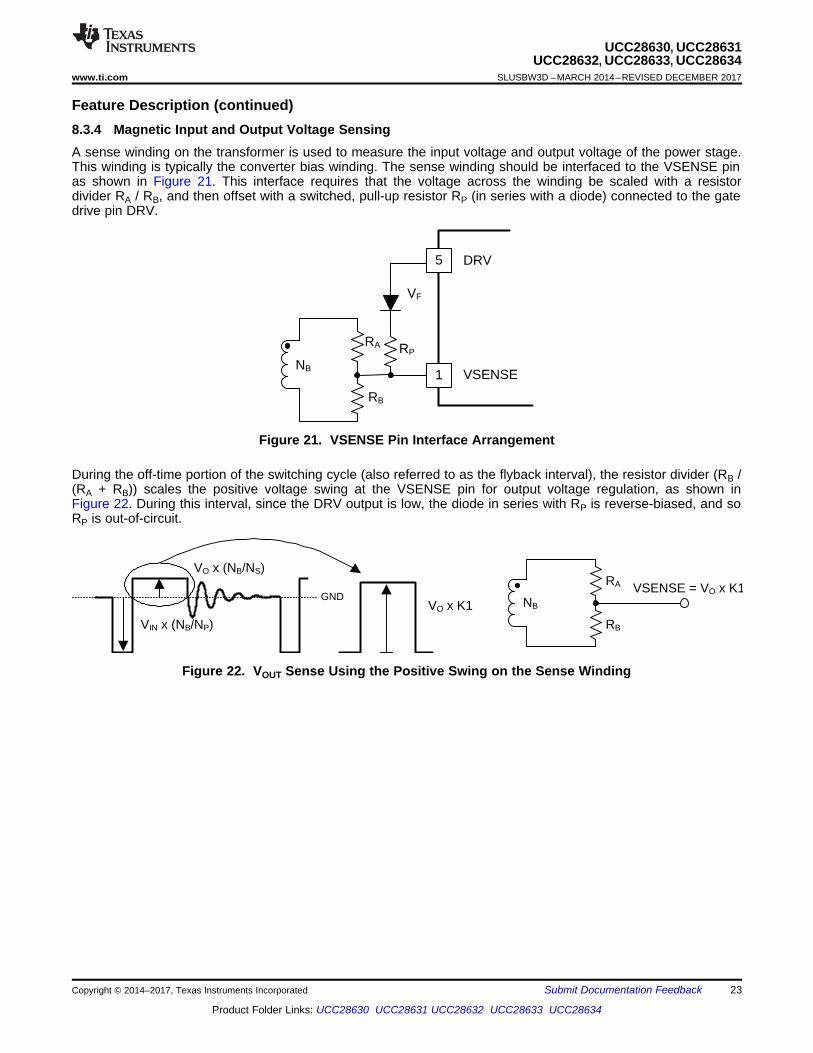
Feature Description (continued)8.3.4 Magnetic Input and Output Voltage SensingA sense winding on the transformer is used to measure the input voltage and output voltage of the power stage.This winding is typically the converter bias winding. The sense winding should be interfaced to the VSENSE pinas shown in Figure 21. This interface requires that the voltage across the winding be scaled with a resistordivider RA / RB, and then offset with a switched, pull-up resistor RP (in series with a diode) connected to the gatedrive pin DRV.
Figure 21. VSENSE Pin Interface Arrangement
During the off-time portion of the switching cycle (also referred to as the flyback interval), the resistor divider (RB /(RA + RB)) scales the positive voltage swing at the VSENSE pin for output voltage regulation, as shown inFigure 22. During this interval, since the DRV output is low, the diode in series with RP is reverse-biased, and soRP is out-of-circuit.
Figure 22. VOUT Sense Using the Positive Swing on the Sense Winding
NB
BAV70
SD
GND
VSENSE
CS
HV
VDD
DRV
UCC28630
1
2
3
4
8
6
5
RP
100 RA
RB
GNDRA
RB
VVSENSE = VDRV ± VF ± VIN x K2
NB
VIN x (NB/NP)
VO x (NB/NS)RP
VF
VDRV ± VF ± VIN x K2
DRV5
24
UCC28630, UCC28631UCC28632, UCC28633, UCC28634SLUSBW3D –MARCH 2014–REVISED DECEMBER 2017 www.ti.com
Product Folder Links: UCC28630 UCC28631 UCC28632 UCC28633 UCC28634
Submit Documentation Feedback Copyright © 2014–2017, Texas Instruments Incorporated
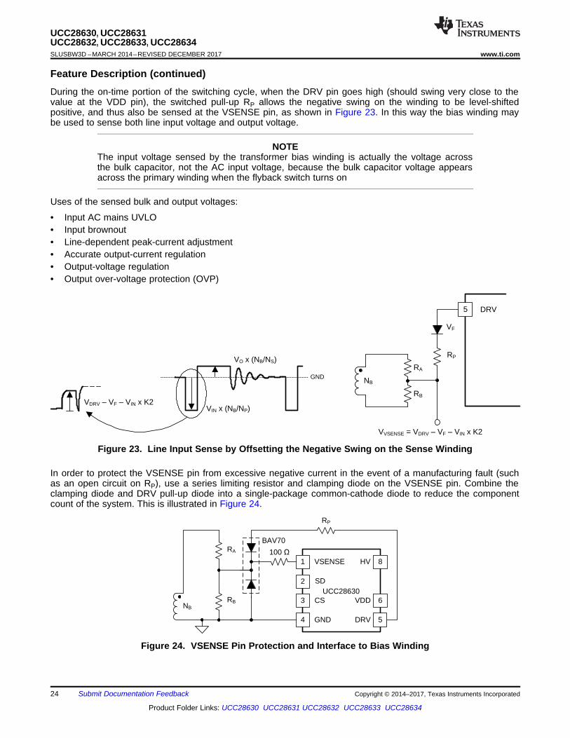
Feature Description (continued)During the on-time portion of the switching cycle, when the DRV pin goes high (should swing very close to thevalue at the VDD pin), the switched pull-up RP allows the negative swing on the winding to be level-shiftedpositive, and thus also be sensed at the VSENSE pin, as shown in Figure 23. In this way the bias winding maybe used to sense both line input voltage and output voltage.
NOTEThe input voltage sensed by the transformer bias winding is actually the voltage acrossthe bulk capacitor, not the AC input voltage, because the bulk capacitor voltage appearsacross the primary winding when the flyback switch turns on
Uses of the sensed bulk and output voltages:
• Input AC mains UVLO• Input brownout• Line-dependent peak-current adjustment• Accurate output-current regulation• Output-voltage regulation• Output over-voltage protection (OVP)
Figure 23. Line Input Sense by Offsetting the Negative Swing on the Sense Winding
In order to protect the VSENSE pin from excessive negative current in the event of a manufacturing fault (suchas an open circuit on RP), use a series limiting resistor and clamping diode on the VSENSE pin. Combine theclamping diode and DRV pull-up diode into a single-package common-cathode diode to reduce the componentcount of the system. This is illustrated in Figure 24.
Figure 24. VSENSE Pin Protection and Interface to Bias Winding
IPK(dem)
Gate turn-off delay
Current Sense
PWM Comparator
PWM drive
FET Gate
Bias Winding
VO sample delay
Time
25
UCC28630, UCC28631UCC28632, UCC28633, UCC28634
www.ti.com SLUSBW3D –MARCH 2014–REVISED DECEMBER 2017
Product Folder Links: UCC28630 UCC28631 UCC28632 UCC28633 UCC28634
Submit Documentation FeedbackCopyright © 2014–2017, Texas Instruments Incorporated
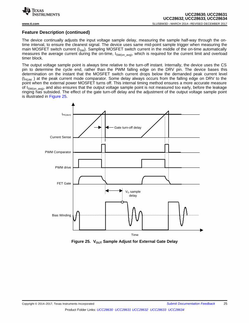
Feature Description (continued)The device continually adjusts the input voltage sample delay, measuring the sample half-way through the on-time interval, to ensure the cleanest signal. The device uses same mid-point sample trigger when measuring themain MOSFET switch current (ISW). Sampling MOSFET switch current in the middle of the on-time automaticallymeasures the average current during the on-time, ISW(on_avg), which is required for the current limit and overloadtimer block.
The output voltage sample point is always time relative to the turn-off instant. Internally, the device uses the CSpin to determine the cycle end, rather than the PWM falling edge on the DRV pin. The device bases thisdetermination on the instant that the MOSFET switch current drops below the demanded peak current level(IPEAK ) at the peak current mode comparator. Some delay always occurs from the falling edge on DRV to thepoint when the external power MOSFET turns off. This internal timing method ensures a more accurate measureof ISW(on_avg), and also ensures that the output voltage sample point is not measured too early, before the leakageringing has subsided. The effect of the gate turn-off delay and the adjustment of the output voltage sample pointis illustrated in Figure 25.
Figure 25. VOUT Sample Adjust for External Gate Delay
DRV
VIN Sample
VO sample
VIN sample delay
VO sample delay
Sense Winding
Primary Current
Secondary Current
Time
26
UCC28630, UCC28631UCC28632, UCC28633, UCC28634SLUSBW3D –MARCH 2014–REVISED DECEMBER 2017 www.ti.com
Product Folder Links: UCC28630 UCC28631 UCC28632 UCC28633 UCC28634
Submit Documentation Feedback Copyright © 2014–2017, Texas Instruments Incorporated
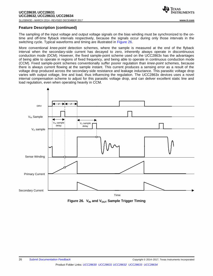
Feature Description (continued)The sampling of the input voltage and output voltage signals on the bias winding must be synchronized to the on-time and off-time flyback intervals respectively, because the signals occur during only those intervals in theswitching cycle. Typical waveforms and timing are illustrated in Figure 26.
More conventional knee-point detection schemes, where the sample is measured at the end of the flybackinterval when the secondary-side current has decayed to zero, inherently always operate in discontinuousconduction mode (DCM). However, the fixed sample-point scheme used on the UCC2863x has the advantagesof being able to operate in regions of fixed frequency, and being able to operate in continuous conduction mode(CCM). Fixed sample-point schemes conventionally suffer poorer regulation than knee-point schemes, becausethere is always current flowing at the sample instant. This current produces a sensing error as a result of thevoltage drop produced across the secondary-side resistance and leakage inductance. This parasitic voltage dropvaries with output voltage, line and load, thus influencing the regulation. The UCC2863x devices uses a novelinternal compensation scheme to adjust for this parasitic voltage drop, and can deliver excellent static line andload regulation, even when operating heavily in CCM.
Figure 26. VIN and VOUT Sample Trigger Timing
VO
RC(esr)
RSEC
VSEC
+
-
ISEC
+
+
++
-
-
-
-
+
-COUT
+
-LLEAK(sec_bias)
VRECT
VLEAK
VR(sec)
VBIAS
ILOAD
VRC(esr)
VSEC = VOUT × l1F LLK(sec bias )
LSEC
p + VRECT + ISEC × kRSEC + RC:esr;o F kILOAD × RC:esr;o
VSEC = VOUT + VRECT + VR(sec) FVL:leak; + VRC:esr;
27
UCC28630, UCC28631UCC28632, UCC28633, UCC28634
www.ti.com SLUSBW3D –MARCH 2014–REVISED DECEMBER 2017
Product Folder Links: UCC28630 UCC28631 UCC28632 UCC28633 UCC28634
Submit Documentation FeedbackCopyright © 2014–2017, Texas Instruments Incorporated
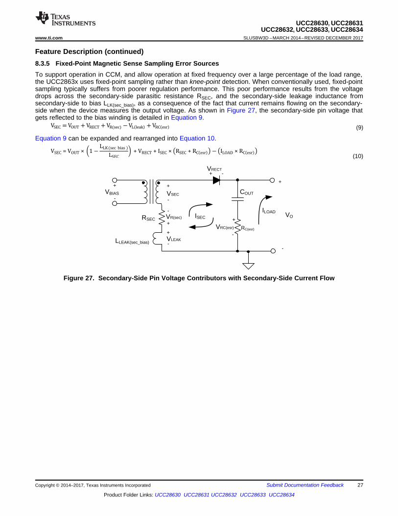
Feature Description (continued)8.3.5 Fixed-Point Magnetic Sense Sampling Error SourcesTo support operation in CCM, and allow operation at fixed frequency over a large percentage of the load range,the UCC2863x uses fixed-point sampling rather than knee-point detection. When conventionally used, fixed-pointsampling typically suffers from poorer regulation performance. This poor performance results from the voltagedrops across the secondary-side parasitic resistance RSEC, and the secondary-side leakage inductance fromsecondary-side to bias LLK(sec_bias), as a consequence of the fact that current remains flowing on the secondary-side when the device measures the output voltage. As shown in Figure 27, the secondary-side pin voltage thatgets reflected to the bias winding is detailed in Equation 9.
(9)
Equation 9 can be expanded and rearranged into Equation 10.
(10)
Figure 27. Secondary-Side Pin Voltage Contributors with Secondary-Side Current Flow
28
UCC28630, UCC28631UCC28632, UCC28633, UCC28634SLUSBW3D –MARCH 2014–REVISED DECEMBER 2017 www.ti.com
Product Folder Links: UCC28630 UCC28631 UCC28632 UCC28633 UCC28634
Submit Documentation Feedback Copyright © 2014–2017, Texas Instruments Incorporated
Feature Description (continued)Many elements contribute errors to the sensed secondary-side pin voltage, when measured across the biaswinding:• VL(leak): Negative voltage drop across the sec-bias leakage inductance LLK(sec_bias); assuming constant
regulated output voltage, this voltage drop is fixed constant offset, because VOUT/LSEC is constant as long asthe output is in regulation.
• VRECT: Positive voltage drop across the output rectifier (assuming use of a conventional diode). This voltagedrop varies with load current and temperature. However, a constant nominal voltage drop can usually beused, because the increasing forward voltage drop with increasing load current is largely cancelled by thedecrease in forward drop as a result of the temperature rise that results.
• VR(sec): This is the drop across the secondary-side winding resistance. This value depends on loading, andvaries in proportion to the primary peak current demand that is set by the modulator.
• VRC(esr): This is the drop across the output capacitor equivalent series resistance (esr). This value depends onthe difference between the secondary-side winding current and the DC load current being drawn.
Typically, the peak secondary-side winding current ISEC is many times larger than the load current, and thesecondary-side winding resistance is typically larger than the output capacitor esr. Thus, the last term inEquation 10 involving ILOAD can typically be neglected.
The leakage inductance and secondary-side rectifier terms represent quasi-constant offset terms, so do notaffect regulation to a significant extent. Thus, the quasi-constant offset terms can be accounted for in thecalculation of the required scaling resistors to produce the desired setpoint voltage.
The remaining term that dominates the regulation error in Equation 10 is the drop across the secondary-sidewinding resistance and capacitor esr at the sample instant, ISEC x(RSEC + RC(esr)). The controller internallyadjusts the control loop reference in proportion to the primary peak current demand in order to null the ISECrelated error term in the sampled bias winding voltage. Since the peak secondary-side current ISEC(pk) is theprimary peak current IPRI(pk) scaled by the transformer turns ratio, the internal control loop reference effectivelyvaries in approximate proportion to ISEC, resulting in dramatically improved regulation performance.
This improved regulation performance allows the use of primary-side regulation in a wider range of applications,and at unprecedented power levels, operating in both CCM and DCM.
RA = RP × lNB
NP
p × KLINE
NB
RA RP
RB1
VF
RB2
DRV5
1 VSENSE
29
UCC28630, UCC28631UCC28632, UCC28633, UCC28634
www.ti.com SLUSBW3D –MARCH 2014–REVISED DECEMBER 2017
Product Folder Links: UCC28630 UCC28631 UCC28632 UCC28633 UCC28634
Submit Documentation FeedbackCopyright © 2014–2017, Texas Instruments Incorporated
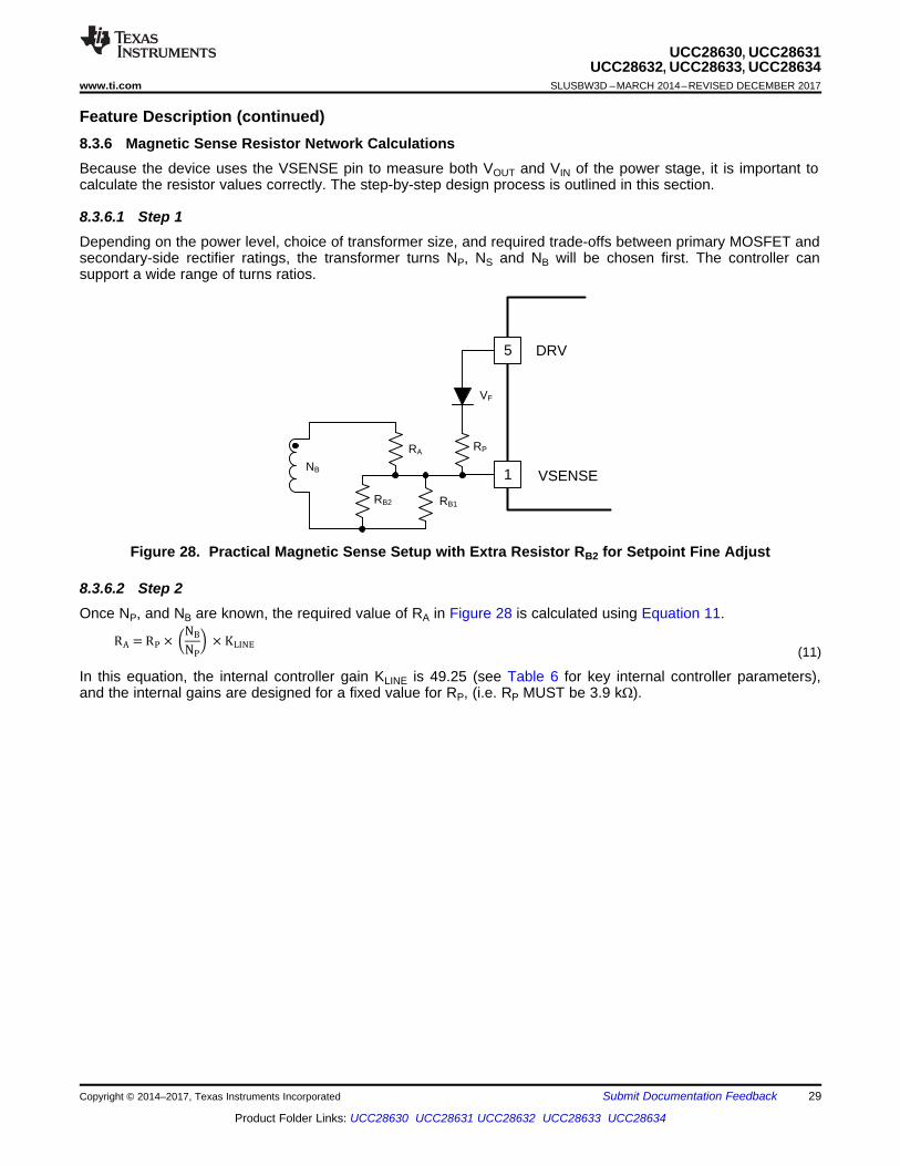
Feature Description (continued)8.3.6 Magnetic Sense Resistor Network CalculationsBecause the device uses the VSENSE pin to measure both VOUT and VIN of the power stage, it is important tocalculate the resistor values correctly. The step-by-step design process is outlined in this section.
8.3.6.1 Step 1Depending on the power level, choice of transformer size, and required trade-offs between primary MOSFET andsecondary-side rectifier ratings, the transformer turns NP, NS and NB will be chosen first. The controller cansupport a wide range of turns ratios.
Figure 28. Practical Magnetic Sense Setup with Extra Resistor RB2 for Setpoint Fine Adjust
8.3.6.2 Step 2Once NP, and NB are known, the required value of RA in Figure 28 is calculated using Equation 11.
(11)
In this equation, the internal controller gain KLINE is 49.25 (see Table 6 for key internal controller parameters),and the internal gains are designed for a fixed value for RP, (i.e. RP MUST be 3.9 kΩ).
10 k3ORTH < 20 k3
RTH = RA × RB
RA + RB
RB = RA
LkVOUT × k1F%LLK:sec _bias ;o + VRECTo × @NB
NSA
VOUT:ref ; F 1M
30
UCC28630, UCC28631UCC28632, UCC28633, UCC28634SLUSBW3D –MARCH 2014–REVISED DECEMBER 2017 www.ti.com
Product Folder Links: UCC28630 UCC28631 UCC28632 UCC28633 UCC28634
Submit Documentation Feedback Copyright © 2014–2017, Texas Instruments Incorporated
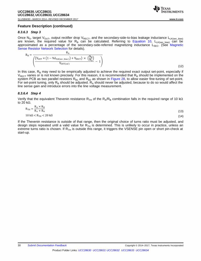
Feature Description (continued)8.3.6.3 Step 3Once NS, target VOUT, output rectifier drop VRECT, and the secondary-side-to-bias leakage inductance LLK(sec_bias)are known, the required value for RB can be calculated. Referring to Equation 10, LLK(sec_bias) can beapproximated as a percentage of the secondary-side-referred magnetizing inductance LSEC. (See MagneticSense Resistor Network Selection for details).
(12)
In this case, RB may need to be empirically adjusted to achieve the required exact output set-point, especially ifVRECT varies or is not known precisely. For this reason, it is recommended that RB should be implemented on thesystem PCB as two parallel resistors RB1 and RB2 as shown in Figure 28, to allow easier fine-tuning of set-point.For set-point tuning, only RB should be adjusted. RA should never be adjusted, because to do so would affect theline sense gain and introduce errors into the line voltage measurement.
8.3.6.4 Step 4Verify that the equivalent Thevenin resistance RTH of the RA/RB combination falls in the required range of 10 kΩto 20 kΩ.
(13)
(14)
If the Thevenin resistance is outside of that range, then the original choice of turns ratio must be adjusted, anddesign steps repeated until a valid value for RTH is determined. This is unlikely to occur in practice, unless anextreme turns ratio is chosen. If RTH is outside this range, it triggers the VSENSE pin open or short pin-check atstart-up.
RCS
LPRI
Q1
VIN:pk _max ; ×
VCS:min ;
tON:min ;
RCS
LPRI
QVCS:min ;
tOUT:smp ; ×
NS
NP
× 1
:VOUT + VRECT;
31
UCC28630, UCC28631UCC28632, UCC28633, UCC28634
www.ti.com SLUSBW3D –MARCH 2014–REVISED DECEMBER 2017
Product Folder Links: UCC28630 UCC28631 UCC28632 UCC28633 UCC28634
Submit Documentation FeedbackCopyright © 2014–2017, Texas Instruments Incorporated
Feature Description (continued)8.3.7 Magnetic Sensing: Power Stage Design ConstraintsBecause the controller employs fixed-point sampling for output voltage sensing, there are some transformerdesign constraints that must be observed. The minimum magnetizing volt-seconds during the on-time intervaloccurs at the minimum CS pin voltage, VCS(min), under light-load conditions. This minimum should be the case atall line voltages, because the controller compensates for line-dependent peak-current overshoot during turn-offdelay. The choice of transformer turns ratio, transformer inductance (LPRI), and current sense resistance (RCS)must ensure that the corresponding reset volt-seconds during the flyback interval are sufficient that a valid outputsample is available at the sample point, tOUT(smp). This constraint is summarized in Equation 15.
where• VRECT is the voltage drop across the output rectifier (15)
Additionally, the device requires a minimum on-time, tON(min) , to ensure enough time for the system input voltage(VIN) and switch current (ISW ) to be measured. To meet the minimum on-time requirement at maximum line, andminimum load, the ratio of current sense resistance (RCS) to transformer inductance (LPRI) must meet theconstraint shown in Equation 16.
(16)
Equation 15 or Equation 16 sets the limit for the ratio of RCS to LPRI, but both need to be verified. See TypicalApplication for more details.
VO Sample
VREF(adj)
Voltage Loop PID Compensator
VO
tSMP
VSENSE
VREF KR(sec) IPK(dem)
+
+
+
-Error ek Output yk
To fSW and IPK(dem) Modulator1
32
UCC28630, UCC28631UCC28632, UCC28633, UCC28634SLUSBW3D –MARCH 2014–REVISED DECEMBER 2017 www.ti.com
Product Folder Links: UCC28630 UCC28631 UCC28632 UCC28633 UCC28634
Submit Documentation Feedback Copyright © 2014–2017, Texas Instruments Incorporated
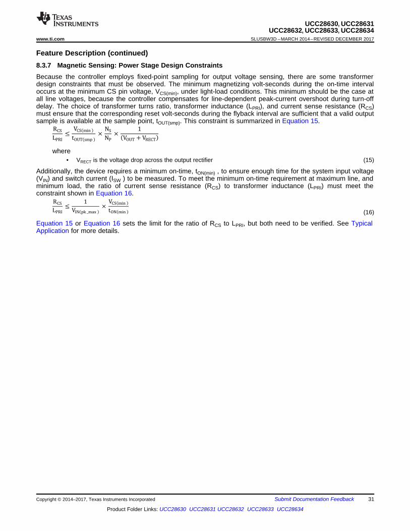
Feature Description (continued)8.3.8 Magnetic Sense Voltage Control LoopBecause the output voltage feedback is inherently a sampled signal obtained from the bias winding, the internalvoltage control loop is most naturally implemented digitally. The internal control loop implements the equivalentof a PID loop in digital form. Because the output can be sampled only at certain intervals in each switching cycle,the sample rate is naturally tied to the switching frequency, and the sample rate increases with increasingfrequency. However, the device clamps the sample rate at a normalized maximum rate, fSMP(max). But becausethe device must always synchronize to the next available switching cycle to obtain a new sample of the outputvoltage, the effective sample rate varies somewhat around this value.
The digital control loop compensator block diagram is shown in Figure 29. A new sample of output voltage issupplied to the compensator at the normalized maximum clock rate (fSMP(max)) , or fSW, whichever is lower. Anupdated output voltage demand signal, yk, is produced at the same clock rate. This voltage loop demandrepresents the required operating point on the modulator curves to keep the output voltage in regulation. Themodulator sets the appropriate switching frequency and peak current demand depending on the load power.
Figure 29. Digital Voltage Control Loop Simplified Block Diagram
The control loop PID gain factors are internally fixed values, optimized for flyback power stages in the rangebetween 20 W and 130 W. The loop is designed to work with magnetizing inductance values in the rangebetween 200 µH and 1500 µH. Assuming that the output capacitance value is chosen based on required ripplecurrent rating, then loop stability is not a problem. Adding extra output capacitance does not degrade the loopperformance and the resulting extra output hold-up improves transient response.
The Typical Application section includes gain-phase measurements taken using the 65-W UCC28630EVM-572evaluation module.
SD
GND
VSENSE
CS
HV
VDD
DRV
UCC28630
1
2
3
4
8
6
5
CCS
RCS2
RCS1
33
UCC28630, UCC28631UCC28632, UCC28633, UCC28634
www.ti.com SLUSBW3D –MARCH 2014–REVISED DECEMBER 2017
Product Folder Links: UCC28630 UCC28631 UCC28632 UCC28633 UCC28634
Submit Documentation FeedbackCopyright © 2014–2017, Texas Instruments Incorporated
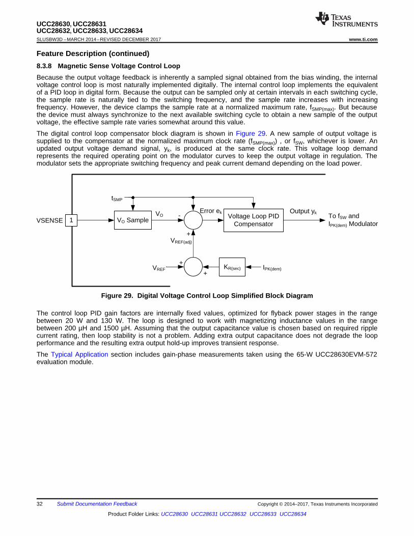
Feature Description (continued)8.3.9 Peak Current Mode ControlThe controller operates in peak current mode. The primary-side switch (MOSFET) current is sensed by a shuntresistor (RCS1) connected in series with the source of the FET as shown in Figure 30. The voltage that isdeveloped across the sense resistor is connected to the CS pin of the controller. The device uses the currentsense signal at the CS pin to terminate the PWM pulse according to the peak current demand of the modulator.The device automatically applies slope compensation as soon as the duty cycle of the DRV pin pulse exceeds50%. This compensation provides stable operation up to maximum DRV duty cycle. The device applies this slopecompensation as a downslope on the demand signal at the PWM comparator, so is not measureable at the CSpin. The device synchronizes the slope compensation signal to the PWM and is active only between 50% and70% duty cycle, as shown in Figure 31.
Normal operating range for the CS pin is between 0 mV and 800 mV. The RCS1 resistor should be scaled suchthat the peak current at maximum peak load and minimum bulk capacitor voltage produces a signal ofapproximately 800 mV peak at the CS pin. This resistor value is calculated in conjunction with the calculation ofthe required primary magnetizing inductance, as outlined in Notebook Adapter, 19.5 V, 65 W, section.
Figure 30. Primary-Side Current Sensing
Peak Current DemandWith Slope Compensation
PWM Clock at 60 kHz
100 mVPP
50% 70%
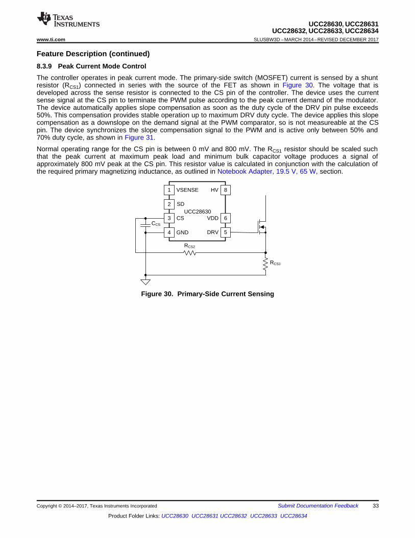
30 mV/s
34
UCC28630, UCC28631UCC28632, UCC28633, UCC28634SLUSBW3D –MARCH 2014–REVISED DECEMBER 2017 www.ti.com
Product Folder Links: UCC28630 UCC28631 UCC28632 UCC28633 UCC28634
Submit Documentation Feedback Copyright © 2014–2017, Texas Instruments Incorporated
Feature Description (continued)A nominal 100 ns of filtering that is internal to the CS pin helps filter the leading turn-on spike of current.Depending on PCB layout, an RC filter (RCS2 and CCS) may be required on the CS pin as shown in Figure 30 tofilter noise and spikes. The capacitor CCS should be positioned as close as possible to pins 3 and 4 and trackeddirectly to the pins. Series resistor RCS2 should also be located close to pin 3 to minimize noise pick-up. RCS2value should not exceed 20 kΩ, because a larger value could be detected as a possible open circuit on the CSpin during the start-up pin-fault checks. The R-C filter time constant should not be excessive (timing between 100ns and 200 ns is typical). Otherwise the filter reduces the measured peak current, and allows greater actual peakcurrent to flow versus the modulator demand level. Such effects force the regulation loop to reduce the switchingfrequency to compensate, and at highest line, no load, this can lead to regulation difficulties if the control loopattempts to drop the frequency so far that it reaches the fMIN limit.
Figure 31. Peak Current Demand with Slope Compensating Downslope
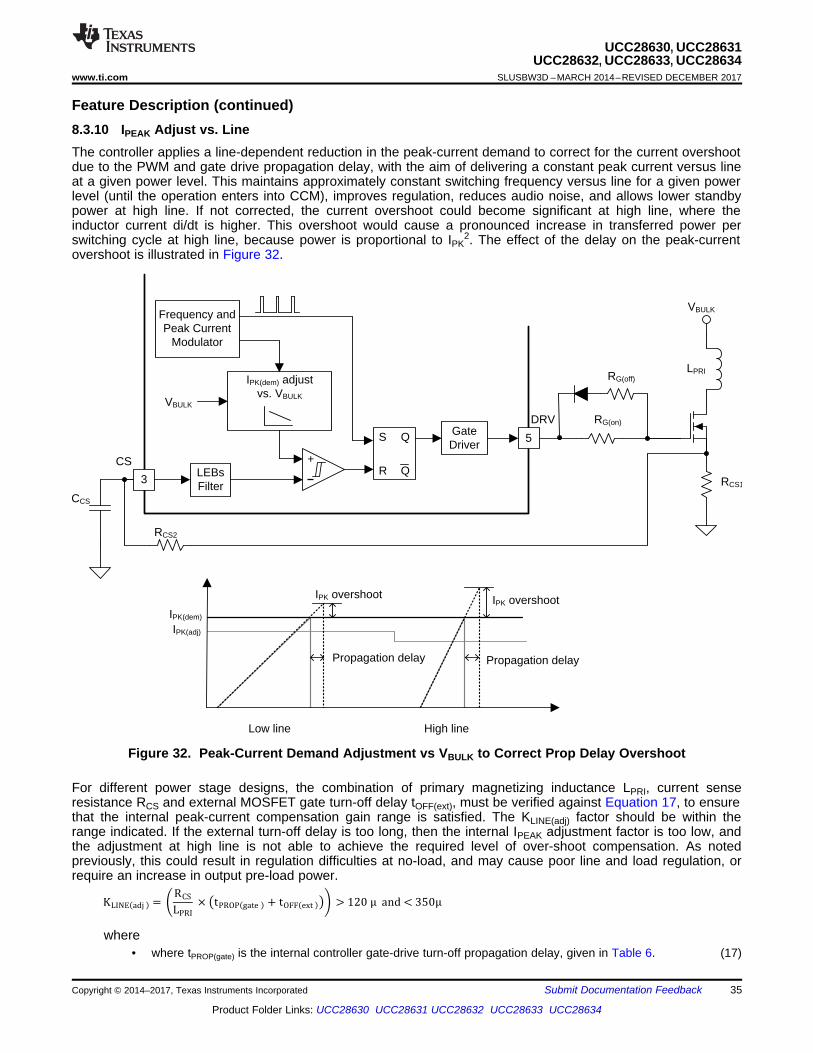
KLINE:adj ; = FRCS
LPRI
× ktPROP:gate ; + tOFF:ext ;oG PstrJand < uwrJ
+
S Q
QRLEBsFilter
Frequency andPeak Current
Modulator
IPK(dem) adjustvs. VBULK
CS
VBULK
Gate Driver
RG(on)
RG(off)
VBULK
LPRI
RCS1
RCS2
CCS
Low line High line
IPK(dem)
Propagation delay
IPK overshoot IPK overshoot
IPK(adj)
Propagation delay
DRV
5
3
35
UCC28630, UCC28631UCC28632, UCC28633, UCC28634
www.ti.com SLUSBW3D –MARCH 2014–REVISED DECEMBER 2017
Product Folder Links: UCC28630 UCC28631 UCC28632 UCC28633 UCC28634
Submit Documentation FeedbackCopyright © 2014–2017, Texas Instruments Incorporated
Feature Description (continued)8.3.10 IPEAK Adjust vs. LineThe controller applies a line-dependent reduction in the peak-current demand to correct for the current overshootdue to the PWM and gate drive propagation delay, with the aim of delivering a constant peak current versus lineat a given power level. This maintains approximately constant switching frequency versus line for a given powerlevel (until the operation enters into CCM), improves regulation, reduces audio noise, and allows lower standbypower at high line. If not corrected, the current overshoot could become significant at high line, where theinductor current di/dt is higher. This overshoot would cause a pronounced increase in transferred power perswitching cycle at high line, because power is proportional to IPK
2. The effect of the delay on the peak-currentovershoot is illustrated in Figure 32.
Figure 32. Peak-Current Demand Adjustment vs VBULK to Correct Prop Delay Overshoot
For different power stage designs, the combination of primary magnetizing inductance LPRI, current senseresistance RCS and external MOSFET gate turn-off delay tOFF(ext), must be verified against Equation 17, to ensurethat the internal peak-current compensation gain range is satisfied. The KLINE(adj) factor should be within therange indicated. If the external turn-off delay is too long, then the internal IPEAK adjustment factor is too low, andthe adjustment at high line is not able to achieve the required level of over-shoot compensation. As notedpreviously, this could result in regulation difficulties at no-load, and may cause poor line and load regulation, orrequire an increase in output pre-load power.
where• where tPROP(gate) is the internal controller gate-drive turn-off propagation delay, given in Table 6. (17)
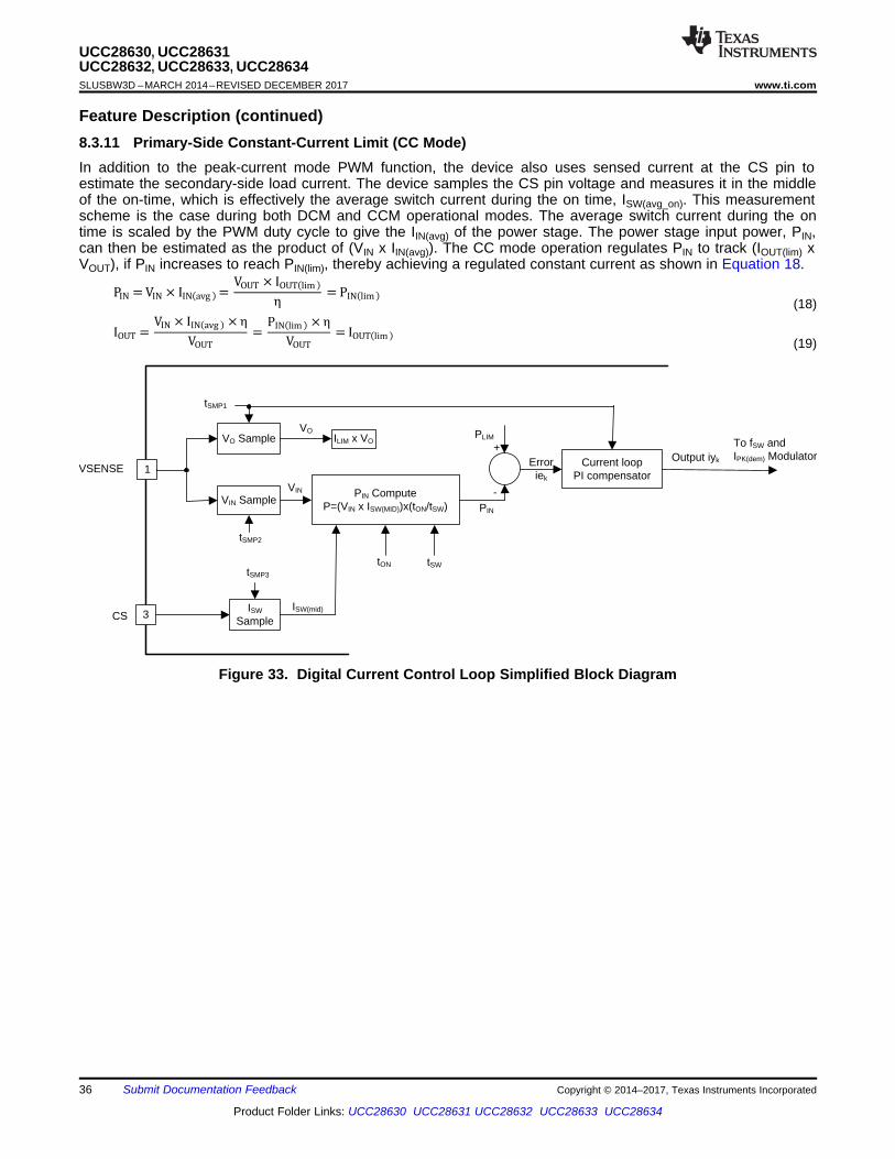
VSENSE
VO Sample
VIN SamplePIN Compute
P=(VIN x ISW(MID))x(tON/tSW)
VIN
tON tSW
VO
PIN
PLIMILIM x VO
tSMP1
tSMP2
+
-
Current loop PI compensator
Error iek
Output iyk
CSISW
SampleISW(mid)
tSMP3
To fSW and IPK(dem) Modulator
1
3
IOUT = VIN × IIN:avg ; × D
VOUT
= PIN:lim ; × D
VOUT
= IOUT:lim ;
PIN = VIN × IIN:avg ; = VOUT × IOUT:lim ;
D = PIN:lim ;
36
UCC28630, UCC28631UCC28632, UCC28633, UCC28634SLUSBW3D –MARCH 2014–REVISED DECEMBER 2017 www.ti.com
Product Folder Links: UCC28630 UCC28631 UCC28632 UCC28633 UCC28634
Submit Documentation Feedback Copyright © 2014–2017, Texas Instruments Incorporated
Feature Description (continued)8.3.11 Primary-Side Constant-Current Limit (CC Mode)In addition to the peak-current mode PWM function, the device also uses sensed current at the CS pin toestimate the secondary-side load current. The device samples the CS pin voltage and measures it in the middleof the on-time, which is effectively the average switch current during the on time, ISW(avg_on). This measurementscheme is the case during both DCM and CCM operational modes. The average switch current during the ontime is scaled by the PWM duty cycle to give the IIN(avg) of the power stage. The power stage input power, PIN,can then be estimated as the product of (VIN x IIN(avg)). The CC mode operation regulates PIN to track (IOUT(lim) xVOUT), if PIN increases to reach PIN(lim), thereby achieving a regulated constant current as shown in Equation 18.
(18)
(19)
Figure 33. Digital Current Control Loop Simplified Block Diagram
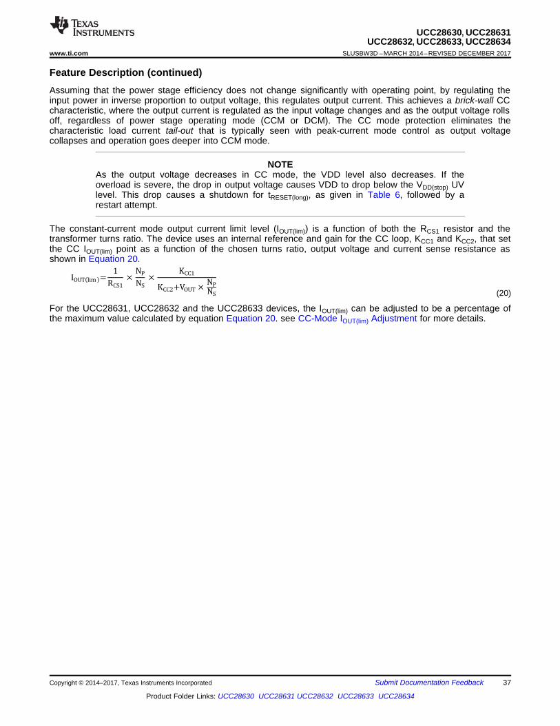
IOUT:lim ;=1
RCS1
× NP
NS
× KCC1
KCC2+VOUT × NP
NS
37
UCC28630, UCC28631UCC28632, UCC28633, UCC28634
www.ti.com SLUSBW3D –MARCH 2014–REVISED DECEMBER 2017
Product Folder Links: UCC28630 UCC28631 UCC28632 UCC28633 UCC28634
Submit Documentation FeedbackCopyright © 2014–2017, Texas Instruments Incorporated
Feature Description (continued)Assuming that the power stage efficiency does not change significantly with operating point, by regulating theinput power in inverse proportion to output voltage, this regulates output current. This achieves a brick-wall CCcharacteristic, where the output current is regulated as the input voltage changes and as the output voltage rollsoff, regardless of power stage operating mode (CCM or DCM). The CC mode protection eliminates thecharacteristic load current tail-out that is typically seen with peak-current mode control as output voltagecollapses and operation goes deeper into CCM mode.
NOTEAs the output voltage decreases in CC mode, the VDD level also decreases. If theoverload is severe, the drop in output voltage causes VDD to drop below the VDD(stop) UVlevel. This drop causes a shutdown for tRESET(long), as given in Table 6, followed by arestart attempt.
The constant-current mode output current limit level (IOUT(lim)) is a function of both the RCS1 resistor and thetransformer turns ratio. The device uses an internal reference and gain for the CC loop, KCC1 and KCC2, that setthe CC IOUT(lim) point as a function of the chosen turns ratio, output voltage and current sense resistance asshown in Equation 20.
(20)
For the UCC28631, UCC28632 and the UCC28633 devices, the IOUT(lim) can be adjusted to be a percentage ofthe maximum value calculated by equation Equation 20. see CC-Mode IOUT(lim) Adjustment for more details.

38
UCC28630, UCC28631UCC28632, UCC28633, UCC28634SLUSBW3D –MARCH 2014–REVISED DECEMBER 2017 www.ti.com
Product Folder Links: UCC28630 UCC28631 UCC28632 UCC28633 UCC28634
Submit Documentation Feedback Copyright © 2014–2017, Texas Instruments Incorporated
Feature Description (continued)8.3.12 Primary-Side Overload Timer (UCC28630 only)The internal overload timer in the UCC28630 uses the same output load current measurement that is used bythe CC loop. This measurement tracks the power stage thermal stress, and protects the power stage againstoutput overload. If the output is overloaded for too long such that the power stage would be over-stressed, thenthe PWM shuts down, and enters low-power mode for a time period of tRESET(long); thereafter the devicedischarges VDD to the VDD(reset) level and initiates a hiccup mode restart.
The overload timer operates by taking an estimate of output current, squaring it (assuming the power stagelosses are dominated by resistive I2 losses) to produce (K x I2OUT), where K is a scaling gain factor. The overloadtimer is constantly running at every load level, and accumulates at a rate dependent on the difference between(K x I2OUT) and the previous level of the timer. If (K x I2OUT) is greater than the previous timer level, the timer levelcontinues to increase; if (K x I2OUT) is less than the previous timer level, then the timer level decreases. At anysteady load, the overload timer level eventually settles at a level proportional to I2OUT. Because the overloadtimer level adjusts at a rate dependent on the difference between (K xI2OUT) and the previous level, the timerinitially reacts faster to larger differences, but over time settles exponentially at a level proportional to (K x I2OUT).
As shown in Figure 34, in both the first and second examples, the initial steady load allows the timer to integrateand settle at a level proportional to the load. The margin to the over-load trip level depends on the historicalloading, lower prior average loading results in greater future over-load capability, and vice versa. The rate atwhich the timer reacts to different load steps is set by the chosen time constant (or response rate) per Table 1.
The overload timer can cope with pulsed loads and loads with a complex waveform. Because the rate ofincrease and decrease also depends on the load change from the previous load, it also times out faster forbigger overloads, or allows a smaller overload to run for much longer. The overload timer operates in bothnormal CV mode and overload CC mode, or a dynamic mix of both modes.
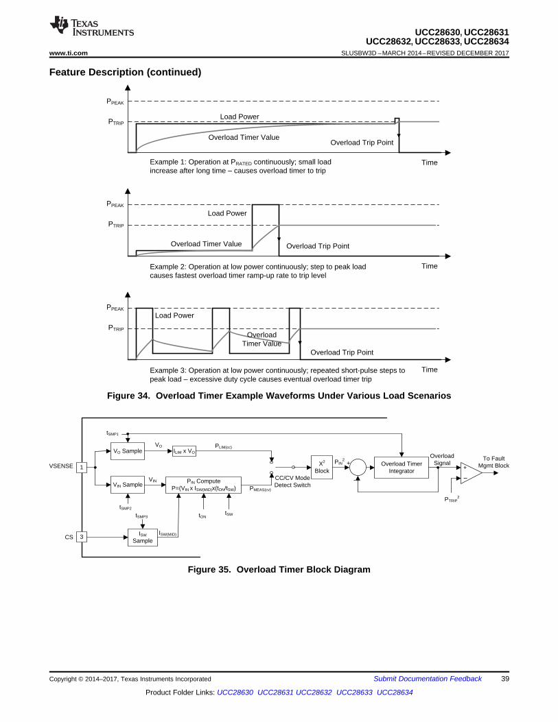
VO Sample
VIN SamplePIN Compute
P=(VIN x ISW(MID)x(tON/tSW)
VIN
tONtSW
VO
PMEAS(cv)
PLIM(cc)ILIM x VO
tSMP1
tSMP2
Overload Timer Integrator
PIN2
Overload Signal
To Fault Mgmt Block
CC/CV Mode Detect Switch
X2 Block
+
-
+
PTRIP2
CSISW
SampleISW(MID)
tSMP3
VSENSE 1
3
PPEAK
PTRIP
Time
Overload Trip Point
Example 1: Operation at PRATED continuously; small load increase after long time ± causes overload timer to trip
Time
Overload Trip Point
Example 2: Operation at low power continuously; step to peak load causes fastest overload timer ramp-up rate to trip level
PPEAK
PTRIP
Time
Overload Trip Point
Example 3: Operation at low power continuously; repeated short-pulse steps to peak load ± excessive duty cycle causes eventual overload timer trip
PPEAK
PTRIP
Load Power
Load Power
Load Power
Overload Timer Value
Overload Timer Value
Overload Timer Value
39
UCC28630, UCC28631UCC28632, UCC28633, UCC28634
www.ti.com SLUSBW3D –MARCH 2014–REVISED DECEMBER 2017
Product Folder Links: UCC28630 UCC28631 UCC28632 UCC28633 UCC28634
Submit Documentation FeedbackCopyright © 2014–2017, Texas Instruments Incorporated
Feature Description (continued)
Figure 34. Overload Timer Example Waveforms Under Various Load Scenarios
Figure 35. Overload Timer Block Diagram
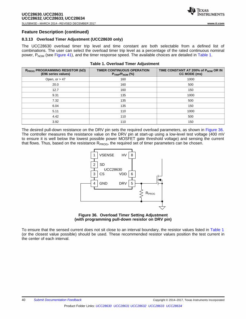
SD
GND
VSENSE
CS
HV
VDD
DRV
UCC28630
1
2
3
4
8
6
5
RPROG
40
UCC28630, UCC28631UCC28632, UCC28633, UCC28634SLUSBW3D –MARCH 2014–REVISED DECEMBER 2017 www.ti.com
Product Folder Links: UCC28630 UCC28631 UCC28632 UCC28633 UCC28634
Submit Documentation Feedback Copyright © 2014–2017, Texas Instruments Incorporated
Feature Description (continued)8.3.13 Overload Timer Adjustment (UCC28630 only)The UCC28630 overload timer trip level and time constant are both selectable from a defined list ofcombinations. The user can select the overload timer trip level as a percentage of the rated continuous nominalpower, PNOM (see Figure 41), and the timer response speed. The available choices are detailed in Table 1.
Table 1. Overload Timer AdjustmentRPROG PROGRAMMING RESISTOR (kΩ)
(E96 series values)TIMER CONTINUOUS OPERATION
PTRIP/PNOM (%)TIME CONSTANT AT 200% of PNOM OR IN
CC MODE (ms)Open, or > 47 160 1000
20.0 160 50012.7 160 1509.31 135 10007.32 135 5006.04 135 1505.11 110 10004.42 110 5003.92 110 150
The desired pull-down resistance on the DRV pin sets the required overload parameters, as shown in Figure 36.The controller measures the resistance value on the DRV pin at start-up using a low-level test voltage (400 mVto ensure it is well below the lowest possible power MOSFET gate threshold voltage) and sensing the currentthat flows. Thus, based on the resistance RPROG, the required set of timer parameters can be chosen.
Figure 36. Overload Timer Setting Adjustment(with programming pull-down resistor on DRV pin)
To ensure that the sensed current does not sit close to an interval boundary, the resistor values listed in Table 1(or the closest value possible) should be used. These recommended resistor values position the test current inthe center of each interval.
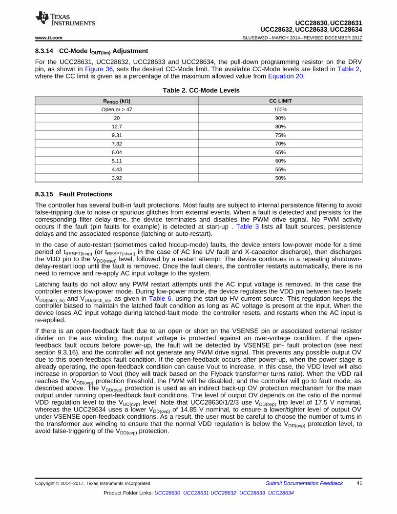
41
UCC28630, UCC28631UCC28632, UCC28633, UCC28634
www.ti.com SLUSBW3D –MARCH 2014–REVISED DECEMBER 2017
Product Folder Links: UCC28630 UCC28631 UCC28632 UCC28633 UCC28634
Submit Documentation FeedbackCopyright © 2014–2017, Texas Instruments Incorporated
8.3.14 CC-Mode IOUT(lim) AdjustmentFor the UCC28631, UCC28632, UCC28633 and UCC28634, the pull-down programming resistor on the DRVpin, as shown in Figure 36, sets the desired CC-Mode limit. The available CC-Mode levels are listed in Table 2,where the CC limit is given as a percentage of the maximum allowed value from Equation 20.
Table 2. CC-Mode LevelsRPROG (kΩ) CC LIMIT
Open or > 47 100%20 90%
12.7 80%9.31 75%7.32 70%6.04 65%5.11 60%4.43 55%3.92 50%
8.3.15 Fault ProtectionsThe controller has several built-in fault protections. Most faults are subject to internal persistence filtering to avoidfalse-tripping due to noise or spurious glitches from external events. When a fault is detected and persists for thecorresponding filter delay time, the device terminates and disables the PWM drive signal. No PWM activityoccurs if the fault (pin faults for example) is detected at start-up . Table 3 lists all fault sources, persistencedelays and the associated response (latching or auto-restart).
In the case of auto-restart (sometimes called hiccup-mode) faults, the device enters low-power mode for a timeperiod of tRESET(long) (or tRESET(short) in the case of AC line UV fault and X-capacitor discharge), then dischargesthe VDD pin to the VDD(reset) level, followed by a restart attempt. The device continues in a repeating shutdown-delay-restart loop until the fault is removed. Once the fault clears, the controller restarts automatically, there is noneed to remove and re-apply AC input voltage to the system.
Latching faults do not allow any PWM restart attempts until the AC input voltage is removed. In this case thecontroller enters low-power mode. During low-power mode, the device regulates the VDD pin between two levelsVDD(latch_hi) and VDD(latch_lo), as given in Table 6, using the start-up HV current source. This regulation keeps thecontroller biased to maintain the latched fault condition as long as AC voltage is present at the input. When thedevice loses AC input voltage during latched-fault mode, the controller resets, and restarts when the AC input isre-applied.
If there is an open-feedback fault due to an open or short on the VSENSE pin or associated external resistordivider on the aux winding, the output voltage is protected against an over-voltage condition. If the open-feedback fault occurs before power-up, the fault will be detected by VSENSE pin- fault protection (see nextsection 9.3.16), and the controller will not generate any PWM drive signal. This prevents any possible output OVdue to this open-feedback fault condition. If the open-feedback occurs after power-up, when the power stage isalready operating, the open-feedback condition can cause Vout to increase. In this case, the VDD level will alsoincrease in proportion to Vout (they will track based on the Flyback transformer turns ratio). When the VDD railreaches the VDD(ovp) protection threshold, the PWM will be disabled, and the controller will go to fault mode, asdescribed above. The VDD(ovp) protection is used as an indirect back-up OV protection mechanism for the mainoutput under running open-feedback fault conditions. The level of output OV depends on the ratio of the normalVDD regulation level to the VDD(ovp) level. Note that UCC28630/1/2/3 use VDD(ovp) trip level of 17.5 V nominal,whereas the UCC28634 uses a lower VDD(ovp) of 14.85 V nominal, to ensure a lower/tighter level of output OVunder VSENSE open-feedback conditions. As a result, the user must be careful to choose the number of turns inthe transformer aux winding to ensure that the normal VDD regulation is below the VDD(ovp) protection level, toavoid false-triggering of the VDD(ovp) protection.
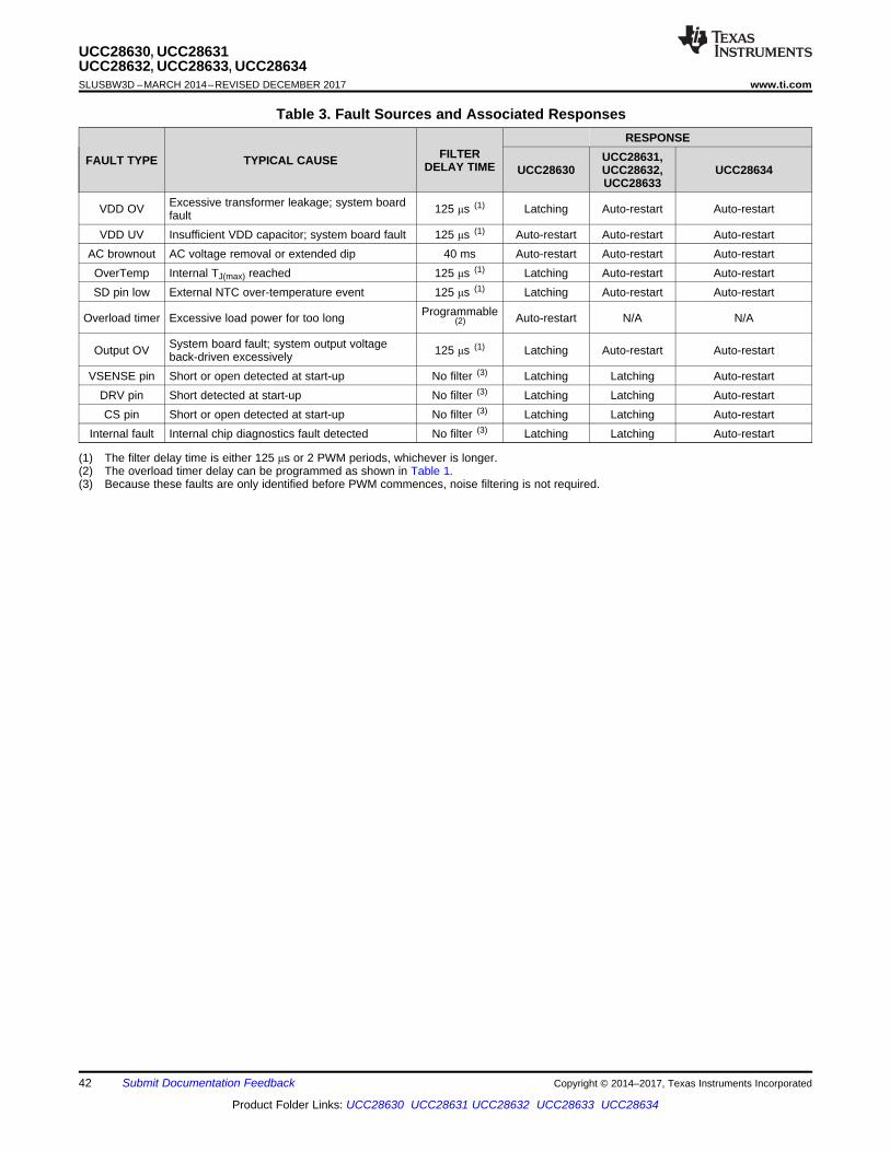
42
UCC28630, UCC28631UCC28632, UCC28633, UCC28634SLUSBW3D –MARCH 2014–REVISED DECEMBER 2017 www.ti.com
Product Folder Links: UCC28630 UCC28631 UCC28632 UCC28633 UCC28634
Submit Documentation Feedback Copyright © 2014–2017, Texas Instruments Incorporated
(1) The filter delay time is either 125 μs or 2 PWM periods, whichever is longer.(2) The overload timer delay can be programmed as shown in Table 1.(3) Because these faults are only identified before PWM commences, noise filtering is not required.
Table 3. Fault Sources and Associated Responses
FAULT TYPE TYPICAL CAUSE FILTERDELAY TIME
RESPONSE
UCC28630UCC28631,UCC28632,UCC28633
UCC28634
VDD OV Excessive transformer leakage; system boardfault 125 μs (1) Latching Auto-restart Auto-restart
VDD UV Insufficient VDD capacitor; system board fault 125 μs (1) Auto-restart Auto-restart Auto-restartAC brownout AC voltage removal or extended dip 40 ms Auto-restart Auto-restart Auto-restartOverTemp Internal TJ(max) reached 125 μs (1) Latching Auto-restart Auto-restartSD pin low External NTC over-temperature event 125 μs (1) Latching Auto-restart Auto-restart
Overload timer Excessive load power for too long Programmable(2) Auto-restart N/A N/A
Output OV System board fault; system output voltageback-driven excessively 125 μs (1) Latching Auto-restart Auto-restart
VSENSE pin Short or open detected at start-up No filter (3) Latching Latching Auto-restartDRV pin Short detected at start-up No filter (3) Latching Latching Auto-restartCS pin Short or open detected at start-up No filter (3) Latching Latching Auto-restart
Internal fault Internal chip diagnostics fault detected No filter (3) Latching Latching Auto-restart

43
UCC28630, UCC28631UCC28632, UCC28633, UCC28634
www.ti.com SLUSBW3D –MARCH 2014–REVISED DECEMBER 2017
Product Folder Links: UCC28630 UCC28631 UCC28632 UCC28633 UCC28634
Submit Documentation FeedbackCopyright © 2014–2017, Texas Instruments Incorporated
8.3.16 Pin-Fault Detection and ProtectionThe controller includes protection against most practical pin faults. These faults include open pins, pins shortedto adjacent pins, pins shorted to GND and pins shorted to VDD. The device performs pin fault checking at start-up, before the PWM is enabled. Table 4 summarizes the response to pin faults. Most faults cause either alatched shut-down, or failure to start-up. For UCC28634, all pin-faults are non-latching.
A short-circuit from the HV pin (pin 8) to the VDD pin (pin 6) is unlikely to occur, because pin 7 is not included inthe package. The HV pin and tracking requires additional PCB spacing in any event to meet creepagerequirements. However, if such a fault does occur, the device continues to charge the VDD capacitor through theHV pin external series resistor, and the power supply starts up and appears to operate normally. But because theHV and VDD pins are shorted, the internal HV current source cannot switch-out the external HV resistor, so italways dissipates power. This condition results in a large increase in no-load standby power. A 200-kΩ externalHV resistor, dissipates 66 mW at 115 VAC, and 265 mW at 230 VAC. At load levels where the X-capacitordischarge function is operational, the short to VDD appears to be an AC-disconnect event, and causes thedevice to cycle on and off.
Table 4. Pin Faults and Associated ResponsesPINS OPEN ADJACENT SHORT GND SHORT VDD SHORT
NAME NO.VSENSE 1 Latched fault Latched fault Latched fault No start-upSD 2 Normal operation Latched fault Latched fault Latched faultCS 3 Latched fault Latched fault Latched fault No start-upGND 4 Device fails, power supply
damagedLatched fault N/A No start-up
DRV 5 Hiccup fault No start-up Latched fault No start-upVDD 6 No start-up No start-up No start-up N/Ano pin 7 N/A N/A N/A N/AHV 8 No start-up N/A No start-up Fault not detected/Hiccup
fault
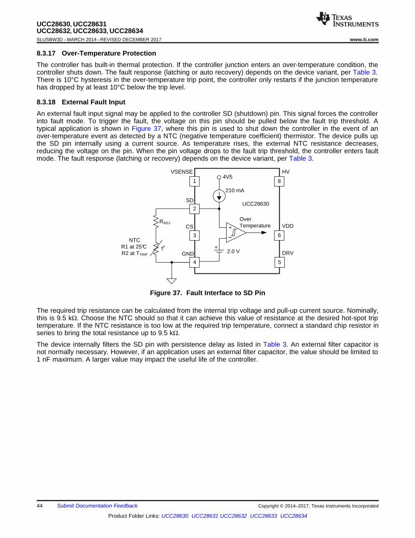
+
+
Over Temperature
4V5
210 mA
2.0 V
SD
GND
VSENSE
CS
HV
VDD
DRV
UCC28630
1
2
3
4
8
6
5
RADJ
toNTC
R1 at 25°CR2 at TTRIP
44
UCC28630, UCC28631UCC28632, UCC28633, UCC28634SLUSBW3D –MARCH 2014–REVISED DECEMBER 2017 www.ti.com
Product Folder Links: UCC28630 UCC28631 UCC28632 UCC28633 UCC28634
Submit Documentation Feedback Copyright © 2014–2017, Texas Instruments Incorporated
8.3.17 Over-Temperature ProtectionThe controller has built-in thermal protection. If the controller junction enters an over-temperature condition, thecontroller shuts down. The fault response (latching or auto recovery) depends on the device variant, per Table 3.There is 10°C hysteresis in the over-temperature trip point, the controller only restarts if the junction temperaturehas dropped by at least 10°C below the trip level.
8.3.18 External Fault InputAn external fault input signal may be applied to the controller SD (shutdown) pin. This signal forces the controllerinto fault mode. To trigger the fault, the voltage on this pin should be pulled below the fault trip threshold. Atypical application is shown in Figure 37, where this pin is used to shut down the controller in the event of anover-temperature event as detected by a NTC (negative temperature coefficient) thermistor. The device pulls upthe SD pin internally using a current source. As temperature rises, the external NTC resistance decreases,reducing the voltage on the pin. When the pin voltage drops to the fault trip threshold, the controller enters faultmode. The fault response (latching or recovery) depends on the device variant, per Table 3.
Figure 37. Fault Interface to SD Pin
The required trip resistance can be calculated from the internal trip voltage and pull-up current source. Nominally,this is 9.5 kΩ. Choose the NTC should so that it can achieve this value of resistance at the desired hot-spot triptemperature. If the NTC resistance is too low at the required trip temperature, connect a standard chip resistor inseries to bring the total resistance up to 9.5 kΩ.
The device internally filters the SD pin with persistence delay as listed in Table 3. An external filter capacitor isnot normally necessary. However, if an application uses an external filter capacitor, the value should be limited to1 nF maximum. A larger value may impact the useful life of the controller.
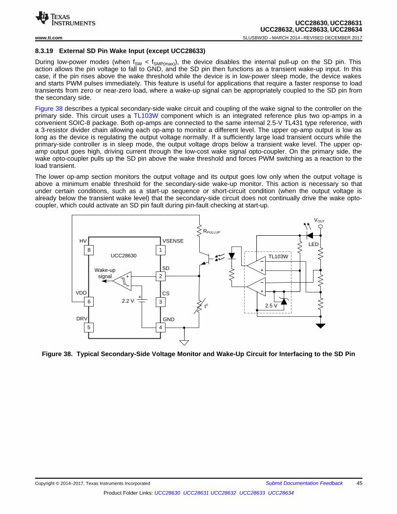
VOUT
LED
+
+
TL103W
2.5 V
SD
GND
VSENSE
CS
HV
VDD
DRV
UCC286301
2
3
4
8
6
5
Wake-up signal +
+2.2 V
to
RPULLUP
45
UCC28630, UCC28631UCC28632, UCC28633, UCC28634
www.ti.com SLUSBW3D –MARCH 2014–REVISED DECEMBER 2017
Product Folder Links: UCC28630 UCC28631 UCC28632 UCC28633 UCC28634
Submit Documentation FeedbackCopyright © 2014–2017, Texas Instruments Incorporated
8.3.19 External SD Pin Wake Input (except UCC28633)During low-power modes (when fSW < fSMP(max)), the device disables the internal pull-up on the SD pin. Thisaction allows the pin voltage to fall to GND, and the SD pin then functions as a transient wake-up input. In thiscase, if the pin rises above the wake threshold while the device is in low-power sleep mode, the device wakesand starts PWM pulses immediately. This feature is useful for applications that require a faster response to loadtransients from zero or near-zero load, where a wake-up signal can be appropriately coupled to the SD pin fromthe secondary side.
Figure 38 describes a typical secondary-side wake circuit and coupling of the wake signal to the controller on theprimary side. This circuit uses a TL103W component which is an integrated reference plus two op-amps in aconvenient SOIC-8 package. Both op-amps are connected to the same internal 2.5-V TL431 type reference, witha 3-resistor divider chain allowing each op-amp to monitor a different level. The upper op-amp output is low aslong as the device is regulating the output voltage normally. If a sufficiently large load transient occurs while theprimary-side controller is in sleep mode, the output voltage drops below a transient wake level. The upper op-amp output goes high, driving current through the low-cost wake signal opto-coupler. On the primary side, thewake opto-coupler pulls up the SD pin above the wake threshold and forces PWM switching as a reaction to theload transient.
The lower op-amp section monitors the output voltage and its output goes low only when the output voltage isabove a minimum enable threshold for the secondary-side wake-up monitor. This action is necessary so thatunder certain conditions, such as a start-up sequence or short-circuit condition (when the output voltage isalready below the transient wake level) that the secondary-side circuit does not continually drive the wake opto-coupler, which could activate an SD pin fault during pin-fault checking at start-up.
Figure 38. Typical Secondary-Side Voltage Monitor and Wake-Up Circuit for Interfacing to the SD Pin
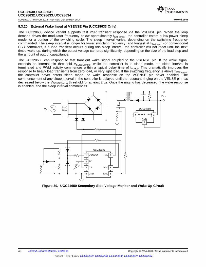
SD
GND
VSENSE
CS
HV
VDD
DRV
UCC28633
1
2
3
4
8
6
5
EMCFilter
to
VAC
VOUT
UCC24650
5 1
2
VDD
GND
WAKE
46
UCC28630, UCC28631UCC28632, UCC28633, UCC28634SLUSBW3D –MARCH 2014–REVISED DECEMBER 2017 www.ti.com
Product Folder Links: UCC28630 UCC28631 UCC28632 UCC28633 UCC28634
Submit Documentation Feedback Copyright © 2014–2017, Texas Instruments Incorporated
8.3.20 External Wake Input at VSENSE Pin (UCC28633 Only)The UCC28633 device variant supports fast PSR transient response via the VSENSE pin. When the loopdemand drives the modulator frequency below approximately fSMP(max), the controller enters a low-power sleepmode for a portion of the switching cycle. The sleep interval varies, depending on the switching frequencycommanded. The sleep interval is longer for lower switching frequency, and longest at fSW(min). For conventionalPSR controllers, if a load transient occurs during this sleep interval, the controller will not react until the nexttimed wake-up, during which the output voltage can drop significantly, depending on the size of the load step andthe amount of output capacitance.
The UCC28633 can respond to fast transient wake signal coupled to the VSENSE pin. If the wake signalexceeds an internal pin threshold VSENSE(wake) while the controller is in sleep mode, the sleep interval isterminated and PWM activity commences within a typical delay time of tWAKE. This dramatically improves theresponse to heavy load transients from zero load, or very light load. If the switching frequency is above fSMP(max),the controller never enters sleep mode, so wake response on the VSENSE pin never enabled. Thecommencement of any sleep interval in the controller is delayed until the resonant ringing on the VENSE pin hasdecreased below the VSENSE(wake) threshold for at least 2 µs. Once the ringing has decreased, the wake responseis enabled, and the sleep interval commences.
Figure 39. UCC24650 Secondary-Side Voltage Monitor and Wake-Up Circuit
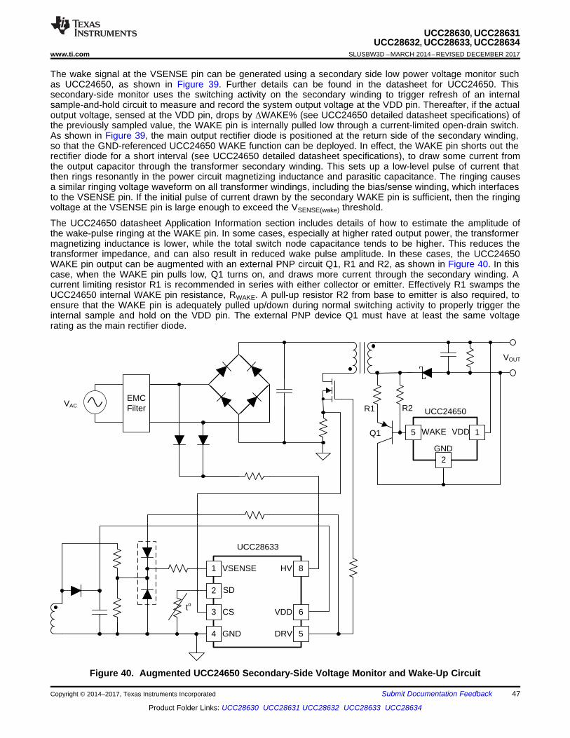
SD
GND
VSENSE
CS
HV
VDD
DRV
UCC28633
1
2
3
4
8
6
5
EMCFilter
to
VAC
VOUT
UCC24650
Q1
R1 R2
5 1
2
VDD
GND
WAKE
47
UCC28630, UCC28631UCC28632, UCC28633, UCC28634
www.ti.com SLUSBW3D –MARCH 2014–REVISED DECEMBER 2017
Product Folder Links: UCC28630 UCC28631 UCC28632 UCC28633 UCC28634
Submit Documentation FeedbackCopyright © 2014–2017, Texas Instruments Incorporated
The wake signal at the VSENSE pin can be generated using a secondary side low power voltage monitor suchas UCC24650, as shown in Figure 39. Further details can be found in the datasheet for UCC24650. Thissecondary-side monitor uses the switching activity on the secondary winding to trigger refresh of an internalsample-and-hold circuit to measure and record the system output voltage at the VDD pin. Thereafter, if the actualoutput voltage, sensed at the VDD pin, drops by ΔWAKE% (see UCC24650 detailed datasheet specifications) ofthe previously sampled value, the WAKE pin is internally pulled low through a current-limited open-drain switch.As shown in Figure 39, the main output rectifier diode is positioned at the return side of the secondary winding,so that the GND-referenced UCC24650 WAKE function can be deployed. In effect, the WAKE pin shorts out therectifier diode for a short interval (see UCC24650 detailed datasheet specifications), to draw some current fromthe output capacitor through the transformer secondary winding. This sets up a low-level pulse of current thatthen rings resonantly in the power circuit magnetizing inductance and parasitic capacitance. The ringing causesa similar ringing voltage waveform on all transformer windings, including the bias/sense winding, which interfacesto the VSENSE pin. If the initial pulse of current drawn by the secondary WAKE pin is sufficient, then the ringingvoltage at the VSENSE pin is large enough to exceed the VSENSE(wake) threshold.
The UCC24650 datasheet Application Information section includes details of how to estimate the amplitude ofthe wake-pulse ringing at the WAKE pin. In some cases, especially at higher rated output power, the transformermagnetizing inductance is lower, while the total switch node capacitance tends to be higher. This reduces thetransformer impedance, and can also result in reduced wake pulse amplitude. In these cases, the UCC24650WAKE pin output can be augmented with an external PNP circuit Q1, R1 and R2, as shown in Figure 40. In thiscase, when the WAKE pin pulls low, Q1 turns on, and draws more current through the secondary winding. Acurrent limiting resistor R1 is recommended in series with either collector or emitter. Effectively R1 swamps theUCC24650 internal WAKE pin resistance, RWAKE. A pull-up resistor R2 from base to emitter is also required, toensure that the WAKE pin is adequately pulled up/down during normal switching activity to properly trigger theinternal sample and hold on the VDD pin. The external PNP device Q1 must have at least the same voltagerating as the main rectifier diode.
Figure 40. Augmented UCC24650 Secondary-Side Voltage Monitor and Wake-Up Circuit
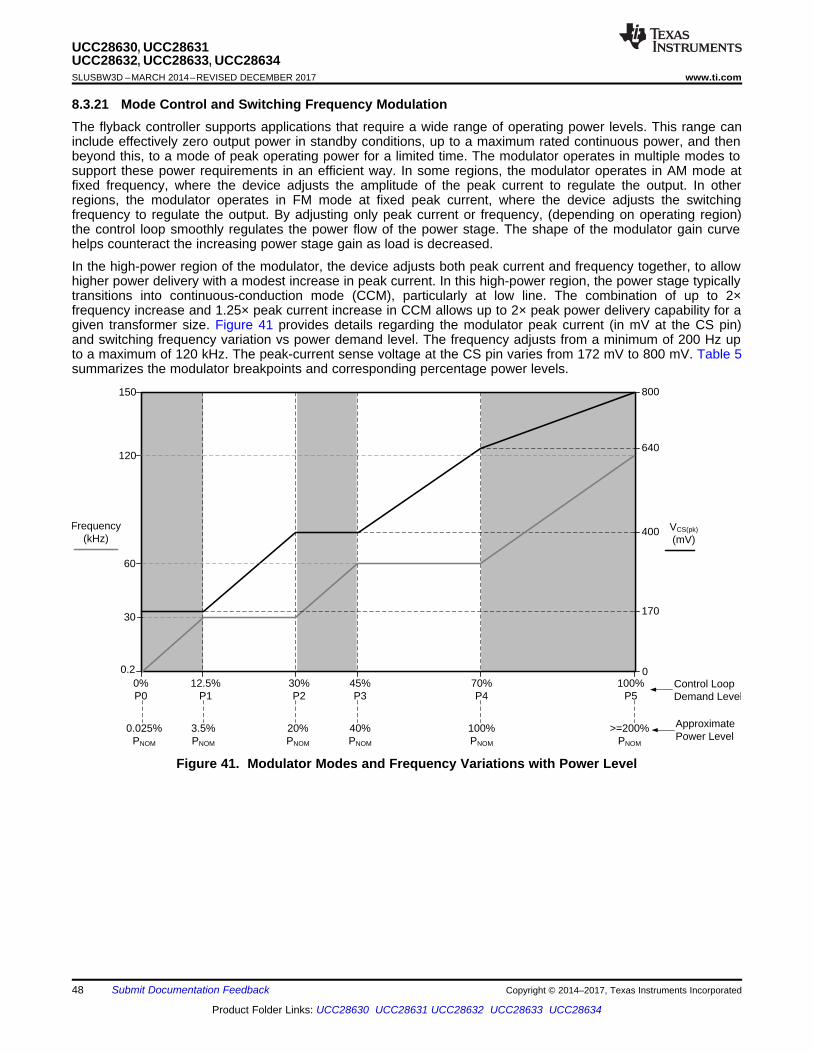
0%P0
12.5%P1
30%P2
45%P3
70%P4
100%P5
0.2
30
60
150
0
170
400
640
800
Frequency(kHz)
VCS(pk)
(mV)
Control Loop Demand Level
0.025%PNOM
3.5%PNOM
20%PNOM
40%PNOM
100%PNOM
>=200%PNOM
Approximate Power Level
120
48
UCC28630, UCC28631UCC28632, UCC28633, UCC28634SLUSBW3D –MARCH 2014–REVISED DECEMBER 2017 www.ti.com
Product Folder Links: UCC28630 UCC28631 UCC28632 UCC28633 UCC28634
Submit Documentation Feedback Copyright © 2014–2017, Texas Instruments Incorporated
8.3.21 Mode Control and Switching Frequency ModulationThe flyback controller supports applications that require a wide range of operating power levels. This range caninclude effectively zero output power in standby conditions, up to a maximum rated continuous power, and thenbeyond this, to a mode of peak operating power for a limited time. The modulator operates in multiple modes tosupport these power requirements in an efficient way. In some regions, the modulator operates in AM mode atfixed frequency, where the device adjusts the amplitude of the peak current to regulate the output. In otherregions, the modulator operates in FM mode at fixed peak current, where the device adjusts the switchingfrequency to regulate the output. By adjusting only peak current or frequency, (depending on operating region)the control loop smoothly regulates the power flow of the power stage. The shape of the modulator gain curvehelps counteract the increasing power stage gain as load is decreased.
In the high-power region of the modulator, the device adjusts both peak current and frequency together, to allowhigher power delivery with a modest increase in peak current. In this high-power region, the power stage typicallytransitions into continuous-conduction mode (CCM), particularly at low line. The combination of up to 2×frequency increase and 1.25× peak current increase in CCM allows up to 2× peak power delivery capability for agiven transformer size. Figure 41 provides details regarding the modulator peak current (in mV at the CS pin)and switching frequency variation vs power demand level. The frequency adjusts from a minimum of 200 Hz upto a maximum of 120 kHz. The peak-current sense voltage at the CS pin varies from 172 mV to 800 mV. Table 5summarizes the modulator breakpoints and corresponding percentage power levels.
Figure 41. Modulator Modes and Frequency Variations with Power Level

49
UCC28630, UCC28631UCC28632, UCC28633, UCC28634
www.ti.com SLUSBW3D –MARCH 2014–REVISED DECEMBER 2017
Product Folder Links: UCC28630 UCC28631 UCC28632 UCC28633 UCC28634
Submit Documentation FeedbackCopyright © 2014–2017, Texas Instruments Incorporated
For no load and very light loads (P0 to P1 region) the modulator operates in a pulse frequency modulation (PFM)mode. In PFM mode, the device maintains a constant peak current in the transformer magnetizing inductance, sothat the energy transferred in each switching cycle is fixed. The magnetic sensing, fixed-point sampling schemerequires that the device always imposes a minimum peak current. This minimum peak-current demand naturallyresults in a minimum transformer magnetizing volt-second product that the device maintains across the input linevoltage range. Ensuring a minimum on-time magnetizing volt-seconds also ensures a balancing volt-secondflyback interval, during which the device guarantees the availability of the output voltage sample. MagneticSensing: Power Stage Design Constraints outlines the transformer design constraints necessary to comply withthe minimum on-time and minimum required volt-seconds.
In the P0 to P1 region, the energy transfer per switching cycle is maximized, which in turn minimizes the switchingfrequency and associated switching and drive losses, to improve efficiency. However, due to concerns aboutaudible noise in this region, the peak current VCS(min) in this region is limited to 22% of the peak VCS(max) at themaximum demand level. This peak-current derating maintains the transformer peak flux density to 22% of thepeak, to minimize transformer-induced audible noise. Assuming a maximum peak flux density of typically 300 mTat highest peak current, this derating sets the peak flux level at approximately 65 mT in the light-load region.Empirically, this flux level greatly reduces magnetic audible noise for a variety of power levels and transformerdesigns. In this region, the use of sleep modes (where most of the device internal blocks are powered down inbetween switching cycles) minimizes the controller power consumption. Minimizing controller power consumptionhelps reduce total standby power consumption, and also greatly eases the bias design constraints.
For higher loads above P1 (P1 to P2 region), the device fixes the modulator frequency at a low value above theaudible range, while the peak switch current ramps up from the minimum level, to deliver the increased outputpower. Maintaining a fixed low-switching frequency while ramping peak current, minimizes switching losses toprovide good light-load efficiency.
For higher loads above P2 (P2 to P3 region), the device maintains a constant peak-switch current, while themodulator frequency ramps to its nominal operating value. The normal heavy load (between 40% and 100% ofrated) operating power range lies between P3 and P4. In this region the device maintains a constant switchingfrequency at the nominal value fSW(nom), and the peak switch current ramps to achieve increased output power.Fixed-frequency operation at nominal operating power results in consistent EMI and transient load stepperformance.
Table 5. Frequency and Peak-Current Modulator Operating Ranges and BreakpointsMODULATORBREAKPOINT
DEMAND LEVEL(%)
APPROXIMATEPOWER
LEVEL % ofPNOM
VCS PEAK FREQUENCY fSW
(mV) (kHz)
PO0 0 0.025 172 VCS(min) 0.200 fSW(min)
PO1 12.5 3.5 172 VCS(min) 30 fSW(LL)
PO2 30 20 400 VCS(nom) 30 fSW(LL)
PO3 45 40 400 VCS(nom) 60 fSW(nom)
PO4 70 100 640 VCS(bcm) 60 fSW(nom)
PO5 100 > 200 800 VCS(max) 120 fSW(max)
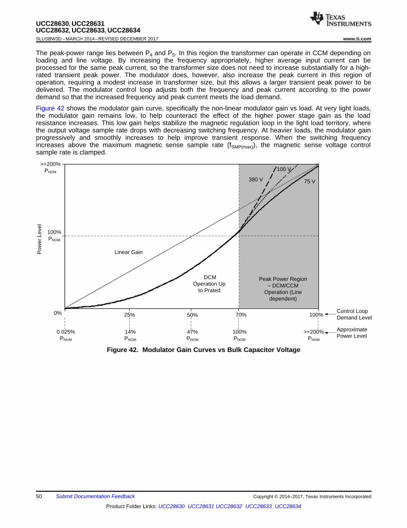
0% 25% 50% 70% 100%
100%PNOM
>=200%PNOM
Pow
er L
evel
Peak Power Region ± DCM/CCM
Operation (Line dependent)
380 V 75 V
100 V
Linear Gain
0.025%PNOM
14%PNOM
47%PNOM
100%PNOM
>=200%PNOM
Approximate Power Level
Control Loop Demand Level
DCM Operation Up
to Prated
50
UCC28630, UCC28631UCC28632, UCC28633, UCC28634SLUSBW3D –MARCH 2014–REVISED DECEMBER 2017 www.ti.com
Product Folder Links: UCC28630 UCC28631 UCC28632 UCC28633 UCC28634
Submit Documentation Feedback Copyright © 2014–2017, Texas Instruments Incorporated
The peak-power range lies between P4 and P5. In this region the transformer can operate in CCM depending onloading and line voltage. By increasing the frequency appropriately, higher average input current can beprocessed for the same peak current, so the transformer size does not need to increase substantially for a high-rated transient peak power. The modulator does, however, also increase the peak current in this region ofoperation, requiring a modest increase in transformer size, but this allows a larger transient peak power to bedelivered. The modulator control loop adjusts both the frequency and peak current according to the powerdemand so that the increased frequency and peak current meets the load demand.
Figure 42 shows the modulator gain curve, specifically the non-linear modulator gain vs load. At very light loads,the modulator gain remains low, to help counteract the effect of the higher power stage gain as the loadresistance increases. This low gain helps stabilize the magnetic regulation loop in the light load territory, wherethe output voltage sample rate drops with decreasing switching frequency. At heavier loads, the modulator gainprogressively and smoothly increases to help improve transient response. When the switching frequencyincreases above the maximum magnetic sense sample rate (fSMP(max)), the magnetic sense voltage controlsample rate is clamped.
Figure 42. Modulator Gain Curves vs Bulk Capacitor Voltage
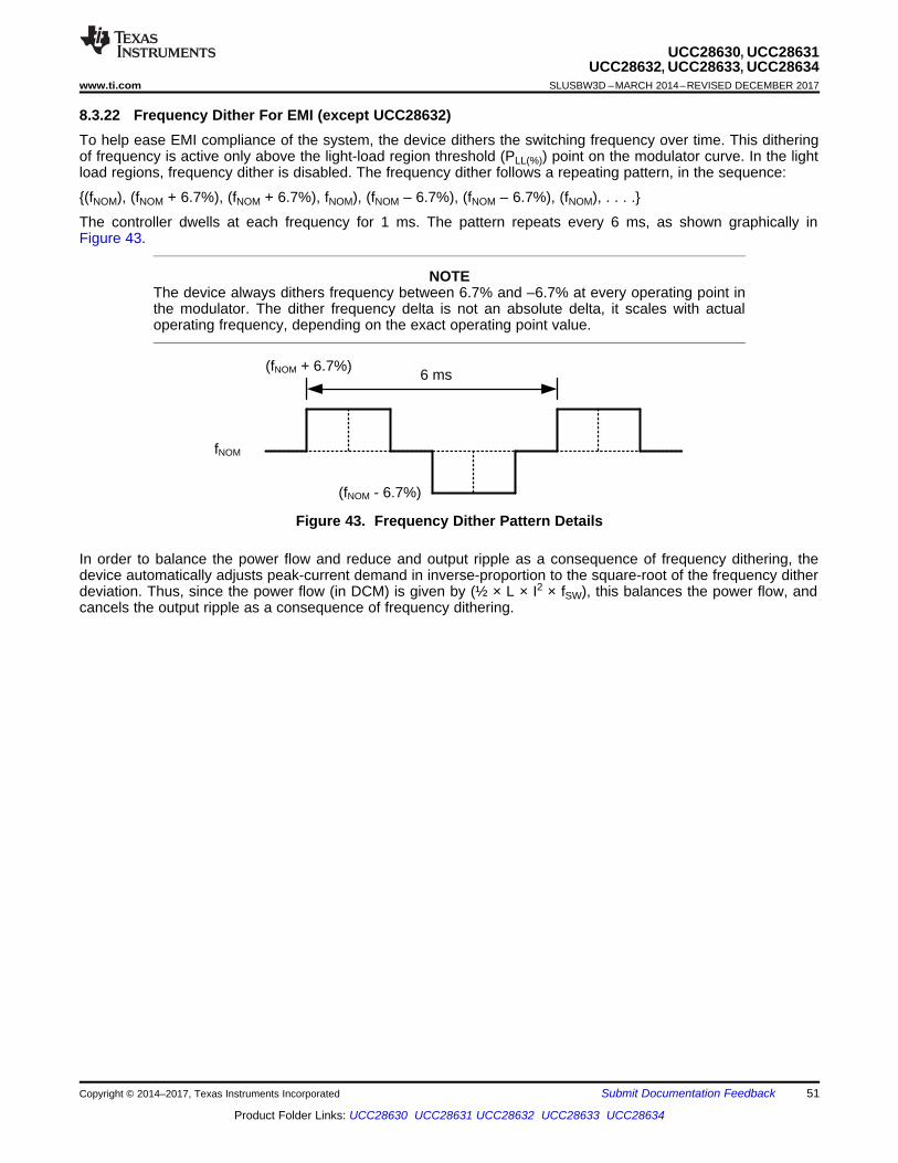
(fNOM - 6.7%)
(fNOM + 6.7%)
fNOM
6 ms
51
UCC28630, UCC28631UCC28632, UCC28633, UCC28634
www.ti.com SLUSBW3D –MARCH 2014–REVISED DECEMBER 2017
Product Folder Links: UCC28630 UCC28631 UCC28632 UCC28633 UCC28634
Submit Documentation FeedbackCopyright © 2014–2017, Texas Instruments Incorporated
8.3.22 Frequency Dither For EMI (except UCC28632)To help ease EMI compliance of the system, the device dithers the switching frequency over time. This ditheringof frequency is active only above the light-load region threshold (PLL(%)) point on the modulator curve. In the lightload regions, frequency dither is disabled. The frequency dither follows a repeating pattern, in the sequence:
(fNOM), (fNOM + 6.7%), (fNOM + 6.7%), fNOM), (fNOM – 6.7%), (fNOM – 6.7%), (fNOM), . . . .
The controller dwells at each frequency for 1 ms. The pattern repeats every 6 ms, as shown graphically inFigure 43.
NOTEThe device always dithers frequency between 6.7% and –6.7% at every operating point inthe modulator. The dither frequency delta is not an absolute delta, it scales with actualoperating frequency, depending on the exact operating point value.
Figure 43. Frequency Dither Pattern Details
In order to balance the power flow and reduce and output ripple as a consequence of frequency dithering, thedevice automatically adjusts peak-current demand in inverse-proportion to the square-root of the frequency ditherdeviation. Thus, since the power flow (in DCM) is given by (½ × L × I2 × fSW), this balances the power flow, andcancels the output ripple as a consequence of frequency dithering.
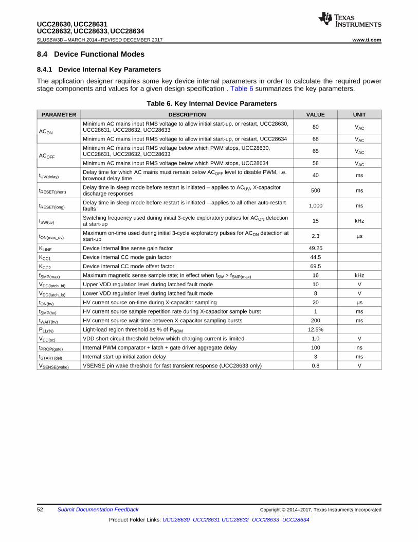
52
UCC28630, UCC28631UCC28632, UCC28633, UCC28634SLUSBW3D –MARCH 2014–REVISED DECEMBER 2017 www.ti.com
Product Folder Links: UCC28630 UCC28631 UCC28632 UCC28633 UCC28634
Submit Documentation Feedback Copyright © 2014–2017, Texas Instruments Incorporated
8.4 Device Functional Modes
8.4.1 Device Internal Key ParametersThe application designer requires some key device internal parameters in order to calculate the required powerstage components and values for a given design specification . Table 6 summarizes the key parameters.
Table 6. Key Internal Device ParametersPARAMETER DESCRIPTION VALUE UNIT
ACON
Minimum AC mains input RMS voltage to allow initial start-up, or restart, UCC28630,UCC28631, UCC28632, UCC28633 80 VAC
Minimum AC mains input RMS voltage to allow initial start-up, or restart, UCC28634 68 VAC
ACOFF
Minimum AC mains input RMS voltage below which PWM stops, UCC28630,UCC28631, UCC28632, UCC28633 65 VAC
Minimum AC mains input RMS voltage below which PWM stops, UCC28634 58 VAC
tUV(delay)Delay time for which AC mains must remain below ACOFF level to disable PWM, i.e.brownout delay time 40 ms
tRESET(short)Delay time in sleep mode before restart is initiated – applies to ACUV, X-capacitordischarge responses 500 ms
tRESET(long)Delay time in sleep mode before restart is initiated – applies to all other auto-restartfaults 1,000 ms
fSW(uv)Switching frequency used during initial 3-cycle exploratory pulses for ACON detectionat start-up 15 kHz
tON(max_uv)Maximum on-time used during initial 3-cycle exploratory pulses for ACON detection atstart-up 2.3 µs
KLINE Device internal line sense gain factor 49.25KCC1 Device internal CC mode gain factor 44.5KCC2 Device internal CC mode offset factor 69.5fSMP(max) Maximum magnetic sense sample rate; in effect when fSW > fSMP(max) 16 kHzVDD(latch_hi) Upper VDD regulation level during latched fault mode 10 VVDD(latch_lo) Lower VDD regulation level during latched fault mode 8 VtON(hv) HV current source on-time during X-capacitor sampling 20 µstSMP(hv) HV current source sample repetition rate during X-capacitor sample burst 1 mstWAIT(hv) HV current source wait-time between X-capacitor sampling bursts 200 msPLL(%) Light-load region threshold as % of PNOM 12.5%VDD(sc) VDD short-circuit threshold below which charging current is limited 1.0 VtPROP(gate) Internal PWM comparator + latch + gate driver aggregate delay 100 nstSTART(del) Internal start-up initialization delay 3 msVSENSE(wake) VSENSE pin wake threshold for fast transient response (UCC28633 only) 0.8 V
53
UCC28630, UCC28631UCC28632, UCC28633, UCC28634
www.ti.com SLUSBW3D –MARCH 2014–REVISED DECEMBER 2017
Product Folder Links: UCC28630 UCC28631 UCC28632 UCC28633 UCC28634
Submit Documentation FeedbackCopyright © 2014–2017, Texas Instruments Incorporated
9 Applications and Implementation
NOTEInformation in the following applications sections is not part of the TI componentspecification, and TI does not warrant its accuracy or completeness. TI’s customers areresponsible for determining suitability of components for their purposes. Customers shouldvalidate and test their design implementation to confirm system functionality.
9.1 Application InformationThe UCC2863x device is a highly integrated primary-side-regulated (PSR) flyback controller, supportingmagnetically-sensed output voltage regulation via the transformer bias winding. This sensing eliminates the needfor a secondary-side reference, error amplifier and opto-isolator for output voltage regulation. The device deliversaccurate output voltage static load and line regulation, and accurate control of the output constant-current limit.
The fixed-point magnetic sampling scheme allows operation in both continuous conduction mode (CCM) anddiscontinuous conduction mode (DCM). The combination of the sampling scheme and high current gate driversource and sink capability, makes this device ideal for high power flyback converters up to 100 W and beyond.
The modulator adjusts both frequency and peak current in different load regions to maximize efficiencythroughout the operating range. The control approach improves performance (efficiency, size and cost) and canreduce transformer size and cost by allowing operation in CCM with FM during peak overload conditions. Themodulator supports peak-to-average transient overload power up to 200% of the nominal average rating.
9.2 Typical Application
9.2.1 Notebook Adapter, 19.5 V, 65 WThis design example describes the PWR572 EVM design and outlines the design steps required to design aconstant-voltage, constant-current flyback converter for a 19.5-V/65-W notebook adapter. For all equations anddesign steps, refer to Table 6 for definitions and values of key internal device parameters that are relevant forcalculations of external component values.
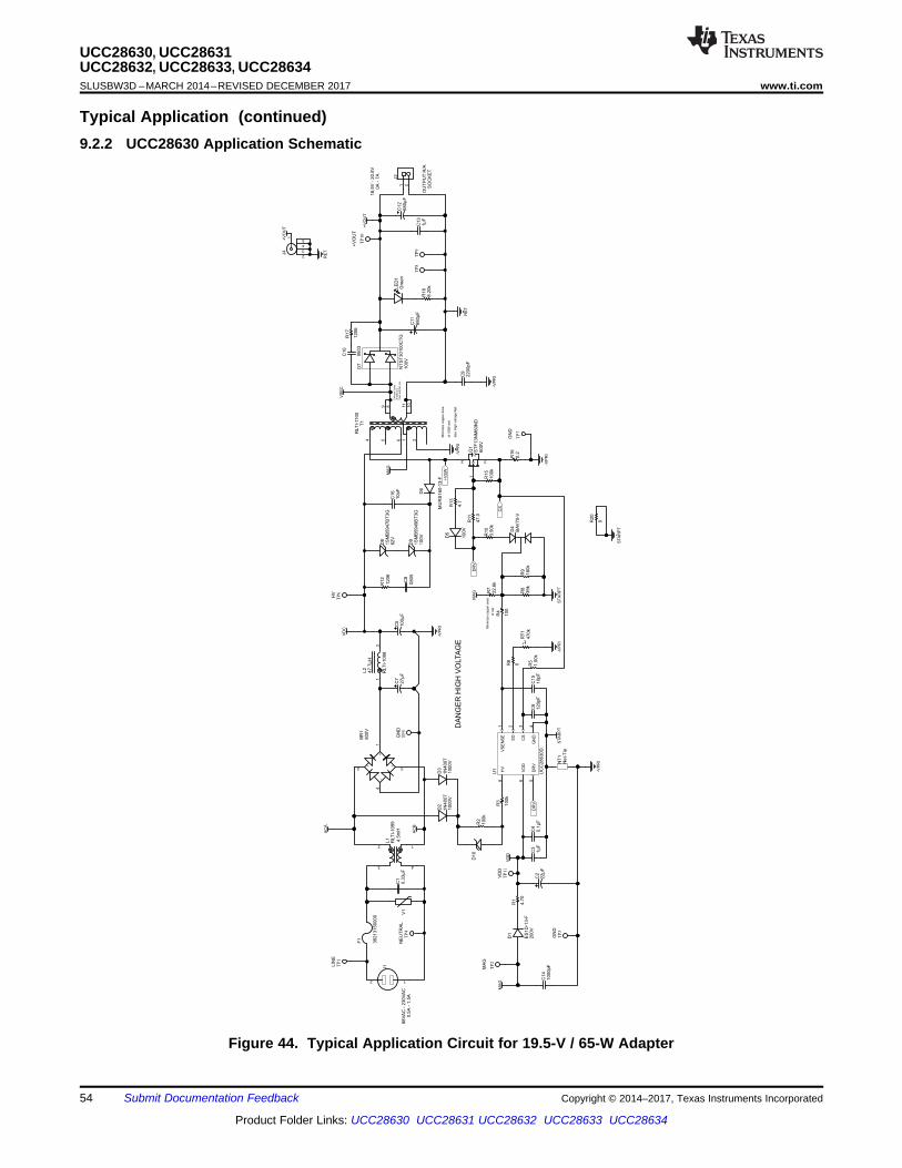
Min
imiz
ecopper
are
a
als
oH
igh
voltage
Net
of
VS
Wnet
Min
imiz
ecopper
are
a
of
net
Connect
2pin
sof
bobbin
toV
sec
and
Re
tnets
47.0
R11
0.2
R16
0.1
µF
C4
TP
9
TP
6
TP
7
2200pF
C9
TP
8
TP
10
1µ
FC
3
4.7
R13
100V
D5
0603
C10
1206
R17
39k
R8
100k
R15
100
R4
TP
3
TP
5
4.7
0
R1
120pF
C6
3.9
0k
R10
TP
2
1.0
0k
R5
BA
V70
-VD
40R
6
-VP
RI
VD
D
+V
OU
T
VD
C
AC
A
AC
B
VS
EC
+V
SW
-VP
RI
-VP
RI
STA
RP
T
DR
V
CS
-VP
RI
MA
G
MA
G
DR
V
RE
T
STA
RP
T-V
PR
I
TP
1
TP
4
F1
39213150000
V1
0.3
3µ
FC
1
1000V
D3
1N
4007
1000V
D2
1N
4007
100k
R3
MU
RS
160-1
3-F
D6
1
32
600V
Q1
ST
F13N
M60N
D
180k
R9
22.6
kR
7
t° 470k
RT
1
NT
1N
et-
Tie
22µ
FC
2
ES
1D
-13-F
200V
D1
100V
D7
NT
ST
30100C
TG
VS
EN
SE
1
SD
2
CS
3
GN
D4
DR
V5
VD
D6
HV
8
U1
UC
C28630D
MA
G
-VP
RI
2 1
J1
~3
+1
~2
-4
800V
BR
1
47.7
µH
13
L2
RLT
I-1098
LIN
E
NE
UT
RA
LG
ND
HV
GN
D
MA
G
GN
D
+V
OU
T
0R20
27µ
FC
7
1000pF
C14
D10
100k
R2
10pF
C15
8.2
0k
R18
OU
TP
UT
R/A
SO
CK
ET
12
3 4
4.5
mH
L1
RLT
I-1099
STA
RP
T
1206
R12
0805
C8
82V
D8
1S
MB
5947B
T3
G
100V
D9
1S
MB
5949B
T3
G
10pF
C16
1
2
3
4
5
J4
+V
OU
T
RE
T
TP
11
VD
D
100µ
FC
51 2
J2
Gre
en
LE
D1
88
VA
C-
230
VA
C0.5
A-
1.5
A
18.5
V-
20.5
V0A
-7A
DA
NG
ER
HIG
HV
OLTA
GE
680µ
FC
12
1µ
FC
13
680µ
FC
11
1 2
11
8
54 6
9 10
T1
RLT
I-1100
54
UCC28630, UCC28631UCC28632, UCC28633, UCC28634SLUSBW3D –MARCH 2014–REVISED DECEMBER 2017 www.ti.com
Product Folder Links: UCC28630 UCC28631 UCC28632 UCC28633 UCC28634
Submit Documentation Feedback Copyright © 2014–2017, Texas Instruments Incorporated
Typical Application (continued)9.2.2 UCC28630 Application Schematic
Figure 44. Typical Application Circuit for 19.5-V / 65-W Adapter

CBULK=
POUT
D × L0.5+
1
N × sin-1 F VBULK:min ;
¾2 × VAC:min ;GMk2 × V
AC:min ;2 F VBULK:min ;2 o × fLINE:min ;
55
UCC28630, UCC28631UCC28632, UCC28633, UCC28634
www.ti.com SLUSBW3D –MARCH 2014–REVISED DECEMBER 2017
Product Folder Links: UCC28630 UCC28631 UCC28632 UCC28633 UCC28634
Submit Documentation FeedbackCopyright © 2014–2017, Texas Instruments Incorporated
Typical Application (continued)9.2.3 Design Requirements
Table 7. Design RequirementsDESIGN PARAMETER TARGET VALUE
Output voltage 19.5 VRated (continuous) output power 65 WPeak (transient) output power 130 WPeak (transient) output power duration 2 msInput AC voltage range 88 VRMS to 264 VRMS
Typical efficiency 88%Minimum bulk voltage at 88 VAC/47 Hz and rated (continuous) output power 82 V
9.2.4 Detailed Design Procedure
9.2.4.1 Custom Design With WEBENCH® ToolsClick here to create a custom design using the UCC2863x device with the WEBENCH® Power Designer.1. Start by entering the input voltage (VIN), output voltage (VOUT), and output current (IOUT) requirements.2. Optimize the design for key parameters such as efficiency, footprint, and cost using the optimizer dial.3. Compare the generated design with other possible solutions from Texas Instruments.
The WEBENCH Power Designer provides a customized schematic along with a list of materials with real-timepricing and component availability.
In most cases, these actions are available:• Run electrical simulations to see important waveforms and circuit performance• Run thermal simulations to understand board thermal performance• Export customized schematic and layout into popular CAD formats• Print PDF reports for the design, and share the design with colleagues
Get more information about WEBENCH tools at www.ti.com/WEBENCH.
9.2.4.2 Input Bulk Capacitance and Minimum Bulk VoltageThe required bulk capacitance value depends on the target minimum bulk capacitor ripple voltage at minimumAC input line, minimum line frequency and on the power level of interest. As a way of estimating, use 1.5-μF to2-μF per Watt of rated, continuous power to achieve approximately 70 V to 80 V minimum at 88 VRMS input. Thiscase indicates a required bulk capacitance of between approximately 100 μF and 130 μF. Alternatively, therequired capacitance may be explicitly calculated for a specific set of requirements using Equation 21.
(21)
Using the parameters in Table 7, this calculates a required CBULK of 130 μF.
To help reduce differential mode (DM) emissions for conducted EMC compliance, the bulk capacitance has beensplit into two separate capacitors C5 and C7 in Figure 44, with a small DM choke L2 inserted between thecapacitors. The total resulting capacitance of 127 μF is close to the required minimum requirement perEquation 21, and the design results in a small decrease in the actual bulk capacitor minimum ripple voltage.
Next, verify that the choice of bulk capacitance satisfies the X-capacitor discharge constraints for rate ofdischarge by the load when X-capacitor sampling is inactive, per Equation 5. The bulk capacitance should beless than the value calculated by Equation 22.
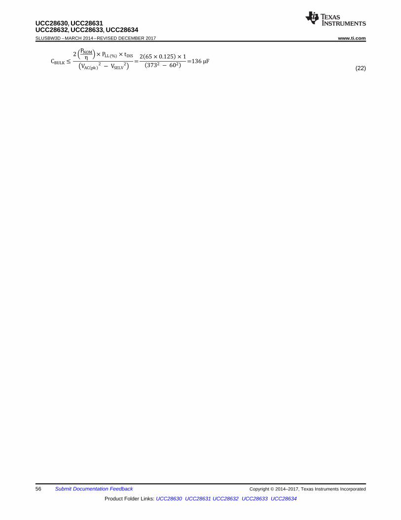
CBULK Q2@PNOM
DA× PLL(%) × tDIS
kVAC:pk;2 F VSELV
2o=
2:65 × 0.125; × 1
:3732 F 602; LsuxJF
56
UCC28630, UCC28631UCC28632, UCC28633, UCC28634SLUSBW3D –MARCH 2014–REVISED DECEMBER 2017 www.ti.com
Product Folder Links: UCC28630 UCC28631 UCC28632 UCC28633 UCC28634
Submit Documentation Feedback Copyright © 2014–2017, Texas Instruments Incorporated
(22)
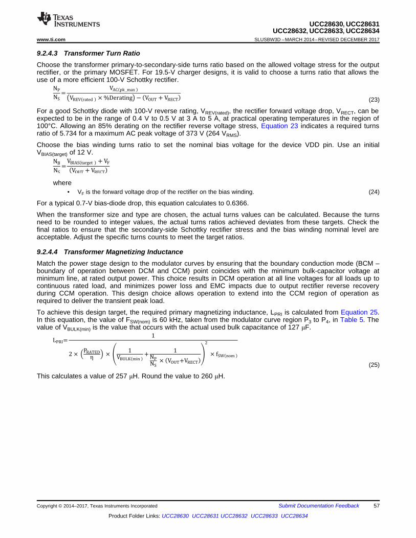
LPRI=1
2 × @PRATED
DA × L 1
VBULK:min ; +1
NP
NS
× :VOUT+VRECT;M2
× fSW:nom ;
NB
NS
=VBIAS:target ; + VF
:VOUT + VRECT;
NP
NS
=VAC:pk _max ;
kVREV:rated ; × %Deratingo F :VOUT + VRECT;
57
UCC28630, UCC28631UCC28632, UCC28633, UCC28634
www.ti.com SLUSBW3D –MARCH 2014–REVISED DECEMBER 2017
Product Folder Links: UCC28630 UCC28631 UCC28632 UCC28633 UCC28634
Submit Documentation FeedbackCopyright © 2014–2017, Texas Instruments Incorporated
9.2.4.3 Transformer Turn RatioChoose the transformer primary-to-secondary-side turns ratio based on the allowed voltage stress for the outputrectifier, or the primary MOSFET. For 19.5-V charger designs, it is valid to choose a turns ratio that allows theuse of a more efficient 100-V Schottky rectifier.
(23)
For a good Schottky diode with 100-V reverse rating, VREV(rated), the rectifier forward voltage drop, VRECT, can beexpected to be in the range of 0.4 V to 0.5 V at 3 A to 5 A, at practical operating temperatures in the region of100°C. Allowing an 85% derating on the rectifier reverse voltage stress, Equation 23 indicates a required turnsratio of 5.734 for a maximum AC peak voltage of 373 V (264 VRMS).
Choose the bias winding turns ratio to set the nominal bias voltage for the device VDD pin. Use an initialVBIAS(target) of 12 V.
where• VF is the forward voltage drop of the rectifier on the bias winding. (24)
For a typical 0.7-V bias-diode drop, this equation calculates to 0.6366.
When the transformer size and type are chosen, the actual turns values can be calculated. Because the turnsneed to be rounded to integer values, the actual turns ratios achieved deviates from these targets. Check thefinal ratios to ensure that the secondary-side Schottky rectifier stress and the bias winding nominal level areacceptable. Adjust the specific turns counts to meet the target ratios.
9.2.4.4 Transformer Magnetizing InductanceMatch the power stage design to the modulator curves by ensuring that the boundary conduction mode (BCM –boundary of operation between DCM and CCM) point coincides with the minimum bulk-capacitor voltage atminimum line, at rated output power. This choice results in DCM operation at all line voltages for all loads up tocontinuous rated load, and minimizes power loss and EMC impacts due to output rectifier reverse recoveryduring CCM operation. This design choice allows operation to extend into the CCM region of operation asrequired to deliver the transient peak load.
To achieve this design target, the required primary magnetizing inductance, LPRI is calculated from Equation 25.In this equation, the value of FSW(nom) is 60 kHz, taken from the modulator curve region P3 to P4, in Table 5. Thevalue of VBULK(min) is the value that occurs with the actual used bulk capacitance of 127 μF.
(25)
This calculates a value of 257 μH. Round the value to 260 μH.
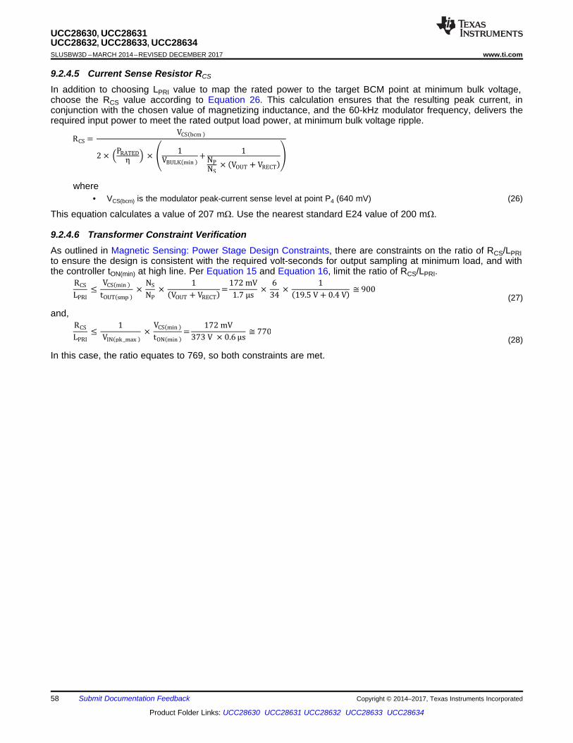
RCS
LPRI
Q1
VIN:pk _max ; ×
VCS:min ;
tON:min ;=
172 mV
373 V × 0.6 Js yyr
RCS
LPRI
QVCS:min ;
tOUT:smp ; ×
NS
NP
× 1
:VOUT + VRECT;=
172 mV
säyJs ×
6
34 ×
1
:19.5 V + 0.4 V; rr
RCS = VCS:bcm ;
2 × @PRATED
DA × L 1
VBULK:min ; +1
NP
NS
× :VOUT + VRECT;M
58
UCC28630, UCC28631UCC28632, UCC28633, UCC28634SLUSBW3D –MARCH 2014–REVISED DECEMBER 2017 www.ti.com
Product Folder Links: UCC28630 UCC28631 UCC28632 UCC28633 UCC28634
Submit Documentation Feedback Copyright © 2014–2017, Texas Instruments Incorporated
9.2.4.5 Current Sense Resistor RCS
In addition to choosing LPRI value to map the rated power to the target BCM point at minimum bulk voltage,choose the RCS value according to Equation 26. This calculation ensures that the resulting peak current, inconjunction with the chosen value of magnetizing inductance, and the 60-kHz modulator frequency, delivers therequired input power to meet the rated output load power, at minimum bulk voltage ripple.
where• VCS(bcm) is the modulator peak-current sense level at point P4 (640 mV) (26)
This equation calculates a value of 207 mΩ. Use the nearest standard E24 value of 200 mΩ.
9.2.4.6 Transformer Constraint VerificationAs outlined in Magnetic Sensing: Power Stage Design Constraints, there are constraints on the ratio of RCS/LPRIto ensure the design is consistent with the required volt-seconds for output sampling at minimum load, and withthe controller tON(min) at high line. Per Equation 15 and Equation 16, limit the ratio of RCS/LPRI.
(27)
and,
(28)
In this case, the ratio equates to 769, so both constraints are met.
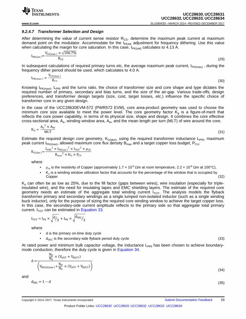
dSEC = 1Fd
d =
NP
NS
× :VOUT + VRECT;FVBULK:min ;+ NP
NS
× :VOUT + VRECT;G
ITOT = IPK × §d3W + IPK × §dSEC
3W
KG:des ;=LPRI
2 × IPK:sat ;
2 × ITOT
2 × OCU
Bmax
2 × KU × PCU
KG = Ae
2 × AW
MLT
IPK:max ; = VCS:max ;
RCS
IPK:sat ;=VCS:max ; × ¾106.7%
RCS
59
UCC28630, UCC28631UCC28632, UCC28633, UCC28634
www.ti.com SLUSBW3D –MARCH 2014–REVISED DECEMBER 2017
Product Folder Links: UCC28630 UCC28631 UCC28632 UCC28633 UCC28634
Submit Documentation FeedbackCopyright © 2014–2017, Texas Instruments Incorporated
9.2.4.7 Transformer Selection and DesignAfter determining the value of current sense resistor RCS, determine the maximum peak current at maximumdemand point on the modulator. Accommodate for the IPEAK adjustment for frequency dithering. Use this valuewhen calculating the margin for core saturation. In this case, IPK(sat) calculates to 4.13 A.
(29)
In subsequent calculations of required primary turns etc, the average maximum peak current, IPK(max) , during thefrequency dither period should be used, which calculates to 4.0 A.
(30)
Knowing IPK(max), LPRI and the turns ratio, the choice of transformer size and core shape and type dictates therequired number of primary, secondary and bias turns, and the size of the air-gap. Various trade-offs, designpreferences, and transformer design targets (size, cost, target losses, etc.) influence the specific choice oftransformer core in any given design.
In the case of the UCC28630EVM-572 (PWR572 EVM), core area-product geometry was used to choose theminimum core size available to meet the power level. The core geometry factor Kg is a figure-of-merit thatreflects the core power capability, in terms of its physical size, shape and design. It combines the core effectivecross-sectional area, Ae, winding window area, Aw, and the mean length per turn (MLT) of wire around the core.
(31)
Estimate the required design core geometry, KG(des), using the required transformer inductance LPRI, maximumpeak current IPK(max), allowed maximum core flux density Bmax and a target copper loss budget, PCU.
where• ρcu is the resistivity of Copper (approximately 1.7 × 10⁻⁸ Ωm at room temperature, 2.2 × 10⁻⁸ Ωm at 100°C),• Ku is a winding window utilization factor that accounts for the percentage of the window that is occupied by
Copper (32)
Ku can often be as low as 25%, due to the fill factor (gaps between wires), wire insulation (especially for triple-insulated wire), and the need for insulating tapes and EMC shielding layers. The estimate of the required coregeometry needs an estimate of the aggregate total winding current ITOT. The analysis models the flybacktransformer primary and secondary windings as a single lumped non-isolated inductor (such as a single windingbuck inductor), only for the purpose of sizing the required core winding window to achieve the target copper loss.In this case, the secondary-side current amplitude reflects to the primary side so that aggregate total primarycurrent. ITOT can be estimated in Equation 33.
where• d is the primary on-time duty cycle• dSEC is the secondary-side flyback period duty cycle (33)
At rated power and minimum bulk capacitor voltage, the inductance LPRI has been chosen to achieve boundary-mode conduction, therefore the duty cycle is given in Equation 34.
(34)
and(35)
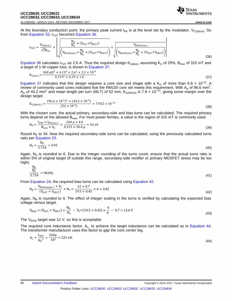
AL = LPRI
NP
2 =
txrJ
342= 225 nH
VBIAS = :VOUT + VRECT; × NB
NS
F VF=:19.5 + 0.45; × 4
6 F 0.7 = 12.6 V
NB = VBIAS:target ; + VF
:VOUT + VRECT; × NS =
12 + 0.7
19.5 + 0.45 × 6 = 3.82
NP
NS
5.734 = 98.8%
NS = NP
5.734 = 5.93
NP = LPRI × IPK:max ;
Bmax × Ae
= txrJ× 4.0
0.315 × 96.6 J = 34.18
KG:RM10 ; = (96.6 × 10⁻⁶)2 × (44.2 × 10-6)
(52 × 10-3) = 7.932 × 10⁻¹²
KG:des ;=txrJH
2 × 4.13
2 × 2.6
2 × 2.2 × 10
-8
0.3152 × 0.25 × 1.0
ITOT = VCS:bcm ;¾3RCS
×
ÏÎÎÎͪ NP
NS
× :VOUT+VRECT;FVBULK:min ;+ NP
NS
× :VOUT+VRECT;G+© VBULK:min ;
FVBULK:min ;+ NP
NS
× :VOUT+VRECT;GÒÑÑÑÐ
60
UCC28630, UCC28631UCC28632, UCC28633, UCC28634SLUSBW3D –MARCH 2014–REVISED DECEMBER 2017 www.ti.com
Product Folder Links: UCC28630 UCC28631 UCC28632 UCC28633 UCC28634
Submit Documentation Feedback Copyright © 2014–2017, Texas Instruments Incorporated
At the boundary conduction point, the primary peak current IPK is at the level set by the modulator, VCS(bcm). Sofrom Equation 33, ITOT becomes Equation 36.
(36)
Equation 36 calculates ITOT as 2.6 A. Thus the required design KG(des), assuming KU of 25%, Bmax of 315 mT anda target of 1-W copper loss, is shown in Equation 37.
(37)
Equation 37 indicates that this design requires a core size and shape with a KG of more than 6.9 × 10⁻¹². Areview of commonly used cores indicated that the RM10/I core set meets this requirement. With Ae of 96.6 mm2,Aw of 44.2 mm2 and mean length per turn (MLT) of 52 mm, KG(RM10) is 7.9 × 10⁻¹², giving some margin over thedesign target.
(38)
With the chosen core, the actual primary, secondary-side and bias turns can be calculated. The required primaryturns depend on the allowed Bmax. For most power ferrites, a value in the region of 315 mT is commonly used.
(39)
Round NP to 34. Now the required secondary-side turns can be calculated, using the previously calculated turnsratio per Equation 23.
(40)
Again, NS is rounded to 6. Due to the integer rounding of the turns count, ensure that the actual turns ratio iswithin 5% of original target (if outside this range, secondary-side rectifier or primary MOSFET stress may be toohigh).
(41)
From Equation 24, the required bias turns can be calculated using Equation 42.
(42)
Again, NB is rounded to 4. The effect of integer scaling in the turns is verified by calculating the expected biasvoltage versus target.
(43)
The VBIAS target was 12 V, so this is acceptable.
The required core inductance factor, AL, to achieve the target inductance can be calculated as in Equation 44.The transformer manufacturer uses this factor to gap the core center leg.
(44)
lg = F342 × vN × 10F7 × 102.31 J
260 JG F l44.6 m
5500×
102.31 J
96.6 Jp LwxuärJm
lg =F NP
2 × J0 × Ag
LPRI
G F llm
Jr
× Ag
Ae
p
Ag = ACENTRE × F1+lg
DCENTRE
G2
LuäuJ × l1+0.514
10.9p
2
= 102.31 mm2
lg = 342 × vN× 10-7 × 93.3 J
txrJF
44.6 m
5500 LwsvJm
lg = NP
2 × J0 × ACENTRE
LPRI
Flm
Jr
61
UCC28630, UCC28631UCC28632, UCC28633, UCC28634
www.ti.com SLUSBW3D –MARCH 2014–REVISED DECEMBER 2017
Product Folder Links: UCC28630 UCC28631 UCC28632 UCC28633 UCC28634
Submit Documentation FeedbackCopyright © 2014–2017, Texas Instruments Incorporated
Finally, calculate the required air-gap length lg, based on the required inductance and the core geometry.
where• μ0 is the permittivity of free-air• μr is the relative permeability of the chosen core ferrite material• ACENTRE is the cross-sectional area of the core center leg• lm is the core average magnetic path length (45)
For the RM10/I core in 3C95 material (chosen for low core loss over a wide temperature range), the required air-gap length is calaulated using Equation 46.
(46)
Typically, the air-gap calculation in Equation 45 underestimates lg, due to flux fringing in the air-gap. The fringingcauses the affective area of the air-gap Ag to be somewhat larger than the ferrite core center leg ACENTRE,depending on the gap length. This difference requires an increase in the required air-gap length to get therequired inductance, which results in a further increase in fringing. However use Equation 45 to determine aninitial value for lg, which can then be used to estimate Ag. For round centre legs, the increase in effective areawithin the gap can be estimated empirically from Equation 47
where• DCENTRE is the center leg diameter (47)
(For more information about this subject, download the paper Inductor and Flyback Transformer Design, LloydDixon, TI Power Supply Design Seminar SLUP127).
Because Equation 45 assumes that Ag equals ACENTRE, it must be modified using Equation 48.
(48)
Re-iterating the air-gap calculation in Equation 49 .
(49)
Typically, after the second iteration above in Equation 48, the estimated air-gap is very close to the requiredvalue. Further iterations can be made, but should not be necessary.
IPRI:rms ; = VCS:bcm ;¾3RCS
× ª NP
NS
× :VOUT + VRECT;FVBULK:min ; +
NP
NS
× :VOUT + VRECT;G =
0.64
¾3®0.2 × ¾0.58 = 1.41 A
VDS:max ; = VAC:pk _max ;+NP
NS
× :VOUT + VRECT; = 373 + 34
6 × 19.95 = 486 V
VRECT:rev ; = lNS
NP
× VAC:pk _max ;p + :VOUT + VRECT; = 6
34 × 373 + 19.95 = 85.8 V
VCS (slope ) = 50% × dBULK:min ; × RCS × nNS
NP × :VOUT + VRECT;
LPRI
r= 0.5 × 0.635 × 0.2 × F34 6¤ × 19.95
txrJG = 27.6 mV/Js
dBULK:min ; =
NP
NS
× :VOUT + VRECT;FVBULK:min ; +
NP
NS
× :VOUT + VRECT;G =
34 6 × :19.95;¤
:65 + 34 6 × :19.95;¤ ; = 63.5%
62
UCC28630, UCC28631UCC28632, UCC28633, UCC28634SLUSBW3D –MARCH 2014–REVISED DECEMBER 2017 www.ti.com
Product Folder Links: UCC28630 UCC28631 UCC28632 UCC28633 UCC28634
Submit Documentation Feedback Copyright © 2014–2017, Texas Instruments Incorporated
9.2.4.8 Slope Compensation VerificationAfter choosing the current sense resistor, transformer inductance and transformer turns ratio, verify the requiredslope compensation against the fixed internal slope compensation. The worst case slope compensationrequirement always occurs at the highest duty cycle operating point (at minimum bulk voltage level).
For stability, the slope compensation should be at least 50% of the difference between the inductor up-slope anddown-slope. [reference Bob Mammano TI Power Supply Design Seminar paper, 2001, SLUP173]. For a flybackconverter, the difference in slopes in CCM is equal the operating duty cycle multiplied by the inductor currentdown-slope value. For example, for 50% dBULK(min) at minimum bulk capacitor voltage, the required slopecompensation ramp is 25% of the inductor current down-slope.
As listed in Table 7, the specified peak-load transient is 130 W for 2 ms. In a worst case, peak transient timingwith respect to the AC phase, the VBULK minimum level dips to 65 V. This corresponds to a duty cycle ofapproximately 63.5% according to Equation 50.
(50)
The required slope compensation ramp is calculated at 63.5% duty cycle.
(51)
This value is within the 30 mV/μs of internal slope compensation provided by the controller.
9.2.4.9 Power MOSFET and Output Rectifier SelectionThe initial design target proposed the use of a 100-V Schottky rectifier. The secondary-side reverse voltagestress can be verified using the final transformer design sh own in Equation 52.
(52)
The value derived from Equation 52 is close to the original design target of 85 V.
For 65-W load, the average DC output current is 3.35 A for 19.5-V output. However, to reduce losses, a muchhigher current rated diode is typically used, to yield a much lower forward voltage drop VRECT. As shown inFigure 44, a 30-A rated diode D7 is used in this case, with a forward drop of approximately 0.45 V at 3.5 A,100°C.
For the primary-side MOSFET, the peak voltage stress can be estimated using Equation 53.
(53)
An allowance of at least 100 V must be added to this figure to account for the leakage inductance spike at turn-off. This voltage spike depends on the transformer implementation and the amount of leakage inductance, aswell as the specific design of the snubber. A more aggressive snubber may reduce the voltage spike, but at theexpense of higher losses in the snubber. A voltage rating of at least 600 V is recommended for the powerMOSFET to allow for leakage.
The MOSFET rms current at low line, rated load, can be estimated using Equation 54.
(54)
As can be seen in Figure 44, the chosen MOSFET Q1 is a 13-A, 600-V device.
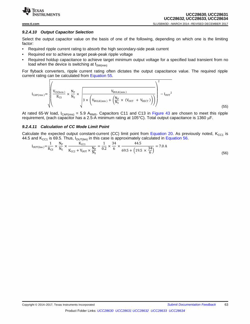
IOUT:lim ;=1
RCS
× NP
NS
× KCC1
KCC2 + VOUT × NP
NS
= 1
0.2 ×
34
6 ×
44.5
69.5 + @19.5 × 34
6A
= 7.0 A
ICAP:rms ;=
ã333333333333
ÉÈÈÈÇVCS:bcm ;
RCS
× NP
NS
× ª VBULK:min ;3 × mVBULK:min ; + FNP
NS
× :VOUT + VRECT ;GqÌËËËÊ
2
F IOUT2
63
UCC28630, UCC28631UCC28632, UCC28633, UCC28634
www.ti.com SLUSBW3D –MARCH 2014–REVISED DECEMBER 2017
Product Folder Links: UCC28630 UCC28631 UCC28632 UCC28633 UCC28634
Submit Documentation FeedbackCopyright © 2014–2017, Texas Instruments Incorporated
9.2.4.10 Output Capacitor SelectionSelect the output capacitor value on the basis of one of the following, depending on which one is the limitingfactor:• Required ripple current rating to absorb the high secondary-side peak current• Required esr to achieve a target peak-peak ripple voltage• Required holdup capacitance to achieve target minimum output voltage for a specified load transient from no
load when the device is switching at fSW(min)
For flyback converters, ripple current rating often dictates the output capacitance value. The required ripplecurrent rating can be calculated from Equation 55.
(55)
At rated 65-W load, ICAP(rms) = 5.9 ARMS. Capacitors C11 and C13 in Figure 43 are chosen to meet this ripplerequirement, (each capacitor has a 2.5-A minimum rating at 105°C). Total output capacitance is 1360 μF.
9.2.4.11 Calculation of CC Mode Limit PointCalculate the expected output constant-current (CC) limit point from Equation 20. As previously noted, KCC1 is44.5 and KCC1 is 69.5. Thus, IOUT(lim) in this case is approximately calculated in Equation 56.
(56)
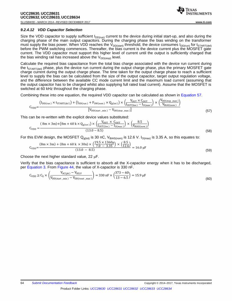
CVDD RCX × F VAC:pk; F VSELV
VDD:start _min ; FVDD:reset _max ;G = 330 nF × l373F 60
13F 6.5p = 15.9 JF
CVDD=
:8m × 3m; + :8m + 60 k × 30n; × @19.5 × suxrJ
7.0 F 3.35A × @ 8.5
12.6A
:13.0 F 8.5; LsxärJF
CVDD =
: 8m × 3m;+k8m + 60 k × Qg:PKP ;o × l VOUT × COUT
IOUT:HEI ; F IO:I=T ;p × l 8.5
VBIAS:JKI ;p
:13.0F 8.5;
CVDD=
kIDD:run ; × tSTART:del ;o + kIDD:run ; + FSW:nom ; × Qg:tot ;o × l VOUT × COUT
IOUT:lim ; F IO:max ;p × lVDD:stop _max ;
VBIAS:nom ;p
cVDD:start _min ; F VDD:stop _max ;g
64
UCC28630, UCC28631UCC28632, UCC28633, UCC28634SLUSBW3D –MARCH 2014–REVISED DECEMBER 2017 www.ti.com
Product Folder Links: UCC28630 UCC28631 UCC28632 UCC28633 UCC28634
Submit Documentation Feedback Copyright © 2014–2017, Texas Instruments Incorporated
9.2.4.12 VDD Capacitor SelectionSize the VDD capacitor to supply sufficient IDD(run) current to the device during initial start-up, and also during thecharging phase of the main output capacitors. During the charging phase the bias winding on the transformermust supply the bias power. When VDD reaches the VDD(start) threshold, the device consumes IDD(run) for tSTART(del)before the PWM switching commences. Thereafter, the bias current is the device current plus the MOSFET gatecurrent. The VDD capacitor must support this higher level of current until the output is sufficiently charged thatthe bias winding rail has increased above the VDD(stop) level.
Calculate the required bias capacitance from the total bias charge associated with the device run current duringthe tSTART(del) phase, plus the device run current during the output charge phase, plus the primary MOSFET gatecharge current during the output charge phase. The time taken for the output charge phase to reach a sufficientlevel to supply the bias can be calculated from the size of the output capacitor, target output regulation voltage,and the difference between the available CC mode current limit and the maximum load current (assuming thatthe output capacitor has to be charged whilst also supplying full rated load current). Assume that the MOSFET isswitched at 60 kHz throughout the charging phase.
Combining these into one equation, the required VDD capacitor can be calculated as shown in Equation 57.
(57)
This can be re-written with the explicit device values substituted:
(58)
For this EVM design, the MOSFET Qg(tot) is 30 nC, VBIAS(nom) is 12.6 V. IO(max) is 3.35 A, so this equates to:
(59)
Choose the next higher standard value, 22 μF.
Verify that the bias capacitance is sufficient to absorb all the X-capacitor energy when it has to be discharged,per Equation 3. From Figure 44, the value of X-capacitor is 330 nF.
(60)
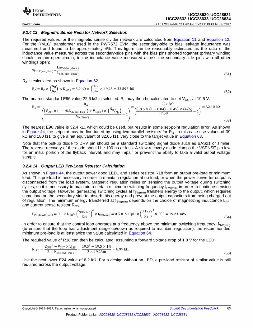
RLED = VOUT
2F VOUT × VLED
2 × P:preload _min ;=
19.52F 19.5 × 1.8
2 × 19.23m = 8.97 k3
PPRELOAD:min ; = 0.5 × LPRI× lVCS:min ;
RCS
p2
× fSW:min ; = 0.5 × 260 JH ×l0.172
0.2p
2
× 200 = 19.23 mW
RB = RA
LkVOUT × k1F%LLK:sec _bias ;o + VRECTo × @NBNSW A
VOUT:ref ; F 1M=
22.6 k3
l:19.5 × :1F 0.04; + 0.45; × :4 6¤ ;7.50
F 1p = 32.10 k3
RA = RP × lNB
NP
p × KLINE = 3.9 k3× l 4
34p × 49.25 = 22.597 k3
%LLK:sec _bias ;=LSEC:bias _short ;
LSEC:bias _open ;
65
UCC28630, UCC28631UCC28632, UCC28633, UCC28634
www.ti.com SLUSBW3D –MARCH 2014–REVISED DECEMBER 2017
Product Folder Links: UCC28630 UCC28631 UCC28632 UCC28633 UCC28634
Submit Documentation FeedbackCopyright © 2014–2017, Texas Instruments Incorporated
9.2.4.13 Magnetic Sense Resistor Network SelectionThe required values for the magnetic sense divider network are calculated from Equation 11 and Equation 12.For the RM10/I transformer used in the PWR572 EVM, the secondary-side to bias leakage inductance wasmeasured and found to be approximately 4%. This figure can be reasonably estimated as the ratio of theinductance value measured across the secondary-side pins with the bias pins shorted together (primary windingshould remain open-circuit), to the inductance value measured across the secondary-side pins with all otherwindings open:
(61)
RA is calculated as shown in Equation 62.
(62)
The nearest standard E96 value 22.6 kΩ is selected. RB may then be calculated to set VOUT at 19.5 V.
(63)
The nearest E96 value is 32.4 kΩ, which could be used, but results in some set-point regulation error. As shownin Figure 44, the setpoint may be fine-tuned by using two parallel resistors for RB. In this case use values of 39kΩ and 180 kΩ, to give a net equivalent of 32.05 kΩ, very close to the target value in Equation 63.
Note that the pull-up diode to DRV pin should be a standard switching signal diode such as BAS21 or similar.The reverse recovery of the diode should be 100 ns or less. A slow-recovery diode clamps the VSENSE pin lowfor an initial portion of the flyback interval, and may impair or prevent the ability to take a valid output voltagesample.
9.2.4.14 Output LED Pre-Load Resistor CalculationAs shown in Figure 44, the output power good LED1 and series resistor R18 form an output pre-load or minimumload. This pre-load is necessary in order to maintain regulation at no load, or when the power converter output isdisconnected from the load system. Magnetic regulation relies on sensing the output voltage during switchingcycles, so it is necessary to maintain a certain minimum switching frequency fSW(min) in order to continue sensingthe output voltage. However, generating switching cycles at fSW(min) transfers energy to the output, which requiressome load on the secondary-side to absorb this energy and prevent the output capacitors from being charged outof regulation. The minimum energy transferred at fSW(min) depends on the choice of magnetizing inductance LPRIand current sense resistor RCS.
(64)
In order to ensure that the control loop operates at a frequency above the minimum switching frequency, fSW(min)(to ensure that the loop has adjustment range up/down as required to maintain regulation), the recommendedminimum pre-load is at least twice the value calculated in Equation 64.
The required value of R18 can then be calculated, assuming a forward voltage drop of 1.8 V for the LED:
(65)
Use the next lower E24 value of 8.2 kΩ. For a design without an LED, a pre-load resistor of similar value is stillrequired across the output voltage.
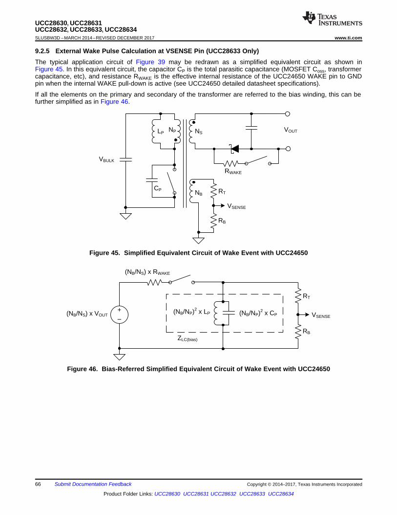
(NB/NS) x RWAKE
(NB/NP)2 x LP
RT
RB
VSENSE+±
(NB/NP)2 x CP
ZLC(bias)
(NB/NS) x VOUT
VOUT
RWAKE
VBULK
LP
CP
NP NS
NB RT
RB
VSENSE
66
UCC28630, UCC28631UCC28632, UCC28633, UCC28634SLUSBW3D –MARCH 2014–REVISED DECEMBER 2017 www.ti.com
Product Folder Links: UCC28630 UCC28631 UCC28632 UCC28633 UCC28634
Submit Documentation Feedback Copyright © 2014–2017, Texas Instruments Incorporated
9.2.5 External Wake Pulse Calculation at VSENSE Pin (UCC28633 Only)The typical application circuit of Figure 39 may be redrawn as a simplified equivalent circuit as shown inFigure 45. In this equivalent circuit, the capacitor CP is the total parasitic capacitance (MOSFET Coss, transformercapacitance, etc), and resistance RWAKE is the effective internal resistance of the UCC24650 WAKE pin to GNDpin when the internal WAKE pull-down is active (see UCC24650 detailed datasheet specifications).
If all the elements on the primary and secondary of the transformer are referred to the bias winding, this can befurther simplified as in Figure 46.
Figure 45. Simplified Equivalent Circuit of Wake Event with UCC24650
Figure 46. Bias-Referred Simplified Equivalent Circuit of Wake Event with UCC24650
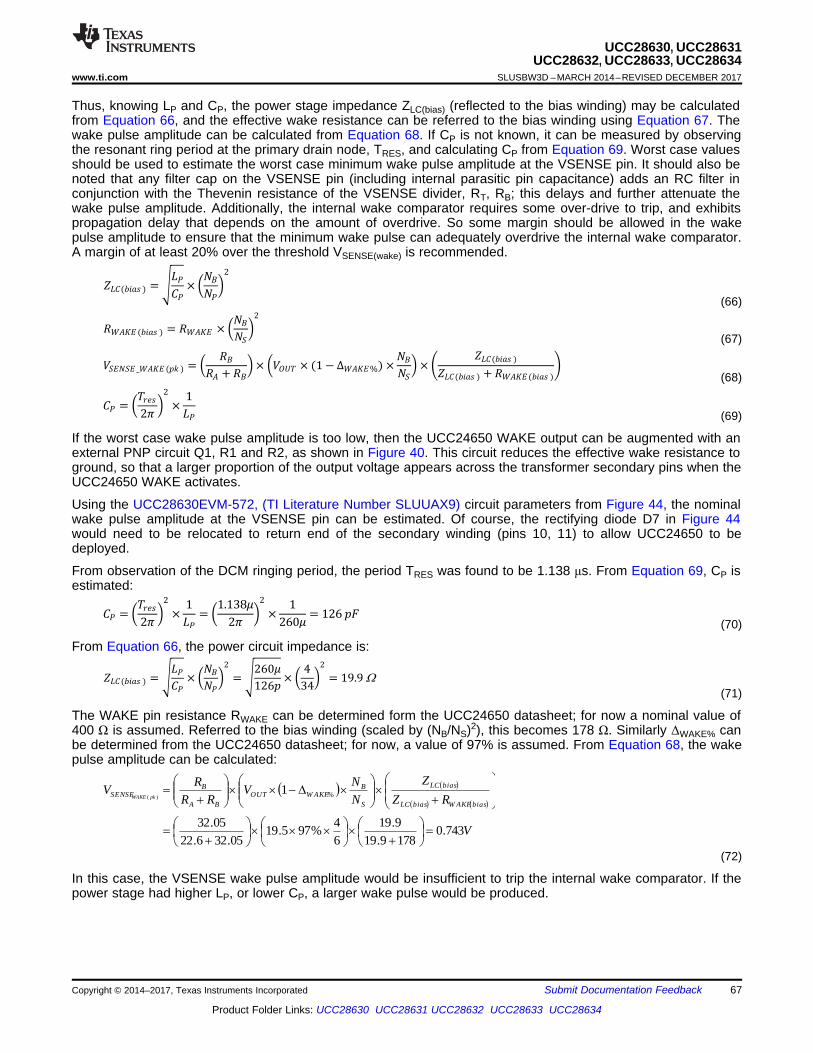
V
RZ
Z
N
NV
RR
RV
biasW AKEbiasLC
biasLC
S
BW AKEOUT
BA
BSENSE pkWAKE
743.01789.19
9.19
6
4%975.19
05.326.22
05.32
1 %)(
¸¹
ᬩ
§
u¸¹
ᬩ
§ uuu¸¹
ᬩ
§
¸¸¹
·¨¨©
§
u¸¹
ᬩ
§u'uu¸
¹
ᬩ
§
<.%(>E=O ) = ¨.2%2
× l0$02p2
= ¨260ä
126L× l 4
34p2
= 19.9 :
%2 = l6NAO2è
p2
×1
.2= l1.138ä
2èp
2
×1
260ä= 126 L(
%2 = l6NAO2è
p2
×1
.2
85'05'_9#-' (LG ) = l 4$
4# + 4$p× l8176 × (1F ¿9#-'%) ×0$
05p× F <.%(>E=O )
<.%(>E=O ) + 49#-'(>E=O )G
49#-' (>E=O ) = 49#-' × l0$05p2
<.%(>E=O ) =¨.2%2× l0$
02p2
67
UCC28630, UCC28631UCC28632, UCC28633, UCC28634
www.ti.com SLUSBW3D –MARCH 2014–REVISED DECEMBER 2017
Product Folder Links: UCC28630 UCC28631 UCC28632 UCC28633 UCC28634
Submit Documentation FeedbackCopyright © 2014–2017, Texas Instruments Incorporated
Thus, knowing LP and CP, the power stage impedance ZLC(bias) (reflected to the bias winding) may be calculatedfrom Equation 66, and the effective wake resistance can be referred to the bias winding using Equation 67. Thewake pulse amplitude can be calculated from Equation 68. If CP is not known, it can be measured by observingthe resonant ring period at the primary drain node, TRES, and calculating CP from Equation 69. Worst case valuesshould be used to estimate the worst case minimum wake pulse amplitude at the VSENSE pin. It should also benoted that any filter cap on the VSENSE pin (including internal parasitic pin capacitance) adds an RC filter inconjunction with the Thevenin resistance of the VSENSE divider, RT, RB; this delays and further attenuate thewake pulse amplitude. Additionally, the internal wake comparator requires some over-drive to trip, and exhibitspropagation delay that depends on the amount of overdrive. So some margin should be allowed in the wakepulse amplitude to ensure that the minimum wake pulse can adequately overdrive the internal wake comparator.A margin of at least 20% over the threshold VSENSE(wake) is recommended.
(66)
(67)
(68)
(69)
If the worst case wake pulse amplitude is too low, then the UCC24650 WAKE output can be augmented with anexternal PNP circuit Q1, R1 and R2, as shown in Figure 40. This circuit reduces the effective wake resistance toground, so that a larger proportion of the output voltage appears across the transformer secondary pins when theUCC24650 WAKE activates.
Using the UCC28630EVM-572, (TI Literature Number SLUUAX9) circuit parameters from Figure 44, the nominalwake pulse amplitude at the VSENSE pin can be estimated. Of course, the rectifying diode D7 in Figure 44would need to be relocated to return end of the secondary winding (pins 10, 11) to allow UCC24650 to bedeployed.
From observation of the DCM ringing period, the period TRES was found to be 1.138 μs. From Equation 69, CP isestimated:
(70)
From Equation 66, the power circuit impedance is:
(71)
The WAKE pin resistance RWAKE can be determined form the UCC24650 datasheet; for now a nominal value of400 Ω is assumed. Referred to the bias winding (scaled by (NB/NS)2), this becomes 178 Ω. Similarly ΔWAKE% canbe determined from the UCC24650 datasheet; for now, a value of 97% is assumed. From Equation 68, the wakepulse amplitude can be calculated:
(72)
In this case, the VSENSE wake pulse amplitude would be insufficient to trip the internal wake comparator. If thepower stage had higher LP, or lower CP, a larger wake pulse would be produced.
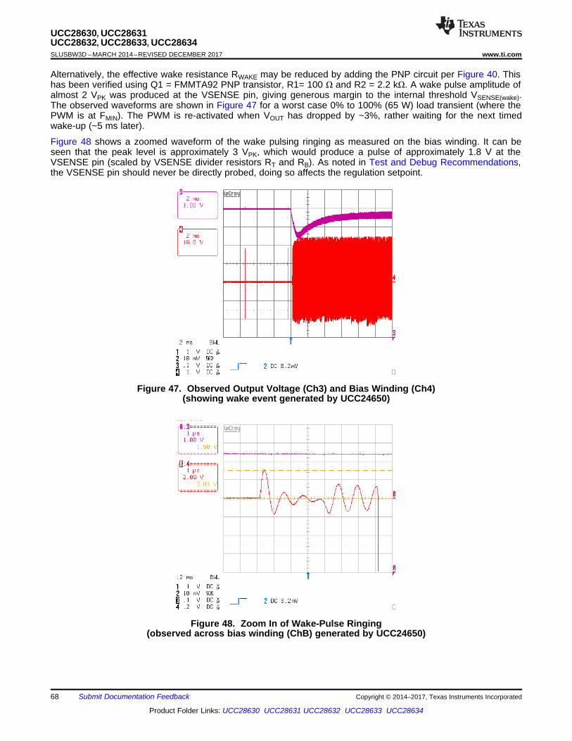
68
UCC28630, UCC28631UCC28632, UCC28633, UCC28634SLUSBW3D –MARCH 2014–REVISED DECEMBER 2017 www.ti.com
Product Folder Links: UCC28630 UCC28631 UCC28632 UCC28633 UCC28634
Submit Documentation Feedback Copyright © 2014–2017, Texas Instruments Incorporated
Alternatively, the effective wake resistance RWAKE may be reduced by adding the PNP circuit per Figure 40. Thishas been verified using Q1 = FMMTA92 PNP transistor, R1= 100 Ω and R2 = 2.2 kΩ. A wake pulse amplitude ofalmost 2 VPK was produced at the VSENSE pin, giving generous margin to the internal threshold VSENSE(wake).The observed waveforms are shown in Figure 47 for a worst case 0% to 100% (65 W) load transient (where thePWM is at FMIN). The PWM is re-activated when VOUT has dropped by ~3%, rather waiting for the next timedwake-up (~5 ms later).
Figure 48 shows a zoomed waveform of the wake pulsing ringing as measured on the bias winding. It can beseen that the peak level is approximately 3 VPK, which would produce a pulse of approximately 1.8 V at theVSENSE pin (scaled by VSENSE divider resistors RT and RB). As noted in Test and Debug Recommendations,the VSENSE pin should never be directly probed, doing so affects the regulation setpoint.
Figure 47. Observed Output Voltage (Ch3) and Bias Winding (Ch4)(showing wake event generated by UCC24650)
Figure 48. Zoom In of Wake-Pulse Ringing(observed across bias winding (ChB) generated by UCC24650)
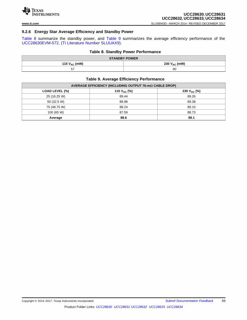
69
UCC28630, UCC28631UCC28632, UCC28633, UCC28634
www.ti.com SLUSBW3D –MARCH 2014–REVISED DECEMBER 2017
Product Folder Links: UCC28630 UCC28631 UCC28632 UCC28633 UCC28634
Submit Documentation FeedbackCopyright © 2014–2017, Texas Instruments Incorporated
9.2.6 Energy Star Average Efficiency and Standby PowerTable 8 summarize the standby power, and Table 9 summarizes the average efficiency performance of theUCC28630EVM-572, (TI Literature Number SLUUAX9).
Table 8. Standby Power PerformanceSTANDBY POWER
115 VAC (mW) 230 VAC (mW)57 60
Table 9. Average Efficiency PerformanceAVERAGE EFFICIENCY (INCLUDING OUTPUT 76-mΩ CABLE DROP)
LOAD LEVEL (%) 115 VAC (%) 230 VAC (%)25 (16.25 W) 89.44 89.2650 (32.5 W) 88.98 89.3875 (48.75 W) 88.24 89.10100 (65 W) 87.59 88.73Average 88.6 89.1
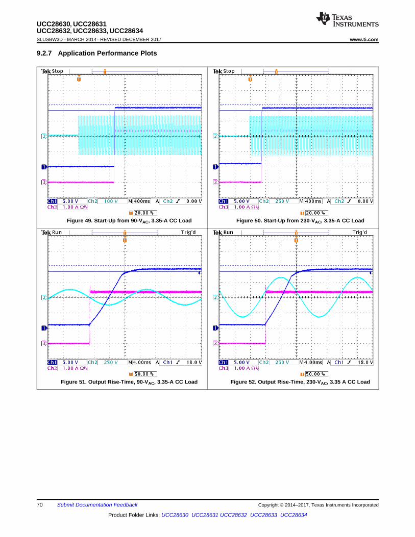
70
UCC28630, UCC28631UCC28632, UCC28633, UCC28634SLUSBW3D –MARCH 2014–REVISED DECEMBER 2017 www.ti.com
Product Folder Links: UCC28630 UCC28631 UCC28632 UCC28633 UCC28634
Submit Documentation Feedback Copyright © 2014–2017, Texas Instruments Incorporated
9.2.7 Application Performance Plots
Figure 49. Start-Up from 90-VAC, 3.35-A CC Load Figure 50. Start-Up from 230-VAC, 3.35-A CC Load
Figure 51. Output Rise-Time, 90-VAC, 3.35-A CC Load Figure 52. Output Rise-Time, 230-VAC, 3.35 A CC Load
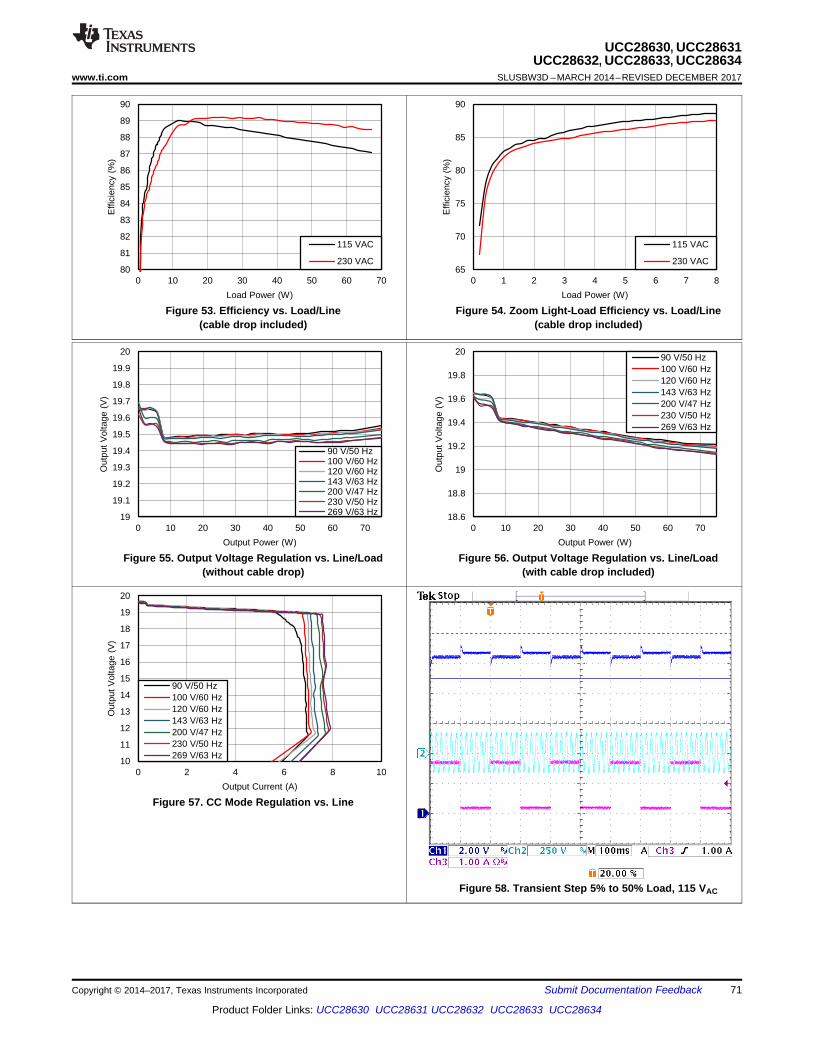
10
11
12
13
14
15
16
17
18
19
20
0 2 4 6 8 10
Out
put
Vol
tage
(V
)
Output Current (A)
90 V/50 Hz100 V/60 Hz120 V/60 Hz143 V/63 Hz200 V/47 Hz230 V/50 Hz269 V/63 Hz
C021
19
19.1
19.2
19.3
19.4
19.5
19.6
19.7
19.8
19.9
20
0 10 20 30 40 50 60 70
Out
put
Vol
tage
(V
)
Output Power (W)
90 V/50 Hz100 V/60 Hz120 V/60 Hz143 V/63 Hz200 V/47 Hz230 V/50 Hz269 V/63 Hz
C019
18.6
18.8
19
19.2
19.4
19.6
19.8
20
0 10 20 30 40 50 60 70
Out
put
Vol
tage
(V
)
Output Power (W)
90 V/50 Hz100 V/60 Hz120 V/60 Hz143 V/63 Hz200 V/47 Hz230 V/50 Hz269 V/63 Hz
C020
80
81
82
83
84
85
86
87
88
89
90
0 10 20 30 40 50 60 70
Effi
cien
cy (
%)
Load Power (W)
115 VAC
230 VAC
C017
65
70
75
80
85
90
0 1 2 3 4 5 6 7 8
Effi
cien
cy (
%)
Load Power (W)
115 VAC
230 VAC
C018
71
UCC28630, UCC28631UCC28632, UCC28633, UCC28634
www.ti.com SLUSBW3D –MARCH 2014–REVISED DECEMBER 2017
Product Folder Links: UCC28630 UCC28631 UCC28632 UCC28633 UCC28634
Submit Documentation FeedbackCopyright © 2014–2017, Texas Instruments Incorporated
Figure 53. Efficiency vs. Load/Line(cable drop included)
Figure 54. Zoom Light-Load Efficiency vs. Load/Line(cable drop included)
Figure 55. Output Voltage Regulation vs. Line/Load(without cable drop)
Figure 56. Output Voltage Regulation vs. Line/Load(with cable drop included)
Figure 57. CC Mode Regulation vs. Line
Figure 58. Transient Step 5% to 50% Load, 115 VAC
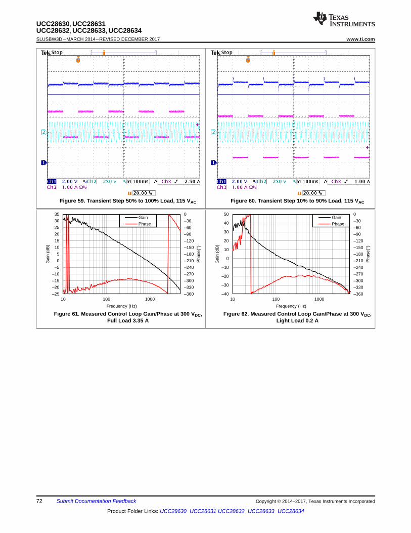
±360
±330
±300
±270
±240
±210
±180
±150
±120
±90
±60
±30
0
±25
±20
±15
±10
±5
0
5
10
15
20
25
30
35
10 100 1000
Pha
se(
)
Gai
n (d
B)
Frequency (Hz)
Gain
Phase
C022
±360
±330
±300
±270
±240
±210
±180
±150
±120
±90
±60
±30
0
±40
±30
±20
±10
0
10
20
30
40
50
10 100 1000
Pha
se(
)
Gai
n (d
B)
Frequency (Hz)
Gain
Phase
C023
72
UCC28630, UCC28631UCC28632, UCC28633, UCC28634SLUSBW3D –MARCH 2014–REVISED DECEMBER 2017 www.ti.com
Product Folder Links: UCC28630 UCC28631 UCC28632 UCC28633 UCC28634
Submit Documentation Feedback Copyright © 2014–2017, Texas Instruments Incorporated
Figure 59. Transient Step 50% to 100% Load, 115 VAC Figure 60. Transient Step 10% to 90% Load, 115 VAC
Figure 61. Measured Control Loop Gain/Phase at 300 VDC,Full Load 3.35 A
Figure 62. Measured Control Loop Gain/Phase at 300 VDC,Light Load 0.2 A

73
UCC28630, UCC28631UCC28632, UCC28633, UCC28634
www.ti.com SLUSBW3D –MARCH 2014–REVISED DECEMBER 2017
Product Folder Links: UCC28630 UCC28631 UCC28632 UCC28633 UCC28634
Submit Documentation FeedbackCopyright © 2014–2017, Texas Instruments Incorporated
9.3 Dos and Don'ts
9.3.1 Test and Debug RecommendationsOne important precaution must be noted during test and debug. Do not probe the VSENSE pin with anoscilloscope probe, meter or differential probe. Doing so adds excessive capacitance to the pin, delaying the pinrise-time, and causing the regulated system output voltage to increase.
10 Power Supply RecommendationsThe VDD power pin for the device requires the placement of low-esr noise-decoupling capacitance as directly aspossible from the VDD pin to the GND pin. Ceramic capacitors with stable dielectric characteristics overtemperature are recommended, such as X7R or better. Depending on the operating temperature range of theapplication, X5R may be acceptable, but the drop in capacitance value at high temperature and with applied DC-bias may not be tolerable. Avoid dielectrics with poor temperature-stability. (such Y5V, Z5U)
The recommended decoupling capacitors are a 1-μF 1206-sized 50-V X7R capacitor, ideally with (but notessential) a second smaller parallel 100-nF 0603-sized 50-V X7R capacitor. Higher voltage rating parts can alsobe used. The use of 25-V rated parts is not recommended, due to the reduction in effective capacitance valuewith applied DC bias.
In parallel with the ceramic noise-decoupling capacitor(s), a larger-capacitance energy storage capacitor is alsorequired, per Equation 58. This energy-storage capacitor does not require low esr, and does not necessarilyneed to be located close to the device.
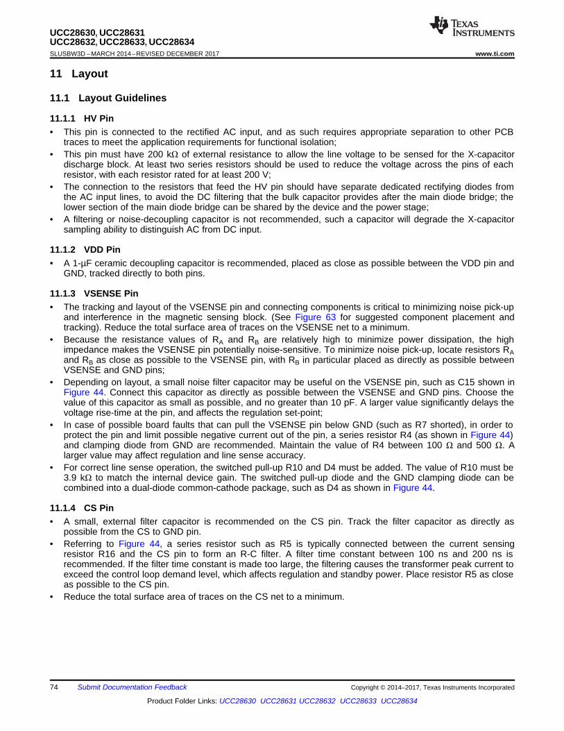
74
UCC28630, UCC28631UCC28632, UCC28633, UCC28634SLUSBW3D –MARCH 2014–REVISED DECEMBER 2017 www.ti.com
Product Folder Links: UCC28630 UCC28631 UCC28632 UCC28633 UCC28634
Submit Documentation Feedback Copyright © 2014–2017, Texas Instruments Incorporated
11 Layout
11.1 Layout Guidelines
11.1.1 HV Pin• This pin is connected to the rectified AC input, and as such requires appropriate separation to other PCB
traces to meet the application requirements for functional isolation;• This pin must have 200 kΩ of external resistance to allow the line voltage to be sensed for the X-capacitor
discharge block. At least two series resistors should be used to reduce the voltage across the pins of eachresistor, with each resistor rated for at least 200 V;
• The connection to the resistors that feed the HV pin should have separate dedicated rectifying diodes fromthe AC input lines, to avoid the DC filtering that the bulk capacitor provides after the main diode bridge; thelower section of the main diode bridge can be shared by the device and the power stage;
• A filtering or noise-decoupling capacitor is not recommended, such a capacitor will degrade the X-capacitorsampling ability to distinguish AC from DC input.
11.1.2 VDD Pin• A 1-µF ceramic decoupling capacitor is recommended, placed as close as possible between the VDD pin and
GND, tracked directly to both pins.
11.1.3 VSENSE Pin• The tracking and layout of the VSENSE pin and connecting components is critical to minimizing noise pick-up
and interference in the magnetic sensing block. (See Figure 63 for suggested component placement andtracking). Reduce the total surface area of traces on the VSENSE net to a minimum.
• Because the resistance values of RA and RB are relatively high to minimize power dissipation, the highimpedance makes the VSENSE pin potentially noise-sensitive. To minimize noise pick-up, locate resistors RAand RB as close as possible to the VSENSE pin, with RB in particular placed as directly as possible betweenVSENSE and GND pins;
• Depending on layout, a small noise filter capacitor may be useful on the VSENSE pin, such as C15 shown inFigure 44. Connect this capacitor as directly as possible between the VSENSE and GND pins. Choose thevalue of this capacitor as small as possible, and no greater than 10 pF. A larger value significantly delays thevoltage rise-time at the pin, and affects the regulation set-point;
• In case of possible board faults that can pull the VSENSE pin below GND (such as R7 shorted), in order toprotect the pin and limit possible negative current out of the pin, a series resistor R4 (as shown in Figure 44)and clamping diode from GND are recommended. Maintain the value of R4 between 100 Ω and 500 Ω. Alarger value may affect regulation and line sense accuracy.
• For correct line sense operation, the switched pull-up R10 and D4 must be added. The value of R10 must be3.9 kΩ to match the internal device gain. The switched pull-up diode and the GND clamping diode can becombined into a dual-diode common-cathode package, such as D4 as shown in Figure 44.
11.1.4 CS Pin• A small, external filter capacitor is recommended on the CS pin. Track the filter capacitor as directly as
possible from the CS to GND pin.• Referring to Figure 44, a series resistor such as R5 is typically connected between the current sensing
resistor R16 and the CS pin to form an R-C filter. A filter time constant between 100 ns and 200 ns isrecommended. If the filter time constant is made too large, the filtering causes the transformer peak current toexceed the control loop demand level, which affects regulation and standby power. Place resistor R5 as closeas possible to the CS pin.
• Reduce the total surface area of traces on the CS net to a minimum.
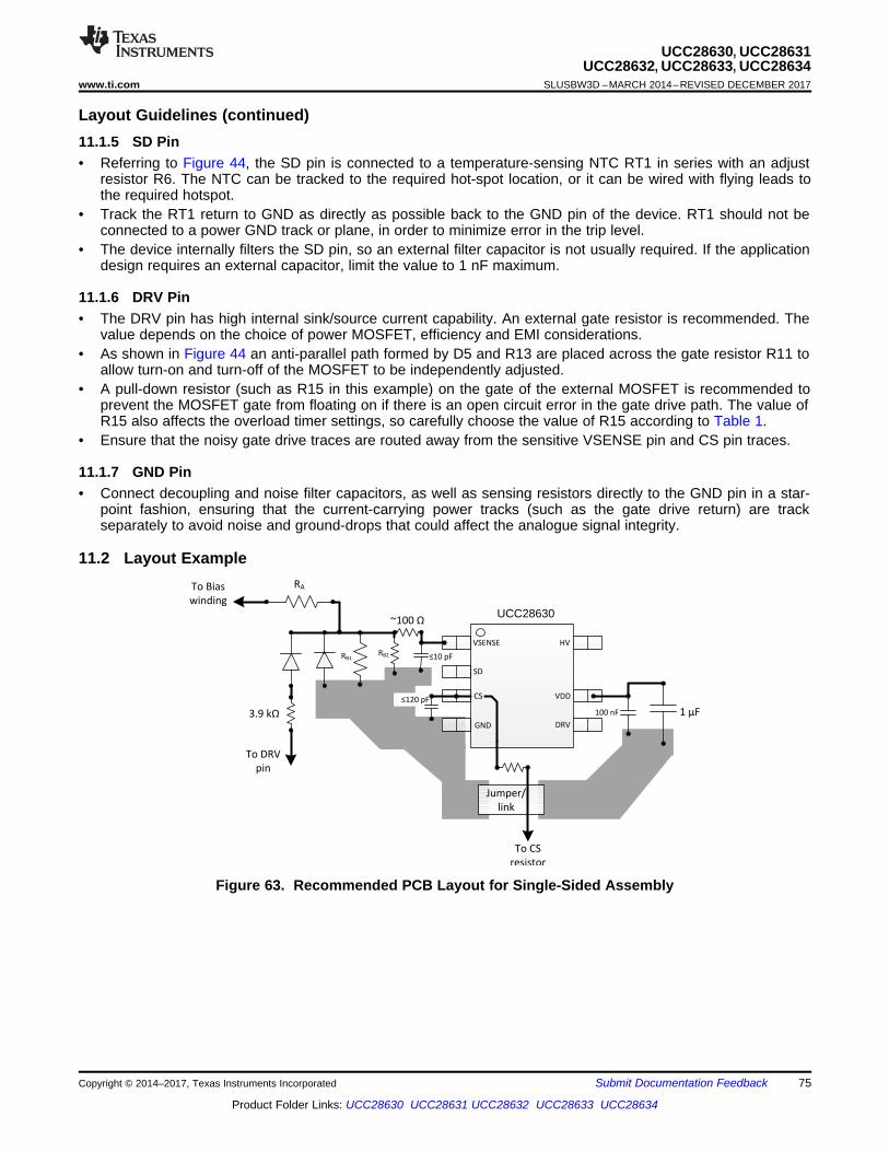
RA
RB1
~100 Q
To Bias
winding
To DRV
pin
3.9 lQ
Jumper/
link
To CS
resistor
VDD
DRV
HVVSENSE
SD
GND
1 µF100 nF
G10 pF
G120 pF CS
RB2
UCC28630
75
UCC28630, UCC28631UCC28632, UCC28633, UCC28634
www.ti.com SLUSBW3D –MARCH 2014–REVISED DECEMBER 2017
Product Folder Links: UCC28630 UCC28631 UCC28632 UCC28633 UCC28634
Submit Documentation FeedbackCopyright © 2014–2017, Texas Instruments Incorporated
Layout Guidelines (continued)11.1.5 SD Pin• Referring to Figure 44, the SD pin is connected to a temperature-sensing NTC RT1 in series with an adjust
resistor R6. The NTC can be tracked to the required hot-spot location, or it can be wired with flying leads tothe required hotspot.
• Track the RT1 return to GND as directly as possible back to the GND pin of the device. RT1 should not beconnected to a power GND track or plane, in order to minimize error in the trip level.
• The device internally filters the SD pin, so an external filter capacitor is not usually required. If the applicationdesign requires an external capacitor, limit the value to 1 nF maximum.
11.1.6 DRV Pin• The DRV pin has high internal sink/source current capability. An external gate resistor is recommended. The
value depends on the choice of power MOSFET, efficiency and EMI considerations.• As shown in Figure 44 an anti-parallel path formed by D5 and R13 are placed across the gate resistor R11 to
allow turn-on and turn-off of the MOSFET to be independently adjusted.• A pull-down resistor (such as R15 in this example) on the gate of the external MOSFET is recommended to
prevent the MOSFET gate from floating on if there is an open circuit error in the gate drive path. The value ofR15 also affects the overload timer settings, so carefully choose the value of R15 according to Table 1.
• Ensure that the noisy gate drive traces are routed away from the sensitive VSENSE pin and CS pin traces.
11.1.7 GND Pin• Connect decoupling and noise filter capacitors, as well as sensing resistors directly to the GND pin in a star-
point fashion, ensuring that the current-carrying power tracks (such as the gate drive return) are trackseparately to avoid noise and ground-drops that could affect the analogue signal integrity.
11.2 Layout Example
Figure 63. Recommended PCB Layout for Single-Sided Assembly

76
UCC28630, UCC28631UCC28632, UCC28633, UCC28634SLUSBW3D –MARCH 2014–REVISED DECEMBER 2017 www.ti.com
Product Folder Links: UCC28630 UCC28631 UCC28632 UCC28633 UCC28634
Submit Documentation Feedback Copyright © 2014–2017, Texas Instruments Incorporated
12 Device and Documentation Support
12.1 Device Support
12.1.1 Development Support
12.1.1.1 Custom Design With WEBENCH® ToolsClick here to create a custom design using the UCC2863x device with the WEBENCH® Power Designer.1. Start by entering the input voltage (VIN), output voltage (VOUT), and output current (IOUT) requirements.2. Optimize the design for key parameters such as efficiency, footprint, and cost using the optimizer dial.3. Compare the generated design with other possible solutions from Texas Instruments.
The WEBENCH Power Designer provides a customized schematic along with a list of materials with real-timepricing and component availability.
In most cases, these actions are available:• Run electrical simulations to see important waveforms and circuit performance• Run thermal simulations to understand board thermal performance• Export customized schematic and layout into popular CAD formats• Print PDF reports for the design, and share the design with colleagues
Get more information about WEBENCH tools at www.ti.com/WEBENCH.
12.2 Documentation Support
12.2.1 Related DocumentationUCC28630EVM-572, 65-W Nominal, 130-W Peak, Primary-Side Regulated Adapter Module (Texas InstrumentsLiterature Number SLUSAX9)
12.2.1.1 Related LinksThe table below lists quick access links. Categories include technical documents, support and communityresources, tools and software, and quick access to sample or buy.
Table 10. Related Links
PARTS PRODUCT FOLDER SAMPLE & BUY TECHNICALDOCUMENTS
TOOLS &SOFTWARE
SUPPORT &COMMUNITY
UCC28630 Click here Click here Click here Click here Click hereUCC28631 Click here Click here Click here Click here Click hereUCC28632 Click here Click here Click here Click here Click hereUCC28633 Click here Click here Click here Click here Click here
12.3 Receiving Notification of Documentation UpdatesTo receive notification of documentation updates, navigate to the device product folder on ti.com. In the upperright corner, click on Alert me to register and receive a weekly digest of any product information that haschanged. For change details, review the revision history included in any revised document.
12.4 Community ResourcesThe following links connect to TI community resources. Linked contents are provided "AS IS" by the respectivecontributors. They do not constitute TI specifications and do not necessarily reflect TI's views; see TI's Terms ofUse.
TI E2E™ Online Community TI's Engineer-to-Engineer (E2E) Community. Created to foster collaborationamong engineers. At e2e.ti.com, you can ask questions, share knowledge, explore ideas and helpsolve problems with fellow engineers.

77
UCC28630, UCC28631UCC28632, UCC28633, UCC28634
www.ti.com SLUSBW3D –MARCH 2014–REVISED DECEMBER 2017
Product Folder Links: UCC28630 UCC28631 UCC28632 UCC28633 UCC28634
Submit Documentation FeedbackCopyright © 2014–2017, Texas Instruments Incorporated
Community Resources (continued)Design Support TI's Design Support Quickly find helpful E2E forums along with design support tools and
contact information for technical support.
12.5 TrademarksE2E is a trademark of Texas Instruments.WEBENCH is a registered trademark of Texas Instruments.All other trademarks are the property of their respective owners.
12.6 Electrostatic Discharge CautionThis integrated circuit can be damaged by ESD. Texas Instruments recommends that all integrated circuits be handled withappropriate precautions. Failure to observe proper handling and installation procedures can cause damage.
ESD damage can range from subtle performance degradation to complete device failure. Precision integrated circuits may be moresusceptible to damage because very small parametric changes could cause the device not to meet its published specifications.
12.7 GlossarySLYZ022 — TI Glossary.
This glossary lists and explains terms, acronyms, and definitions.
13 Mechanical, Packaging, and Orderable InformationThe following pages include mechanical packaging and orderable information. This information is the mostcurrent data available for the designated devices. This data is subject to change without notice and revision ofthis document. For browser-based versions of this data sheet, refer to the left-hand navigation.
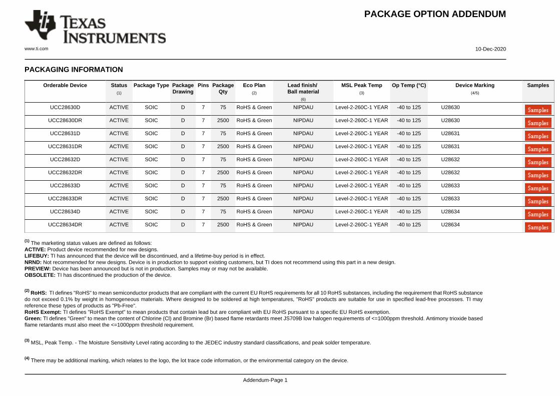
PACKAGE OPTION ADDENDUM
www.ti.com 10-Dec-2020
Addendum-Page 1
PACKAGING INFORMATION
Orderable Device Status(1)
Package Type PackageDrawing
Pins PackageQty
Eco Plan(2)
Lead finish/Ball material
(6)
MSL Peak Temp(3)
Op Temp (°C) Device Marking(4/5)
Samples
UCC28630D ACTIVE SOIC D 7 75 RoHS & Green NIPDAU Level-2-260C-1 YEAR -40 to 125 U28630
UCC28630DR ACTIVE SOIC D 7 2500 RoHS & Green NIPDAU Level-2-260C-1 YEAR -40 to 125 U28630
UCC28631D ACTIVE SOIC D 7 75 RoHS & Green NIPDAU Level-2-260C-1 YEAR -40 to 125 U28631
UCC28631DR ACTIVE SOIC D 7 2500 RoHS & Green NIPDAU Level-2-260C-1 YEAR -40 to 125 U28631
UCC28632D ACTIVE SOIC D 7 75 RoHS & Green NIPDAU Level-2-260C-1 YEAR -40 to 125 U28632
UCC28632DR ACTIVE SOIC D 7 2500 RoHS & Green NIPDAU Level-2-260C-1 YEAR -40 to 125 U28632
UCC28633D ACTIVE SOIC D 7 75 RoHS & Green NIPDAU Level-2-260C-1 YEAR -40 to 125 U28633
UCC28633DR ACTIVE SOIC D 7 2500 RoHS & Green NIPDAU Level-2-260C-1 YEAR -40 to 125 U28633
UCC28634D ACTIVE SOIC D 7 75 RoHS & Green NIPDAU Level-2-260C-1 YEAR -40 to 125 U28634
UCC28634DR ACTIVE SOIC D 7 2500 RoHS & Green NIPDAU Level-2-260C-1 YEAR -40 to 125 U28634
(1) The marketing status values are defined as follows:ACTIVE: Product device recommended for new designs.LIFEBUY: TI has announced that the device will be discontinued, and a lifetime-buy period is in effect.NRND: Not recommended for new designs. Device is in production to support existing customers, but TI does not recommend using this part in a new design.PREVIEW: Device has been announced but is not in production. Samples may or may not be available.OBSOLETE: TI has discontinued the production of the device.
(2) RoHS: TI defines "RoHS" to mean semiconductor products that are compliant with the current EU RoHS requirements for all 10 RoHS substances, including the requirement that RoHS substancedo not exceed 0.1% by weight in homogeneous materials. Where designed to be soldered at high temperatures, "RoHS" products are suitable for use in specified lead-free processes. TI mayreference these types of products as "Pb-Free".RoHS Exempt: TI defines "RoHS Exempt" to mean products that contain lead but are compliant with EU RoHS pursuant to a specific EU RoHS exemption.Green: TI defines "Green" to mean the content of Chlorine (Cl) and Bromine (Br) based flame retardants meet JS709B low halogen requirements of <=1000ppm threshold. Antimony trioxide basedflame retardants must also meet the <=1000ppm threshold requirement.
(3) MSL, Peak Temp. - The Moisture Sensitivity Level rating according to the JEDEC industry standard classifications, and peak solder temperature.
(4) There may be additional marking, which relates to the logo, the lot trace code information, or the environmental category on the device.

PACKAGE OPTION ADDENDUM
www.ti.com 10-Dec-2020
Addendum-Page 2
(5) Multiple Device Markings will be inside parentheses. Only one Device Marking contained in parentheses and separated by a "~" will appear on a device. If a line is indented then it is a continuationof the previous line and the two combined represent the entire Device Marking for that device.
(6) Lead finish/Ball material - Orderable Devices may have multiple material finish options. Finish options are separated by a vertical ruled line. Lead finish/Ball material values may wrap to twolines if the finish value exceeds the maximum column width.
Important Information and Disclaimer:The information provided on this page represents TI's knowledge and belief as of the date that it is provided. TI bases its knowledge and belief on informationprovided by third parties, and makes no representation or warranty as to the accuracy of such information. Efforts are underway to better integrate information from third parties. TI has taken andcontinues to take reasonable steps to provide representative and accurate information but may not have conducted destructive testing or chemical analysis on incoming materials and chemicals.TI and TI suppliers consider certain information to be proprietary, and thus CAS numbers and other limited information may not be available for release.
In no event shall TI's liability arising out of such information exceed the total purchase price of the TI part(s) at issue in this document sold by TI to Customer on an annual basis.
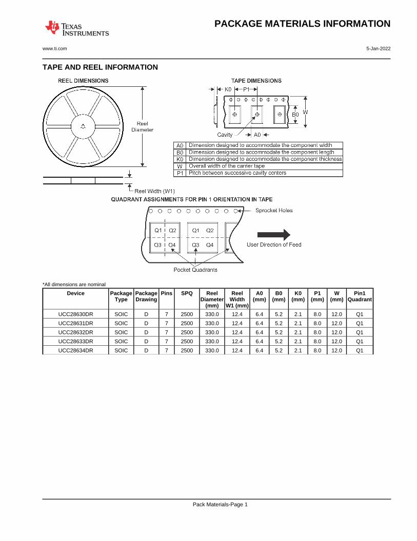
TAPE AND REEL INFORMATION
*All dimensions are nominal
Device PackageType
PackageDrawing
Pins SPQ ReelDiameter
(mm)
ReelWidth
W1 (mm)
A0(mm)
B0(mm)
K0(mm)
P1(mm)
W(mm)
Pin1Quadrant
UCC28630DR SOIC D 7 2500 330.0 12.4 6.4 5.2 2.1 8.0 12.0 Q1
UCC28631DR SOIC D 7 2500 330.0 12.4 6.4 5.2 2.1 8.0 12.0 Q1
UCC28632DR SOIC D 7 2500 330.0 12.4 6.4 5.2 2.1 8.0 12.0 Q1
UCC28633DR SOIC D 7 2500 330.0 12.4 6.4 5.2 2.1 8.0 12.0 Q1
UCC28634DR SOIC D 7 2500 330.0 12.4 6.4 5.2 2.1 8.0 12.0 Q1
PACKAGE MATERIALS INFORMATION
www.ti.com 5-Jan-2022
Pack Materials-Page 1
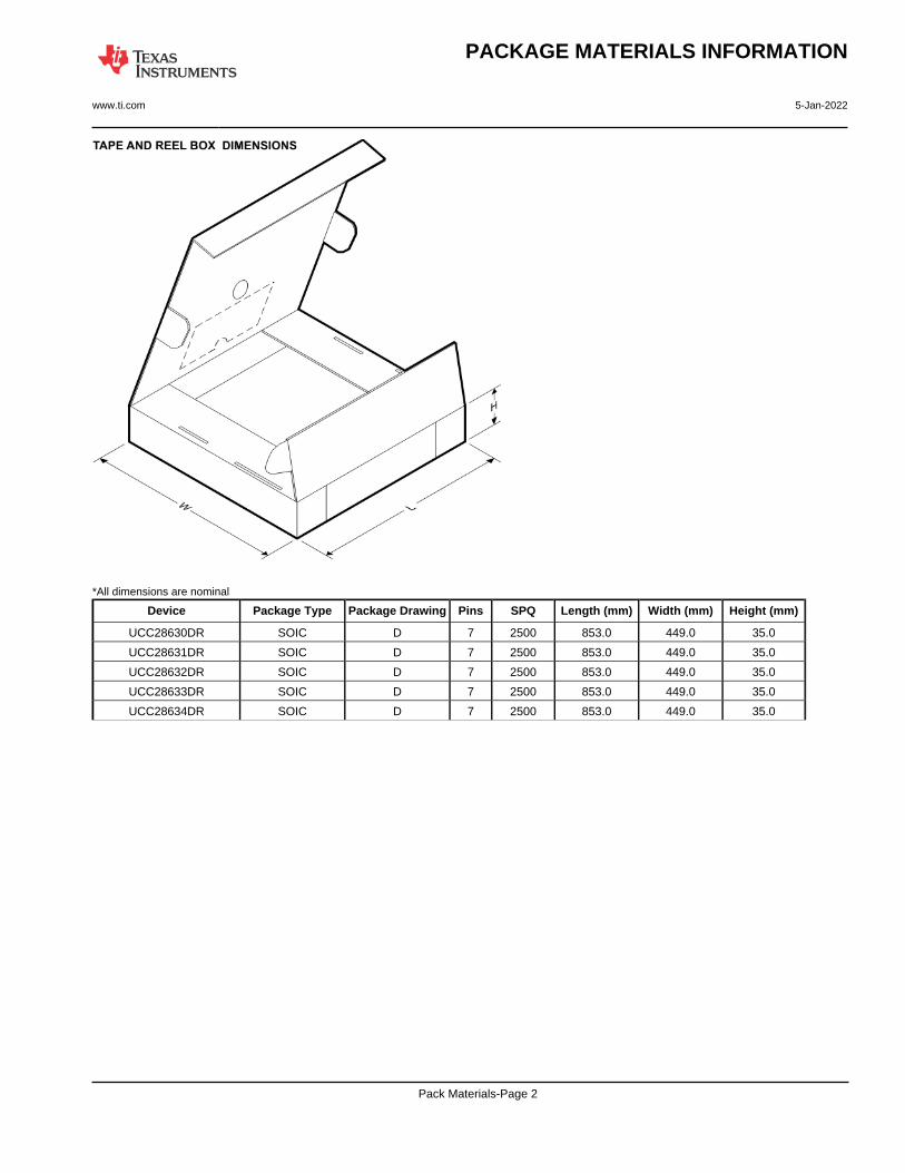
*All dimensions are nominal
Device Package Type Package Drawing Pins SPQ Length (mm) Width (mm) Height (mm)
UCC28630DR SOIC D 7 2500 853.0 449.0 35.0
UCC28631DR SOIC D 7 2500 853.0 449.0 35.0
UCC28632DR SOIC D 7 2500 853.0 449.0 35.0
UCC28633DR SOIC D 7 2500 853.0 449.0 35.0
UCC28634DR SOIC D 7 2500 853.0 449.0 35.0
PACKAGE MATERIALS INFORMATION
www.ti.com 5-Jan-2022
Pack Materials-Page 2
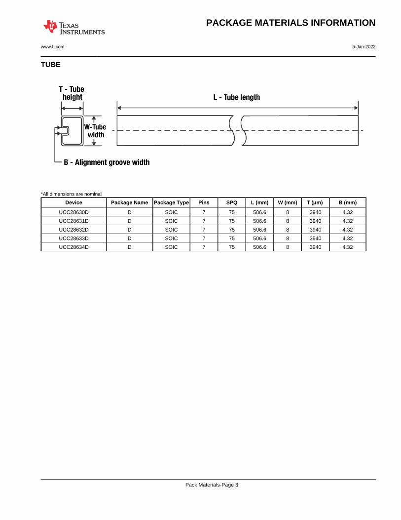
TUBE
*All dimensions are nominal
Device Package Name Package Type Pins SPQ L (mm) W (mm) T (µm) B (mm)
UCC28630D D SOIC 7 75 506.6 8 3940 4.32
UCC28631D D SOIC 7 75 506.6 8 3940 4.32
UCC28632D D SOIC 7 75 506.6 8 3940 4.32
UCC28633D D SOIC 7 75 506.6 8 3940 4.32
UCC28634D D SOIC 7 75 506.6 8 3940 4.32
PACKAGE MATERIALS INFORMATION
www.ti.com 5-Jan-2022
Pack Materials-Page 3
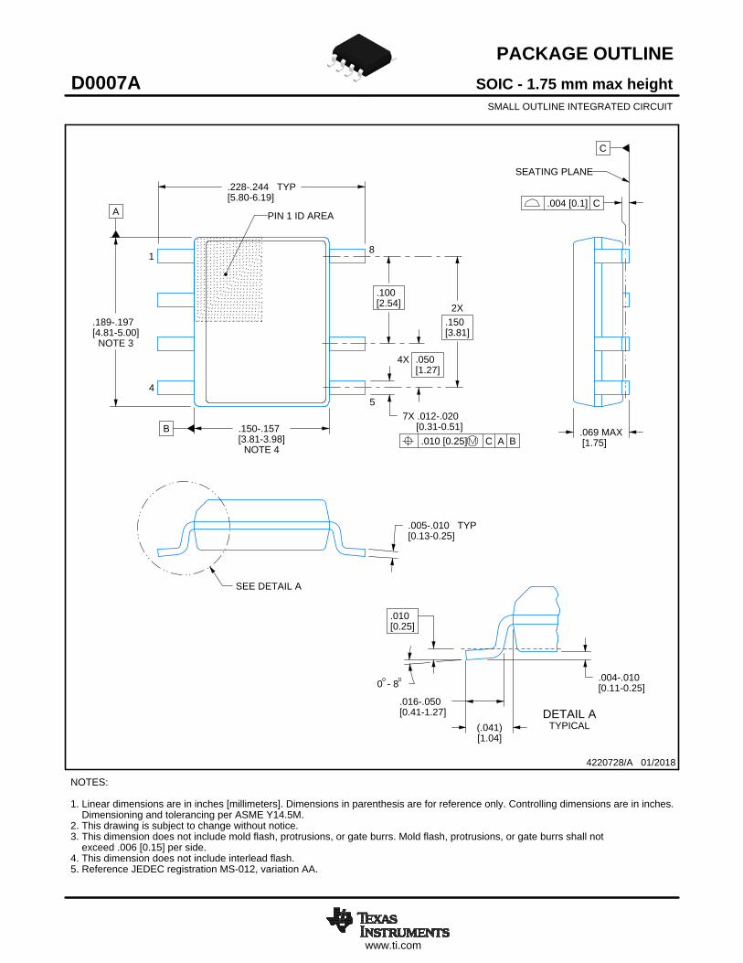
www.ti.com
PACKAGE OUTLINE
C
.228-.244 TYP[5.80-6.19]
.069 MAX[1.75]
.100[2.54]
7X .012-.020 [0.31-0.51]
2X.150[3.81]
.005-.010 TYP[0.13-0.25]
0 - 8 .004-.010[0.11-0.25]
.010[0.25]
.016-.050[0.41-1.27]
4X .050[1.27]
A
.189-.197[4.81-5.00]
NOTE 3
B .150-.157[3.81-3.98]
NOTE 4
(.041)[1.04]
SOIC - 1.75 mm max heightD0007ASMALL OUTLINE INTEGRATED CIRCUIT
4220728/A 01/2018
NOTES: 1. Linear dimensions are in inches [millimeters]. Dimensions in parenthesis are for reference only. Controlling dimensions are in inches. Dimensioning and tolerancing per ASME Y14.5M. 2. This drawing is subject to change without notice. 3. This dimension does not include mold flash, protrusions, or gate burrs. Mold flash, protrusions, or gate burrs shall not exceed .006 [0.15] per side. 4. This dimension does not include interlead flash.5. Reference JEDEC registration MS-012, variation AA.
18
.010 [0.25] C A B
54
PIN 1 ID AREA
SEATING PLANE
.004 [0.1] C
SEE DETAIL A
DETAIL ATYPICAL
SCALE 2.800
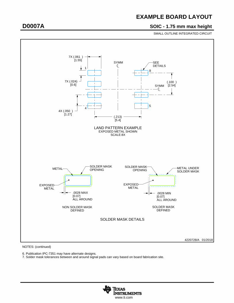
www.ti.com
EXAMPLE BOARD LAYOUT
.0028 MAX[0.07]ALL AROUND
.0028 MIN[0.07]ALL AROUND
(.213)[5.4]
4X (.050 )[1.27]
7X (.061 )[1.55]
7X (.024)[0.6]
(.100 )[2.54]
SOIC - 1.75 mm max heightD0007ASMALL OUTLINE INTEGRATED CIRCUIT
4220728/A 01/2018
NOTES: (continued) 6. Publication IPC-7351 may have alternate designs. 7. Solder mask tolerances between and around signal pads can vary based on board fabrication site.
METALSOLDER MASKOPENING
NON SOLDER MASKDEFINED
SOLDER MASK DETAILS
EXPOSEDMETAL
OPENINGSOLDER MASK METAL UNDER
SOLDER MASK
SOLDER MASKDEFINED
EXPOSEDMETAL
LAND PATTERN EXAMPLEEXPOSED METAL SHOWN
SCALE:8X
SYMM
1
45
8
SEEDETAILS
SYMM
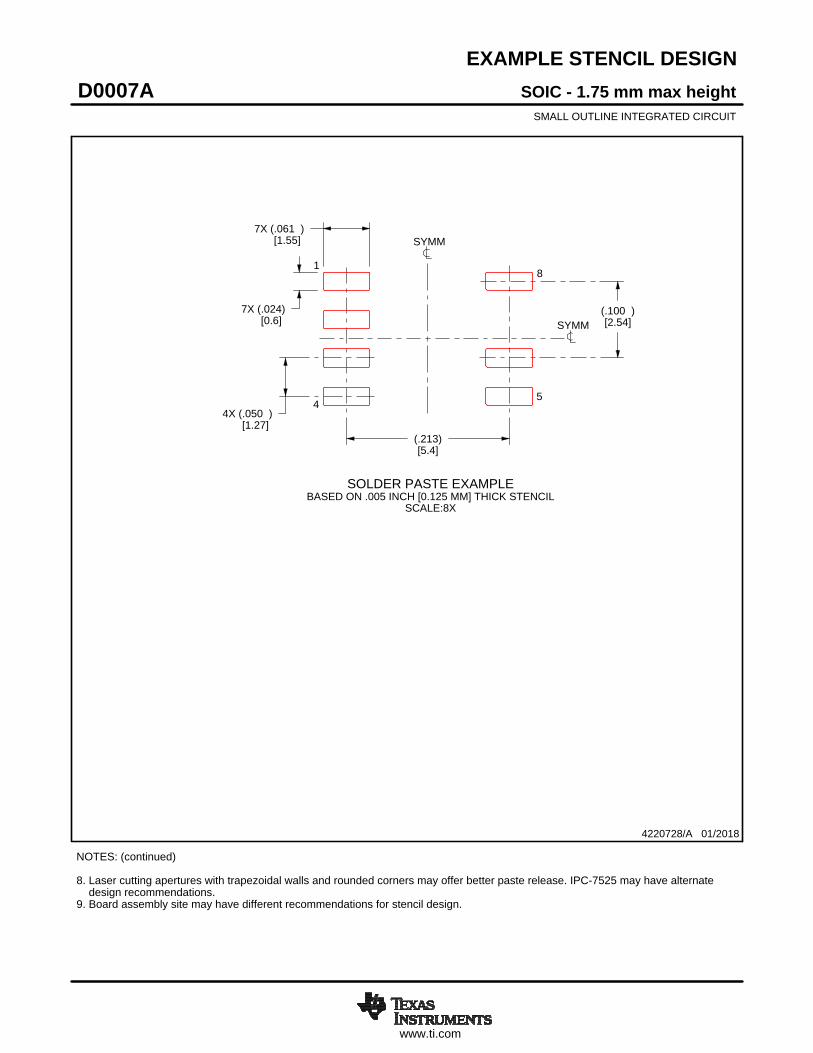
www.ti.com
EXAMPLE STENCIL DESIGN
7X (.061 )[1.55]
7X (.024)[0.6]
4X (.050 )[1.27]
(.213)[5.4]
(.100 )[2.54]
SOIC - 1.75 mm max heightD0007ASMALL OUTLINE INTEGRATED CIRCUIT
4220728/A 01/2018
NOTES: (continued) 8. Laser cutting apertures with trapezoidal walls and rounded corners may offer better paste release. IPC-7525 may have alternate design recommendations. 9. Board assembly site may have different recommendations for stencil design.
SOLDER PASTE EXAMPLEBASED ON .005 INCH [0.125 MM] THICK STENCIL
SCALE:8X
SYMM
SYMM
1
45
8

IMPORTANT NOTICE AND DISCLAIMERTI PROVIDES TECHNICAL AND RELIABILITY DATA (INCLUDING DATA SHEETS), DESIGN RESOURCES (INCLUDING REFERENCE DESIGNS), APPLICATION OR OTHER DESIGN ADVICE, WEB TOOLS, SAFETY INFORMATION, AND OTHER RESOURCES “AS IS” AND WITH ALL FAULTS, AND DISCLAIMS ALL WARRANTIES, EXPRESS AND IMPLIED, INCLUDING WITHOUT LIMITATION ANY IMPLIED WARRANTIES OF MERCHANTABILITY, FITNESS FOR A PARTICULAR PURPOSE OR NON-INFRINGEMENT OF THIRD PARTY INTELLECTUAL PROPERTY RIGHTS.These resources are intended for skilled developers designing with TI products. You are solely responsible for (1) selecting the appropriate TI products for your application, (2) designing, validating and testing your application, and (3) ensuring your application meets applicable standards, and any other safety, security, regulatory or other requirements.These resources are subject to change without notice. TI grants you permission to use these resources only for development of an application that uses the TI products described in the resource. Other reproduction and display of these resources is prohibited. No license is granted to any other TI intellectual property right or to any third party intellectual property right. TI disclaims responsibility for, and you will fully indemnify TI and its representatives against, any claims, damages, costs, losses, and liabilities arising out of your use of these resources.TI’s products are provided subject to TI’s Terms of Sale or other applicable terms available either on ti.com or provided in conjunction with such TI products. TI’s provision of these resources does not expand or otherwise alter TI’s applicable warranties or warranty disclaimers for TI products.TI objects to and rejects any additional or different terms you may have proposed. IMPORTANT NOTICE
Mailing Address: Texas Instruments, Post Office Box 655303, Dallas, Texas 75265Copyright © 2022, Texas Instruments Incorporated
Related Documents