UBI >> Contents Lecture 8 USCI Module SPI & I2C Mode MSP430 Teaching Materials Texas Instruments Incorporated University of Beira Interior (PT) Pedro Dinis Gaspar, António Espírito Santo, Bruno Ribeiro, Humberto Santos University of Beira Interior, Electromechanical Engineering Department www.msp430.ubi.pt Copyright 2009 Texas Instruments All Rights Reserved www.msp430.ubi.pt

Welcome message from author
This document is posted to help you gain knowledge. Please leave a comment to let me know what you think about it! Share it to your friends and learn new things together.
Transcript

UBI
>> Contents
Lecture 8USCI Module SPI & I2C Mode
MSP430 Teaching Materials
Texas Instruments IncorporatedUniversity of Beira Interior (PT)
Pedro Dinis Gaspar, António Espírito Santo, Bruno Ribeiro, Humberto Santos
University of Beira Interior, Electromechanical Engineering Departmentwww.msp430.ubi.pt
Copyright 2009 Texas Instruments All Rights Reserved
www.msp430.ubi.pt

UBI
>> Contents2
Copyright 2009 Texas Instruments All Rights Reserved
www.msp430.ubi.pt
Contents
USCI operation: SPI mode
USCI operation: I2C mode
USCI registers: UART, SPI and I2C modes

UBI
>> Contents3
Copyright 2009 Texas Instruments All Rights Reserved
www.msp430.ubi.pt
Serial Peripheral Interface (SPI) protocol (1/2)
The Serial Peripheral Interface ( SPI) bus is a standard form of synchronous serial communication;
Developed by Motorola;
Operates in full duplex mode;
Master/Slave relationship;
Communication is always initiated by the master. Low cost.

UBI
>> Contents4
Copyright 2009 Texas Instruments All Rights Reserved
www.msp430.ubi.pt
Peripheral Interface Serial (SPI) protocol (2/2)
Supports only one master;
Can support more than a slave;
Short distance between devices, e.g. on a printed circuit boards (PCBs);
Special attention needs to be observed to the polarity and phase of the clock signal;
The master sends data on one edge of clock and reads data on the other edge. Therefore, it can send/receive at the same time.

UBI
>> Contents5
Copyright 2009 Texas Instruments All Rights Reserved
www.msp430.ubi.pt
USCI operation: SPI mode (1/9)
Flexible interface: 3- or 4-pin SPI; 7- or 8-bit data length; Master or slave; LSB or MSB first.
S/W configurable clock phase and polarity;
Programmable SPI master clock;
Double buffered TX/RX;
Interrupt driven TX/RX (USCI_A and USCI_B share TX and RX vector);
Direct Memory Address ( DMA) enabled;
LPMx operation.

UBI
>> Contents6
Copyright 2009 Texas Instruments All Rights Reserved
www.msp430.ubi.pt
USCI operation: SPI mode (2/9)
USCI module: SPI mode block diagram:

UBI
>> Contents7
Copyright 2009 Texas Instruments All Rights Reserved
www.msp430.ubi.pt
USCI operation: SPI mode (3/9)
USCI module: SPI connections:

UBI
>> Contents8
Copyright 2009 Texas Instruments All Rights Reserved
www.msp430.ubi.pt
USCI operation: SPI mode (4/9)
Serial data transmitted and received by multiple devices using a shared clock provided by the master;
Three or four signals are used for SPI data exchange: UCxSIMO: Slave in, master out; UCxSOMI: Slave out, master in; UCxCLK: USCI SPI clock; UCxSTE: Slave transmit enable:
• Enables a device to receive and transmit data and is controlled by the master;
• 4 wire master, senses conflicts with other master(s);• In 4 wire slave, externally controls TX and RX.

UBI
>> Contents9
Copyright 2009 Texas Instruments All Rights Reserved
www.msp430.ubi.pt
USCI operation: SPI mode (5/9)
USCI initialization/re-configuration process:
Set UCSWRST (BIS.B #UCSWRST,&UCAxCTL1);• Initialize all USCI registers with UCSWRST = 1 (including
UCxCTL1);
Configure ports;
Clear UCSWRST via software (BIC.B #UCSWRST,&UCxCTL1);
Enable interrupts (optional) via UCxRXIE and/or UCxTXIE.

UBI
>> Contents10
Copyright 2009 Texas Instruments All Rights Reserved
www.msp430.ubi.pt
USCI operation: SPI mode (6/9)
Define the character format as presented earlier; Define mode: Master or Slave (UCMST bit); Enable SPI transmit/receive clearing the UCSWRST bit; Define serial clock control:
UCxCLK is provided by the master on the SPI bus; Configure serial clock polarity and phase (UCCKPL and
UCCKPH bits).
inactive lowchange first
Update Timing

UBI
>> Contents11
Copyright 2009 Texas Instruments All Rights Reserved
www.msp430.ubi.pt
USCI operation: SPI mode (7/9)
USCI interrupts:
One interrupt vector for transmission and one interrupt vector for reception:
SPI transmit interrupt operation:• UCxTXIFG interrupt flag is set by the transmitter to
indicate that UCxTXBUF is ready to accept another character;
• An interrupt request is generated if UCxTXIE and GIE are also set;
• UCxTXIFG is automatically reset if the interrupt request is serviced or if a character is written to UCxTXBUF.

UBI
>> Contents12
Copyright 2009 Texas Instruments All Rights Reserved
www.msp430.ubi.pt
USCI operation: SPI mode (8/9)
USCI interrupts (continued):
USCI receive interrupt operation:• UCxRXIFG interrupt flag is set each time a character is
received and loaded into UCxRXBUF;
• An interrupt request is also generated if UCxRXIE and GIE are set;
• UCxRXIFG and UCxRXIE are reset by a system reset PUC signal or when SWRST = 1;
• UCxRXIFG is automatically reset if the pending interrupt is serviced (when UCSWRST = 1) or when UCxRXBUF is read.

UBI
>> Contents13
Copyright 2009 Texas Instruments All Rights Reserved
www.msp430.ubi.pt
USCI operation: SPI mode (9/9)
USCI interrupts (continued):
SPI TX interrupt: SPI RX interrupt:
USCI_B
TXIFG

UBI
>> Contents14
Copyright 2009 Texas Instruments All Rights Reserved
www.msp430.ubi.pt
USCI registers (UART, SPI and I2C modes)(1/13)
UCAxCTL0, USCI_Ax Control Register 0 (UART, SPI) UCBxCTL0, USCI_Bx Control Register 0 (SPI, I2C)
Mode 7 6 5 4 3 2 1 0
UART UCPEN UCPAR UCMSB UC7BIT UCSPB UCMODEx UCSYNC=0
SPI UCCKPH UCCKPL UCMSB UC7BIT UCMST UCMODEx UCSYNC=1
I2C UCA10 UCSLA10 UCMM Unused UCMST UCMODEx=11 UCSYNC=1
Bit UART mode description SPI mode description I2C mode description
7 UCPEN Parity enable when UCPEN = 1
UCCKPH Clock phase select:UCCKPH = 0 Data is changed on
the 1st UCLK edge and captured on the next one.
UCCKPH = 1 Data is captured on the 1st UCLK edge and changed on the next one.
UCA10 Own addressing mode select:UCA10= 0 7-bit addressUCA10= 1 10-bit address
6 UCPAR Parity select:UCPAR = 0 Odd parityUCPAR = 1 Even parity
UCCKPL Clock polarity select.UCCKPL = 0 Inactive state: low.UCCKPL = 1 Inactive state: high.
UCSLA10 Slave addressing mode select:UCSLA10= 0 7-bit addressUCSLA10= 1 10-bit
address
5 UCMSB MSB first select:UCMSB = 0 LSB firstUCMSB = 1 MSB first
UCMSB As UART mode UCMM Multi-master environment select:
UCMM= 0 Single masterUCMM= 1 Multi master

UBI
>> Contents15
Copyright 2009 Texas Instruments All Rights Reserved
www.msp430.ubi.pt
USCI registers (UART, SPI and I2C modes)(2/13)
UCAxCTL0, USCI_Ax Control Register 0 (UART, SPI) UCBxCTL0, USCI_Bx Control Register 0 (SPI, I2C)
Mode 7 6 5 4 3 2 1 0
UART UCPEN UCPAR UCMSB UC7BIT UCSPB UCMODEx UCSYNC=0
SPI UCCKPH UCCKPL UCMSB UC7BIT UCMST UCMODEx UCSYNC=1
I2C UCA10 UCSLA10 UCMM Unused UCMST UCMODEx=11 UCSYNC=1
Bit UART mode description SPI mode description I2C mode description
4 UC7BIT Character length:= 0 8-bit data= 1 7-bit data
UC7BIT As UART mode Unused
3 UCSPB Stop bit select:= 0 One stop bit= 1 Two stop bits
UCMST Master mode:= 0 USART is slave= 1 USART is master
UCMST Master mode select.= 0 Slave mode= 1 Master mode
2-1 UCMODEx USCI asynchronous mode:= 00 UART= 01 Idle-Line Multiproc.= 10 Address-Bit Multiproc.= 11 UART with ABR.
UCMODEx USCI synchronous mode:= 00 3-Pin SPI= 01 4-Pin SPI (slave enabled when UCxSTE=1)= 10 4-Pin SPI (slave enabled when UCxSTE=0)= 11 I2C
UCMODEx=11 USCI Mode:= 00 3-Pin SPI= 01 4-Pin SPI (master/slave enabled if STE = 1)= 10 4-Pin SPI (master/slave enabled if STE = 0)= 11 I2C
0 UCSYNC=0 Synchronous mode enable:= 0 Asynchronous= 1 Synchronous
UCSYNC=1 As UART mode UCSYNC=1 As UART mode

UBI
>> Contents16
Copyright 2009 Texas Instruments All Rights Reserved
www.msp430.ubi.pt
USCI registers (UART, SPI and I2C modes)(3/13)
UCAxCTL1, USCI_Ax Control Register 1 (UART, SPI) UCBxCTL1, USCI_Bx Control Register 1 (SPI, I2C)
Mode 7 6 5 4 3 2 1 0
UART UCSSELx UCRXEIE UCBRKIE UCDORM UCTXADDR UCTXBRK UCSWRST
SPI UCSSELx Unused Unused Unused Unused Unused UCSWRST
I2C UCSSELx Unused UCTR UCTXNACK UCTXSTP UCTXSTT UCSWRST
Bit UART mode description SPI mode description I2C mode description
7-6 UCSSELx BRCLK source clock:= 00 UCLK= 01 ACLK= 10 SMCLK= 11 SMCLK
UCSSELx BRCLK source clock:= 00 N/A= 01 ACLK= 10 SMCLK= 11 SMCLK
UCSSELx BRCLK source clock:= 00 UCLKI= 01 ACLK= 10 SMCLK= 11 SMCLK
5 UCRXEIE Receive erroneous-character IE:= 0 Rejected (UCAxRXIFG not set)= 1 Received (UCAxRXIFG set)
Unused Unused
4 UCBRKIE Receive break character IE:= 0 Not set UCAxRXIFG.= 1 Set UCAxRXIFG.
Unused UCTR Transmitter/Receiver select:= 0 Receiver= 1 Transmitter

UBI
>> Contents17
Copyright 2009 Texas Instruments All Rights Reserved
www.msp430.ubi.pt
USCI registers (UART, SPI and I2C modes)(4/13)
UCAxCTL1, USCI_Ax Control Register 1 (UART, SPI) UCBxCTL1, USCI_Bx Control Register 1 (SPI, I2C)
Mode 7 6 5 4 3 2 1 0
UART UCSSELx UCRXEIE UCBRKIE UCDORM UCTXADDR UCTXBRK UCSWRST
SPI UCSSELx Unused Unused Unused Unused Unused UCSWRST
I2C UCSSELx Unused UCTR UCTXNACK UCTXSTP UCTXSTT UCSWRST
Bit UART mode description SPI mode description
I2C mode description
3 UCDORM Dormant. Puts USCI into sleep mode:= 0 Not dormant= 1 Dormant
Unused UCTXNACK Transmit a NACK:= 0 Acknowledge normally= 1 Generate NACK
2 UCTXADDR Transmit address:= 0 Next frame transmitted is data= 1 Next frame transmitted is address
Unused UCTXSTP Transmit STOP condition in master mode:= 0 No STOP generated= 1 Generate STOP
1 UCTXBRK Transmit break:= 0 Next frame transmitted is not a break= 1 Next frame transmitted is a break or a break/synch
Unused UCTXSTT Transmit START condition in master mode:= 0 No START generated= 1 Generate START
0 UCSWRST Software reset enable=0 Disabled. USCI reset released for operation1 Enabled. USCI logic held in reset state
UCSWRST As UART mode UCSWRST As UART mode

UBI
>> Contents18
Copyright 2009 Texas Instruments All Rights Reserved
www.msp430.ubi.pt
USCI registers (UART, SPI and I2C modes) (5/13)
UCAxBR0, USCI_Ax Baud Rate Control Register 0 (UART, SPI) UCBxBR0, USCI_Bx Bit Rate Control Register 0 (SPI, I2C)
UCAxBR1, USCI_Ax Baud Rate Control Register 1 (UART, SPI) UCBxBR1, USCI_Bx Bit Rate Control Register 1 (SPI, I2C)
Mode 7 6 5 4 3 2 1 0
UART / SPI / I2C UCBRx – low byte
Mode 7 6 5 4 3 2 1 0
UART / SPI / I2C UCBRx – high byte
Bit UART mode description SPI mode description I2C mode description
7-6 UCBRx Clock prescaler setting of the baud rate generator:Prescaler value (16-bit value) ={UCAxBR0+UCAxBR1x256}
UCBRx Bit clock prescaler setting:Prescaler value (16-bit value) ={UCAxBR0+UCAxBR1×256}
UCBRx As SPI mode

UBI
>> Contents19
Copyright 2009 Texas Instruments All Rights Reserved
www.msp430.ubi.pt
USCI registers (UART, SPI and I2C modes) (6/13)
UCAxSTAT, USCI_Ax Status Register (UART, SPI) UCBxSTAT, USCI_Bx Status Register (SPI, I2C)
Mode 7 6 5 4 3 2 1 0
UART UCLISTEN UCFE UCOE UCPE UCBRK UCRXERR UCADDR UCIDLE
UCBUSY
SPI UCLISTEN UCFE UCOE Unused Unused Unused Unused UCBUSY
I2C Unused UCSCLLOW UCGC UCBBUSY UCNACKIFG UCSTPIFG UCSTTIFG UCALIFG
Bit UART mode description SPI mode description I2C mode description
7 UCLISTEN Listen enable:= 0 Disabled= 1 UCAxTXD is internally fed back to receiver
UCLISTEN Listen enable:= 0 Disabled= 1 The transmitter output is internally fed back to receiver
Unused
6 UCFE Framing error flag:= 0 No error= 1 Character with low stop bit
UCFE Framing error flag:= 0 No error= 1 Bus conflict (4w master)
UCSCLLOW SCL low:= 0 SCL is not held low= 1 SCL is held low
5 UCOE Overrun error flag:= 0 No error= 1 Overrun error
UCOE As UART mode UCGC General call address received:= 0 No general call address= 1 General call address

UBI
>> Contents20
Copyright 2009 Texas Instruments All Rights Reserved
www.msp430.ubi.pt
USCI registers (UART, SPI and I2C modes) (7/13)
UCAxSTAT, USCI_Ax Status Register (UART, SPI) UCBxSTAT, USCI_Bx Status Register (SPI, I2C)
Mode 7 6 5 4 3 2 1 0
UART UCLISTEN UCFE UCOE UCPE UCBRK UCRXERR UCADDR UCIDLE
UCBUSY
SPI UCLISTEN UCFE UCOE Unused Unused Unused Unused UCBUSY
I2C Unused UCSCLLOW UCGC UCBBUSY UCNACKIFG UCSTPIFG UCSTTIFG UCALIFG
Bit UART mode description SPI mode description I2C mode description
4 UCPE Parity error flag:= 0 No error= 1 Character with parity error
Unused UCBBUSY Bus busy:= 0 Bus inactive= 1 Bus busy
3 UCBRK Break detect flag:= 0 No break condition= 1 Break condition occurred
Unused UCNACKIFG NACK received interrupt flag:= 0 No interrupt pending= 1 Interrupt pending
2 UCRXERR Receive error flag.= 0 No receive errors detected= 1 Receive error detected
Unused UCSTPIFG Stop condition interrupt flag:= 0 No interrupt pending= 1 Interrupt pending
1 UCADDRUCIDLE
Address-bit multiproc. mode:= 0 Received character is data= 1 Received character is an addressIdle-line multiproc. mode:= 0 No idle line detected= 1 Idle line detected
Unused UCSTTIFG Start condition interrupt flag:= 0 No interrupt pending= 1 Interrupt pending
0 UCBUSY USCI busy:= 0 USCI inactive= 1 USCI transmit/receive
UCBUSY UCALIFG Arbitration lost interrupt flag:= 0 No interrupt pending= 1 Interrupt pending

UBI
>> Contents21
Copyright 2009 Texas Instruments All Rights Reserved
www.msp430.ubi.pt
USCI registers (UART, SPI and I2C modes) (8/13)
UCAxRXBUF, USCI_Ax Receive Buffer Register (UART, SPI) UCBxRXBUF, USCI_Bx Receive Buffer Register (SPI, I2C)
Mode 7 6 5 4 3 2 1 0
UART / SPI / I2C UCRXBUFx
Bit UART mode description
SPI mode description
I2C mode description
7-0 UCRXBUFx The receive-data buffer is user accessible and contains the last received character from the receive shift register.Reading UCxRXBUF resets receive-error bits, UCADDR/UCIDLE bit and UCAxRXIFG.In 7-bit data mode, UCAxRXBUF is LSB justified and the MSB is always cleared.
UCRXBUFx As UART modeReading UCxRXBUF resets thereceive-error bits, and UCxRXIFG
UCRXBUFx As SPI mode

UBI
>> Contents22
Copyright 2009 Texas Instruments All Rights Reserved
www.msp430.ubi.pt
USCI registers (UART, SPI and I2C modes) (9/13)
UCAxTXBUF, USCI_Ax Transmit Buffer Register (UART, SPI) UCBxTXBUF, USCI_Bx Transmit Buffer Register (SPI, I2C)
Mode 7 6 5 4 3 2 1 0
UART / SPI / I2C UCTXBUFx
Bit UART mode description
SPI mode description
I2C mode description
7-0 UCTXBUFx The transmit data buffer is user accessible and holds the data waiting to be moved into the transmit shift register and transmitted on UCAxTXD.Writing to the transmit data buffer clears UCAxTXIFG.
UCTXBUFx The transmit data buffer is user accessible and holds the data waiting to be moved into the transmit shift register and transmitted.Writing to the transmit data buffer clears UCxTXIFG.
UCTXBUFx As SPI mode

UBI
>> Contents23
Copyright 2009 Texas Instruments All Rights Reserved
www.msp430.ubi.pt
USCI registers (UART, SPI and I2C modes) (10/13)
IE2, Interrupt Enable Register 2 (UART, SPI, I2C)Mode 7 6 5 4 3 2 1 0
UART UCA0TXIE UCA0RXIE
SPI UCB0TXIE UCB0RXIE UCA0TXIE UCA0RXIE
I2C UCB0TXIE UCB0RXIE
Bit UART mode description
SPI mode description
I2C mode description
3 UCB0TXIE USCI_B0 transmit interrupt enable:= 0 Disabled= 1 Enabled
UCB0TXIE As SPI mode
2 UCB0RXIE USCI_B0 receive interrupt enable:= 0 Disabled= 1 Enabled
UCB0RXIE As SPI mode
1 UCA0TXIE USCI_A0 transmit interrupt enable:= 0 Disabled= 1 Enabled
UCA0TXIE As UART mode
0 UCA0RXIE USCI_A0 receive interrupt enable:= 0 Disabled= 1 Enabled
UCA0RXIE As UART mode

UBI
>> Contents24
Copyright 2009 Texas Instruments All Rights Reserved
www.msp430.ubi.pt
USCI registers (UART, SPI and I2C modes) (11/13)
IFG2, Interrupt Flag Register 2 (UART, SPI, I2C)Mode 7 6 5 4 3 2 1 0
UART UCA0TXIFG UCA0RXIFG
SPI UCB0TXIFG UCB0RXIFG UCA0TXIFG UCA0RXIFG
I2C UCB0TXIFG UCB0RXIFG
Bit UART mode description SPI mode description I2C mode description
3 UCB0TXIFG USCI_B0 transmit interrupt flag:= 0 No interrupt pending= 1 Interrupt pending
UCB0TXIFG As SPI mode
2 UCB0RXIFG USCI_B0 receive interrupt flag:= 0 No interrupt pending= 1 Interrupt pending
UCB0RXIFG As SPI mode
1 UCA0TXIFG USCI_A0 transmit interrupt flag:= 0 No interrupt pending= 1 Interrupt pending
UCA0TXIFG As UART mode
0 UCA0RXIFG USCI_A0 receive interrupt flag:= 0 No interrupt pending= 1 Interrupt pending
UCA0RXIFG As UART mode

UBI
>> Contents25
Copyright 2009 Texas Instruments All Rights Reserved
www.msp430.ubi.pt
USCI registers (UART, SPI and I2C modes) (12/13)
UC1IE, USCI_A1 Interrupt Enable Register (UART, SPI) UC1IE, USCI_B1 Interrupt Enable Register (SPI, I2C)
Mode 7 6 5 4 3 2 1 0
UART Unused Unused Unused Unused UCA1TXIE UCA1RXIE
SPI Unused Unused Unused Unused UCB1TXIE UCB1RXIE UCA1TXIE UCA1RXIE
I2C Unused Unused Unused Unused UCB1TXIE UCB1RXIE
Bit UART mode description SPI mode description I2C mode description
3 UCB1TXIE USCI_B1 transmit interrupt enable:UTXIE1 = 0 DisabledUTXIE1 = 1 Enabled
UCB1TXIE As SPI mode
2 UCB1RXIE USCI_B1 receive interrupt enable:URXIE1 = 0 DisabledURXIE1 = 1 Enabled
UCB1RXIE As SPI mode
1 UCA1TXIE USCI_A1 transmit interrupt enable:UTXIE1 = 0 DisabledUTXIE1 = 1 Enabled
UCA1TXIE As UART mode
0 UCA1RXIE USCI_A1 receive interrupt enable:URXIE1 = 0 DisabledURXIE1 = 1 Enabled
UCA1RXIE As UART mode

UBI
>> Contents26
Copyright 2009 Texas Instruments All Rights Reserved
www.msp430.ubi.pt
USCI registers (UART, SPI and I2C modes) (13/13)
UC1IFG, USCI_A1 Interrupt Flag Register (UART, SPI) UC1IFG, USCI_B1 Interrupt Flag Register (SPI, I2C)
Mode 7 6 5 4 3 2 1 0
UART UCA1TXIFG UCA1RXIFG
SPI UCB1TXIFG UCB1RXIFG UCA1TXIFG UCA1RXIFG
I2C UCB1TXIFG UCB1RXIFG
Bit UART mode description SPI mode description I2C mode description
3 UCB1TXIFG USCI_B1 transmit interrupt flag:= 0 No interrupt pending= 1 Interrupt pending
UCB1TXIFG As SPI mode
2 UCB1RXIFG USCI_B1 receive interrupt flag:= 0 No interrupt pending= 1 Interrupt pending
UCB1RXIFG As SPI mode
1 UCA1TXIFG USCI_A1 transmit interrupt flag:= 0 No interrupt pending= 1 Interrupt pending
UCA1TXIFG As UART mode
0 UCA1RXIFG USCI_A1 receive interrupt flag:= 0 No interrupt pending= 1 Interrupt pending
UCA1RXIFG As UART mode

UBI
>> Contents27
Copyright 2009 Texas Instruments All Rights Reserved
www.msp430.ubi.pt
I2C (Inter-Integrated Circuit) protocol (1/3)
Multi-master synchronous serial computer bus;
Invented by Philips Semiconductors;
Developed with the main objective of establishing links between integrated circuits and to connect low-speed peripherals;
Based on two bi-directional open-drain lines pulled up with resistors:
• SDA: Serial Data;• SCL: Serial clock.
Typical voltages used are +5.0 V or +3.3 V, although systems with other voltages are possible.

UBI
>> Contents28
Copyright 2009 Texas Instruments All Rights Reserved
www.msp430.ubi.pt
I2C (Inter-Integrated Circuit) protocol (2/3)
Communications is always initiated and completed by the master, which is responsible for generating the clock signal;
In more complex applications, I2C can operate in multi-master mode;
The slave selection by the master is made using the seven-bit address of the target slave;
The master (in transmit mode) sends: Start bit; 7-bit address of the slave it wishes to communicate with; A single bit representing whether it wishes to write (0) to or
read (1) from the slave; The target slave will acknowledge its address.

UBI
>> Contents29
Copyright 2009 Texas Instruments All Rights Reserved
www.msp430.ubi.pt
I2C (Inter-Integrated Circuit) protocol (3/3)
Example of an I2C communication system:
uC (master)
SCLSDA
ADC(slave)
SCLSDA
EEPROM(slave)
SCLSDA
DAC(slave)
SCLSDA
VDD

UBI
>> Contents30
Copyright 2009 Texas Instruments All Rights Reserved
www.msp430.ubi.pt
USCI operation: I2C mode (1/13)
The I2C mode supports any master or slave I2C-compatible device (Specification v2.1);
Each I2C device is recognized by a unique address and can operate as either a transmitter or a receiver, as well as either the master or the slave;
A master initiates a data transfer and generates the clock signal SCL;
Any device addressed by a master is considered a slave;
Communication using the bi-directional serial data (SDA) and serial clock (SCL) pins;

UBI
>> Contents31
Copyright 2009 Texas Instruments All Rights Reserved
www.msp430.ubi.pt
USCI operation: I2C mode (2/13)
I2C mode block diagram:

UBI
>> Contents32
Copyright 2009 Texas Instruments All Rights Reserved
www.msp430.ubi.pt
USCI operation: I2C mode (3/13)
I2C mode block diagram:

UBI
>> Contents33
Copyright 2009 Texas Instruments All Rights Reserved
www.msp430.ubi.pt
USCI operation: I2C mode (4/13)
Initialized using the sequence given earlier;
I2C serial data: One clock pulse is generated by the master for each data bit
transferred;
Operates with byte data (MSB transferred first);
The first byte after a START condition consists of a 7-bit slave address and the R/W bit:
• R/W = 0: Master transmits data to a slave;• R/W = 1: Master receives data from a slave.
The ACK bit is sent from the receiver after each byte on the 9th SCL clock.

UBI
>> Contents34
Copyright 2009 Texas Instruments All Rights Reserved
www.msp430.ubi.pt
USCI operation: I2C mode (5/13)
I2C master: UCMST = 1 and UCMODEx=11; Select clock source (output to SCL line).
I2C slave: USIMST = 0; SCL is held low.

UBI
>> Contents35
Copyright 2009 Texas Instruments All Rights Reserved
www.msp430.ubi.pt
USCI operation: I2C mode (6/13)
Example: Procedure for I2C communication between a Master TX and a
Slave RX.
Master TX Slave RX
1: Send Start, Address and R/W bit 1: Detect Start, receive address and R/W
2: Receive (N)ACK 2: Transmit (N)ACK
3: Test (N)ACK and handle TX data 3: Data RX
4: Receive (N)ACK 4: Transmit (N)ACK
5: Test (N)ACK and prepare Stop 5: Reset for next Start
6: Send Stop

UBI
>> Contents36
Copyright 2009 Texas Instruments All Rights Reserved
www.msp430.ubi.pt
USCI operation: I2C mode (7/13)
I2C addressing modes (7-bit and 10-bit addressing modes);
I2C module operating modes: Master transmitter; Master receiver; Slave transmitter; Slave receiver.
Arbitration procedure is invoked if two or more master transmitters simultaneously start a transmission on the bus;

UBI
>> Contents37
Copyright 2009 Texas Instruments All Rights Reserved
www.msp430.ubi.pt
USCI operation: I2C mode (8/13)
I2C Clock generation and synchronization: SCL is provided by the master on the I2C bus; Master mode: BITCLK is provided by the USCI bit clock
generator; Slave mode: the bit clock generator is not used.

UBI
>> Contents38
Copyright 2009 Texas Instruments All Rights Reserved
www.msp430.ubi.pt
USCI operation: I2C mode (9/13)
I2C interrupts:
One interrupt vector for transmission and one interrupt vector for reception;
I2C transmit interrupt operation:• UCxTXIFG interrupt flag is set by the transmitter to
indicate that UCBxTXBUF is ready to accept another character;
• An interrupt request is also generated if UCxTXIE and GIE are set;
• UCxTXIFG is automatically reset if a character is written to UCxTXBUF or a NACK is received.

UBI
>> Contents39
Copyright 2009 Texas Instruments All Rights Reserved
www.msp430.ubi.pt
USCI operation: I2C mode (10/13)
I2C interrupts (continued):
I2C receive interrupt operation:• UCxRXIFG interrupt flag is set each time a character is
received and loaded into UCxRXBUF;
• An interrupt request is also generated if UCxRXIE and GIE are set;
• UCxRXIFG and UCxRXIE are reset by a system reset PUC signal or when SWRST = 1;
• UCxRXIFG is automatically reset when UCxRXBUF is read.

UBI
>> Contents40
Copyright 2009 Texas Instruments All Rights Reserved
www.msp430.ubi.pt
USCI operation: I2C mode (11/13)
I2C interrupts (continued):
I2C transmit/receive interrupt operation:

UBI
>> Contents41
Copyright 2009 Texas Instruments All Rights Reserved
www.msp430.ubi.pt
USCI operation: I2C mode (12/13)
I2C interrupts (continued):
I2C state change interrupt flags:• Arbitration-lost, UCALIFG: Flag is set when two or
more transmitters start a transmission simultaneously, or operates as master but is addressed as a slave by another master;
• Not-acknowledge interrupt, UCNACKIFG: Flag set when an acknowledge is expected but is not received;
• Start condition detected interrupt, UCSTTIFG: Flag set when the I2C module detects a START condition together with its own address while in slave mode;
• Stop condition detected interrupt, UCSTPIFG: Flag set when the I2C module detects a STOP condition while in slave mode.

UBI
>> Contents42
Copyright 2009 Texas Instruments All Rights Reserved
www.msp430.ubi.pt
USCI operation: I2C mode (13/13)
I2C interrupts (continued):
I2C TX interrupt: I2C RX interrupt:

UBI
>> Contents43
Copyright 2009 Texas Instruments All Rights Reserved
www.msp430.ubi.pt
USCI registers (UART, SPI and I2C modes)(1/16)
UCAxCTL0, USCI_Ax Control Register 0 (UART, SPI) UCBxCTL0, USCI_Bx Control Register 0 (SPI, I2C)
Mode 7 6 5 4 3 2 1 0
UART UCPEN UCPAR UCMSB UC7BIT UCSPB UCMODEx UCSYNC=0
SPI UCCKPH UCCKPL UCMSB UC7BIT UCMST UCMODEx UCSYNC=1
I2C UCA10 UCSLA10 UCMM Unused UCMST UCMODEx=11 UCSYNC=1
Bit UART mode description SPI mode description I2C mode description
7 UCPEN Parity enable when UCPEN = 1
UCCKPH Clock phase select:UCCKPH = 0 Data is changed on
the 1st UCLK edge and captured on the next one.
UCCKPH = 1 Data is captured on the 1st UCLK edge and changed on the next one.
UCA10 Own addressing mode select:UCA10= 0 7-bit addressUCA10= 1 10-bit address
6 UCPAR Parity select:UCPAR = 0 Odd parityUCPAR = 1 Even parity
UCCKPL Clock polarity select.UCCKPL = 0 Inactive state: low.UCCKPL = 1 Inactive state: high.
UCSLA10 Slave addressing mode select:UCSLA10= 0 7-bit addressUCSLA10= 1 10-bit
address
5 UCMSB MSB first select:UCMSB = 0 LSB firstUCMSB = 1 MSB first
UCMSB As UART mode UCMM Multi-master environment select:
UCMM= 0 Single masterUCMM= 1 Multi master

UBI
>> Contents44
Copyright 2009 Texas Instruments All Rights Reserved
www.msp430.ubi.pt
USCI registers (UART, SPI and I2C modes)(2/16)
UCAxCTL0, USCI_Ax Control Register 0 (UART, SPI) UCBxCTL0, USCI_Bx Control Register 0 (SPI, I2C)
Mode 7 6 5 4 3 2 1 0
UART UCPEN UCPAR UCMSB UC7BIT UCSPB UCMODEx UCSYNC=0
SPI UCCKPH UCCKPL UCMSB UC7BIT UCMST UCMODEx UCSYNC=1
I2C UCA10 UCSLA10 UCMM Unused UCMST UCMODEx=11 UCSYNC=1
Bit UART mode description SPI mode description I2C mode description
4 UC7BIT Character length:= 0 8-bit data= 1 7-bit data
UC7BIT As UART mode Unused
3 UCSPB Stop bit select:= 0 One stop bit= 1 Two stop bits
UCMST Master mode:= 0 USART is slave= 1 USART is master
UCMST Master mode select.= 0 Slave mode= 1 Master mode
2-1 UCMODEx USCI asynchronous mode:= 00 UART= 01 Idle-Line Multiproc.= 10 Address-Bit Multiproc.= 11 UART with ABR.
UCMODEx USCI synchronous mode:= 00 3-Pin SPI= 01 4-Pin SPI (slave enabled when UCxSTE=1)= 10 4-Pin SPI (slave enabled when UCxSTE=0)= 11 I2C
UCMODEx=11 USCI Mode:= 00 3-Pin SPI= 01 4-Pin SPI (master/slave enabled if STE = 1)= 10 4-Pin SPI (master/slave enabled if STE = 0)= 11 I2C
0 UCSYNC=0 Synchronous mode enable:= 0 Asynchronous= 1 Synchronous
UCSYNC=1 As UART mode UCSYNC=1 As UART mode

UBI
>> Contents45
Copyright 2009 Texas Instruments All Rights Reserved
www.msp430.ubi.pt
USCI registers (UART, SPI and I2C modes)(3/16)
UCAxCTL1, USCI_Ax Control Register 1 (UART, SPI) UCBxCTL1, USCI_Bx Control Register 1 (SPI, I2C)
Mode 7 6 5 4 3 2 1 0
UART UCSSELx UCRXEIE UCBRKIE UCDORM UCTXADDR UCTXBRK UCSWRST
SPI UCSSELx Unused Unused Unused Unused Unused UCSWRST
I2C UCSSELx Unused UCTR UCTXNACK UCTXSTP UCTXSTT UCSWRST
Bit UART mode description SPI mode description I2C mode description
7-6 UCSSELx BRCLK source clock:= 00 UCLK= 01 ACLK= 10 SMCLK= 11 SMCLK
UCSSELx BRCLK source clock:= 00 N/A= 01 ACLK= 10 SMCLK= 11 SMCLK
UCSSELx BRCLK source clock:= 00 UCLKI= 01 ACLK= 10 SMCLK= 11 SMCLK
5 UCRXEIE Receive erroneous-character IE:= 0 Rejected (UCAxRXIFG not set)= 1 Received (UCAxRXIFG set)
Unused Unused
4 UCBRKIE Receive break character IE:= 0 Not set UCAxRXIFG.= 1 Set UCAxRXIFG.
Unused UCTR Transmitter/Receiver select:= 0 Receiver= 1 Transmitter

UBI
>> Contents46
Copyright 2009 Texas Instruments All Rights Reserved
www.msp430.ubi.pt
USCI registers (UART, SPI and I2C modes)(4/16)
UCAxCTL1, USCI_Ax Control Register 1 (UART, SPI) UCBxCTL1, USCI_Bx Control Register 1 (SPI, I2C)
Mode 7 6 5 4 3 2 1 0
UART UCSSELx UCRXEIE UCBRKIE UCDORM UCTXADDR UCTXBRK UCSWRST
SPI UCSSELx Unused Unused Unused Unused Unused UCSWRST
I2C UCSSELx Unused UCTR UCTXNACK UCTXSTP UCTXSTT UCSWRST
Bit UART mode description SPI mode description
I2C mode description
3 UCDORM Dormant. Puts USCI into sleep mode:= 0 Not dormant= 1 Dormant
Unused UCTXNACK Transmit a NACK:= 0 Acknowledge normally= 1 Generate NACK
2 UCTXADDR Transmit address:= 0 Next frame transmitted is data= 1 Next frame transmitted is address
Unused UCTXSTP Transmit STOP condition in master mode:= 0 No STOP generated= 1 Generate STOP
1 UCTXBRK Transmit break:= 0 Next frame transmitted is not a break= 1 Next frame transmitted is a break or a break/synch
Unused UCTXSTT Transmit START condition in master mode:= 0 No START generated= 1 Generate START
0 UCSWRST Software reset enable=0 Disabled. USCI reset released for operation1 Enabled. USCI logic held in reset state
UCSWRST As UART mode UCSWRST As UART mode

UBI
>> Contents47
Copyright 2009 Texas Instruments All Rights Reserved
www.msp430.ubi.pt
USCI registers (UART, SPI and I2C modes) (5/16)
UCAxBR0, USCI_Ax Baud Rate Control Register 0 (UART, SPI) UCBxBR0, USCI_Bx Bit Rate Control Register 0 (SPI, I2C)
UCAxBR1, USCI_Ax Baud Rate Control Register 1 (UART, SPI) UCBxBR1, USCI_Bx Bit Rate Control Register 1 (SPI, I2C)
Mode 7 6 5 4 3 2 1 0
UART / SPI / I2C UCBRx – low byte
Mode 7 6 5 4 3 2 1 0
UART / SPI / I2C UCBRx – high byte
Bit UART mode description SPI mode description I2C mode description
7-6 UCBRx Clock prescaler setting of the baud rate generator:Prescaler value (16-bit value) ={UCAxBR0+UCAxBR1x256}
UCBRx Bit clock prescaler setting:Prescaler value (16-bit value) ={UCAxBR0+UCAxBR1×256}
UCBRx As SPI mode

UBI
>> Contents48
Copyright 2009 Texas Instruments All Rights Reserved
www.msp430.ubi.pt
USCI registers (UART, SPI and I2C modes) (6/16)
UCAxSTAT, USCI_Ax Status Register (UART, SPI) UCBxSTAT, USCI_Bx Status Register (SPI, I2C)
Mode 7 6 5 4 3 2 1 0
UART UCLISTEN UCFE UCOE UCPE UCBRK UCRXERR UCADDR UCIDLE
UCBUSY
SPI UCLISTEN UCFE UCOE Unused Unused Unused Unused UCBUSY
I2C Unused UCSCLLOW UCGC UCBBUSY UCNACKIFG UCSTPIFG UCSTTIFG UCALIFG
Bit UART mode description SPI mode description I2C mode description
7 UCLISTEN Listen enable:= 0 Disabled= 1 UCAxTXD is internally fed back to receiver
UCLISTEN Listen enable:= 0 Disabled= 1 The transmitter output is internally fed back to receiver
Unused
6 UCFE Framing error flag:= 0 No error= 1 Character with low stop bit
UCFE Framing error flag:= 0 No error= 1 Bus conflict (4w master)
UCSCLLOW SCL low:= 0 SCL is not held low= 1 SCL is held low
5 UCOE Overrun error flag:= 0 No error= 1 Overrun error
UCOE As UART mode UCGC General call address received:= 0 No general call address= 1 General call address

UBI
>> Contents49
Copyright 2009 Texas Instruments All Rights Reserved
www.msp430.ubi.pt
USCI registers (UART, SPI and I2C modes) (7/16)
UCAxSTAT, USCI_Ax Status Register (UART, SPI) UCBxSTAT, USCI_Bx Status Register (SPI, I2C)
Mode 7 6 5 4 3 2 1 0
UART UCLISTEN UCFE UCOE UCPE UCBRK UCRXERR UCADDR UCIDLE
UCBUSY
SPI UCLISTEN UCFE UCOE Unused Unused Unused Unused UCBUSY
I2C Unused UCSCLLOW UCGC UCBBUSY UCNACKIFG UCSTPIFG UCSTTIFG UCALIFG
Bit UART mode description SPI mode description I2C mode description
4 UCPE Parity error flag:= 0 No error= 1 Character with parity error
Unused UCBBUSY Bus busy:= 0 Bus inactive= 1 Bus busy
3 UCBRK Break detect flag:= 0 No break condition= 1 Break condition occurred
Unused UCNACKIFG NACK received interrupt flag:= 0 No interrupt pending= 1 Interrupt pending
2 UCRXERR Receive error flag.= 0 No receive errors detected= 1 Receive error detected
Unused UCSTPIFG Stop condition interrupt flag:= 0 No interrupt pending= 1 Interrupt pending
1 UCADDRUCIDLE
Address-bit multiproc. mode:= 0 Received character is data= 1 Received character is an addressIdle-line multiproc. mode:= 0 No idle line detected= 1 Idle line detected
Unused UCSTTIFG Start condition interrupt flag:= 0 No interrupt pending= 1 Interrupt pending
0 UCBUSY USCI busy:= 0 USCI inactive= 1 USCI transmit/receive
UCBUSY UCALIFG Arbitration lost interrupt flag:= 0 No interrupt pending= 1 Interrupt pending

UBI
>> Contents50
Copyright 2009 Texas Instruments All Rights Reserved
www.msp430.ubi.pt
USCI registers (UART, SPI and I2C modes) (8/16)
UCAxRXBUF, USCI_Ax Receive Buffer Register (UART, SPI) UCBxRXBUF, USCI_Bx Receive Buffer Register (SPI, I2C)
Mode 7 6 5 4 3 2 1 0
UART / SPI / I2C UCRXBUFx
Bit UART mode description
SPI mode description
I2C mode description
7-0 UCRXBUFx The receive-data buffer is user accessible and contains the last received character from the receive shift register.Reading UCxRXBUF resets receive-error bits, UCADDR/UCIDLE bit and UCAxRXIFG.In 7-bit data mode, UCAxRXBUF is LSB justified and the MSB is always cleared.
UCRXBUFx As UART modeReading UCxRXBUF resets thereceive-error bits, and UCxRXIFG
UCRXBUFx As SPI mode

UBI
>> Contents51
Copyright 2009 Texas Instruments All Rights Reserved
www.msp430.ubi.pt
USCI registers (UART, SPI and I2C modes) (9/16)
UCAxTXBUF, USCI_Ax Transmit Buffer Register (UART, SPI) UCBxTXBUF, USCI_Bx Transmit Buffer Register (SPI, I2C)
Mode 7 6 5 4 3 2 1 0
UART / SPI / I2C UCTXBUFx
Bit UART mode description
SPI mode description
I2C mode description
7-0 UCTXBUFx The transmit data buffer is user accessible and holds the data waiting to be moved into the transmit shift register and transmitted on UCAxTXD.Writing to the transmit data buffer clears UCAxTXIFG.
UCTXBUFx The transmit data buffer is user accessible and holds the data waiting to be moved into the transmit shift register and transmitted.Writing to the transmit data buffer clears UCxTXIFG.
UCTXBUFx As SPI mode

UBI
>> Contents52
Copyright 2009 Texas Instruments All Rights Reserved
www.msp430.ubi.pt
USCI registers (UART, SPI and I2C modes) (10/16)
IE2, Interrupt Enable Register 2 (UART, SPI, I2C)Mode 7 6 5 4 3 2 1 0
UART UCA0TXIE UCA0RXIE
SPI UCB0TXIE UCB0RXIE UCA0TXIE UCA0RXIE
I2C UCB0TXIE UCB0RXIE
Bit UART mode description
SPI mode description
I2C mode description
3 UCB0TXIE USCI_B0 transmit interrupt enable:= 0 Disabled= 1 Enabled
UCB0TXIE As SPI mode
2 UCB0RXIE USCI_B0 receive interrupt enable:= 0 Disabled= 1 Enabled
UCB0RXIE As SPI mode
1 UCA0TXIE USCI_A0 transmit interrupt enable:= 0 Disabled= 1 Enabled
UCA0TXIE As UART mode
0 UCA0RXIE USCI_A0 receive interrupt enable:= 0 Disabled= 1 Enabled
UCA0RXIE As UART mode

UBI
>> Contents53
Copyright 2009 Texas Instruments All Rights Reserved
www.msp430.ubi.pt
USCI registers (UART, SPI and I2C modes) (11/16)
IFG2, Interrupt Flag Register 2 (UART, SPI, I2C)Mode 7 6 5 4 3 2 1 0
UART UCA0TXIFG UCA0RXIFG
SPI UCB0TXIFG UCB0RXIFG UCA0TXIFG UCA0RXIFG
I2C UCB0TXIFG UCB0RXIFG
Bit UART mode description SPI mode description I2C mode description
3 UCB0TXIFG USCI_B0 transmit interrupt flag:= 0 No interrupt pending= 1 Interrupt pending
UCB0TXIFG As SPI mode
2 UCB0RXIFG USCI_B0 receive interrupt flag:= 0 No interrupt pending= 1 Interrupt pending
UCB0RXIFG As SPI mode
1 UCA0TXIFG USCI_A0 transmit interrupt flag:= 0 No interrupt pending= 1 Interrupt pending
UCA0TXIFG As UART mode
0 UCA0RXIFG USCI_A0 receive interrupt flag:= 0 No interrupt pending= 1 Interrupt pending
UCA0RXIFG As UART mode

UBI
>> Contents54
Copyright 2009 Texas Instruments All Rights Reserved
www.msp430.ubi.pt
USCI registers (UART, SPI and I2C modes) (12/16)
UC1IE, USCI_A1 Interrupt Enable Register (UART, SPI) UC1IE, USCI_B1 Interrupt Enable Register (SPI, I2C)
Mode 7 6 5 4 3 2 1 0
UART Unused Unused Unused Unused UCA1TXIE UCA1RXIE
SPI Unused Unused Unused Unused UCB1TXIE UCB1RXIE UCA1TXIE UCA1RXIE
I2C Unused Unused Unused Unused UCB1TXIE UCB1RXIE
Bit UART mode description SPI mode description I2C mode description
3 UCB1TXIE USCI_B1 transmit interrupt enable:UTXIE1 = 0 DisabledUTXIE1 = 1 Enabled
UCB1TXIE As SPI mode
2 UCB1RXIE USCI_B1 receive interrupt enable:URXIE1 = 0 DisabledURXIE1 = 1 Enabled
UCB1RXIE As SPI mode
1 UCA1TXIE USCI_A1 transmit interrupt enable:UTXIE1 = 0 DisabledUTXIE1 = 1 Enabled
UCA1TXIE As UART mode
0 UCA1RXIE USCI_A1 receive interrupt enable:URXIE1 = 0 DisabledURXIE1 = 1 Enabled
UCA1RXIE As UART mode

UBI
>> Contents55
Copyright 2009 Texas Instruments All Rights Reserved
www.msp430.ubi.pt
USCI registers (UART, SPI and I2C modes) (13/16)
UC1IFG, USCI_A1 Interrupt Flag Register (UART, SPI) UC1IFG, USCI_B1 Interrupt Flag Register (SPI, I2C)
Mode 7 6 5 4 3 2 1 0
UART UCA1TXIFG UCA1RXIFG
SPI UCB1TXIFG UCB1RXIFG UCA1TXIFG UCA1RXIFG
I2C UCB1TXIFG UCB1RXIFG
Bit UART mode description SPI mode description I2C mode description
3 UCB1TXIFG USCI_B1 transmit interrupt flag:= 0 No interrupt pending= 1 Interrupt pending
UCB1TXIFG As SPI mode
2 UCB1RXIFG USCI_B1 receive interrupt flag:= 0 No interrupt pending= 1 Interrupt pending
UCB1RXIFG As SPI mode
1 UCA1TXIFG USCI_A1 transmit interrupt flag:= 0 No interrupt pending= 1 Interrupt pending
UCA1TXIFG As UART mode
0 UCA1RXIFG USCI_A1 receive interrupt flag:= 0 No interrupt pending= 1 Interrupt pending
UCA1RXIFG As UART mode

UBI
>> Contents56
Copyright 2009 Texas Instruments All Rights Reserved
www.msp430.ubi.pt
USCI registers (UART, SPI and I2C modes) (14/16)
UCBxI2COA, USCIBx I2C Own Address Register (I2C)15 14 13 12 11 10 9 8
UCGCEN 0 0 0 0 0 I2COAx
7 6 5 4 3 2 1 0
I2COAx
Bit I2C mode description
15 UCGCEN General call response enable:UCGCEN = 0 Do not respond to a general callUCGCEN = 1 Respond to a general call
9-0 I2COAx I2C own address (local address of the USCI_Bx I2C controller) Right-justified address 7-bit address Bit 6 is the MSB, Bits 9-7 are ignored. 10-bit address Bit 9 is the MSB.

UBI
>> Contents57
Copyright 2009 Texas Instruments All Rights Reserved
www.msp430.ubi.pt
USCI registers (UART, SPI and I2C modes) (15/16)
UCBxI2CSA, USCI_Bx I2C Slave Address Register (I2C)15 14 13 12 11 10 9 8
0 0 0 0 0 0 I2CSAx
7 6 5 4 3 2 1 0
I2CSAx
Bit I2C mode description
9-0 I2CSAx I2C slave address (slave address of the external device to be addressed by the USCI_Bx module) Only used in master mode Right-justified address 7-bit address Bit 6 is the MSB, Bits 9-7 are ignored. 10-bit address Bit 9 is the MSB.
UBI
>> Contents58
Copyright 2009 Texas Instruments All Rights Reserved
www.msp430.ubi.pt
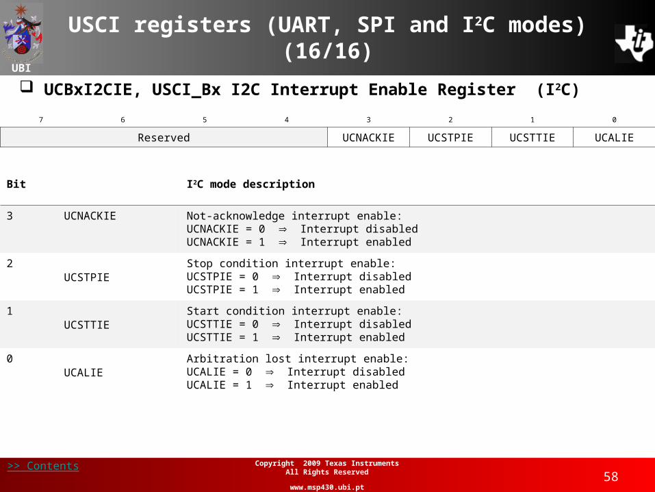
USCI registers (UART, SPI and I2C modes) (16/16)
UCBxI2CIE, USCI_Bx I2C Interrupt Enable Register (I2C)
7 6 5 4 3 2 1 0
Reserved UCNACKIE UCSTPIE UCSTTIE UCALIE
Bit I2C mode description
3 UCNACKIE Not-acknowledge interrupt enable:UCNACKIE = 0 Interrupt disabledUCNACKIE = 1 Interrupt enabled
2UCSTPIE
Stop condition interrupt enable:UCSTPIE = 0 Interrupt disabledUCSTPIE = 1 Interrupt enabled
1UCSTTIE
Start condition interrupt enable:UCSTTIE = 0 Interrupt disabledUCSTTIE = 1 Interrupt enabled
0UCALIE
Arbitration lost interrupt enable:UCALIE = 0 Interrupt disabledUCALIE = 1 Interrupt enabled
Related Documents