Freescale Semiconductor, Inc. User’s Guide © 2014 Freescale Semiconductor, Inc. 1 TWR-KV31F120M The TWR-KV31F120M microcontroller module is designed to work in standalone mode or as part of the Freescale Tower system, a modular development platform that enables rapid prototyping and tool reuse through reconfigurable hardware. Take your design to the next level and begin constructing your Tower system today by visiting www.freescale.com/tower for additional Tower System microcontroller modules and compatible peripherals. Document Number: TWRKV31F120MUG Rev. 0, 03/2014 Contents 1. TWR-KV31F120M . . . . . . . . . . . . . . . . . 1 2. Contents . . . . . . . . . . . . . . . . . . . . . . . . . . 2 3. TWR-KV31F120M features . . . . . . . . . . . 3 4. Get to know the TWR-KV31F120M . . . . 3 5. Reference documents . . . . . . . . . . . . . . . . 4 6. Hardware description . . . . . . . . . . . . . . . . 4 6.1.Microcontroller . . . . . . . . . . . . . . . . . . 5 6.2.Clocking . . . . . . . . . . . . . . . . . . . . . . . 6 6.3.System power . . . . . . . . . . . . . . . . . . . 6 6.4.Debug interface . . . . . . . . . . . . . . . . . 6 6.5.Accelerometer plus Magnetometer . . 7 6.6.Potentiometer, pushbuttons, and LEDs 8 6.7.General Purpose Tower Plug-in (TWRPI) socket 8 7. TWR-KV31F120M jumper options and headers 9 8. Useful links . . . . . . . . . . . . . . . . . . . . . . . 11 9. Revision history . . . . . . . . . . . . . . . . . . . 12 TWR-KV31F120M Tower Module User’s Guide

Welcome message from author
This document is posted to help you gain knowledge. Please leave a comment to let me know what you think about it! Share it to your friends and learn new things together.
Transcript

Freescale Semiconductor, Inc.User’s Guide
© 2014 Freescale Semiconductor, Inc.
1 TWR-KV31F120MThe TWR-KV31F120M microcontroller module is designed to work in standalone mode or as part of the Freescale Tower system, a modular development platform that enables rapid prototyping and tool reuse through reconfigurable hardware. Take your design to the next level and begin constructing your Tower system today by visiting www.freescale.com/tower for additional Tower System microcontroller modules and compatible peripherals.
Document Number: TWRKV31F120MUGRev. 0, 03/2014
Contents1. TWR-KV31F120M . . . . . . . . . . . . . . . . . 12. Contents . . . . . . . . . . . . . . . . . . . . . . . . . . 23. TWR-KV31F120M features . . . . . . . . . . . 34. Get to know the TWR-KV31F120M . . . . 35. Reference documents . . . . . . . . . . . . . . . . 46. Hardware description . . . . . . . . . . . . . . . . 4
6.1.Microcontroller . . . . . . . . . . . . . . . . . . 56.2.Clocking . . . . . . . . . . . . . . . . . . . . . . . 66.3.System power . . . . . . . . . . . . . . . . . . . 66.4.Debug interface . . . . . . . . . . . . . . . . . 66.5.Accelerometer plus Magnetometer . . 76.6.Potentiometer, pushbuttons, and LEDs 86.7.General Purpose Tower Plug-in (TWRPI) socket 8
7. TWR-KV31F120M jumper options and headers 98. Useful links . . . . . . . . . . . . . . . . . . . . . . . 119. Revision history . . . . . . . . . . . . . . . . . . . 12
TWR-KV31F120M Tower Module User’s Guide
TWR-KV31F120M Tower Module, User’s Guide, Rev. 0, 03/2014
2 Freescale Semiconductor Inc.
Contents
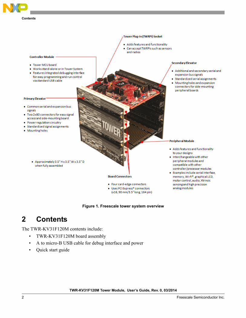
Figure 1. Freescale tower system overview
2 ContentsThe TWR-KV31F120M contents include:
• TWR-KV31F120M board assembly
• A to micro-B USB cable for debug interface and power
• Quick start guide

TWR-KV31F120M Tower Module, User’s Guide, Rev. 0, 03/2014
Freescale Semiconductor Inc. 3
TWR-KV31F120M features
3 TWR-KV31F120M features• Tower-compatible microcontroller module.
• KV31F512VLL12 MCU (120 MHz, 512 KB Flash, 96 KB RAM, low power, 100 LQFP package).
• General-purpose Tower Plug-in (TWRPI) socket.
• On-board debug circuit: K20DX128VFM5 (OpenSDA) with virtual serial port.
• FXOS8700CQ: 6-Axis Digital Sensor Accelerometer + Magnetometer.
• Four (4) user-controllable LEDs plus RGB LED.
• Four (4) user pushbutton switches for GPIO interrupts.
• One (1) user pushbutton switch for MCU reset.
• Potentiometer.
4 Get to know the TWR-KV31F120M
Figure 2. Front side of TWR-KV31F120M module (TWRPI devices not shown)

TWR-KV31F120M Tower Module, User’s Guide, Rev. 0, 03/2014
4 Freescale Semiconductor Inc.
Reference documents
5 Reference documentsThe documents listed below should be referenced for more information on the Kinetis K Series, Tower System, and MCU modules. These can be found in the documentation section of www.freescale.com/kinetis.
• TWR-KV31F120M-SCH (schematics)
• KV31P100M120SF7RM (reference manual)
• Tower configuration tool
• Tower mechanical drawing
6 Hardware descriptionThe TWR-KV31F120M is a Tower MCU Module featuring the KV31F512VLL12—a Kinetis V Series microcontroller in a 100 LQFP package with high speed run mode. It is intended for use in the Freescale Tower System but can also operate alone. An on-board OpenSDA debug circuit provides a Serial Wire Debug (SWD) interface and a power supply input through a single micro-USB connector.
The block diagram of the TWR-KV31F120M board is presented in the following figure:
Figure 3. Block Diagram of TWR-KV31F120M

TWR-KV31F120M Tower Module, User’s Guide, Rev. 0, 03/2014
Freescale Semiconductor Inc. 5
Hardware description
6.1 Microcontroller
The TWR-KV31F120M features the KV31F512VLL12 MCU. This 120 MHz microcontroller is part of the Kinetis KV3x family and is implemented in a 100 LQFP package. The following table notes some of the features of the KV31F512VLL12 MCU.
Table 1. Features of KV31F512VLL12
Feature Description
Ultra low-power
• 11 low-power modes with power and clock gating for optimal peripheral activity and recovery times.
• Full memory and analog operation down to 1.71 V for extended battery life • Low-leakage wake-up unit with up to three internal modules and 8 pins as wake-up sources
in low-leakage stop (LLS) and very low-leakage stop (VLLS) modes • Low-power timer for continual system operation in reduced power states
Flash and SRAM
• 512-KB flash featuring fast access times, high reliability, and four levels of security protection • 96 KB of SRAM • No user or system intervention to complete programming and erase functions, and full
operation down to 1.71 V
Mixed-signal capability
• High-speed 16-bit ADC with configurable resolution • Single or differential output modes for improved noise rejection • 500-ns conversion time achievable with programmable delay block triggering • Two high-speed comparators providing fast and accurate motor over-current protection by
driving PWMs to a safe state • Optional analog voltage reference provides an accurate reference to analog blocks and
replaces external voltage references to reduce system cost
Performance
• 120-MHz ARM Cortex-M4F core with DSP and FPU instruction set, single cycle MAC, and single instruction multiple data (SIMD) extensions
• Up to 16 channel DMA for peripheral and memory servicing with reduced CPU loading and faster system throughput
• Crossbar switch enables concurrent multi-master bus accesses, increasing bus bandwidth
Timing and control
• Up to four FlexTimers (FTM) with a total of 20 channels • Hardware dead-time insertion and quadrature decoding for motor control • Four-channel 32-bit periodic interrupt timer (PIT) provides time base for RTOS task
scheduler, or trigger source for ADC conversion and programmable delay block
Connectivity and communications
• Four UARTs:– one UART that supports RS232 with flow control, RS485, and ISO7816– two UARTs that support RS232 with flow control and RS485– one low power UART (LPUART)
• Two DSPI modules and two I2C modules
Reliability, safety, and security
• Cyclic redundancy check (CRC) engine validates memory contents and communication data, increasing system reliability
• Independently-clocked COP guards against clock skew or code runaway for fail-safe applications such as the IEC 60730 safety standard for household appliances
• External watchdog monitor drives output pin to safe state for external components in the event that a watchdog timeout occurs
• Included in Freescale’s product longevity program, with assured supply for a minimum of 10 years after launch

TWR-KV31F120M Tower Module, User’s Guide, Rev. 0, 03/2014
6 Freescale Semiconductor Inc.
Hardware description
6.2 Clocking
Kinetis V Series MCUs start up from an internal digitally controlled oscillator (DCO). Software can enable the main external oscillator (EXTAL0/XTAL0) if desired. The external oscillator/resonator can range from 32.768 KHz up to 32 MHz. An 8-MHz crystal is the default external source for the MCG oscillator inputs (XTAL/EXTAL).
By connecting J25 (2-3) jumper enables other external clock sources for the KV31F512VLL12 include the CLKIN0 signal, which can be provided through the TWR-ELEV module or pin 20 of TWRPI connector J6.
6.3 System power
When installed into a Tower System, the TWR-KV31F120M can be powered from either an on-board source or from another source in the assembled Tower System.
In stand-alone operation, the main power source (5.0 V) for the TWR-KV31F120M module is derived from the OpenSDA USB micro-B connector (J21). Two low-dropout regulators provide 3.3 V and 1.8 V supplies from the 5.0 V input voltage. All of the user-selectable options can be configured using two headers, J1 and J5. Refer to sheet 4 of the TWR-KV31F120M schematics for more details.
6.4 Debug interface
There are two debug interface options provided: the on-board OpenSDA circuit and an external ARM Cortex JTAG connector. The ARM Cortex JTAG connector (J19) is a standard 2x10-pin connector that provides an external debugger cable access to the JTAG interface of the KV31F512VLL12. Alternatively, the on-board OpenSDA debug interface can be used to access the debug interface of the KV31F512VLL12.
6.4.1 OpenSDA
An on-board K20DX128VFM5-based OpenSDA circuit provides a SWD debug interface to the KV31F512VLL12. A standard USB A male to micro-B male cable (provided) can be used for debugging via the USB connector (J21).
The OpenSDA interface also provides a USB to serial bridge. Drivers for the OpenSDA interface are provided in the P&E Micro OpenSDA Tower Toolkit. These drivers and more utilities can be found online at http://www.pemicro.com/opensda.

TWR-KV31F120M Tower Module, User’s Guide, Rev. 0, 03/2014
Freescale Semiconductor Inc. 7
Hardware description
6.4.2 Cortex debug connector
The Cortex Debug connector is a 20-pin (0.05") connector providing access to the SWD, JTAG, cJTAG, and EzPort signals available on the KV31 device. The pinout and KV31 pin connections to the debug connector (J19) are shown in Table 2.
Table 2. Cortex debug connector
6.5 Accelerometer plus Magnetometer
An FXOS8700CQ 6-Axis Digital Sensor Accelerometer + Magnetometer is connected to the KV31F512VLL12 MCU through an I2C interface (I2C0) and GPIO/IRQ signals (PTD0 and PTE24).
Pin Function TWR-KV31F120M connection
1 VTref 3.3 V MCU supply (MCU_PWR)
2 TMS / SWDIO PTA3/UART0_RTS_b/FTM0_CH0/JTAG_TMS/SWD_DIO
3 GND GND
4 TCK / SWCLK PTA0/UART0_CTS_b/FTM0_CH5/JTAG_CLK/SWD_CLK/EZP_CLK
5 GND GND
6 TDO/SWO PTA2/UART0_TX/FTM0_CH7/JTAG_TDO/TRACE_SWO/EZP_DO
7 Key –
8 TDI PTA1/UART0_RX/FTM0_CH6/JTAG_TDI/EZP_DI
9 GNDDetect PTA4/FTM0_CH1/MS/NMI_b/EZP_CS_b
10 nRESET RESET_b
11 Target Power 5 V supply (via jumper J20)
12 – NC
13 Target Power 5 V supply (via jumper J20)
14 – NC
15 GND GND
16 – NC
17 GND GND
18 – NC
19 GND GND
20 – NC

TWR-KV31F120M Tower Module, User’s Guide, Rev. 0, 03/2014
8 Freescale Semiconductor Inc.
Hardware description
6.6 Potentiometer, pushbuttons, and LEDs
The TWR-KV31F120M also features:
• A potentiometer connected to an ADC input signal (ADC0_SE23).
• Four pushbutton switches
• SW1-PTC6/LLWU_P10, SW2-PTC11/LLWU_P11, SW3-PTA4/LLWU_P3, SW4-PTE25.
• Four user-controllable LEDs connected to GPIO signals (optionally isolated using jumpers):
— Yellow LED (D3) to PTE1
— Red LED (D4) to PTE0
— Orange LED (D6) to PTB19
— Green LED (D7) to PTD7
• RGB LED
6.7 General Purpose Tower Plug-in (TWRPI) socket
The TWR-KV31F120M features a socket (J6 and J7) that can accept a variety of different Tower Plug-in modules featuring sensors, RF transceivers, and other peripherals. The General Purpose TWRPI socket provides access to I2C, SPI, IRQs, GPIOs, timers, analog conversion signals, TWRPI ID signals, reset, and voltage supplies. The pinout for the TWRPI Socket is defined in Table 3.
Table 3. General purpose TWRPI socket pinout
J6 J5
Pin Description Pin Description
1 5 V VCC 1 GND
2 3.3 V VCC 2 GND
3 GND 3 I2C: SCL
4 3.3 V VDDA 4 I2C: SDA
5 VSS (Analog GND) 5 GND
6 VSS (Analog GND) 6 GND
7 VSS (Analog GND) 7 GND
8 ADC: Analog 0 8 GND
9 ADC: Analog 1 9 SPI:MISO
10 VSS (Analog GND) 10 SPI:MOSI
11 VSS (Analog GND) 11 SPI:SS

TWR-KV31F120M Tower Module, User’s Guide, Rev. 0, 03/2014
Freescale Semiconductor Inc. 9
TWR-KV31F120M jumper options and headers
7 TWR-KV31F120M jumper options and headersThe following is a list of all of the jumper options on the TWR-KV31F120M. The default installed jumper settings are indicated by white text on a black background
Table 4. TWR-KV31F120M jumper options
12 ADC: Analog 2 12 SPI:CLK
13 VSS (Analog GND) 13 GND
14 VSS (Analog GND) 14 GND
15 GND 15 GPIO:GPIO0/IRQ
16 GND 16 GPIO:GPIO1/IRQ
17 ADC: TWRPI ID 0 17 UART:UART_RX or GPIO: GPIO2
18 ADC: TWRPI ID 1 18 UART:UART_TX or GPIO: GPIO3
19 GND 19 UART:UART_CTS or GPIO:GPIO4/Timer
20 Resist 20 UART:UART_CTS or GPIO:GPIO5/Timer
Option Jumper Setting Description
Clock Input Source Selection J25
1-2 Connect main EXTAL to on-board 8 MHz crystal
2-3Connect EXTAL to CLKIN0 signal on Primary Elevator (B24)
Debug Target Power J20ON Connect P5V_SDA to target power
OFF Disconnect P5V_SDA from target power
Tower Voltage Regulator Input Selector
J1
1-2[Default] Connect P5V_TRG_SDA (5V from OpenSDA) or P5_Elev to VREG_IN
2-3[EXT]Connect USB0_VBUS from Primary Elevator (A57) to VREG_IN
Board Power Selector J5
1-3Connect on-board 3.3V regulator output (P3V3_REG) to main board power line (V_BRD)
3-5Connect on-board 1.8V regulator output (P1V8) to main board power line (V_BRD)
MCU VDD current measurement J13ON Connect V_BRD to MCU_PWR
OFF Allow current measurement on MCU VDD
J6 J5
Pin Description Pin Description

TWR-KV31F120M Tower Module, User’s Guide, Rev. 0, 03/2014
10 Freescale Semiconductor Inc.
TWR-KV31F120M jumper options and headers
VDDA and VREFH Power J14ON Connect V_BRD to VDDA and VREFH
OFF Disconnect V_BRD from VDDA and VREF
LED Connections J17
1-2 Connect PTE1 to Yellow LED D3
3-4 Connect PTE0 to Red LED D4
5-6 Connect PTB19 to Orange LED D6
7-8 Connect PTD7 Green LED D7
TWRPI Current Measurement J15ON Connect V_BRD to TWRPI 3-V power (GPT_VBRD)
OFF Disconnect V_BRD from TWRPI 3-V power (GPT_VBRD)
Accelerometer/Magnetometer* I2C SCL Connection
J9ON Connect PTD2 to I2C_SCL_SNSR
OFF Disconnect PTD2 from I2C_SCL_SNSR
Accelerometer/Magnetometer I2C SDA Connection
J12ON Connect PTD3 to I2C_SDA_SNSR
OFF Disconnect PTD3 from I2C_SDA_SNSR
Accelerometer/Magnetometer I2C Slave Address
J4ON Pull accelerometer/magnetometer SA0 low
OFF Pull accelerometer/magnetometer SA0 high
Magnetometer I2C Slave Address J8
ON Pull magnetometer SA1 high
OFFPull magnetometer SA1 low (also used for accelerometer GND)
Accelerometer/Magnetometer I2C Interrupt 1
J11ON Connect PTD0 to INT1
OFF Disconnect PTD0 from INT1
Accelerometer/Magnetometer I2C Interrupt 2
J10ON Connect PTE24 to INT2
OFF Disconnect PTE24 from INT2
Potentiometer Enable J3ON Connect DAC0_OUT/ADC0_SE23 to POT_5K
OFF Disconnect DAC0_OUT/ADC0_SE23 from POT_5K
Reset Pushbutton J26
1-2 Connect SW5 to SDA_RST_TGTMCU_J_B
2-3Connect SW5 to RST_TGTMCU_B (Needed when OpenSDA is not powered)
UART RX Selection J22
1-2Connect UART0_RX_TGTMCU to UART1_RX_ELEV_BUF (Tower Elevator)
2-3Connect UART0_RX_TGTMCU to UART1_RX_TGTMCU_BUF (OpenSDA)
UART TX Selection J23
1-2Connect UART0_TX_TGTMCU to UART1_TX_ELEV_BUF (Tower Elevator)
2-3Connect UART0_TX_TGTMCU to UART1_TX_TGTMCU_BUF (OpenSDA)
Option Jumper Setting Description
TWR-KV31F120M Tower Module, User’s Guide, Rev. 0, 03/2014
Freescale Semiconductor Inc. 11
Useful links
*FXOS87000CQ Accelerometer/Magnetometer is standard. MMA8451Q Accelerometer is optional
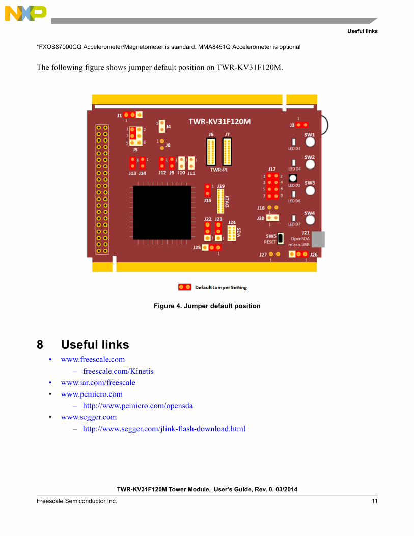
The following figure shows jumper default position on TWR-KV31F120M.
Figure 4. Jumper default position
8 Useful links• www.freescale.com
– freescale.com/Kinetis
• www.iar.com/freescale
• www.pemicro.com
– http://www.pemicro.com/opensda
• www.segger.com
– http://www.segger.com/jlink-flash-download.html

TWR-KV31F120M Tower Module, User’s Guide, Rev. 0, 03/2014
12 Freescale Semiconductor Inc.
Revision history
9 Revision historyTable 5. Revision history
Revision number Date Substantial changes
0 03/2014 Initial release

Document Number: TWRKV31F120MUGRev. 003/2014
Information in this document is provided solely to enable system and software
implementers to use Freescale products. There are no express or implied copyright
licenses granted hereunder to design or fabricate any integrated circuits based on the
information in this document.
Freescale reserves the right to make changes without further notice to any products
herein. Freescale makes no warranty, representation, or guarantee regarding the
suitability of its products for any particular purpose, nor does Freescale assume any
liability arising out of the application or use of any product or circuit, and specifically
disclaims any and all liability, including without limitation consequential or incidental
damages. “Typical” parameters that may be provided in Freescale data sheets and/or
specifications can and do vary in different applications, and actual performance may
vary over time. All operating parameters, including “typicals,” must be validated for
each customer application by customer’s technical experts. Freescale does not convey
any license under its patent rights nor the rights of others. Freescale sells products
pursuant to standard terms and conditions of sale, which can be found at the following
address: freescale.com/SalesTermsandConditions.
How to Reach Us:
Home Page: freescale.com
Web Support: freescale.com/support
Freescale, the Freescale logo, and Kinetis are trademarks of Freescale
Semiconductor, Inc., Reg. U.S. Pat. & Tm. Off. Tower is a trademark of Freescale
Semiconductor, Inc. All other product or service names are the property of their
respective owners. ARM and Cortex are registered trademarks of ARM Limited (or its
subsidiaries) in the EU and/or elsewhere. All rights reserved.
© 2014 Freescale Semiconductor, Inc.
Related Documents