Published in IET Power Electronics Received on 15th November 2012 Revised on 8th February 2013 Accepted on 22nd June 2013 doi: 10.1049/iet-pel.2012.0666 ISSN 1755-4535 Two-stage micro-grid inverter with high-voltage gain for photovoltaic applications Mahrous El-Sayed Ahmed, Mohamed Orabi, Omar Mohamed AbdelRahim Electrical Engineering Department, APEARC, Aswan Faculty of Engineering, Aswan University, Aswan 81542, Egypt E-mail: [email protected] Abstract: This study proposes a new two-stage high voltage gain boost grid-connected inverter for AC-module photovoltaic (PV) system. The proposed system consists of a high-voltage gain switched inductor boost inverter cascaded with a current shaping (CS) circuit followed by an H-bridge inverter as a folded circuit and its switches operate at line frequency. The switched inductor boost converter (SIBC) has one switch operates like a continuous conduction mode. The maximum power of the PV module is achieved through the SIBC circuit whereas the grid connection requirements are accomplished using the CS circuit with the H-bridge inverter. The switch of the CS circuit is controlled with a sine wave modulation control scheme. The main advantages of the new proposed system are high boosting gain, lower switching losses and reduces the ground leakage current as all H-bridge switches operate at the line frequency. A 120 W prototype has been built and experimentally tested. It has been found that experimental results have a good matching with the proposed analysis and simulation results. 1 Introduction The use of photovoltaic (PV) modules as a source of renewable energy is gaining attention nowadays. PV modules may be operated as an isolated system (standalone) or grid connected. PV inverters may be classified as single-stage or two-stage. The typical PV converter is based on a two-stage converter [1–7]. Two-stage configuration is mainly used because of its advantages of easy control since maximum power point tracking (MMPT) control and current injection control are decoupled at different stages. In addition, this gives the freedom to push the switching frequency of the DC–DC converter to an order higher than the inverter (the second stage) one. As a result, the size and the cost of the converter are decreased. Normally, the first stage is a DC–DC boost type converter responsible for both extracting the maximum power from the panel and boosting the PV voltage to a value higher than the peak of the grid voltage. The second stage is a DC–AC inverter that generates a sinusoidal current complied with the international standards to be either injected into the grid or to feed local and remote loads. Normally the DC voltage generated from a single PV module is a few tenths of voltage. This small DC value is not suitable to be used alone to generate the required AC voltage in standalone or in grid connection applications. These applications need peak AC voltage about 311 V (in European system). Moreover, higher modulation index (MI) can make the second stage of the DC–AC system operates in the saturation region generating higher harmonics. There are two main solutions to overcome this challenge: 1. Increasing the DC voltage value by cascading many PV modules or cascading the DC–DC converter outputs of each module [8]; 2. Increasing the DC–AC conversion gain ratio by increasing the DC–DC conversion gain ratio [9, 10]. The first aforementioned solution of cascading PV modules is not preferred because of its practical limitation and technology dependence. As a practical side, the environmental conditions especially shadow has a severe effect on the performance of the PV string system configuration. String configuration is very sensitive for environmental conditions such as shading phenomenon [11, 12]. If any partial shaded strikes any part of any module, the system will react and disconnect the whole chain, however some modules can run if they work independently. Thus the system generates a lower power than expected. Cascading the output of the DC–DC converters will solve this environmental problem, but this requires central inverter which decreases the system reliability because of failure issues. Moreover, this solution does not work with residential solution of small number of PV panels. Several topologies have been surveyed and presented to explain the second aforementioned solution. The direct solution is to utilise a transformer with high boosting ratio [10]. In this system, the 24 V DC input can be boosted to 200 V with 8.33 DC–DC conversion gain ratio and efficiency reaches approximately to 92.5%. On the other side, surveys of commercial PV inverter topologies in terms of maximum efficiency, weight and volume are presented in [1–7]. These surveys show that transformer-less topologies are more efficient, lighter, less bulky and less costly than the utilised transformer topologies. However, transformer-less topologies should pay attention into the grounding and the leakage ground currents through the PV parasitic capacitance [10]. www.ietdl.org IET Power Electron., pp. 1–10 doi: 10.1049/iet-pel.2012.0666 1 & The Institution of Engineering and Technology 2013

Welcome message from author
This document is posted to help you gain knowledge. Please leave a comment to let me know what you think about it! Share it to your friends and learn new things together.
Transcript
www.ietdl.org
IE
d
Published in IET Power ElectronicsReceived on 15th November 2012Revised on 8th February 2013Accepted on 22nd June 2013doi: 10.1049/iet-pel.2012.0666
T Power Electron., pp. 1–10oi: 10.1049/iet-pel.2012.0666
ISSN 1755-4535
Two-stage micro-grid inverter with high-voltagegain for photovoltaic applicationsMahrous El-Sayed Ahmed, Mohamed Orabi, Omar Mohamed AbdelRahim
Electrical Engineering Department, APEARC, Aswan Faculty of Engineering, Aswan University, Aswan 81542, Egypt
E-mail: [email protected]
Abstract: This study proposes a new two-stage high voltage gain boost grid-connected inverter for AC-module photovoltaic (PV)system. The proposed system consists of a high-voltage gain switched inductor boost inverter cascaded with a current shaping(CS) circuit followed by an H-bridge inverter as a folded circuit and its switches operate at line frequency. The switchedinductor boost converter (SIBC) has one switch operates like a continuous conduction mode. The maximum power of the PVmodule is achieved through the SIBC circuit whereas the grid connection requirements are accomplished using the CS circuitwith the H-bridge inverter. The switch of the CS circuit is controlled with a sine wave modulation control scheme. The mainadvantages of the new proposed system are high boosting gain, lower switching losses and reduces the ground leakagecurrent as all H-bridge switches operate at the line frequency. A 120 W prototype has been built and experimentally tested. Ithas been found that experimental results have a good matching with the proposed analysis and simulation results.
1 Introduction
The use of photovoltaic (PV) modules as a source of renewableenergy is gaining attention nowadays. PV modules may beoperated as an isolated system (standalone) or grid connected.PV inverters may be classified as single-stage or two-stage.The typical PV converter is based on a two-stage converter[1–7]. Two-stage configuration is mainly used because of itsadvantages of easy control since maximum power pointtracking (MMPT) control and current injection control aredecoupled at different stages. In addition, this gives thefreedom to push the switching frequency of the DC–DCconverter to an order higher than the inverter (the secondstage) one. As a result, the size and the cost of the converterare decreased. Normally, the first stage is a DC–DC boosttype converter responsible for both extracting the maximumpower from the panel and boosting the PV voltage to a valuehigher than the peak of the grid voltage. The second stage isa DC–AC inverter that generates a sinusoidal currentcomplied with the international standards to be either injectedinto the grid or to feed local and remote loads.Normally the DC voltage generated from a single PV
module is a few tenths of voltage. This small DC value isnot suitable to be used alone to generate the required ACvoltage in standalone or in grid connection applications.These applications need peak AC voltage about 311 V (inEuropean system). Moreover, higher modulation index (MI)can make the second stage of the DC–AC system operatesin the saturation region generating higher harmonics. Thereare two main solutions to overcome this challenge:
1. Increasing the DC voltage value by cascading many PVmodules or cascading the DC–DC converter outputs of eachmodule [8];
2. Increasing the DC–AC conversion gain ratio by increasingthe DC–DC conversion gain ratio [9, 10].
The first aforementioned solution of cascading PVmodules is not preferred because of its practical limitationand technology dependence. As a practical side, theenvironmental conditions especially shadow has a severeeffect on the performance of the PV string systemconfiguration. String configuration is very sensitive forenvironmental conditions such as shading phenomenon[11, 12]. If any partial shaded strikes any part of anymodule, the system will react and disconnect the wholechain, however some modules can run if they workindependently. Thus the system generates a lower powerthan expected. Cascading the output of the DC–DCconverters will solve this environmental problem, but thisrequires central inverter which decreases the systemreliability because of failure issues. Moreover, this solutiondoes not work with residential solution of small number ofPV panels.Several topologies have been surveyed and presented to
explain the second aforementioned solution. The directsolution is to utilise a transformer with high boosting ratio[10]. In this system, the 24 V DC input can be boosted to200 V with 8.33 DC–DC conversion gain ratio andefficiency reaches approximately to 92.5%. On the otherside, surveys of commercial PV inverter topologies in termsof maximum efficiency, weight and volume are presented in[1–7]. These surveys show that transformer-less topologiesare more efficient, lighter, less bulky and less costly thanthe utilised transformer topologies. However,transformer-less topologies should pay attention into thegrounding and the leakage ground currents through the PVparasitic capacitance [10].
1& The Institution of Engineering and Technology 2013
www.ietdl.org
Based on that, transformer-less two-stage micro-invertersare a good choice for PV grid connected applications. Bylooking to literatures, different module integrated inverters(micro-grid inverters) for PV applications are introduced[1, 6, 7, 9, 10]. In these techniques, a DC–AC converter withhigh voltage gain is attached at each module. They have aboost DC–DC converter for every PV module to save itsgenerated power by tracking its maximum power point(MPPT). Then a second stage inverter is cascaded with theDC–DC converter for grid connection requirements. Severaltopologies have been proposed in literatures to introducehigh boosting voltage gain solutions [13–20]. The highestvoltage gain reported is five times the input PV voltagethrough integrating boost converter and full bridge inverter[14]. However, this solution suffers from zero crossingcurrent distortion in addition to insufficient voltage gain. Adual boost converter circuit with only one active switch ispresented in [21]. The system achieves a simple control andhigh efficiency but its boosting ratio is approximately fivewhich is still low. Recently, multilevel boost converter ispresented as a solution for very large conversion ration [22].When higher output voltage is required, extra stages can beadded without changing the main configuration of the circuit.This circuit requires many components such as capacitor anddiodes resulting in overall system complexity, less reliability,and high cost, especially for low power PV applications.Therefore both structures, two-stage and single-stage, suffersfrom the same problem of limited boosting voltage gain.In this paper, a two-stage micro-grid inverter topology for
PV applications is proposed based on the primary ideapresented in [3]. Analysis, simulation and experimentalset-up are introduced to verify the proposed systemperformances.
2 Proposed system topology
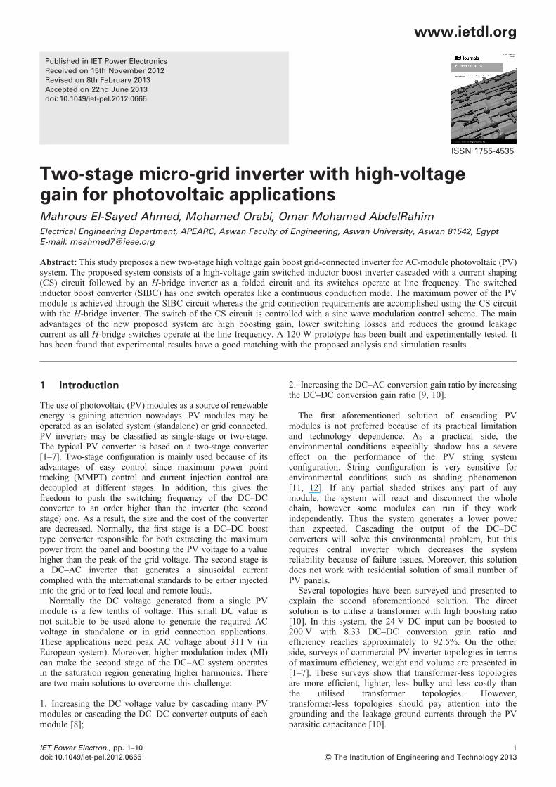
The proposed micro-inverter is shown in Fig. 1. The proposedsystem consists of SIBC cascaded with current shaping(CS)-folded cascade H-bridge. The SIBC has the advantageof high-voltage gain as the conventional DC–DC boostconverter coil is replaced with a switched inductor coil [20].The switched inductor consists of two coils and threediodes with the shown arrangement in Fig. 1. Thisarrangement enables the two coils to be charged in parallelduring the on-state and discharged in series manners duringthe off-state. The boost converter switch SW1 is designedto operate at high frequency to decrease the inductor valuesand the overall system size. The CS-folded cascadeH-bridge inverter is composed of switch SW2 and diodeD5 in addition to the bridge SW3–SW6. It has theadvantage of using only SW2 operates at the switching
Fig. 1 Schematic circuit of the proposed micro-grid inverter
2& The Institution of Engineering and Technology 2013
frequency with keeping the four switches of the H-bridgeoperate at the line frequency. This reduces the leakagecurrent and resulting in improving the proposed systemgrounding capability in addition to reducing the switchinglosses and thus the system overall efficiency can beimproved too.
3 Analysis of the proposed system
3.1 Analyses of the SIBC
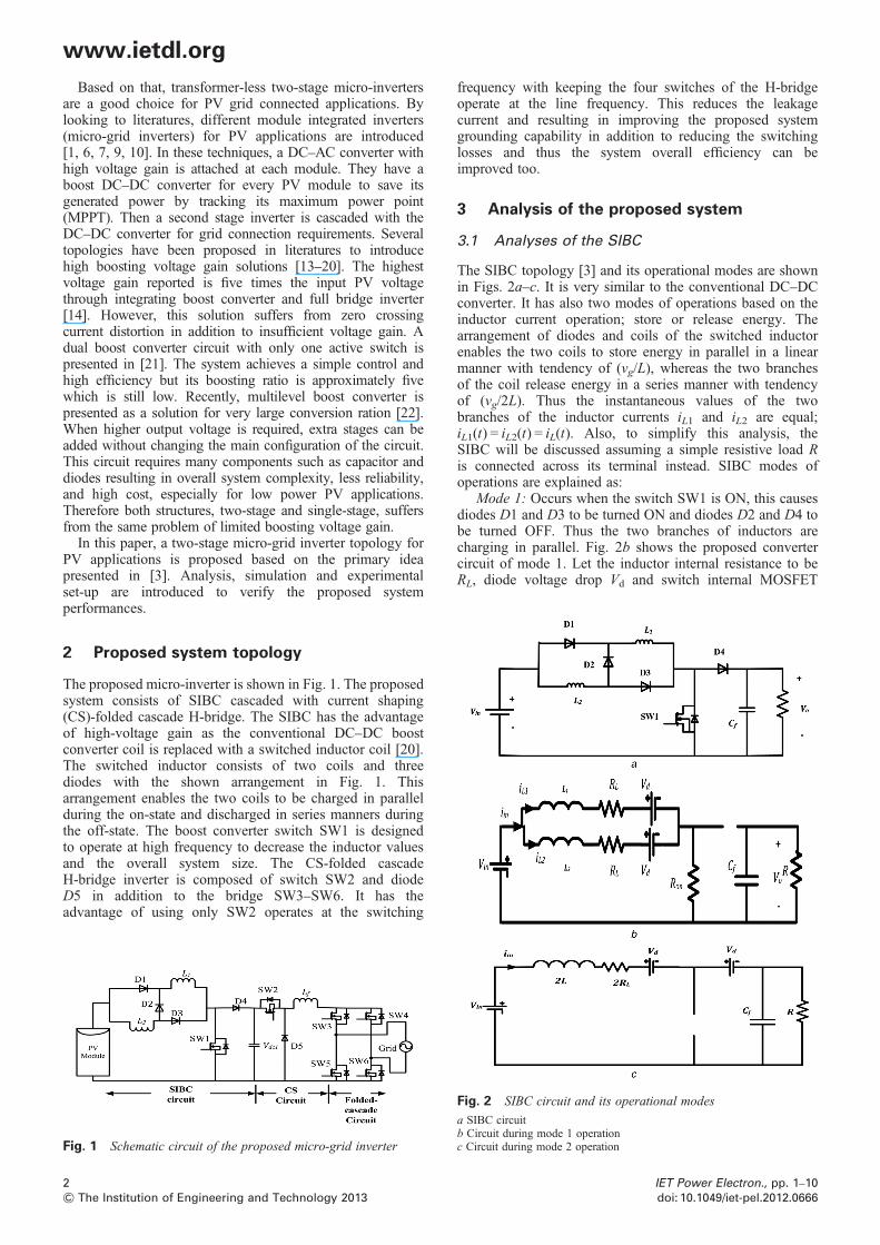
The SIBC topology [3] and its operational modes are shownin Figs. 2a–c. It is very similar to the conventional DC–DCconverter. It has also two modes of operations based on theinductor current operation; store or release energy. Thearrangement of diodes and coils of the switched inductorenables the two coils to store energy in parallel in a linearmanner with tendency of (vg/L), whereas the two branchesof the coil release energy in a series manner with tendencyof (vg/2L). Thus the instantaneous values of the twobranches of the inductor currents iL1 and iL2 are equal;iL1(t) = iL2(t) = iL(t). Also, to simplify this analysis, theSIBC will be discussed assuming a simple resistive load Ris connected across its terminal instead. SIBC modes ofoperations are explained as:
Mode 1: Occurs when the switch SW1 is ON, this causesdiodes D1 and D3 to be turned ON and diodes D2 and D4 tobe turned OFF. Thus the two branches of inductors arecharging in parallel. Fig. 2b shows the proposed convertercircuit of mode 1. Let the inductor internal resistance to beRL, diode voltage drop Vd and switch internal MOSFET
Fig. 2 SIBC circuit and its operational modes
a SIBC circuitb Circuit during mode 1 operationc Circuit during mode 2 operation
IET Power Electron., pp. 1–10doi: 10.1049/iet-pel.2012.0666
www.ietdl.org
on-resistance to be Ron. The inductor voltage vL(t), capacitorcurrent ic(t), and the input current iin(t), in this mode are givenby the following equationsvL(t) = vin(t)− 2iL(t)Ron − Vd − iLRL (1)
ic(t) = − vo(t)
R(2)
iin(t) = 2iL(t) (3)
where vin(t), vo(t) and R are the input voltage, output voltageof the SIBC and the resistor that represents the load connectedacross the SIBC, respectively.
Mode 2: Occurs when the switch SW1 is OFF, this causesdiodes D1 and D3 to be turned OFF and diodes D2 and D4 tobe turned ON and thus the two branches of the inductordischarge in series. Fig. 2c shows the proposed convertercircuit of mode 2. Similarly, the inductor voltage, thecapacitor current and the input current in this mode aregiven by the following equations
vL(t) = 0.5 vin(t)− 2Vd − 2iLRL − vo(t)( )
(4)
ic(t) = iL(t)−vo(t)
R(5)
iin(t) = 2iL(t) (6)
Then, applying inductor volt second balance and capacitorcharge balance [23], (2)–(6) yield the following equationsfor the proposed converter model
kvL(t)lT = d(t) vin(t)− 2iL(t)Ron − Vd − iLRL
[ ]+ [1− d(t)] 0.5 vin(t)− 2Vd − 2iLRL − vo(t)
( )[ ] (7)
kic(t)l = d(t) − vo(t)
R
( )+ (1− d(t)) iL(t)−
vo(t)
R
( )(8)
kiin(t)l = (i+ d(t))iL(t) (9)
From the DC analyses, the DC operating point of theproposed converter with a constant duty ratio d =D can bedetermined by equating the right-hand sides of (7) and (8)to zero and solving the two resulting algebraic equations foriL and vo, resulting in
iL = Vo
R(1− D)(10)
Vo =R(1− D) 0.5(1+ D)Vin − Vd
[ ]RL + 2RonD+ 0.5R(1− D)2
(11)
Then, the voltage boosting gain of the proposed converter isfound as
G = Vo
Vin= R(1− D) (1+ D)− 2Vd/Vin
[ ]2RL + 4RonD+ R(1− D)2
(12)
The DC component of the input current is obtained from (9)to (11) as
Lin = (1+ D)voR= (1+ D) 0.5(1+ D)Vin − Vd
[ ]RL + 2RonD+ 0.5R(1− D)2
(13)
IET Power Electron., pp. 1–10doi: 10.1049/iet-pel.2012.0666
Also, the input power of the system Pin which represents thePV extracted power PPV is derived as
Pin = PPV = Vin
(1+ D) 0.5(1+ D)Vin − Vd
[ ]RL + 2RonD+ 0.5R(1− D)2
(14)
From (10) to (14), the efficiency of the DC–DC SIBC iscalculated as follows
hSIBC = v2o/R
VinIin= G
voRIin
= G(1− D)
(1+ D)(15)
To study the performances of the SIBC, the aforementionedderived analysis has been used advantageously. The effectof the SIBC circuit parameters has been considered for theconverter boosting gain and its efficiency. The usedparameters in this test are Vin = 20 V, RL = 0.01 Ω, Ron =0.01 Ω, R = 200 Ω and Vd = 1.5 V.
Fig. 3a shows a comparison between the gain of the SIBCand conventional boost converter in ideal case. This figureshows that, the gain of the SIBC is theoretically higher thanthe conventional boost converter by a factor of (1 +D).Applying the practical conditions of the circuit parameters,Figs. 3b and c gives the gain and the efficiency of the SIBCagainst duty cycle for various values of input voltages,respectively. The first observation yields from these twocurves is that, the converter enters the unstable regionbeyond duty cycle 0.9. Therefore it should keep the dutycycle below 0.9. The effect of changing the input voltageon the gain is small because as the input voltage increasesresults in slight increase on the gain for the same duty cycleas shown in Fig. 3b. On the other hand, the effect ofchanging the input voltage on the SIBC efficiency is verynoticeably. As the input voltage decreases, it results indeterioration of the converter efficiency as shown inFig. 3c. It can be concluded that, the used input voltage forthis technique should not be less than 20 V to obtain anacceptable efficiency.
Figs. 3d and e illustrate the gain and the efficiency of theSIBC against duty cycle for various values of switchon-resistance, respectively. Figs. 3d and e reveal that, theeffect of the switch on-resistance on both the converter gainand also the efficiency is very trivial especially for lowvalues of duty cycle (below 0.6). However, the converterefficiency starts to deteriorate as the duty cycle becomescloser to 0.8. Therefore it limits the upper limit for the dutycycle operation.The calculated efficiency of (14) has been plotted against
the output power for various values of input voltage asshown in Fig. 3f. The main observation is that, as the inputvoltage increases, the converter efficiency is improved forthe same output power. It is worth to note that for inputvoltage less than 20 V, the converter efficiency decreasesvary rapidly lower than 90% which means the converter iseconomically failed.
3.2 Analyses of the CS-cascaded H-bridge circuit
The CS-cascaded H-bridge circuit composed of a CS circuitand a folded cascade H-bridge inverter. The CS circuitconsists of single controlled switch SW2, single diode D5and filter inductance Lf. The CS circuit utilises the chargingand discharging increments of boost inductor current toshape a sinusoidal rectified current [24, 25]. Then thefolded cascade H-bridge inverter reforms this rectified
3& The Institution of Engineering and Technology 2013
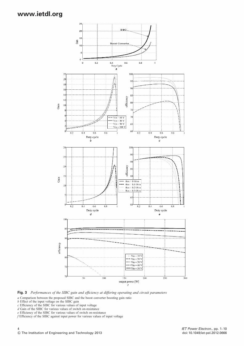
Fig. 3 Performances of the SIBC gain and efficiency at differing operating and circuit parameters
a Comparison between the proposed SIBC and the boost converter boosting gain ratiob Effect of the input voltage on the SIBC gainc Efficiency of the SIBC for various values of input voltaged Gain of the SIBC for various values of switch on-resistancee Efficiency of the SIBC for various values of switch on-resistancef Efficiency of the SIBC against input power for various values of input voltage
www.ietdl.org
4& The Institution of Engineering and Technology 2013
IET Power Electron., pp. 1–10doi: 10.1049/iet-pel.2012.0666
www.ietdl.org
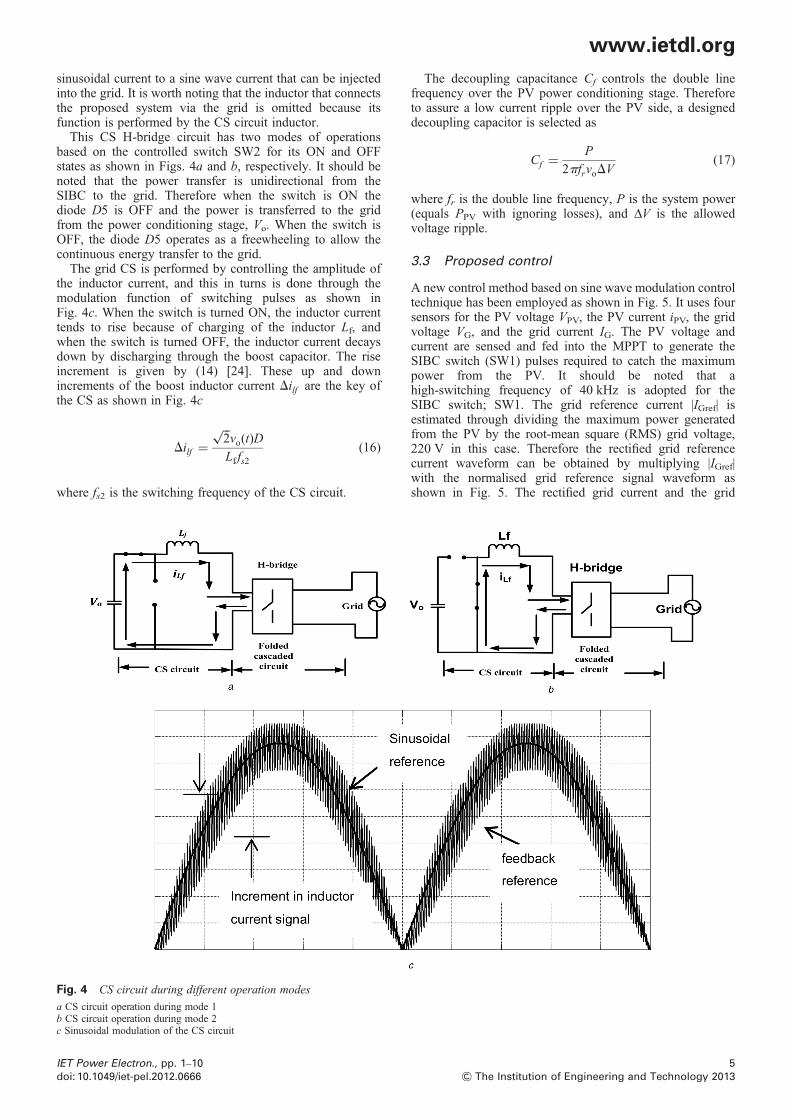
sinusoidal current to a sine wave current that can be injectedinto the grid. It is worth noting that the inductor that connectsthe proposed system via the grid is omitted because itsfunction is performed by the CS circuit inductor.This CS H-bridge circuit has two modes of operationsbased on the controlled switch SW2 for its ON and OFFstates as shown in Figs. 4a and b, respectively. It should benoted that the power transfer is unidirectional from theSIBC to the grid. Therefore when the switch is ON thediode D5 is OFF and the power is transferred to the gridfrom the power conditioning stage, Vo. When the switch isOFF, the diode D5 operates as a freewheeling to allow thecontinuous energy transfer to the grid.The grid CS is performed by controlling the amplitude of
the inductor current, and this in turns is done through themodulation function of switching pulses as shown inFig. 4c. When the switch is turned ON, the inductor currenttends to rise because of charging of the inductor Lf, andwhen the switch is turned OFF, the inductor current decaysdown by discharging through the boost capacitor. The riseincrement is given by (14) [24]. These up and downincrements of the boost inductor current Dilf are the key ofthe CS as shown in Fig. 4c
Dilf =��2
√vo(t)D
Lf fs2(16)
where fs2 is the switching frequency of the CS circuit.
Fig. 4 CS circuit during different operation modes
a CS circuit operation during mode 1b CS circuit operation during mode 2c Sinusoidal modulation of the CS circuit
IET Power Electron., pp. 1–10doi: 10.1049/iet-pel.2012.0666
The decoupling capacitance Cf controls the double linefrequency over the PV power conditioning stage. Thereforeto assure a low current ripple over the PV side, a designeddecoupling capacitor is selected as
Cf =P
2pfrvoDV(17)
where fr is the double line frequency, P is the system power(equals PPV with ignoring losses), and ΔV is the allowedvoltage ripple.
3.3 Proposed control
A new control method based on sine wave modulation controltechnique has been employed as shown in Fig. 5. It uses foursensors for the PV voltage VPV, the PV current iPV, the gridvoltage VG, and the grid current IG. The PV voltage andcurrent are sensed and fed into the MPPT to generate theSIBC switch (SW1) pulses required to catch the maximumpower from the PV. It should be noted that ahigh-switching frequency of 40 kHz is adopted for theSIBC switch; SW1. The grid reference current |IGref| isestimated through dividing the maximum power generatedfrom the PV by the root-mean square (RMS) grid voltage,220 V in this case. Therefore the rectified grid referencecurrent waveform can be obtained by multiplying |IGref|with the normalised grid reference signal waveform asshown in Fig. 5. The rectified grid current and the grid
5& The Institution of Engineering and Technology 2013
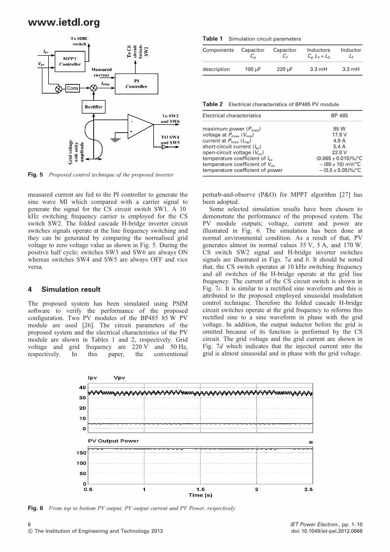
Fig. 5 Proposed control technique of the proposed inverter
Table 1 Simulation circuit parameters
Components CapacitorCp
CapacitorCf
InductorsCp L1 = L2
InductorLf
description 100 µF 220 µF 3.3 mH 3.3 mH
Table 2 Electrical characteristics of BP485 PV module
Electrical characteristics BP 485
maximum power (Pmax) 85 Wvoltage at Pmax (Vmp) 17.8 Vcurrent at Pmax (Imp) 4.9 Ashort-circuit current (Isc) 5.4 Aopen-circuit voltage (Voc) 22.0 Vtemperature coefficient of Isc (0.065 ± 0.015)%/°Ctemperature coefficient of Voc − (80 ± 10) mV/°Ctemperature coefficient of power − (0.5 ± 0.05)%/°C
www.ietdl.org
measured current are fed to the PI controller to generate thesine wave MI which compared with a carrier signal togenerate the signal for the CS circuit switch SW1. A 10kHz switching frequency carrier is employed for the CSswitch SW2. The folded cascade H-bridge inverter circuitswitches signals operate at the line frequency switching andthey can be generated by comparing the normalised gridvoltage to zero voltage value as shown in Fig. 5. During thepositive half cycle; switches SW3 and SW6 are always ONwhereas switches SW4 and SW5 are always OFF and viceversa.
4 Simulation result
The proposed system has been simulated using PSIMsoftware to verify the performance of the proposedconfiguration. Two PV modules of the BP485 85 W PVmodule are used [26]. The circuit parameters of theproposed system and the electrical characteristics of the PVmodule are shown in Tables 1 and 2, respectively. Gridvoltage and grid frequency are 220 V and 50 Hz,respectively. In this paper, the conventional
Fig. 6 From top to bottom PV output, PV output current and PV Powe
6& The Institution of Engineering and Technology 2013
perturb-and-observe (P&O) for MPPT algorithm [27] hasbeen adopted.Some selected simulation results have been chosen to
demonstrate the performance of the proposed system. ThePV module outputs; voltage, current and power areillustrated in Fig. 6. The simulation has been done atnormal environmental condition. As a result of that, PVgenerates almost its normal values 35 V, 5 A, and 170 W.CS switch SW2 signal and H-bridge inverter switchessignals are illustrated in Figs. 7a and b. It should be notedthat, the CS switch operates at 10 kHz switching frequencyand all switches of the H-bridge operate at the grid linefrequency. The current of the CS circuit switch is shown inFig. 7c. It is similar to a rectified sine waveform and this isattributed to the proposed employed sinusoidal modulationcontrol technique. Therefore the folded cascade H-bridgecircuit switches operate at the grid frequency to reforms thisrectified sine to a sine waveform in phase with the gridvoltage. In addition, the output inductor before the grid isomitted because of its function is performed by the CScircuit. The grid voltage and the grid current are shown inFig. 7d which indicates that the injected current into thegrid is almost sinusoidal and in phase with the grid voltage.
r, respectively
IET Power Electron., pp. 1–10doi: 10.1049/iet-pel.2012.0666
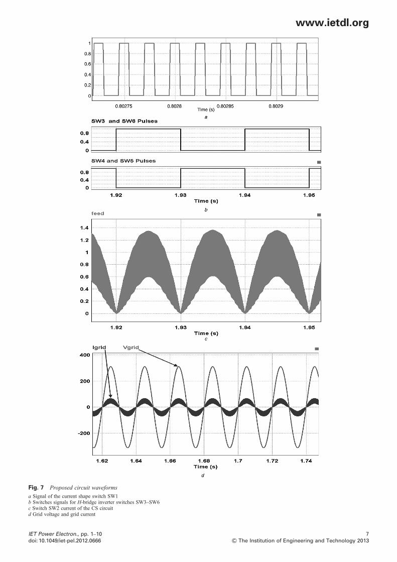
Fig. 7 Proposed circuit waveforms
a Signal of the current shape switch SW1b Switches signals for H-bridge inverter switches SW3–SW6c Switch SW2 current of the CS circuitd Grid voltage and grid current
www.ietdl.org
IET Power Electron., pp. 1–10doi: 10.1049/iet-pel.2012.0666
7& The Institution of Engineering and Technology 2013
www.ietdl.org
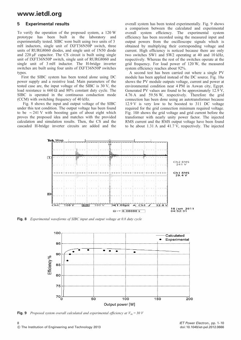
5 Experimental resultsTo verify the operation of the proposed system, a 120 Wprototype has been built in the laboratory andexperimentally tested. SIBC were built using two units of 3mH inductors, single unit of IXFT36N50P switch, threeunits of RURG8060 diodes, and single unit of 1N50 diodeand 220 µF capacitor. The CS circuit is built using singleunit of IXFT36N50P switch, single unit of RURG8060 andsingle unit of 3 mH inductor. The H-bridge inverterswitches are built using four units of IXFT36N50P switchestypes.First the SIBC system has been tested alone using DC
power supply and a resistive load. Main parameters of thetested case are, the input voltage of the SIBC is 30 V, theload resistance is 660 Ω and 80% constant duty cycle. TheSIBC is operated in the continuous conduction mode(CCM) with switching frequency of 40 kHz.
Fig. 8 shows the input and output voltage of the SIBCunder this test condition. The output voltage has been foundto be ∼ 241 V with boosting gain of about eight whichproves the proposed idea and matches with the providedcalculation and simulation results. Then, the CS and thecascaded H-bridge inverter circuits are added and the
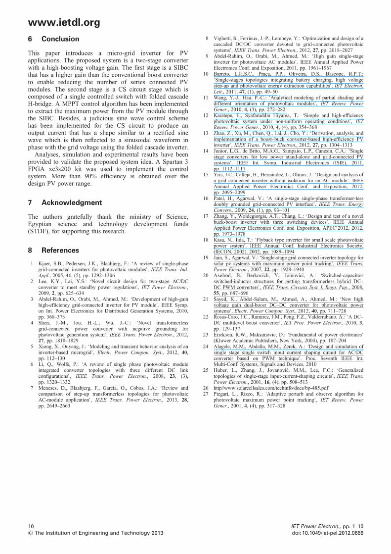
Fig. 9 Proposed system overall calculated and experimental efficiency
Fig. 8 Experimental waveforms of SIBC input and output voltage at 0.
8& The Institution of Engineering and Technology 2013
overall system has been tested experimentally. Fig. 9 showsa comparison between the calculated and experimentaloverall system efficiency. The experimental systemefficiency has been recorded using the measured input andoutput powers from the oscilloscope signals which isobtained by multiplying their corresponding voltage andcurrent. High efficiency is noticed because there are onlytwo switches SW1 and SW2 operating at 40 and 10 kHz,respectively. Whereas the rest of the switches operate at thegrid frequency. For load power of 120 W, the measuredsystem efficiency reaches about 92%.A second test has been carried out where a single PV
module has been applied instead of the DC source. Fig. 10ashows the PV module outputs voltage, current and power atenvironmental condition near 4 PM in Aswan city, Egypt.Generated PV values are found to be approximately 12.9 V,4.76 A and 59.56 W, respectively. Therefore the gridconnection has been done using an autotransformer because12.9 V is very low to be boosted to 311 DC voltagerequired for the grid connection minimum required voltage.Fig. 10b shows the grid voltage and grid current before thetransformer with nearly unity power factor. The injectedRMS current and the RMS output voltage have been foundto be about 1.31 A and 41.7 V, respectively. The injected
at Vin = 30 V
8 duty cycle
IET Power Electron., pp. 1–10doi: 10.1049/iet-pel.2012.0666
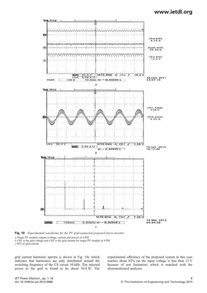
Fig. 10 Experimental waveforms for the PV grid-connected proposed micro-inverter
a Single PV module outputs (voltage, current and power) at 4 PMb CH1 is the grid voltage and CH2 is the grid current for single PV module at 4 PMc FFT of grid current
www.ietdl.org
grid current harmonic spectra is shown in Fig. 10c whichindicates that harmonics are only distributed around theswitching frequency of the CS circuit 10 kHz. The injectedpower to the grid is found to be about 54.8 W. The
IET Power Electron., pp. 1–10doi: 10.1049/iet-pel.2012.0666
experimental efficiency of the proposed system in this casereaches about 82% (as the input voltage is less than 13 Vbecause of test limitation) which is matched with theaforementioned analyses.
9& The Institution of Engineering and Technology 2013
www.ietdl.org
6 ConclusionThis paper introduces a micro-grid inverter for PVapplications. The proposed system is a two-stage converterwith a high-boosting voltage gain. The first stage is a SIBCthat has a higher gain than the conventional boost converterto enable reducing the number of series connected PVmodules. The second stage is a CS circuit stage which iscomposed of a single controlled switch with folded cascadeH-bridge. A MPPT control algorithm has been implementedto extract the maximum power from the PV module throughthe SIBC. Besides, a judicious sine wave control schemehas been implemented for the CS circuit to produce anoutput current that has a shape similar to a rectified sinewave which is then reflected to a sinusoidal waveform inphase with the grid voltage using the folded cascade inverter.Analyses, simulation and experimental results have been
provided to validate the proposed system idea. A Spartan 3FPGA xc3s200 kit was used to implement the controlsystem. More than 90% efficiency is obtained over thedesign PV power range.
7 Acknowledgment
The authors gratefully thank the ministry of Science,Egyptian science and technology development funds(STDF), for supporting this research.
8 References
1 Kjaer, S.B., Pedersen, J.K., Blaabjerg, F.: ‘A review of single-phasegrid-connected inverters for photovoltaic modules’, IEEE Trans. Ind.Appl., 2005, 41, (5), pp. 1292–1306
2 Lee, K.Y., Lai, Y.S.: ‘Novel circuit design for two-stage AC/DCconverter to meet standby power regulations’, IET Power Electron.,2009, 2, pp. 625–634
3 Abdel-Rahim, O., Orabi, M., Ahmed, M.: ‘Development of high-gainhigh-efficiency grid-connected inverter for PV module’. IEEE Symp.on Int. Power Electronics for Distributed Generation Systems, 2010,pp. 368–373
4 Shen, J.-M., Jou, H.-L., Wu, J.-C.: ‘Novel transformerlessgrid-connected power converter with negative grounding forphotovoltaic generation system’, IEEE Trans. Power Electron., 2012,27, pp. 1818–1829
5 Xiong, X., Ouyang, J.: ‘Modeling and transient behavior analysis of aninverter-based microgrid’, Electr. Power Compon. Syst., 2012, 40,pp. 112–130
6 Li, Q., Wolfs, P.: ‘A review of single phase photovoltaic moduleintegrated converter topologies with three different DC linkconfigurations’, IEEE Trans. Power Electron., 2008, 23, (3),pp. 1320–1332
7 Meneses, D., Blaabjerg, F., García, O., Cobos, J.A.: ‘Review andcomparison of step-up transformerless topologies for photovoltaicAC-module application’, IEEE Trans. Power Electron., 2013, 28,pp. 2649–2663
10& The Institution of Engineering and Technology 2013
8 Vighetti, S., Ferrieux, J.-P., Lembeye, Y.: ‘Optimization and design of acascaded DC/DC converter devoted to grid-connected photovoltaicsystems’, IEEE Trans. Power Electron., 2012, 27, pp. 2018–2027
9 Abdel-Rahim, O., Orabi, M., Ahmed, M.: ‘High gain single-stageinverter for photovoltaic AC modules’. IEEE Annual Applied PowerElectronics Conf. and Exposition, 2011, pp. 1961–1967
10 Barreto, L.H.S.C., Praça, P.P., Oliveira, D.S., Bascope, R.P.T.:‘Single-stages topologies integrating battery charging, high voltagestep-up and photovoltaic energy extraction capabilities’, IET Electron.Lett., 2011, 47, (1), pp. 49–50
11 Wang, Y.-J., Hsu, P.-C.: ‘Analytical modeling of partial shading anddifferent orientation of photovoltaic modules’, IET Renew. PowerGener., 2010, 4, (3), pp. 272–282
12 Karatepe, E., Syafaruddin Hiyama, T.: ‘Simple and high-efficiencyphotovoltaic system under non-uniform operating conditions’, IETRenew. Power Gener., 2010, 4, (4), pp. 354–368
13 Zhao, Z., Xu, M., Chen, Q., Lai, J., Cho, Y.: ‘Derivation, analysis, andimplementation of a boost–buck converter-based high-efficiency PVinverter’, IEEE Trans. Power Electron., 2012, 27, pp. 1304–1313
14 Junior, L.G., de Brito, M.A.G., Sampaio, L.P., Canesin, C.A.: ‘Singlestage converters for low power stand-alone and grid-connected PVsystems’. IEEE Int. Symp. Industrial Electronics (ISIE), 2011,pp. 1112–1117
15 Yris, J.C., Calleja, H., Hernández, L., Olmos, J.: ‘Design and analysis ofa grid connected inverter without isolation for an AC module’. IEEEAnnual Applied Power Electronics Conf. and Exposition, 2012,pp. 2095–2099
16 Patel, H., Agarwal, V.: ‘A single-stage single-phase transformer-lessdoubly grounded grid-connected PV interface’, IEEE Trans. EnergyConvers., 2009, 24, (1), pp. 93–101
17 Zhang, Y., Woldegiorgis, A.T., Chang, L.: ‘Design and test of a novelbuck-boost inverter with three switching devices’. IEEE AnnualApplied Power Electronics Conf. and Exposition, APEC’2012, 2012,pp. 1973–1978
18 Kasa, N., Iida, T.: ‘Flyback type inverter for small scale photovoltaicpower system’. IEEE Annual Conf. Industrial Electronics Society,(IECON, 2002), 2002, pp. 1089–1094
19 Jain, S., Agarwal, V.: ‘Single-stage grid connected inverter topology forsolar pv systems with maximum power point tracking’, IEEE Trans.Power Electron., 2007, 22, pp. 1928–1940
20 Axelrod, B., Berkovich, Y., Ioinovici, A.: ‘Switched-capacitor/switched-inductor structures for getting transformerless hybrid DC–DC PWM converters’, IEEE Trans. Circuits Syst. I, Regu. Pap., 2008,55, pp. 687–696
21 Sayed, K., Abdel-Salam, M., Ahmed, A., Ahmed, M.: ‘New highvoltage gain dual-boost DC–DC converter for photovoltaic powersystems’, Electr. Power Compon. Syst., 2012, 40, pp. 711–728
22 Rosas-Caro, J.C., Ramirez, J.M., Peng, F.Z., Valderrabano, A.: ‘A DC–DC multilevel boost converter’, IET Proc. Power Electron., 2010, 3,pp. 129–137
23 Erickson, R.W., Maksimovic, D.: ‘Fundamental of power electronics’(Kluwer Academic Publishers, New York, 2004), pp. 187–204
24 Alagele, M.M., Abdalla, M.M., Zerek, A.: ‘Design and simulation ofsingle stage single switch input current shaping circuit for AC/DCconverter based on PWM technique’. Proc. Seventh IEEE Int.Multi-Conf. Systems, Signals and Devices, 2010
25 Huber, L., Zhang, J., Jovanovic,́ M.M., Lee, F.C.: ‘Generalizedtopologies of single-stage input-current-shaping circuits’, IEEE Trans.Power Electron., 2001, 16, (4), pp. 508–513
26 http//www.solarcellsales.com/techinfo/docs/bp-485.pdf27 Piegari, L., Rizzo, R.: ‘Adaptive perturb and observe algorithm for
photovoltaic maximum power point tracking’, IET Renew. PowerGener., 2001, 4, (4), pp. 317–328
IET Power Electron., pp. 1–10doi: 10.1049/iet-pel.2012.0666
Related Documents