94 TWO DIMENSIONAL NUMERICAL ANALYSIS FOR DEVICES WITH FREE STEP DESIGN METHOD Koichi Sakamoto, Jun Ueda, Tatsuro Miyoshi, and Shlntaro Ushio OKI Electric Industry Company, Ltd. 550-1, Higashiasakawa, Hachioji, Tokyo 193, Japan ABSTRACT The algorithms for device simulation for arbitrary device structure and general analysis were studied, and a two dimen- sional device simulation program was developed. The program is composed of a pre-processor which functions as the user interface, and a device simulator that is independent of de- vice structure. The pre-processor translates device structure data into the input data for device simulator. The pre-pro- cessor also determines the sequence of steps according to de- vice type and purpose of analysis. In each step, solved equations, physical models, and convergence conditions are specified. Device simulation yields a numerical solution according to designed steps and gives a more accurate solu- tion while using less computation time. The depletion layer analysis sets the initial condition for numerical solution independent of the device structure and bias conditions. The avalanche effect of n-channel MOSFETs was analyzed by this program. MOSFETs with four gates and npn-bipolar transistors can be analyzed only if user input data is changed. Programs having these algorithms can effectively analyze the arbitrary device structures with any bias condition, and can satisfy any user requirements. 1. INTRODUCTION Two dimensional device simulation is useful for device design of MOS integrated circuits because the experimental investigation of device characteristics is time consuming. According to recent advances in IC process technology, the optimal design of MOS devices has been made more difficult because of their complicated structures, for example, LDD MOSFETs. Therefore device simulation programs are necessary to analyze complicated device structures.

Welcome message from author
This document is posted to help you gain knowledge. Please leave a comment to let me know what you think about it! Share it to your friends and learn new things together.
Transcript
94
TWO DIMENSIONAL NUMERICAL ANALYSIS FOR DEVICES WITH FREE STEP DESIGN METHOD
Koichi Sakamoto, Jun Ueda, Tatsuro Miyoshi, and Shlntaro Ushio
OKI Electric Industry Company, Ltd. 550-1, Higashiasakawa, Hachioji, Tokyo 193, Japan
ABSTRACT
The algorithms for device simulation for arbitrary device structure and general analysis were studied, and a two dimensional device simulation program was developed. The program is composed of a pre-processor which functions as the user interface, and a device simulator that is independent of device structure. The pre-processor translates device structure data into the input data for device simulator. The pre-processor also determines the sequence of steps according to device type and purpose of analysis. In each step, solved equations, physical models, and convergence conditions are specified. Device simulation yields a numerical solution according to designed steps and gives a more accurate solution while using less computation time. The depletion layer analysis sets the initial condition for numerical solution independent of the device structure and bias conditions. The avalanche effect of n-channel MOSFETs was analyzed by this program. MOSFETs with four gates and npn-bipolar transistors can be analyzed only if user input data is changed. Programs having these algorithms can effectively analyze the arbitrary device structures with any bias condition, and can satisfy any user requirements.
1. INTRODUCTION
Two dimensional device simulation is useful for device design of MOS integrated circuits because the experimental investigation of device characteristics is time consuming. According to recent advances in IC process technology, the optimal design of MOS devices has been made more difficult because of their complicated structures, for example, LDD MOSFETs. Therefore device simulation programs are necessary to analyze complicated device structures.

Many programs [l][2][3] developed for MOSFET solve b
Poisson's equation and one current continuity equation for electron or hole. These programs require little computation time for analysis, but they omit the physical models such as carrier generation and recombination because the models are negligible in the long channel MOS devices under the normal bias condition. Several simulation programs [it] [5] [6] solve electrostatic potential, electron concentration, and hole concentration, and these programs analyze the avalanche breakdown phenomena in MOS devices. These above mentioned programs are still used exclusively for standard device structure. Some of these programs consume much computation time to analyze the device under higher bias conditions because they use thermal equilibrium as the initial condition for the numerical solution.
This paper focuses the algorithms for device simulation programs which analyze arbitrary device structures under any bias conditions. The algorithms also analyze standard devices using computation time comparable to that of the exclusive programs. To evaluate the algorithms for the program the Universal Semiconductor Analysis System (UNISAS) was developed. In section 2, an overview of UNISAS is introduced. UNISAS is composed mainly of a pre-processor and a two dimensional device simulator with free step design method. In section 3, the algorithm of the pre-processor is discussed. In section h, the numerical and physical models used in the device simulator are explained, and a new method of setting the initial condition for numerical solution is discussed. In section 5, the simulation results and effectiveness of the program are shown and discussed.
2. OVERVIEW OF UNISAS
Conventional simulation programs can solve only standard device structures. But device designers need to analyze arbitrary device structure under any bias condition. These requirements increase the complexity of the algorithm and computation time of device simulation. The methods defining of device configuration and setting the initial condition for numerical solutions become more complicated due to dependence on device structure.
To solve these problems, a device simulation program and a new method of setting initial conditions are proposed. The program is composed of a pre-processor (PPDS) for user interaction, and a main processor (DSS) independent of the device structure. PPDS translates the input data of device configuration into detail information for numerical solution under DSS. The initial condition fer numerical solution is set by depletion layer analysis, independent of the device structure for any bias condition.

96 In DSS the solved equations and physical models are pre
pared sufficiently for analysis of any device type, and these assortments may increase computation time. We proposed a new method, called the free step design method, to execute device simulation using equations and physical models suitable for analysis. This method keeps DSS independent of device structure. DSS is executed according to the step sequence, which include solved equations, physical models and convergence conditions for numerical solutions. DSS yields better solution with less computation time under this method. Under the free step design method, PPDS find the optimal steps considering device type and purpose of analysis specified by the user.
DSS is completely independent of device structure, or purpose of analysis.
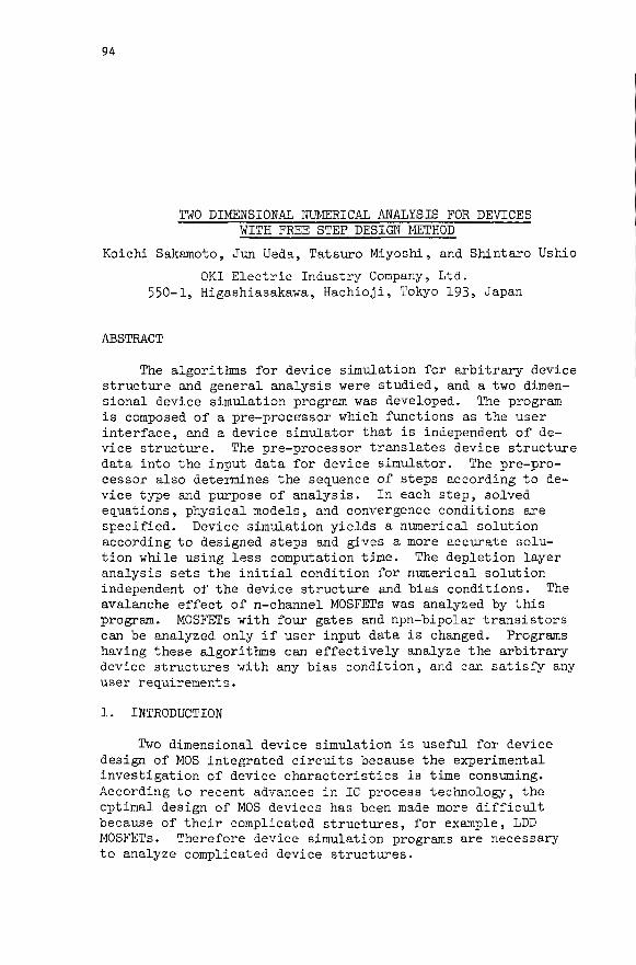
Figure 1 shows a composition of UNISAS which includes PPDS, DSS, an one dimensional process simulator (ASPREM), and graphic output program (VDIOS). Input data from users is also shown in this figure. The impurity distribution isicalcu-lated by ASPREM, which is the improved SUPREME [7] for multilayer structures consisting of silicon-oxide, silicon-nitride and poly-silicon layers. Physical models, such as oxidation-enhanced diffusion are also improved. The results of the process and device simulations are sent to VDIOS and dispicted on graphic display. VDIOS can dispict contour-plots, birds-eye-views and so on. The circuit simulator receives the parameters of the device model calculated by DSS,
3. ALGORITHM OF PPDS
PPDS translates input data of device structures and finds the optimal step design of device simulation.
To translate device-structure data given by the user into input data for DSS, PPDS defines nodes and boundaries for numerical solutions. Nodes are the intersections of grid lines divided according to input data and position of pn-junctions. Boundaries on the device-configuration edge comprise a closed loop. Each node is classified by type of material such as semiconductor or insulator, and by its position in the grid space for numerical solution, for example, in, on, or outside the closed loop. The impurity distribution is mapped on each node according to input data. Boundaries that are chains of node are classified by numerical solution, for example, they are classified as having hold or free boundaries. DSS can perform device simulation if it reads the data with respect to the nodes and boundaries made by PPDS.
PPDS will specify the optimaltsequence of steps for device simulation according to device type and purpose of analysis. For standard MOSFET devices one-carrier analysis is performed, then two-carrier analysis having an avlanche effect
i s performed in order to decrease computation t ime. For device analys is of p o t e n t i a l d i s t r i b u t i o n with low cu r r en t , one -ca r r i e r ana lys is with a higher accuracy of p o t e n t i a l i s used.
97
Input data from users is interpreted by language developed for this program. Users can define the device structures, the interfaces for ASPREM, the mapping method for two dimensional impurity distribution, physical models, convergence conditions for numerical solution, bias conditions, and the interface of VDIOS. For arbitrary device structures, users must describe detail information, for example, definition of geometrical elements which compose device configuration and definition of boundaries. For standard device structures like MOSFETs, input data fo,_ device structure is saved in a disk file, and the users can describe the input data to be changed.
Figure 2 shows an example of formats for one set bias analysis of n-channel MOSFET. These formats are simple and clear for user. Figure 3 shows the device geometry, the pn-junctionti, and nodes for numerical solutions where PPDS has translated the input data of the n-channel MOSFET in Fig. 2. The grid intervals are smallest at the pn-junctions in the horizontal direction, and .at the interface in the vertical direction, respectively, where the current densities change greatly.
PROCESS DATA
DEVICE STRUCTURE DATA
ELECTRODE VOLTAGE
V
ASPREM
CIRCUIT SIMULATOR
Fig. 1 Composition of UNISAS

98 *ODESA DEVICE = MOSFET, SUBSTRATE = P *DATA GATE.LENGTH =2.0, GATE.THICKNESS =0.03 LFT.ELE = IMP, MOB.ELE = YAMAGUCHI GNR.ELE = IMPACT LFT.HOL = IMP, MOB.HOL = YAMAGUCHI GNR.HOL = IMPACT *RUN VGS = 14.0, VDS = 7.5, VBS = 0.0 OP.A.POT = MD *END
Fig. 2 Input formats of PPDS for standard n-channe.l MOSFET
SOURCE GATE DRAIN
Ml H11H1HWH1 I N
SUBSTRATE, _ i 1
— 1.0 a.a 1.3 2.a 3.0 4.0 s.a s.a 7.0
Fig. 3 Device geometry and discretization nodes for standard n-channel MOSFET
h. PHYSICAL AND NUMERICAL MODELS IN DSS
DSS performs device simulation independent of device structures and user requirements, according to the designed steps and the informations about nodes and boundaries. To set the initial condition for the numerical solution, depletion layer analysis is used because it is independent of device structure and bias condition.
it.l Numerical models
In each step of device simulation, Poisson's equation and current continuity equation for electron and hole can be solved. The continuous forms of these equations, in semiconductor are
V-(cV*)=-q(p-n + r)-Qss 1
59 -V-y„=G-R-Rs (2)
Wp=G-R-Rs (3)
where
yn=-/LtenV^ + DnVn (k)
Jp=-yuPpVvJ'-DpVp (5)
Here, i|>, T, and Qss are electrostatic potential, impurity concentration, and charge concentration representing the fixed charge at the interface, n and p are the electron and hole concentrations, Jn and Jj> are the electron and hole current densities, G and R are the generation and recombination rates, un and yp are the electron and hole mobility, Dn and Dp are the electron and hole diffusivities, and e and q are permi-tivity and the absolute magnitude of the electron charge. Rs is the generation-recombination rate at the interface. In Eqs. (2) - (5), J n and Jj> are normalized by q. In insulator n, p, and T is zero.
In DSS Poisson's equation (l) is linearized by Gummel's algorithm[8], and expressed as
V<rV<5)-^£(p + n)<5=-V<£V*')-q(p-n+r)-Qss (6)
where 6=^'i*i—+'
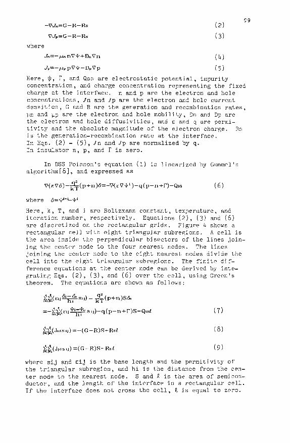
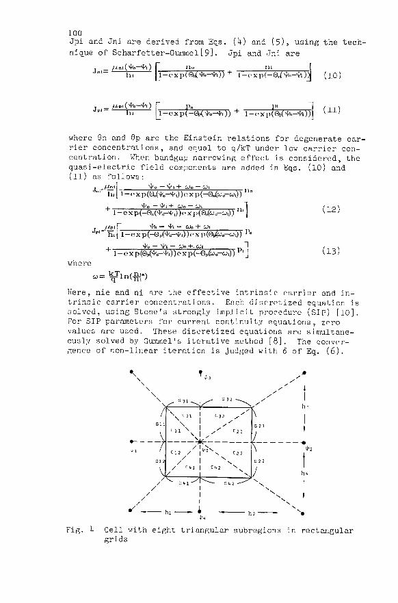
Here, k, T, and i are Boltzmann constant, temperature, and iteration number, respectively. Equations (2), (3) and (6) are discretized on the rectangular grids. Figure h shows a rectangular cell with eight triangular subregions. A cell is the area inside the perpendicular bisectors of the lines joining the center node to the four nearest nodes. The lines joining the center node to the eight nearest, nodes divide the cell into the eight triangular subregions. The finite difference equations at the center node can be derived by integrating Eqs. (2), (3), a.nd (6) over the cell, using Green's theorem. The equations are shown as follows:
=-gJi(£u^^Sii)-q(p-n + r)S-Qssi (7)
t£ (J„isij)=-(G-R)S4-Rsi (8)
iit( Jp.su) =(G-R)S-Rsi (9)
where sij and eij is the base length and the permitivity of the triangular subregion, and hi is the distance from the center node to the nearest node. S and £ is the area of semiconductor, and the length of the interface in a rectangular cell. If the interface does not cross the cell, £ is equal to zero.
100
Jpi and Jni are derived from Eqs. (U) and (5), using the tech
nique of Scharfetter-Gummel[9]. Jpi and Jni are
hi i-oxp(<=u *>-*i)) + i_t.xp(_<=u: *„-*))] (10
j p i _ / i p i ( > f e - * i )
l—exp(—1 •etC*. *.)) l-<-xp(0>{ *>-*,))] f 1 1)
where 6n and 9p are the Einstein relations for degenerate carrier concentrations, and equal to q/kT under low carrier concentration. When bandgap narrowing effect is considered, the quasi-electric field components are added in Eqs. (10) and (11) as follows:
•j-it; l-<-xp(a,(*„-*,))(-xp(-0„(£Jo-a),))n° , ^ o — <JM + CJo — u/i
l-oxp(-0„( o-+,))oxp(a/coo-cj1))
/LtpiF 'fe — Nh — ofe + coi J p l* h . [_ l -exp(-0p(+i , - - I ' . ) )«-xp(0^ . -c jO) P°
, +b — ^ 1 — CJD + . CJi 1 l -exp(eP(^„-4 '1))cxp(H9p(cj„-cj , )) ' ' J
( 1 2 )
( 1 3 )
w h e r e
, , _ k T i _ / n i . \
Here, nie and ni are the effective intrinsic carrier and intrinsic carrier concentrations. Each dincretized equation is solved, using Stone's strongly implicit procedure (SIP) [10]. For SIP parameters for current continuity equations, zero values are used. These discretized equations are simultaneously solved by Gummel's iterative method [8]. The convergence of non-linear iteration is judged with 6 of Eq. (6).
«v
\ ^ s "
/ I S
/ Em I Ci,2
/ :;m 37kr
L
St* 2 - - ^ \
/ / /
h i
1/J2
hu
h i h ; •
Fig. h Cell with eight triangular subregions in rectangular grids
101 U,2 The method setting initial conditions
The initial conditions for the numerical solution of Eq. (6) are prepared by depletion layer analysis or by extrapolation. In depletion layer analysis, Poisson's equation is simplified as
V(eV40=-qr-Qss (1*0
in insulator and depletion layer of semiconductor. The constant value of \jj is used in other regions of semiconductor. Equation (lU) is solved with the successive overelaxation. This method does not require an initial condition for itself, and can be used to approximate solutions of Poisson's equation for any device structure. DSS estimates the electrostatic potential by extrapolation if the electrode voltage changes successively during simulation, for example, calculation of I-V characteristics. The changes in electrostatic potential distributions are estimated from the electric field for the latest solutions in successive simulations. The initial conditions for electron and hole concentrations are calculated from electrostatic potential and fermi levels on the ohmic electrodes.
Boundary conditions are given as hold values for ohmic electrode and Schottky electrode. The conditions of charge neutality and thermal equilibrium are applied to ohmic electrodes. Interpolation method, one dimensional solution, and free boundary can be also set.
1».3 Physical models
DSS uses the physical models as shown below. Avalanche generation (G), bulk Shockley-Read-Hsll recombination ( RSHR ), and Auger recombination (K») are modeled using the equations as follows:
G=anUI+aPk/Pl (15)
R=RSHB + RA (16)
Rsim=(np-nf.)/['!rj(p+pO+T^n + iii)l (17)
RA=(np-nu)(Cnn+CPp) (l8)
where pi, nj, Cn, and Cp are parameters, a and T are the ionization rate[11] and carrier lifetime, respectively, given by
a = Aexp(-B\J\/\E-J\) (19)
and
T = Tmln +(Tm.,-Tml n)/(l+(r/rof) (20)
Here, A, B, xmin, Tmax, g, and To are parameters. At the surface, surface Shockley-Read-Hall model (Rs) is expressed by

102 Rs=(np-nu)/[(p+p0/S„+(n + ni)/fe,3 (21)
where Sn and Sp are parameters. The effective intrinsic carrier concentration due to the effect of bandgap narrowing[l2] is expressed as
n,.=n i exp(^(lnU+^lng+C )) (22)
where No, Vi, and C are parameters. The relationship( 13) between diffusivity and mobility is approximated by
E-/J.- q LI+4(NC) n r o ^ w J {23)
where nc and Nc are the carrier concentration and parameter, respectively. Carrier mobility models use Scharfetter and Gummel's expression[ 9] including Thornber's scaling law[l*4] for bipolar devices and Yamaguchi's model[15] for MOS devices, respectively.
^*h(£0S)+^<^S (2k) where
/i„>=/a. v/ l+r/(r /S+N r) (25)
for b ipolar dev ices , and
/iN.= «\/(i + r/(r/s+Nr))(i+E/E^ (26)
for MOS devices. Here, EJ. and E// are components of the electric field perpendicular and parallel to the current density vector, and vc, vs, S, Nr, Eo and Uo are parameters.
5. APPLICATIONS OF THE DEVICE SIMULATION
The device simulation program with the free step design method was tested with various semiconductor devices.
Typical n-channel MOSFETs were first simulated under the simulation procedure as shown in Table 1. This device has a gate length of 2.0 microns, a gate oxide thickness of 0.03 microns, and the junction depth of 0.3 microns under the source and drain electrodes. DSS receives both data of device structure as shown in Fig. 3 and a sequence of six steps from PPDS, and operated as stated below. In the first step, the Poisson's equation is solved rapidly by depletion layer analysis. Electron concentration and electrostatic potential are analyzed to approximate the true solutions. Next, the hole concentration, generation, and recombination are included into the simulation. In the last step, the electron and hole concentrations are solved to enhance the accuracy of the electrode currents. The bandgap narrowing effect, and the

Einstein relation for degenerate carrier concentration are not used in this simulation.
Figure 5 shows the I-V characteristics obtained according to this procedure. Solid lines and circles are experimental data and simulation results, respectively. The simulation results are in good agreement with experimental data when the coefficient of E0 in Eq. (26) is fitted at one point in the saturation region. This program can be simulated by two-carrier analysis under the condition of avalanche breakdown. Computation time per bias point was about 3 minutes for a 3-MIPS computer where the number of nodes was 1800 points , and the gate, drain, and substrate voltages were 3.0, k.O and 0.0 volts, respectively.
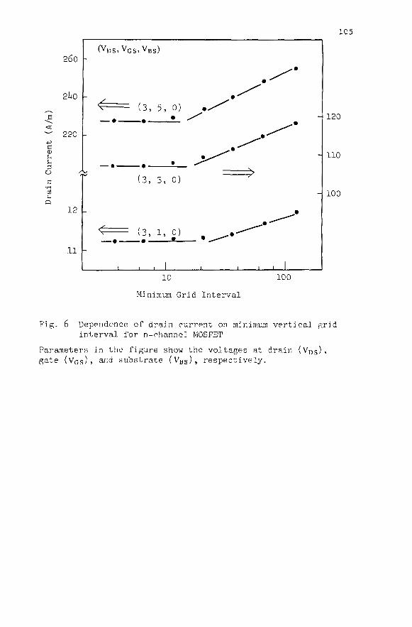
Figure 6 shows the dependence of the drain current on the minimum vertical grid interval. The drain currents increase due to the discretization error as the grid interval widens. This error is negligible for intervals of less than 10 angstroms. The discretization error for horizontal grid interval was also investigated and found independent of the interval.
Figure 7 shows the distribution on the electrostatic potential, both electron and hole concentrations and generation rate in the avalanche phenomena for VGS = +.0V, VDs = 7.5V, and V Bs
= 0V. Figure 8 shows the electrostatic distribution in the n-channel K0SFET with four gate electrodes, which is a delay line in the CCD senser. DSS uses step design for one-carrier analysis as shown in Table 2 because this device is operated in the bias condition where the static currents do not occur. In this case, DSS was executed with a computation time of less than 1 minute, which is comparable to the speed of an exclusive simulator. Figure 9 shows the electrostatic potential distribution for a typical npn-bipolar transistor. The bandgap narrowing effect is considered in device simulation. This program was found useful for applications to various devices.
6. CONCLUSION
To realize a useful device simulation program for arbitrary device structure and general analysis it is important and effective that the device simulator is independent of the device structure. The pre-processor must operate the user interface exclusively. Device simulator performs numerical solution according to input data sent from the pre-processor. The input data is a sequence of design steps and informations about nodes and boundaries. In each design step, solved equations, physical models, and convergence conditions are specified. The combination of these steps enabled device simulation to find a better numerical solution in the less computation time. Depletion layer analysis was effective for setting initial conditions for numerical solution independent of the

lOh device structure. The device simulation program developed with the algorithms above proved to be applicable to many devices, and expected to be used in the research and development of VLSI devices.
Table 1
Step designs for n-channel MOSFET
STEP
1
2
3
It
5
6
VARIABLE
i> ty, n
<K n , p
ty, "> P ijj, n , p
n , p
PHYSICAL MODEL
G
G, R
G, R
CONVERGENCE CONDITION
Aij; = 1 0 " 2 V
Alp = 1 0 " 3V
AiJ> = 1 0 " 3V
Aijj = 1 0 " " v
AIJJ = 1 0 " MV
^ = ^ i = i o - 5
n p
O Simulation
0 2.0 U.0 6.0 8.0
Drain Voltage (V)
F i g . 5 I-V c h a r a c t e r i s t i c s of n - c h a n n e l MOSFET ( S u b s t r a t e v o l t a g e i s 0 .0V. )
105
e < • p
d
o
Q
260
2l+0
220
12
11
(V„S,VGS,VBS)
( 3 , 3, 0)
( 3 , 1, 0}
_j 1 1 _l L.
- 120
110
100
10 100
Minimum Grid In t e rva l
Fig. 6 Dependence of drain current on minimum v e r t i c a l grid i n t e r v a l for n-channel MOSFET
Parameters in the f igure show the vol tages at drain (VD S) , gate (VGS) » a r 'd s u b s t r a t e (V B S ) , r e spec t ive ly .

106
(A) Electrostatic potential distributic
% > •
(B) Electron concentration distribution

107
o • . • V* (C) Hole concentration distribution
(D) Generation rate distribution
F i g . 7 Avalanche phenomena in t h e n - c h a n n e l MOSFET a t VGs= U.OV, V D S =7 .5V, and VB S=0.0V

108 Table 2
Step designs for n-channel MOSFET with four gate electrodes
STEP
1
2
VARIABLE
* \\>, n
PHYSICAL MODEL CONVERGENCE CONDITION
AIJJ = 10"2V
Ail = 10""v
Fig. 8 Electrostatic potential distribution in n-channel MOSFET with four gate electrodes where VDS=o .IV, VGsi =-1.0V, VGS2=-1.0V, V G S S ^ ^ - O V , VGS4=-^.0V, and VBS = -5.0V, respectively.

109
^ .^
«. .^ ^ .^
1. .^
Fig. 9 Electrostatic potential distribution for typical npn-transistor where VBE=0-7V and VCE=0.5V.
ACKNOWLEDGEMENT
The authors wish to thank Y. Namba, S. Baba, K. Nishi, and T. Yamaji of OKI Electric Industry Co., Ltd. for their discussion and support.
REFERENCES
1. Mock, M.S. "A two-dimensional mathematical model of the insulated-gate field-effect transistor" Solid-State Electron., vol. l6, p. 601, 1973-
2. Toyabe, T. and Asai, S. "Analytical models of threshold voltage and breakdown voltage of short-channel MOSFET's derived from two-dimensional analysis" IEEE J. Solid-State Circuits, vol. SC-lU., p. 375, 1979-
3. Sano, E., Kasai, R., Ohwada, K. and Ariyoshi , H. "A two-dimensional analysis for MOSFET's fabricated on buried Si02 layer" IEEE Trans. Electron Devices, vol. ED-27, p. 201*3, 1980.
h. Engl, W.L. , Dirks, H.K. and Meinerzhagen, B. "Device modeling" Proc. IEEE, vol. 71, p. 10, 1983-

Selberher r , S . , Schiitz, A. and P o t z l , H.W. "MINIMOS-A two-dimensional MOS t r a n s i s t o r analyzer" IEEE Trans. Electron Devices, vol . ED-27, p. 15l*0, 1980.
Watanabe, D.S. and Slamet, S. "Numerical simulation of ho t -e l ec t ron Phenomena" IEEE Trans. Electron Devices, vo l . ED-30, p . 10l»2, 1983.
N i sh i , K., Sakamoto, K. and Ushio, S. "Process s imulat ion of mul t i l ayer s t r u c t u r e s involving p o l y c r y s t a l l i n e and s i l i c o n n i t r i d e " Ext. Abstr . ECS Fal l Meeting I98I Denver, p . 998, I98I .
Gummel, H.K. "A s e l f - c o n s i s t e n t i t e r a t i v e scheme for one-dimensional steady s t a t e t r a n s i s t o r ca l cu l a t ions" IEEE Trans. Electron Devices, vo l . 1 1 , p . 1»55, 196^.
S c h a r f e t t e r , D.L. and Gummel, H.K. "Large-signal ana lys is of a s i l i c o n read diode o s c i l l a t o r IEEE Trans. Electron Devices, vol. ED-16, p. 6k, I969.
Stone, H.L. "Iterative solution of implicit approximations of multidimensional partial differential equations" SIAM J. Humer- Anoi. , vol. 5-, P- 530, 1968.
Grant, W.N. "Electron and hole ion iza t ion r a t e s in e p i t a x i a l s i l i con at high e l e c t r i c f i e l d s " So l id -S ta te E l e c t r o n . , vo l . 16, p . I I 8 9 , 1973.
Slotboom, J.W. and De Graaff, H.C. "Measurements of bandgap narrowing in Si b ipo la r t r a n s i s t o r s " So l id -S ta te E l e c t r o n . , vo l . 19, P- 857, 1976.
Kroemer, H. "The Eins te in r e l a t i o n for degenerate c a r r i e r concentrat i o n s " IEEE Trans. Electron Devices, vo l . ED-25, p . 850, 1978.
Thornber, K.K. "Relation of d r i f t ve loc i ty to low-f ie ld mobil i ty and h igh - f i e ld s a tu ra t i on ve loc i ty" J. Appl. Phys., vol. 51, p. 2127, 1980.
Yamaguchi, K. "A mobility model for carriers in the MOS inversion layer IEEE Trans_. Electron Devices, vol. ED-30, p. 658, 1983.
Related Documents