Two Dimensional DCT/IDCT Architecture Authors: A. Aggoun and I. Jalloh Address: Faculty of Computing Sciences and Engineering. De Montfort University, The Gateway Leicester LE1 9BH. Contact: Dr. A. Aggoun Tel: +44 (0)116 2577055 Fax: +44 (0)116 2577692 Email: [email protected]

Welcome message from author
This document is posted to help you gain knowledge. Please leave a comment to let me know what you think about it! Share it to your friends and learn new things together.
Transcript

Two Dimensional DCT/IDCT Architecture
Authors: A. Aggoun and I. Jalloh
Address: Faculty of Computing Sciences and Engineering.
De Montfort University, The Gateway Leicester LE1 9BH.
Contact: Dr. A. Aggoun
Tel: +44 (0)116 2577055
Fax: +44 (0)116 2577692
Email: [email protected]
2
Abstract:
A new fully parallel architecture for the computation of a two-dimensional (2D) discrete cosine
transform (DCT), based on the row-column decomposition is presented. It uses the same one-
dimensional (1D) DCT unit for the row and column computations and (N2+N) registers to
perform the transposition. It possesses features of regularity and modularity, and is thus well
suited for VLSI implementation. It can be used for the computation of either the forward or the
inverse 2D DCT.
Each 1D DCT unit uses N fully parallel vector inner product (VIP) units. The design of the VIP
units is based on a systematic design methodology using radix-2n arithmetic, which allows
partitioning of the elements of each vector into small groups. Array multipliers without the final
adder are used to produce the different partial product terms. This allows a more efficient use of
4:2-compressors for the accumulation of the products in the intermediate stages and reduces the
numbers of accumulators from N to 1. Using this procedure, the 2D DCT architecture requires
less than N2 multipliers (in terms of area occupied) and only 2N adders. It can compute a N×N-
point DCT at a rate of one complete transform per N cycles after an appropriate initial delay.
3
Introduction:
The discrete cosine transform (DCT) has emerged as the most popular transform for many
image/video compression applications owing to its near optimal performances compared to the
statistically optimal Karhunen-Loeve transform [1]. Its energy compaction efficiency is also
greater then any other transform. The 2D DCT, in particular, is one of the major operations in
current image/video compression standards [2-5]. It is today the most widely used orthogonal
transform for applications including videophone, video conferencing and high definition
television.
The 2D DCT is computationally intensive and as such there is a great demand for high speed,
high throughput and short latency computing architectures. Due to the high computation
requirements, the 2D DCT processor design has been concentrated on small nonoverlapping
blocks (typical 8x8 or 16x16). Many 2D DCT algorithms have been proposed to achieve
reduction of computational complexity and thus increase the operational speed and throughput.
The various algorithms and architectures for the 2D DCT can be divided into two categories: the
row-column decomposition methods and the non-row-column decomposition methods.
Several hardware design methods for the implementation of the 2D DCT have been developed
in recent years [6-9]. Hsia et. al [6] reported an algorithm and architecture to calculate the 2D
inverse DCT (IDCT) directly by skipping the zero DCT coefficients, since they do not affect the
transform results of the IDCT. The IDCT algorithm is realised by a pipelined architecture and
modular design and it utilises pipelined combinational multipliers to decrease the critical path.
The implementation uses relatively less hardware to achieve sufficient speed for real
applications. It achieves an average pixel rate varying from 150 MHz to a maximum pixel rate
of 400 MHz when using a 50 MHz clock. The main advantage of the architecture is that it uses a
lower operation frequency to obtain a very high pixel rate. However, the disadvantage of this
4
architecture is that it can only perform the inverse DCT. This is because it utilises the fact that in
many image coding systems, most of the DCT coefficients are quantised to zeros and that in
interframe coding the nonzero coefficients is even smaller due to the motion compensation in
sequential images. As such this system cannot be used to implement both the DCT and IDCT
using the same hardware.
Chiang et. al [7] reported a 2D DCT/IDCT architecture which utilises the overlapped row-
column operation, instead of the transpose memory, in order to reduce the total latency of the
structure. The core processor is organised into two cascaded 1D DCT/IDCT units and one
control unit. The multiplication block is implemented by using look-up tables. In order to reduce
the size of the table, the precalculated partial products of the DCT/IDCT coefficients and the
input data are stored in two separate tables. By avoiding the use of multipliers and the transpose
RAM the architecture can achieve an operation speed of up to 100 MHz. The disadvantage of
this architecture is that different structures are used for the computation of the two 1D DCT
blocks.
Fernández et. al [8] reported an 8×8 2D DCT processor using the row-column decomposition
method, based on the residue number system (RNS). The processors utilise a fast cosine
transform algorithm that requires a single multiplication stage for each signal path. Thus each
1D DCT block consists of 14 multipliers and 32 adders and subtractors. Linear combinations of
the DCT coefficients are precalculated and stored in ROMs, thus the DCT can be calculated
with look-up table multipliers. The transposition unit consists of an 8×8 matrix of registers and
multiplexers interconnected to allow the transposition of parallel input data. One of the
drawbacks of this system is the practical implementation of RNS-based systems, which
possesses serious limitations in the conversion stage. RNS-to binary conversion requires the use
5
of 32-bit (since the input data and the selected moduli are 8-bit width) word-length adders and
large multipliers thus resulting in more hardware and degradation of system performance.
Chang and Wang [9] reported an implementation of the 2D DCT/IDCT based on the row-
column decomposition and uses a systolic array without the matrix transposition hardware. The
system is achieved in three steps and requires N2 multipliers and N2+3N adders. With a
throughput rate of one N×N-point DCT per N cycle and a pixel rate of about 320MHz, it has a
good area-time performance and it is very attractive for very high-speed applications. However,
the significant drawbacks in this work is that the architecture is not modular, it uses different
structures to achieve the two 1D DCT blocks and different structures for computing the forward
and the inverse 2D DCT.
In this paper, a new fully parallel 2D DCT/IDCT architecture using the linear systolic matrix-
vector without the RAM based matrix transposition is presented. It is shown that the architecture
is highly modular, parallel and can be used to compute both the forward and the inverse 2D
DCT. Finally, it is shown that the proposed architecture enables the realisation of the 2D DCT
with a relatively smaller hardware compared to the conventional approaches, and it also results
in an extremely regular structure such that its realisation is very simple. A new transposition
matrix is introduced which uses (N2+N) registers and N (N:1) multiplexers. This allows the
reading of N output coefficients from the 1st 1D DCT and the feeding of N coefficients to the 2nd
1D DCT in a pipelined fashion. Also, a systematic methodology, which allows the design the
vector inner products used to implement the matrix-vector multiplier is presented. It is based on
the radix-2n arithmetic which allows partitioning of the operands to n-bit digits each and hence
providing the designer with more flexibility between throughput rate and hardware cost, by
varying the digit-size n, the pipelining level and also the type of architecture. In this paper, the
radix-2B/4 vector inner product architecture is described and is used within the 2D DCT

6
architecture, where B is the data wordlength. The resulting 2D DCT architecture is compared to
previously reported architectures.
1. The 2D DCT Algorithm
For a given 2D spatial data sequence {Xij; i, j = 0, 1, … , N-1}, the 2D DCT data sequence {Ypq
; p, q = 0, 1, … , N-1} is defined by:
N
qjN
piX
NEEY
N
i
N
jijqppq ��
−
=
−
=��
���
� +��
���
� +=1
0
1
0 2)12(
cos2
)12(cos
2 ππ (1)
where
�
≠==
0x ,
0x , E x
121
The forward and inverse transforms are merely mappings from the spatial domain to the
transform domain and vice versa. The DCT is a separable transform and as such, the row
column decomposition can be used to evaluate equation (1). Denoting: 2
)12( cos ��
���
� +N
lh πby clh
and neglecting the scale factor qp EEN2
, the column transform can be expressed as:
1N ,... 2, 1, 0, q p,cZYN
jqjpjpq −==�
−
= ,
1
0
(2)
and the row transform can be expressed as:
1N ,... 2, 1, 0, j p,cXZN
ipiijpj −==�
−
= ,
1
0
(3)
In order to compute an N x N-point DCT (where N is even), N row transforms and N column
transforms need to be performed. However, by exploiting the symmetries of the cosine function,
the number of multiplications can be reduced from N2 to N2/2. In this case, each row transform
given by equation (3) can be written as matrix-vector multipliers via,
7
�−
=−−−+=
1
0)1(
2
])1([N
ipijiN
pijpj cXX Z (4)
Using a matrix notation, for N=8, equation (4) can written as
����
�
�
����
�
�
++++
����
�
�
����
�
�
=
����
�
�
����
�
�
4030
5020
6010
7000
63626160
43424140
23222120
03020100
60
40
20
00
XXXX
XXXX
cccccccc
cccccccc
ZZ
ZZ
(5)
����
�
�
����
�
�
−−−−
����
�
�
����
�
�
=
����
�
�
����
�
�
4030
5020
6010
7000
73727170
53525150
33323130
13121110
70
50
30
10
XXXX
XXXX
cccccccc
cccccccc
ZZ
ZZ
(6)
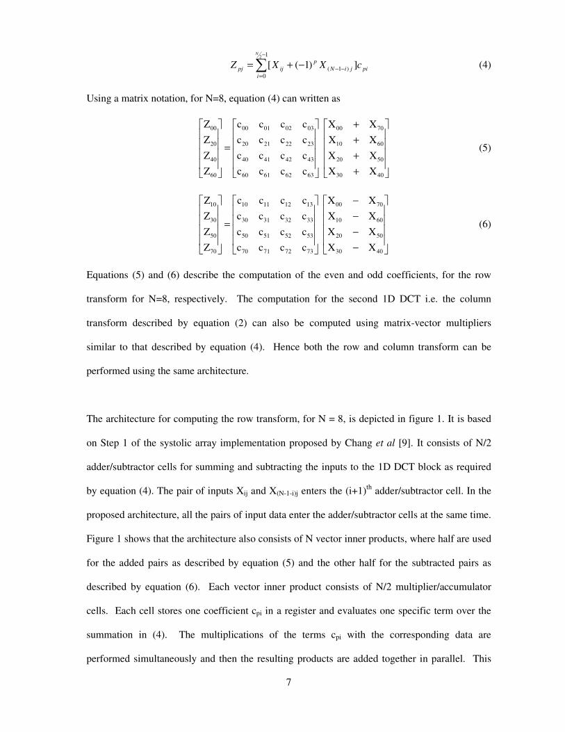
Equations (5) and (6) describe the computation of the even and odd coefficients, for the row
transform for N=8, respectively. The computation for the second 1D DCT i.e. the column
transform described by equation (2) can also be computed using matrix-vector multipliers
similar to that described by equation (4). Hence both the row and column transform can be
performed using the same architecture.
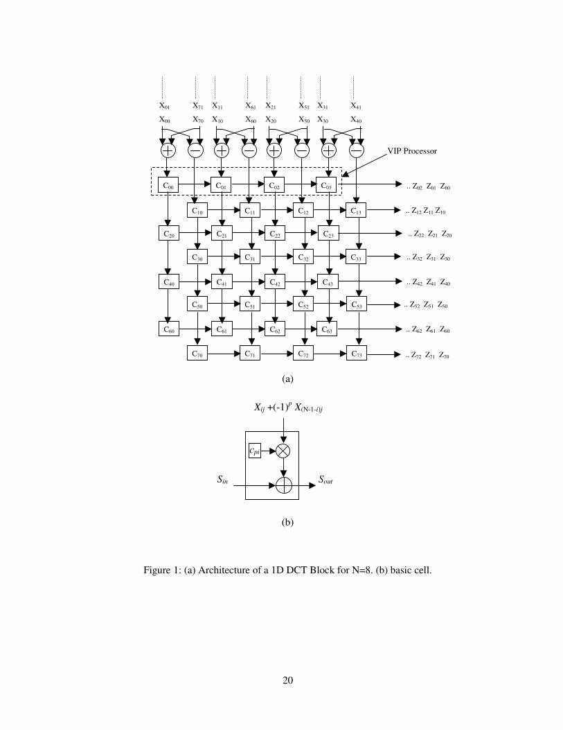
The architecture for computing the row transform, for N = 8, is depicted in figure 1. It is based
on Step 1 of the systolic array implementation proposed by Chang et al [9]. It consists of N/2
adder/subtractor cells for summing and subtracting the inputs to the 1D DCT block as required
by equation (4). The pair of inputs Xij and X(N-1-i)j enters the (i+1)th adder/subtractor cell. In the
proposed architecture, all the pairs of input data enter the adder/subtractor cells at the same time.
Figure 1 shows that the architecture also consists of N vector inner products, where half are used
for the added pairs as described by equation (5) and the other half for the subtracted pairs as
described by equation (6). Each vector inner product consists of N/2 multiplier/accumulator
cells. Each cell stores one coefficient cpi in a register and evaluates one specific term over the
summation in (4). The multiplications of the terms cpi with the corresponding data are
performed simultaneously and then the resulting products are added together in parallel. This
8
addition is carried out using carry save arithmetic modules incorporated within the multipliers
structure as will be described is section 4.
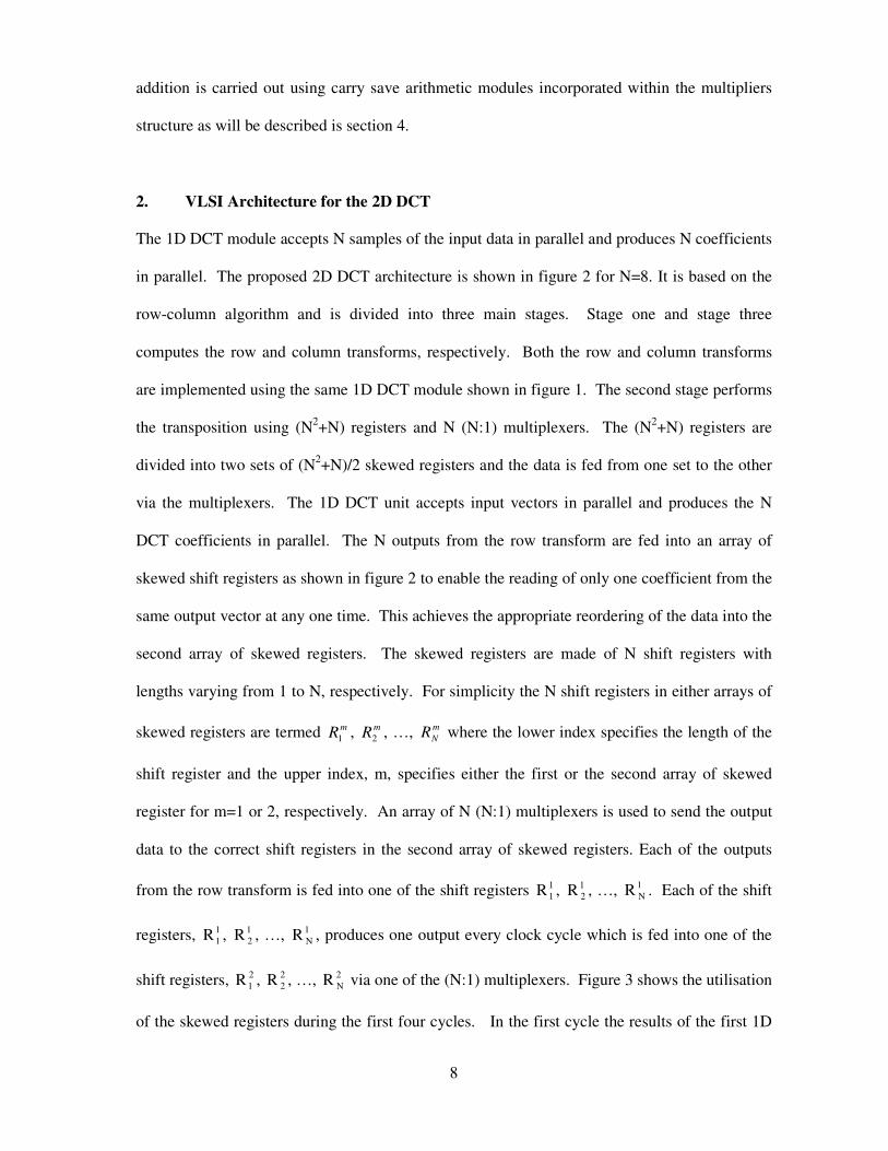
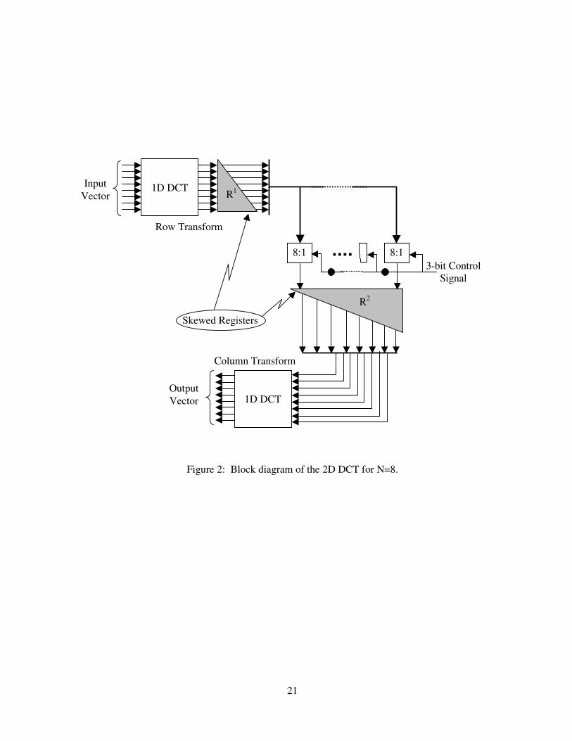
2. VLSI Architecture for the 2D DCT
The 1D DCT module accepts N samples of the input data in parallel and produces N coefficients
in parallel. The proposed 2D DCT architecture is shown in figure 2 for N=8. It is based on the
row-column algorithm and is divided into three main stages. Stage one and stage three
computes the row and column transforms, respectively. Both the row and column transforms
are implemented using the same 1D DCT module shown in figure 1. The second stage performs
the transposition using (N2+N) registers and N (N:1) multiplexers. The (N2+N) registers are
divided into two sets of (N2+N)/2 skewed registers and the data is fed from one set to the other
via the multiplexers. The 1D DCT unit accepts input vectors in parallel and produces the N
DCT coefficients in parallel. The N outputs from the row transform are fed into an array of
skewed shift registers as shown in figure 2 to enable the reading of only one coefficient from the
same output vector at any one time. This achieves the appropriate reordering of the data into the
second array of skewed registers. The skewed registers are made of N shift registers with
lengths varying from 1 to N, respectively. For simplicity the N shift registers in either arrays of
skewed registers are termed mR1 , mR2 , …, mNR where the lower index specifies the length of the
shift register and the upper index, m, specifies either the first or the second array of skewed
register for m=1 or 2, respectively. An array of N (N:1) multiplexers is used to send the output
data to the correct shift registers in the second array of skewed registers. Each of the outputs
from the row transform is fed into one of the shift registers 11R , 1
2R , …, 1NR . Each of the shift
registers, 11R , 1
2R , …, 1NR , produces one output every clock cycle which is fed into one of the
shift registers, 21R , 2
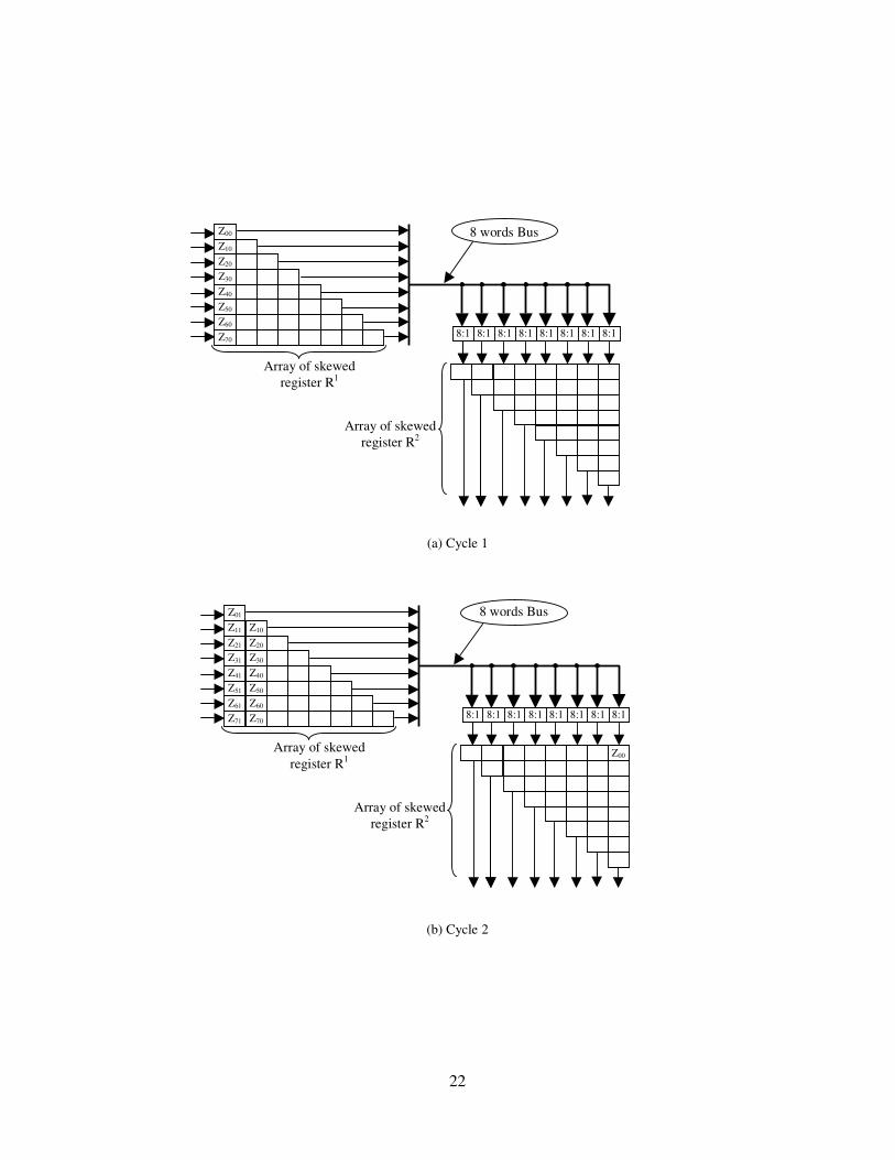
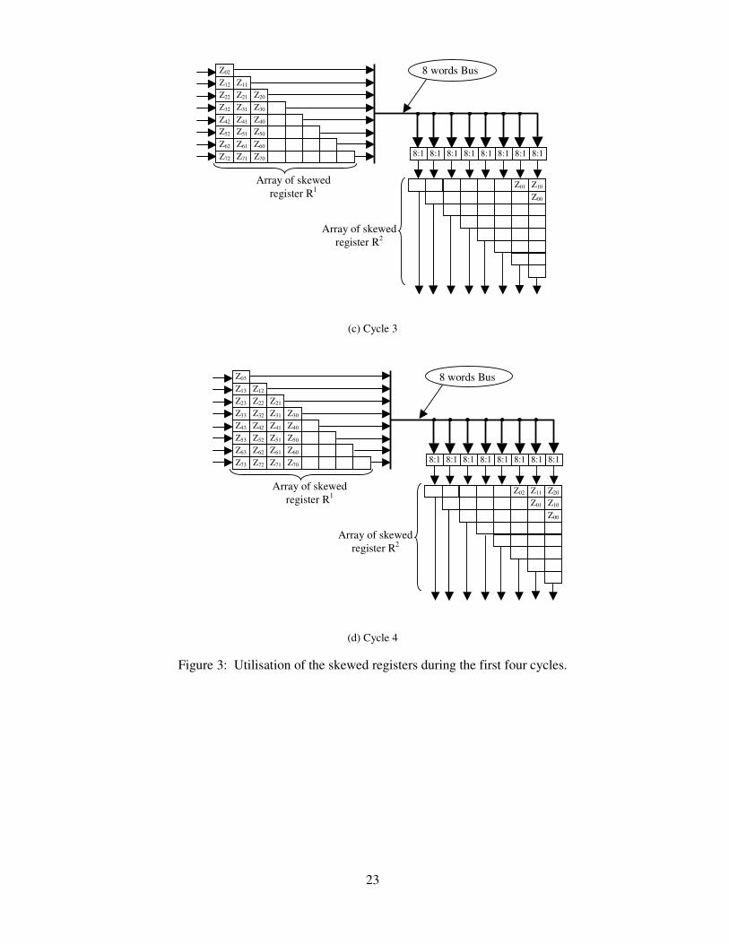
2R , …, 2NR via one of the (N:1) multiplexers. Figure 3 shows the utilisation
of the skewed registers during the first four cycles. In the first cycle the results of the first 1D
9
DCT are stored in R1 as shown in figure 3a. During the second cycle, the data from 11R (i.e. Z00)
is fed into the shift registers 2NR (see figure 3b). In the third cycle the data from 1
1R (Z01) is fed
into 21−NR and the data from 1
2R (Z10) is fed into 2NR (see figure 3c). In the fourth cycle, the
data from 11R (Z02) is fed into 2
2−NR , the data from 12R (Z11) is fed into 2
1−NR and the data from
13R (Z20) is fed into 2
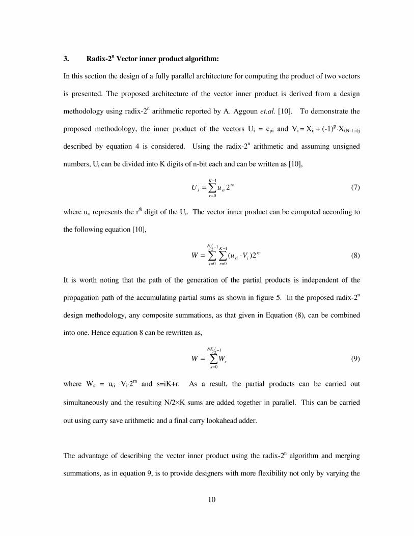
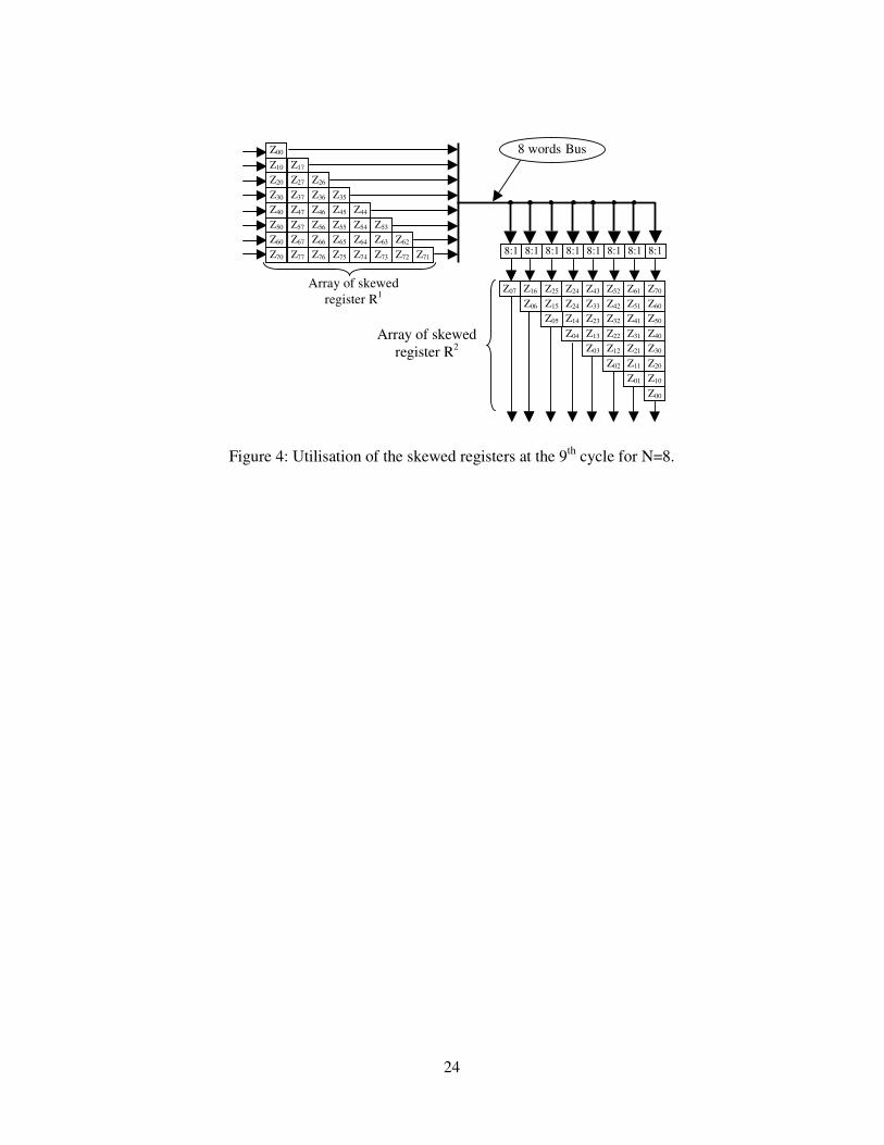
NR (see figure 3d). This process is continued until the entire data is
transferred. At the (N+1)th cycle the data from 11R (Z0,N-1) is fed to 2
1R , while the data from 1NR
(ZN-1,0) is fed into 2NR . At this point, the N point data incoming from the first VIP or register 1
1R
is available at the output of the registers 21R , 2
2R , …, 2NR and ready to enter the column
transform as shown in figure 4 for N=8. In the following cycle the data from the second VIP or
the register 12R is ready to enter the column transform, while the data from the first VIP or
register 11R is being processed by the second 1D DCT. This process continues till all the
remaining coefficients in the skewed registers 2R have entered the column transform. Hence
after an initial delay of (N+1) cycles, the proposed architecture will output N 2D DCT
coefficients every clock cycle. Whilst the 1D DCT coefficients stored in the array of skewed
registers R2 are being processed by the second 1D DCT block, the transfer from the first 1D
DCT block into the array of the skewed registers R2 via the array of skewed registers R1 and the
array of multiplexers continues until all the input data has been processed.
For N=8, a 3-bit control signal is required to enable the 8:1 multiplexers to select one of the
eight input words. During the first cycle of the transfer of data from R1 to R2, the first
multiplexer from the right will select its port 1 as its output. In the second cycle, the second
multiplexer on the right will select port 1 as its output while the first multiplexer from the right
will select port 2 as its output and so on. Hence, the control signal is connected to all
multiplexers through delay elements as shown in figure 2.
10
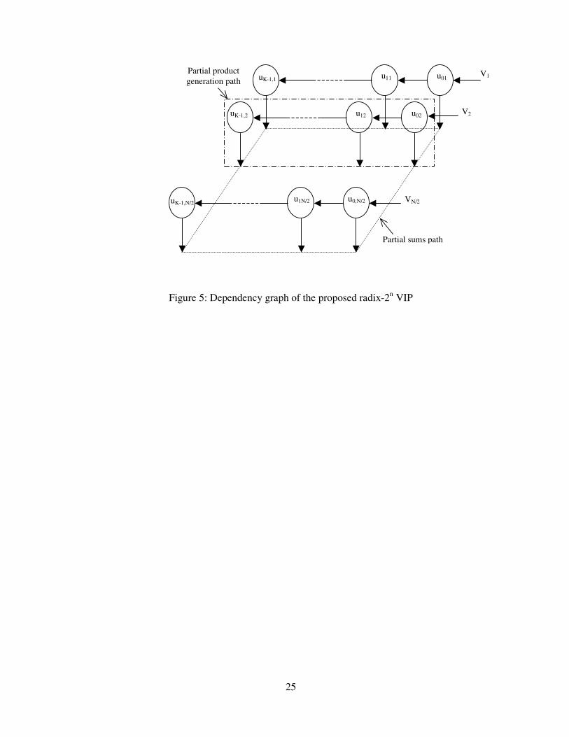
3. Radix-2n Vector inner product algorithm:
In this section the design of a fully parallel architecture for computing the product of two vectors
is presented. The proposed architecture of the vector inner product is derived from a design
methodology using radix-2n arithmetic reported by A. Aggoun et.al. [10]. To demonstrate the
proposed methodology, the inner product of the vectors Ui = cpi and Vi = Xij + (-1)p�X(N-1-i)j
described by equation 4 is considered. Using the radix-2n arithmetic and assuming unsigned
numbers, Ui can be divided into K digits of n-bit each and can be written as [10],
�−
==
1
0
2K
r
rnrii uU (7)
where uri represents the rth digit of the Ui. The vector inner product can be computed according to
the following equation [10],
� �−
=
−
=
⋅=12
0
1
0
2)(N
i
K
r
rniri VuW (8)
It is worth noting that the path of the generation of the partial products is independent of the
propagation path of the accumulating partial sums as shown in figure 5. In the proposed radix-2n
design methodology, any composite summations, as that given in Equation (8), can be combined
into one. Hence equation 8 can be rewritten as,
�−
=
=12
0
NK
ssWW (9)
where Ws = uri ⋅Vi⋅2rn and s=iK+r. As a result, the partial products can be carried out
simultaneously and the resulting N/2×K sums are added together in parallel. This can be carried
out using carry save arithmetic and a final carry lookahead adder.
The advantage of describing the vector inner product using the radix-2n algorithm and merging
summations, as in equation 9, is to provide designers with more flexibility not only by varying the
11
digit size n, but also in the way the accumulation of the partial sums is carried out. This is evident
when it is realised that there are numerous ways in which the summation in equation (9) can be
decomposed; the decomposition in equation (8) being only one of those. In other words, the sum in
equation (9) can be split into several nested sums where each sum can be carried out in an
independent way using either a tree or a liner structure. Each one of these different mappings would
lead to a different architecture with its own are-time complexity. As an example, the conventional
word level VIP architecture is obtained by splitting the summation in equation (9) into the two
summations in equation (8) and performing the summation over index r first. In this paper, a new
implementation is proposed which is derived without splitting the summation in equation (9).
4. Design of a two's complement parallel vector inner product:
In this section the architecture of a two’s complement radix-2B/4 VIP, where B is the data
wordlength, is discussed. The radix-2n VIP algorithm described by equation (8) assumes
unsigned numbers. In what follows, the two's complement array multiplication proposed by
Baugh and Wooley [11] is adapted to two’s complement radix-2n multiplication. Let consider
the multiplication of two B-bit two's complement numbers, where the multiplier and the
multiplicand, Ui and Vi, are written in the form
VvV
UuUBB
ii
BBii
~2
~2
11
11
+−=
+−=−−
−−
(10)
where U~ and V
~ are (B-1)-bit positive number comprising the B-1 least significant bits of Ui and Vi,
respectively, and 1−Biu and 1−B
iv are their most significant bits. Following the same procedure as in
[10] and [12], the multiplication of two B-bit two’s complement numbers, Ui and Vi, can be written
in a form involving only positive partial products provided that all partial products which involve a
sign bit and a nonsign bit are complemented. The final product is then obtained by adding a fixed
correction term to the final result, viz.,
12
121112211 222)~~(~~2)( −−−−−−− −+⋅⋅+⋅+⋅+⋅⋅=⋅ BBBBii
Biiii
BBi
Biii uVvUVUvuVU (11)
Two’s complement representation is adapted to normal multiplication by simply replacing the AND
with a NAND gate for all the partial product involving the sign bits, 1−Biu and 1−B
iv , as can be seen
from equation (11), except for the product 11 −− ⋅ Bi
Bi vu , which is carried out using an AND gate.
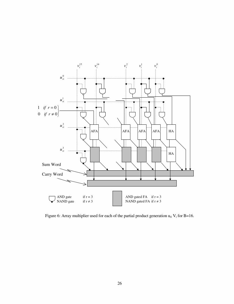
In the new implementation, each of the N/2×K products, Ws, is computed using the array multiplier
shown in figure 6 for B=16 and K=4. As can be seen in figure 6, the two top carry save adders
(CSAs) and the column of full adders (FAs) involving the sign bit 1−Biv required in conventional
array multipliers, are removed since they have empty bit positions. However, on the right hand side
of each array a column of half adders (HAs) is needed to add the two bits 10iri vu ⋅ and 01
iri vu ⋅ and
propagate the carry bits from the top to the bottom as shown in figure 6. Each array multiplier
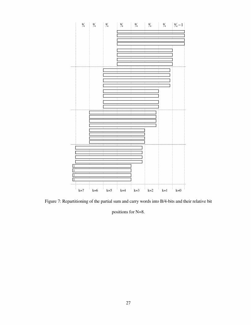
produces a (5B/4-1)-bit sum word and a B-bit carry word for K=4. As a result, N×K words are fed
into the accumulation path and arranged with respect to their significance as shown in figure 7 for
N/2=K=4.
The addition of the term -22B-1 is taken care of by adding a 1 to the most significant bit of the result
and the term 2B by adding a 1 to the (B+1)th column of the final result [4]. This is achieved by
extending the carry word of the products, iiK Vu ⋅− ,1 , by one nonzero bit as shown in figures 7 and 8
for the -22B-1 term and feeding a one into the empty bit position of the AND gated FA, ( 22,0
−⋅ Bii vu ),
of the array multiplier which computes the product ii Vu ⋅,0 for the term 2B, as shown in figure 6 for
B=16.
The partial sums and carries from all the N/2×K multipliers are accumulated together in parallel
using carry save arithmetic implemented with 4-2 compressors as shown in figure 8. The partial
13
sums and carries are repartitioned into digits of B/4-bit each as shown in figure 7. All the terms
with the same significance, k, are added together using an array of B/4-bit 4:2-compressors as
shown in figure 9 for k=4. The B/4-bit 4:2-compressors are obtained by interconnecting two B/4-bit
CSAs with fast input and output. The output from the first CSA with the longest path (i.e. path
through two XORs) is fed into the carry input of the second CSA. This makes the total delay
through the 4:2-compressors equivalent to three XORs. The critical path in the accumulation of the
partial sum and carry terms consists of four B/4-bit 4:2-compressors which is obtained for k=4 as
shown in figure 9. Hence, the longest delay in the accumulation of the all the sum and carry terms
is equivalent to that of six FAs.
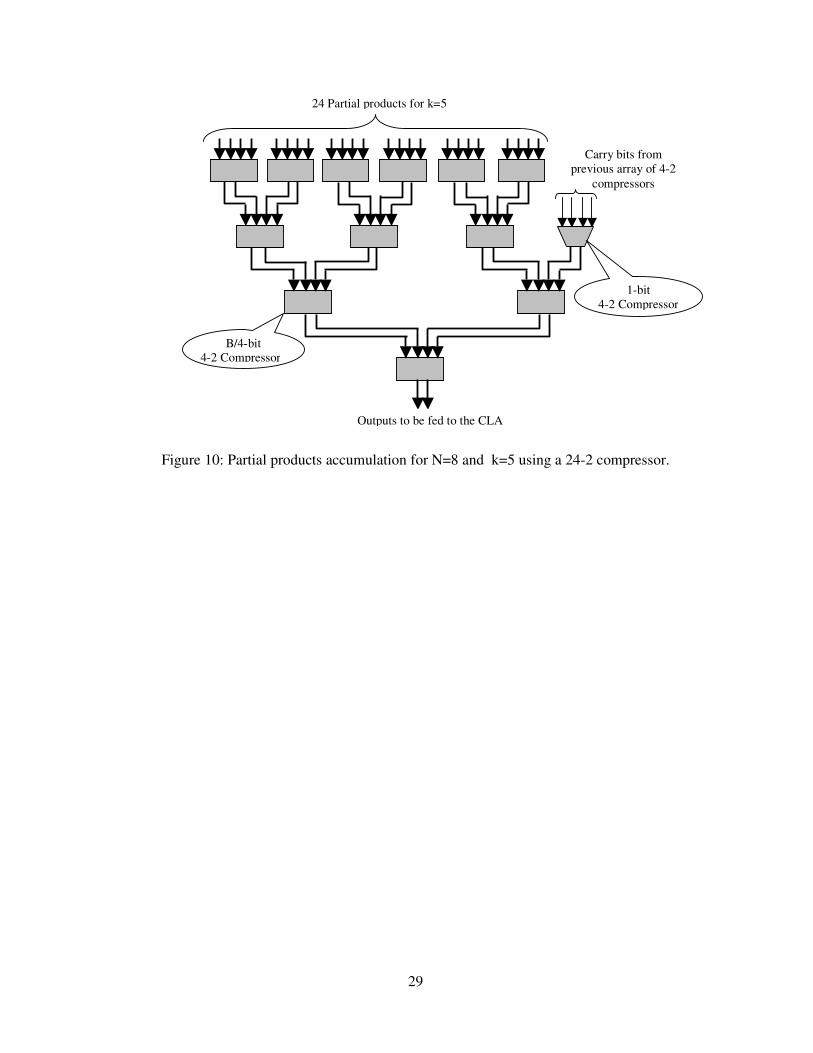
It is worth mentioning that carry bits are propagated between the array of 4-2 compressors from
right to left. Let Pk be the array used for the accumulation of all terms with the same significance,
k. For k < 4, the output carries from the array Pk are fed directly into the carry inputs of the array
Pk+1. However, for k ≥ 4, the number of carries generated by the array Pk is greater than the number
of carry inputs available to the array Pk+1. As a result, extra FAs and/or HAs are required to
accommodate the extra carries. This is shown as an example in figure 10 for k=5, where the array
P5 takes carries from P4. Each 4-2 compressor produces two 1-bit carry outputs and has one 1-bit
carry input. Furthermore, all the 4-2 compressor of the arrays Pk, except the ones in the top, will
have an extra two 1-bit empty position, which can accommodate carry bits. To compress 24 bits
into 2 bits, the array P5 would require a total of eleven 4-2 compressors, where six are in the top
row and five in remaining stages. Hence the array P5 can take up to 21 carry bits. However, the
array P4 will produce a total of 30 carry bits, one of which is fed to the carry look ahead adder and
the remaining 29 are fed into the array P5. To take care of the remaining eight carry bits, a 1-bit and
a B/4-bit 4-2 compressors are added to the array P5 as shown in figure 10. Similarly, 4-2
compressors are added to the arrays P6 and P7 to accommodate the extra carry bits from the array P5
and P6, respectively.
14
5. Performance analysis:
In this section, the performance of the proposed parallel 2D DCT architecture is compared with the
design proposed in [9]. The proposed architecture employs 2N vector inner product units and
parallel-in parallel-out I/O form. Each vector inner product unit are implemented using N/2
parallel multipliers without the final adder. The addition of the partial product from the N/2
multipliers is carried out in parallel and is embedded within the structure of the parallel multipliers.
One of the operands of each multiplier is divided into four groups, which produces four carry words
and four sum words. The total of 4N words are added together using carry save arithmetic
implemented with arrays of 4-2 compressors. The 4-2 compressors within each array are arranged
in a tree structure and used to add terms with the same significance. In what follows ACSA(N,B)
denotes the hardware cost required by the addition of the 2N (5B/4-1)-bit partial sum words and the
2N B-bit carry words using carry save arithmetic. Assuming a B-bit input data, one
(2B+log2(N/2)+1)-bit carry lookahead adder is required for each vector inner product unit. The 1D
DCT unit also requires N B-bit adder or subtractor units to add or subtract pairs of input data before
being fed into the vector inner products. Hence, the total cost of the 1D DCT unit is given by
( )( ) ( ) ( )���
���
�++��
�
���
�+��
��
�++−+= B,NABA12N
logB2AA2BBAB2N
N)N,B(A CSACLA2CLAFAAND2
DDCT1
where AAND, AFA and ACLA(B) are the area taken by an AND, an FA and a B-bit carry lookahead
adder. Assuming that the data is truncated to B-bit before entering the transposition buffer, which
is made of (N2+N)/2 registers and N B-bit 8:1 multiplexers. Each 8:1 multiplexers could be
implemented using a tree of seven 2:1 multiplexers. The cost of a B-bit 2:1 multiplexer is that of
3B AND gates. Hence the total cost of the buffer transposition unit is given by
)(2
21),( Re
2
BANN
NBANBA gANDbuffer
++=
15
where AReg(B) is the cost of a B-bit register. The total cost of the proposed 2D DCT architecture is
that of two 1D DCT units plus that of the buffer transposition unit, via
)N,B(A)N,B(A2)N,B(A bufferDDCT1DDCT2 +=
The 2D DCT architecture in [9] consists of three stages. The first stage consists of N B-bit adder or
subtractor units and N vector inner products. In conventional DCT implementation, the vector
inner products are usually implemented with a linear array of multiplier accumulators. To carry out
a fair comparison the parallel multipliers are implemented using the same structure as in [12]. In
this case, each vector inner product unit will require N/2 arrays of B/4-bit 4-2 compressors and N/2
(2B+1)-bit carry lookahead adders. Each array of 4-2 compressors will have a cost ACSA(1,B).
Also, N/2 (2B+1)-bit delay elements are required to be placed at the output of the multiply-
accumulator cells. Furthermore, N(N-2)/4 B-bit registers are required at the input of stage 1.
Hence, the total cost of the first stage of the architecture in [9] is given by
( )
( ) )(4
2
)12()12(),1()2(2
),(
Re
2
Re2
2
1
BANN
BNA
BABABAABBABN
NBA
gCLA
gCLACSAFAANDstage
−++
+++++−+=
Stage 2 of the architecture in [9] consists of N basic cells plus N(N-2)/4 B-bit registers. Here, it is
assumed that the data from the first stage is truncated to B bits. Each basic cell consists of three B-
bit registers, two B-bit adder/subtractor units and one B-bit 2:1multiplexers.
( ) ( )BA4
N10N)B(A2BABA3N)N,B(A gRe
2
CLATAND2stage ��
�
��
�
� ++++=
The third stage of the architecture in [9] consists of N2/2 cells and (N2/2) B-bit registers. Each cell
consists of a B-bit multiplier, two (2B+1)-bit adders, two 2B-bit registers, two 2B-bit 2:1
multiplexers and one 2B-bit 3:1 multiplexer. Each B-bit multiplier consists of arrays of 4-2
compressors, four B×B/4-bit array multipliers and one (2B+1)-bit adder. Hence the total cost of the
third stage is given by
16
( )( )
( )BAN
BABABAABBABBN
NBA
g
gCSACLAFAANDstage
Re
2
Re2
2
3
2
)2(2),1()12(32)26(2
),(
���
���
�+
++++−++=
The total hardware cost of the architecture proposed in [9] for the computation of the forward 2D
DCT is
)N,B(3stageA)N,B(2stageA)N,B(1stageADDCT2'A ++=
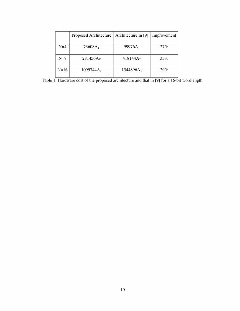
Table 1 shows the area occupied by the proposed 2D DCT architecture and the architecture in [9]
for N=4, 8 and 16. The area for each unit in both architectures is computed using the procedure
reported in [13], where AT is the area required in an inverter circuit. It is assumed that AAND=2AT,
AFA=10AT and AReg(1)=7AT. It can be seen that for N=8 about 33% reduction in the hardware cost
has been achieved by the proposed architecture over the architecture in [9].
6. Conclusions
In this paper, a new fully parallel architecture based on row-column decomposition has been
proposed for the computation of the 2D DCT. The system involves no memory transposition,
and is highly modular and utilises a highly parallel structure to achieve high-speed performance.
Due to its widely identical units, it will be relatively easy to implement and very suited to VLSI
implementation. It uses two identical units for the computation of the row and column
transforms and arrays of shift registers to perform the transposition operation. As compared to
the pipelined regular architecture in [9], the proposed architecture achieves the same throughput
rate at much lower hardware cost and communication complexities. It also requires a much
simpler control than the architecture in [9], which requires shuffling of the input data to allow a
relatively simplified architecture for the second and third stages. It is also worth mentioning that
in the proposed design, the same architecture can be used for the computation of both the
forward and the inverse 2D DCT.
17
Acknowledgement: This works is sponsored by the United Kingdom Engineering and Physical
Sciences Research Council.
References
[1]. K. R. Rao and P. Yip. Discrete Cosine Transform; Algorithms, Advantages and
Applications. Academic Press Inc., 1990.
[2]. M. Liou. Overview of the p × 64 kbits/s Video Coding Standard. Commun., ACM, vol.
34, no. 4, pp. 59 – 63, Apr. 1991.
[3]. G. K. Wallace. The JPEG Still Picture Compression Standard. Commun., ACM, vol. 34,
no. 4, pp. 30 – 40, Apr. 1991.
[4]. D. LeGall. A Video Compression Standard for Multimedia Applications. Commun.,
ACM, vol. 34, no. 4, pp. 46 – 58, Apr. 1991.
[5]. ISO/IEC DIS 13818 – 2, MPEG-2 Video. Draft Int. Standard.
[6]. S. C. Hsia, B. D. Liu, J. F. Yang and B. L. Bai. VLSI Implementation of Parallel
Coefficient-by-Coefficient Two-Dimentional IDCT Processor. IEEE Trans. on Circuits
and Systems for Video Tech., vol. 5, no. 5, pp. 396 – 406, Oct. 1995.
[7]. J. S. Chiang, Y. F. Chui and T. H. Chang. A High Throughput 2-Dimensional DCT/IDCT
Architecture for Real-Time and Video System. IEEE Proc. of Int’l Conf. on Electronic
Circuits and Systems, vol. 2, pp. 867 – 870, Sept. 2001.
[8]. P. G. Fernández et. al. Fast RNS-Based 2D-DCT Computation on Field-Programmable
Devices. IEEE Workshop on Signal Processing Systems, pp. 365 – 373, Oct. 2000.
[9]. Y. T. Chang and C. L. Wang. New Systolic Array Implementation of the 2D Discrete
Cosine Transform. IEEE Trans. on Circuits and Systems for Video Tech., vol. 5, no. 2,
Apr. 1995.
18
[10]. A. Aggoun et.al.: ‘Bit-level pipelined digit-serial array processors’ IEEE Trans. Circuit
and Systems, vol. 45, no. 7, pp. 857-868, July 1998.
[11]. R. Baugh and B. A. Wooley. ‘A Two’s Complement Parallel Array Multiplication
Algorithm’, IEEE Trans. Computers, vol. C-22, no. 12, pp. 1045 – 1047, Dec. 1973.
[12]. A. Aggoun. ‘Two’s Complement Parallel Multiplier’. Electronic Letters, vol. 34, no. 16,
pp. 1570 – 1571, Aug. 1998.
[13]. C. L. Wey and T. Y. Chang: ‘Design and analysis of VLSI based parallel multipliers’
IEE Proc. E, vol. 137, no. 4, pp. 328-336, 1990.
19
Proposed Architecture Architecture in [9] Improvement
N=4 73608AT 99976AT 27%
N=8 281456AT 418144AT 33%
N=16 1099744AT 1544896AT 29%
Table 1: Hardware cost of the proposed architecture and that in [9] for a 16-bit wordlength.
20
(a)
(b)
Figure 1: (a) Architecture of a 1D DCT Block for N=8. (b) basic cell.
.. Z22 Z21 Z20
.. Z02 Z01 Z00
.. Z42 Z41 Z40
.. Z62 Z61 Z60
.. Z12 Z11 Z10
.. Z32 Z31 Z30
.. Z52 Z51 Z50
.. Z72 Z71 Z70
VIP Processor
C21 C22 C23 C20
C01 C03 C00
C41 C42 C43 C40
C61 C62 C63 C60
C11 C12 C13 C10
C31 C32 C33 C30
C51 C52 C53 C50
C71 C72 C73 C70
C02
X11 X31 X01 X21 X61 X41 X71 X51
X10 X30 X00 X20 X60 X40 X70 X50
cpi
Sin Sout
Xij +(-1)p X(N-1-i)j
21
Figure 2: Block diagram of the 2D DCT for N=8.
3-bit Control Signal
Input Vector
1D DCT
8:1
1D DCT
Skewed Registers
Output Vector
8:1
Row Transform
Column Transform
R2
R1
22
(a) Cycle 1
(b) Cycle 2
8:1
8:1 8:1
8:1
8:1 8:1
8:1
8:1
8 words Bus
Array of skewed register R1
Z10
Z20
Z30
Z40
Z50
Z60
Z70
Z00
Array of skewed register R2
Z10 Z20 Z30 Z40 Z50 Z60 Z70
8:1
8:1 8:1
8:1
8:1 8:1
8:1
8:1
8 words Bus
Array of skewed register R1 Z00
Z11
Z21
Z31
Z41
Z51
Z61
Z71
Z01
Array of skewed register R2
23
(c) Cycle 3
(d) Cycle 4
Figure 3: Utilisation of the skewed registers during the first four cycles.
Z11 Z21 Z20 Z31 Z30 Z41 Z40 Z51 Z50 Z61 Z60 Z71 Z70
8:1
Z00
8:1 8:1
8:1
8:1 8:1
8:1
8:1
8 words Bus
Array of skewed register R1 Z10 Z01
Z12
Z22
Z32
Z42
Z52
Z62
Z72
Z02
Array of skewed register R2
Z12 Z22 Z21 Z32 Z31 Z30 Z42 Z41 Z40 Z52 Z51 Z50 Z62 Z61 Z60 Z72 Z71 Z70
8:1
Z10 Z00
8:1 8:1
Z01
8:1
8:1 8:1
8:1
8:1
8 words Bus
Array of skewed register R1
Z20 Z11 Z02
Z13
Z23
Z33
Z43
Z53
Z63
Z73
Z03
Array of skewed register R2
24
Figure 4: Utilisation of the skewed registers at the 9th cycle for N=8.
Z17
Z27 Z26
Z37 Z36 Z35
Z47 Z46 Z45 Z44
Z57 Z56 Z55 Z54 Z53
Z67 Z66 Z65 Z64 Z63 Z62
Z77 Z76 Z75 Z74 Z73 Z72 Z71 8:1
Z60
Z50
Z40
Z30
Z20
Z10
8:1 8:1
Z51
Z41
Z31
Z21
Z11
8:1
Z42
Z32
Z22
Z12
Z02
8:1 8:1
Z15
8:1
Z33
Z23
Z13
Z03
8:1
Z24
Z14
Z04
8 words Bus
Array of skewed register R1 Z70 Z61 Z52 Z16 Z25 Z43 Z24
Z10
Z20
Z30
Z40
Z50
Z60
Z70
Z00
Z00
Z01
Z06
Z05
Z07
Array of skewed register R2
25
Figure 5: Dependency graph of the proposed radix-2n VIP
uK-1,N/2 VN/2
V2
V1 u01 u11 uK-1,1
u02 u12 uK-1,2
u0,N/2 u1N/2
Partial product generation path
Partial sums path
26
Figure 6: Array multiplier used for each of the partial product generation uri Vi for B=16.
AFA
HA
HA
AFA
AFA
AFA
0riu
1riu
2riu
3riu
0iv1
iv2iv14
iv15iv
���
≠=
0001
rif
rif
AND gate if r = 3 NAND gate if r ≠ 3
AND gated FA if r = 3 NAND gated FA if r ≠ 3
Sum Word
Carry Word
27
4B 4
B 4B 4
B 4B 4
B 4B
k=3 k=2 k=1 k=0 k=7 k=6 k=5 k=4
14B −
1 1 1 1 1
Figure 7: Repartitioning of the partial sum and carry words into B/4-bits and their relative bit
positions for N=8.

28
Partial Product generation
(2B+4)-bit result
Carry LookAhead Adder
k=7 k=6 k=5 k=4 k=3 k=2 k=1
0100
P Q
k=0
32-2 28-2 20-2 12-2 8-2 16-2 24-2 4-2
Figure 8: Accumulation process of the partial products for N=8
Figure 9: Partial products accumulation for N=8 and k=4 using a 32-2 compressor.
Outputs to be fed to the CLA
32 Partial products for k=4
B/4-bit 4-2 Compressor
29
Figure 10: Partial products accumulation for N=8 and k=5 using a 24-2 compressor.
24 Partial products for k=5
Carry bits from previous array of 4-2
compressors
Outputs to be fed to the CLA
B/4-bit 4-2 Compressor
1-bit 4-2 Compressor
Related Documents