SERVICE MANUAL Colour Television Specifications Power Source . . . . . . . . AC220-240V, 50/60Hz. Colour System . . . . . . . PAL, SECAM, NTSC4.43, NTSC Television System . . . . . B/G Channel Coverage . . . .VHF: 0-11, 5A (Australia), 1-11 (New Zealand) UHF: 28-69 (Australia), 21-69 (New Zealand) CATV: S1-S41, X, Y, Z, Z+1, Z+2 Aerial Input Impedance 75Ω Ext. Terminals AV1 (Rear): CENELEC Standard Input (Composite video, RGB and audio-L/R) Output (TV-output with composite video and audio-L/R) AV2 (Rear): Phone jac k ( Video input and Audio-L/R input) S-Video Input (Din 4 pin, Separated Y/C signals input) AV3 (Front): Phone jac k ( Video input and Audio-L/R input) Monitor Output: Phone jac k (Video monitor output and Audio-L/R monitor output) Headphone Jack: Mini Stereo Jack Speaker . . . . . . . . . . 5 cm ✕ 12 cm ✕ 2 pcs. Sound Output . . . . . 5W + 5W Dimensions . . . . . . . . . . 774 (W) ✕ 491 (H) ✕ 508 (D)mm Weight . . . . . . . . . . . . . . . approx. 36.9 Kg Specifications subject to change without notice Original Version Chassis Series: FAW-1 F8WA FILE NO. Model No. CP28WF2 Service Ref. No. CP28WF2-00 (Australia/New Zealand) Give complete “SERVICE REF. NO.” for parts order or servicing. It is shown on the rating plate at the cabinet back of the unit. This T.V. receiver will not work properly in foreign countries where the television transmission system and power source dif- fer from the design specifications. Refer to the specification table. Product Code:111371200 REFERENCE NO. SM5110615 TV/AV MENU CH

Welcome message from author
This document is posted to help you gain knowledge. Please leave a comment to let me know what you think about it! Share it to your friends and learn new things together.
Transcript

SERVICE MANUAL Colour Television
SpecificationsPower Source . . . . . . . .AC220-240V, 50/60Hz.Colour System . . . . . . .PAL, SECAM, NTSC4.43, NTSCTelevision System . . . . .B/GChannel Coverage . . . .VHF: 0-11, 5A (Australia), 1-11 (New Zealand)
UHF: 28-69 (Australia), 21-69 (New Zealand)CATV: S1-S41, X, Y, Z, Z+1, Z+2
Aerial Input Impedance 75ΩExt. Terminals
AV1 (Rear): CENELEC StandardInput (Composite video, RGB and audio-L/R)Output (TV-output with composite video and audio-L/R)
AV2 (Rear): Phone jack (Video input and Audio-L/R input)S-Video Input (Din 4 pin, Separated Y/C signals input)
AV3 (Front): Phone jack (Video input and Audio-L/R input)Monitor Output: Phone jack (Video monitor output and Audio-L/R monitor
output)Headphone Jack: Mini Stereo Jack
Speaker . . . . . . . . . . 5 cm 12 cm 2 pcs.Sound Output . . . . . 5W + 5WDimensions . . . . . . . . . . 774 (W) 491 (H) 508 (D)mmWeight . . . . . . . . . . . . . . .approx. 36.9 Kg
Specifications subject to change without notice
Original Version
Chassis Series: FAW-1
F8WA
FILE NO.
Model No. CP28WF2
Service Ref. No. CP28WF2-00
(Australia/New Zealand)
Give complete “SERVICE REF. NO.” for partsorder or servicing. It is shown on the rating plateat the cabinet back of the unit.
This T.V. receiver will not work properly inforeign countries where the televisiontransmission system and power source dif-fer from the design specifications. Refer tothe specification table.
Product Code:111371200
REFERENCE NO. SM5110615
TV/AV MENUCH

Contents
-2-
Safety Notice . . . . . . . . . . . . . . . . . . . . . . . . . . . . . . . . . . . . . . . . . . . . . 2Chassis Block Diagram . . . . . . . . . . . . . . . . . . . . . . . . . . . . . . . . . . . . . 3IC Block Diagrams . . . . . . . . . . . . . . . . . . . . . . . . . . . . . . . . . . . . . . . 4-6CPU Port Functions . . . . . . . . . . . . . . . . . . . . . . . . . . . . . . . . . . . . . . . . 7Option Setting . . . . . . . . . . . . . . . . . . . . . . . . . . . . . . . . . . . . . . . . . . . . 8Service Adjustments . . . . . . . . . . . . . . . . . . . . . . . . . . . . . . . . . . . . . 9-12Purity and Convergence Adjustment . . . . . . . . . . . . . . . . . . . . . . . . 13-14Mechanical Disassembly . . . . . . . . . . . . . . . . . . . . . . . . . . . . . . . . . . . 15Protection Circuit . . . . . . . . . . . . . . . . . . . . . . . . . . . . . . . . . . . . . . . . . 15Cabinet Parts List . . . . . . . . . . . . . . . . . . . . . . . . . . . . . . . . . . . . . . . . 16Chassis Electrical Parts List . . . . . . . . . . . . . . . . . . . . . . . . . . . . . . . 17-27Component Locations . . . . . . . . . . . . . . . . . . . . . . . . . . . . . . . . . . . 28-29Voltages and Waveforms Charts . . . . . . . . . . . . . . . . . . . . . . . . . . . 30-31
Safety Notice
SAFETY PRECAUTIONS
1: An isolation transformer should be connected in thepower line between the receiver and the AC linewhen a service is performed on the primary of theconverter transformer of the set.
2: Comply with all caution and safety-related notes pro-vided on the cabinet back, inside the cabinet, on thechassis or the picture tube.
3: When replacing a chassis in the cabinet, always becertain that all the protective devices are installedproperly, such as, control knobs, adjustment coversor shields, barriers, isolation resistor-capacitor net-works etc.. Before returning any television to thecustomer, the service technician must be sure thatit is completely safe to operate without danger ofelectrical shock.
X-RADIATION PRECAUTION
The primary source of X-RADIATION in television receiver is the picture tube. The picture tube is specially con-structed to limit X-RADIATION emissions. For continued X-RADIATION protection, the replacement tube must bethe same type as the original including suffix letter. Excessive high voltage may produce potentially hazardous X- RADIATION. To avoid such hazards, the high voltage must be maintained within specified limit. Refer to this ser-vice manual, high voltage adjustment for specific high voltage limit. If high voltage exceeds specified limits, takenecessary corrective action. Carefully follow the instructions for + B1 volt power supply adjustment, and high volt-age check to maintain the high voltage within the specified limits.
PRODUCT SAFETY NOTICE
Product safety should be considered when a component replacement is made in any area of a receiver.Components indicated by mark in the parts list and the schematic diagram designate components in whichsafety can be of special significance. It is particularly recommended that only parts designated on the parts listin this manual be used for component replacement designated by mark . No deviations from resistancewattage or voltage ratings may be made for replacement items designated by mark .

Q61
1
IC34
51N
ICA
M/S
TE
RE
O D
EC
OD
ER
78 55565758616875767980
71
53
39
4733232221202726
141312
IC80
1C
PU
1
4
33,3
4
53
54
112120198
17 16 1518
45
IC20
1IF
/VID
EO
/C
HR
OM
A/
DE
F.
BLK
R IN
G IN
B IN
33,3
447
,48
36,3
7
31,3
24
51,5
212
5
60,6
1
IC00
1A
UD
IO A
MP.
8,10
1,5
3
AU
DIO
L &
R
HE
AP
HO
NE
JA
CK
& S
WIT
CH
SP
EA
KE
RS
P90
1S
P90
2
A10
1F
/S T
UN
ER
AE
RIA
L
SC
LS
DA
RF
AG
C
19 151,32,6
20 11 7
K1001 AV1 SCART
VID
EO
OU
T
VID
EO
OU
T (
TV
)
CR
T
FO
CU
S/S
CR
EE
N
R BG
Y IN
C IN
K10
04 A
V2
S-V
IDE
O
V L R
K1101AV3 IN (FRONT)
V L R
K1003 MONITOR OUT
V L R
K1002 AV2 IN
VIF
IN
VIF
INS
AW
FIL
TE
R(V
IF)
X13
2
SIF
IN
SIF
INS
AW
FIL
TE
R(S
IF)
X13
1
IC12
01V
IDE
O S
W
8
9
64
1
AV
1 V
IDE
O IN
AV
1
VID
EO
/Y S
WIC
1050
AV
1 A
UD
IO IN
AV
2 A
UD
IO IN
AV
1 A
UD
IO IN
AV
2 A
UD
IO IN
AV
1 A
UD
IO O
UT
AV
2 V
IDE
O IN
1A
V2
(VID
EO
or Y
IN)
7
3
AV
3 (V
IDE
O IN
)
AV
3 A
UD
IO IN
R IN
G IN
B IN
R IN
G IN
B IN
C IN
VID
EO
/Y O
UT
VID
EO
/Y IN
VID
EO
MO
NIT
OR
O
UT
AU
DIO
MO
NIT
OR
OU
T
AU
DIO
MO
NIT
OR
OU
T(L
& R
)
(Fro
m p
in-4
7 &
48
of IC
3451
)
VID
EO
MO
NIT
OR
OU
T
R O
UT
G O
UT
B O
UT
SC
L
SD
ASIF
OU
T
SC
LS
DA
16M
UT
E
RC
R
EC
EIV
ER
A19
01
KE
Y S
W
ME
MO
RY
IC80
3S
CL
SD
A
IIC B
US
C
ON
TR
OL
SW
691
T61
1C
ON
VE
RT
ER
TR
AN
S.
L902
DY
15
85 32
AC
PLU
G
D60
3-D
606
C60
7
Q61
3
5VQ
666
Q66
1
PR
OT
EC
T
IC64
35V
-1
IC64
29V
IC64
15V
D64
6
D64
1
D64
7
27V
18 11 14 101213
D63
7
27V
Q65
1
150V
Q64
2Q
641 Reg
.
-27V
Q64
3
Q68
6
Q68
2
D61
5
PH
OTO
CO
UP
LER
Q64
5
Q68
5
PO
WE
R
EW
-OU
T
V-O
UT
H-OUT
T45
1F
BT
HV
200V
Q43
2H
-OU
T
Q43
1IC
501
VE
RT.
DE
F.
36
H-B
LAN
K
Q46
2D
441
Q46
1
L461
L462
SCREEN WIDTH CONTROL
CR
TH
EAT
ER
-3-
Chassis Block Diagrams

IC201 < IF/Video/Chroma/Def.> TB1262F
-4-
IC Block Diagrams
Cync. out
H.AFC H,V
Syn
c.A
FC
1/H
AF
C g
ain
V fr
eqw
ide
blan
king
DC Resistor
BLACK DET
YS(YCbCr)
Cb2/B IN
Cbr2/R IN
Y2/CVBS2/G IN
Cb3 IN
Cb3 IN
Y3/CVBS3 IN
Cr OUT
Cb OUT
Y/MON OUT
Y/CVBS1 IN
C IN
IF DET OUT
DAC 1
DAC 3
DAC 2
Loop
Filt
er
VIF
VC
O F
SIF
OU
T
HV
cc (
9V)
SIF
IN
IF GND
DC
NF
SIF IN
N.C.
VIF IN
VIF IN
S-Filter
APC Filter
X' tal
CW OUT
R OUT
G OUT
B OUT
VM OUT
EXT. R IN
EXT. G IN
EXT. B IN
Y sm
ABCL IN
SDA
SCL
Bed pin
45 35 50 41 40 39 37 33 28 47 46 11 25 17
42
23
20
31
27
26
32
4746778169371737065
68
58
61
53
52
51
55
57
56
59
54
62
43
66
36
19
44
49
48
12
13
14
18
21
22
79
80
9
7
6
34
72
75
76
77
Dig
. VD
D
Dig
. GN
D
RG
B V
cc (
9V)
YC
Vcc
(5V
)
V R
AM
P
V O
UT
EH
T IN
EW
OU
T
FB
T IN
H O
UT
VD
HD
SC
P O
UT
YC
GN
D
H D
RIV
EA
FC
2P
alaG
Baw
IIC B
us
IF
-EW
-C
oner
(T/B
)S
ize
Trap
eze
Par
abol
aV/E
W-E
W-
Siz
eV
Cen
tre
V L
inea
rV
-S
SIF IN
FM
Filt
er
IF V
cc(9
V)
RF
AG
C
IF A
GC
IF V
cc(5
V)
SA
WS
AW
-1 s
t S
IF-
QS
S d
emp
AM
dem
oVIF
/SIF
-VIF
-V
CO
S-T
rap
AF
T (
to B
us)
neg/
pos
SIF
BP
FF
M(A
M)
RG
B--
>Y
UV
Y1
Pro
c.C
-Tra
pY
Del
ay
Ch
rom
aPA
L/N
TS
C/
SE
CA
M
YU
V S
wit
ch
UV
Pro
c.B
BT
INT
Col
our
Con
tras
t
Y2
Pro
c.B
lack
str
etch
DC
res
isto
rW
PL/
A.C
./W
PS
RG
B P
roc.
YU
V->
RG
B/S
WC
ut o
ff/D
rive
Y/C
YCbCr2
YCbCr3

IC Block Diagrams
-5-
IC001 < Audio AMP.> TA8200AH
1
2
3MUTE
REFERENCES
NON INVERTING INPUT (1)
INVERTING INPUT (1)
SUR/MUTING
TURN ON AND OFF
9
5
10
84
6
Vcc
NON INVERTING INPUT (2)
INVERTING INPUT (2)
L
R
-
+
-
+
GND
RF I 27K
RF I 27K
SCPROTECTION
Tj
THPROTECTION
OUTPUT-L
OUTPUT-R
TDA7263M
IC501 < Vertical Output > LA7846N
THERMALPROTECTION
PUMPUP
AMP
-
+
N.C
.
Ver
. Out
put
Out
put
Sta
ge V
cc
Non
Inv.
Inpu
t
Inve
rtin
gIn
put V
cc
Pum
p U
pO
utpu
t
LA7846N
1 3 4 5 6 7 8 9 10
GN
D
2
N.C
.
N.C
.

-6-
IC Block DiagramsIC3451 < Digital TV Sound Processor > TDA9875A
I2C-BUSINTERFACE
ADDR1ADDR2
P1P2
920
SCLSDA
31345
IDENTIFICATION
CLOCKXTALI
XTALOSYSCLK
181721
PEAKDETECTION
SDI1SDI2
SDO1SDO2
SCKWS
272625242223
I2C-BUSAUDIO
INTERFACE
VDDD1VDDD2VSSD1VSSD2
CRESET
1564144916
DIGITALSUPPLY
TEST1TEST2
2830 TEST
TDA9875
MOL MOR AUXOL AUXOR
61 60 58 57
SUPPLYOPERATIONALAMPLIFIERS
DAC(2) DAC(2)
AUDIO PROCESSING
DAC(2)
ADC(2)
DIGITALSELECT
LEVELADJUST
LEVELADJUST
DEMATRIX NICAMDECODER
FM (AM)DEMODULATION
NICAMDEMODULATION
INPUT SWITCHAGC, ADC
SIF2 SIF1
10 12
SUPPLYSOUND IF
(SIF)
VDDA1VSSA1Vref1Iref
TIMINGDETECTION DAC
19
21
Vtune
NICAMPCLK
SCIR1SCIL1SCIR2SCIL2EXTIREXTILMONOIN
33343637313229
SCOR1SCOL1SCOR2SCOL2LORLOL
474851526362
ANALOGCROSSBAR
SWITCH
CAPL2CAPL1
CAPR1CAPR2
4241
4544
PCAPRPCAPL
VDDA2VSSA2VSSGVref2
Vref(P)
Vref(n)
5455
384335463940
SUPPLYDAC
VDDA3VSSA3
Vref3
VSSA4
SUPPLY DAC
REFERENCE
5956
53
50
76
118
(first general purpose I/O pin)
(second general purpose I/O pin)(first I2C-bus slave address modifier)
(second I2C-bus slave address modifier)
(I2C-bus clock)
(I2C-bus data)
(crystal oscillator input)(crystal oscillator output)(system clock output)
(I2S-bus data input 1) (I2S-bus data input 2)
(I2S-bus data output 1) (I2S-bus data output 2)
(I2S-bus clock) (I2S-bus word select)
(digital supply voltage 1)
(digital supply voltage 2)
(supply ground 1)(supply ground 2)
(capacitor for power-on reset)
(first test pin)(second test pin)
(analog supply voltage 1)
(supply ground 1)(reference voltage)
(resistor for reference current generator)
(tuning voltage output for crystal oscillator)
(serial NICAM data output at 728 kHz)
(NICAM clock output at 728 kHz)
(SCART 1 input right channel) (SCART 1 input left channel)
(SCART 2 input right channel)
(SCART 2 input left channel)
(external audio input right channel) (external audio input left channel)
(audio mono input)
(SCART 1 output right channel)
(SCART 1 output left channel)
(SCART 2 output right channel)
(SCART 2 output left channel) (line output right channel)(line output left channel)
(filter capacitor pin 2 )(filter capacitor pin 1)
(filter capacitor pin 1)(filter capacitor pin 2)
(post-filter capacitor pin right channel, audio digital-to-analog coverter)
(post-filter capacitor pin left channel, audio digital-to-analog converter) (analog supply votage 2)(supply ground 2)
(ground guards)(reference voltage)(positive reference voltage)(reference voltage ground)
(analog supply voltage)
(supply ground 3)
(reference voltage)
(supply ground 4)
(Lou
dspe
aker
(M
ain)
ou
tput
rig
ht c
hann
el)
(Lou
dspe
aker
(M
ain)
ou
tput
left
chan
nel)
(Hea
dpho
ne (
Aux
iliar
y)
outp
ut r
ight
cha
nnel
)
(Hea
dpho
ne (
Aux
iliar
y)
outp
ut le
ft ch
anne
l)
(sou
nd IF
in
put 2
)
(sou
nd IF
in
put 1
)

-7-
CPU Port Functions
Pin No. Function Name Function IN/OUT
1 RC IN RC signal input IN
2 RESET Reset input IN
3 50/60 50/60Hz output (50Hz=H) OUT
4 H-BLK H-Blank OUT
5 V-BLK V-Blank OUT
6 AV SW2 Option SW2 OUT
7 AV SW1 Option SW1 OUT
8 KEY IN Key switch signal input IN
9 H-P Headphone mute (not used) OUT
10 RELAY To operate degauss circuit OUT
11 PROTECT Power failure detect IN
12 HP-mode Headphone mute OUT
13 BBE BBE ON/OFF OUT
14 W-P White enable OUT
15 B-OUT Blue output OUT
16 G-OUT Green output OUT
17 R-OUT Red output OUT
18 FB-OUT Fast blanking output OUT
19 SDA SDA IN/OUT
20 SCL SCL OUT
21 VDD VDD --
22 JDTO Not used --
23 N.C. Not used --
24 Vpp Not used --
25 AVDD3 Analog VDD of PLL --
26 TEST0 Test pin --
27 MCFM Test pin --
28 JTCK Test pin --
29 TXCF Analog pin for the --Teletext slicerline PLL
30 CVBSO Not used --
31 AVDD2 Analog power supplies --
32 JTMS Not used --
33 CVBS2 Video input (H.F) IN
34 CVBS1 Video input (L.F) IN
35 AGND Analog circuit ground --
36 GND Digital circuit ground --
37 JTRSTO Test pin --
38 PXFM Analog pin for the Display --Pixel Frequency Multiplier
39 AVDD Analog power supplies --
40 H-SYNC Horizontal Sync input IN
41 V-SYNC Vertical Sync input IN
42 ACK Answer for status OUT
43 STATUS Request for Bus open IN
44 IGNOA RGB on/off switch OUT
45 AMP-MUTE Sound mute on/off switch OUT
46 L/L’ L/L’ switch OUT
Pin No. Function Name Function IN/OUT
47 LED2 Brightness control of LED OUT
48 S-VIDEO SW S-video switch OUT
49 H-Phase H-Phase (not used) OUT
50 OSC OUT Oscillator (output) OUT
51 OSC IN Oscillator (input) IN
52 RF AGC RF Auto gain control IN
53 PITTARI PITTARI switch OUT
54 POWER TV power on/off switch OUT
55 8PIN (SC2) AV input detect IN
56 8PIN (SC1) AV input detect IN

Option Setting
-8-
After replacing the Memory IC (IC803)The memory IC (IC803), stores the option data of TV set and service adjustments data for each circuit, therefore, whenthe memory IC is replaced, it should be programmed to the following settings and “ SERVICE ADJUSTMENT” onpages 9 to 12.
1) To enter to the Option ModePress and hold the F/OK button on the remote control and Programme down button (CH) on the front panel of the TV. The option window will appear on the screen.
TV/AV MENU CH
ON-TIMERSORT MODEP&PWel. TextComb FilterWSS-AustAuto Volume3D SurroundCountryAV3CS/A,B
ONTuningONONOFFONOFFONBG/DK/I/LL'ONCS
Option Mode
2) To set the Option ModeSelect the desired option item by pressing the Programme down or up button.To switch the option mode, use the Level up or down button.The data which is set in the option mode is stored into the memory IC automatically.
The following table shows the available option items and default setting mode.
Option Mode Mode Description & NoteON-TIMER ON or OFF On-timer available, default “ON”SORT MODE Sorting or Tuning Tuning mode, default “TUNING”P & P ON or OFF Plug & Play mode, default “ON”WEL. TEXT ON or OFF Display message when first set up, default “ON”Comb Filter OFF or ON For factory use, default “OFF”WSS-Aust ON or OFF Default “ON”Auto Volume ON or OFF Auto volume, default “OFF”3D Surround ON or OFF Default “ON”Country UK or IRE or B/G, D/K, I, L/L’ TV system, default “ B/G, D/K, I, L/L ”Wide ON or OFF Wide mode, default “ON”AV3 ON or OFF Front AV disable, default “ON”CS/A,B CS or A/B Default “CS”
3) Exit from the Service ModePress the Programme information call button or turn off the TV set by using the mains switch.

Service Adjustments
-9-
After replacing the Memory IC (IC803)The memory IC (IC803), stores the service adjustment data for each circuit, therefore, when the memory IC isreplaced, it should be programmed by using “OPTION SETTING” on previous page and the following adjustment.
Adjustable Service Adjustment
Regular
Item No. OSD Description01 AGC AGC Adjustment02 -- Cut-Off Drive Adjustment03 GRY G-Drive Adjustment (White Balance)04 GRY B-Drive Adjustment (White Balance)05 CTR Contrast Adjustment (use factory setting) (for factory use)06 -- Screen Adjustment mode08 OSD OSD Positioning Adjustment
Note: Some items of the service adjustments for this chassis are controlled by the CPU (IC801), and the adjustments are carried out by using the RC handset.
Image
Item No. OSD Description01 P V-C P Vertical Position Adjustment02 P H-P P Horizontal Position Adjustment03 P V-L P Vertical Linearity Adjustment04 P VSC P Vertical S-Correction Adjustment05 P V-A P Vertical Size Adjustment06 P H-S P Horizontal Size Adjustment07 P E-P P Pin Cushion Adjustment08 P E-T P Trapezoid Distortion Adjustment11 P ECT P Top Corner Correction Adjustment12 P ECB P Bottom Corner Correction Adjustment13 P HPA P Parallelogram Distortion Adjustment
Important Notice:Do not attempt to adjust service adjustments not listed on above otherwise it may cause loss of performance andproduct safety.

Service Adjustments
-10-
1) To enter to the Service ModePress and hold the GREEN button on the remote control and then press the Programme down button (CH) on the front panel of the TV.Press the Programme down button to select the mode required (Regular, Image, others and TB12**). Then press the F/OK button to select the mode.
The available adjustment items are as follows;Image :This can be adjusted for picture image/Shapes.Regular :This can be adjusted for the service adjustment.Other :This is for the factory setting. DO NOT ADJUST.TB1251 :This is for the factory setting. DO NOT ADJUST.
2) To select the mode and service item and change data valueSelect the desired adjustment mode by pressing the Programme down or up button and press the F/OK button.To select the adjustment item, use the Programme down or up button.To change the service data, use the Level up or down button.The data which is set in the service mode is stored into the memory IC automatically.
Regular01 AGC 38
Image01 P V-P 24
REGULAR mode IMAGE mode
3) Exit from the Service ModePress the Programme information call button or turn off the TV set by using the mains switch.
Initialisation of Memory IC (IC803)To initialise the memory IC (IC803), press and hold the Picture mode selection (→•←) button on the remote control, then press the Programme down button on the front panel of the TV set and then turn the Mains switch off and on. The initialisation is now completed.When initialised the memory IC and all of the setting data (option data and service adjustment data) stored in the ICare reset to the default value. It is necessary to set the option settings and readjust the service adjustments listed on page 9 and to re-tune all the channels.
Adjustment DataAdjustment No.and Item name
Adjustment DataAdjustment No.and Item name

Adjustments
-11-
IMPORTANT NOTICEDo not attempt to adjust the following service adjustments except when adjustments are required in servicing other-wise it may cause loss of performance and product safety.
+B VOLTAGE ADJUSTMENT
(1) Connect a DC voltmetre to TP-B and the ground.(2) Tune the receiver to an active channel and synchronized pic-
ture. Select NATURAL picture mode by pressing the Picturemode selection button on the remote control .
(3) Adjust voltage to 150± 0.5V DC by using VR641.
AGC ADJUSTMENT
NOTE: Do not attempt this adjustment with weak signal.(1) connect digital voltmetre to TP-A and GND.(2) Tune the receiver to most clearest (or strongest) VHF station
in your area. Set the brightness and contrast controls to max-imum. Set the colour control to minimum.
(3) Enter to the service mode and select mode “Regular”, andselect item No. 01 “Regular 01 AGC”
(4) Press the Level up (+) or Level down (-) button to adjustvoltage to be 3.2± 0.2V DC.
FOCUS ADJUSTMENT
(1) Receive a monochrome circular pattern.(2) Set the brightness to normal and contrast to maximum.(3) By using FOCUS VR on the F.B.T., adjust focus control for
well defined canning lines.
SCREEN ADJUSTMENT(1) Receive black & white pattern.(2) Set the brightness and colour to normal, contrast to maxi-
mum.(3) Enter to the service mode and select mode “Regular”, then
select item No. 02 “Regular 02 CUT”. The horizontal line willappear on the screen.
(4) Using the numeric buttons shown set each colour to minimumby decreasing to the point where any further decrease resetsthe adjustment to maximum value.
BIAS ADJUSTMENT(5) By using the buttons 1, 2, 3, 4, 5, 7, 8 on the remote control,
adjust the line to be white.
The key allocation is as follows;Button No. Operation
1 Increase Red2 Decrease Red4 Increase Green5 Decrease Green7 Increase Blue8 Decrease Blue
GREY SCALE ADJUSTMENT
DRIVE ADJUSTMENT(6) Select item No. 3. “Regular 03 GRY” (G-Drive) or No.04
“Regular 04 GRY” (B-Drive) and adjust both initially to 40.(7) Change data value of each item by using Level up(+) or Level
down(-) button to obtain the proper white balance.
PCC ADJUSTMENT
PCC ADJUSTMENT(1) Receive cross hatch pattern and set screen mode to “FULL”.(2) Enter to the service mode and select mode “Image”, and
select item No. 07 “Image 07 P E-P”.(3) Press the Level up (+) or Level down (-) button to adjust the
vertical line to be straight.
TRAPEZOID ADJUSTMENT(1) Receive cross hatch pattern and set screen mode to
“FULL”.(2) Enter to the service mode and select mode “Image”, and
select item No. 08 “Image 08 P E-T”.(3) Press the Level up (+) or Level down (-) button to correct
the trapezium distortion of the vertical line.
CORNER ADJUSTMENT(1) Receive cross hatch pattern and set screen mode to
“FULL”.(2) Enter to the service mode and select mode “Image”, and
select item No.11 “Image 11 P ECT” for top corner adjustmentor item No. 12 . “Image 12 P ECB” for bottom corner adjust-ment.
(3) Press the Level up (+) or Level down (-) button to correctthe distortion of the vertical line around the corners..

Adjustments
-12-
HORIZONTAL ADJUSTMENT
HIGH-VOLTAGE CONFIRMATION
VERTICAL ADJUSTMENT
HORIZONTAL CENTRING ADJUSTMENT(1) Receive circular pattern and set screen mode to “FULL”.(2) Enter to the service mode and select mode “Image”, and
select item No. 02 “Image 02 P H-P”.(3) Press the Level up (+) or Level down (-) button to adjust the
horizontal centre.
VERTICAL CENTRING ADJUSTMENT(1) Receive circular pattern and set screen mode to “FULL”.(2) Enter to the service mode and select mode “Image”, and
select item No. 01 “Image 01 P V-C”.(3) Press the Level up (+) or Level down (-) button to adjust the
vertical centre.
Horizontal centre
HORIZONTAL WIDTH ADJUSTMENT(1) Receive circular pattern and set screen mode to “FULL”.(2) Enter to the service mode and select mode “Image”, and
select item No. 06 “Image 06 P H-S”.(3) Press the Level up (+) or Level down (-) button to adjust the
horizontal width.
Note: +B (+150V) Voltage Check and Grayscale Adjustment mustbe completed before attempting High Voltage Check.
(1) Connect high-voltage meter to the anode of CRT and theground.
(2) Receive circular pattern and set screen mode to “FULL”.(3) Set controls for brightness and contrast to maximum.(4) Confirm high voltage is within 28.5 KV and 30.5 KV at maxi
mum beam current.
VERTICAL HEIGHT ADJUSTMENT(1) Receive circular pattern and set screen mode to “FULL”.(2) Enter to the service mode and select mode “Image”, and
select item No. 05 “Image 05 P V-A”.(3) Press the Level up (+) or Level down (-) button to adjust the
vertical height.
OSA POSITIONING ADJUSTMENT
(1) Receive circular pattern and set screen mode to “FULL”.(2) Enter to the service mode and select mode “Regular”, and
select item No. 08 “Regular 08 OSD”. The OSD test bar willappear on the top of screen.
(3) Press the Level up (+) or Level down (-) button to adjustproper OSD positioning.

-13-
Signals: Use a pattern generator which can output red, green, blue and white raster and crosshatch pattern signals.
Procedure: Carry out purity adjustment first, and then carryout convergence adjustment.
Preparation: The deflection yoke may have several correction magnets attached to its outer edge. If replacing the picture tube, the positions of the magnets can be changed andthey can be re-used, so remove these magnets and keep them safely so that they do not get lost.
PURITY ADJUSTMENTS1. Place the picture so that its front faces west.2. Insert the power plug into a wall outlet, and then turn on
the power for the TV and de-magnetize the TV using itsown degaussing circuit.
3. Loosen the screw which is holding the deflection yoke(with integrated purity magnets), and them move thedeflection yoke forward as far as it will go. Remove therubber wedge at this time.
4. Turn off the red and blue raster so that only the greenraster is on.
5. Adjust the angle between the tabs (wings) on puritymagnets to centre the vertical green belt in the picturetube screen. (See Figures 2 and 3.)
NOTE: This adjustment can only be carried out by changing the angle, not by rotating the tabs up anddown.
6. Gently move the deflection yoke back to the positionwhere the green band fills the whole of the picture tubescreen, and then tighten the screw to secure the deflection yoke in place.
7. If there is any colour distortion around the edges, correctit by attaching magnets to the outer edge of the deflection yoke. The magnets should be attached sothat the line running from the position of the distortion tothe centre of the picture tube intersects the deflectionyoke.The colours on the magnets indicate the north andsouth poles of the magnets. Attach the magnets inwhichever direction causes the distortion to disappear.(See Figures 1 and 4. The south and northpole positions are shown as a guide.)
8. Switch the screen to red and blue raster and check thatthere is no colour distortion. If there is any distortion,adjust the angles of purity magnets tabs or the forward-back position of the deflection yoke, or change the attachment positions of the correction magnets.
Purity and Convergence AdjustmentCAUTION: The Convergence and Purity adjustments have been made at the factory. Readjustmentshould be made only after picture tube or deflection yoke replacement, following the steps below:
Deflection yokemounting scrrew
Rubber wedge
Correction magnet
Move the deflection yoke back and forth to adjust the purity
GREEN band
Magnet attachment position
Deflection Yoke outer edge
Color distortion
Figure 1
Figure 2
Figure 3
Figure 4
N
S
12 3 4
SIX-POLEMAGNET TABS
FOUR-POLEMAGNET TABS
ANGLEOF TABS
PURITYMAGNETTABS
Change the angle to adjust the green band so that it iscentred in the screen.

-14-
Purity and Convergence AdjustmentCONVERGENCE ADJUSTMENTPreparation: After carrying out purity adjustment and
before proceeding to convergence adjustment, provisionally insert the rubber wedge so that there is no vertical or sideways play in the deflection yoke.
Signals: Display a crosshatch pattern.
1. Red/blue centre adjustmentAdjust the angle between the tabs (1) and (2) in Figure5 and rotate them together until the lines of the red andblue crosshatch patterns (vertical and horizontal lines)are superimposed in the centre of the screen.
2. Green and red/blue centre adjustmentAdjust the angle between the tabs (3) and (4) in Figure5 and rotate them together until the lines of the greencrosshatch pattern are superimposed with the red/bluecrosshatch pattern (vertical and horizontal lines) whichwere superimposed in step 1).
3. Vertical lines at screen centre (Red and Blue)Use the VR2 control (see Figure 8) at the top of thedeflection yoke to correct the vertical line convergenceat the centre of the screen.(See Figure 9.)
4. Vertical lines at screen top and bottomUse the VR1 control (see Figure 8) at the top of thedeflection yoke to correct the vertical line convergenceat the top and bottom of the screen. (See Figure 10.)
5. Horizontal lines at screen top and bottomRotate the Deflection yoke to the left or right to correctthe horizontal line convergence at the top and bottom ofthe screen. (See Figure 11.)If vertical lines are intersecting at the top and bottom,use a screwdriver to adjust the Balance coil at the top ofthe deflection yoke. (See Figure 12.)
Red
Blue
Figure 6
Red/Blue
Green
Figure 7
Red Blue
Figure 9
Figure 5
Adjust the angle rotation of tabs(1) and (2) to align the verticaland horizontal lines.
Adjust the angle and rotation oftabs (3) and (4) to align the verticaland horizontal lines.
Use the VR2 control to correct.
RedBlu
e
Figure 10
Use the VR1 control to correct.
BlueRed
Figure 11
Rotate the DY to correct.
BlueRed
Figure 12
Use the Balance coil to correct
12 3 4
SIX-POLEMAGNET TABS
FOUR-POLEMAGNET TABS
ANGLEOF TABS
PURITYMAGNETTABS
Balancecoil
VR1
VR2
Figure 8

-15-
AV1 IN
ANT. 75Ω
L
R
AUDIO
VIDEO
(MONO)
S-VIDEO
MONITOROUT
AV2 IN
Mechanical Disassembly
CABINET BACK REMOVAL1. Refer to Figure 1, remove 14 screws.2. Pull off cabinet back and remove.
Figure 1. Cabinet Back Removal
When an abnormality occurs during TV reception, it causes pin 11 of the CPU to go continually Low (less than2.0V) for about 2 second. The CPU detects that this has occurred and outputs the signal from pin 54 to switch offthe power supply lines.
Releasing the protective circuit and restoring power supply
To release the protective circuit and restore power supply, turn the power to the TV set OFF and then ON again viaeither the main power switch or the ON-OFF button on the remote control. This will work only if the power supplytrouble was temporary. If there is permanent trouble such as a damaged circuit, power cannot be restored and thecircuit will have to be repaired.
This TV set has a built-in power supply protection circuit.It is provided to protect the TV set in case of a power supply circuit malfunctions. When something abnormality occursduring TV reception, the TV set goes to the stand-by mode.
Protection Circuit

TV/AV MENUCH
-16-
Note: Parts order must contain Service Ref. No., Part No., and descriptions.
1 610 312 8320 ASSY,BUTTON POWER-F8WA610 229 8406 SPRING-E3HA
(for POWER BUTTON)2 610 291 6775 DEC IND-S6DK3 610 312 8313 ASSY,BUTTON UNIT-F8WA4 610 312 8405 ASSY,CABINET FRONT-F8WA4-a 610 312 8436 CABINET FRONT-F8WA4-b 610 312 8467 DOOR-F8WA
5 610 312 8474 DEC SHEET DOOR-F8WA6 610 284 7741 DOOR COVER-C2SA 7 645 040 4672 BADGE,SANYOor 645 041 7269 BADGE,SANYO
8 610 291 6836 SPRING PLATE-S6DK
9 610 312 8450 CABINET BACK-F8WA10 610 313 0309 LABEL RATING-AUS BIG11 610 273 7189 HOLDER CORD-S4KF
12 645 052 2697 ASSY,REMOCON JXMTA13 610 297 9879 RC-BATTERY LID-JXMTA
610 312 7293 INSTRUCTION MANUAL-F8WA
Key No. Part No. Description Key No. Part No. Description
AV1 IN
ANT. 75Ω
L
R
AUDIO
VIDEO
(MONO)
S-VIDEO
MONITOROUT
AV2 IN
1234-b
5 7
11
9
10
12
13
Cabinet Parts List
4-a
8
6

-17-
F8WA
OUT OF CIRCUIT BOARD PICTURE TUBE
Q901 414 012 7207 CRT ASSY W66QDS770X52S A100 414 012 7306 CRT W66QDS770X00S A200 645 066 4403 YOKE,DEFLECTION
Q901A 610 003 1739 CG PURITY MAGNET 645 008 8674 MAGNET,CG.PR
Q901B1 610 290 4154 DY SPACER-F8LZ 610 233 7891 DY SPACER E2HA
Q901B2 610 290 4154 DY SPACER-F8LZ 610 233 7891 DY SPACER E2HA
Q901B3 610 290 4154 DY SPACER-F8LZ 610 233 7891 DY SPACER E2HA
Q901B4 610 290 4154 DY SPACER-F8LZ 610 233 7891 DY SPACER E2HA
COILL901 645 067 6093 COIL,DEGAUSSING
MISCELLANEOUSSP901 645 032 2037 SPEAKER,8
652 001 0871 SPEAKER,8 SP902 645 032 2037 SPEAKER,8
652 001 0871 SPEAKER,8 W901 645 067 6604 CORD,POWER-2.4MK-A5003 W902 610 313 6042 ASSY,WIRE GND CONNECTOR F W902A 610 079 4085 GROUNDING SPRING-F W902B 610 079 4085 GROUNDING SPRING-F
610 311 6334 ASSY,PWB,MAIN F8WA1AA0B10E68600
TRANSISTORQ001 405 014 4509 TR 2SC2412K T146 R
405 014 4608 TR 2SC2412K T146 S 405 015 8704 TR 2SC2812-L6-TB 405 015 8902 TR 2SC2812-L7-TB 405 163 1602 TR 2SC2812N-L6-TB0 405 163 1701 TR 2SC2812N-L7-TB0 405 173 9803 TR 2SC3928A1R 405 173 9902 TR 2SC3928A1S
Q043 405 134 5905 TR 2SA1037AK-T146-R 405 147 2205 TR 2SA1037AK-S-T146 405 002 0308 TR 2SA1037K T146 R 405 002 0407 TR 2SA1037K T146 S 405 002 6706 TR 2SA1179-M6-TB 405 002 6904 TR 2SA1179-M7-TB 405 163 1503 TR 2SA1179N-M6-TB 405 163 2708 TR 2SA1179N-M7-TB 405 173 9605 TR 2SA1235A1E 405 173 9704 TR 2SA1235A1F
Q044 405 014 4509 TR 2SC2412K T146 R 405 014 4608 TR 2SC2412K T146 S 405 015 8704 TR 2SC2812-L6-TB 405 015 8902 TR 2SC2812-L7-TB
!
!
!
!
!
Chassis Electrical Parts List
Ref. No. Part No. Description Ref. No. Part No. Description
Product safety should be considered when a component replacement is made in any area of a receiver. Components indicated by a mark in this parts list and the circuit diagram show components whose value havespecial significance to product safety. It is particularly recommended that only parts specified on the following partslist be used for components replacement pointed out by the mark.
!
Note: Parts order must contain Service Ref. No., Part No., and descriptions. The main PCB unit will be supplied without tuner andflyback transformer. They should be ordered separately.
Read description in the Capacitor and Resistor as follows:
CAPACITORCERAMIC 100P K 50V
Rated Voltage
Tolerance Symbols:Less than 10pFA : Not specified B : ±0.1pF C : ±0.25pFD : ±0.5pF F : ±1PF G : ±2pFR : ±0.25-0pF S : ±0-0.25pF E : +0-1pFMore than 10pFA : Not specified B : ±0.1% C : ±0.25%D : ±0.5% F : ±1% G : ±2%H : ±3% J : ±5% K : ±10%L : ±15% M : ±20% N : ±30%P : +100-0% Q : +30-10% T : +50-10%U : +75-10% V : +20-10% W : +100-10%X : +40-20% Y : +150-10% Z : +80-20%
Rated value: P=pico farad, U=micro farad
Material:CERAMIC........... CeramicMT-PAPER......... Metallized PaperPOLYESTER...... PolyesterMT-POLYEST.....Metallized PolyesterPOLYPRO.......... PolypropyleneMT-POLYPRO....Metallized PolypropyleneCOMPO FILM.....Composite filmMT-COMPO........Metallized CompositeSTYRENE...........StyreneTA-SOLID........... Tantalum SolidAL-SOLID........... Aluminium SolidELECT................ElectrolyticNP-ELECT..........Non-polarised ElectrolyticOS-SOLID.......... Aluminium Solid with Organic Semiconductive ElectrolyticDL-ELECT.......... Double Layered Electrolytic
RESISTORCARBON 4.7K J A 1/4W
Rated Wattage
Performance Symbols:A: General B: Non flammable Z: Low noiseOther: Temperature coefficient
Tolerance Symbols:A: ±0.05% B: ±0.1% C: ±0.25% D: ±0.5%F: ±1% G: ±2% J: ±5% K: ±10%M: ±20% P: +5-15%
Rated value, ohms:K: 1,000, M: 1,000,000
Material:CARBON........... CarbonMT-FILM............ Metal FilmOXIDE-MT......... Oxide Metal FilmSOLID................ CompositionMT-GLAZE......... Metal GlazeWIRE WOUND...Wire WoundCERAMIC RES.. CeramicFUSIBLE RES....Fusible
NOTES:

-18-
F8WA
405 163 1602 TR 2SC2812N-L6-TB0 405 163 1701 TR 2SC2812N-L7-TB0 405 173 9803 TR 2SC3928A1R 405 173 9902 TR 2SC3928A1S
Q1951 405 014 4509 TR 2SC2412K T146 R 405 014 4608 TR 2SC2412K T146 S 405 015 8704 TR 2SC2812-L6-TB 405 015 8902 TR 2SC2812-L7-TB 405 163 1602 TR 2SC2812N-L6-TB0 405 163 1701 TR 2SC2812N-L7-TB0 405 173 9803 TR 2SC3928A1R 405 173 9902 TR 2SC3928A1S
Q431 405 018 0507 TR 2SC3332-R 405 018 0606 TR 2SC3332-S
Q432 405 163 4306 TR 2SD2645-YB Q451 405 148 1801 TR 2SK2638 Q461 405 052 7906 TR 2SB1274-Q
405 052 8002 TR 2SB1274-R 405 052 8101 TR 2SB1274-S 405 138 1309 TR 2SB1565-E 405 138 1408 TR 2SB1565-F
Q462 405 039 3303 TR 2SC3114-R 405 039 3402 TR 2SC3114-S 405 017 1901 TR 2SC3114-T
Q611 405 134 5905 TR 2SA1037AK-T146-R 405 147 2205 TR 2SA1037AK-S-T146 405 002 0308 TR 2SA1037K T146 R 405 002 0407 TR 2SA1037K T146 S 405 002 6706 TR 2SA1179-M6-TB 405 002 6904 TR 2SA1179-M7-TB 405 163 1503 TR 2SA1179N-M6-TB 405 163 2708 TR 2SA1179N-M7-TB 405 173 9605 TR 2SA1235A1E 405 173 9704 TR 2SA1235A1F
Q612 405 058 0208 TR 2SC3807-R-CTV-YA Q613 405 095 0407 TR 2SC4429-L-YB
405 095 0308 TR 2SC4429-M-YB Q641 405 014 4509 TR 2SC2412K T146 R
405 014 4608 TR 2SC2412K T146 S 405 015 8704 TR 2SC2812-L6-TB 405 015 8902 TR 2SC2812-L7-TB 405 163 1602 TR 2SC2812N-L6-TB0 405 163 1701 TR 2SC2812N-L7-TB0 405 173 9803 TR 2SC3928A1R 405 173 9902 TR 2SC3928A1S
Q642 405 089 3001 TR 2SC4487-S 405 089 3100 TR 2SC4487-T 405 022 2504 TR 2SD1347-S 405 022 2603 TR 2SD1347-T
Q643 405 134 5905 TR 2SA1037AK-T146-R 405 147 2205 TR 2SA1037AK-S-T146 405 002 0308 TR 2SA1037K T146 R 405 002 0407 TR 2SA1037K T146 S 405 002 6706 TR 2SA1179-M6-TB 405 002 6904 TR 2SA1179-M7-TB 405 163 1503 TR 2SA1179N-M6-TB 405 163 2708 TR 2SA1179N-M7-TB 405 173 9605 TR 2SA1235A1E 405 173 9704 TR 2SA1235A1F
Q645 405 014 4509 TR 2SC2412K T146 R 405 014 4608 TR 2SC2412K T146 S 405 015 8704 TR 2SC2812-L6-TB 405 015 8902 TR 2SC2812-L7-TB 405 163 1602 TR 2SC2812N-L6-TB0 405 163 1701 TR 2SC2812N-L7-TB0 405 173 9803 TR 2SC3928A1R 405 173 9902 TR 2SC3928A1S
Q651 405 089 0000 TR 2SA1707-S 405 089 0109 TR 2SA1707-T 405 009 6907 TR 2SB985-S 405 009 7003 TR 2SB985-T
Q661 405 001 9302 TR 2SA1020-Y 405 008 4805 TR 2SB764-E
Q666 405 058 0208 TR 2SC3807-R-CTV-YA Q682 405 014 4509 TR 2SC2412K T146 R
405 014 4608 TR 2SC2412K T146 S 405 015 8704 TR 2SC2812-L6-TB 405 015 8902 TR 2SC2812-L7-TB 405 163 1602 TR 2SC2812N-L6-TB0 405 163 1701 TR 2SC2812N-L7-TB0 405 173 9803 TR 2SC3928A1R 405 173 9902 TR 2SC3928A1S
Q685 405 014 4509 TR 2SC2412K T146 R 405 014 4608 TR 2SC2412K T146 S 405 015 8704 TR 2SC2812-L6-TB 405 015 8902 TR 2SC2812-L7-TB 405 163 1602 TR 2SC2812N-L6-TB0 405 163 1701 TR 2SC2812N-L7-TB0 405 173 9803 TR 2SC3928A1R 405 173 9902 TR 2SC3928A1S
Q686 405 134 5905 TR 2SA1037AK-T146-R 405 147 2205 TR 2SA1037AK-S-T146 405 002 0308 TR 2SA1037K T146 R 405 002 0407 TR 2SA1037K T146 S 405 002 6706 TR 2SA1179-M6-TB 405 002 6904 TR 2SA1179-M7-TB 405 163 1503 TR 2SA1179N-M6-TB 405 163 2708 TR 2SA1179N-M7-TB 405 173 9605 TR 2SA1235A1E 405 173 9704 TR 2SA1235A1F
Q692 405 014 4509 TR 2SC2412K T146 R 405 014 4608 TR 2SC2412K T146 S 405 015 8704 TR 2SC2812-L6-TB 405 015 8902 TR 2SC2812-L7-TB 405 163 1602 TR 2SC2812N-L6-TB0 405 163 1701 TR 2SC2812N-L7-TB0 405 173 9803 TR 2SC3928A1R 405 173 9902 TR 2SC3928A1S
INTEGRATED CIRCUITIC001 409 301 4906 IC TDA7263M IC501 409 374 0607 IC LA7846N IC641 409 241 5407 IC BA178M05T
409 265 4806 IC L78M05CV 409 172 1509 IC MC78M05CT 409 320 5700 IC UPC78M05AHF
IC642 409 367 2809 IC BA178M09T 409 370 0007 IC MC78M09CT 409 366 7904 IC UPC78M09AHF
IC643 409 241 5407 IC BA178M05T 409 265 4806 IC L78M05CV 409 172 1509 IC MC78M05CT 409 320 5700 IC UPC78M05AHF
CAPACITORC001 403 314 5905 CERAMIC 0.47U K 16V
403 307 8807 CERAMIC 0.47U K 16V C002 403 215 2300 CERAMIC 0.012U K 50V C003 403 314 5905 CERAMIC 0.47U K 16V
403 307 8807 CERAMIC 0.47U K 16V C004 403 215 2300 CERAMIC 0.012U K 50V C005 403 046 3507 ELECT 33U M 25V C006 403 046 3507 ELECT 33U M 25V C007 403 164 0204 CERAMIC 0.1U Z 25V
Ref. No. Part No. Description Ref. No. Part No. Description

C008 403 164 0204 CERAMIC 0.1U Z 25V C009 403 164 0204 CERAMIC 0.1U Z 25V C010 404 089 7200 ELECT 100U M 25V
403 044 9501 ELECT 100U M 25V C011 403 209 7205 ELECT 2200U M 25V C012 403 209 7205 ELECT 2200U M 25V C013 403 164 0204 CERAMIC 0.1U Z 25V C015 404 087 4904 ELECT 47U M 25V
403 047 3100 ELECT 47U M 25V C021 403 052 8503 ELECT 1000U M 35V C1102 403 113 3805 CERAMIC 1000P K 50V C1901 404 089 7200 ELECT 100U M 25V
403 044 9501 ELECT 100U M 25V C1922 403 215 2201 CERAMIC 0.01U K 50V C1923 403 215 2201 CERAMIC 0.01U K 50V C1924 403 215 2201 CERAMIC 0.01U K 50V C1925 403 215 2201 CERAMIC 0.01U K 50V C1926 403 258 8208 NP-ELECT 10U M 16V C1927 403 258 8208 NP-ELECT 10U M 16V C1928 403 113 3805 CERAMIC 1000P K 50V C1929 403 113 3805 CERAMIC 1000P K 50V C421 404 077 4600 MT-POLYPRO 7800P H 1.5K
403 343 8205 MT-POLYPRO 7800P H 1.5K C422 403 084 0308 POLYPRO 0.022U J 630V C423 404 077 4907 MT-POLYPRO 8200P H 1.5K
403 343 8403 MT-POLYPRO 8200P H 1.5K C424 403 083 8800 POLYPRO 0.012U J 630V C431 403 314 5905 CERAMIC 0.47U K 16V
403 307 8807 CERAMIC 0.47U K 16V C432 403 075 7101 CERAMIC 1000P K 500V C433 403 076 3102 CERAMIC 3900P K 500V C434 404 087 6007 ELECT 47U M 35V
403 054 0703 ELECT 47U M 35V C436 403 036 2206 CERAMIC 47P J 500V C437 403 066 6106 MT-POLYEST 0.47U J 250V
403 187 9208 MT-POLYEST 0.47U J 250V C438 403 113 3805 CERAMIC 1000P K 50V C441 403 267 3201 MT-POLYPRO 0.18U J 400V
403 353 2200 MT-POLYPRO 0.18U J 400V C442 403 193 0909 MT-POLYPRO 0.12U J 400V
403 359 1900 MT-POLYPRO 0.12U J 400V C443 403 079 0900 MT-POLYPRO 0.15U J 400V
403 355 7609 MT-POLYPRO 0.15U J 400V C445 404 084 8905 ELECT 10U M 50V
403 049 4204 ELECT 10U M 50V C446 403 358 7200 MT-POLYPRO 0.15U J 250V
403 375 0604 MT-POLYPRO 0.15U J 250V 403 377 4501 MT-POLYPRO 0.15U J 250V
C450 404 056 5307 NP-ELECT 2.2U M 100V 404 084 9902 NP-ELECT 2.2U M 100V
C451 404 056 5307 NP-ELECT 2.2U M 100V 404 084 9902 NP-ELECT 2.2U M 100V
C463 403 274 4208 POLYESTER 6800P K 100V 403 289 0707 POLYESTER 6800P K 100V
C465 403 188 0808 MT-POLYEST 2.2U J 100V C466 403 188 0808 MT-POLYEST 2.2U J 100V C467 403 207 0307 CERAMIC 1U Z 16 C468 404 087 5406 ELECT 22U M 50V
403 050 2800 ELECT 22U M 50V C470 403 179 2408 POLYESTER 0.022U K 50V C482 403 159 7409 MT-POLYEST 0.1U K 250V C486 403 259 8801 ELECT 0.47U M 160V C501 403 148 0404 ELECT 1000U M 25V C502 404 084 9407 ELECT 220U M 35V
403 053 2104 ELECT 220U M 35V C503 403 215 2201 CERAMIC 0.01U K 50V C504 403 279 4302 CERAMIC 0.33U K 16V
403 317 4608 CERAMIC 0.33U K 16V C505 403 036 6600 CERAMIC 8P D 500V C506 403 067 7805 MT-COMPO 0.47U J 50V
403 256 0808 MT-COMPO 0.47U J 50V C511 403 064 1202 POLYESTER 0.1U K 100V
403 276 9706 POLYESTER 0.1U K 100V C528 403 164 0204 CERAMIC 0.1U Z 25V C529 404 084 8905 ELECT 10U M 50V
403 049 4204 ELECT 10U M 50V C603 403 076 6707 CERAMIC 1000P K 1K
403 312 8205 CERAMIC 1000P K 1K C604 403 076 6707 CERAMIC 1000P K 1K
403 312 8205 CERAMIC 1000P K 1K C607 404 096 1901 ELECT 270U M 400V C614 403 237 8007 MT-COMPO 0.1U J 50V C615 403 058 2604 POLYESTER 0.015U J 50V
403 179 3207 POLYESTER 0.015U J 50V C616 403 247 2101 CERAMIC 2200P K 2K
403 263 6800 CERAMIC 2200P K 2K C617 403 060 8403 POLYESTER 0.033U K 50V
403 179 1609 POLYESTER 0.033U K 50V C631 404 073 4505 CERAMIC 2200P K 250V
404 073 2907 CERAMIC 2200P M 250V 404 008 4105 CERAMIC 2200P M 400V 404 071 4101 CERAMIC 2200P M 400V
C633 404 087 5109 ELECT 470U M 25V 403 047 5005 ELECT 470U M 25V
C637 403 196 0203 ELECT 2200U M 35V C640 403 209 7205 ELECT 2200U M 25V C641 403 331 6404 CERAMIC 1500P K 1K C642 404 055 9801 ELECT 220U M 200V C645 404 084 8806 ELECT 1U M 50V
403 049 0008 ELECT 1U M 50V C647 403 157 6800 CERAMIC 680P K 50V C648 404 089 7200 ELECT 100U M 25V
403 044 9501 ELECT 100U M 25V C649 404 089 7200 ELECT 100U M 25V
403 044 9501 ELECT 100U M 25V C650 404 089 7200 ELECT 100U M 25V
403 044 9501 ELECT 100U M 25V C651 403 206 9004 ELECT 1000U M 6.3V C666 404 087 4904 ELECT 47U M 25V
403 047 3100 ELECT 47U M 25V C682 404 087 4904 ELECT 47U M 25V
403 047 3100 ELECT 47U M 25V C685 404 084 8806 ELECT 1U M 50V
403 049 0008 ELECT 1U M 50V C686 404 087 5109 ELECT 470U M 25V
403 047 5005 ELECT 470U M 25V C687 403 148 0404 ELECT 1000U M 25V C691 404 071 2107 MT-POLYEST 0.1U K 250V
404 072 5602 MT-POLYEST 0.1U M 250V 404 060 7205 MT-POLYEST 0.1U M 250V 404 066 1702 MT-POLYEST 0.1U M 275V 404 093 6107 MT-POLYEST 0.1U M 275V
C692 404 071 2107 MT-POLYEST 0.1U K 250V 404 072 5602 MT-POLYEST 0.1U M 250V 404 060 7205 MT-POLYEST 0.1U M 250V 404 066 1702 MT-POLYEST 0.1U M 275V 404 093 6107 MT-POLYEST 0.1U M 275V
RESISTORR001 401 105 1105 MT-GLAZE 12K JA 1/16W R002 401 105 2805 MT-GLAZE 2.2K JA 1/16W R003 401 105 1105 MT-GLAZE 12K JA 1/16W R004 401 105 2805 MT-GLAZE 2.2K JA 1/16W R005 401 026 9303 CARBON 47 JA 1/6W
!
-19-
F8WA
Ref. No. Part No. Description Ref. No. Part No. Description
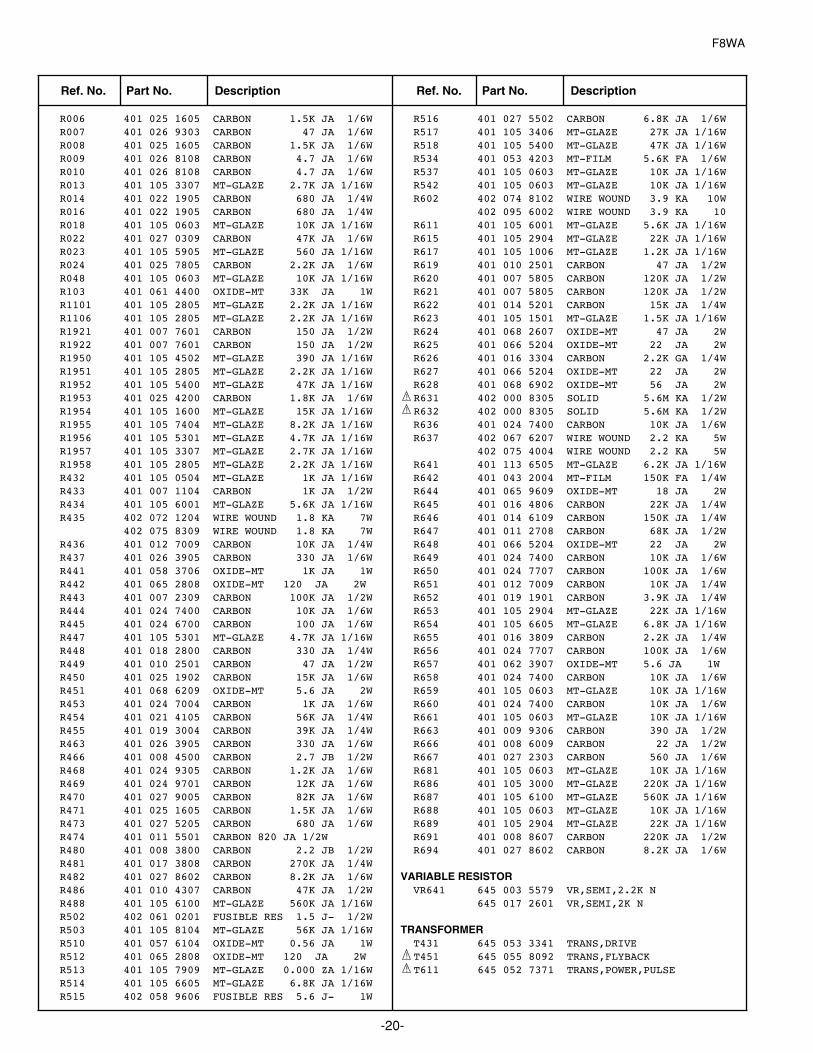
-20-
F8WA
R006 401 025 1605 CARBON 1.5K JA 1/6W R007 401 026 9303 CARBON 47 JA 1/6W R008 401 025 1605 CARBON 1.5K JA 1/6W R009 401 026 8108 CARBON 4.7 JA 1/6W R010 401 026 8108 CARBON 4.7 JA 1/6W R013 401 105 3307 MT-GLAZE 2.7K JA 1/16W R014 401 022 1905 CARBON 680 JA 1/4W R016 401 022 1905 CARBON 680 JA 1/4W R018 401 105 0603 MT-GLAZE 10K JA 1/16W R022 401 027 0309 CARBON 47K JA 1/6W R023 401 105 5905 MT-GLAZE 560 JA 1/16W R024 401 025 7805 CARBON 2.2K JA 1/6W R048 401 105 0603 MT-GLAZE 10K JA 1/16W R103 401 061 4400 OXIDE-MT 33K JA 1W R1101 401 105 2805 MT-GLAZE 2.2K JA 1/16W R1106 401 105 2805 MT-GLAZE 2.2K JA 1/16W R1921 401 007 7601 CARBON 150 JA 1/2W R1922 401 007 7601 CARBON 150 JA 1/2W R1950 401 105 4502 MT-GLAZE 390 JA 1/16W R1951 401 105 2805 MT-GLAZE 2.2K JA 1/16W R1952 401 105 5400 MT-GLAZE 47K JA 1/16W R1953 401 025 4200 CARBON 1.8K JA 1/6W R1954 401 105 1600 MT-GLAZE 15K JA 1/16W R1955 401 105 7404 MT-GLAZE 8.2K JA 1/16W R1956 401 105 5301 MT-GLAZE 4.7K JA 1/16W R1957 401 105 3307 MT-GLAZE 2.7K JA 1/16W R1958 401 105 2805 MT-GLAZE 2.2K JA 1/16W R432 401 105 0504 MT-GLAZE 1K JA 1/16W R433 401 007 1104 CARBON 1K JA 1/2W R434 401 105 6001 MT-GLAZE 5.6K JA 1/16W R435 402 072 1204 WIRE WOUND 1.8 KA 7W
402 075 8309 WIRE WOUND 1.8 KA 7W R436 401 012 7009 CARBON 10K JA 1/4W R437 401 026 3905 CARBON 330 JA 1/6W R441 401 058 3706 OXIDE-MT 1K JA 1W R442 401 065 2808 OXIDE-MT 120 JA 2W R443 401 007 2309 CARBON 100K JA 1/2W R444 401 024 7400 CARBON 10K JA 1/6W R445 401 024 6700 CARBON 100 JA 1/6W R447 401 105 5301 MT-GLAZE 4.7K JA 1/16W R448 401 018 2800 CARBON 330 JA 1/4W R449 401 010 2501 CARBON 47 JA 1/2W R450 401 025 1902 CARBON 15K JA 1/6W R451 401 068 6209 OXIDE-MT 5.6 JA 2W R453 401 024 7004 CARBON 1K JA 1/6W R454 401 021 4105 CARBON 56K JA 1/4W R455 401 019 3004 CARBON 39K JA 1/4W R463 401 026 3905 CARBON 330 JA 1/6W R466 401 008 4500 CARBON 2.7 JB 1/2W R468 401 024 9305 CARBON 1.2K JA 1/6W R469 401 024 9701 CARBON 12K JA 1/6W R470 401 027 9005 CARBON 82K JA 1/6W R471 401 025 1605 CARBON 1.5K JA 1/6W R473 401 027 5205 CARBON 680 JA 1/6W R474 401 011 5501 CARBON 820 JA 1/2W R480 401 008 3800 CARBON 2.2 JB 1/2W R481 401 017 3808 CARBON 270K JA 1/4W R482 401 027 8602 CARBON 8.2K JA 1/6W R486 401 010 4307 CARBON 47K JA 1/2W R488 401 105 6100 MT-GLAZE 560K JA 1/16W R502 402 061 0201 FUSIBLE RES 1.5 J- 1/2W R503 401 105 8104 MT-GLAZE 56K JA 1/16W R510 401 057 6104 OXIDE-MT 0.56 JA 1W R512 401 065 2808 OXIDE-MT 120 JA 2W R513 401 105 7909 MT-GLAZE 0.000 ZA 1/16W R514 401 105 6605 MT-GLAZE 6.8K JA 1/16W R515 402 058 9606 FUSIBLE RES 5.6 J- 1W
R516 401 027 5502 CARBON 6.8K JA 1/6W R517 401 105 3406 MT-GLAZE 27K JA 1/16W R518 401 105 5400 MT-GLAZE 47K JA 1/16W R534 401 053 4203 MT-FILM 5.6K FA 1/6W R537 401 105 0603 MT-GLAZE 10K JA 1/16W R542 401 105 0603 MT-GLAZE 10K JA 1/16W R602 402 074 8102 WIRE WOUND 3.9 KA 10W
402 095 6002 WIRE WOUND 3.9 KA 10 R611 401 105 6001 MT-GLAZE 5.6K JA 1/16W R615 401 105 2904 MT-GLAZE 22K JA 1/16W R617 401 105 1006 MT-GLAZE 1.2K JA 1/16W R619 401 010 2501 CARBON 47 JA 1/2W R620 401 007 5805 CARBON 120K JA 1/2W R621 401 007 5805 CARBON 120K JA 1/2W R622 401 014 5201 CARBON 15K JA 1/4W R623 401 105 1501 MT-GLAZE 1.5K JA 1/16W R624 401 068 2607 OXIDE-MT 47 JA 2W R625 401 066 5204 OXIDE-MT 22 JA 2W R626 401 016 3304 CARBON 2.2K GA 1/4W R627 401 066 5204 OXIDE-MT 22 JA 2W R628 401 068 6902 OXIDE-MT 56 JA 2W R631 402 000 8305 SOLID 5.6M KA 1/2W R632 402 000 8305 SOLID 5.6M KA 1/2W R636 401 024 7400 CARBON 10K JA 1/6W R637 402 067 6207 WIRE WOUND 2.2 KA 5W
402 075 4004 WIRE WOUND 2.2 KA 5W R641 401 113 6505 MT-GLAZE 6.2K JA 1/16W R642 401 043 2004 MT-FILM 150K FA 1/4W R644 401 065 9609 OXIDE-MT 18 JA 2W R645 401 016 4806 CARBON 22K JA 1/4W R646 401 014 6109 CARBON 150K JA 1/4W R647 401 011 2708 CARBON 68K JA 1/2W R648 401 066 5204 OXIDE-MT 22 JA 2W R649 401 024 7400 CARBON 10K JA 1/6W R650 401 024 7707 CARBON 100K JA 1/6W R651 401 012 7009 CARBON 10K JA 1/4W R652 401 019 1901 CARBON 3.9K JA 1/4W R653 401 105 2904 MT-GLAZE 22K JA 1/16W R654 401 105 6605 MT-GLAZE 6.8K JA 1/16W R655 401 016 3809 CARBON 2.2K JA 1/4W R656 401 024 7707 CARBON 100K JA 1/6W R657 401 062 3907 OXIDE-MT 5.6 JA 1W R658 401 024 7400 CARBON 10K JA 1/6W R659 401 105 0603 MT-GLAZE 10K JA 1/16W R660 401 024 7400 CARBON 10K JA 1/6W R661 401 105 0603 MT-GLAZE 10K JA 1/16W R663 401 009 9306 CARBON 390 JA 1/2W R666 401 008 6009 CARBON 22 JA 1/2W R667 401 027 2303 CARBON 560 JA 1/6W R681 401 105 0603 MT-GLAZE 10K JA 1/16W R686 401 105 3000 MT-GLAZE 220K JA 1/16W R687 401 105 6100 MT-GLAZE 560K JA 1/16W R688 401 105 0603 MT-GLAZE 10K JA 1/16W R689 401 105 2904 MT-GLAZE 22K JA 1/16W R691 401 008 8607 CARBON 220K JA 1/2W R694 401 027 8602 CARBON 8.2K JA 1/6W
VARIABLE RESISTORVR641 645 003 5579 VR,SEMI,2.2K N
645 017 2601 VR,SEMI,2K N
TRANSFORMERT431 645 053 3341 TRANS,DRIVE T451 645 055 8092 TRANS,FLYBACK T611 645 052 7371 TRANS,POWER,PULSE !
!
!
!
Ref. No. Part No. Description Ref. No. Part No. Description

COILL1101 645 001 4567 INDUCTOR,10U K L1106 645 001 4567 INDUCTOR,10U K L1921 645 002 1787 CORE,PIPE
645 033 2722 CORE,PIPE L1922 645 007 9559 INDUCTOR,12U J L1923 645 007 9559 INDUCTOR,12U J L431 645 008 5628 INDUCTOR,1U M
645 026 1084 INDUCTOR,1U K 645 036 4198 INDUCTOR,1.0U,FILTER 645 052 5919 INDUCTOR,1.0U,FILTER
L441 645 064 2654 COIL,LINEARITY L443 610 211 3471 INDUCTOR
645 005 5652 INDUCTOR,6800U K L461 610 031 1367 INDUCTOR 202J
610 211 3488 INDUCTOR 645 005 5645 INDUCTOR,2200U K 645 007 8361 INDUCTOR,2000U
L462 610 000 0186 COIL 645 016 9144 INDUCTOR,650UH
L611 645 007 8248 INDUCTOR,22U K 610 031 1572 INDUCTOR,22U K 645 005 5515 INDUCTOR,22U K
L612 610 031 9998 PIPE CORE 645 018 7025 CORE,PIPE 652 001 0475 PIPE CORE
L691C 645 067 2668 LINE FILTER L692 652 000 1817 CORE,PIPE
652 000 1749 CORE,PIPE 610 237 1000 PIPE CORE
L693 652 000 1817 CORE,PIPE 652 000 1749 CORE,PIPE 610 237 1000 PIPE CORE
DIODED041 407 012 4406 DIODE 1SS133 D1102 407 012 4406 DIODE 1SS133 D1103 407 012 4406 DIODE 1SS133 D1951 407 116 6504 LED SLP-181B-51 D1951A 610 273 7929 HOLDER LED-S4KF
610 303 9954 HOLDER LED-C4LA D431 407 099 6003 ZENER DIODE MTZJ9.1B
408 048 0103 ZENER DIODE MTZJ9.1B D438 407 095 8001 DIODE ERD07-15L D439 407 006 4108 DIODE ERB44-04V1 D441 407 104 2402 PHOTO COUPLE PC817C
407 106 6101 PHOTO COUPLE PC817D 407 002 6809 PHOTO COUPLE TLP521-1-BL
D442 407 149 0807 DIODE 1SS355-TE-17 D445 407 149 0807 DIODE 1SS355-TE-17 D446 407 063 9504 ZENER DIODE MTZJ8.2B D449 407 005 7308 DIODE EM01Z
407 005 8602 DIODE ERA15-02-V1 D461 407 012 4406 DIODE 1SS133 D463 407 012 4406 DIODE 1SS133 D465 407 012 4406 DIODE 1SS133 D466 407 099 7901 ZENER DIODE MTZJ20B
408 047 5901 ZENER DIODE MTZJ20B-52 D469 407 005 9609 DIODE ERA22-04-V1
407 007 7405 DIODE EU1 D481 407 005 9609 DIODE ERA22-04-V1
407 007 7405 DIODE EU1 D482 407 012 4406 DIODE 1SS133 D501 407 005 7308 DIODE EM01Z
407 005 8602 DIODE ERA15-02-V1 D502 407 149 0807 DIODE 1SS355-TE-17 D503 407 063 9108 ZENER DIODE MTZJ6.8B
D504 407 149 0807 DIODE 1SS355-TE-17 D603 407 006 6300 DIODE ERC05-10BV1
407 009 6901 DIODE RM11C D604 407 006 6300 DIODE ERC05-10BV1
407 009 6901 DIODE RM11C D605 407 006 6300 DIODE ERC05-10BV1
407 009 6901 DIODE RM11C D606 407 006 6300 DIODE ERC05-10BV1
407 009 6901 DIODE RM11C D614 407 012 4406 DIODE 1SS133 D615 407 234 8701 PHOTO COUPLE PC123X5YFZ
407 230 3908 PHOTO COUPLE PC123Y52 407 231 7707 PC TLP421F(D4-BL)
D616 407 012 4406 DIODE 1SS133 D617 407 124 6404 DIODE ERA18-04-V1
407 007 6606 DIODE ES1 407 007 6903 DIODE ES1Z
D618 407 012 4406 DIODE 1SS133 D619 407 099 6409 ZENER DIODE MTZJ11B D630 407 006 4009 DIODE ERB44-02V1
407 007 7603 DIODE EU2 407 007 7801 DIODE EU2Z
D633 407 166 2303 DIODE ERC91-02 D635 407 129 6706 DIODE RU4YX LF-L1 D637 407 012 4406 DIODE 1SS133 D641 407 149 0807 DIODE 1SS355-TE-17 D642 407 129 7000 DIODE RU4AM LF-L1 D643 407 149 0807 DIODE 1SS355-TE-17 D644 407 149 0807 DIODE 1SS355-TE-17 D645 407 099 5402 ZENER DIODE MTZJ6.2B D646 407 149 0807 DIODE 1SS355-TE-17 D647 407 149 0807 DIODE 1SS355-TE-17 D648 407 106 2806 DIODE RU3YX D666 407 099 5303 ZENER DIODE MTZJ5.6B
408 047 7400 ZENER DIODE MTZJ5.6B D683 407 149 0807 DIODE 1SS355-TE-17 D685 407 099 5402 ZENER DIODE MTZJ6.2B D691 407 012 4406 DIODE 1SS133
MISCELLANEOUSF691 423 028 8603 FUSE 250V 4A
423 024 8409 FUSE 250V 4A 423 007 2103 FUSE 250V 4A
F691-1 645 000 5077 HOLDER,FUSE 645 040 3576 HOLDER,FUSE
F691-2 645 000 5077 HOLDER,FUSE 645 040 3576 HOLDER,FUSE
A1901 645 047 6228 UNIT,REMOCON RECEIVER K1101 645 016 6426 JACK,RCA-3 K1921 645 027 8761 JACK,PHONE D3.6
645 006 4708 JACK,PHONE D3.6 PS691 408 046 4301 THERMISTOR PTDAA1BF4R5Q20RL691 645 028 2713 RELAY
645 030 5597 RELAY SW1951 645 003 4701 SWITCH,PUSH 1P-1TX1
645 019 4887 SWITCH,PUSH 1P-1TX1 645 027 7382 SWITCH,PUSH 1P-1TX1
SW1952 645 003 4701 SWITCH,PUSH 1P-1TX1 645 019 4887 SWITCH,PUSH 1P-1TX1 645 027 7382 SWITCH,PUSH 1P-1TX1
SW1953 645 003 4701 SWITCH,PUSH 1P-1TX1 645 019 4887 SWITCH,PUSH 1P-1TX1 645 027 7382 SWITCH,PUSH 1P-1TX1
SW1954 645 003 4701 SWITCH,PUSH 1P-1TX1 645 019 4887 SWITCH,PUSH 1P-1TX1 645 027 7382 SWITCH,PUSH 1P-1TX1
SW1955 645 003 4701 SWITCH,PUSH 1P-1TX1
!
!
!
!
!
-21-
F8WA
Ref. No. Part No. Description Ref. No. Part No. Description

-22-
F8WA
645 019 4887 SWITCH,PUSH 1P-1TX1 645 027 7382 SWITCH,PUSH 1P-1TX1
SW1956 645 003 4701 SWITCH,PUSH 1P-1TX1 645 019 4887 SWITCH,PUSH 1P-1TX1 645 027 7382 SWITCH,PUSH 1P-1TX1
SW691 645 059 0061 SWITCH, POWER 1P-1TX1VA691 407 171 2008 VARISTOR ERZV14D471
610 311 6341 ASSY,PWB,SUB F8WA1AA0B10E6870A
TRANSISTORQ1202 405 014 4509 TR 2SC2412K T146 R
405 014 4608 TR 2SC2412K T146 S 405 015 8704 TR 2SC2812-L6-TB 405 015 8902 TR 2SC2812-L7-TB 405 163 1602 TR 2SC2812N-L6-TB0 405 163 1701 TR 2SC2812N-L7-TB0 405 173 9803 TR 2SC3928A1R 405 173 9902 TR 2SC3928A1S
Q1206 405 014 4509 TR 2SC2412K T146 R 405 014 4608 TR 2SC2412K T146 S 405 015 8704 TR 2SC2812-L6-TB 405 015 8902 TR 2SC2812-L7-TB 405 163 1602 TR 2SC2812N-L6-TB0 405 163 1701 TR 2SC2812N-L7-TB0 405 173 9803 TR 2SC3928A1R 405 173 9902 TR 2SC3928A1S
Q121 405 014 4509 TR 2SC2412K T146 R 405 014 4608 TR 2SC2412K T146 S 405 015 8704 TR 2SC2812-L6-TB 405 015 8902 TR 2SC2812-L7-TB 405 163 1602 TR 2SC2812N-L6-TB0 405 163 1701 TR 2SC2812N-L7-TB0 405 173 9803 TR 2SC3928A1R 405 173 9902 TR 2SC3928A1S
Q133 405 014 4509 TR 2SC2412K T146 R 405 014 4608 TR 2SC2412K T146 S 405 015 8704 TR 2SC2812-L6-TB 405 015 8902 TR 2SC2812-L7-TB 405 163 1602 TR 2SC2812N-L6-TB0 405 163 1701 TR 2SC2812N-L7-TB0 405 173 9803 TR 2SC3928A1R 405 173 9902 TR 2SC3928A1S
Q153 405 134 5905 TR 2SA1037AK-T146-R 405 147 2205 TR 2SA1037AK-S-T146 405 002 0308 TR 2SA1037K T146 R 405 002 0407 TR 2SA1037K T146 S 405 002 6706 TR 2SA1179-M6-TB 405 002 6904 TR 2SA1179-M7-TB 405 163 1503 TR 2SA1179N-M6-TB 405 163 2708 TR 2SA1179N-M7-TB 405 173 9605 TR 2SA1235A1E 405 173 9704 TR 2SA1235A1F
Q162 405 014 4509 TR 2SC2412K T146 R 405 014 4608 TR 2SC2412K T146 S 405 015 8704 TR 2SC2812-L6-TB 405 015 8902 TR 2SC2812-L7-TB 405 163 1602 TR 2SC2812N-L6-TB0 405 163 1701 TR 2SC2812N-L7-TB0 405 173 9803 TR 2SC3928A1R 405 173 9902 TR 2SC3928A1S
Q211 405 134 5905 TR 2SA1037AK-T146-R 405 147 2205 TR 2SA1037AK-S-T146 405 002 0308 TR 2SA1037K T146 R 405 002 0407 TR 2SA1037K T146 S
405 002 6706 TR 2SA1179-M6-TB 405 002 6904 TR 2SA1179-M7-TB 405 163 1503 TR 2SA1179N-M6-TB 405 163 2708 TR 2SA1179N-M7-TB 405 173 9605 TR 2SA1235A1E 405 173 9704 TR 2SA1235A1F
Q242 405 134 5905 TR 2SA1037AK-T146-R 405 147 2205 TR 2SA1037AK-S-T146 405 002 0308 TR 2SA1037K T146 R 405 002 0407 TR 2SA1037K T146 S 405 002 6706 TR 2SA1179-M6-TB 405 002 6904 TR 2SA1179-M7-TB 405 163 1503 TR 2SA1179N-M6-TB 405 163 2708 TR 2SA1179N-M7-TB 405 173 9605 TR 2SA1235A1E 405 173 9704 TR 2SA1235A1F
Q243 405 134 5905 TR 2SA1037AK-T146-R 405 147 2205 TR 2SA1037AK-S-T146 405 002 0308 TR 2SA1037K T146 R 405 002 0407 TR 2SA1037K T146 S 405 002 6706 TR 2SA1179-M6-TB 405 002 6904 TR 2SA1179-M7-TB 405 163 1503 TR 2SA1179N-M6-TB 405 163 2708 TR 2SA1179N-M7-TB 405 173 9605 TR 2SA1235A1E 405 173 9704 TR 2SA1235A1F
Q244 405 134 5905 TR 2SA1037AK-T146-R 405 147 2205 TR 2SA1037AK-S-T146 405 002 0308 TR 2SA1037K T146 R 405 002 0407 TR 2SA1037K T146 S 405 002 6706 TR 2SA1179-M6-TB 405 002 6904 TR 2SA1179-M7-TB 405 163 1503 TR 2SA1179N-M6-TB 405 163 2708 TR 2SA1179N-M7-TB 405 173 9605 TR 2SA1235A1E 405 173 9704 TR 2SA1235A1F
Q3452 405 014 4509 TR 2SC2412K T146 R 405 014 4608 TR 2SC2412K T146 S 405 015 8704 TR 2SC2812-L6-TB 405 015 8902 TR 2SC2812-L7-TB 405 163 1602 TR 2SC2812N-L6-TB0 405 163 1701 TR 2SC2812N-L7-TB0 405 173 9803 TR 2SC3928A1R 405 173 9902 TR 2SC3928A1S
Q3453 405 014 4509 TR 2SC2412K T146 R 405 014 4608 TR 2SC2412K T146 S 405 015 8704 TR 2SC2812-L6-TB 405 015 8902 TR 2SC2812-L7-TB 405 163 1602 TR 2SC2812N-L6-TB0 405 163 1701 TR 2SC2812N-L7-TB0 405 173 9803 TR 2SC3928A1R 405 173 9902 TR 2SC3928A1S
Q3454 405 014 4509 TR 2SC2412K T146 R 405 014 4608 TR 2SC2412K T146 S 405 015 8704 TR 2SC2812-L6-TB 405 015 8902 TR 2SC2812-L7-TB 405 163 1602 TR 2SC2812N-L6-TB0 405 163 1701 TR 2SC2812N-L7-TB0 405 173 9803 TR 2SC3928A1R 405 173 9902 TR 2SC3928A1S
Q3455 405 014 4509 TR 2SC2412K T146 R 405 014 4608 TR 2SC2412K T146 S 405 015 8704 TR 2SC2812-L6-TB 405 015 8902 TR 2SC2812-L7-TB 405 163 1602 TR 2SC2812N-L6-TB0 405 163 1701 TR 2SC2812N-L7-TB0 405 173 9803 TR 2SC3928A1R
!
!
Ref. No. Part No. Description Ref. No. Part No. Description

405 173 9902 TR 2SC3928A1S Q491 405 014 4509 TR 2SC2412K T146 R
405 014 4608 TR 2SC2412K T146 S 405 015 8704 TR 2SC2812-L6-TB 405 015 8902 TR 2SC2812-L7-TB 405 163 1602 TR 2SC2812N-L6-TB0 405 163 1701 TR 2SC2812N-L7-TB0 405 173 9803 TR 2SC3928A1R 405 173 9902 TR 2SC3928A1S
Q804 405 014 4509 TR 2SC2412K T146 R 405 014 4608 TR 2SC2412K T146 S 405 015 8704 TR 2SC2812-L6-TB 405 015 8902 TR 2SC2812-L7-TB 405 163 1602 TR 2SC2812N-L6-TB0 405 163 1701 TR 2SC2812N-L7-TB0 405 173 9803 TR 2SC3928A1R 405 173 9902 TR 2SC3928A1S
Q805 405 014 4509 TR 2SC2412K T146 R 405 014 4608 TR 2SC2412K T146 S 405 015 8704 TR 2SC2812-L6-TB 405 015 8902 TR 2SC2812-L7-TB 405 163 1602 TR 2SC2812N-L6-TB0 405 163 1701 TR 2SC2812N-L7-TB0 405 173 9803 TR 2SC3928A1R 405 173 9902 TR 2SC3928A1S
Q807 405 134 5905 TR 2SA1037AK-T146-R 405 147 2205 TR 2SA1037AK-S-T146 405 002 0308 TR 2SA1037K T146 R 405 002 0407 TR 2SA1037K T146 S 405 002 6706 TR 2SA1179-M6-TB 405 002 6904 TR 2SA1179-M7-TB 405 163 1503 TR 2SA1179N-M6-TB 405 163 2708 TR 2SA1179N-M7-TB 405 173 9605 TR 2SA1235A1E 405 173 9704 TR 2SA1235A1F
Q808 405 014 4509 TR 2SC2412K T146 R 405 014 4608 TR 2SC2412K T146 S 405 015 8704 TR 2SC2812-L6-TB 405 015 8902 TR 2SC2812-L7-TB 405 163 1602 TR 2SC2812N-L6-TB0 405 163 1701 TR 2SC2812N-L7-TB0 405 173 9803 TR 2SC3928A1R 405 173 9902 TR 2SC3928A1S
INTEGRATED CIRCUITIC1201 409 161 3408 IC LA7954 IC201 409 559 3201 IC TB1262AF IC3451 409 445 1403 IC TDA9875A/V2 IC801 410 508 8208 IC ST92195C8B1/MCY IC803 409 495 7103 IC CAT24WC08P
QM24C08-BN6- IC M24C08-BN6 410 495 7901 IC AT24C08A-10PI-2.7 409 383 6805 IC 24LC08B/P
CAPACITOR C056 403 157 6800 CERAMIC 680P K 50V C101 404 087 4904 ELECT 47U M 25V
403 047 3100 ELECT 47U M 25V C102 403 039 3507 ELECT 470U M 6.3V C103 403 039 3507 ELECT 470U M 6.3V C104 404 084 8905 ELECT 10U M 50V
403 049 4204 ELECT 10U M 50V C109 403 215 2201 CERAMIC 0.01U K 50V C110 403 215 2201 CERAMIC 0.01U K 50V C113 403 069 8305 CERAMIC 0.01U Z 50V C120 404 087 4904 ELECT 47U M 25V
403 047 3100 ELECT 47U M 25V
C1200 404 084 8905 ELECT 10U M 50V 403 049 4204 ELECT 10U M 50V
C1202 404 087 4904 ELECT 47U M 25V 403 047 3100 ELECT 47U M 25V
C1203 403 215 2201 CERAMIC 0.01U K 50V C1204 404 084 8905 ELECT 10U M 50V
403 049 4204 ELECT 10U M 50V C1205 404 084 8905 ELECT 10U M 50V
403 049 4204 ELECT 10U M 50V C1206 403 145 9905 CERAMIC 22P J 50V C121 403 215 2201 CERAMIC 0.01U K 50V C1213 404 084 8905 ELECT 10U M 50V
403 049 4204 ELECT 10U M 50V C123 403 215 2201 CERAMIC 0.01U K 50V C124 404 084 8905 ELECT 10U M 50V
403 049 4204 ELECT 10U M 50V C125 404 084 9001 ELECT 2.2U M 50V
403 049 9803 ELECT 2.2U M 50V C126 403 314 5905 CERAMIC 0.47U K 16V
403 307 8807 CERAMIC 0.47U K 16V C127 403 215 2201 CERAMIC 0.01U K 50V C128 403 040 3701 ELECT 220U M 10V C135 403 215 2201 CERAMIC 0.01U K 50V C137 403 215 2201 CERAMIC 0.01U K 50V C138 401 105 7909 MT-GLAZE 0.000 ZA 1/16W C139 404 087 4904 ELECT 47U M 25V
403 047 3100 ELECT 47U M 25V C140 403 179 3801 POLYESTER 0.01U K 50V C143 401 105 7909 MT-GLAZE 0.000 ZA 1/16W C144 403 323 8805 CERAMIC 2.2U Z 16V
403 322 6109 CERAMIC 2.2U Z 16V C145 401 105 7909 MT-GLAZE 0.000 ZA 1/16W C146 404 087 4904 ELECT 47U M 25V
403 047 3100 ELECT 47U M 25V C202 403 113 4109 CERAMIC 2200P K 50V C203 403 314 5905 CERAMIC 0.47U K 16V
403 307 8807 CERAMIC 0.47U K 16V C206 403 215 2201 CERAMIC 0.01U K 50V C207 403 215 2201 CERAMIC 0.01U K 50V C208 404 087 4904 ELECT 47U M 25V
403 047 3100 ELECT 47U M 25V C209 403 207 0307 CERAMIC 1U Z 16 C210 403 207 0307 CERAMIC 1U Z 16 C212 403 157 7104 CERAMIC 2700P K 50V C213 404 087 4904 ELECT 47U M 25V
403 047 3100 ELECT 47U M 25V C216 404 084 8905 ELECT 10U M 50V
403 049 4204 ELECT 10U M 50V C218 403 215 2201 CERAMIC 0.01U K 50V C219 403 155 2408 CERAMIC 5600P K 50V C220 404 084 8806 ELECT 1U M 50V
403 049 0008 ELECT 1U M 50V C221 403 215 2201 CERAMIC 0.01U K 50V C222 403 215 2201 CERAMIC 0.01U K 50V C223 403 215 2201 CERAMIC 0.01U K 50V C230 403 269 5906 CERAMIC 0.22U K 16V C231 403 113 4109 CERAMIC 2200P K 50V C232 403 233 3808 CERAMIC 10P C 50V C233 404 087 4904 ELECT 47U M 25V
403 047 3100 ELECT 47U M 25V C234 403 164 0204 CERAMIC 0.1U Z 25V C235 403 164 0204 CERAMIC 0.1U Z 25V C236 403 164 0204 CERAMIC 0.1U Z 25V C237 403 164 0204 CERAMIC 0.1U Z 25V C238 403 139 6903 CERAMIC 1P C 50V C241 403 067 7805 MT-COMPO 0.47U J 50V
403 256 0808 MT-COMPO 0.47U J 50V
-23-
F8WA
Ref. No. Part No. Description Ref. No. Part No. Description
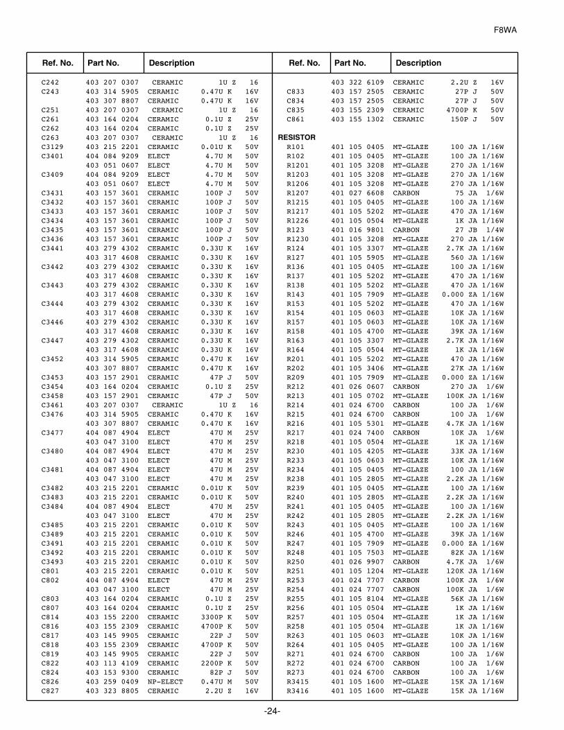
-24-
F8WA
C242 403 207 0307 CERAMIC 1U Z 16 C243 403 314 5905 CERAMIC 0.47U K 16V
403 307 8807 CERAMIC 0.47U K 16V C251 403 207 0307 CERAMIC 1U Z 16 C261 403 164 0204 CERAMIC 0.1U Z 25V C262 403 164 0204 CERAMIC 0.1U Z 25V C263 403 207 0307 CERAMIC 1U Z 16 C3129 403 215 2201 CERAMIC 0.01U K 50V C3401 404 084 9209 ELECT 4.7U M 50V
403 051 0607 ELECT 4.7U M 50V C3409 404 084 9209 ELECT 4.7U M 50V
403 051 0607 ELECT 4.7U M 50V C3431 403 157 3601 CERAMIC 100P J 50V C3432 403 157 3601 CERAMIC 100P J 50V C3433 403 157 3601 CERAMIC 100P J 50V C3434 403 157 3601 CERAMIC 100P J 50V C3435 403 157 3601 CERAMIC 100P J 50V C3436 403 157 3601 CERAMIC 100P J 50V C3441 403 279 4302 CERAMIC 0.33U K 16V
403 317 4608 CERAMIC 0.33U K 16V C3442 403 279 4302 CERAMIC 0.33U K 16V
403 317 4608 CERAMIC 0.33U K 16V C3443 403 279 4302 CERAMIC 0.33U K 16V
403 317 4608 CERAMIC 0.33U K 16V C3444 403 279 4302 CERAMIC 0.33U K 16V
403 317 4608 CERAMIC 0.33U K 16V C3446 403 279 4302 CERAMIC 0.33U K 16V
403 317 4608 CERAMIC 0.33U K 16V C3447 403 279 4302 CERAMIC 0.33U K 16V
403 317 4608 CERAMIC 0.33U K 16V C3452 403 314 5905 CERAMIC 0.47U K 16V
403 307 8807 CERAMIC 0.47U K 16V C3453 403 157 2901 CERAMIC 47P J 50V C3454 403 164 0204 CERAMIC 0.1U Z 25V C3458 403 157 2901 CERAMIC 47P J 50V C3461 403 207 0307 CERAMIC 1U Z 16 C3476 403 314 5905 CERAMIC 0.47U K 16V
403 307 8807 CERAMIC 0.47U K 16V C3477 404 087 4904 ELECT 47U M 25V
403 047 3100 ELECT 47U M 25V C3480 404 087 4904 ELECT 47U M 25V
403 047 3100 ELECT 47U M 25V C3481 404 087 4904 ELECT 47U M 25V
403 047 3100 ELECT 47U M 25V C3482 403 215 2201 CERAMIC 0.01U K 50V C3483 403 215 2201 CERAMIC 0.01U K 50V C3484 404 087 4904 ELECT 47U M 25V
403 047 3100 ELECT 47U M 25V C3485 403 215 2201 CERAMIC 0.01U K 50V C3489 403 215 2201 CERAMIC 0.01U K 50V C3491 403 215 2201 CERAMIC 0.01U K 50V C3492 403 215 2201 CERAMIC 0.01U K 50V C3493 403 215 2201 CERAMIC 0.01U K 50V C801 403 215 2201 CERAMIC 0.01U K 50V C802 404 087 4904 ELECT 47U M 25V
403 047 3100 ELECT 47U M 25V C803 403 164 0204 CERAMIC 0.1U Z 25V C807 403 164 0204 CERAMIC 0.1U Z 25V C814 403 155 2200 CERAMIC 3300P K 50V C816 403 155 2309 CERAMIC 4700P K 50V C817 403 145 9905 CERAMIC 22P J 50V C818 403 155 2309 CERAMIC 4700P K 50V C819 403 145 9905 CERAMIC 22P J 50V C822 403 113 4109 CERAMIC 2200P K 50V C824 403 153 9300 CERAMIC 82P J 50V C826 403 259 0409 NP-ELECT 0.47U M 50V C827 403 323 8805 CERAMIC 2.2U Z 16V
403 322 6109 CERAMIC 2.2U Z 16V C833 403 157 2505 CERAMIC 27P J 50V C834 403 157 2505 CERAMIC 27P J 50V C835 403 155 2309 CERAMIC 4700P K 50V C861 403 155 1302 CERAMIC 150P J 50V
RESISTORR101 401 105 0405 MT-GLAZE 100 JA 1/16W R102 401 105 0405 MT-GLAZE 100 JA 1/16W R1201 401 105 3208 MT-GLAZE 270 JA 1/16W R1203 401 105 3208 MT-GLAZE 270 JA 1/16W R1206 401 105 3208 MT-GLAZE 270 JA 1/16W R1207 401 027 6608 CARBON 75 JA 1/6W R1215 401 105 0405 MT-GLAZE 100 JA 1/16W R1217 401 105 5202 MT-GLAZE 470 JA 1/16W R1226 401 105 0504 MT-GLAZE 1K JA 1/16W R123 401 016 9801 CARBON 27 JB 1/4W R1230 401 105 3208 MT-GLAZE 270 JA 1/16W R124 401 105 3307 MT-GLAZE 2.7K JA 1/16W R127 401 105 5905 MT-GLAZE 560 JA 1/16W R136 401 105 0405 MT-GLAZE 100 JA 1/16W R137 401 105 5202 MT-GLAZE 470 JA 1/16W R138 401 105 5202 MT-GLAZE 470 JA 1/16W R143 401 105 7909 MT-GLAZE 0.000 ZA 1/16W R153 401 105 5202 MT-GLAZE 470 JA 1/16W R154 401 105 0603 MT-GLAZE 10K JA 1/16W R157 401 105 0603 MT-GLAZE 10K JA 1/16W R158 401 105 4700 MT-GLAZE 39K JA 1/16W R163 401 105 3307 MT-GLAZE 2.7K JA 1/16W R164 401 105 0504 MT-GLAZE 1K JA 1/16W R201 401 105 5202 MT-GLAZE 470 JA 1/16W R202 401 105 3406 MT-GLAZE 27K JA 1/16W R209 401 105 7909 MT-GLAZE 0.000 ZA 1/16W R212 401 026 0607 CARBON 270 JA 1/6W R213 401 105 0702 MT-GLAZE 100K JA 1/16W R214 401 024 6700 CARBON 100 JA 1/6W R215 401 024 6700 CARBON 100 JA 1/6W R216 401 105 5301 MT-GLAZE 4.7K JA 1/16W R217 401 024 7400 CARBON 10K JA 1/6W R218 401 105 0504 MT-GLAZE 1K JA 1/16W R230 401 105 4205 MT-GLAZE 33K JA 1/16W R233 401 105 0603 MT-GLAZE 10K JA 1/16W R234 401 105 0405 MT-GLAZE 100 JA 1/16W R238 401 105 2805 MT-GLAZE 2.2K JA 1/16W R239 401 105 0405 MT-GLAZE 100 JA 1/16W R240 401 105 2805 MT-GLAZE 2.2K JA 1/16W R241 401 105 0405 MT-GLAZE 100 JA 1/16W R242 401 105 2805 MT-GLAZE 2.2K JA 1/16W R243 401 105 0405 MT-GLAZE 100 JA 1/16W R246 401 105 4700 MT-GLAZE 39K JA 1/16W R247 401 105 7909 MT-GLAZE 0.000 ZA 1/16W R248 401 105 7503 MT-GLAZE 82K JA 1/16W R250 401 026 9907 CARBON 4.7K JA 1/6W R251 401 105 1204 MT-GLAZE 120K JA 1/16W R253 401 024 7707 CARBON 100K JA 1/6W R254 401 024 7707 CARBON 100K JA 1/6W R255 401 105 8104 MT-GLAZE 56K JA 1/16W R256 401 105 0504 MT-GLAZE 1K JA 1/16W R257 401 105 0504 MT-GLAZE 1K JA 1/16W R258 401 105 0504 MT-GLAZE 1K JA 1/16W R263 401 105 0603 MT-GLAZE 10K JA 1/16W R264 401 105 0405 MT-GLAZE 100 JA 1/16W R271 401 024 6700 CARBON 100 JA 1/6W R272 401 024 6700 CARBON 100 JA 1/6W R273 401 024 6700 CARBON 100 JA 1/6W R3415 401 105 1600 MT-GLAZE 15K JA 1/16W R3416 401 105 1600 MT-GLAZE 15K JA 1/16W
Ref. No. Part No. Description Ref. No. Part No. Description

R3441 401 105 1600 MT-GLAZE 15K JA 1/16W R3442 401 105 1600 MT-GLAZE 15K JA 1/16W R3443 401 105 1600 MT-GLAZE 15K JA 1/16W R3444 401 105 1600 MT-GLAZE 15K JA 1/16W R3451 401 024 6700 CARBON 100 JA 1/6W R3452 401 024 6700 CARBON 100 JA 1/6W R3453 401 105 0603 MT-GLAZE 10K JA 1/16W R3471 401 105 3208 MT-GLAZE 270 JA 1/16W R3473 401 105 5202 MT-GLAZE 470 JA 1/16W R3474 401 105 2805 MT-GLAZE 2.2K JA 1/16W R3475 401 105 5202 MT-GLAZE 470 JA 1/16W R3476 401 105 2805 MT-GLAZE 2.2K JA 1/16W R3485 401 105 5202 MT-GLAZE 470 JA 1/16W R3486 401 105 2805 MT-GLAZE 2.2K JA 1/16W R3487 401 105 5202 MT-GLAZE 470 JA 1/16W R3488 401 105 2805 MT-GLAZE 2.2K JA 1/16W R464 401 024 6700 CARBON 100 JA 1/6W R491 401 105 3307 MT-GLAZE 2.7K JA 1/16W R492 401 105 0603 MT-GLAZE 10K JA 1/16W R808 401 024 6700 CARBON 100 JA 1/6W R809 401 105 0603 MT-GLAZE 10K JA 1/16W R815 401 024 6700 CARBON 100 JA 1/6W R817 401 024 6700 CARBON 100 JA 1/6W R823 401 024 6700 CARBON 100 JA 1/6W R824 401 024 6700 CARBON 100 JA 1/6W R826 401 025 7409 CARBON 220 JA 1/6W R829 401 105 4205 MT-GLAZE 33K JA 1/16W R830 401 105 4205 MT-GLAZE 33K JA 1/16W R831 401 105 0603 MT-GLAZE 10K JA 1/16W R832 401 105 0603 MT-GLAZE 10K JA 1/16W R838 401 105 6001 MT-GLAZE 5.6K JA 1/16W R839 401 105 6001 MT-GLAZE 5.6K JA 1/16W R840 401 105 0504 MT-GLAZE 1K JA 1/16W R842 401 105 1600 MT-GLAZE 15K JA 1/16W R843 401 026 1000 CARBON 2.7K JA 1/6W R844 401 026 1000 CARBON 2.7K JA 1/6W R845 401 105 3307 MT-GLAZE 2.7K JA 1/16W R847 401 105 4601 MT-GLAZE 3.9K JA 1/16W R848 401 105 4601 MT-GLAZE 3.9K JA 1/16W R849 401 105 4601 MT-GLAZE 3.9K JA 1/16W R852 401 105 3406 MT-GLAZE 27K JA 1/16W R853 401 105 2904 MT-GLAZE 22K JA 1/16W R854 401 105 5301 MT-GLAZE 4.7K JA 1/16W R855 401 105 0603 MT-GLAZE 10K JA 1/16W R856 401 105 5301 MT-GLAZE 4.7K JA 1/16W R857 401 105 4205 MT-GLAZE 33K JA 1/16W R860 401 105 3208 MT-GLAZE 270 JA 1/16W R861 401 105 6506 MT-GLAZE 680 JA 1/16W R862 401 105 7404 MT-GLAZE 8.2K JA 1/16W R863 401 105 1600 MT-GLAZE 15K JA 1/16W R870 401 105 0405 MT-GLAZE 100 JA 1/16W R871 401 105 0603 MT-GLAZE 10K JA 1/16W R872 401 105 4601 MT-GLAZE 3.9K JA 1/16W R873 401 105 4601 MT-GLAZE 3.9K JA 1/16W R874 401 026 9600 CARBON 470 JA 1/6W R875 401 026 9600 CARBON 470 JA 1/6W R880 401 105 4700 MT-GLAZE 39K JA 1/16W R881 401 024 7004 CARBON 1K JA 1/6W R884 401 027 0309 CARBON 47K JA 1/6W R885 401 024 7004 CARBON 1K JA 1/6W
COILL242 645 011 0252 INDUCTOR,2.2U K L243 645 011 0252 INDUCTOR,2.2U K L244 645 011 0252 INDUCTOR,2.2U K L3452 645 011 0252 INDUCTOR,2.2U K L3456 645 011 0252 INDUCTOR,2.2U K
L3457 645 011 0252 INDUCTOR,2.2U K L3459 401 105 7909 MT-GLAZE 0.000 ZA 1/16W L801 645 008 2894 INDUCTOR,5.6U K L802 645 008 2894 INDUCTOR,5.6U K L803 645 008 2894 INDUCTOR,5.6U K L861 645 008 2894 INDUCTOR,5.6U K DIODE D101 407 100 0303 ZENER DIODE MTZJ36B D1051 407 206 5608 ZENER DIODE UDZS-TE-1710B D1202 407 206 5608 ZENER DIODE UDZS-TE-1710B D1203 407 206 5608 ZENER DIODE UDZS-TE-1710B D149 407 149 0807 DIODE 1SS355-TE-17 D3441 407 206 5608 ZENER DIODE UDZS-TE-1710B D3442 407 206 5608 ZENER DIODE UDZS-TE-1710B D3443 407 206 5608 ZENER DIODE UDZS-TE-1710B D3444 407 206 5608 ZENER DIODE UDZS-TE-1710B D826 407 099 4801 ZENER DIODE MTZJ4.3B
MISCELLANEOUSA101 645 067 8394 TUNER,U/V X131A 421 007 8606 SAW F TSB5387P X132 421 002 2609 SAW F TSF5315
421 003 3902 SAW F TSF5315U X231 645 042 3741 OSC,CRYSTAL 4.433619MHZ X3451 645 024 7484 OSC,CRYSTAL 24.576MHZ
645 057 2265 OSC,CRYSTAL 24.576MHZ X801 610 282 0201 CRYSTAL OSCILLATOR
610 012 0990 CRYSTAL OSCILLATOR
610 311 6358 ASSY,PWB,BACK F8WA1AA0B10E6870B
TRANSISTORQ1041 405 014 4509 TR 2SC2412K T146 R
405 014 4608 TR 2SC2412K T146 S 405 015 8704 TR 2SC2812-L6-TB 405 015 8902 TR 2SC2812-L7-TB 405 163 1602 TR 2SC2812N-L6-TB0 405 163 1701 TR 2SC2812N-L7-TB0 405 173 9803 TR 2SC3928A1R 405 173 9902 TR 2SC3928A1S
Q1042 405 134 5905 TR 2SA1037AK-T146-R 405 147 2205 TR 2SA1037AK-S-T146 405 002 0308 TR 2SA1037K T146 R 405 002 0407 TR 2SA1037K T146 S 405 002 6706 TR 2SA1179-M6-TB 405 002 6904 TR 2SA1179-M7-TB 405 163 1503 TR 2SA1179N-M6-TB 405 163 2708 TR 2SA1179N-M7-TB 405 173 9605 TR 2SA1235A1E 405 173 9704 TR 2SA1235A1F
INTEGRATED CIRCUITIC1050 409 424 4906 IC NJM2533M
CAPACITORC1010 403 157 3601 CERAMIC 100P J 50V C1012 403 157 3601 CERAMIC 100P J 50V C1014 403 113 3805 CERAMIC 1000P K 50V C1015 403 049 4808 ELECT 10U M 50V C1016 403 113 3805 CERAMIC 1000P K 50V C1017 403 049 4808 ELECT 10U M 50V C1020 401 105 7909 MT-GLAZE 0.000 ZA 1/16W C1021 403 157 3601 CERAMIC 100P J 50V C1023 403 049 4808 ELECT 10U M 50V C1024 403 157 3601 CERAMIC 100P J 50V
-25-
F8WA
Ref. No. Part No. Description Ref. No. Part No. Description

-26-
F8WA
C1028 403 215 2201 CERAMIC 0.01U K 50V C1031 403 113 3805 CERAMIC 1000P K 50V C1034 403 157 3601 CERAMIC 100P J 50V C1037 403 049 4808 ELECT 10U M 50V C1042 403 049 4808 ELECT 10U M 50V C1043 403 049 4808 ELECT 10U M 50V C1044 403 113 3805 CERAMIC 1000P K 50V C1045 403 113 3805 CERAMIC 1000P K 50V C1214 403 153 9300 CERAMIC 82P J 50V
RESISTORR1002 401 027 6608 CARBON 75 JA 1/6W R1003 401 027 6608 CARBON 75 JA 1/6W R1005 401 027 6608 CARBON 75 JA 1/6W R1007 401 027 6608 CARBON 75 JA 1/6W R1009 401 027 6608 CARBON 75 JA 1/6W R1011 401 027 6608 CARBON 75 JA 1/6W R1012 401 105 2805 MT-GLAZE 2.2K JA 1/16W R1013 401 105 2805 MT-GLAZE 2.2K JA 1/16W R1014 401 105 5905 MT-GLAZE 560 JA 1/16W R1015 401 105 5905 MT-GLAZE 560 JA 1/16W R1016 401 026 7408 CARBON 39K JA 1/6W R1017 401 027 6608 CARBON 75 JA 1/6W R1018 401 027 6608 CARBON 75 JA 1/6W R1019 401 027 6608 CARBON 75 JA 1/6W R1020 401 025 7805 CARBON 2.2K JA 1/6W R1021 401 025 7805 CARBON 2.2K JA 1/6W R1023 401 027 6608 CARBON 75 JA 1/6W R1031 401 105 5905 MT-GLAZE 560 JA 1/16W R1032 401 105 5905 MT-GLAZE 560 JA 1/16W R1034 401 105 0603 MT-GLAZE 10K JA 1/16W R1041 401 105 2904 MT-GLAZE 22K JA 1/16W R1042 401 024 6700 CARBON 100 JA 1/6W R1043 401 026 9907 CARBON 4.7K JA 1/6W R1048 401 024 6700 CARBON 100 JA 1/6W R1050 401 025 8208 CARBON 22K JA 1/6W R1227 401 105 3208 MT-GLAZE 270 JA 1/16W
COILL1010 645 001 4567 INDUCTOR,10U K L1011 645 001 4567 INDUCTOR,10U K L1012 645 001 4567 INDUCTOR,10U K L1013 645 001 4567 INDUCTOR,10U K L1018 645 001 4567 INDUCTOR,10U K L1019 645 001 4567 INDUCTOR,10U K L1020 645 001 4567 INDUCTOR,10U K L1021 645 001 4567 INDUCTOR,10U K L1204 645 008 2863 INDUCTOR,4.7U K
DIODED1002 407 206 5608 ZENER DIODE UDZS-TE-1710B D1003 407 206 5608 ZENER DIODE UDZS-TE-1710B D1007 407 206 5608 ZENER DIODE UDZS-TE-1710B D1008 407 206 5608 ZENER DIODE UDZS-TE-1710B D1010 407 206 5608 ZENER DIODE UDZS-TE-1710B D1021 407 206 5608 ZENER DIODE UDZS-TE-1710B D1025 407 206 5608 ZENER DIODE UDZS-TE-1710B D1026 407 206 5608 ZENER DIODE UDZS-TE-1710B D1041 407 149 0807 DIODE 1SS355-TE-17 D1044 407 206 5608 ZENER DIODE UDZS-TE-1710B D1046 407 206 5608 ZENER DIODE UDZS-TE-1710B D1048 407 206 5608 ZENER DIODE UDZS-TE-1710B D1052 407 206 5608 ZENER DIODE UDZS-TE-1710B
MISCELLANEOUSK1001 652 001 3537 SOCKET RGB 21P K1002 645 032 1979 JACK,RCA-3
K1003 645 032 1979 JACK,RCA-3 K1004 645 016 0806 SOCKET,DIN 4P
610 311 6365 ASSY,PWB,CRT F8WA1AA0B10E6870C
TRANSISTORQ701 406 009 9509 TR 2SC4544 Q711 406 009 9509 TR 2SC4544 Q721 406 009 9509 TR 2SC4544 Q741 405 134 5905 TR 2SA1037AK-T146-R
405 147 2205 TR 2SA1037AK-S-T146 405 002 0308 TR 2SA1037K T146 R 405 002 0407 TR 2SA1037K T146 S 405 002 6706 TR 2SA1179-M6-TB 405 002 6904 TR 2SA1179-M7-TB 405 163 1503 TR 2SA1179N-M6-TB 405 163 2708 TR 2SA1179N-M7-TB 405 173 9605 TR 2SA1235A1E 405 173 9704 TR 2SA1235A1F
Q751 405 134 5905 TR 2SA1037AK-T146-R 405 147 2205 TR 2SA1037AK-S-T146 405 002 0308 TR 2SA1037K T146 R 405 002 0407 TR 2SA1037K T146 S 405 002 6706 TR 2SA1179-M6-TB 405 002 6904 TR 2SA1179-M7-TB 405 163 1503 TR 2SA1179N-M6-TB 405 163 2708 TR 2SA1179N-M7-TB 405 173 9605 TR 2SA1235A1E 405 173 9704 TR 2SA1235A1F
CAPACITORC701 403 157 6701 CERAMIC 560P K 50V C710 403 260 0405 ELECT 22U M 250V C711 403 157 6701 CERAMIC 560P K 50V C721 403 157 6701 CERAMIC 560P K 50V C731 404 084 6505 CERAMIC 1000P K 2K
403 077 2708 CERAMIC 1000P P 2K 403 077 2807 CERAMIC 1000P Z 2K 403 312 8304 CERAMIC 1000P Z 2K
C751 403 046 5907 ELECT 330U M 25V
RESISTORR701 401 105 2706 MT-GLAZE 220 JA 1/16W R703 401 026 9600 CARBON 470 JA 1/6W R704 401 065 4604 OXIDE-MT 12K JA 2W R705 401 009 1508 CARBON 2.7K JA 1/2W R711 401 105 2706 MT-GLAZE 220 JA 1/16W R713 401 026 9600 CARBON 470 JA 1/6W R714 401 065 4604 OXIDE-MT 12K JA 2W R716 401 009 1508 CARBON 2.7K JA 1/2W R717 401 009 1508 CARBON 2.7K JA 1/2W R721 401 105 2706 MT-GLAZE 220 JA 1/16W R723 401 026 9600 CARBON 470 JA 1/6W R724 401 065 4604 OXIDE-MT 12K JA 2W R732 401 024 6403 CARBON 10 JA 1/6W R741 401 105 1006 MT-GLAZE 1.2K JA 1/16W R742 401 105 6001 MT-GLAZE 5.6K JA 1/16W R744 401 105 6506 MT-GLAZE 680 JA 1/16W R751 401 105 7909 MT-GLAZE 0.000 ZA 1/16W R752 401 105 0603 MT-GLAZE 10K JA 1/16W R753 401 105 0603 MT-GLAZE 10K JA 1/16W
COILL702A 652 000 1817 CORE,PIPE
652 000 1749 CORE,PIPE
Ref. No. Part No. Description Ref. No. Part No. Description

610 237 1000 PIPE CORE
DIODED741 401 105 7909 MT-GLAZE 0.000 ZA 1/16W D742 401 105 7909 MT-GLAZE 0.000 ZA 1/16W D751 407 149 0807 DIODE 1SS355-TE-17 D752 407 149 0807 DIODE 1SS355-TE-17 D753 407 149 0807 DIODE 1SS355-TE-17 D754 407 149 0807 DIODE 1SS355-TE-17
MISCELLANEOUSK701-L 645 026 2005 SOCKET,CRT 8P !
-27-
F8WA
Ref. No. Part No. Description Ref. No. Part No. Description

-28-
1
23
E
43 2
1
E
E
E
1
F691T4AL250V
RC LED
3 2 1
CH_UP CH_DOWN VOL_UP VOL_DOWN TV/AVMENU
1AA4B10E33100
23
10
1
1012
E
E
14
61
FAW1
32
1
13
DIP
13
111
IC001A
***
T611
J501
L611
C615
Q612
R626
C614
R619
D617
D618
D619
D616
D614
R622
C608-2
C608-1 J503
J504
J505
J506
J507
J508J509
J510
J511
D637
J512
J513
J514
J515J516
J517
J518
J519
J520
J521
J522
K1921
RL691
J523
J524C010
D041
R024R022
J526
R010R014
SW1956SW1954
SW691
J527
JS693
R693
R694
D691
J528
KBBKAA
R016
C012C011
F001
C006
C005
C015IC001
R005R006
R007
R009
R008KU-2
KU-1
KU
L1922
L1923 L1921
R1922
R1921
C1926
C1927 KR-1KR-2
KRKL
D1102
D1103
L1101
L1106
C1901 L1901
L694AL694B
L694AH2
L694AH1
L694AH4L694AH3
L691A
L691AH2L691AH1
L691AH4L691AH3
T611-17
C639
L635
T611-13
T611-12
T611-11
L642
L632
D630
C646
C641
D635
R651
R652
Q651
C640
C642
J529
C633
R636
D633
C635
D615J530
R646
J531
C685
D685
R642
VR641+B ADJ.
D645
R645
R647
R644
IC641
C649
R648
Q661
C648
IC642
R637-2
R637-1
R637
JS637
J532
Q666
C666
D666
R667
C682
L641
D642
R666
R643
IC643
C650
C642A
C642A-1
C642A-2
J533
J534
R660
L643
D648
C686
R649
R658
R656
R650
R655
R663
C637
Q642
Q666A
J535
R621
R620
R625
C631
C617
R631
R632
T611-8
T611-5
T611-2R627
R624
Q613-B
Q613-E
Q613
T611-3
L612
C608
C607
J536
J537
J538
C636
C607-1
C607-2
R602-1
R602C604
R602-2
C605
C606
D606
D604
D603
D605
C603
C692
KK
C691
F691-1F691-2
SW691H2
RL691H3RL691H4
RL691H2
RL691H1
JS691
PS691H3
PS691H2
K19E
K19E-1K19E-2
JS694
JS695
PS691H1
L693L692
Q613A
D1951SW1953SW1952 SW1955SW1951
SW691H1
K1101C651
J540
J541 J542
J543
J544
VA691 R691
C437AC436
R436
C437
R435
R103
L501
C511
R512
L442L442-2
R516
D503
C529
R445
Q451
R657
C501
D501
R502
C506A
C505
IC501 VERT. DEF.R534
C502
R515
R483
C527
C687
C506
C442
R477
Q425
C428
R475
D422C429
R467
R459R461
R476
R460
D423
C427
C442A
R442
D441
KCC
D449
L443
L443A
D431
J545
D446
J546
D481
R480
R452
R451
D448C451
R453
R450
R454R455
R448
R482
R481
D482
C482
C445
KQ
D463
R462
R437
C433
Q431
J547
R433
C432
R449
C434
R487
D464
C486
D465C470
R463
R465C450
R486
C466
C446-2
C446
R443
C441
L462-2
Q432-C
Q432-B
Q432-E
Q432
C463
D461
Q461
R472
D466
R468C468
R473
C462
Q462
R470
R469R471
D469
Q461ZT451A11A
T451-6
T451-4
T451-3
L462
T451-11B T451-11A
T451-10T451-7
T451-5
D439
L461A
L461
L462-1
C465
L431
T451A-11
T451-11
KSC
C422A
C424A
T431
C424
C422
C446A
R466
R444
L462A
L432
R440
C441AC446-1C446A-2
Q461A
Q432AT451
3
T451-1T451-2
L442-1
R441
T451A
J548
D438
C421
C423
C423-2
C421-1
C421-2
C423-1
R474
J549
C443 C443A
J551
R523
J552
J553
J554
J556
R510
J557
J558
J559
J561
J562
J563
J565
J566
J567
J568
J570
J571
J573
J575
J577
C645
JW17
JS114
J579
J560
JS602
JS601
K19F-2K19F-3
K19F-1
L691B
TP-B
C443-1
C443-2
C443A-1C441A-1
C441-1
C441-2
L691BH2L691BH1
L691BH4
L691BH3
L694BH2L694BH1
L694BH4L694BH3
C616BC616AC616
J580
Q613-C
J582
R435-1
R435-2
L691C
L691CH2
L691CH3
L691CH4
L691CH1
A1901
R628
J583
R602A
K19F
JW18
JW20
R602-3
R602-4
L694CH4
L694CH3
J578
R1953
L694C
L694CH1L694CH2
PS691
J564
J555
IC501A
C426
JS603
JS604
C021
JS115
KDYKDY-H1 KDY-H3 KDY-H6
R628-2
R624-2 R624-1
R628-1
R625-1
R627-1R627-2R625-2
L441
FBT
AUDIO AM
P.
Component LocationsMain Board (Parts Side)

-29-
Component Locations
1
1
1 9
DIP
132
3364
1020
4050
60
854
1
128 29
56
1020
4050
IC801CPU
112
1 15121
5
B10E3320AACK
STA
SCL
SDA
GND
***
J201
J202
J203
J204
J205
J206
J207
J208
J209
J210
J211
J212
J213J214J215R250
J216
C128
C217
R123
R161
J217
R149
R152
J218
J219
X132
X131
X131A
C120
L103
C125
C146
L124
C216C241
C220
C213
R212J220
R254
R253
C233
C124
C140
X231
L201
C208
R464
J221
J222
R217
J223
C139
J224 J225
J226
J227
C101
C102
C103
L101
L102
D101J228
C104
J229
KP
J230
R834
J231
L1206
C1205
C1200
C1204
C1213
R214
R215
J232
L1201
JW11
JW12
JW13
JW16
J233
J234
J235
J236
J237J238R835
KCPA
IC1201
R1207
J239
L1205
J240
J241
J242
J243
J244
J245
J246J247
J248
J249
J250
L231
T131
J251
L1202
C113
J252
L242
L243
L244
JW21
C225
J288
J289
J290
J295
J296
J297
J298
KEM1
J253
J255
J256
J257
J258
L3469
IC3451
X3451
C3477
C3481L3457
L3456
C3480C3484
C3459
L3452
C3488
R3452
R3451
J259
C3409
C3401
J254
J260
J261
J262
J263
J264
J265
J266
J267
J268
J269
J270
R808
R874
J271
J272
R822
R821
J273
L801
L802
L803
J274
R817
J275
J276
J277
J278
R824
R823
J279
R875
IC803M
EMO
RY
R815
J280
IC801
R881
D826
X801
J282
C811
R826
C802
L861C826
J283
R884
R885
J284
J285
J299
J300
J301
J302
J303
J304
J305
J306
J307
J308
J309
J310
J311
J312
J313
J314
J315
J316
J317
K30CC
K30BBK30AA
J318
J319
C1202
A101
K30DD K30EE
J320
J321
R843
R844
J324
R851
J291
R271
R272
R273
J322
J323
J104
TP-A
J325
KEM2
IC3451NICAM
/A2 STEREO
VIDEO SW
IC201VIDEO
/IF/CHRO
MA/DEF.
(SOLDER SIDE)
Sub Board (Parts Side)
1
E
E
E
B
B10E3320C ***
5
13
B
C
C
B
C
R723
L702
R732
L702
AC751
K7P
J701
R703
R713
Q701A
Q701
R724
Q711A
Q711
Q721AQ721
R705
R714
K7EM
K7D1
K701-L
L701
L721
L711
C710
C732
C731
K7Q
R704
K7M
R717
R716
C731
A
CRT Board (Parts Side)
B10E3320B
YELLOW
WHITE
RED
***
YY
W W
RR
K1003MONITOR OUT
K1002AV2 IN
K1004
K10DD K10EE
AH3
J103
1 R100
2
J103
2
R100
9
L120
4
R101
9
R104
2
R101
8
R100
5
R101
1
R100
7
L101
3
C101
7
L101
1
C101
5
L101
2
J103
3
AH2
AH1
C103
7
R102
3
J103
4
R105
0
R104
8C1
022
R101
7
C102
3
R101
6
L101
0
R100
3
L100
4
R102
1
L102
1
R102
0
L102
0
L101
9
C104
2
L101
8
C104
3
R104
3
J103
5L1
051
J103
6
J103
7
K1001
J103
8
JP10
01
JP10
02
JWEM1A
JWEM1
S-VIDEO
IC1050VIDEO/Y SW
(SOLDER SIDE)
BACK Board (Parts Side)

-30-
Voltages and Waveforms ChartsNote: Voltages and waveforms were measured with colour bar signal and controls adjusted for normal picture.
Main BoardQ043
B 9.4VC -0.9VE 9.3V
Q451B 30.3VC 18.6VE 18.6V
Q461B 16.8VC 0VE 17.3V
Q651B 14.8VC 15.3VE 15.5V
Q666B 5.8VC 10.4VE 5.3V
Q612B 0VC -0.9VE -1.0V
Q643B -0.7VC -1.9VE 0V
Q661B 12.5V C 12.2VE 11.7V
Q613B -0.9VC 320VE 0V
Q431B -0.5VC 11.5VE 0V
Q432B 0VC 152.5VE 0V
Q611B 12.4VC -1.0VE 12.8V
Q641B 6.5VC 32.2VE 6.1V
Q642B -15.3VC -15.9VE -16.0V
Q645B 0.7VC 0.9VE 0.8V
IC001 (AUDIO AMP.)Pin-1 1.8V 2 1.8V 3 16.3V 4 1.8V 5 1.8V 6 GND 7 N.C. 8 14.9V 9 30.0V
10 14.8V 11 N.C.
Q682B 0.8VC 0.2VE 0V
Q686B 32.1VC 0VE 32.2V
Q685B 0.7VC 32.1VE 0.6V
Q001B 1.7VC 16.3VE 0V
IC501 (VERT. OUT)Pin-1 -14.5V 2 -14.5V 3 0.2V 4 13.8V 5 1.8V 6 1.8V 7 13.7V 8 -12.5V 9 -12.5V
10 -12.5V
528Vp-p
Q613-C<Power out>
47Vp-p Vert.50.4Vp-p
IC501-pin3<V out>
IC641 Pin-1 8.1V 2 GND 3 5.1V
4.0Vp-p
Q611-C
5.5Vp-p
Q611-B
3.3Vp-p
Q612-B
IC642 Pin-1 12.3V 2 GND 3 9.4V
IC643 Pin-1 9.2V 2 GND 3 5.1V
9.0Vp-p
Q432-B
50Vp-p Horiz.59.2Vp-p
Q431-C<H drive>
3.2Vp-p
Q431-B
1000Vp-p Horiz.1040Vp-p
Q432-C<H out>
Q462B 0.5VC 16.8VE 0V
Q044B -0.4VC 5.0VE 0V
IC1201 (AV-VIDEO SW)Pin-1 4.2V 2 0V 3 0V 4 4.9V 5 GND 6 4.9V 7 9.3V 8 4.9V 9 5.0V
Sub Board
Q153B 1.3VC 0VE 1.9V
Q242B 2.5VC 0VE 3.1V
Q243B 2.5VC 0VE 3.2V
Q3454B 2.4VC 5.0VE 1.8V
Q3452B 2.5VC 5.0VE 1.9V
Q804B 0.7VC 0.2VE 0V
Q1206B 1.9VC 9.3VE 1.3V
Q162B 2.1VC 9.3VE 1.5V
Q211B 1.3VC 0VE 1.9V
Q491B 0VC 1.0VE 0V
Q807B 4.6VC 5.2VE 5.2V
Q808B 0.8VC 0.2VE 0V
Q133B 3.1VC 8.7VE 2.5V
Q3453B 2.4VC 5.0VE 1.8V
Q3455B 2.5VC 5.0VE 1.8V
Q1202B 4.2VC 9.3VE 3.5V
Q121B 3.7VC 8.7VE 3.1V
Q244B 2.5VC 0VE 3.1V
Q805B 0.2VC 5.2VE 0V
Q612-C
4.5Vp-p
Q613-B
4.2Vp-p8.3Vp-p
Q611-E

1.4Vp-p Horiz.
Voltages and Waveforms Charts
IC802 (MEMORY)Pin-1 GND 2 GND 3 GND 4 GND 5 3.9V 6 4.1V 7 5.1V 8 5.2V
IC801 (CPU)Pin-1 5.1V 2 5.1V 3 N.C. 4 0V 5 N.C. 6 0V 7 0V 8 0V 9 N.C.
10 0V 11 4.3V 12 N.C. 13 N.C. 14 5.1V 15 0.2V 16 0.2V 17 0V 18 4.1V19 4.3V 20 5.1V 21 0.6V 22 N.C. 23 N.C. 24 N.C. 25 5.1V 26 5.1V 27 1.8V28 N.C. 29 2.2V 30 N.C. 31 5.1V 32 N.C. 33 0.4V 34 1.4V 35 GND 36 GND37 GND 38 2.0V 39 5.1V 40 0.6V 41 0.2V 42 5.2V 43 5.2V 44 N.C. 45 0V46 5.1V 47 0V 48 N.C. 49 N.C. 50 2.4V 51 2.4V 52 3.9V 53 5.1V 54 5.0V55 0V 56 0V
-31-
1.7Vp-p Horiz.5.1Vp-p4.2Vp-p 4.2Vp-p 3.9Vp-p 0.9Vp-p
IC201-pin39<H drive>
Terminal KP-pin1<R out>
IC1201-pin1<VIDEO OUT>
Vert.2.0Vp-p
IC201-pin47<V drive>
Terminal KP-pin2<G out>
Terminal KP-pin3<B out>
Terminal K30EE-pin4<VIDEO out>
1.7Vp-p
IC3451 (A2 STEREO & NICAM DECODER)Pin-1: N.C. 2: N.C. 3: 0V 4: 4.2V 5: 4.1V 6: GND 7: 3.3V 8: 2.1V 9: N.C.
10: 2.0V 11: 2.0V 12: 2.0V 13: 0V 14: 0V 15: 4.9V 16: 4.9V 17: 0V 18: 1.6V19: 1.7V 20: N.C. 21: N.C. 22: N.C. 23: N.C. 24: N.C. 25: N.C. 26: 0V 27: 0V28: GND 29: 2.4V 30: 0V 31: 2.4V 32: 2.4V 33: 2.4V 34: 2.4V 35: 0V 36: 2.4V37: 2.4V 38: 3.3V 39: 3.3V 40: 0V 41: 0V 42: 0V 43: 0V 44: 0V 45: 0V46: 1.7V 47: 2.4V 48: 2.4V 49: 0V 50: GND 51: 2.4V 52: 2.4V 53: 2.4V 54: 2.4V55: 2.4V 56: 0V 57: 2.4V 58: 2.4V 59: 4.9V 60: 2.4V 61: 2.4V 62: N.C. 63: N.C.64: 5.0V
CRT Board
Q701B 3.2VC 152.2VE 2.9V
112Vp-p 122Vp-p128Vp-p
Q701-C<B-out>
Q721-C<G-out>
Q711-C<R-out>
Back BoardQ1042
B 0VC 0VE 0.6V
Q1041B 0VC 0.6VE 0V
Q711B 3.2VC 152.3VE 2.9V
Q721B 3.2VC 148.3VE 2.9V
Q741B 1.1VC 0VE 1.8V
Q751B 9.3VC 0VE 9.2V
IC1050 (VIDEO/Y SW)Pin-1 4.8V 2 5.4V 3 4.8V 4 N.C. 5 N.C. 6 9.3V 7 4.0V 8 GND
1.4Vp-p Horiz.
Terminal K30DD-pin12<Video Monitor out>
1.8Vp-p

SANYO Electric Co., Ltd.A14800 /Feb. /’04 /30 BB
Printed in Japan

3
1
V
R
L
AMPRC
L-OUT
R-OUT
-
+
+
-
SPEAKER L
SPEAKER R
R SP AMP
L O
UT
R631/632
Q613A1AA2HEA0234M-
RC-IN
5V-C
PU
KEY-
IN
RELA
Y
LED
GND
GND
AV3
V-IN
AV3
R-IN
AV3
L-IN
GND
P-TT
ARI
MUT
E
AUDI
O A
MP
L-IN
AUDI
O A
MP
R-IN
GND
C-RE
SET
POW
ER&R
L
PRO
TECT
GND
GND
+9V
33V
V-O
UT
H-O
UT
EWFBP-
IN
GND
ABCL
IC001A1AA2HEA0241A-
Q432A1AA2HEA0234--
Q461A1AA2HEA0234F-
JWV
IC501A1AA2HEA0234S-
GND
OUT
IN
VCC
1
2
3
SW1951...SW1956
1
1
2
3
GND
5V-0
+5V
1 12 1 12 121
ASSY,PWB,MAIN F8WA1AA0B10E68600
1S2076A, 1S2473, 1N4148
1S2076A, 1S2473, 1N4148, 1SS133
2SC536N
F,G
F,G
F
F
2SA608N
AA (7DD00192)
Q,R
R
2SA933S
Q,R,S
Q,R,S
2SC1740S
Y,GRR
AC (7T200182)
Y,GR
O,Y,GR
O,Y,GR
Q,R
Q,P
R,Q,P
2SA10152SA564A
2SC18152SC945A
AB (7T200181)
AD (7T200183)
AE (7QT00202)
LIST OF REPLACEABLE TRANSISTORS.
R (7DD00019)
LIST OF REPLACEABLE DIODES.
2SA1037K
R,S
2SC2412K
R,S L6,L7
2SC2812
M6,M7
2SA1179
R,S
2SA1037AK
AJ (7T200221)
AH (7T200220)
CHIP
IMPORTANT:SCHEMATIC PART LOCATION NUMBERS MAY NOT ALWAYS MATCH THE SCHEMATIC SYMBOLS.THE SCHEMATIC SYMBOLS AND PART DESCRIPTIONS ARE CORRECT AND SHOULD BE USED.THE PART DESCRIPTIONS WILL BE LISTED UNDER THE LOCATION NUMBER IN THE PARTS LIST.
C608-1
K19E
SW691H1
SW691H2
SW691
AT3
C691
PS691
L692
L693
F691-2F691-1
RL691
C692
L691BH3
L691BH2
L691AH4L691BH1
L691AH2 L691AH3
L691BH4
K19F-1
K19F-3
K19E-1
K19E-2
L691C
L691AH1
PS691H1
PS691H2
PS691H3
RL691H4RL691H3
RL691H1 RL691H2
JS691
JS694
JS695
AT3AT3AT3AT3AT3AT3AT3AT3AT3AT3AT3AT3
AT3AT3AT3AT3AT3AT3AT3AT3AT3AT3AT3AT3AT3AT3AT3
AT3
AT3
AT3
AT3
AT3
AT3
AT3
AT3
AT3
AT3
AT3
AT3
AT3
AT3
AT3
AT3 AT3
C1102
JS693
C1928
C1929
C1920
K1921
R1950
R1951
Q1951
R1952
C1901
C1112
R1116
A1901
Q692
D691
R693
D1102
D1103
R1101
R1106
R1954
R1955
R1956
R1957
R1958
R1953
SW1951
SW1952
SW1953
SW1954
SW1955
SW1956
R1922
R1921
L1922
L1923
C1926
C1927
C1924 C1925
L1921
L1106
L1101
L1901
C1101
C1106
C1117
C1922
C1923
R694
KAA KBB KCC
JW20JW18
R024
Q044
R023
IC001
R022R021
R018
Q001
R013
C015
R001
R002
C001
C002
C005
R005
C006
R007
R008
R006
C004
C003
R004
R003
F001
C021C012
C009R014
C013
R010
R016
C011
C007
C008
R009
C010
R048
D041
Q043
pre
GND
+-R_
PW GNDVC
C
P_ +-
C605
Q666A
C612
C616B
L612JS611
C604
R660
R659
Q645
R658
L643
D648
R649
C686 R650
Q643
R656
R655
Q642
R657 C687
D615
T611-3
R666
C642A-2
C642A-1 C642A
C651
L611
R624
R627
R636
C636
C603 C646C616A
C640
C647
JS637
D647
C650
R648
IC643
C682
Q682
D666C666
R667
Q666
C635
C639
D644
D643
R681
Q651
R651
R652
R663
R661
Q661
R687C685D685
Q686
R688
R689
R654
R653
R628
R637-2R637-1
R637
C637
D633L641
C641
D614
T611
R686Q685
D645
R646
Q641
VR641
D642L642
C642
R642
R641
T611-17
T611-13
T611-12
T611-11
R632
Q613-B
Q613-C
Q613-E
C614
R619
C613
D618
R611
D617D619
R623
R617
D616
R615
R620 R625
C616
C615 C617
Q612
Q613
T611-8
T611-5
T611-2
C607-1
C607-2
Q611
C631
R631
C606
R621
R626
R622
C607
D606
D605D603
D604
R602
R647
R645
D637
L635
D635
L632
D630 C633
IC642
R643
IC641
R644 C648
C649
D646
D641
D683
D616/D618
D603/.../D606
AT3 AT3 AT3 AT3 AT3 AT3AT3 AT3 AT3 AT3 AT3 AT3 AT3 AT3 AT3 AT3 AT3 AT3 AT3 AT3 AT3AT3
AT3
AT3
R103
KR-2
KR-1
KU
KL
KR
K19F
K19F-2
KU-2KU-1
AT3AT3AT3AT3 AT3
C441A-1
C441-2
C441-1
C443-2
C443-1
C423-2
C423-1
C421-2
C421-1
C446-2
C446-1
R434
R483
L443A
Q461Z
D460R468
JS114
C441A
L461A
L462A
Q451
R466
C466
C441
R432
Q431
R433
C433
C432
C434
Q432
D431
R436C421C423
C424
C422
D438
D439
Q461
R473
Q462R471
R472
R470
R469
D464
R465
D465
C468D466
D469
R474
L431
C470
R463
C462
R462
L432
L461
Q432-C
Q432-E
Q432-B
L462-2
L462-1
C431C465
C424
A
C422
A
T431
R441
L442-2L442-1
L442
C442
R442
L443
C443
R443
R444
D441
R445
R437
C446
R449
R440
D461
D463
R487
R486
C486
C463
C483
C429
R476 D423
Q425
R475
C428
C427
Q424
R461
R467 R460
R459
D422
C426 R477
C442A
C443A
C443A-1
R488
C446A-2
C446A
C435
JW17
C436
D449
C467
L462
KDY-H1
KDY-H3
KDY-H6
R523
R546
R547
Q532
R537
R502
C502
C504
C506
L501
C511
C505
D501
C501
C503
IC501
R534
R503
R515
D504
C529R517
D503
D502
R516
R511
C527
C528
R514
R542
R513
C506A
R518
R512
R510
KDY
Q447
R456
D448
R457
R458
C450
R450
T451-6
T451-3
TP-B
T451-4
T451A
T451-11AT451A-11
T451-11B
T451A11A
R455
R453
R454 C451
R435
C437
C445
D442
R448
D445
R447
D481 R481
R482 D482C482
R435-1
R435-2
T451-1
T451-5
T451-10T451-7
T451-2
T451
T451-11
D446
KSC
KQ
C447
R451
C437A
R452
D1951
JS601
JS602
C438
K1101
R691
VA691
C645
KK
L691AL691B
L691CH4L691CH1
L691CH2L691CH3 L694CH3
L694CH2
L694CH1L694CH4
L694BL694A
L694AH1
L694C
L694BH4
L694AH3L694AH2
L694BH1
L694AH4
L694BH2 L694BH3
R602-2R602-1
R480
C608
R602A
C608-2
C608-1
R602-3R602-4
JS603
JS604
JS115
R624-1
R628-1
R625-1 R627-1
R627-2
R625-2
R628-2
R624-2
L441
A200DY
L70B18700
SP902
SP901
W901
L901
X
2400010
2400010
S10B6230N250GM0.1XBJ:275GM0.1VB
DHXAAEV0065
Z20103---:B4Z21B0090N
Z20103---:B4Z21B0090N
J20B00100: J3EZ0333-:
J20B0170J
J20B00100: J3EZ0333-:
J20B0170J
S20B0460N:S20B0480N
250GM0.1XBJ:275GM0.1VB
XX
XX
X X
X
J30B0250N:J30B1380N
J30B0250N:J30B1380N
J30B0250N:J30B1380N
J30B0250N:J30B1380N
F35B1280N
X
2400030
X
2400030
24000302400030
2400030 2400030
X
J
X
KK1000GQ
J
KK1000GQ
KK1000GQ
X
J12B04901:J12B05400
1/16GJ390C
1/16GJ2.2KC
AH
1/16GJ47KC
16EM100CD
X
X
U20B40500
AH
1SS133
X
1SS133
1SS133
1/16GJ2.2KC
1/16GJ2.2KC
1/16GJ15KC
1/16GJ8.2KC
1/16GJ4.7KC
1/16GJ2.7KC
1/16GJ2.2KC
1.8K
S10B0450J:S10B2790J:S10B3670J
1/2DJ150
1/2DJ150
L2C1120JN
L2C1120JN
16PM10P
16PM10P
KK0.01GQ
KK0.01GQ
Z21B0040N:Z21B0710B
L2B9100KN
L2B9100KN
J
X
X
X
KK0.01GQ
KK0.01GQ
8.2K
J11EH120N J11EH120N J11EH120N
XX
2.2K
AH
1/16GJ560C
TDA7263M
47KX
1/16GJ10KC
AH
1/16GJ2.7KC
25EM47CD
1/16GJ12KC
1/16GJ2.2KC
16KK0.47(BA:GMB)
KK0.012GQ
25EM33CD
47
25EM33CD
47
1.5K
1.5K
KK0.012GQ
16KK0.47(BA:GMB)
1/16GJ2.2KC
1/16GJ12KC
J
35EM1000CD 25EM
2200CD
25KZ0.1GQFDJ680
25KZ0.1GQF
4.7
DJ680
25EM2200CD
25KZ0.1GQF
25KZ0.1GQF
4.7
16EM100CD
1/16GJ10KC
1SS133
AJ
X
X
X
X
B4Z21B0160N:L3004:
Z21B0330NX
1000KK1000(CBB:HB)
10K
1/16GJ10KC
AH
10K
J
RU3YX
10K
25EM470CD
100K
AJ
100K
DJ2.2K
2SC4487(S:T):2SD1347(S:T)
1SJ5.6 25EM1000T
PC123X5YFZ:PC123Y52:TLP421F-BL
2400030
1/2DJ22
2400010
2400010
X
6.3EM1000CD
L2E9220KN: L2E7220KN:
L2J4220KN
2SJ47
2SJ22
10K
X
1000KK1000(CBB:HB)
XX
25EM2200CD
KK680GQ
X
1SS355
6.3EM100CD
2SJ22
BA178M05T:MC78M05CT
:UPC78M05AHF:L78M05CV
16EM47CD
AH
MTZJ5.6B16EM47CD
560
2SC3807RYA
X
X
1SS355
1SS355
1/16GJ10KC
2SB985(S:T):2SA1707(S:T)
DJ10K
DJ3.9K
1/2DJ390
1/16GJ10KC
2SB764E:2SA1020Y
1/16GJ560KC
EM1CD
MTZJ6.2B
AJ
1/16GJ10KC
1/16GJ22KC
1/16GJ6.8KC
1/16GJ22KC
2SJ56
24000102400010
5WK2.2I:5WK2.2VC35EM
2200CD
ERC91-02LJ
1000KK1500(NH:CTB)
1SS133
L51B4850N
1/16GJ220KC
AH
MTZJ6.2B
DJ150K
AH
R3D7222NJ:R3L1202NJ
RU4AMLF-L1J
200EM220XD
NF150K
1/16GJ6.2KC
2400030
2400030
2400030
2400030
1/2CK5.6MXG
2400010
2400010
2400010
HJ0.1G
1/2DJ47
X
1SS133
1/16GJ5.6KC
ES1(:Z):ERA18-04MTZJ
11B
1/16GJ1.5KC
1/16GJ1.2KC
1SS133
1/16GJ22KC
1/2DJ120K 2SJ22
2000KK2200(NH:CTB)
FJ0.015(BE:D)
FK0.033(BE:D)
2SC3807RYA
2SC4429LYB:2SC4429MYB
2400010
2400010
AJ
250KK2200XH:250KM2200XN 1/2CK5.6
MXG
X
1/2DJ120K
DG2.2K
DJ15K
400EM270VCT
ERC05-10B:RM11CERC05-10B:RM11CERC05-10B:RM11CERC05-10B:RM11C
10WK3.9V:10WK3.9LBZCL
1/2DJ68K
DJ22K
1SS133
ZZ0122
RU4YXLF-L1
J
EU2(:Z):ERB44-02 25EM
470CD
BA178M09T:MC78M09CT
:UPC78M09AHF
J
BA178M05T:MC78M05CT
:UPC78M05AHF:L78M05CV
2SJ18 6.3EM100CD
16EM100CD
1SS355
1SS355
1SS355
1SJ33K
J30B0250N:J30B1380N
J30B0250N:J30B1380N
VOL
CH
X
J10EA030N:J10KR030N
X
X
J30B0250N:J30B1380N
XX
2400030
2400030
2400030
2400030
2400030
2400030
2400030
2400030
2400030
2400030
2400030
1/16GJ5.6KC
X
X
X
X1.2K
J
X
X
X
2SK2638F82
1/2DJ2.7B
100GJ2.2P
400MJ0.18(CQ:MA)
1/16GJ1KC
2SC3332(R:S)
1/2DJ1K
500KK3900A
500KK1000A
35EM47CD
2SD2645YB
MTZJ9.1B
DJ10K1500MH7800(AN:XK)
1500MH8200(AN:XK)
630NJ0.012EAQ
630NJ0.022EAQ
ERD07-15L
ERB44-04
2SB1274(Q:R:S):2SB1565(E:F)
680
2SC3114(R:S:T) 1.5K
J
82K
12K
X
X
1SS133
25EM22CD MTZJ20B
EU1:ERA22-04
1/2DJ820
L2G31R0MN: L26B2790N: L26B4400N:
L2PC1R0KN
FK0.022BE
330
X
J
J
L26B0170N:L26B0260N
:LM0045:LM0045D
2400010
2400010
2400010
2400010
2400010
16KK0.47(BA:GMB) 100GJ2.2P
X
X
L18B0600N
1SJ1K
XX
X
400MJ0.12(CQ:MA)
2SJ120
LM0016D: L26B0180N
400MJ0.15(CQ:MA)
1/2DJ100K
10K
PC817(C:D):TLP521-1
100
330
250MJ0.15(AT:AV:PA)
1/2DJ47
X
1SS133
1SS133
J
1/2DJ47K
160EM0.47CY
100FK6800(BE:D)
X
X
X X
X
X
X
X
X
X
X X
X
X
X X
X
X
2400030
1/16GJ560KC
2400030
X
XX
500CJ47GAA
EM01Z :ERA15-02
16KZ1FA
AA0017:L26B0790N
2400010
2400010
2400010
J
X
X
X
1/16GJ10KC
1/2FJ1.5
35EM220CD
16KK0.33(BA:GMB)
HJ0.47
J
100FK0.1(AD:BE)
500CD8GAA
EM01Z:ERA15-02
25EM1000T
KK0.01GQ
LA7846N
1/6NF5.6K
1/16GJ56KC
1FJ5.6
1SS355
16EM10CD
1/16GJ27KC
MTZJ6.8B
1SS355
6.8K
X
X
25KZ0.1GQF
1/16GJ6.8KC
1/16GJ10KC
1/16GZ0C
X
1/16GJ47KC
2SJ120
1SJ0.56
J10B0730N
X
X
X
X
X
100PM2.2X
15K
2400010
2400010
J30B0250N:J30B1380N
2400010
X
XX
X
X
DJ39K
1K
DJ56K 100PM2.2X
7WK1.8(I:VC)
250GJ0.47:250GJ0.47PA
EM10CD
1SS355
DJ330
1SS355
1/16GJ4.7KC
EU1:ERA22-04
DJ270K
8.2K 1SS133250GK0.1P
2400010
2400010
2400030
2400010
24000102400010
2400030
L40B14700
X
MTZJ8.2B
X
J10EA030N:J10KR030N
X
2SJ5.6
X
XHV
SLP-181B51
J
J
KK1000GQ
J12B1520N
1/2DJ220K
ERZV14D471
EM1CD
J30B0250N:J30B1380N
XX
24000302400030
24000302400030
XX
XX
XX
X
X
X
XX
X
X
X X
XX
1/2DJ2.2B
X
X
X
X
24000102400010
J
J
J
F6914A250VT:4A250VTS:4A250VTW
2400030
2400030
2400030 2400030
2400030
2400030
2400030
2400030
L71B0650N
A10B14700:A10B03500
W10B16200
L81B33300
1234567891011
1
43
2
321
17
16
15
18
14
13
12
11
108
7
6
5
3
2321
1 2 3
1
2 3
4
1
2
3
4
5
6
7
8
9
10
11
10 7
6
5
4
3
2
1
11
10 7
6
5
4
3
2
1
1
2
3
+9V
27V
+9V
5V-0
PROTECT
150V
27V
+9V
+5V
5VCPU
5VCP
U
5VCPU
+5V
+9V
33V
33V
+5V
PROTECT
+5V
150V
PROTECT
PROTECT
5V-0
VERT. DEF.
AUDIO AMP.
R O
UT
TO SUB K30CCTO SUB K30BB
TO SUB K30AA
A10B14700:A10B03500
MENU
TV/AV
COLOUR TELEVISION
CHASSISSERIES
SERVICE REF. NO.
FFFFAAAAWWWW----1111CP28WF2-00
PRODUCT SAFETY NOTICE:Product safety should be considered when a component replacement is made in anyarea of a receiver.Components indicated by a mark in this circuit diagram show components whose values have special significance to product safety. It is particularly recommended thatonly parts specified on the part service manual be used for components replacementpointed out by the mark.
CIRCUIT DIAGRAM NOTICE:1. All resistance value are in ohms, K=1,000, M=1,000,000.2. All resistance rated wattages are 1/6W unless otherwise noted.3. Excepting electrolytic capacitors, all capacitance values of less than 1 are expressed in µ F and more than 1 are pF.4. All capacitance rated voltages are 50V unless otherwise noted.5. All inductance values are in µ H.6. Voltage readings take with a "VTVM" are from point indicated chassis ground. Voltage readings taken by using PAL
colour bar signal are with all controls at normal position. Some voltage may vary with signal strength.7. Waveform were taken with PAL colour bar and controls adjusted for normal picture. Waveforms were taken by using a
wide band oscillo-scope and a low capacity probe.8. This circuit diagram covers a basic or representative chassis only. There may be some components or partial circuit
differences between the actual chassis and the circuit diagram.9. Parts specified with "X" are not installed in this model.10. Parts specified with "J" are just jumper wires.
THE SERVICE PRECAUTION:The area enclosed by this line( ) is directly connected with AC mains voltage.When servicing the area, connect an isolating transformer between TV receiver and ACline to eliminate hazard of electric shock.
F8WA
TRANSISTOR, DIODE AND INTEGRATED CIRCUIT TERMINAL GUIDEC: COLLECTORB: BASEE: EMITTER
A: ANODEK: KATHODE
B
B
C
C
E
E
C EB C E
B
B
C
E
AK
K
A
A
K
FUSIBLERESISTOR
PARTICULARPARTS SYMBOL
1
1
1
N/2
N/2 + 1
N NON POLEELECTRICCAPACITOR
POSISTER
C
EB
CHIP COMPONENTS
K
A
TRANSISTOR
DIODE
123
RESISTOR
12 X 103=12K
Capacitance (Example)1000 C M 2000 D
CharacteristicCapacitance value (220pF)Allowable error (±20%)Kind (Ceramic)Rated voltage (1,000V)
J= ± 5%K= ±10% M= ±20%
Resistance (Example)1/2 N J 1.2
Resistance value (1.2Ω)Allowable error (±5%)Kind (M.carbon)Rated wattage (1/2W)
D: CarbonN: Metalized carbonS: Oxied metalizedW: Wire woundingC: Solid
T, A, U, D: ElectrolyticC, K, B: CeramicF: Mylar filmM, N: PolypropyleneZ: Metalized paper
11. Expression of capacitance and resistance in circuit diagrme.
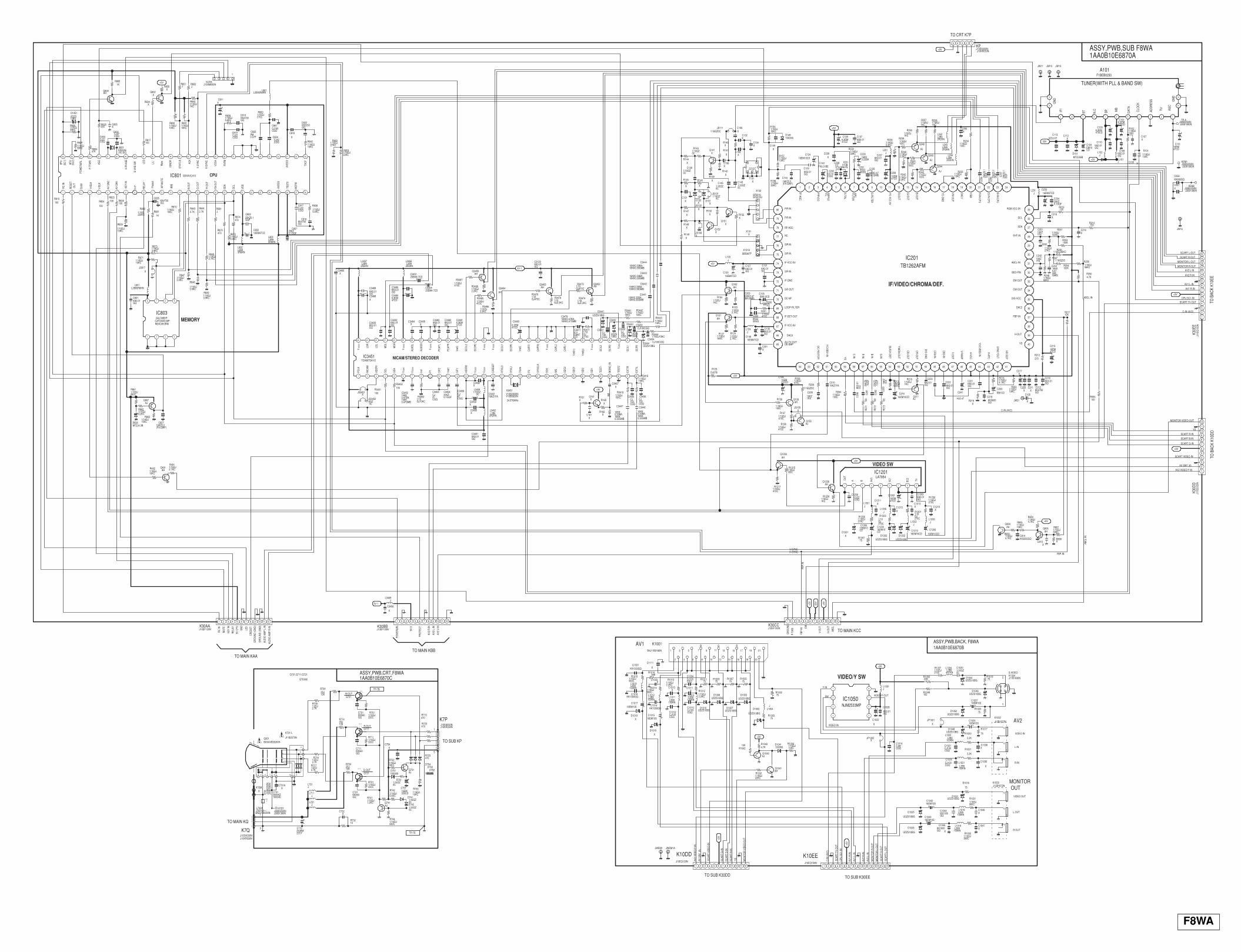
F8WATVSC
1
SC2
AV3
A BOUT
ABCL IN
ASSY,PWB,SUB F8WA1AA0B10E6870A
24.576MHz
AM
GND
GND
IF1
BT N.C
BP MB
DATA
CLO
CK
ADDR
ESS
TU AGC
TUNER(WITH PLL & BAND SW)
1
SCL
SDA
EHT-IN
ABCL-IN
EW-OUT
CW-OUT
DIG-VCC
DAC2
FBP-IN
H-OUT
VD
HD-SCP
H-AFC
Y3/CVBS3-IN
H-VCC
V-RAMP
V-OUT
CB3-IN
CR3-IN
DIG-G
ND
CR-OUT
CB-OUT
Y/MO
N-OUT
BLACK-DET
G-IN
B-IN
R-IN
C-INYS
Y/CVBS1-IN
DC-RESTOR
AU-TV-OUTDE-EMP
IF-VCC-9V
IF-DET-OUT
LOOP-FILTER
DC-NF
SIF-OUT
IF-GND
SIF-IN
IF-VCC-5V
SIF-IN
SIF-IN
NC
PIF-IN
PIF-IN
IF-AGC
PIFVCO
RIPPLEFIL
X-TAL
APCFILTER
S-FILTER
DAC1
YC-VCC-5V
R-OUT
G-O
UT
B-OUT
YC-GND
VM-O
UT
YSM
R-IN-CPU
G-IN-CPU
B-IN-CPU
RGB-VCC-9V
DAC3
BED-PIN
RF-AGC
SYNC^OUT
AVDD
3
TEST
0
MCF
M
TXCF
AVDD
2
PXFM
VDDA
H-SY
NC
V-SY
NC
FB-O
UT
R-O
UT
G-O
UT
B-O
UT
RESE
TO
UT
POW
ER&R
L
KEY
IN
LED
RC IN
8Pin
(SC1
)
8Pin
(SC2
)
Prot
ect
AGC
STAT
US ACK
L/L'
AV S
W1
AV S
W2
S-VH
S SW
BBE
HP-M
UTE
IGNO
R
Mut
e
H-PH
ASE
SCL
SDA
50/6
0
VDD
H-P
H-BL
K
V-BL
K
P-TT
ARI
RELA
Y
RC IN
KEY
IN
RELA
Y
LED
GRO
UND
(GND
)
AV3
R-IN
AV3
L-IN
5V C
PU
AV3
V-IN
GRO
UND
(GND
)
ABCL
IN
5V-0
GND
G-OUT
R-OUT
B-OUT
5
1
TP-7B
TP-7E
1
3
Q701,Q711,Q721 ASSY,PWB,CRT,F8WA1AA0B10E6870C
ASSY,PWB,BACK, F8WA1AA0B10E6870B
1
2
3
4
5
6
7
8
9
10
11
12
13
14
15
16
17
18
19
20
21
B G R
R-IN
L-IN
R-OUT
L-OUT
Y
VIDEO IN
VIDEO OUT
MONITOROUT
AV2
AV1
L1206
C1204
R1201R1203R1206
L1205 C1215C1212
L1202
C1211L1201
C1200
R1230
C1218
C1205C1213
D1203 D1202
IC1201
Q1202
R1217
R1215
Q807
C827D826
R863
R861
R862
C110
C109
TP-A
C101
C102
C103
C104
R101
R102
L102
L101
C106
D101
C131
R143
R149
R140
R144C136
R142C138
R141
R139
Q141
KP
R809
IC803
C801
R152
Q151
R150
Q152
R147
R148
Q161R161
R162
Q802
R835
R145 R146
C149
R154
C132
C133
C134
T131
C1203C1202
IC3451
X3451
C3459
C3460 L3452
R3453
C3453 C3454 C3458
R3452
R3451
C3480
C3477 R3471
C3476C3481
C3485
C3484
L3456L3457
C3488
C3489
PCLK
NICA
M
ADDR
1
SCL
SDA
V
LOR
LOL
MO
L
MO
R
V AUXO
L
AUXO
R
PCAP
L
PCAP
R
Vref
3
SCO
L2
SCO
R2
SIF2
Vref
1
SIF1
ADDR
2
DDA3
SSA1
VDD
D2
VDD
A1
DDD1
V
VDD
A3
Iref
VSS
D1
P1
VSS
A4
SCO
L1
SCO
R1
Vref
2
CAPR
1
CRES
ET
XTAL
O
XTAL
I
Vtun
e
P2
VSS
D2
SYSC
LK
SCK
WS
SDO
2
SDO
1
SDI2
CAPR
2
CAPL
2
CAPL
1
Vref
(n)
Vref
(p)SS
A2V V
DDA2
SSG
V
SDI1
TEST
1
MO
NO_I
N
TEST
2
EXTI
R
EXTI
L
SCIL
2
SCIR
2
SCIL
1
SCIR
1
R3474
Q3452Q3453
R3476
R3473
R3475
C3482C3483
L3459
C3490
C3493C3492
R3487
R3485
R3486
R3488
Q3455
Q3454
C3467
C3452
C3462
R1226
Q1206
A101
D3441
D3442
D3443
D3444
C3446C3447
C056
C057 KEM2
C107
C108
JS108
R3415
R3416
R3444
R3442R3441
C3434
C3433C3432C3431
C3435 C3436
C112
JW11 JW12 JW13
D131D132
R464C3461
JS131
JS132
X131A
X132
IC201
X231
C232
C140
C124
C231
R230
C230
C208
C207
R238
R240
R242
Q244
Q243
Q242
R256
R257 R258
R234
C235
C236
C237
R215
R214
C234
C233
R202
R251
R254
R248
R255
R212
C213
C217
C218
R246
R253
R216
C219
C220C241
R213
C216
C263
C262
C261
C206
R209
C209
C201
C135
C146
L124
Q121
R124R127
R201
C202
C203 C125
R163
R164
Q162
C121
L103
C120
C127
X131
R243
R241
R239
R158
R157
L201
R264
JS105
Q153
R153C128
R138
R137
R136 Q133
L231
R250
JS111
R123
C251
C242
C126
C144
C223C222 C221
Q211
R218
R263
C210
C215
C214
R165
C123
C212
C113
R219
R233
R247
L244
C243
JS3451
JS3452
C238
C143
C1206
C105
JW21
C239
C161
C225 C211
C256
R200
D149C824
C826
L803
R838C817
C816
C807
R842
C822
C810
C811
R839 C818
C819
R815
R831
R845
R844R843
X801
C834
C833
R808
R880
R872
R875
R874
R832R830
R849
R847
R881
IC801
R848
R826
C835
C802
C803
R840
C823
R824R823
R870
C861
R860D1051
R851
R817
Q808
R884
R834
R3443
K30D
D
K30BB K30CC
JS617
L801
R873
K30AA
L861
Q805
Q804
R858
R857
R854
C815
C814
R855
R856
KCPAR822R821
R885
L242
EW
Q491R492R491
R217
FBP-
IN
R853
R852
H-SYNC
FBP-
IN
H-O
UT
ABCL
V-O
UT
AV2 L-IN
AV2 R-IN
AV1 L-IN
AV1 R-IN
C-IN (AV2)
SCART G-IN
SCART B-IN
SCART R-IN
YS
SCART VIDEO-IN
AV2 VIDEO/Y-IN
CPU SC1-IN
MONITOR L-OUT
MONITOR R-OUT
MONITOR VIDEO-OUT
SCART L-OUT
SCART R-OUT
P-TA
RI
MUT
E
AUDI
O A
MP
L-IN
AUDI
O A
MP
R-IN
PRO
TECT
CRES
ET
POW
ER&R
L
AV SW1 (A)
SCART TV-OUT
GRO
UND
R1207
R871
JW16
C3409
C3401
FBP-IN
C-IN (AV2)
C145
L3469
C3456
V-SYNC
L243
K30E
E
C3495C3494
KEM1
C3129
C137C139
L802
R829
C3441
C3443
C3442
C3444
C3491
D1201
R271
R272
R273
AT1
Q721
R724
Q711
R714
Q701
R705
R732
K701-L
C731K7M
R704
K7P
K7Q
C732
L701
R703
R713
R723
R701C701
C711
R711
R721
C721
R741
Q741
R742
R744
L702
D742
D741
R753C751
D751
R752
R751
D754D753
D752Q751Q721A
Q711A
Q701A
R717
R716
K7D1L702A
C754
C731A
C710
K7EM
L711
L721
Q901
R1011
K10DD
C1031
R1002
D1002
R1003
R1005
D1007
R1007R1009
D1008
D1010
R1012
L1010
C1010
C1012
L1011
R1013
C1015
R1014
L1012
C1014
C1016
L1013
R1015
C1017
K1001
D1003
R1016
R1042
Q1042
Q1041
R1043
R1041
C1033C1034
C1111
D1041
D1018
D1019
R1034
C1013 C1011
L1004D1052
D1046
R1050
R1023
R1017
D1021
R1018
R1019
C1021
L1020 R1020
R1021
L1021C1024
D1025
D1026
C1036
C1038
D1044
C1043
R1032
L1019 C1047
C1042
L1018
R1031
C1046C1044
C1045
C
S-VIDEO
AV1
R-IN
AV1
L-IN
AV2
R-IN
AV2
L-IN
AV2
VIDE
O/Y
-IN
MO
NITO
R VI
DEO
-OUT
MO
NITO
R R-
OUT
MO
NITO
R L-
OUT
C-IN
(AV2
)
SCAR
T TV
-OUT
SCAR
T R-
IN
SCAR
T B-
IN
SCAR
T G
-IN
SCAR
T VI
DEO
-IN
SCAR
T L-
OUT
SCAR
T R-
OUT
AV S
W1
(A)
YS CPU
SC1-
IN
IC1050R1048
D1048
L1204R1227 C1020
C1214
C1028
K1002
K1003
K1004
C1037
C1023
K10EE
C1022
L1051
JP1002
JP1001
JWEM1 JWEM1A
J
16EM10CD
1/16GJ270C1/16
GJ270C
1/16GJ270C
J X
X
J
XJ
16EM10CD
1/16GJ270C
X
16EM10CD16EM10CD
UDZS10BG UDZS10BG
LA7954
AH
1/16GJ470C
1/16GJ100C
AJ
16KZ2.2(FA:GWF)
MTZJ4.3B
1/16GJ15KC
1/16GJ680C
1/16GJ8.2KC
KK0.01GQ
KK0.01GQ
J30B0250N:J30B1380N
16EM47CD
6.3EM470CD
6.3EM470CD
EM10CD
1/16GJ100C
1/16GJ100C
J
J
X
MTZJ36B
X
1/16GZ0C
X
X
XX
X
1/16GZ0C
X
X
X
J10EA050N:J10KR050N
1/16GJ10KC
24LC08B/P: CAT24WC08P:M24C08-BN6
KK0.01GQ
X
X
X
X
X
X
XX
X
X
X
X X
X
1/16GJ10KC
X
X
X
X
KK0.01GQ16EM
47CD
TDA9875A/V2
V10B2830N:V10B5820N
X
X L2B92R2KN
1/16GJ10KC
CJ47CGQ
25KZ0.1GQF
CJ47CGQ
100
100
6.3EM47CD
6.3EM47CD
1/16GJ270C
16KK0.47BA:16KK0.47GMB6.3EM
47CD
KK0.01GQ
6.3EM47CD
L2B92R2KN
L2B92R2KN
X
KK0.01GQ
1/16GJ2.2KC
AHAH
1/16GJ2.2KC
1/16GJ470C
1/16GJ470C
KK0.01GQ
KK0.01GQ
1/16GZ0C
X
KK0.01GQ
KK0.01GQ
1/16GJ470C
1/16GJ470C
1/16GJ2.2KC
1/16GJ2.2KC
AH
AH
X
16KK0.47BA:16KK0.47GMB
X
1/16GJ1KC
AH
F1BEB0250
UDZS10BG
UDZS10BG
UDZS10BG
UDZS10BG
16KK0.33BA:16KK0.33GMB
16KK0.33BA:16KK0.33GMB
KK680GQ
X J30B0250N:J30B1380N
X
X
X
1/16GJ15KC
1/16GJ15KC
1/16GJ15KC
1/16GJ15KC
1/16GJ15KC
CJ100CGQ
CJ100CGQCJ100CGQ
CJ100CGQ
CJ100CGQ
CJ100CGQ
X
X X X
XX
10016KZ1FA
1/16GZ0C
X
SB5387P
SF5315:SF5315U
TB1262AFM
V10B 2961N
CC10CGQ
FK0.01BE
16EM10CD
KK2200GQ
1/16GJ33KC
16KK0.22BA
16EM47CD
KK0.01GQ
1/16GJ2.2KC
1/16GJ2.2KC
1/16GJ2.2KC
AJ
AJ
AJ
1/16GJ1KC
1/16GJ1KC
1/16GJ1KC
1/16GJ100C
25KZ
0.1
GQ
F
25KZ
0.1
GQ
F
25KZ
0.1
GQ
F
100
100
25KZ0.1GQF
16EM47CD
1/16GJ27KC
1/16GJ120KC
100K
1/16GJ82KC
1/16GJ56KC
270
16EM47CD
X
KK0.01GQ
1/16GJ39KC
100K
1/16GJ4.7KC
KK5600GQ
EM1CD
HJ0.47
1/16GJ100KC
16EM10CD
16KZ
1FA
25KZ
0.1
GQ
F
25KZ
0.1
GQ
F
KK0.
01G
Q
1/16GZ0C
16KZ1FA
X
KK0.01GQ
16EM47CD
J
AH
1/16GJ2.7KC
1/16GJ560C
1/16GJ470C
KK2200GQ
16KK0.47(BA:GMB)
EM2.2CD
1/16GJ2.7KC
1/16GJ1KC
AH
KK0.01GQ
J
16EM47CD
KK0.01GQ
X
1/16GJ100C
1/16GJ100C
1/16GJ100C
1/16GJ39KC
1/16GJ10KC
J
1/16GJ100C
X
AJ
1/16GJ470C
10EM220CD
1/16GJ470C
1/16GJ470C
1/16GJ100C
AH
J
4.7K
1/16GZ0C
DJ27B
16KZ1FA
16KZ1FA
16KK0.47(BA:GMB)
16KZ2.2(FA:GWF)
KK0.01GQ KK0.01
GQKK0.01GQ
AJ
1/16GJ1KC
1/16GJ10KC
16KZ1FA
X
X
X
KK0.01GQ
KK2700GQ
KZ0.01F
X
1/16GJ10KC
1/16GZ0C
L2B92R2KN
16KK0.47(BA:GMB)
X
1/16GZ0C
CC1CGQ
1/16GZ0C
CJ22CGQ
X
X
X
X
X X
X
X
1SS355CJ82CGQ
PM0.47P
L2B95R6KN
1/16GJ5.6KC
CJ22CGQ
KK4700GQ
25KZ0.1GQF
1/16GJ15KC
KK2200GQ
X
X
1/16GJ5.6KC
KK4700GQ
CJ22CGQ
100
1/16GJ10KC
1/16GJ2.7KC
2.7K2.7K
EX0046(XC:SC)
CJ27CGQ
CJ27CGQ
100
1/16GJ39KC
1/16GJ3.9KC
470
470
1/16GJ10KC1/16GJ
33KC
1/16GJ3.9KC
1/16GJ3.9KC
1K
QXXAVC410
1/16GJ3.9KC
220
KK4700GQ
10EM47CD
25KZ0.1GQF
1/16GJ1KC
X
100
100
1/16GJ100C
CJ150CGQ
1/16GJ270CUDZS
10BG
J
100
AH
47K
X
1/16GJ15KC
J11E
G12
0N
J10EF120N J10EF120N
X
L2B95R6KN
1/16GJ3.9KC
J10EF120N
L2B95R6KN
AH
AH
X
1/16GJ33KC
1/16GJ4.7KC
X
KK3300GQ
1/16GJ10KC
1/16GJ4.7KC
J10AM050NJJ
1K
L2B92R2KN
AH1/16GJ10KC
1/16GJ2.7KC
10K
1/16GJ22KC
1/16GJ27KC
1
75
1/16GJ10KC
X
25EM4.7CD
25EM4.7CD
1/16GZ0C
J
X
L2B92R2KN
J11E
G15
0N
XX
J30B0250N:J30B1380N
KK0.01GQ
KK0.01GQ
6.3EM47CD
L2B95R6KN
1/16GJ33KC
16KK0.33BA:16KK0.33GMB
16KK0.33BA:16KK0.33GMB
16KK0.33BA:16KK0.33GMB
16KK0.33BA:16KK0.33GMB
KK0.01GQ
X
100
100
100
2SJ12K
2SJ12K
QT0392
1/2DJ2.7K
10
J11B2570N
2000KZ1000HE
J30B
0250
N:J3
0B13
80N
2SJ12K
J10EA050N:J10KR050N
J10EA030N:J10KR030N
X
J
470
470
470
1/16GJ220C
KK560GQ
KK560GQ
1/16GJ220C
1/16GJ220C
KK560GQ
1/16GJ1.2KC
AJ
1/16GJ5.6KC
1/16GJ680C
X
1/16GZ0C
1/16GZ0C
1/16GJ10KC
16EM330CD
1SS355
1/16GJ10KC
1/16GZ0C
1SS3551SS3551SS355AJX
X
X
1/2DJ2.7K
1/2DJ2.7K
J30B0250N:J30B1380N
Z20103---:B4Z21B0090N
X
X
250EM22CY
X
J
J
BXXAVB352KIH-
75
J10EQ120N
KK1000GQ
75
UDZS10BG
75
75
UDZS10BG
7575
UDZS10BG
UDZS10BG
1/16GJ2.2KCL2B9
100KN
CJ100CGQ
CJ100CGQ
L2B9100KN
1/16GJ2.2KC
16EM10S
1/16GJ560C
L2B9100KN
KK1000GQ
KK1000GQ
L2B9100KN
1/16GJ560C
16EM10S
B4J11B0180N
UDZS10BG
39K
100
AJ
AH
4.7K
1/16GJ22KC
XCJ100CGQ
X
1SS355
X
X
1/16GJ10KC
X X
J
UDZS10BG
UDZS10BG
22K
75
75
UDZS10BG
75
75
CJ100CGQ
L2B9100KN
2.2K
2.2K
L2B9100KN
CJ100CGQ
UDZS10BG
UDZS10BG
X
X
UDZS10BG
16EM10S
1/16GJ560C
L2B9100KN
X
16EM10S
L2B9100KN
1/16GJ560C
XKK1000GQ
KK1000GQ X
NJM2533MP
VIDEO/Y-OUT 100
Y-IN
SW
UDZS10BG
VIDEO-IN
L2B94R7KN
1/16GJ270C
1/16GZ0C
CJ82CGQ
KK0.01GQ
J12B1972N
J12B1972N
J11B1630N
16EM10S
16EM10S
J10EQ150N
X
J
X
X
1 2 3 4 5 6 7 8 9
12345
1 2 3 4
5678
1 2 3 4 5 6 7 8 9 10 11 12 13 14 15 16 17 18 19 20 21 22 23 24 25 26 27 28 29 30 31 32
3334353637383940414243444546474849505152535455565758596061626364
1234567891011
12
13 14
15
1 2 3 4 5 6 7 8 9 10 11 12 13 14 15 16 17 18 19 20 21 22 23 24
25
26
27
28
29
30
31
32
33
34
35
36
37
38
39
40
414243444546474849505152535455565758596061626364
65
66
67
68
69
70
71
72
73
74
75
76
77
78
79
80
1 2 3 4 5 6 7 8 9 10 11 12 13 14 15 16 17 18 19 20 21 22 23 24 25 26 27 28
29303132333435363738394041424344454647484950515253545556
1
2
3
4
5
6
7
8
9
10
11
12
1 2 3 4 5 6 7 8 9 10 11 12 1 2 3 4 5 6 7 8 9 10 11 121 2 3 4 5 6 7 8 9 10 11 12
1
2
3
4
5
6
7
8
9
10
11
12
13
14
15
2 7 5 10 9
8
6
11
-41
121110987654321
1
2
3
4 5
6
7
8
1 2 3 4 5 6 7 8 9 10 11 12 13 14 15
+9V
+5V
+9V
+5V
+9V
5V-1
+5V
+9V
+5V
+9V
+9V
+5V
5V-1 +9V
33V
33V
+5V
+9V
+5V
+5V
+9V
TO MAIN KCC
TO MAIN KBBTO MAIN KAA
VIDEO SW
IF/VIDEO/CHROMA/DEF.
NICAM/STEREO DECODER
CPU
MEMORY
VIDEO/Y SW
TO SUB K30EETO SUB K30DD
TO B
ACK
K10E
ETO
BAC
K K1
0DD
TO CRT K7P
TO SUB KP
TO MAIN KQ
Related Documents