TUTORIAL

Welcome message from author
This document is posted to help you gain knowledge. Please leave a comment to let me know what you think about it! Share it to your friends and learn new things together.
Transcript
TUTORIAL
DipTrace Tutorial2
© 2011 Novarm Ltd.
Table of Contents
Part I Introduction 4
Part II Creating a simple Schematic and PCB 4
................................................................................................................................... 51 Establishing a schematic size and placing titles
................................................................................................................................... 82 Configuring libraries
................................................................................................................................... 103 Designing a schematic
................................................................................................................................... 284 Converting to a PCB
................................................................................................................................... 315 Designing a PCB
.......................................................................................................................................................... 31Preparing to route
.......................................................................................................................................................... 36Autorouting
.......................................................................................................................................................... 39Working with layers
.......................................................................................................................................................... 42Working with vias
.......................................................................................................................................................... 45Net Classes
.......................................................................................................................................................... 48Manual Routing
.......................................................................................................................................................... 53Measuring trace length
.......................................................................................................................................................... 55Selecting objects by type/layer
.......................................................................................................................................................... 59Placing Text and Graphics
.......................................................................................................................................................... 62Copper Pour
.......................................................................................................................................................... 67Locking objects
.......................................................................................................................................................... 69Design Verification
.......................................................................................................................................................... 72Design Information
.......................................................................................................................................................... 73Panelizing
.......................................................................................................................................................... 77Printing
................................................................................................................................... 796 Manufacturing Output
.......................................................................................................................................................... 79DXF Output
.......................................................................................................................................................... 81Gerber Output
.......................................................................................................................................................... 87Create NC Drill file for CNC machine drilling
Part III Creating Libraries 88
................................................................................................................................... 881 Designing a pattern library
.......................................................................................................................................................... 88Customizing Pattern Editor
.......................................................................................................................................................... 89Designing a resistor (pattern)
.......................................................................................................................................................... 98Saving library
.......................................................................................................................................................... 99Designing BGA-144/12x12
.......................................................................................................................................................... 105Designing SOIC-28 pattern
.......................................................................................................................................................... 108Placing patterns
................................................................................................................................... 1112 Designing a component library
.......................................................................................................................................................... 111Customizing Component Editor
.......................................................................................................................................................... 113Designing a resistor (component)
.......................................................................................................................................................... 117Designing a capacitor
.......................................................................................................................................................... 125Designing a multi-part component
.......................................................................................................................................................... 134Designing PIC18F24K20
.......................................................................................................................................................... 144Designing VCC and GND symbols
.......................................................................................................................................................... 147Using additional fields
.......................................................................................................................................................... 151Spice settings
.......................................................................................................................................................... 152Library Verification
.......................................................................................................................................................... 154Placing parts

3Contents
© 2011 Novarm Ltd.
Part IV Using different package features 159
................................................................................................................................... 1601 Connecting
.......................................................................................................................................................... 160Working with Buses and Bus Connectors
.......................................................................................................................................................... 165Working with Net Ports
.......................................................................................................................................................... 166Connecting without wires
.......................................................................................................................................................... 170Connection Manager in Schematic and PCB Layout
................................................................................................................................... 1712 Reference Designators
................................................................................................................................... 1783 How to find components in libraries
................................................................................................................................... 1794 Electrical Rule Check
................................................................................................................................... 1815 Bill of Materials (BOM)
................................................................................................................................... 1846 Importing/Exporting netlists
................................................................................................................................... 1877 Saving/Loading Design Rules
................................................................................................................................... 1888 Spice simulation
................................................................................................................................... 1929 Checking net connectivity
................................................................................................................................... 19510 Placement features
................................................................................................................................... 20211 Fanout
................................................................................................................................... 20712 Hierarchical Schematic
................................................................................................................................... 21413 3D View
Part V DipTrace Links 218
DipTrace Tutorial4
© 2011 Novarm Ltd.
1 Introduction
This document allows you to easily get started with DipTrace by designing simple Schematicand its PCB, pattern and component libraries, then trying different package features. Tutorialincludes step-by-step design guide and many additional insets, that allow you to discoverprogram features. If you have any questions while learning the tutorial, contact our supportstaff: [email protected]. We will be happy to assist and gladly answer all your questions.This tutorial was created for DipTrace ver. 2.2.0.0 (build September 7, 2011)
2 Creating a simple Schematic and PCB
This part of tutorial will teach you, how to create a simple schematic and its PCB (PrintedCircuit Board) using DipTrace program.
You will be creating this schematic, using DipTrace schematic capture module: OpenDipTrace Schematic Capture module, i.e., go to Start All Programs DipTrace Schematic.
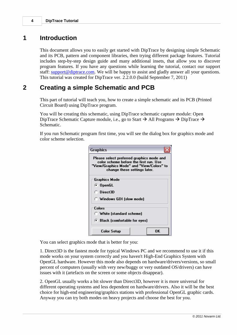
If you run Schematic program first time, you will see the dialog box for graphics mode andcolor scheme selection.
You can select graphics mode that is better for you:
1. Direct3D is the fastest mode for typical Windows PC and we recommend to use it if thismode works on your system correctly and you haven't High-End Graphics System withOpenGL hardware. However this mode also depends on hardware/drivers/versions, so smallpercent of computers (usually with very new/buggy or very outdated OS/drivers) can haveissues with it (artefacts on the screen or some objects disappear).
2. OpenGL usually works a bit slower than Direct3D, however it is more universal fordifferent operating systems and less dependent on hardware/drivers. Also it will be the bestchoice for high-end engineering/graphics stations with professional OpenGL graphic cards.Anyway you can try both modes on heavy projects and choose the best for you.
Creating a simple Schematic and PCB 5
© 2011 Novarm Ltd.
3. Windows GDI can be used as alternate mode if both Direct3D and OpenGL don't workcorrectly with your graphics card. It is much slower but doesn't depend on drivers/hardware/OS. Also this mode is enough for comfortable work on small and medium-sized projects.
We will use white background as more acceptable for printing this tutorial, you can select thecolor scheme you want. Also notice that you can change color scheme or define colors youwant any time from "View / Colors".
The same dialog box will appear in PCB Layout module. Component Editor and PatternEditor use color settings of Schematic Capture and PCB Layout accordingly.
Also we will sometimes hide Design manager / Properties panel on the right side to add moredesign space. But if you have a high resolution and don't have a lack of free space, you canleave it. Select "View / Toolbars / Design Manager" from main menu.
2.1 Establishing a schematic size and placing titles
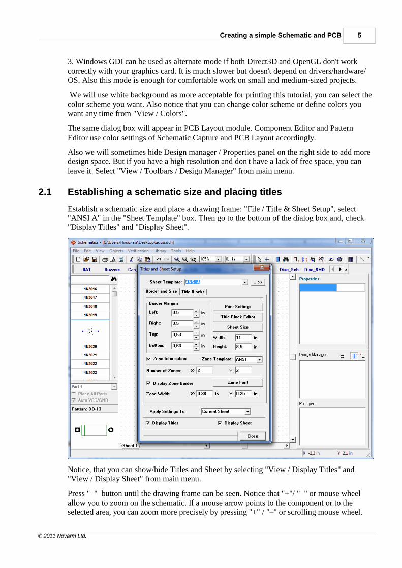
Establish a schematic size and place a drawing frame: "File / Title & Sheet Setup", select "ANSI A" in the "Sheet Template" box. Then go to the bottom of the dialog box and, check"Display Titles" and "Display Sheet".
Notice, that you can show/hide Titles and Sheet by selecting "View / Display Titles" and"View / Display Sheet" from main menu.
Press "–" button until the drawing frame can be seen. Notice that "+"/ "–" or mouse wheelallow you to zoom on the schematic. If a mouse arrow points to the component or to theselected area, you can zoom more precisely by pressing "+" / "–" or scrolling mouse wheel.
DipTrace Tutorial6
© 2011 Novarm Ltd.
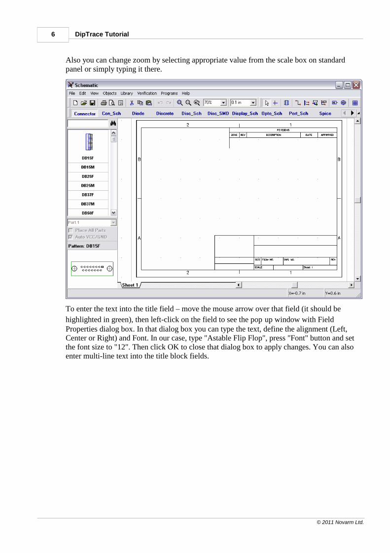
Also you can change zoom by selecting appropriate value from the scale box on standardpanel or simply typing it there.
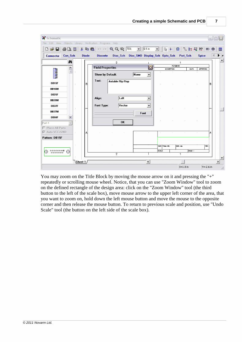
To enter the text into the title field – move the mouse arrow over that field (it should be
highlighted in green), then left-click on the field to see the pop up window with FieldProperties dialog box. In that dialog box you can type the text, define the alignment (Left,Center or Right) and Font. In our case, type "Astable Flip Flop", press "Font" button and setthe font size to "12". Then click OK to close that dialog box to apply changes. You can alsoenter multi-line text into the title block fields.
Creating a simple Schematic and PCB 7
© 2011 Novarm Ltd.
You may zoom on the Title Block by moving the mouse arrow on it and pressing the "+"repeatedly or scrolling mouse wheel. Notice, that you can use "Zoom Window" tool to zoomon the defined rectangle of the design area: click on the "Zoom Window" tool (the thirdbutton to the left of the scale box), move mouse arrow to the upper left corner of the area, thatyou want to zoom on, hold down the left mouse button and move the mouse to the oppositecorner and then release the mouse button. To return to previous scale and position, use "UndoScale" tool (the button on the left side of the scale box).
DipTrace Tutorial8
© 2011 Novarm Ltd.
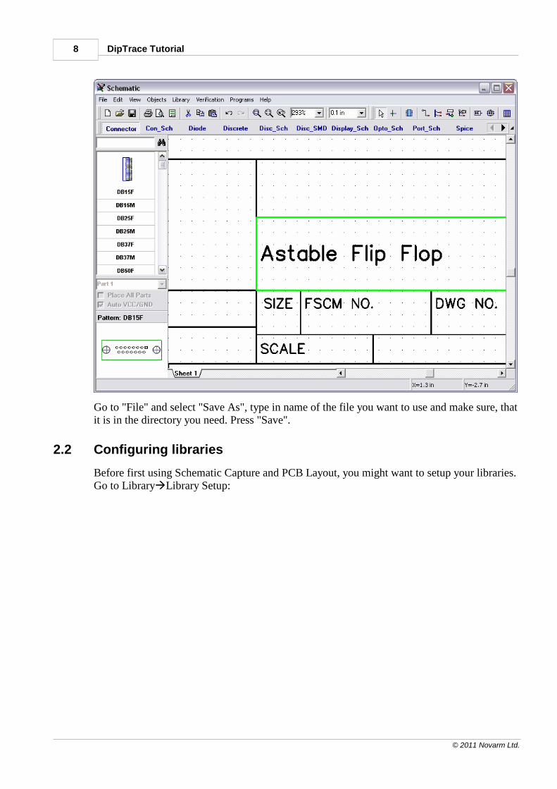
Go to "File" and select "Save As", type in name of the file you want to use and make sure, thatit is in the directory you need. Press "Save".
2.2 Configuring libraries
Before first using Schematic Capture and PCB Layout, you might want to setup your libraries.Go to Library Library Setup:
Creating a simple Schematic and PCB 9
© 2011 Novarm Ltd.
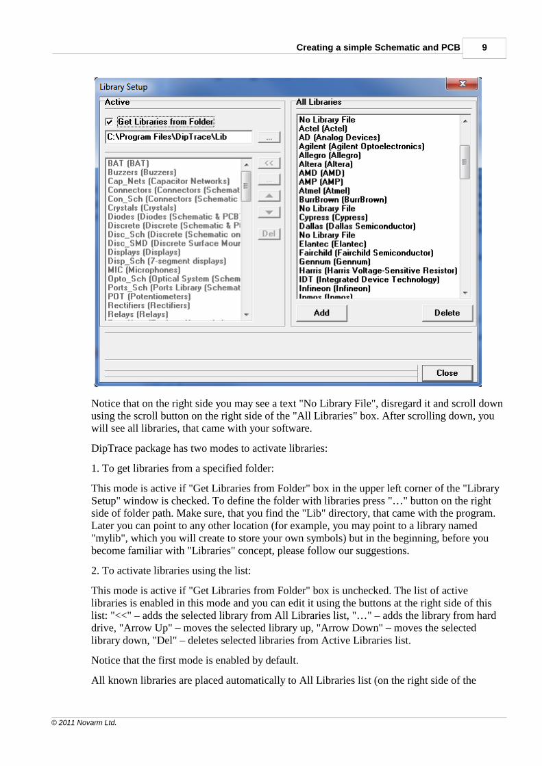
Notice that on the right side you may see a text "No Library File", disregard it and scroll downusing the scroll button on the right side of the "All Libraries" box. After scrolling down, youwill see all libraries, that came with your software.
DipTrace package has two modes to activate libraries:
1. To get libraries from a specified folder:
This mode is active if "Get Libraries from Folder" box in the upper left corner of the "LibrarySetup" window is checked. To define the folder with libraries press "…" button on the rightside of folder path. Make sure, that you find the "Lib" directory, that came with the program.Later you can point to any other location (for example, you may point to a library named"mylib", which you will create to store your own symbols) but in the beginning, before youbecome familiar with "Libraries" concept, please follow our suggestions.
2. To activate libraries using the list:
This mode is active if "Get Libraries from Folder" box is unchecked. The list of activelibraries is enabled in this mode and you can edit it using the buttons at the right side of thislist: "<<" – adds the selected library from All Libraries list, "…" – adds the library from harddrive, "Arrow Up" – moves the selected library up, "Arrow Down" – moves the selectedlibrary down, "Del" – deletes selected libraries from Active Libraries list.
Notice that the first mode is enabled by default.
All known libraries are placed automatically to All Libraries list (on the right side of the
DipTrace Tutorial10
© 2011 Novarm Ltd.
dialog box). Also you can add or delete libraries from that list using "Add" or "Delete"buttons.
Close the Library Setup dialog box and all changes, if made, will be applied to the Librariespanel.
If you want to move components from a design to a library, select these components, move amouse arrow over one of them, right-click, then select "Save to Library". From the "Save toLibrary" submenu you can add the selected component to active library (shown on the leftside of screen) or save them to a different library.
2.3 Designing a schematic
Now, please, change grid size to 0.1 in. you can select it from the list of grids (combo boxwith "0.05 in" text), or press "Ctrl+" to increase grid size, to reduce it – press "Ctrl-". Hotkeys work only if current grid size is listed in available grids. To change list of grids select"View / Customize Grid" from main menu.
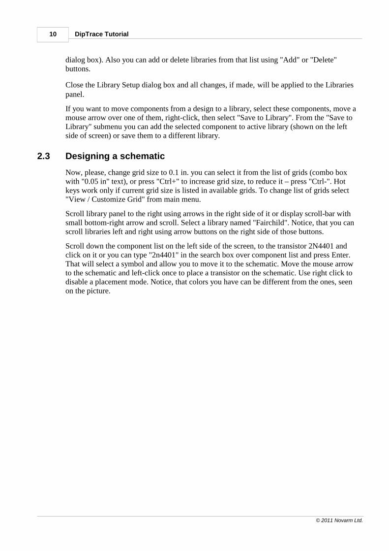
Scroll library panel to the right using arrows in the right side of it or display scroll-bar withsmall bottom-right arrow and scroll. Select a library named "Fairchild". Notice, that you canscroll libraries left and right using arrow buttons on the right side of those buttons.
Scroll down the component list on the left side of the screen, to the transistor 2N4401 andclick on it or you can type "2n4401" in the search box over component list and press Enter.That will select a symbol and allow you to move it to the schematic. Move the mouse arrowto the schematic and left-click once to place a transistor on the schematic. Use right click todisable a placement mode. Notice, that colors you have can be different from the ones, seenon the picture.
Creating a simple Schematic and PCB 11
© 2011 Novarm Ltd.
How to move a symbol around? Hold down the left mouse button on the symbol and move ituntil you find a proper place for it. If you need to move several symbols you should selectthem first, then drag-and-drop. To select a single symbol, left-click on it. If you want to selectseveral symbols, press and hold down "Ctrl" button and click on each symbol, that you wantto select in your group of symbols. Also you can select the group of symbols using a differentway: move mouse to the upper-left corner of the group, hold down the left mouse button,move cursor to lower-right corner and release the mouse button (if the Ctrl key is pressed, theselection will be inverted).
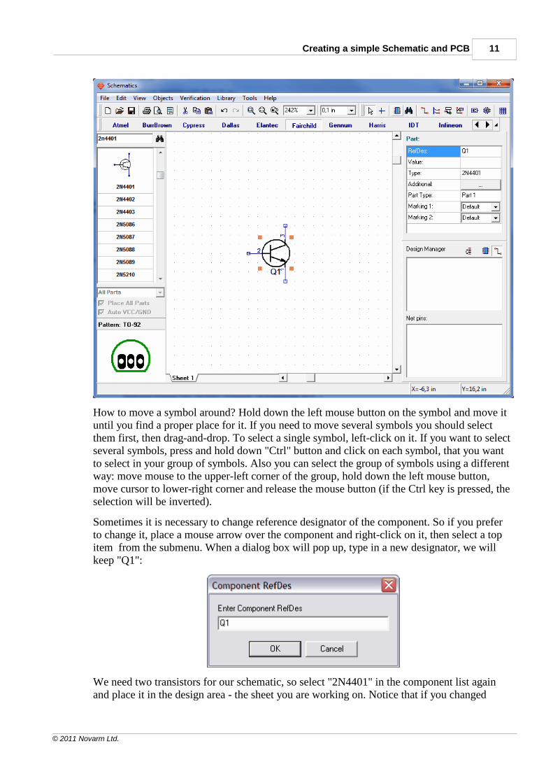
Sometimes it is necessary to change reference designator of the component. So if you preferto change it, place a mouse arrow over the component and right-click on it, then select a topitem from the submenu. When a dialog box will pop up, type in a new designator, we willkeep "Q1":
We need two transistors for our schematic, so select "2N4401" in the component list againand place it in the design area - the sheet you are working on. Notice that if you changed
DipTrace Tutorial12
© 2011 Novarm Ltd.
designator, you don’t need to rename the second transistor, because it is done automatically. Ifyou want to rotate the symbol before placing it on the schematic, press Space Bar or "R"button.
Select a library named "Discrete" on the library panel, find a suitable resistor and place it.
Select RES400, which designates a resistor with 400 mils of lead spacing. By the way, if youprefer a drawing in metric units, select "View / Units / mm" from main menu, however wewill keep inches as this is more suitable for our project. For future we recommend to payattention to active units to avoid mistakes.
Creating a simple Schematic and PCB 13
© 2011 Novarm Ltd.
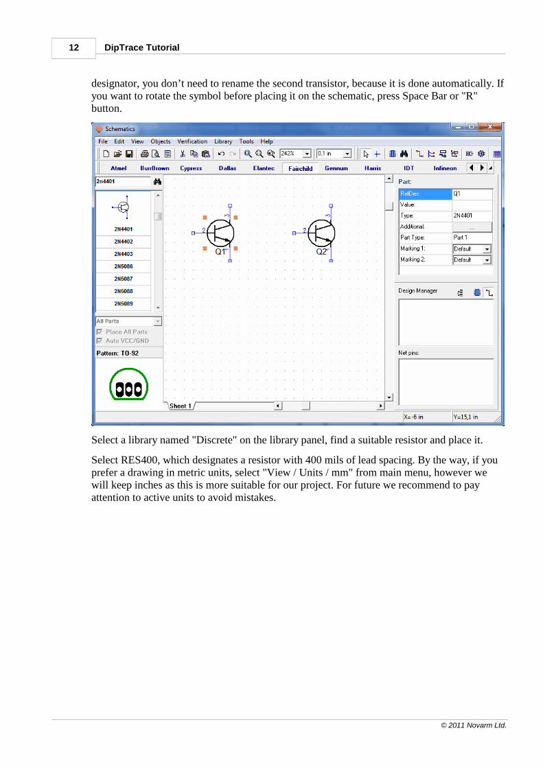
We need 4 resistors on the schematic. Notice that you can simply place them from acomponent panel on the left, the same way you placed the Q1 and Q2, but now we will useanother method. Select your resistor (move mouse over it and left click) and copy it 3 times.you can use 2 ways to copy this symbol:
1. Select "Edit / Copy" from the main menu (or "right click on resistor / Copy" or "Ctrl+C"),then select "Edit / Paste" 3 times or right-click in the position, where you want to place newresistor and "Paste" from pop-up menu, also 3 times.
2. The second method is named "Copy Matrix". Select your resistor, then "Edit / CopyMatrix" from the main menu (or press "Ctrl+M").
In the "Copy Matrix" dialog box set the number of columns and rows ("2" columns and "2"rows to get 4 resistors) and spacing (1 inch for columns and 0.4 inch for rows are suitable),
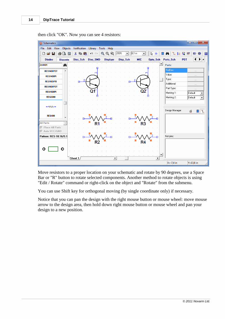
DipTrace Tutorial14
© 2011 Novarm Ltd.
then click "OK". Now you can see 4 resistors:
Move resistors to a proper location on your schematic and rotate by 90 degrees, use a SpaceBar or "R" button to rotate selected components. Another method to rotate objects is using"Edit / Rotate" command or right-click on the object and "Rotate" from the submenu.
You can use Shift key for orthogonal moving (by single coordinate only) if necessary.
Notice that you can pan the design with the right mouse button or mouse wheel: move mousearrow to the design area, then hold down right mouse button or mouse wheel and pan yourdesign to a new position.
Creating a simple Schematic and PCB 15
© 2011 Novarm Ltd.
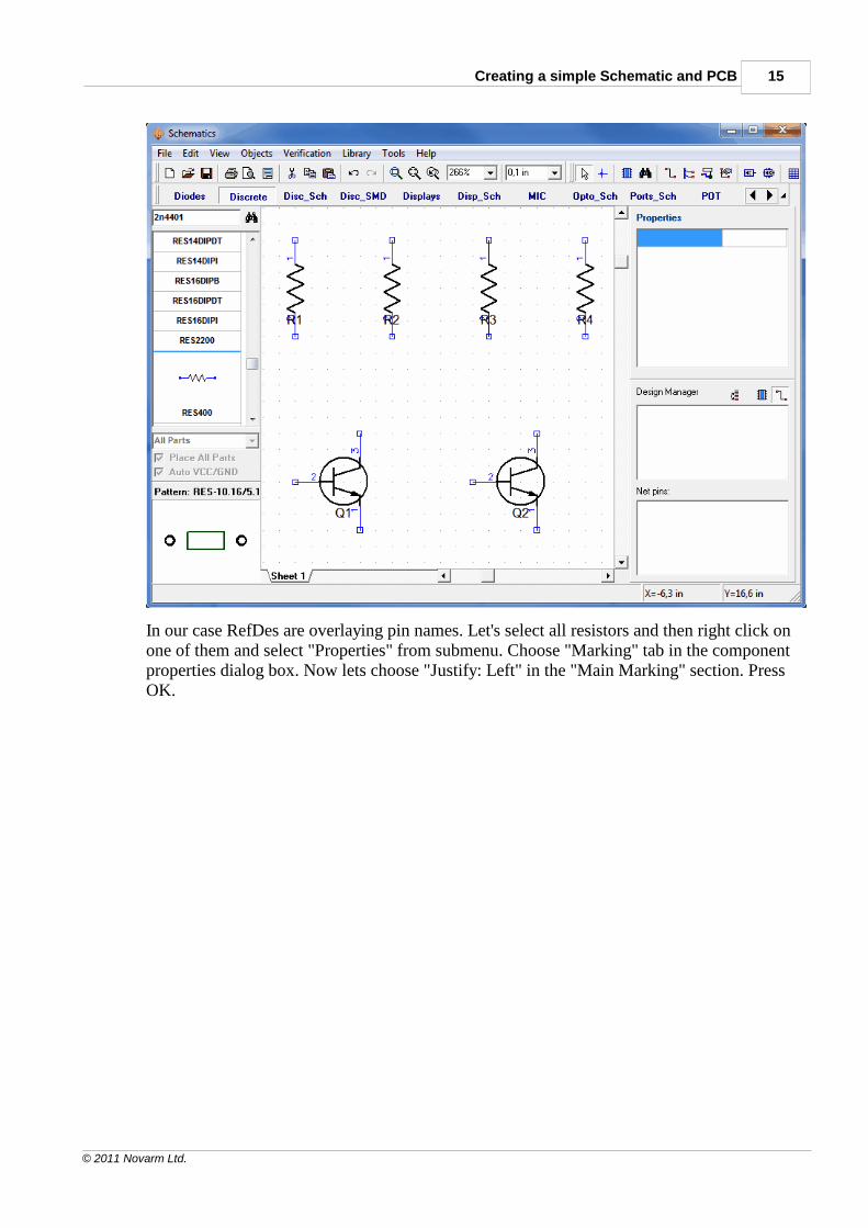
In our case RefDes are overlaying pin names. Let's select all resistors and then right click onone of them and select "Properties" from submenu. Choose "Marking" tab in the componentproperties dialog box. Now lets choose "Justify: Left" in the "Main Marking" section. PressOK.
DipTrace Tutorial16
© 2011 Novarm Ltd.
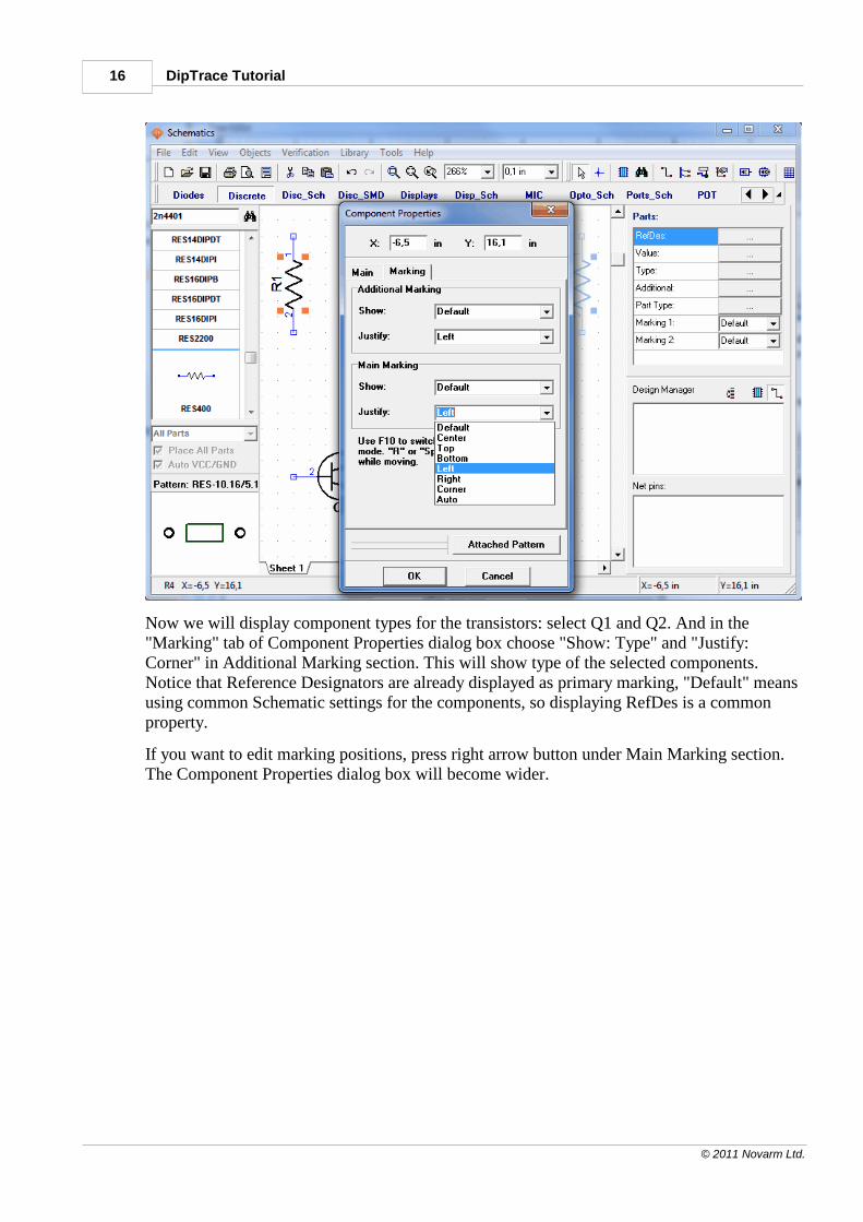
Now we will display component types for the transistors: select Q1 and Q2. And in the"Marking" tab of Component Properties dialog box choose "Show: Type" and "Justify:Corner" in Additional Marking section. This will show type of the selected components.Notice that Reference Designators are already displayed as primary marking, "Default" meansusing common Schematic settings for the components, so displaying RefDes is a commonproperty.
If you want to edit marking positions, press right arrow button under Main Marking section.The Component Properties dialog box will become wider.
Creating a simple Schematic and PCB 17
© 2011 Novarm Ltd.
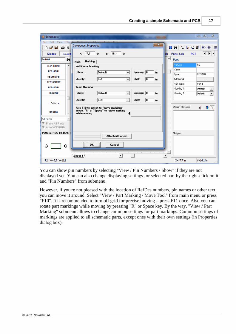
You can show pin numbers by selecting "View / Pin Numbers / Show" if they are notdisplayed yet. You can also change displaying settings for selected part by the right-click on itand "Pin Numbers" from submenu.
However, if you're not pleased with the location of RefDes numbers, pin names or other text,you can move it around. Select "View / Part Marking / Move Tool" from main menu or press"F10". It is recommended to turn off grid for precise moving – press F11 once. Also you canrotate part markings while moving by pressing "R" or Space key. By the way, "View / PartMarking" submenu allows to change common settings for part markings. Common settings ofmarkings are applied to all schematic parts, except ones with their own settings (in Propertiesdialog box).
DipTrace Tutorial18
© 2011 Novarm Ltd.
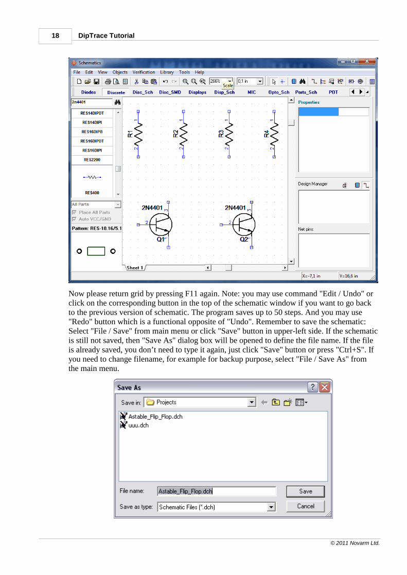
Now please return grid by pressing F11 again. Note: you may use command "Edit / Undo" orclick on the corresponding button in the top of the schematic window if you want to go backto the previous version of schematic. The program saves up to 50 steps. And you may use"Redo" button which is a functional opposite of "Undo". Remember to save the schematic:Select "File / Save" from main menu or click "Save" button in upper-left side. If the schematicis still not saved, then "Save As" dialog box will be opened to define the file name. If the fileis already saved, you don’t need to type it again, just click "Save" button or press "Ctrl+S". Ifyou need to change filename, for example for backup purpose, select "File / Save As" fromthe main menu.
Creating a simple Schematic and PCB 19
© 2011 Novarm Ltd.
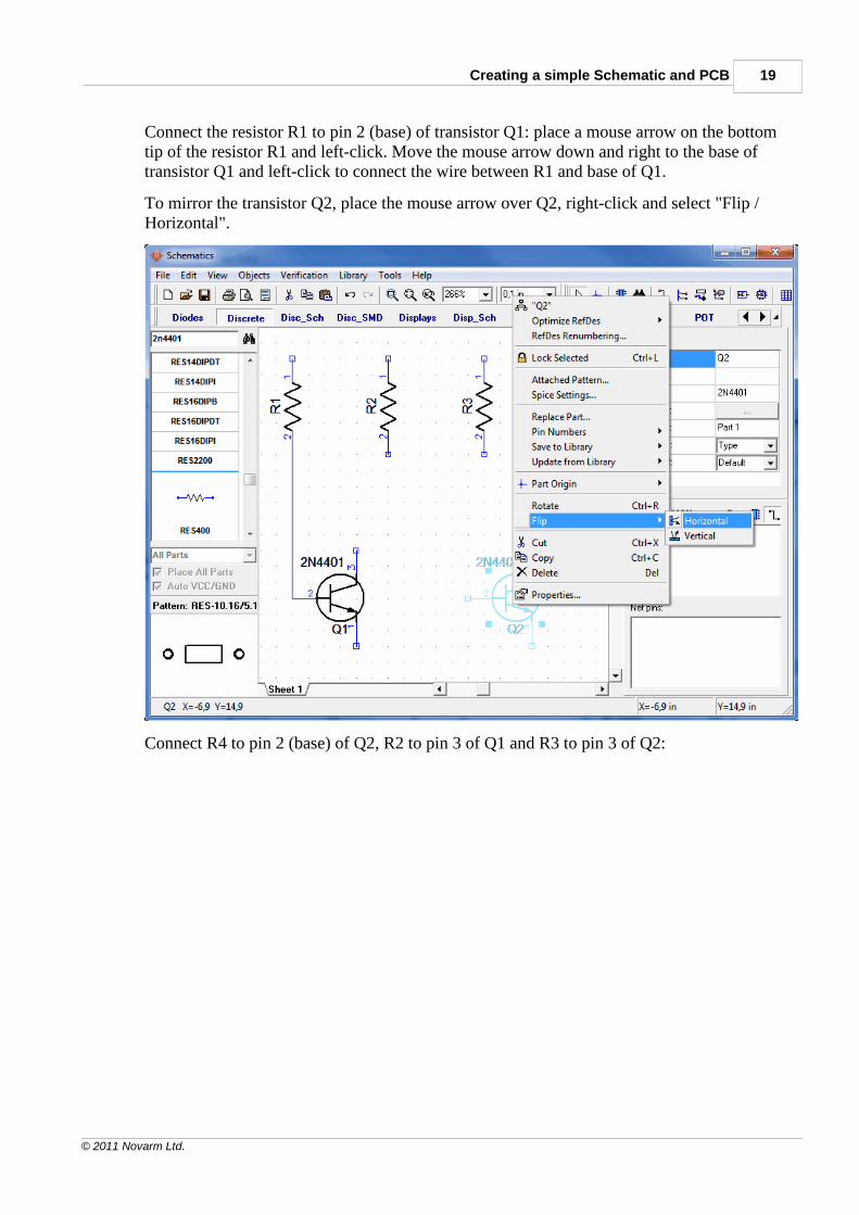
Connect the resistor R1 to pin 2 (base) of transistor Q1: place a mouse arrow on the bottomtip of the resistor R1 and left-click. Move the mouse arrow down and right to the base oftransistor Q1 and left-click to connect the wire between R1 and base of Q1.
To mirror the transistor Q2, place the mouse arrow over Q2, right-click and select "Flip /Horizontal".
Connect R4 to pin 2 (base) of Q2, R2 to pin 3 of Q1 and R3 to pin 3 of Q2:
DipTrace Tutorial20
© 2011 Novarm Ltd.
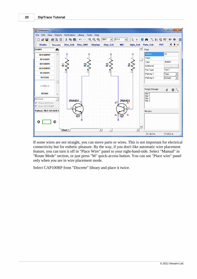
If some wires are not straight, you can move parts or wires. This is not important for electricalconnectivity but for esthetic pleasure. By the way, if you don't like automatic wire placementfeature, you can turn it off in "Place Wire" panel to your right-hand-side. Select "Manual" in"Route Mode" section, or just press "M" quick-access button. You can see "Place wire" panelonly when you are in wire placement mode.
Select CAP100RP from "Discrete" library and place it twice.
Creating a simple Schematic and PCB 21
© 2011 Novarm Ltd.
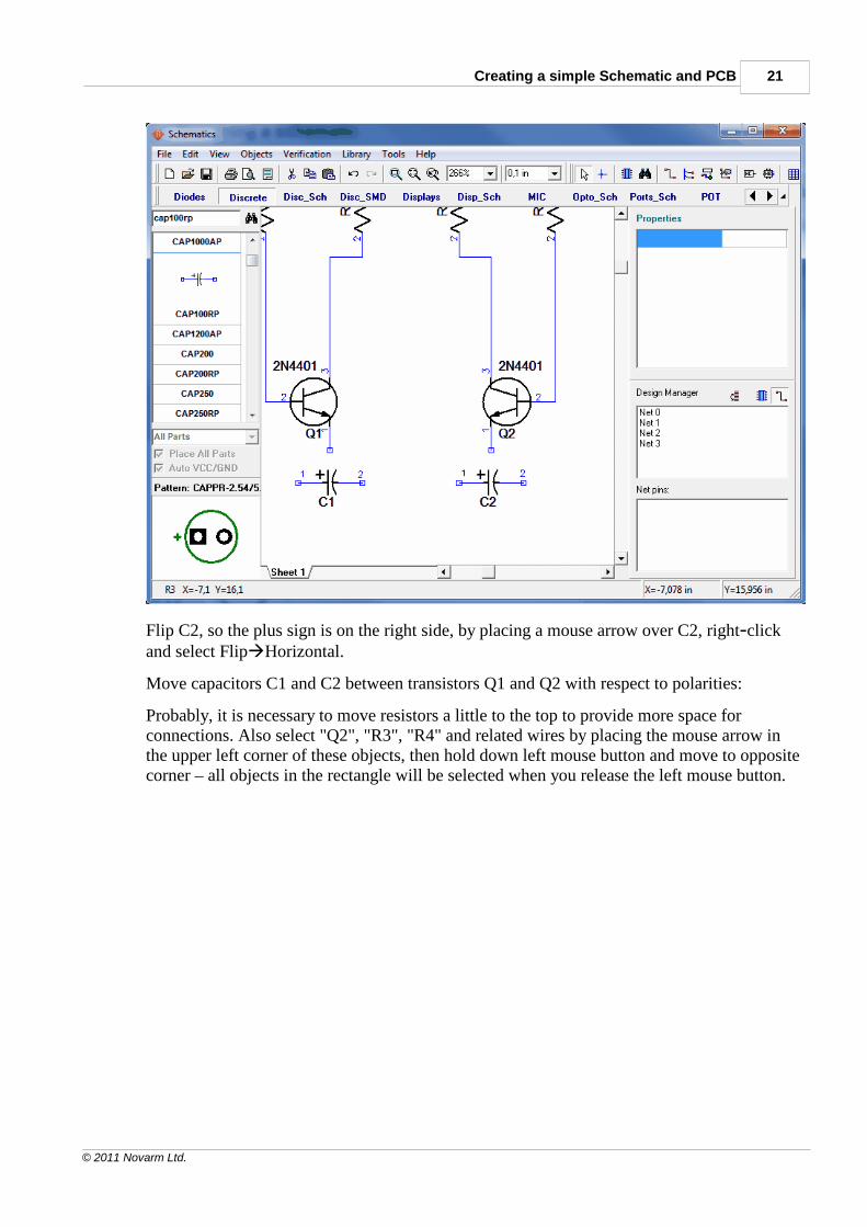
Flip C2, so the plus sign is on the right side, by placing a mouse arrow over C2, right-clickand select Flip Horizontal.
Move capacitors C1 and C2 between transistors Q1 and Q2 with respect to polarities:
Probably, it is necessary to move resistors a little to the top to provide more space forconnections. Also select "Q2", "R3", "R4" and related wires by placing the mouse arrow inthe upper left corner of these objects, then hold down left mouse button and move to oppositecorner – all objects in the rectangle will be selected when you release the left mouse button.
DipTrace Tutorial22
© 2011 Novarm Ltd.
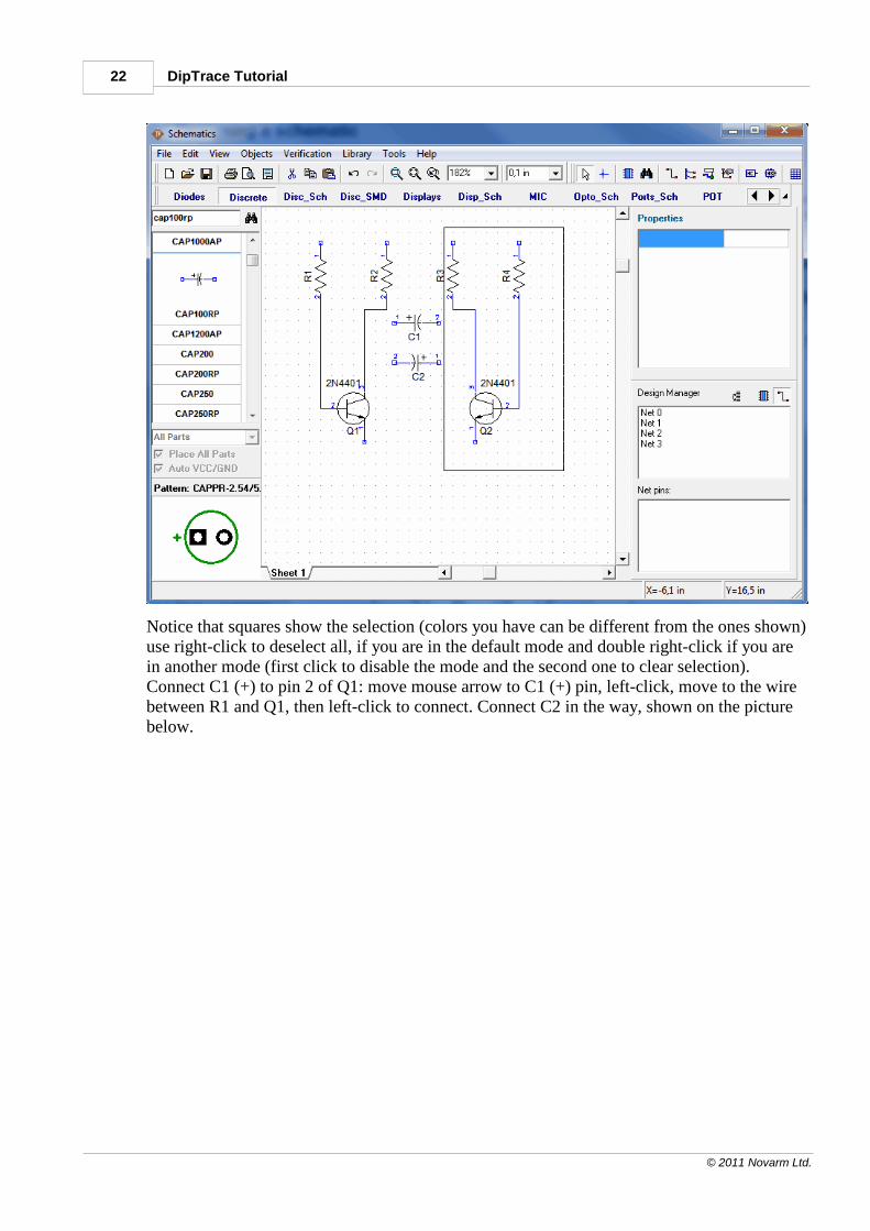
Notice that squares show the selection (colors you have can be different from the ones shown)use right-click to deselect all, if you are in the default mode and double right-click if you arein another mode (first click to disable the mode and the second one to clear selection).Connect C1 (+) to pin 2 of Q1: move mouse arrow to C1 (+) pin, left-click, move to the wirebetween R1 and Q1, then left-click to connect. Connect C2 in the way, shown on the picturebelow.
Creating a simple Schematic and PCB 23
© 2011 Novarm Ltd.
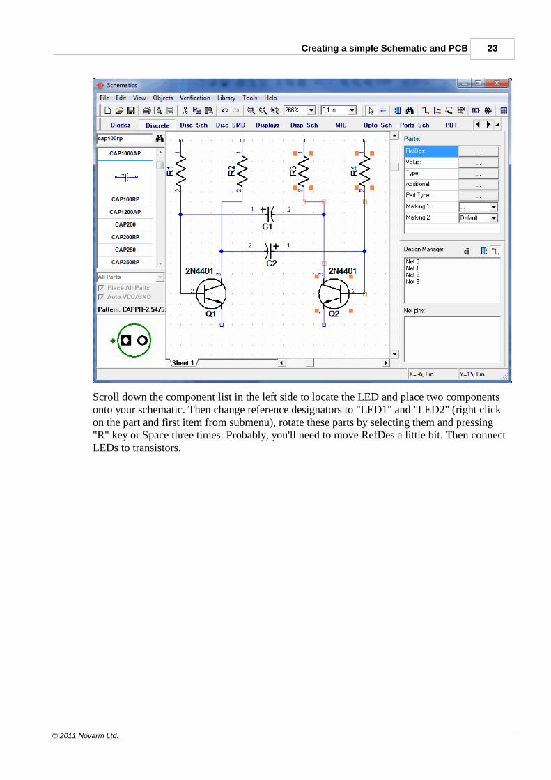
Scroll down the component list in the left side to locate the LED and place two componentsonto your schematic. Then change reference designators to "LED1" and "LED2" (right clickon the part and first item from submenu), rotate these parts by selecting them and pressing"R" key or Space three times. Probably, you'll need to move RefDes a little bit. Then connectLEDs to transistors.
DipTrace Tutorial24
© 2011 Novarm Ltd.
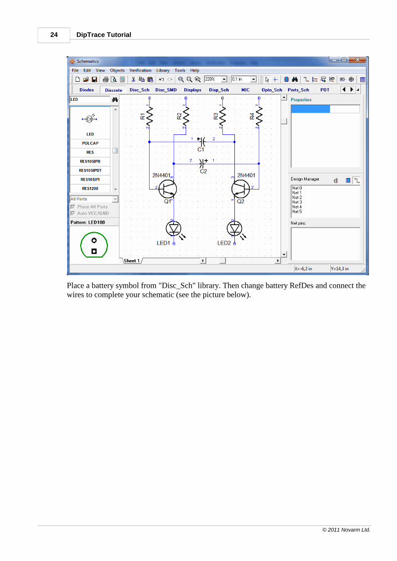
Place a battery symbol from "Disc_Sch" library. Then change battery RefDes and connect thewires to complete your schematic (see the picture below).
Creating a simple Schematic and PCB 25
© 2011 Novarm Ltd.
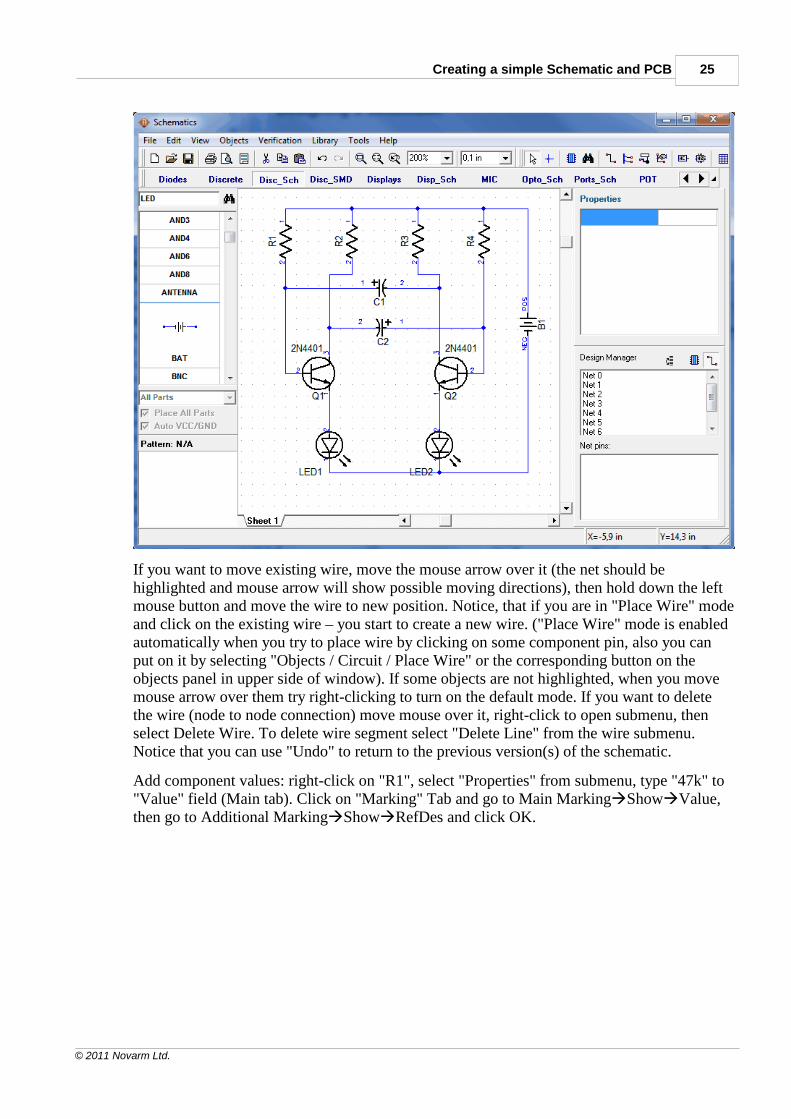
If you want to move existing wire, move the mouse arrow over it (the net should behighlighted and mouse arrow will show possible moving directions), then hold down the leftmouse button and move the wire to new position. Notice, that if you are in "Place Wire" modeand click on the existing wire – you start to create a new wire. ("Place Wire" mode is enabledautomatically when you try to place wire by clicking on some component pin, also you canput on it by selecting "Objects / Circuit / Place Wire" or the corresponding button on theobjects panel in upper side of window). If some objects are not highlighted, when you movemouse arrow over them try right-clicking to turn on the default mode. If you want to deletethe wire (node to node connection) move mouse over it, right-click to open submenu, thenselect Delete Wire. To delete wire segment select "Delete Line" from the wire submenu.Notice that you can use "Undo" to return to the previous version(s) of the schematic.
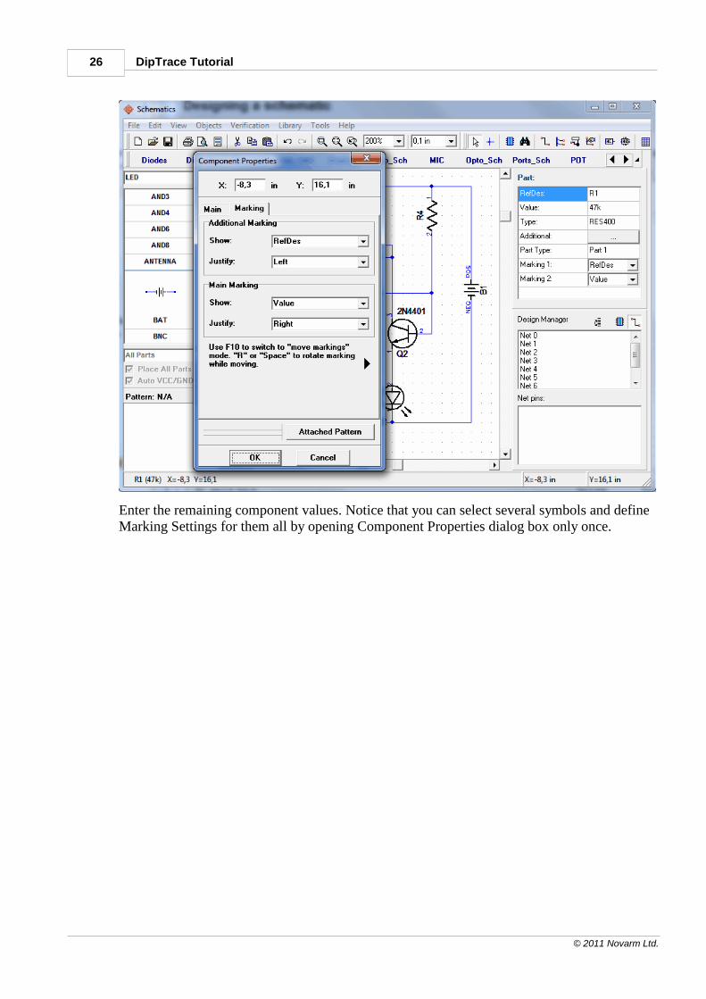
Add component values: right-click on "R1", select "Properties" from submenu, type "47k" to"Value" field (Main tab). Click on "Marking" Tab and go to Main Marking Show Value,then go to Additional Marking Show RefDes and click OK.
DipTrace Tutorial26
© 2011 Novarm Ltd.
Enter the remaining component values. Notice that you can select several symbols and defineMarking Settings for them all by opening Component Properties dialog box only once.
Creating a simple Schematic and PCB 27
© 2011 Novarm Ltd.
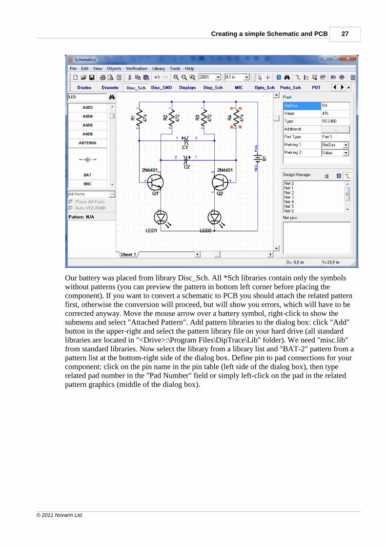
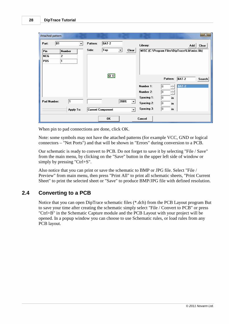
Our battery was placed from library Disc_Sch. All *Sch libraries contain only the symbolswithout patterns (you can preview the pattern in bottom left corner before placing thecomponent). If you want to convert a schematic to PCB you should attach the related patternfirst, otherwise the conversion will proceed, but will show you errors, which will have to becorrected anyway. Move the mouse arrow over a battery symbol, right-click to show thesubmenu and select "Attached Pattern". Add pattern libraries to the dialog box: click "Add"button in the upper-right and select the pattern library file on your hard drive (all standardlibraries are located in "<Drive>:\Program Files\DipTrace\Lib" folder). We need "misc.lib"from standard libraries. Now select the library from a library list and "BAT-2" pattern from apattern list at the bottom-right side of the dialog box. Define pin to pad connections for yourcomponent: click on the pin name in the pin table (left side of the dialog box), then typerelated pad number in the "Pad Number" field or simply left-click on the pad in the relatedpattern graphics (middle of the dialog box).
DipTrace Tutorial28
© 2011 Novarm Ltd.
When pin to pad connections are done, click OK.
Note: some symbols may not have the attached patterns (for example VCC, GND or logicalconnectors – "Net Ports") and that will be shown in "Errors" during conversion to a PCB.
Our schematic is ready to convert to PCB. Do not forget to save it by selecting "File / Save"from the main menu, by clicking on the "Save" button in the upper left side of window orsimply by pressing "Ctrl+S".
Also notice that you can print or save the schematic to BMP or JPG file. Select "File /Preview" from main menu, then press "Print All" to print all schematic sheets, "Print CurrentSheet" to print the selected sheet or "Save" to produce BMP/JPG file with defined resolution.
2.4 Converting to a PCB
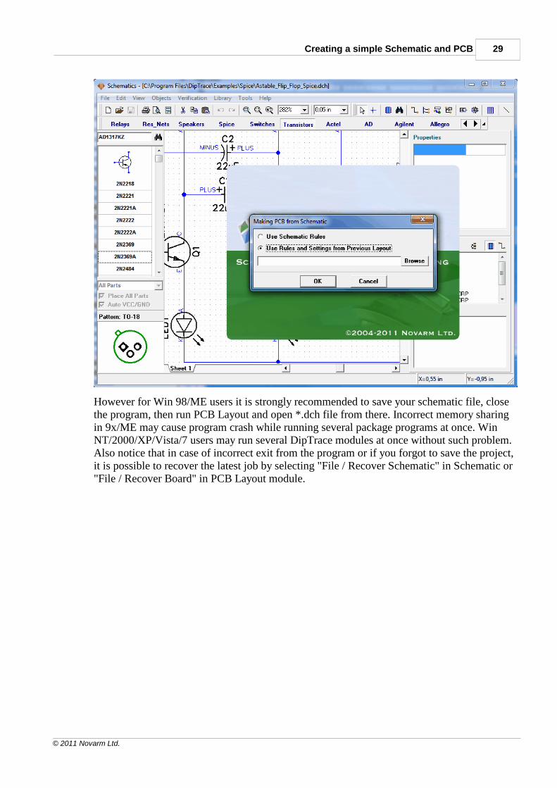
Notice that you can open DipTrace schematic files (*.dch) from the PCB Layout program Butto save your time after creating the schematic simply select "File / Convert to PCB" or press"Ctrl+B" in the Schematic Capture module and the PCB Layout with your project will beopened. In a popup window you can choose to use Schematic rules, or load rules from anyPCB layout.
Creating a simple Schematic and PCB 29
© 2011 Novarm Ltd.
However for Win 98/ME users it is strongly recommended to save your schematic file, closethe program, then run PCB Layout and open *.dch file from there. Incorrect memory sharingin 9x/ME may cause program crash while running several package programs at once. WinNT/2000/XP/Vista/7 users may run several DipTrace modules at once without such problem.Also notice that in case of incorrect exit from the program or if you forgot to save the project,it is possible to recover the latest job by selecting "File / Recover Schematic" in Schematic or"File / Recover Board" in PCB Layout module.
DipTrace Tutorial30
© 2011 Novarm Ltd.
If you plan to use another PCB Layout software to design a PCB or give it to someone else,you can use netlist export feature of Schematic program. Select "File / Export / Netlist" frommain menu, then netlist format. DipTrace supports popular netlist formats, such as Tango,PADS, P-CAD, etc. Also this feature is useful to check net structure.
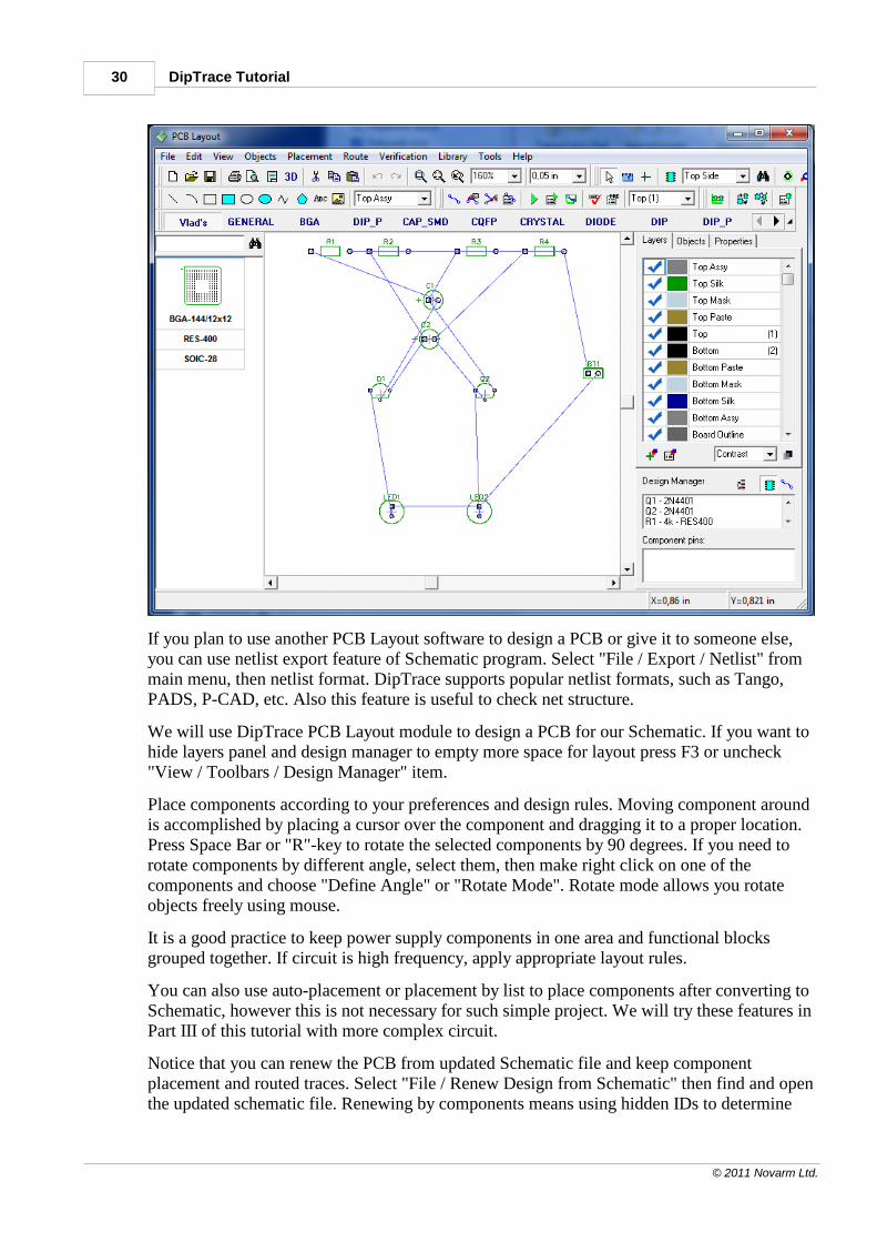
We will use DipTrace PCB Layout module to design a PCB for our Schematic. If you want tohide layers panel and design manager to empty more space for layout press F3 or uncheck"View / Toolbars / Design Manager" item.
Place components according to your preferences and design rules. Moving component aroundis accomplished by placing a cursor over the component and dragging it to a proper location.Press Space Bar or "R"-key to rotate the selected components by 90 degrees. If you need torotate components by different angle, select them, then make right click on one of thecomponents and choose "Define Angle" or "Rotate Mode". Rotate mode allows you rotateobjects freely using mouse.
It is a good practice to keep power supply components in one area and functional blocksgrouped together. If circuit is high frequency, apply appropriate layout rules.
You can also use auto-placement or placement by list to place components after converting toSchematic, however this is not necessary for such simple project. We will try these features inPart III of this tutorial with more complex circuit.
Notice that you can renew the PCB from updated Schematic file and keep componentplacement and routed traces. Select "File / Renew Design from Schematic" then find and openthe updated schematic file. Renewing by components means using hidden IDs to determine
Creating a simple Schematic and PCB 31
© 2011 Novarm Ltd.
component/pattern links - this will work only if PCB was made directly from Schematic,RefDes may be different. Renewing by RefDes means that component/pattern links aredetermined by RefDes - in this case PCB can be designed separately, but RefDes should besimilar. Upating from Related Schematic means updating by components from the relatedschematic file (see File/Design Information).
2.5 Designing a PCB
2.5.1 Preparing to route
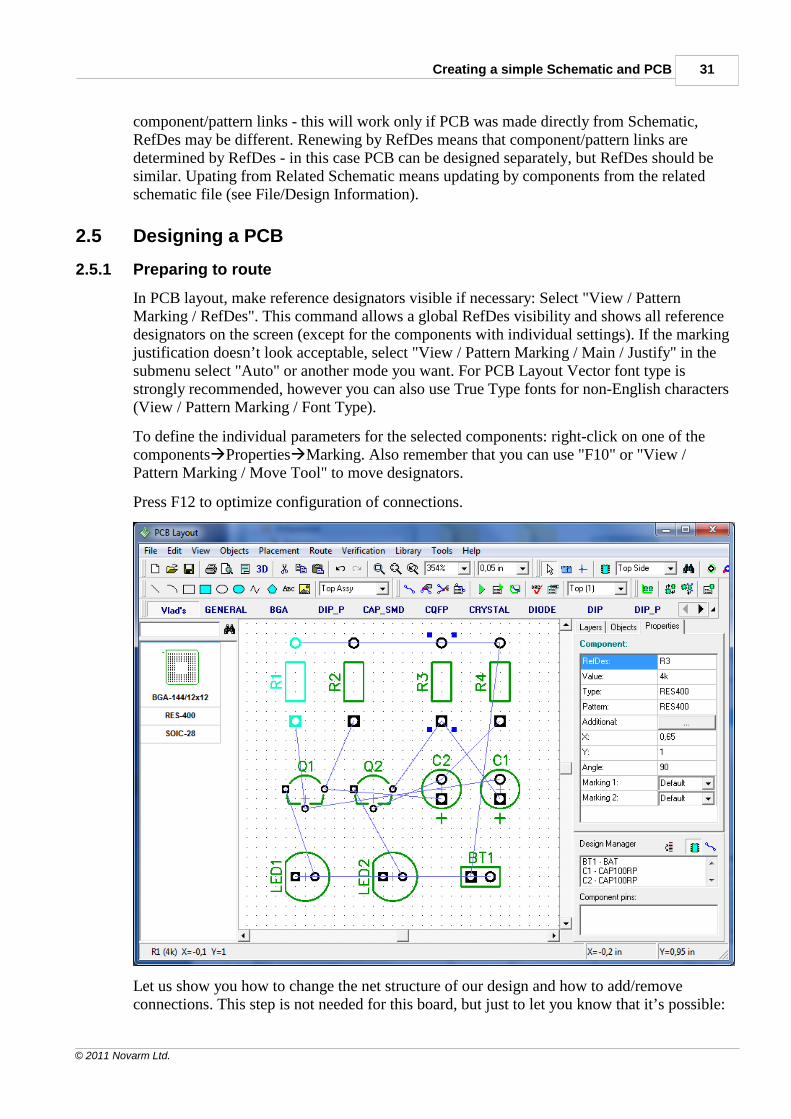
In PCB layout, make reference designators visible if necessary: Select "View / PatternMarking / RefDes". This command allows a global RefDes visibility and shows all referencedesignators on the screen (except for the components with individual settings). If the markingjustification doesn’t look acceptable, select "View / Pattern Marking / Main / Justify" in thesubmenu select "Auto" or another mode you want. For PCB Layout Vector font type isstrongly recommended, however you can also use True Type fonts for non-English characters(View / Pattern Marking / Font Type).
To define the individual parameters for the selected components: right-click on one of thecomponents Properties Marking. Also remember that you can use "F10" or "View /Pattern Marking / Move Tool" to move designators.
Press F12 to optimize configuration of connections.
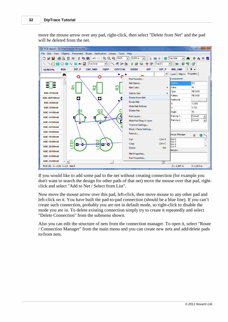
Let us show you how to change the net structure of our design and how to add/removeconnections. This step is not needed for this board, but just to let you know that it’s possible:
DipTrace Tutorial32
© 2011 Novarm Ltd.
move the mouse arrow over any pad, right-click, then select "Delete from Net" and the padwill be deleted from the net.
If you would like to add some pad to the net without creating connection (for example youdon't want to search the design for other pads of that net) move the mouse over that pad, right-click and select "Add to Net / Select from List".
Now move the mouse arrow over this pad, left-click, then move mouse to any other pad andleft-click on it. You have built the pad-to-pad connection (should be a blue line). If you can’tcreate such connection, probably you are not in default mode, so right-click to disable themode you are in. To delete existing connection simply try to create it repeatedly and select"Delete Connection" from the submenu shown.
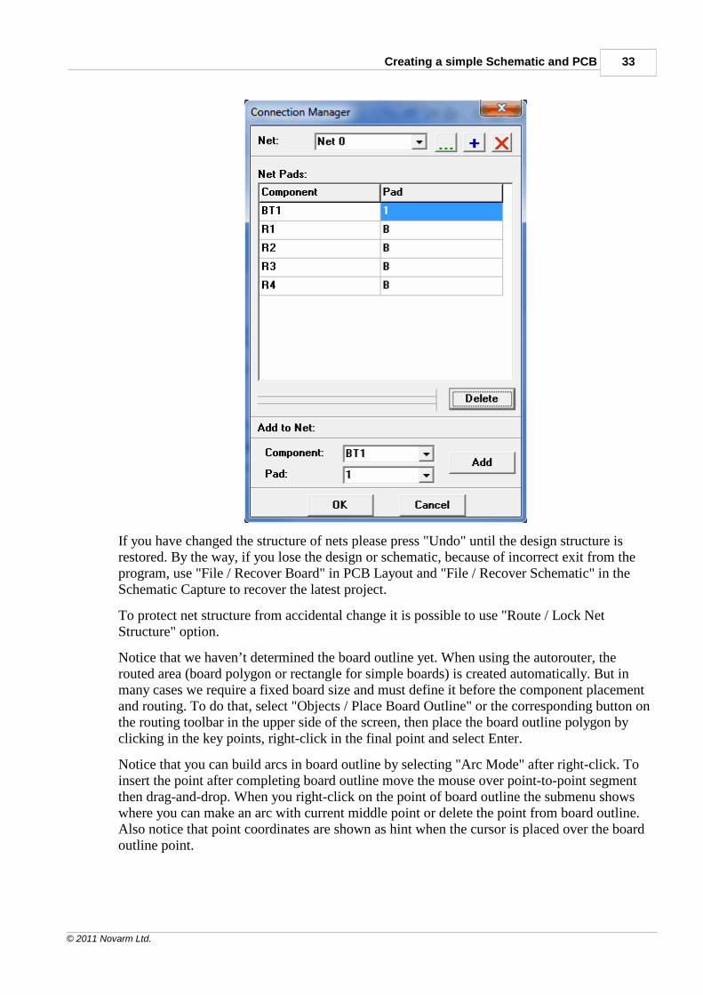
Also you can edit the structure of nets from the connection manager. To open it, select "Route/ Connection Manager" from the main menu and you can create new nets and add/delete padsto/from nets.
Creating a simple Schematic and PCB 33
© 2011 Novarm Ltd.
If you have changed the structure of nets please press "Undo" until the design structure isrestored. By the way, if you lose the design or schematic, because of incorrect exit from theprogram, use "File / Recover Board" in PCB Layout and "File / Recover Schematic" in theSchematic Capture to recover the latest project.
To protect net structure from accidental change it is possible to use "Route / Lock NetStructure" option.
Notice that we haven’t determined the board outline yet. When using the autorouter, therouted area (board polygon or rectangle for simple boards) is created automatically. But inmany cases we require a fixed board size and must define it before the component placementand routing. To do that, select "Objects / Place Board Outline" or the corresponding button onthe routing toolbar in the upper side of the screen, then place the board outline polygon byclicking in the key points, right-click in the final point and select Enter.
Notice that you can build arcs in board outline by selecting "Arc Mode" after right-click. Toinsert the point after completing board outline move the mouse over point-to-point segmentthen drag-and-drop. When you right-click on the point of board outline the submenu showswhere you can make an arc with current middle point or delete the point from board outline.Also notice that point coordinates are shown as hint when the cursor is placed over the boardoutline point.
DipTrace Tutorial34
© 2011 Novarm Ltd.
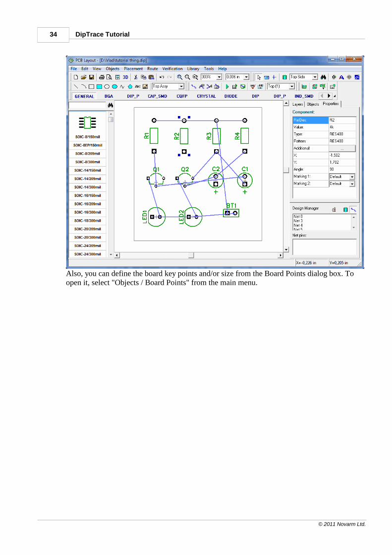
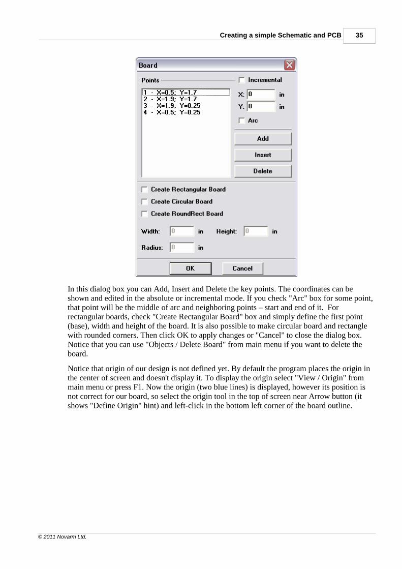
Also, you can define the board key points and/or size from the Board Points dialog box. Toopen it, select "Objects / Board Points" from the main menu.
Creating a simple Schematic and PCB 35
© 2011 Novarm Ltd.
In this dialog box you can Add, Insert and Delete the key points. The coordinates can beshown and edited in the absolute or incremental mode. If you check "Arc" box for some point,that point will be the middle of arc and neighboring points – start and end of it. Forrectangular boards, check "Create Rectangular Board" box and simply define the first point(base), width and height of the board. It is also possible to make circular board and rectanglewith rounded corners. Then click OK to apply changes or "Cancel" to close the dialog box.Notice that you can use "Objects / Delete Board" from main menu if you want to delete theboard.
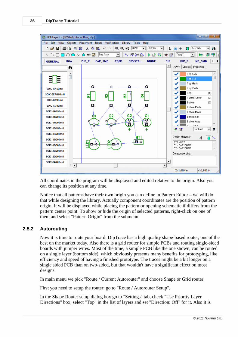
Notice that origin of our design is not defined yet. By default the program places the origin inthe center of screen and doesn't display it. To display the origin select "View / Origin" frommain menu or press F1. Now the origin (two blue lines) is displayed, however its position isnot correct for our board, so select the origin tool in the top of screen near Arrow button (itshows "Define Origin" hint) and left-click in the bottom left corner of the board outline.
DipTrace Tutorial36
© 2011 Novarm Ltd.
All coordinates in the program will be displayed and edited relative to the origin. Also youcan change its position at any time.
Notice that all patterns have their own origin you can define in Pattern Editor – we will dothat while designing the library. Actually component coordinates are the position of patternorigin. It will be displayed while placing the pattern or opening schematic if differs from thepattern center point. To show or hide the origin of selected patterns, right-click on one ofthem and select "Pattern Origin" from the submenu.
2.5.2 Autorouting
Now it is time to route your board. DipTrace has a high quality shape-based router, one of thebest on the market today. Also there is a grid router for simple PCBs and routing single-sidedboards with jumper wires. Most of the time, a simple PCB like the one shown, can be routedon a single layer (bottom side), which obviously presents many benefits for prototyping, likeefficiency and speed of having a finished prototype. The traces might be a bit longer on asingle sided PCB than on two-sided, but that wouldn't have a significant effect on mostdesigns.
In main menu we pick "Route / Current Autorouter" and choose Shape or Grid router.
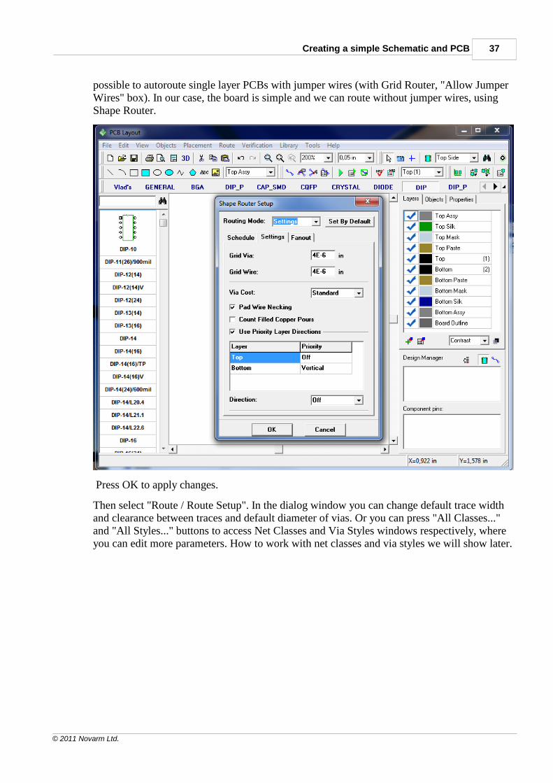
First you need to setup the router: go to "Route / Autorouter Setup".
In the Shape Router setup dialog box go to "Settings" tab, check "Use Priority LayerDirections" box, select "Top" in the list of layers and set "Direction: Off" for it. Also it is
Creating a simple Schematic and PCB 37
© 2011 Novarm Ltd.
possible to autoroute single layer PCBs with jumper wires (with Grid Router, "Allow JumperWires" box). In our case, the board is simple and we can route without jumper wires, usingShape Router.
Press OK to apply changes.
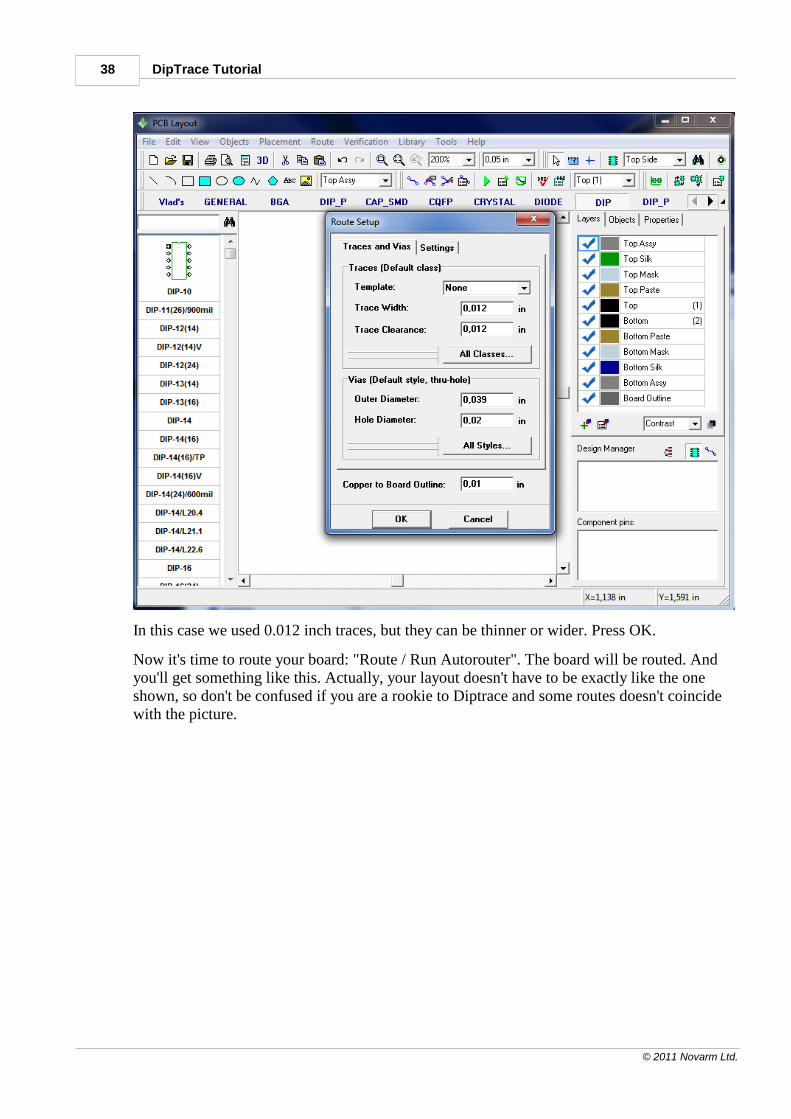
Then select "Route / Route Setup". In the dialog window you can change default trace widthand clearance between traces and default diameter of vias. Or you can press "All Classes..."and "All Styles..." buttons to access Net Classes and Via Styles windows respectively, whereyou can edit more parameters. How to work with net classes and via styles we will show later.
DipTrace Tutorial38
© 2011 Novarm Ltd.
In this case we used 0.012 inch traces, but they can be thinner or wider. Press OK.
Now it's time to route your board: "Route / Run Autorouter". The board will be routed. Andyou'll get something like this. Actually, your layout doesn't have to be exactly like the oneshown, so don't be confused if you are a rookie to Diptrace and some routes doesn't coincidewith the picture.
Creating a simple Schematic and PCB 39
© 2011 Novarm Ltd.
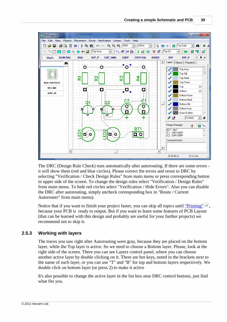
The DRC (Design Rule Check) runs automatically after autorouting. If there are some errors -it will show them (red and blue circles). Please correct the errors and rerun to DRC byselecting "Verification / Check Design Rules" from main menu or press corresponding buttonin upper side of the screen. To change the design rules select "Verification / Design Rules"from main menu. To hide red circles select "Verification / Hide Errors". Also you can disablethe DRC after autorouting, simply uncheck corresponding box in "Route / CurrentAutorouter" from main menu).
Notice that if you want to finish your project faster, you can skip all topics until "Printing" ,because your PCB is ready to output. But if you want to learn some features of PCB Layout(that can be learned with this design and probably are useful for your further projects) werecommend not to skip it.
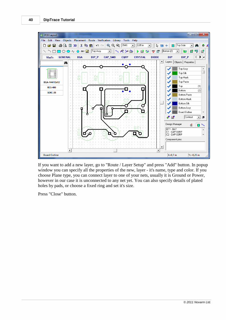
2.5.3 Working with layers
The traces you saw right after Autorouting were gray, because they are placed on the bottomlayer, while the Top layer is active. So we need to choose a Bottom layer. Please, look at theright side of the screen. There you can see Layers control panel, where you can chooseanother active layer by double clicking on it. There are hot keys, noted in the brackets next tothe name of each layer, or you can use "T" and "B" for top and bottom layers respectively. Wedouble click on bottom layer (or press 2) to make it active
It's also possible to change the active layer in the list box near DRC control buttons, just findwhat fits you.
77
DipTrace Tutorial40
© 2011 Novarm Ltd.
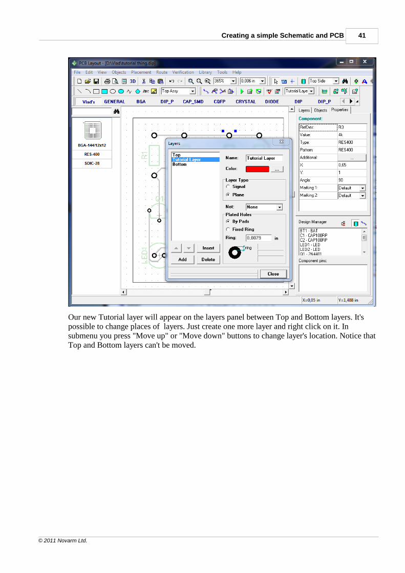
If you want to add a new layer, go to "Route / Layer Setup" and press "Add" button. In popupwindow you can specify all the properties of the new, layer - it's name, type and color. If youchoose Plane type, you can connect layer to one of your nets, usually it is Ground or Power,however in our case it is unconnected to any net yet. You can also specify details of platedholes by pads, or choose a fixed ring and set it's size.
Press "Close" button.
Creating a simple Schematic and PCB 41
© 2011 Novarm Ltd.
Our new Tutorial layer will appear on the layers panel between Top and Bottom layers. It'spossible to change places of layers. Just create one more layer and right click on it. Insubmenu you press "Move up" or "Move down" buttons to change layer's location. Notice thatTop and Bottom layers can't be moved.
DipTrace Tutorial42
© 2011 Novarm Ltd.
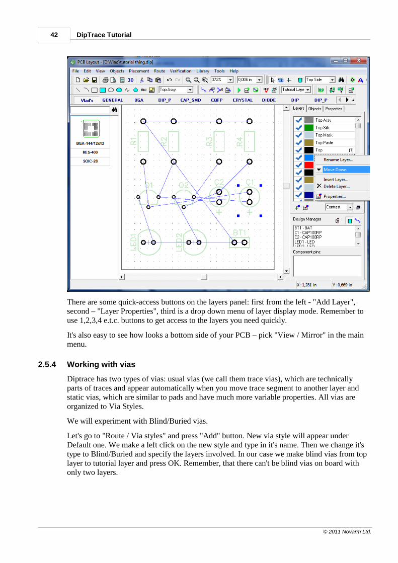
There are some quick-access buttons on the layers panel: first from the left - "Add Layer",second – "Layer Properties", third is a drop down menu of layer display mode. Remember touse 1,2,3,4 e.t.c. buttons to get access to the layers you need quickly.
It's also easy to see how looks a bottom side of your PCB – pick "View / Mirror" in the mainmenu.
2.5.4 Working with vias
Diptrace has two types of vias: usual vias (we call them trace vias), which are technicallyparts of traces and appear automatically when you move trace segment to another layer andstatic vias, which are similar to pads and have much more variable properties. All vias areorganized to Via Styles.
We will experiment with Blind/Buried vias.
Let's go to "Route / Via styles" and press "Add" button. New via style will appear underDefault one. We make a left click on the new style and type in it's name. Then we change it'stype to Blind/Buried and specify the layers involved. In our case we make blind vias from toplayer to tutorial layer and press OK. Remember, that there can't be blind vias on board withonly two layers.
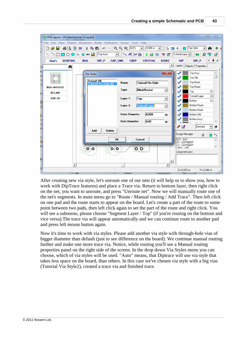
Creating a simple Schematic and PCB 43
© 2011 Novarm Ltd.
After creating new via style, let's unroute one of our nets (it will help us to show you, how towork with DipTrace features) and place a Trace via. Return to bottom layer, then right clickon the net, you want to unroute, and press "Unroute net". Now we will manually route one ofthe net's segments. In main menu go to "Route / Manual routing / Add Trace". Then left clickon one pad and the route starts to appear on the board. Let's create a part of the route to somepoint between two pads, then left click again to set the part of the route and right click. Youwill see a submenu, please choose "Segment Layer / Top" (if you're routing on the bottom andvice versa).The trace via will appear automatically and we can continue route to another padand press left mouse button again.
Now it's time to work with via styles. Please add another via style with through-hole vias ofbigger diameter than default (just to see difference on the board). We continue manual routingfurther and make one more trace via. Notice, while routing you'll see a Manual routingproperties panel on the right side of the screen. In the drop down Via Styles menu you canchoose, which of via styles will be used. "Auto" means, that Diptrace will use via style thattakes less space on the board, than others. In this case we've chosen via style with a big vias(Tutorial Via Style2), created a trace via and finished trace.
DipTrace Tutorial44
© 2011 Novarm Ltd.
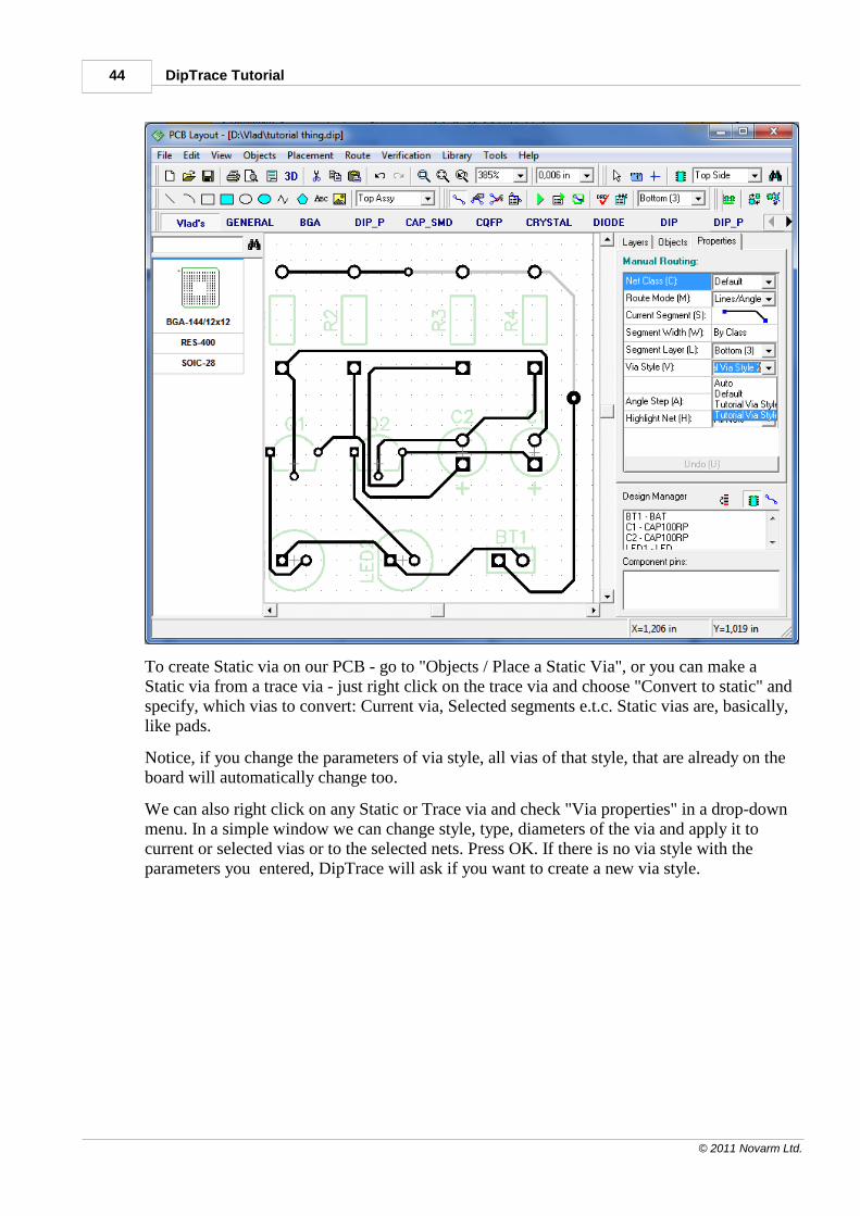
To create Static via on our PCB - go to "Objects / Place a Static Via", or you can make aStatic via from a trace via - just right click on the trace via and choose "Convert to static" andspecify, which vias to convert: Current via, Selected segments e.t.c. Static vias are, basically,like pads.
Notice, if you change the parameters of via style, all vias of that style, that are already on theboard will automatically change too.
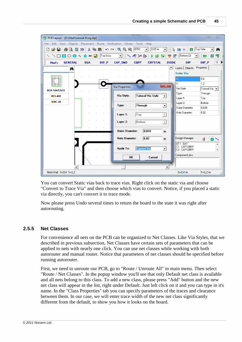
We can also right click on any Static or Trace via and check "Via properties" in a drop-downmenu. In a simple window we can change style, type, diameters of the via and apply it tocurrent or selected vias or to the selected nets. Press OK. If there is no via style with theparameters you entered, DipTrace will ask if you want to create a new via style.
Creating a simple Schematic and PCB 45
© 2011 Novarm Ltd.
You can convert Static vias back to trace vias. Right click on the static via and choose"Convert to Trace Via" and then choose which vias to convert. Notice, if you placed a staticvia directly, you can't convert it to trace mode.
Now please press Undo several times to return the board to the state it was right afterautorouting.
2.5.5 Net Classes
For convenience all nets on the PCB can be organized to Net Classes. Like Via Styles, that wedescribed in previous subsection, Net Classes have certain sets of parameters that can beapplied to nets with nearly one click. You can use net classes while working with bothautorouter and manual router. Notice that parameters of net classes should be specified beforerunning autorouter.
First, we need to unroute our PCB, go to "Route / Unroute All" in main menu. Then select"Route / Net Classes". In the popup window you'll see that only Default net class is availableand all nets belong to this class. To add a new class, please press "Add" button and the newnet class will appear in the list, right under Default. Just left click on it and you can type in it'sname. In the "Class Properties" tab you can specify parameters of the traces and clearancebetween them. In our case, we will enter trace width of the new net class significantlydifferent from the default, to show you how it looks on the board.
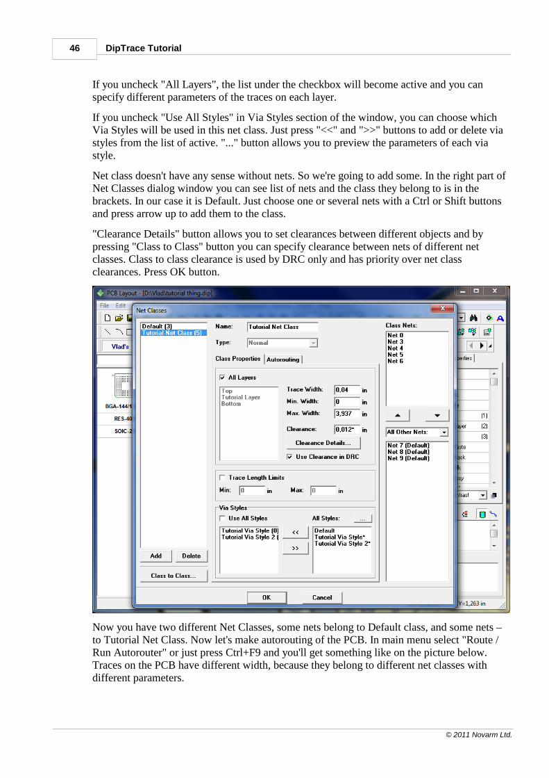
DipTrace Tutorial46
© 2011 Novarm Ltd.
If you uncheck "All Layers", the list under the checkbox will become active and you canspecify different parameters of the traces on each layer.
If you uncheck "Use All Styles" in Via Styles section of the window, you can choose whichVia Styles will be used in this net class. Just press "<<" and ">>" buttons to add or delete viastyles from the list of active. "..." button allows you to preview the parameters of each viastyle.
Net class doesn't have any sense without nets. So we're going to add some. In the right part ofNet Classes dialog window you can see list of nets and the class they belong to is in thebrackets. In our case it is Default. Just choose one or several nets with a Ctrl or Shift buttonsand press arrow up to add them to the class.
"Clearance Details" button allows you to set clearances between different objects and bypressing "Class to Class" button you can specify clearance between nets of different netclasses. Class to class clearance is used by DRC only and has priority over net classclearances. Press OK button.
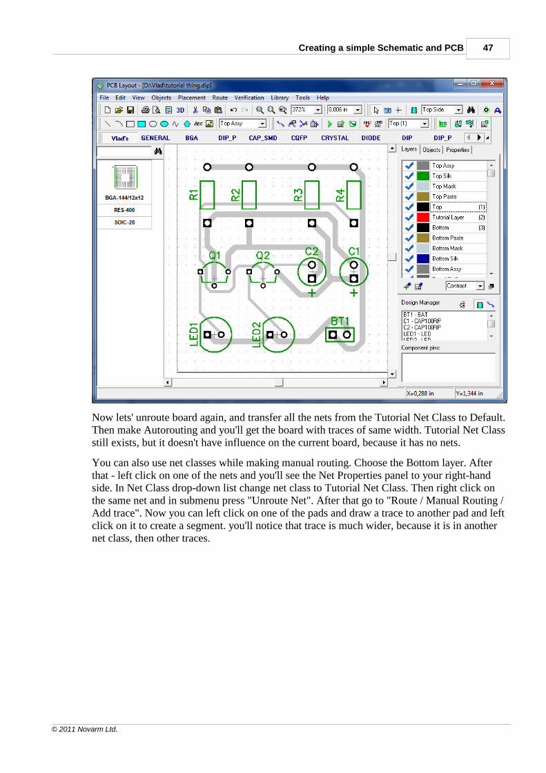
Now you have two different Net Classes, some nets belong to Default class, and some nets –to Tutorial Net Class. Now let's make autorouting of the PCB. In main menu select "Route /Run Autorouter" or just press Ctrl+F9 and you'll get something like on the picture below.Traces on the PCB have different width, because they belong to different net classes withdifferent parameters.
Creating a simple Schematic and PCB 47
© 2011 Novarm Ltd.
Now lets' unroute board again, and transfer all the nets from the Tutorial Net Class to Default.Then make Autorouting and you'll get the board with traces of same width. Tutorial Net Classstill exists, but it doesn't have influence on the current board, because it has no nets.
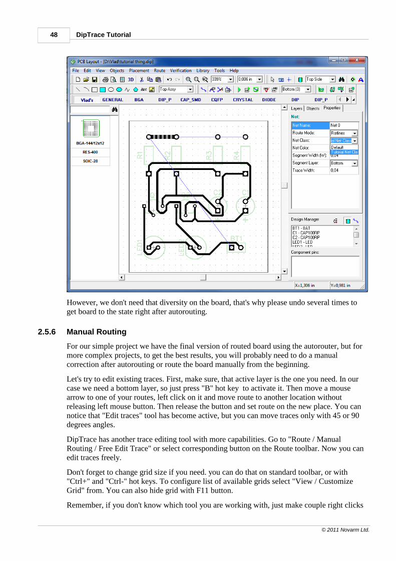
You can also use net classes while making manual routing. Choose the Bottom layer. Afterthat - left click on one of the nets and you'll see the Net Properties panel to your right-handside. In Net Class drop-down list change net class to Tutorial Net Class. Then right click onthe same net and in submenu press "Unroute Net". After that go to "Route / Manual Routing /Add trace". Now you can left click on one of the pads and draw a trace to another pad and leftclick on it to create a segment. you'll notice that trace is much wider, because it is in anothernet class, then other traces.
DipTrace Tutorial48
© 2011 Novarm Ltd.
However, we don't need that diversity on the board, that's why please undo several times toget board to the state right after autorouting.
2.5.6 Manual Routing
For our simple project we have the final version of routed board using the autorouter, but formore complex projects, to get the best results, you will probably need to do a manualcorrection after autorouting or route the board manually from the beginning.
Let's try to edit existing traces. First, make sure, that active layer is the one you need. In ourcase we need a bottom layer, so just press "B" hot key to activate it. Then move a mousearrow to one of your routes, left click on it and move route to another location withoutreleasing left mouse button. Then release the button and set route on the new place. You cannotice that "Edit traces" tool has become active, but you can move traces only with 45 or 90degrees angles.
DipTrace has another trace editing tool with more capabilities. Go to "Route / ManualRouting / Free Edit Trace" or select corresponding button on the Route toolbar. Now you canedit traces freely.
Don't forget to change grid size if you need. you can do that on standard toolbar, or with"Ctrl+" and "Ctrl-" hot keys. To configure list of available grids select "View / CustomizeGrid" from. You can also hide grid with F11 button.
Remember, if you don't know which tool you are working with, just make couple right clicks
Creating a simple Schematic and PCB 49
© 2011 Novarm Ltd.
on free part of the board and DipTrace will return to default.
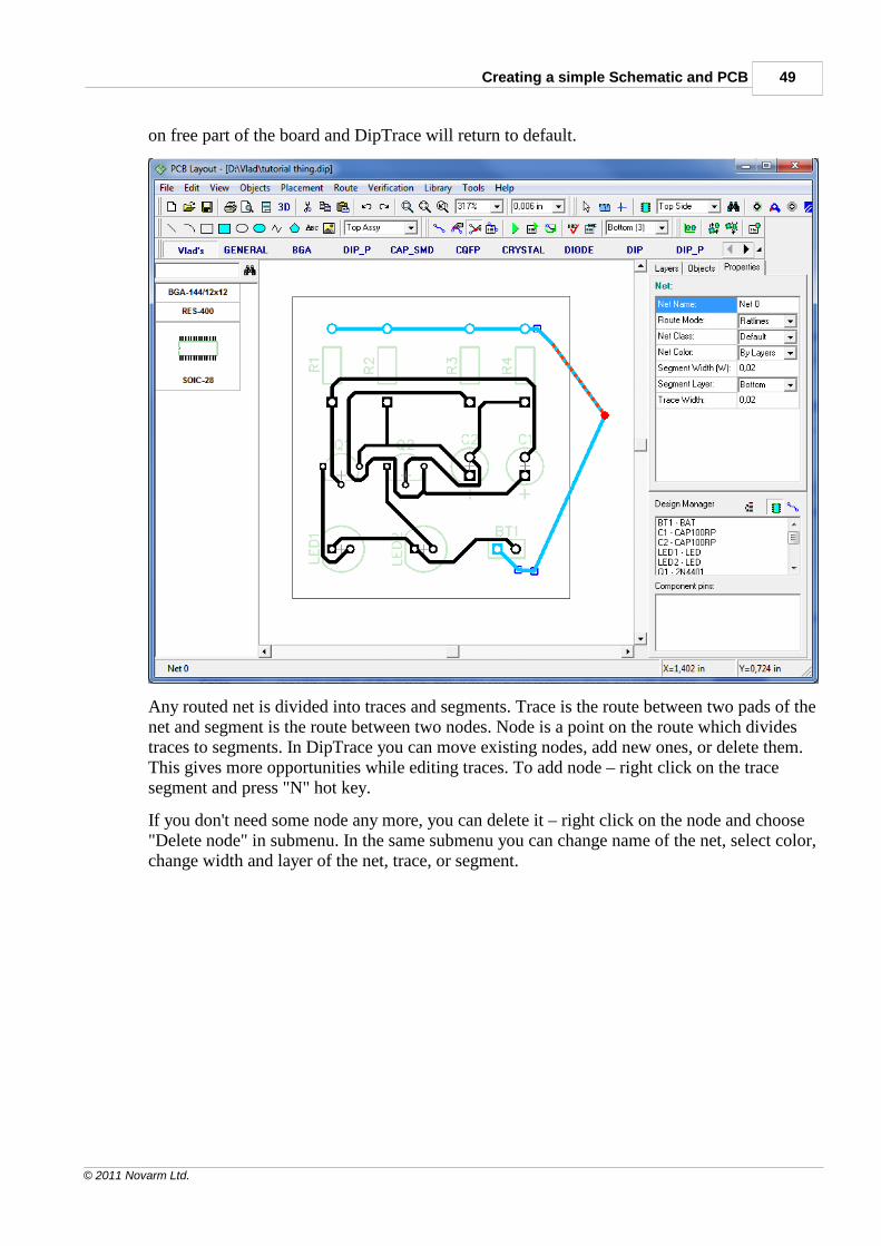
Any routed net is divided into traces and segments. Trace is the route between two pads of thenet and segment is the route between two nodes. Node is a point on the route which dividestraces to segments. In DipTrace you can move existing nodes, add new ones, or delete them.This gives more opportunities while editing traces. To add node – right click on the tracesegment and press "N" hot key.
If you don't need some node any more, you can delete it – right click on the node and choose"Delete node" in submenu. In the same submenu you can change name of the net, select color,change width and layer of the net, trace, or segment.
DipTrace Tutorial50
© 2011 Novarm Ltd.
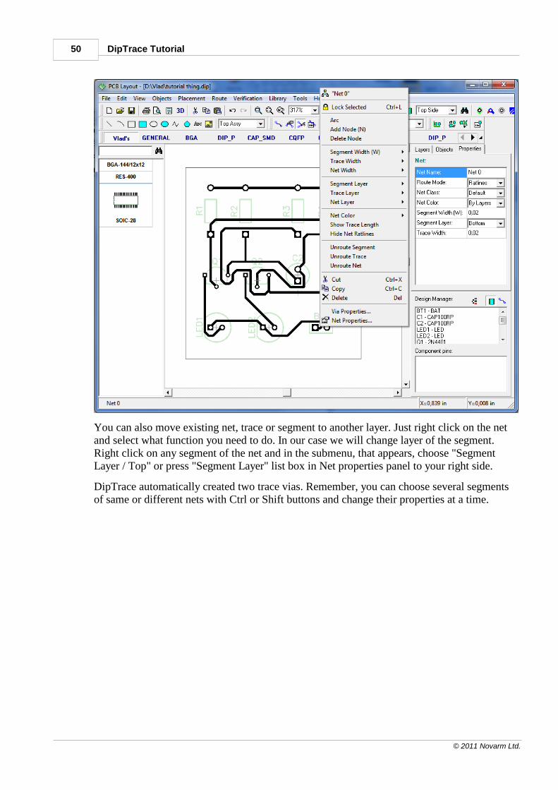
You can also move existing net, trace or segment to another layer. Just right click on the netand select what function you need to do. In our case we will change layer of the segment.Right click on any segment of the net and in the submenu, that appears, choose "SegmentLayer / Top" or press "Segment Layer" list box in Net properties panel to your right side.
DipTrace automatically created two trace vias. Remember, you can choose several segmentsof same or different nets with Ctrl or Shift buttons and change their properties at a time.
Creating a simple Schematic and PCB 51
© 2011 Novarm Ltd.
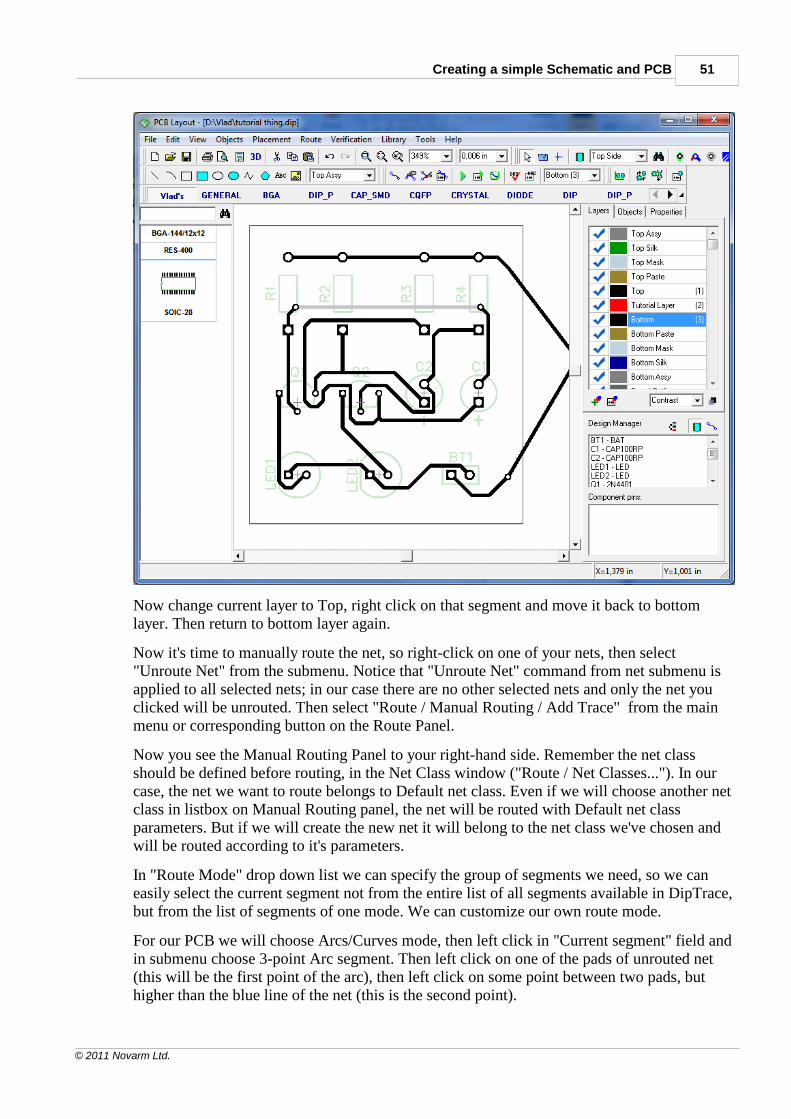
Now change current layer to Top, right click on that segment and move it back to bottomlayer. Then return to bottom layer again.
Now it's time to manually route the net, so right-click on one of your nets, then select"Unroute Net" from the submenu. Notice that "Unroute Net" command from net submenu isapplied to all selected nets; in our case there are no other selected nets and only the net youclicked will be unrouted. Then select "Route / Manual Routing / Add Trace" from the mainmenu or corresponding button on the Route Panel.
Now you see the Manual Routing Panel to your right-hand side. Remember the net classshould be defined before routing, in the Net Class window ("Route / Net Classes..."). In ourcase, the net we want to route belongs to Default net class. Even if we will choose another netclass in listbox on Manual Routing panel, the net will be routed with Default net classparameters. But if we will create the new net it will belong to the net class we've chosen andwill be routed according to it's parameters.
In "Route Mode" drop down list we can specify the group of segments we need, so we caneasily select the current segment not from the entire list of all segments available in DipTrace,but from the list of segments of one mode. We can customize our own route mode.
For our PCB we will choose Arcs/Curves mode, then left click in "Current segment" field andin submenu choose 3-point Arc segment. Then left click on one of the pads of unrouted net(this will be the first point of the arc), then left click on some point between two pads, buthigher than the blue line of the net (this is the second point).
DipTrace Tutorial52
© 2011 Novarm Ltd.
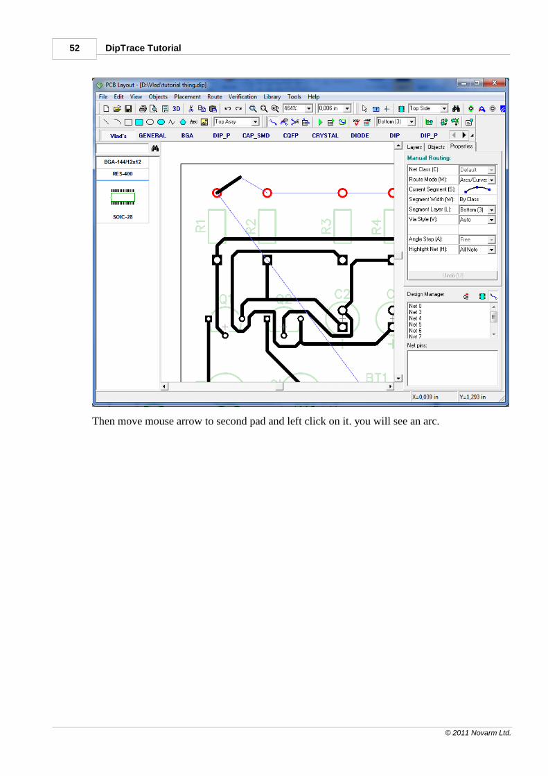
Then move mouse arrow to second pad and left click on it. you will see an arc.
Creating a simple Schematic and PCB 53
© 2011 Novarm Ltd.
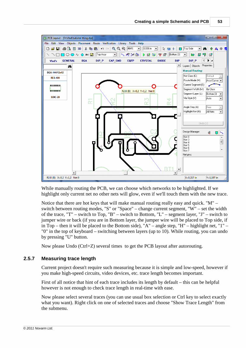
While manually routing the PCB, we can choose which networks to be highlighted. If wehighlight only current net no other nets will glow, even if we'll touch them with the new trace.
Notice that there are hot keys that will make manual routing really easy and quick. "M" –switch between routing modes, "S" or "Space" – change current segment, "W" – set the widthof the trace, "T" – switch to Top, "B" – switch to Bottom, "L" – segment layer, "J" – switch tojumper wire or back (if you are in Bottom layer, the jumper wire will be placed to Top side, ifin Top – then it will be placed to the Bottom side), "A" – angle step, "H" – highlight net, "1" –"0" in the top of keyboard – switching between layers (up to 10). While routing, you can undoby pressing "U" button.
Now please Undo (Ctrl+Z) several times to get the PCB layout after autorouting.
2.5.7 Measuring trace length
Current project doesn't require such measuring because it is simple and low-speed, however ifyou make high-speed circuits, video devices, etc. trace length becomes important.
First of all notice that hint of each trace includes its length by default – this can be helpfulhowever is not enough to check trace length in real-time with ease.
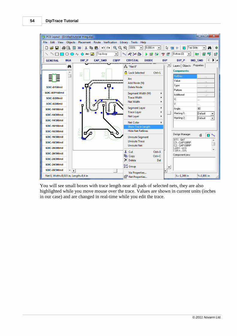
Now please select several traces (you can use usual box selection or Ctrl key to select exactlywhat you want). Right click on one of selected traces and choose "Show Trace Length" fromthe submenu.
DipTrace Tutorial54
© 2011 Novarm Ltd.
You will see small boxes with trace length near all pads of selected nets, they are alsohighlighted while you move mouse over the trace. Values are shown in current units (inchesin our case) and are changed in real-time while you edit the trace.
Creating a simple Schematic and PCB 55
© 2011 Novarm Ltd.
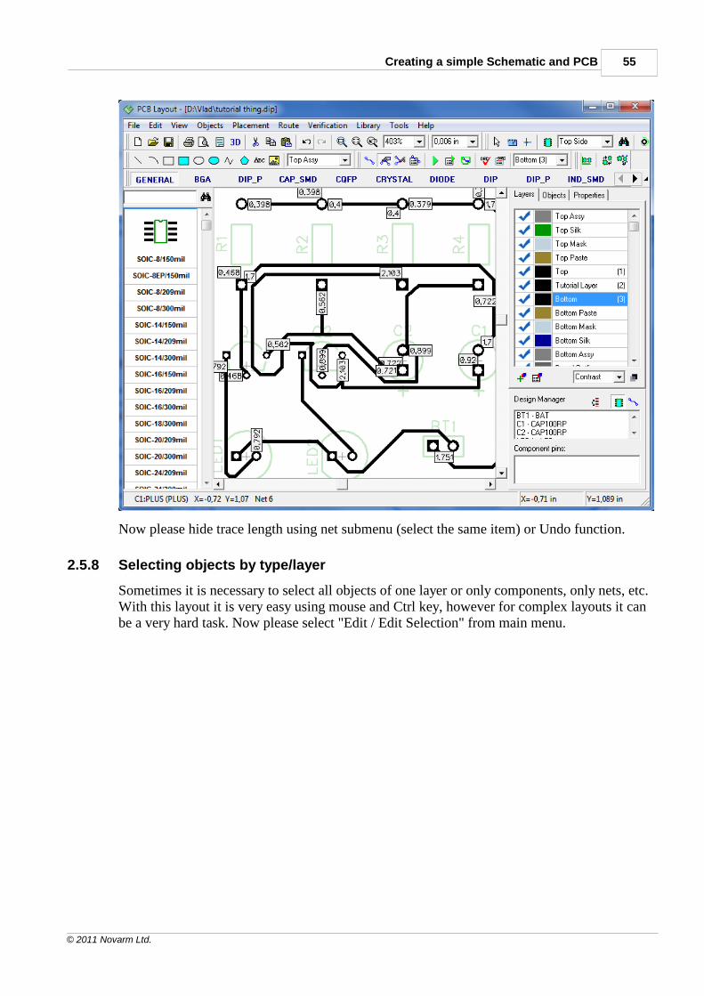
Now please hide trace length using net submenu (select the same item) or Undo function.
2.5.8 Selecting objects by type/layer
Sometimes it is necessary to select all objects of one layer or only components, only nets, etc.With this layout it is very easy using mouse and Ctrl key, however for complex layouts it canbe a very hard task. Now please select "Edit / Edit Selection" from main menu.
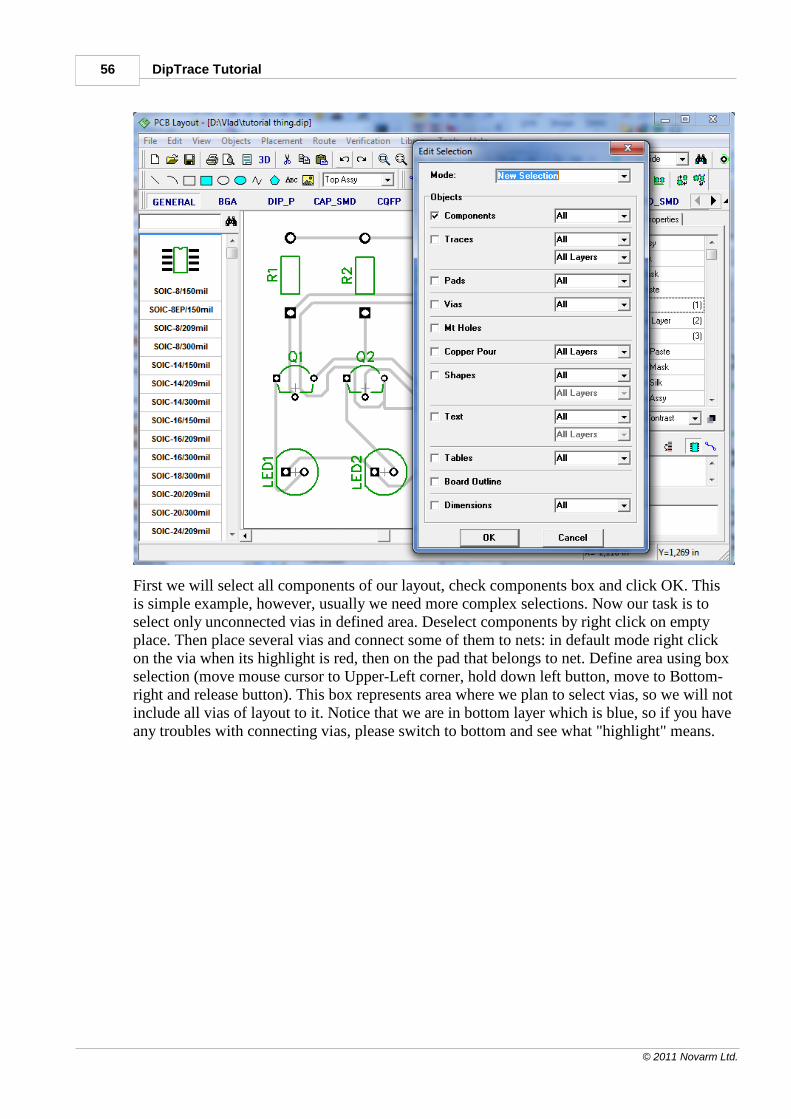
DipTrace Tutorial56
© 2011 Novarm Ltd.
First we will select all components of our layout, check components box and click OK. Thisis simple example, however, usually we need more complex selections. Now our task is toselect only unconnected vias in defined area. Deselect components by right click on emptyplace. Then place several vias and connect some of them to nets: in default mode right clickon the via when its highlight is red, then on the pad that belongs to net. Define area using boxselection (move mouse cursor to Upper-Left corner, hold down left button, move to Bottom-right and release button). This box represents area where we plan to select vias, so we will notinclude all vias of layout to it. Notice that we are in bottom layer which is blue, so if you haveany troubles with connecting vias, please switch to bottom and see what "highlight" means.
Creating a simple Schematic and PCB 57
© 2011 Novarm Ltd.
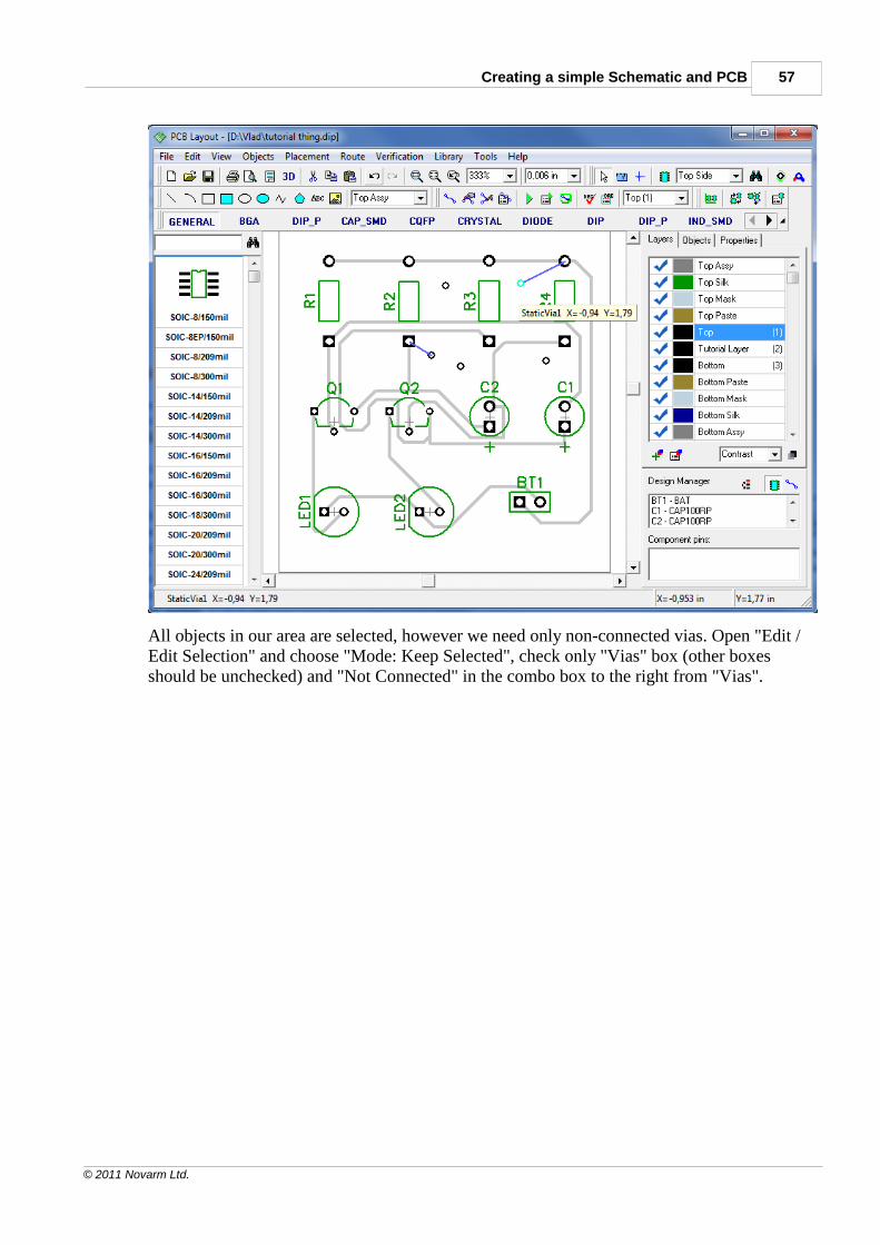
All objects in our area are selected, however we need only non-connected vias. Open "Edit /Edit Selection" and choose "Mode: Keep Selected", check only "Vias" box (other boxesshould be unchecked) and "Not Connected" in the combo box to the right from "Vias".
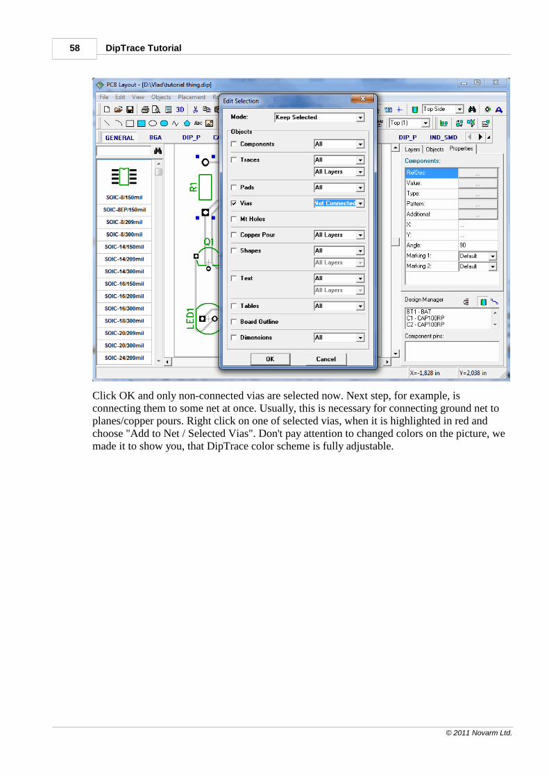
DipTrace Tutorial58
© 2011 Novarm Ltd.
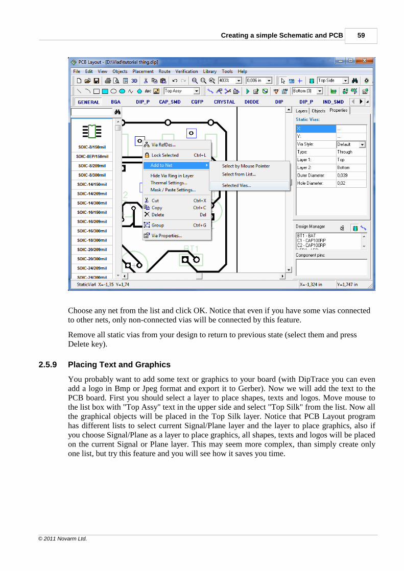
Click OK and only non-connected vias are selected now. Next step, for example, isconnecting them to some net at once. Usually, this is necessary for connecting ground net toplanes/copper pours. Right click on one of selected vias, when it is highlighted in red andchoose "Add to Net / Selected Vias". Don't pay attention to changed colors on the picture, wemade it to show you, that DipTrace color scheme is fully adjustable.
Creating a simple Schematic and PCB 59
© 2011 Novarm Ltd.
Choose any net from the list and click OK. Notice that even if you have some vias connectedto other nets, only non-connected vias will be connected by this feature.
Remove all static vias from your design to return to previous state (select them and pressDelete key).
2.5.9 Placing Text and Graphics
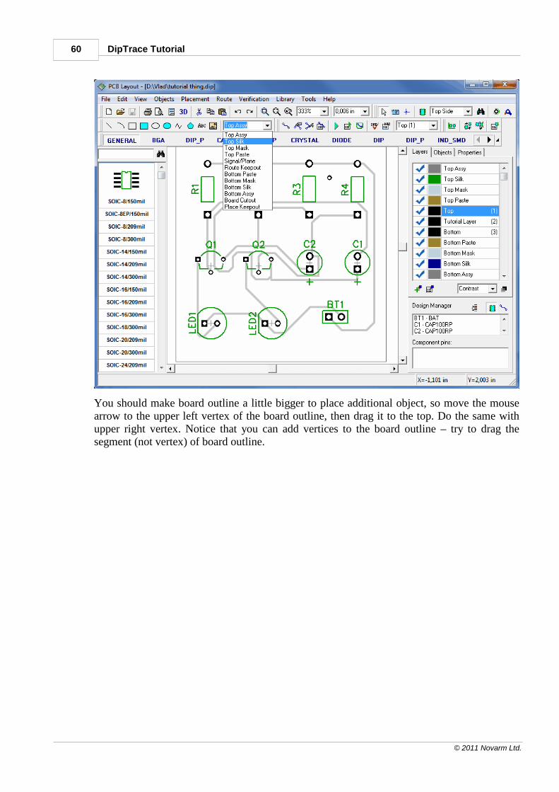
You probably want to add some text or graphics to your board (with DipTrace you can evenadd a logo in Bmp or Jpeg format and export it to Gerber). Now we will add the text to thePCB board. First you should select a layer to place shapes, texts and logos. Move mouse tothe list box with "Top Assy" text in the upper side and select "Top Silk" from the list. Now allthe graphical objects will be placed in the Top Silk layer. Notice that PCB Layout programhas different lists to select current Signal/Plane layer and the layer to place graphics, also ifyou choose Signal/Plane as a layer to place graphics, all shapes, texts and logos will be placedon the current Signal or Plane layer. This may seem more complex, than simply create onlyone list, but try this feature and you will see how it saves you time.
DipTrace Tutorial60
© 2011 Novarm Ltd.
You should make board outline a little bigger to place additional object, so move the mousearrow to the upper left vertex of the board outline, then drag it to the top. Do the same withupper right vertex. Notice that you can add vertices to the board outline – try to drag thesegment (not vertex) of board outline.
Creating a simple Schematic and PCB 61
© 2011 Novarm Ltd.
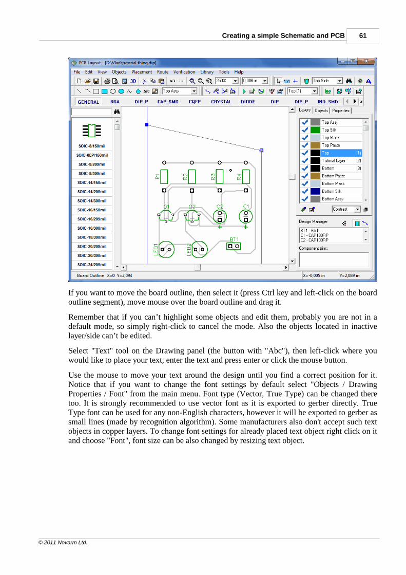
If you want to move the board outline, then select it (press Ctrl key and left-click on the boardoutline segment), move mouse over the board outline and drag it.
Remember that if you can’t highlight some objects and edit them, probably you are not in adefault mode, so simply right-click to cancel the mode. Also the objects located in inactivelayer/side can’t be edited.
Select "Text" tool on the Drawing panel (the button with "Abc"), then left-click where youwould like to place your text, enter the text and press enter or click the mouse button.
Use the mouse to move your text around the design until you find a correct position for it.Notice that if you want to change the font settings by default select "Objects / DrawingProperties / Font" from the main menu. Font type (Vector, True Type) can be changed theretoo. It is strongly recommended to use vector font as it is exported to gerber directly. TrueType font can be used for any non-English characters, however it will be exported to gerber assmall lines (made by recognition algorithm). Some manufacturers also don't accept such textobjects in copper layers. To change font settings for already placed text object right click on itand choose "Font", font size can be also changed by resizing text object.
DipTrace Tutorial62
© 2011 Novarm Ltd.
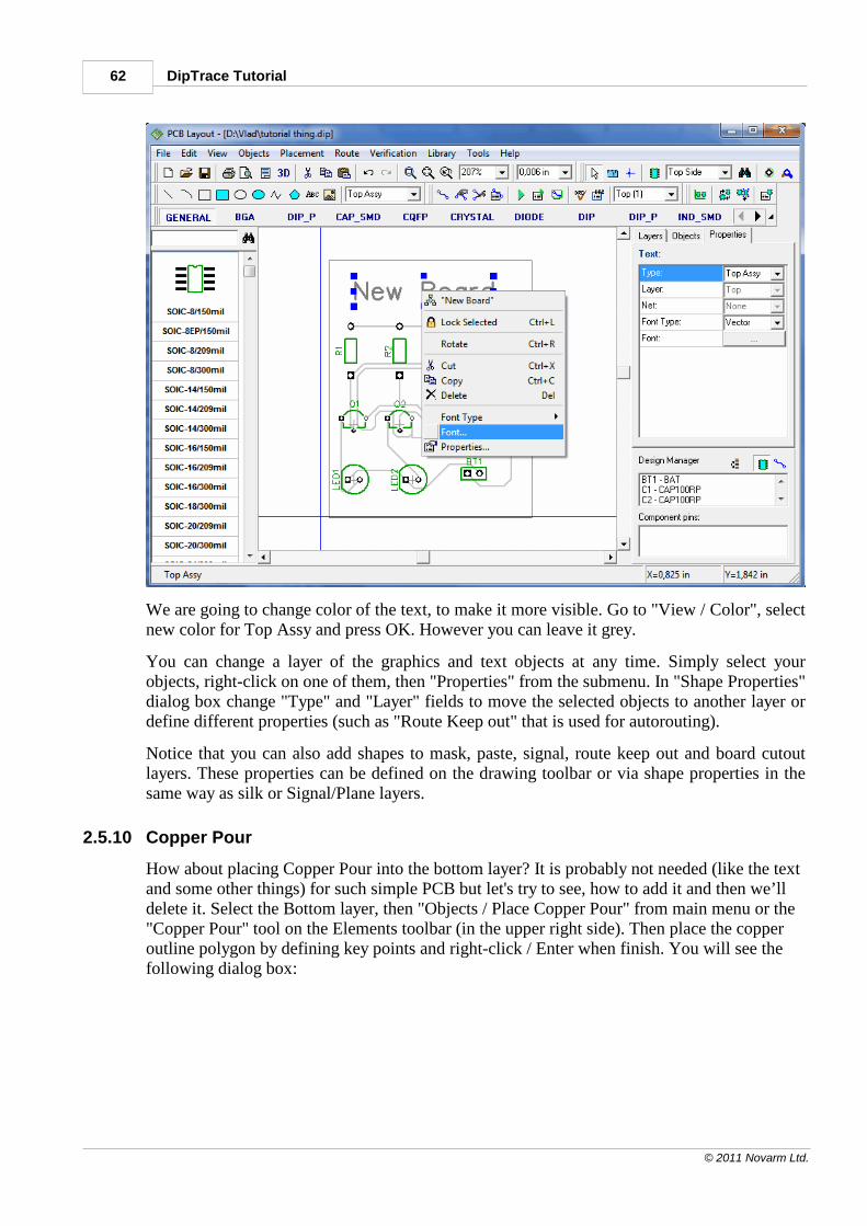
We are going to change color of the text, to make it more visible. Go to "View / Color", selectnew color for Top Assy and press OK. However you can leave it grey.
You can change a layer of the graphics and text objects at any time. Simply select yourobjects, right-click on one of them, then "Properties" from the submenu. In "Shape Properties"dialog box change "Type" and "Layer" fields to move the selected objects to another layer ordefine different properties (such as "Route Keep out" that is used for autorouting).
Notice that you can also add shapes to mask, paste, signal, route keep out and board cutoutlayers. These properties can be defined on the drawing toolbar or via shape properties in thesame way as silk or Signal/Plane layers.
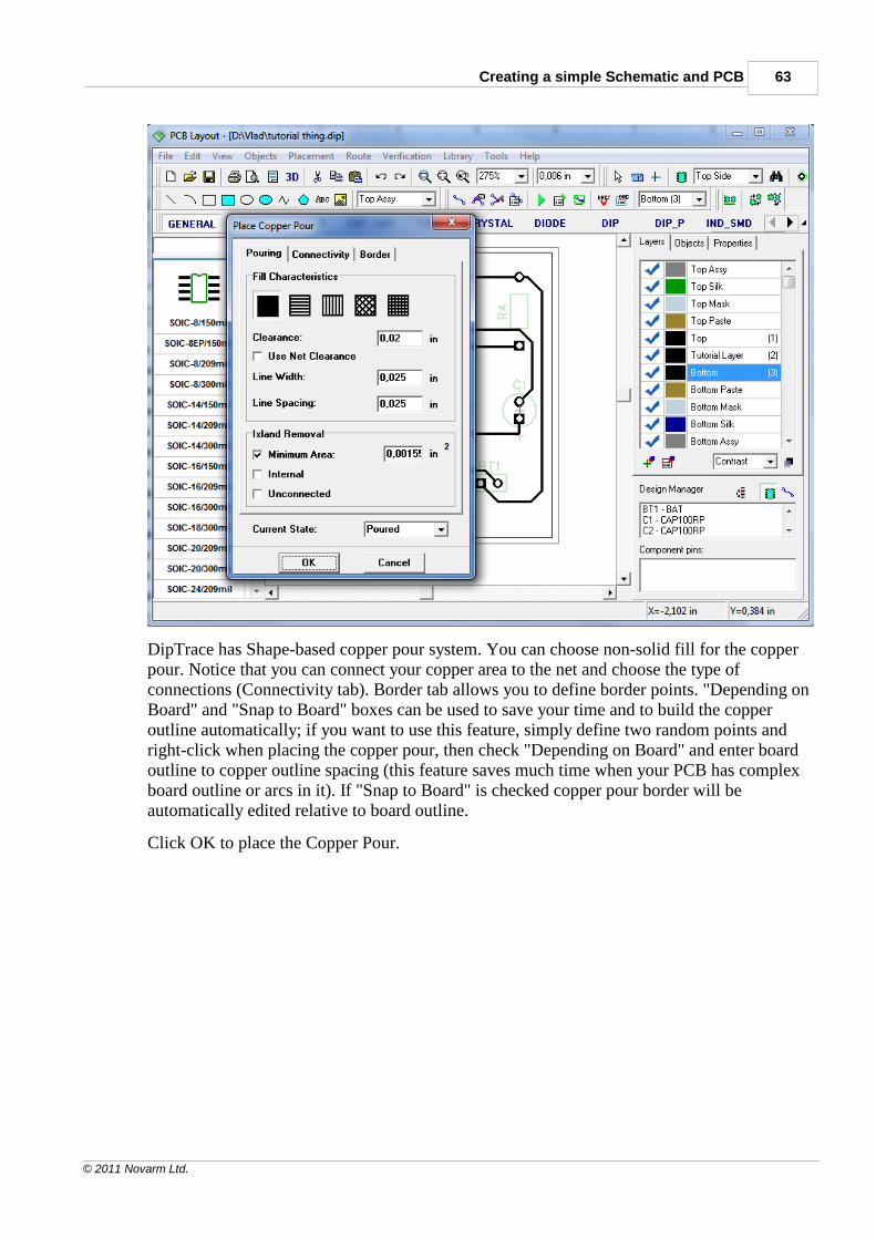
2.5.10 Copper Pour
How about placing Copper Pour into the bottom layer? It is probably not needed (like the textand some other things) for such simple PCB but let's try to see, how to add it and then we’lldelete it. Select the Bottom layer, then "Objects / Place Copper Pour" from main menu or the"Copper Pour" tool on the Elements toolbar (in the upper right side). Then place the copperoutline polygon by defining key points and right-click / Enter when finish. You will see thefollowing dialog box:
Creating a simple Schematic and PCB 63
© 2011 Novarm Ltd.
DipTrace has Shape-based copper pour system. You can choose non-solid fill for the copperpour. Notice that you can connect your copper area to the net and choose the type ofconnections (Connectivity tab). Border tab allows you to define border points. "Depending onBoard" and "Snap to Board" boxes can be used to save your time and to build the copperoutline automatically; if you want to use this feature, simply define two random points andright-click when placing the copper pour, then check "Depending on Board" and enter boardoutline to copper outline spacing (this feature saves much time when your PCB has complexboard outline or arcs in it). If "Snap to Board" is checked copper pour border will beautomatically edited relative to board outline.
Click OK to place the Copper Pour.
DipTrace Tutorial64
© 2011 Novarm Ltd.
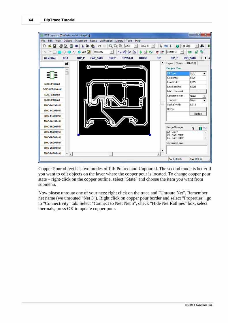
Copper Pour object has two modes of fill: Poured and Unpoured. The second mode is better ifyou want to edit objects on the layer where the copper pour is located. To change copper pourstate – right-click on the copper outline, select "State" and choose the item you want fromsubmenu.
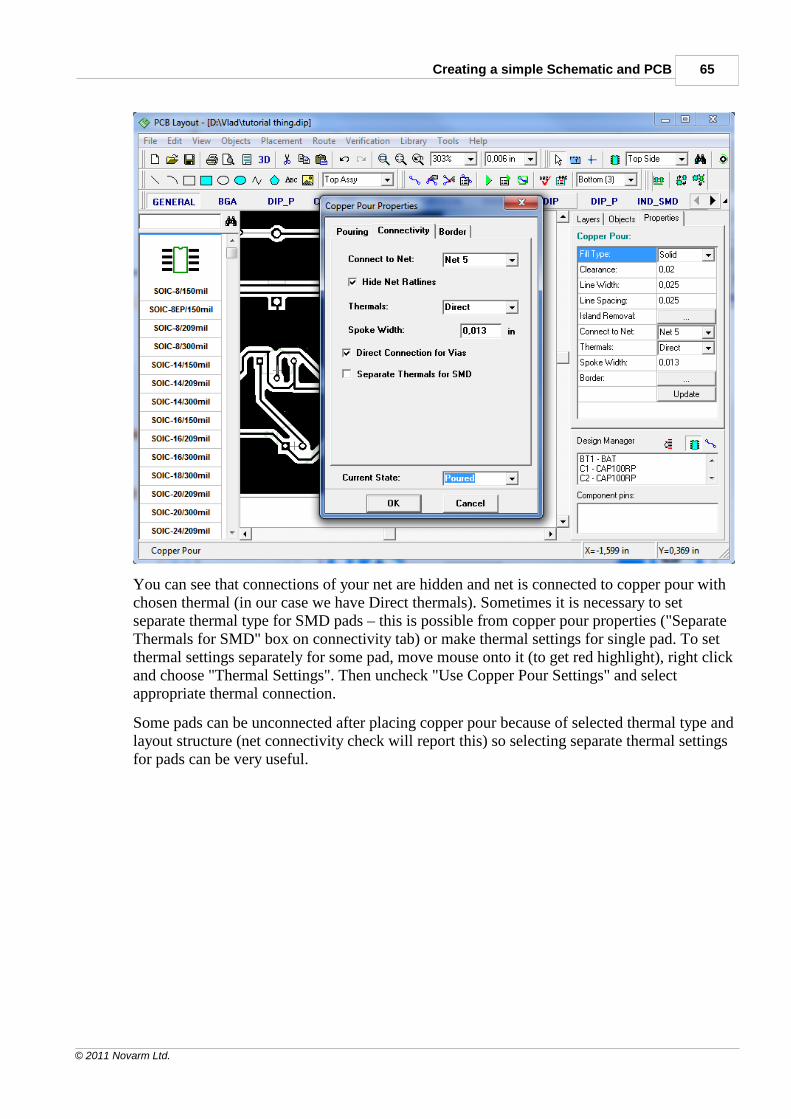
Now please unroute one of your nets: right click on the trace and "Unroute Net". Remembernet name (we unrouted "Net 5"). Right click on copper pour border and select "Properties", goto "Connectivity" tab. Select "Connect to Net: Net 5", check "Hide Net Ratlines" box, selectthermals, press OK to update copper pour.
Creating a simple Schematic and PCB 65
© 2011 Novarm Ltd.
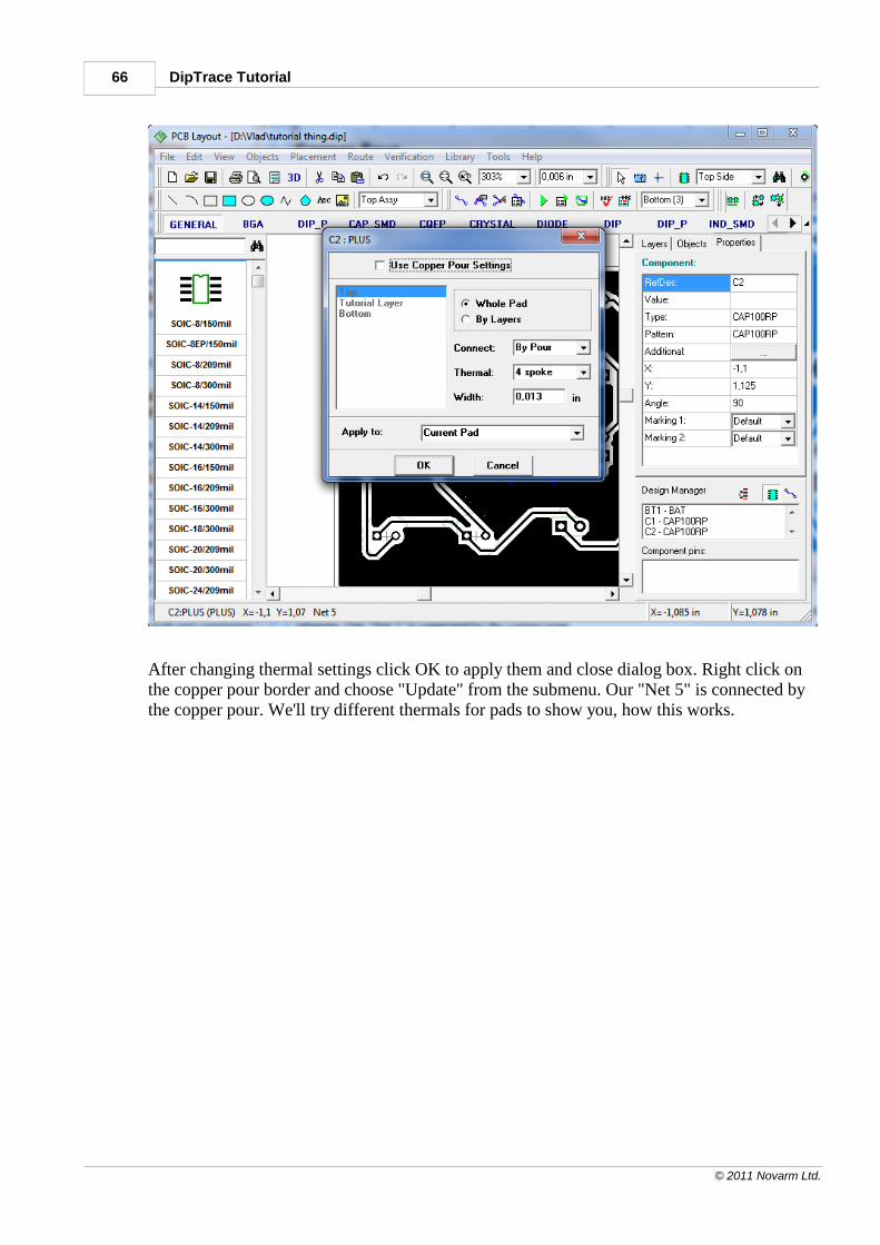
You can see that connections of your net are hidden and net is connected to copper pour withchosen thermal (in our case we have Direct thermals). Sometimes it is necessary to setseparate thermal type for SMD pads – this is possible from copper pour properties ("SeparateThermals for SMD" box on connectivity tab) or make thermal settings for single pad. To setthermal settings separately for some pad, move mouse onto it (to get red highlight), right clickand choose "Thermal Settings". Then uncheck "Use Copper Pour Settings" and selectappropriate thermal connection.
Some pads can be unconnected after placing copper pour because of selected thermal type andlayout structure (net connectivity check will report this) so selecting separate thermal settingsfor pads can be very useful.
DipTrace Tutorial66
© 2011 Novarm Ltd.
After changing thermal settings click OK to apply them and close dialog box. Right click onthe copper pour border and choose "Update" from the submenu. Our "Net 5" is connected bythe copper pour. We'll try different thermals for pads to show you, how this works.
Creating a simple Schematic and PCB 67
© 2011 Novarm Ltd.
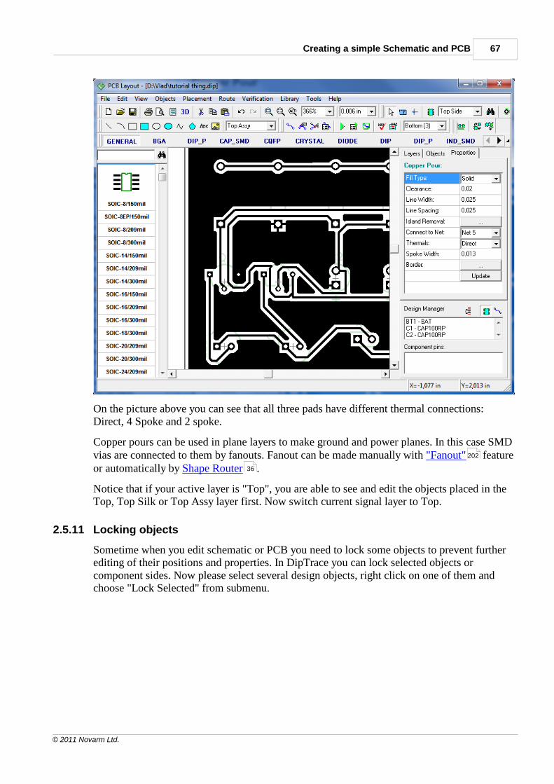
On the picture above you can see that all three pads have different thermal connections:Direct, 4 Spoke and 2 spoke.
Copper pours can be used in plane layers to make ground and power planes. In this case SMDvias are connected to them by fanouts. Fanout can be made manually with "Fanout" featureor automatically by Shape Router .
Notice that if your active layer is "Top", you are able to see and edit the objects placed in theTop, Top Silk or Top Assy layer first. Now switch current signal layer to Top.
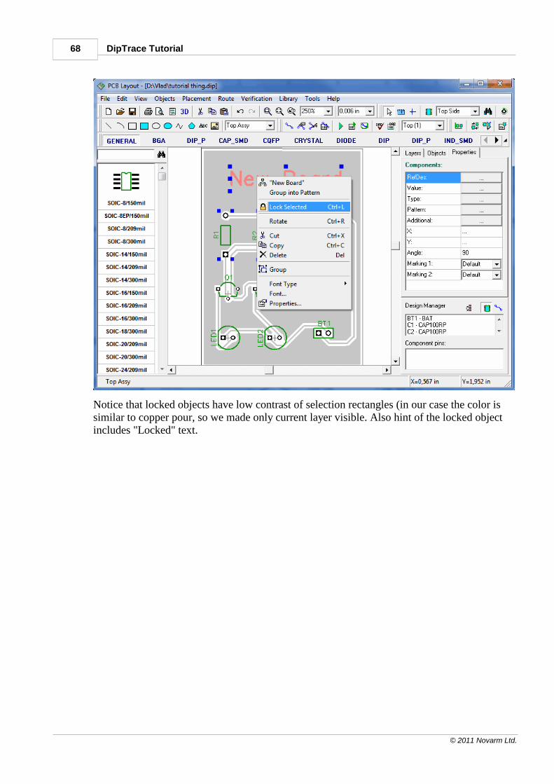
2.5.11 Locking objects
Sometime when you edit schematic or PCB you need to lock some objects to prevent furtherediting of their positions and properties. In DipTrace you can lock selected objects orcomponent sides. Now please select several design objects, right click on one of them andchoose "Lock Selected" from submenu.
202
36
DipTrace Tutorial68
© 2011 Novarm Ltd.
Notice that locked objects have low contrast of selection rectangles (in our case the color issimilar to copper pour, so we made only current layer visible. Also hint of the locked objectincludes "Locked" text.
Creating a simple Schematic and PCB 69
© 2011 Novarm Ltd.
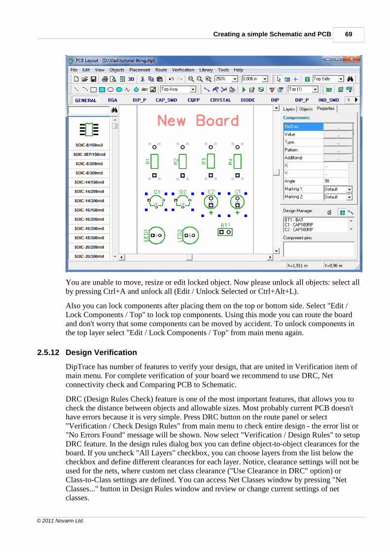
You are unable to move, resize or edit locked object. Now please unlock all objects: select allby pressing Ctrl+A and unlock all (Edit / Unlock Selected or Ctrl+Alt+L).
Also you can lock components after placing them on the top or bottom side. Select "Edit /Lock Components / Top" to lock top components. Using this mode you can route the boardand don't worry that some components can be moved by accident. To unlock components inthe top layer select "Edit / Lock Components / Top" from main menu again.
2.5.12 Design Verification
DipTrace has number of features to verify your design, that are united in Verification item ofmain menu. For complete verification of your board we recommend to use DRC, Netconnectivity check and Comparing PCB to Schematic.
DRC (Design Rules Check) feature is one of the most important features, that allows you tocheck the distance between objects and allowable sizes. Most probably current PCB doesn'thave errors because it is very simple. Press DRC button on the route panel or select"Verification / Check Design Rules" from main menu to check entire design - the error list or"No Errors Found" message will be shown. Now select "Verification / Design Rules" to setupDRC feature. In the design rules dialog box you can define object-to-object clearances for theboard. If you uncheck "All Layers" checkbox, you can choose layers from the list below thecheckbox and define different clearances for each layer. Notice, clearance settings will not beused for the nets, where custom net class clearance ("Use Clearance in DRC" option) orClass-to-Class settings are defined. You can access Net Classes window by pressing "NetClasses..." button in Design Rules window and review or change current settings of netclasses.

DipTrace Tutorial70
© 2011 Novarm Ltd.
We will check Class-to-Class Rules and Copper Pours, so please check corresponding boxesand press OK to apply changes and close window.
Now, lets try to see how DRC works. In previous subsections of this tutorial we created acopper pour on our PCB. Please check which layer is active now. In our case we have copperpour on the bottom layer. We press "B" hot key and bottom layer becomes active. We switchoff the grid with "F11" button and move some trace, until it touches the copper pour. Now goto "Verification / Check Design Rules" or just press "F9" to run the DRC. Window with thelist of errors will pop up.
In drop down list of this window we can select to show errors by layer.
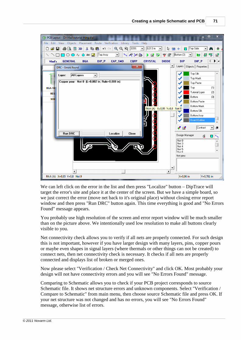
Creating a simple Schematic and PCB 71
© 2011 Novarm Ltd.
We can left click on the error in the list and then press "Localize" button – DipTrace willtarget the error's site and place it at the center of the screen. But we have a simple board, sowe just correct the error (move net back to it's original place) without closing error reportwindow and then press "Run DRC" button again. This time everything is good and "No ErrorsFound" message appears.
You probably use high resolution of the screen and error report window will be much smallerthan on the picture above. We intentionally used low resolution to make all buttons clearlyvisible to you.
Net connectivity check allows you to verify if all nets are properly connected. For such designthis is not important, however if you have larger design with many layers, pins, copper poursor maybe even shapes in signal layers (where thermals or other things can not be created) toconnect nets, then net connectivity check is necessary. It checks if all nets are properlyconnected and displays list of broken or merged ones.
Now please select "Verification / Check Net Connectivity" and click OK. Most probably yourdesign will not have connectivity errors and you will see "No Errors Found" message.
Comparing to Schematic allows you to check if your PCB project corresponds to sourceSchematic file. It shows net structure errors and unknown components. Select "Verification /Compare to Schematic" from main menu, then choose source Schematic file and press OK. Ifyour net structure was not changed and has no errors, you will see "No Errors Found"message, otherwise list of errors.
DipTrace Tutorial72
© 2011 Novarm Ltd.
Net connectivity check and Comparing to Schematic works in the same way as DRC and youcan select errors from a list to highlight them.
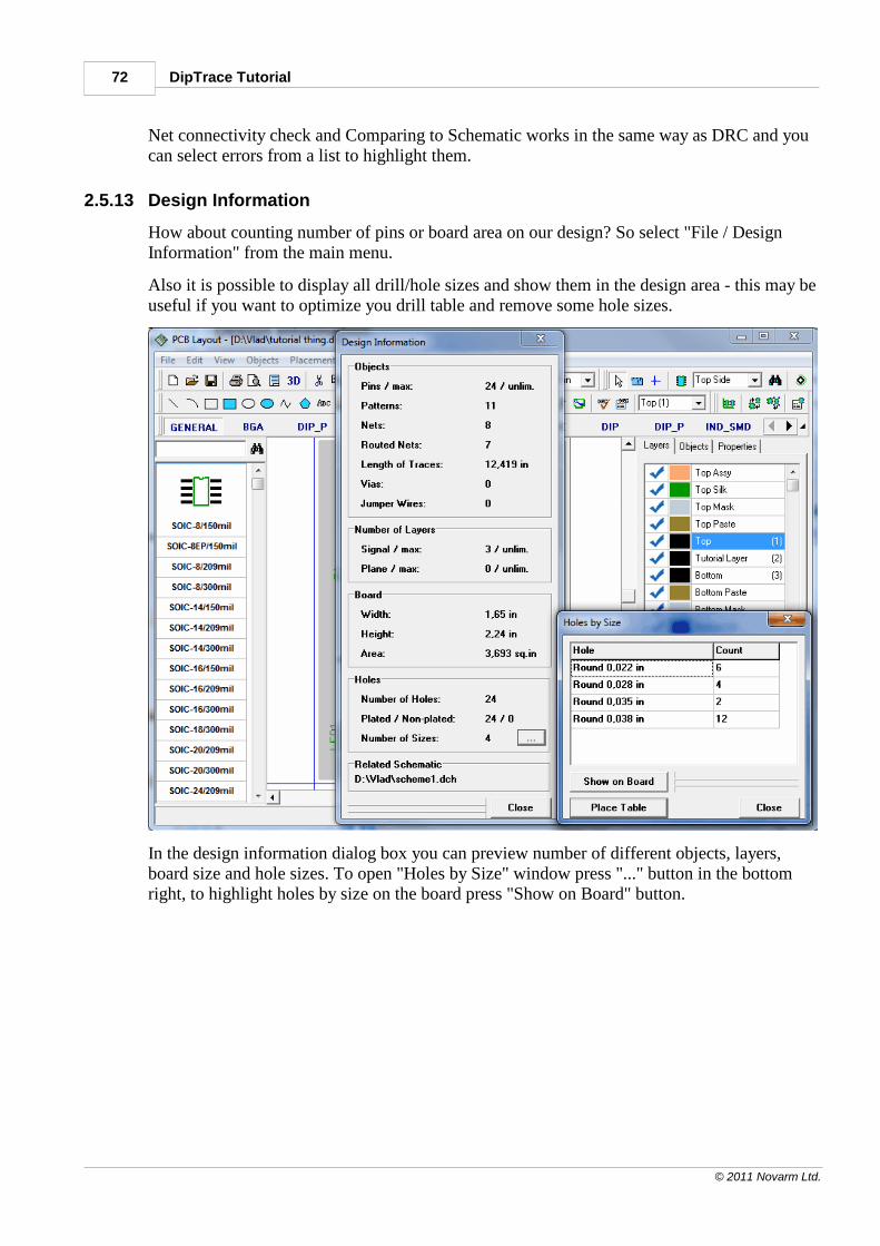
2.5.13 Design Information
How about counting number of pins or board area on our design? So select "File / DesignInformation" from the main menu.
Also it is possible to display all drill/hole sizes and show them in the design area - this may beuseful if you want to optimize you drill table and remove some hole sizes.
In the design information dialog box you can preview number of different objects, layers,board size and hole sizes. To open "Holes by Size" window press "..." button in the bottomright, to highlight holes by size on the board press "Show on Board" button.
Creating a simple Schematic and PCB 73
© 2011 Novarm Ltd.
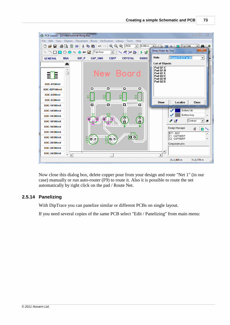
Now close this dialog box, delete copper pour from your design and route "Net 1" (in ourcase) manually or run auto-router (F9) to route it. Also it is possible to route the netautomatically by right click on the pad / Route Net.
2.5.14 Panelizing
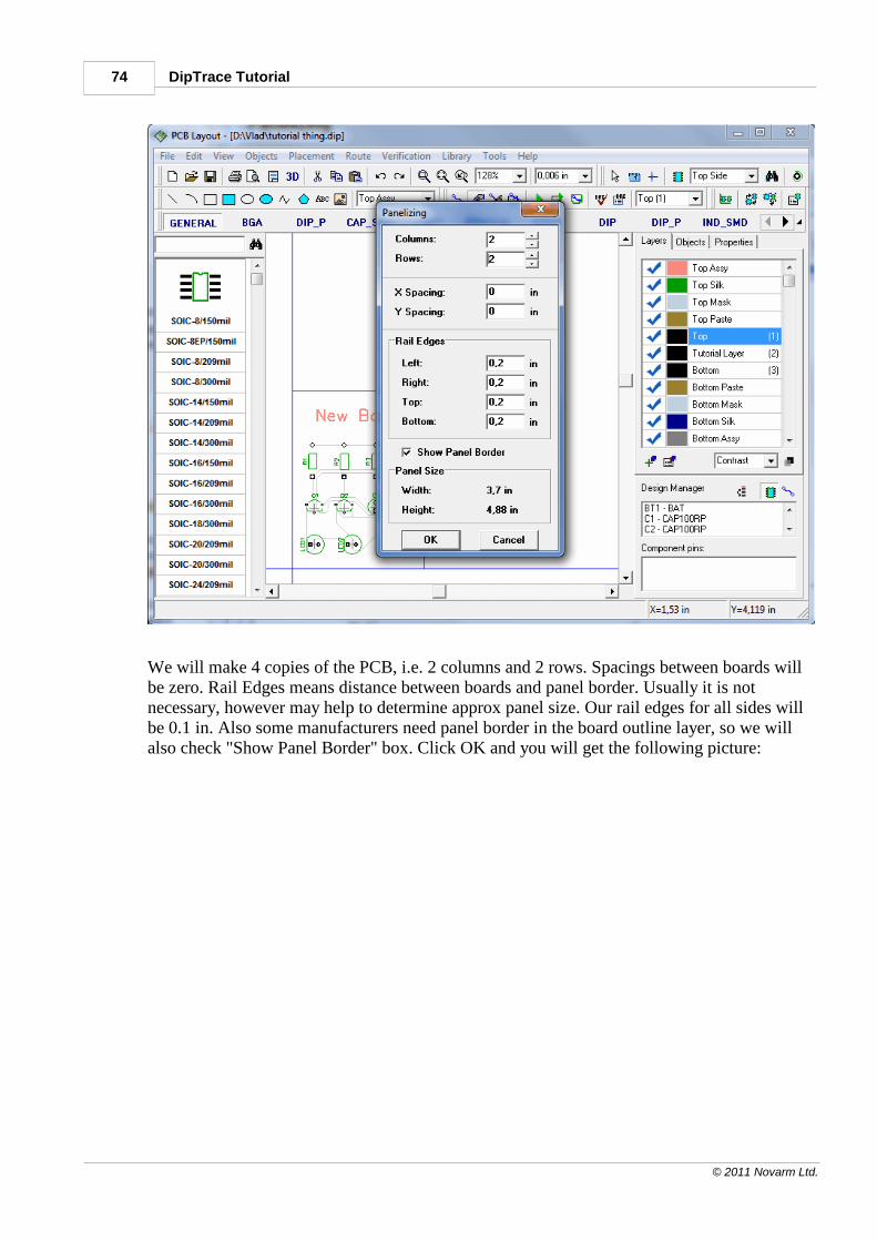
With DipTrace you can panelize similar or different PCBs on single layout.
If you need several copies of the same PCB select "Edit / Panelizing" from main menu:
DipTrace Tutorial74
© 2011 Novarm Ltd.
We will make 4 copies of the PCB, i.e. 2 columns and 2 rows. Spacings between boards willbe zero. Rail Edges means distance between boards and panel border. Usually it is notnecessary, however may help to determine approx panel size. Our rail edges for all sides willbe 0.1 in. Also some manufacturers need panel border in the board outline layer, so we willalso check "Show Panel Border" box. Click OK and you will get the following picture:
Creating a simple Schematic and PCB 75
© 2011 Novarm Ltd.
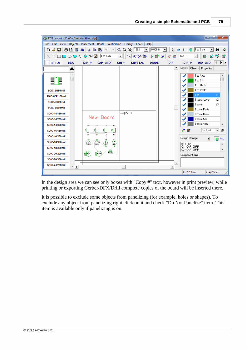
In the design area we can see only boxes with "Copy #" text, however in print preview, whileprinting or exporting Gerber/DFX/Drill complete copies of the board will be inserted there.
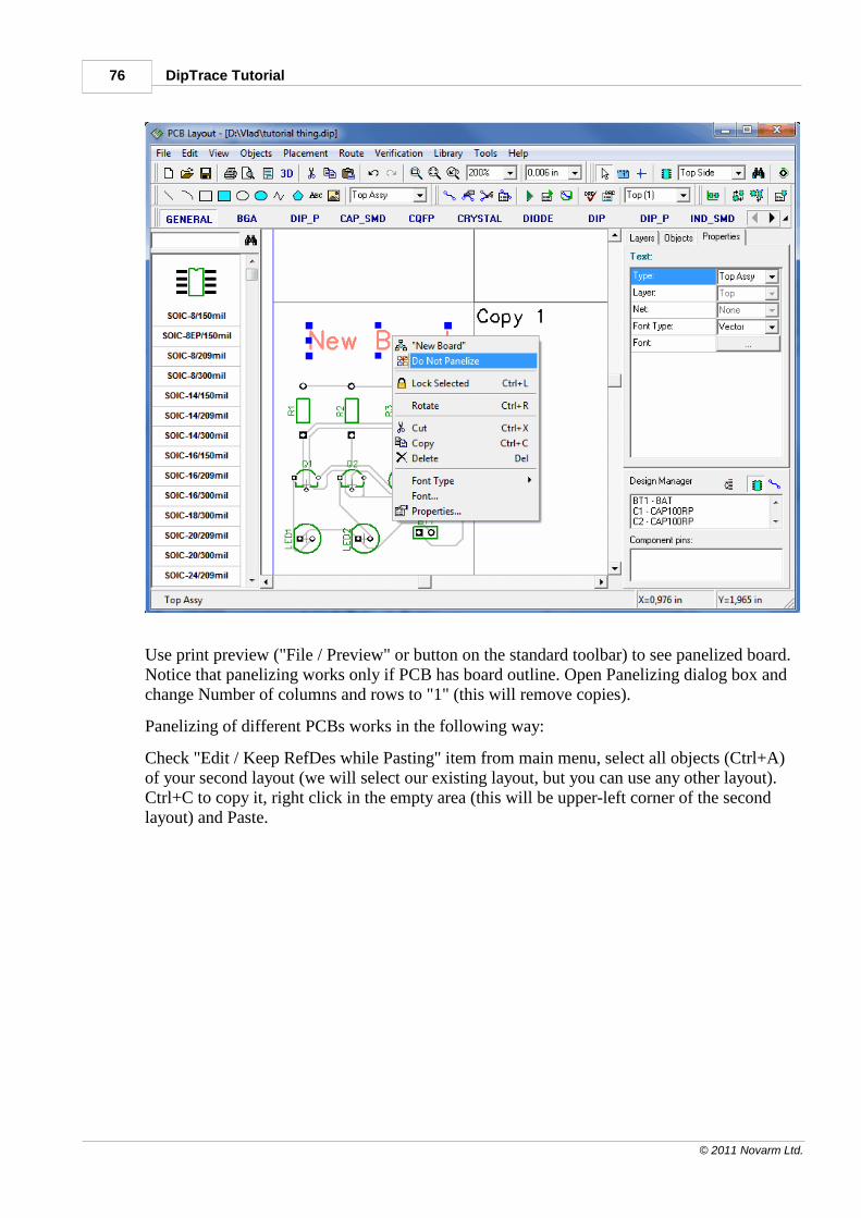
It is possible to exclude some objects from panelizing (for example, holes or shapes). Toexclude any object from panelizing right click on it and check "Do Not Panelize" item. Thisitem is available only if panelizing is on.
DipTrace Tutorial76
© 2011 Novarm Ltd.
Use print preview ("File / Preview" or button on the standard toolbar) to see panelized board.Notice that panelizing works only if PCB has board outline. Open Panelizing dialog box andchange Number of columns and rows to "1" (this will remove copies).
Panelizing of different PCBs works in the following way:
Check "Edit / Keep RefDes while Pasting" item from main menu, select all objects (Ctrl+A)of your second layout (we will select our existing layout, but you can use any other layout).Ctrl+C to copy it, right click in the empty area (this will be upper-left corner of the secondlayout) and Paste.
Creating a simple Schematic and PCB 77
© 2011 Novarm Ltd.
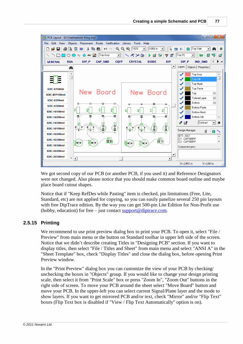
We got second copy of our PCB (or another PCB, if you used it) and Reference Designatorswere not changed. Also please notice that you should make common board outline and maybeplace board cutout shapes.
Notice that if "Keep RefDes while Pasting" item is checked, pin limitations (Free, Lite,Standard, etc) are not applied for copying, so you can easily panelize several 250 pin layoutswith free DipTrace edition. By the way you can get 500-pin Lite Edition for Non-Profit use(hobby, education) for free – just contact [email protected].
2.5.15 Printing
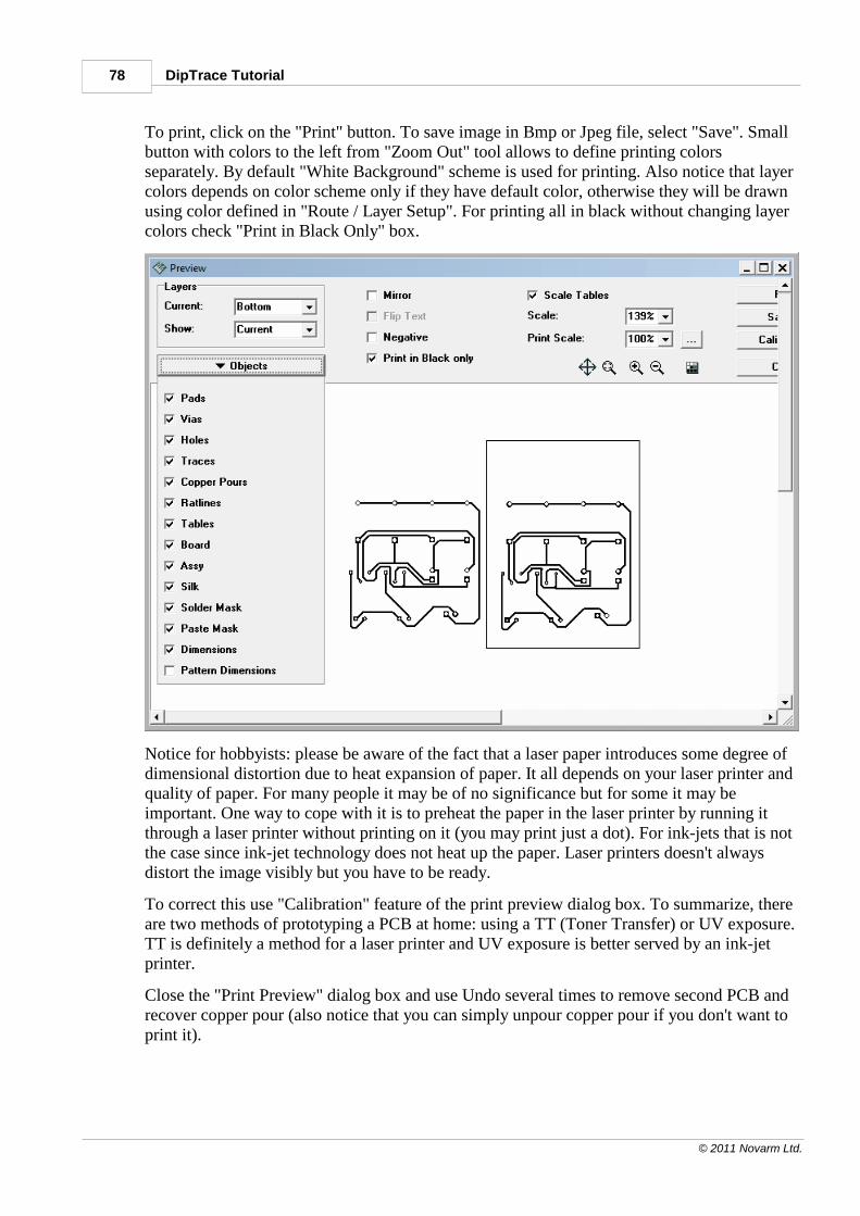
We recommend to use print preview dialog box to print your PCB. To open it, select "File /Preview" from main menu or the button on Standard toolbar in upper left side of the screen.Notice that we didn’t describe creating Titles in "Designing PCB" section. If you want todisplay titles, then select "File / Titles and Sheet" from main menu and select "ANSI A" in the"Sheet Template" box, check "Display Titles" and close the dialog box, before opening PrintPreview window.
In the "Print Preview" dialog box you can customize the view of your PCB by checking/unchecking the boxes in "Objects" group. If you would like to change your design printingscale, then select it from "Print Scale" box or press "Zoom In", "Zoom Out" buttons in theright side of screen. To move your PCB around the sheet select "Move Board" button andmove your PCB. In the upper-left you can select current Signal/Plane layer and the mode toshow layers. If you want to get mirrored PCB and/or text, check "Mirror" and/or "Flip Text"boxes (Flip Text box is disabled if "View / Flip Text Automatically" option is on).
DipTrace Tutorial78
© 2011 Novarm Ltd.
To print, click on the "Print" button. To save image in Bmp or Jpeg file, select "Save". Smallbutton with colors to the left from "Zoom Out" tool allows to define printing colorsseparately. By default "White Background" scheme is used for printing. Also notice that layercolors depends on color scheme only if they have default color, otherwise they will be drawnusing color defined in "Route / Layer Setup". For printing all in black without changing layercolors check "Print in Black Only" box.
Notice for hobbyists: please be aware of the fact that a laser paper introduces some degree ofdimensional distortion due to heat expansion of paper. It all depends on your laser printer andquality of paper. For many people it may be of no significance but for some it may beimportant. One way to cope with it is to preheat the paper in the laser printer by running itthrough a laser printer without printing on it (you may print just a dot). For ink-jets that is notthe case since ink-jet technology does not heat up the paper. Laser printers doesn't alwaysdistort the image visibly but you have to be ready.
To correct this use "Calibration" feature of the print preview dialog box. To summarize, thereare two methods of prototyping a PCB at home: using a TT (Toner Transfer) or UV exposure.TT is definitely a method for a laser printer and UV exposure is better served by an ink-jetprinter.
Close the "Print Preview" dialog box and use Undo several times to remove second PCB andrecover copper pour (also notice that you can simply unpour copper pour if you don't want toprint it).
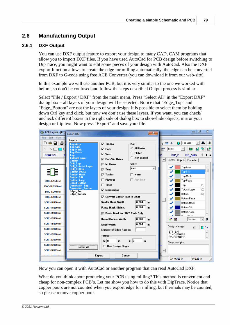
Creating a simple Schematic and PCB 79
© 2011 Novarm Ltd.
2.6 Manufacturing Output
2.6.1 DXF Output
You can use DXF output feature to export your design to many CAD, CAM programs thatallow you to import DXF files. If you have used AutoCad for PCB design before switching toDipTrace, you might want to edit some pieces of your design with AutoCad. Also the DXFexport function allows to create the edge for milling automatically, the edge can be convertedfrom DXF to G-code using free ACE Converter (you can download it from our web-site).
In this example we will use another PCB, but it is very similar to the one we worked withbefore, so don't be confused and follow the steps described.Output process is similar.
Select "File / Export / DXF" from the main menu. Press "Select All" in the "Export DXF"dialog box – all layers of your design will be selected. Notice that "Edge_Top" and"Edge_Bottom" are not the layers of your design. It is possible to select them by holdingdown Ctrl key and click, but now we don’t use these layers. If you want, you can check/uncheck different boxes in the right side of dialog box to show/hide objects, mirror yourdesign or flip text. Now press "Export" and save your file.
Now you can open it with AutoCad or another program that can read AutoCad DXF.
What do you think about producing your PCB using milling? This method is convenient andcheap for non-complex PCB’s. Let me show you how to do this with DipTrace. Notice thatcopper pours are not counted when you export edge for milling, but thermals may be counted,so please remove copper pour.
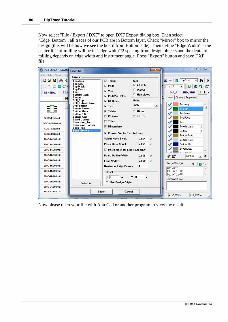
DipTrace Tutorial80
© 2011 Novarm Ltd.
Now select "File / Export / DXF" to open DXF Export dialog box. Then select"Edge_Bottom", all traces of our PCB are in Bottom layer. Check "Mirror" box to mirror thedesign (this will be how we see the board from Bottom side). Then define "Edge Width" – thecenter line of milling will be in "edge width"/2 spacing from design objects and the depth ofmilling depends on edge width and instrument angle. Press "Export" button and save DXFfile.
Now please open your file with AutoCad or another program to view the result:
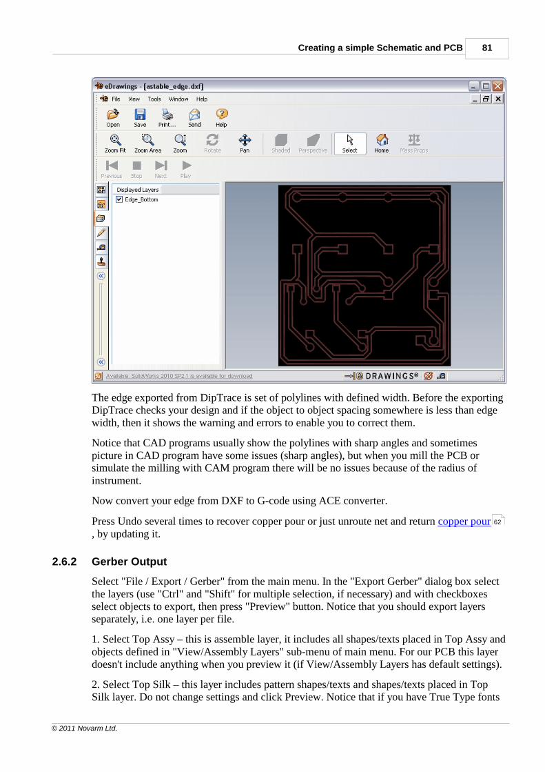
Creating a simple Schematic and PCB 81
© 2011 Novarm Ltd.
The edge exported from DipTrace is set of polylines with defined width. Before the exportingDipTrace checks your design and if the object to object spacing somewhere is less than edgewidth, then it shows the warning and errors to enable you to correct them.
Notice that CAD programs usually show the polylines with sharp angles and sometimespicture in CAD program have some issues (sharp angles), but when you mill the PCB orsimulate the milling with CAM program there will be no issues because of the radius ofinstrument.
Now convert your edge from DXF to G-code using ACE converter.
Press Undo several times to recover copper pour or just unroute net and return copper pour, by updating it.
2.6.2 Gerber Output
Select "File / Export / Gerber" from the main menu. In the "Export Gerber" dialog box selectthe layers (use "Ctrl" and "Shift" for multiple selection, if necessary) and with checkboxesselect objects to export, then press "Preview" button. Notice that you should export layersseparately, i.e. one layer per file.
1. Select Top Assy – this is assemble layer, it includes all shapes/texts placed in Top Assy andobjects defined in "View/Assembly Layers" sub-menu of main menu. For our PCB this layerdoesn't include anything when you preview it (if View/Assembly Layers has default settings).
2. Select Top Silk – this layer includes pattern shapes/texts and shapes/texts placed in TopSilk layer. Do not change settings and click Preview. Notice that if you have True Type fonts
62
DipTrace Tutorial82
© 2011 Novarm Ltd.
and can not see texts or they are displayed incompletely (depends on font and its size), youshould simply make "Recognize Accuracy" value a bit smaller (do not make it minimumpossible).
3. Top Mask – this is solder mask layer. It is generated automatically based on pads, theirsettings and common "Solder Mask Swell" defined in Gerber dialog box + includes shapesplaced in solder mask layer. I suppose we should only uncheck "Vias" box, as they are usuallycovered with the solder mask. To change custom solder mask settings for pads right click onthe pad and select "Mask / Paste Settings" from its submenu.
4. Top Paste – this layer is usually used for SMT pads only, so we can check "Paste Mask forSMT Pads only".
5. Signal layers (Top, Bottom, etc.) - these are our copper layers, now please check "Vias"box for all of them and preview if all layers are displayed correctly. Notice that if you plan todrill holes manually you can also check "Pad/Via Holes" box, however this option is notrecommended if you send files to manufacturer. Also notice that in case that "Pad/Via Holes"box is checked, 2 layers will be created for each signal layer if there are through pads or vias:drawing and clearing. The second layer is used to remove artefacts over the drill holes.
6. Bottom Paste – Bottom Assy, by default all text objects in Bottom layers are flipped –"View / Flip Text Automatically" option in main menu, however if that option is off, you canflip text manually for the layers you want ("Flip Text" box).
7. Board outline includes board outline only with defined width. Board layer includes boardas filled polygon.
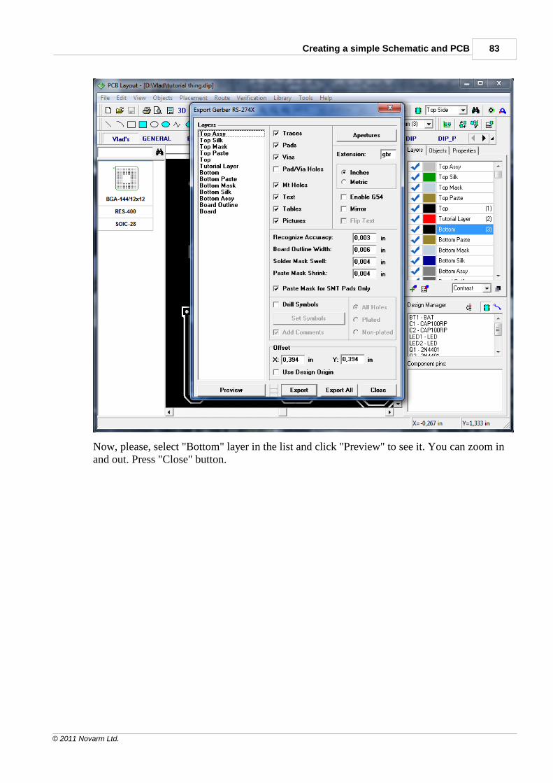
Creating a simple Schematic and PCB 83
© 2011 Novarm Ltd.
Now, please, select "Bottom" layer in the list and click "Preview" to see it. You can zoom inand out. Press "Close" button.
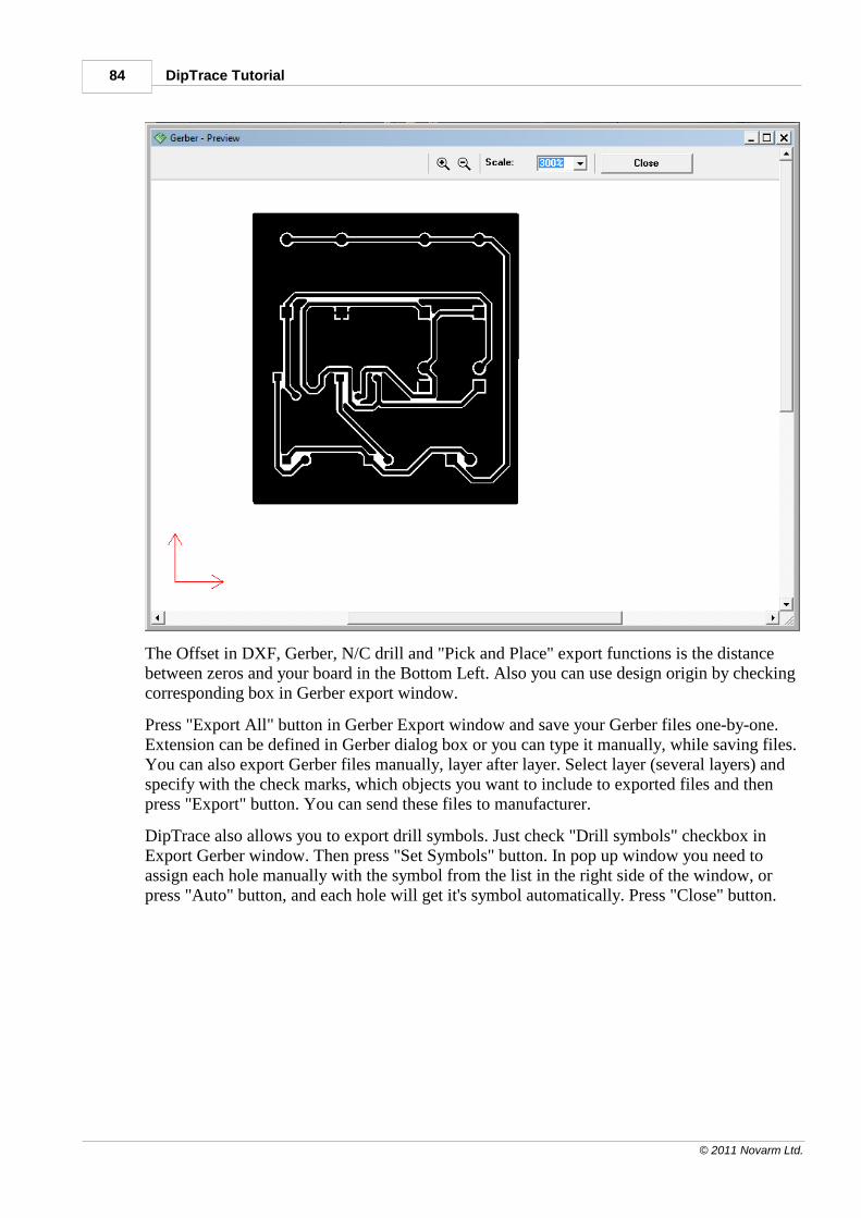
DipTrace Tutorial84
© 2011 Novarm Ltd.
The Offset in DXF, Gerber, N/C drill and "Pick and Place" export functions is the distancebetween zeros and your board in the Bottom Left. Also you can use design origin by checkingcorresponding box in Gerber export window.
Press "Export All" button in Gerber Export window and save your Gerber files one-by-one.Extension can be defined in Gerber dialog box or you can type it manually, while saving files.You can also export Gerber files manually, layer after layer. Select layer (several layers) andspecify with the check marks, which objects you want to include to exported files and thenpress "Export" button. You can send these files to manufacturer.
DipTrace also allows you to export drill symbols. Just check "Drill symbols" checkbox inExport Gerber window. Then press "Set Symbols" button. In pop up window you need toassign each hole manually with the symbol from the list in the right side of the window, orpress "Auto" button, and each hole will get it's symbol automatically. Press "Close" button.
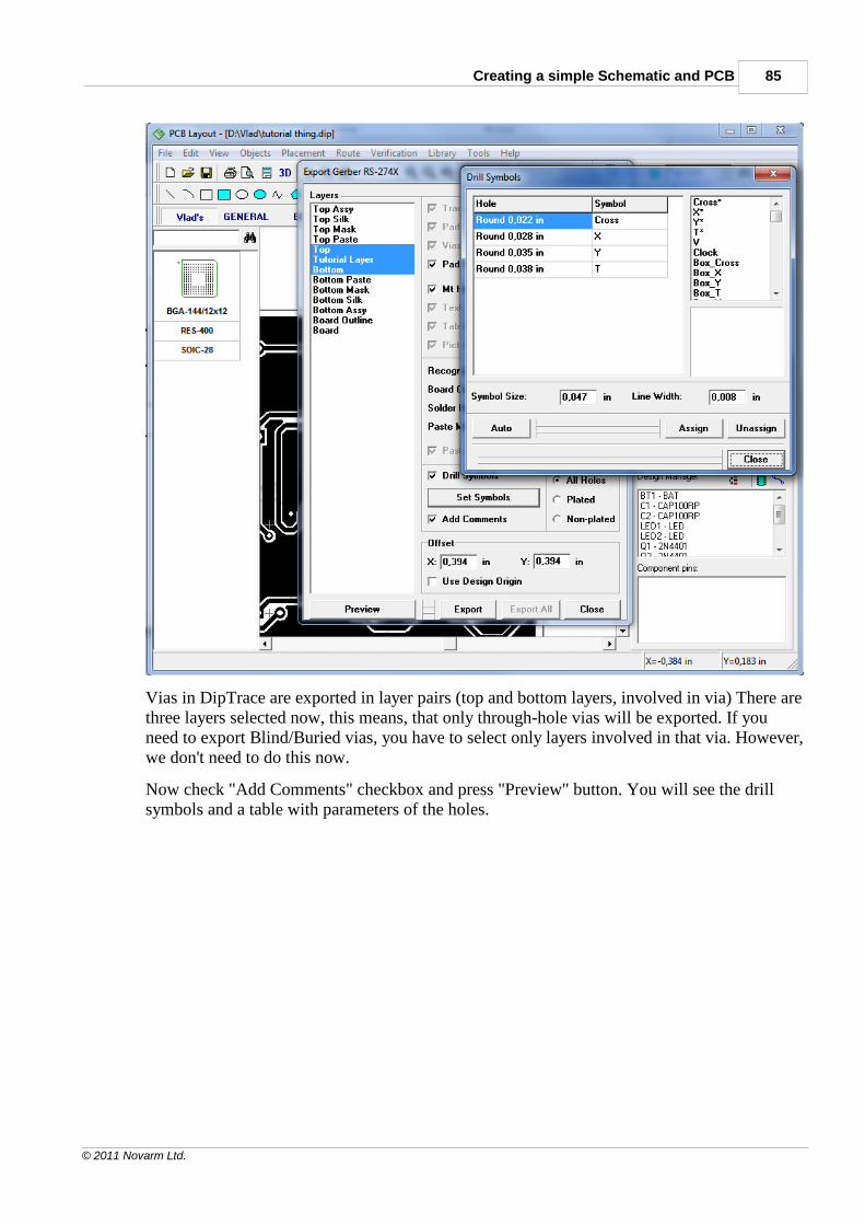
Creating a simple Schematic and PCB 85
© 2011 Novarm Ltd.
Vias in DipTrace are exported in layer pairs (top and bottom layers, involved in via) There arethree layers selected now, this means, that only through-hole vias will be exported. If youneed to export Blind/Buried vias, you have to select only layers involved in that via. However,we don't need to do this now.
Now check "Add Comments" checkbox and press "Preview" button. You will see the drillsymbols and a table with parameters of the holes.
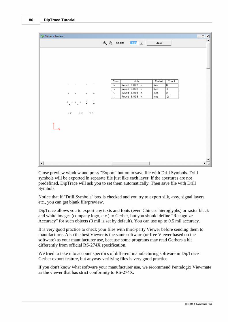
DipTrace Tutorial86
© 2011 Novarm Ltd.
Close preview window and press "Export" button to save file with Drill Symbols. Drillsymbols will be exported in separate file just like each layer. If the apertures are notpredefined, DipTrace will ask you to set them automatically. Then save file with DrillSymbols.
Notice that if "Drill Symbols" box is checked and you try to export silk, assy, signal layers,etc., you can get blank file/preview.
DipTrace allows you to export any texts and fonts (even Chinese hieroglyphs) or raster blackand white images (company logo, etc.) to Gerber, but you should define “RecognizeAccuracy” for such objects (3 mil is set by default). You can use up to 0.5 mil accuracy.
It is very good practice to check your files with third-party Viewer before sending them tomanufacturer. Also the best Viewer is the same software (or free Viewer based on thesoftware) as your manufacturer use, because some programs may read Gerbers a bitdifferently from official RS-274X specification.
We tried to take into account specifics of different manufacturing software in DipTraceGerber export feature, but anyway verifying files is very good practice.
If you don't know what software your manufacturer use, we recommend Pentalogix Viewmateas the viewer that has strict conformity to RS-274X.
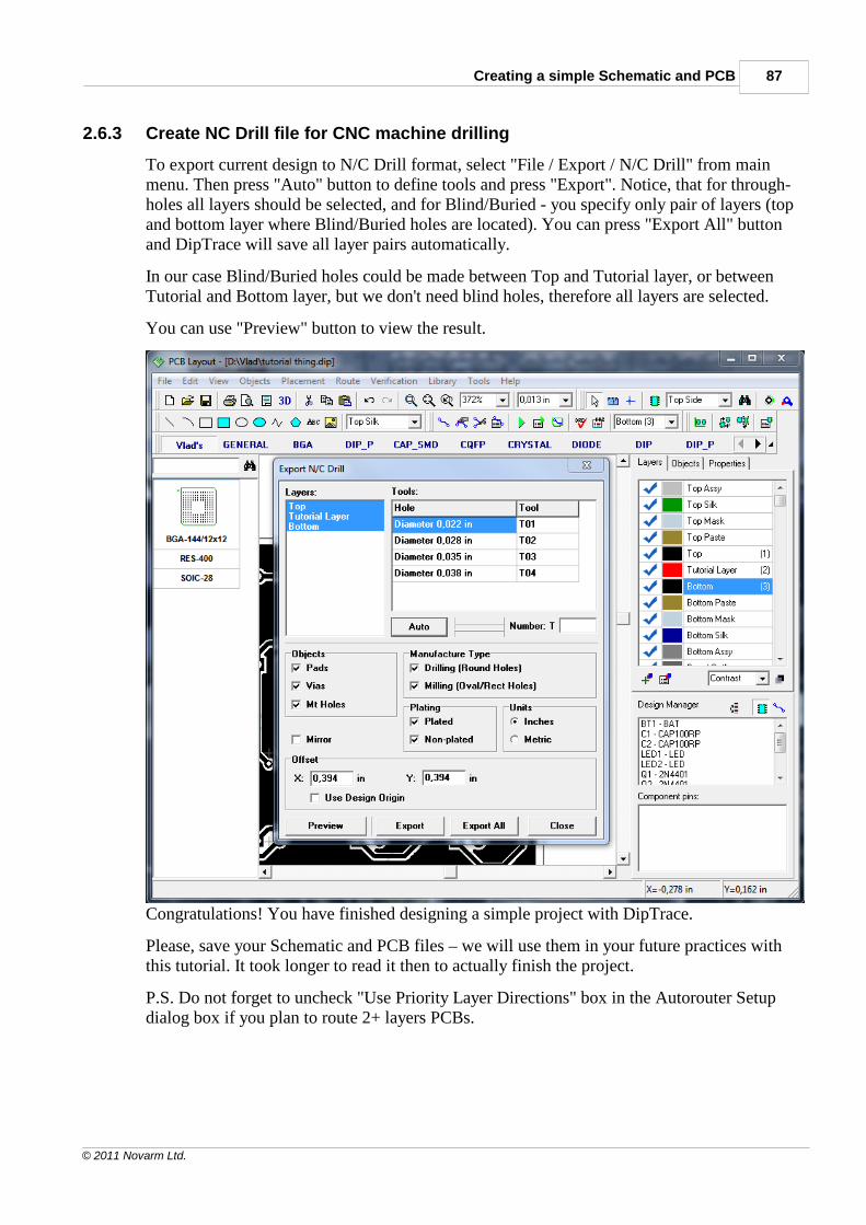
Creating a simple Schematic and PCB 87
© 2011 Novarm Ltd.
2.6.3 Create NC Drill file for CNC machine drilling
To export current design to N/C Drill format, select "File / Export / N/C Drill" from mainmenu. Then press "Auto" button to define tools and press "Export". Notice, that for through-holes all layers should be selected, and for Blind/Buried - you specify only pair of layers (topand bottom layer where Blind/Buried holes are located). You can press "Export All" buttonand DipTrace will save all layer pairs automatically.
In our case Blind/Buried holes could be made between Top and Tutorial layer, or betweenTutorial and Bottom layer, but we don't need blind holes, therefore all layers are selected.
You can use "Preview" button to view the result.
Congratulations! You have finished designing a simple project with DipTrace.
Please, save your Schematic and PCB files – we will use them in your future practices withthis tutorial. It took longer to read it then to actually finish the project.
P.S. Do not forget to uncheck "Use Priority Layer Directions" box in the Autorouter Setupdialog box if you plan to route 2+ layers PCBs.
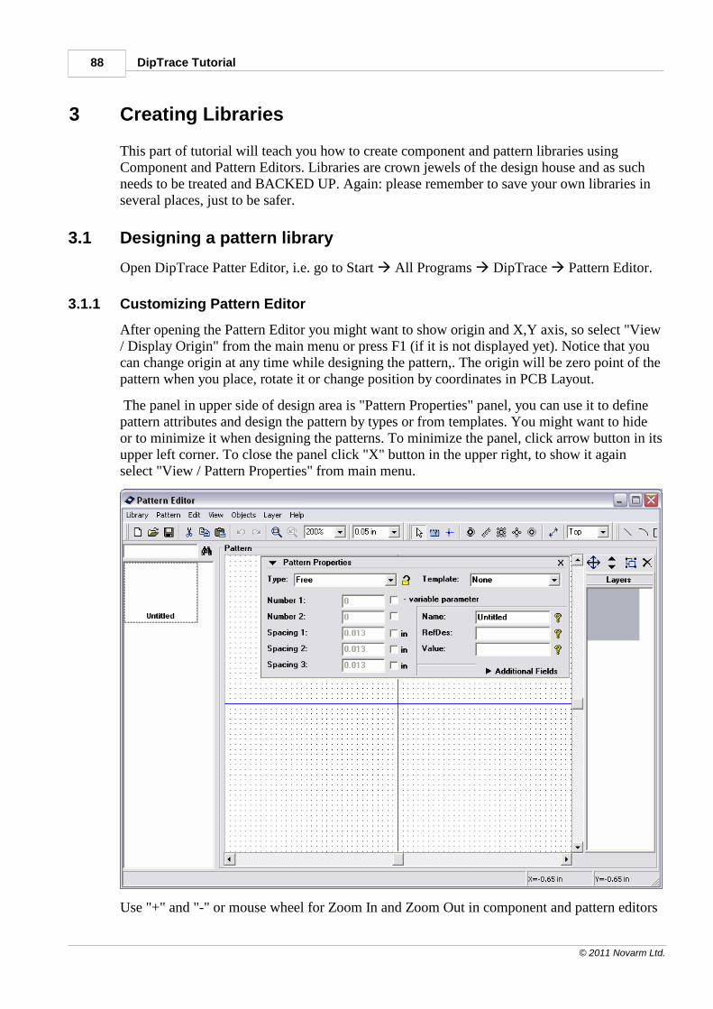
DipTrace Tutorial88
© 2011 Novarm Ltd.
3 Creating Libraries
This part of tutorial will teach you how to create component and pattern libraries usingComponent and Pattern Editors. Libraries are crown jewels of the design house and as suchneeds to be treated and BACKED UP. Again: please remember to save your own libraries inseveral places, just to be safer.
3.1 Designing a pattern library
Open DipTrace Patter Editor, i.e. go to Start All Programs DipTrace Pattern Editor.
3.1.1 Customizing Pattern Editor
After opening the Pattern Editor you might want to show origin and X,Y axis, so select "View/ Display Origin" from the main menu or press F1 (if it is not displayed yet). Notice that youcan change origin at any time while designing the pattern,. The origin will be zero point of thepattern when you place, rotate it or change position by coordinates in PCB Layout.
The panel in upper side of design area is "Pattern Properties" panel, you can use it to definepattern attributes and design the pattern by types or from templates. You might want to hideor to minimize it when designing the patterns. To minimize the panel, click arrow button in itsupper left corner. To close the panel click "X" button in the upper right, to show it againselect "View / Pattern Properties" from main menu.
Use "+" and "-" or mouse wheel for Zoom In and Zoom Out in component and pattern editors
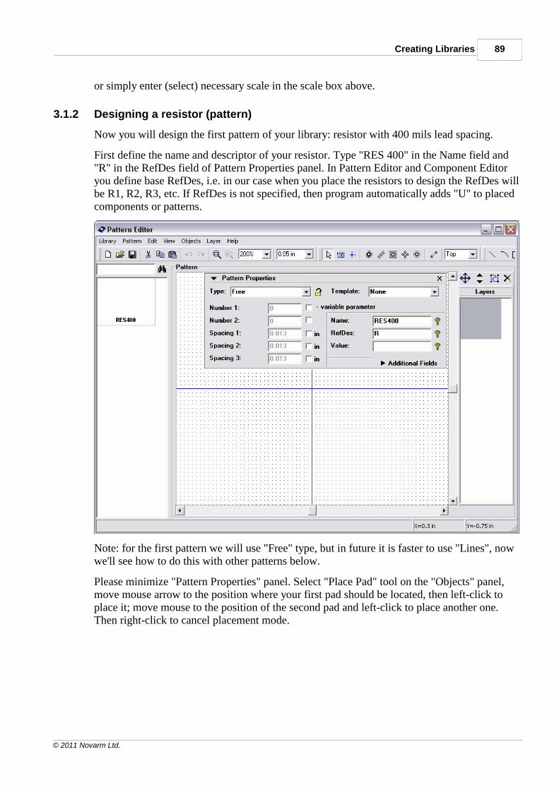
Creating Libraries 89
© 2011 Novarm Ltd.
or simply enter (select) necessary scale in the scale box above.
3.1.2 Designing a resistor (pattern)
Now you will design the first pattern of your library: resistor with 400 mils lead spacing.
First define the name and descriptor of your resistor. Type "RES 400" in the Name field and"R" in the RefDes field of Pattern Properties panel. In Pattern Editor and Component Editoryou define base RefDes, i.e. in our case when you place the resistors to design the RefDes willbe R1, R2, R3, etc. If RefDes is not specified, then program automatically adds "U" to placedcomponents or patterns.
Note: for the first pattern we will use "Free" type, but in future it is faster to use "Lines", nowwe'll see how to do this with other patterns below.
Please minimize "Pattern Properties" panel. Select "Place Pad" tool on the "Objects" panel,move mouse arrow to the position where your first pad should be located, then left-click toplace it; move mouse to the position of the second pad and left-click to place another one.Then right-click to cancel placement mode.
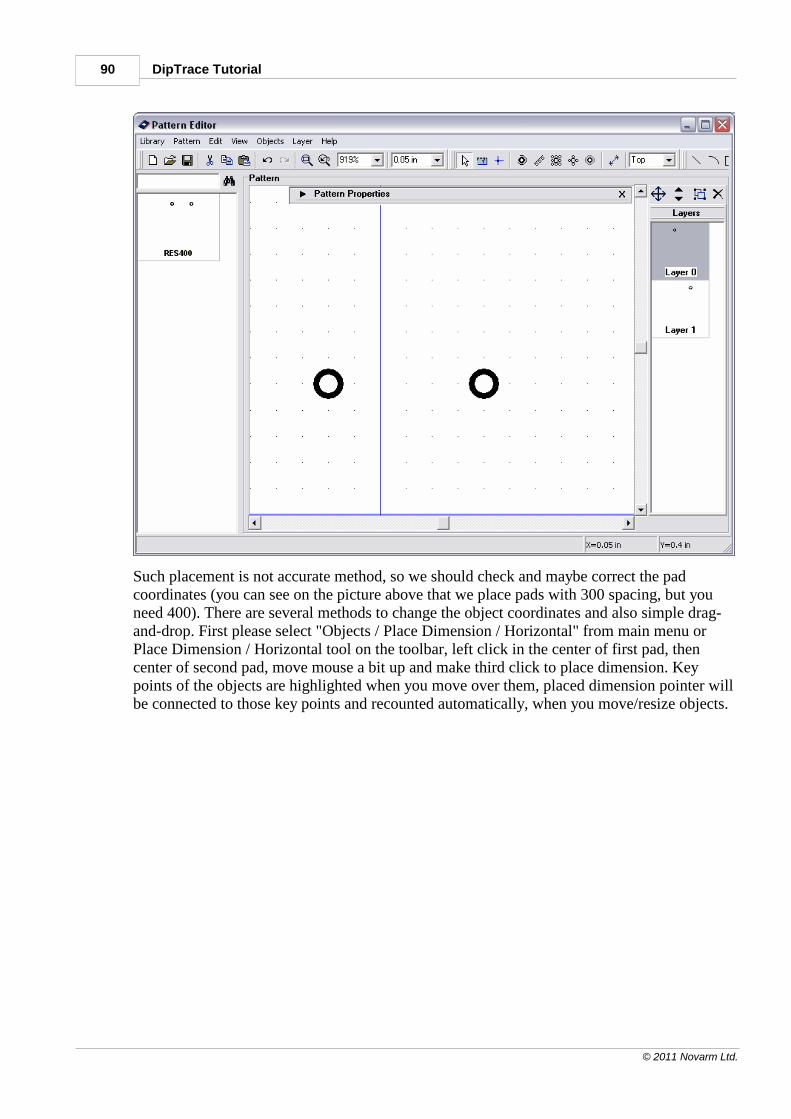
DipTrace Tutorial90
© 2011 Novarm Ltd.
Such placement is not accurate method, so we should check and maybe correct the padcoordinates (you can see on the picture above that we place pads with 300 spacing, but youneed 400). There are several methods to change the object coordinates and also simple drag-and-drop. First please select "Objects / Place Dimension / Horizontal" from main menu orPlace Dimension / Horizontal tool on the toolbar, left click in the center of first pad, thencenter of second pad, move mouse a bit up and make third click to place dimension. Keypoints of the objects are highlighted when you move over them, placed dimension pointer willbe connected to those key points and recounted automatically, when you move/resize objects.
Creating Libraries 91
© 2011 Novarm Ltd.
Also you can change properties of dimension (Layer, Units, Arrow Size) by right click on itand selecting Properties in the submenu.
Now we will use "Layer Objects" dialog box. In the right side of screen you can see the layers.Notice that those are only logical layers for editing (not signal or silk layers). Now select thelayers: move mouse arrow over the "Layer 0", hold down the left mouse button, move cursorto "Layer 1", then release mouse button. Select "Layer / Merge Layers" or the correspondingbutton in the upper part of layers panel to your right. You have made a single layer with twopads in it; double click on it to open "Layer Objects" dialog box.
Select the pad with incorrect coordinates and change X to make 400 mils distance betweenpads, then click "Close" button to close the dialog box.
DipTrace Tutorial92
© 2011 Novarm Ltd.
You can see that dimension object was recounted automatically and now displays correctdistance value.
You might want to change the pad settings, i.e. shape, size, hole shape and diameter, SMD orThrough hole type, etc. Pattern has pad settings by default, that can be applied to all its padsand also each pad may have its own settings. To change the settings by default for the patternselect "Pattern / Pad Properties" from main menu. In the "Pad Properties" dialog box you canchange the shape of your pad: Ellipse, Oval, Rectangle or Polygon (click Points to define thenumber of vertices or point coordinates for polygonal pad). You can make round or oval holesin pads, define hole diameter (it is applied to "Through" pads only). Also you can use padtemplate by selecting it from "Template" box. To create your own templates click "…>>"button – that will open template manager. All templates you make here can be used for fastchange of pad settings in different dialog boxes of Pattern Editor and PCB Layout.
Creating Libraries 93
© 2011 Novarm Ltd.
Please close "Templates", change shape to "Rectangle", width to "0.08", and Type to"Surface", then click OK to apply changes.
DipTrace Tutorial94
© 2011 Novarm Ltd.
Notice that for surface pads you can also change side, i.e. place them on the bottom side (theywill be on top when component is placed to the bottom side in PCB Layout).To change sideselect pad(s), right click on one of them and select "Change Side". Current side for placingnew pads and shapes can be also selected on the objects panel (box with "Top" text in theright side).
Now you will change the settings of single pad. Move the mouse arrow over first pad, right-click, select "Properties" (If the pad is not highlighted while moving mouse arrow over it,right-click or use "Default Mode" button in the upper side of screen or right click in the emptyarea to switch to default mode).
In the Pad Properties dialog box uncheck "Default for Pattern" box to enable the pad’s ownsettings, change shape to "Polygon", width and height to "0.09", then press "Points" to open"Polygon Points" dialog box. Here you can define the type of polygonal pad and if non-regular, polygon point coordinates. Close the "Polygon Points" dialog box, then change holediameter to "0,04", On Board to "Through" and press OK to close the dialog box and applychanges.
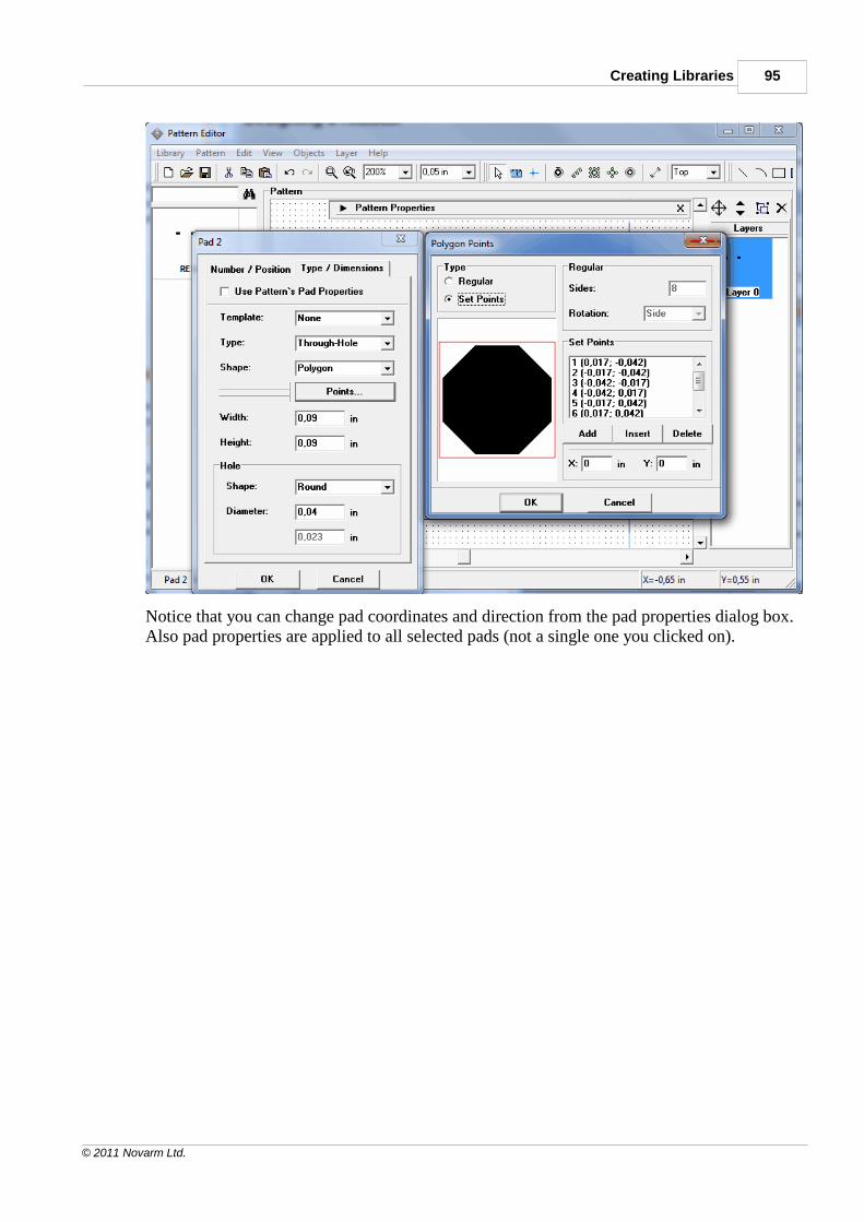
Creating Libraries 95
© 2011 Novarm Ltd.
Notice that you can change pad coordinates and direction from the pad properties dialog box.Also pad properties are applied to all selected pads (not a single one you clicked on).
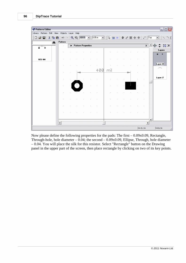
DipTrace Tutorial96
© 2011 Novarm Ltd.
Now please define the following properties for the pads: The first – 0.09x0.09, Rectangle,Through-hole, hole diameter – 0.04; the second – 0.09x0.09, Ellipse, Through, hole diameter– 0.04. You will place the silk for this resistor. Select "Rectangle" button on the Drawingpanel in the upper part of the screen, then place rectangle by clicking on two of its key points.
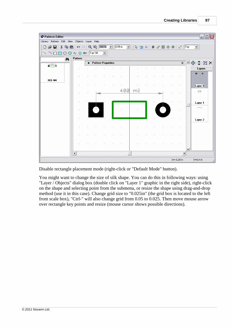
Creating Libraries 97
© 2011 Novarm Ltd.
Disable rectangle placement mode (right-click or "Default Mode" button).
You might want to change the size of silk shape. You can do this in following ways: using"Layer / Objects" dialog box (double click on "Layer 1" graphic in the right side), right-clickon the shape and selecting point from the submenu, or resize the shape using drag-and-dropmethod (use it in this case). Change grid size to "0.025in" (the grid box is located to the leftfrom scale box), "Ctrl-" will also change grid from 0.05 to 0.025. Then move mouse arrowover rectangle key points and resize (mouse cursor shows possible directions).
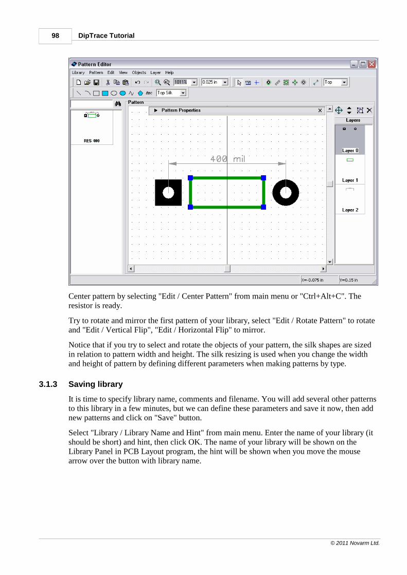
DipTrace Tutorial98
© 2011 Novarm Ltd.
Center pattern by selecting "Edit / Center Pattern" from main menu or "Ctrl+Alt+C". Theresistor is ready.
Try to rotate and mirror the first pattern of your library, select "Edit / Rotate Pattern" to rotateand "Edit / Vertical Flip", "Edit / Horizontal Flip" to mirror.
Notice that if you try to select and rotate the objects of your pattern, the silk shapes are sizedin relation to pattern width and height. The silk resizing is used when you change the widthand height of pattern by defining different parameters when making patterns by type.
3.1.3 Saving library
It is time to specify library name, comments and filename. You will add several other patternsto this library in a few minutes, but we can define these parameters and save it now, then addnew patterns and click on "Save" button.
Select "Library / Library Name and Hint" from main menu. Enter the name of your library (itshould be short) and hint, then click OK. The name of your library will be shown on theLibrary Panel in PCB Layout program, the hint will be shown when you move the mousearrow over the button with library name.
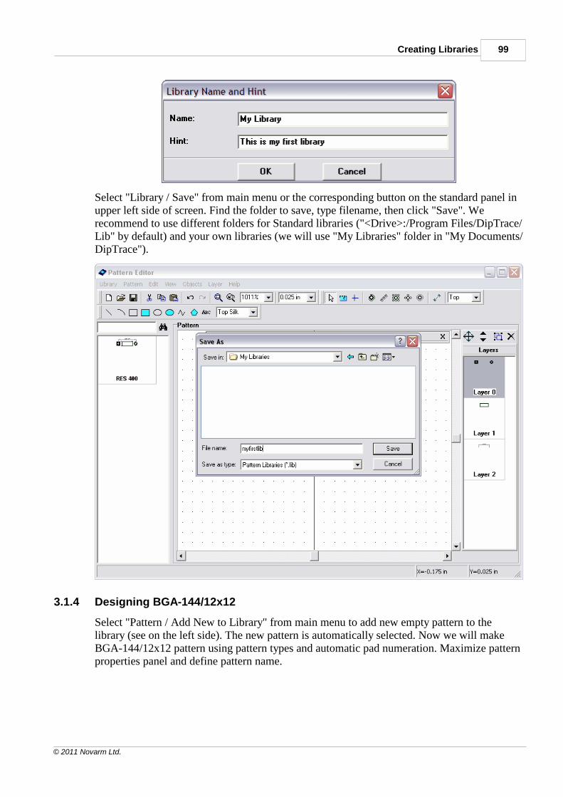
Creating Libraries 99
© 2011 Novarm Ltd.
Select "Library / Save" from main menu or the corresponding button on the standard panel inupper left side of screen. Find the folder to save, type filename, then click "Save". Werecommend to use different folders for Standard libraries ("<Drive>:/Program Files/DipTrace/Lib" by default) and your own libraries (we will use "My Libraries" folder in "My Documents/DipTrace").
3.1.4 Designing BGA-144/12x12
Select "Pattern / Add New to Library" from main menu to add new empty pattern to thelibrary (see on the left side). The new pattern is automatically selected. Now we will makeBGA-144/12x12 pattern using pattern types and automatic pad numeration. Maximize patternproperties panel and define pattern name.
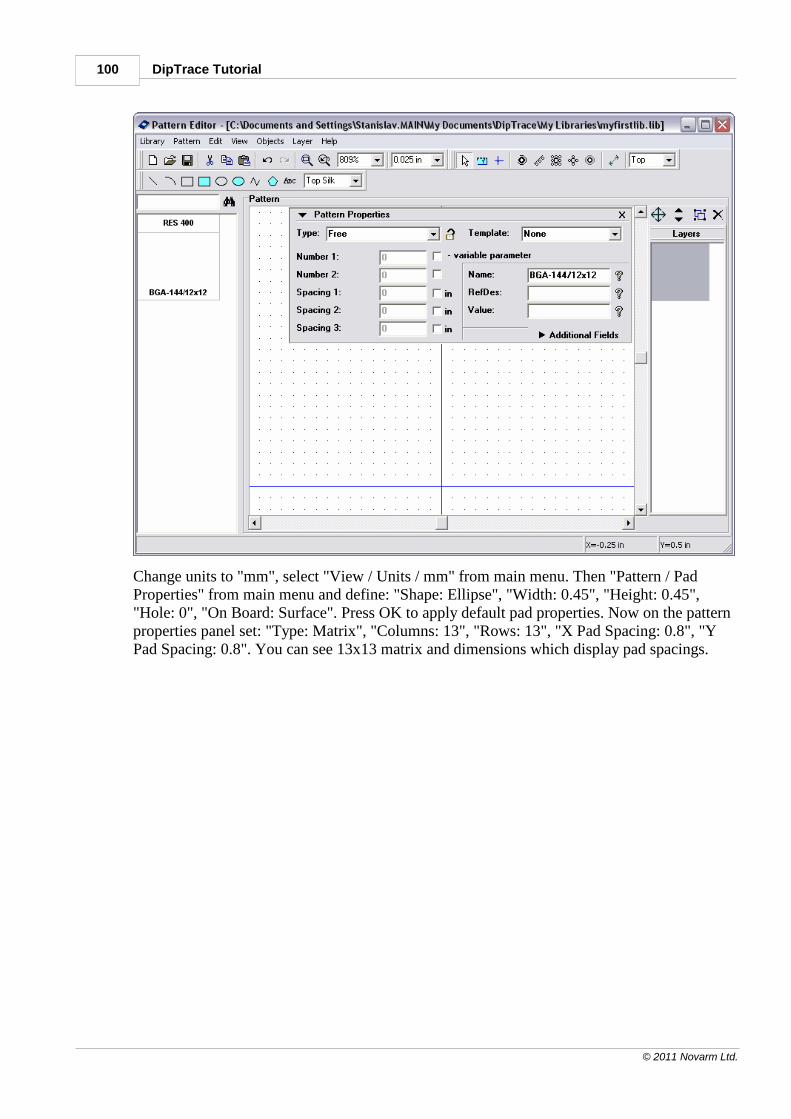
DipTrace Tutorial100
© 2011 Novarm Ltd.
Change units to "mm", select "View / Units / mm" from main menu. Then "Pattern / PadProperties" from main menu and define: "Shape: Ellipse", "Width: 0.45", "Height: 0.45","Hole: 0", "On Board: Surface". Press OK to apply default pad properties. Now on the patternproperties panel set: "Type: Matrix", "Columns: 13", "Rows: 13", "X Pad Spacing: 0.8", "YPad Spacing: 0.8". You can see 13x13 matrix and dimensions which display pad spacings.
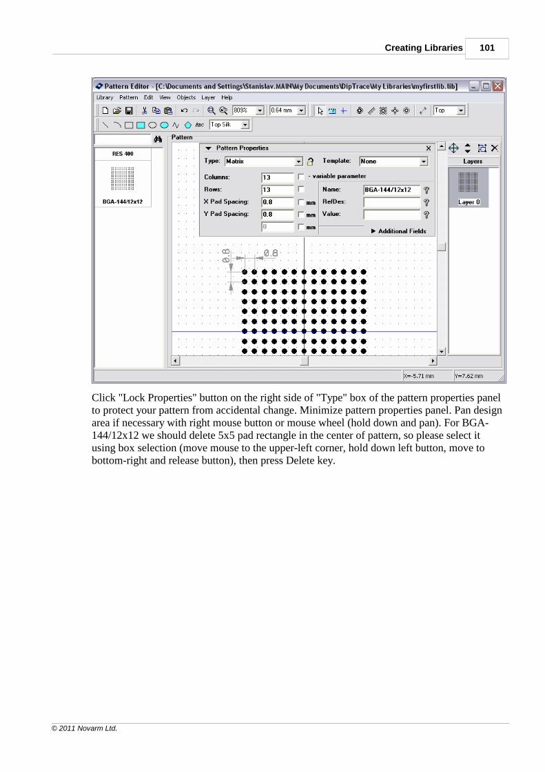
Creating Libraries 101
© 2011 Novarm Ltd.
Click "Lock Properties" button on the right side of "Type" box of the pattern properties panelto protect your pattern from accidental change. Minimize pattern properties panel. Pan designarea if necessary with right mouse button or mouse wheel (hold down and pan). For BGA-144/12x12 we should delete 5x5 pad rectangle in the center of pattern, so please select itusing box selection (move mouse to the upper-left corner, hold down left button, move tobottom-right and release button), then press Delete key.
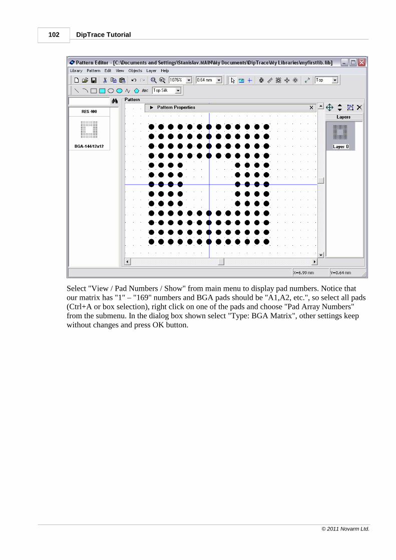
DipTrace Tutorial102
© 2011 Novarm Ltd.
Select "View / Pad Numbers / Show" from main menu to display pad numbers. Notice thatour matrix has "1" – "169" numbers and BGA pads should be "A1,A2, etc.", so select all pads(Ctrl+A or box selection), right click on one of the pads and choose "Pad Array Numbers"from the submenu. In the dialog box shown select "Type: BGA Matrix", other settings keepwithout changes and press OK button.
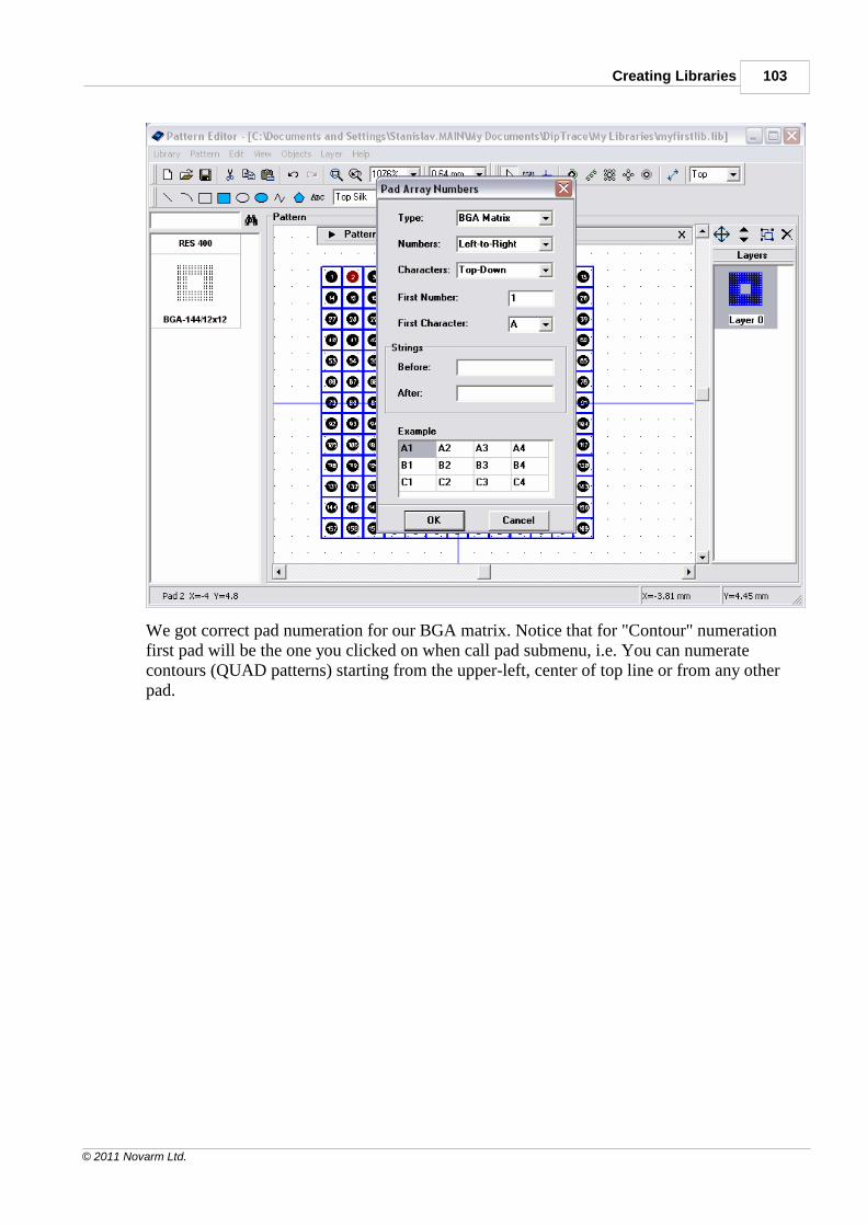
Creating Libraries 103
© 2011 Novarm Ltd.
We got correct pad numeration for our BGA matrix. Notice that for "Contour" numerationfirst pad will be the one you clicked on when call pad submenu, i.e. You can numeratecontours (QUAD patterns) starting from the upper-left, center of top line or from any otherpad.
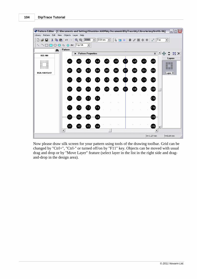
DipTrace Tutorial104
© 2011 Novarm Ltd.
Now please draw silk screen for your pattern using tools of the drawing toolbar. Grid can bechanged by "Ctrl+", "Ctrl-" or turned off/on by "F11" key. Objects can be moved with usualdrag and drop or by "Move Layer" feature (select layer in the list in the right side and drag-and-drop in the design area).
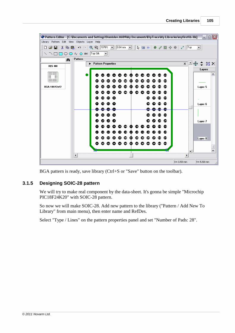
Creating Libraries 105
© 2011 Novarm Ltd.
BGA pattern is ready, save library (Ctrl+S or "Save" button on the toolbar).
3.1.5 Designing SOIC-28 pattern
We will try to make real component by the data-sheet. It's gonna be simple "MicrochipPIC18F24K20" with SOIC-28 pattern.
So now we will make SOIC-28. Add new pattern to the library ("Pattern / Add New ToLibrary" from main menu), then enter name and RefDes.
Select "Type / Lines" on the pattern properties panel and set "Number of Pads: 28".
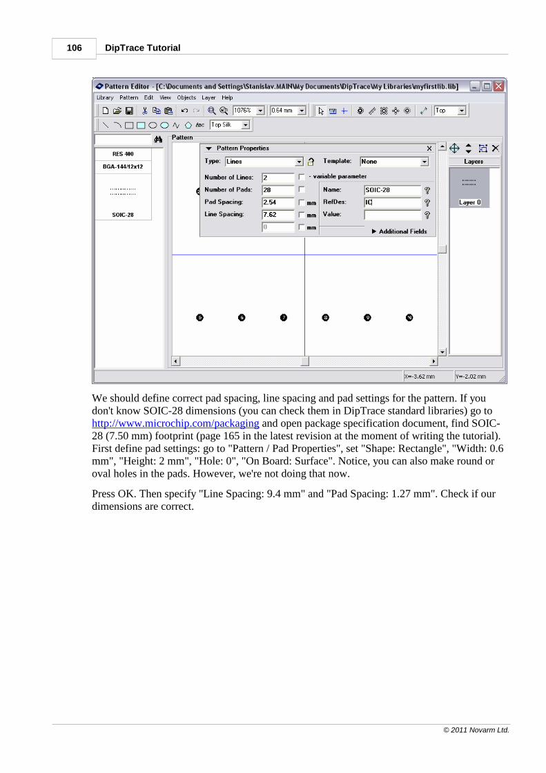
DipTrace Tutorial106
© 2011 Novarm Ltd.
We should define correct pad spacing, line spacing and pad settings for the pattern. If youdon't know SOIC-28 dimensions (you can check them in DipTrace standard libraries) go to http://www.microchip.com/packaging and open package specification document, find SOIC-28 (7.50 mm) footprint (page 165 in the latest revision at the moment of writing the tutorial).First define pad settings: go to "Pattern / Pad Properties", set "Shape: Rectangle", "Width: 0.6mm", "Height: 2 mm", "Hole: 0", "On Board: Surface". Notice, you can also make round oroval holes in the pads. However, we're not doing that now.
Press OK. Then specify "Line Spacing: 9.4 mm" and "Pad Spacing: 1.27 mm". Check if ourdimensions are correct.
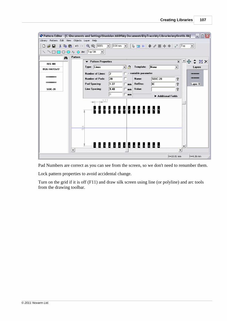
Creating Libraries 107
© 2011 Novarm Ltd.
Pad Numbers are correct as you can see from the screen, so we don't need to renumber them.
Lock pattern properties to avoid accidental change.
Turn on the grid if it is off (F11) and draw silk screen using line (or polyline) and arc toolsfrom the drawing toolbar.
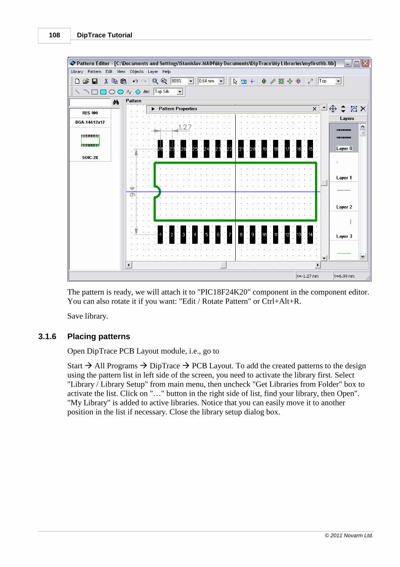
DipTrace Tutorial108
© 2011 Novarm Ltd.
The pattern is ready, we will attach it to "PIC18F24K20" component in the component editor.You can also rotate it if you want: "Edit / Rotate Pattern" or Ctrl+Alt+R.
Save library.
3.1.6 Placing patterns
Open DipTrace PCB Layout module, i.e., go to
Start All Programs DipTrace PCB Layout. To add the created patterns to the designusing the pattern list in left side of the screen, you need to activate the library first. Select"Library / Library Setup" from main menu, then uncheck "Get Libraries from Folder" box toactivate the list. Click on "…" button in the right side of list, find your library, then Open"."My Library" is added to active libraries. Notice that you can easily move it to anotherposition in the list if necessary. Close the library setup dialog box.
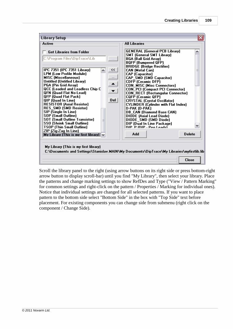
Creating Libraries 109
© 2011 Novarm Ltd.
Scroll the library panel to the right (using arrow buttons on its right side or press bottom-rightarrow button to display scroll-bar) until you find "My Library", then select your library. Placethe patterns and change marking settings to show RefDes and Type ("View / Pattern Marking"for common settings and right-click on the pattern / Properties / Marking for individual ones).Notice that individual settings are changed for all selected patterns. If you want to placepattern to the bottom side select "Bottom Side" in the box with "Top Side" text beforeplacement. For existing components you can change side from submenu (right click on thecomponent / Change Side).
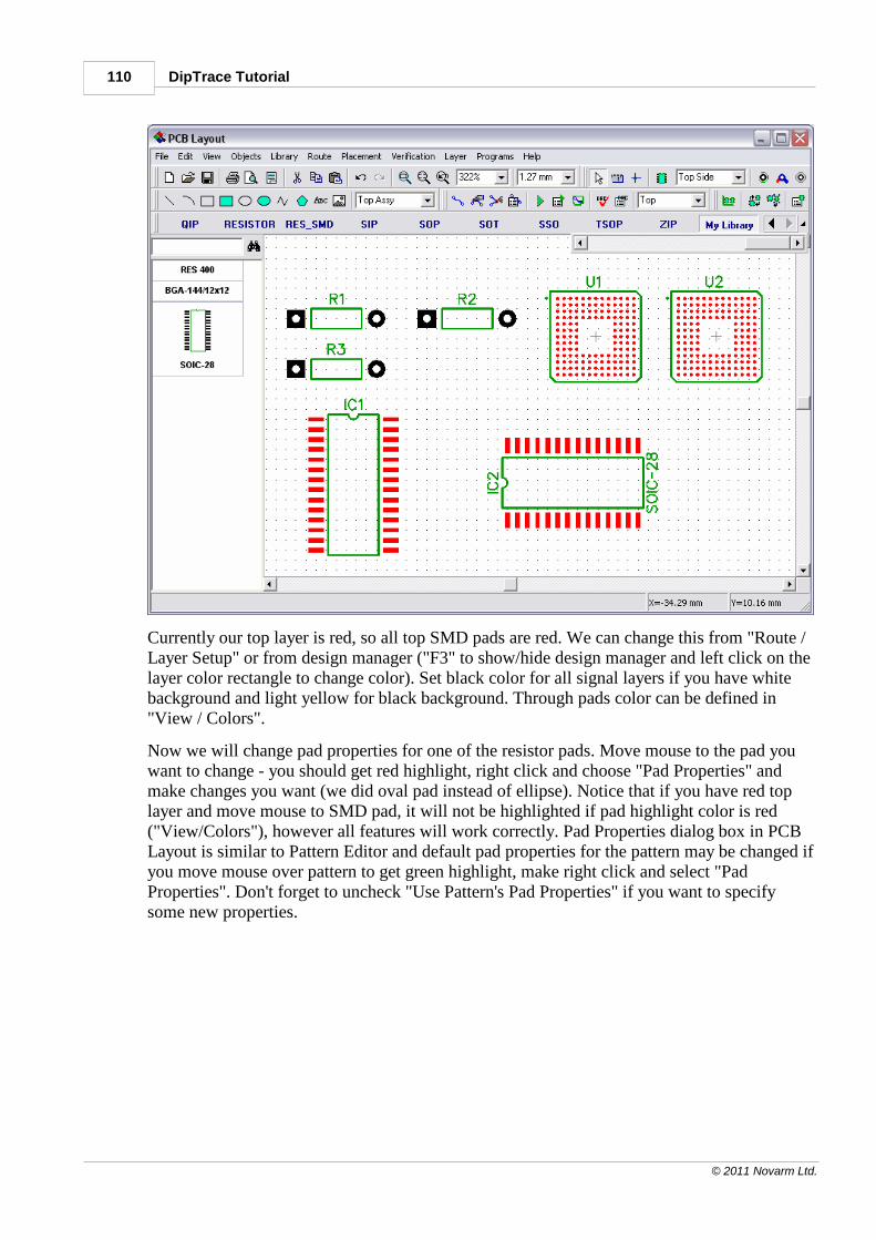
DipTrace Tutorial110
© 2011 Novarm Ltd.
Currently our top layer is red, so all top SMD pads are red. We can change this from "Route /Layer Setup" or from design manager ("F3" to show/hide design manager and left click on thelayer color rectangle to change color). Set black color for all signal layers if you have whitebackground and light yellow for black background. Through pads color can be defined in"View / Colors".
Now we will change pad properties for one of the resistor pads. Move mouse to the pad youwant to change - you should get red highlight, right click and choose "Pad Properties" andmake changes you want (we did oval pad instead of ellipse). Notice that if you have red toplayer and move mouse to SMD pad, it will not be highlighted if pad highlight color is red("View/Colors"), however all features will work correctly. Pad Properties dialog box in PCBLayout is similar to Pattern Editor and default pad properties for the pattern may be changed ifyou move mouse over pattern to get green highlight, make right click and select "PadProperties". Don't forget to uncheck "Use Pattern's Pad Properties" if you want to specifysome new properties.
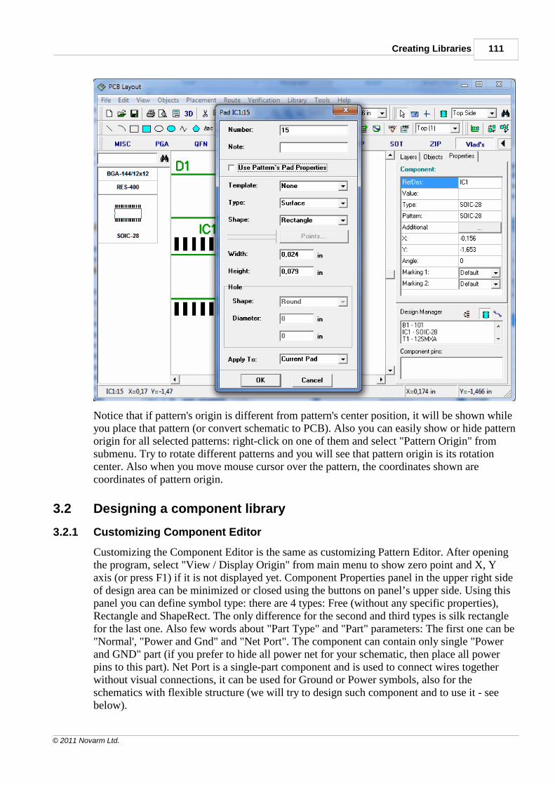
Creating Libraries 111
© 2011 Novarm Ltd.
Notice that if pattern's origin is different from pattern's center position, it will be shown whileyou place that pattern (or convert schematic to PCB). Also you can easily show or hide patternorigin for all selected patterns: right-click on one of them and select "Pattern Origin" fromsubmenu. Try to rotate different patterns and you will see that pattern origin is its rotationcenter. Also when you move mouse cursor over the pattern, the coordinates shown arecoordinates of pattern origin.
3.2 Designing a component library
3.2.1 Customizing Component Editor
Customizing the Component Editor is the same as customizing Pattern Editor. After openingthe program, select "View / Display Origin" from main menu to show zero point and X, Yaxis (or press F1) if it is not displayed yet. Component Properties panel in the upper right sideof design area can be minimized or closed using the buttons on panel’s upper side. Using thispanel you can define symbol type: there are 4 types: Free (without any specific properties),Rectangle and ShapeRect. The only difference for the second and third types is silk rectanglefor the last one. Also few words about "Part Type" and "Part" parameters: The first one can be"Normal', "Power and Gnd" and "Net Port". The component can contain only single "Powerand GND" part (if you prefer to hide all power net for your schematic, then place all powerpins to this part). Net Port is a single-part component and is used to connect wires togetherwithout visual connections, it can be used for Ground or Power symbols, also for theschematics with flexible structure (we will try to design such component and to use it - seebelow).
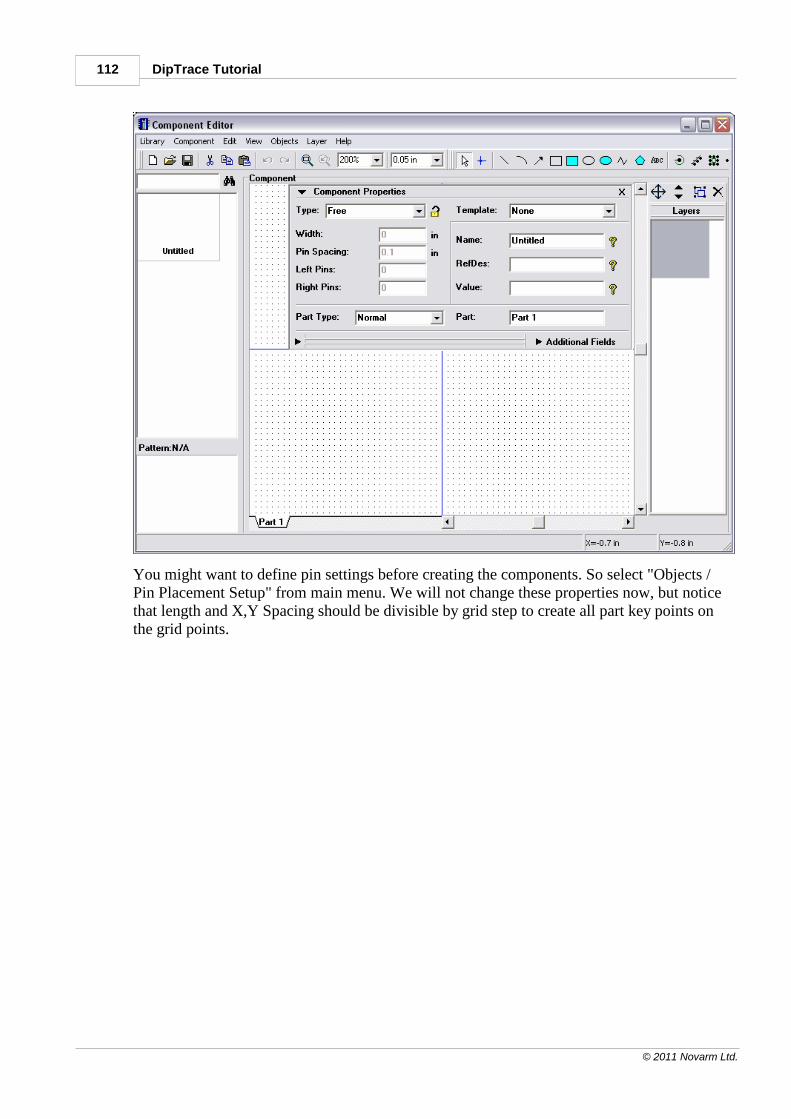
DipTrace Tutorial112
© 2011 Novarm Ltd.
You might want to define pin settings before creating the components. So select "Objects /Pin Placement Setup" from main menu. We will not change these properties now, but noticethat length and X,Y Spacing should be divisible by grid step to create all part key points onthe grid points.
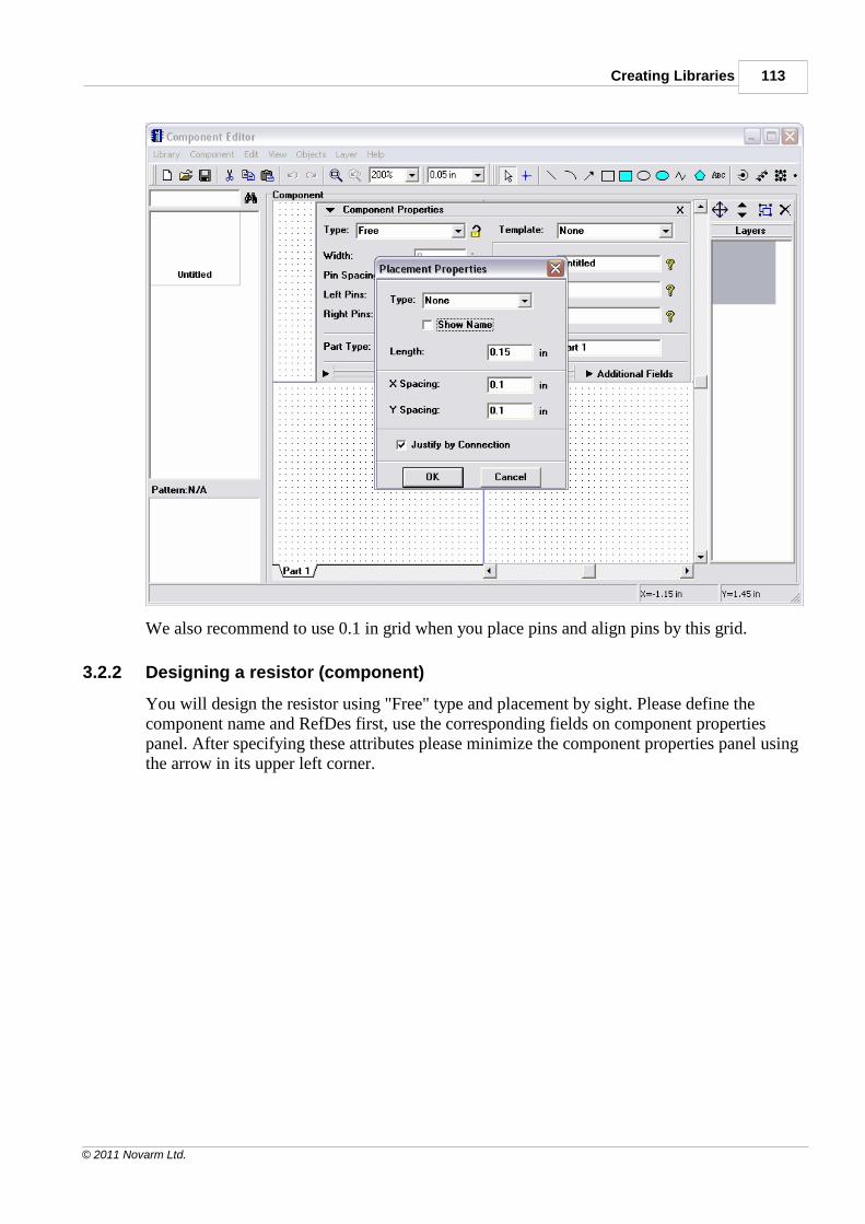
Creating Libraries 113
© 2011 Novarm Ltd.
We also recommend to use 0.1 in grid when you place pins and align pins by this grid.
3.2.2 Designing a resistor (component)
You will design the resistor using "Free" type and placement by sight. Please define thecomponent name and RefDes first, use the corresponding fields on component propertiespanel. After specifying these attributes please minimize the component properties panel usingthe arrow in its upper left corner.

DipTrace Tutorial114
© 2011 Novarm Ltd.
Select "Place Pin" tool in the upper right side of the screen, then move mouse arrow to designarea and place two pins using left-click. Rotate one pin by 180 degrees: select it and press"Ctrl+R" twice. Select the rectangle tool and place graphics for the resistor. Pins should beplaced by 0.1 grid and rectangle by 0.05 grid (Ctrl+, Ctrl- to change grid on the fly).
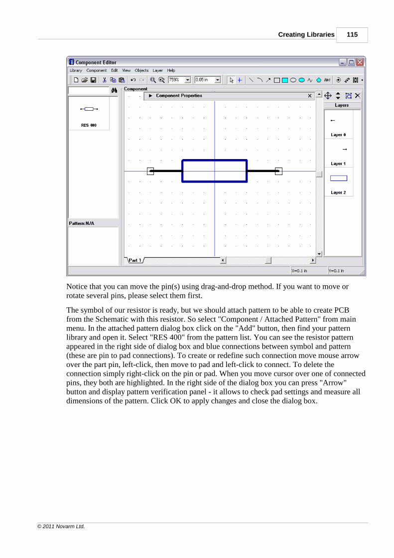
Creating Libraries 115
© 2011 Novarm Ltd.
Notice that you can move the pin(s) using drag-and-drop method. If you want to move orrotate several pins, please select them first.
The symbol of our resistor is ready, but we should attach pattern to be able to create PCBfrom the Schematic with this resistor. So select "Component / Attached Pattern" from mainmenu. In the attached pattern dialog box click on the "Add" button, then find your patternlibrary and open it. Select "RES 400" from the pattern list. You can see the resistor patternappeared in the right side of dialog box and blue connections between symbol and pattern(these are pin to pad connections). To create or redefine such connection move mouse arrowover the part pin, left-click, then move to pad and left-click to connect. To delete theconnection simply right-click on the pin or pad. When you move cursor over one of connectedpins, they both are highlighted. In the right side of the dialog box you can press "Arrow"button and display pattern verification panel - it allows to check pad settings and measure alldimensions of the pattern. Click OK to apply changes and close the dialog box.
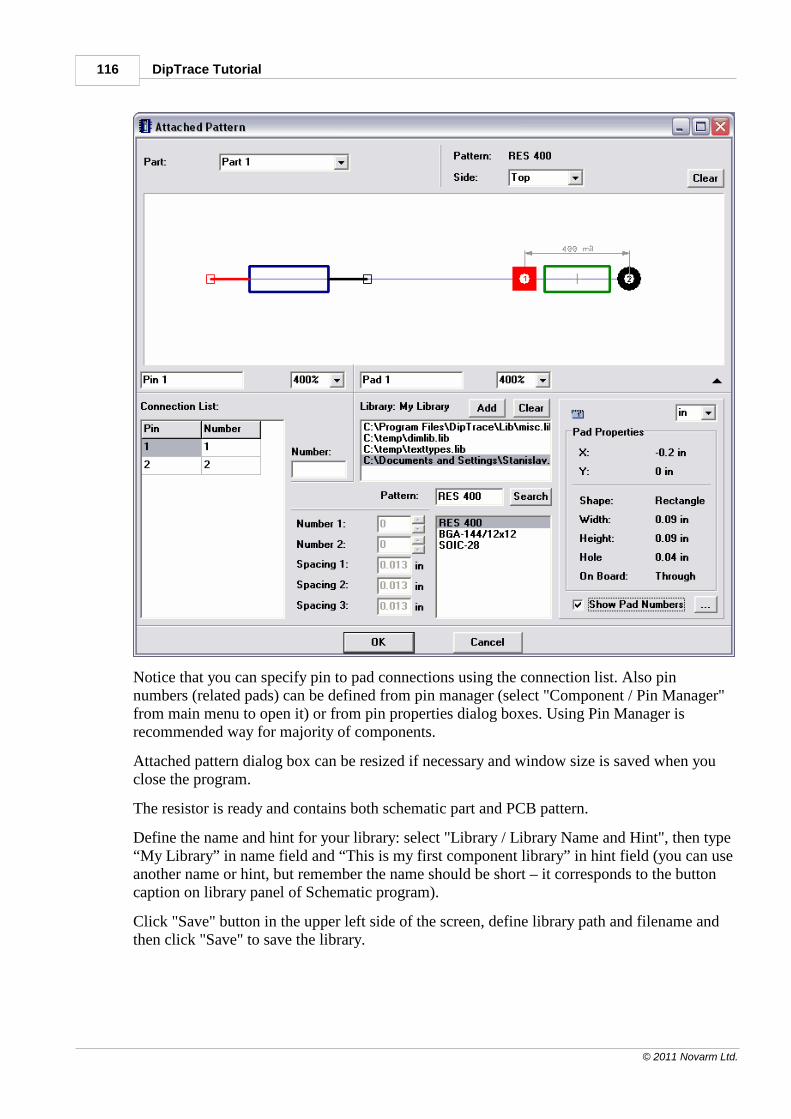
DipTrace Tutorial116
© 2011 Novarm Ltd.
Notice that you can specify pin to pad connections using the connection list. Also pinnumbers (related pads) can be defined from pin manager (select "Component / Pin Manager"from main menu to open it) or from pin properties dialog boxes. Using Pin Manager isrecommended way for majority of components.
Attached pattern dialog box can be resized if necessary and window size is saved when youclose the program.
The resistor is ready and contains both schematic part and PCB pattern.
Define the name and hint for your library: select "Library / Library Name and Hint", then type“My Library” in name field and “This is my first component library” in hint field (you can useanother name or hint, but remember the name should be short – it corresponds to the buttoncaption on library panel of Schematic program).
Click "Save" button in the upper left side of the screen, define library path and filename andthen click "Save" to save the library.
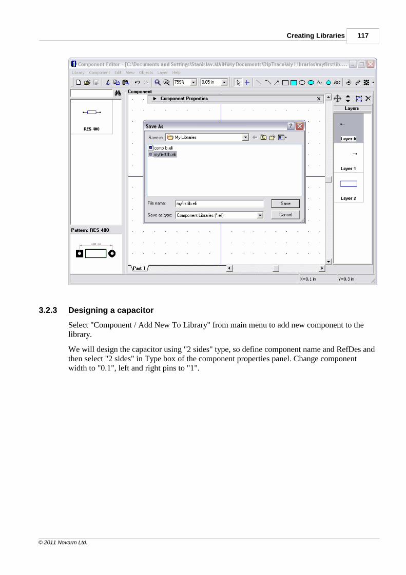
Creating Libraries 117
© 2011 Novarm Ltd.
3.2.3 Designing a capacitor
Select "Component / Add New To Library" from main menu to add new component to thelibrary.
We will design the capacitor using "2 sides" type, so define component name and RefDes andthen select "2 sides" in Type box of the component properties panel. Change componentwidth to "0.1", left and right pins to "1".
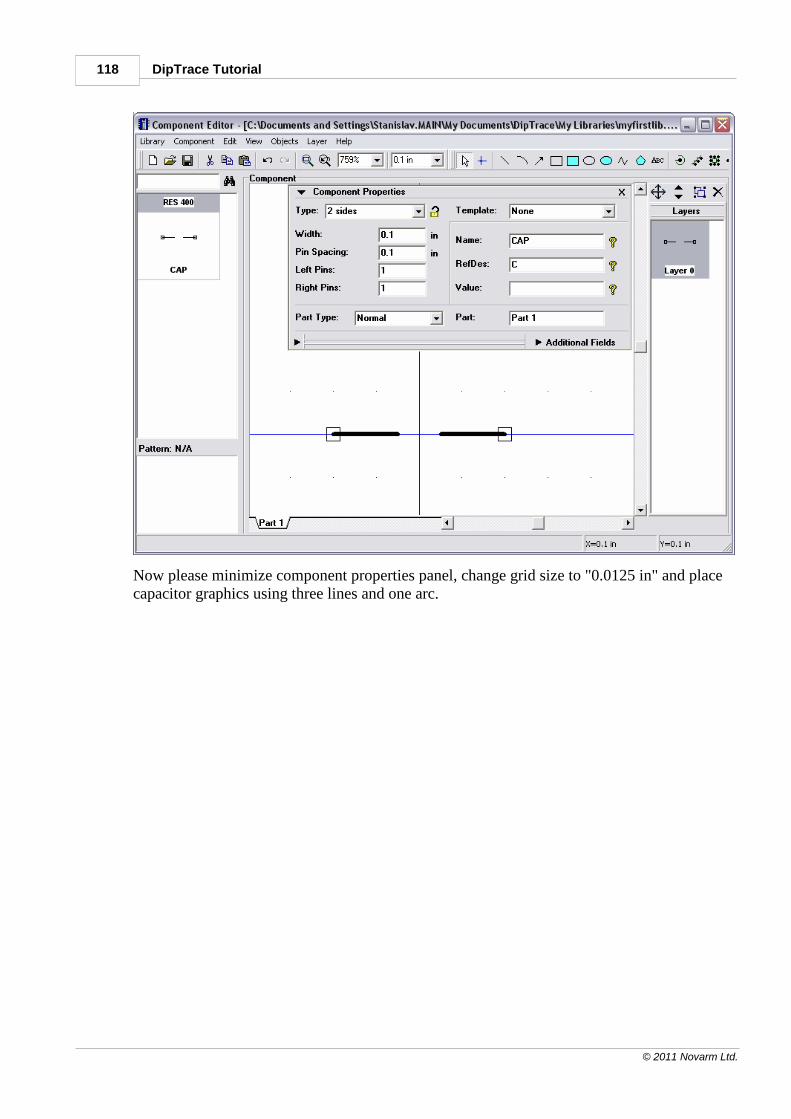
DipTrace Tutorial118
© 2011 Novarm Ltd.
Now please minimize component properties panel, change grid size to "0.0125 in" and placecapacitor graphics using three lines and one arc.
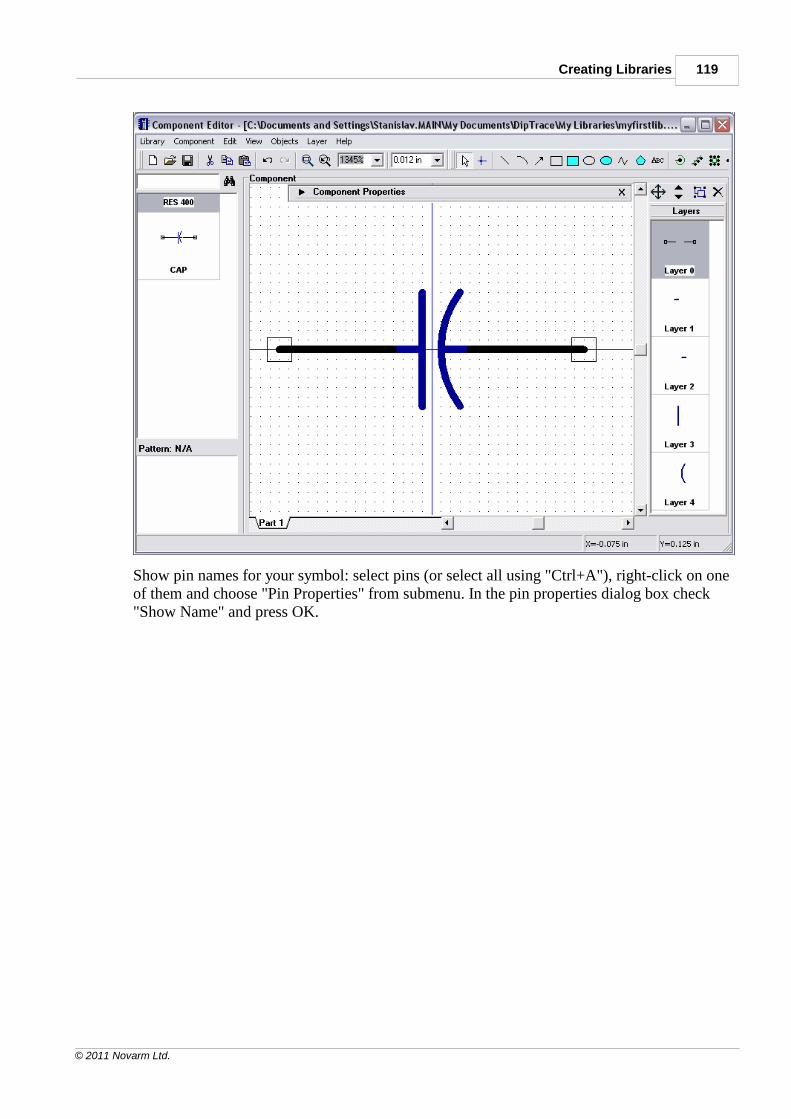
Creating Libraries 119
© 2011 Novarm Ltd.
Show pin names for your symbol: select pins (or select all using "Ctrl+A"), right-click on oneof them and choose "Pin Properties" from submenu. In the pin properties dialog box check"Show Name" and press OK.
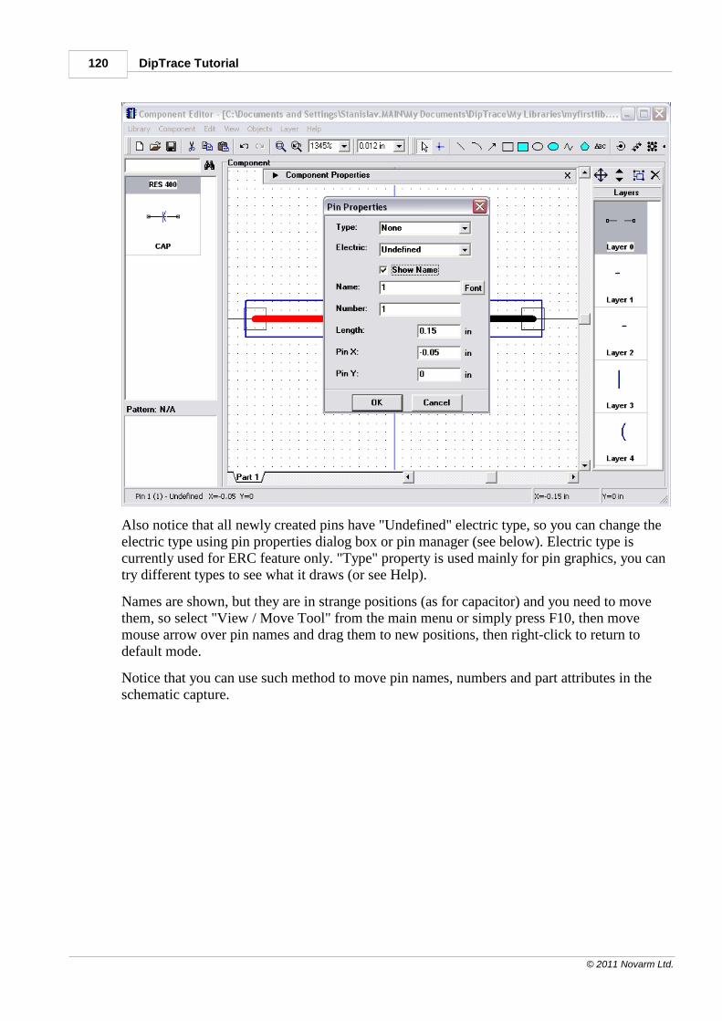
DipTrace Tutorial120
© 2011 Novarm Ltd.
Also notice that all newly created pins have "Undefined" electric type, so you can change theelectric type using pin properties dialog box or pin manager (see below). Electric type iscurrently used for ERC feature only. "Type" property is used mainly for pin graphics, you cantry different types to see what it draws (or see Help).
Names are shown, but they are in strange positions (as for capacitor) and you need to movethem, so select "View / Move Tool" from the main menu or simply press F10, then movemouse arrow over pin names and drag them to new positions, then right-click to return todefault mode.
Notice that you can use such method to move pin names, numbers and part attributes in theschematic capture.
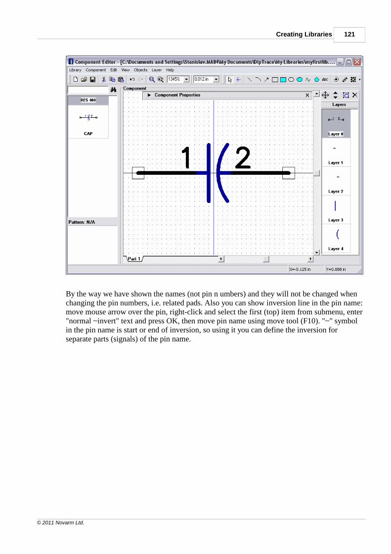
Creating Libraries 121
© 2011 Novarm Ltd.
By the way we have shown the names (not pin n umbers) and they will not be changed whenchanging the pin numbers, i.e. related pads. Also you can show inversion line in the pin name:move mouse arrow over the pin, right-click and select the first (top) item from submenu, enter"normal ~invert" text and press OK, then move pin name using move tool (F10). "~" symbolin the pin name is start or end of inversion, so using it you can define the inversion forseparate parts (signals) of the pin name.
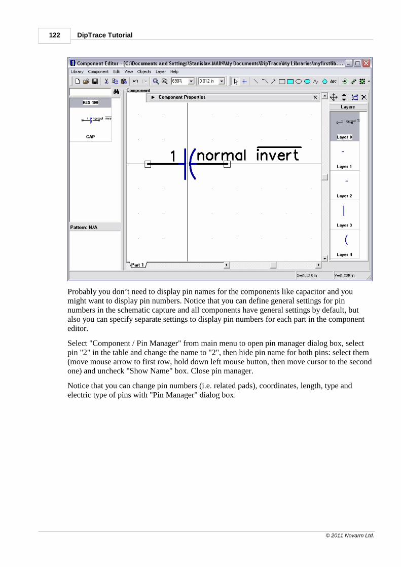
DipTrace Tutorial122
© 2011 Novarm Ltd.
Probably you don’t need to display pin names for the components like capacitor and youmight want to display pin numbers. Notice that you can define general settings for pinnumbers in the schematic capture and all components have general settings by default, butalso you can specify separate settings to display pin numbers for each part in the componenteditor.
Select "Component / Pin Manager" from main menu to open pin manager dialog box, selectpin "2" in the table and change the name to "2", then hide pin name for both pins: select them(move mouse arrow to first row, hold down left mouse button, then move cursor to the secondone) and uncheck "Show Name" box. Close pin manager.
Notice that you can change pin numbers (i.e. related pads), coordinates, length, type andelectric type of pins with "Pin Manager" dialog box.
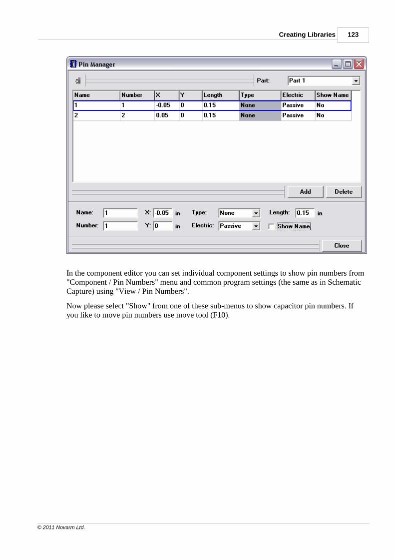
Creating Libraries 123
© 2011 Novarm Ltd.
In the component editor you can set individual component settings to show pin numbers from"Component / Pin Numbers" menu and common program settings (the same as in SchematicCapture) using "View / Pin Numbers".
Now please select "Show" from one of these sub-menus to show capacitor pin numbers. Ifyou like to move pin numbers use move tool (F10).
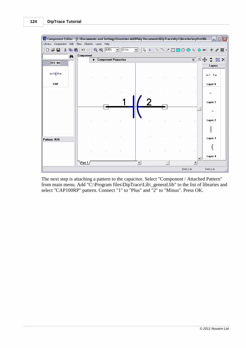
DipTrace Tutorial124
© 2011 Novarm Ltd.
The next step is attaching a pattern to the capacitor. Select "Component / Attached Pattern"from main menu. Add "C:\Program files\DipTrace\Lib\_general.lib" to the list of libraries andselect "CAP100RP" pattern. Connect "1" to "Plus" and "2" to "Minus". Press OK.
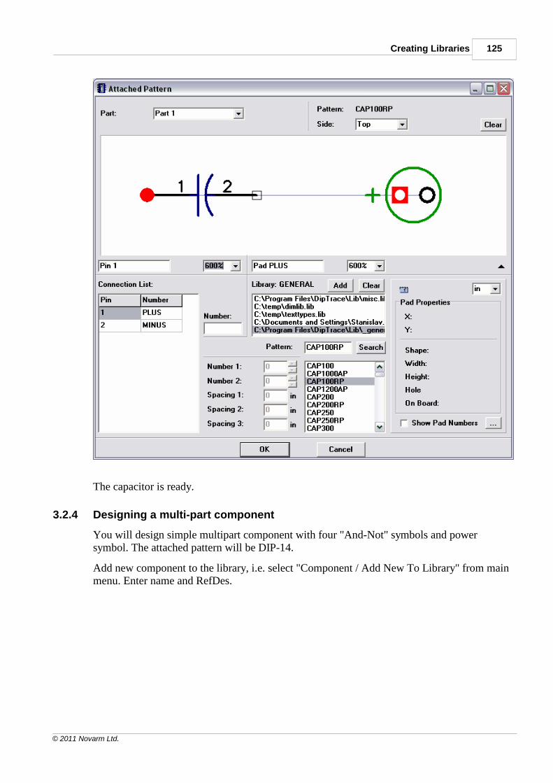
Creating Libraries 125
© 2011 Novarm Ltd.
The capacitor is ready.
3.2.4 Designing a multi-part component
You will design simple multipart component with four "And-Not" symbols and powersymbol. The attached pattern will be DIP-14.
Add new component to the library, i.e. select "Component / Add New To Library" from mainmenu. Enter name and RefDes.
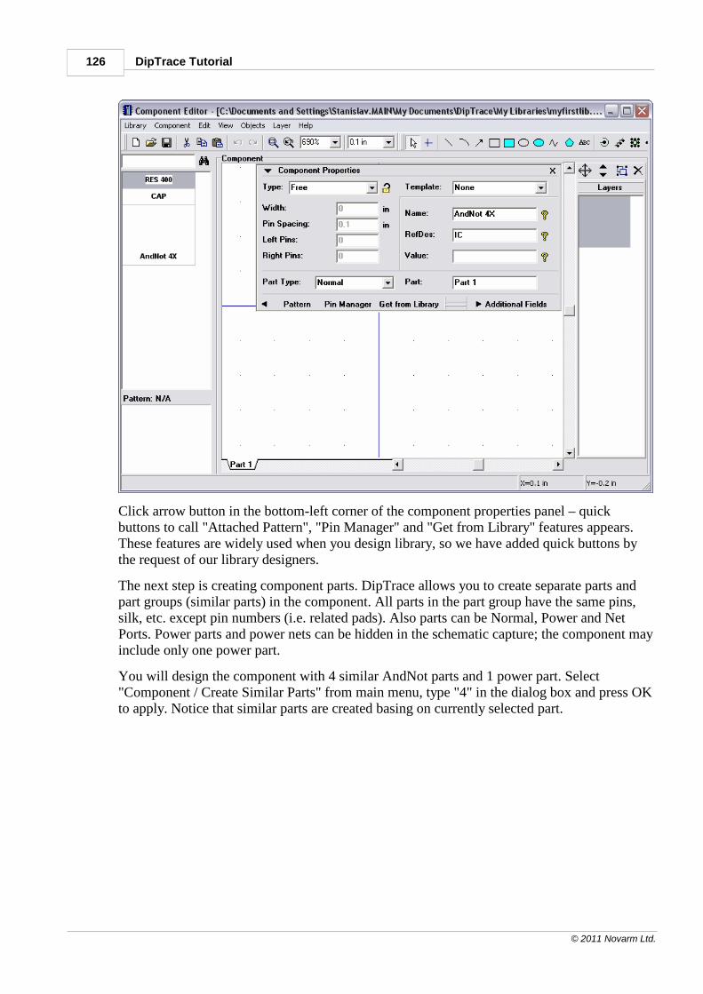
DipTrace Tutorial126
© 2011 Novarm Ltd.
Click arrow button in the bottom-left corner of the component properties panel – quickbuttons to call "Attached Pattern", "Pin Manager" and "Get from Library" features appears.These features are widely used when you design library, so we have added quick buttons bythe request of our library designers.
The next step is creating component parts. DipTrace allows you to create separate parts andpart groups (similar parts) in the component. All parts in the part group have the same pins,silk, etc. except pin numbers (i.e. related pads). Also parts can be Normal, Power and NetPorts. Power parts and power nets can be hidden in the schematic capture; the component mayinclude only one power part.
You will design the component with 4 similar AndNot parts and 1 power part. Select"Component / Create Similar Parts" from main menu, type "4" in the dialog box and press OKto apply. Notice that similar parts are created basing on currently selected part.
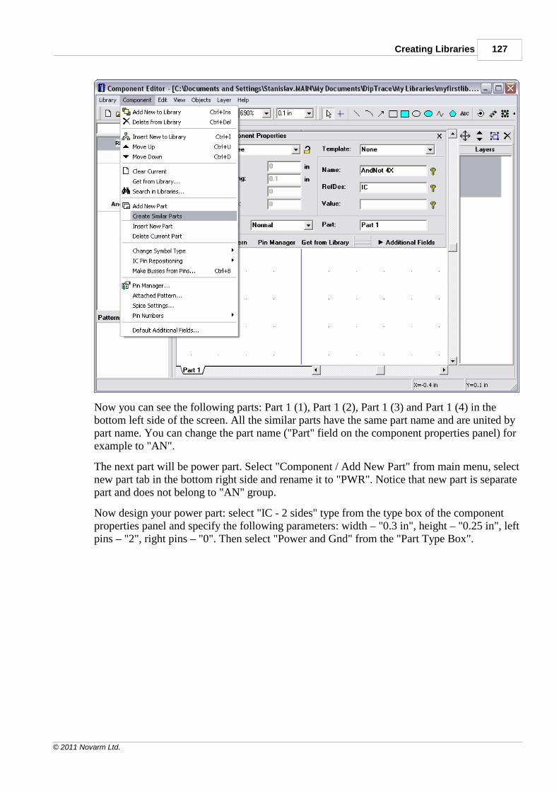
Creating Libraries 127
© 2011 Novarm Ltd.
Now you can see the following parts: Part 1 (1), Part 1 (2), Part 1 (3) and Part 1 (4) in thebottom left side of the screen. All the similar parts have the same part name and are united bypart name. You can change the part name ("Part" field on the component properties panel) forexample to "AN".
The next part will be power part. Select "Component / Add New Part" from main menu, selectnew part tab in the bottom right side and rename it to "PWR". Notice that new part is separatepart and does not belong to "AN" group.
Now design your power part: select "IC - 2 sides" type from the type box of the componentproperties panel and specify the following parameters: width – "0.3 in", height – "0.25 in", leftpins – "2", right pins – "0". Then select "Power and Gnd" from the "Part Type Box".
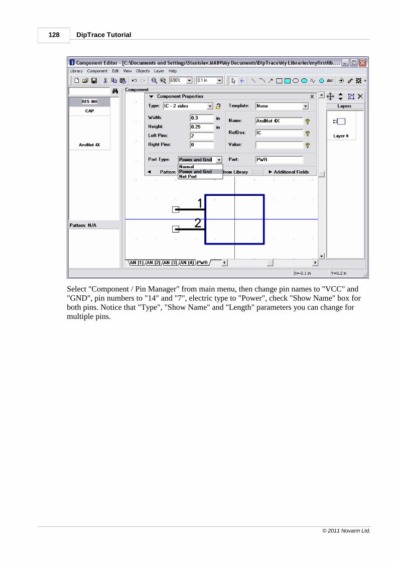
DipTrace Tutorial128
© 2011 Novarm Ltd.
Select "Component / Pin Manager" from main menu, then change pin names to "VCC" and"GND", pin numbers to "14" and "7", electric type to "Power", check "Show Name" box forboth pins. Notice that "Type", "Show Name" and "Length" parameters you can change formultiple pins.
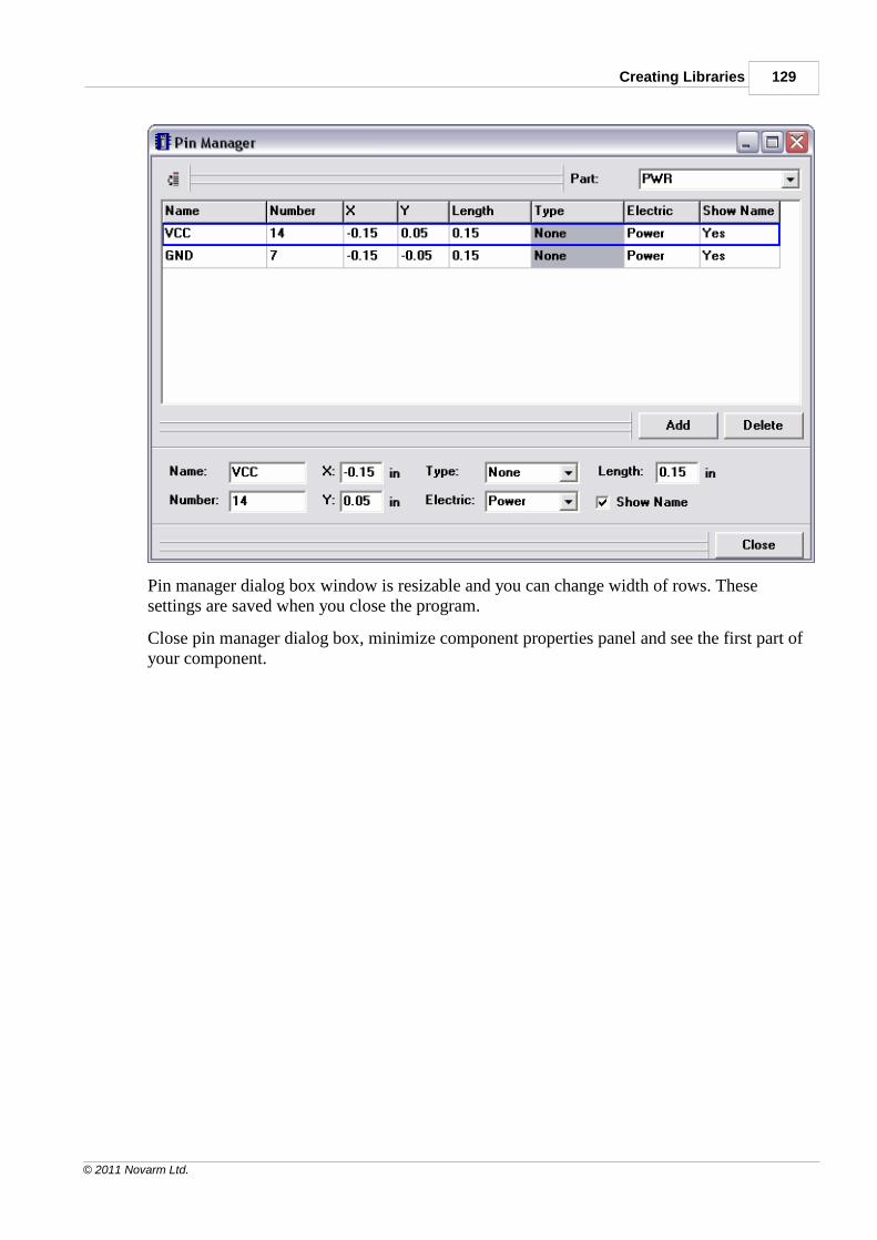
Creating Libraries 129
© 2011 Novarm Ltd.
Pin manager dialog box window is resizable and you can change width of rows. Thesesettings are saved when you close the program.
Close pin manager dialog box, minimize component properties panel and see the first part ofyour component.
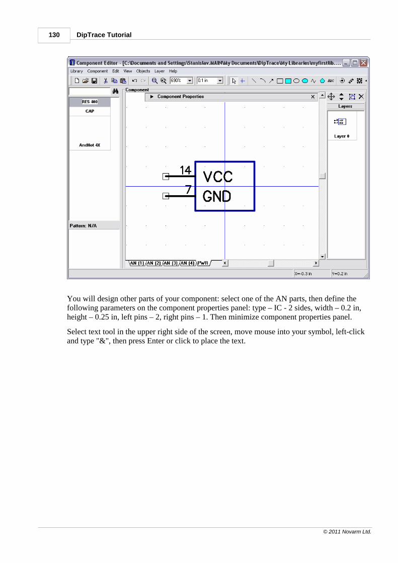
DipTrace Tutorial130
© 2011 Novarm Ltd.
You will design other parts of your component: select one of the AN parts, then define thefollowing parameters on the component properties panel: type – IC - 2 sides, width – 0.2 in,height – 0.25 in, left pins – 2, right pins – 1. Then minimize component properties panel.
Select text tool in the upper right side of the screen, move mouse into your symbol, left-clickand type "&", then press Enter or click to place the text.
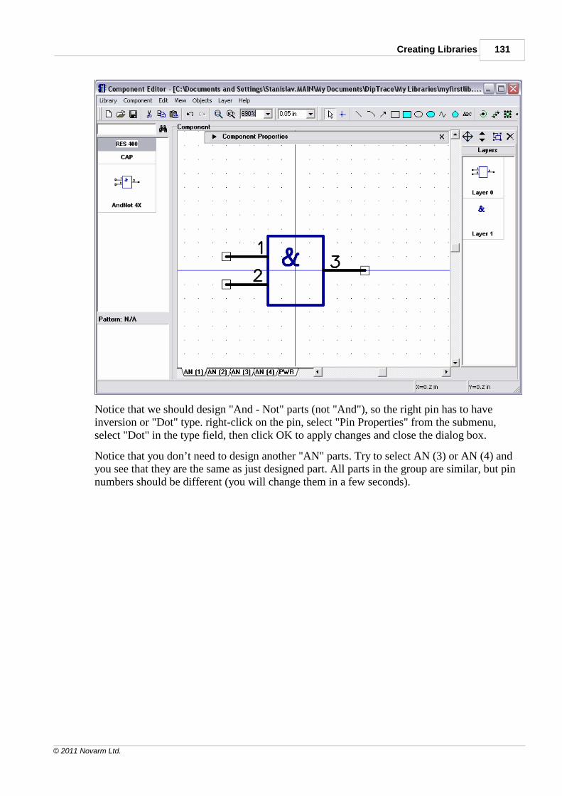
Creating Libraries 131
© 2011 Novarm Ltd.
Notice that we should design "And - Not" parts (not "And"), so the right pin has to haveinversion or "Dot" type. right-click on the pin, select "Pin Properties" from the submenu,select "Dot" in the type field, then click OK to apply changes and close the dialog box.
Notice that you don’t need to design another "AN" parts. Try to select AN (3) or AN (4) andyou see that they are the same as just designed part. All parts in the group are similar, but pinnumbers should be different (you will change them in a few seconds).
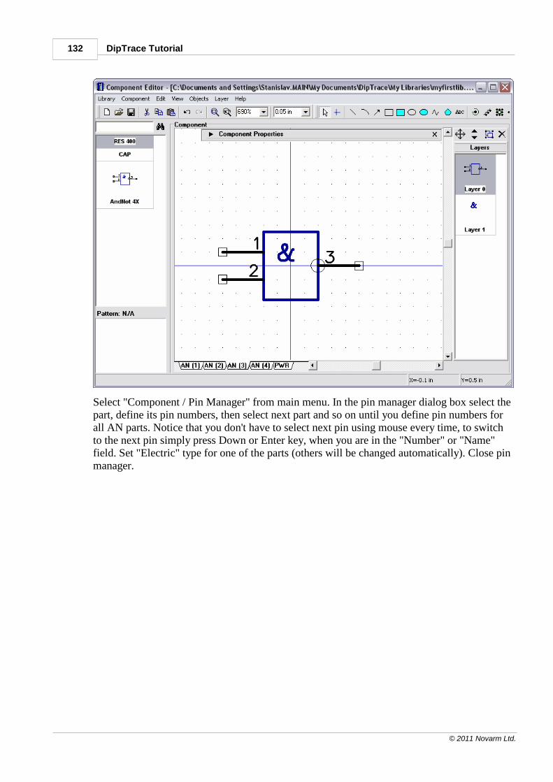
DipTrace Tutorial132
© 2011 Novarm Ltd.
Select "Component / Pin Manager" from main menu. In the pin manager dialog box select thepart, define its pin numbers, then select next part and so on until you define pin numbers forall AN parts. Notice that you don't have to select next pin using mouse every time, to switchto the next pin simply press Down or Enter key, when you are in the "Number" or "Name"field. Set "Electric" type for one of the parts (others will be changed automatically). Close pinmanager.
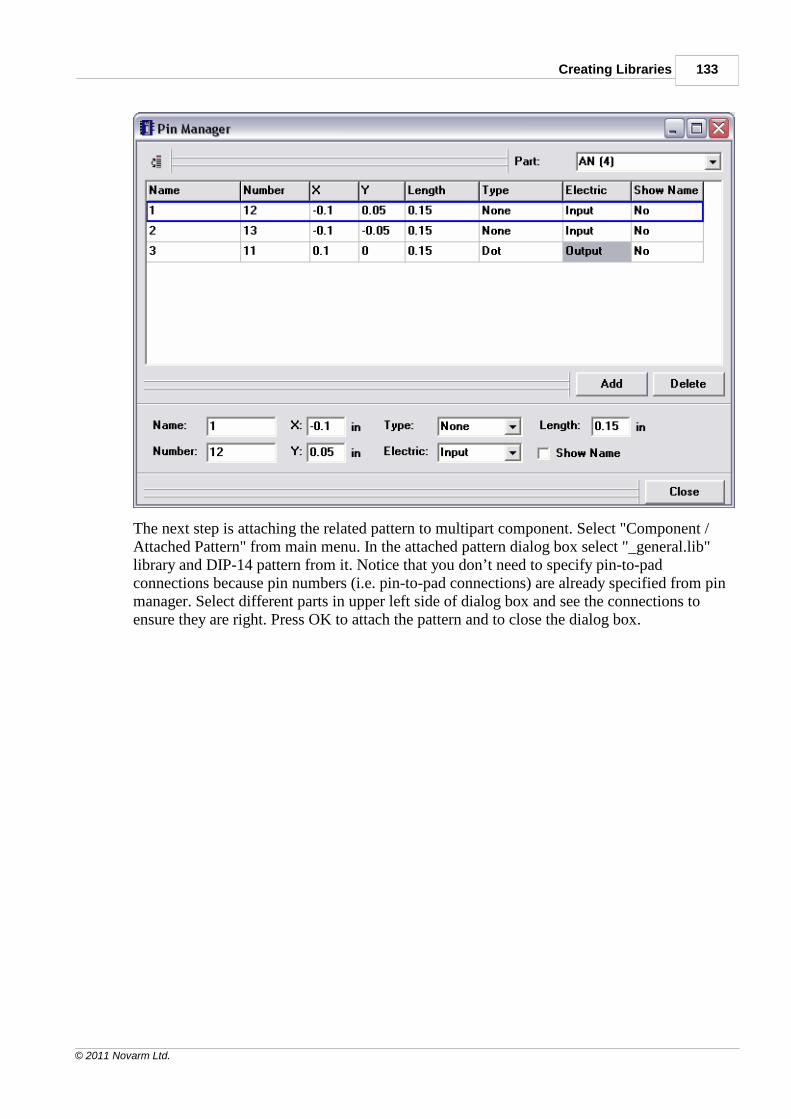
Creating Libraries 133
© 2011 Novarm Ltd.
The next step is attaching the related pattern to multipart component. Select "Component /Attached Pattern" from main menu. In the attached pattern dialog box select "_general.lib"library and DIP-14 pattern from it. Notice that you don’t need to specify pin-to-padconnections because pin numbers (i.e. pin-to-pad connections) are already specified from pinmanager. Select different parts in upper left side of dialog box and see the connections toensure they are right. Press OK to attach the pattern and to close the dialog box.
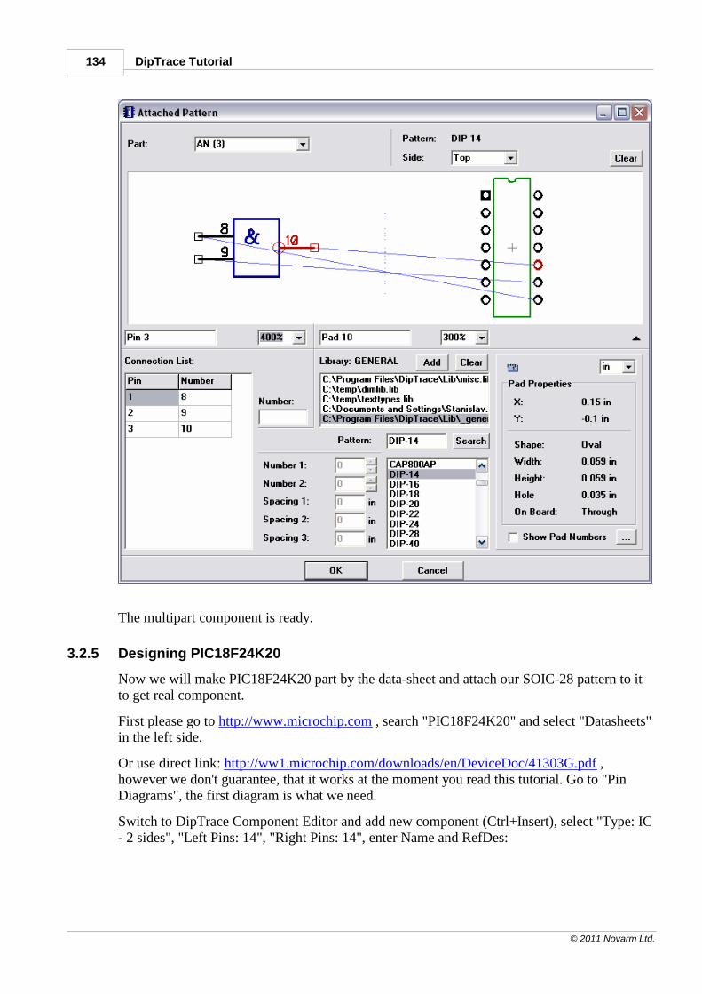
DipTrace Tutorial134
© 2011 Novarm Ltd.
The multipart component is ready.
3.2.5 Designing PIC18F24K20
Now we will make PIC18F24K20 part by the data-sheet and attach our SOIC-28 pattern to itto get real component.
First please go to http://www.microchip.com , search "PIC18F24K20" and select "Datasheets"in the left side.
Or use direct link: http://ww1.microchip.com/downloads/en/DeviceDoc/41303G.pdf ,however we don't guarantee, that it works at the moment you read this tutorial. Go to "PinDiagrams", the first diagram is what we need.
Switch to DipTrace Component Editor and add new component (Ctrl+Insert), select "Type: IC- 2 sides", "Left Pins: 14", "Right Pins: 14", enter Name and RefDes:
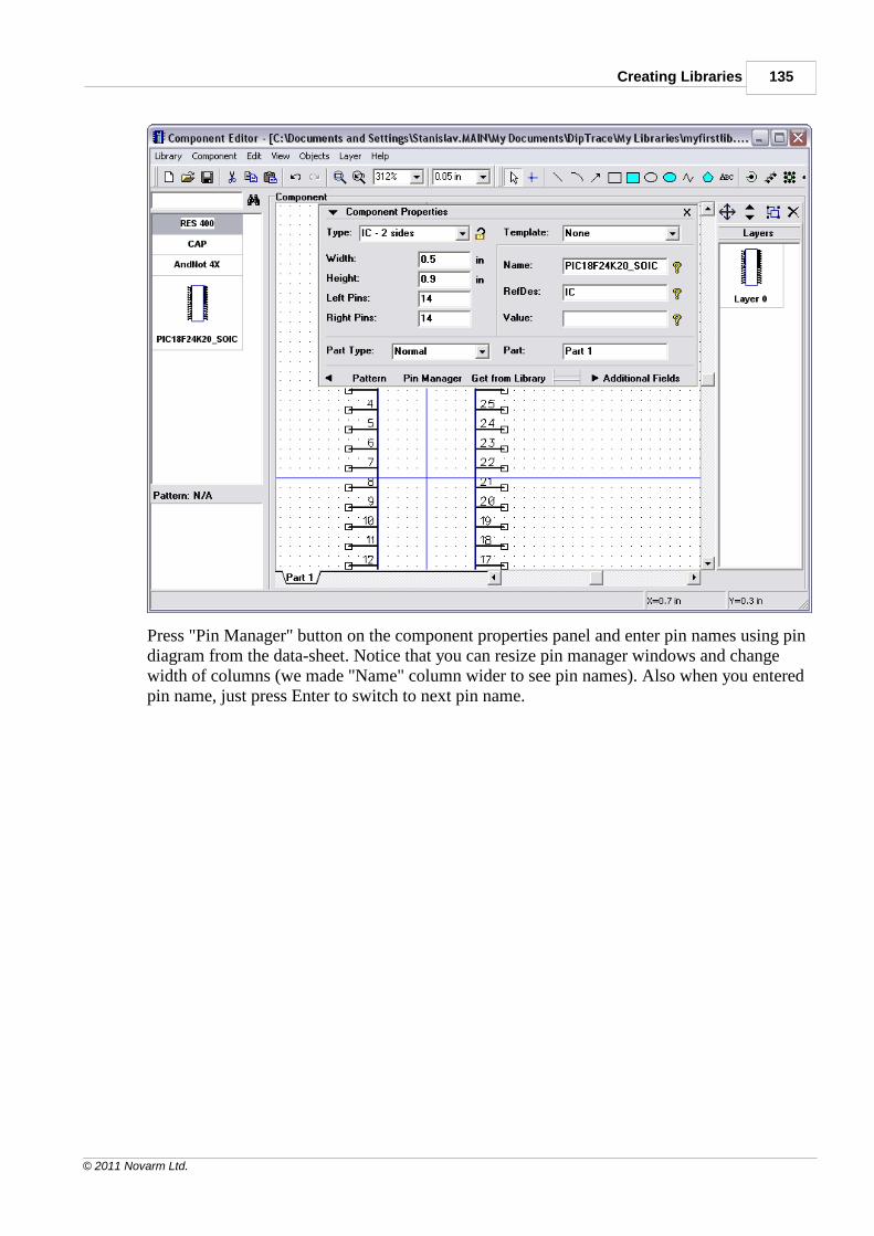
Creating Libraries 135
© 2011 Novarm Ltd.
Press "Pin Manager" button on the component properties panel and enter pin names using pindiagram from the data-sheet. Notice that you can resize pin manager windows and changewidth of columns (we made "Name" column wider to see pin names). Also when you enteredpin name, just press Enter to switch to next pin name.
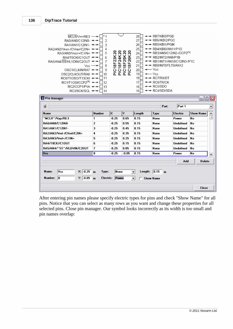
DipTrace Tutorial136
© 2011 Novarm Ltd.
After entering pin names please specify electric types for pins and check "Show Name" for allpins. Notice that you can select as many rows as you want and change these properties for allselected pins. Close pin manager. Our symbol looks incorrectly as its width is too small andpin names overlap:
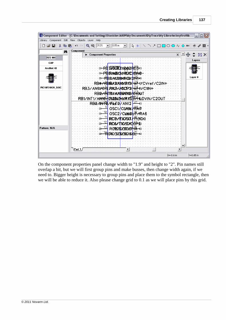
Creating Libraries 137
© 2011 Novarm Ltd.
On the component properties panel change width to "1.9" and height to "2". Pin names stilloverlap a bit, but we will first group pins and make busses, then change width again, if weneed to. Bigger height is necessary to group pins and place them to the symbol rectangle, thenwe will be able to reduce it. Also please change grid to 0.1 as we will place pins by this grid.
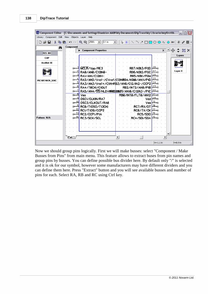
DipTrace Tutorial138
© 2011 Novarm Ltd.
Now we should group pins logically. First we will make busses: select "Component / MakeBusses from Pins" from main menu. This feature allows to extract buses from pin names andgroup pins by busses. You can define possible bus divider here. By default only "/" is selectedand it is ok for our symbol, however some manufacturers may have different dividers and youcan define them here. Press "Extract" button and you will see available busses and number ofpins for each. Select RA, RB and RC using Ctrl key.
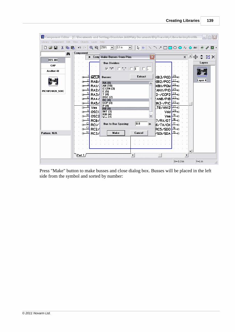
Creating Libraries 139
© 2011 Novarm Ltd.
Press "Make" button to make busses and close dialog box. Busses will be placed in the leftside from the symbol and sorted by number:
DipTrace Tutorial140
© 2011 Novarm Ltd.
Notice that you can also define "Bus-to-Bus Spacing" before making busses.
Now please select all pins that are not in busses (4 pins are still on the symbol as you can see),use "Ctrl" and box selection for multiple select. Right click on one of those pins and "Snap toGrid", then move pins to the bottom to let we place busses first.
Creating Libraries 141
© 2011 Novarm Ltd.
Place busses to the rectangle. Use box selection to select bus, then drag it. Shift+R can beused to rotate bus and "Shift+F" to flip pins in it, these commands can be also selected frompin submenu (right click on one of bus pins). Then move pins from the bottom to therectangle (R can be used to rotate selected object/pin). We got the following symbol, but youcan do that a bit differently:
DipTrace Tutorial142
© 2011 Novarm Ltd.
Also sometimes you need to place pins by electric type, to make this task easier, you canchange pin colors by electric type – see "View / Pin Colors by EType".
Symbol width is correct as you can see, however we can reduce symbol height a bit, sochange height to "1.8" on the component properties panel. Please do not touch number of pinsas this may destroy you symbol (then you can use "Undo" though).
Creating Libraries 143
© 2011 Novarm Ltd.
Lock symbol type on the component properties panel (lock button is located on the right sidefrom Type field) to protect it from accidental change.
Final step is attaching SOIC-28 pattern to our component, so press "Pattern" button on thecomponent properties button and select you "SOIC-28" pattern in Attached Pattern dialogbox. All pin names and pin numbers are already there, so you don't need to change anything.Just press OK.
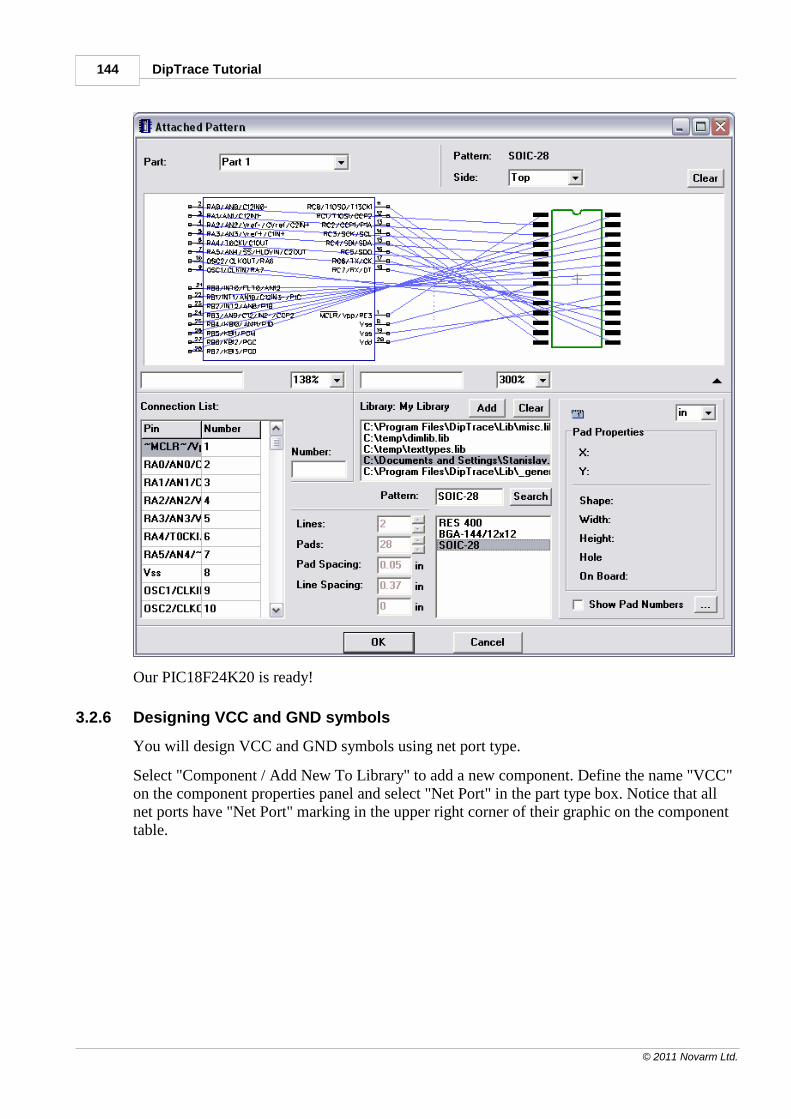
DipTrace Tutorial144
© 2011 Novarm Ltd.
Our PIC18F24K20 is ready!
3.2.6 Designing VCC and GND symbols
You will design VCC and GND symbols using net port type.
Select "Component / Add New To Library" to add a new component. Define the name "VCC"on the component properties panel and select "Net Port" in the part type box. Notice that allnet ports have "Net Port" marking in the upper right corner of their graphic on the componenttable.
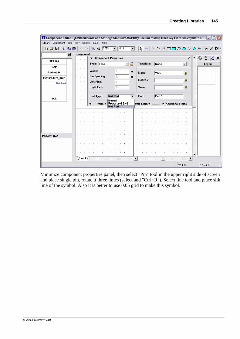
Creating Libraries 145
© 2011 Novarm Ltd.
Minimize component properties panel, then select "Pin" tool in the upper right side of screenand place single pin, rotate it three times (select and "Ctrl+R"). Select line tool and place silkline of the symbol. Also it is better to use 0.05 grid to make this symbol.
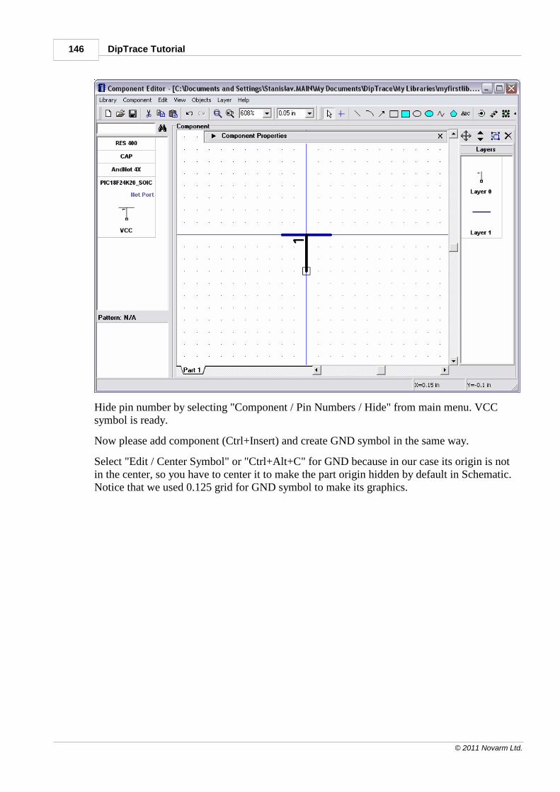
DipTrace Tutorial146
© 2011 Novarm Ltd.
Hide pin number by selecting "Component / Pin Numbers / Hide" from main menu. VCCsymbol is ready.
Now please add component (Ctrl+Insert) and create GND symbol in the same way.
Select "Edit / Center Symbol" or "Ctrl+Alt+C" for GND because in our case its origin is notin the center, so you have to center it to make the part origin hidden by default in Schematic.Notice that we used 0.125 grid for GND symbol to make its graphics.
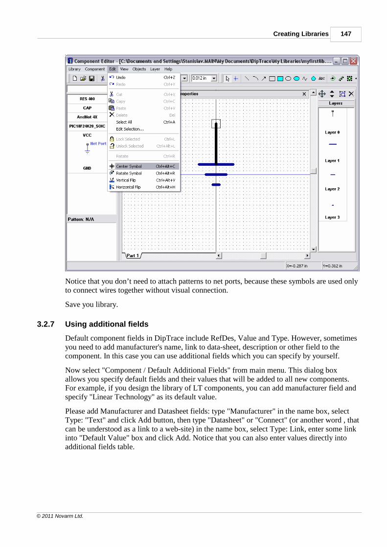
Creating Libraries 147
© 2011 Novarm Ltd.
Notice that you don’t need to attach patterns to net ports, because these symbols are used onlyto connect wires together without visual connection.
Save you library.
3.2.7 Using additional fields
Default component fields in DipTrace include RefDes, Value and Type. However, sometimesyou need to add manufacturer's name, link to data-sheet, description or other field to thecomponent. In this case you can use additional fields which you can specify by yourself.
Now select "Component / Default Additional Fields" from main menu. This dialog boxallows you specify default fields and their values that will be added to all new components.For example, if you design the library of LT components, you can add manufacturer field andspecify "Linear Technology" as its default value.
Please add Manufacturer and Datasheet fields: type "Manufacturer" in the name box, selectType: "Text" and click Add button, then type "Datasheet" or "Connect" (or another word , thatcan be understood as a link to a web-site) in the name box, select Type: Link, enter some linkinto "Default Value" box and click Add. Notice that you can also enter values directly intoadditional fields table.
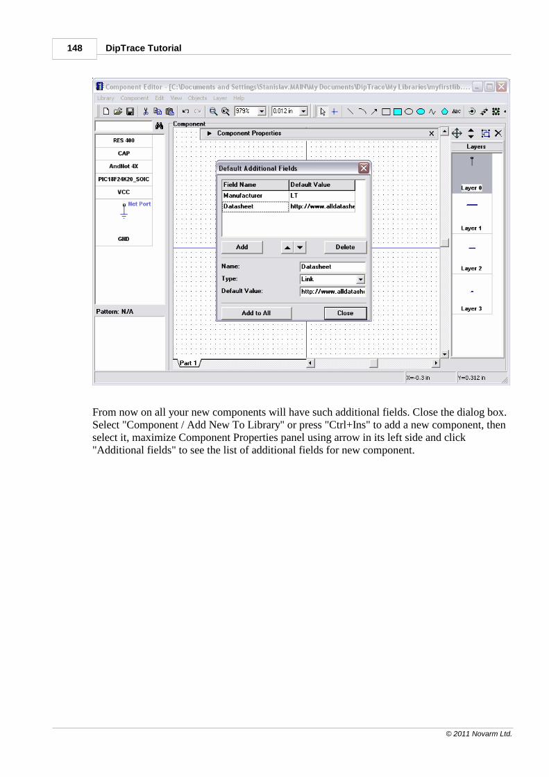
DipTrace Tutorial148
© 2011 Novarm Ltd.
From now on all your new components will have such additional fields. Close the dialog box.Select "Component / Add New To Library" or press "Ctrl+Ins" to add a new component, thenselect it, maximize Component Properties panel using arrow in its left side and click"Additional fields" to see the list of additional fields for new component.
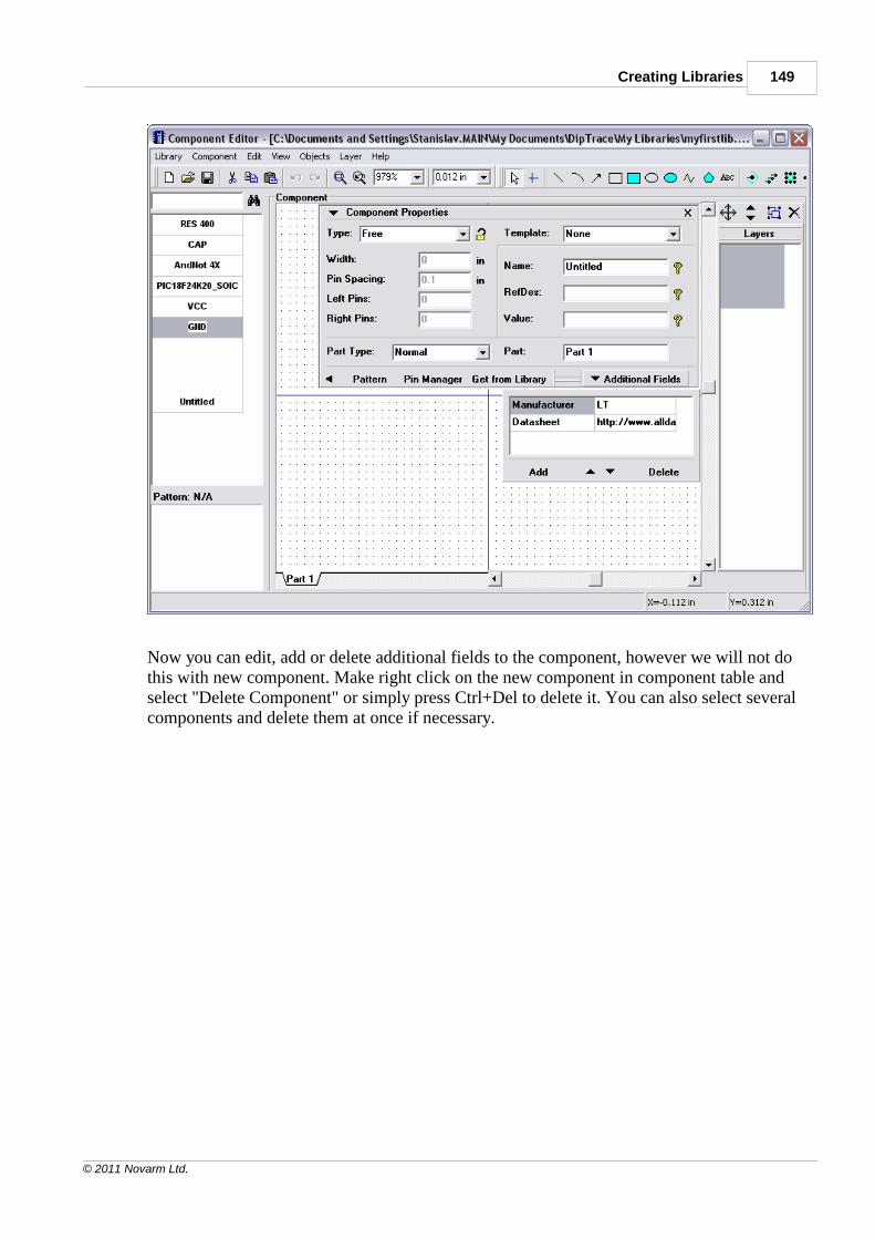
Creating Libraries 149
© 2011 Novarm Ltd.
Now you can edit, add or delete additional fields to the component, however we will not dothis with new component. Make right click on the new component in component table andselect "Delete Component" or simply press Ctrl+Del to delete it. You can also select severalcomponents and delete them at once if necessary.
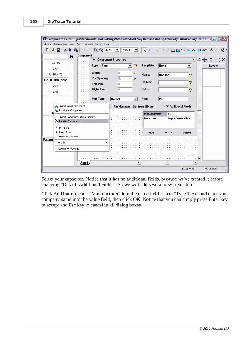
DipTrace Tutorial150
© 2011 Novarm Ltd.
Select your capacitor. Notice that it has no additional fields, because we've created it beforechanging "Default Additional Fields". So we will add several new fields to it.
Click Add button, enter "Manufacturer" into the name field, select "Type:Text" and enter yourcompany name into the value field, then click OK. Notice that you can simply press Enter keyto accept and Esc key to cancel in all dialog boxes.
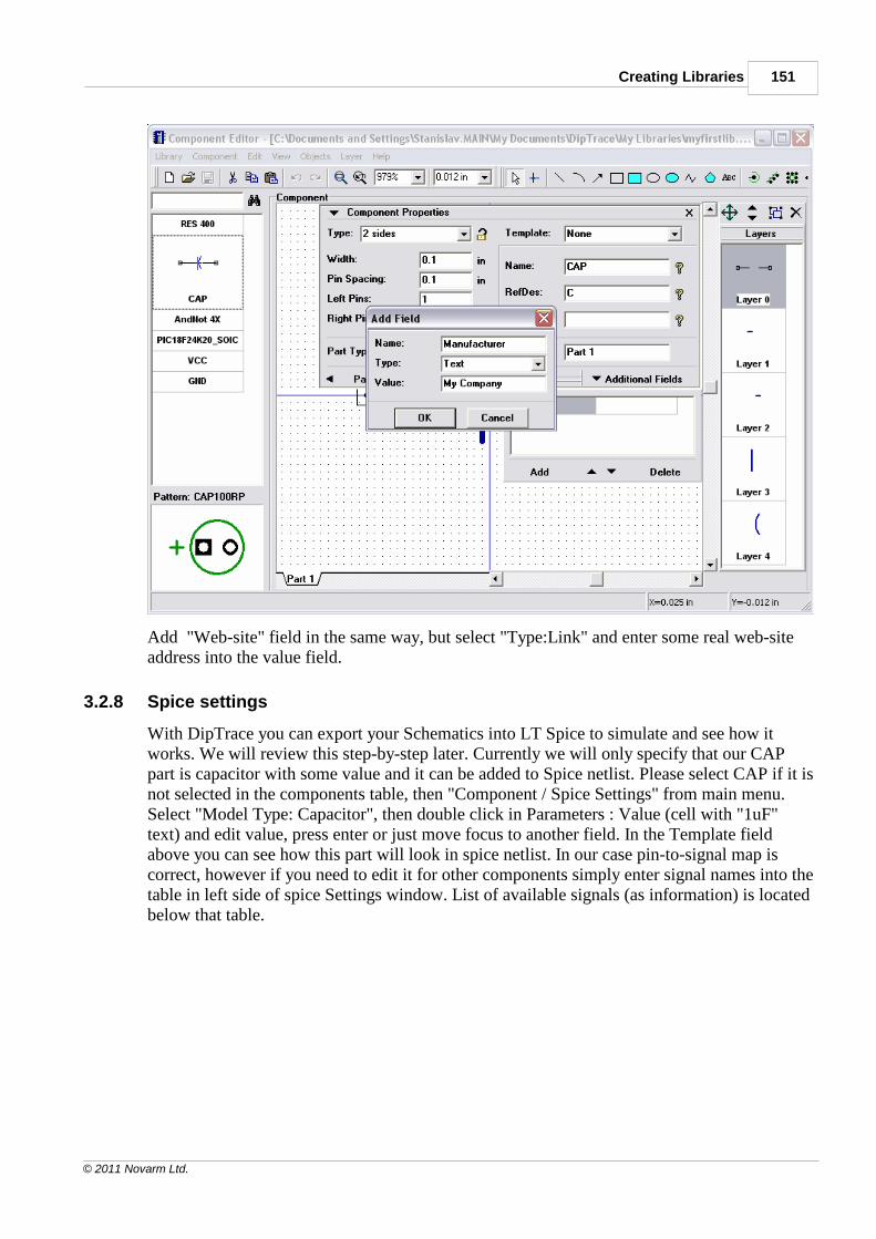
Creating Libraries 151
© 2011 Novarm Ltd.
Add "Web-site" field in the same way, but select "Type:Link" and enter some real web-siteaddress into the value field.
3.2.8 Spice settings
With DipTrace you can export your Schematics into LT Spice to simulate and see how itworks. We will review this step-by-step later. Currently we will only specify that our CAPpart is capacitor with some value and it can be added to Spice netlist. Please select CAP if it isnot selected in the components table, then "Component / Spice Settings" from main menu.Select "Model Type: Capacitor", then double click in Parameters : Value (cell with "1uF"text) and edit value, press enter or just move focus to another field. In the Template fieldabove you can see how this part will look in spice netlist. In our case pin-to-signal map iscorrect, however if you need to edit it for other components simply enter signal names into thetable in left side of spice Settings window. List of available signals (as information) is locatedbelow that table.
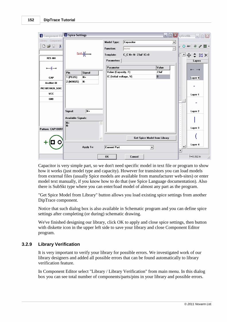
DipTrace Tutorial152
© 2011 Novarm Ltd.
Capacitor is very simple part, so we don't need specific model in text file or program to showhow it works (just model type and capacity). However for transistors you can load modelsfrom external files (usually Spice models are available from manufacturer web-sites) or entermodel text manually, if you know how to do that (see Spice Language documentation). Alsothere is SubSkt type where you can enter/load model of almost any part as the program.
"Get Spice Model from Library" button allows you load existing spice settings from anotherDipTrace component.
Notice that such dialog box is also available in Schematic program and you can define spicesettings after completing (or during) schematic drawing.
We've finished designing our library, click OK to apply and close spice settings, then buttonwith diskette icon in the upper left side to save your library and close Component Editorprogram.
3.2.9 Library Verification
It is very important to verify your library for possible errors. We investigated work of ourlibrary designers and added all possible errors that can be found automatically to libraryverification feature.
In Component Editor select "Library / Library Verification" from main menu. In this dialogbox you can see total number of components/parts/pins in your library and possible errors.
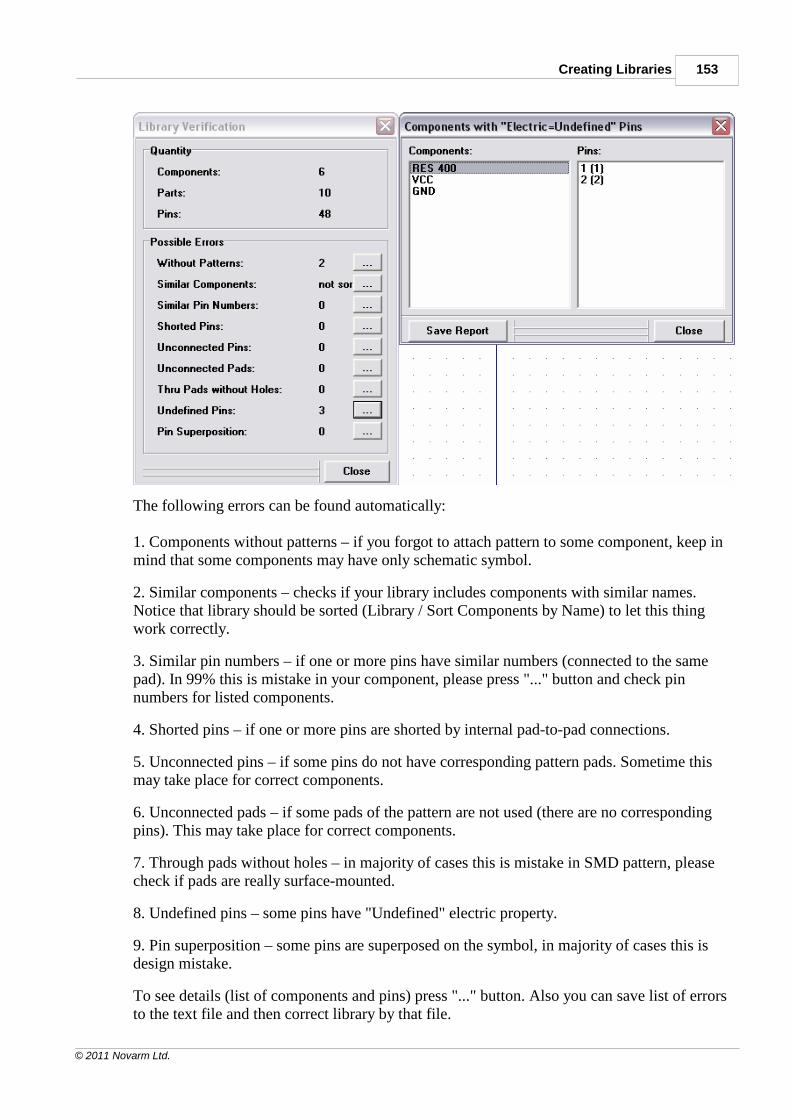
Creating Libraries 153
© 2011 Novarm Ltd.
The following errors can be found automatically:
1. Components without patterns – if you forgot to attach pattern to some component, keep inmind that some components may have only schematic symbol.
2. Similar components – checks if your library includes components with similar names.Notice that library should be sorted (Library / Sort Components by Name) to let this thingwork correctly.
3. Similar pin numbers – if one or more pins have similar numbers (connected to the samepad). In 99% this is mistake in your component, please press "..." button and check pinnumbers for listed components.
4. Shorted pins – if one or more pins are shorted by internal pad-to-pad connections.
5. Unconnected pins – if some pins do not have corresponding pattern pads. Sometime thismay take place for correct components.
6. Unconnected pads – if some pads of the pattern are not used (there are no correspondingpins). This may take place for correct components.
7. Through pads without holes – in majority of cases this is mistake in SMD pattern, pleasecheck if pads are really surface-mounted.
8. Undefined pins – some pins have "Undefined" electric property.
9. Pin superposition – some pins are superposed on the symbol, in majority of cases this isdesign mistake.
To see details (list of components and pins) press "..." button. Also you can save list of errorsto the text file and then correct library by that file.
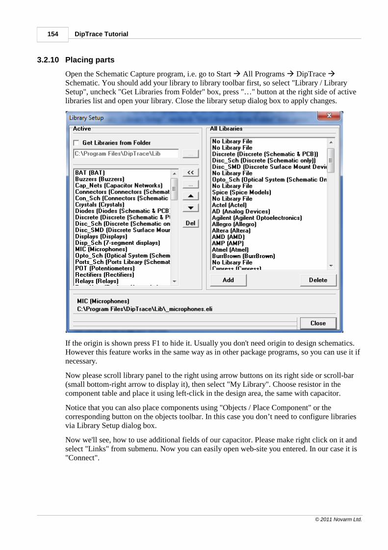
DipTrace Tutorial154
© 2011 Novarm Ltd.
3.2.10 Placing parts
Open the Schematic Capture program, i.e. go to Start All Programs DipTrace Schematic. You should add your library to library toolbar first, so select "Library / LibrarySetup", uncheck "Get Libraries from Folder" box, press "…" button at the right side of activelibraries list and open your library. Close the library setup dialog box to apply changes.
If the origin is shown press F1 to hide it. Usually you don't need origin to design schematics.However this feature works in the same way as in other package programs, so you can use it ifnecessary.
Now please scroll library panel to the right using arrow buttons on its right side or scroll-bar(small bottom-right arrow to display it), then select "My Library". Choose resistor in thecomponent table and place it using left-click in the design area, the same with capacitor.
Notice that you can also place components using "Objects / Place Component" or thecorresponding button on the objects toolbar. In this case you don’t need to configure librariesvia Library Setup dialog box.
Now we'll see, how to use additional fields of our capacitor. Please make right click on it andselect "Links" from submenu. Now you can easily open web-site you entered. In our case it is"Connect".
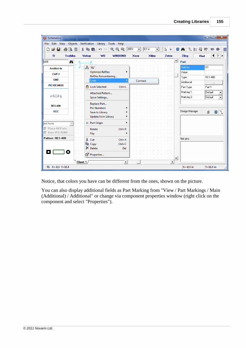
Creating Libraries 155
© 2011 Novarm Ltd.
Notice, that colors you have can be different from the ones, shown on the picture.
You can also display additional fields as Part Marking from "View / Part Markings / Main(Additional) / Additional" or change via component properties window (right click on thecomponent and select "Properties").
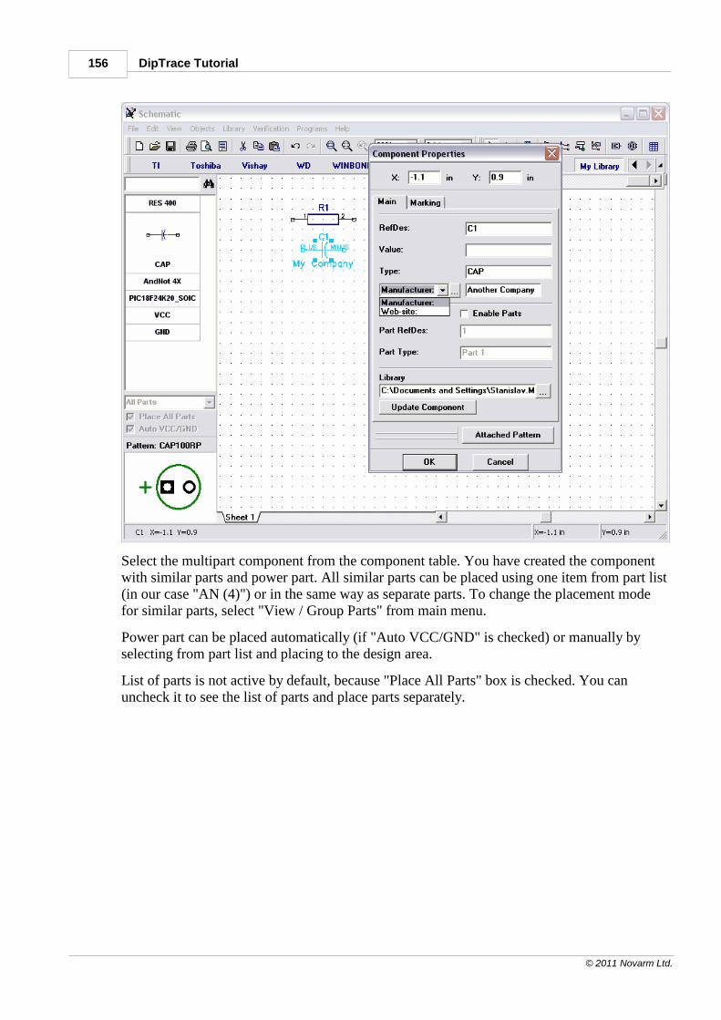
DipTrace Tutorial156
© 2011 Novarm Ltd.
Select the multipart component from the component table. You have created the componentwith similar parts and power part. All similar parts can be placed using one item from part list(in our case "AN (4)") or in the same way as separate parts. To change the placement modefor similar parts, select "View / Group Parts" from main menu.
Power part can be placed automatically (if "Auto VCC/GND" is checked) or manually byselecting from part list and placing to the design area.
List of parts is not active by default, because "Place All Parts" box is checked. You canuncheck it to see the list of parts and place parts separately.
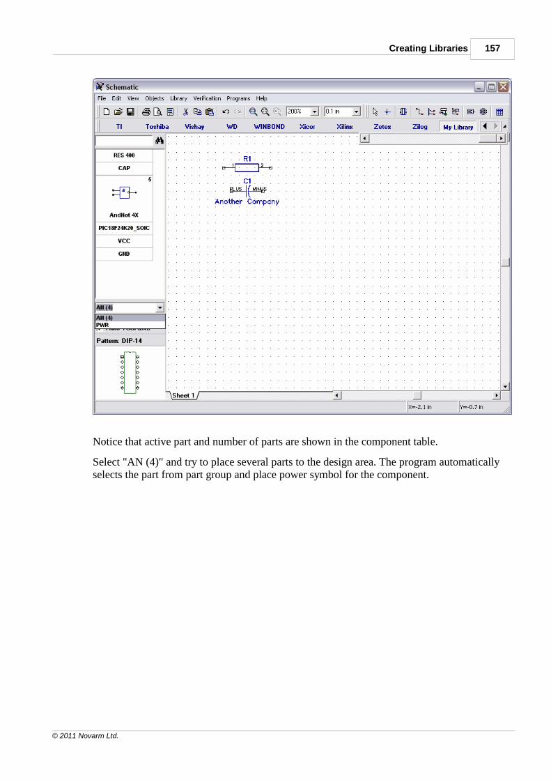
Creating Libraries 157
© 2011 Novarm Ltd.
Notice that active part and number of parts are shown in the component table.
Select "AN (4)" and try to place several parts to the design area. The program automaticallyselects the part from part group and place power symbol for the component.
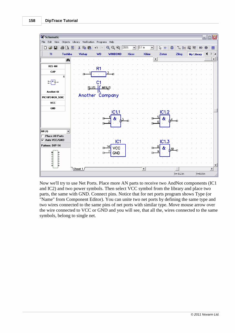
DipTrace Tutorial158
© 2011 Novarm Ltd.
Now we'll try to use Net Ports. Place more AN parts to receive two AndNot components (IC1and IC2) and two power symbols. Then select VCC symbol from the library and place twoparts, the same with GND. Connect pins. Notice that for net ports program shows Type (or"Name" from Component Editor). You can unite two net ports by defining the same type andtwo wires connected to the same pins of net ports with similar type. Move mouse arrow overthe wire connected to VCC or GND and you will see, that all the, wires connected to the samesymbols, belong to single net.
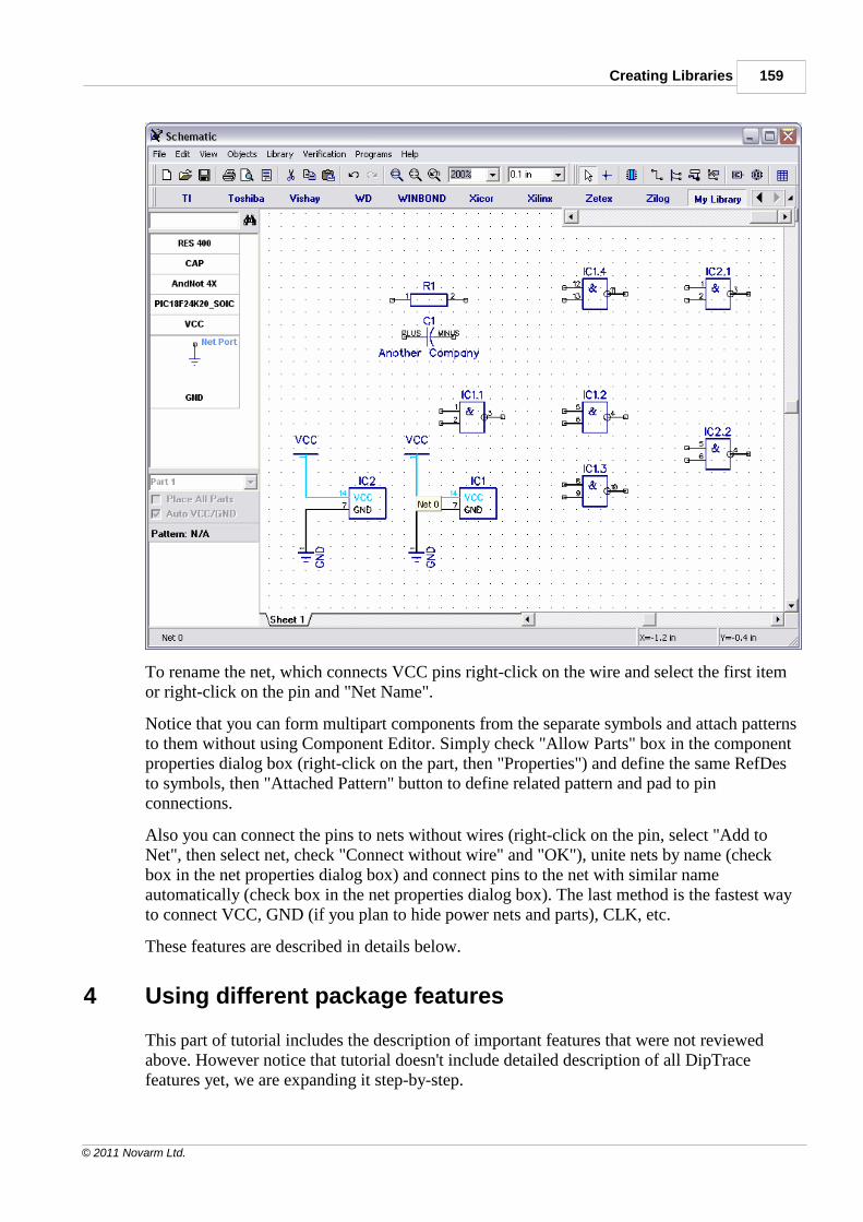
Creating Libraries 159
© 2011 Novarm Ltd.
To rename the net, which connects VCC pins right-click on the wire and select the first itemor right-click on the pin and "Net Name".
Notice that you can form multipart components from the separate symbols and attach patternsto them without using Component Editor. Simply check "Allow Parts" box in the componentproperties dialog box (right-click on the part, then "Properties") and define the same RefDesto symbols, then "Attached Pattern" button to define related pattern and pad to pinconnections.
Also you can connect the pins to nets without wires (right-click on the pin, select "Add toNet", then select net, check "Connect without wire" and "OK"), unite nets by name (checkbox in the net properties dialog box) and connect pins to the net with similar nameautomatically (check box in the net properties dialog box). The last method is the fastest wayto connect VCC, GND (if you plan to hide power nets and parts), CLK, etc.
These features are described in details below.
4 Using different package features
This part of tutorial includes the description of important features that were not reviewedabove. However notice that tutorial doesn't include detailed description of all DipTracefeatures yet, we are expanding it step-by-step.
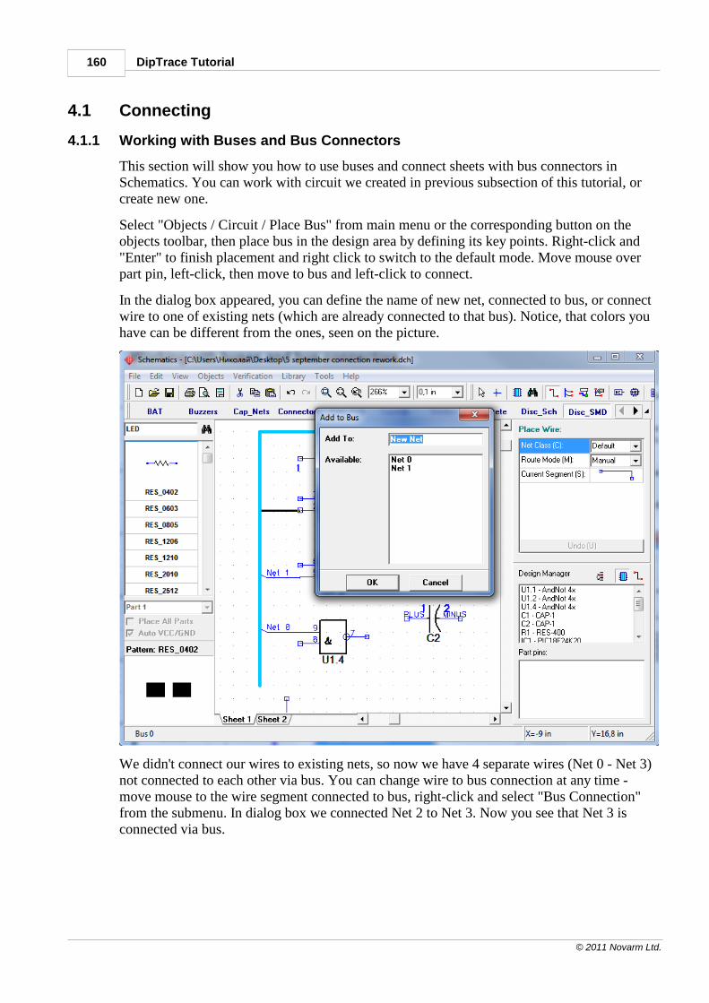
DipTrace Tutorial160
© 2011 Novarm Ltd.
4.1 Connecting
4.1.1 Working with Buses and Bus Connectors
This section will show you how to use buses and connect sheets with bus connectors inSchematics. You can work with circuit we created in previous subsection of this tutorial, orcreate new one.
Select "Objects / Circuit / Place Bus" from main menu or the corresponding button on theobjects toolbar, then place bus in the design area by defining its key points. Right-click and"Enter" to finish placement and right click to switch to the default mode. Move mouse overpart pin, left-click, then move to bus and left-click to connect.
In the dialog box appeared, you can define the name of new net, connected to bus, or connectwire to one of existing nets (which are already connected to that bus). Notice, that colors youhave can be different from the ones, seen on the picture.
We didn't connect our wires to existing nets, so now we have 4 separate wires (Net 0 - Net 3)not connected to each other via bus. You can change wire to bus connection at any time -move mouse to the wire segment connected to bus, right-click and select "Bus Connection"from the submenu. In dialog box we connected Net 2 to Net 3. Now you see that Net 3 isconnected via bus.
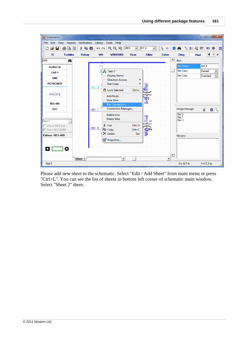
Using different package features 161
© 2011 Novarm Ltd.
Please add new sheet to the schematic. Select "Edit / Add Sheet" from main menu or press"Ctrl+L". You can see the list of sheets in bottom left corner of schematic main window.Select "Sheet 2" there.
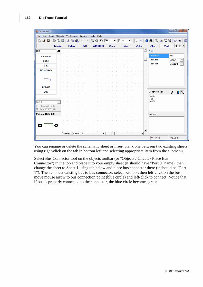
DipTrace Tutorial162
© 2011 Novarm Ltd.
You can rename or delete the schematic sheet or insert blank one between two existing sheetsusing right-click on the tab in bottom left and selecting appropriate item from the submenu.
Select Bus Connector tool on the objects toolbar (or "Objects / Circuit / Place BusConnector") in the top and place it to your empty sheet (it should have "Port 0" name), thenchange the sheet to Sheet 1 using tab below and place bus connector there (it should be "Port1"). Then connect existing bus to bus connector: select bus tool, then left-click on the bus,move mouse arrow to bus connection point (blue circle) and left-click to connect. Notice thatif bus is properly connected to the connector, the blue circle becomes green.
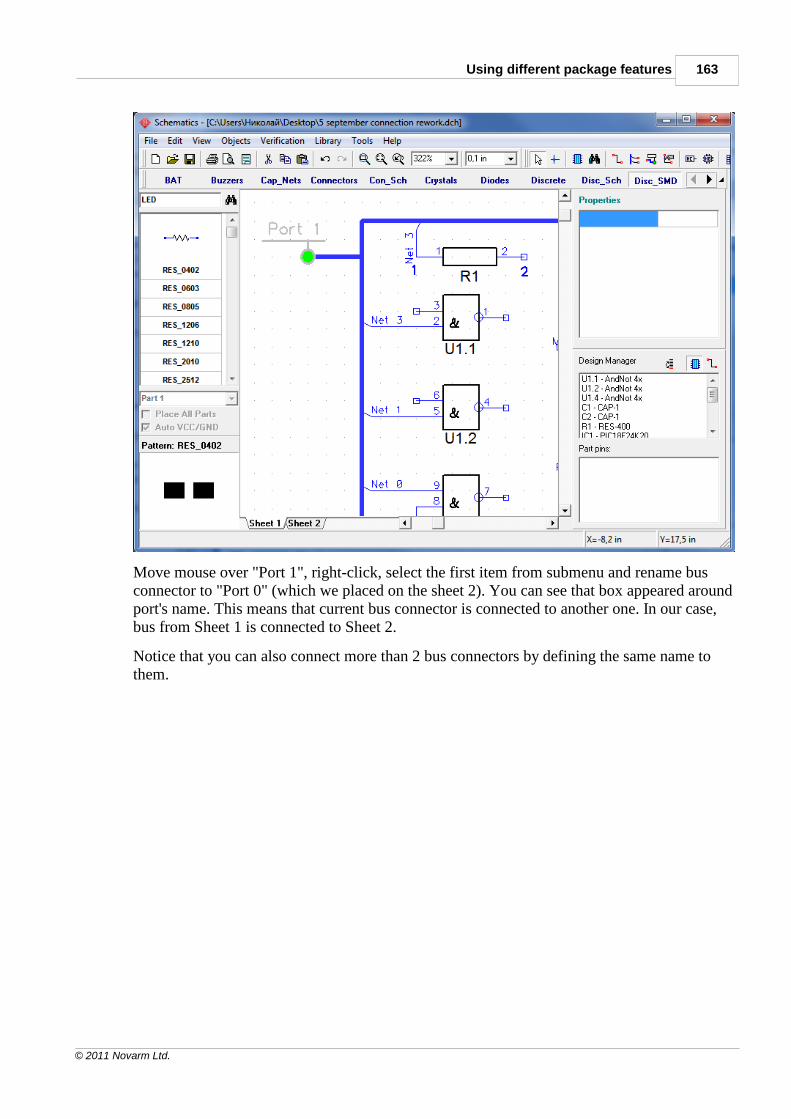
Using different package features 163
© 2011 Novarm Ltd.
Move mouse over "Port 1", right-click, select the first item from submenu and rename busconnector to "Port 0" (which we placed on the sheet 2). You can see that box appeared aroundport's name. This means that current bus connector is connected to another one. In our case,bus from Sheet 1 is connected to Sheet 2.
Notice that you can also connect more than 2 bus connectors by defining the same name tothem.
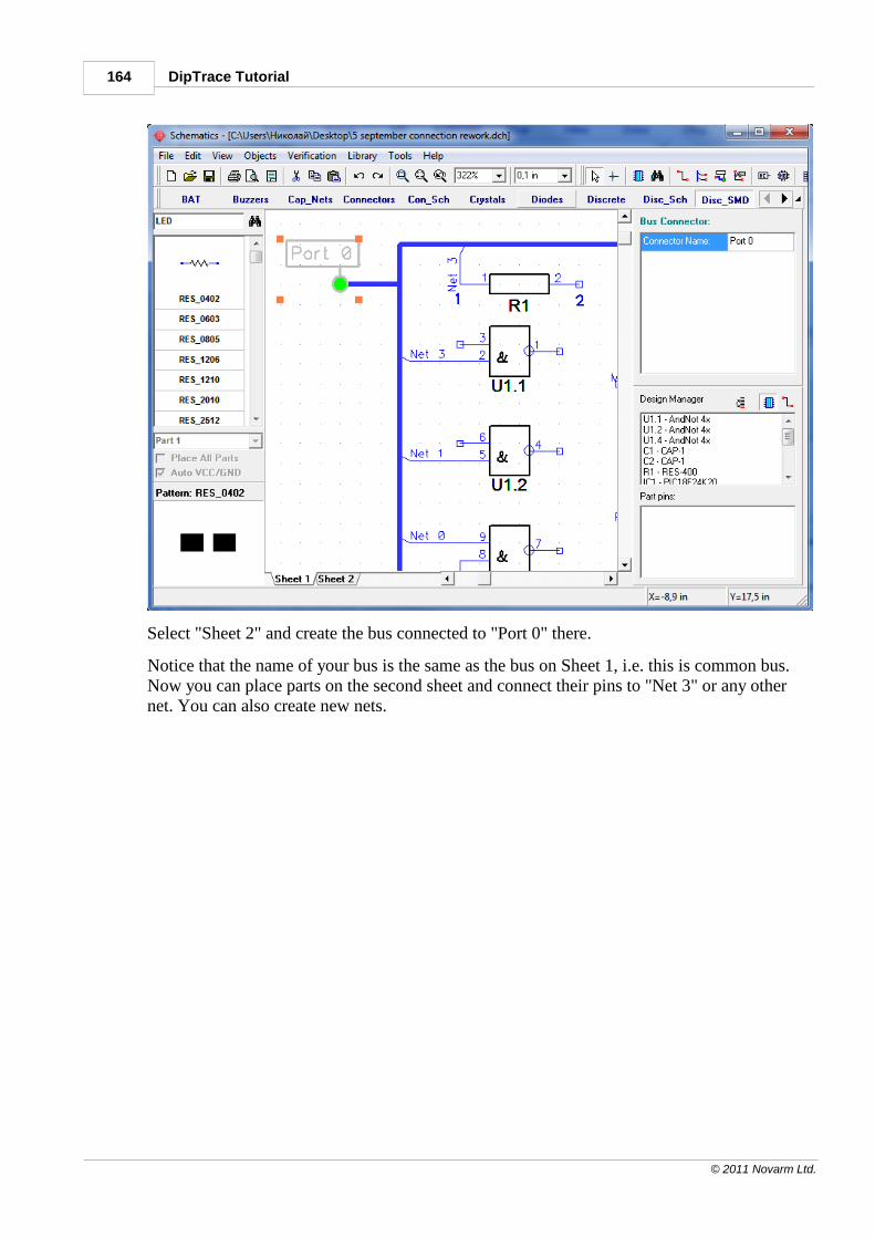
DipTrace Tutorial164
© 2011 Novarm Ltd.
Select "Sheet 2" and create the bus connected to "Port 0" there.
Notice that the name of your bus is the same as the bus on Sheet 1, i.e. this is common bus.Now you can place parts on the second sheet and connect their pins to "Net 3" or any othernet. You can also create new nets.
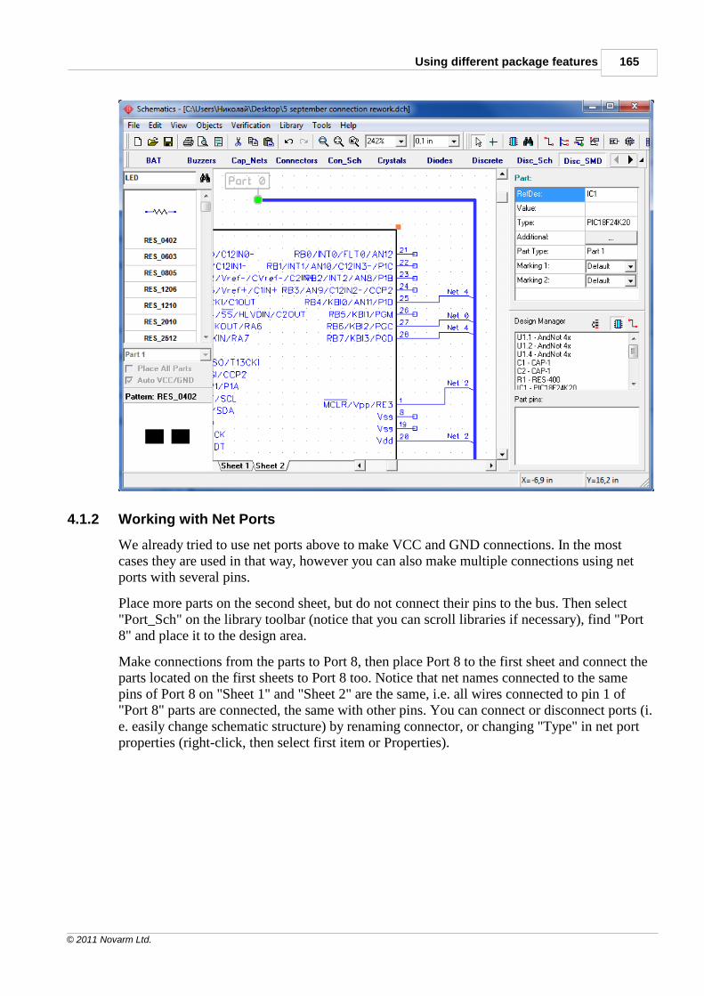
Using different package features 165
© 2011 Novarm Ltd.
4.1.2 Working with Net Ports
We already tried to use net ports above to make VCC and GND connections. In the mostcases they are used in that way, however you can also make multiple connections using netports with several pins.
Place more parts on the second sheet, but do not connect their pins to the bus. Then select"Port_Sch" on the library toolbar (notice that you can scroll libraries if necessary), find "Port8" and place it to the design area.
Make connections from the parts to Port 8, then place Port 8 to the first sheet and connect theparts located on the first sheets to Port 8 too. Notice that net names connected to the samepins of Port 8 on "Sheet 1" and "Sheet 2" are the same, i.e. all wires connected to pin 1 of"Port 8" parts are connected, the same with other pins. You can connect or disconnect ports (i.e. easily change schematic structure) by renaming connector, or changing "Type" in net portproperties (right-click, then select first item or Properties).
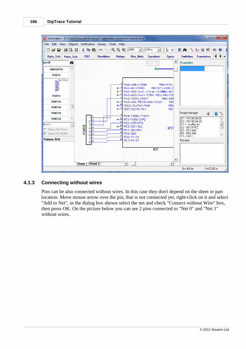
DipTrace Tutorial166
© 2011 Novarm Ltd.
4.1.3 Connecting without wires
Pins can be also connected without wires. In this case they don't depend on the sheet or partlocation. Move mouse arrow over the pin, that is not connected yet, right-click on it and select"Add to Net", in the dialog box shown select the net and check "Connect without Wire" box,then press OK. On the picture below you can see 2 pins connected to "Net 0" and "Net 1"without wires.
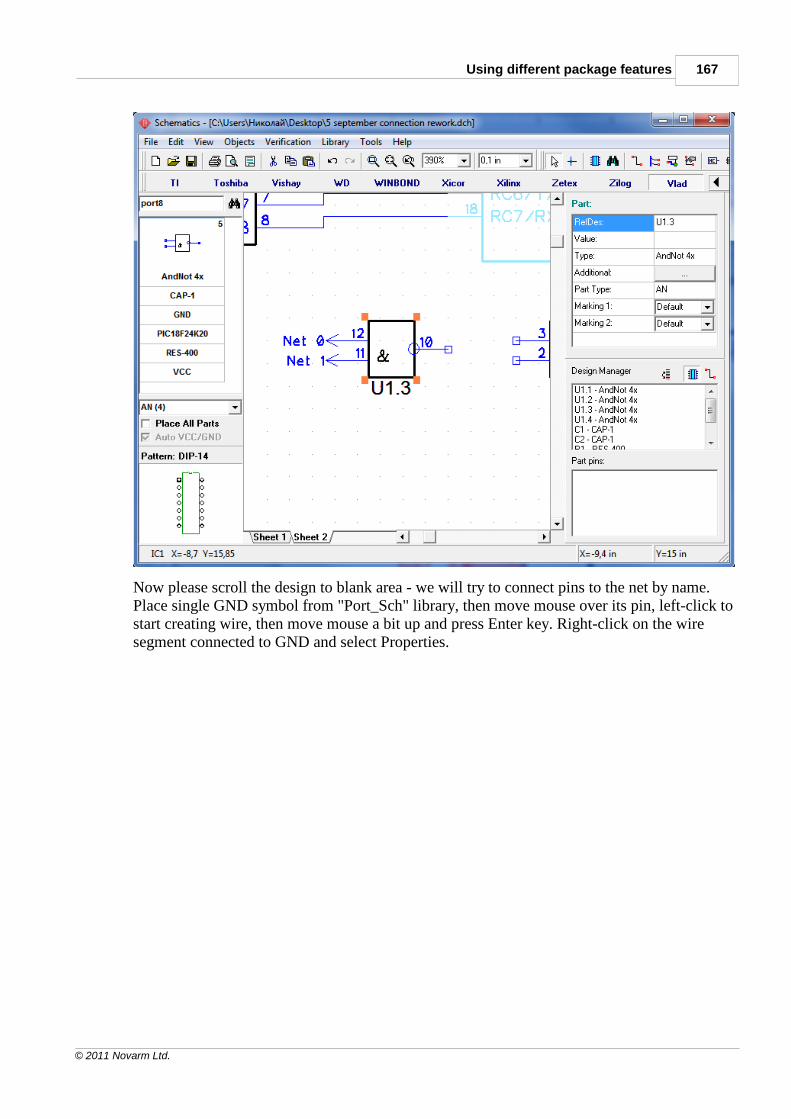
Using different package features 167
© 2011 Novarm Ltd.
Now please scroll the design to blank area - we will try to connect pins to the net by name.Place single GND symbol from "Port_Sch" library, then move mouse over its pin, left-click tostart creating wire, then move mouse a bit up and press Enter key. Right-click on the wiresegment connected to GND and select Properties.
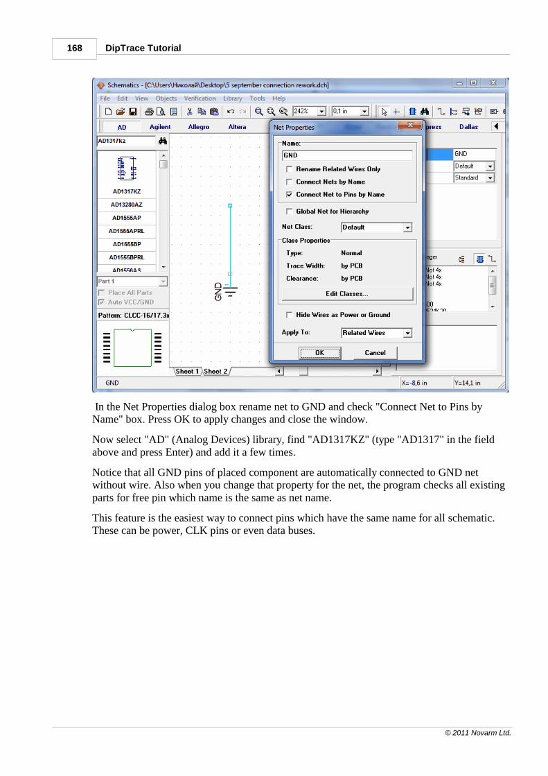
DipTrace Tutorial168
© 2011 Novarm Ltd.
In the Net Properties dialog box rename net to GND and check "Connect Net to Pins byName" box. Press OK to apply changes and close the window.
Now select "AD" (Analog Devices) library, find "AD1317KZ" (type "AD1317" in the fieldabove and press Enter) and add it a few times.
Notice that all GND pins of placed component are automatically connected to GND netwithout wire. Also when you change that property for the net, the program checks all existingparts for free pin which name is the same as net name.
This feature is the easiest way to connect pins which have the same name for all schematic.These can be power, CLK pins or even data buses.
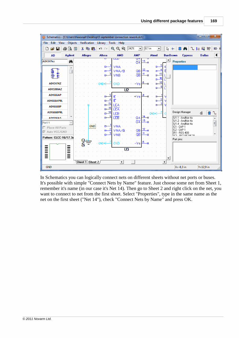
Using different package features 169
© 2011 Novarm Ltd.
In Schematics you can logically connect nets on different sheets without net ports or buses.It's possible with simple "Connect Nets by Name" feature. Just choose some net from Sheet 1,remember it's name (in our case it's Net 14). Then go to Sheet 2 and right click on the net, youwant to connect to net from the first sheet. Select "Properties", type in the same name as thenet on the first sheet ("Net 14"), check "Connect Nets by Name" and press OK.
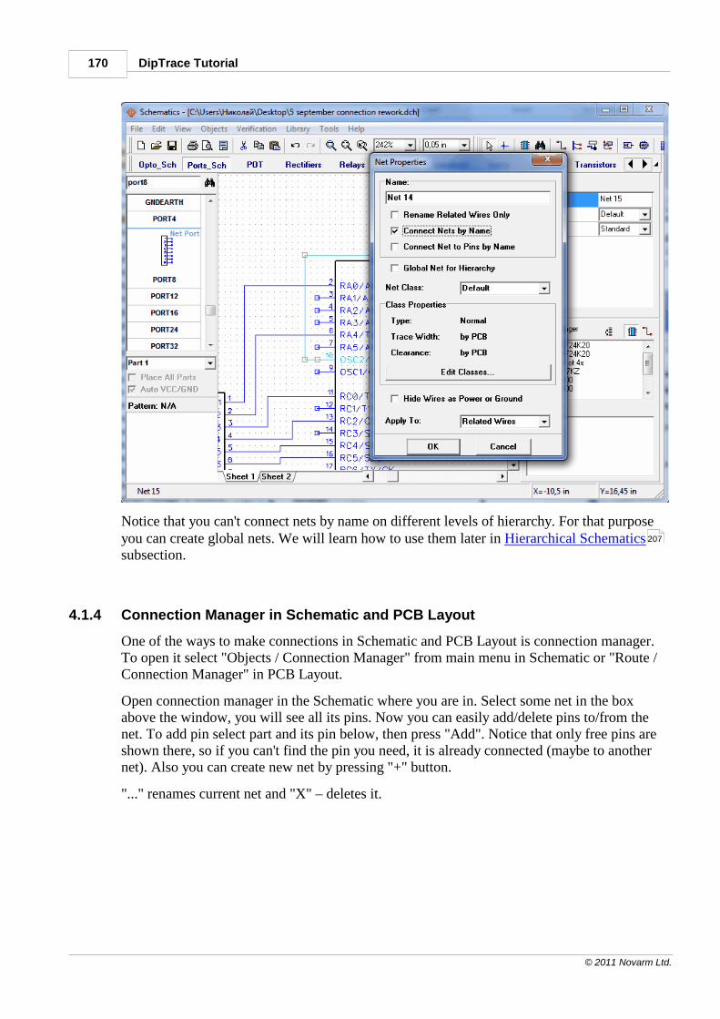
DipTrace Tutorial170
© 2011 Novarm Ltd.
Notice that you can't connect nets by name on different levels of hierarchy. For that purposeyou can create global nets. We will learn how to use them later in Hierarchical Schematicssubsection.
4.1.4 Connection Manager in Schematic and PCB Layout
One of the ways to make connections in Schematic and PCB Layout is connection manager.To open it select "Objects / Connection Manager" from main menu in Schematic or "Route /Connection Manager" in PCB Layout.
Open connection manager in the Schematic where you are in. Select some net in the boxabove the window, you will see all its pins. Now you can easily add/delete pins to/from thenet. To add pin select part and its pin below, then press "Add". Notice that only free pins areshown there, so if you can't find the pin you need, it is already connected (maybe to anothernet). Also you can create new net by pressing "+" button.
"..." renames current net and "X" – deletes it.
207
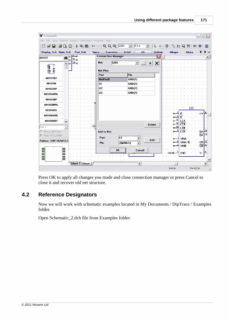
Using different package features 171
© 2011 Novarm Ltd.
Press OK to apply all changes you made and close connection manager or press Cancel toclose it and recover old net structure.
4.2 Reference Designators
Now we will work with schematic examples located in My Documents / DipTrace / Examplesfolder.
Open Schematic_2.dch file from Examples folder.

DipTrace Tutorial172
© 2011 Novarm Ltd.
On this Schematic you can see different types of pin connections made by our electronicengineer, however our goal is to make some experiments with reference designators to showyou how it works.
Current Schematic contains 23 capacitors from C1 to C24 (C19 is missing), but when tryingto edit you probably need to insert for example C5 somewhere. So please try to place acapacitor from the library you recently created (My Library). It will be our C5, but currently ithas C19 designator. Right-click on that capacitor and select the first item from submenu, enter"C5" and press OK. Program will show the warning message, but also suggest to rename thecomponent with shift of RefDes numeration. Choose “Yes”.
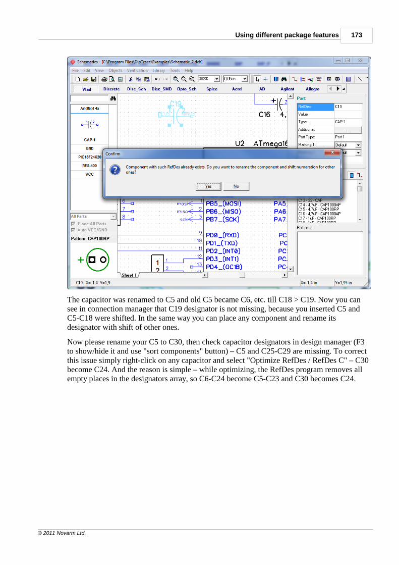
Using different package features 173
© 2011 Novarm Ltd.
The capacitor was renamed to C5 and old C5 became C6, etc. till C18 > C19. Now you cansee in connection manager that C19 designator is not missing, because you inserted C5 andC5-C18 were shifted. In the same way you can place any component and rename itsdesignator with shift of other ones.
Now please rename your C5 to C30, then check capacitor designators in design manager (F3to show/hide it and use "sort components" button) – C5 and C25-C29 are missing. To correctthis issue simply right-click on any capacitor and select "Optimize RefDes / RefDes C" – C30become C24. And the reason is simple – while optimizing, the RefDes program removes allempty places in the designators array, so C6-C24 become C5-C23 and C30 becomes C24.
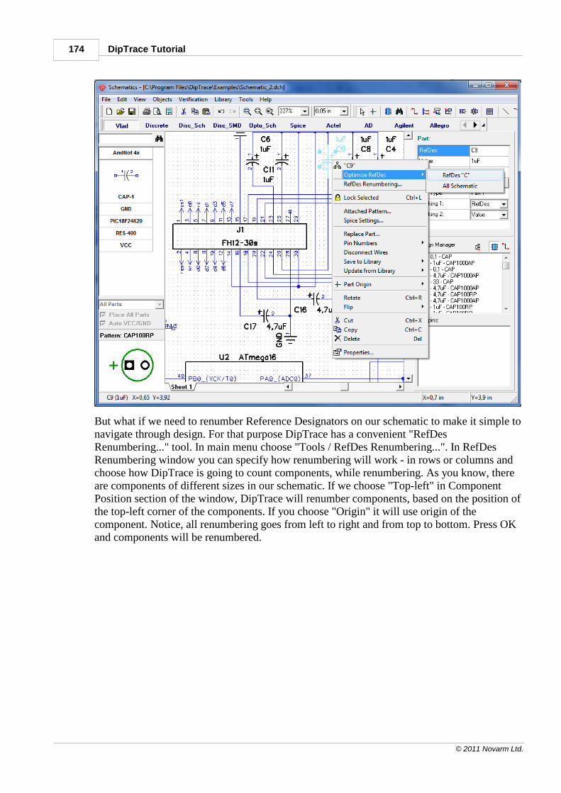
DipTrace Tutorial174
© 2011 Novarm Ltd.
But what if we need to renumber Reference Designators on our schematic to make it simple tonavigate through design. For that purpose DipTrace has a convenient "RefDesRenumbering..." tool. In main menu choose "Tools / RefDes Renumbering...". In RefDesRenumbering window you can specify how renumbering will work - in rows or columns andchoose how DipTrace is going to count components, while renumbering. As you know, thereare components of different sizes in our schematic. If we choose "Top-left" in ComponentPosition section of the window, DipTrace will renumber components, based on the position ofthe top-left corner of the components. If you choose "Origin" it will use origin of thecomponent. Notice, all renumbering goes from left to right and from top to bottom. Press OKand components will be renumbered.
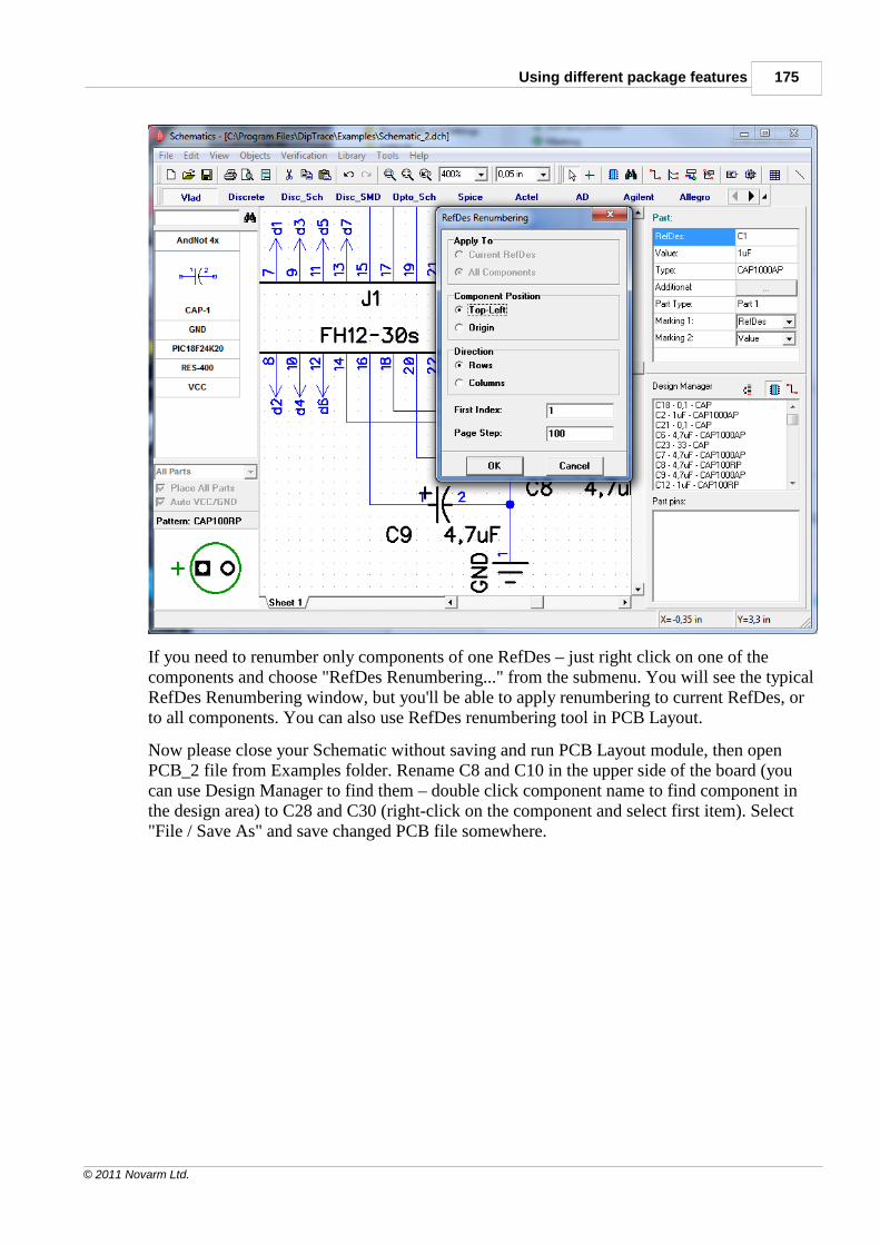
Using different package features 175
© 2011 Novarm Ltd.
If you need to renumber only components of one RefDes – just right click on one of thecomponents and choose "RefDes Renumbering..." from the submenu. You will see the typicalRefDes Renumbering window, but you'll be able to apply renumbering to current RefDes, orto all components. You can also use RefDes renumbering tool in PCB Layout.
Now please close your Schematic without saving and run PCB Layout module, then openPCB_2 file from Examples folder. Rename C8 and C10 in the upper side of the board (youcan use Design Manager to find them – double click component name to find component inthe design area) to C28 and C30 (right-click on the component and select first item). Select"File / Save As" and save changed PCB file somewhere.
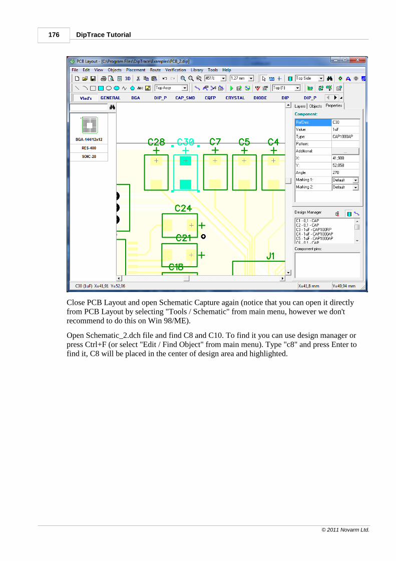
DipTrace Tutorial176
© 2011 Novarm Ltd.
Close PCB Layout and open Schematic Capture again (notice that you can open it directlyfrom PCB Layout by selecting "Tools / Schematic" from main menu, however we don'trecommend to do this on Win 98/ME).
Open Schematic_2.dch file and find C8 and C10. To find it you can use design manager orpress Ctrl+F (or select "Edit / Find Object" from main menu). Type "c8" and press Enter tofind it, C8 will be placed in the center of design area and highlighted.
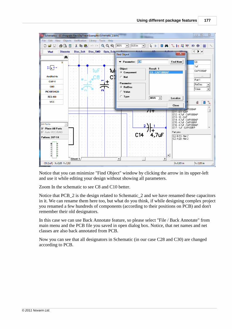
Using different package features 177
© 2011 Novarm Ltd.
Notice that you can minimize "Find Object" window by clicking the arrow in its upper-leftand use it while editing your design without showing all parameters.
Zoom In the schematic to see C8 and C10 better.
Notice that PCB_2 is the design related to Schematic_2 and we have renamed these capacitorsin it. We can rename them here too, but what do you think, if while designing complex projectyou renamed a few hundreds of components (according to their positions on PCB) and don'tremember their old designators.
In this case we can use Back Annotate feature, so please select "File / Back Annotate" frommain menu and the PCB file you saved in open dialog box. Notice, that net names and netclasses are also back annotated from PCB.
Now you can see that all designators in Schematic (in our case C28 and C30) are changedaccording to PCB.
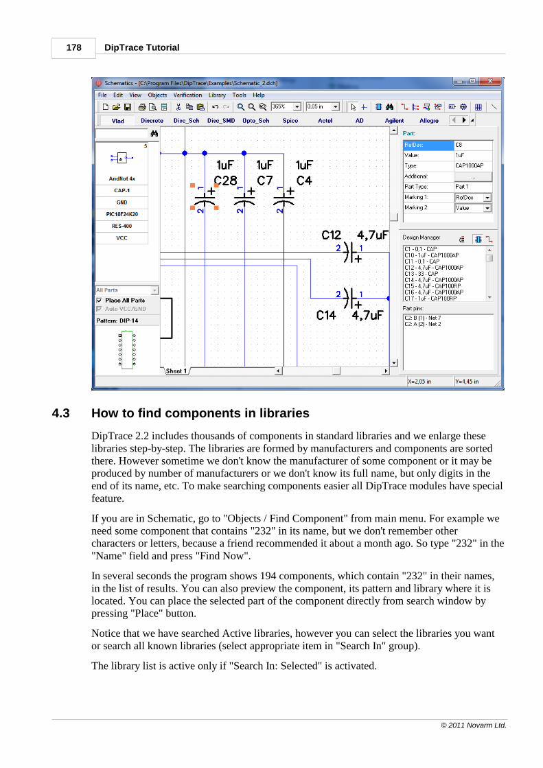
DipTrace Tutorial178
© 2011 Novarm Ltd.
4.3 How to find components in libraries
DipTrace 2.2 includes thousands of components in standard libraries and we enlarge theselibraries step-by-step. The libraries are formed by manufacturers and components are sortedthere. However sometime we don't know the manufacturer of some component or it may beproduced by number of manufacturers or we don't know its full name, but only digits in theend of its name, etc. To make searching components easier all DipTrace modules have specialfeature.
If you are in Schematic, go to "Objects / Find Component" from main menu. For example weneed some component that contains "232" in its name, but we don't remember othercharacters or letters, because a friend recommended it about a month ago. So type "232" in the"Name" field and press "Find Now".
In several seconds the program shows 194 components, which contain "232" in their names,in the list of results. You can also preview the component, its pattern and library where it islocated. You can place the selected part of the component directly from search window bypressing "Place" button.
Notice that we have searched Active libraries, however you can select the libraries you wantor search all known libraries (select appropriate item in "Search In" group).
The library list is active only if "Search In: Selected" is activated.
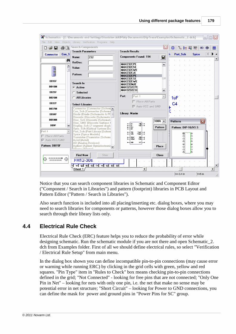
Using different package features 179
© 2011 Novarm Ltd.
Notice that you can search component libraries in Schematic and Component Editor("Component / Search in Libraries") and pattern (footprint) libraries in PCB Layout andPattern Editor ("Pattern / Search in Libraries").
Also search function is included into all placing/inserting etc. dialog boxes, where you mayneed to search libraries for components or patterns, however those dialog boxes allow you tosearch through their library lists only.
4.4 Electrical Rule Check
Electrical Rule Check (ERC) feature helps you to reduce the probability of error whiledesigning schematic. Run the schematic module if you are not there and open Schematic_2.dch from Examples folder. First of all we should define electrical rules, so select "Verification/ Electrical Rule Setup" from main menu.
In the dialog box shown you can define incompatible pin-to-pin connections (may cause erroror warning while running ERC) by clicking in the grid cells with green, yellow and redsquares. "Pin Type" item in "Rules to Check" box means checking pin-to-pin connectionsdefined in the grid; "Not Connected" - looking for free pins that are not connected; "Only OnePin in Net" – looking for nets with only one pin, i.e. the net that make no sense may bepotential error in net structure; "Short Circuit" – looking for Power to GND connections, youcan define the mask for power and ground pins in "Power Pins for SC" group.
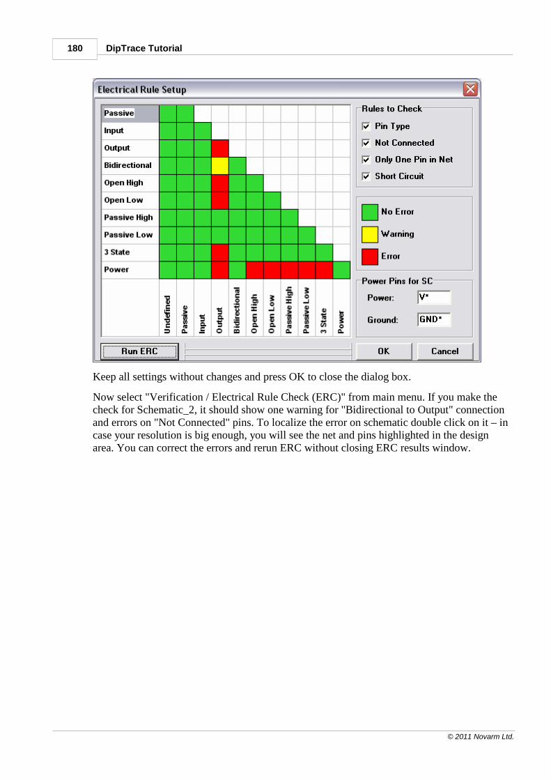
DipTrace Tutorial180
© 2011 Novarm Ltd.
Keep all settings without changes and press OK to close the dialog box.
Now select "Verification / Electrical Rule Check (ERC)" from main menu. If you make thecheck for Schematic_2, it should show one warning for "Bidirectional to Output" connectionand errors on "Not Connected" pins. To localize the error on schematic double click on it – incase your resolution is big enough, you will see the net and pins highlighted in the designarea. You can correct the errors and rerun ERC without closing ERC results window.
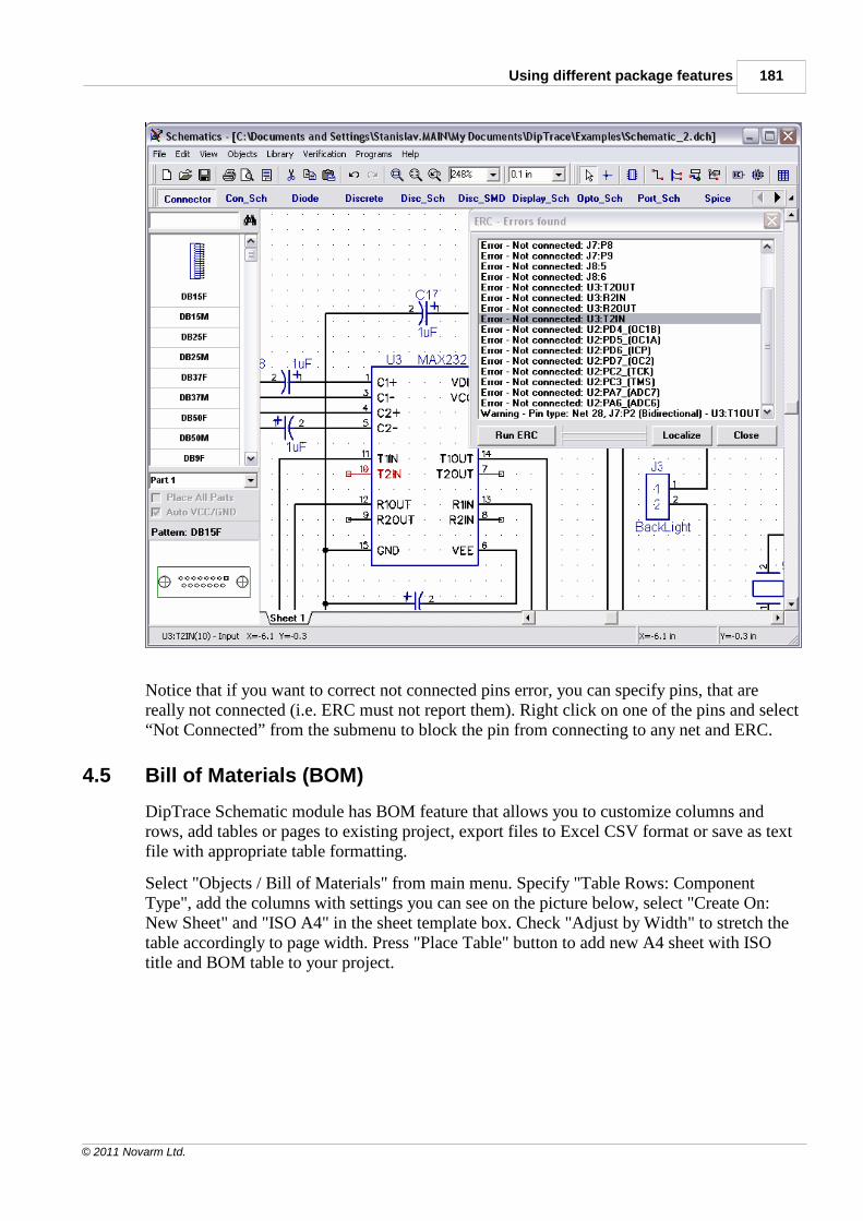
Using different package features 181
© 2011 Novarm Ltd.
Notice that if you want to correct not connected pins error, you can specify pins, that arereally not connected (i.e. ERC must not report them). Right click on one of the pins and select“Not Connected” from the submenu to block the pin from connecting to any net and ERC.
4.5 Bill of Materials (BOM)
DipTrace Schematic module has BOM feature that allows you to customize columns androws, add tables or pages to existing project, export files to Excel CSV format or save as textfile with appropriate table formatting.
Select "Objects / Bill of Materials" from main menu. Specify "Table Rows: ComponentType", add the columns with settings you can see on the picture below, select "Create On:New Sheet" and "ISO A4" in the sheet template box. Check "Adjust by Width" to stretch thetable accordingly to page width. Press "Place Table" button to add new A4 sheet with ISOtitle and BOM table to your project.
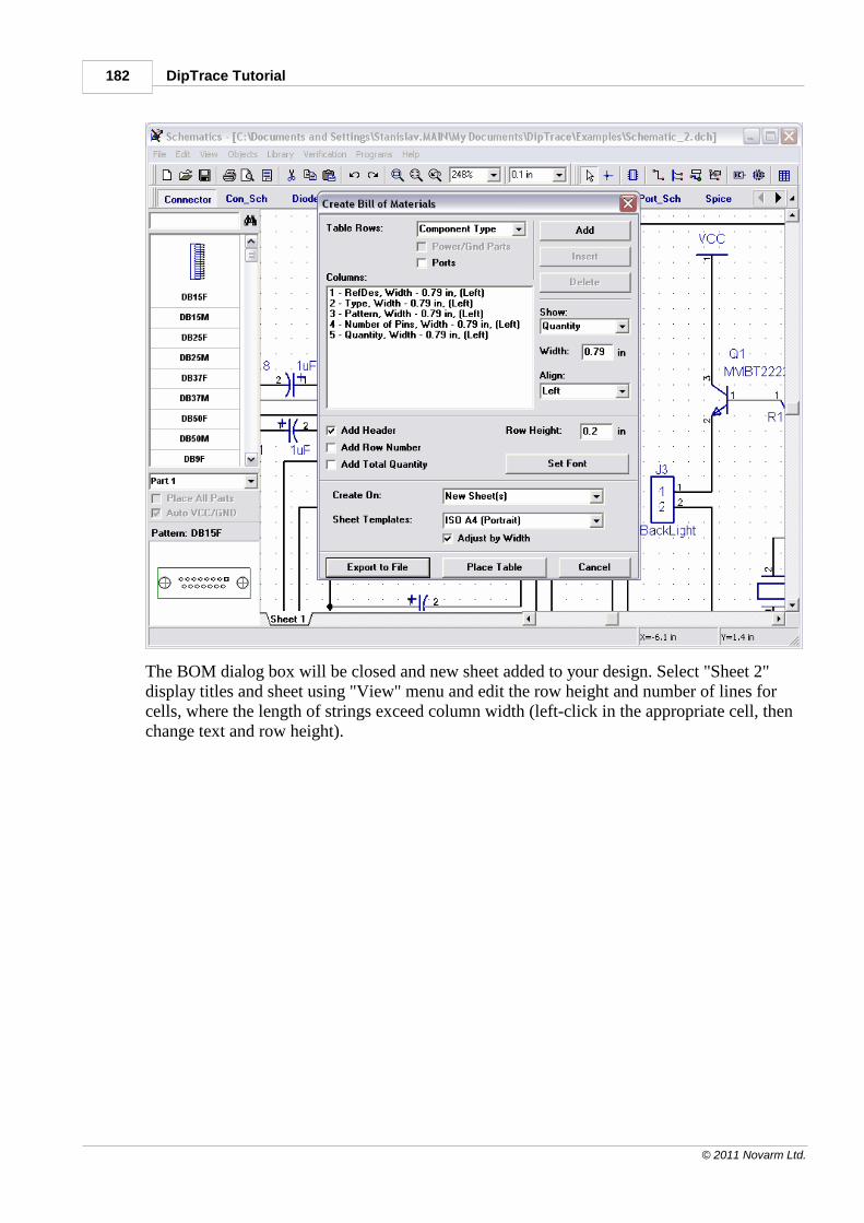
DipTrace Tutorial182
© 2011 Novarm Ltd.
The BOM dialog box will be closed and new sheet added to your design. Select "Sheet 2"display titles and sheet using "View" menu and edit the row height and number of lines forcells, where the length of strings exceed column width (left-click in the appropriate cell, thenchange text and row height).
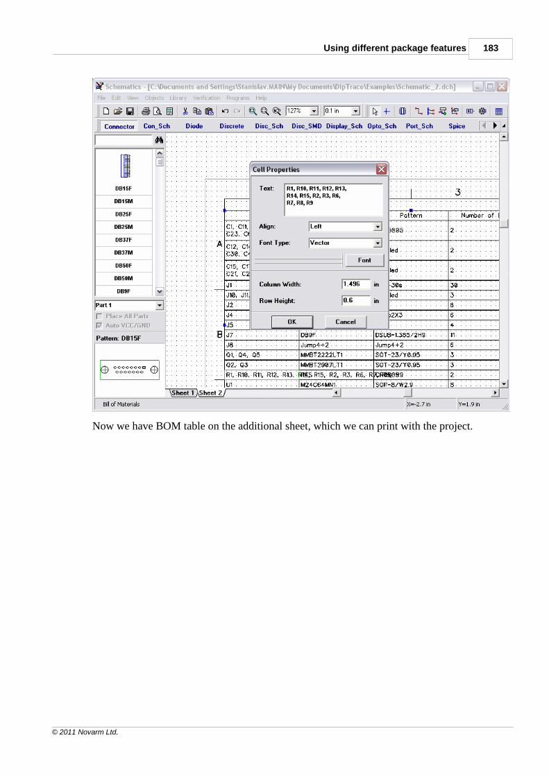
Using different package features 183
© 2011 Novarm Ltd.
Now we have BOM table on the additional sheet, which we can print with the project.
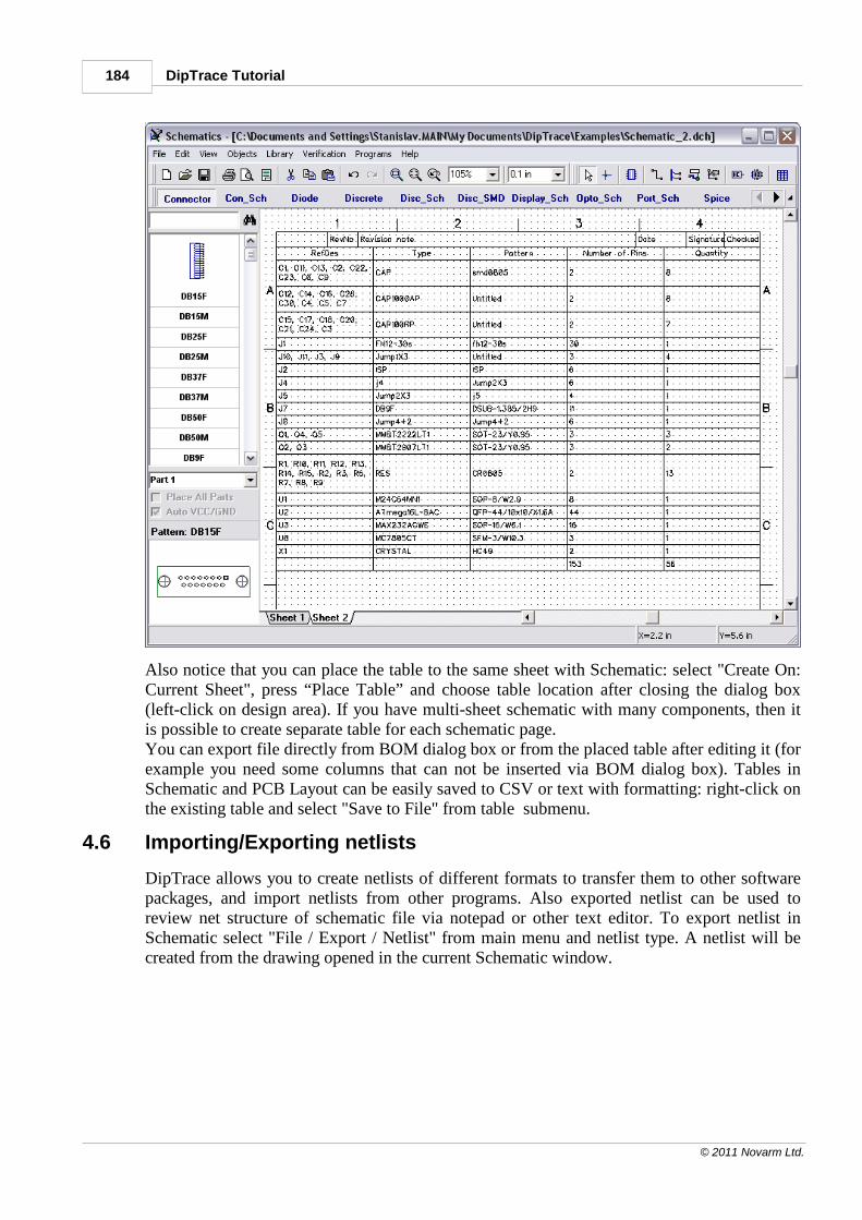
DipTrace Tutorial184
© 2011 Novarm Ltd.
Also notice that you can place the table to the same sheet with Schematic: select "Create On:Current Sheet", press “Place Table” and choose table location after closing the dialog box(left-click on design area). If you have multi-sheet schematic with many components, then itis possible to create separate table for each schematic page.You can export file directly from BOM dialog box or from the placed table after editing it (forexample you need some columns that can not be inserted via BOM dialog box). Tables inSchematic and PCB Layout can be easily saved to CSV or text with formatting: right-click onthe existing table and select "Save to File" from table submenu.
4.6 Importing/Exporting netlists
DipTrace allows you to create netlists of different formats to transfer them to other softwarepackages, and import netlists from other programs. Also exported netlist can be used toreview net structure of schematic file via notepad or other text editor. To export netlist inSchematic select "File / Export / Netlist" from main menu and netlist type. A netlist will becreated from the drawing opened in the current Schematic window.
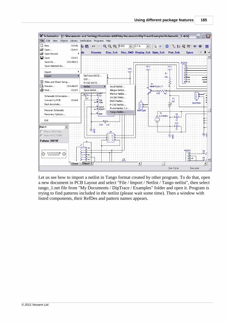
Using different package features 185
© 2011 Novarm Ltd.
Let us see how to import a netlist in Tango format created by other program. To do that, opena new document in PCB Layout and select "File / Import / Netlist / Tango netlist", then selecttango_1.net file from "My Documents / DipTrace / Examples" folder and open it. Program istrying to find patterns included in the netlist (please wait some time). Then a window withlisted components, their RefDes and pattern names appears.
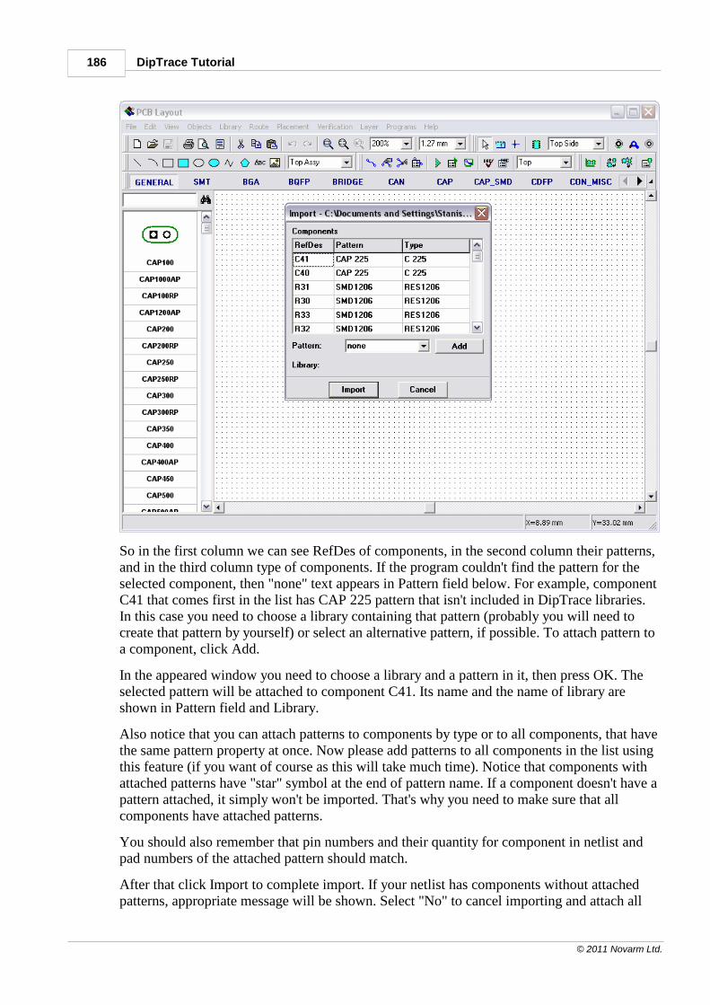
DipTrace Tutorial186
© 2011 Novarm Ltd.
So in the first column we can see RefDes of components, in the second column their patterns,and in the third column type of components. If the program couldn't find the pattern for theselected component, then "none" text appears in Pattern field below. For example, componentC41 that comes first in the list has CAP 225 pattern that isn't included in DipTrace libraries.In this case you need to choose a library containing that pattern (probably you will need tocreate that pattern by yourself) or select an alternative pattern, if possible. To attach pattern toa component, click Add.
In the appeared window you need to choose a library and a pattern in it, then press OK. Theselected pattern will be attached to component С41. Its name and the name of library areshown in Pattern field and Library.
Also notice that you can attach patterns to components by type or to all components, that havethe same pattern property at once. Now please add patterns to all components in the list usingthis feature (if you want of course as this will take much time). Notice that components withattached patterns have "star" symbol at the end of pattern name. If a component doesn't have apattern attached, it simply won't be imported. That's why you need to make sure that allcomponents have attached patterns.
You should also remember that pin numbers and their quantity for component in netlist andpad numbers of the attached pattern should match.
After that click Import to complete import. If your netlist has components without attachedpatterns, appropriate message will be shown. Select "No" to cancel importing and attach all
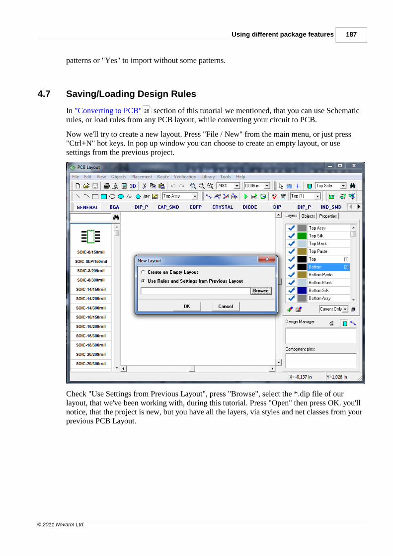
Using different package features 187
© 2011 Novarm Ltd.
patterns or "Yes" to import without some patterns.
4.7 Saving/Loading Design Rules
In "Converting to PCB" section of this tutorial we mentioned, that you can use Schematicrules, or load rules from any PCB layout, while converting your circuit to PCB.
Now we'll try to create a new layout. Press "File / New" from the main menu, or just press"Ctrl+N" hot keys. In pop up window you can choose to create an empty layout, or usesettings from the previous project.
Check "Use Settings from Previous Layout", press "Browse", select the *.dip file of ourlayout, that we've been working with, during this tutorial. Press "Open" then press OK. you'llnotice, that the project is new, but you have all the layers, via styles and net classes from yourprevious PCB Layout.
28
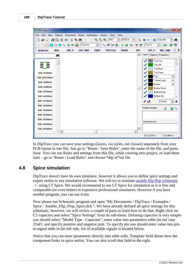
DipTrace Tutorial188
© 2011 Novarm Ltd.
In DipTrace you can save your settings (layers, via styles, net classes) separately from yourPCB layout in one file. Just go to "Route / Save Rules", enter the name of the file, and pressSave. You can use Rules and settings from this file, while creating new project, or load themlater – go to "Route / Load Rules" and choose *dip or*rul file.
4.8 Spice simulation
DipTrace doesn't have its own simulator, however it allows you to define spice settings andexport netlist to any simulation software. We will try to simulate astable flip-flop schematic
using LT Spice. We would recommend to use LT Spice for simulation as it is free andcomparable (or even better) to expensive professional simulators. However if you haveanother program, you can use it too.
Now please run Schematic program and open "My Documents / DipTrace / Examples /Spice / Astable_Flip_Flop_Spice.dch ". We have already defined all spice settings for thisschematic, however, we will review a couple of parts to learn how to do that. Right click onC2 capacitor and select "Spice Settings" from its sub-menu. Defining capacitor is very simple:you should select "Model Type : Capacitor", enter value into parameters table (in our case22uF) and specify positive and negative pins. To specify pin you should enter value into pin-to-signal table in the left side, list of available signals is located below.
Notice that you can enter parameters directly into table cells. Template field shows how thecomponent looks in spice netlist. You can also scroll that field to the right.
5
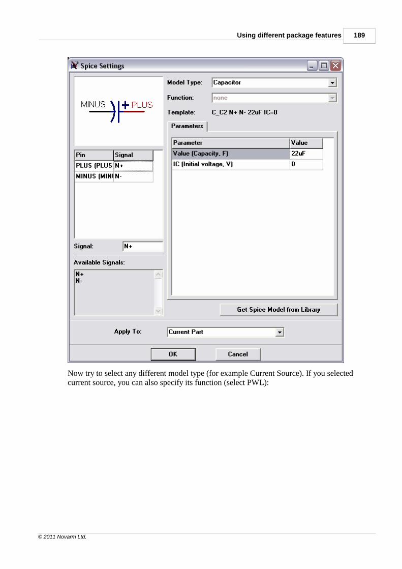
Using different package features 189
© 2011 Novarm Ltd.
Now try to select any different model type (for example Current Source). If you selectedcurrent source, you can also specify its function (select PWL):
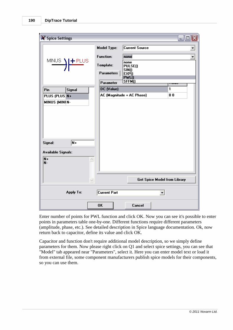
DipTrace Tutorial190
© 2011 Novarm Ltd.
Enter number of points for PWL function and click OK. Now you can see it's possible to enterpoints in parameters table one-by-one. Different functions require different parameters(amplitude, phase, etc.). See detailed description in Spice language documentation. Ok, nowreturn back to capacitor, define its value and click OK.
Capacitor and function don't require additional model description, so we simply defineparameters for them. Now please right click on Q1 and select spice settings, you can see that"Model" tab appeared near "Parameters", select it. Here you can enter model text or load itfrom external file, some component manufacturers publish spice models for their components,so you can use them.
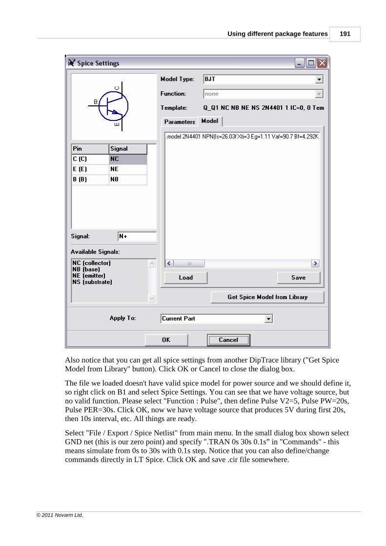
Using different package features 191
© 2011 Novarm Ltd.
Also notice that you can get all spice settings from another DipTrace library ("Get SpiceModel from Library" button). Click OK or Cancel to close the dialog box.
The file we loaded doesn't have valid spice model for power source and we should define it,so right click on B1 and select Spice Settings. You can see that we have voltage source, butno valid function. Please select "Function : Pulse", then define Pulse V2=5, Pulse PW=20s,Pulse PER=30s. Click OK, now we have voltage source that produces 5V during first 20s,then 10s interval, etc. All things are ready.
Select "File / Export / Spice Netlist" from main menu. In the small dialog box shown selectGND net (this is our zero point) and specify ".TRAN 0s 30s 0.1s” in "Commands" - thismeans simulate from 0s to 30s with 0.1s step. Notice that you can also define/changecommands directly in LT Spice. Click OK and save .cir file somewhere.
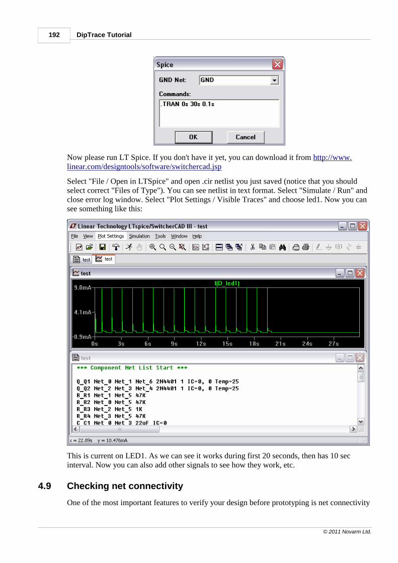
DipTrace Tutorial192
© 2011 Novarm Ltd.
Now please run LT Spice. If you don't have it yet, you can download it from http://www.linear.com/designtools/software/switchercad.jsp
Select "File / Open in LTSpice" and open .cir netlist you just saved (notice that you shouldselect correct "Files of Type"). You can see netlist in text format. Select "Simulate / Run" andclose error log window. Select "Plot Settings / Visible Traces" and choose led1. Now you cansee something like this:
This is current on LED1. As we can see it works during first 20 seconds, then has 10 secinterval. Now you can also add other signals to see how they work, etc.
4.9 Checking net connectivity
One of the most important features to verify your design before prototyping is net connectivity
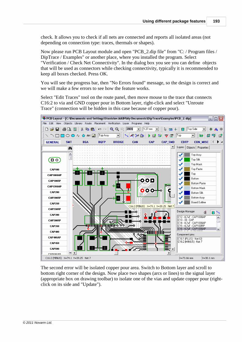
Using different package features 193
© 2011 Novarm Ltd.
check. It allows you to check if all nets are connected and reports all isolated areas (notdepending on connection type: traces, thermals or shapes).
Now please run PCB Layout module and open "PCB_2.dip file" from "C: / Program files /DipTrace / Examples" or another place, where you installed the program. Select"Verification / Check Net Connectivity". In the dialog box you see you can define objectsthat will be used as connectors while checking connectivity, typically it is recommended tokeep all boxes checked. Press OK.
You will see the progress bar, then "No Errors found" message, so the design is correct andwe will make a few errors to see how the feature works.
Select "Edit Traces" tool on the route panel, then move mouse to the trace that connectsC16:2 to via and GND copper pour in Bottom layer, right-click and select "UnrouteTrace" (connection will be hidden in this case because of copper pour).
The second error will be isolated copper pour area. Switch to Bottom layer and scroll tobottom right corner of the design. Now place two shapes (arcs or lines) to the signal layer(appropriate box on drawing toolbar) to isolate one of the vias and update copper pour (right-click on its side and "Update").
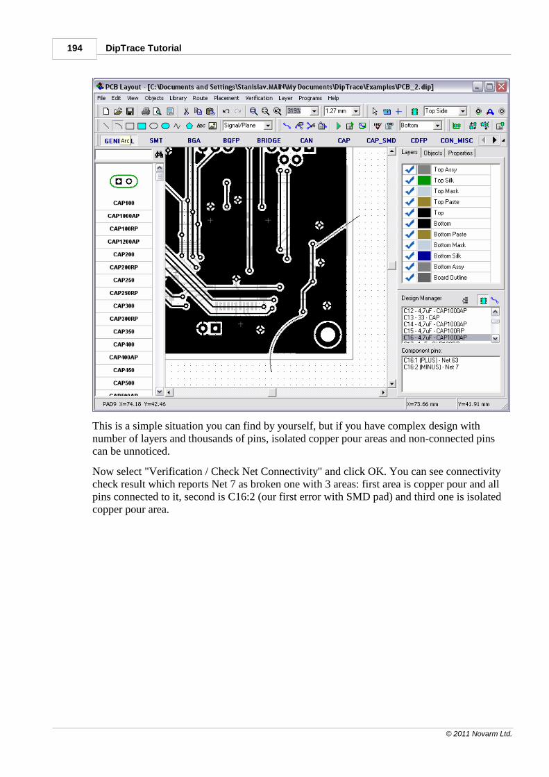
DipTrace Tutorial194
© 2011 Novarm Ltd.
This is a simple situation you can find by yourself, but if you have complex design withnumber of layers and thousands of pins, isolated copper pour areas and non-connected pinscan be unnoticed.
Now select "Verification / Check Net Connectivity" and click OK. You can see connectivitycheck result which reports Net 7 as broken one with 3 areas: first area is copper pour and allpins connected to it, second is C16:2 (our first error with SMD pad) and third one is isolatedcopper pour area.
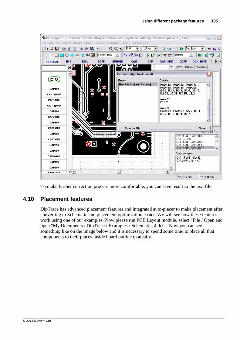
Using different package features 195
© 2011 Novarm Ltd.
To make further correction process more comfortable, you can save result to the text file.
4.10 Placement features
DipTrace has advanced placement features and integrated auto-placer to make placement afterconverting to Schematic and placement optimization easier. We will see how these featureswork using one of our examples. Now please run PCB Layout module, select "File / Open andopen "My Documents / DipTrace / Examples / Schematic_4.dch". Now you can seesomething like on the image below and it is necessary to spend some time to place all thatcomponents to their places inside board outline manually.
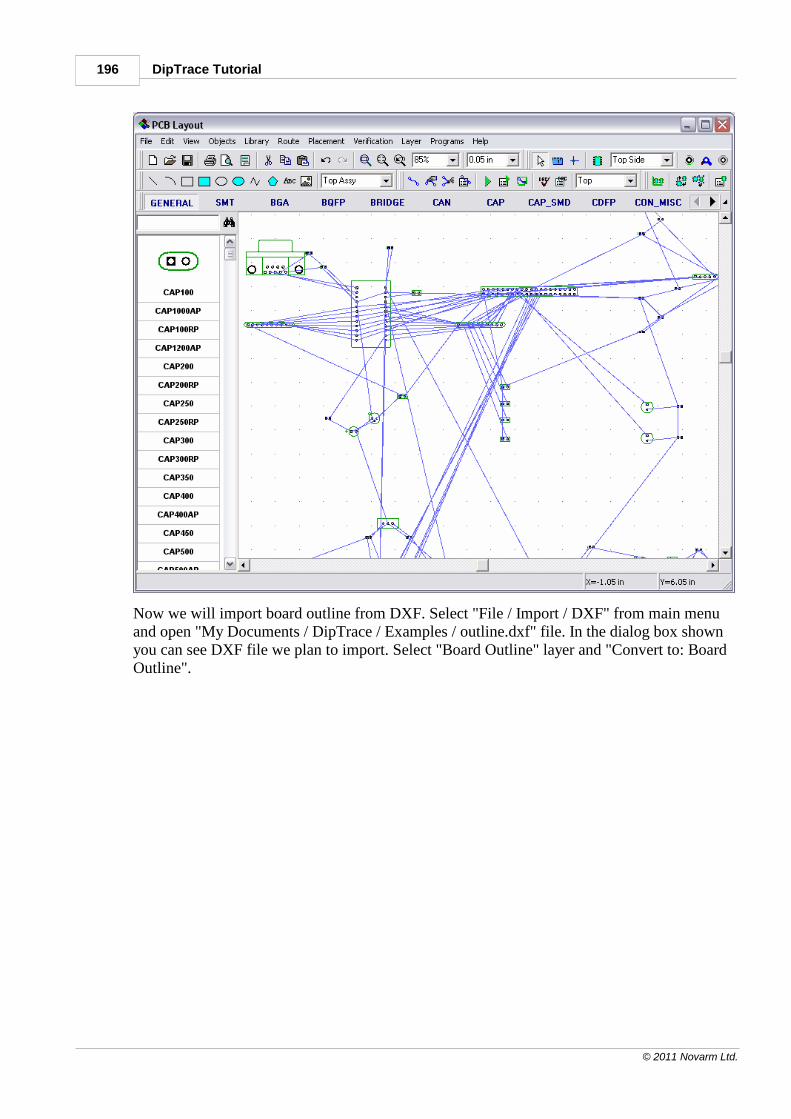
DipTrace Tutorial196
© 2011 Novarm Ltd.
Now we will import board outline from DXF. Select "File / Import / DXF" from main menuand open "My Documents / DipTrace / Examples / outline.dxf" file. In the dialog box shownyou can see DXF file we plan to import. Select "Board Outline" layer and "Convert to: BoardOutline".
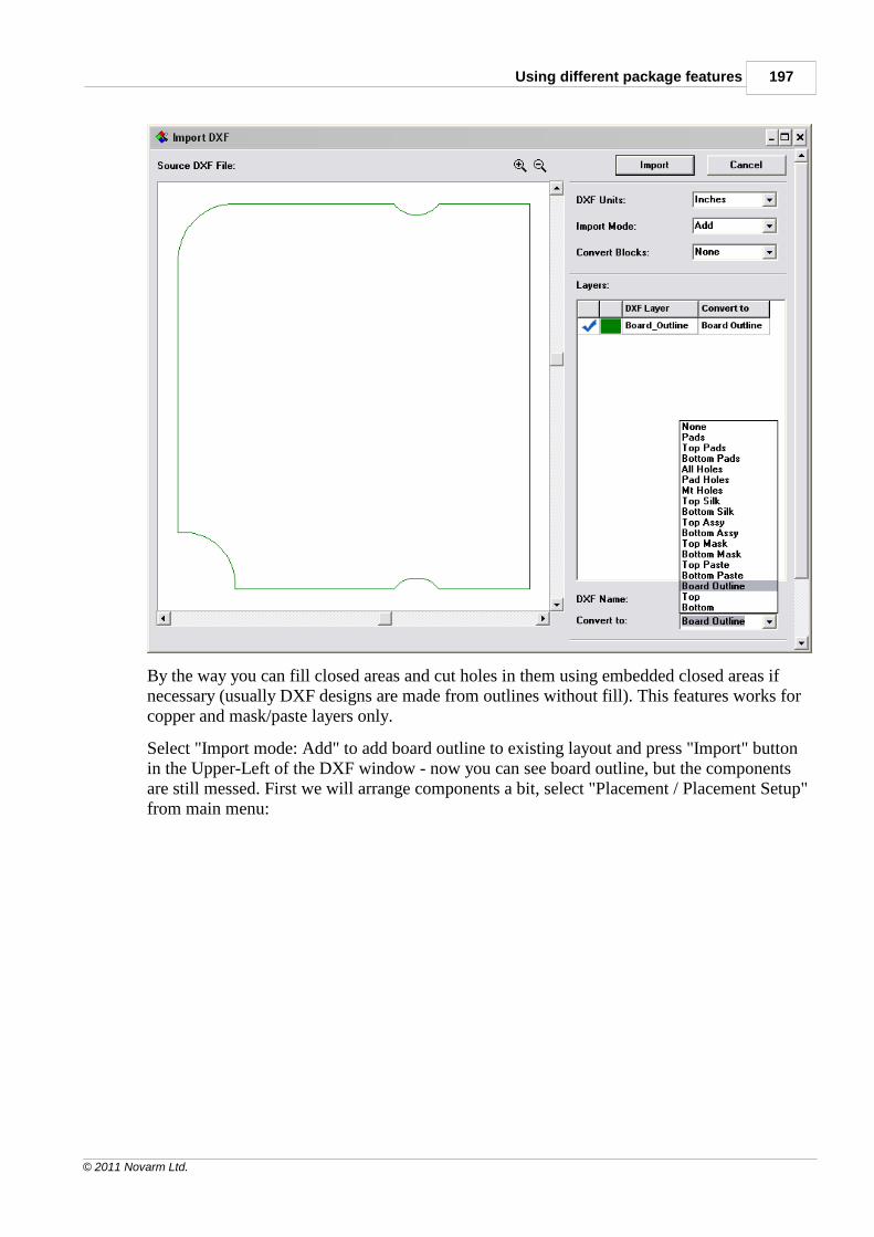
Using different package features 197
© 2011 Novarm Ltd.
By the way you can fill closed areas and cut holes in them using embedded closed areas ifnecessary (usually DXF designs are made from outlines without fill). This features works forcopper and mask/paste layers only.
Select "Import mode: Add" to add board outline to existing layout and press "Import" buttonin the Upper-Left of the DXF window - now you can see board outline, but the componentsare still messed. First we will arrange components a bit, select "Placement / Placement Setup"from main menu:
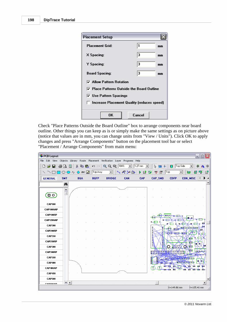
DipTrace Tutorial198
© 2011 Novarm Ltd.
Check "Place Patterns Outside the Board Outline" box to arrange components near boardoutline. Other things you can keep as is or simply make the same settings as on picture above(notice that values are in mm, you can change units from "View / Units"). Click OK to applychanges and press "Arrange Components" button on the placement tool bar or select"Placement / Arrange Components" from main menu:
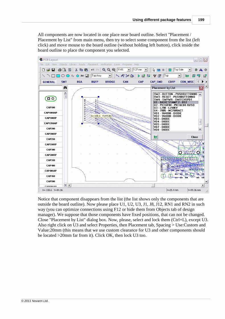
Using different package features 199
© 2011 Novarm Ltd.
All components are now located in one place near board outline. Select "Placement /Placement by List" from main menu, then try to select some component from the list (leftclick) and move mouse to the board outline (without holding left button), click inside theboard outline to place the component you selected.
Notice that component disappears from the list (the list shows only the components that areoutside the board outline). Now please place U1, U2, U3, J1, J8, J12, RN1 and RN2 in suchway (you can optimize connections using F12 or hide them from Objects tab of designmanager). We suppose that those components have fixed positions, that can not be changed.Close "Placement by List" dialog box. Now, please, select and lock them (Ctrl+L), except U3.Also right click on U3 and select Properties, then Placement tab, Spacing > Use:Custom andValue:20mm (this means that we use custom clearance for U3 and other components shouldbe located >20mm far from it). Click OK, then lock U3 too.
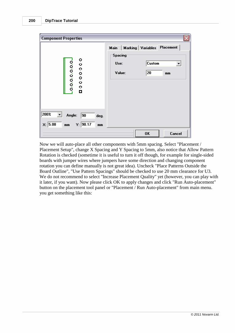
DipTrace Tutorial200
© 2011 Novarm Ltd.
Now we will auto-place all other components with 5mm spacing. Select "Placement /Placement Setup", change X Spacing and Y Spacing to 5mm, also notice that Allow PatternRotation is checked (sometime it is useful to turn it off though, for example for single-sidedboards with jumper wires where jumpers have some direction and changing componentrotation you can define manually is not great idea). Uncheck "Place Patterns Outside theBoard Outline", "Use Pattern Spacings" should be checked to use 20 mm clearance for U3.We do not recommend to select "Increase Placement Quality" yet (however, you can play withit later, if you want). Now please click OK to apply changes and click "Run Auto-placement"button on the placement tool panel or "Placement / Run Auto-placement" from main menu.you get something like this:
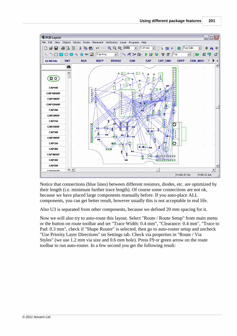
Using different package features 201
© 2011 Novarm Ltd.
Notice that connections (blue lines) between different resistors, diodes, etc. are optimized bytheir length (i.e. minimum further trace length). Of course some connections are not ok,because we have placed large components manually before. If you auto-place ALLcomponents, you can get better result, however usually this is not acceptable in real life.
Also U3 is separated from other components, because we defined 20 mm spacing for it.
Now we will also try to auto-route this layout. Select "Route / Route Setup" from main menuor the button on route toolbar and set "Trace Width: 0.4 mm", "Clearance: 0.4 mm", "Trace toPad: 0.3 mm", check if "Shape Router" is selected, then go to auto-router setup and uncheck"Use Priority Layer Directions" on Settings tab. Check via properties in "Route / ViaStyles" (we use 1.2 mm via size and 0.6 mm hole). Press F9 or green arrow on the routetoolbar to run auto-router. In a few second you get the following result:
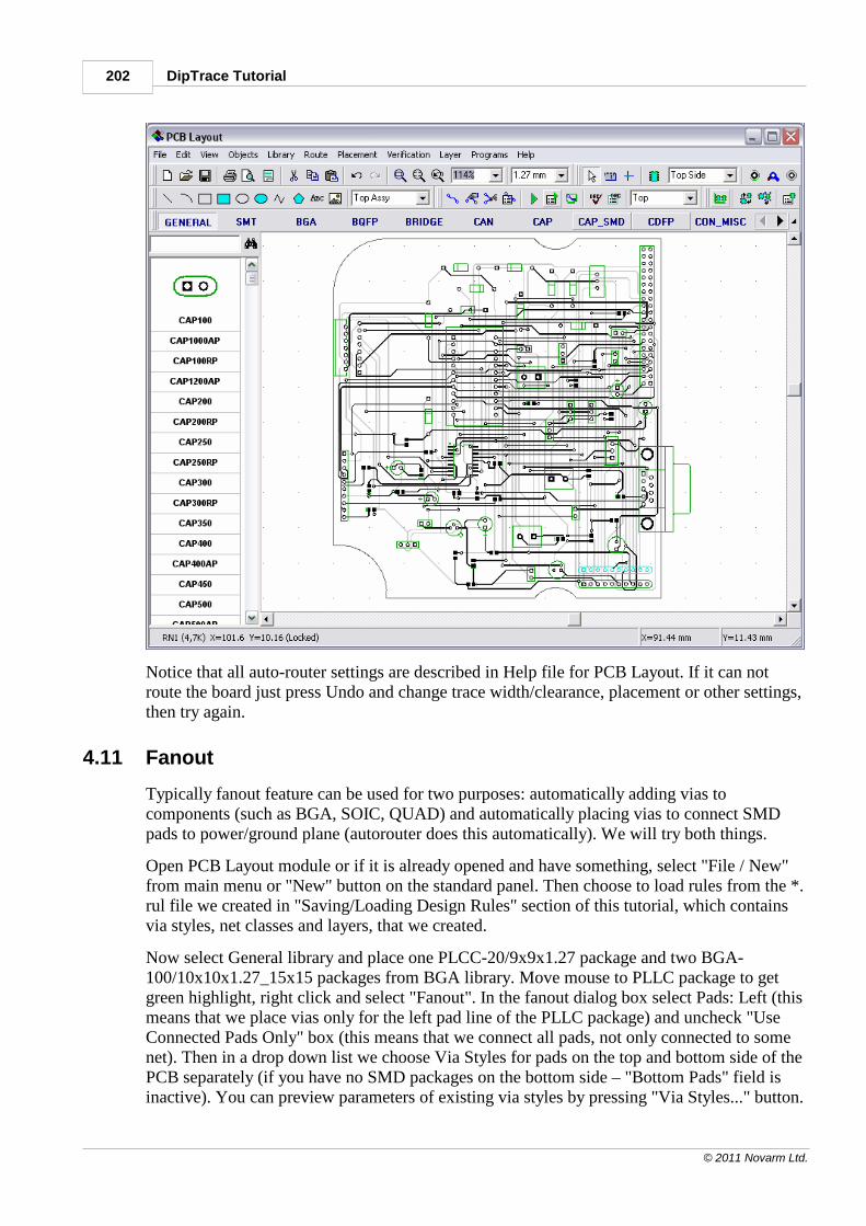
DipTrace Tutorial202
© 2011 Novarm Ltd.
Notice that all auto-router settings are described in Help file for PCB Layout. If it can notroute the board just press Undo and change trace width/clearance, placement or other settings,then try again.
4.11 Fanout
Typically fanout feature can be used for two purposes: automatically adding vias tocomponents (such as BGA, SOIC, QUAD) and automatically placing vias to connect SMDpads to power/ground plane (autorouter does this automatically). We will try both things.
Open PCB Layout module or if it is already opened and have something, select "File / New"from main menu or "New" button on the standard panel. Then choose to load rules from the *.rul file we created in "Saving/Loading Design Rules" section of this tutorial, which containsvia styles, net classes and layers, that we created.
Now select General library and place one PLCC-20/9x9x1.27 package and two BGA-100/10x10x1.27_15x15 packages from BGA library. Move mouse to PLLC package to getgreen highlight, right click and select "Fanout". In the fanout dialog box select Pads: Left (thismeans that we place vias only for the left pad line of the PLLC package) and uncheck "UseConnected Pads Only" box (this means that we connect all pads, not only connected to somenet). Then in a drop down list we choose Via Styles for pads on the top and bottom side of thePCB separately (if you have no SMD packages on the bottom side – "Bottom Pads" field isinactive). You can preview parameters of existing via styles by pressing "Via Styles..." button.
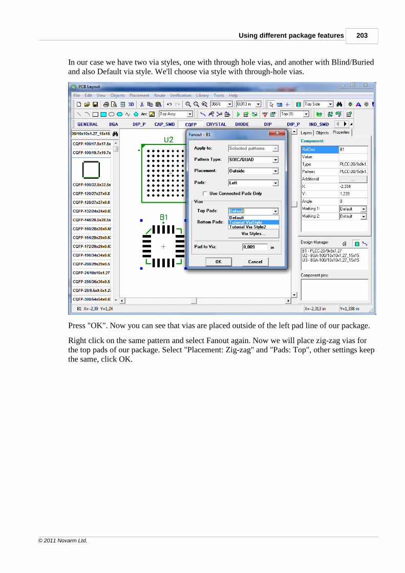
Using different package features 203
© 2011 Novarm Ltd.
In our case we have two via styles, one with through hole vias, and another with Blind/Buriedand also Default via style. We'll choose via style with through-hole vias.
Press "OK". Now you can see that vias are placed outside of the left pad line of our package.
Right click on the same pattern and select Fanout again. Now we will place zig-zag vias forthe top pads of our package. Select "Placement: Zig-zag" and "Pads: Top", other settings keepthe same, click OK.
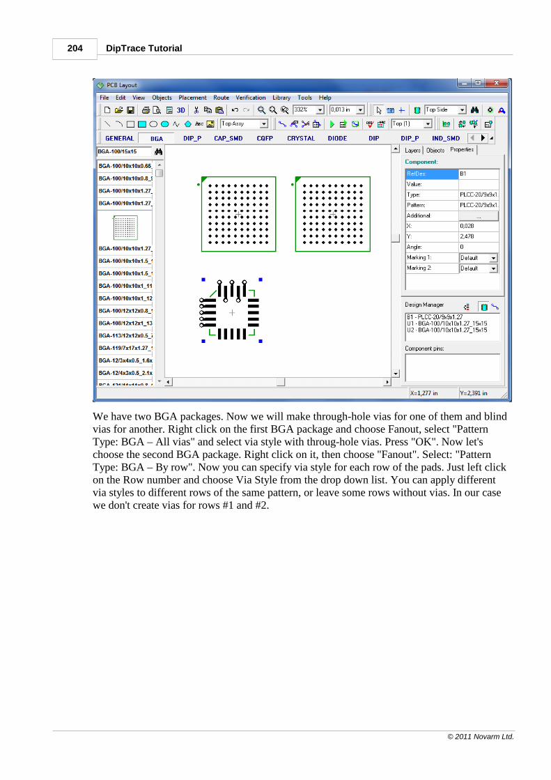
DipTrace Tutorial204
© 2011 Novarm Ltd.
We have two BGA packages. Now we will make through-hole vias for one of them and blindvias for another. Right click on the first BGA package and choose Fanout, select "PatternType: BGA – All vias" and select via style with throug-hole vias. Press "OK". Now let'schoose the second BGA package. Right click on it, then choose "Fanout". Select: "PatternType: BGA – By row". Now you can specify via style for each row of the pads. Just left clickon the Row number and choose Via Style from the drop down list. You can apply differentvia styles to different rows of the same pattern, or leave some rows without vias. In our casewe don't create vias for rows #1 and #2.
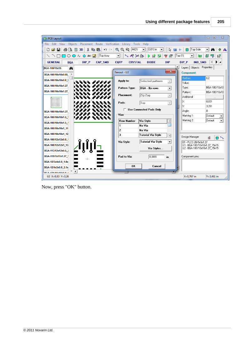
Using different package features 205
© 2011 Novarm Ltd.
Now, press "OK" button.
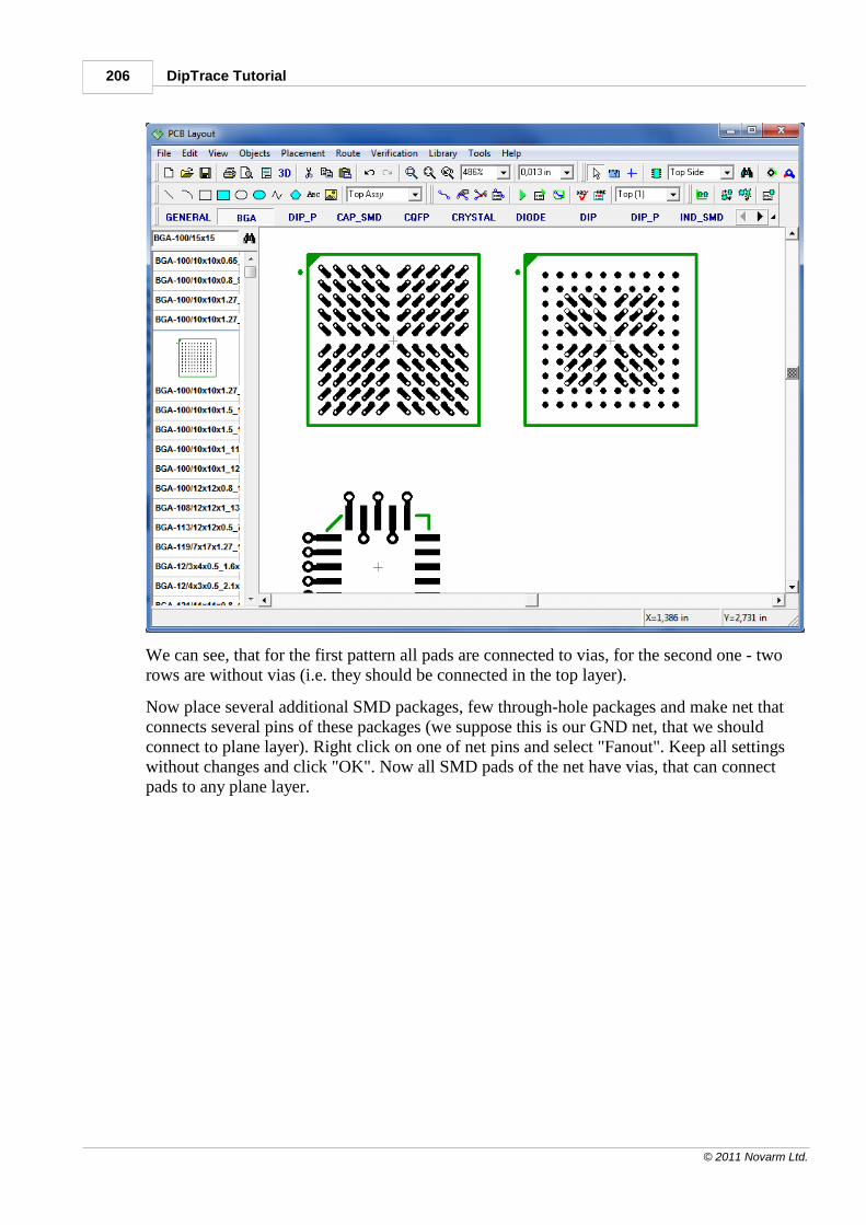
DipTrace Tutorial206
© 2011 Novarm Ltd.
We can see, that for the first pattern all pads are connected to vias, for the second one - tworows are without vias (i.e. they should be connected in the top layer).
Now place several additional SMD packages, few through-hole packages and make net thatconnects several pins of these packages (we suppose this is our GND net, that we shouldconnect to plane layer). Right click on one of net pins and select "Fanout". Keep all settingswithout changes and click "OK". Now all SMD pads of the net have vias, that can connectpads to any plane layer.
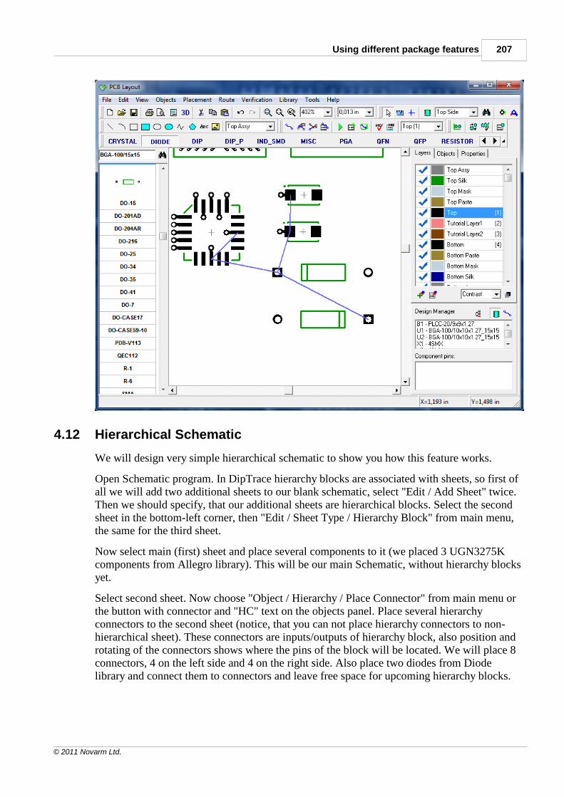
Using different package features 207
© 2011 Novarm Ltd.
4.12 Hierarchical Schematic
We will design very simple hierarchical schematic to show you how this feature works.
Open Schematic program. In DipTrace hierarchy blocks are associated with sheets, so first ofall we will add two additional sheets to our blank schematic, select "Edit / Add Sheet" twice.Then we should specify, that our additional sheets are hierarchical blocks. Select the secondsheet in the bottom-left corner, then "Edit / Sheet Type / Hierarchy Block" from main menu,the same for the third sheet.
Now select main (first) sheet and place several components to it (we placed 3 UGN3275Kcomponents from Allegro library). This will be our main Schematic, without hierarchy blocksyet.
Select second sheet. Now choose "Object / Hierarchy / Place Connector" from main menu orthe button with connector and "HC" text on the objects panel. Place several hierarchyconnectors to the second sheet (notice, that you can not place hierarchy connectors to non-hierarchical sheet). These connectors are inputs/outputs of hierarchy block, also position androtating of the connectors shows where the pins of the block will be located. We will place 8connectors, 4 on the left side and 4 on the right side. Also place two diodes from Diodelibrary and connect them to connectors and leave free space for upcoming hierarchy blocks.
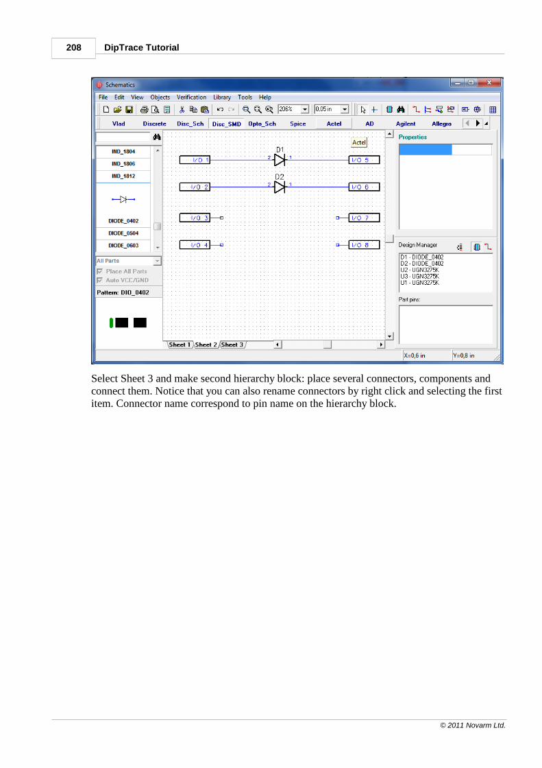
DipTrace Tutorial208
© 2011 Novarm Ltd.
Select Sheet 3 and make second hierarchy block: place several connectors, components andconnect them. Notice that you can also rename connectors by right click and selecting the firstitem. Connector name correspond to pin name on the hierarchy block.
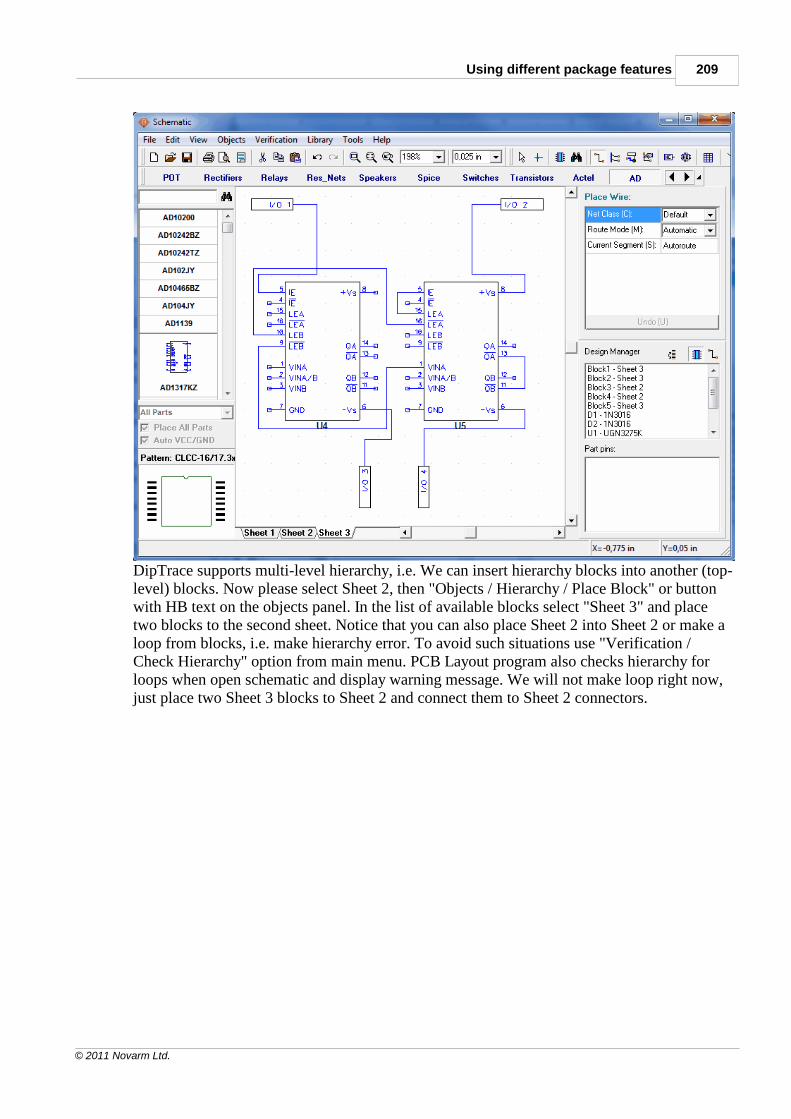
Using different package features 209
© 2011 Novarm Ltd.
DipTrace supports multi-level hierarchy, i.e. We can insert hierarchy blocks into another (top-level) blocks. Now please select Sheet 2, then "Objects / Hierarchy / Place Block" or buttonwith HB text on the objects panel. In the list of available blocks select "Sheet 3" and placetwo blocks to the second sheet. Notice that you can also place Sheet 2 into Sheet 2 or make aloop from blocks, i.e. make hierarchy error. To avoid such situations use "Verification /Check Hierarchy" option from main menu. PCB Layout program also checks hierarchy forloops when open schematic and display warning message. We will not make loop right now,just place two Sheet 3 blocks to Sheet 2 and connect them to Sheet 2 connectors.
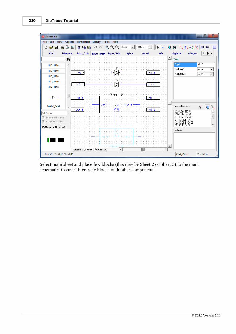
DipTrace Tutorial210
© 2011 Novarm Ltd.
Select main sheet and place few blocks (this may be Sheet 2 or Sheet 3) to the mainschematic. Connect hierarchy blocks with other components.
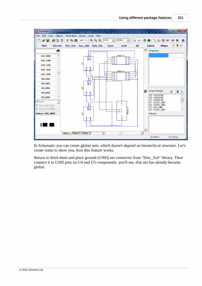
Using different package features 211
© 2011 Novarm Ltd.
In Schematic you can create global nets, which doesn't depend on hierarchical structure. Let'screate some to show you, how this feature works.
Return to third sheet and place ground (GND) net connector from "Disc_Sch" library. Thenconnect it to GND pins on U4 and U5 components. you'll see, that net has already becameglobal.
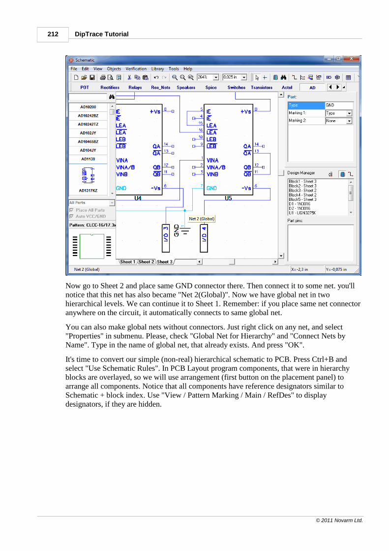
DipTrace Tutorial212
© 2011 Novarm Ltd.
Now go to Sheet 2 and place same GND connector there. Then connect it to some net. you'llnotice that this net has also became "Net 2(Global)". Now we have global net in twohierarchical levels. We can continue it to Sheet 1. Remember: if you place same net connectoranywhere on the circuit, it automatically connects to same global net.
You can also make global nets without connectors. Just right click on any net, and select"Properties" in submenu. Please, check "Global Net for Hierarchy" and "Connect Nets byName". Type in the name of global net, that already exists. And press "OK".
It's time to convert our simple (non-real) hierarchical schematic to PCB. Press Ctrl+B andselect "Use Schematic Rules". In PCB Layout program components, that were in hierarchyblocks are overlayed, so we will use arrangement (first button on the placement panel) toarrange all components. Notice that all components have reference designators similar toSchematic + block index. Use "View / Pattern Marking / Main / RefDes" to displaydesignators, if they are hidden.
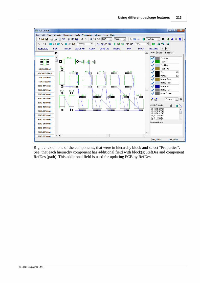
Using different package features 213
© 2011 Novarm Ltd.
Right click on one of the components, that were in hierarchy block and select “Properties”.See, that each hierarchy component has additional field with block(s) RefDes and componentRefDes (path). This additional field is used for updating PCB by RefDes.
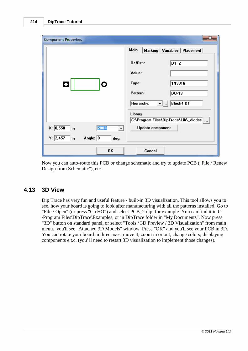
DipTrace Tutorial214
© 2011 Novarm Ltd.
Now you can auto-route this PCB or change schematic and try to update PCB ("File / RenewDesign from Schematic"), etc.
4.13 3D View
Dip Trace has very fun and useful feature - built-in 3D visualization. This tool allows you tosee, how your board is going to look after manufacturing with all the patterns installed. Go to"File / Open" (or press "Ctrl+O") and select PCB_2.dip, for example. You can find it in C:\Program Files\DipTrace\Examples, or in DipTrace folder in "My Documents". Now press"3D" button on standard panel, or select "Tools / 3D Preview / 3D Visualization" from mainmenu. you'll see "Attached 3D Models" window. Press "OK" and you'll see your PCB in 3D.You can rotate your board in three axes, move it, zoom in or out, change colors, displayingcomponents e.t.c. (you' ll need to restart 3D visualization to implement those changes).
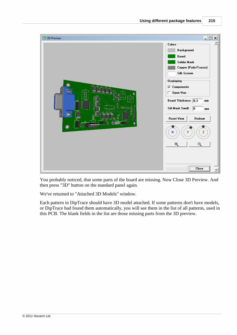
Using different package features 215
© 2011 Novarm Ltd.
You probably noticed, that some parts of the board are missing. Now Close 3D Preview. Andthen press "3D" button on the standard panel again.
We've returned to "Attached 3D Models" window.
Each pattern in DipTrace should have 3D model attached. If some patterns don't have models,or DipTrace had found them automatically, you will see them in the list of all patterns, used inthis PCB. The blank fields in the list are those missing parts from the 3D preview.
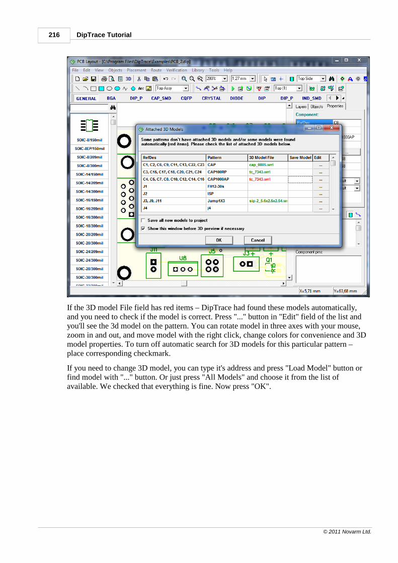
DipTrace Tutorial216
© 2011 Novarm Ltd.
If the 3D model File field has red items – DipTrace had found these models automatically,and you need to check if the model is correct. Press "..." button in "Edit" field of the list andyou'll see the 3d model on the pattern. You can rotate model in three axes with your mouse,zoom in and out, and move model with the right click, change colors for convenience and 3Dmodel properties. To turn off automatic search for 3D models for this particular pattern –place corresponding checkmark.
If you need to change 3D model, you can type it's address and press "Load Model" button orfind model with "..." button. Or just press "All Models" and choose it from the list ofavailable. We checked that everything is fine. Now press "OK".
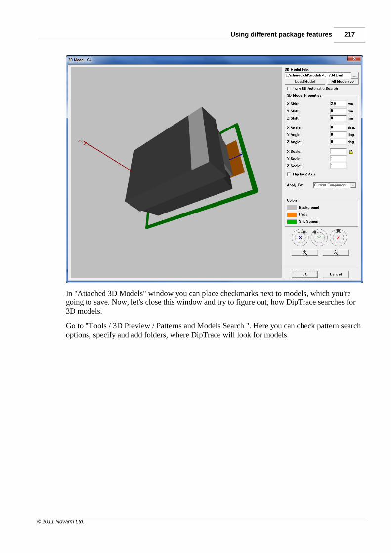
Using different package features 217
© 2011 Novarm Ltd.
In "Attached 3D Models" window you can place checkmarks next to models, which you'regoing to save. Now, let's close this window and try to figure out, how DipTrace searches for3D models.
Go to "Tools / 3D Preview / Patterns and Models Search ". Here you can check pattern searchoptions, specify and add folders, where DipTrace will look for models.
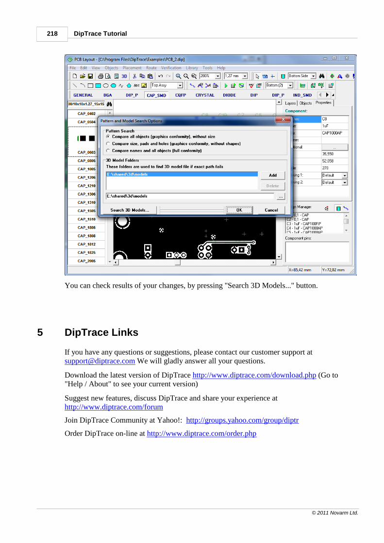
DipTrace Tutorial218
© 2011 Novarm Ltd.
You can check results of your changes, by pressing "Search 3D Models..." button.
5 DipTrace Links
If you have any questions or suggestions, please contact our customer support at [email protected] We will gladly answer all your questions.
Download the latest version of DipTrace http://www.diptrace.com/download.php (Go to"Help / About" to see your current version)
Suggest new features, discuss DipTrace and share your experience at http://www.diptrace.com/forum
Join DipTrace Community at Yahoo!: http://groups.yahoo.com/group/diptr
Order DipTrace on-line at http://www.diptrace.com/order.php
Related Documents


