Tutorial 6 Derek Wright Wednesday, March 2 nd , 2005

Tutorial 6 Derek Wright Wednesday, March 2 nd, 2005.
Dec 27, 2015
Welcome message from author
This document is posted to help you gain knowledge. Please leave a comment to let me know what you think about it! Share it to your friends and learn new things together.
Transcript

Tutorial 6
Derek Wright
Wednesday, March 2nd, 2005
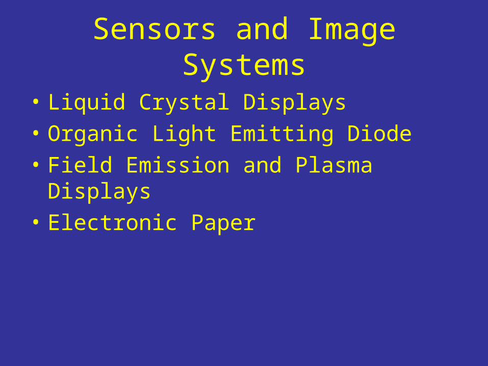
Sensors and Image Systems
• Liquid Crystal Displays
• Organic Light Emitting Diode
• Field Emission and Plasma Displays
• Electronic Paper
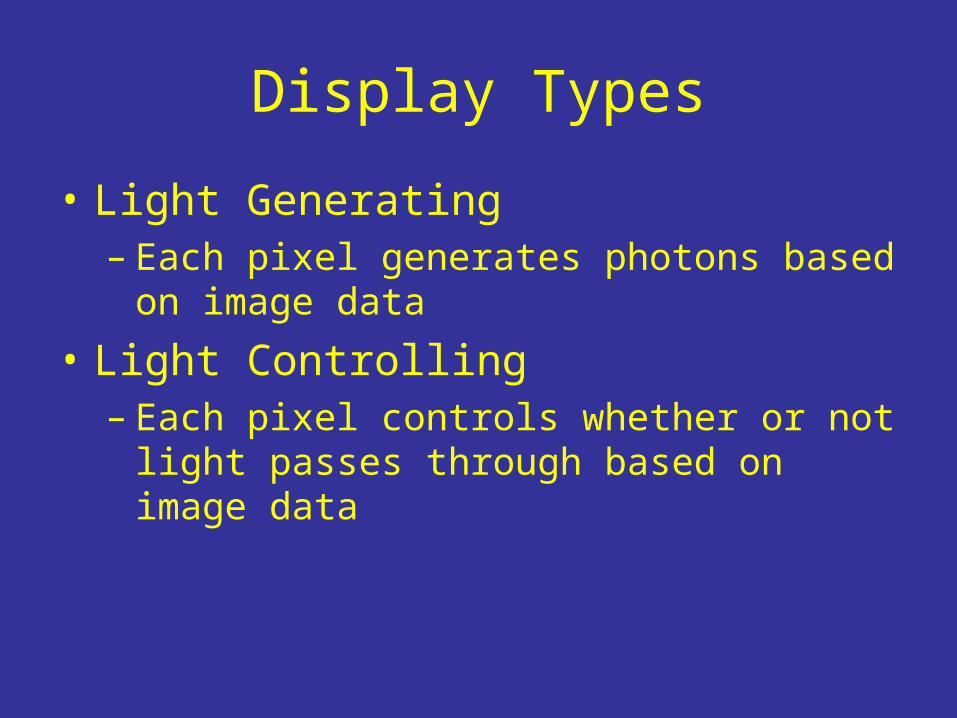
Display Types
• Light Generating– Each pixel generates photons based on
image data
• Light Controlling– Each pixel controls whether or not light
passes through based on image data
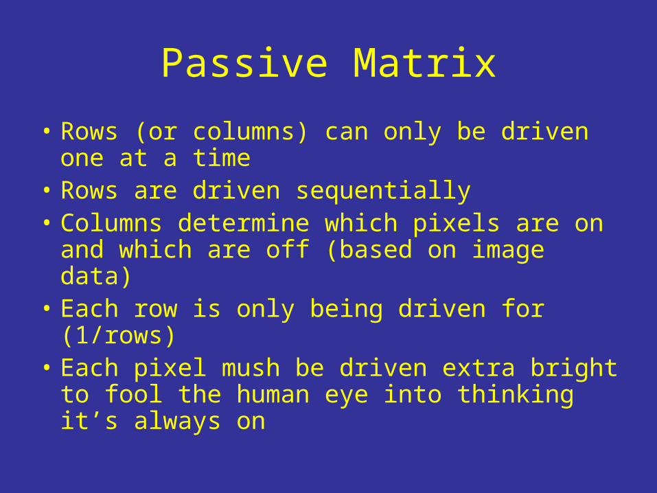
Passive Matrix
• Rows (or columns) can only be driven one at a time
• Rows are driven sequentially• Columns determine which pixels are on
and which are off (based on image data)• Each row is only being driven for (1/rows)• Each pixel mush be driven extra bright to
fool the human eye into thinking it’s always on
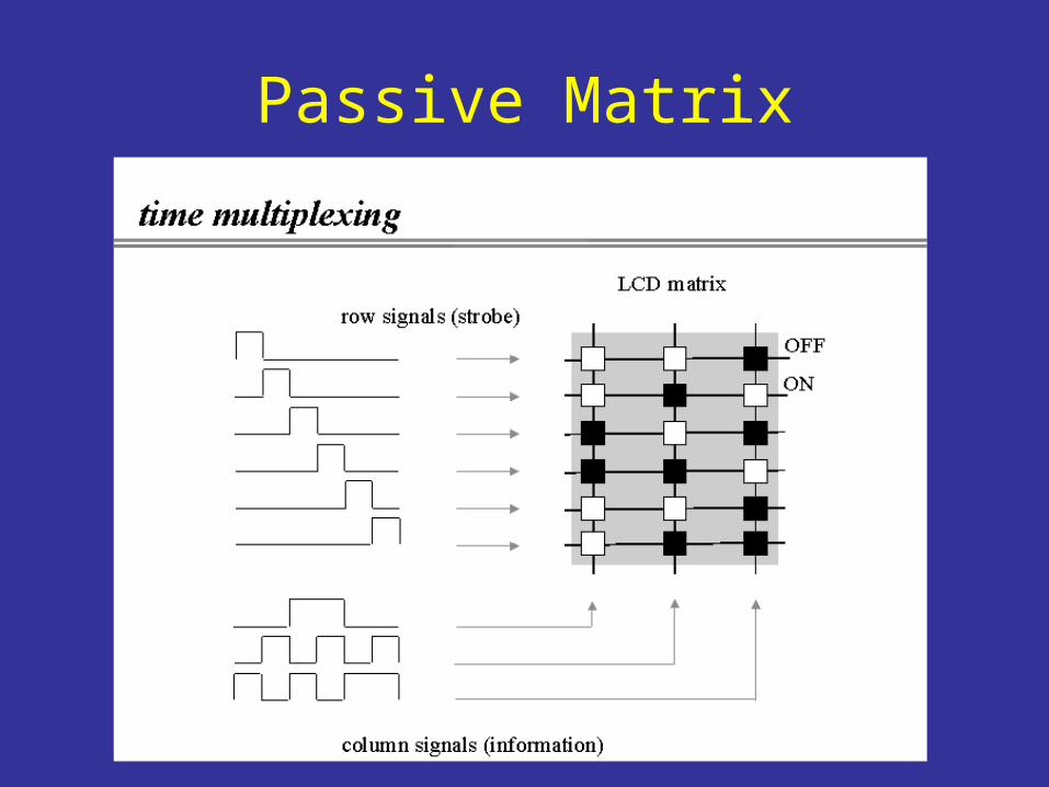
Passive Matrix
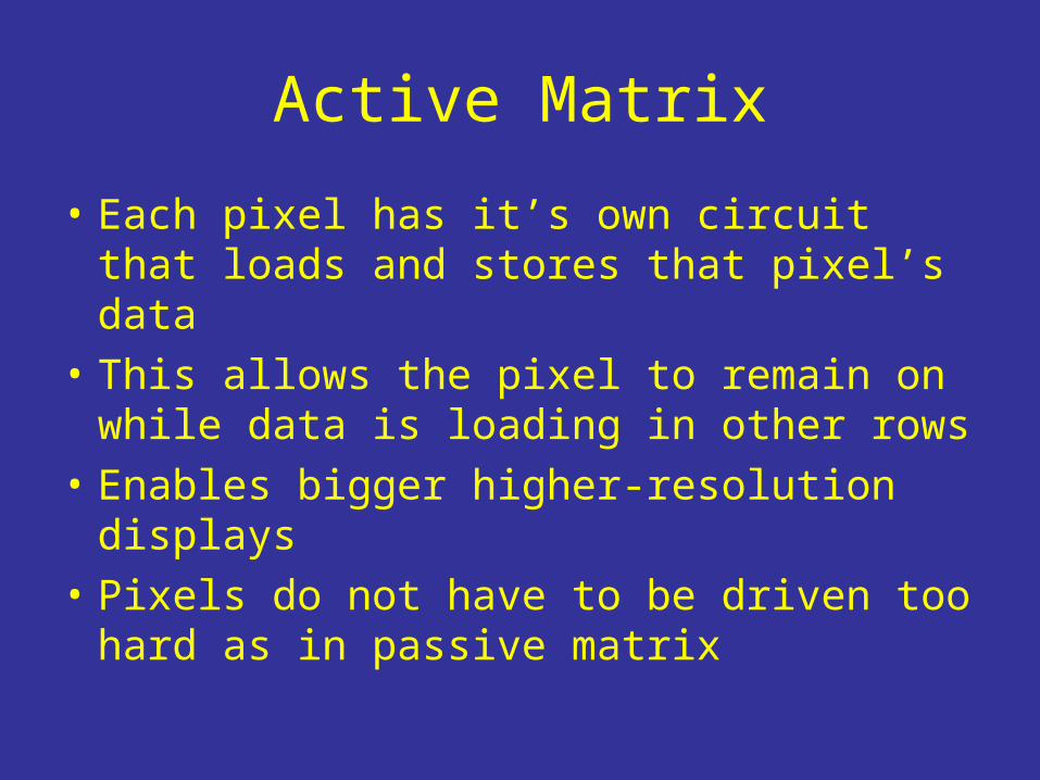
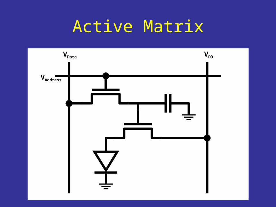
Active Matrix
• Each pixel has it’s own circuit that loads and stores that pixel’s data
• This allows the pixel to remain on while data is loading in other rows
• Enables bigger higher-resolution displays
• Pixels do not have to be driven too hard as in passive matrix
Active Matrix
VDDVData
VAddress
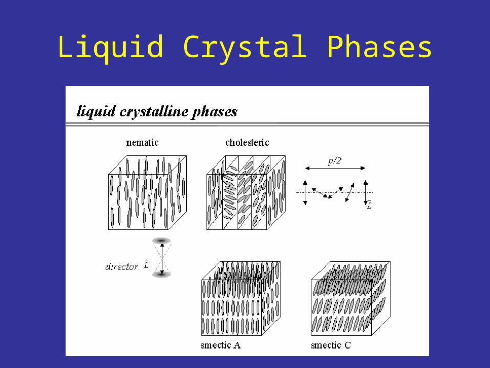
Liquid Crystal Phases
Liquid Crystal Displays
• Liquid Crystal Displays (LCDs) exploit liquid crystal’s ability to bend light
• Polarized light enters the back of a liquid crystal pixel
• The light passes through nematic phase liquid crystal, which bends the light’s polarization plane
• The light passes through another polarizer (NW)• When an E-field is applied, the liquid crystal
doesn’t bend the light and it can’t pass through the polarizer (NW)
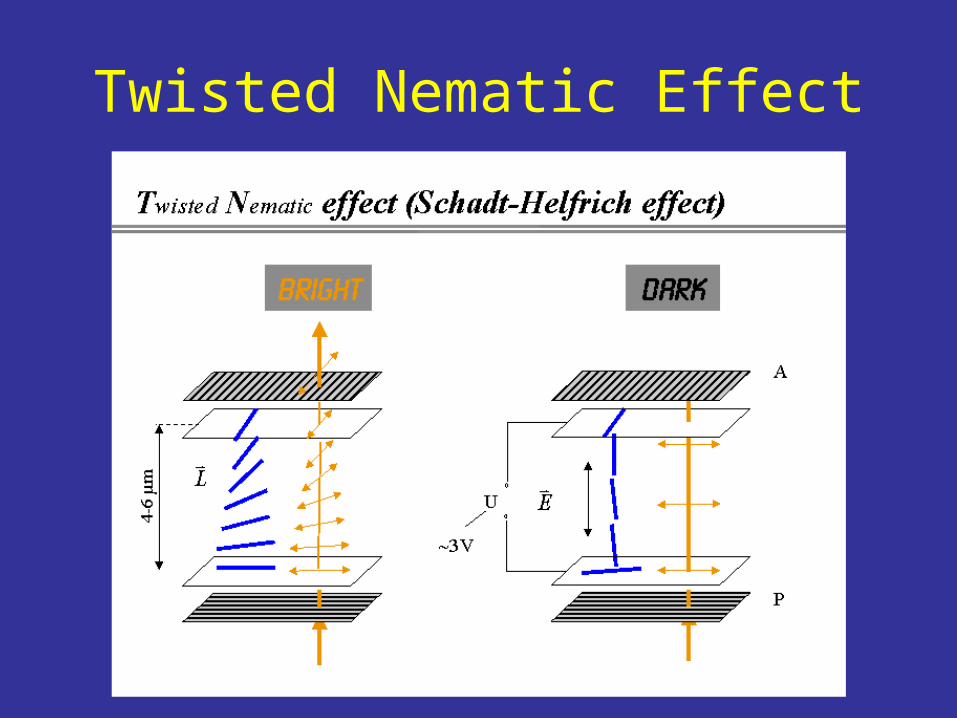
Twisted Nematic Effect
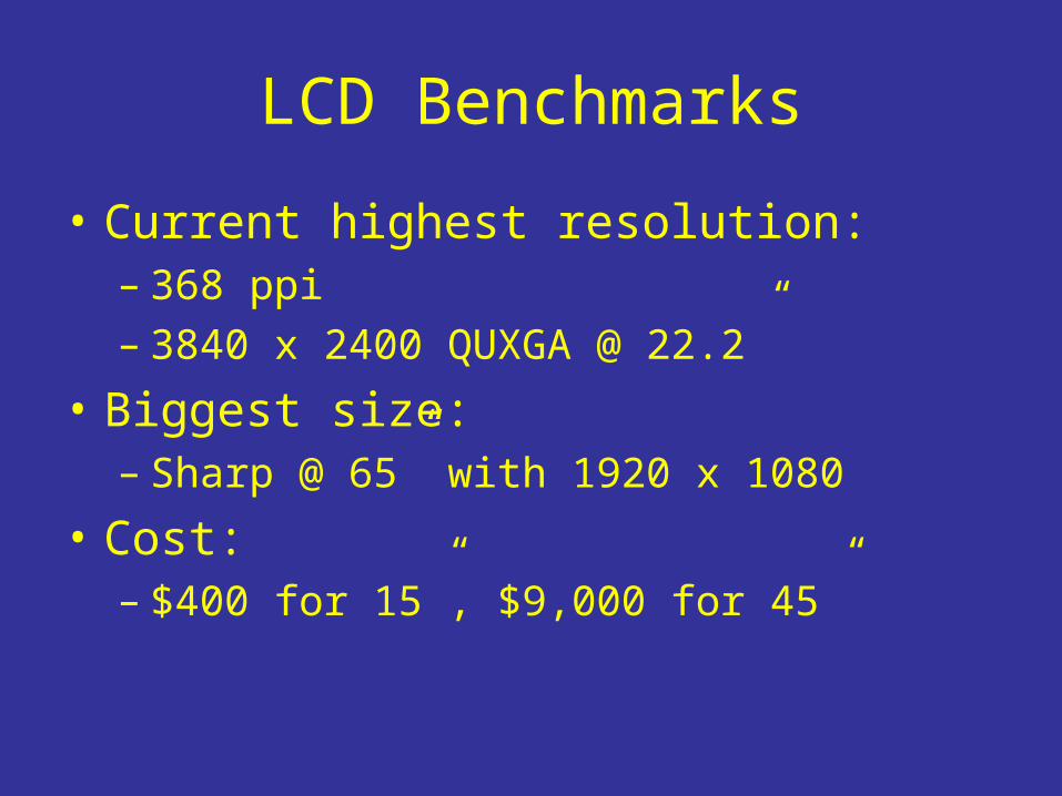
LCD Benchmarks
• Current highest resolution:– 368 ppi– 3840 x 2400 QUXGA @ 22.2”
• Biggest size:– Sharp @ 65” with 1920 x 1080
• Cost:– $400 for 15”, $9,000 for 45”
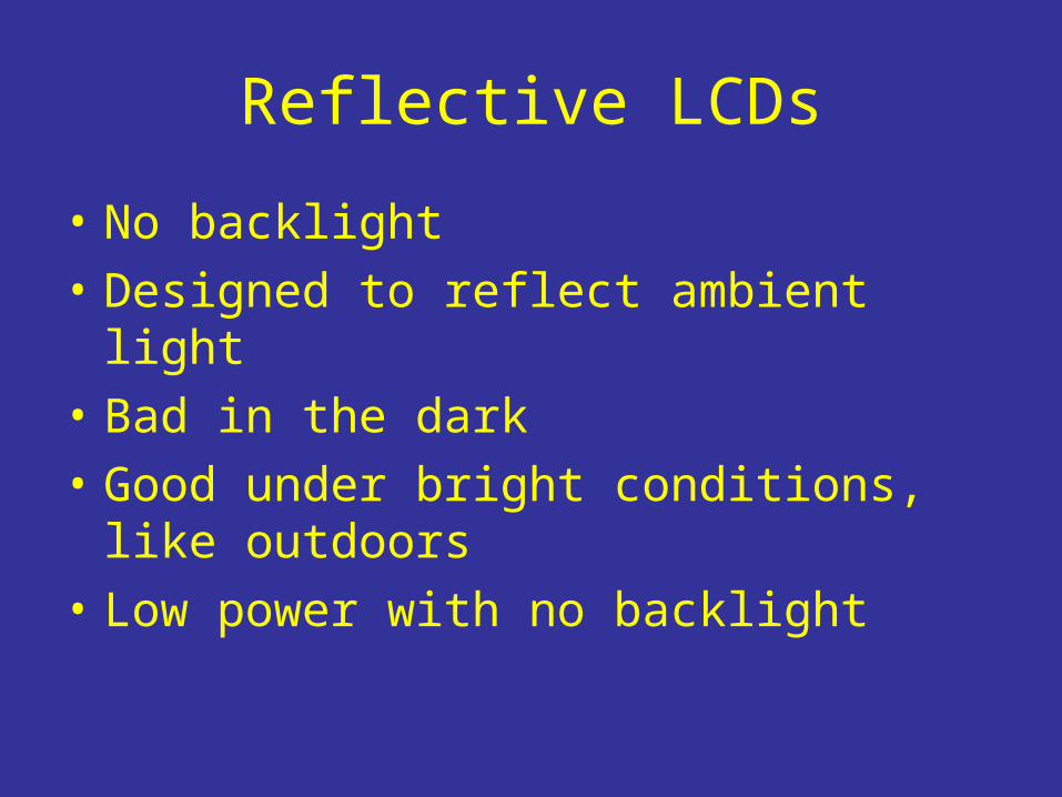
Reflective LCDs
• No backlight
• Designed to reflect ambient light
• Bad in the dark
• Good under bright conditions, like outdoors
• Low power with no backlight
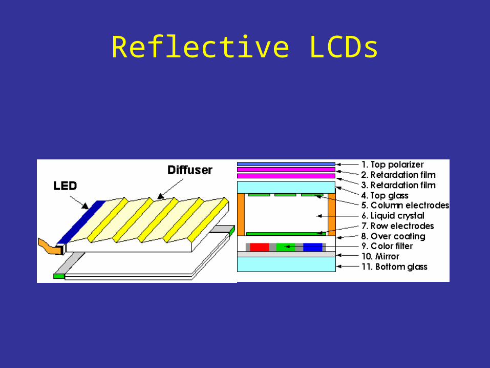
Reflective LCDs
Transreflective LCDs
• Combine features of both transmissive and reflective LCDs
• Reflective for high ambient lighting
• Transmissive for low ambient lighting
• Less power than a fully transmissive LCD
• Each pixel is divided into a reflective part and a transmissive part
Projection Displays
• An image is produced using either transmissive or reflective means
• Optical mirrors and lenses magnify the image to occupy a large area
• Liquid Crystal on Semiconductor (LCoS) current leader in projection televisions
• CMOS process means cheap and on-chip integration
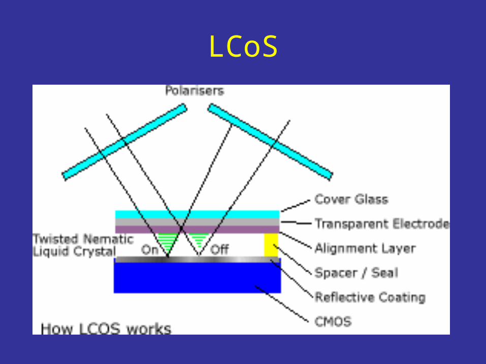
LCoS
OLEDs
• Organic Light Emitting Diodes
• Organic molecules can be tailored to act as an LED
• They can emit photons
• Brighter than current TVs
• Fast switching
• Should eventually be cheap
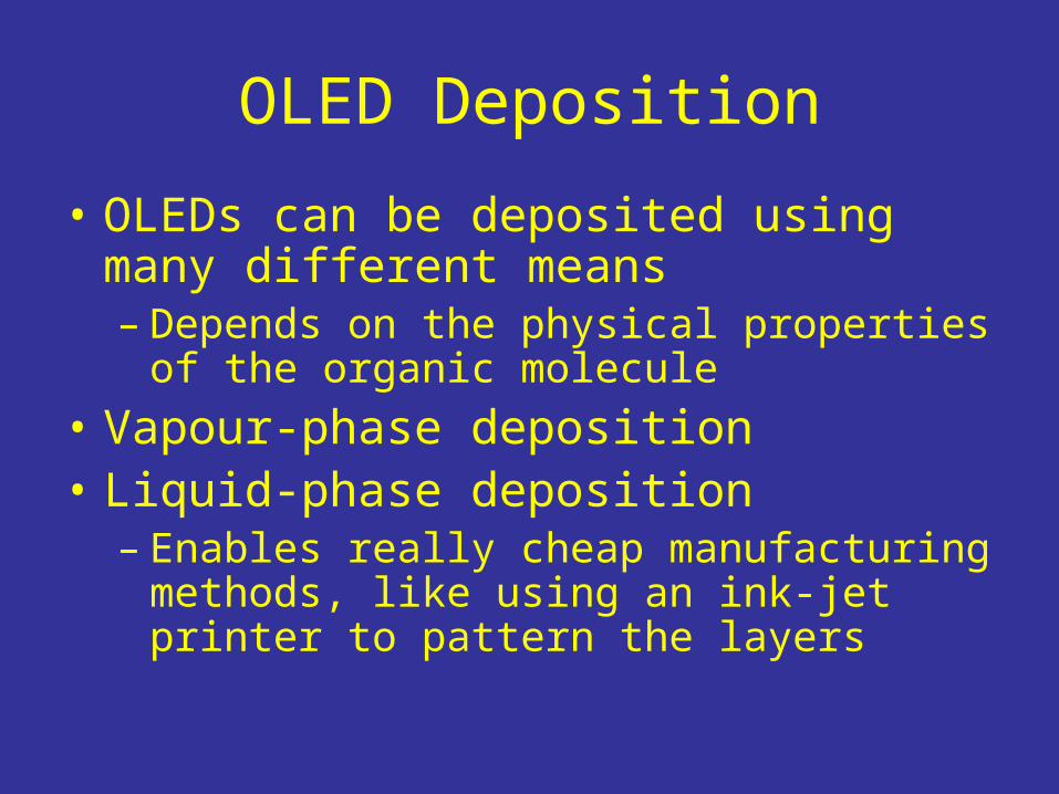
OLED Deposition
• OLEDs can be deposited using many different means– Depends on the physical properties of the
organic molecule
• Vapour-phase deposition• Liquid-phase deposition
– Enables really cheap manufacturing methods, like using an ink-jet printer to pattern the layers
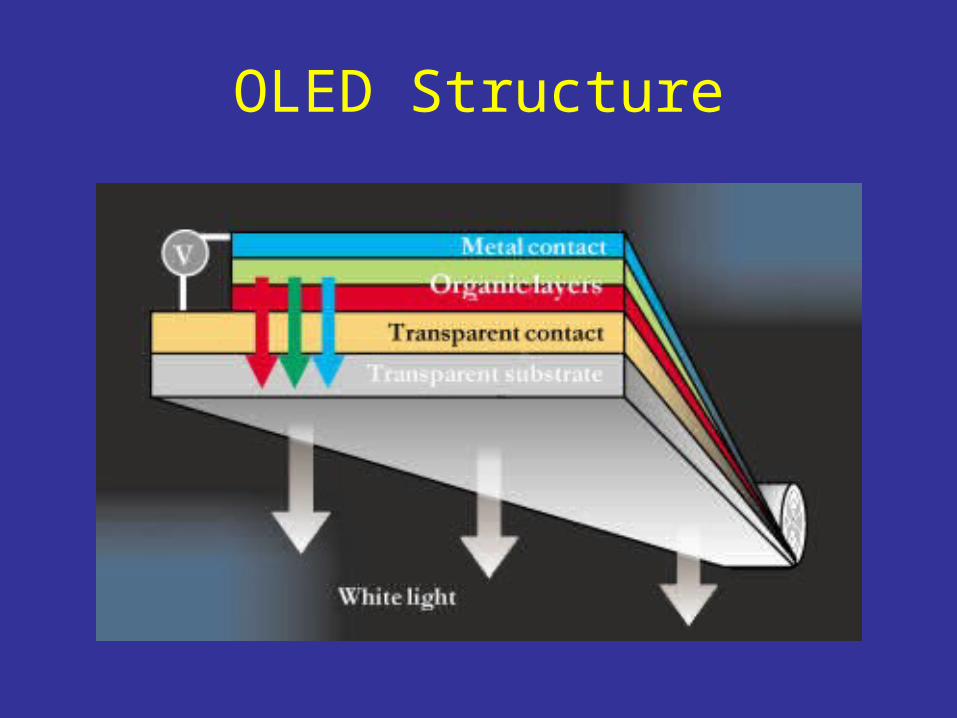
OLED Structure
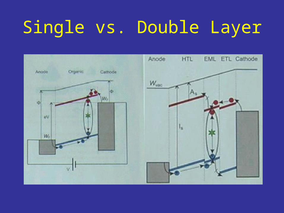
Single vs. Double Layer
Field Emission
• Occurs under high voltage
• Electrons are stripped off of an electron emitter
• Accelerated using externally applied E-field
• Sharp tips release more electrons
• Different than tunneling current
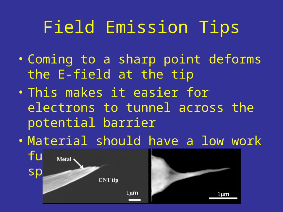
• Coming to a sharp point deforms the E-field at the tip
• This makes it easier for electrons to tunnel across the potential barrier
• Material should have a low work function and be resistant to sputtering
Field Emission Tips
Potential Barrier
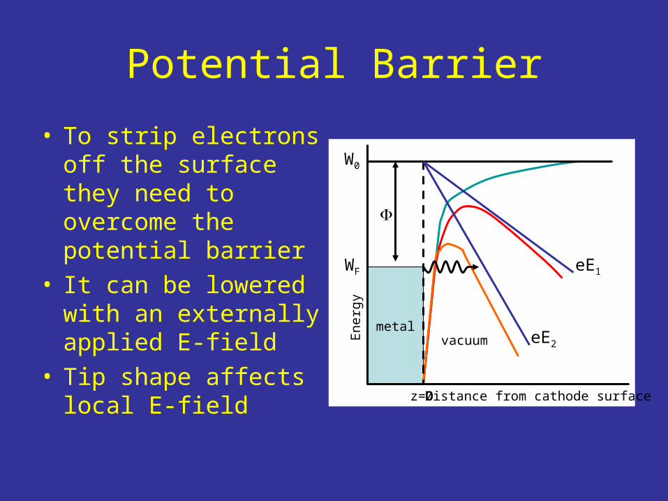
• To strip electrons off the surface they need to overcome the potential barrier
• It can be lowered with an externally applied E-field
• Tip shape affects local E-field
metal
W0
WF eE1
eE2E
nerg
y
Distance from cathode surface z=0
vacuum
Phosphor Screens
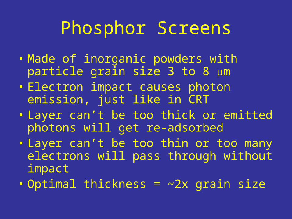
• Made of inorganic powders with particle grain size 3 to 8 m
• Electron impact causes photon emission, just like in CRT
• Layer can’t be too thick or emitted photons will get re-adsorbed
• Layer can’t be too thin or too many electrons will pass through without impact
• Optimal thickness = ~2x grain size
Plasma Displays
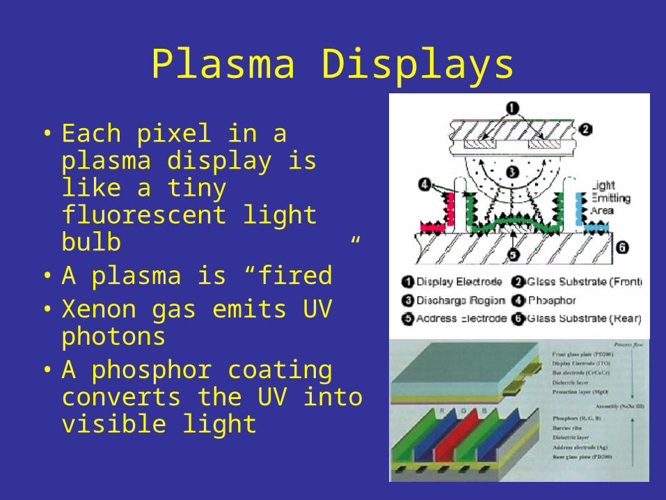
• Each pixel in a plasma display is like a tiny fluorescent light bulb
• A plasma is “fired”• Xenon gas emits UV
photons• A phosphor coating
converts the UV into visible light
Electronic Paper
• Ultimate goal of display technologies:– Emulate printed paper
• Ultra-low power• Perfectly bistable (keeps image with no power)• Flexible, foldable• High contrast ratio• Appear paper white• Lightweight• User-friendly
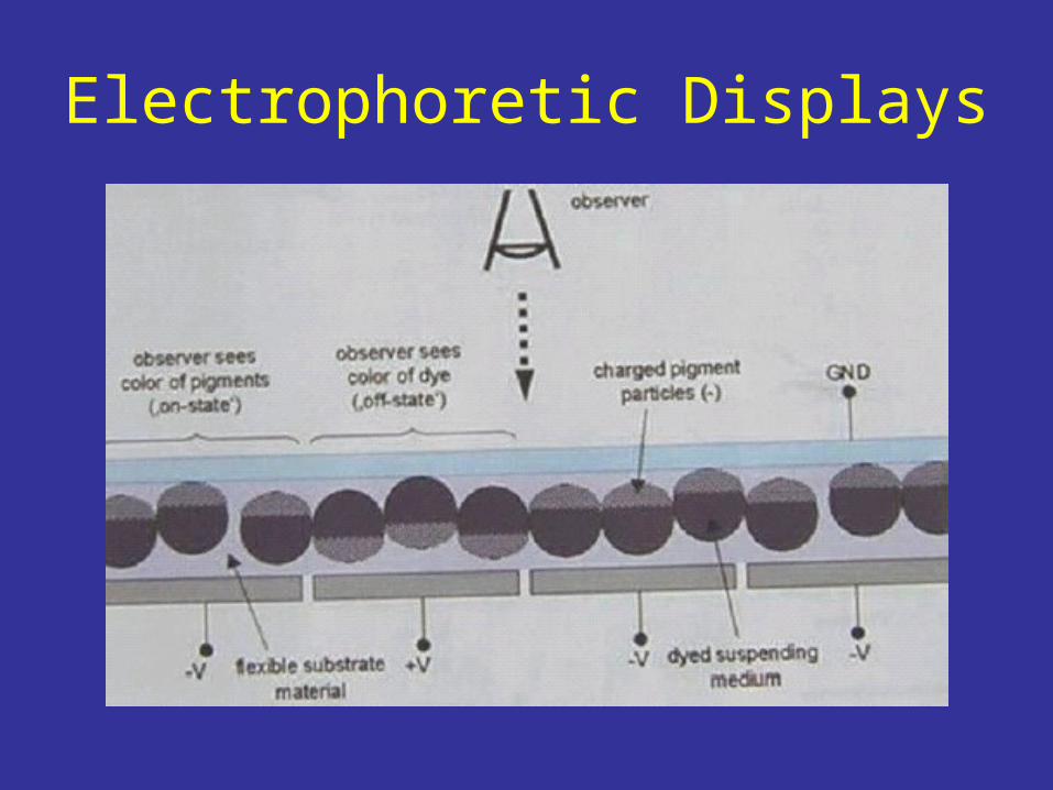
Electrophoretic Displays
• A solution of black dye and suspended white particles
• The white particles move in an applied E-field
• There’s a transparent electrode (ITO) and a back electrode
• Voltage is used to move the white particles to the surface for a white pixel, or to the bottom for a dark pixel
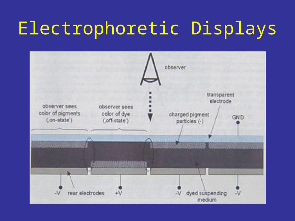
Electrophoretic Displays
Electrophoretic Displays
• Improvements can be made “microencapsulating” dye and pigment
• Prevents lateral motion between pixels
• Pigments tend to want to stick together under high field– Microcapsules prevent agglomeration of sizes
bigger than the capsule– Improves display lifetime
Electrophoretic Displays
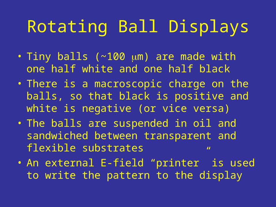
Rotating Ball Displays
• Tiny balls (~100 m) are made with one half white and one half black
• There is a macroscopic charge on the balls, so that black is positive and white is negative (or vice versa)
• The balls are suspended in oil and sandwiched between transparent and flexible substrates
• An external E-field “printer” is used to write the pattern to the display
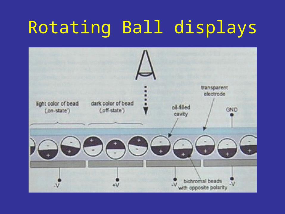
Rotating Ball displays
Thank You!
• This presentation will be available on the web.
Related Documents


