Introduction to the Altera Nios II Soft Processor This tutorial presents an introduction to Altera’s Nios R II processor, which is a soft processor that can be in- stantiated on an Altera FPGA device. It describes the basic architecture of Nios II and its instruction set. The Nios II processor and its associated memory and peripheral components are easily instantiated by using Altera’s SOPC Builder in conjuction with the Quartus R II software. A full desciption of the Nios II processor is provided in the Nios II Processor Reference Handbook , which is avail able in the lite ratu re section of the Alte ra web site . An introdu ctio n to the SOPC Builde r is giv en in the tutorial Intr oduction to the Altera SOPC Builder , which can be found in the University Program section of the web site. Contents: Nios II System Overview of Nios II Processor Features Register Structure Accessing Memory and I/O Devices Addressing Instruction Set Assembler Directiv es Example Program Exception Processing Cache Memory Tightly Coupled Memory 1

Welcome message from author
This document is posted to help you gain knowledge. Please leave a comment to let me know what you think about it! Share it to your friends and learn new things together.
Transcript

8/3/2019 Tut Nios2 Introduction
http://slidepdf.com/reader/full/tut-nios2-introduction 1/22
Introduction to the Altera Nios II Soft Processor
This tutorial presents an introduction to Altera’s Nios R II processor, which is a soft processor that can be in-
stantiated on an Altera FPGA device. It describes the basic architecture of Nios II and its instruction set. The Nios
II processor and its associated memory and peripheral components are easily instantiated by using Altera’s SOPC
Builder in conjuction with the Quartus R II software.
A full desciption of the Nios II processor is provided in the Nios II Processor Reference Handbook , which
is available in the literature section of the Altera web site. An introduction to the SOPC Builder is given in thetutorial Introduction to the Altera SOPC Builder , which can be found in the University Program section of the web
site.
Contents:
Nios II System
Overview of Nios II Processor Features
Register Structure
Accessing Memory and I/O Devices
Addressing
Instruction Set
Assembler Directives
Example Program
Exception Processing
Cache Memory
Tightly Coupled Memory
1
8/3/2019 Tut Nios2 Introduction
http://slidepdf.com/reader/full/tut-nios2-introduction 2/22
Altera’s Nios II is a soft processor, defined in a hardware description language, which can be implemented in
Altera’s FPGA devices by using the Quartus R II CAD system. This tutorial provides a basic introduction to the
Nios II processor, intended for a user who wishes to implement a Nios II based system on the Altera DE2 board.
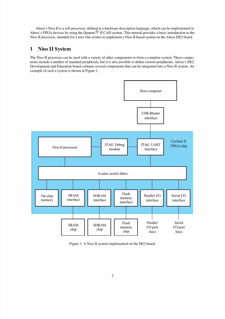
1 Nios II System
The Nios II processor can be used with a variety of other components to form a complete system. These compo-
nents include a number of standard peripherals, but it is also possible to define custom peripherals. Altera’s DE2
Development and Education board contains several components that can be integrated into a Nios II system. An
example of such a system is shown in Figure 1.
On-chipmemory
interface
SDRAMinterface
Flashmemory
Parallel I/O
interface
Serial I/O
interface
SRAMinterface
SRAM
chipSDRAM
chipchip
Flashmemory
Avalon switch fabric
Nios II processor JTAG UART
interface
USB-Blaster
interface
Host computer
lines
ParallelI/O port
lines
SerialI/O port
Cyclone II
FPGA chipJTAG Debug
module
Figure 1. A Nios II system implemented on the DE2 board.
2

8/3/2019 Tut Nios2 Introduction
http://slidepdf.com/reader/full/tut-nios2-introduction 3/22
The Nios II processor and the interfaces needed to connect to other chips on the DE2 board are implemented in
the Cyclone II FPGA chip. These components are interconnected by means of the interconnection network called
the Avalon Switch Fabric. Memory blocks in the Cyclone II device can be used to provide an on-chip memory for
the Nios II processor. They can be connected to the processor either directly or through the Avalon network. The
SRAM and SDRAM memory chips on the DE2 board are accessed through the appropriate interfaces. Input/output
interfaces are instantiated to provide connection to the I/O devices used in the system. A special JTAG UART
interface is used to connect to the circuitry that provides a Universal Serial Bus (USB) link to the host computer towhich the DE2 board is connected. This circuitry and the associated software is called the USB-Blaster . Another
module, called the JTAG Debug module, is provided to allow the host computer to control the Nios II processor.
It makes it possible to perform operations such as downloading programs into memory, starting and stopping
execution, setting program breakpoints, and collecting real-time execution trace data.
Since all parts of the Nios II system implemented on the FPGA chip are defined by using a hardware description
language, a knowledgeable user could write such code to implement any part of the system. This would be an
onnerous and time consuming task. Instead, one can use the SOPC Builder tool in the Quartus II software to
implement a desired system simply by choosing the required components and specifying the parameters needed
to make each component fit the overall requirements of the system.
2 Overview of Nios II Processor Features
The Nios II processor has a number of features that can be configured by the user to meet the demands of a desired
system. The processor can be implemented in three different configurations:
• Nios II/f is a "fast" version designed for superior performance. It has the widest scope of configuration
options that can be used to optimize the processor for performance.
• Nios II/s is a "standard" version that requires less resources in an FPGA device as a trade-off for reduced
performance.
• Nios II/e is an "economy" version which requires the least amount of FPGA resources, but also has the most
limited set of user-configurable features.
The Nios II processor has a Reduced Instruction Set Computer (RISC) architecture. Its arithmetic and logic
operations are performed on operands in the general purpose registers. The data is moved between the memory
and these registers by means of Load and Store instructions.
The wordlength of the Nios II processor is 32 bits. All registers are 32 bits long. Byte addresses in a 32-bit
word are assigned in little-endian style, in which the lower byte addresses are used for the less significant bytes
(the rightmost bytes) of the word.
The Nios II architecture uses separate instruction and data buses, which is often referred to as the Harvard
architecture.
A Nios II processor may operate in the following three modes:
• Supervisor mode – allows the processor to execute all instructions and perform all available functions. When
the processor is reset, it enters this mode.
• User mode – the intent of this mode is to prevent execution of some instructions that shoud be used forsystems purposes only. Some processor features are not accessible in this mode.
• Debug mode – is used by software debugging tools to implement features such as breakpoints and watch-
points.
Application programs can be run in either the User or Supervisor modes. Presently available versions of the Nios
II processor do not support the User mode.
3

8/3/2019 Tut Nios2 Introduction
http://slidepdf.com/reader/full/tut-nios2-introduction 4/22
3 Register Structure
The Nios II processor has thirty two 32-bit general purpose registers, as shown in Figure 2. Some of these registers
are intended for a specific purpose and have special names that are recognized by the Assembler.
• Register r0 is referred to as the zero register. It always contains the constant 0. Thus, reading this register
returns the value 0, while writing to it has no effect.
• Register r1 is used by the Assembler as a temporary register; it should not be referenced in user programs
• Registers r24 and r29 are used for processing of exceptions; they are not available in User mode
• Registers r25 and r30 are used exclusively by the JTAG Debug module
• Registers r27 and r28 are used to control the stack used by the Nios II processor
• Register r31 is used to hold the return address when a subroutine is called
Register Name Function
r0 zero 0x00000000r1 at Assembler Temporary
r2
r3
· · ·
· · ·
· · ·
r23
r24 et Exception Temporary (1)
r25 bt Breakpoint Temporary (2)
r26 gp Global Pointer
r27 sp Stack Pointer
r28 fp Frame Pointer
r29 ea Exception Return Address (1)
r30 ba Breakpoint Return Address (2)
r31 ra Return Address
(1) The register is not available in User mode
(2) The register is used exclusively by the JTAG Debug module
Figure 2. General Purpose registers.
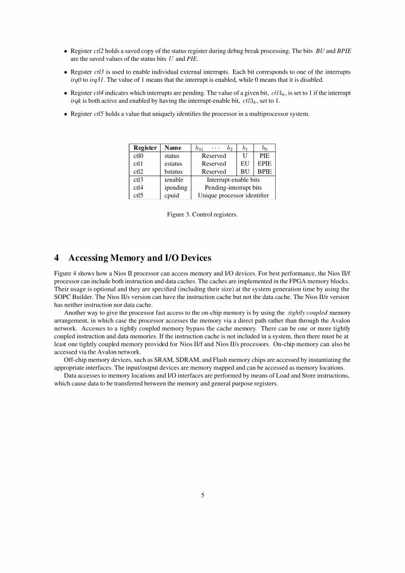
There are six 32-bit control registers, as indicated in Figure 3. The names given in the figure are recognized
by the Assembler. These registers are used automatically for control purposes. They can be read and written to by
special instructions rdctl and wrctl, which can be executed only in the supervisor mode. The registers are used asfollows:
• Register ctl0 reflects the operating status of the processor. Only two bits of this register are meaningful:
– U is the User/Supervisor mode bit; U = 1 for User mode, while U = 0 for Supervisor mode.
– PIE is the processor interrupt-enable bit. When PIE = 1, the processor may accept external interrupts.
When PIE = 0, the processor ignores external interrupts.
• Register ctl1 holds a saved copy of the status register during exception processing. The bits EU and EPIE
are the saved values of the status bits U and PIE .
4
8/3/2019 Tut Nios2 Introduction
http://slidepdf.com/reader/full/tut-nios2-introduction 5/22
• Register ctl2 holds a saved copy of the status register during debug break processing. The bits BU and BPIE
are the saved values of the status bits U and PIE .
• Register ctl3 is used to enable individual external interrupts. Each bit corresponds to one of the interrupts
irq0 to irq31. The value of 1 means that the interrupt is enabled, while 0 means that it is disabled.
• Register ctl4 indicates which interrupts are pending. The value of a given bit, ctl4k, is set to 1 if the interrupt
irqk is both active and enabled by having the interrupt-enable bit, ctl3k, set to 1.
• Register ctl5 holds a value that uniquely identifies the processor in a multiprocessor system.
Register Name b31 · · · b2 b1 b0
ctl0 status Reserved U PIE
ctl1 estatus Reserved EU EPIE
ctl2 bstatus Reserved BU BPIE
ctl3 ienable Interrupt-enable bits
ctl4 ipending Pending-interrupt bits
ctl5 cpuid Unique processor identifier
Figure 3. Control registers.
4 Accessing Memory and I/O Devices
Figure 4 shows how a Nios II processor can access memory and I/O devices. For best performance, the Nios II/f
processor can include both instruction and data caches. The caches are implemented in the FPGA memory blocks.
Their usage is optional and they are specified (including their size) at the system generation time by using the
SOPC Builder. The Nios II/s version can have the instruction cache but not the data cache. The Nios II/e version
has neither instruction nor data cache.
Another way to give the processor fast access to the on-chip memory is by using the tightly coupled memory
arrangement, in which case the processor accesses the memory via a direct path rather than through the Avalon
network. Accesses to a tightly coupled memory bypass the cache memory. There can be one or more tightly
coupled instruction and data memories. If the instruction cache is not included in a system, then there must be at
least one tightly coupled memory provided for Nios II/f and Nios II/s processors. On-chip memory can also be
accessed via the Avalon network.
Off-chip memory devices, such as SRAM, SDRAM, and Flash memory chips are accessed by instantiating the
appropriate interfaces. The input/output devices are memory mapped and can be accessed as memory locations.
Data accesses to memory locations and I/O interfaces are performed by means of Load and Store instructions,
which cause data to be transferred between the memory and general purpose registers.
5

8/3/2019 Tut Nios2 Introduction
http://slidepdf.com/reader/full/tut-nios2-introduction 6/22
Tightly coupled instruction memory
I/O
interface
Tightly coupled
data memory
Memoryinterface
Memory
device
Avalon switch fabric
Data
cache
Cyclone II
FPGA chip
Instruction
cache
I/O
device
Instruction bus selector logic Data bus selector logic
General purpose
registersProgram counter
Figure 4. Memory and I/O organization.
5 Addressing
The Nios II processor issues 32-bit addresses. The memory space is byte-addressable. Instructions can read and
write words (32 bits), halfwords (16 bits), or bytes (8 bits) of data. Reading or writing to an address that does not
correspond to an existing memory or I/O location produces an undefined result.
There are five addressing modes provided:
• Immediate mode – a 16-bit operand is given explicitly in the instruction. This value may be sign extended
to produce a 32-bit operand in instructions that perform arithmetic operations.
• Register mode – the operand is in a processor register
• Displacement mode – the effective address of the operand is the sum of the contents of a register and a
signed 16-bit displacement value given in the instruction
• Register indirect mode – the effective address of the operand is the contents of a register specified in the
instruction. This is equivalent to the displacement mode where the displacement value is equal to 0.
6

8/3/2019 Tut Nios2 Introduction
http://slidepdf.com/reader/full/tut-nios2-introduction 7/22
• Absolute mode – a 16-bit absolute address of an operand can be specified by using the displacement mode
with register r0 which always contains the value 0.
6 Instructions
All Nios II instructions are 32-bits long. In addition to machine instructions that are executed directly by the pro-
cessor, the Nios II instruction set includes a number of pseudoinstructions that can be used in assembly language
programs. The Assembler replaces each pseudoinstruction by one or more machine instructions.
Figure 5 depicts the three possible instruction formats: I-type, R-type and J-type. In all cases the six bits b5−0
denote the OP code. The remaining bits are used to specify registers, immediate operands, or extended OP codes.
• I-type – Five-bit fields A and B are used to specify general purpose registers. A 16-bit field IMMED16
provides immediate data which can be sign extended to provide a 32-bit operand.
• R-type – Five-bit fields A, B and C are used to specify general purpose registers. An 11-bit field OPX is
used to extend the OP code.
• J-type – A 26-bit field IMMED26 contains an unsigned immediate value. This format is used only in the
Call instruction.
0562122262731
OPIMMED16BA
0562122262731
OPBA
(a) I-type
05631
OPIMMED26
(b) R-type
(c) J-type
1617
OPXC
Figure 5. Formats of Nios II instructions.
The following subsections discuss briefly the main features of the Nios II instruction set. For a complete
description of the instruction set, including the details of how each instruction is encoded, the reader should
consult the Nios II Processor Reference Handbook .
6.1 Load and Store Instructions
Load and Store instructions are used to move data between memory (and I/0 interfaces) and the general purpose
registers. They are of I-type. For example, the Load Word instruction
ldw rB, byte_offset(rA)
7

8/3/2019 Tut Nios2 Introduction
http://slidepdf.com/reader/full/tut-nios2-introduction 8/22
determines the effective address of a memory location as the sum of a byte_offset value and the contents of register
A. The 16-bit byte_offset value is sign extended to 32 bits. The 32-bit memory operand is loaded into register B.
For instance, assume that the contents of register r4 are 126010 and the byte_offset value is 8010. Then, the
instruction
ldw r3, 80(r4)
loads the 32-bit operand at memory address 134010 into register r3.
The Store Word instruction has the format
stw rB, byte_offset(rA)
It stores the contents of register B into the memory location at the address computed as the sum of the byte_offset
value and the contents of register A.
There are Load and Store instructions that use operands that are only 8 or 16 bits long. They are referred to as
Load/Store Byte and Load/Store Halfword instructions, respectively. Such Load instructions are:
• ldb (Load Byte)
• ldbu (Load Byte Unsigned)
• ldh (Load Halfword)
• ldhu (Load Halfword Unsigned)
When a shorter operand is loaded into a 32-bit register, its value has to be adjusted to fit into the register. This
is done by sign extending the 8- or 16-bit value to 32 bits in the ldb and ldh instructions. In the ldbu and ldhuinstructions the operand is zero extended.
The corresponding Store instructions are:
• stb (Store Byte)
• sth (Store Halfword)
The stb instruction stores the low byte of register B into the memory byte specified by the effective address. The
sth instruction stores the low halfword of register B. In this case the effective address must be halfword aligned.
Each Load and Store instruction has a version intended for accessing locations in I/O device interfaces. These
instructions are:
• ldwio (Load Word I/O)
• ldbio (Load Byte I/O)
• ldbuio (Load Byte Unsigned I/O)
• ldhio (Load Halfword I/O)
• ldhuio (Load Halfword Unsigned I/O)
• stwio (Store Word I/O)
• stbio (Store Byte I/O)
• sthio (Store Halfword I/O)
The difference is that these instructions bypass the cache, if one exists.
8

8/3/2019 Tut Nios2 Introduction
http://slidepdf.com/reader/full/tut-nios2-introduction 9/22
6.2 Arithmetic Instructions
The arithmetic instructions operate on the data that is either in the general purpose registers or given as an imme-
diate value in the instruction. These instructions are of R-type or I-type, respectively. They include:
• add (Add Registers)
• addi (Add Immediate)• sub (Subtract Registers)
• subi (Subtract Immediate)
• mul (Multiply)
• muli (Multiply Immediate)
• div (Divide)
• divu (Divide Unsigned)
The Add instruction
add rC, rA, rB
adds the contents of registers A and B, and places the sum into register C .
The Add Immediate instruction
addi rB, rA, IMMED16
adds the contents of register A and the sign-extended 16-bit operand given in the instruction, and places the result
into register B. The addition operation in these instructions is the same for both signed and unsigned operands;
there are no condition flags that are set by the operation. This means that when unsigned operands are added, the
carry from the most significant bit position has to be detected by executing a separate instruction. Similarly, when
signed operands are added, the arithmetic overflow has to be detected separately. The detection of these conditions
is dicussed in section 6.11.
The Subtract instruction
sub rC, rA, rB
subtracts the contents of register B from register A, and places the result into register C . Again, the carry and
overflow detection has to be done by using additional instructions, as explained in section 6.11.
The immediate version, subi, is a pseudoinstruction implemented as
addi rB, rA, -IMMED16
The Multiply instruction
mul rC, rA, rB
multiplies the contents of registers A and B, and places the low-order 32 bits of the product into register C . The
operands are treated as unsigned numbers. The carry and overflow detection has to be done by using additional
instructions. In the immediate version
muli rB, rA, IMMED16
the 16-bit immediate operand is sign extended to 32 bits.
9

8/3/2019 Tut Nios2 Introduction
http://slidepdf.com/reader/full/tut-nios2-introduction 10/22
The Divide instruction
div rC, rA, rB
divides the contents of register A by the contents of register B and places the integer portion of the quotient into
register C . The operands are treated as signed integers. The divu instruction is performed in the same way except
that the operands are treated as unsigned integers.
6.3 Logic Instructions
The logic instructions provide the AND, OR, XOR, and NOR operations. They operate on data that is either in
the general purpose registers or given as an immediate value in the instruction. These instructions are of R-type or
I-type, respectively.
The AND instruction
and rC, rA, rB
performs a bitwise logical AND of the contents of registers A and B, and stores the result in register C . Similarly,
the instructions or, xor and nor perform the OR, XOR and NOR operations, respectively.
The AND Immediate instruction
andi rB, rA, IMMED16
performs a bitwise logical AND of the contents of register A and the IMMED16 operand which is zero-extended
to 32 bits, and stores the result in register B. Similarly, the instructions ori, xori and nori perform the OR, XOR
and NOR operations, respectively.
It is also possible to use the 16-bit immediate operand as the 16 high-order bits in the logic operations, in which
case the low-order 16 bits of the operand are zeros. This is accomplished with the instructions:
• andhi (AND High Immediate)
• orhi (OR High Immediate)
• xorhi (XOR High Immediate)
6.4 Move Instructions
The Move instructions copy the contents of one register into another, or they place an immediate value into a
register. They are pseudoinstructions implemented by using other instructions. The instruction
mov rC, rA
copies the contents of register A into register C . It is implemented as
add rC, rA, r0
The Move Immediate instruction
movi rB, IMMED16
sign extends the IMMED16 value to 32 bits and loads it into register B. It is implemented as
addi rB, r0, IMMED16
The Move Unsigned Immediate instruction
10

8/3/2019 Tut Nios2 Introduction
http://slidepdf.com/reader/full/tut-nios2-introduction 11/22
movui rB, IMMED16
zero extends the IMMED16 value to 32 bits and loads it into register B. It is implemented as
ori rB, r0, IMMED16
The Move Immediate Address instruction
movia rB, LABEL
loads a 32-bit value that corresponds to the address LABEL into register B. It is implemented as:
orhi rB, r0, %hi(LABEL)ori rB, rB, %lo(LABEL)
The %hi(LABEL) and %lo(LABEL) are the Assembler macros which extract the high-order 16 bits and the low-
order 16 bits, respectively, of a 32-bit value LABEL. The orhi instruction sets the high-order bits of register B,
followed by the ori instruction which sets the low-order bits of B. Note that two instructions are used because the
I-type format provides for only a 16-bit immediate operand.
6.5 Comparison Instructions
The Comparison instructions compare the contents of two registers or the contents of a register and an immediate
value, and write either 1 (if true) or 0 (if false) into the result register. They are of R-type or I-type, respectively.
These instructions correspond to the equality and relational operators in the C programming language.
The Compare Less Than Signed instruction
cmplt rC, rA, rB
performs the comparison of signed numbers in registers A and B, rA < rB, and writes a 1 into register C if the
result is true; otherwise, it writes a 0.
The Compare Less Than Unsigned instruction
cmpltu rC, rA, rB
performs the same function as the cmplt instruction, but it treats the operands as unsigned numbers.
Other instructions of this type are:
• cmpeq rC, rA, rB (Comparison rA == rB)
• cmpne rC, rA, rB (Comparison rA != rB)
• cmpge rC, rA, rB (Signed comparison rA >= rB)
• cmpgeu rC, rA, rB (Unsigned comparison rA >= rB)
• cmpgt rC, rA, rB (Signed comparison rA > rB)
This is a pseudoinstruction implemented as the cmplt instruction by swapping its rA and rB operands.
• cmpgtu rC, rA, rB (Unsigned comparison rA > rB)
This is a pseudoinstruction implemented as the cmpltu instruction by swapping its rA and rB operands.
• cmple rC, rA, rB (Signed comparison rA <= rB)
This is a pseudoinstruction implemented as the cmpge instruction by swapping its rA and rB operands.
• cmpleu rC, rA, rB (Unsigned comparison rA <= rB)
This is a pseudoinstruction implemented as the cmpgeu instruction by swapping its rA and rB operands.
11

8/3/2019 Tut Nios2 Introduction
http://slidepdf.com/reader/full/tut-nios2-introduction 12/22
The immediate versions of the Comparison instructions involve an immediate operand. For example, the
Compare Less Than Signed Immediate instruction
cmplti rB, rA, IMMED16
compares the signed number in register A with the sign-extended immediate operand. It writes a 1 into register B
if rA < IMMED16; otherwise, it writes a 0.
The Compare Less Than Unsigned Immediate instruction
cmpltui rB, rA, IMMED16
compares the unsigned number in register A with the zero-extended immediate operand. It writes a 1 into register
B if rA < IMMED16; otherwise, it writes a 0.
Other instructions of this type are:
• cmpeqi rB, rA, IMMED16 (Comparison rA == IMMED16)
• cmpnei rB, rA, IMMED16 (Comparison rA != IMMED16)
• cmpgei rB, rA, IMMED16 (Signed comparison rA>
= IMMED16)
• cmpgeui rB, rA, IMMED16 (Unsigned comparison rA >= IMMED16)
• cmpgti rB, rA, IMMED16 (Signed comparison rA > IMMED16)
This is a pseudoinstruction which is implemented by using the cmpgei instruction with an immediate value
IMMED16 + 1.
• cmpgtui rB, rA, IMMED16 (Unsigned comparison rA > IMMED16)
This is a pseudoinstruction which is implemented by using the cmpgeui instruction with an immediate
value IMMED16 + 1.
• cmplei rB, rA, IMMED16 (Signed comparison rA <= IMMED16)
This is a pseudoinstruction which is implemented by using the cmplti instruction with an immediate value
IMMED16 + 1.
• cmpleui rB, rA, IMMED16 (Unsigned comparison rA <= IMMED16)
This is a pseudoinstruction which is implemented by using the cmpltui instruction with an immediate value
IMMED16 + 1.
6.6 Shift Instructions
The Shift instructions shift the contents of a register either to the right or to the left. They are of R-type. They
correspond to the shift operators, >> and <<, in the C programming language. These instructions are:
• srl rC, rA, rB (Shift Right Logical)
• srli rC, rA, IMMED5 (Shift Right Logical Immediate)
• sra rC, rA, rB (Shift Right Arithmetic)
• srai rC, rA, IMMED5 (Shift Right Arithmetic Immediate)
• sll rC, rA, rB (Shift Left Logical)
• slli rC, rA, IMMED5 (Shift Left Logical Immediate)
12
8/3/2019 Tut Nios2 Introduction
http://slidepdf.com/reader/full/tut-nios2-introduction 13/22
The srl instruction shifts the contents of register A to the right by the number of bit positions specified by the five
least-significant bits (number in the range 0 to 31) in register B, and stores the result in register C . The vacated
bits on the left side of the shifted operand are filled with 0s.
The srli instruction shifts the contents of register A to the right by the number of bit positions specified by the
five-bit unsigned value, IMMED5, given in the instruction.
The sra and srai instructions perform the same actions as the srl and srli instructions, except that the sign bit,
rA31, is replicated into the vacated bits on the left side of the shifted operand.
The sll and slli instructions are similar to the srl and srli instructions, but they shift the operand in register A to the
left and fill the vacated bits on the right side with 0s.
6.7 Rotate Instructions
There are three Rotate instructions, which use the R-type format:
• ror rC, rA, rB (Rotate Right)
• rol rC, rA, rB (Rotate Left)
• roli rC, rA, IMMED5 (Rotate Left Immediate)
The ror instruction rotates the bits of register A in the left-to-right direction by the number of bit positions spec-
ified by the five least-significant bits (number in the range 0 to 31) in register B, and stores the result in register C .
The rol instruction is similar to the ror instruction, but it rotates the operand in the right-to-left direction.
The roli instruction rotates the bits of registerA in the right-to-left direction by the number of bit positions specified
by the five-bit unsigned value, IMMED5, given in the instruction, and stores the result in register C .
6.8 Branch and Jump Instructions
The flow of execution of a program can be changed by executing Branch or Jump instructions. It may be changedeither unconditionally or conditionally.
The Jump instruction
jmp rA
transfers execution unconditionally to the address contained in register A.
The Unconditional Branch instruction
br LABEL
transfers execution unconditionally to the instruction at address LABEL. This is an instruction of I-type, in which
a 16-bit immediate value (interpreted as a signed number) specifies the offset to the branch target instruction. Theoffset is the distance in bytes from the instruction that immediately follows br to the address LABEL.
Conditional transfer of execution is achieved with the Conditional Branch instructions, which compare the
contents of two registers and cause a branch if the result is true. These instructions are of I-type and the offset is
determined as explained above for the br instruction.
13

8/3/2019 Tut Nios2 Introduction
http://slidepdf.com/reader/full/tut-nios2-introduction 14/22
The Branch if Less Than Signed instruction
blt rA, rB, LABEL
performs the comparison rA < rB, treating the contents of the registers as signed numbers.
The Branch if Less Than Unsigned instruction
bltu rA, rB, LABEL
performs the comparison rA < rB, treating the contents of the registers as unsigned numbers.
The other Conditional Branch instructions are:
• beq rA, rB, LABEL (Comparison rA == rB)
• bne rA, rB, LABEL (Comparison rA != rB)
• bge rA, rB, LABEL (Signed comparison rA >= rB)
• bgeu rA, rB, LABEL (Unsigned comparison rA >= rB)
• bgt rA, rB, LABEL (Signed comparison rA > rB)This is a pseudoinstruction implemented as the blt instruction by swapping the register operands.
• bgtu rA, rB, LABEL (Unsigned comparison rA > rB)
This is a pseudoinstruction implemented as the bltu instruction by swapping the register operands.
• ble rA, rB, LABEL (Signed comparison rA <= rB)
This is a pseudoinstruction implemented as the bge instruction by swapping the register operands.
• bleu rA, rB, LABEL (Unsigned comparison rA <= rB)
This is a pseudoinstruction implemented as the bgeu instruction by swapping the register operands.
6.9 Subroutine Linkage Instructions
Nios II has two instructions for calling subroutines. The Call Subroutine instruction
call LABEL
is of J-type, which includes a 26-bit unsigned immediate value (IMMED26). The instruction saves the return
address (which is the address of the next instruction) in register r31. Then, it transfers control to the instruction
at address LABEL. This address is determined by concatenating the four high-order bits of the Program Counter
with the IMMED26 value as follows
Jump address = PC31−28 : IMMED26 : 00
Note that the two least-significant bits are 0 because Nios II instructions must be aligned on word boundaries.
The Call Subroutine in Register instruction
callr rA
is of R-type. It saves the return address in register r31 and then transfers control to the instruction at the address
contained in register A.
Return from a subroutine is performed with the instruction
ret
This instruction transfers execution to the address contained in register r31.
14

8/3/2019 Tut Nios2 Introduction
http://slidepdf.com/reader/full/tut-nios2-introduction 15/22
6.10 Control Instructions
The Nios II control registers can be read and written by special instructions. The Read Control Register instruction
rdctl rC, ctlN
copies the contents of control register ctlN into register C .
The Write Control Register instruction
wrctl ctlN, rA
copies the contents of register A into the control register ctlN .
There are two instructions provided for dealing with exceptions: trap and eret. They are similar to the call
and ret instructions, but they are used for exceptions. Their use is discussed in section 8.2.
The instructions break and bret generate breaks and return from breaks. They are used exclusively by the
software debugging tools.
The Nios II cache memories are managed with the instructions: flushd (Flush Data Cache Line), flushi (Flush
Instruction Cache Line), initd (Initialize Data Cache Line), and initi (Initialize Instruction Cache Line). Theseinstructions are discussed in section 9.1.
6.11 Carry and Overflow Detection
As pointed out in section 6.2, the Add and Subtract instructions perform the corresponding operations in the same
way for both signed and unsigned operands. The possible carry and arithmetic overflow conditions are not de-
tected, because Nios II does not contain condition flags that might be set as a result. These conditions can be
detected by using additional instructions.
Consider the Add instruction
add rC, rA, rB
Having executed this instruction, a possible occurrence of a carry out of the most-significant bit (C 31) can be
detected by checking whether the unsigned sum (in register C ) is less than one of the unsigned operands. For
example, if this instruction is followed by the instruction
cmpltu rD, rC, rA
then the carry bit will be written into register D.
Similarly, if a branch is required when a carry occurs, this can be accomplished as follows:
add rC, rA, rBbltu rC, rA, LABEL
A test for arithmetic overflow can be done by checking the signs of the summands and the resulting sum. An
overflow occurs if two positive numbers produce a negative sum, or if two negative numbers produce a positive
sum. Using this approach, the overflow condition can control a conditional branch as follows:
add rC, rA, rB /* The required Add operation */
xor rD, rC, rA /* Compare signs of sum and rA */
xor rE, rC, rB /* Compare signs of sum and rB */
and rD, rD, rE /* Set D31 = 1 if ((A31 == B31) ! = C 31) */
blt rD, r0, LABEL /* Branch if overflow occurred */
15

8/3/2019 Tut Nios2 Introduction
http://slidepdf.com/reader/full/tut-nios2-introduction 16/22
A similar approach can be used to detect the carry and overflow conditions in Subtract operations. A carry out
of the most-significant bit of the resulting difference can be detected by checking whether the first operand is less
than the second operand. Thus, the carry can be used to control a conditional branch as follows:
sub rC, rA, rB
bltu rA, rB, LABEL
The arithmetic overflow in a Subtract operation is detected by comparing the sign of the generated difference with
the signs of the operands. Overflow occurs if the operands in registers A and B have different signs, and the sign
of the difference in register C is different than the sign of A. Thus, a conditional branch based on the arithmetic
overflow can be achieved as follows:
sub rC, rA, rB /* The required Subtract operation */
xor rD, rA, rB /* Compare signs of rA and rB */
xor rE, rA, rC /* Compare signs of rA and rC */
and rD, rD, rE /* Set D31 = 1 if ((A31 ! = B31) && (A31 ! = C 31)) */
blt rD, r0, LABEL /* Branch if overflow occurred */
7 Assembler Directives
The Nios II Assembler conforms to the widely used GNU Assembler, which is software available in the public
domain. Thus, the GNU Assembler directives can be used in Nios II programs. Assembler directives begin with a
period. We describe some of the more frequently used assembler directives below.
.ascii "string"...
A string of ASCII characters is loaded into consecutive byte addresses in the memory. Multiple strings, separated
by commas, can be specified.
.asciz "string"...
This directive is the same as .ascii, except that each string is followed (terminated) by a zero byte.
.byte expressions
Expressions separated by commas are specified. Each expression is assembled into the next byte. Examples of
expressions are: 8, 5 + LABEL, and K − 6.
.data
Identifies the data that should be placed in the data section of the memory. The desired memory location for the
data section can be specified in the Altera Monitor Program’s system configuration window.
.end
Marks the end of the source code file; everything after this directive is ignored by the assembler.
.equ symbol, expression
Sets the value of symbol to expression.
16

8/3/2019 Tut Nios2 Introduction
http://slidepdf.com/reader/full/tut-nios2-introduction 17/22
.global symbol
Makes symbol visible outside the assembled object file.
.hword expressions
Expressions separated by commas are specified. Each expression is assembled into a 16-bit number.
.include " filename"
Provides a mechanism for including supporting files in a source program.
.org new-lc
Advances the location counter by new-lc, where new-lc is used as an offset from the starting location specified
in the Altera Monitor Program’s system configuration window. The .org directive may only increase the location
counter, or leave it unchanged; it cannot move the location counter backwards.
.skip size
Emits the number of bytes specified in size; the value of each byte is zero.
.text
Identifies the code that should be placed in the text section of the memory. The desired memory location for the
text section can be specified in the Altera Monitor Program’s system configuration window.
.word expressions
Expressions separated by commas are specified. Each expression is assembled into a 32-bit number.
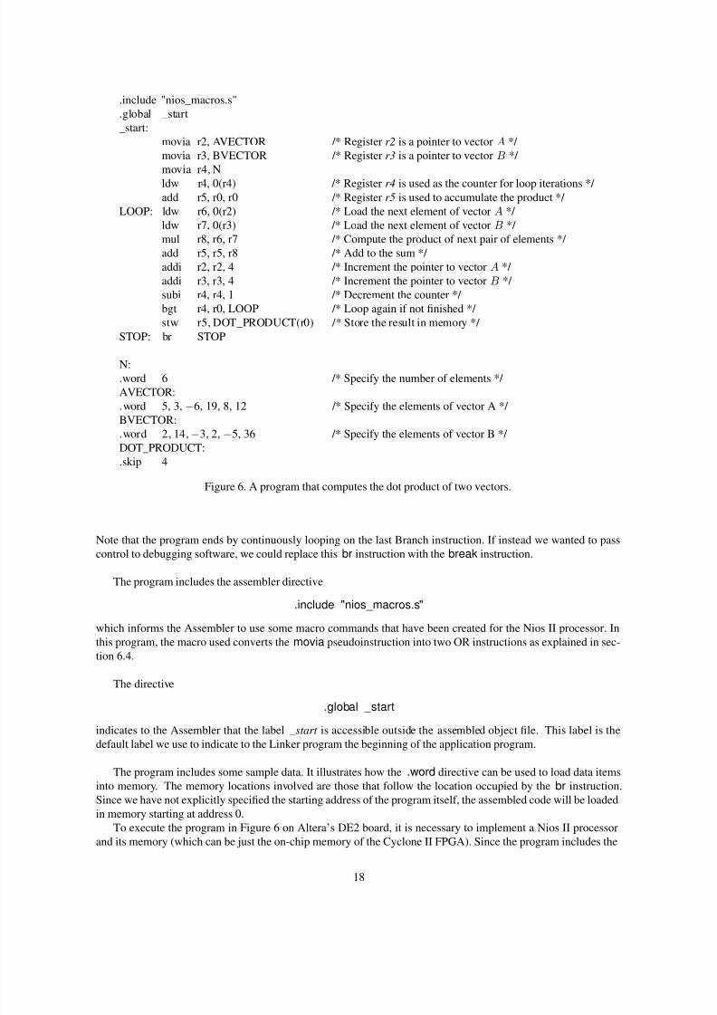
8 Example Program
As an illustration of Nios II instructions and assembler directives, Figure 6 gives an assembly language program
that computes a dot product of two vectors, A and B. The vectors have n elements. The required computation is
Dot product =n−1
i=0A(i) × B(i)
The vectors are stored in memory locations at addresses AVECTOR and BVECTOR, respectively. The number of el-
ements,n, is stored in memory locationN . The computed result is written into memory location DOT_PRODUCT .
Each vector element is assumed to be a signed 32-bit number.
17
8/3/2019 Tut Nios2 Introduction
http://slidepdf.com/reader/full/tut-nios2-introduction 18/22
.include "nios_macros.s"
.global _start
_start:
movia r2, AVECTOR /* Register r2 is a pointer to vector A */
movia r3, BVECTOR /* Register r3 is a pointer to vector B */
movia r4, N
ldw r4, 0(r4) /* Register r4 is used as the counter for loop iterations */
add r5, r0, r0 /* Register r5 is used to accumulate the product */
LOOP: ldw r6, 0(r2) /* Load the next element of vector A */
ldw r7, 0(r3) /* Load the next element of vector B */
mul r8, r6, r7 /* Compute the product of next pair of elements */
add r5, r5, r8 /* Add to the sum */
addi r2, r2, 4 /* Increment the pointer to vector A */
addi r3, r3, 4 /* Increment the pointer to vector B */
subi r4, r4, 1 /* Decrement the counter */
bgt r4, r0, LOOP /* Loop again if not finished */
stw r5, DOT_PRODUCT(r0) /* Store the result in memory */
STOP: br STOP
N:
.word 6 /* Specify the number of elements */
AVECTOR:
.word 5, 3, −6, 19, 8, 12 /* Specify the elements of vector A */
BVECTOR:
.word 2, 14, −3, 2, −5, 36 /* Specify the elements of vector B */
DOT_PRODUCT:
.skip 4
Figure 6. A program that computes the dot product of two vectors.
Note that the program ends by continuously looping on the last Branch instruction. If instead we wanted to pass
control to debugging software, we could replace this br instruction with the break instruction.
The program includes the assembler directive
.include "nios_macros.s"
which informs the Assembler to use some macro commands that have been created for the Nios II processor. In
this program, the macro used converts the movia pseudoinstruction into two OR instructions as explained in sec-
tion 6.4.
The directive
.global _startindicates to the Assembler that the label _start is accessible outside the assembled object file. This label is the
default label we use to indicate to the Linker program the beginning of the application program.
The program includes some sample data. It illustrates how the .word directive can be used to load data items
into memory. The memory locations involved are those that follow the location occupied by the br instruction.
Since we have not explicitly specified the starting address of the program itself, the assembled code will be loaded
in memory starting at address 0.
To execute the program in Figure 6 on Altera’s DE2 board, it is necessary to implement a Nios II processor
and its memory (which can be just the on-chip memory of the Cyclone II FPGA). Since the program includes the
18
8/3/2019 Tut Nios2 Introduction
http://slidepdf.com/reader/full/tut-nios2-introduction 19/22
Multiply instruction, it cannot be executed on the economy version of the processor, because Nios II/e does not
support the mul instruction. Either Nios II/s or Nios II/f processors can be used.
The tutorial Introduction to the Altera SOPC Builder explains how a Nios II system can be implemented.
The tutorial Altera Monitor Program explains how an application program can be assembled, downloaded and
executed on the DE2 board.
9 Exception Processing
An exception in the normal flow of program execution can be caused by:
• Software trap
• Hardware interrupt
• Unimplemented instruction
In response to an exception the Nios II processor performs the following actions:
1. Saves the existing processor status information by copying the contents of the status register (ctl0) into the
estatus register (ctl1)
2. Clears the U bit in the status register, to ensure that the processor is in the Supervisor mode
3. Clears the PIE bit in the status register, thus disabling the additional external processor interrupts
4. Writes the address of the instruction after the exception into the ea register (r29)
5. Transfers execution to the address of the exception handler which determines the cause of the exception and
dispatches an appropriate exception routine to respond to the exception
The address of the exception handler is specified at system generation time using the SOPC Builder, and it cannot
be changed by software at run time. This address can be provided by the designer; otherwise, the default address
is 2016 from the starting address of the main memory. For example, if the memory starts at address 0, then the
default address of the exception handler is 0x00000020.
9.1 Software Trap
A software exception occurs when a trap instruction is encountered in a program. This instruction saves the
address of the next instruction in the ea register (r29). Then, it disables interrupts and transfers execution to the
exception handler.
In the exception-service routine the last instruction is eret (Exception Return), which returns execution control
to the instruction that follows the trap instruction that caused the exception. The return address is given by the
contents of register ea. The eret instruction restores the previous status of the processor by copying the contents
of the estatus register into the status register.
A common use of the software trap is to transfer control to a different program, such as an operating system.
9.2 Hardware Interrupts
Hardware interrupts can be raised by external sources, such as I/O devices, by asserting one of the processor’s 32
interrupt-request inputs, irq0 through irq31. An interrupt is generated only if the following three conditions are
true:
• The PIE bit in the status register is set to 1
• An interrupt-request input, irqk , is asserted
• The corresponding interrupt-enable bit, ctl3k, is set to 1
19

8/3/2019 Tut Nios2 Introduction
http://slidepdf.com/reader/full/tut-nios2-introduction 20/22
The contents of the ipending register (ctl4) indicate which interrupt requests are pending. An exception routine
determines which of the pending interrupts has the highest priority, and transfers control to the corresponding
interrupt-service routine.
Upon completion of the interrupt-service routine, the execution control is returned to the interrupted program
by means of the eret instruction, as explained above. However, since an external interrupt request is handled
without first completing the instruction that is being executed when the interrupt occurs, the interrupted instruction
must be re-executed upon return from the interrupt-service routine. To achieve this, the interrupt-service routinehas to adjust the contents of the ea register which are at this time pointing to the next instruction of the interrupted
program. Hence, the value in the ea register has to be decremented by 4 prior to executing the eret instruction.
9.3 Unimplemented Instructions
This exception occurs when the processor encounters a valid instruction that is not implemented in hardware. This
may be the case with instructions such as mul and div. The exception handler may call a routine that emulates the
required operation in software.
9.4 Determining the Type of Exception
When an exception occurs, the exception-handling routine has to determine what type of exception has occurred.
The order in which the exceptions should be checked is:
1. Read the ipending register to see if a hardware interrupt has occurred; if so, then go to the appropriate
interrupt-service routine.
2. Read the instruction that was being executed when the exception occurred. The address of this instruction
is the value in the ea register minus 4. If this is the trap instruction, then go to the software-trap-handling
routine.
3. Otherwise, the exception is due to an unimplemented instruction.
9.5 Exception Processing Example
The following example illustrates the Nios II code needed to deal with a hardware interrupt. We will assume that
an I/O device raises an interrupt request on the interrupt-request input irq1. Also, let the exception handler start ataddress 0x020, and the interrupt-service routine for the irq1 request start at address 0x0100.
Figure 7 shows a portion of the code that can be used for this purpose. The exception handler first determines
the type of exception that has occurred. Having determined that there is a hardware interrupt request, it finds the
specific interrupt by examining the bits of the et register which has a copy of control register ctl4. If bit et1 is
equal to 1, then the the interrupt-service routine EXT_IRQ1 is executed. Otherwise, it is necessary to check for
other possible interrupts.
Note that in Figure 7 we are using register r13 in the process of testing whether the bit irq1 is set to 1. In a
practical application program this register may also be used for some other purpose, in which case its contents
should first be saved on the stack and later restored prior to returning from the exception handler.
20

8/3/2019 Tut Nios2 Introduction
http://slidepdf.com/reader/full/tut-nios2-introduction 21/22
.org 0x20
/* Exception handler */
rdctl et, ctl4 /* Check if external interrupt occurred */
beq et, r0, OTHER_EXCEPTIONS /* If zero, check exceptions */
subi ea, ea, 4 /* Hardware interrupt, decrement ea to execute the interrupted */
/* instruction upon return to main program */
andi r13, et, 2 /* Check if irq1 asserted */
bne r13, r0, EXT_IRQ1 /* If yes, go to IRQ1 service routine */
/* Instructions that check for other hardware interrupts should be placed here */
OTHER_EXCEPTIONS:
/* Instructions that check for other types of exceptions should be placed here */
.org 0x100
/* Interrupt-service routine for the desired hardware interrupt */
EXT_IRQ1:
/* Instructions that handle the irq1 interrupt request should be placed here */
eret /* Return from exception */
Figure 7. Code used to handle a hardware interrupt.
10 Cache Memory
As shown in Figure 4, a Nios II system can include instruction and data caches, which are implemented in the
memory blocks in the FPGA chip. The caches can be specified when a system is being designed by using the
SOPC Builder software. Inclusion of caches improves the performance of a Nios II system significantly, particu-
larly when most of the main memory is provided by an external SDRAM chip, as is the case with Altera’s DE2
board. Both instruction and data caches are direct-mapped.
The instruction cache can be implemented in the fast and standard versions of the Nios II processor systems.
It is organized in 8 words per cache line, and its size is a user-selectable design parameter.
The data cache can be implemented only with the Nios II/f processor. It has a configurable line size of 4, 16
or 32 bytes per cache line. Its overall size is also a user-selectable design parameter.
10.1 Cache Management
Cache management is handled by software. For this purpose the Nios II instruction set includes the following
instructions:
• initd IMMED16(rA) (Initialize data-cache line)
Invalidates the line in the data cache that is associated with the address determined by adding the sign-
extended value IMMED16 and the contents of register rA.
• initi rA (Initialize instruction-cache line)
Invalidates the line in the instruction cache that is associated with the address contained in register rA.
21

8/3/2019 Tut Nios2 Introduction
http://slidepdf.com/reader/full/tut-nios2-introduction 22/22
• flushd IMMED16(rA) (Flush data-cache line)
Computes the effective address by adding the sign-extended value IMMED16 and the contents of register
rA. Then, it identifies the cache line associated with this effective address, writes any dirty data in the cache
line back to memory, and invalidates the cache line.
• flushi rA (Flush instruction-cache line)
Invalidates the line in the instruction cache that is associated with the address contained in register rA.
10.2 Cache Bypass Methods
A Nios II processor uses its data cache in the standard manner. But, it also allows the cache to be bypassed in
two ways. As mentioned in section 6.1, the Load and Store instructions have a version intended for accessing I/O
devices, where the effective address specifies a location in an I/O device interface. These instructions are: ldwio,
ldbio, lduio, ldhio, ldhuio, stwio, stbio, and sthio. They bypass the data cache.
Another way of bypassing the data cache is by using bit 31 of an address as a tag that indicates whether the
processor should transfer the data to/from the cache, or bypass it. This feature is available only in the Nios II/f
processor.
Mixing cached and uncached accesses has to be done with care. Otherwise, the coherence of the cached data
may be compromised.
11 Tightly Coupled Memory
As explained in section 4, a Nios II processor can access the memory blocks in the FPGA chip as a tightly coupled
memory. This arrangement does not use the Avalon network. Instead, the tightly coupled memory is connected
directly to the processor.
Data in the tightly coupled memory is accessed using the normal Load and Store instructions, such as ldw or
stw. The Nios II control circuits determine if the address of a memory location is in the tightly coupled memory.
Accesses to the tightly coupled memory bypass the caches. For the address span of the tightly coupled memory,
the processor operates as if caches were not present.
Copyright c2008 Altera Corporation. All rights reserved. Altera, The Programmable Solutions Company, the
stylized Altera logo, specific device designations, and all other words and logos that are identified as trademarks
and/or service marks are, unless noted otherwise, the trademarks and service marks of Altera Corporation in
the U.S. and other countries. All other product or service names are the property of their respective holders.
Altera products are protected under numerous U.S. and foreign patents and pending applications, mask work
rights, and copyrights. Altera warrants performance of its semiconductor products to current specifications in
accordance with Altera’s standard warranty, but reserves the right to make changes to any products and services at
any time without notice. Altera assumes no responsibility or liability arising out of the application or use of any
information, product, or service described herein except as expressly agreed to in writing by Altera Corporation.
Altera customers are advised to obtain the latest version of device specifications before relying on any publishedinformation and before placing orders for products or services.
This document is being provided on an “as-is” basis and as an accommodation and therefore all warranties, rep-
resentations or guarantees of any kind (whether express, implied or statutory) including, without limitation, war-
ranties of merchantability, non-infringement, or fitness for a particular purpose, are specifically disclaimed.
Related Documents