UCC Library and UCC researchers have made this item openly available. Please let us know how this has helped you. Thanks! Title Manipulation of magnetic anisotropy in nanostructures Author(s) Maity, Tuhin Publication date 2015 Original citation Maity, T. S. 2015. Manipulation of magnetic anisotropy in nanostructures. PhD Thesis, University College Cork. Type of publication Doctoral thesis Rights © 2015, Tuhin S. Maity. http://creativecommons.org/licenses/by-nc-nd/3.0/ Item downloaded from http://hdl.handle.net/10468/2058 Downloaded on 2022-03-25T20:26:53Z

Welcome message from author
This document is posted to help you gain knowledge. Please leave a comment to let me know what you think about it! Share it to your friends and learn new things together.
Transcript
UCC Library and UCC researchers have made this item openly available.Please let us know how this has helped you. Thanks!
Title Manipulation of magnetic anisotropy in nanostructures
Author(s) Maity, Tuhin
Publication date 2015
Original citation Maity, T. S. 2015. Manipulation of magnetic anisotropy innanostructures. PhD Thesis, University College Cork.
Type of publication Doctoral thesis
Rights © 2015, Tuhin S. Maity.http://creativecommons.org/licenses/by-nc-nd/3.0/
Item downloadedfrom
http://hdl.handle.net/10468/2058
Downloaded on 2022-03-25T20:26:53Z
Ollscoil na hÉireann,
National University of Ireland
Manipulation of magnetic anisotropy in
nanostructures
A thesis undertaken
at the
Tyndall National Institute
And presented to the
National University of Ireland,
University College Cork
In partial fulfillment of the
requirements for the degree of Doctor of Philosophy (PhD)
by
Tuhin Subhra Maity BSc, MSc.
Supervisor: Dr. Saibal Roy
Co-Supervisor: Prof. John McInerney
2015

Contents
Acknowledgements ...................................................................................................... ii
List of figures ............................................................................................................... v
List of tables ................................................................................................................. x
Decleration .................................................................................................................. xi
Abstract ........................................................................................................................ 1
List of Publications ...................................................................................................... 4
Units ………………………………………………………………………………..8
1. Chapter – Introduction ......................................................................................... 9
1.1. Background ..................................................................................................... 9
1.2. Motivation of the work ................................................................................. 10
1.3. Defining the scope of the Thesis ................................................................... 10
1.4. Summary and Thesis Layout ........................................................................ 12
2. Chapter – State of the Art Review ..................................................................... 13
2.1. Introduction ................................................................................................... 13
2.2. Types of magnetic anisotropy ....................................................................... 18
2.2.1.Shape anisotropy ................................................................................... 18
2.2.2.Anisotropy due to domain alignment .................................................... 20
2.2.3.Crystalline anisotropy ........................................................................... 20
2.2.4.Textural anisotropy ............................................................................... 21
2.2.5.Exchange anisotropy ............................................................................. 22
2.2.6.Stress induced anisotropy ...................................................................... 23
2.2.7.Induced uniaxial anisotropy .................................................................. 23
2.3. Anisotropy control ........................................................................................ 24
2.3.1.Crystal structure .................................................................................... 24
2.3.2.Nanomodulation .................................................................................... 26
2.3.3.Exchange bias ....................................................................................... 30
2.3.3.1.Meiklejohn and Bean - Direct exchange ....................................... 33
2.3.3.2.Mauri - AFM spring: ..................................................................... 34
2.3.3.3.Malozemoff - Random field exchange .......................................... 35
2.3.3.4.Koon/Butler - Spin-flop coupling .................................................. 37
2.4. Different nanomagnetic phenomena out of nanostructures .......................... 38
2.4.1.Superparamagnetism ............................................................................. 38
2.4.2.Superferromagnetism ............................................................................ 39
2.4.3.Super Spin Glass ................................................................................... 39
2.4.3. Inverted hysteresis loop ....................................................................... 40
2.5. Sample preperation techniques ..................................................................... 40
2.5.1.Electrodeposition and electroplated magnetic materials-films… ……40
2.5.2. Sonochemical methods-nanocomposites ……………………………..42
2.6. Nanocomposite multiferroic materials – The current state of the art ........... 43
2.7. Exchange bias systems – The current state of the art ................................... 45
3 Chapter – Experimental techniques .................................................................... 47
3.1 Magnetic Characterizations of Materials ...................................................... 47
3.2 Structural characterization of materials ........................................................ 56
4 Chapter - Micromagnetic Simulations ............................................................... 66
4.1. Inreoduction .................................................................................................. 66
4.2. Micromagnetic theory………………………………………...…………….66
4.3. Energy terms in micromagnetic simulation .................................................. 66
4.4. Landau Lifshiftz Gilbert Equation ................................................................ 68
4.5. Length Scale ................................................................................................. 70
4.6. The Object Oriented MicroMagnetic Framework (OOMMF)...................... 72
5 Chapter – Manipulation of magnetic anisotropy-shape/dipolar ......................... 75
5.1. Introduction ................................................................................................... 75
5.2. Nanomodulated Ni45Fe55 electrodeposited thin film .................................... 77
5.3. Magnetic measurements of anisotropy manipulation ................................... 79
5.4. Micromagnetic simulation for anisotropy manipulation .............................. 84
5.5. Generalized anisotropy model for modulated thin film ................................ 94
5.6. Summary ....................................................................................................... 99
6 Chapter – Giant exchange bias in Bismuth ferrite (BFO) nanocomposite …...101
6.1. Introduction ................................................................................................. 101
6.2. BiFeO3-Bi2Fe4O9 nano-composite .............................................................. 102
6.2.1. Sample preperation…………………………………………………....102
6.2.2. Structural analysis ………………………………………………..…..102
6.3. Magnetic measurements of exchange anisotropy/exchange bias................ 106
6.4. Result and discussion .................................................................................. 108
6.5. Summary ..................................................................................................... 129
7 Chapter - Tunable inverted hysterisis loop ...................................................... 131
7.1. Introduction: ................................................................................................ 131
7.2. Sample preparation ..................................................................................... 133
7.3. Structural anlysis ......................................................................................... 135
7.4. Magnetic Measurement ............................................................................... 136
7.5. Result and Discussion ................................................................................. 140
7.6. Summary ..................................................................................................... 142
8 Chapter - Conclusions ...................................................................................... 143
Appendix .................................................................................................................. 147
A. Micromagnetic Input Format File (MIF) .................................................... 147
B. Example of sequence file used for SQUID magnetic measurement ........... 153
Bibliography: ........................................................................................................... 160

Tyndall National Institute | i
I dedicate this work,
to my wonderful parents, Narayan and Anima Maity
and to my teachers.
Tyndall National Institute | Acknowledgements ii
Acknowledgements
After working for four years on this project I would like to take this opportunity to express
my gratitude to several individuals. Firstly I would like to thank my supervisor Dr. Saibal
Roy for giving me the opportunity to undertake a PhD programme of study in Tyndall
National Institute and for his constant guidance in four years of this project. I am so deeply
grateful for his encouragement, professionalism, valuable advice and financial support
throughout this project and my entire program of study. I am also thankful to my co-
supervisor Prof. John McInerney for his valuable inputs. I would like to appreciate whole
heartedly the help and initial training I received from Dr. Sunphu Li, Dr. Brice Jamieson,
Dr. Santosh Kulkarni and Dr. Jeffrey F. Godsell. I would like to sincerely express my
gratitude to Dhiman Mallick, Pranay Poddar and other group members for their help and
encouragement. I would like to thank our collaborators Dr. Tandra Ghoshal (UCC), Dr.
Sudipta Goswami (CGCRI-India), Dr. Dipten Bhattacharya (CGCRI-India), Prof M. A.
Morris (UCC), Prof. Quentin Ramasse (SuperSTEM, UK) and Dr. Lynette Kenney
(Tyndall). I thank them all for their support, advice, inputs and encouragements.
I would also like to acknowledge Dr. Peter Parbrook as the mentor of this thesis, and I am
gratefully indebted to him for his very valuable comments on this thesis.
I wish a big thank to Cristina Agualusa, Preethi Balaji, Gangotri Dey, Anjana Kulkarni,
Ricky Anthony, Nitin Deepak, Yasin Mamat, Natascia Lamparelli, Smita Thakur, Shatabdi
Choudhury, Anjena Daswani, Bishwamitra Thakur, Subhajit Biswas, Romika Saini and
other friends in Cork for their support over the years.
I would like to acknowledge the EU ‘NANOFUNCTION’ (Grant No. 257375), SFI
FORME (Grant No. 07/SRC/I1172) projects for my primary finantial support of my studies
and furthermore I would like to acknowledge Science Foundation Ireland (SFI) under the
Principal Investigator Programme Contract No. 11/PI/1201 SFI/ for additional financial
support.

Tyndall National Institute | iii
Finally, I must express my very profound gratitude to my parents and family for providing
me with unfailing support and continuous encouragement throughout my years of study
and through the process of researching and writing this thesis. This accomplishment would
not have been possible without them.
Thank you.
ধনযবাদ

Tyndall National Institute | iv
Tyndall National Institute | List of figures v
List of figures
Fig.2.1. Schematic field dependencies of magnetization of magnetic materials.……..…15
Fig.2.2. Disordered and ordered states of magnetic moments for different magnetic
materials …………………………………………………………………………………15
Fig.2.3. Shape anisotropy of rectangular film…………………………………………...19
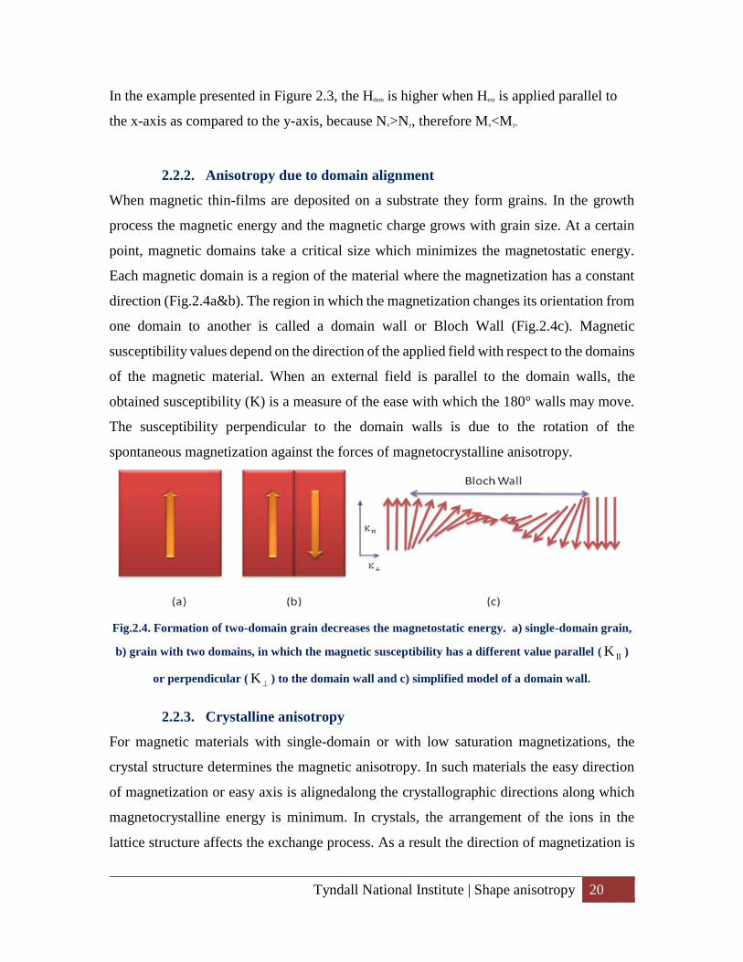
Fig.2.4. Formation of two-domain grain decreases the magnetostatic energy. a) single-
domain grain, b) grain with two domains, in which the magnetic susceptibility has a
different value parallel (IIK ) or perpendicular (
K ) to the domain wall and c) simplified
model of a domain wall…………………………………………………………………..20
Fig.2.5. The magnetocrystalline energy is highest when the system is magnetized along a
“hard” direction and lowest when magnetized along an “easy” direction. ……………...21
Fig.2.6. Schematic diagram of textural anisotropy. The arrow shows the direction of
maximum magnetic susceptibility……………………………………………………….21
Fig.2.7. Simple model of exchange anisotropy. Tc is the Curie temperature of the
ferromagneticphase and T N is the Néel temperature of the antiferromagnetic phase…..22
Fig.2.8. One dimensional nano structure gives 2 fold symmetry………………………..27
Fig.2.9. Dimensional nanostructure gives for fold symmetry…………...………………28
Fig.2.10. AFM and MFM images of a frustrated lattice……………..…………………..29
Fig.2.11. Schematic diagram of the spin configuration of an FM-AFM bilayer at different
stages……………………………………………………………………………………..32
Fig.2.12. The presence of a bump at the interface changes the relative energy
between ferromagnet orientations. The difference in energies between (a) and (b)
corresponds to the exchange bias from a single bump. (Notice that (b) is the same
as (a) with the FM reversed)…………………………………………………………......35
Fig.2.13. A representation of surface roughness as a random FM-AFM exchange at
each atomic plaquette (arrows = random direction of exchange field), with a circular
domain superimposed. A small domain size decreases random field exchange energy,
but costs domain wall energy…………………………………………………………….36
Fig.2.14. A schematic diagramme of electroplating example of Ni platting…………….41
Fig.2.15.a) Relationship between multiferroic and magnetoelectric materials. (b)
Schematic illustrating different types of coupling present in materials. Much attention has
been given to materials where electric and magnetic order is coupled. These materials are
known as magnetoelectric materials……………………………………………………..43
Tyndall National Institute | List of figures vi
Fig.2.16. (a) X-ray diffraction results from a fully epitaxial single phase BFO/SRO on
STO(001) heterostructure. (b) Low and high resolution TEM images of
BFO/SRO/STO(001) heterostructure…………………………………………………….44
Fig.2.17. Exchange anisotropy first observed by W. Meiklejohn and C. P. Bean on Co-
CoO particle at 77K after field cooled…………………………………………………...46
Fig.3.1. Schematic diagram of SHB loop tracer…………………………………………48
Fig. 3.2. Real image of SHB instrument…………………………………………………49
Fig.3.3. Output voltage vs. sample position plot, as a result of moving the sample through
the pickup coils under an applied field…………………………………………………..51
Fig.3.4. Quantum Design's MPMS Superconducting Quantum Interference Device
(SQUID) magnetometer………………………………………………………………….52
Fig.3.5. Equivalent circuit of the SQUID for magnetometer……………………………53
Fig.3.6. A typical Zero Field Cooled (ZFC) – Field Cooled (FC) – Remanence curve (a)
and magnetic hysteresis (MH) loop (b) measured in SQUID magnetometer……………54
Fig.3.5. Asylum Research: Atomic Force Microscopy…………………………….……55
Fig.3.6. Schematic diagram of TEM……………………………………………….…….57
Fig.3.7. Real image of TEM……………………………………………………….…….58
Fig.3.8. Schematic Diagram of EELS………………………………………………..…..59
Fig.3.9. Principle of SEM……………………………………………………….……….60
Fig.3.10. Schematic diagram of SEM……….…………………………….……………..61
Fig.3.11. Schismatic diagram of operating principle of X-Ray Diffraction (XRD)
mechanism……………………………………………………………………………….62
Fig.3.12. Image of PANalytical X'Pert Pro MPD X-ray Diffractometer (XRD)…….....63
Fig.3.13. A schematic diagram of the LMIS and FIB column………………………….64
Fig.3.14. Schematic illustration of the operating principle of FIB……………………...65
Fig.4.1. Normalised cubic anisotropy energy surfaces ɷc (θ,ϕ). The different shapes of the
surfaces are a reflection of the sign of K1 (O'Handley, 1999)……………………...…...67
Tyndall National Institute | List of figures vii
Fig.4.2. Schematic illustration the action of 1st term (left) which induces motion of
magnetization (M) about the effective field and 2nd term is schematic to illustrate of
damped magnetic moment (M) in the presence of magnetic field (Heff)………………...70
Fig.4.3. The effect of cell size and number of cell for a sample of sphere shape. As the
cell size is reduced the ‘model’ gives much more accurate ‘spherical’ representation and
accuracy of the simulation result is also increased………………………………………71
Fig.4.4. The memory required for OOMMF simulation as a function of the number of
discrete simulation cells in three-dimensional geometry………………………………...73
Fig.5.1. Schematic diagram of sample preparation……………………………………...77
Fig.5.2. (a) SEM image of nanohole array on PMMA on Si. (b) Gold seed layer on
patterned substrate, (c) Electroplated continuous Ni45Fe55 on nanomodulated substrate,
(d) Cross section of the nanomodulated thin film………………………………………..78
Fig.5.3. Angle dependent remanant magnetization (Mr vs. θ) measured from 3D
nanomodulated film with 400nm (a) and 200nm (b) element diameter respectively……79
Fig.5.4. Hysteresis loop measure from thin nanomodulated sample. Step like MH curve
in various temperatures shows existence of metastable dipoles throughout the temperature
range. OOMMF simulated picture of magnetization configuration…………………......80
Fig. 5.5. Schematic diagram of out of plane (a-b) and in plane (c) modulation……….82
Fig.5.6. Different symmetry formation due to pattern arrangement.MFM phase images of
dipoles……………………………………………………………………………………83
Fig.5.7. Bit map image used for OOMMF simulation…………………………………..85
Fig.5.8. (a) Cross section and top view of patterned film used for simulation. (b)
Schematic diagram of rotation of Hext in x-y plane. Uniaxial anisotropy in <100>
direction of the pattern is considered for all simulation………………………………….86
Fig.5.9. The patterned was rotated for OOMMF simulation to investigate magnetic
anisotropy………………………………………………………………………………...87
Fig.5.10. (a) NME ploted as a function of angle, (b) X & Y component of (1-NMY)
ploted……………………………………………………………………………………..88
Fig.5.11. Simulated angle dependence of magnetostatic energy in nanomodulated films
for different pattern diameter (D) from 50nm to 800nm plotted in inverse polarity…….91
Fig.5.12. For closed packed array phase shift has been observed (a). Equilateral triangular
array shows 3n-fold symmetry (b). Fitted curve (redline) for 200nm (c) and 400nm (d)
pattern with derived generalized anisotropy equation (Eqn.3). (e) Symmetry dependency
for different pattern diameters, (f) Geometry depended Demagnetization energy ……93
Tyndall National Institute | List of figures viii
Fig.5.13. (a) Ideal film and model film for OOMMF simulation. (b) Angle dependent
remanant magnetization (Mr vs. θ) measured from 3D nanomodulated film with 400nm.
(c) OOMMF simulation shows dipoles exist all over the film…………………………..98
Fig.6.1. (a) A representative bright-field TEM image of the nanocomposite (b) the SAED
patterns showing diffraction spots from both the phases……………………………….103
Fig.6.2. (a) A representative bright-field TEM image of an interface; (b) electron
diffraction spots………………………………………………………………………...104
Fig.6.3. (a) The hysteresis loop shift, signifying SEB& CEB at different temperatures
across 5-300 K. Asymmetry and tunability of the SEB depending on the sign of the
starting field (+50 kOe/-50 kOe) of hysteresis loop measurement……………………..107
Fig.6.4. The variation of exchange bias in SEB & CEB – measurements……………...108
Fig.6.5. (a) the characteristic dip at ~21 K in the differential between two ZFC
magnetization versus temperature patterns recorded under two different protocols simple
ZFC and a ZFC with ”stop-and-wait” approach. (b) the impact of training effect on CEB
for sample-A……………………………………………………………………………109
Fig.6.6. The memory effect observed at 21 K, 50 K, 100 K, and 150 K under ’stop-and-
wait’ protocol of magnetic moment versus temperature measurement. This effect proves
the presence of superspin glass moments in the nanocomposite. The effect becomes more
prominent as the temperature decreases………………………………………………...110
Fig.6.7. (a) MH curve and (b) the SEB for all the three samples with different volume
fractions of the Bi2Fe4O9 phase. (c) The CEB and HC versus temperature plot for sample B.
Large CEB (measured following field cooling under 50 kOe) could be observed at only
below TB……………………………………………………………………………...…111
Fig.6.8. The zero-field cooled (ZFC), field cooled (FC), and remanent magnetization
versus temperature plots for (a) sample-A and (b) sample-B; the solid lines show the ZFC
and FC magnetizations after subtraction of the contribution of paramagnetic C/T
component in both the cases; TB turns out to be >350 K for sample-A and ~60 K for
sample-B………………………………………………………………………………..112
Fig.6.9. Schematic of the ferromagnetic and antiferromagnetic spin interaction via
superspin glass moments at the interface……………………………………………….114
Fig.6.10. The path dependency of (a) spontaneous exchange bias and (b) corresponding
coercivity as a function of temperature; the path dependency of (c) conventional
exchange bias and (d) corresponding coercivity as a function of temperature…………117
Fig.6.11. The asymmetry in SEB and CEB -ΔHSEBand ΔHCEB- as a function of
temperature; ΔHSEB exhibits a peak around 200 K while ΔHCEBis rather monotonic across
5-300 K…………………………………………………………………………………119
Tyndall National Institute | List of figures ix
Fig.6.12. The temperature dependence of (a) conventional exchange bias and (b)
corresponding coercivity; there is an anticorrelation between HCEBand HCthroughout the
entire range of Hm and temperature; while HCEB decreases with the increase in
temperature, HCincreases……………………………………………………………….120
Fig.6.13. (a) The zero-field cooled, field-cooled, and remanent magnetization versus
temperature plots; inset shows the dM/dT vs T plots; (b) the hysteresis loop shifts at
different temperatures showing the exchange bias; the portion near the origin is blown up;
inset shows the full loops……………………………………………………………….121
Fig.6.14. The temperature dependence of (a) exchange bias and (b) coercivity and the
asymmetry of (c-d) exchange bias and coercivity across 5–100 K……………………..122
Fig.6.15. The complex ac susceptibility vs temperature plot at different frequencies; inset
shows the shift in the peak temperature with the frequency……………………………122
Fig.6.16. (a) The relaxation of the magnetization measured alternatively under +50 and
−50 kOe at 5 K; (b) field dependence of the thermo and isothermal remanence at
5K……………………………………………………………………………………….123
Fig.6.17. The hysteresis loops measured at 2 K following different protocols starting with
+50 kOe (blue line) and −50 kOe (red line); anomalous jump structures could be seen in
different branches of the loops; inset shows the spin structure…………………………125
Fig.7.1. X-ray Diffraction (XRD) pattern of the Ni50Fe50 thin film sample…………..134
Fig.7.2. High-resolution transmission electron microscopy (HRTEM) of the Ni50Fe50 thin
film image……………...…………………………………………………………….…135
Fig.7.3. Energy-dispersive X-ray spectroscopy analysis of the Ni50Fe50 thin film ……135
Fig.7.4. Selected area diffraction image of Ni3Fe rich region ………..…………….…136
Fig.7.5. Exchange bias at 300 K and 5 K………………………………………………138
Fig.7.6. Clockwise (a) and couner-clockwise (b) hysteresis loop formation. The switching
from positive to negative hysteresis loop is at 688 Oe. (c) The amount of exchange bias
decreases with increase of field range and reaches zero at 50 kOe…………………….139
Fig.7.7. (a) Clockwise hysteresis loop observation at 2K temperature. (b) No step has not
been observed throughout 50kOe loop range. (c) The hysteresis loop observed at 2K with
50kOe coincides with low field (200 Oe) measurements. (d) δM/δH has been plotted for
both positive and negative hysteresis loops…………………………………………….140
Fig.8.1. EM wave inside pattered media……………………………………………….144
Fig.8.2. Single and multilayer nanomodulated film…………………………………..146
Tyndall National Institute | List of tables x
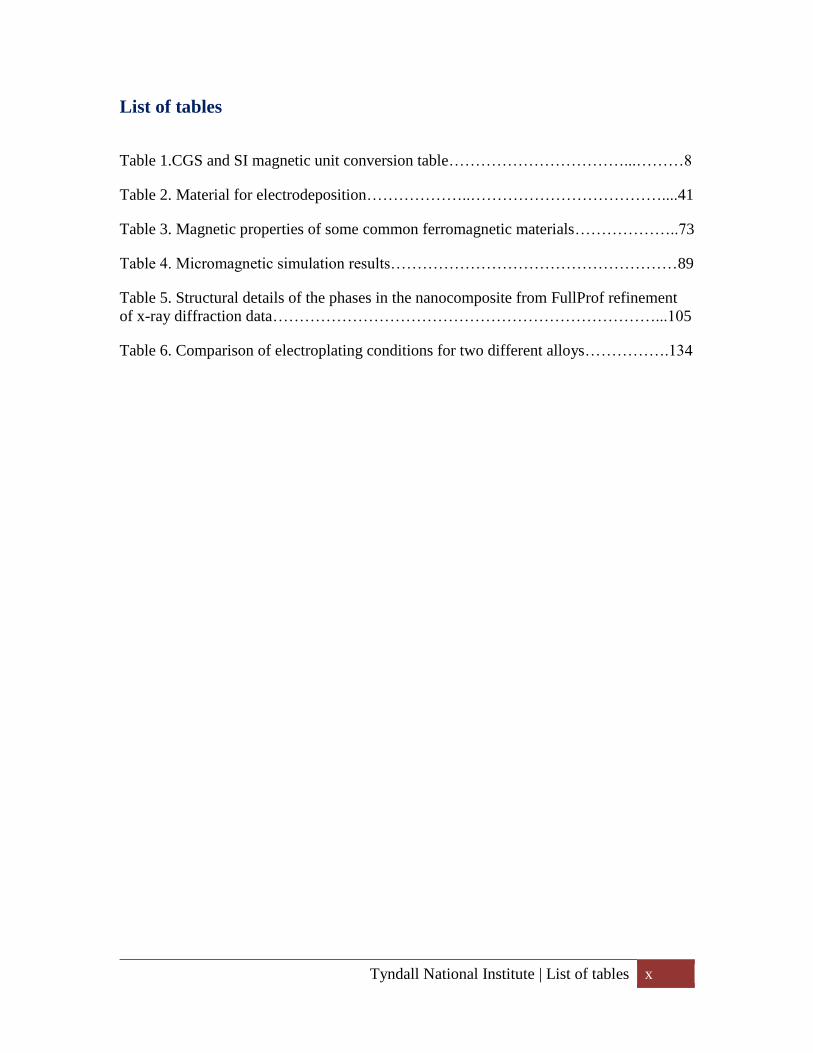
List of tables
Table 1.CGS and SI magnetic unit conversion table……………………………...………8
Table 2. Material for electrodeposition………………..………………………………....41
Table 3. Magnetic properties of some common ferromagnetic materials………………..73
Table 4. Micromagnetic simulation results………………………………………………89
Table 5. Structural details of the phases in the nanocomposite from FullProf refinement
of x-ray diffraction data………………………………………………………………...105
Table 6. Comparison of electroplating conditions for two different alloys…………….134
Tyndall National Institute | Decleration xi
Decleration
I, Tuhin Maity, declare that the thesis titled ‘Manipulation of magnetic anisotropy in
nanostructures’ and the work presented in it are my own work for the dissertation
purpose. I further confirm that:
This work was done entirely by me for a research degree at the University.
Any part of this thesis has previously not been submitted for a degree or any other
qualification at this University or any other institution, if there is any overlap that
has been clearly stated.
Where I have consulted the published work of others, is clearly attributed with
proper references.
Where I have quoted from the work of others, the source is always given.
With the exception of such quotations, this thesis is entirely my own work.
I have acknowledged all main sources of help.
Where the thesis is based on work done by myself jointly with others, I have
made clear exactly what was done by others and what I have contributed myself.
Most parts of this work have been published as several international journal
papers.
Signature
Date:
Tyndall National Institute | Abstract 1
Abstract
The magnetic properties of micro/nano-structure have attracted intense research interest in
relation to geometrically-induced magnetism to delineate fundamental magnetic
phenomena as well as focus the technological aspects in areas such as magnetic sensors,
storage devices, integrated inductive components and a number of novel magnetic devices.
Depending on the device applications, materials with high, medium or low magnetic
anisotropy and their potential manipulation are required. The elements like geometry,
crystal structure, magnetic spin configuration at the surfaces and interfaces are the basic
ingredients for this manipulation. The most dramatic manifestation in this respect is the
chance to manipulate the magnetic anisotropy over the intrinsic preferential direction of
the magnetization, commonly observed in all ferromagnetic materials, thus opening up
further possibility and functionality of ferromagnetic materials for device applications.
In this thesis various types of magnetic anisotropy of different nanostructured materials
and their manipulation are investigated. As a first approach detailed experimental and
analytical methods for the qualitative and quantitative determination of magnetic
anisotropy in nanomodulated Ni45Fe55 thin film are studied. In-plane magnetic field
rotations in modulated Ni45Fe55 revealed various rotational symmetries of magnetic
anisotropy due to dipolar interaction with a crossover from lower to higher fold as a
function of modulation geometry. The tendency to form vortex is in fact found to be very
small, which highlights that the strong coupling between metastable dipoles is more
favorable than vortex formation to minimize energy in this nanomodulated structure.
Derived mathematical expressions based on magnetic dipolar interaction and results
obtained from Object Oriented Micromagnetic Framework (OOMMF) simulation are
found to be in good agreement with our results.
Further a second approach was investigated to control exchange anisotropy mostly known
as excahneg bias at ferromagnetic (FM) – aniferomagnetic (AFM) interface in multifferoic
nanocomposite materials where two different phase/types of materials have been
simultaneously synthesized. Apart from the strong multiferroic coupling at room
temperature, BiFeO3, with a long wavelength (~62 nm) cycloidal magnetic structure and
Tyndall National Institute | Abstract 2
canted antiferromagnetism, exhibits an additional functionality of switching the magnetic
anisotropy of a ferromagnetic layer via exchange bias coupling in a BiFeO3
antiferromagnetic – Bi2Fe4O9 ferromagnetic layer composite. The switching can be
triggered both by a magnetic as well as an electric field because of strong multiferroicity.
Magnetic field, temperature and measurement protocol dependence of magnetic anisotropy
of nanoscale multiferroic materials are presented.
The third parallel aspect of this work was to electroplate thin films of metal alloy
nanocomposite for enhanced exchange anisotropy. In this work an unique observation of
positive (anti clock wise) and negative (clock wise) hysteresis loop formation in the Ni,Fe
solid solution with very low coercivity and large positive exchange anisotropy/exchange
bias are investigated. These two opposite (positive/negative) hysteresis loop formation
occur depending upon the field range used in hysteresis loop measurement and thus can
potentially be manipulated. Hence, controllable positive and negative exchange bias is
observed which has high potential application such as in MRAM devices.
In this thesis, the current state of the art has been described in chapter one. In chapter two
a broad literature review on the area of research has been reviewed.
Different experimental techniques used in this work are discussed in details in chapter
three.
Micromagnetic simulation has been carried out to understand further the mechanism of
magnetic materials. This has been discussed in chapter four.
In chapter five the magnetic anisotropy control by 3D nanomodulation including how to
avoid vortex formation in a continuous film are discussed.
Chapter six introduces giant exchange anisotropy in multiferroic nanocomposite (BiFeO3-
Bi2Fe4O9) including the effect of temperature and magnetic field on it.

Tyndall National Institute | Abstract 3
Chapter seven examines how the exchange anisotropy can be used to manipulate hysteresis
loop direction in alloy composites with low coercivity (HC).
Chapter eight concludes with the summary of the key findings of the study, potential
application of them and possible future scope of the present research.
Tyndall National Institute | List of Publications 4
List of Publications
Journal Papers
Published in 2015
1. Reply to the comment on “Superspin glass mediated giant spontaneous exchange
bias in a nanocomposite of BiFeO3-Bi2Fe4O9”
Tuhin Maity, Sudipta Goswami, Dipten Bhattacharya, and Saibal Roy
Physical Review Letter 114 (9), 099704 (2015)
Published in 2014
2. “Large Magnetoelectric Coupling in Nanoscale BiFeO3 from Direct Electrical
Measurements”
Sudipta Goswami, Dipten Bhattacharya, Lynette Keeney, Tuhin Maity, S.D. Kaushik, V.
Siruguri, Gopes C. Das, Haifang Yang, Wuxia Li, C.-Z. Gu, M.E. Pemble, and Saibal
Roy
Physical Review B 90 (10), 104402 (2014)
3. “Origin of the asymmetric exchange bias in BiFeO3/Bi2Fe4O9 nanocomposite”
Tuhin Maity, Sudipta Goswami, Dipten Bhattacharya, and Saibal Roy
Physical Review B 89 (14), 1404112014 (2014)
Published in 2013
4. “Size and space controlled hexagonal arrays of superparamagnetic iron oxide
nanodots: magnetic studies and application”
T Ghoshal, T Maity, R Senthamaraikannan, MT Shaw, P Carolan, Justin D Holmes,
Saibal Roy, Michael A Morris
Scientific Reports 3, 2013
5. “Magnetic Field‐Induced Ferroelectric Switching in Multiferroic Aurivillius
Phase Thin Films at Room Temperature”
L Keeney, T Maity, M Schmidt, A Amann, N Deepak, N Petkov, S Roy, Martyn E
Pemble, Roger W Whatmore
Journal of the American Ceramic Society 96 (8), 2339-2357, 2013 (Feature article)
6. ‘’Superspin glass mediated giant spontaneous exchange bias in a nanocomposite
of BiFeO3- Bi2Fe4O9’’
T Maity, S Goswami, D Bhattacharya, S Roy
Physical Review Letter 110, 107201 (2013)
Tyndall National Institute | Journal Papers 5
7. ‘’Spontaneous exchange bias in a nanocomposite of BiFeO3-Bi2Fe4O9’’
T Maity, S Goswami, G C Das, D Bhattacharya, S Roy
Journal of Applied Physics 113, (2013)
Published in 2012
8. ‘’Ordered magnetic dipoles: Controlling anisotropy in nanomodulated continuous
ferromagnetic films’’
Tuhin Maity, Shunpu Li, Lynette Keeney, Saibal Roy,
Physical Review B 86 (024438), 7(2012)
9. ‘’Large Scale Monodisperse Hexagonal Arrays of Superparamagnetic Iron Oxides
Nanodots: A Facile Block Copolymer Inclusion Method’’
T Ghoshal, T Maity, JF Godsell, S Roy, MA Morris
Advanced Materials 5 (2012)
Book Chapters:
10. “Nanostructured Magnetic Materials for High-Frequency Applications - Beyond-
CMOS Nanodevices 1, 457-483”
S. Roy, J. Godsell and T. Maity
Wiley Publication 2014
11. “Novel approaches for genuine single phase room temperature magnetoelectric
multiferroics”
Lynette Keeney, Michael Schmidt, Andreas Amann, Tuhin Maity, Nitin Deepak, Ahmad
Faraz, Nikolay Petkov, Saibal Roy, Martyn E. Pemble and Roger W. Whatmore
Wiley Publication 2014 (In press)
Journal papers from Master’s Programme (from previous Institutes)
Published in 2012
12. ‘’Structural, magnetic and electric properties of HoMnO3 films on SrTiO3(001)’’
R Wunderlich, C Chiliotte, G Bridoux, T Maity, Ö Kocabiyik, A Setzer, M .
Journal of Magnetism and Magnetic Materials 324 (4), 460-465(2012)
13. ‘’Observation of Enhanced Dielectric Coupling and Room Temperature
Ferromagnetism in Chemically Synthesized BiFeO3@ SiO2 Core–shell Particles’’
MM Shirolkar, R Das, T Maity, P Poddar, SK Kulkarni
The Journal of Physical Chemistry C1(2012)
Tyndall National Institute | Journal Papers 6
Published 2011
14. ‘’Dielectric and spin relaxation behaviour in DyFeO3 nanocrystals’’
A Jaiswal, R Das, T Maity, P Poddar
Journal of Applied Physics 110 (12), 124301-124301-7(2011)
Published in 2010
15. ‘’Investigations of magnetic and dielectric properties of cupric oxide
nanoparticles’’
RS Bhalerao-Panajkar, MM Shirolkar, R Das, T Maity, P Poddar, SK Kulkarni
Solid State Communications 5(2010)
16. ‘’Temperature-Dependent Raman and Dielectric Spectroscopy of BiFeO3
Nanoparticles: Signatures of Spin-Phonon and Magnetoelectric Coupling’’
A Jaiswal, R Das, T Maity, K Vivekanand, S Adyanthaya, P Poddar
The Journal of Physical Chemistry C 9(2010)
17. ‘’Magnetic and dielectric properties and Raman spectroscopy of GdCrO3
nanoparticles’’
A Jaiswal, R Das, K Vivekanand, T Maity, PM Abraham, S Adyanthaya, P Poddar
Journal of Applied Physics 107 (1), 013912-013912-7 11(2010)
International Peer Reviewed Conference Proceedings
Presented in 2013
18. Super spin mediated giant exchange bias in multiferroic nanocomposite
Tuhin Maity, Sudipta Goswami, Dipten Bhattacharya and Saibal Roy
JEMS 2014, Rhodos, Greece
19. ‘’Observation of tunable magnetic dipoles by MFM in nanomodulated continuous
ferromagnetic film’’
Tuhin Maity, Saibal Roy
IEEE MMM/Intermag 2013, Chicago, 2013
20. ‘’Synthesis and Multiferroic Investigations of Bi7Ti3Fe2.1Mn0.9O15 Aurivillius
Phase Thin Films’’
Lynette Keeney, Tuhin Maity, Michael Schmidt, Nitin Deepak, Saibal Roy, Martyn E.
Pemble, Roger W. Whatmore, COST MPO904 Action / IEEE-ROMSC Iasi, Romania, 24
Sept 2012.
Tyndall National Institute | Journal Papers 7
21. ‘’Synthesis and Multiferroic Investigations of Bi m+1Ti3Fe m-3O 3m+1 Aurivillius
Phase Thin Films where m ≥ 6’’
Lynette Keeney, Tuhin Maity, Michael Schmidt, Nitin Deepak, Saibal Roy, Martyn E.
Pemble, Roger W. Whatmore, ISAF-ECAPD-PFM- 2012 – Aveiro, Portugal, 11 July
2012.
22. ‘’Multiferroic (ferroelectric/ferromagnetic) behaviour of Aurivillius Phase Thin
Films’’
Roger W. Whatmore, Lynette Keeney, Tuhin Maity, Michael Schmidt, Nitin Deepak,
Saibal Roy, Andreas Amann, Nikolay Petkov, Martyn E. Pemble, Electronic Materials
and Applications 2013, January 23 - 25, 2013, Orlando, Florida
Presented in 2012
23. ‘’A facile block copolymer inclusion technique for large scale monodisperse
hexagonal arrays of superparamagnetic iron oxides nanodots’’
T Ghoshal, T Maity, JF Godsell, S Roy, MA Morris Nanotechnology 2012 1, 128 -
131(2012) ISBN:978-1-4665-6274-5 CRC Press Taylor & Francis
24. ‘’Symmetry of magnetic dipole controlled anisotropy in nanomodulated thin
ferromagnetic film’’
Tuhin Maity, Shunpu Li, Saibal Roy
IEEE INTERMAG 2012, Vancuver, Canada
25. ‘’Symmetry of magnetic anisotropy in 3D nanomodulated continuous thin
ferromagnetic film’’
Tuhin Maity, Shunpu Li, Saibal Roy
ICSM 2012, Istanbul, Turkey
Presented in 2011
26. ‘’Symmetry of magnetic anisotropy in nanomodulated thin ferromagnetic film’’
Tuhin Maity, Shunpu Li, Saibal Roy
Syncroton User Meeting 2011, Oxford, UK
Tyndall National Institute | Units 8
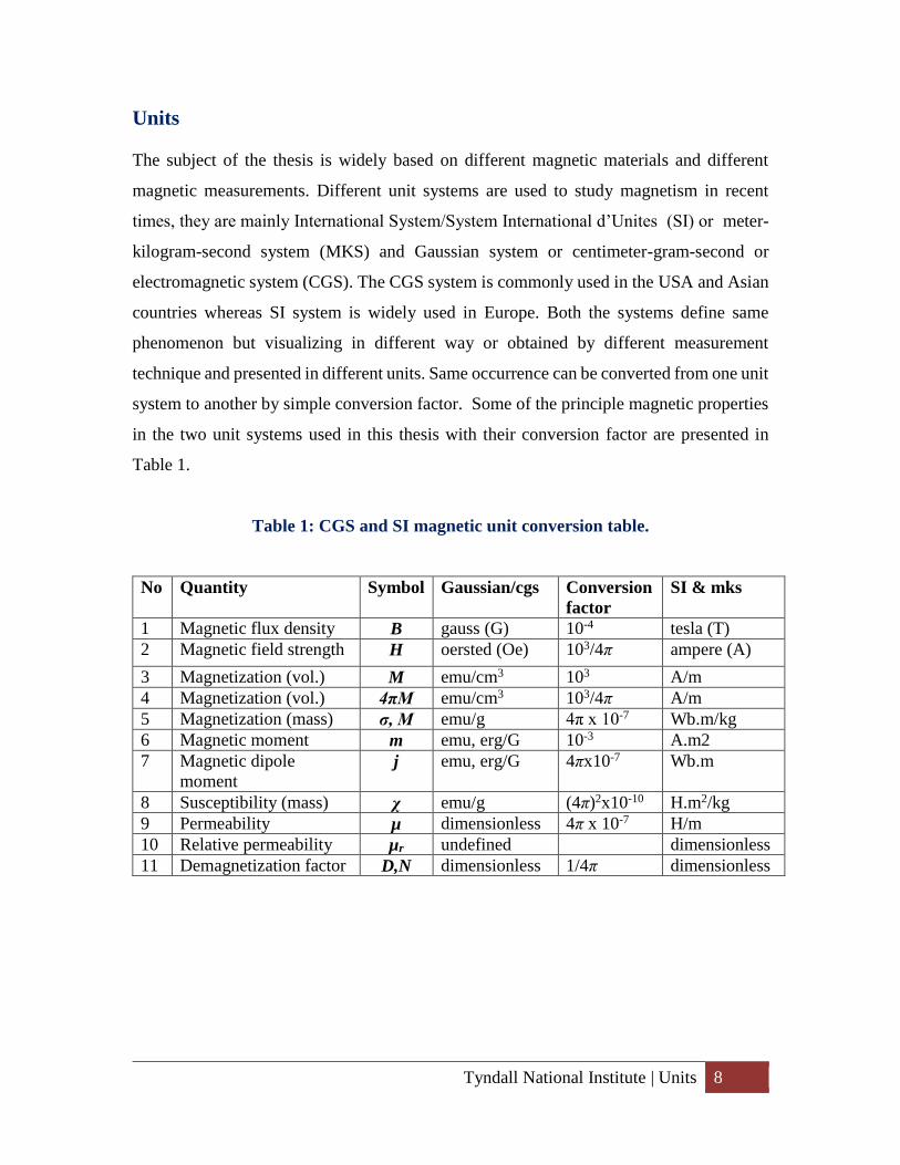
Units
The subject of the thesis is widely based on different magnetic materials and different
magnetic measurements. Different unit systems are used to study magnetism in recent
times, they are mainly International System/System International d’Unites (SI) or meter-
kilogram-second system (MKS) and Gaussian system or centimeter-gram-second or
electromagnetic system (CGS). The CGS system is commonly used in the USA and Asian
countries whereas SI system is widely used in Europe. Both the systems define same
phenomenon but visualizing in different way or obtained by different measurement
technique and presented in different units. Same occurrence can be converted from one unit
system to another by simple conversion factor. Some of the principle magnetic properties
in the two unit systems used in this thesis with their conversion factor are presented in
Table 1.
Table 1: CGS and SI magnetic unit conversion table.
No Quantity Symbol Gaussian/cgs Conversion
factor
SI & mks
1 Magnetic flux density B gauss (G) 10-4 tesla (T)
2 Magnetic field strength H oersted (Oe) 103/4π ampere (A)
3 Magnetization (vol.) M emu/cm3 103 A/m
4 Magnetization (vol.) 4πM emu/cm3 103/4π A/m
5 Magnetization (mass) σ, M emu/g 4π x 10-7 Wb.m/kg
6 Magnetic moment m emu, erg/G 10-3 A.m2
7 Magnetic dipole
moment j emu, erg/G 4πx10-7 Wb.m
8 Susceptibility (mass) χ emu/g (4π)2x10⁻¹⁰ H.m2/kg
9 Permeability µ dimensionless 4π x 10-7 H/m
10 Relative permeability µr undefined dimensionless
11 Demagnetization factor D,N dimensionless 1/4π dimensionless
Tyndall National Institute | Chapter – Introduction 9
1. Chapter – Introduction
1.1. Background
The magnetic properties of micro/nano-structured materials have attracted intense research
interest from the viewpoints of geometrically-induced magnetism to delinate fundamental
magnetic phenomena and also from the technological point of view in areas such as
magnetic sensors, storage devices, integrated inductive components and a number of
magnetic devices for novel applications. It is a well-known experimental fact that
ferromagnetic material exhibits ‘easy’ and ‘hard’ directions of the magnetization
depending on magnetic spin configuration for energy minimization. For the technological
application this magnetic anisotropy becomes one of the most important properties of
magnetic materials. The enormous research on magnetic properties of nanostructures has
been the thrust in recent years behind the fundamental understanding of the magnetic
anisotropy and its application in micromagnetic devices. For advanced device applications,
materials with tuneable anisotropy are more useful.
A preferred magnetic moment orientation in nanostructured material can be quite different
in terms of the factors that account for the easy-axis alignment in bulk material, and
consequently the anisotropy strength can also be significantly different. The influence of
the elements like geometry, crystal structure, magnetic spin configuration at the materials
interfaces and surfaces, are the basic ingredients for this behavior. By varying the suitable
parameters and choosing appropriate materials, it is possible to tailor the magnetic
anisotropy. The most dramatic manifestation in this respect could be the chance to
manipulate the magnetic anisotropy over the intrinsic preferential direction of the
magnetization as commonly observed in all ferromagnetic thin films which can open up
new window of functionality of ferromagnetic materials for device applications.
Different type of magnetic anisotropy of magnetic nanostructured thin films and their
manipulation is discussed in this thesis. Magnetocrystalline, dipolar (shape),
magnetoelastic and exchange anisotropies are explained. Detailed experimental and
analytical methods for the quantitative and qualitative determination of various magnetic
anisotropies are described. Many experimental results are further investigated by Object
Oriented Micromagnetic Framework (OOMMF) simulation. Magnetic field, temperature
Tyndall National Institute | Motivation of the work 10
and measurement protocol dependence of magnetic anisotropy of nanoscale materials are
presented. It is shown that geometry of nanostructures, material interface and selection of
materials play important role to determine the magnetic anisotropy.
1.2. Motivation of the work
The interest in nanostructured magnetic materials has experienced a tremendous boost for
potential use in numerous present and future device applications such as sensors, actuators,
magnetic data storage and integrated passive devices due to the tunable magnetic properties
and simultaneous improvement in material preparation technique. Following the
unavoidable trend of device miniaturization, the present research trend is focused on
various ways to reduce the size of every aspect of integrated circuits and integrated
magnetic components. In all such applications the key property of ferromagnetic materials
is the direction of its magnetization which is widely based on magnetic anisotropy. This is
the property which determines the preferred easy or hard magnetization directions of
magnetic domains at remanence state and also decides the magnetization reversal process
in presence of external field.
1.3. Defining the scope of the Thesis
A number of novel magnetic materials have been investigated to find out new possibilities
to control and enhance magnetic anisotropy for next generation device applications. A
unique nanopatterned soft magnetic thin film was investigated for possible magnetic
anisotropy (shape/dipole) control. The goal of the work is to investigate a unique low cost
solution to control magnetic anisotropy for device applications.
The magnetic anisotropy has been distinguished depending on its origin. The crystalline
anisotropy or magnetoelastic anisotropy is intrinsic in nature and originates due to spin–
orbit coupling (SOC) depending on crystalline structure of the materials. For
polycrystalline materials, the overall magnetic anisotropy is of dipolar origin and largely
Tyndall National Institute | Defining the scope of the Thesis 11
originates from the shape and known as shape anisotropy. In the present desertation work
magnetic anisotropy of polycrystalline nanomodulated Ni45Fe55 films have been studied as
a function of modulation geometry. In plane magnetic field rotations revealed a rotational
symmetry of magnetization in a unique nanomodulated structure. We found a systematic
crossover from lower folds to higher folds of magnetic symmetry in nanomodulated
continuous film depending upon the modulation parameters. It is argued that this complex
rotational symmetry can be introduced and controlled by proper 3-dimentional modulation
having a particular geometrical symmetry. Analytical expression for the angular
dependence of the magnetization was obtained to validate the experimental results. The
overall discussion is focused on the effect of 3-dimensional geometry on magnetic property
of a ferromagnetic thin film. The nanomodulation technique used in this work is cost
effective. A further investigation in this work was how to avoid magnetic vortex formation
in nano-patterned ferromagnetic material. The existence of both in plane and out of plane
dipoles in this 3D nanomodulation film and their competition resulting into a metastable
state don’t allow vortex formation (the minimum energy state). This is an essential
requirement for nanostrcutured ferromagnetic materials in memory device application.
A second approach in a novel technique was employed to control exchange anisotropy
mostly known as exchange bias at ferromagnetic (FM) – aniferomagnetic (AFM) interface
showing for the first time its tuneability in multiferroic nanocomposite materials where two
different phase/types of materials can be simultaneously synthesized. Apart from the strong
multiferroic coupling at room temperature, BiFeO3, with a long wavelength (~62 nm)
cycloidal magnetic structure and canted antiferromagnetism, exhibits an additional
functionality of switching the magnetic anisotropy of a ferromagnetic layer via exchange
bias coupling in a BiFeO3 antiferromagnetic – Bi2Fe4O9 ferromagnetic layer composite.
We have shown that the switching can be triggered both by a magnetic as well as an electric
field because of strong multiferroicity present in the system. The role of exchange bias
coupling has been noted not just in a single crystal BiFeO3-ferromagnetic layer system but
in other thin film based heterostructures as well. Whether the exchange bias is larger in thin
film or in bulk BiFeO3 based bilayer systems is debatable. While the exchange bias in thin
films and nanoscale systems originates from uncompensated cycloid of the magnetic
Tyndall National Institute | Summary and Thesis Layout 12
structure, larger canting angle offers significant exchange bias even in bulk BiFeO3 based
systems.
The third parallel aspect of this work was to study the electroplated thin films of metal
alloy nanocomposite for enhanced exchange bias. In this work we described direct
observation of positive (anti clock wise) and negative (clock wise) hysteresis loop
formation in the Ni,Fe solid solution with very low coercivity and large positive exchange
anisotropy/exchange bias. These two opposite (positive/negative) hysteresis loop
originated depending upon the field range of hysteresis loop measurement. Like most other
positive exchange bias system Ni45Fe55 shows positive shift at field direction when the loop
tracing field range is relatively small (just above the saturation field) and the loop is
positive. However, when the film is measured with a higher loop tracing field range, we
observed a typical negative hysteresis loop with no exchange bias. The main interest here
was to achieve high exchange bias for materials with very low coercivity and low saturation
magnetic field and trigger the hysteresis loop direction. The importance of this study lays
in the essence on high exchange anisotropic materials for cutting edge technologies.
1.4. Summary and Thesis Layout
In this thesis at first the current state of the art in chapter two a broad literature review of
the area of research has been reviewed. In chapter three different experimental techniques
used in the work are discussed in details. Micromagnetic simulation has been performed to
understand further the mechanism of magnetic materials. This has been introduced in
chapter four. In chapter five, the magnetic anisotropy control by 3D nanomodulation and
how to avoid vortex formation are discussed. Chapter six introduces giant exchange bias
in multiferroic nanocomposite (BiFeO3-Bi2Fe4O9) and the effect of temperature and
magnetic field on it. Chapter seven examines how the exchange bias can be used to
manipulated hysteresis loop direction in alloy composite with low coercivity (HC). Chapter
eight concludes with the summary of the key findings of the study, potential applications
of them and possible future scope of the research.
Tyndall National Institute | Chapter – State of the Art Review 13
2. Chapter – State of the Art Review
2.1. Introduction
In this chapter the state of the art in current research on magnetic anisotropy control in
different ferromagnetic materials is discussed. Magnetic anisotropy in general is a
fundamental property of magnetic materials. The magnetization tends to lie in a preferred
direction to obtain lowest magneto-static energy state. The energy includes an anisotropy
term Ea(θ,φ) where the direction of magnetization is defined by the angular coordinates θ
and φ. The anisotropy can be intrinsic, related to atomic scale interactions in a unit cell
which define easy directions in the crystal structure called magnetocrystalline anisotropy.
It can also be related to the energy of the sample in its own demagnetizing field due to the
sample geometry called shape/dipolar anisotropy. Exchange bias or exchange anisotropy
occurs due to magnetic interaction between layers of magnetic materials where the strong
magnetic coupling of an antiferromagnetic thin film causes a shift in the magnetic loop of
soft magnetization of a ferromagnetic film. Magnetic anisotropy is one of the very
important parameters in relation to the characterization of materials which is widely used
in different technological applications, particularly magnetic recording media, sensors,
magnetic passive devises, etc. The enormous research on magnetic anisotropy of ultrathin
films and nanostructures opens up new horizon in terms of fundamental understanding as
well. This chapter includes fundamental theory of different magnetic anisotropy and recent
developments in this field.
A vast number of magnetic devices are employed in the present day electronic industry. In
ancient time the magnetic phenomenon in human beings were experienced by utilizing
natural iron minerals. In modern times this was understood and explained from the
standpoint of electromagnetics, to which many physicists such as Oersted and Faraday
made a great contribution. In 1822 Ampère explained magnetic materials based on a small
circular electric current which was the first explanation of a molecular magnet. Later,
Ampère’s circuital law introduced the concept of a magnetic moment or magnetic dipoles.
The magnetic field generated by an electrical field is given by Ampère’s circuital law as
∮ 𝐻. 𝑑𝑙 = 𝐼
Tyndall National Institute | Introduction 14
Where the total current (I), is equal to the line integral of the magnetic field (H) around a
closed path containing the current. Whereas, in the materials the origins of the magnetic
moment and it’s magnetic field are the electrons in atoms comprising the materials. The
response of materials to an external magnetic field is relevant to magnetic energy
expressed as (in CGS)
𝐸 = −𝑚. 𝐻
In SI unit
𝐸 = −µ0𝑚. 𝐻
where µ0 is the magnetic permeability of free space.
The magnetization M is a property of the material which depends on the individual
magnetic moments of its constituent magnetic origins. The magnetization of the material
reflects the magnetic interaction at a microscopic molecular level which results in
experimental behaviors due to external parameters such as temperature and magnetic field.
Magnetic induction (B) is a magnetic response of the material when it is placed in an
external magnetic field (H). The relationship between B and H is expressed as (in CGS)
𝐵 = 𝐻 + 4𝜋𝑀
In SI units the relationship is given using the permeability of free space (𝜇0) as
𝐵 = 𝜇0(𝐻 + 𝑀)
The magnetic properties are measured as a direct magnetization response to the applied
magnetic field and the ratio of M to H expressed by magnetic susceptibility χ.
𝜒 = 𝑀/𝐻
The magnetization M of ordinary materials exhibits a linear function M = χ H with external
magnetic field H. Material shows either positive or negative magnetic susceptibility, i.e. χ
> 0 or χ < 0. In the case of χ > 0 the material is called as Paramagnetic and in the case of χ
< 0 it’s known as diamagnetic material. In the M – H curve this behavior is discriminated
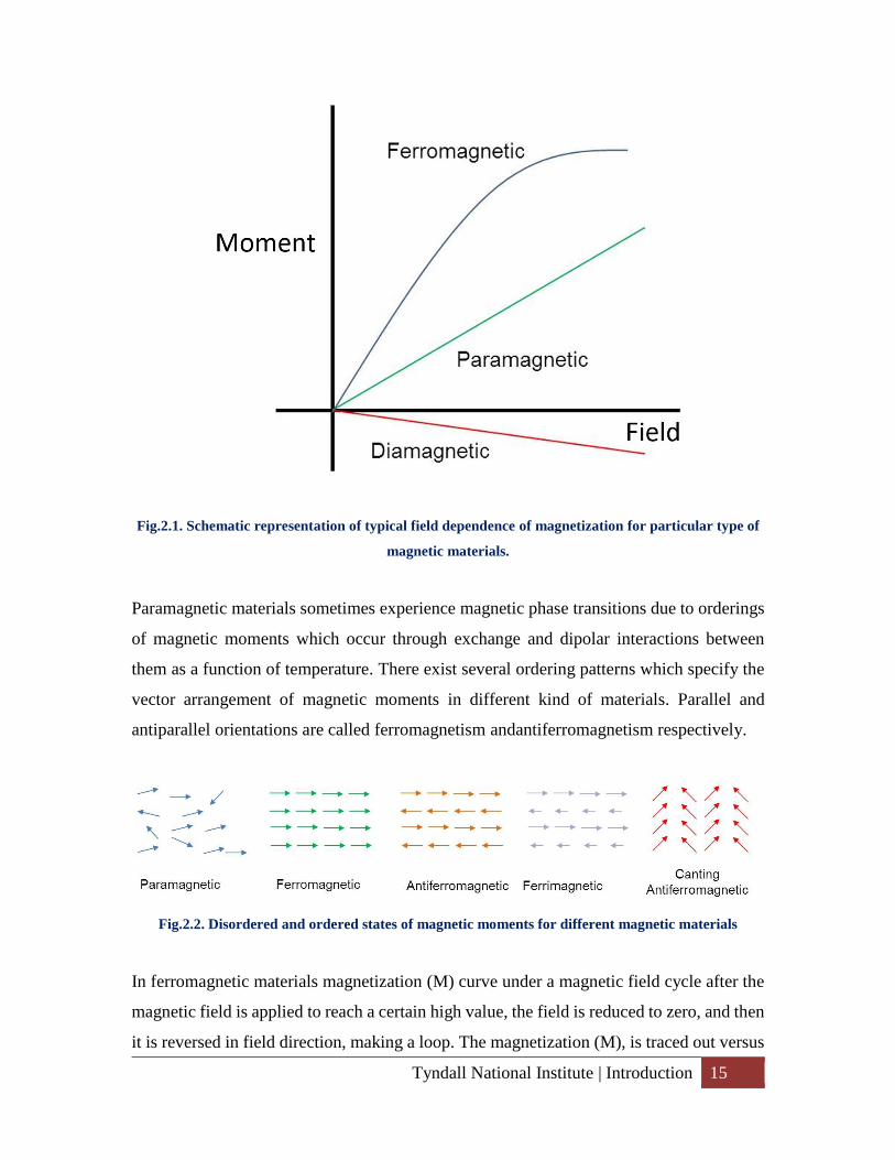
as a positive or negative MH slope, as shown in Figure 2.1. Usually, a diamagnetic response
toward an external magnetic field is very minor and the slope is very small compared to
the slope of paramagnetic material.
Tyndall National Institute | Introduction 15
Fig.2.1. Schematic representation of typical field dependence of magnetization for particular type of
magnetic materials.
Paramagnetic materials sometimes experience magnetic phase transitions due to orderings
of magnetic moments which occur through exchange and dipolar interactions between
them as a function of temperature. There exist several ordering patterns which specify the
vector arrangement of magnetic moments in different kind of materials. Parallel and
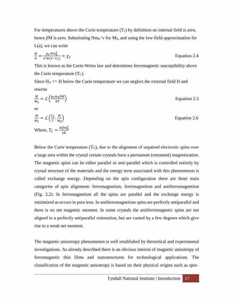
antiparallel orientations are called ferromagnetism andantiferromagnetism respectively.
Fig.2.2. Disordered and ordered states of magnetic moments for different magnetic materials
In ferromagnetic materials magnetization (M) curve under a magnetic field cycle after the
magnetic field is applied to reach a certain high value, the field is reduced to zero, and then
it is reversed in field direction, making a loop. The magnetization (M), is traced out versus
Tyndall National Institute | Introduction 16
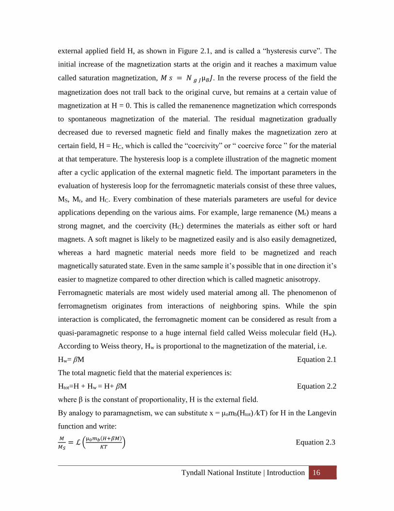
external applied field H, as shown in Figure 2.1, and is called a “hysteresis curve”. The
initial increase of the magnetization starts at the origin and it reaches a maximum value
called saturation magnetization, 𝑀 𝑠 = 𝑁 𝑔 𝐽µ𝐵𝐽. In the reverse process of the field the
magnetization does not trall back to the original curve, but remains at a certain value of
magnetization at H = 0. This is called the remanenence magnetization which corresponds
to spontaneous magnetization of the material. The residual magnetization gradually
decreased due to reversed magnetic field and finally makes the magnetization zero at
certain field, H = HC, which is called the “coercivity” or “ coercive force ” for the material
at that temperature. The hysteresis loop is a complete illustration of the magnetic moment
after a cyclic application of the external magnetic field. The important parameters in the
evaluation of hysteresis loop for the ferromagnetic materials consist of these three values,
MS, Mr, and HC. Every combination of these materials parameters are useful for device
applications depending on the various aims. For example, large remanence (Mr) means a
strong magnet, and the coercivity (HC) determines the materials as either soft or hard
magnets. A soft magnet is likely to be magnetized easily and is also easily demagnetized,
whereas a hard magnetic material needs more field to be magnetized and reach
magnetically saturated state. Even in the same sample it’s possible that in one direction it’s
easier to magnetize compared to other direction which is called magnetic anisotropy.
Ferromagnetic materials are most widely used material among all. The phenomenon of
ferromagnetism originates from interactions of neighboring spins. While the spin
interaction is complicated, the ferromagnetic moment can be considered as result from a
quasi-paramagnetic response to a huge internal field called Weiss molecular field (Hw).
According to Weiss theory, Hw is proportional to the magnetization of the material, i.e.
Hw= βM Equation 2.1
The total magnetic field that the material experiences is:
Htot=H + Hw = H+ βM Equation 2.2
where β is the constant of proportionality, H is the external field.
By analogy to paramagnetism, we can substitute x = μomb(Htot) ∕kT) for H in the Langevin
function and write:
𝑀
𝑀𝑆= ℒ (
µ0𝑚𝑏(𝐻+𝛽𝑀)
𝐾𝑇) Equation 2.3
Tyndall National Institute | Introduction 17
For temperatures above the Curie temperature (Tc) by definition no internal field is zero,
hence βM is zero. Substituting Nmb ∕ v for MS, and using the low-field approximation for
L(a), we can write
𝑀
𝐻=
µ0 𝑁𝑚𝑏2
𝑣3𝐾(𝑇−𝑇𝐶)= 𝜒𝑓 Equation 2.4
This is known as the Curie-Weiss law and determines ferromagnetic susceptibility above
the Curie temperature (TC).
Since Hw >> H below the Curie temperature we can neglect the external field H and
rewrite
𝑀
𝑀𝑆= ℒ (
µ0𝑚𝑏𝐵𝑀
𝐾𝑇) Equation 2.5
or
𝑀
𝑀𝑆= ℒ (
𝑇𝐶
𝑇.
𝑀
𝑀𝑆) Equation 2.6
Where, 𝑇𝐶 =𝑁𝛽𝑚𝑏
2
𝑣𝐾
Below the Curie temperature (TC), due to the alignment of unpaired electronic spins over
a large area within the crystal certain crystals have a permanent (remanent) magnetization.
The magnetic spins can be either parallel or anti-parallel which is controlled entirely by
crystal structure of the materials and the energy term associated with this phenomenon is
called exchange energy. Depending on the spin configuration there are three main
categories of spin alignment: ferromagnetism, ferrimagnetism and antiferromagnetism
(Fig. 2.2). In ferromagnetism all the spins are parallel and the exchange energy is
minimized as occurs in pure iron. In antiferromagnetism spins are perfectly antiparallel and
there is no net magnetic moment. In some crystals the antiferromagnetic spins are not
aligned in a perfectly antiparallel orientation, but are canted by a few degrees which give
rise to a weak net moment.
The magnetic anisotropy phenomenon is well established by theoretical and experimental
investigations. As already described there is an obvious interest of magnetic anisotropy of
ferromagnetic thin films and nanostructures for technological applications. The
classification of the magnetic anisotropy is based on their physical origins such as spin–
Tyndall National Institute | Types of magnetic anisotropy 18
orbit coupling (SOC), dipolar magnetic interaction, and exchange interaction. Based on
that, magnetic anisotropy is classified in to magnetocrystalline, magnetoelastic,
dipolar/shape, exchange, dipolar crystalline, etc. The dipolar crystalline anisotropy can be
neglected due to its small magnitude. Magnetocrystalline anisotropy, magnetoelastic
anisotropy, and shape anisotropy have been thoroughly investigated on bulk magnetism,
ultrathin film magnetism, and for different magnetic nanostructures within last few
decades. In the following sections, an overview of the electronic origin of different kind
of magnetic anisotropy is briefly discussed. The shape/dipolar magnetic anisotropy in
nanomodulated films and exchange bias in different nanostructures are introduced, and the
recent research trend in relation to that has been addressed. A comprehensive literature
review has been carried out to identify different methods to control magnetic anisotropy of
different magnetic materials. Different techniques to control anisotropy reported for the
various structured materials have been overviewed, highlighting the respective advantages
and disadvantages of each of the techniques. Examples of the techniques employed include
patterned, isolated magnetic structures and structured continuous magnetic films. These
approaches have certain limitations which inhibit their use for device applications. For
example, why the isolated nanostructure forms vortex at frustrated state and one
dimensional structure doesn’t have much control over anisotropy, etc alongwith some
potential solutions have been discussed below.
2.2. Types of magnetic anisotropy
Magnetic anisotropy has historically been analyzed by means of the anisotropy of
susceptibility and the anisotropy of an artificial remanent magnetization. Both types are
due to a non-isotropic distribution of magnetic grains. Six mechanisms have been proposed
to explain magnetic anisotropy, whereby shape anisotropy and crystalline anisotropy are
the most important ones.
2.2.1. Shape anisotropy
One of the important sources of magnetic anisotropy is shape. To understand how the shape
controls magnetic energy of the material, the concept of the internal demagnetizing field
of a magnetized body needs to be understood. The magnetic vectors within a ferromagnetic
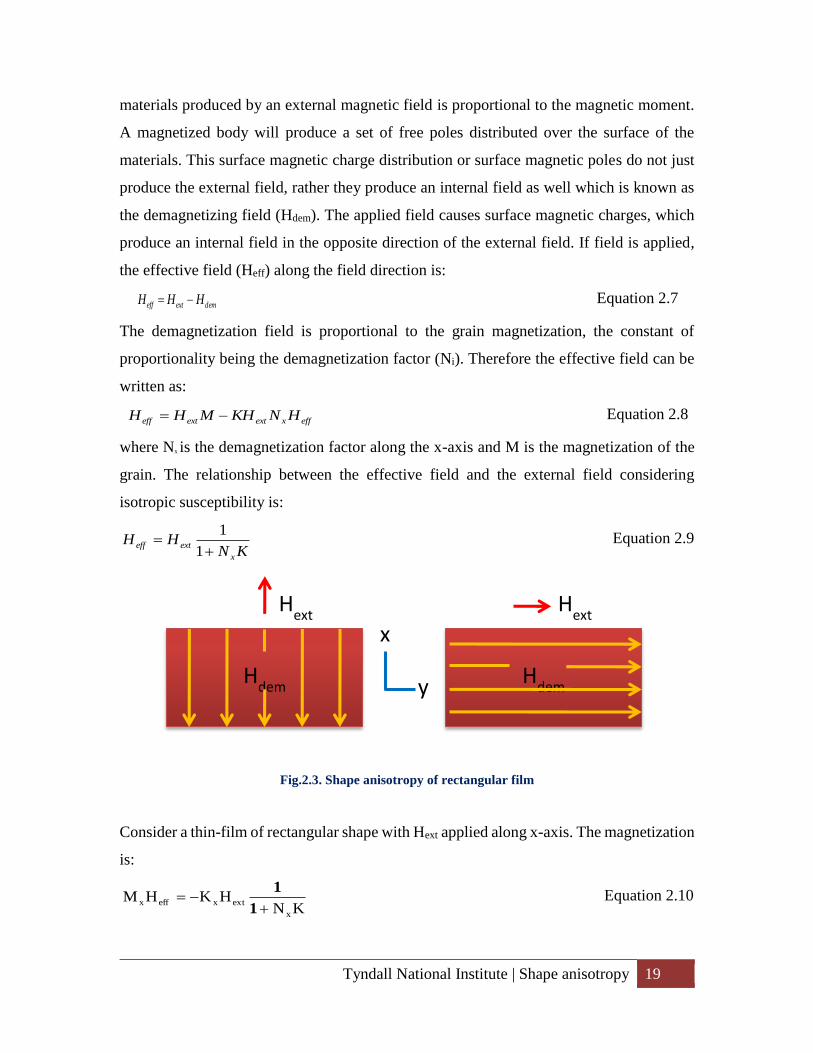
Tyndall National Institute | Shape anisotropy 19
materials produced by an external magnetic field is proportional to the magnetic moment.
A magnetized body will produce a set of free poles distributed over the surface of the
materials. This surface magnetic charge distribution or surface magnetic poles do not just
produce the external field, rather they produce an internal field as well which is known as
the demagnetizing field (Hdem). The applied field causes surface magnetic charges, which
produce an internal field in the opposite direction of the external field. If field is applied,
the effective field (Heff) along the field direction is:
demexteff HHH Equation 2.7
The demagnetization field is proportional to the grain magnetization, the constant of
proportionality being the demagnetization factor (Ni). Therefore the effective field can be
written as:
effxextexteff HNKHMHH Equation 2.8
where Nx is the demagnetization factor along the x-axis and M is the magnetization of the
grain. The relationship between the effective field and the external field considering
isotropic susceptibility is:
KNHH
x
exteff
1
1 Equation 2.9
Fig.2.3. Shape anisotropy of rectangular film
Consider a thin-film of rectangular shape with Hext applied along x-axis. The magnetization
is:
KNHKHM
x
extxeffx
1
1 Equation 2.10
Hdem
Hext
Hdem
Hext
x
y
Tyndall National Institute | Shape anisotropy 20
In the example presented in Figure 2.3, the Hdem is higher when Hext is applied parallel to
the x-axis as compared to the y-axis, because Nx>Ny, therefore Mx<My.
2.2.2. Anisotropy due to domain alignment
When magnetic thin-films are deposited on a substrate they form grains. In the growth
process the magnetic energy and the magnetic charge grows with grain size. At a certain
point, magnetic domains take a critical size which minimizes the magnetostatic energy.
Each magnetic domain is a region of the material where the magnetization has a constant
direction (Fig.2.4a&b). The region in which the magnetization changes its orientation from
one domain to another is called a domain wall or Bloch Wall (Fig.2.4c). Magnetic
susceptibility values depend on the direction of the applied field with respect to the domains
of the magnetic material. When an external field is parallel to the domain walls, the
obtained susceptibility (K) is a measure of the ease with which the 180° walls may move.
The susceptibility perpendicular to the domain walls is due to the rotation of the
spontaneous magnetization against the forces of magnetocrystalline anisotropy.
Fig.2.4. Formation of two-domain grain decreases the magnetostatic energy. a) single-domain grain,
b) grain with two domains, in which the magnetic susceptibility has a different value parallel (IIK )
or perpendicular (K ) to the domain wall and c) simplified model of a domain wall.
2.2.3. Crystalline anisotropy
For magnetic materials with single-domain or with low saturation magnetizations, the
crystal structure determines the magnetic anisotropy. In such materials the easy direction
of magnetization or easy axis is alignedalong the crystallographic directions along which
magnetocrystalline energy is minimum. In crystals, the arrangement of the ions in the
lattice structure affects the exchange process. As a result the direction of magnetization is
Tyndall National Institute | Shape anisotropy 21
directly influenced by this exchange and magnetocrystalline anisotropy. The spatial
configuration of the cations and anions in the crystal is responsible for crystalline
anisotropy in common ferromagnetic minerals. The super-exchange phenomenon is more
effective in a certain direction than in others and therefore the magnetization prefers to lie
along specific crystallographic directions. This behavior gives rise to an easy magnetization
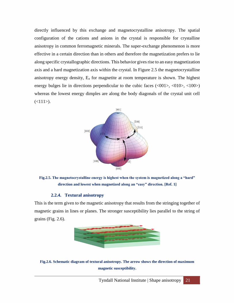
axis and a hard magnetization axis within the crystal. In Figure 2.5 the magnetocrystalline
anisotropy energy density, Ea for magnetite at room temperature is shown. The highest
energy bulges lie in directions perpendicular to the cubic faces (<001>, <010>, <100>)
whereas the lowest energy dimples are along the body diagonals of the crystal unit cell
(<111>).
Fig.2.5. The magnetocrystalline energy is highest when the system is magnetized along a “hard”
direction and lowest when magnetized along an “easy” direction. [Ref. 1]
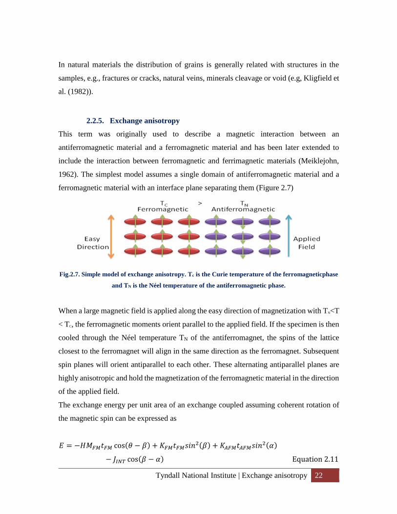
2.2.4. Textural anisotropy
This is the term given to the magnetic anisotropy that results from the stringing together of
magnetic grains in lines or planes. The stronger susceptibility lies parallel to the string of
grains (Fig. 2.6).
Fig.2.6. Schematic diagram of textural anisotropy. The arrow shows the direction of maximum
magnetic susceptibility.
Tyndall National Institute | Exchange anisotropy 22
In natural materials the distribution of grains is generally related with structures in the
samples, e.g., fractures or cracks, natural veins, minerals cleavage or void (e.g, Kligfield et
al. (1982)).
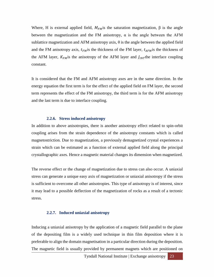
2.2.5. Exchange anisotropy
This term was originally used to describe a magnetic interaction between an
antiferromagnetic material and a ferromagnetic material and has been later extended to
include the interaction between ferromagnetic and ferrimagnetic materials (Meiklejohn,
1962). The simplest model assumes a single domain of antiferromagnetic material and a
ferromagnetic material with an interface plane separating them (Figure 2.7)
Fig.2.7. Simple model of exchange anisotropy. Tc is the Curie temperature of the ferromagneticphase
and TN is the Néel temperature of the antiferromagnetic phase.
When a large magnetic field is applied along the easy direction of magnetization with TN<T
< TC, the ferromagnetic moments orient parallel to the applied field. If the specimen is then
cooled through the Néel temperature TN of the antiferromagnet, the spins of the lattice
closest to the ferromagnet will align in the same direction as the ferromagnet. Subsequent
spin planes will orient antiparallel to each other. These alternating antiparallel planes are
highly anisotropic and hold the magnetization of the ferromagnetic material in the direction
of the applied field.
The exchange energy per unit area of an exchange coupled assuming coherent rotation of
the magnetic spin can be expressed as
𝐸 = −𝐻𝑀𝐹𝑀𝑡𝐹𝑀 cos(𝜃 − 𝛽) + 𝐾𝐹𝑀𝑡𝐹𝑀𝑠𝑖𝑛2(𝛽) + 𝐾𝐴𝐹𝑀𝑡𝐴𝐹𝑀𝑠𝑖𝑛2(𝛼)
− 𝐽𝐼𝑁𝑇 cos(𝛽 − 𝛼) Equation 2.11
Tyndall National Institute | Exchange anisotropy 23
Where, H is external applied field, 𝑀𝐹𝑀is the saturation magnetization, β is the angle
between the magnetization and the FM anisotropy, α is the angle between the AFM
sublattice magnetization and AFM anisotropy axis, θ is the angle between the applied field
and the FM anisotropy axis, 𝑡𝐹𝑀is the thickness of the FM layer, 𝑡𝐴𝐹𝑀is the thickness of
the AFM layer, 𝐾𝐹𝑀is the anisotropy of the AFM layer and 𝐽𝐼𝑁𝑇the interface coupling
constant.
It is considered that the FM and AFM anisotropy axes are in the same direction. In the
energy equation the first term is for the effect of the applied field on FM layer, the second
term represents the effect of the FM anisotropy, the third term is for the AFM anisotropy
and the last term is due to interface coupling.
2.2.6. Stress induced anisotropy
In addition to above anisotropies, there is another anisotropy effect related to spin-orbit
coupling arises from the strain dependence of the anisotropy constants which is called
magnetostriction. Due to magnetization, a previously demagnetized crystal experiences a
strain which can be estimated as a function of external applied field along the principal
crystallographic axes. Hence a magnetic material changes its dimension when magnetized.
The reverse effect or the change of magnetization due to stress can also occur. A uniaxial
stress can generate a unique easy axis of magnetization or uniaxial anisotropy if the stress
is sufficient to overcome all other anisotropies. This type of anisotropy is of interest, since
it may lead to a possible deflection of the magnetization of rocks as a result of a tectonic
stress.
2.2.7. Induced uniaxial anisotropy
Inducing a uniaxial anisotropy by the application of a magnetic field parallel to the plane
of the depositing film is a widely used technique in thin film deposition where it is
preferable to align the domain magnetisation in a particular direction during the deposition.
The magnetic field is usually provided by permanent magnets which are positioned on
Tyndall National Institute | Anisotropy control 24
either side of the substrate in which direction the uniaxial anisotropy needs to be created.
It is important that the field applied by the permanent magnets needs to be parallel to the
substrate surface and to minimise the number of flux lines which intersect the surface of
the substrate.
There are other ways to create uniaxial anisotropy. One of the most commonly used method
is thermal annealing. Macrosocpic anisotropy can be induced by applying a saturating
magnetic field during thermal treatment so that the domain structure of the magnetic
material consists of a single domain during the process. In voltage-driven spintronic
devices the induced anisotropy can be created by applying very high voltage during the
film deposition.
2.3. Anisotropy control
2.3.1. Crystal structure
Magnetocrystalline anisotropy is one of the fundamental parameters in the analysis of
magnetic behavior of magnetic materials. It can be easily observed by measuring
magnetization curves along different crystalline directions. Magnetocrystalline anisotropy
is the energy necessary to rotate the magnetic moment in a single crystal between the easy
and the hard directions. In single-domain particles or particles with low saturation
magnetizations the crystal structure of the materials dominates the magnetic energy. The
so-called easy directions of magnetization are crystallographic directions along which
magnetocrystalline energy is at a minimum. The magnetically easy and hard directions
arise due to the interaction of the spin magnetic moment within the crystal lattice known
as spin-orbit coupling. As a consequence of the magnetocrystalline anisotropy energy when
the magnetization is aligned in an easy direction, work must be performed to change the
magnetization in other direction. In order to switch from easy to hard direction or vice versa
the magnetization has to traverse a path over an energy barrier which is the difference
between the energy required for the spin to be aligned in the magnetically easy and hard
directions. In cubic crystals the magnetocrystalline anisotropy energy is given by an
exponential series in terms of the angles between the magnetization direction and the axes
Tyndall National Institute | Crystal structure 25
of crystal cube. The anisotropy energy can be represented in an arbitrary direction only by
the first two empirical constant terms in the series called the first- and second order
anisotropy constants, or 1k and 2k respectively.
The magnetic anisotropy in transition metals arises from spin-orbit coupling. The typical
fourth-order approximation of the parameterization of uniaxial anisotropy expressed in
terms of energy density is:
4
1
2
1
4
2
2
1 )(cos)(cos zzii
i
uni SkSkkkε Equation 2.12
Where,
i
uniε =The uniaxial anisotropy energy of a magnetic moment i
1k =The primary anisotropy constant of a material obtained from experimental
measurements, expressed as a temperature-dependent energy density
2k =The secondary anisotropy constant of a material obtained from experimental
measurements,
i = The angle between iS and the easy.
Both the constants ( 1k & 2k ) are expressed as a temperature-dependent energy density and
can exist with either a positive or negative sign. When 1k >1 the axis is easy, when 1k <0 the
axis becomes hard (which yields an easy plane).
By neglecting constant terms, an equivalent parameterisation can be written as:
)(sin)(sin 4
2
2
1 ii
i
uni kkε Equation 2.13
The typical cubic anisotropyparameterization is not straight forward trigonometrically:
)()( 222
2
2222
1 zyxzyyx
i
cub SSSkSSSSkε Equation 2.14
wherei
cubε is the cubic anisotropy energy of a magnetic moment ki .
Tyndall National Institute | Nanomodulation 26
The positive 1k yields easy axes along the body edges (100) and negative 1k indicates the
easy axes across the diagonals (111). [2]
The energy for a system of magnetic moments is given by:
i
i
cubah εε Equation 2.15
where, ahε is either uniε or cubε .
Materials like permalloys are considered isotropic (i.e. 1k = 2k = 0). The contribution to the
total energy from the anisotropy for such kind of materials is zero. To induce anisotropy in
those materials a novel technique such as nanomodulation technique is used, which is
discussed in the next section.
2.3.2. Nanomodulation
In recent years magnetic anisotropy has been demonstrated for patterned, isolated magnetic
structures [3-5] and structured continuous magnetic films [6]. Such kinds of control open
up opportunities for potential applications such as spintronic devices, magnetic random
access memory (MRAM) [7] high density patterned information storage media [7,8], and
high precision ultra-small magnetic field sensors [9]. Due to fundamental reasons and
potential applications, it is necessary to understand further the magnetic properties of
patterned structures in reduced dimensions, while both geometry and crystal microstructure
are needed to be optimized prior to configure the magnetization [10]. Subsequent
investigations further reveal fascinating properties like geometrical frustration, domain
wall pining, etc. due to dipolar interaction based on spin configurations [11,12]. Several
methods such as ion irradiation through a mask [6], selective epitaxy [13], surface
modulation [13], etc. have been studied to control the magnetization configuration in
patterned structures. In recent years Ion beam lithography has been found to be very useful
for transferring nanopatterns on three-dimensional surfaces. Ion beam lithography offers
more precise nanopattern than UV, X-ray, or electron beam lithography because in this
technique heavier particles with more momentum is used. Among all these, surface
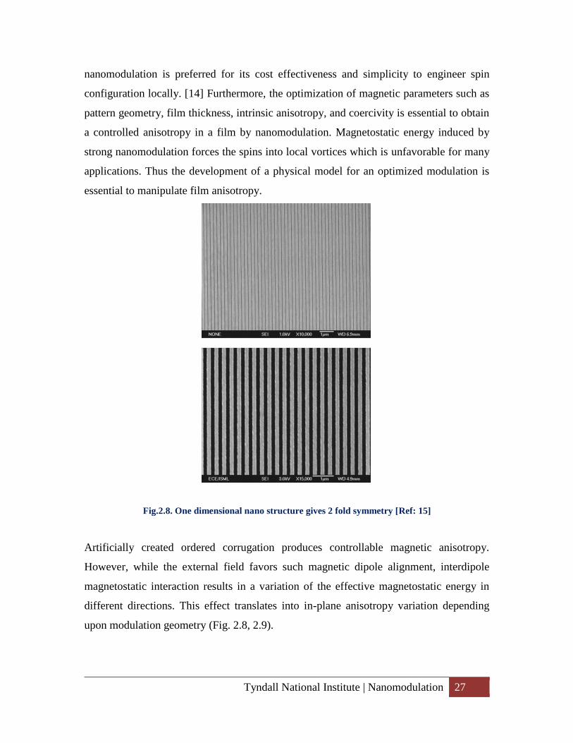
Tyndall National Institute | Nanomodulation 27
nanomodulation is preferred for its cost effectiveness and simplicity to engineer spin
configuration locally. [14] Furthermore, the optimization of magnetic parameters such as
pattern geometry, film thickness, intrinsic anisotropy, and coercivity is essential to obtain
a controlled anisotropy in a film by nanomodulation. Magnetostatic energy induced by
strong nanomodulation forces the spins into local vortices which is unfavorable for many
applications. Thus the development of a physical model for an optimized modulation is
essential to manipulate film anisotropy.
Fig.2.8. One dimensional nano structure gives 2 fold symmetry [Ref: 15]
Artificially created ordered corrugation produces controllable magnetic anisotropy.
However, while the external field favors such magnetic dipole alignment, interdipole
magnetostatic interaction results in a variation of the effective magnetostatic energy in
different directions. This effect translates into in-plane anisotropy variation depending
upon modulation geometry (Fig. 2.8, 2.9).
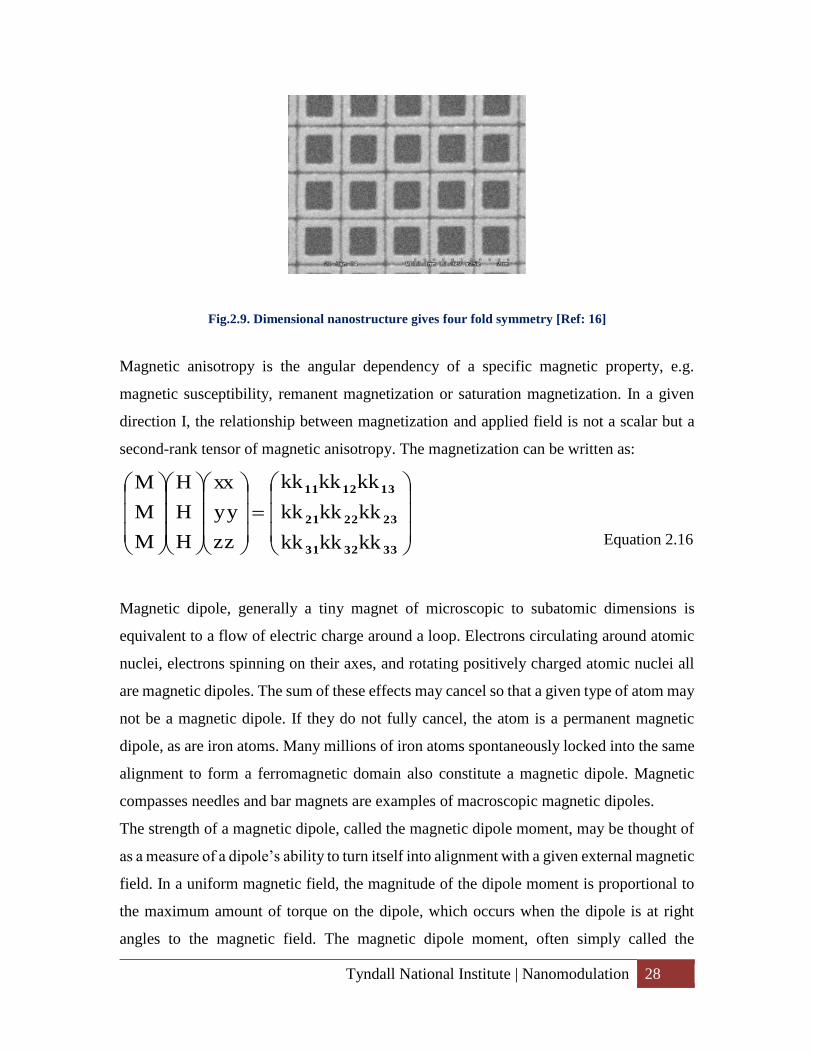
Tyndall National Institute | Nanomodulation 28
Fig.2.9. Dimensional nanostructure gives four fold symmetry [Ref: 16]
Magnetic anisotropy is the angular dependency of a specific magnetic property, e.g.
magnetic susceptibility, remanent magnetization or saturation magnetization. In a given
direction I, the relationship between magnetization and applied field is not a scalar but a
second-rank tensor of magnetic anisotropy. The magnetization can be written as:
333231
232221
131211
kkkkkk
kkkkkk
kkkkkk
zz
yy
xx
H
H
H
M
M
M
Equation 2.16
Magnetic dipole, generally a tiny magnet of microscopic to subatomic dimensions is
equivalent to a flow of electric charge around a loop. Electrons circulating around atomic
nuclei, electrons spinning on their axes, and rotating positively charged atomic nuclei all
are magnetic dipoles. The sum of these effects may cancel so that a given type of atom may
not be a magnetic dipole. If they do not fully cancel, the atom is a permanent magnetic
dipole, as are iron atoms. Many millions of iron atoms spontaneously locked into the same
alignment to form a ferromagnetic domain also constitute a magnetic dipole. Magnetic
compasses needles and bar magnets are examples of macroscopic magnetic dipoles.
The strength of a magnetic dipole, called the magnetic dipole moment, may be thought of
as a measure of a dipole’s ability to turn itself into alignment with a given external magnetic
field. In a uniform magnetic field, the magnitude of the dipole moment is proportional to
the maximum amount of torque on the dipole, which occurs when the dipole is at right
angles to the magnetic field. The magnetic dipole moment, often simply called the
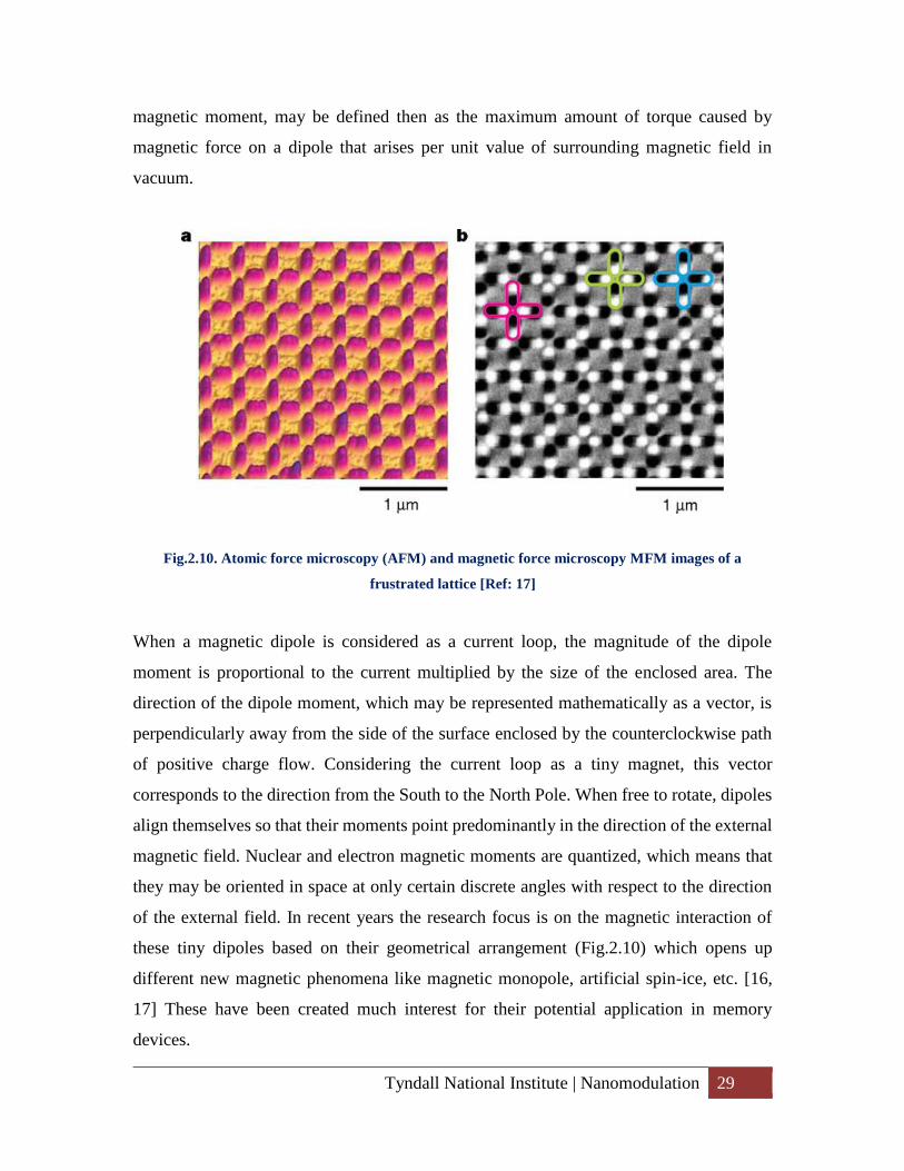
Tyndall National Institute | Nanomodulation 29
magnetic moment, may be defined then as the maximum amount of torque caused by
magnetic force on a dipole that arises per unit value of surrounding magnetic field in
vacuum.
Fig.2.10. Atomic force microscopy (AFM) and magnetic force microscopy MFM images of a
frustrated lattice [Ref: 17]
When a magnetic dipole is considered as a current loop, the magnitude of the dipole
moment is proportional to the current multiplied by the size of the enclosed area. The
direction of the dipole moment, which may be represented mathematically as a vector, is
perpendicularly away from the side of the surface enclosed by the counterclockwise path
of positive charge flow. Considering the current loop as a tiny magnet, this vector
corresponds to the direction from the South to the North Pole. When free to rotate, dipoles
align themselves so that their moments point predominantly in the direction of the external
magnetic field. Nuclear and electron magnetic moments are quantized, which means that
they may be oriented in space at only certain discrete angles with respect to the direction
of the external field. In recent years the research focus is on the magnetic interaction of
these tiny dipoles based on their geometrical arrangement (Fig.2.10) which opens up
different new magnetic phenomena like magnetic monopole, artificial spin-ice, etc. [16,
17] These have been created much interest for their potential application in memory
devices.
Tyndall National Institute | Exchange bias 30
For such application it is essential to control the dipolar or magnetostatic interaction at a
large scale. Magnetic dipole moments have dimensions of ‘current times area’ or ‘energy
divided by magnetic flux density’. In the MKS and SI systems, the specific unit for dipole
moment is A2m. In the CGS electromagnetic system, the unit is the erg (unit of energy) per
gauss (unit of magnetic flux density). One thousand ergs per gauss equal one ampere-
square metre. A convenient unit for the magnetic dipole moment of electrons is the Bohr
magneton (equivalent to 9.27 × 10⁻²⁴ A2m). A similar unit for magnetic moments of nuclei,
protons, and neutrons is the nuclear magneton (equivalent to 5.051 × 10⁻²⁷A2m).
2.3.3. Exchange bias
The shift of hysterecis loop, initially called exchange anisotropy was first reported by
Meiklejohn and Bean [18] in ferromagnetic (FM) Co particle encapsulated with
antiferromagnetic (FM) CoO as quoted by them “A new type of magnetic anisotropy has
been discovered which is best described as an exchange anisotropy. This anisotropy is the
result of an interaction between an antiferromagnetic material and a ferromagnetic
material”. Later the name exchange anisotropy was changed to exchange bias. In the more
than 60 years since its discovery, the phenomenon of exchange bias has become the basis
for different important applications in micromagnetic technology with surge in research
and development wordwide. However, it has only been within the last two decade or so
when the basic, quantitatively predictive, fundamental understanding of exchange bias has
been investigated significantly beyond the initial model presented by Meiklejohn and Bean.
Primarily, exchange bias is the result of exchange interactions between ferromagnetic (FM)
and anti-ferromagnetic (AFM) materials at the interface. Only recently these phenomena
have been investigated thoroughly due to the required experimental and analytical tools for
dealing with interfacial behavior at the atomic scale became available. Meiklejohn and
Bean's discovery was initiated by the observation of the hysteresis loop measured below
room temperature of a sample of nominal Co nanoparticles which was shifted along the
field axis after cooling in an external applied field. They described how the exchange
interaction across the interface between the FM Co and the AFM CoO could produce the
shift in hysteresis loop along field direction and manifests exchange bias (Fig. 2.11).
Tyndall National Institute | Exchange bias 31
Normally thr loop shift is measured after cooling under external magnetic field. The loop
shift is equivalent to the assumption of a unidirectional anisotropy energy for the free
energy at T=0 K of a single-domain spherical magnetic particle with uniaxial anisotropy.
The uniaxial anisotropy is aligned with its easy axis in the direction of the external magnetic
field(H) which is applied in the anti-parallel direction of particle's magnetization (Ms), i.e.,
𝐹 = 𝐻𝑀𝑆𝑐𝑜𝑠𝛩 − 𝐾𝑢𝑐𝑜𝑠𝛩 + 𝐾⟘ 𝑠𝑖𝑛2 𝛩 Equation 2.17
where Θ is the angle between the direction of magnetization and the easy direction of
magnetization, 𝐾𝑢 and 𝐾1are the unidirectional and uniaxial anisotropy energy constants
respectively.
Solutions of this equation can be expressed in terms of an effective field
𝐻′ = 𝐻 − 𝐾𝑢/𝑀𝑆 Equation 2.18
which gives the hysteresis loop displaced by 𝐾𝑢/𝑀𝑆 along the field axis. Thus, an
explanation of the loop shift is equivalent to explaining the interfacial unidirectional
anisotropy.
For more than a half century this phenomena has been studied due to its potential
applications in giant magneto resistance (GMR)[19], spin valve[20], high density storage
media[21] etc. as well as for fundamental studies. The conventional way to induce
exchange anisotropy, named exchange bias (EB) is to cool down a magnetically
uncompensated AFM-FM interface below Nee´l Temperature (TN) of AFM and Curie
Temperature (TC) of FM where TN<TC. A unidirectional shift of hysteresis or exchange
bias should be observed in exchange coupled FM-AFM interface. In most cases the
exchange bias is observed in the direction of cooling field, which is called positive EB.
Due to the AFM-FM interaction, the FM spins intend to point in the direction of the cooling
field at low temperatures below TN. In some cases due to the large unidirectional anisotropy
of AFM, the AFM-FM interfacial interaction biases FM spins to the opposite direction of
cooling field and causes a loop shift in opposite direction causing negative exchange bias.
In addition an enhancement of coercively is also observed [6-8, 22-24]. Conventional field
cooling is not necessary to introduce exchange bias in all cases. An exchange bias can be
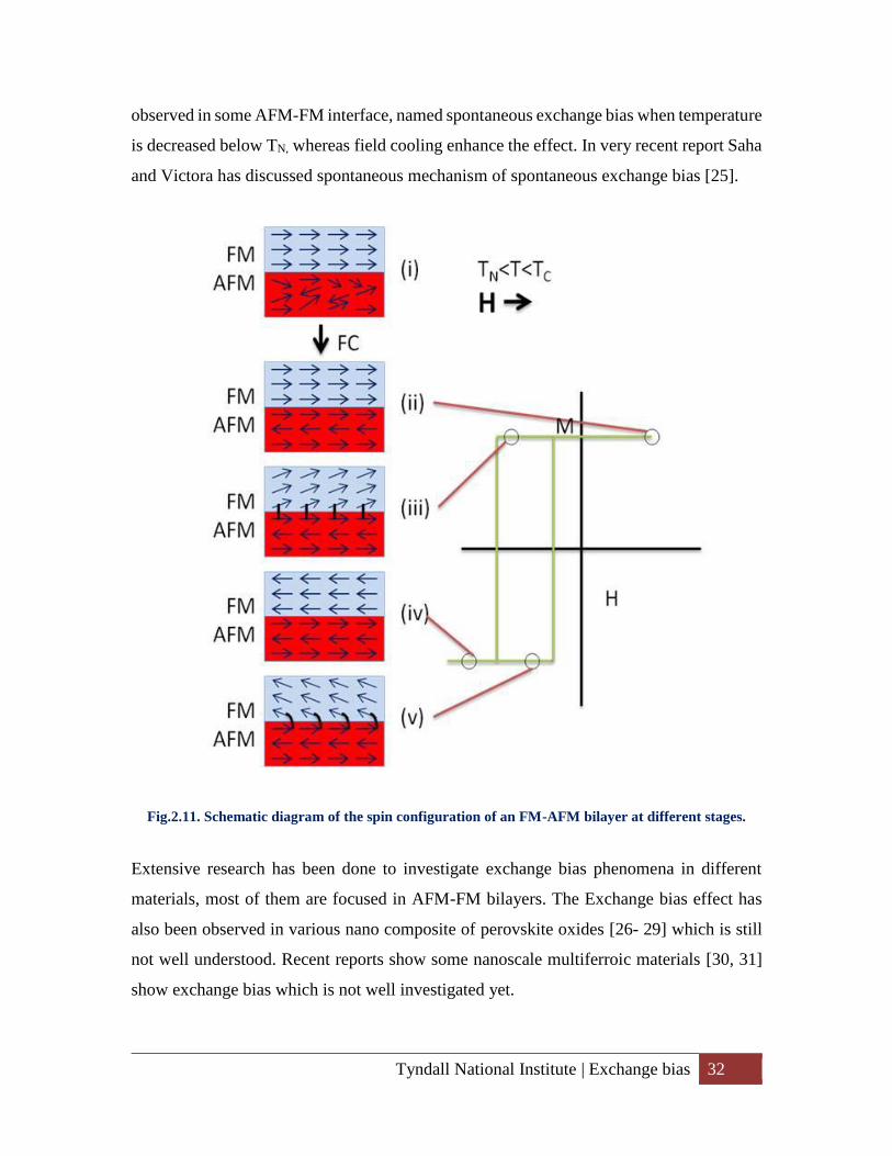
Tyndall National Institute | Exchange bias 32
observed in some AFM-FM interface, named spontaneous exchange bias when temperature
is decreased below TN, whereas field cooling enhance the effect. In very recent report Saha
and Victora has discussed spontaneous mechanism of spontaneous exchange bias [25].
Fig.2.11. Schematic diagram of the spin configuration of an FM-AFM bilayer at different stages.
Extensive research has been done to investigate exchange bias phenomena in different
materials, most of them are focused in AFM-FM bilayers. The Exchange bias effect has
also been observed in various nano composite of perovskite oxides [26- 29] which is still
not well understood. Recent reports show some nanoscale multiferroic materials [30, 31]
show exchange bias which is not well investigated yet.
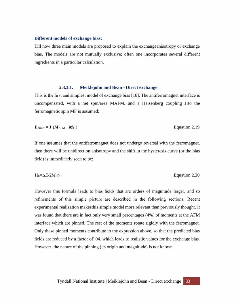
Tyndall National Institute | Meiklejohn and Bean - Direct exchange 33
Different models of exchange bias:
Till now three main models are proposed to explain the exchangeanisotropy or exchange
bias. The models are not mutually exclusive; often one incorporates several different
ingredients in a particular calculation.
2.3.3.1. Meiklejohn and Bean - Direct exchange
This is the first and simplest model of exchange bias [18]. The antiferromagnet interface is
uncompensated, with a net spin/area MAFM, and a Heisenberg coupling J1to the
ferromagnetic spin MF is assumed:
Edirect = J1(MAFM · MF ) Equation 2.19
If one assumes that the antiferromagnet does not undergo reversal with the ferromagnet,
then there will be unidirection anisotropy and the shift in the hysteresis curve (or the bias
field) is immediately seen to be:
HE=E/2MFtF Equation 2.20
However this formula leads to bias fields that are orders of magnitude larger, and so
refinements of this simple picture are described in the following sections. Recent
experimental realization makesthis simple model more relevant than previously thought. It
was found that there are in fact only very small percentages (4%) of moments at the AFM
interface which are pinned. The rest of the moments rotate rigidly with the ferromagnet.
Only these pinned moments contribute to the expression above, so that the predicted bias
fields are reduced by a factor of .04, which leads to realistic values for the exchange bias.
However, the nature of the pinning (its origin and magnitude) is not known.
Tyndall National Institute | Mauri - AFM spring: 34
2.3.3.2. Mauri - AFM spring:
Mauri realized that the exchange energy cost associated with reversal of the ferromagnet
can be decreased by accommodating a domain wall within the antiferromagnet. A form of
the energy function which accounts for this is given as follows:
𝐸 = −𝑯. 𝑴 −J1[𝑴. 𝒎] + /2. [1 − 𝒎. 𝒏] Equation 2.21
Here Mis the ferromagnetic orientation, m is the orientation of the net spin of the
antiferromagnet at the interface, u is the direction of the easy axis of the antiferromagnet;
it is assumed that far away from the interface the antiferromagnet has relaxed to point along
its easy axis. σ is the energy of a domain wall in the antiferromagnet. An expression for the
switching field can be found (here we assumed the external field points in the z-direction):
HE=J1(/2)uz/(J12+(/2)2-J1(M.u) Equation 2.22
If u is assumed to make an angle θ with the z-axis, then the above can be written:
𝐻𝐸 = (𝐽1/𝑀𝑡)cos 𝜃
(𝑟2+1+2𝑟|sin 𝜃|)1/2 Equation 2.23
with r =J/(σ/2). The important point to note is that the presence of the domain wall
decreases the bias field by a factor outside of the brackets - which for realistic parameters
can reduce the exchange bias field by one or two orders of magnitude, making the model
predictions consistent with experiments. Typically it is assumed that the domain wall is
present in the antiferromagnet (because of a weaker stiffness in the AFM). In the case where
r → ∞ (physically where the direct exchange J dominates, and is essentially frozen out of
the problem), the above expression indicates an energy cost associated with ferromagnet
reversal of σ - in this case, reversal costs the energy of 1 domain wall. If r → 0, the domain
wall (DW) is frozen out and we recover exchange bias HE=E/2MFtF.
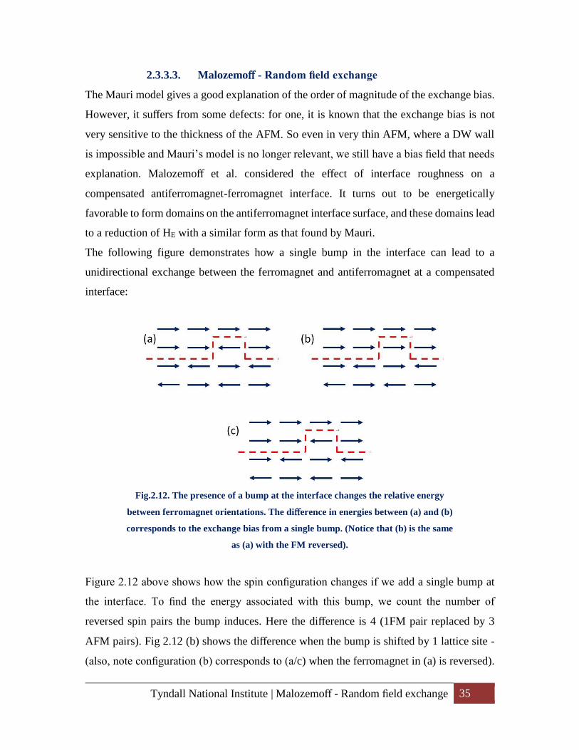
Tyndall National Institute | Malozemoff - Random field exchange 35
2.3.3.3. Malozemoff - Random field exchange
The Mauri model gives a good explanation of the order of magnitude of the exchange bias.
However, it suffers from some defects: for one, it is known that the exchange bias is not
very sensitive to the thickness of the AFM. So even in very thin AFM, where a DW wall
is impossible and Mauri’s model is no longer relevant, we still have a bias field that needs
explanation. Malozemoff et al. considered the effect of interface roughness on a
compensated antiferromagnet-ferromagnet interface. It turns out to be energetically
favorable to form domains on the antiferromagnet interface surface, and these domains lead
to a reduction of HE with a similar form as that found by Mauri.
The following figure demonstrates how a single bump in the interface can lead to a
unidirectional exchange between the ferromagnet and antiferromagnet at a compensated
interface:
Fig.2.12. The presence of a bump at the interface changes the relative energy
between ferromagnet orientations. The difference in energies between (a) and (b)
corresponds to the exchange bias from a single bump. (Notice that (b) is the same
as (a) with the FM reversed).
Figure 2.12 above shows how the spin configuration changes if we add a single bump at
the interface. To find the energy associated with this bump, we count the number of
reversed spin pairs the bump induces. Here the difference is 4 (1FM pair replaced by 3
AFM pairs). Fig 2.12 (b) shows the difference when the bump is shifted by 1 lattice site -
(also, note configuration (b) corresponds to (a/c) when the ferromagnet in (a) is reversed).
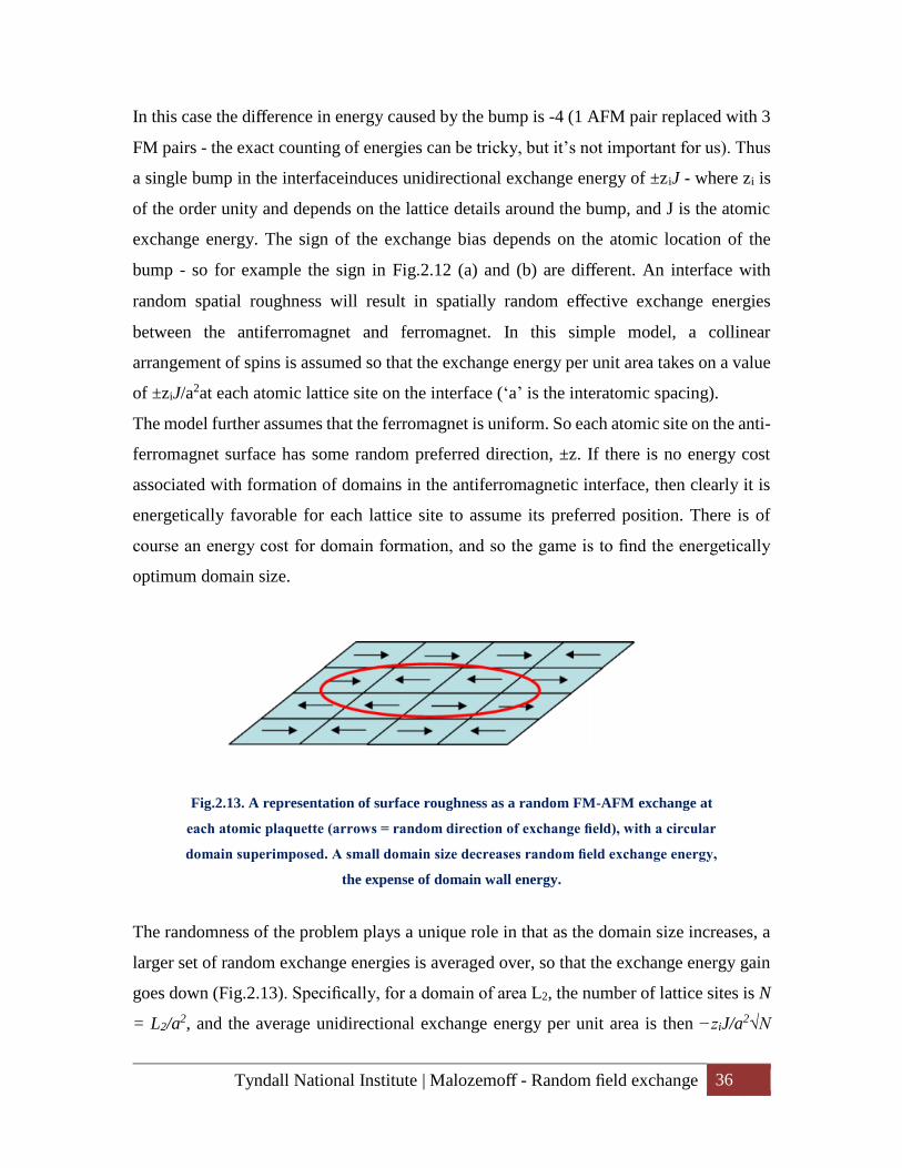
Tyndall National Institute | Malozemoff - Random field exchange 36
In this case the difference in energy caused by the bump is -4 (1 AFM pair replaced with 3
FM pairs - the exact counting of energies can be tricky, but it’s not important for us). Thus
a single bump in the interfaceinduces unidirectional exchange energy of ±ziJ - where zi is
of the order unity and depends on the lattice details around the bump, and J is the atomic
exchange energy. The sign of the exchange bias depends on the atomic location of the
bump - so for example the sign in Fig.2.12 (a) and (b) are different. An interface with
random spatial roughness will result in spatially random effective exchange energies
between the antiferromagnet and ferromagnet. In this simple model, a collinear
arrangement of spins is assumed so that the exchange energy per unit area takes on a value
of ±ziJ/a2at each atomic lattice site on the interface (‘a’ is the interatomic spacing).
The model further assumes that the ferromagnet is uniform. So each atomic site on the anti-
ferromagnet surface has some random preferred direction, ±z. If there is no energy cost
associated with formation of domains in the antiferromagnetic interface, then clearly it is
energetically favorable for each lattice site to assume its preferred position. There is of
course an energy cost for domain formation, and so the game is to find the energetically
optimum domain size.
Fig.2.13. A representation of surface roughness as a random FM-AFM exchange at
each atomic plaquette (arrows = random direction of exchange field), with a circular
domain superimposed. A small domain size decreases random field exchange energy,
the expense of domain wall energy.
The randomness of the problem plays a unique role in that as the domain size increases, a
larger set of random exchange energies is averaged over, so that the exchange energy gain
goes down (Fig.2.13). Specifically, for a domain of area L2, the number of lattice sites is N
= L2/a2, and the average unidirectional exchange energy per unit area is then −ziJ/a2√N
Tyndall National Institute | Koon/Butler - Spin-flop coupling 37
=−zi/aL. Mazeloff does the calculation to find the optimum domain size L, finding: L
≃π(A/K)1/2. This leads to a unidirectional exchange energy of zi (KA)1/2, or a bias field of
HE=(KA)1/2/2MFtF Equation 2.24
which is the same form found in Meiklejohn and Bean model (in the r → ∞ limit). This
model can explain the order of magnitude of HE for very thin AFM layers. The notion of
DW formation on the surface of the AFM as the source of exchange bias is a feature of
more modern and elaborate theories of exchange bias.
2.3.3.4. Koon/Butler - Spin-flop coupling
Koon found that at a perfectly compensated interface, the interface spins of the
antiferromagnet will cant slightly out of the plane. A perfectly compensated interface will
decrease its energy by canting slightly out of the plane, towards the FM. This results in a
small net moment which couples to the FM, and leads to a spin-flop coupling between the
FM and the axis of the AFM.There will be a small net moment which is perpindicular to
the axis of the antiferromagnet. This moment will couple to the ferromagnet, and leads to
spin-flop coupling like interaction K2(MF · MAFM)2. Adding this term to the energy,one
obtains:
E = −H· M − J[M· m] + Jsf[M· m]2+(σ/2)[1 − m · u] Equation 2.25
Koon initially proposed that this coupling can lead to unidirectional anisotropy, or
exchange bias. The mechanism is Mauri-like, in that it relies on partial longitudinal domain
wall formation in the antiferromagnet. This result was initially supported by atomistic
calculations of Koon (done with an XY-model, or strictly easy plane limitation). However,
Butler et al. reportedmore detailed calculations which allow for out-of-plane spins, and
including magnetostatic interactions. They found that a pure spin-flop coupling for
Heisenberg spin term does not give rise to exchange bias. The extra freedom allowed in
Butler’s calculation allowed the antiferromagnetic orientation to switch between its
degenerate minima before a domain wall is formed. This spin-flop coupling can, however,
account for the enhanced hysteresis of the ferromagnet, Butler used a combination of spin-
flop coupling, and Malozemoff random field effects to find realistic values for the exchange
Tyndall National Institute | Different magnetic phenomena out of
nanostrcutures
38
bias. Stiles et al found that the addition of spin-flop coupling actually reduces the exchange
bias field in the simple model given by above equation.
2.4 Different magnetic phenomena out of nanostrcutures
2.4.1. Superparamagnetism Superparamagnetism (SPM) is a type of magnetism which occurs in small ferrimagnetic or
ferromagnetic nanoparticles with size around a few nanometers to a couple of tenth of
nanometers, depending on the materials. In a simple approximation, when the size of the
nanoparticle are smaller than its single domain size the total magnetic moment of the
nanoparticle can be regarded as one giant magnetic moment, composed of all the individual
magnetic moments of the atoms of nanoparticle. These nanoparticles are called
superparamagnetic nanoparticles. In such nanoparticles having5 uniaxial anisotropy,
magnetization can randomly flip direction under the influence of temperature. The typical
time between two flips is called the Néel relaxation time:
𝜏 = 𝜏0𝑒𝑥𝑝 (𝛥𝐸
𝑘𝐵𝑇)
Where,
𝜏0=The length of time characteristic of the probed material.
∆he length of barrier the magnetization flip has to overcome by thermal energy.
kB: The Boltzmann constant
T: Temperature.
The observation of superparamagnetic state in nanoparticles does only depend on the
temperature T and energy barrier ΔE but also measurement time τm of each experimental
technique. Depending on the measuremnt time two scenarios can occur. When the
measurement time is much smaller than the relaxation time, a well defined blocked state
can be observed. If the measurement tttime is much larger than the relaxation time a time-
averaged net zero magnetic moment is observed due to the fluctuation state of
magnetization which is called superparamagnetism.
Tyndall National Institute | Superferromagnetism 39
2.4.2. Superferromagnetism Superferromagnetism is the magnetic state of an ensemble of magnetically interacting very
small size (nano) magnetic material with super-moment. In the case of diluted nanoparticle
systems where the magnetic interactions between particles are ignored, it is a
superparamagnetic state of the nanoparticles due to the absence of a collective order. For
highly dense nanoparticles with strong magnetic interactions, it can reach a
superferromagnetism stage due to a collective ferromagnetic order. For example,
nanoparticles of ferrihydrite (nominally FeOOH) like iron oxides interact magnetically and
due to the interactions the magnetic behaviours of the nanoparticles (both above and below
their blocking temperatures TB) are changed and lead to an ordered low-temperature phase
with non-randomly oriented particle with super-moments which is called
superferromagnetism.
2.4.3. Super Spin Glass A spin glass is a disordered magnet, where the magnetic spin of the component atoms (the
orientation of the north and south magnetic poles in three-dimensional space) are not
aligned in a regular pattern. The spin glass is a random mixed-interactingsystem
characterized by randomness and freezing of spins at a well-defined temperature Tf. Below
the temperature a highly irreversible metastable frozen state generates without the usual
long-range spatial magnetic order. The two most important charecteristics of spin glasses
are, randomness in either position of the spins or the sign of interactions with neighbouring
spin. Also a disordered, site or bond is required to create a spin glass. Otherwise the
magnetic transition will be considered as standard ferromagnetic or antiferromagnetic type
of long-range order. The term "glass" comes from an analogy from the positional disorder
of a conventional, chemical glass, e.g., a window glass to the magnetic disorder in a spin
glass. In amorphous solids like window glass, the atomic bond structures are highly
disordered or irregular whereas in a crystal has a uniform pattern of atomic bonds.
In magnetic nanoparticle systems, the particale size are smaller than single magnetic
domain size and become superparamagnetic which interacts to each other weakly.
Magnetic moments of each nanoparticle are called superspins, and such weakly interacting
magnetic nanoparticle systems are called superparamagnets. For dense magnetic
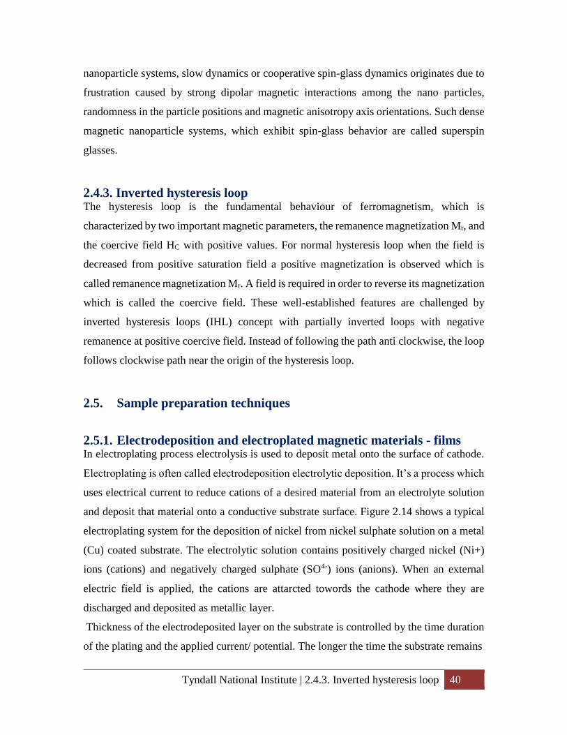
Tyndall National Institute | 2.4.3. Inverted hysteresis loop 40
nanoparticle systems, slow dynamics or cooperative spin-glass dynamics originates due to
frustration caused by strong dipolar magnetic interactions among the nano particles,
randomness in the particle positions and magnetic anisotropy axis orientations. Such dense
magnetic nanoparticle systems, which exhibit spin-glass behavior are called superspin
glasses.
2.4.3. Inverted hysteresis loop The hysteresis loop is the fundamental behaviour of ferromagnetism, which is
characterized by two important magnetic parameters, the remanence magnetization Mr, and
the coercive field HC with positive values. For normal hysteresis loop when the field is
decreased from positive saturation field a positive magnetization is observed which is
called remanence magnetization Mr. A field is required in order to reverse its magnetization
which is called the coercive field. These well-established features are challenged by
inverted hysteresis loops (IHL) concept with partially inverted loops with negative
remanence at positive coercive field. Instead of following the path anti clockwise, the loop
follows clockwise path near the origin of the hysteresis loop.
2.5. Sample preparation techniques
2.5.1. Electrodeposition and electroplated magnetic materials - films In electroplating process electrolysis is used to deposit metal onto the surface of cathode.
Electroplating is often called electrodeposition electrolytic deposition. It’s a process which
uses electrical current to reduce cations of a desired material from an electrolyte solution
and deposit that material onto a conductive substrate surface. Figure 2.14 shows a typical
electroplating system for the deposition of nickel from nickel sulphate solution on a metal
(Cu) coated substrate. The electrolytic solution contains positively charged nickel (Ni+)
ions (cations) and negatively charged sulphate (SO4-) ions (anions). When an external
electric field is applied, the cations are attarcted towords the cathode where they are
discharged and deposited as metallic layer.
Thickness of the electrodeposited layer on the substrate is controlled by the time duration
of the plating and the applied current/ potential. The longer the time the substrate remains
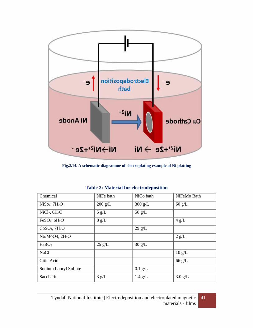
Tyndall National Institute | Electrodeposition and electroplated magnetic
materials - films
41
Fig.2.14. A schematic diagramme of electroplating example of Ni platting
Table 2: Material for electrodeposition
Chemical NiFe bath NiCo bath NiFeMo Bath
NiSo4, 7H2O 200 g/L 300 g/L 60 g/L
NiCl2, 6H2O 5 g/L 50 g/L
FeSO4, 6H2O 8 g/L 4 g/L
CoSO4, 7H2O 29 g/L
Na2MoO4, 2H2O 2 g/L
H3BO3 25 g/L 30 g/L
NaCl 10 g/L
Citic Acid 66 g/L
Sodium Lauryl Sulfate 0.1 g/L
Saccharin 3 g/L 1.4 g/L 3.0 g/L
Tyndall National Institute | Sonochemical methods - nanocomposites 42
in the operating plating bath, the thicker the resulting electroplated layer will be. The
thickness depends on applied current/ potential across the two electrodes as well. Typically
thicknesses of the film can be varied from 100 nm to 30 microns. An electroplated layer is
genrally composed of a single metallic material. Co-deposition of two or more metals such
as a Cu-Zn alloy, Au-Sn alloy or Ni-Fe alloy is possible under suitable bath conditions.
The development of micromagneic devices has widely based on the use of electroplated
nickel-iron permalloy since it has good soft magnetic properties, high permeability, stable
high frequency responses, etc. [28-30] Initially electroplated permalloy (Ni/Fe 80/20) has
been widely used for micromagnetic devices. Later other alloy materials like NiFeMo, Ni-
17Fe-4Mo, etc. have been investigated and used for better magnetic and mechanical
properties [31-32]. Depending on the material composition the baths are prepared. Samples
are electroplated on Si/Glass substrates with conducting titanium/gold/copper seed layer.
Depending on alloy composition and deposition current, voltage, bath temperature,
magnetic stirrer speed, external magnetic field, etc. are applied.
2.5.2. Sonochemical methods - nanocomposites Researchers have recently developed sonochemical methods for the preparation of
nanoparticles with controllable morphologies [33-34]. Ultrasound has become an
important tool for the synthesis of different nanoparticles. Ultrasonic cavitation is formed
when liquids are irradiated with ultrasonic irradiation. Ultrasonic cavitation which is is
concerned with the formation, growth, and implosive collapse of bubbles, produces a
variety of physical and chemical effects, such as high pressure (>20 MPa), temperature
(>5000 K) and cooling rate (>1010 K s-1), which could provide a unique environment for
chemical reactions under extreme conditions to prepare nanoparticles. Different research
groups have demonstrated that ultrasound is a fine method to preparae nanoparticles with
different controllable morphologies, such as dendritic, flowery, star-like, etc. It has been
demonstrated that the ultrasonic irradiation plays a crucial role in the morphology of the
product.
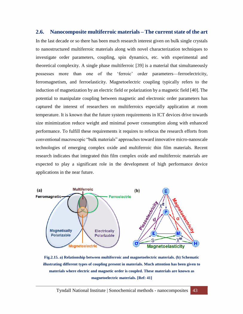
Tyndall National Institute | Sonochemical methods - nanocomposites 43
2.6. Nanocomposite multiferroic materials – The current state of the art
In the last decade or so there has been much research interest given on bulk single crystals
to nanostructured multiferroic materials along with novel characterization techniques to
investigate order parameters, coupling, spin dynamics, etc. with experimental and
theoretical complexity. A single phase multiferroic [39] is a material that simultaneously
possesses more than one of the ‘ferroic’ order parameters—ferroelectricity,
ferromagnetism, and ferroelasticity. Magnetoelectric coupling typically refers to the
induction of magnetization by an electric field or polarization by a magnetic field [40]. The
potential to manipulate coupling between magnetic and electronic order parameters has
captured the interest of researchers on multiferroics especially application at room
temperature. It is known that the future system requirements in ICT devices drive towards
size minimization reduce weight and minimal power consumption along with enhanced
performance. To fulfill these requirements it requires to refocus the research efforts from
conventional macroscopic “bulk materials” approaches toward innovative micro-nanoscale
technologies of emerging complex oxide and multiferroic thin film materials. Recent
research indicates that integrated thin film complex oxide and multiferroic materials are
expected to play a significant role in the development of high performance device
applications in the near future.
Fig.2.15. a) Relationship between multiferroic and magnetoelectric materials. (b) Schematic
illustrating different types of coupling present in materials. Much attention has been given to
materials where electric and magnetic order is coupled. These materials are known as
magnetoelectric materials. [Ref: 41]
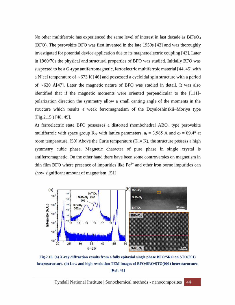
Tyndall National Institute | Sonochemical methods - nanocomposites 44
No other multiferroic has experienced the same level of interest in last decade as BiFeO3
(BFO). The perovskite BFO was first invented in the late 1950s [42] and was thoroughly
investigated for potential device application due to its magnetoelectric coupling [43]. Later
in 1960/70s the physical and structural properties of BFO was studied. Initially BFO was
suspected to be a G-type antiferromagnetic, ferroelectric multiferroic material [44, 45] with
a N´eel temperature of ∼673 K [46] and possessed a cycloidal spin structure with a period
of ∼620 Å[47]. Later the magnetic nature of BFO was studied in detail. It was also
identified that if the magnetic moments were oriented perpendicular to the [111]-
polarization direction the symmetry allow a small canting angle of the moments in the
structure which results a weak ferromagnetism of the Dzyaloshinskii–Moriya type
(Fig.2.15.) [48, 49].
At ferroelectric state BFO possesses a distorted rhombohedral ABO3 type perovskite
multiferroic with space group R3c with lattice parameters, ar = 3.965 Å and αr = 89.4° at
room temperature. [50] Above the Curie temperature (TC= K), the structure possess a high
symmetry cubic phase. Magnetic character of pure phase in single crystal is
antiferromagnetic. On the other hand there have been some controversies on magnetism in
thin film BFO where presence of impurities like Fe2+ and other iron borne impurities can
show significant amount of magnetism. [51]
Fig.2.16. (a) X-ray diffraction results from a fully epitaxial single phase BFO/SRO on STO(001)
heterostructure. (b) Low and high resolution TEM images of BFO/SRO/STO(001) heterostructure.
[Ref: 41]
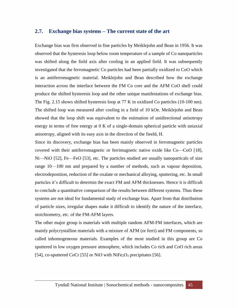
Tyndall National Institute | Sonochemical methods - nanocomposites 45
2.7. Exchange bias systems – The current state of the art
Exchange bias was first observed in fine particles by Meiklejohn and Bean in 1956. It was
observed that the hysteresis loop below room temperature of a sample of Co nanoparticles
was shifted along the field axis after cooling in an applied field. It was subsequently
investigated that the ferromagnetic Co particles had been partially oxidized to CoO which
is an antiferromagnetic material. Meiklejohn and Bean described how the exchange
interaction across the interface between the FM Co core and the AFM CoO shell could
produce the shifted hysteresis loop and the other unique manifestations of exchange bias.
The Fig. 2.15 shows shifted hysteresis loop at 77 K in oxidized Co particles (10-100 nm).
The shifted loop was measured after cooling in a field of 10 kOe. Meiklejohn and Bean
showed that the loop shift was equivalent to the estimation of unidirectional anisotropy
energy in terms of free energy at 0 K of a single-domain spherical particle with uniaxial
anisotropy, aligned with its easy axis in the direction of the fieeld, H.
Since its discovery, exchange bias has been mainly observed in ferromagnetic particles
covered with their antiferromagnetic or ferrimagnetic native oxide like Co—CoO [18],
Ni—NiO [52], Fe—FeO [53], etc. The particles studied are usually nanoparticals of size
range 10—100 nm and prepared by a number of methods, such as vapour deposition,
electrodeposition, reduction of the oxalate or mechanical alloying, sputtering, etc. In small
particles it’s difficult to determin the exact FM and AFM thicknesses. Hence it is difficult
to conclude a quantitative comparison of the results between different systems. Thus these
systems are not ideal for fundamental study of exchange bias. Apart from that distribution
of particle sizes, irregular shapes make it difficult to identify the nature of the interface,
stoichiometry, etc. of the FM-AFM layers.
The other major group is materials with multiple random AFM-FM interfaces, which are
mainly polycrystalline materials with a mixture of AFM (or ferri) and FM components, so
called inhomogeneous materials. Examples of the most studied in this group are Co
sputtered in low oxygen pressure atmosphere, which includes Co rich and CoO rich areas
[54], co-sputtered CoCr [55] or NiO with NiFe2O3 precipitates [56].
Tyndall National Institute | Sonochemical methods - nanocomposites 46
Fig.2.17. Exchange anisotropy first observed by W. Meiklejohn and C. P. Bean on Co-CoO particle
at 77K after field cooled [Ref: 18]
Exchange bias has been mostly studied in the materials in thin film form. In such systems
the interface can be effectively controlled and well characterized [57, 58]. From the
application point of view as well, most of the device applications are based on thin film
systems of exchange bias [59, 60]. Moreover, in thin film systems there are many basic
interesting parameters like AFM thickness [61], interface disorder [58], orientation
dependence of HE [57], multi FM-AFM layers, etc. which open up new functionality in the
exchange bias phenomenon. Among the layered systems, though AFM-FM interfaces
based exchange bias are the most investigated, however other related systems such as
AFM-ferri [62], ferri-ferri [63], ferri-FM [64] have also been investigated. The exchange
bias based on AFM-FM interface can be divided in three main categories depending on
AFM part: oxide, metallic and others. In this thesis both oxide and metallic materials have
been thoroughly investigated for exchange bias studies.
Tyndall National Institute | Chapter – Experimental techniques 47
3. Chapter – Experimental techniques
3.1. Magnetic Characterizations of Materials
3.1.1. Introduction to Magnetic characterization:
The materials were characterized in our magnetic characterization laboratory using two
different instruments, an SHB instruments (Mesa 200-HF) Magnetic Measurement System
real time B-H loop tracer and a Quantum Designs MPMS-XL5 superconducting quantum
interference device (SQUID). An overview of this process and some of the results to date
are outlined in this section. The first step prior to examining the results is to outline the
operation of the instruments used.
The first instrument is a B-H loop tracer (hence forth referred to simply as the SHB)
which was initially used to characterise thin-film samples. This instrument has the
advantage of being a real time measurement at room temperature, allowing samples to
be analysed quickly and inexpensively. All thin-film samples were analysed using this
instrument.
A selection of samples was chosen to be analysed using the Superconducting Quantum
Interference Device (henceforth referred to as the SQUID) which is a far more sensitive
instrument. A selection of thin-film and powder samples were measured, with room
temperature and low temperature (down to 10K) measurements being performed.
3.1.2. Characterization of materials with the hysteresis loop tracer
For this work hysteresis loop tracer (MESA 200 HF) by SHB Instruments Inc. [65] was
used which measures in the frequency range of 10 Hz and below. The mechanism of real
time hysteresis loop tracer is to apply an AC magnetic field to the sample (thin film) and
measure the flux density as a function of applied field generated by the magnetic coil where
the sample acts like core material for the coil. To obtain the magnetic induction the
response voltage from the sense coil is integrated by the instrument. In absence of a sample
the instrument would still show an elliptical loop from the sensor coil itself due to the
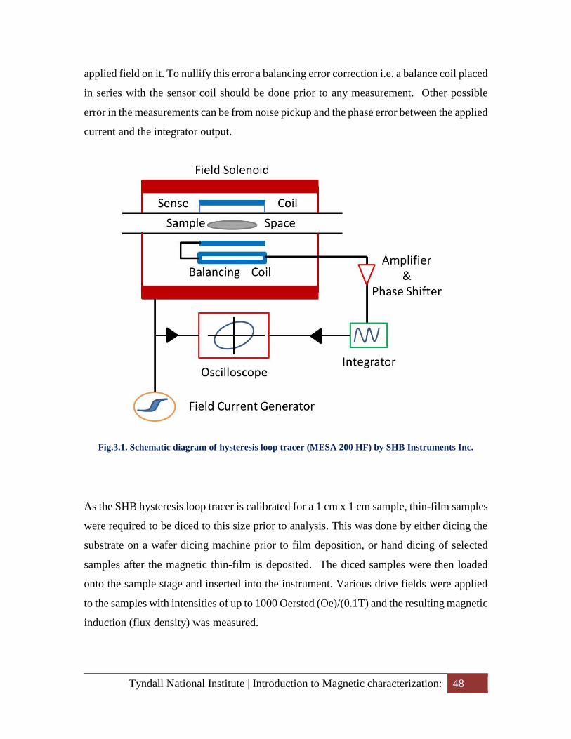
Tyndall National Institute | Introduction to Magnetic characterization: 48
applied field on it. To nullify this error a balancing error correction i.e. a balance coil placed
in series with the sensor coil should be done prior to any measurement. Other possible
error in the measurements can be from noise pickup and the phase error between the applied
current and the integrator output.
Fig.3.1. Schematic diagram of hysteresis loop tracer (MESA 200 HF) by SHB Instruments Inc.
As the SHB hysteresis loop tracer is calibrated for a 1 cm x 1 cm sample, thin-film samples
were required to be diced to this size prior to analysis. This was done by either dicing the
substrate on a wafer dicing machine prior to film deposition, or hand dicing of selected
samples after the magnetic thin-film is deposited. The diced samples were then loaded
onto the sample stage and inserted into the instrument. Various drive fields were applied
to the samples with intensities of up to 1000 Oersted (Oe)/(0.1T) and the resulting magnetic
induction (flux density) was measured.
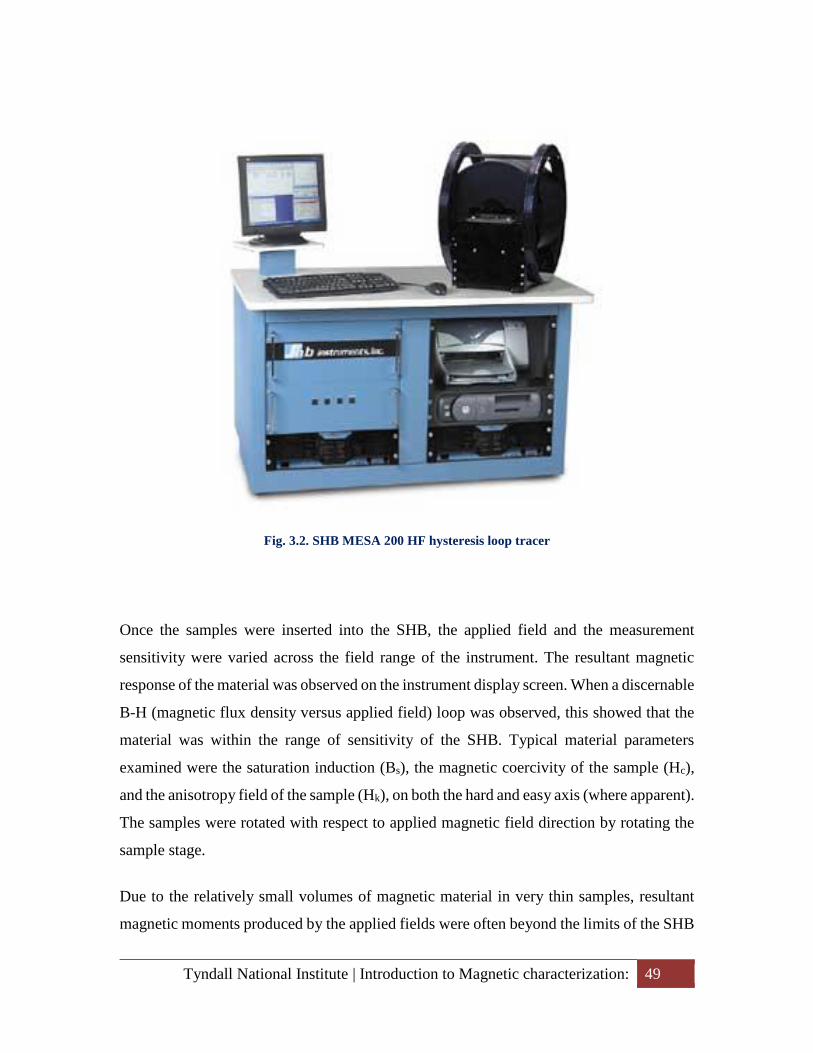
Tyndall National Institute | Introduction to Magnetic characterization: 49
Fig. 3.2. SHB MESA 200 HF hysteresis loop tracer
Once the samples were inserted into the SHB, the applied field and the measurement
sensitivity were varied across the field range of the instrument. The resultant magnetic
response of the material was observed on the instrument display screen. When a discernable
B-H (magnetic flux density versus applied field) loop was observed, this showed that the
material was within the range of sensitivity of the SHB. Typical material parameters
examined were the saturation induction (Bs), the magnetic coercivity of the sample (Hc),
and the anisotropy field of the sample (Hk), on both the hard and easy axis (where apparent).
The samples were rotated with respect to applied magnetic field direction by rotating the
sample stage.
Due to the relatively small volumes of magnetic material in very thin samples, resultant
magnetic moments produced by the applied fields were often beyond the limits of the SHB
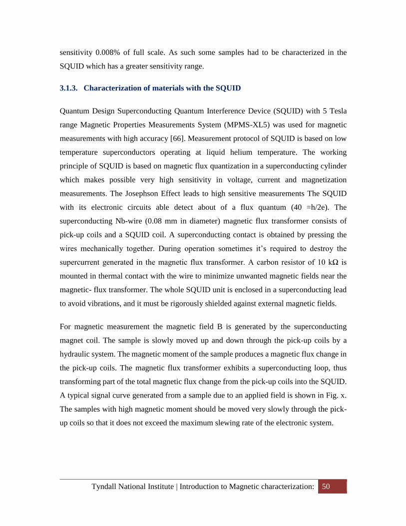
Tyndall National Institute | Introduction to Magnetic characterization: 50
sensitivity 0.008% of full scale. As such some samples had to be characterized in the
SQUID which has a greater sensitivity range.
3.1.3. Characterization of materials with the SQUID
Quantum Design Superconducting Quantum Interference Device (SQUID) with 5 Tesla
range Magnetic Properties Measurements System (MPMS-XL5) was used for magnetic
measurements with high accuracy [66]. Measurement protocol of SQUID is based on low
temperature superconductors operating at liquid helium temperature. The working
principle of SQUID is based on magnetic flux quantization in a superconducting cylinder
which makes possible very high sensitivity in voltage, current and magnetization
measurements. The Josephson Effect leads to high sensitive measurements The SQUID
with its electronic circuits able detect about of a flux quantum (40 =h/2e). The
superconducting Nb-wire (0.08 mm in diameter) magnetic flux transformer consists of
pick-up coils and a SQUID coil. A superconducting contact is obtained by pressing the
wires mechanically together. During operation sometimes it’s required to destroy the
supercurrent generated in the magnetic flux transformer. A carbon resistor of 10 kΩ is
mounted in thermal contact with the wire to minimize unwanted magnetic fields near the
magnetic- flux transformer. The whole SQUID unit is enclosed in a superconducting lead
to avoid vibrations, and it must be rigorously shielded against external magnetic fields.
For magnetic measurement the magnetic field B is generated by the superconducting
magnet coil. The sample is slowly moved up and down through the pick-up coils by a
hydraulic system. The magnetic moment of the sample produces a magnetic flux change in
the pick-up coils. The magnetic flux transformer exhibits a superconducting loop, thus
transforming part of the total magnetic flux change from the pick-up coils into the SQUID.
A typical signal curve generated from a sample due to an applied field is shown in Fig. x.
The samples with high magnetic moment should be moved very slowly through the pick-
up coils so that it does not exceed the maximum slewing rate of the electronic system.
Tyndall National Institute | Introduction to Magnetic characterization: 51
Fig.3.3. Output voltage vs. sample position plot, as a result of moving the sample through the pickup
coils under an applied field.
A Prior to running samples on the SQUID, the samples were prepared by dicing them into
a suitable size. The maximum size of a sample which can be inserted into the SQUID using
the standard transport is approximately 6mm x 15 mm. To minimize the impact of shape
anisotropy effect we diced the samples into a 4mm x 4mm size. They were then placed
into a sample holder and inserted into the SQUID. The SQUID is calibrated to take account
of the magnetic contribution of the straw, which may distort the measurements. The
samples are next centered by applying a magnetic field sufficiently high so as to saturate
the sample (up to 5T) and moving the sample through the SQUID’s measurement coils.
The operator then defines the center of the sample by visually inspecting the resultant
centering curves and aligning the maximum point of the curve to the corresponding center
point of the chamber. Once the sample is correctly loaded and centred, fields were applied
to the samples varying from + 50000 Oe to -50000 Oe and the resultant magnetizationof
the samples, in units of emu (electromagnetic units, 1000 emu/cm3= 1 A/m), was measured.

Tyndall National Institute | Introduction to Magnetic characterization: 52
Fig. 3.4. SQUID Magnetometer by Quantum Design
The SQUID measurement results are optimum in terms of time and accuracy for this unique
new category of material. Both DC (or static) measurements (where the moment is
measured in the prensence of a static magnetic field), as well as RSO (reciprocating sample
option, where the sample is moved up and down relative to the pick-up coils in the presence
of a static magnetic field) techniques were employed in the SQUID. For samples with low
magnetic moments (not strongly ferromagnetic) both DC and RSO multimeasure
techniques were used. This utilised a feature of the SQUID which measured the sample’s
magnetic moment many times and then applied statistical techniques to decide whether
subsequent measurements were required to ensure that a certain percentage of the resultant
magnetic moments fell within 2 sigma of the mean response. While the SQUID has a
theoretical sensitivity and measurement sensitivity of 10-8 emu, in practice this requires
both a prohibitively large amount of time and by extension liquid He to measure such
samples on the SQUID.
Magnetic measurements using SQUID magnetometer:
High sensitivity magnetometry to measure magnetic susceptibilities is carried out in a
SQUID (Superconducting Quantum Interference Devices) magnetometer. An equivalent
SQUID circuit [67] is shown in Fig.3.5. A closed superconducting loop, which consists of
a pickup coil and input coil, is shown in the figure. A persistent current is generated in the
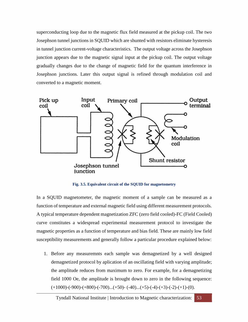
Tyndall National Institute | Introduction to Magnetic characterization: 53
superconducting loop due to the magnetic flux field measured at the pickup coil. The two
Josephson tunnel junctions in SQUID which are shunted with resistors eliminate hysteresis
in tunnel junction current-voltage characteristics. The output voltage across the Josephson
junction appears due to the magnetic signal input at the pickup coil. The output voltage
gradually changes due to the change of magnetic field for the quantum interference in
Josephson junctions. Later this output signal is refined through modulation coil and
converted to a magnetic moment.
Fig. 3.5. Equivalent circuit of the SQUID for magnetometry
In a SQUID magnetometer, the magnetic moment of a sample can be measured as a
function of temperature and external magnetic field using different measurement protocols.
A typical temperature dependent magnetization ZFC (zero field cooled)-FC (Field Cooled)
curve constitutes a widespread experimental measurement protocol to investigate the
magnetic properties as a function of temperature and bias field. These are mainly low field
susceptibility measurements and generally follow a particular procedure explained below:
1. Before any measuremnts each sample was demagnetized by a well designed
demagnetized protocol by aplication of an oscillating field with varying amplitude;
the amplitude reduces from maximum to zero. For example, for a demagnetizing
field 1000 Oe, the amplitude is brought down to zero in the following sequence:
(+1000)-(-900)-(+800)-(-700)...(+50)- (-40)...(+5)-(-4)-(+3)-(-2)-(+1)-(0).
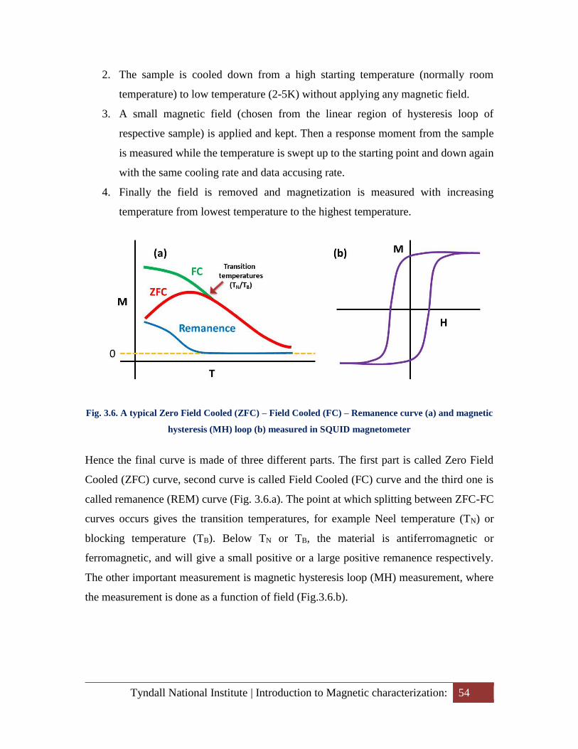
Tyndall National Institute | Introduction to Magnetic characterization: 54
2. The sample is cooled down from a high starting temperature (normally room
temperature) to low temperature (2-5K) without applying any magnetic field.
3. A small magnetic field (chosen from the linear region of hysteresis loop of
respective sample) is applied and kept. Then a response moment from the sample
is measured while the temperature is swept up to the starting point and down again
with the same cooling rate and data accusing rate.
4. Finally the field is removed and magnetization is measured with increasing
temperature from lowest temperature to the highest temperature.
Fig. 3.6. A typical Zero Field Cooled (ZFC) – Field Cooled (FC) – Remanence curve (a) and magnetic
hysteresis (MH) loop (b) measured in SQUID magnetometer
Hence the final curve is made of three different parts. The first part is called Zero Field
Cooled (ZFC) curve, second curve is called Field Cooled (FC) curve and the third one is
called remanence (REM) curve (Fig. 3.6.a). The point at which splitting between ZFC-FC
curves occurs gives the transition temperatures, for example Neel temperature (TN) or
blocking temperature (TB). Below TN or TB, the material is antiferromagnetic or
ferromagnetic, and will give a small positive or a large positive remanence respectively.
The other important measurement is magnetic hysteresis loop (MH) measurement, where
the measurement is done as a function of field (Fig.3.6.b).
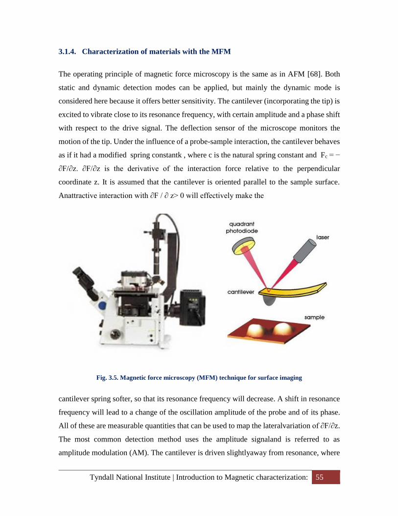
Tyndall National Institute | Introduction to Magnetic characterization: 55
3.1.4. Characterization of materials with the MFM
The operating principle of magnetic force microscopy is the same as in AFM [68]. Both
static and dynamic detection modes can be applied, but mainly the dynamic mode is
considered here because it offers better sensitivity. The cantilever (incorporating the tip) is
excited to vibrate close to its resonance frequency, with certain amplitude and a phase shift
with respect to the drive signal. The deflection sensor of the microscope monitors the
motion of the tip. Under the influence of a probe-sample interaction, the cantilever behaves
as if it had a modified spring constantk , where c is the natural spring constant and Fc = −
∂F/∂z. ∂F/∂z is the derivative of the interaction force relative to the perpendicular
coordinate z. It is assumed that the cantilever is oriented parallel to the sample surface.
Anattractive interaction with ∂F / ∂ z> 0 will effectively make the
Fig. 3.5. Magnetic force microscopy (MFM) technique for surface imaging
cantilever spring softer, so that its resonance frequency will decrease. A shift in resonance
frequency will lead to a change of the oscillation amplitude of the probe and of its phase.
All of these are measurable quantities that can be used to map the lateralvariation of ∂F/∂z.
The most common detection method uses the amplitude signaland is referred to as
amplitude modulation (AM). The cantilever is driven slightlyaway from resonance, where
Tyndall National Institute | Structural characterization of materials 56
the slope of the amplitude-versus-frequency curve is high, in order to maximize the signal
obtained from a given force derivative.Measurement sensitivity, or the minimum
detectable force derivative, has an inverse dependence on the Q value of the oscillating
system. Therefore, a high Qvalue might seem advantageous, but this has the drawback that
it increases theresponse time of the detection system. In the situations where Q is
necessarily high, for example when scanning in vacuum, a suitable alternative is the
frequency modulation (FM) technique. In this method the cantilever oscillates directly at
its resonance frequency by using a feedback amplifier with amplitude control.
The VFM2-HV AFM-MFM by Asylum Research has been used for different AFM-MFM
measuremnts in this thesis. The VFM2-HV can apply static magnetic fields up to ±0.8 T(~1
G resolution), parallel to the sample plane. A unique design incorporating rare-earth
magnets are used to produce the magnetic field. Due to this, there is no effect of heating or
drift during the change of the field which provides low-noise, high-precision scanning
probemeasurements. By rotating the powerful rare-earth magnet it allows the magnetic
field intensity variation at the sample (maximum field when rotated at 90°, field is turned
off at 0° or 180°). Once a field value is reached, the motor is turned off and the field is
remained without residual heat, thermal drift, or mechanical vibration during the
measurement time. Before any measurement, sharp MFM tips are magnetized by rare earth
permanent magnets.
3.2. Structural characterization of materials
3.2.1. Characterization of materials with the TEM
In Transmission Electron Microscopy (TEM) a monochromatic beam of electrons is
accelerated through a potential of 40 to 100 kilovolts (kV) and passed through a strong
magnetic field that acts as a lens [69]. Then this beam is transmitted through an ultra-thin
sample and it interacts with the material while passing through. An image is formed due to
the interaction of the electrons transmitted through the material which is magnified,
focused and detected by a sensor such as a CCD camera. The resolution of a modern TEM
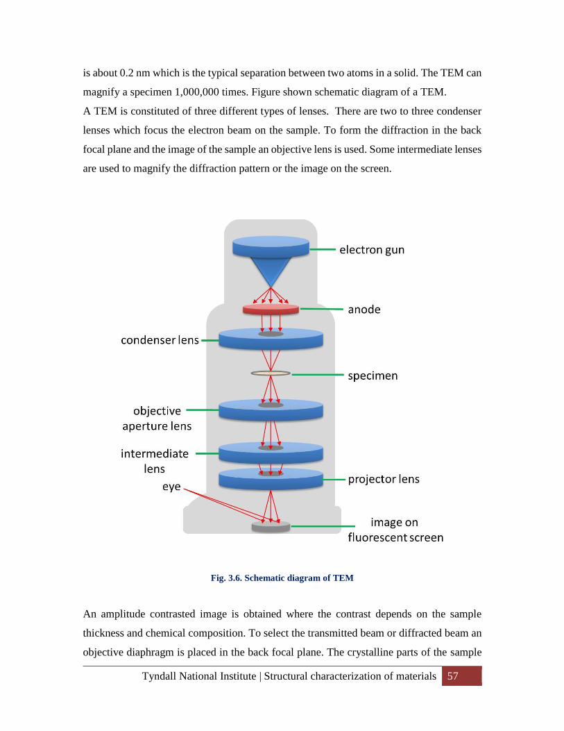
Tyndall National Institute | Structural characterization of materials 57
is about 0.2 nm which is the typical separation between two atoms in a solid. The TEM can
magnify a specimen 1,000,000 times. Figure shown schematic diagram of a TEM.
A TEM is constituted of three different types of lenses. There are two to three condenser
lenses which focus the electron beam on the sample. To form the diffraction in the back
focal plane and the image of the sample an objective lens is used. Some intermediate lenses
are used to magnify the diffraction pattern or the image on the screen.
Fig. 3.6. Schematic diagram of TEM
An amplitude contrasted image is obtained where the contrast depends on the sample
thickness and chemical composition. To select the transmitted beam or diffracted beam an
objective diaphragm is placed in the back focal plane. The crystalline parts of the sample
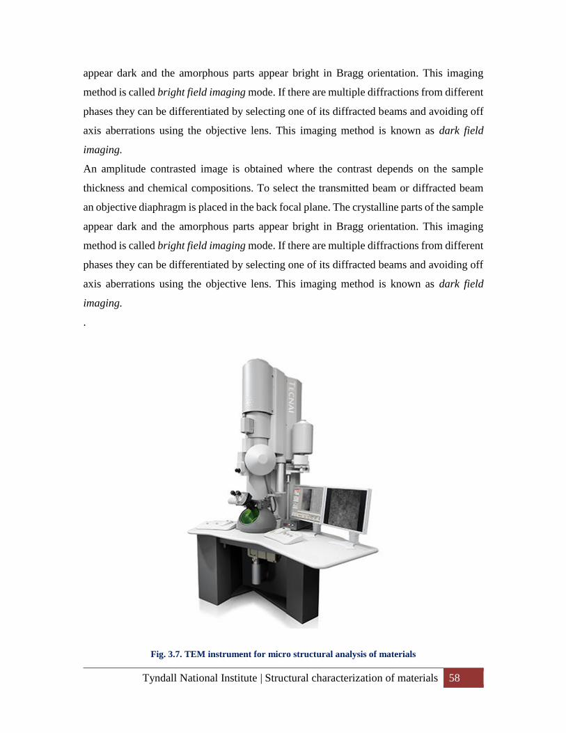
Tyndall National Institute | Structural characterization of materials 58
appear dark and the amorphous parts appear bright in Bragg orientation. This imaging
method is called bright field imaging mode. If there are multiple diffractions from different
phases they can be differentiated by selecting one of its diffracted beams and avoiding off
axis aberrations using the objective lens. This imaging method is known as dark field
imaging.
An amplitude contrasted image is obtained where the contrast depends on the sample
thickness and chemical compositions. To select the transmitted beam or diffracted beam
an objective diaphragm is placed in the back focal plane. The crystalline parts of the sample
appear dark and the amorphous parts appear bright in Bragg orientation. This imaging
method is called bright field imaging mode. If there are multiple diffractions from different
phases they can be differentiated by selecting one of its diffracted beams and avoiding off
axis aberrations using the objective lens. This imaging method is known as dark field
imaging.
.
Fig. 3.7. TEM instrument for micro structural analysis of materials
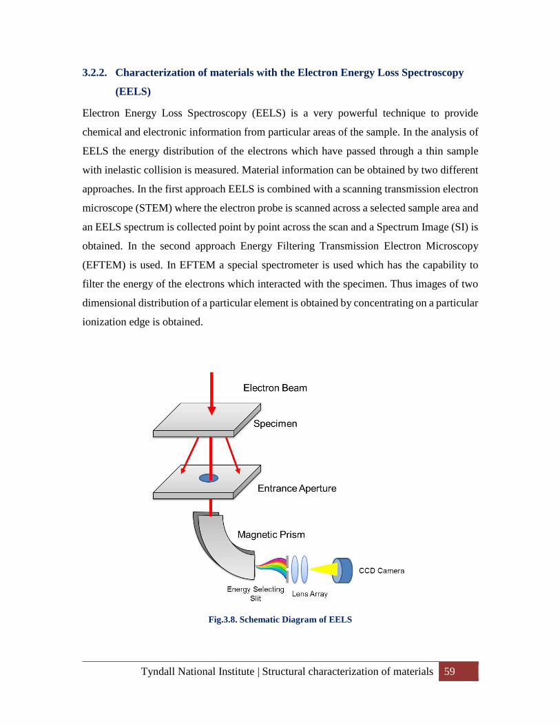
Tyndall National Institute | Structural characterization of materials 59
3.2.2. Characterization of materials with the Electron Energy Loss Spectroscopy
(EELS)
Electron Energy Loss Spectroscopy (EELS) is a very powerful technique to provide
chemical and electronic information from particular areas of the sample. In the analysis of
EELS the energy distribution of the electrons which have passed through a thin sample
with inelastic collision is measured. Material information can be obtained by two different
approaches. In the first approach EELS is combined with a scanning transmission electron
microscope (STEM) where the electron probe is scanned across a selected sample area and
an EELS spectrum is collected point by point across the scan and a Spectrum Image (SI) is
obtained. In the second approach Energy Filtering Transmission Electron Microscopy
(EFTEM) is used. In EFTEM a special spectrometer is used which has the capability to
filter the energy of the electrons which interacted with the specimen. Thus images of two
dimensional distribution of a particular element is obtained by concentrating on a particular
ionization edge is obtained.
Fig.3.8. Schematic Diagram of EELS
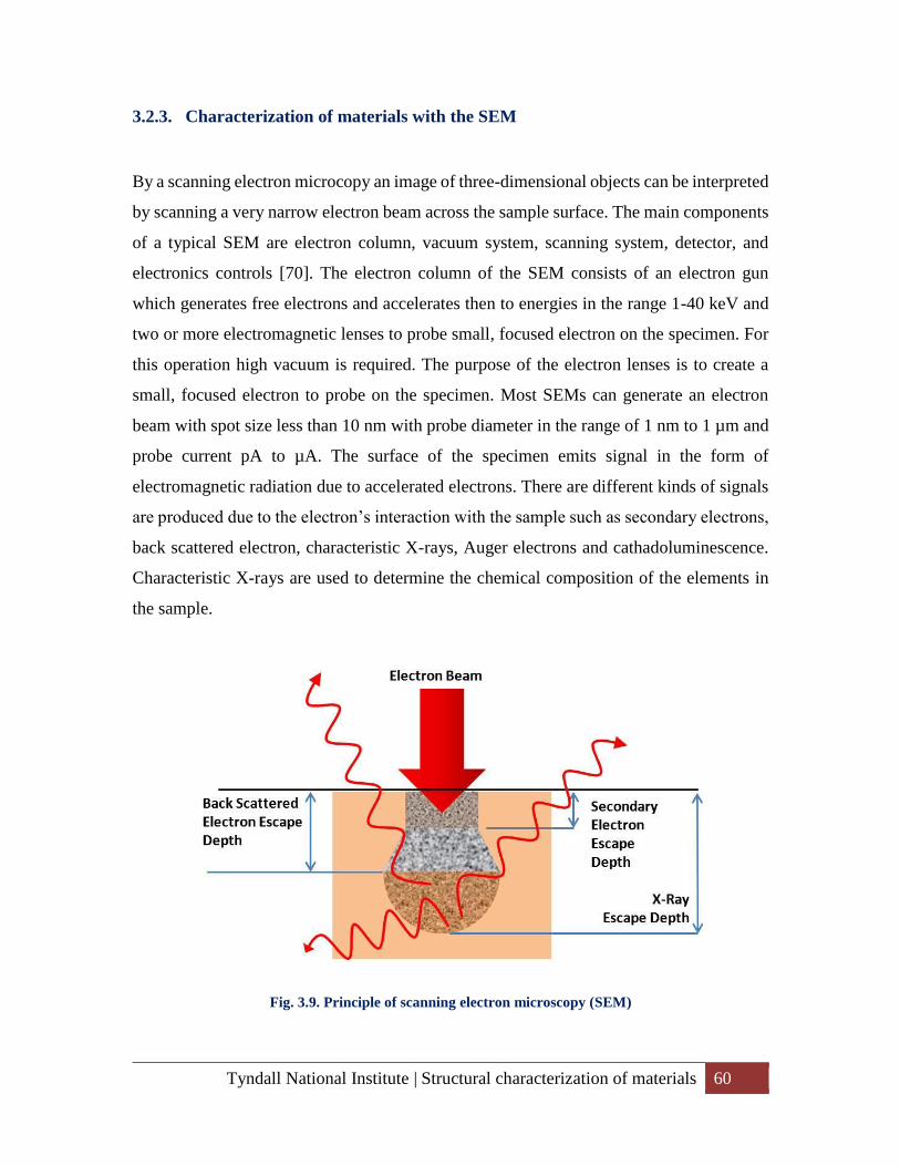
Tyndall National Institute | Structural characterization of materials 60
3.2.3. Characterization of materials with the SEM
By a scanning electron microcopy an image of three-dimensional objects can be interpreted
by scanning a very narrow electron beam across the sample surface. The main components
of a typical SEM are electron column, vacuum system, scanning system, detector, and
electronics controls [70]. The electron column of the SEM consists of an electron gun
which generates free electrons and accelerates then to energies in the range 1-40 keV and
two or more electromagnetic lenses to probe small, focused electron on the specimen. For
this operation high vacuum is required. The purpose of the electron lenses is to create a
small, focused electron to probe on the specimen. Most SEMs can generate an electron
beam with spot size less than 10 nm with probe diameter in the range of 1 nm to 1 µm and
probe current pA to µA. The surface of the specimen emits signal in the form of
electromagnetic radiation due to accelerated electrons. There are different kinds of signals
are produced due to the electron’s interaction with the sample such as secondary electrons,
back scattered electron, characteristic X-rays, Auger electrons and cathadoluminescence.
Characteristic X-rays are used to determine the chemical composition of the elements in
the sample.
Fig. 3.9. Principle of scanning electron microscopy (SEM)
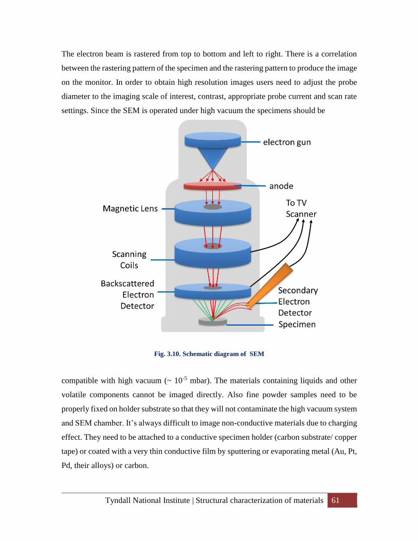
Tyndall National Institute | Structural characterization of materials 61
The electron beam is rastered from top to bottom and left to right. There is a correlation
between the rastering pattern of the specimen and the rastering pattern to produce the image
on the monitor. In order to obtain high resolution images users need to adjust the probe
diameter to the imaging scale of interest, contrast, appropriate probe current and scan rate
settings. Since the SEM is operated under high vacuum the specimens should be
Fig. 3.10. Schematic diagram of SEM
compatible with high vacuum (~ 10-5 mbar). The materials containing liquids and other
volatile components cannot be imaged directly. Also fine powder samples need to be
properly fixed on holder substrate so that they will not contaminate the high vacuum system
and SEM chamber. It’s always difficult to image non-conductive materials due to charging
effect. They need to be attached to a conductive specimen holder (carbon substrate/ copper
tape) or coated with a very thin conductive film by sputtering or evaporating metal (Au, Pt,
Pd, their alloys) or carbon.
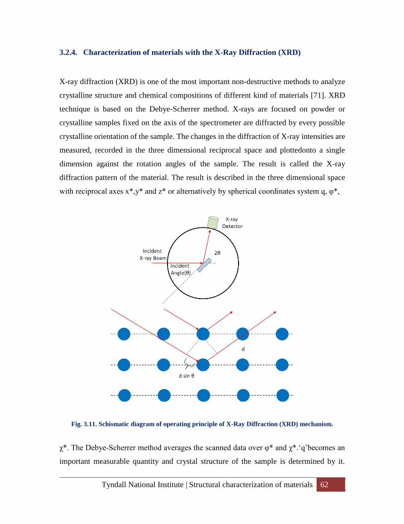
Tyndall National Institute | Structural characterization of materials 62
3.2.4. Characterization of materials with the X-Ray Diffraction (XRD)
X-ray diffraction (XRD) is one of the most important non-destructive methods to analyze
crystalline structure and chemical compositions of different kind of materials [71]. XRD
technique is based on the Debye-Scherrer method. X-rays are focused on powder or
crystalline samples fixed on the axis of the spectrometer are diffracted by every possible
crystalline orientation of the sample. The changes in the diffraction of X-ray intensities are
measured, recorded in the three dimensional reciprocal space and plottedonto a single
dimension against the rotation angles of the sample. The result is called the X-ray
diffraction pattern of the material. The result is described in the three dimensional space
with reciprocal axes x*,y* and z* or alternatively by spherical coordinates system q, φ*,
Fig. 3.11. Schismatic diagram of operating principle of X-Ray Diffraction (XRD) mechanism.
χ*. The Debye-Scherrer method averages the scanned data over φ* and χ*.‘q’becomes an
important measurable quantity and crystal structure of the sample is determined by it.
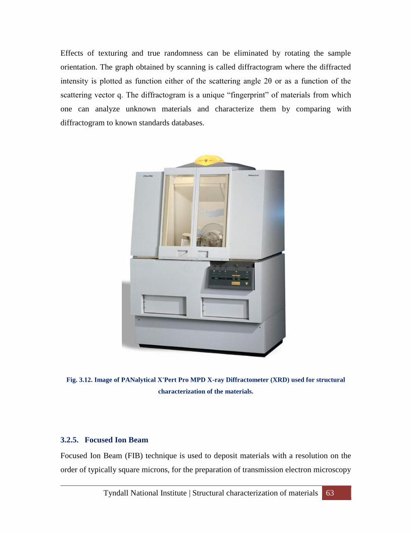
Tyndall National Institute | Structural characterization of materials 63
Effects of texturing and true randomness can be eliminated by rotating the sample
orientation. The graph obtained by scanning is called diffractogram where the diffracted
intensity is plotted as function either of the scattering angle 2θ or as a function of the
scattering vector q. The diffractogram is a unique “fingerprint” of materials from which
one can analyze unknown materials and characterize them by comparing with
diffractogram to known standards databases.
Fig. 3.12. Image of PANalytical X'Pert Pro MPD X-ray Diffractometer (XRD) used for structural
characterization of the materials.
3.2.5. Focused Ion Beam
Focused Ion Beam (FIB) technique is used to deposit materials with a resolution on the
order of typically square microns, for the preparation of transmission electron microscopy
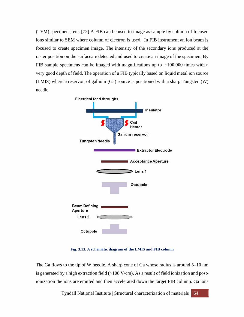
Tyndall National Institute | Structural characterization of materials 64
(TEM) specimens, etc. [72] A FIB can be used to image as sample by column of focused
ions similar to SEM where column of electron is used. In FIB instrument an ion beam is
focused to create specimen image. The intensity of the secondary ions produced at the
raster position on the surfaceare detected and used to create an image of the specimen. By
FIB sample specimens can be imaged with magnifications up to ∽100 000 times with a
very good depth of field. The operation of a FIB typically based on liquid metal ion source
(LMIS) where a reservoir of gallium (Ga) source is positioned with a sharp Tungsten (W)
needle.
Fig. 3.13. A schematic diagram of the LMIS and FIB column
The Ga flows to the tip of W needle. A sharp cone of Ga whose radius is around 5–10 nm
is generated by a high extraction field (>108 V/cm). As a result of field ionization and post-
ionization the ions are emitted and then accelerated down the target FIB column. Ga ions
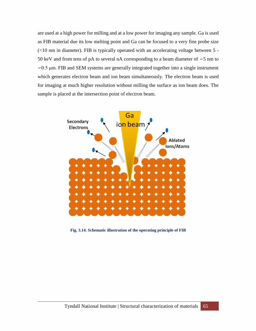
Tyndall National Institute | Structural characterization of materials 65
are used at a high power for milling and at a low power for imaging any sample. Ga is used
as FIB material due its low melting point and Ga can be focused to a very fine probe size
(<10 nm in diameter). FIB is typically operated with an accelerating voltage between 5 -
50 keV and from tens of pA to several nA corresponding to a beam diameter of ∽5 nm to
∽0.5 μm. FIB and SEM systems are generally integrated together into a single instrument
which generates electron beam and ion beam simultaneously. The electron beam is used
for imaging at much higher resolution without milling the surface as ion beam does. The
sample is placed at the intersection point of electron beam.
Fig. 3.14. Schematic illustration of the operating principle of FIB
Tyndall National Institute | Chapter - Micromagnetic Simulations 66
4. Chapter - Micromagnetic Simulations
4.1. Introduction
In this chapter the technique of micromagnetic simulation has been discussed. The
theoretical framework has been explained for the simulated results which have been
incorporated in chapter 5. Further the advantages and limitation of micromagnetic
simulation technique have also been explained.
4.2. Micromagnetic Theory
Presently there are different computational techniques available to model magnetic
phenomena of materials and their associated parameters. The micromagnetic modelling
predicts the behaviour of magnetic materials on the length scale of nano-metre to
micrometre by magnetization reversal process. When an external magnetic field is applied
to a sample the individual atoms try to align at a particular direction to minimize the energy
of the system. Depending on the material and sample structure energy configuration of the
system varies. Micromagnetic simulation method models all possible magnetic interaction
within the system and fully demonstrates the magnetic domain landscape’s evolution with
time. Micromagneic simulation is one level above atomic simulation used to describe
internal magnetic structure of a system.
4.3. Energy terms in micromagnetic simulation
Since micromagnetic simmulations is based on the magnetic interaction of individual
magnetic moments, a continuous magnetization M is used to approximate the minimum
energy.
i. Exchange energy:
One of the fundamental phenomenons of magnetism where individual atomic magnetic
moments try to align all other neighboring atomic magnetic moments within a material is
known as the exchange interaction (Aharoni, 2000). [73] The energy associated with this
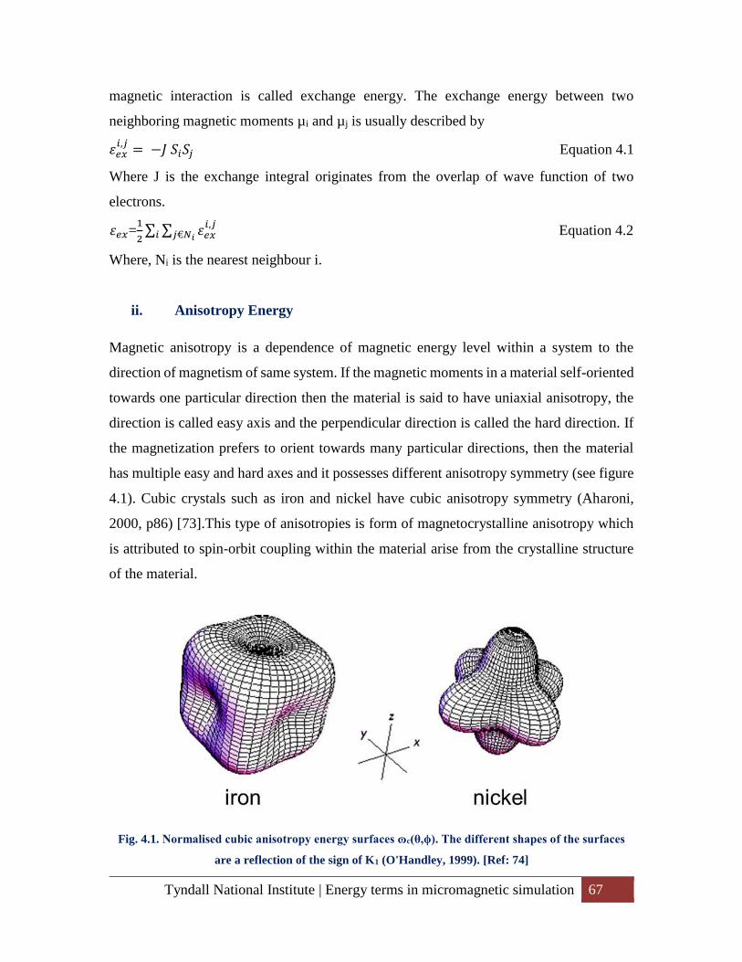
Tyndall National Institute | Energy terms in micromagnetic simulation 67
magnetic interaction is called exchange energy. The exchange energy between two
neighboring magnetic moments µi and µj is usually described by
휀𝑒𝑥𝑖,𝑗
= −𝐽 𝑆𝑖𝑆𝑗 Equation 4.1
Where J is the exchange integral originates from the overlap of wave function of two
electrons.
휀𝑒𝑥=1
2∑ ∑ 휀𝑒𝑥
𝑖,𝑗𝑗€𝑁𝑖𝑖 Equation 4.2
Where, Ni is the nearest neighbour i.
ii. Anisotropy Energy
Magnetic anisotropy is a dependence of magnetic energy level within a system to the
direction of magnetism of same system. If the magnetic moments in a material self-oriented
towards one particular direction then the material is said to have uniaxial anisotropy, the
direction is called easy axis and the perpendicular direction is called the hard direction. If
the magnetization prefers to orient towards many particular directions, then the material
has multiple easy and hard axes and it possesses different anisotropy symmetry (see figure
4.1). Cubic crystals such as iron and nickel have cubic anisotropy symmetry (Aharoni,
2000, p86) [73].This type of anisotropies is form of magnetocrystalline anisotropy which
is attributed to spin-orbit coupling within the material arise from the crystalline structure
of the material.
Fig. 4.1. Normalised cubic anisotropy energy surfaces ɷc(θ,ϕ). The different shapes of the surfaces
are a reflection of the sign of K1 (O'Handley, 1999). [Ref: 74]
Tyndall National Institute | Landau Lifshiftz Gilbert Equation 68
iii. Zeeman energy
When an external magnetic field (H) is applied to magnetic moment (µ) energy supplied
by the external field induces the rotation of internal magnetization of material by
harmonisation of the directions of internal and internal fields to minimization of Zeeman
energy:
휀𝑍𝑒𝑖 = −µ0µ𝑖. 𝐻𝑖 Equation 4.3
Where µ𝑖 and 𝐻𝑖 are the magnetization of individual magnetic moment due to the externally
applied magnetic field on it.
The Zeeman energy reaches a minimum when all the magnetic moments are aligned in a
particular direction due to the applied field.
iv. Dipolar energy
Dipolar energy often called magnetostatic or demagnetising energy associated with the
magnetic flux lines is the resultant energy due to the internal interaction of magnetic
moments. The dipolar energy for two magnetic moments µ𝑖. and µ𝑗 positioned at ri and rj
can be represented as:
휀𝑑𝑖𝑝𝑜𝑙𝑒𝑖,𝑗
= µ0 (µ𝑖.µ𝑗
|𝑟𝑖𝑗|3 −
3(µ𝑖𝑗.µ𝑖𝑗).(µ𝑗.µ𝑖𝑗)
|𝑟𝑖𝑗|5 ) Equation 4.4
Where 𝑟𝑖𝑗 = 𝑟𝑖-𝑟𝑗
In the presence of external magnetic field a demagnetization field Hde(r) is created in the
sample. The dipolar energy can be represented for a continuous media:
휀𝑑𝑖 = −µ0 ∫ 𝑯𝑑𝑒(𝒓). 𝑴(𝒓)𝑑3𝑟𝑣
Equation 4.5
4.4. Landau Lifshiftz Gilbert Equation
An important differential micromagnetic equation to describe the precession towards
equilibrium magnetization was derived by Landau and Lifshitz (1935). Later Gilbert (1955)
modified the equation adding an extra damping term which leads to the Landau-Lifshitz-
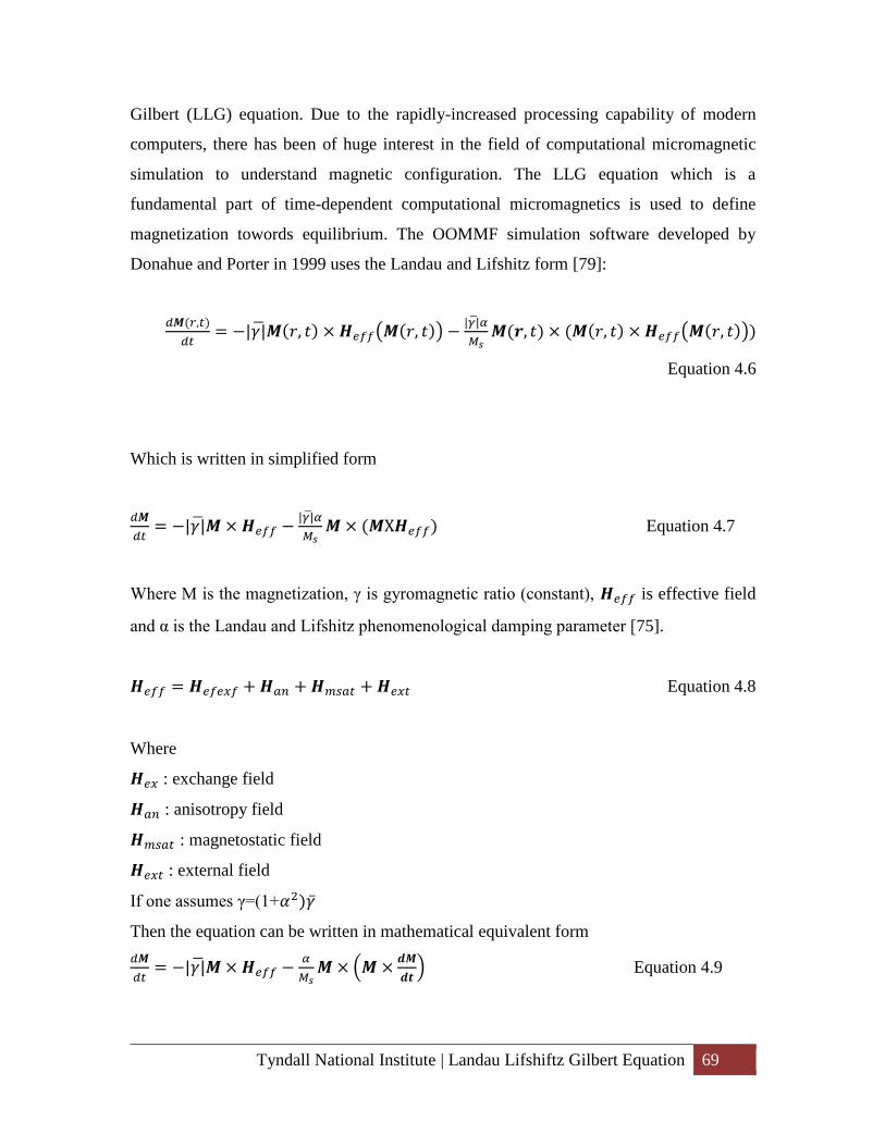
Tyndall National Institute | Landau Lifshiftz Gilbert Equation 69
Gilbert (LLG) equation. Due to the rapidly-increased processing capability of modern
computers, there has been of huge interest in the field of computational micromagnetic
simulation to understand magnetic configuration. The LLG equation which is a
fundamental part of time-dependent computational micromagnetics is used to define
magnetization towords equilibrium. The OOMMF simulation software developed by
Donahue and Porter in 1999 uses the Landau and Lifshitz form [79]:
𝑑𝑴(𝑟,𝑡)
𝑑𝑡= −|𝛾|𝑴(𝑟, 𝑡) × 𝑯𝑒𝑓𝑓(𝑴(𝑟, 𝑡)) −
|𝛾|𝛼
𝑀𝑠𝑴(𝒓, 𝑡) × (𝑴(𝑟, 𝑡) × 𝑯𝑒𝑓𝑓(𝑴(𝑟, 𝑡)))
Equation 4.6
Which is written in simplified form
𝑑𝑴
𝑑𝑡= −|𝛾|𝑴 × 𝑯𝑒𝑓𝑓 −
|𝛾|𝛼
𝑀𝑠𝑴 × (𝑴X𝑯𝑒𝑓𝑓) Equation 4.7
Where M is the magnetization, γ is gyromagnetic ratio (constant), 𝑯𝑒𝑓𝑓 is effective field
and α is the Landau and Lifshitz phenomenological damping parameter [75].
𝑯𝑒𝑓𝑓 = 𝑯𝑒𝑓𝑒𝑥𝑓 + 𝑯𝑎𝑛 + 𝑯𝑚𝑠𝑎𝑡 + 𝑯𝑒𝑥𝑡 Equation 4.8
Where
𝑯𝑒𝑥 : exchange field
𝑯𝑎𝑛 : anisotropy field
𝑯𝑚𝑠𝑎𝑡 : magnetostatic field
𝑯𝑒𝑥𝑡 : external field
If one assumes γ=(1+𝛼2)
Then the equation can be written in mathematical equivalent form
𝑑𝑴
𝑑𝑡= −|𝛾|𝑴 × 𝑯𝑒𝑓𝑓 −
𝛼
𝑀𝑠𝑴 × (𝑴 ×
𝒅𝑴
𝒅𝒕) Equation 4.9
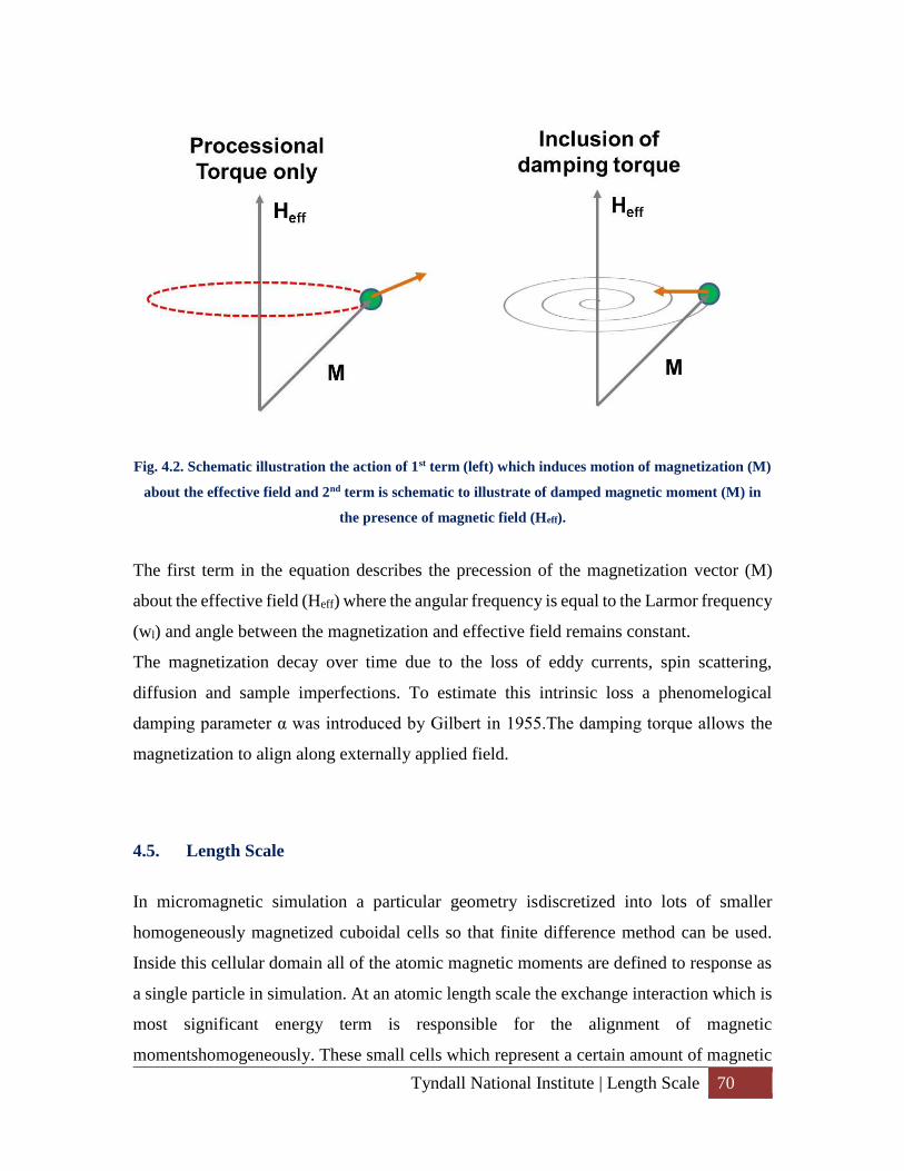
Tyndall National Institute | Length Scale 70
Fig. 4.2. Schematic illustration the action of 1st term (left) which induces motion of magnetization (M)
about the effective field and 2nd term is schematic to illustrate of damped magnetic moment (M) in
the presence of magnetic field (Heff).
The first term in the equation describes the precession of the magnetization vector (M)
about the effective field (Heff) where the angular frequency is equal to the Larmor frequency
(wl) and angle between the magnetization and effective field remains constant.
The magnetization decay over time due to the loss of eddy currents, spin scattering,
diffusion and sample imperfections. To estimate this intrinsic loss a phenomelogical
damping parameter α was introduced by Gilbert in 1955.The damping torque allows the
magnetization to align along externally applied field.
4.5. Length Scale
In micromagnetic simulation a particular geometry isdiscretized into lots of smaller
homogeneously magnetized cuboidal cells so that finite difference method can be used.
Inside this cellular domain all of the atomic magnetic moments are defined to response as
a single particle in simulation. At an atomic length scale the exchange interaction which is
most significant energy term is responsible for the alignment of magnetic
momentshomogeneously. These small cells which represent a certain amount of magnetic
Tyndall National Institute | Length Scale 71
material can then be used to perform the simulation. For micromagnetic simulation a
smaller cell size is more desirable, particularly when there is curved surface in the sample
geometry.
The exchange length is a length scale over which the magnetization direction does not
change significantly. Due to the energy minimization of magnetostatic energy sample is
broken into multiple domains with different magnetisation directions. In a coarse mesh
micromagnetic software cannot resolve the exchange length properly and independent
domains will not form correctly. Hence, the magnetisation can change direction over one
domain wall width as given by following equation:
𝛿𝐵 = 𝜋√𝐴
𝐾 Equation 4.10
The exchange length is calculated by considering (Seberino and Bertram, 2001,
Kronmüller and Fähnle, 2003)[76, 77]:
𝜆𝑒𝑥√𝐴
1
2µ0𝑀𝑠
2 Equation 4.11
Where A is the exchange energy, µ0 is the magnetic constant and MS is the magnetisation,
µ0the magnetic constant. Therefor exchange length 𝜆𝑒𝑥 gives us a quantitative assumption
of mesh resolution required for micromagnetic simulation.
Fig.4.3. The effect of cell size and number of cell for a sample of sphere shape. As the cell size is
reduced the ‘model’ gives much more accurate ‘spherical’ representation and accuracy of the
simulation result is also increased. [Ref: Richard Boardman’s PhD thesis, University of
Southampton][Ref: 78]
Tyndall National Institute | Length Scale 72
In general one equation of motion is solved for each cell. By reducing the cell size the
number of cell is rapidly increased and simultaneously the computational overhead is also
increased. The accuracy of simulation is also increased with the increment of number of
cells shown in Figure 4.3. The demagnetization field Hd at each cell depends on the
magnetization distribution over the entire mesh due to external applied field.
4.6. The Object Oriented MicroMagnetic Framework (OOMMF)
In micromagnetic simulation a set of partial differential equations are repetitively solved.
For the systems where static metastable magnetisation state is considered can be simply
relaxed by defining some initial magnetisation configuration, generally homogeneous or
random. Then the Landau-Lifshitz-Gilbert equation is used as the Finite Differentiate (FD)
method, opposed to Finite Element (FE) method to iterate the system until the rate of
change of magnetisation goes below a certain threshold. The LLG theory which is difficult
to solve analytically is numerically solved over time and leads to a set of differential
equations. To solve that freely available Object Oriented Micromagnetic Framework
(OOMMF) program based on FD method is used. [79]OOMMF was developed by
Donahue and Porter in 1999 and provided by the National Institute of Standards and
Technology (NIST), an agency of the U.S. Department of Commerce [79]. OOMMF has
been exclusively used for all micromagnetic simulation for this thesis. To run OOMMF
Tcl/Tk package is also required (Ball, 1999, Flynt, 1999, Raines and Tranter, 1999, Smith,
2000, Welch, 1999). There are few computational issues involved with OOMMF
simulation. OOMMF consumes approximately one kilobyte of RAM. The simulation
packagewhich must be loaded into RAM itself requires certain amount of RAM and creates
a fixed overhead. Figure 4.4 shows the amount of memory (RAM) required for simulation
as function cell geometry.
The first stage in the OOMMF simulation process is to define the magnetic structure to be
solved. This is done by creating a MIF file which contains the material parameters, defines
the structural geometry. The experimental parameters over which the simulation runs also
defined in MIF file. It is essential to use accurate material parameters as inputs which are
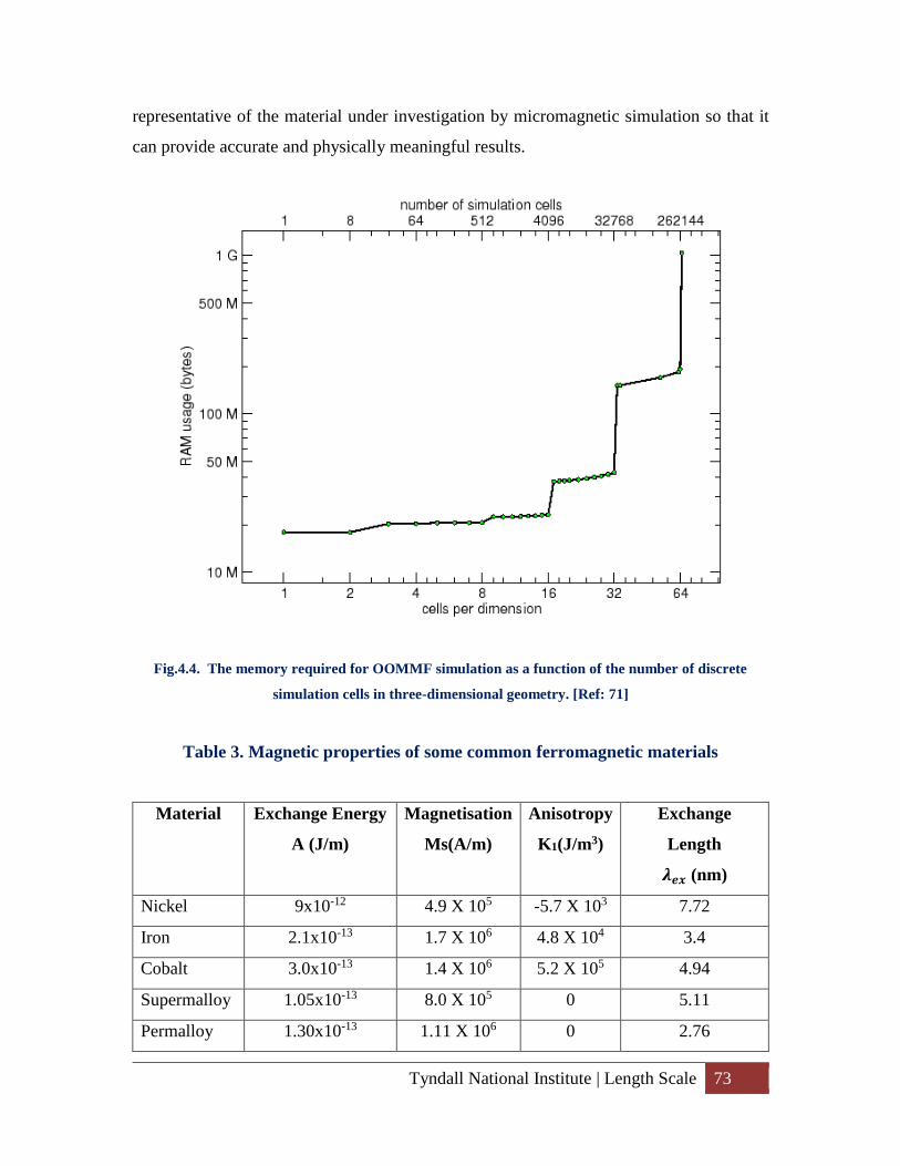
Tyndall National Institute | Length Scale 73
representative of the material under investigation by micromagnetic simulation so that it
can provide accurate and physically meaningful results.
Fig.4.4. The memory required for OOMMF simulation as a function of the number of discrete
simulation cells in three-dimensional geometry. [Ref: 71]
Table 3. Magnetic properties of some common ferromagnetic materials
Material Exchange Energy
A (J/m)
Magnetisation
Ms(A/m)
Anisotropy
K1(J/m3)
Exchange
Length
𝝀𝒆𝒙 (nm)
Nickel 9x10-12 4.9 X 10⁵ -5.7 X 10³ 7.72
Iron 2.1x10⁻¹³ 1.7 X 10⁶ 4.8 X 10⁴ 3.4
Cobalt 3.0x10⁻¹³ 1.4 X 10⁶ 5.2 X 10⁵ 4.94
Supermalloy 1.05x10⁻¹³ 8.0 X 10⁵ 0 5.11
Permalloy 1.30x10⁻¹³ 1.11 X 10⁶ 0 2.76

Tyndall National Institute | Length Scale 74
Ms= Saturation magnetisation in A/m
K1=First anisotropy constant in J/m3, i.e. by first order approximation the uniaxial
anisotropy is given by K1Vsin2θ and 𝐾1 =µ0𝑀𝑠𝐻𝑘
2
A=3𝑘𝐵𝑇𝑐
𝑎𝑍; kB is Boltzman’s Constant, Tc is the Curie temperature, a is lattice constant and
z is number of nearest neighbouring atoms.
Tyndall National Institute | Chapter – Manipulation of magnetic anisotropy-
shape/dipolar
75
5 Chapter – Manipulation of magnetic anisotropy-shape/dipolar
5.1. Introduction
One of the most significant challenges in micromagnetic devices is to configure
magnetization directions of patterned ferromagnetic films. In polycrystalline materials this
is mainly determined by external environmental effects or geometry [80] due to insufficient
long range microscopic crystalline order. Hence, applications of these materials are widely
based on the ability to control the magnetic anisotropy resulting out of spin configuration
based on pattern geometry. In recent years, this has been demonstrated for patterned,
isolated magnetic structures [81-84] and structured continuous magnetic films [85]. Such
kinds of control open up opportunities for potential applications such as spintronic devices,
magnetic random access memory (MRAM)[86] high density patterned information storage
media[86,87], and high precision ultra small magnetic field sensors[88]. Due to
fundamental reasons and potential applications, it is necessary to understand further the
magnetic properties of patterned structures in reduced dimensions, while both geometry
and crystal microstructure are needed to be optimised prior to configure the
magnetization[89]. Subsequent investigations further reveal properties like geometrical
frustration, domain wall pining, etc due to dipolar interaction based on spin configurations
[90, 91]. Several methods such as ion irradiation through a mask, selective epitaxy, surface
modulation [92], etc. have been studied to control the magnetization configuration in
patterned structures. Among them, surface nanomodulation is preferred for its cost
effectiveness and simplicity to engineer the spin configuration locally [93]. Furthermore,
the optimization of magnetic parameters such as pattern geometry, film thickness, intrinsic
anisotropy, and coercivity is essential to obtain a controlled anisotropy in a film by
nanomodulation. Magnetostatic energy induced by strong nanomodulation forces the spins
into local vortices which is unfavourable for many applications. Thus, the development of
a physical model for an optimized modulation is essential to manipulate the film
anisotropy.
In the present work results of anisotropy variation due to magnetic dipoles formation in
nanomodulated film and detailed micromagnetic simulation study with key symmetry
Tyndall National Institute | Introduction 76
features of complete nanomodulation based anisotropy in continuous ferromagnetic thin
films have been discussed. Novel ways to produce different anisotropy are introduced,
which have been validated by experimental evidences and analytical derivation. To
determine anisotropy variation due to the magnetostatic dipole interactions we performed
various magnetometry measurements combined with MFM imaging on nanomodulated
continuous Ni45Fe55 film. Artificially created ordered corrugation produces controllable
magnetic dipoles. However, while the external field favors such magnetic dipole alignment,
interdipole magnetostatic interaction results in a variation of the effective magnetostatic
energy in different directions. This effect translates into in-plane and out of plane
anisotropy variation depending upon modulation geometry.
It is also demonstrated how a unique nanostrucuture of continuous ferromagnetic film can
induce magnetic dipoles at sub-micron scale at pre-defined locations and play a key role to
tune the global magnetic properties of the film due to magnetostatic interactions. Synthetic
arrays of magnetic dipoles are tuneable at in-plane and out of plane directions and can be
rotated in plane in such three dimensional modulated structure. In-plane magnetic field
rotations influence magnetostatic interactions in different directions which open up a new
methodology to control the various magnetic properties of a ferromagnetic thin film.
Gradual formation of magnetic dipoles and their tunability have been studied in detail by
MFM imaging and other magnetic measurements. It is observed that the diploes go through
a transformation from metastable to stable state. The magnetostatic interaction depends on
their geometrical arrangements. Thus magnetic properties of the continuous film can be
varied by pattern geometry. This has been shown by experiment and micromagnetic
simulation (OOMMF) in nanomodulated Ni45Fe55. It is usual that in nano pattern bigger
than single magnetic domain, the dipole tries to form vortex at remanence state. Whereas
this unique three dimensional structure prevents vortex formation due to strong
magnetostatic interaction as a novel observation. Again this could influence the dynamic
properties of the thin film. A detail analytical study of dipolar energy for our system agrees
with our experimental and simulated results.
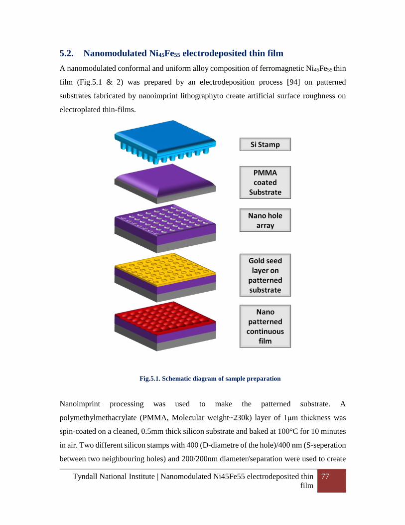
Tyndall National Institute | Nanomodulated Ni45Fe55 electrodeposited thin
film
77
5.2. Nanomodulated Ni45Fe55 electrodeposited thin film
A nanomodulated conformal and uniform alloy composition of ferromagnetic Ni45Fe55 thin
film (Fig.5.1 & 2) was prepared by an electrodeposition process [94] on patterned
substrates fabricated by nanoimprint lithographyto create artificial surface roughness on
electroplated thin-films.
Fig.5.1. Schematic diagram of sample preparation
Nanoimprint processing was used to make the patterned substrate. A
polymethylmethacrylate (PMMA, Molecular weight~230k) layer of 1μm thickness was
spin-coated on a cleaned, 0.5mm thick silicon substrate and baked at 100°C for 10 minutes
in air. Two different silicon stamps with 400 (D-diametre of the hole)/400 nm (S-seperation
between two neighbouring holes) and 200/200nm diameter/separation were used to create
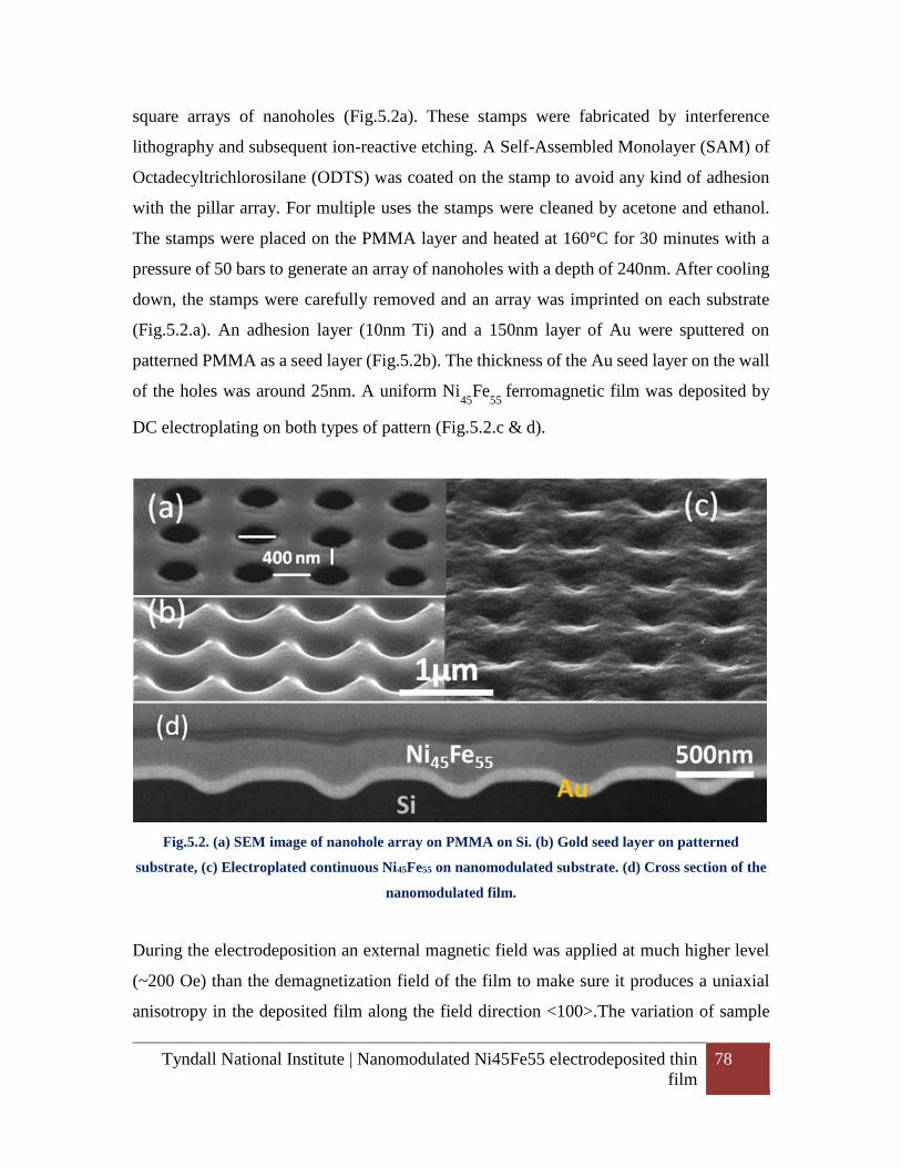
Tyndall National Institute | Nanomodulated Ni45Fe55 electrodeposited thin
film
78
square arrays of nanoholes (Fig.5.2a). These stamps were fabricated by interference
lithography and subsequent ion-reactive etching. A Self-Assembled Monolayer (SAM) of
Octadecyltrichlorosilane (ODTS) was coated on the stamp to avoid any kind of adhesion
with the pillar array. For multiple uses the stamps were cleaned by acetone and ethanol.
The stamps were placed on the PMMA layer and heated at 160°C for 30 minutes with a
pressure of 50 bars to generate an array of nanoholes with a depth of 240nm. After cooling
down, the stamps were carefully removed and an array was imprinted on each substrate
(Fig.5.2.a). An adhesion layer (10nm Ti) and a 150nm layer of Au were sputtered on
patterned PMMA as a seed layer (Fig.5.2b). The thickness of the Au seed layer on the wall
of the holes was around 25nm. A uniform Ni45
Fe55
ferromagnetic film was deposited by
DC electroplating on both types of pattern (Fig.5.2.c & d).
Fig.5.2. (a) SEM image of nanohole array on PMMA on Si. (b) Gold seed layer on patterned
substrate, (c) Electroplated continuous Ni45Fe55 on nanomodulated substrate. (d) Cross section of the
nanomodulated film.
During the electrodeposition an external magnetic field was applied at much higher level
(~200 Oe) than the demagnetization field of the film to make sure it produces a uniaxial
anisotropy in the deposited film along the field direction <100>.The variation of sample
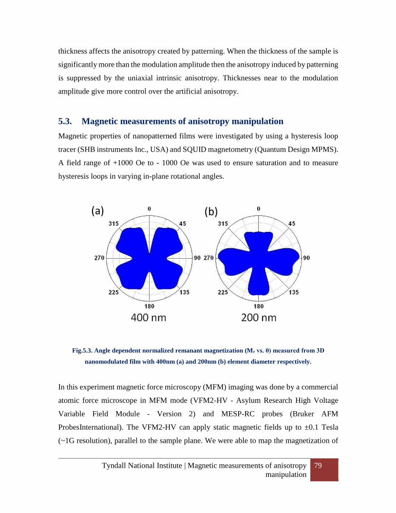
Tyndall National Institute | Magnetic measurements of anisotropy
manipulation
79
thickness affects the anisotropy created by patterning. When the thickness of the sample is
significantly more than the modulation amplitude then the anisotropy induced by patterning
is suppressed by the uniaxial intrinsic anisotropy. Thicknesses near to the modulation
amplitude give more control over the artificial anisotropy.
5.3. Magnetic measurements of anisotropy manipulation
Magnetic properties of nanopatterned films were investigated by using a hysteresis loop
tracer (SHB instruments Inc., USA) and SQUID magnetometry (Quantum Design MPMS).
A field range of +1000 Oe to - 1000 Oe was used to ensure saturation and to measure
hysteresis loops in varying in-plane rotational angles.
Fig.5.3. Angle dependent normalized remanant magnetization (Mr vs. θ) measured from 3D
nanomodulated film with 400nm (a) and 200nm (b) element diameter respectively.
In this experiment magnetic force microscopy (MFM) imaging was done by a commercial
atomic force microscope in MFM mode (VFM2-HV - Asylum Research High Voltage
Variable Field Module - Version 2) and MESP-RC probes (Bruker AFM
ProbesInternational). The VFM2-HV can apply static magnetic fields up to ±0.1 Tesla
(~1G resolution), parallel to the sample plane. We were able to map the magnetization of
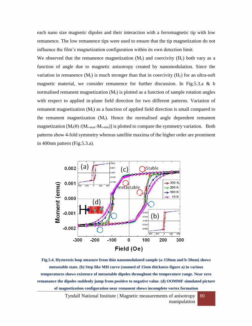
Tyndall National Institute | Magnetic measurements of anisotropy
manipulation
80
each nano size magnetic dipoles and their interaction with a ferromagnetic tip with low
remanence. The low remanence tips were used to ensure that the tip magnetization do not
influence the film’s magnetization configuration within its own detection limit.
We observed that the remanence magnetization (Mr) and coercivity (Hc) both vary as a
function of angle due to magnetic anisotropy created by nanomodulation. Since the
variation in remanence (Mr) is much stronger than that in coercivity (Hc) for an ultra-soft
magnetic material, we consider remanence for further discussion. In Fig.5.3.a & b
normalised remanent magnetization (Mr) is plotted as a function of sample rotation angles
with respect to applied in-plane field direction for two different patterns. Variation of
remanent magnetization (Mr) as a function of applied field direction is small compared to
the remanent magnetization (Mr). Hence the normalised angle dependent remanent
magnetization [Mr(θ) /(Mr-max-Mr-min)] is plotted to compare the symmetry variation. Both
patterns show 4-fold symmetry whereas satellite maxima of the higher order are prominent
in 400nm pattern (Fig.5.3.a).
Fig.5.4. Hysteresis loop measure from thin nanomodulated sample (a-150nm and b-50nm) shows
metastable state. (b) Step like MH curve (zoomed of 15nm thickness-figure a) in various
temperatures shows existence of metastable dipoles throughout the temperature range. Near zero
remanance the dipoles suddenly jump from positive to negative value. (d) OOMMF simulated picture
of magnetization configuration near remanent shows incomplete vortex formation
Tyndall National Institute | Magnetic measurements of anisotropy
manipulation
81
The anisotropy based on nanomodulation is so strong that it could dominate film’s uniaxial
anisotropy. A novel phase shift is observed in 200 nm pattern (Fig5.3.b) for higher aspect
ratio, whereas after gold deposition the aspect ratio diameter/separation (D/S) becomes 3:1.
The reason of this phase shift has been explained later. In the case of the thickness (t) of
the sample being significantly more than the modulation amplitude (A), the anisotropy
induced by patterning is dominated by the uniaxial intrinsic anisotropy of the film. When
sample thickness, t, ~150 nm is lower than modulation amplitude, A, (~ 240 nm) it tries to
form a vortex and a step like behaviour in MH curve is visible (Fig5.4.a) due to the effect
of nanomudulation . A further decrease in sample thickness (t) to ~50nm (Fig5.4.c) gives
near zero remanence. The sample with thickness (t) ~ 150nm was measured at different
temperatures (Fig5.4.c), which shows the existence of metastable states trough out the
temperature range. It is found that the nanomodulated film requires a very high field to
obtain saturation magnetization due to the formation of magnetic dipoles and their strong
coupling. For the change of external magnetic field the magnetic dipole goes through a
transition from saturation magnetization or stable non-hysteretic region via metastable
planar region to unstable dipolar state or jumps (Fig5.4.c). At near zero fields, the
remanence (Mr) suddenly jumps from positive to negative magnetization which indicates
the existence of magnetic dipoles with nonzero Mr. Thus a complete vortex cannot be
achieved in this unique structure. To understand the phenomena we focus on single
element. For a square array-pattern of 400 nm diameter and 100 nm modulation amplitude
( D/S is 1), the calculated energy densities are 0.49 x 10⁴ J /m3 and 1.33 x 10⁴ J /m3, for
vortex and near single domain state respectively. Since the energy of a vortex state is less
than that of a near-single-domain remanent state there should be a strong inclination to
adopt vortex states in the nanomodulated continuous ferromagnetic thin films. On the other
hand, it is necessary that the demagnetization processes needs to overcome the higher
energy barrier to create local vortex in nanomodulated continuous ferromagnetic thin films
where spins are strongly exchanged in parallel due to magnetostatic interaction. Thus these
magnetostatic interactions in this patterned matrix try to resist formation of vortices which
is analogous to closely-packed magnetic dots [95]. As a consequence, a near-single domain
state originates at the remanence magnetisation state with an intention to become a vortex
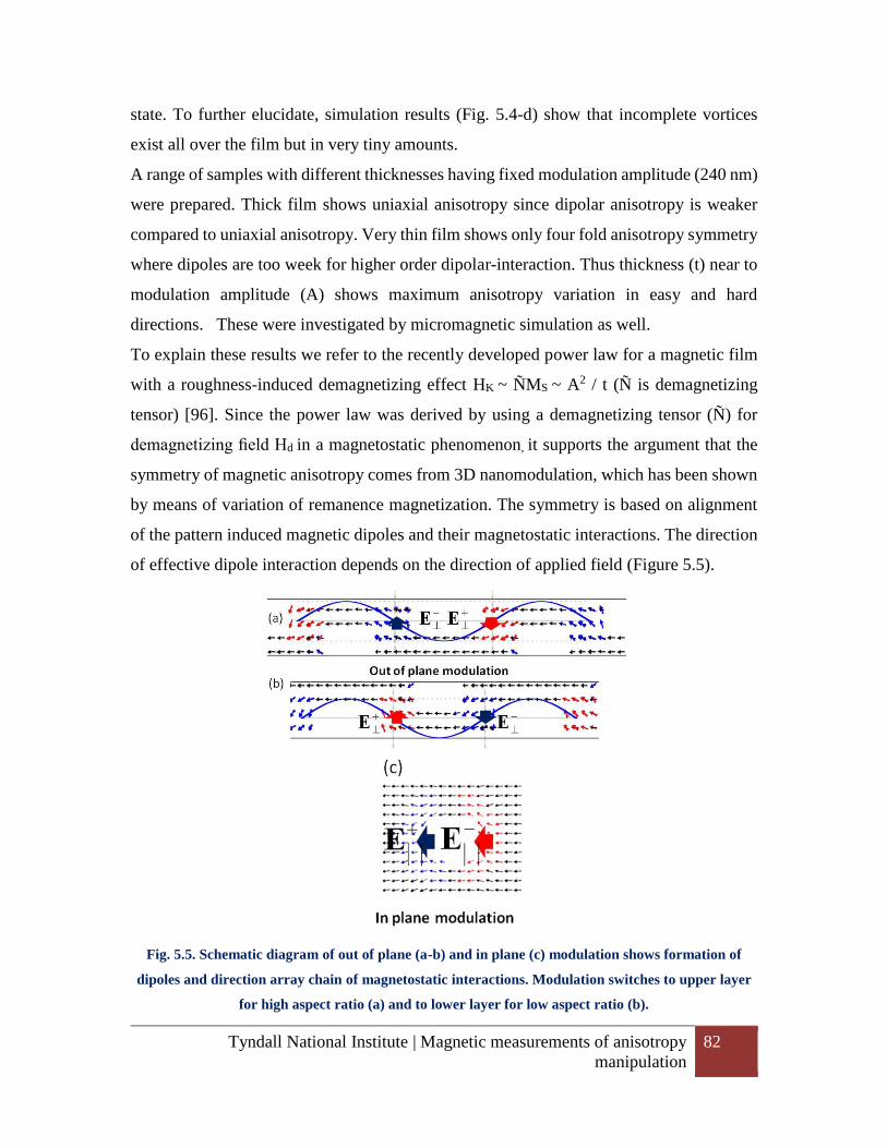
Tyndall National Institute | Magnetic measurements of anisotropy
manipulation
82
state. To further elucidate, simulation results (Fig. 5.4-d) show that incomplete vortices
exist all over the film but in very tiny amounts.
A range of samples with different thicknesses having fixed modulation amplitude (240 nm)
were prepared. Thick film shows uniaxial anisotropy since dipolar anisotropy is weaker
compared to uniaxial anisotropy. Very thin film shows only four fold anisotropy symmetry
where dipoles are too week for higher order dipolar-interaction. Thus thickness (t) near to
modulation amplitude (A) shows maximum anisotropy variation in easy and hard
directions. These were investigated by micromagnetic simulation as well.
To explain these results we refer to the recently developed power law for a magnetic film
with a roughness-induced demagnetizing effect HK ~ ÑMS ~ A2 / t (Ñ is demagnetizing
tensor) [96]. Since the power law was derived by using a demagnetizing tensor (Ñ) for
demagnetizing field Hd in a magnetostatic phenomenon, it supports the argument that the
symmetry of magnetic anisotropy comes from 3D nanomodulation, which has been shown
by means of variation of remanence magnetization. The symmetry is based on alignment
of the pattern induced magnetic dipoles and their magnetostatic interactions. The direction
of effective dipole interaction depends on the direction of applied field (Figure 5.5).
Fig. 5.5. Schematic diagram of out of plane (a-b) and in plane (c) modulation shows formation of
dipoles and direction array chain of magnetostatic interactions. Modulation switches to upper layer
for high aspect ratio (a) and to lower layer for low aspect ratio (b).
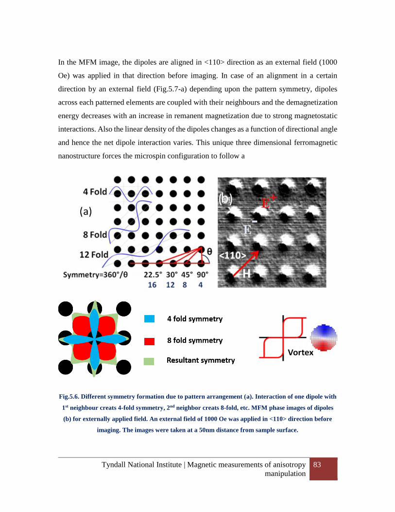
Tyndall National Institute | Magnetic measurements of anisotropy
manipulation
83
In the MFM image, the dipoles are aligned in <110> direction as an external field (1000
Oe) was applied in that direction before imaging. In case of an alignment in a certain
direction by an external field (Fig.5.7-a) depending upon the pattern symmetry, dipoles
across each patterned elements are coupled with their neighbours and the demagnetization
energy decreases with an increase in remanent magnetization due to strong magnetostatic
interactions. Also the linear density of the dipoles changes as a function of directional angle
and hence the net dipole interaction varies. This unique three dimensional ferromagnetic
nanostructure forces the microspin configuration to follow a
Fig.5.6. Different symmetry formation due to pattern arrangement (a). Interaction of one dipole with
1st neighbour creats 4-fold symmetry, 2nd neighbor creats 8-fold, etc. MFM phase images of dipoles
(b) for externally applied field. An external field of 1000 Oe was applied in <110> direction before
imaging. The images were taken at a 50nm distance from sample surface.
Tyndall National Institute | Micromagnetic simulation for anisotropy
manipulation
84
wave like propagation of magnetization which collectively generates in plane and out of
plane dipoles (Figure 5.5.a-c). In a square array of magnetic nano structure the magnetic
ordering is determined by minimization of collective magnetostatic energy whereas the
magnetic anisotropy energy depends on the dipole interaction if it is strong enough to keep
the magnetization after removal of applied field. Normally, the isolated nanostructure
bigger than single domain, tries to form vortex (Fig.5.6) at remanence state to obtain the
minimum energy state. Here the competition between two different dipoles (in plane and
out of plane) and possible spin pinning between two consecutive dipoles through
continuous ferromagnetic media keeps the magnetization stable at the direction of applied
field and resists vortex formation. We varied the angle of applied field direction with
respect to patterned array. The dipoles rotate with the rotation of applied field which is
shown in Figure 5.6 a. The variation of magnetic anisotropy was investigated by measuring
coersivity at different direction which shows a clear trend of four fold anisotropy symmetry
(Figure 5.3) in the square array structure. This result agrees with micromagnetic simulation
result. The competition between two different dipoles generates a collective metastable
magnetic configuration and a step like MH curve is observed (Figure 5.4). The wave pattern
creates a strong out of plane dipoles which becomes difficult to align at a particular in plane
direction by a high external field. This has been observed in measured MH curve. The
curve shows a prominent minor loop (Figure 5.4.c) and an unsaturated major loop (Figure
5.4.b) due to these strong out of plane dipoles. We applied a field of 1000 Oe, which is
large enough to saturate Ni45Fe55 film and map the magnetization of our patterned field
very carefully. Interestingly, a magnetic vortex with a single vortex core has been observed
at the center of each nanopattern at high field due to the gyration motion of out of plane
magnetic spins at vortex core.
5.4. Micromagnetic simulation for anisotropy manipulation
The experimental results for nanomodulated continuous ferromagnetic thin film has further
been investigated by static micromagnetic simulations which were carried out by solving
the Landau-Lifshitz-Gilbert (LLG) equations (Eqn. 5.12), using Object Oriented Micro-
magnetic Framework (OOMMF) [79] software from NIST US.
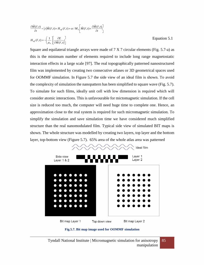
Tyndall National Institute | Micromagnetic simulation for anisotropy
manipulation
85
t
trMtrMMtrHtrM
t
trMSeff
),(),(/),(),(
),(
),(
1),(
0 trM
EtrH eff
Equation 5.1
Square and equilateral triangle arrays were made of 7 X 7 circular elements (Fig. 5.7-a) as
this is the minimum number of elements required to include long range magnetostatic
interaction effects in a large scale [97]. The real topographically patterned nanostructured
film was implemented by creating two consecutive atlases or 3D geometrical spaces used
for OOMMF simulation. In Figure 5.7 the side view of an ideal film is shown. To avoid
the complexity of simulation the nanopattern has been simplified to square wave (Fig. 5.7).
To simulate for such films, ideally unit cell with low dimension is required which will
consider atomic interactions. This is unfavourable for mictomagnetic simulation. If the cell
size is reduced too much, the computer will need huge time to complete one. Hence, an
approximation close to the real system is required for such micromagnetic simulation. To
simplify the simulation and save simulation time we have considered much simplified
structure than the real nanomodulated film. Typical side view of simulated BIT maps is
shown. The whole structure was modelled by creating two layers, top layer and the bottom
layer, top-bottom view (Figure 5.7). 65% area of the whole atlas area was patterned
Fig.5.7. Bit map image used for OOMMF simulation
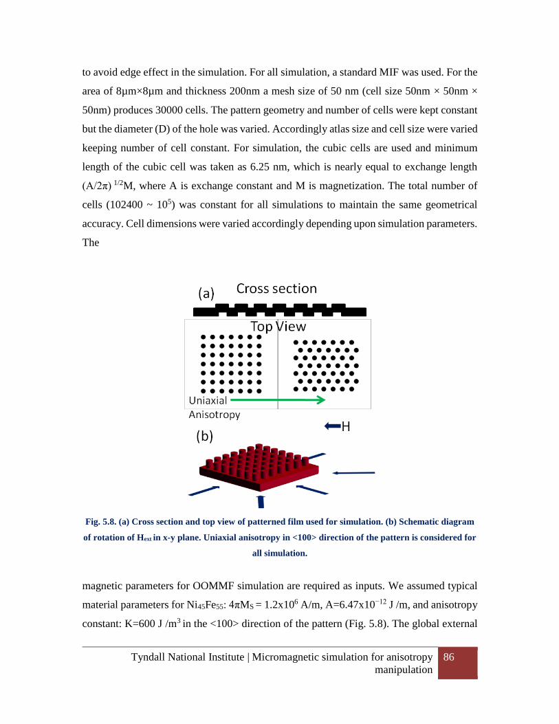
Tyndall National Institute | Micromagnetic simulation for anisotropy
manipulation
86
to avoid edge effect in the simulation. For all simulation, a standard MIF was used. For the
area of 8µm×8µm and thickness 200nm a mesh size of 50 nm (cell size 50nm × 50nm ×
50nm) produces 30000 cells. The pattern geometry and number of cells were kept constant
but the diameter (D) of the hole was varied. Accordingly atlas size and cell size were varied
keeping number of cell constant. For simulation, the cubic cells are used and minimum
length of the cubic cell was taken as 6.25 nm, which is nearly equal to exchange length
(A/2π) 1/2M, where A is exchange constant and M is magnetization. The total number of
cells (102400 ~ 105) was constant for all simulations to maintain the same geometrical
accuracy. Cell dimensions were varied accordingly depending upon simulation parameters.
The
Fig. 5.8. (a) Cross section and top view of patterned film used for simulation. (b) Schematic diagram
of rotation of Hext in x-y plane. Uniaxial anisotropy in <100> direction of the pattern is considered for
all simulation.
magnetic parameters for OOMMF simulation are required as inputs. We assumed typical
material parameters for Ni45Fe55: 4πMS = 1.2x10⁶ A/m, A=6.47x10⁻¹² J /m, and anisotropy
constant: K=600 J /m3 in the <100> direction of the pattern (Fig. 5.8). The global external
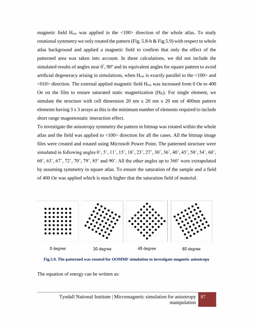
Tyndall National Institute | Micromagnetic simulation for anisotropy
manipulation
87
magnetic field Hext was applied in the <100> direction of the whole atlas. To study
rotational symmetry we only rotated the pattern (Fig. 5.8-b & Fig.5.9) with respect to whole
atlas background and applied a magnetic field to confirm that only the effect of the
patterned area was taken into account. In these calculations, we did not include the
simulated results of angles near 0º, 90º and its equivalent angles for square pattern to avoid
artificial degeneracy arising in simulations, when Hext is exactly parallel to the <100> and
<010> direction. The external applied magnetic field Hext was increased from 0 Oe to 400
Oe on the film to ensure saturated static magnetization (HK). For single element, we
simulate the structure with cell dimension 20 nm x 20 nm x 20 nm of 400nm pattern
elements having 3 x 3 arrays as this is the minimum number of elements required to include
short range magnetostatic interaction effect.
To investigate the anisotropy symmetry the pattern in bitmap was rotated within the whole
atlas and the field was applied to <100> direction for all the cases. All the bitmap image
files were created and rotated using Microsoft Power Point. The patterned structure were
simulated in following angles 0˚, 5˚, 11˚, 15˚, 18˚, 23˚, 27˚, 30˚, 36˚, 40˚, 45˚, 50˚, 54˚, 60˚,
60˚, 63˚, 67˚, 72˚, 70˚, 79˚, 85˚ and 90˚. All the other angles up to 360˚ were extrapolated
by assuming symmetry in square atlas. To ensure the saturation of the sample and a field
of 400 Oe was applied which is much higher that the saturation field of material.
Fig.5.9. The patterned was rotated for OOMMF simulation to investigate magnetic anisotropy
The equation of energy can be written as:
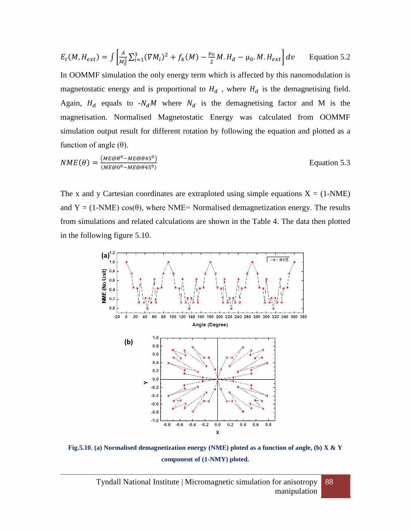
Tyndall National Institute | Micromagnetic simulation for anisotropy
manipulation
88
𝐸𝑡(𝑀, 𝐻𝑒𝑥𝑡) = ∫ [𝐴
𝑀𝑆2 ∑ (𝛻𝑀𝑖)
23𝑖=1 + 𝑓𝑘(𝑀) −
µ0
2𝑀. 𝐻𝑑 − µ0. 𝑀. 𝐻𝑒𝑥𝑡] 𝑑𝑣 Equation 5.2
In OOMMF simulation the only energy term which is affected by this nanomodulation is
magnetostatic energy and is proportional to 𝐻𝑑 , where 𝐻𝑑 is the demagnetising field.
Again, 𝐻𝑑 equals to -𝑁𝑑𝑀 where 𝑁𝑑 is the demagnetising factor and M is the
magnetisation. Normalised Magnetostatic Energy was calculated from OOMMF
simulation output result for different rotation by following the equation and plotted as a
function of angle (θ).
𝑁𝑀𝐸(𝜃) =(𝑀𝐸@𝜃0−𝑀𝐸@𝜃450)
(𝑀𝐸@00−𝑀𝐸@𝜃450) Equation 5.3
The x and y Cartesian coordinates are extraploted using simple equations X = (1-NME)
and Y = (1-NME) cos(θ), where NME= Normalised demagnetization energy. The results
from simulations and related calculations are shown in the Table 4. The data then plotted
in the following figure 5.10.
Fig.5.10. (a) Normalised demagnetization energy (NME) ploted as a function of angle, (b) X & Y
component of (1-NMY) ploted.
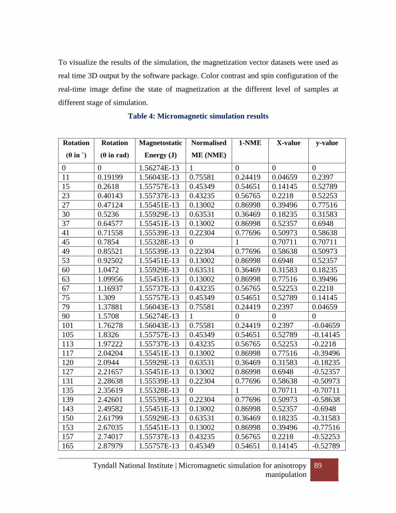
Tyndall National Institute | Micromagnetic simulation for anisotropy
manipulation
89
To visualize the results of the simulation, the magnetization vector datasets were used as
real time 3D output by the software package. Color contrast and spin configuration of the
real-time image define the state of magnetization at the different level of samples at
different stage of simulation.
Table 4: Micromagnetic simulation results
Rotation
(θ in ˚)
Rotation
(θ in rad)
Magnetostatic
Energy (J)
Normalised
ME (NME)
1-NME X-value y-value
0 0 1.56274E-13 1 0 0 0
11 0.19199 1.56043E-13 0.75581 0.24419 0.04659 0.2397
15 0.2618 1.55757E-13 0.45349 0.54651 0.14145 0.52789
23 0.40143 1.55737E-13 0.43235 0.56765 0.2218 0.52253
27 0.47124 1.55451E-13 0.13002 0.86998 0.39496 0.77516
30 0.5236 1.55929E-13 0.63531 0.36469 0.18235 0.31583
37 0.64577 1.55451E-13 0.13002 0.86998 0.52357 0.6948
41 0.71558 1.55539E-13 0.22304 0.77696 0.50973 0.58638
45 0.7854 1.55328E-13 0 1 0.70711 0.70711
49 0.85521 1.55539E-13 0.22304 0.77696 0.58638 0.50973
53 0.92502 1.55451E-13 0.13002 0.86998 0.6948 0.52357
60 1.0472 1.55929E-13 0.63531 0.36469 0.31583 0.18235
63 1.09956 1.55451E-13 0.13002 0.86998 0.77516 0.39496
67 1.16937 1.55737E-13 0.43235 0.56765 0.52253 0.2218
75 1.309 1.55757E-13 0.45349 0.54651 0.52789 0.14145
79 1.37881 1.56043E-13 0.75581 0.24419 0.2397 0.04659
90 1.5708 1.56274E-13 1 0 0 0
101 1.76278 1.56043E-13 0.75581 0.24419 0.2397 -0.04659
105 1.8326 1.55757E-13 0.45349 0.54651 0.52789 -0.14145
113 1.97222 1.55737E-13 0.43235 0.56765 0.52253 -0.2218
117 2.04204 1.55451E-13 0.13002 0.86998 0.77516 -0.39496
120 2.0944 1.55929E-13 0.63531 0.36469 0.31583 -0.18235
127 2.21657 1.55451E-13 0.13002 0.86998 0.6948 -0.52357
131 2.28638 1.55539E-13 0.22304 0.77696 0.58638 -0.50973
135 2.35619 1.55328E-13 0 1 0.70711 -0.70711
139 2.42601 1.55539E-13 0.22304 0.77696 0.50973 -0.58638
143 2.49582 1.55451E-13 0.13002 0.86998 0.52357 -0.6948
150 2.61799 1.55929E-13 0.63531 0.36469 0.18235 -0.31583
153 2.67035 1.55451E-13 0.13002 0.86998 0.39496 -0.77516
157 2.74017 1.55737E-13 0.43235 0.56765 0.2218 -0.52253
165 2.87979 1.55757E-13 0.45349 0.54651 0.14145 -0.52789
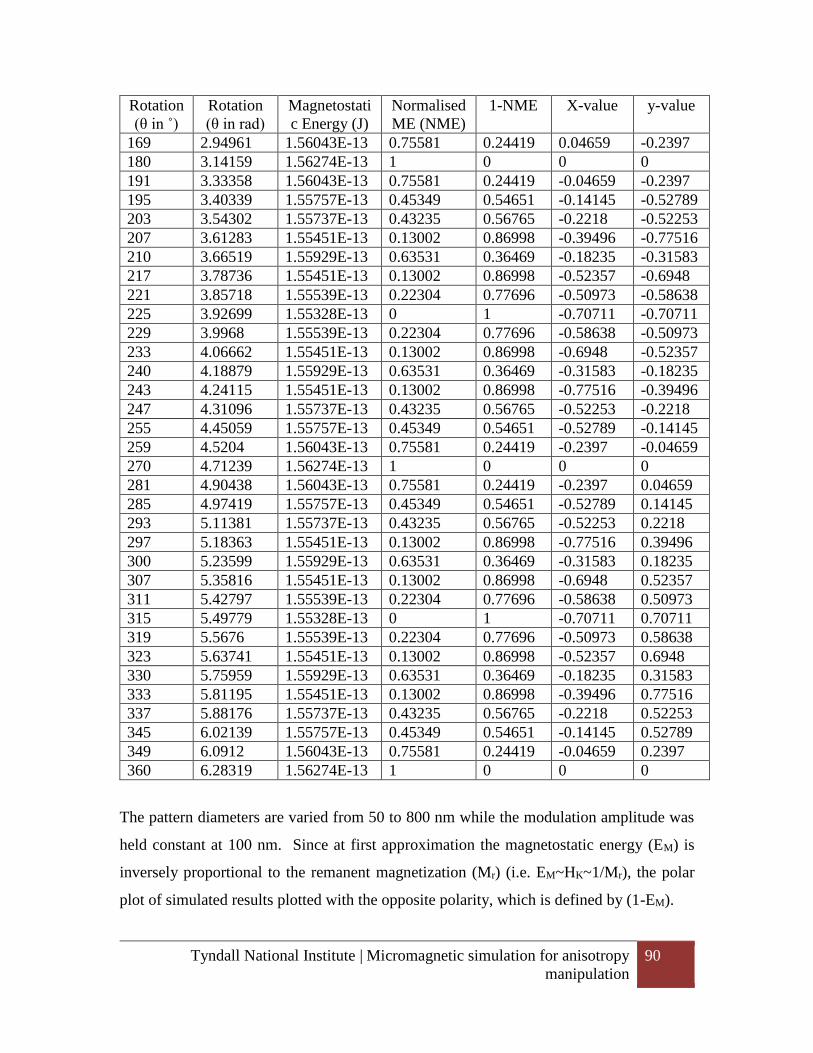
Tyndall National Institute | Micromagnetic simulation for anisotropy
manipulation
90
Rotation
(θ in ˚)
Rotation
(θ in rad)
Magnetostati
c Energy (J)
Normalised
ME (NME)
1-NME X-value y-value
169 2.94961 1.56043E-13 0.75581 0.24419 0.04659 -0.2397
180 3.14159 1.56274E-13 1 0 0 0
191 3.33358 1.56043E-13 0.75581 0.24419 -0.04659 -0.2397
195 3.40339 1.55757E-13 0.45349 0.54651 -0.14145 -0.52789
203 3.54302 1.55737E-13 0.43235 0.56765 -0.2218 -0.52253
207 3.61283 1.55451E-13 0.13002 0.86998 -0.39496 -0.77516
210 3.66519 1.55929E-13 0.63531 0.36469 -0.18235 -0.31583
217 3.78736 1.55451E-13 0.13002 0.86998 -0.52357 -0.6948
221 3.85718 1.55539E-13 0.22304 0.77696 -0.50973 -0.58638
225 3.92699 1.55328E-13 0 1 -0.70711 -0.70711
229 3.9968 1.55539E-13 0.22304 0.77696 -0.58638 -0.50973
233 4.06662 1.55451E-13 0.13002 0.86998 -0.6948 -0.52357
240 4.18879 1.55929E-13 0.63531 0.36469 -0.31583 -0.18235
243 4.24115 1.55451E-13 0.13002 0.86998 -0.77516 -0.39496
247 4.31096 1.55737E-13 0.43235 0.56765 -0.52253 -0.2218
255 4.45059 1.55757E-13 0.45349 0.54651 -0.52789 -0.14145
259 4.5204 1.56043E-13 0.75581 0.24419 -0.2397 -0.04659
270 4.71239 1.56274E-13 1 0 0 0
281 4.90438 1.56043E-13 0.75581 0.24419 -0.2397 0.04659
285 4.97419 1.55757E-13 0.45349 0.54651 -0.52789 0.14145
293 5.11381 1.55737E-13 0.43235 0.56765 -0.52253 0.2218
297 5.18363 1.55451E-13 0.13002 0.86998 -0.77516 0.39496
300 5.23599 1.55929E-13 0.63531 0.36469 -0.31583 0.18235
307 5.35816 1.55451E-13 0.13002 0.86998 -0.6948 0.52357
311 5.42797 1.55539E-13 0.22304 0.77696 -0.58638 0.50973
315 5.49779 1.55328E-13 0 1 -0.70711 0.70711
319 5.5676 1.55539E-13 0.22304 0.77696 -0.50973 0.58638
323 5.63741 1.55451E-13 0.13002 0.86998 -0.52357 0.6948
330 5.75959 1.55929E-13 0.63531 0.36469 -0.18235 0.31583
333 5.81195 1.55451E-13 0.13002 0.86998 -0.39496 0.77516
337 5.88176 1.55737E-13 0.43235 0.56765 -0.2218 0.52253
345 6.02139 1.55757E-13 0.45349 0.54651 -0.14145 0.52789
349 6.0912 1.56043E-13 0.75581 0.24419 -0.04659 0.2397
360 6.28319 1.56274E-13 1 0 0 0
The pattern diameters are varied from 50 to 800 nm while the modulation amplitude was
held constant at 100 nm. Since at first approximation the magnetostatic energy (EM) is
inversely proportional to the remanent magnetization (Mr) (i.e. EM~HK~1/Mr), the polar
plot of simulated results plotted with the opposite polarity, which is defined by (1-EM).
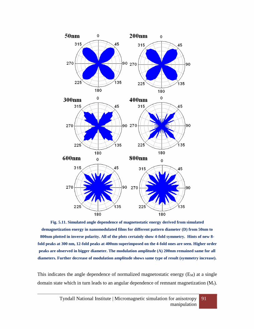
Tyndall National Institute | Micromagnetic simulation for anisotropy
manipulation
91
Fig. 5.11. Simulated angle dependence of magnetostatic energy derived from simulated
demagnetization energy in nanomodulated films for different pattern diameter (D) from 50nm to
800nm plotted in inverse polarity. All of the plots certainly show 4-fold symmetry. Hints of new 8-
fold peaks at 300 nm, 12-fold peaks at 400nm superimposed on the 4-fold ones are seen. Higher order
peaks are observed in bigger diameter. The modulation amplitude (A) 200nm remained same for all
diameters. Further decrease of modulation amplitude shows same type of result (symmetry increase).
This indicates the angle dependence of normalized magnetostatic energy (EM) at a single
domain state which in turn leads to an angular dependence of remnant magnetization (Mr).
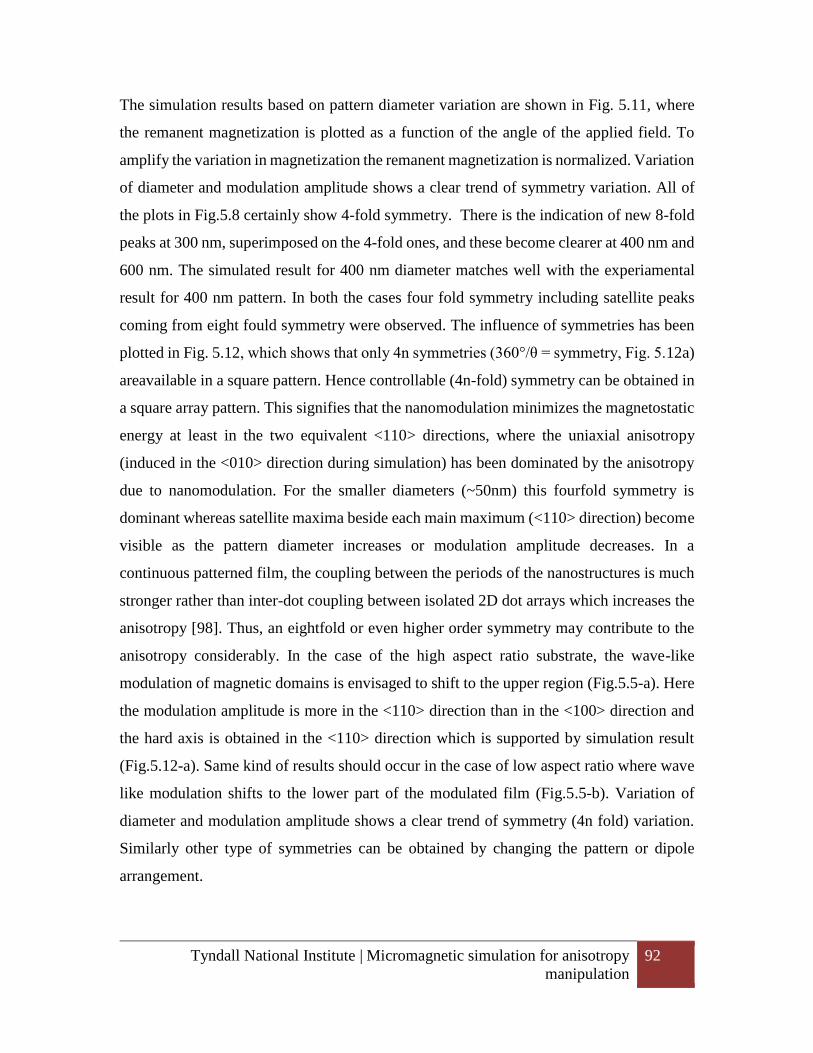
Tyndall National Institute | Micromagnetic simulation for anisotropy
manipulation
92
The simulation results based on pattern diameter variation are shown in Fig. 5.11, where
the remanent magnetization is plotted as a function of the angle of the applied field. To
amplify the variation in magnetization the remanent magnetization is normalized. Variation
of diameter and modulation amplitude shows a clear trend of symmetry variation. All of
the plots in Fig.5.8 certainly show 4-fold symmetry. There is the indication of new 8-fold
peaks at 300 nm, superimposed on the 4-fold ones, and these become clearer at 400 nm and
600 nm. The simulated result for 400 nm diameter matches well with the experiamental
result for 400 nm pattern. In both the cases four fold symmetry including satellite peaks
coming from eight fould symmetry were observed. The influence of symmetries has been
plotted in Fig. 5.12, which shows that only 4n symmetries (360°/θ = symmetry, Fig. 5.12a)
areavailable in a square pattern. Hence controllable (4n-fold) symmetry can be obtained in
a square array pattern. This signifies that the nanomodulation minimizes the magnetostatic
energy at least in the two equivalent <110> directions, where the uniaxial anisotropy
(induced in the <010> direction during simulation) has been dominated by the anisotropy
due to nanomodulation. For the smaller diameters (~50nm) this fourfold symmetry is
dominant whereas satellite maxima beside each main maximum (<110> direction) become
visible as the pattern diameter increases or modulation amplitude decreases. In a
continuous patterned film, the coupling between the periods of the nanostructures is much
stronger rather than inter-dot coupling between isolated 2D dot arrays which increases the
anisotropy [98]. Thus, an eightfold or even higher order symmetry may contribute to the
anisotropy considerably. In the case of the high aspect ratio substrate, the wave-like
modulation of magnetic domains is envisaged to shift to the upper region (Fig.5.5-a). Here
the modulation amplitude is more in the <110> direction than in the <100> direction and
the hard axis is obtained in the <110> direction which is supported by simulation result
(Fig.5.12-a). Same kind of results should occur in the case of low aspect ratio where wave
like modulation shifts to the lower part of the modulated film (Fig.5.5-b). Variation of
diameter and modulation amplitude shows a clear trend of symmetry (4n fold) variation.
Similarly other type of symmetries can be obtained by changing the pattern or dipole
arrangement.
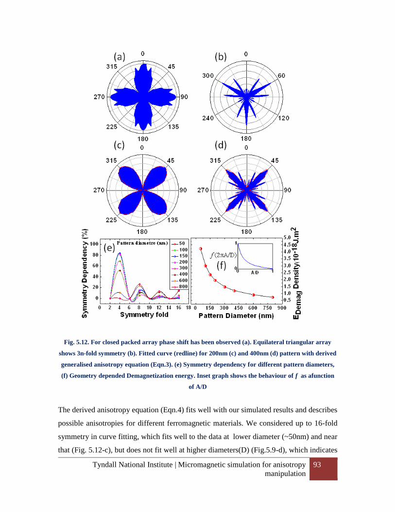
Tyndall National Institute | Micromagnetic simulation for anisotropy
manipulation
93
Fig. 5.12. For closed packed array phase shift has been observed (a). Equilateral triangular array
shows 3n-fold symmetry (b). Fitted curve (redline) for 200nm (c) and 400nm (d) pattern with derived
generalised anisotropy equation (Eqn.3). (e) Symmetry dependency for different pattern diameters,
(f) Geometry depended Demagnetization energy. Inset graph shows the behaviour of f as afunction
of A/D
The derived anisotropy equation (Eqn.4) fits well with our simulated results and describes
possible anisotropies for different ferromagnetic materials. We considered up to 16-fold
symmetry in curve fitting, which fits well to the data at lower diameter (~50nm) and near
that (Fig. 5.12-c), but does not fit well at higher diameters(D) (Fig.5.9-d), which indicates
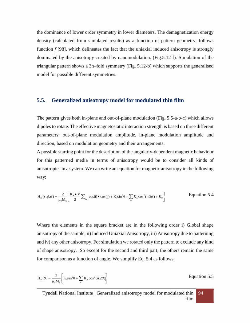
Tyndall National Institute | Generalized anisotropy model for modulated thin
film
94
the dominance of lower order symmetry in lower diameters. The demagnetization energy
density (calculated from simulated results) as a function of pattern geometry, follows
function f [98], which delineates the fact that the uniaxial induced anisotropy is strongly
dominated by the anisotropy created by nanomodulation. (Fig.5.12-f). Simulation of the
triangular pattern shows a 3n–fold symmetry (Fig. 5.12-b) which supports the generalised
model for possible different symmetries.
5.5. Generalized anisotropy model for modulated thin film
The pattern gives both in-plane and out-of-plane modulation (Fig. 5.5-a-b-c) which allows
dipoles to rotate. The effective magnetostatic interaction strength is based on three different
parameters: out-of-plane modulation amplitude, in-plane modulation amplitude and
direction, based on modulation geometry and their arrangements.
A possible starting point for the description of the angularly-dependent magnetic behaviour
for this patterned media in terms of anisotropy would be to consider all kinds of
anisotropies in a system. We can write an equation for magnetic anisotropy in the following
way:
0
22
Iji
S
S0
K )2.(cosθsinKj)cos(i)cos(2
VK
Mμ
2),,(H KnKr
n
n Equation 5.4
Where the elements in the square bracket are in the following order i) Global shape
anisotropy of the sample, ii) Induced Uniaxial Anisotropy, iii) Anisotropy due to patterning
and iv) any other anisotropy. For simulation we rotated only the pattern to exclude any kind
of shape anisotropy. So except for the second and third part, the others remain the same
for comparison as a function of angle. We simplify Eq. 5.4 as follows.
n
n nK )2.(cosθsinKMμ
2)(H 22
I
S0
K Equation 5.5
Tyndall National Institute | Generalized anisotropy model for modulated thin
film
95
We generalise a possible directional symmetry where n = β/α; α is a number representing
a minimum geometrical symmetry (i.e. 4 for square, 3 for equilateral triangular/hexagon)
and β is a positive integer. Kn denotes the anisotropy constant for the corresponding
symmetries. In nanomodulated films the magnetization follows a wave-like path due to
modulation geometry [98] and creates two types of magnetic charge dipoles. Since
magnetic induction B=μ0 (H+M) don’t have divergence, the points where lines of
magnetization originate or terminate can be considered as magnetic charge poles with
opposite polarity. Looking through the cross section the magnetization directions are
opposite to each other at two sides of an element which creates an out-of-plane dipoles
(Fig. 5.5-a-b). In the case of in-plane view magnetization directions at reverse sides of an
element are of opposite polarity in an external magnetic field direction, which gives in-
plane dipoles (Fig. 5-c). These dipoles can interact with each other strongly only when
there is a chain of elements in the applied field directions, creating an anisotropic
magnetization throughout whole film. We consider all types of magnetic interaction in
different region and by using sum rules given by Yafet, et. Al [99] the total magnetostatic
energy is given by,
VAM S
2z
mag
y
mag
x
magmag 42
1EEEE
Equation 5.6
where
MS is the saturation magnetization,
V is the volume
and A is modulation amplitude.
Since by symmetry in a square struture;
mag
y
mag
x
mag EEE Equation 5.7
magnetostatic energy becomes,
VAπMEEE Smagmagmag
24
2
12
. Equation 5.8
Tyndall National Institute | Generalized anisotropy model for modulated thin
film
96
For an externally applied field H the magnetostatic energy can be written as
dvH.M2
1Emag
. We can consider two different layers of the pattern with magnetic
and nonmagnetic regions in each layer. The magnetization can be written as
L
2
L
1
U
2
U
1 MMMMM for an applied field L
2
L
1
U
2
U
1 HHHHH (U ~ Upper
layer, L ~ Lower Layer, 1 is magnetic region and 2 is nonmagnetic region) for 4 different
cases. Then we can write magnetostatic energy in following way for patterned structure,
vdH.M2
1E mn,
j
mn,i
mn,
mag
Equation 5.9
Where the distribution of magnetization can be expanded in Fourier series as follows,
And the field correspond to each magnetization will be, j
i
j
i πdivMdivH 4
The inter-layer interaction gives perpendicular anisotropy and the remaining effects give
in-plane anisotropy. M. Rewienski [101] found magnetic anisotropy of ferromagnetic thin-
films due to surface roughness. Using the same principle we have calculated the anisotropy
energy due to each single element as
D
Af(2π1A
4
1M
2
1CE
2
Simag
and
D
Af(2π1A
2
1M
2
1CE
2
Simag where Ci is a constant which
depends on pattern geometry and aspect ratio. The function [101] f is 0 at A/D=1 and 1 at
A/D=0 (Fig. 5-f inset). The dipolar anisotropy is given by 0EEE mag
||
magda which
gives a finite dipolar anisotropy energy depending upon the modulation geometry.
Considering up to second-order harmonics, we can rewrite the dipolar anisotropy for
anisotropy energy as
D
AfAM.CK Si
S21
4
34
2
1 2 , where A is the amplitude of
modulation and D is the diameter of the element. The magnetostatic interaction strength
depends on the density of elements in a particular direction. So we add another term sin
(90°/β) for patterned induced magnetic anisotropy where β is a positive integer.
Using the expression for KS we can then rewrite Eq. 5.2
.α
2θβcos
β
90sin
D
A2πf1A.C
Mμ
2)(H 2
nS0
K
Equation 5.10

Tyndall National Institute | Generalized anisotropy model for modulated thin
film
97
Where, n = β/α, α is a number representing a minimum geometrical symmetry (i.e., four
for square, three for equilateral triangular/hexagonal), the constant C depends upon single
element geometry and diameter/separation (D/S). This equation describes the possibility of
anisotropy variation by nanomodulation geometry for different ferromagnetic materials.
The magnetostatic energy due to the dipolar configuration can be expressed as follows. For
this model we assumed that each pattern has a single domain magnetic dipole, circularly
shaped, they can be rotated across the center of dipole moment and the
Equation 5.11
neighboring spins are not exchanged coupled. The system energy includes magnetostatic
energy and the Zeeman energy while exchange coupling is neglected.
xternaldipoleTotal E EE Equation 5.12
And
Where g is the gyromagnetic factor and μB is the Bohr magneton.
The total dipolar energy in the infinite array can be expressed as
ii R ij
ijjiji
ij
ji
R
BR
)R.M)(R.M(
R
M.Mg
53
22
dipole 32
1E
Equation 5.13
i
iextternalextternal M.HE Equation 5.14
Where g is the gyromagnetic factor and μB is the Bohr magneton.
The total magnetostatic energy is the sum of surface and volume energy generated due the
in plane and out of plane dipole formation and inter dipole interaction at the volume and
surface of nanomodulated thin film.
surfacevolumeTotal E EE Equation 5.15
The total dipolar energy in the infinite array can be expressed as
dSR
R)R(mM.ndV
R
R)R(mM.E
ij
ij
SurfaceeSample
iiSs
ij
ij
VolumeSample
iiSTotal 33
Equation 5.16
y)x)sin(ksin(kMy)M(x, mn
0m
j
mn,i
0n
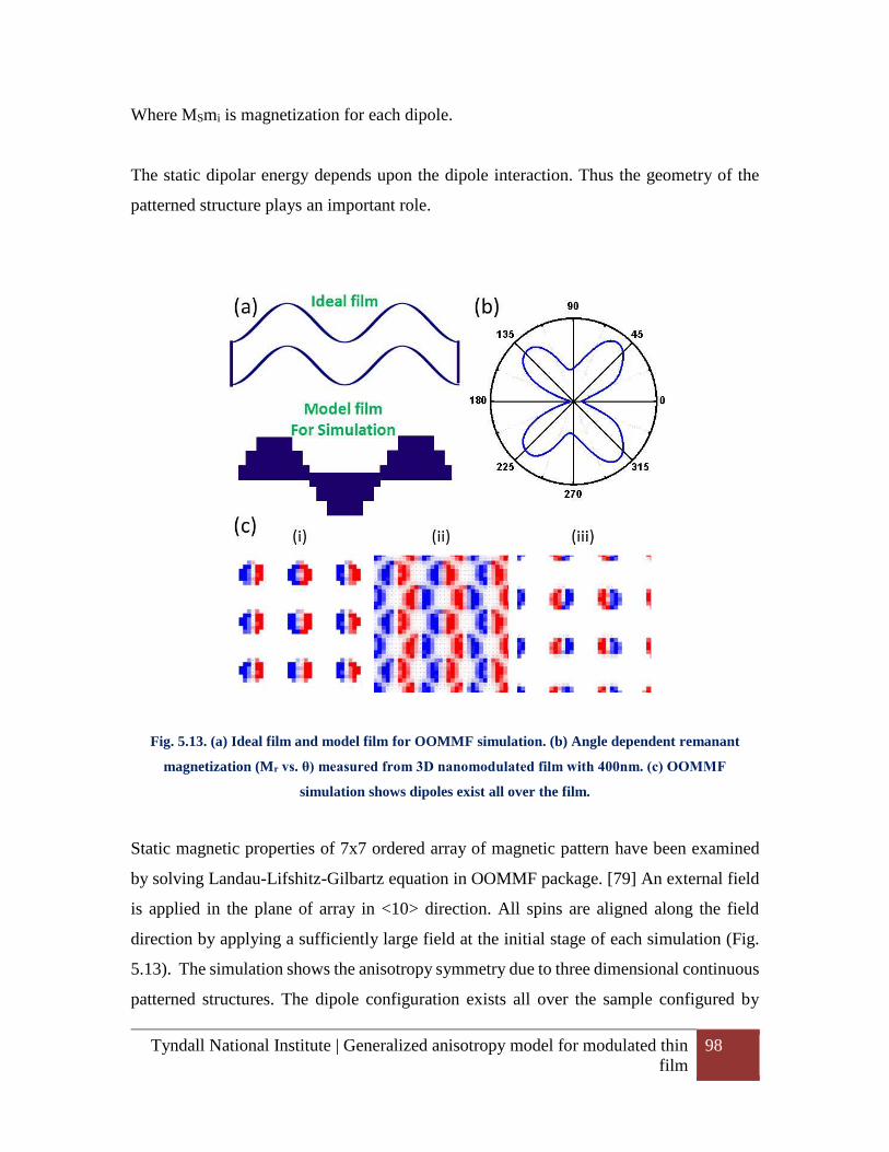
Tyndall National Institute | Generalized anisotropy model for modulated thin
film
98
Where MSmi is magnetization for each dipole.
The static dipolar energy depends upon the dipole interaction. Thus the geometry of the
patterned structure plays an important role.
Fig. 5.13. (a) Ideal film and model film for OOMMF simulation. (b) Angle dependent remanant
magnetization (Mr vs. θ) measured from 3D nanomodulated film with 400nm. (c) OOMMF
simulation shows dipoles exist all over the film.
Static magnetic properties of 7x7 ordered array of magnetic pattern have been examined
by solving Landau-Lifshitz-Gilbartz equation in OOMMF package. [79] An external field
is applied in the plane of array in <10> direction. All spins are aligned along the field
direction by applying a sufficiently large field at the initial stage of each simulation (Fig.
5.13). The simulation shows the anisotropy symmetry due to three dimensional continuous
patterned structures. The dipole configuration exists all over the sample configured by
Tyndall National Institute | Summary 99
pattern geometry (Fig. 5.13.c). The rotation of the field rotates the magnetic dipole. The
strength of dipolar energy varies depending upon array symmetry and magnetostatic energy
varies accordingly.
5.6. Summary
In this chapter, the variation of magnetic anisotropy is investigated through the formation
of magnetic dipoles in continuous ferromagnetic thin-films due to a unique
nanomodulation. Experimental evidence of well-ordered dipoles with metastable state have
been detected by means of variation of magnetic anisotropy, step hysteresis and MFM
imaging. The novel 3D modulation generates both in plane and out of plane dipoles, where
the competition between in-plane and out of plane dipoles creates metastable state giving
opportunity to manipulate anisotropy. The anisotropy model, based on collective dipolar
interaction was used to demonstrate the ability to control anisotropy in continuous
ferromagnetic thin-films by minimizing magnetostatic energy through nanomodulation.
The change of diameter/separation ratio (D/S) in nanomodulation can switch the anisotropy
direction due to the transformation of the modulation wave from one layer to another layer.
The generalised model helps us to find out possible anisotropy based on material property
and geometrical arrangement of nanopattern. By varying amplitude/diameter (A/D) ratio
and geometrical arrangement (α) one can achieve desired anisotropy. Thicknesses close to
the modulation amplitude provide more control over the anisotropy. Additionally, the
formation of a metastable single domain resists vortex formation in nanopatterned
ferromagnetic thin-films which is essential for realizing devices such as volatile memory,
magnetically frustrated patterned media [90], highly integrated nanoscale magnetic devices
[101, 102] etc. Fourier analysis of magnetostatic energy for this nanomodulated film
supports the existence of magnetic diploes (Eda≠0). The derived generalised mathematical
expression based on magnetic dipolar interaction is found to be in good agreement with
our results, which can help to estimate and understand the anisotropy in other pattern media
also. The method described in this work is much simpler and can be demonstrated at a
larger scale.In this unique three dimensional continuous ferromagnetic film the
magnetostatic energy is tuned by magnetic interaction among the magnetic dipoles in

Tyndall National Institute | 100
patterned array with in-plane external magnetic field. A strong out of plane dipoles are
generated by in-plane magnetic field and the competition between in-plane and out-of-
plane magnetic dipole resists vortex formation in nanostructure thin ferromagnetic film
which can be a key factor in high density storage media. The micromagnetic simulation
shows a qualitative agreement with the experimental results.
Tyndall National Institute | Chapter – Giant exchange anisotropy in Bismuth
ferrite (BFO) nanocomposite
101
6 Chapter – Giant exchange anisotropy in Bismuth ferrite (BFO)
nanocomposite
6.1. Introduction
In a period spanning more than five decades now, exchange anisotropyor exchange bias
effect has been observed in a multitude of magnetic heterostructures: (i) ferromagnet-
antiferromagnet [18], (ii) ferromagnet-spin glass [104], (iii) ferrimagnet-antiferromagnet
[105], (iv) ferrimagnet-ferromagnet [106], (v) ferromagnet spin glass-antiferromagnet
[107], etc. Conventionally, the exchange bias—measured by the shift of the magnetic
hysteresis loop along the field axis—requires pre-biasing of the interface moment via a
field cooling protocol from above the magnetic transition point [108]. This pre-biasing sets
the unidirectional anisotropy by breaking the symmetry of the interface moment. Exchange
bias has also been observed, spontaneously, when even in the absence of pre-biasing,
unidirectional anisotropy sets in under the first field of loop evaluation [109, 110], where
the sample is cooled down from above the transition point under zero field. The
spontaneous exchange bias (SEB), where the unidirectional anisotropy (UA) sets in
spontaneously under the application of the first field of a hysteresis loop even in an
unmagnetized state, is a consequence, primarily, of biaxial symmetry in the
antiferromagnetic (AFM) structure of ferromagnetic (FM)-AFM interface [111-113]. In a
spin glass (SG)-FM structure, on the other hand, the anisotropy sets in under field cooling
via oscillatory Ruderman-Kittel-Kasuya-Yosida (RKKY) interaction [114]. However, we
demonstrate in this chapter that glassy moments at the interface, in fact, introduce an
additional magnetic degree of freedom in between the exchange coupled FM and AFM
grains and breaks the symmetry truly spontaneously even before the application of the first
field of a loop to set the UA in an unmagnetized state. As discussed later, the consequence
of this is an asymmetry in the SEB depending on the path followed in tracing the hysteresis
loop—positive or negative. In a nanocomposite of BiFeO3 (~94%)-Bi2Fe4O9 (~6%),we
observed (i) a large SEB (~300–600 Oe) across 5–300 K, (ii) asymmetry in SEB depending
on the path followed in tracing the hysteresis loop—positive or negative, and (iii) a
Tyndall National Institute | BiFeO3-Bi2Fe4O9 nano-composite 102
nonmonotonic variation of SEB with temperature. The magnitude of the SEB itself is far
higher than what has so far been observed in all the bulk or thin film based composites of
BiFeO3 [115–118] even under magnetic annealing. We have also observed the
conventional magnetic-annealing-dependent exchange bias (CEB) with all its regular
features such as dependence on annealing field, rate, and training. The random field
generated by the glassy moments at the shell appears to be influencing the indirect
exchange bias coupling called ‘‘superinteraction bias coupling’’ between the FM core
[120] of finer Bi2Fe4O9 and local moments of AFM order in coarser BiFeO3and inducing
the SEB, its path dependence, and its nonmonotonicity in variation with temperature. This
has been investigated in nanocomposite of ~112 nm BiFeO3 and ~19 nm Bi2Fe4O9.
6.2. BiFeO3-Bi2Fe4O9 nano-composite
6.2.1. Sample preparation
The nanocomposite of BiFeO3-Bi2Fe4O9 has been synthesized at Central Glass and
Ceramic Research Institute (CGCRI) - India by sonochemical route where coprecipitation
from aqueous solution of mixed metal nitrates takes place in presence of ultrasonic
vibration. The precipitate thus formed is collected in a centrifuge running at 12000 rpm.
The powder is finally washed, dried and calcined at 350-550oC for 4-5h in air. The pH of
the medium of coprecipitation, ultrasonic vibration energy, heat-treatment temperature,
and time etc. can be controlled to yield nano-sized particles of either pure BiFeO3 or a
nanocomposite of BiFeO3-Bi2Fe4O9 of varying concentration ratio of the component
phases. Three type of nanocomposite was prepared: BFO-A with 112 nm BiFeO3 (~94%)-
19 nm Bi2Fe4O9 (~6%),BFO-B 57 nm BiFeO3 (~90%)- 13 nm Bi2Fe4O9 (~10%) and BFO-
C (pure BiFeO3).
6.2.2. Structural analysis
The particle morphology and the crystallographic details have been studied by transmission
electron microscopy (TEM), selected area electron diffraction (SAED), and high resolution
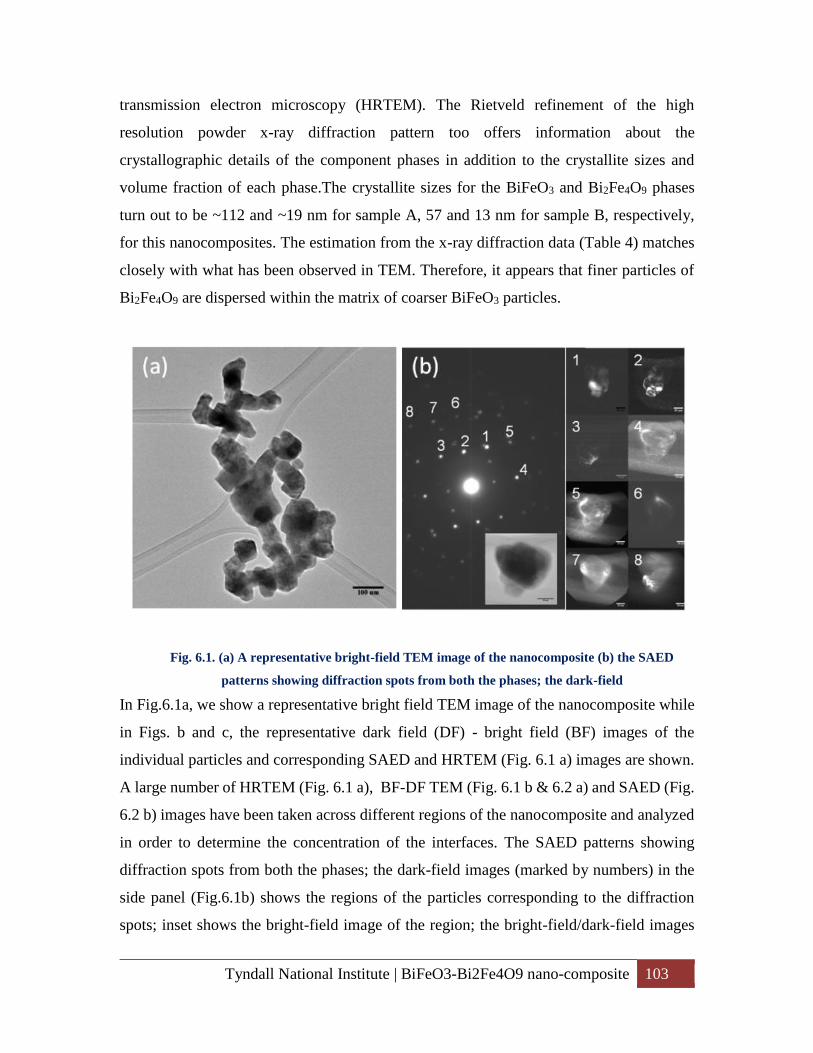
Tyndall National Institute | BiFeO3-Bi2Fe4O9 nano-composite 103
transmission electron microscopy (HRTEM). The Rietveld refinement of the high
resolution powder x-ray diffraction pattern too offers information about the
crystallographic details of the component phases in addition to the crystallite sizes and
volume fraction of each phase.The crystallite sizes for the BiFeO3 and Bi2Fe4O9 phases
turn out to be ~112 and ~19 nm for sample A, 57 and 13 nm for sample B, respectively,
for this nanocomposites. The estimation from the x-ray diffraction data (Table 4) matches
closely with what has been observed in TEM. Therefore, it appears that finer particles of
Bi2Fe4O9 are dispersed within the matrix of coarser BiFeO3 particles.
Fig. 6.1. (a) A representative bright-field TEM image of the nanocomposite (b) the SAED
patterns showing diffraction spots from both the phases; the dark-field
In Fig.6.1a, we show a representative bright field TEM image of the nanocomposite while
in Figs. b and c, the representative dark field (DF) - bright field (BF) images of the
individual particles and corresponding SAED and HRTEM (Fig. 6.1 a) images are shown.
A large number of HRTEM (Fig. 6.1 a), BF-DF TEM (Fig. 6.1 b & 6.2 a) and SAED (Fig.
6.2 b) images have been taken across different regions of the nanocomposite and analyzed
in order to determine the concentration of the interfaces. The SAED patterns showing
diffraction spots from both the phases; the dark-field images (marked by numbers) in the
side panel (Fig.6.1b) shows the regions of the particles corresponding to the diffraction
spots; inset shows the bright-field image of the region; the bright-field/dark-field images
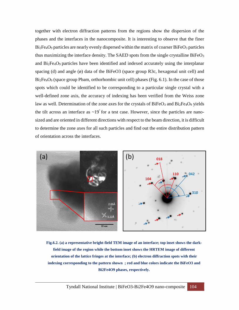
Tyndall National Institute | BiFeO3-Bi2Fe4O9 nano-composite 104
together with electron diffraction patterns from the regions show the dispersion of the
phases and the interfaces in the nanocomposite. It is interesting to observe that the finer
Bi2Fe4O9 particles are nearly evenly dispersed within the matrix of coarser BiFeO3 particles
thus maximizing the interface density. The SAED spots from the single crystalline BiFeO3
and Bi2Fe4O9 particles have been identified and indexed accurately using the interplanar
spacing (d) and angle (ø) data of the BiFeO3 (space group R3c, hexagonal unit cell) and
Bi2Fe4O9 (space group Pbam, orthorhombic unit cell) phases (Fig. 6.1). In the case of those
spots which could be identified to be corresponding to a particular single crystal with a
well-defined zone axis, the accuracy of indexing has been verified from the Weiss zone
law as well. Determination of the zone axes for the crystals of BiFeO3 and Bi2Fe4O9 yields
the tilt across an interface as ~19º for a test case. However, since the particles are nano-
sized and are oriented in different directions with respect to the beam direction, it is difficult
to determine the zone axes for all such particles and find out the entire distribution pattern
of orientation across the interfaces.
Fig.6.2. (a) a representative bright-field TEM image of an interface; top inset shows the dark-
field image of the region while the bottom inset shows the HRTEM image of different
orientation of the lattice fringes at the interface; (b) electron diffraction spots with their
indexing corresponding to the pattern shown ; red and blue colors indicate the BiFeO3 and
Bi2Fe4O9 phases, respectively.
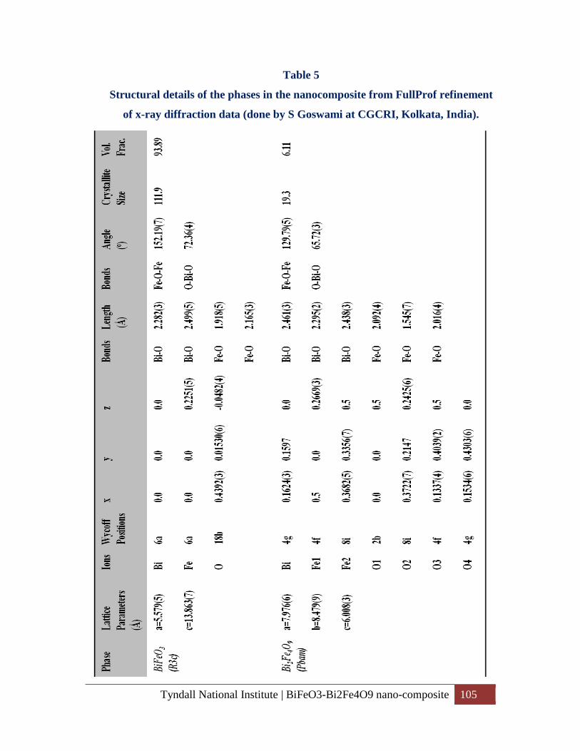
Tyndall National Institute | BiFeO3-Bi2Fe4O9 nano-composite 105
Table 5
Structural details of the phases in the nanocomposite from FullProf refinement
of x-ray diffraction data (done by S Goswami at CGCRI, Kolkata, India).
Tyndall National Institute | Magnetic measurements of exchange
anisotropy/exchange bias
106
6.3. Magnetic measurements of exchange anisotropy/exchange bias
The magnetic measurements have been carried out in a SQUID magnetometer (MPMS,
Quantum Design) across5-300 K under a maximum field Hm of 50 kOe. In order to ensure
that there is no trapped flux both in the superconducting coil of MPMS and in the sample
we followeda well-designed protocol to demagnetize them. An oscillating field with
varying amplitude, where the amplitude reduces from maximum to zero has typically been
applied. For example, for a demagnetizing field 1000Oe, the amplitude is brought down to
zero in the following sequence: (+1000) - (-900) - (+800) - (-700) ... (+50) - (-40) ... (+5) -
(-4) - (+3) - (-2) - (+1) - (0). The superconducting coils of MPMS are normally discharged
from high field (50 kOe) in oscillation mode; the amount of trapped flux is typically ~10
Oe. Before starting a new batch of experiments, the superconducting coil was warmed to
room temperature which is above the critical point. In addition, prior to the measurement
of SEB, the sample itself was demagnetized with oscillating field using an appropriate
protocol in order to ensure that there is no trapped flux in the sample.We have also
measured the SEB at 300 K for a maximum field of 18 kOe following zero-field cooling
(ZFC) from a high temperature (~700 K) - which is even above the magnetic transition
point TN (~590 K) of the AFM component - in a vibrating sample magnetometer for a test
case. We obtain an SEB of ~81 Oe at 300 K which is consistent with the SEB for different
Hm across 10-50 kOe measured in SQUID. This shows that the demagnetization protocol
used in SQUID was appropriate in ensuring unmagnetized state of the sample prior to the
measurement. We report here mainly the results obtained in a nanocomposite of ~6%
Bi2Fe4O9 and ~94% BiFeO3 (sample-A) which exhibits maximum SEB and CEB. In Fig.
6.3, the results from the magnetic measurements are shown. In Fig. 6.3 a, we show the
hysteresis loops which yield the SEB at several temperatures across 5-300 K. The region
near the origin is blown up to show the extent of EB clearly. We used a field step size of
100 Oe near the origin of hysteresis loop in order to measure the exchange bias accurately.
The field span of 10 kOe under such a protocol is covered typically within ~3h (~104s)
which gives the time scale of each of the measurements. In each case, the presence of a
large shift in the loop along the field axis is conspicuous. This shift cannot result from
relaxation of coercivity of the FM component as the tensorial nature of the
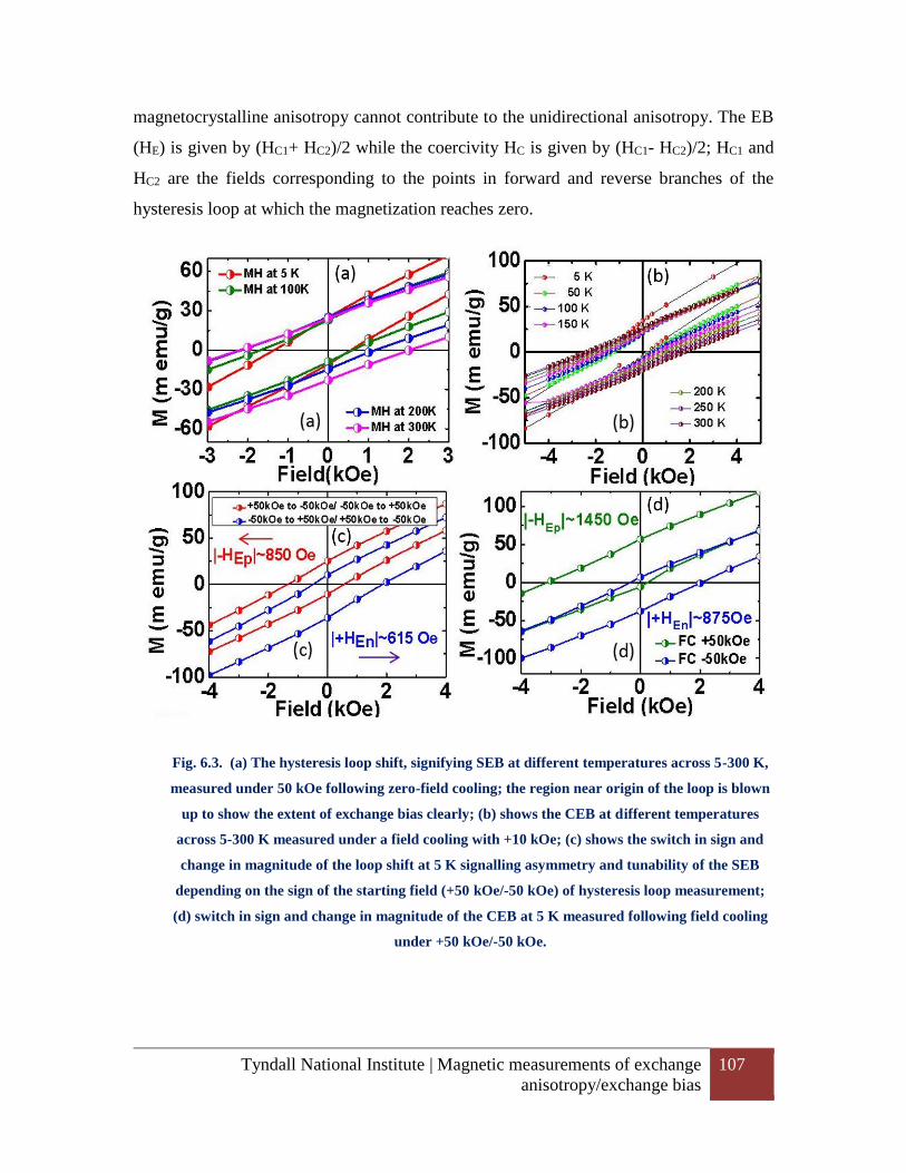
Tyndall National Institute | Magnetic measurements of exchange
anisotropy/exchange bias
107
magnetocrystalline anisotropy cannot contribute to the unidirectional anisotropy. The EB
(HE) is given by (HC1+ HC2)/2 while the coercivity HC is given by (HC1- HC2)/2; HC1 and
HC2 are the fields corresponding to the points in forward and reverse branches of the
hysteresis loop at which the magnetization reaches zero.
Fig. 6.3. (a) The hysteresis loop shift, signifying SEB at different temperatures across 5-300 K,
measured under 50 kOe following zero-field cooling; the region near origin of the loop is blown
up to show the extent of exchange bias clearly; (b) shows the CEB at different temperatures
across 5-300 K measured under a field cooling with +10 kOe; (c) shows the switch in sign and
change in magnitude of the loop shift at 5 K signalling asymmetry and tunability of the SEB
depending on the sign of the starting field (+50 kOe/-50 kOe) of hysteresis loop measurement;
(d) switch in sign and change in magnitude of the CEB at 5 K measured following field cooling
under +50 kOe/-50 kOe.
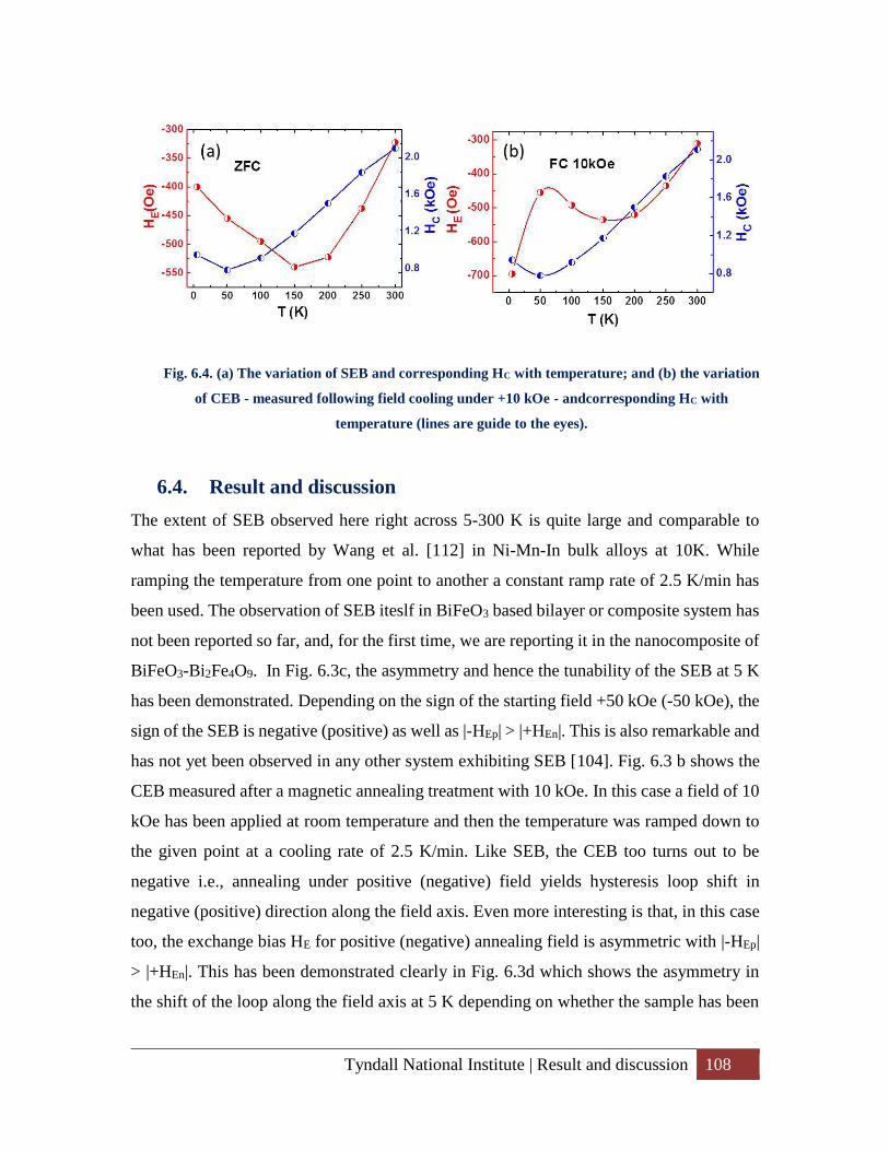
Tyndall National Institute | Result and discussion 108
Fig. 6.4. (a) The variation of SEB and corresponding HC with temperature; and (b) the variation
of CEB - measured following field cooling under +10 kOe - andcorresponding HC with
temperature (lines are guide to the eyes).
6.4. Result and discussion
The extent of SEB observed here right across 5-300 K is quite large and comparable to
what has been reported by Wang et al. [112] in Ni-Mn-In bulk alloys at 10K. While
ramping the temperature from one point to another a constant ramp rate of 2.5 K/min has
been used. The observation of SEB iteslf in BiFeO3 based bilayer or composite system has
not been reported so far, and, for the first time, we are reporting it in the nanocomposite of
BiFeO3-Bi2Fe4O9. In Fig. 6.3c, the asymmetry and hence the tunability of the SEB at 5 K
has been demonstrated. Depending on the sign of the starting field +50 kOe (-50 kOe), the
sign of the SEB is negative (positive) as well as |-HEp| > |+HEn|. This is also remarkable and
has not yet been observed in any other system exhibiting SEB [104]. Fig. 6.3 b shows the
CEB measured after a magnetic annealing treatment with 10 kOe. In this case a field of 10
kOe has been applied at room temperature and then the temperature was ramped down to
the given point at a cooling rate of 2.5 K/min. Like SEB, the CEB too turns out to be
negative i.e., annealing under positive (negative) field yields hysteresis loop shift in
negative (positive) direction along the field axis. Even more interesting is that, in this case
too, the exchange bias HE for positive (negative) annealing field is asymmetric with |-HEp|
> |+HEn|. This has been demonstrated clearly in Fig. 6.3d which shows the asymmetry in
the shift of the loop along the field axis at 5 K depending on whether the sample has been
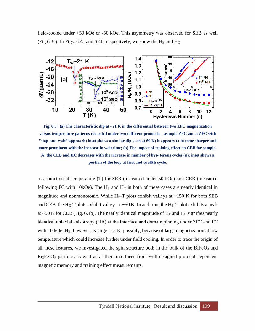
Tyndall National Institute | Result and discussion 109
field-cooled under +50 kOe or -50 kOe. This asymmetry was observed for SEB as well
(Fig.6.3c). In Figs. 6.4a and 6.4b, respectively, we show the HE and HC
Fig. 6.5. (a) The characteristic dip at ~21 K in the differential between two ZFC magnetization
versus temperature patterns recorded under two different protocols - asimple ZFC and a ZFC with
”stop-and-wait” approach; inset shows a similar dip even at 50 K; it appears to become sharper and
more prominent with the increase in wait time; (b) The impact of training effect on CEB for sample-
A; the CEB and HC decreases with the increase in number of hys- teresis cycles (n); inset shows a
portion of the loop at first and twelfth cycle.
as a function of temperature (T) for SEB (measured under 50 kOe) and CEB (measured
following FC with 10kOe). The HE and HC in both of these cases are nearly identical in
magnitude and nonmonotonic. While HE-T plots exhibit valleys at ~150 K for both SEB
and CEB, the HC-T plots exhibit valleys at ~50 K. In addition, the HE-T plot exhibits a peak
at ~50 K for CEB (Fig. 6.4b). The nearly identical magnitude of HE and HC signifies nearly
identical uniaxial anisotropy (UA) at the interface and domain pinning under ZFC and FC
with 10 kOe. HE, however, is large at 5 K, possibly, because of large magnetization at low
temperature which could increase further under field cooling. In order to trace the origin of
all these features, we investigated the spin structure both in the bulk of the BiFeO3 and
Bi2Fe4O9 particles as well as at their interfaces from well-designed protocol dependent
magnetic memory and training effect measurements.
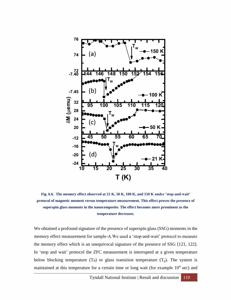
Tyndall National Institute | Result and discussion 110
Fig. 6.6. The memory effect observed at 21 K, 50 K, 100 K, and 150 K under ’stop-and-wait’
protocol of magnetic moment versus temperature measurement. This effect proves the presence of
superspin glass moments in the nanocomposite. The effect becomes more prominent as the
temperature decreases.
We obtained a profound signature of the presence of superspin glass (SSG) moments in the
memory effect measurement for sample-A.We used a ‘stop-and-wait’ protocol to measure
the memory effect which is an unequivocal signature of the presence of SSG [121, 122].
In ‘stop and wait’ protocol the ZFC measurement is interrupted at a given temperature
below blocking temperature (TB) or glass transition temperature (Tg). The system is
maintained at this temperature for a certain time or long wait (for example 104 sec) and
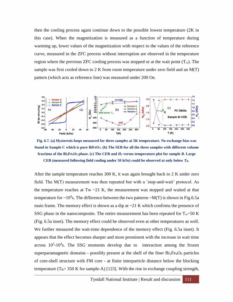
Tyndall National Institute | Result and discussion 111
then the cooling process again continue down to the possible lowest temperature (2K in
this case). When the magnetization is measured as a function of temperature during
warming up, lower values of the magnetization with respect to the values of the reference
curve, measured in the ZFC process without interruption are observed in the temperature
region where the previous ZFC cooling process was stopped or at the wait point (Tw). The
sample was first cooled down to 2 K from room temperature under zero field and an M(T)
pattern (which acts as reference line) was measured under 200 Oe.
Fig. 6.7. (a) Hysteresis loops measured for three samples at 5K temperature. No exchange bias was
found in Sample C which is pure BiFeO3. (b) The SEB for all the three samples with different volume
fractions of the Bi2Fe4O9 phase. (c) The CEB and HC versus temperature plot for sample B. Large
CEB (measured following field cooling under 50 kOe) could be observed at only below TB.
After the sample temperature reaches 300 K, it was again brought back to 2 K under zero
field. The M(T) measurement was then repeated but with a ’stop-and-wait’ protocol. As
the temperature reaches at Tw ~21 K, the measurement was stopped and waited at that
temperature for ~104s. The difference between the two patterns ~M(T) is shown in Fig.6.5a
main frame. The memory effect is shown as a dip at ~21 K which confirms the presence of
SSG phase in the nanocomposite. The entire measurement has been repeated for Tw~50 K
(Fig. 6.5a inset). The memory effect could be observed even at other temperatures as well.
We further measured the wait-time dependence of the memory effect (Fig. 6.5a inset). It
appears that the effect becomes sharper and more prominent with the increase in wait time
across 103-104s. The SSG moments develop due to interaction among the frozen
superparamagnetic domains - possibly present at the shell of the finer Bi2Fe4O9 particles
of core-shell structure with FM core - at finite interparticle distance below the blocking
temperature (TB> 350 K for sample-A) [123]. With the rise in exchange coupling strength,
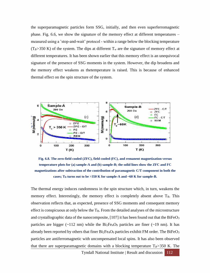
Tyndall National Institute | Result and discussion 112
the superparamagnetic particles form SSG, initially, and then even superferromagnetic
phase. Fig. 6.6, we show the signature of the memory effect at different temperatures –
measured using a ’stop-and-wait’ protocol - within a range below the blocking temperature
(TB>350 K) of the system. The dips at different Tw are the signature of memory effect at
different temperatures. It has been shown earlier that this memory effect is an unequivocal
signature of the presence of SSG moments in the system. However, the dip broadens and
the memory effect weakens as thetemperature is raised. This is because of enhanced
thermal effect on the spin structure of the system.
Fig. 6.8. The zero-field cooled (ZFC), field cooled (FC), and remanent magnetization versus
temperature plots for (a) sample-A and (b) sample-B; the solid lines show the ZFC and FC
magnetizations after subtraction of the contribution of paramagnetic C/T component in both the
cases; TB turns out to be >350 K for sample-A and ~60 K for sample-B.
The thermal energy induces randomness in the spin structure which, in turn, weakens the
memory effect. Interestingly, the memory effect is completely absent above TB. This
observation reflects that, as expected, presence of SSG moments and consequent memory
effect is conspicuous at only below the TB. From the detailed analyses of the microstructure
and crystallographic data of the nanocomposite, [107] it has been found out that the BiFeO3
particles are bigger (~112 nm) while the Bi2Fe4O9 particles are finer (~19 nm). It has
already been reported by others that finer Bi2Fe4O9 particles exhibit FM order. The BiFeO3
particles are antiferromagnetic with uncompensated local spins. It has also been observed
that there are superparamagnetic domains with a blocking temperature TB>350 K. The
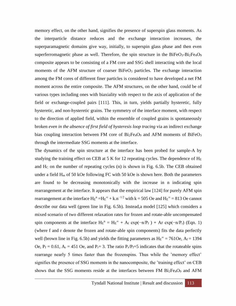
Tyndall National Institute | Result and discussion 113
memory effect, on the other hand, signifies the presence of superspin glass moments. As
the interparticle distance reduces and the exchange interaction increases, the
superparamagnetic domains give way, initially, to superspin glass phase and then even
superferromagnetic phase as well. Therefore, the spin structure in the BiFeO3-Bi2Fe4O9
composite appears to be consisting of a FM core and SSG shell interacting with the local
moments of the AFM structure of coarser BiFeO3 particles. The exchange interaction
among the FM cores of different finer particles is considered to have developed a net FM
moment across the entire composite. The AFM structures, on the other hand, could be of
various types including ones with biaxiality with respect to the axis of application of the
field or exchange-coupled pairs [111]. This, in turn, yields partially hysteretic, fully
hysteretic, and non-hysteretic grains. The symmetry of the interface moment, with respect
to the direction of applied field, within the ensemble of coupled grains is spontaneously
broken even in the absence of first field of hysteresis loop tracing via an indirect exchange
bias coupling interaction between FM core of Bi2Fe4O9 and AFM moments of BiFeO3
through the intermediate SSG moments at the interface.
The dynamics of the spin structure at the interface has been probed for sample-A by
studying the training effect on CEB at 5 K for 12 repeating cycles. The dependence of HE
and HC on the number of repeating cycles (n) is shown in Fig. 6.5b. The CEB obtained
under a field Hm of 50 kOe following FC with 50 kOe is shown here. Both the parameters
are found to be decreasing monotonically with the increase in n indicating spin
rearrangement at the interface. It appears that the empirical law [124] for purely AFM spin
rearrangement at the interface HEn =HE
∞ + k.n−1/2 with k = 505 Oe and HE∞ = 813 Oe cannot
describe our data well (green line in Fig. 6.5b). Instead,a model [125] which considers a
mixed scenario of two different relaxation rates for frozen and rotate-able uncompensated
spin components at the interface HEn = HE
∞ + Af exp(−n/Pf ) + Ar exp(−n/Pr) (Eqn. 1)
(where f and r denote the frozen and rotate-able spin components) fits the data perfectly
well (brown line in Fig. 6.5b) and yields the fitting parameters as HE∞ = 761Oe, Af = 1394
Oe, Pf = 0.61, Ar = 451 Oe, and Pr= 3. The ratio Pr/Pf=5 indicates that the rotateable spins
rearrange nearly 5 times faster than the frozenspins. Thus while the ’memory effect’
signifies the presence of SSG moments in the nanocomposite, the ’training effect’ on CEB
shows that the SSG moments reside at the interfaces between FM Bi2Fe4O9 and AFM
Tyndall National Institute | Result and discussion 114
BiFeO3 particles and influence the SEB and CEB significantly. It is important to mention
here that the SEB exhibits negligible training effect within the laboratory time scale
(~104s). This could be because it originates from a stable state under zero field and zero
magnetization through spontaneous symmetry breaking.
We further examined the SEB in two other samples with higher (~10%) and lower (<3%)
volume fraction of Bi2Fe4O9 (sample-B and C, respectively). The corresponding full
hysteresis loops have been shown in Figure 6.7a. The TN of the AFM component for
sample-B and C are ~490 K and ~450 K, respectively. In Fig. 6.7a, comparison of the
hysteresis loops among all the three samples (A, B, and C) and in Fig.6.7b SEB are
shown.The SEB is found to follow a rather nonmonotonic pattern with the variation in the
volume fraction of Bi2Fe4O9 phase. It decreases both with the increase and decrease in the
volume fraction of the Bi2Fe4O9 phase. The SEB in all these cases could be observed at
only below the respective TB. The TB decreases down to ~60 K in sample-B because of
finer Bi2Fe4O9 particles (~8 nm). The TB, however, could
Fig. 6.9. Schematic of the ferromagnetic and antiferromagnetic spin interaction via superspin glass
moments at the interface; left part shows the ferromagnetic core of finer Bi2Fe4O9 particle and
superspin glass moments at the shell interacting with the local moments of spiral spin spin structure
of bigger BiFeO3; right part shows the spin configuration and interaction energies.
Tyndall National Institute | Result and discussion 115
not be located within the range 5-300 K for sample-C and, therefore, no exchange bias
could be observed in this sample within the same temperature range. The CEB and HC for
sample-B are also found to be finite (Fig. 6.7 c) only at below the TB (~60K). And as
expected, the memory effect too has been observed in sample-B at below TB. The memory
effect, observed both in sample-A and B, implies presence of SSG phase and its influence
on the exchange bias. Since superparamagnetic and SSG phases coexist at below TB in both
the samples, one can estimate the relative volume fraction of the SSG phase by calculating
the ZFC and FC magnetic moment versus temperature pattern after subtracting the
contribution of Curie paramagnetic component C/T (C = Curie constant) from the
experimental result (Figs 6.8 a and b) and noting the flatness of the FC moment versus
temperature pattern [125] at below TB. The calculated patterns (solid lines) for both the
samples A and B are shown in Figs. 6.8 a & b, respectively. It appears that the volume
fraction of SSG phase is higher in sample-A than in sample-B. The SEB too is higher in
sample-A than in sample-B. Clear correlation between the volume fraction of the SSG
phase and the extent of SEB shows that the SSG phase plays a major role in inducing SEB.
We show that all these results could be qualitatively understood by considering a model of
”superinteraction bias coupling” between the superspin of superparamagnetic core of finer
Bi2Fe4O9 and local uncompensated moments of the AFM order in coarser BiFeO3 particles
via SSG shell at the interface. The model is shown schematically in Fig. 6.9 and draws
essentially from the model proposed in Ref. 112. The dotted line marks the direction of the
applied field. The shell SSG moments s1 and s2 are coupled to the FM moment SF by a
coupling parameter JF and to the AFM moment SAF by JAF while the coupling between s1
and s2 is J. The net coupling parameter b will depend on JAF, JF, and J and, finally, HE / b
[114]. It has been shown [114] that the random fields generated by spin glass moments at
the core can act on the saturated FM moment and set the UA via RKKY interaction. The
model that we are proposing in the present case is the following. The random field from
frozen SSG moments appears to be inducing a variation in the anisotropy of the AFM
moments including biaxiality with respect to the direction of the applied field. Thus
depending on the orientation of the principal easy axes of AFM grains with respect to the
direction of the applied field, the AFM grains can experience either no torque or large
torque. Accodingly AFM grains set the UA, primarily, in a direction opposite to that of the
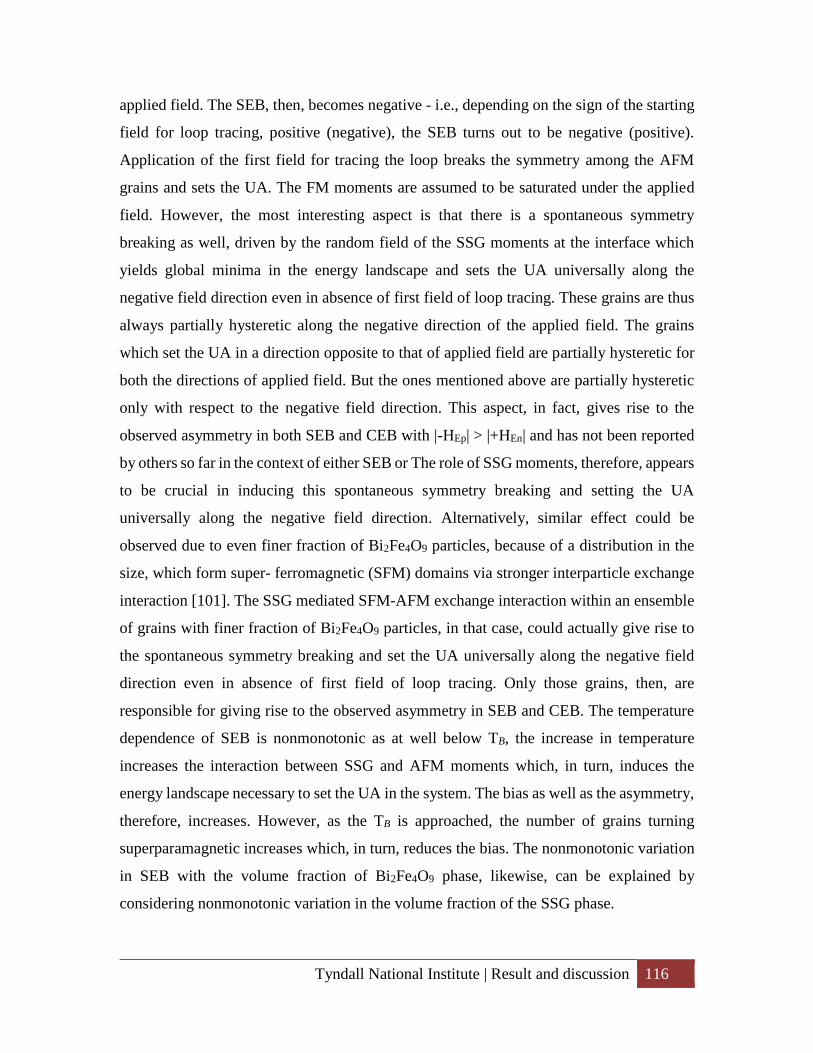
Tyndall National Institute | Result and discussion 116
applied field. The SEB, then, becomes negative - i.e., depending on the sign of the starting
field for loop tracing, positive (negative), the SEB turns out to be negative (positive).
Application of the first field for tracing the loop breaks the symmetry among the AFM
grains and sets the UA. The FM moments are assumed to be saturated under the applied
field. However, the most interesting aspect is that there is a spontaneous symmetry
breaking as well, driven by the random field of the SSG moments at the interface which
yields global minima in the energy landscape and sets the UA universally along the
negative field direction even in absence of first field of loop tracing. These grains are thus
always partially hysteretic along the negative direction of the applied field. The grains
which set the UA in a direction opposite to that of applied field are partially hysteretic for
both the directions of applied field. But the ones mentioned above are partially hysteretic
only with respect to the negative field direction. This aspect, in fact, gives rise to the
observed asymmetry in both SEB and CEB with |-HEp| > |+HEn| and has not been reported
by others so far in the context of either SEB or The role of SSG moments, therefore, appears
to be crucial in inducing this spontaneous symmetry breaking and setting the UA
universally along the negative field direction. Alternatively, similar effect could be
observed due to even finer fraction of Bi2Fe4O9 particles, because of a distribution in the
size, which form super- ferromagnetic (SFM) domains via stronger interparticle exchange
interaction [101]. The SSG mediated SFM-AFM exchange interaction within an ensemble
of grains with finer fraction of Bi2Fe4O9 particles, in that case, could actually give rise to
the spontaneous symmetry breaking and set the UA universally along the negative field
direction even in absence of first field of loop tracing. Only those grains, then, are
responsible for giving rise to the observed asymmetry in SEB and CEB. The temperature
dependence of SEB is nonmonotonic as at well below TB, the increase in temperature
increases the interaction between SSG and AFM moments which, in turn, induces the
energy landscape necessary to set the UA in the system. The bias as well as the asymmetry,
therefore, increases. However, as the TB is approached, the number of grains turning
superparamagnetic increases which, in turn, reduces the bias. The nonmonotonic variation
in SEB with the volume fraction of Bi2Fe4O9 phase, likewise, can be explained by
considering nonmonotonic variation in the volume fraction of the SSG phase.
Tyndall National Institute | Result and discussion 117
The tunable spontaneous exchange bias of ~300-600 Oe across 5-300 K in nanocomposite
of BiFeO3 (~94%) - Bi2Fe4O9 (~6%)(Sample A) originates from a superinteraction bias
coupling between ferromagnetic core of finer Bi2Fe4O9 (~19 nm)
Fig. 6.10. The path dependency of (a) spontaneous exchange bias and (b) corresponding coercivity as
a function of temperature; the path dependency of (c) conventional exchange bias and (d)
corresponding coercivity as a function of temperature.
Tyndall National Institute | Result and discussion 118
particles and antiferromagnetic moment in coarser (~112 nm) BiFeO3 particles via
superspin glass moments at the interface. Since it induces a variety of coupling across the
interfaces and thus develops a complicated interaction energy landscape among the
FM/AFM grains by breaking the symmetry spontaneously even in the absence of first field
of loop tracing, the presence of superspin glass moments turns out to be crucial. This giant
and tunable (i.e., path dependent) exchange bias can be utilized for an enormous
improvement in the efficiency of switching the magnetic anisotropy in a ferromagnetic
system electrically via “exchange coupling mediated multiferroicity” in such a
nanocomposite and/or a multilayer thin film systems.
While the conventional exchange bias (CEB) is observed under field cooling which sets
the unidirectional anisotropy across a ferromagnet (FM) – antiferromagnet (AFM)
interface prior to the measurement of the hysteresis loop, the spontaneous one is observed
even in an unmagnetized state following zero-field cooling. It results from a symmetry
breaking across the FM-AFM interfaces and setting of the unidirectional anisotropy (UA)
under the first field of the hysteresis loop tracing. In recent times, the spontaneous exchange
bias (SEB) has been reported for different alloy and nanoparticle composite systems [111].
The origin of this appears to be lying in the biaxiality of AFM grains and variation in the
FM-AFM bias coupling among an ensemble of grains. We have observed an even more
interesting feature of the SEB - variation in the magnitude of the bias depending on the
path followed in tracing the hysteresis loop - in a nanocomposite of BiFeO3-Bi2Fe4O9. The
hysteresis loop has been traced following two paths - +Hmax→-Hmax →+Hmax (path a)
and -Hmax →+Hmax →-Hmax (path b); Hmax is the maximum field applied for tracing
the loop. This asymmetry in the SEB offers an additional tunability apart from the
magnitude of the maximum field itself and has not been reported for any other composite
or multilayer system exhibiting exchange bias. We have also measured the CEB and found
that CEB too, exhibits such a path dependency. The asymmetry in the SEB and CEB -
ΔHSEB and ΔHCEB – is found to be temperature dependent; while ΔHSEB decreases with
temperature nonmonotonically the ΔHCEB decreases rather monotonically. We have found
that the SEB, CEB and their path dependency are originating from a spontaneous breaking
of the symmetry of interface magnetic moment and setting of UA among an ensemble of
FM and AFM particles even in the absence of first field of hysteresis as a result of superspin
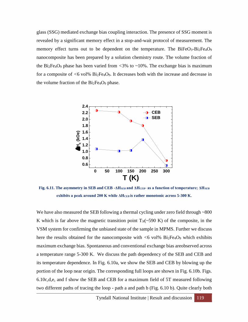
Tyndall National Institute | Result and discussion 119
glass (SSG) mediated exchange bias coupling interaction. The presence of SSG moment is
revealed by a significant memory effect in a stop-and-wait protocol of measurement. The
memory effect turns out to be dependent on the temperature. The BiFeO3-Bi2Fe4O9
nanocomposite has been prepared by a solution chemistry route. The volume fraction of
the Bi2Fe4O9 phase has been varied from <3% to ~10%. The exchange bias is maximum
for a composite of <6 vol% Bi2Fe4O9. It decreases both with the increase and decrease in
the volume fraction of the Bi2Fe4O9 phase.
0 50 100 150 200 250 300
0.6
0.8
1.0
1.2
1.4
1.6
1.8
2.0
2.2
2.4
H
E (
kO
e)
T (K)
CEB
SEB
Fig. 6.11. The asymmetry in SEB and CEB -ΔHSEB and ΔHCEB- as a function of temperature; ΔHSEB
exhibits a peak around 200 K while ΔHCEB is rather monotonic across 5-300 K.
We have also measured the SEB following a thermal cycling under zero field through ~800
K which is far above the magnetic transition point TN(~590 K) of the composite, in the
VSM system for confirming the unbiased state of the sample in MPMS. Further we discuss
here the results obtained for the nanocomposite with <6 vol% Bi2Fe4O9 which exhibits
maximum exchange bias. Spontaneous and conventional exchange bias areobserved across
a temperature range 5-300 K. We discuss the path dependency of the SEB and CEB and
its temperature dependence. In Fig. 6.10a, we show the SEB and CEB by blowing up the
portion of the loop near origin. The corresponding full loops are shown in Fig. 6.10b. Figs.
6.10c,d,e, and f show the SEB and CEB for a maximum field of 5T measured following
two different paths of tracing the loop - path a and path b (Fig. 6.10 b). Quite clearly both
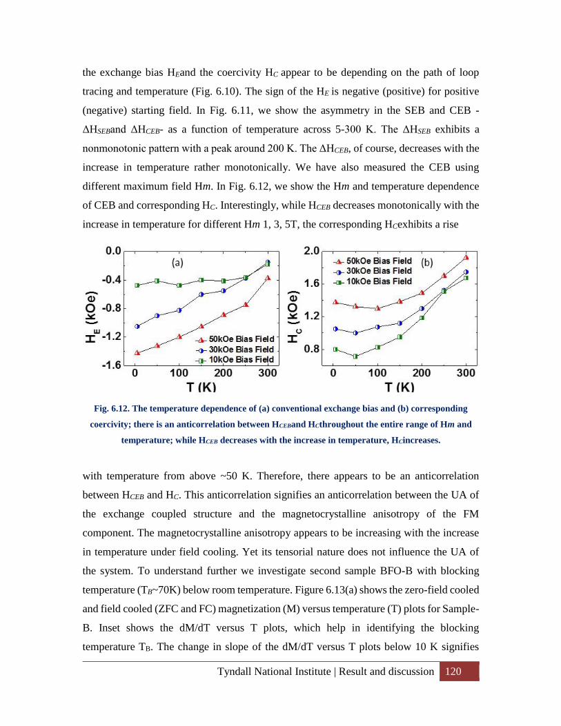
Tyndall National Institute | Result and discussion 120
the exchange bias HEand the coercivity HC appear to be depending on the path of loop
tracing and temperature (Fig. 6.10). The sign of the HE is negative (positive) for positive
(negative) starting field. In Fig. 6.11, we show the asymmetry in the SEB and CEB -
ΔHSEBand ΔHCEB- as a function of temperature across 5-300 K. The ΔHSEB exhibits a
nonmonotonic pattern with a peak around 200 K. The ΔHCEB, of course, decreases with the
increase in temperature rather monotonically. We have also measured the CEB using
different maximum field Hm. In Fig. 6.12, we show the Hm and temperature dependence
of CEB and corresponding HC. Interestingly, while HCEB decreases monotonically with the
increase in temperature for different Hm 1, 3, 5T, the corresponding HCexhibits a rise
Fig. 6.12. The temperature dependence of (a) conventional exchange bias and (b) corresponding
coercivity; there is an anticorrelation between HCEBand HCthroughout the entire range of Hm and
temperature; while HCEB decreases with the increase in temperature, HCincreases.
with temperature from above ~50 K. Therefore, there appears to be an anticorrelation
between HCEB and HC. This anticorrelation signifies an anticorrelation between the UA of
the exchange coupled structure and the magnetocrystalline anisotropy of the FM
component. The magnetocrystalline anisotropy appears to be increasing with the increase
in temperature under field cooling. Yet its tensorial nature does not influence the UA of
the system. To understand further we investigate second sample BFO-B with blocking
temperature (TB~70K) below room temperature. Figure 6.13(a) shows the zero-field cooled
and field cooled (ZFC and FC) magnetization (M) versus temperature (T) plots for Sample-
B. Inset shows the dM/dT versus T plots, which help in identifying the blocking
temperature TB. The change in slope of the dM/dT versus T plots below 10 K signifies
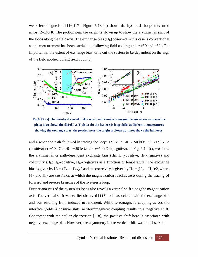
Tyndall National Institute | Result and discussion 121
weak ferromagnetism [116,117]. Figure 6.13 (b) shows the hysteresis loops measured
across 2–100 K. The portion near the origin is blown up to show the asymmetric shift of
the loops along the field axis. The exchange bias (HE) observed in this case is conventional
as the measurement has been carried out following field cooling under +50 and −50 kOe.
Importantly, the extent of exchange bias turns out the system to be dependent on the sign
of the field applied during field cooling
Fig.6.13. (a) The zero-field cooled, field-cooled, and remanent magnetization versus temperature
plots; inset shows the dM/dT vs T plots; (b) the hysteresis loop shifts at different temperatures
showing the exchange bias; the portion near the origin is blown up; inset shows the full loops.
and also on the path followed in tracing the loop: +50 kOe→0→−50 kOe→0→+50 kOe
(positive) or −50 kOe→0→+50 kOe→0→−50 kOe (negative). In Fig. 6.14 (a), we show
the asymmetric or path-dependent exchange bias (HE: HEp-positive, HEn-negative) and
coercivity (HC: HCp-positive, HCn-negative) as a function of temperature. The exchange
bias is given by HE = (Hc1 + Hc2)/2 and the coercivity is given by HC = (Hc1 − Hc2)/2, where
Hc1 and Hc2 are the fields at which the magnetization reaches zero during the tracing of
forward and reverse branches of the hysteresis loop.
Further analysis of the hysteresis loops also reveals a vertical shift along the magnetization
axis. The vertical shift was earlier observed [118] to be associated with the exchange bias
and was resulting from induced net moment. While ferromagnetic coupling across the
interface yields a positive shift, antiferromagnetic coupling results in a negative shift.
Consistent with the earlier observation [118], the positive shift here is associated with
negative exchange bias. However, the asymmetry in the vertical shift was not observed
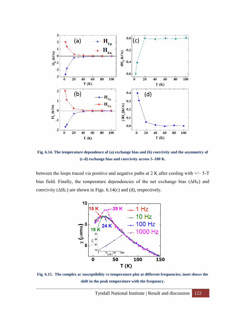
Tyndall National Institute | Result and discussion 122
Fig. 6.14. The temperature dependence of (a) exchange bias and (b) coercivity and the asymmetry of
(c-d) exchange bias and coercivity across 5–100 K.
between the loops traced via positive and negative paths at 2 K after cooling with +/− 5-T
bias field. Finally, the temperature dependencies of the net exchange bias (ΔHE) and
coercivity (ΔHC) are shown in Figs. 6.14(c) and (d), respectively.
Fig. 6.15. The complex ac susceptibility vs temperature plot at different frequencies; inset shows the
shift in the peak temperature with the frequency.
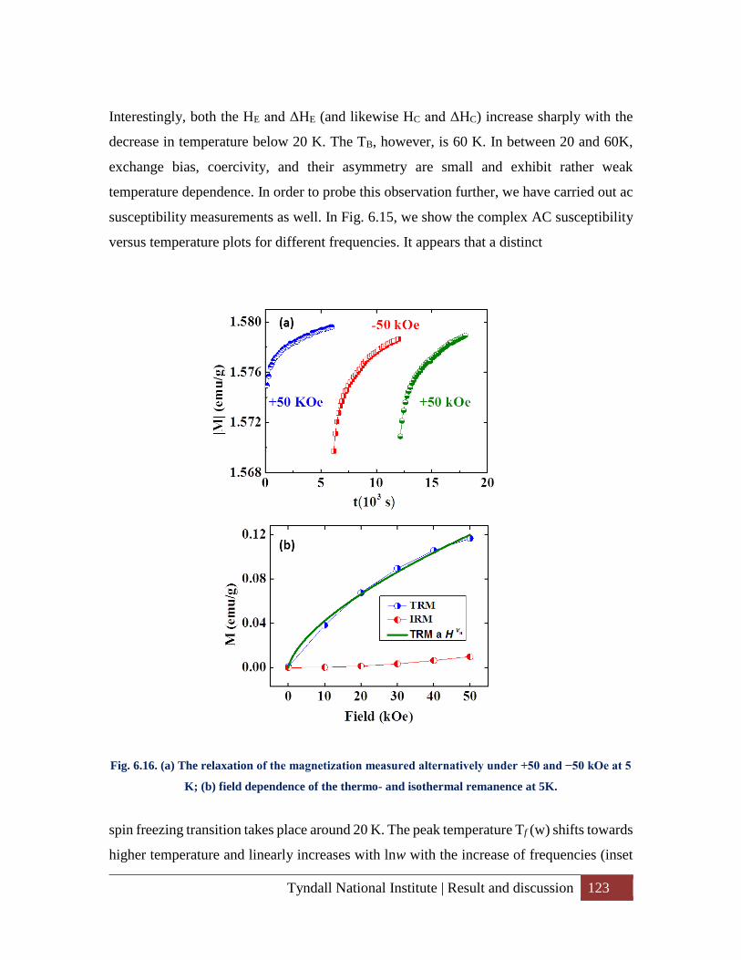
Tyndall National Institute | Result and discussion 123
Interestingly, both the HE and ΔHE (and likewise HC and ΔHC) increase sharply with the
decrease in temperature below 20 K. The TB, however, is 60 K. In between 20 and 60K,
exchange bias, coercivity, and their asymmetry are small and exhibit rather weak
temperature dependence. In order to probe this observation further, we have carried out ac
susceptibility measurements as well. In Fig. 6.15, we show the complex AC susceptibility
versus temperature plots for different frequencies. It appears that a distinct
Fig. 6.16. (a) The relaxation of the magnetization measured alternatively under +50 and −50 kOe at 5
K; (b) field dependence of the thermo- and isothermal remanence at 5K.
spin freezing transition takes place around 20 K. The peak temperature Tf (w) shifts towards
higher temperature and linearly increases with lnw with the increase of frequencies (inset
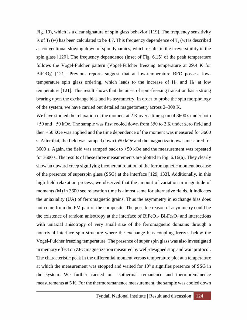
Tyndall National Institute | Result and discussion 124
Fig. 10), which is a clear signature of spin glass behavior [119]. The frequency sensitivity
K of Tf (w) has been calculated to be 4.7. This frequency dependence of Tf (w) is described
as conventional slowing down of spin dynamics, which results in the irreversibility in the
spin glass [120]. The frequency dependence (inset of Fig. 6.15) of the peak temperature
follows the Vogel-Fulcher pattern (Vogel-Fulcher freezing temperature at 29.4 K for
BiFeO3) [121]. Previous reports suggest that at low-temperature BFO possess low-
temperature spin glass ordering, which leads to the increase of HB and HC at low
temperature [121]. This result shows that the onset of spin-freezing transition has a strong
bearing upon the exchange bias and its asymmetry. In order to probe the spin morphology
of the system, we have carried out detailed magnetometry across 2–300 K.
We have studied the relaxation of the moment at 2 K over a time span of 3600 s under both
+50 and −50 kOe. The sample was first cooled down from 350 to 2 K under zero field and
then +50 kOe was applied and the time dependence of the moment was measured for 3600
s. After that, the field was ramped down to50 kOe and the magnetizationwas measured for
3600 s. Again, the field was ramped back to +50 kOe and the measurement was repeated
for 3600 s. The results of these three measurements are plotted in Fig. 6.16(a). They clearly
show an upward creep signifying incoherent rotation of the ferromagnetic moment because
of the presence of superspin glass (SSG) at the interface [129, 133]. Additionally, in this
high field relaxation process, we observed that the amount of variation in magnitude of
moments (M) in 3600 sec relaxation time is almost same for alternative fields. It indicates
the uniaxiality (UA) of ferromagnetic grains. Thus the asymmetry in exchange bias does
not come from the FM part of the composite. The possible reason of asymmetry could be
the existence of random anisotropy at the interface of BiFeO3- Bi2Fe4O9 and interactions
with uniaxial anisotropy of very small size of the ferromagnetic domains through a
nontrivial interface spin structure where the exchange bias coupling freezes below the
Vogel-Fulcher freezing temperature. The presence of super spin glass was also investigated
in memory effect on ZFC magnetization measured by well-designed stop and wait protocol.
The characteristic peak in the differential moment versus temperature plot at a temperature
at which the measurement was stopped and waited for 104 s signifies presence of SSG in
the system. We further carried out isothermal remanence and thermoremanence
measurements at 5 K. For the thermoremanence measurement, the sample was cooled down
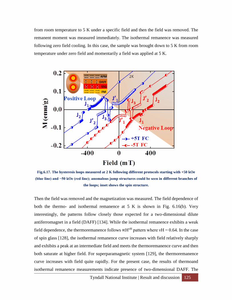
Tyndall National Institute | Result and discussion 125
from room temperature to 5 K under a specific field and then the field was removed. The
remanent moment was measured immediately. The isothermal remanence was measured
following zero field cooling. In this case, the sample was brought down to 5 K from room
temperature under zero field and momentarily a field was applied at 5 K.
Fig.6.17. The hysteresis loops measured at 2 K following different protocols starting with +50 kOe
(blue line) and −50 kOe (red line); anomalous jump structures could be seen in different branches of
the loops; inset shows the spin structure.
Then the field was removed and the magnetization was measured. The field dependence of
both the thermo- and isothermal remanence at 5 K is shown in Fig. 6.16(b). Very
interestingly, the patterns follow closely those expected for a two-dimensional dilute
antiferromagnet in a field (DAFF) [134]. While the isothermal remanence exhibits a weak
field dependence, the thermoremanence follows ∝HνH pattern where νH = 0.64. In the case
of spin glass [128], the isothermal remanence curve increases with field relatively sharply
and exhibits a peak at an intermediate field and meets the thermoremanence curve and then
both saturate at higher field. For superparamagnetic system [129], the thermoremanence
curve increases with field quite rapidly. For the present case, the results of thermoand
isothermal remanence measurements indicate presence of two-dimensional DAFF. The
Tyndall National Institute | Result and discussion 126
high-field relaxation process and memory effect on ZFC magnetization, on the other hand,
signify simultaneous presence of SSG. The overall spin morphology, therefore, appears to
be consisting of four components: ferromagnetic (FM) and antiferromagnetic (AFM) cores
and interfaces vitiated by SSG and DAFF shells.
Finally, we have measured the hysteresis loops with higher resolution at 2 K starting from
+50 kOe and from −50 kOe. The loops, especially the portion near the origin, are shown in
Fig. 6.17. Quite conspicuous are the sharp jumps in the loops. Such jumps have earlier been
observed in systems containing inhomogeneities and thus random anisotropy [130-132]. In
fact, both by experimental and theoretical work, it has been shown that depending on the
strength of the random anisotropy with respect to the exchange coupling, several jumps
might be seen in hysteresis loops at low temperature. Because of thermal perturbation, they
smear off at higher temperature. In the present case too, loops measured at higher
temperature (5 K) exhibit lesser number of jumps and complete smearing off eventually at
temperature higher than that. However, there is an interesting distinction between the jumps
observed in a ferromagnetic system containing purely random anisotropy because of
inhomogeneities and the jumps observed here. The number of jumps observed, in the
present case are different in two different branches of a particular loop. The inversion
symmetry, normally observed in systems containing purely random anisotropy [131], is
broken here. While lesser jumps (J1,J2) could be seen in the forward branch, more
jumps(J1,J2,J3) are conspicuous in the reverse branch (Fig. 6.15). This is true for both the
loops—whether the loop has been traced starting from+50 or−50 kOe. There is, however,
conspicuous inversion symmetry in the jump structure in between two forward and two
reverse branches of the loops traced starting from +50 and −50 kOe. It is possible to notice
that the branch on the extreme left (blue line) is a mirror image of the branch on the extreme
right (red line) of Fig. 6.17. Likewise, the inner blue and red branches are also mirror
images of each other. Such an asymmetric pattern of jumps for a particular loop yet a
symmetric one between the loops traced via two different protocols is remarkable and has
not been reported earlier. This observation clearly points out that there could be a
correlation between this symmetry of the jump pattern and the protocol dependency of the
exchange bias. It has been argued below that these results from a local topological spin
texture at the interface which, in turn, gives rise to a strong universal unidirectional
Tyndall National Institute | Result and discussion 127
anisotropy of the interface moment along negative field direction. It has been shown that
random anisotropy due to inhomogeneities leads to jumps in the hysteresis loop at a very
low temperature (100–500 mK) as a result of avalanches in domain flipping.[132] The
random anisotropy field competes with the applied field and as and when the spins are
aligned with the local anisotropy, the avalanche takes place. The role of local anisotropy
has been addressed both by site-centric local random field model [130] as well as cluster
model [132]. The Hamiltonian considers the exchange coupling among the spins, local
random field due to anisotropy, and the applied field.
In the case of the present system, exhibiting exchange bias, exchange coupling interaction
across the interface between the BiFeO3 and Bi2Fe4O9 particles should also be
considered.This is strongly influenced by the SSG and DAFF layers at the interface. While
BiFeO3 crystallizes in rhombohedral structure with R3c space group, Bi2Fe4O9 crystallizes
in orthorhombic structure with Pbam space group. The interface, therefore, creates a certain
topology that induces, at least, a local spin texture even though globally the salient features
of the SSG and DAFF are retained. Therefore, in presence of such local spin texture, both
random and textured anisotropy fields compete with the applied field and the exchange
coupling interaction across the interface. The domain flipping and avalanche along two
different pathways is not identically influenced. The textured anisotropy creates a self-
generating interfacial moment, which acts upon the exchange coupling interaction in
between BiFeO3 and Bi2Fe4O9 and sets the universal unidirectional anisotropy along the
negative direction of the applied field. This loss of randomness and preferred orientation
of the local anisotropy breaks the inversion symmetry of the jump structure in the hysteresis
loop. The net interface moment from this textured anisotropy and development of
unidirectional anisotropy of the interface moment toward negative direction of the applied
field as a consequence lies at the heart of the path dependency of exchange bias. In fact,
this asymmetric jump structure in the hysteresis loop at 2 K is the first clear proof of the
presence of textured pattern of anisotropy at the interface between ferromagnetic and
antiferromagnetic cores which appears to generate the self-generating interface moment
along a preferred direction with respect to the direction of the applied field. Topological
spin texture in the form of magnetic vortices carrying an electric charge (skyrmion) could
earlier be identified in chiral lattice system [133]. The random as well as the textured
Tyndall National Institute | Result and discussion 128
anisotropy is strong enough as their influence on the hysteresis loop could be seen at a
temperature as high as 2 K. In other ferromagnetic systems with local inhomogeneity [132],
influence of random anisotropy could be seen at even lower temperature (100–500 mK). It
is also important to mention here that the influence of this local spin texture in inducing a
net interface moment is observable only below the spin freezing temperature, i.e., the
Vogel-Fulcher freezing temperature at 29.4 K for BiFeO3. The spin structure at the
interface needs to be frozen in order to create strong local field. As the temperature is raised
toward∼29.4 K from below, influence of the interface spin morphology as well as the net
interface moment weaken and so the exchange bias and its path dependency.
This spontaneous setting of UA along the negative direction of applied field (or universal
UA) even under zero field is the origin of the path dependency for both SEB and CEB. The
volume fraction of the partially hysteretic grains 𝑉𝑓𝑔𝑈𝑈𝐴 with universal UA (UUA) along the
negative direction of the applied field governs the magnitude of exchange bias as well as
its path dependency. The volume fraction of the partially hysteretic grains𝑉𝑓𝑔𝑈𝐴 with UA set
by the first field of the loop tracing, on the other hand, governs the magnitudeof exchange
bias but not the path dependency. The temperature dependences of 𝑉𝑓𝑔𝑈𝑈𝐴(T) and 𝑉𝑓𝑔
𝑈𝐴(T)
and their subtle interplay influence the temperature dependence of ΔHSEB and HSEB. The
nonmonotonicity in both HSEB and ΔHSEB possibly results from an initial increase in
𝑉𝑓𝑔𝑈𝑈𝐴and 𝑉𝑓𝑔
𝑈𝐴 with temperature due to an increase in SSG mediated indirect exchange bias
coupling amongthe grains. As the temperature increases, the frozenmoments of SSG at the
shell in between FM and AFM grains are thermally activated to interact strongly withthe
FM and AFM moments. This strong interaction, inturn, makes the spontaneous symmetry
breaking moreeffective and gives rise to enhanced path dependencyin SEB. With further
rise in temperature, the 𝑉𝑓𝑔𝑈𝑈𝐴 eventually decreases as enhanced thermal randomization of
the spin structure itself results in weakening of bias coupling interaction. This anomalous
influence of temperature is not conspicuous in the case of CEB as in this case both the
UUA and UA are further influenced by field cooling from higher temperature. The
impactof field cooling masks the subtle role of temperatureon SSG induced spontaneous
setting of UA. In fact, as shown in Fig. 6.10, apart from its path dependency, the CEB itself
does not exhibit any nonmonotonicity across 5-300 K.The ΔHSEB and ΔHCEB offer an
Tyndall National Institute | Summary 129
additional tenability to the exchange bias. Using a combination of maximumfield of loop
tracing (Hm) as well as the path followed intracing the loop - positive or negative - it is
possible totune the magnitude of the exchange bias. This tunability, in turn, can increase
the functionality in electrically switching the magnetic anisotropy of a ferromagnetic
systemin a BiFeO3-ferromagnetic composite like the present one via multiferroic coupling
between ferroelectric polarization and magnetization in BiFeO3.
6.5. Summary
In summary, we report that in a nanocomposite of (~94 vol %) BiFeO3-(~6 vol%) Bi2Fe4O9
with finer and ferromagnetic Bi2Fe4O9 particles and coarser and antiferromagnetic BiFeO3,
one observes a large and path-dependent spontaneous exchange bias (~30-60 mT) across
5-300 K. The conventional exchange bias too is found to be path dependent. This path
dependency offers an additional tunability in the effect of electrical switching of magnetic
anisotropy in a BiFeO3-ferromagnetic composite via multiferroic coupling and is expected
to improve the functionality of such a device enormously. The net interface moment from
textured anisotropy and consequent path dependency of the exchange bias is quite an
attractive proposition as it offers tunability to the exchange bias depending on the path
followed in tracing the hysteresis loop. Since BiFeO3 is a well-known room temperature
multiferroic, it is possible to switch the magnetic anisotropy of the ferromagnetic
component by applying electric field. Tunable exchange bias then helps in tuning the extent
of switching and thus increases the functionality manyfold. In summary, we show that a
textured pattern of magnetic anisotropy forms at the interface between ferromagnetic
Bi2Fe4O9 and antiferromagnetic BiFeO3 nanoparticles from shells of superspin glass and
dilute antiferromagnet in a field. The local field from this texture generates net interface
moment to set the unidirectional anisotropy along a preferred direction with respect to the
direction of the applied field. Such a spontaneous onset of nonswitchable unidirectional
anisotropy under field appears to be the origin of the path dependency of the exchange bias.
The textured anisotropy at the interface also yields an asymmetric pattern of sharp jumps
in the hysteresis loop at low temperature. Thus a direct correlation could be established
between the asymmetric jump structure in the hysteresis loop at low temperature and the

Tyndall National Institute | Summary 130
path dependency of the exchange bias. Instead of a “clean” interface between
ferromagnetic and antiferromagnetic grains, an interface with coexisting local spin texture
and random anisotropy emerging out of superspin glass and dilute antiferromagnet in a
field, therefore, offers a rare tunability to the exchange bias via its path dependency and,
thereby, increases its utility for device applications many fold.
Tyndall National Institute | Chapter - Tunable inverted hysterisis loop 131
7. Chapter - Tunable inverted hysterisis loop
7.1. Introduction:
In magnetism the shift of hysteresis loop, so called exchange bias (EB) was first observed
by Meiklejohn and Bean [18] in ferromagnetic (FM) Co particle encapsulated with
antiferromagnetic (AFM) CoO. For more than a half century this phenomena has been
studied due to its potential applications in giant magneto resistance (GMR) [134], spin
valve [135], high density storage media [136] etc. as well as for fundamental studies. The
conventional way to induce exchange anisotropy, named exchange bias (EB) is to cool
down a magnetically uncompensated AFM-FM interface below Nee´l Temperature (TN) of
AMF and Curie Temperature (TC) of FM where TN<TC. A unidirectional shift of hysterics
or exchange bias should be observed in exchanges coupled FM-AFM interface. In most
cases the exchange bias is observed in the direction of cooling field, which is called positive
EB. Due to the AFM-FM interaction, the FM spins intend to point in the direction of the
cooling field at low temperatures below TN. In some cases due to the large unidirectional
anisotropy of AFM, the AFM-FM interfacial interaction biases FM spins to the opposite
direction of cooling field and causes a loop shift in opposite direction causing negative
exchange bias. In addition an enhancement of coercivity is also observed [21-24].
However, for large cooling field the same sample provide positive exchange bias where
this large cooling field is required to reverse the magnetically easy direction of the
unidirectional anisotropy to produce positive exchange bias in pure metal or metal-fluoride
materials. [22] Later, it was found that ferromagnetic/ferromagnetic transition-metal rare
earth alloy thin films can exhibit both positive and negative exchange bias based on their
composition, most importantly charge distribution at the interface. [138,139]. Then the
biasing process entirely depends on the competition between Zeeman energy of surface
spins at the interface and antiferromagnetic exchange interaction strength between FM and
AFM spins.
A common characteristic in a hysteresis loop is that the magnetization does not decrease to
zero but remains positive while the applied field is decreased from its value at positive
saturation to zero [140]. The abnormal hysteresis behavior of ferromagnetic (FM) materials
Tyndall National Institute | Introduction: 132
was first observed by Esho in 1976 in amorphous Gd-Co films which showed a negative
remanence and inverted hysteresis loop behaviour [141]. This means that instead of
traversing anti-clockwise the hysteresis loops progress in a clockwise direction and display
a negative remanence and coercivity. This anomalous hysteresis behavior is called inverse
hysteresis loop (IHL) which also was observed in many other systems. This phenomenon
has commonly been observed in inhomogeneous systems, such as exchange-coupled
multilayers and soft/hard magnetized materials, [142-146] even in a simple homogeneous
system like epitaxial Fe films [147] and a single domain particle with two competing
anisotropies. [148, 149] The origin of the IHL has been explained through several proposed
mechanisms based on coupling effects such as magnetostatic interaction, the
antiferromagnetic coupling, and the competition of two anisotropies. [142-144,146-149]
In this chapter we describe direct observation of counter-clockwise or normal hysteresis
loop and clock wise or inverted hysteresis loop formation in the Ni,Fe solid solution with
very low coercivity and large positive exchange bias. These two opposite (counter-
clockwise/clockwise) hysteresis loop formation manifest depending upon the field range
of hysteresis loop measurement. Like most of the positive exchange bias systems Ni50Fe50
shows positive shift at the field direction when the loop tracing field range is small (just
above the saturation field) and the loop is counter-clockwise. Furthermore, when the film
is measured with a higher loop tracing field range, we measure a typical clockwise
hysteresis loop with no exchange bias. We found that the origin of this interesting
phenomenon of dual type of hysteresis loop (counter-clockwise/clockwise) observation by
hysteresis loop measurement protocol with different field ranges depends on the
microstructure of Ni50Fe50. To investigate the origin of this unique and interesting IHL
phenomenon we have performed a detailed microstructure and composition analysis along
with thorough magnetic measurements in SQUID magnetometry. The Ni,Fe solid solution
behaves like admixture of antiferromagnetic (AFM) phase and Ni50Fe50 naturally behaves
as ferromagnetic (FM) material. At low field measurement range the interface acts like
typical FM-AFM interface and permits positive exchange bias. This AFM coupling at
interface can be overcome with a large field and AFM spins can be aligned like FM spin.
Thus the AFM-FM system behaves like FM at high field where all spins are aligned in the
field direction.
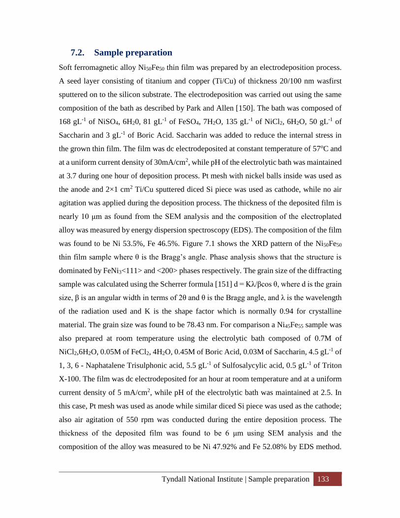
Tyndall National Institute | Sample preparation 133
7.2. Sample preparation
Soft ferromagnetic alloy Ni50Fe50 thin film was prepared by an electrodeposition process.
A seed layer consisting of titanium and copper (Ti/Cu) of thickness 20/100 nm wasfirst
sputtered on to the silicon substrate. The electrodeposition was carried out using the same
composition of the bath as described by Park and Allen [150]. The bath was composed of
168 gL-1 of NiSO4, 6H20, 81 gL-1 of FeSO4, 7H2O, 135 gL-1 of NiCl2, 6H2O, 50 gL-1 of
Saccharin and 3 gL-1 of Boric Acid. Saccharin was added to reduce the internal stress in
the grown thin film. The film was dc electrodeposited at constant temperature of 57oC and
at a uniform current density of 30mA/cm2, while pH of the electrolytic bath was maintained
at 3.7 during one hour of deposition process. Pt mesh with nickel balls inside was used as
the anode and 2×1 cm2 Ti/Cu sputtered diced Si piece was used as cathode, while no air
agitation was applied during the deposition process. The thickness of the deposited film is
nearly 10 μm as found from the SEM analysis and the composition of the electroplated
alloy was measured by energy dispersion spectroscopy (EDS). The composition of the film
was found to be Ni 53.5%, Fe 46.5%. Figure 7.1 shows the XRD pattern of the Ni50Fe50
thin film sample where θ is the Bragg’s angle. Phase analysis shows that the structure is
dominated by FeNi3<111> and <200> phases respectively. The grain size of the diffracting
sample was calculated using the Scherrer formula [151] d = Kλ/βcos θ, where d is the grain
size, β is an angular width in terms of 2θ and θ is the Bragg angle, and λ is the wavelength
of the radiation used and K is the shape factor which is normally 0.94 for crystalline
material. The grain size was found to be 78.43 nm. For comparison a Ni45Fe55 sample was
also prepared at room temperature using the electrolytic bath composed of 0.7M of
NiCl2,6H2O, 0.05M of FeCl2, 4H2O, 0.45M of Boric Acid, 0.03M of Saccharin, 4.5 gL-1 of
1, 3, 6 - Naphatalene Trisulphonic acid, 5.5 gL-1 of Sulfosalycylic acid, 0.5 gL-1 of Triton
X-100. The film was dc electrodeposited for an hour at room temperature and at a uniform
current density of 5 mA/cm2, while pH of the electrolytic bath was maintained at 2.5. In
this case, Pt mesh was used as anode while similar diced Si piece was used as the cathode;
also air agitation of 550 rpm was conducted during the entire deposition process. The
thickness of the deposited film was found to be 6 μm using SEM analysis and the
composition of the alloy was measured to be Ni 47.92% and Fe 52.08% by EDS method.
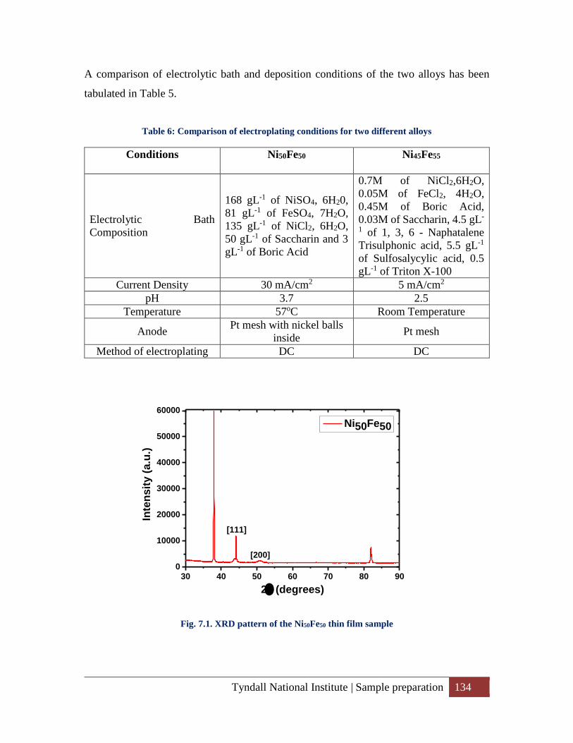
Tyndall National Institute | Sample preparation 134
A comparison of electrolytic bath and deposition conditions of the two alloys has been
tabulated in Table 5.
Table 6: Comparison of electroplating conditions for two different alloys
Conditions Ni50Fe50 Ni45Fe55
Electrolytic Bath
Composition
168 gL-1 of NiSO4, 6H20,
81 gL-1 of FeSO4, 7H2O,
135 gL-1 of NiCl2, 6H2O,
50 gL-1 of Saccharin and 3
gL-1 of Boric Acid
0.7M of NiCl2,6H2O,
0.05M of FeCl2, 4H2O,
0.45M of Boric Acid,
0.03M of Saccharin, 4.5 gL-
1 of 1, 3, 6 - Naphatalene
Trisulphonic acid, 5.5 gL-1
of Sulfosalycylic acid, 0.5
gL-1 of Triton X-100
Current Density 30 mA/cm2 5 mA/cm2
pH 3.7 2.5
Temperature 57oC Room Temperature
Anode Pt mesh with nickel balls
inside Pt mesh
Method of electroplating DC DC
30 40 50 60 70 80 900
10000
20000
30000
40000
50000
60000
Inte
nsit
y (
a.u
.)
2 (degrees)
Ni50Fe50
[111]
[200]
Fig. 7.1. XRD pattern of the Ni50Fe50 thin film sample
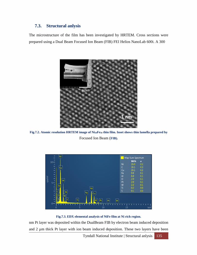
Tyndall National Institute | Structural anlysis 135
7.3. Structural anlysis
The microstructure of the film has been investigated by HRTEM. Cross sections were
prepared using a Dual Beam Focused Ion Beam (FIB) FEI Helios NanoLab 600i. A 300
Fig.7.2. Atomic resolution HRTEM image of Ni50Fe50 thin film. Inset shows thin lamella prepared by
Focused Ion Beam (FIB).
Fig.7.3. EDX elemental analysis of NiFe film at Ni rich region.
nm Pt layer was deposited within the DualBeam FIB by electron beam induced deposition
and 2 µm thick Pt layer with ion beam induced deposition. These two layers have been
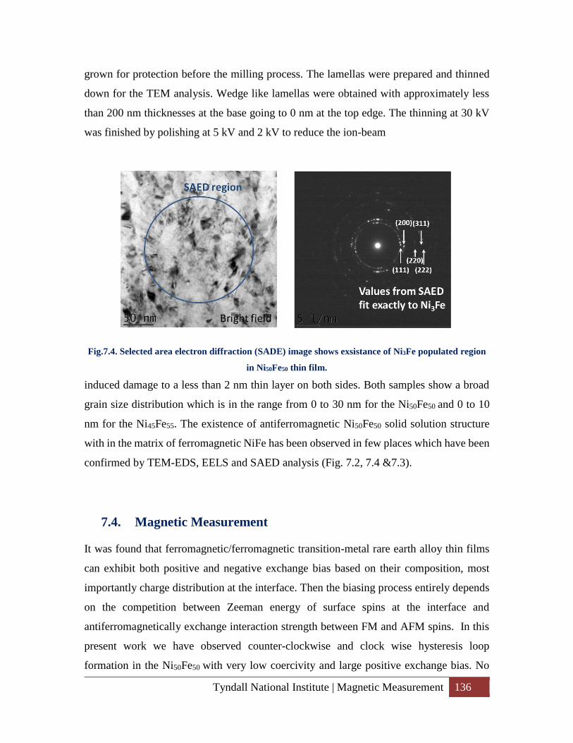
Tyndall National Institute | Magnetic Measurement 136
grown for protection before the milling process. The lamellas were prepared and thinned
down for the TEM analysis. Wedge like lamellas were obtained with approximately less
than 200 nm thicknesses at the base going to 0 nm at the top edge. The thinning at 30 kV
was finished by polishing at 5 kV and 2 kV to reduce the ion-beam
Fig.7.4. Selected area electron diffraction (SADE) image shows exsistance of Ni3Fe populated region
in Ni50Fe50 thin film.
induced damage to a less than 2 nm thin layer on both sides. Both samples show a broad
grain size distribution which is in the range from 0 to 30 nm for the Ni50Fe50 and 0 to 10
nm for the Ni45Fe55. The existence of antiferromagnetic Ni50Fe50 solid solution structure
with in the matrix of ferromagnetic NiFe has been observed in few places which have been
confirmed by TEM-EDS, EELS and SAED analysis (Fig. 7.2, 7.4 &7.3).
7.4. Magnetic Measurement
It was found that ferromagnetic/ferromagnetic transition-metal rare earth alloy thin films
can exhibit both positive and negative exchange bias based on their composition, most
importantly charge distribution at the interface. Then the biasing process entirely depends
on the competition between Zeeman energy of surface spins at the interface and
antiferromagnetically exchange interaction strength between FM and AFM spins. In this
present work we have observed counter-clockwise and clock wise hysteresis loop
formation in the Ni50Fe50 with very low coercivity and large positive exchange bias. No
Tyndall National Institute | Magnetic Measurement 137
exchange bias or inverse hysteresis loop was found in Ni45Fe55. These two opposite
(counter-clockwise/clockwise) hysteresis loop formation in Ni50Fe50 thin film depends
upon the field range of hysteresis loop measurement. Like most of the positive exchange
bias system Ni50Fe50also shows positive exchange bias shift at field direction when the loop
tracing field range is small (just above the saturation field) and the loop is also counter-
clockwise. When the film is measured with a higher loop tracing field range, it was
observed that the hysteresis loop follows reverse path with no exchange bias. We found
that the origin of this interesting phenomenon of dual type of hysteresis loop (counter-
clockwise/clockwise) observation with different field range hysteresis loop measurement
protocol depends on the microstructure of Ni50Fe50. To investigate the origin of this unique
and interesting phenomenon we have performed a detail microstructure and composition
analysis. The Ni,Fe solution behaves like admixture of antiferromagnetic (AFM) phase and
Ni50Fe50 naturally acts as ferromagnetic (FM). At low field range measurement the
interface behaves like typical FM-AFM interface and permits positive exchange bias. This
AFM coupling at interface can be overcome with a large field and AFM spins can be
aligned like FM spin. Thus the AFM-FM system behaves like FM at high field where all
spins are aligned at field direction.
Typical hysteresis loops of NiFe thin film after field cooled (FC) from 350K to room
temperature (300K) and low temperature 5K are shown in Fig. 7.5. A bias field of 1000 Oe
was applied and it shows positive exchange bias in NiFe system. ±200 Oe field range was
used to measured full hysteresis. When the same protocol was followed but with a different
field range of ±50,000 Oe a completely different result was observed. Normally a hysteresis
loop measurement shows an anti-clock wise MH loop, let call it as counter-clockwise
hysteresis. When we measured the same sample after FC with higher field range the MH
loop follows a clock wise path (Fig. 7.6-a). Both coercive field (HC) and remanence
magnetization (MR) are obtained reverse directions. Throughout the discussion we will call
it negative hysteresis. No step hysteresis has been found in ±50,000 Oe field range (Fig.
7.6-b). Thus it is clear that the negative coersivity does not come from twisted hysteresis
[152]. The positive hysteresis loops measured after +5T and -5T FC at 5K lay exactly on
the right and left sides of inverse hysteresis loop (5K) respectively. A range of shaped
hysteresis loops with various fields range were measured right after field cooled (FC) with
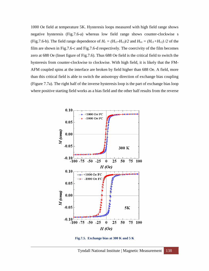
Tyndall National Institute | Magnetic Measurement 138
1000 Oe field at temperature 5K. Hysteresis loops measured with high field range shows
negative hysteresis (Fig.7.6-a) whereas low field range shows counter-clockwise s
(Fig.7.6-b). The field range dependence of Hc = (Hc1-Hc2)/2 and Hex = (Hc1+Hc2) /2 of the
film are shown in Fig.7.6-c and Fig.7.6-d respectively. The coercivity of the film becomes
zero at 688 Oe (Inset figure of Fig.7.6). Thus 688 Oe field is the critical field to switch the
hysteresis from counter-clockwise to clockwise. With high field, it is likely that the FM-
AFM coupled spins at the interface are broken by field higher than 688 Oe. A field, more
than this critical field is able to switch the anisotropy direction of exchange bias coupling
(Figure 7.7a). The right half of the inverse hysteresis loop is the part of exchange bias loop
where positive starting field works as a bias field and the other half results from the reverse
Fig.7.5. Exchange bias at 300 K and 5 K
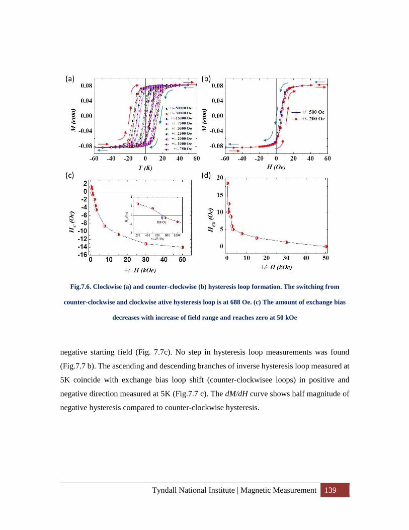
Tyndall National Institute | Magnetic Measurement 139
Fig.7.6. Clockwise (a) and counter-clockwise (b) hysteresis loop formation. The switching from
counter-clockwise and clockwise ative hysteresis loop is at 688 Oe. (c) The amount of exchange bias
decreases with increase of field range and reaches zero at 50 kOe
negative starting field (Fig. 7.7c). No step in hysteresis loop measurements was found
(Fig.7.7 b). The ascending and descending branches of inverse hysteresis loop measured at
5K coincide with exchange bias loop shift (counter-clockwisee loops) in positive and
negative direction measured at 5K (Fig.7.7 c). The dM/dH curve shows half magnitude of
negative hysteresis compared to counter-clockwise hysteresis.
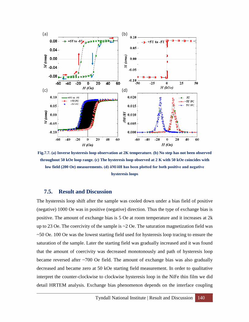
Tyndall National Institute | Result and Discussion 140
Fig.7.7. (a) Inverse hysteresis loop observation at 2K temperature. (b) No step has not been observed
throughout 50 kOe loop range. (c) The hysteresis loop observed at 2 K with 50 kOe coincides with
low field (200 Oe) measurements. (d) δM/δH has been plotted for both positive and negative
hysteresis loops
7.5. Result and Discussion
The hysteresis loop shift after the sample was cooled down under a bias field of positive
(negative) 1000 Oe was in positive (negative) direction. Thus the type of exchange bias is
positive. The amount of exchange bias is 5 Oe at room temperature and it increases at 2k
up to 23 Oe. The coercivity of the sample is ~2 Oe. The saturation magnetization field was
~50 Oe. 100 Oe was the lowest starting field used for hysteresis loop tracing to ensure the
saturation of the sample. Later the starting field was gradually increased and it was found
that the amount of coercivity was decreased monotonously and path of hysteresis loop
became reversed after ~700 Oe field. The amount of exchange bias was also gradually
decreased and became zero at 50 kOe starting field measurement. In order to qualitative
interpret the counter-clockwise to clockwise hysteresis loop in the NiFe thin film we did
detail HRTEM analysis. Exchange bias phenomenon depends on the interface coupling
Tyndall National Institute | Result and Discussion 141
between two different phases. The crystallographic relation between FM and AF phases
are identified in the film by structures mapped onto HRTEM image pattern. From precise
subnanoscale characterization and correlating these crystallographic structures with known
magnetic structures by neutron diffraction of similar material [152] as shown in Fig. 7.4 its
clear that in the matrix of ferromagnetic Ni50Fe50 there is tiny particles of Ni,Fe solid
solution which antiferromagnetic (AFM) in nature. It was observed that the amount of
exchange shift (HE) is much greater than the coercivity (HC) of the sample. From the detail
microstructural analysis with nanoscale resolution we ascertain that the Ni,Fe solid solution
is an admixture of AFM and FM phases and the interface to the Ni50Fe50 is effectively
provides a local exchange coupling which permits a positive exchange bias. This exchange
coupling at the interface can be developed and broken with large applied field. When a
positive high field (+50 kOe) is applied positive exchange coupling is generated at the
interface of the antiferromagnetic Ni3Fe and ferromagnetic Ni50Fe50. Hence first half of
hysteresis loop (descending branch) is generated in the positive quadrant and a high
negative field (-50 kOe) is applied at the end. This negative high field (-50 kOe) breaks the
exchange coupling and generates negative exchange bias coupling at the interface. While
measuring the second half of the hysteresis loop (ascending brunch) the curve follows
exchange shift loop path in negative field direction. Hence an inverse hysteresis loop is
generated. Negative coercivity has been earlier found in many multilayer thin film systems
due to helical or step like hysteresis loop formation. The sum of the magnitudes of
exchange shift in both directions (|+HEB|+|-HEB|) measured at 2K is equal to the coercivity
(HC) of the inverse hysteresis loop. The loop tracing range was gradually increased from ±
200 Oe to ± 50 kOe. The amount of exchange bias decreases and coercivity increases. Due
to the increase of gradual loop tracing field the exchange coupling generated at the interface
by bias field is broken by opposite high field in reverse direction. Hence the amount of
exchange bias and coercivity are decreased. After certain field the loop switches to other
direction and coercivity starts increasing. The Lowest exchange bias (0 Oe) and highest
coercivity is obtained with the loop tracing range of ±50 kOe.
Tyndall National Institute | Summary 142
7.6. Summary
In summary, we report that counter-clockwise and clockwise hysteresis loop formation
with very low coercivity and large positive exchange bias is observed in the Ni,Fe solid
solution. These two opposite (counter-clockwise to clockwise) hysteresis loop formation
depends upon the field range of hysteresis loop measurement. Ni50Fe50 thin film shows
positive exchange bias when the loop tracing field range is small (just above the saturation
field) and the loop is positive. If the film is measured with a higher range of loop tracing
field, a typical negative hysteresis loop with no exchange bias is observed. The origin of
this interesting phenomenon of dual type of hysteresis loop (positive and negative)
observation due to different range of field hysteresis loop measurement protocol depends
on the microstructure of Ni50Fe50. Admixture of antiferromagnetic NiFe and ferromagnetic
Ni50Fe50 acts like typical FM-AFM interface and permits positive exchange bias with very
low coersivity. This AFM coupling at interface can be overcome with the application of a
large field and AFM spins can be aligned like FM spin which leads to the formation of
negative hysteresis loop. Thus the AFM-FM system behaves like FM at high field where
all spins are aligned in the field direction.
Tyndall National Institute | Chapter - Conclusions 143
8. Chapter - Conclusions
In this work we have investigated different nanostructured magnetic materials which have
potential device applications. The main focus of the research was to investigate possibilities
of controlling and enhancing magnetic anisotropy by different nanostructures. We have
investigated the properties of samples through magnetic measurements and micromagnetic
simulation, playing particular attention to the shape and exchange anisotropy where a
particular type of nanostructure has huge influence on the hysteresis loop and magnetic
microstructure. A detail literature review was carried out to delineate the recent
development in the field. Various nanostructures such as lines, dots, anti-dots, etc. were
reported to control the anisotropy.
A new model to achieve controllable magnetic anisotropy through the formation of
magnetic dipoles in continuous ferromagnetic thin films due to a unique nanomodulation
has been discussed in the thesis. Experimental evidence of well-ordered dipoles with
metastable state has been detected by means of variation of magnetic anisotropy, step
hysteresis, and MFM imaging. The anisotropy model, based on collective dipolar
interaction, is used to demonstrate the ability to control anisotropy in continuous
ferromagnetic thin films by minimizing magnetostatic energy through nanomodulation.
The generalized model helps us to find out possible anisotropy based on material property
and geometrical arrangement of nanopattern. Additionally, the formation of a metastable
single domain resists vortex formation in nanopatterned ferromagnetic thin films, which
are essential for realizing devices, such as volatile memory, magnetically frustrated
patterned media, highly integrated nanoscale magnetic devices, etc.
If the patterned frequency is comparable to the frequency of magnetic wave then one can
assume the effect of pattern on the propagation of magnetic wave. The frequency of any
wave is inversely proportional to the wavelength.
The frequency of a wave in free space can be written as
But for a magnetic material this is written as
Cf2
00f
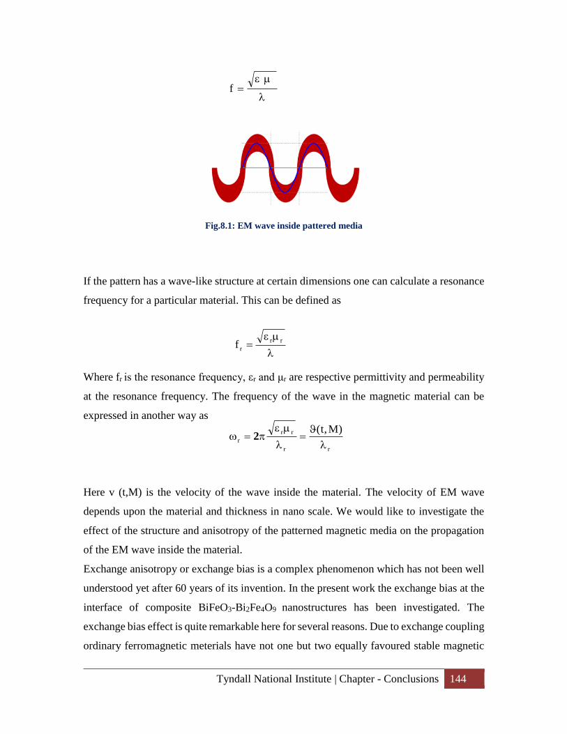
Tyndall National Institute | Chapter - Conclusions 144
Fig.8.1: EM wave inside pattered media
If the pattern has a wave-like structure at certain dimensions one can calculate a resonance
frequency for a particular material. This can be defined as
Where fr is the resonance frequency, εr and μr are respective permittivity and permeability
at the resonance frequency. The frequency of the wave in the magnetic material can be
expressed in another way as
Here v (t,M) is the velocity of the wave inside the material. The velocity of EM wave
depends upon the material and thickness in nano scale. We would like to investigate the
effect of the structure and anisotropy of the patterned magnetic media on the propagation
of the EM wave inside the material.
Exchange anisotropy or exchange bias is a complex phenomenon which has not been well
understood yet after 60 years of its invention. In the present work the exchange bias at the
interface of composite BiFeO3-Bi2Fe4O9 nanostructures has been investigated. The
exchange bias effect is quite remarkable here for several reasons. Due to exchange coupling
ordinary ferromagnetic meterials have not one but two equally favoured stable magnetic
f
rr
rf
rr
rr
r
)M,t(
2
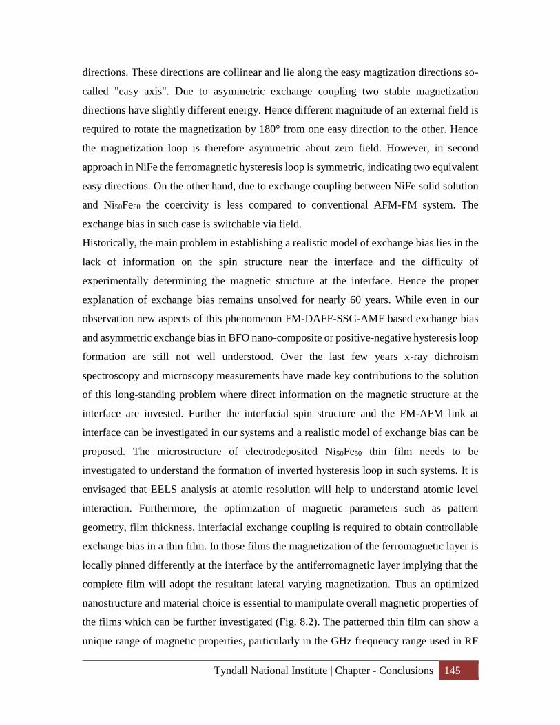
Tyndall National Institute | Chapter - Conclusions 145
directions. These directions are collinear and lie along the easy magtization directions so-
called "easy axis". Due to asymmetric exchange coupling two stable magnetization
directions have slightly different energy. Hence different magnitude of an external field is
required to rotate the magnetization by 180° from one easy direction to the other. Hence
the magnetization loop is therefore asymmetric about zero field. However, in second
approach in NiFe the ferromagnetic hysteresis loop is symmetric, indicating two equivalent
easy directions. On the other hand, due to exchange coupling between NiFe solid solution
and Ni50Fe50 the coercivity is less compared to conventional AFM-FM system. The
exchange bias in such case is switchable via field.
Historically, the main problem in establishing a realistic model of exchange bias lies in the
lack of information on the spin structure near the interface and the difficulty of
experimentally determining the magnetic structure at the interface. Hence the proper
explanation of exchange bias remains unsolved for nearly 60 years. While even in our
observation new aspects of this phenomenon FM-DAFF-SSG-AMF based exchange bias
and asymmetric exchange bias in BFO nano-composite or positive-negative hysteresis loop
formation are still not well understood. Over the last few years x-ray dichroism
spectroscopy and microscopy measurements have made key contributions to the solution
of this long-standing problem where direct information on the magnetic structure at the
interface are invested. Further the interfacial spin structure and the FM-AFM link at
interface can be investigated in our systems and a realistic model of exchange bias can be
proposed. The microstructure of electrodeposited Ni50Fe50 thin film needs to be
investigated to understand the formation of inverted hysteresis loop in such systems. It is
envisaged that EELS analysis at atomic resolution will help to understand atomic level
interaction. Furthermore, the optimization of magnetic parameters such as pattern
geometry, film thickness, interfacial exchange coupling is required to obtain controllable
exchange bias in a thin film. In those films the magnetization of the ferromagnetic layer is
locally pinned differently at the interface by the antiferromagnetic layer implying that the
complete film will adopt the resultant lateral varying magnetization. Thus an optimized
nanostructure and material choice is essential to manipulate overall magnetic properties of
the films which can be further investigated (Fig. 8.2). The patterned thin film can show a
unique range of magnetic properties, particularly in the GHz frequency range used in RF
Tyndall National Institute | Chapter - Conclusions 146
communications. If the patterned frequency is comparable to the frequency of magnetic
wave then one can assume the effect of pattern on the propagation of magnetic wave.
Fig.8.2. Single and multilayer nanomodulated film
The impact of this work will be reflected on size reduction of magnetic components with
better performance for miniaturized ICT devices and development of cost effective process.
We have chosen modulated PR electrodeposition/ dc-rf-sputtering combined with
nanoimprint lithography, a novel approach, for sample preparation. We believe that the
work will result in novel nanomodulaed/multilater thin film of composite material, which
would delineate novel physical insights in the new magnetic ‘multi- nano- layer-structures’
with a technological impact in ICT industry. The principal significance of this work will
stem from the cost effective and compatible manufacturing process for the next generation
high frequency micromagnetic devices for various applications e.g. telecommunication
industry, storage media, magnetic component based electronics, etc.
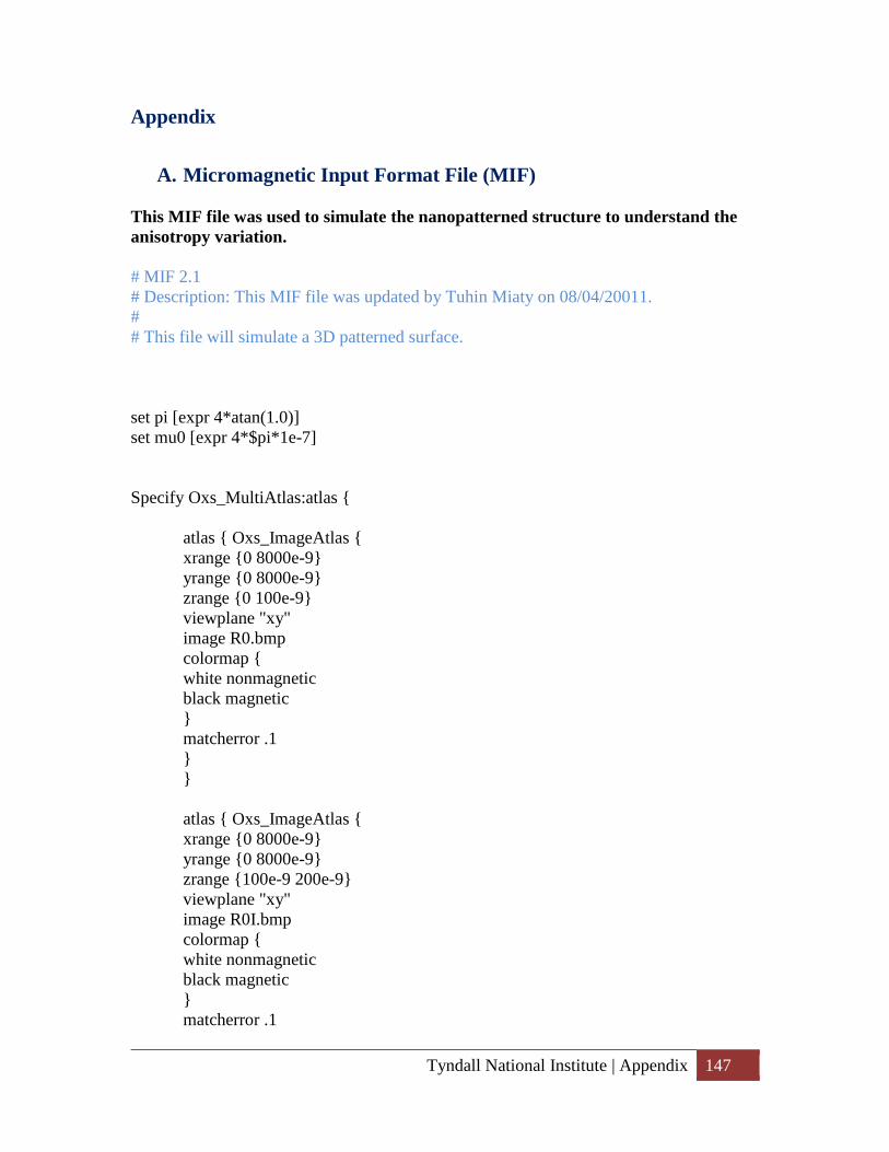
Tyndall National Institute | Appendix 147
Appendix
A. Micromagnetic Input Format File (MIF)
This MIF file was used to simulate the nanopatterned structure to understand the
anisotropy variation.
# MIF 2.1
# Description: This MIF file was updated by Tuhin Miaty on 08/04/20011.
#
# This file will simulate a 3D patterned surface.
set pi [expr 4*atan(1.0)]
set mu0 [expr 4*$pi*1e-7]
Specify Oxs_MultiAtlas:atlas
atlas Oxs_ImageAtlas
xrange 0 8000e-9
yrange 0 8000e-9
zrange 0 100e-9
viewplane "xy"
image R0.bmp
colormap
white nonmagnetic
black magnetic
matcherror .1
atlas Oxs_ImageAtlas
xrange 0 8000e-9
yrange 0 8000e-9
zrange 100e-9 200e-9
viewplane "xy"
image R0I.bmp
colormap
white nonmagnetic
black magnetic
matcherror .1
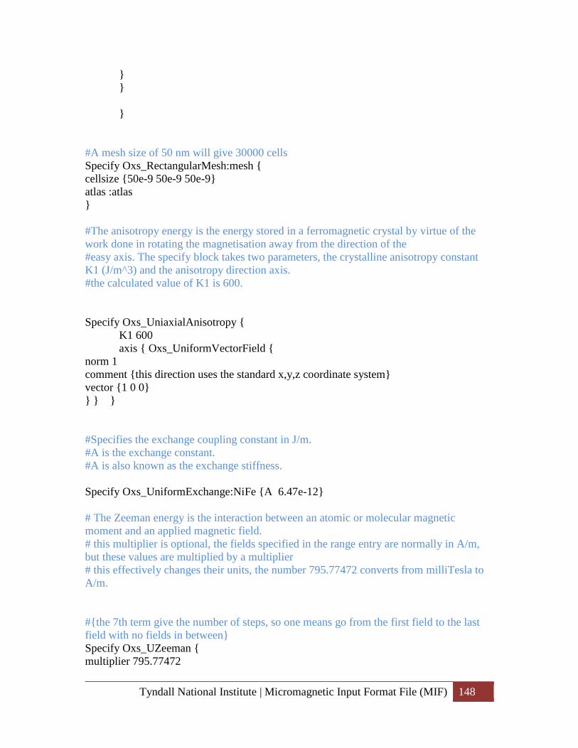
Tyndall National Institute | Micromagnetic Input Format File (MIF) 148
#A mesh size of 50 nm will give 30000 cells
Specify Oxs_RectangularMesh:mesh
cellsize 50e-9 50e-9 50e-9
atlas :atlas
#The anisotropy energy is the energy stored in a ferromagnetic crystal by virtue of the
work done in rotating the magnetisation away from the direction of the
#easy axis. The specify block takes two parameters, the crystalline anisotropy constant
K1 (J/m^3) and the anisotropy direction axis.
#the calculated value of K1 is 600.
Specify Oxs_UniaxialAnisotropy
K1 600
axis Oxs_UniformVectorField
norm 1
comment this direction uses the standard x,y,z coordinate system
vector 1 0 0
#Specifies the exchange coupling constant in J/m.
#A is the exchange constant.
#A is also known as the exchange stiffness.
Specify Oxs_UniformExchange:NiFe A 6.47e-12
# The Zeeman energy is the interaction between an atomic or molecular magnetic
moment and an applied magnetic field.
# this multiplier is optional, the fields specified in the range entry are normally in A/m,
but these values are multiplied by a multiplier
# this effectively changes their units, the number 795.77472 converts from milliTesla to
A/m.
#the 7th term give the number of steps, so one means go from the first field to the last
field with no fields in between
Specify Oxs_UZeeman
multiplier 795.77472

Tyndall National Institute | Micromagnetic Input Format File (MIF) 149
Hrange
0 0 0 400 0 0 10
# this is a standard specify term which is put into every mif file. It is built on the
assumption that the demagnetisation field is constant in each cell and computers the
average
# demagnetisation field through the cell.
Specify Oxs_Demag
# Minimisation evolver.
Specify Oxs_CGEvolve
Specify Oxs_MinDriver
evolver Oxs_CGEvolve
mesh :mesh
comment this value is in A/m, the oommf manual says that it is usually not possible to
obtain a value of mxHxm below about 0.01
stopping_mxHxm 1
Ms
Oxs_AtlasScalarField
atlas :atlas
default_value 0
values
nonmagnetic 0
magnetic 1.2e6
comment mo gives the initial configuration of the magnetisation unit spins
m0 0.017452406437283376 0.99984769515639127 0.0
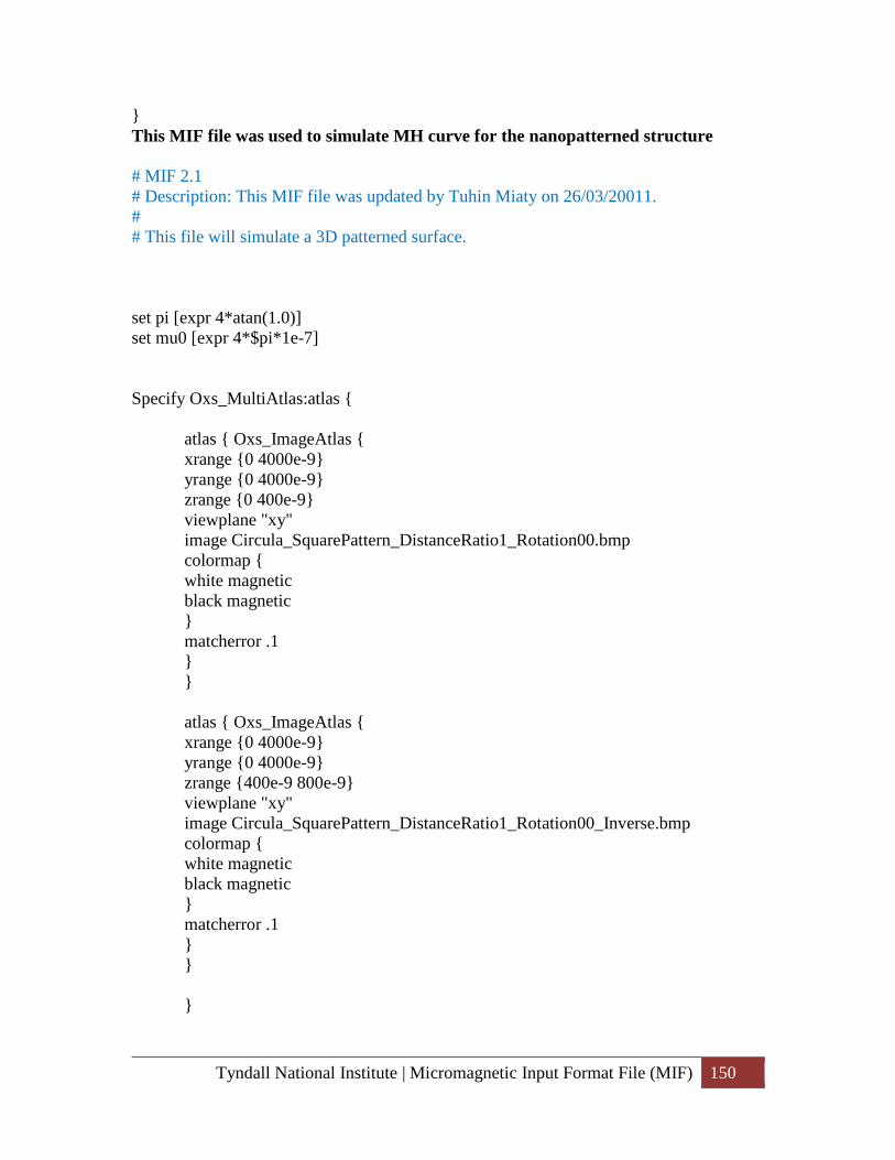
Tyndall National Institute | Micromagnetic Input Format File (MIF) 150
This MIF file was used to simulate MH curve for the nanopatterned structure
# MIF 2.1
# Description: This MIF file was updated by Tuhin Miaty on 26/03/20011.
#
# This file will simulate a 3D patterned surface.
set pi [expr 4*atan(1.0)]
set mu0 [expr 4*$pi*1e-7]
Specify Oxs_MultiAtlas:atlas
atlas Oxs_ImageAtlas
xrange 0 4000e-9
yrange 0 4000e-9
zrange 0 400e-9
viewplane "xy"
image Circula_SquarePattern_DistanceRatio1_Rotation00.bmp
colormap
white magnetic
black magnetic
matcherror .1
atlas Oxs_ImageAtlas
xrange 0 4000e-9
yrange 0 4000e-9
zrange 400e-9 800e-9
viewplane "xy"
image Circula_SquarePattern_DistanceRatio1_Rotation00_Inverse.bmp
colormap
white magnetic
black magnetic
matcherror .1

Tyndall National Institute | Micromagnetic Input Format File (MIF) 151
#A mesh size of 50 nm will give 30000 cells
Specify Oxs_RectangularMesh:mesh
cellsize 50e-9 50e-9 50e-9
atlas :atlas
#The anisotropy energy is the energy stored in a ferromagnetic crystal by virtue of the
work done in rotating the magnetisation away from the direction of the
#easy axis. The specify block takes two parameters, the crystalline anisotropy constant
K1 (J/m^3) and the anisotropy direction axis.
#the calculated value of K1 is 600.
Specify Oxs_UniaxialAnisotropy
K1 600
axis Oxs_UniformVectorField
norm 1
comment this direction uses the standard x,y,z coordinate system
vector 1 0 0
#Specifies the exchange coupling constant in J/m.
#A is the exchange constant.
#A is also known as the exchange stiffness.
Specify Oxs_UniformExchange:NiFe A 6.47e-12
# The Zeeman energy is the interaction between an atomic or molecular magnetic
moment and an applied magnetic field.
# this multiplier is optional, the fields specified in the range entry are normally in A/m,
but these values are multiplied by a multiplier
# this effectively changes their units, the number 795.77472 converts from milliTesla to
A/m.
#the 7th term give the number of steps, so one means go from the first field to the last
field with no fields in between
Specify Oxs_UZeeman
multiplier 795.77472
Hrange
1000 0 0 0 0 0 100
0 0 0 -1000 0 0 100
-1000 0 0 0 0 0 100
Tyndall National Institute | Micromagnetic Input Format File (MIF) 152
0 0 0 1000 0 0 100
# this is a standard specify term which is put into every mif file. It is built on the
assumption that the demagnetisation field is constant in each cell and computers the
average
# demagnetisation field through the cell.
Specify Oxs_Demag
# Minimisation evolver.
Specify Oxs_CGEvolve
Specify Oxs_MinDriver
evolver Oxs_CGEvolve
mesh :mesh
comment this value is in A/m, the oommf manual says that it is usually not possible to
obtain a value of mxHxm below about 0.01
stopping_mxHxm 1
Ms
Oxs_AtlasScalarField
atlas :atlas
default_value 0
values
magnetic 1.2e6
comment mo gives the initial configuration of the magnetisation unit spins
m0 0.017452406437283376 0.99984769515639127 0.0
Tyndall National Institute | Example of sequence file used for SQUID
magnetic measurement
153
B. Example of sequence file used for SQUID magnetic measurement
MT & MH measurement
Set Cal Factor: Temp: Tolerance 0.050
Set Temperature 350.000K at 10.000K/min.
Waitfor Temp:Stable Delay:1secs
Run Sequence: C:\SQUID_DATA\Tuhin\Sequence\Tyndall\Ashish\Demag.seq
Set Magnetic Field 50000.00 Oe, Oscillate, Hi Res Enabled
Waitfor Field:Stable Delay:1secs
Set Temperature 2.000K at 10.000K/min.
Set Datafile: [**INVALID PATH**]
C:\SQUID_DATA\Tuhin\Data\CGCRI\BFO_B\2013_New\BFO_B_Positive_5T_MH_2
K_20130206
Run Sequence:
C:\SQUID_DATA\Tuhin\Sequence\Tyndall\CGCRI\BFO\MH_5T_Positive.seq
Set Magnetic Field 0.00 Oe, No Overshoot, Hi Res Enabled
Waitfor Field:Stable Delay:1secs
Set Temperature 350.000K at 10.000K/min.
Waitfor Temp:Stable Delay:1secs
Run Sequence: C:\SQUID_DATA\Tuhin\Sequence\Tyndall\Demag.seq
Set Magnetic Field -50000.00 Oe, Oscillate, Hi Res Enabled
Waitfor Field:Stable Delay:1secs
Set Temperature 2.000K at 10.000K/min.
Set Datafile: [**INVALID PATH**]
C:\SQUID_DATA\Tuhin\Data\CGCRI\BFO_B\2013_New\BFO_B_Negaitive_5T_MH_
2K_20130206
Run Sequence:
C:\SQUID_DATA\Tuhin\Sequence\Tyndall\CGCRI\BFO\MH_5T_Positive.seq
Set Magnetic Field 0.00 Oe, Oscillate, Hi Res Enabled
Waitfor Field:Stable Delay:1secs
ZFC Sequence
Scan Temp from 2.000K to 99.00K at 1.000K/min in 1K increments (98 steps) Sweep
Measure DC: 4.00 cm, 28 pts, 2 scans, AutoRng, Long, Iterative Reg., track:No,
raw:Yes, diag:Yes
End Scan
Scan Temp from 100.0K to 350.0K at 2.500K/min in 2.5K increments (101 steps) Sweep
Measure DC: 4.00 cm, 28 pts, 2 scans, AutoRng, Long, Iterative Reg., track:No,
raw:Yes, diag:Yes
End Scan
AC ZFC sequence

Tyndall National Institute | Example of sequence file used for SQUID
magnetic measurement
154
Scan Temp from 5.000K to 350.0K at 2.500K/min in 2.5K increments (139 steps) Sweep
Measure AC: 2.0000 Oe, 99.947 Hz, 2 meas, 2 blks, 1E-005 Null, x 1, 1 s, AutoRng,
track:No, diag:Yes, raw:Yes
End Scan
FC Sequence
Scan Temp from 350.0K to 100.0K at 2.500K/min in -2.5K increments (101 steps) Sweep
Measure DC: 4.00 cm, 28 pts, 2 scans, AutoRng, Long, Iterative Reg., track:No,
raw:Yes, diag:Yes
End Scan
Scan Temp from 99.00K to 2.000K at 1.000K/min in -1K increments (98 steps) Sweep
Measure DC: 4.00 cm, 28 pts, 2 scans, AutoRng, Long, Iterative Reg., track:No,
raw:Yes, diag:Yes
End Scan
AC FC sequence
Scan Temp from 350.000K to 5.0K at 2.500K/min in 2.5K increments (139 steps) Sweep
Measure AC: 2.0000 Oe, 99.947 Hz, 2 meas, 2 blks, 1E-005 Null, x 1, 1 s, AutoRng,
track:No, diag:Yes, raw:Yes
End Scan
Positive MH curve Sequence
Scan Field from 50000.00Oe to 10000.00 Oe in -20000.00 Oe increments (3 steps), No
Overshoot, Hi Res Enabled
Measure DC: 4.00 cm, 28 pts, 2 scans, AutoRng, Long, Iterative Reg., track:No,
raw:Yes, diag:Yes
End Scan
Scan Field from 8000.00Oe to -2000.00 Oe in -2000.00 Oe increments (6 steps), No
Overshoot, Hi Res Enabled
Measure DC: 4.00 cm, 28 pts, 2 scans, AutoRng, Long, Iterative Reg., track:No,
raw:Yes, diag:Yes
End Scan
Scan Field from -2500.00Oe to -5000.00 Oe in -500.00 Oe increments (6 steps), No
Overshoot, Hi Res Enabled
Measure DC: 4.00 cm, 28 pts, 3 scans, AutoRng, Long, Iterative Reg., track:No,
raw:Yes, diag:Yes
End Scan
Scan Field from -6000.00Oe to -8000.00 Oe in -2000.00 Oe increments (2 steps), No
Overshoot, Hi Res Enabled
Measure DC: 4.00 cm, 28 pts, 2 scans, AutoRng, Long, Iterative Reg., track:No,
raw:Yes, diag:Yes
End Scan

Tyndall National Institute | Example of sequence file used for SQUID
magnetic measurement
155
Scan Field from -10000.00Oe to -50000.00 Oe in -20000.00 Oe increments (3 steps), No
Overshoot, Hi Res Enabled
Measure DC: 4.00 cm, 28 pts, 2 scans, AutoRng, Long, Iterative Reg., track:No,
raw:Yes, diag:Yes
End Scan
Scan Field from -30000.00Oe to -10000.00 Oe in 20000.00 Oe increments (2 steps), No
Overshoot, Hi Res Enabled
Measure DC: 4.00 cm, 28 pts, 2 scans, AutoRng, Long, Iterative Reg., track:No,
raw:Yes, diag:Yes
End Scan
Scan Field from -8000.00Oe to -4000.00 Oe in 2000.00 Oe increments (3 steps), No
Overshoot, Hi Res Enabled
Measure DC: 4.00 cm, 28 pts, 2 scans, AutoRng, Long, Iterative Reg., track:No,
raw:Yes, diag:Yes
End Scan
Scan Field from -3000.00Oe to 2000.00 Oe in 500.00 Oe increments (11 steps), No
Overshoot, Hi Res Enabled
Measure DC: 4.00 cm, 28 pts, 2 scans, AutoRng, Long, Iterative Reg., track:No,
raw:Yes, diag:Yes
End Scan
Scan Field from 3000.00Oe to 9000.00 Oe in 2000.00 Oe increments (4 steps), No
Overshoot, Hi Res Enabled
Measure DC: 4.00 cm, 28 pts, 2 scans, AutoRng, Long, Iterative Reg., track:No,
raw:Yes, diag:Yes
End Scan
Scan Field from 10000.00Oe to 50000.00 Oe in 20000.00 Oe increments (3 steps), No
Overshoot, Hi Res Enabled
Measure DC: 4.00 cm, 28 pts, 2 scans, AutoRng, Long, Iterative Reg., track:No,
raw:Yes, diag:Yes
End Scan
Negative MH curve sequence
Scan Field from -50000.00Oe to -10000.00 Oe in 20000.00 Oe increments (3 steps), No
Overshoot, Hi Res Enabled
Measure DC: 4.00 cm, 28 pts, 2 scans, AutoRng, Long, Iterative Reg., track:No,
raw:Yes, diag:Yes
End Scan
Scan Field from -8000.00Oe to -2000.00 Oe in 2000.00 Oe increments (4 steps), No
Overshoot, Hi Res Enabled
Measure DC: 4.00 cm, 28 pts, 2 scans, AutoRng, Long, Iterative Reg., track:No,
raw:Yes, diag:Yes
End Scan
Scan Field from -1000.00Oe to 1000.00 Oe in 500.00 Oe increments (5 steps), No
Overshoot, Hi Res Enabled
Tyndall National Institute | Example of sequence file used for SQUID
magnetic measurement
156
Measure DC: 4.00 cm, 28 pts, 2 scans, AutoRng, Long, Iterative Reg., track:No,
raw:Yes, diag:Yes
End Scan
Scan Field from 1500.00Oe to 5500.00 Oe in 500.00 Oe increments (9 steps), No
Overshoot, Hi Res Enabled
Measure DC: 4.00 cm, 28 pts, 2 scans, AutoRng, Long, Iterative Reg., track:No,
raw:Yes, diag:Yes
End Scan
Scan Field from 6000.00Oe to 8000.00 Oe in 2000.00 Oe increments (2 steps), No
Overshoot, Hi Res Enabled
Measure DC: 4.00 cm, 28 pts, 2 scans, AutoRng, Long, Iterative Reg., track:No,
raw:Yes, diag:Yes
End Scan
Scan Field from 10000.00Oe to 50000.00 Oe in 20000.00 Oe increments (3 steps), No
Overshoot, Hi Res Enabled
Measure DC: 4.00 cm, 28 pts, 2 scans, AutoRng, Long, Iterative Reg., track:No,
raw:Yes, diag:Yes
End Scan
Scan Field from 30000.00Oe to 10000.00 Oe in -20000.00 Oe increments (2 steps), No
Overshoot, Hi Res Enabled
Measure DC: 4.00 cm, 28 pts, 2 scans, AutoRng, Long, Iterative Reg., track:No,
raw:Yes, diag:Yes
End Scan
Scan Field from 8000.00Oe to 4000.00 Oe in -2000.00 Oe increments (3 steps), No
Overshoot, Hi Res Enabled
Measure DC: 4.00 cm, 28 pts, 2 scans, AutoRng, Long, Iterative Reg., track:No,
raw:Yes, diag:Yes
End Scan
Scan Field from 3000.00Oe to -1000.00 Oe in -500.00 Oe increments (9 steps), No
Overshoot, Hi Res Enabled
Measure DC: 4.00 cm, 28 pts, 2 scans, AutoRng, Long, Iterative Reg., track:No,
raw:Yes, diag:Yes
End Scan
Scan Field from -1500.00Oe to -4000.00 Oe in -500.00 Oe increments (6 steps), No
Overshoot, Hi Res Enabled
Measure DC: 4.00 cm, 28 pts, 2 scans, AutoRng, Long, Iterative Reg., track:No,
raw:Yes, diag:Yes
End Scan
Scan Field from -5000.00Oe to -9000.00 Oe in -2000.00 Oe increments (3 steps), No
Overshoot, Hi Res Enabled
Measure DC: 4.00 cm, 28 pts, 2 scans, AutoRng, Long, Iterative Reg., track:No,
raw:Yes, diag:Yes
End Scan
Scan Field from -10000.00Oe to -50000.00 Oe in -20000.00 Oe increments (3 steps), No
Overshoot, Hi Res Enabled
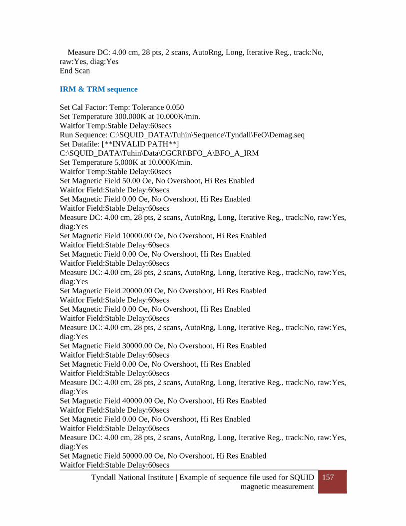
Tyndall National Institute | Example of sequence file used for SQUID
magnetic measurement
157
Measure DC: 4.00 cm, 28 pts, 2 scans, AutoRng, Long, Iterative Reg., track:No,
raw:Yes, diag:Yes
End Scan
IRM & TRM sequence
Set Cal Factor: Temp: Tolerance 0.050
Set Temperature 300.000K at 10.000K/min.
Waitfor Temp:Stable Delay:60secs
Run Sequence: C:\SQUID_DATA\Tuhin\Sequence\Tyndall\FeO\Demag.seq
Set Datafile: [**INVALID PATH**]
C:\SQUID_DATA\Tuhin\Data\CGCRI\BFO_A\BFO_A_IRM
Set Temperature 5.000K at 10.000K/min.
Waitfor Temp:Stable Delay:60secs
Set Magnetic Field 50.00 Oe, No Overshoot, Hi Res Enabled
Waitfor Field:Stable Delay:60secs
Set Magnetic Field 0.00 Oe, No Overshoot, Hi Res Enabled
Waitfor Field:Stable Delay:60secs
Measure DC: 4.00 cm, 28 pts, 2 scans, AutoRng, Long, Iterative Reg., track:No, raw:Yes,
diag:Yes
Set Magnetic Field 10000.00 Oe, No Overshoot, Hi Res Enabled
Waitfor Field:Stable Delay:60secs
Set Magnetic Field 0.00 Oe, No Overshoot, Hi Res Enabled
Waitfor Field:Stable Delay:60secs
Measure DC: 4.00 cm, 28 pts, 2 scans, AutoRng, Long, Iterative Reg., track:No, raw:Yes,
diag:Yes
Set Magnetic Field 20000.00 Oe, No Overshoot, Hi Res Enabled
Waitfor Field:Stable Delay:60secs
Set Magnetic Field 0.00 Oe, No Overshoot, Hi Res Enabled
Waitfor Field:Stable Delay:60secs
Measure DC: 4.00 cm, 28 pts, 2 scans, AutoRng, Long, Iterative Reg., track:No, raw:Yes,
diag:Yes
Set Magnetic Field 30000.00 Oe, No Overshoot, Hi Res Enabled
Waitfor Field:Stable Delay:60secs
Set Magnetic Field 0.00 Oe, No Overshoot, Hi Res Enabled
Waitfor Field:Stable Delay:60secs
Measure DC: 4.00 cm, 28 pts, 2 scans, AutoRng, Long, Iterative Reg., track:No, raw:Yes,
diag:Yes
Set Magnetic Field 40000.00 Oe, No Overshoot, Hi Res Enabled
Waitfor Field:Stable Delay:60secs
Set Magnetic Field 0.00 Oe, No Overshoot, Hi Res Enabled
Waitfor Field:Stable Delay:60secs
Measure DC: 4.00 cm, 28 pts, 2 scans, AutoRng, Long, Iterative Reg., track:No, raw:Yes,
diag:Yes
Set Magnetic Field 50000.00 Oe, No Overshoot, Hi Res Enabled
Waitfor Field:Stable Delay:60secs

Tyndall National Institute | Example of sequence file used for SQUID
magnetic measurement
158
Set Magnetic Field 0.00 Oe, No Overshoot, Hi Res Enabled
Waitfor Field:Stable Delay:60secs
Measure DC: 4.00 cm, 28 pts, 2 scans, AutoRng, Long, Iterative Reg., track:No, raw:Yes,
diag:Yes
Set Temperature 300.000K at 10.000K/min.
Waitfor Temp:Stable Delay:60secs
Run Sequence: C:\SQUID_DATA\Tuhin\Sequence\Tyndall\FeO\Demag.seq
Set Datafile: [**INVALID PATH**]
C:\SQUID_DATA\Tuhin\Data\CGCRI\BFO_A\BFO_A_TRM
Set Magnetic Field 50000.00 Oe, No Overshoot, Hi Res Enabled
Waitfor Field:Stable Delay:60secs
Set Temperature 5.000K at 10.000K/min.
Waitfor Temp:Stable Delay:60secs
Set Magnetic Field 0.00 Oe, No Overshoot, Hi Res Enabled
Waitfor Field:Stable Delay:60secs
Measure DC: 4.00 cm, 28 pts, 2 scans, AutoRng, Long, Iterative Reg., track:No, raw:Yes,
diag:Yes
Set Temperature 300.000K at 10.000K/min.
Waitfor Temp:Stable Delay:60secs
Run Sequence: C:\SQUID_DATA\Tuhin\Sequence\Tyndall\FeO\Demag.seq
Set Magnetic Field 40000.00 Oe, No Overshoot, Hi Res Enabled
Waitfor Field:Stable Delay:60secs
Set Temperature 5.000K at 10.000K/min.
Waitfor Temp:Stable Delay:60secs
Set Magnetic Field 0.00 Oe, No Overshoot, Hi Res Enabled
Waitfor Field:Stable Delay:60secs
Measure DC: 4.00 cm, 28 pts, 2 scans, AutoRng, Long, Iterative Reg., track:No, raw:Yes,
diag:Yes
Set Temperature 300.000K at 10.000K/min.
Waitfor Temp:Stable Delay:60secs
Run Sequence: C:\SQUID_DATA\Tuhin\Sequence\Tyndall\FeO\Demag.seq
Set Magnetic Field 30000.00 Oe, No Overshoot, Hi Res Enabled
Waitfor Field:Stable Delay:60secs
Set Temperature 5.000K at 10.000K/min.
Waitfor Temp:Stable Delay:60secs
Set Magnetic Field 0.00 Oe, No Overshoot, Hi Res Enabled
Waitfor Field:Stable Delay:60secs
Measure DC: 4.00 cm, 28 pts, 2 scans, AutoRng, Long, Iterative Reg., track:No, raw:Yes,
diag:Yes
Set Temperature 300.000K at 10.000K/min.
Waitfor Temp:Stable Delay:60secs
Run Sequence: C:\SQUID_DATA\Tuhin\Sequence\Tyndall\FeO\Demag.seq
Set Magnetic Field 20000.00 Oe, No Overshoot, Hi Res Enabled
Waitfor Field:Stable Delay:60secs
Set Temperature 5.000K at 10.000K/min.
Waitfor Temp:Stable Delay:60secs

Tyndall National Institute | Example of sequence file used for SQUID
magnetic measurement
159
Set Magnetic Field 0.00 Oe, No Overshoot, Hi Res Enabled
Waitfor Field:Stable Delay:60secs
Measure DC: 4.00 cm, 28 pts, 2 scans, AutoRng, Long, Iterative Reg., track:No, raw:No,
diag:Yes
Set Temperature 300.000K at 10.000K/min.
Waitfor Temp:Stable Delay:60secs
Run Sequence: C:\SQUID_DATA\Tuhin\Sequence\Tyndall\FeO\Demag.seq
Set Magnetic Field 10000.00 Oe, No Overshoot, Hi Res Enabled
Waitfor Field:Stable Delay:60secs
Set Temperature 5.000K at 10.000K/min.
Waitfor Temp:Stable Delay:60secs
Set Magnetic Field 0.00 Oe, No Overshoot, Hi Res Enabled
Waitfor Field:Stable Delay:60secs
Measure DC: 4.00 cm, 28 pts, 2 scans, AutoRng, Long, Iterative Reg., track:No, raw:Yes,
diag:Yes
Set Temperature 300.000K at 10.000K/min.
Waitfor Temp:Stable Delay:60secs
Run Sequence: C:\SQUID_DATA\Tuhin\Sequence\Tyndall\FeO\Demag.seq
Set Magnetic Field 50.00 Oe, No Overshoot, Hi Res Enabled
Waitfor Field:Stable Delay:60secs
Set Temperature 5.000K at 10.000K/min.
Waitfor Temp:Stable Delay:60secs
Set Magnetic Field 0.00 Oe, No Overshoot, Hi Res Enabled
Waitfor Field:Stable Delay:60secs
Measure DC: 4.00 cm, 28 pts, 2 scans, AutoRng, Long, Iterative Reg., track:No, raw:Yes,
diag:Yes
Set Temperature 2.000K at 10.000K/min.
Waitfor Temp:Stable Delay:60secs
Set Magnetic Field 0.00 Oe, No Overshoot, Hi Res Enabled
Waitfor Field:Stable Delay:60secs
Tyndall National Institute | Bibliography: 160
Bibliography:
1. Richard J. Harrison1 and Joshua M. Feinberg (ElEmEnts, Vol. 5, pp. 209–215,
2009)
2. Introduction to the theory of Ferromagnetism. Oxford Science Publications, 2nd
edition (2000)
3. J. Briones, F. Montaigne, D. Lacour, G. Lengaigne, S. Girod, and M. Hehn, Appl.
Phys. Express, vol.3, pp.073002, 2010.
4. O'Handley RC.:Modern Magnetic Materials: Principles and Applications. John
Wiley and Sons, Inc. (1999).
5. S. P. Li, D. Peyrade, M. Natali, A. Lebib, Y. Chen, U. Ebels, L. D. Buda, and K.
Ounadjela, Phys. Rev. Lett. 86, 1102 (2001).
6. R. P. Cowburn, D. K. Koltsov, A. O. Adeyeye, M. E. Welland, and D. M. Tricker,
Phys. Rev. Lett. 83, 1042 (1999).
7. S. P. Li, Jeffrey F. Godsell, and Saibal Roy, Journal of Applied Physics 108, 093915
(2010)
8. C. Chappert, H. Bernas, J. Ferre, V. Kottler, J. P. Jamet, Y. Chen, E. Cambril, T.
Devolder, F. Rousseaux, V. Mathet, and H. Launois, Science 280, 1919 (1998)
9. S. Tehrani, E. Chen, M. Durlam, M. DeHerrera, J. M. Slaughter, J. Shi, and G.
Kerszykowski, J. Appl. Phys. 85, 5822 (1999)
10. F. Nguyen-Van-Dau, M. Sussiau, A. Schuhl, and P. Galtier, J. Appl. Phys.81, 4482
(1997).
11. R. P. Cowburn, D. K. Koltsov, A. O. Adeyeye, and M. E. Welland, J. Appl. Phys.
87, 7082 (2000).
12. M. Hehn, K. Ounadjela, R. Ferre´, W. Gramge, and F. Rousseaux, Appl. Phys. Lett.
71, 2833 (1997)
13. D. J. Twisselmann, P. G. Chambers, C. A. Ross, G. Khanna, and B. M. Clemens, J.
Appl. Phys. 92, 3223 (2002)
14. W. Oepts, M. A. M. Gijs, A. Reinders, R. M. Jungblut, R. M. J. vanGansewinkel,
and W. J. M. deJonge, Phys. Rev. B 53, 14024 (1996).
15. G. Gubbiotti, S. Tacchi, G. Carlotti, P. Vavassori, N. Singh, S. Goolaup, A. O.
Adeyeye, A. Stashkevich, and M. Kostylev. Phys. Rev. B 72, 224413 (2005)
Tyndall National Institute | Bibliography: 161
16. A. V. Goncharov, A. A. Zhukov1, V. V. Metlushko, G. Bordignon, H. Fangohr, G.
Karapetrov, B. Ilic and P. A. J. de Groot; J. Appl. Phys. 99, 08Q508 (2006)
17. R. F. Wang, C. Nisoli, R. S. Freitas, J. Li, W. McConville, B. J. Cooley, M. S. Lund,
N. Samarth, C. Leighton, V. H. Crespi1 & P. Schiffer; Nature 439, 303-306 (2006)
18. W. Meiklejohn and C. P. Bean, Phys. Rev. 105, 904 (1957).
19.M.N. Baibich, J.M. Broto, A. Fert, F. Nguyen Van Dau, F. Petroff, P. Etienne, G.
Creuzet, A. Friederich, Phys. Rev. Lett. 61,2472 (1988)
20. B. Dieny, J. Magn. Magn.Mater.136, 335 (1994).
20. Claude Chappert, Albert Fert and Frédéric Nguyen Van Dau; Nature Materials 6 (11)
813–823 (2007)
21. Nogu´es J, Sort J, Langlais V, Skumryev V, Suri˜nach S, Mu˜noz J S and Bar´o M D
Phys. Rep. 422 65 (2005)
22. For a recent review see, J. Nogués and Ivan K. Schuller, J. Magn. Magn.Mater.192,
203 (1999).
23. J. Nogue´s, D. Lederman, T. J. Moran, and I. K. Schuller, Phys. Rev. Lett. 76, 4624
(1996)
24. J. Nogue´s, C. Leighton, and I. K. Schuller, Phys. Rev. B 61, 1315 (2000)
25. J. Saha and R. H. Victora, Phys. Rev. B 76, 100405(R) (2007)
26. D. Lebeugle, A. Mougin, M. Viret, D. Colson, and L. Ranno, Phys. Rev. Lett.
103,257601 (2009).
27. L.W. Martin, Y.-H. Chu, Q. Zhan, R. Ramesh, S.-J. Han, S.X. Wang, M.
Warusawithana, and D.G. Schlom, Appl. Phys. Lett. 91, 172513 (2007).
28. L.W. Martin, Y.-H. Chu, M.B. Holcomb, M. Hujiben, P. Yu, S.-J. Han, D. Lee,
S.X. Wang, and R. Ramesh, Nano Lett. 8, 2050 (2008).
29. See, for example, D.B. Williams and C.B. Carter, Transmission Electron Microscopy,
Part 2, Second Edition, (Springer, New York, 2009).
30. R. Mazumder, P.S. Devi, D. Bhattacharya, P. Choudhury, A. Sen, and M. Raja, Appl.
Phys. Lett.91, 062510 (2007).
31. Z.M. Tian, S.L. Yuan, X.L. Wang, X.F. Zheng, S.Y. Yin, C.H. Wang, and L. Liu, J.
Appl. Phys. 106, 103912 (2009).
Tyndall National Institute | Bibliography: 162
32. J. Mallinson, Magneto-Resistive Heads - Fundamentals and Applications,
Academic Press, New York (1996).
33. Xu L, Jiang L P and Zhu J J; Nanotechnology 20 045605 (2009)
34. Xu K, Mao C J, Geng J and Zhu J J, Nanotechnology 18 315604 (2007)
35. S. Choi, S. Kawahito, Y. Matsumo, M. Ishida, and Y. Tadokoro; Sensors and
Actuators A, vol. 55, pp. 121-126 (1996).
36. B. Loechel and A. Maciossek, J. Electrochem.Soc., vo1.143, no. 10, pp. 3343-3348
(1996).
37. W. O. Freitag and J. S. Mathias; J. Electochem. Soc., vol. 112, no. 1, pp. 64-67
(1965).
38. Shinoura, “Electrodeposition of Ni-Fe-Mo Multilayered Soft Magnetic Films with
High Specific Resistance,” Denki Kagaku, vol. 63, no. 6, pp. 473-478 (1995).
39. Schmid H 1994 Ferroelectrics 162 665
40. Fiebig M 2005 J. Phys. D: Appl. Phys. 38 R123
41. EerensteinW, Mathur N D and Scott J F 2006 Nature 442 759
42. S. V. Kizelev, R. P. Ozerov, and G. S. Zhdanov, Sov. Phys. Dokl. 145,1255 (1962)
43. Kubel F and Schmid H; Acta Crystallogr. B 46, 698 (1990)
44. Kiselev S V, Ozerov R P and Zhdanov G S Sov. Phys.—Dokl. 7, 742 (1963)
45. Teague J R, Gerson R and JamesW J Solid State Commun. 8, 1073 (1963)
46. P Fischer, M Polomska, I Sosnowska and M Szymanski; J. Phys. C: Solid State
Phys. 13, 1931 (1980 )
47. Sosnowska I, Peterlin-Neumaier T and Steichele E J. Phys. C: Solid State Phys. 15,
4835 (1982)
48. Dzyaloshinskii I E, Sov. Phys.—JETP 5, 1259 (1957)
49. Moriya T, Phys. Rev. 120 91 (1960)
50. G Catalan and J.F. Scott, Advanced Materials, 21, 2463 (2009).
51. H. Bea, M. Bibes, A. Barthelemy, K. Bouzehouane, E. Jacquet, A. Khodan, J. P.
Contour, S. Fusil, F. Wyczisk, A. Forget, D. Lebeugle, D. Colson and M. Viret, Applied
Physics Letters 87 (7),072508 (2005).
52. Review: H. Schmid, Cobalt 6 (1960) 8.
53. W.H. Meiklejohn, J. Appl. Phys. 29 (1958) 454.
Tyndall National Institute | Bibliography: 163
54. M. Ohkoshi, K. Tamari, M. Harada, S. Honda, T. Kusuda, IEEE Transl. J. Magn. Japan
1 (1985) 37.
55. K. Hemmes, T.J.A. Popma, J. Phys. D 21 (1988) 228.
56. K. Tagaya, M. Fukada, J. Phys. Soc. Japan 46 (1979) 53.
57. R. Jungblut, R. Coehoorn, M.T. Johnson, J. aan de Stegge, A. Reinders, J. Appl. Phys.
75 (1994) 6659.
58. J. Nogue«s, D. Lederman, T.J. Moran, I.K. Schuller, K.V. Rao, Appl. Phys. Lett. 68
(1996) 3186.
59. Review Ð Applications Ð GMR: J.C.S. Kools, IEEE Trans. Magn. 32 (1996) 3165.
60. Review Ð Applications: C. Tang, J. Appl. Phys. 55 (1984)2226.
61. C. Tsang, N. Heiman, K. Lee, J. Appl. Phys. 52 (1981) 2471.
62. P.J. van der Zaag, R.M. Wolf, A.R. Ball, C. Bordel, L.F. Feiner, R. Jungblut, J. Magn.
Magn.Mater.148 (1995) 346.
63. T. Tokunaga, M. Taguchi, T. Fukami, Y. Nakaki, K. Tsutsumi, J. Appl. Phys. 67 (1990)
4417.
64. W.C. Cain, M.H. Kryder, J. Appl. Phys. 67 (1990) 5722.
Reference Chapter 3
65. Shb Instruments, Inc.19215 Parthenia Street, Suite A, Northridge, CA 91324
66. Quantum Design, Inc., 6325 Lusk Boulevard , San Diego, CA 92121-3733, USA
67. Principles and Applications of Superconducting Quantum Interference Devices By
Antonio Barone World Scientific, 1992
68. Asylum Research, 6310 Hollister Ave., Santa Barbara, CA 9311
69. JEOL USA, Inc.
70. Quanta SEM, FEI, Hillsboro, Oregon 97124 USA
71. PANalytical B.V., Spectris ompany
72. Vion Plasma Focused Ion Beam, FEI, Hillsboro, Oregon 97124 USA
73. Exchange interaction , Aharoni, 2000
74. Anisotropy energy, O’Handley, 1999
75. K. Seemann, H. Leiste, V. Bekker, Journal of Magnetism and Magnetic Materials,
Volume 278, Issues 1–2 (2004)
76. Seberino, C., and H. N. Bertram, Concise, IEEE Trans. Magn., 37, 1078–1086, 2001
Tyndall National Institute | Bibliography: 164
77. kronmüller and Fähnle, Cambridge University Press, Cambridge (2003)
78. Richard Boardman’s PhD thesis, University of Southampton
79. M. Donahue and D. G. Porter, OOMMF User’s Guide, Version1.0, Interagency Report
NISTIR 6376 National Institute of Standard and Technology, Gaithersburg, MD, 1999;
http://math.nist.gov/oommf
80. J. Briones, F. Montaigne, D. Lacour, G. Lengaigne, S. Girod, and M. Hehn; Appl. Phys.
Express, vol.3, pp.073002, 2010.
81. R. Skomski, H.-P. Oepen, and J. Kirschner, Phys. Rev. B 58, 11138 (1998)
82. S.P. Li, Jeffrey F. Godsell and Saibal Roy; J Appl Phys 108, 093915, (2010)
83. S. P. Li, D. Peyrade, M. Natali, A. Lebib, Y. Chen, U. Ebels, L. D. Buda, and K.
Ounadjela, Phys. Rev. Lett. 86, 1102 (2001).
84. R. P. Cowburn, D. K. Koltsov, A. O. Adeyeye, M. E. Welland, and D. M. Tricker,
Phys. Rev. Lett. 83, 1042 (1999).
85. C. Chappert, H. Bernas, J. Ferre, V. Kottler, J. P. Jamet, Y. Chen, E. Cambril, T.
Devolder, F. Rousseaux, V. Mathet, and H. Launois, Science 280, 1919 (1998)
86. S. Tehrani, E. Chen, M. Durlam, M. DeHerrera, J. M. Slaughter, J. Shi, and G.
Kerszykowski, J. Appl. Phys. 85, 5822 (1999)
87. F. Nguyen-Van-Dau, M. Sussiau, A. Schuhl, and P. Galtier, J. Appl. Phys.81, 4482
(1997).
88. R. P. Cowburn, D. K. Koltsov, A. O. Adeyeye, and M. E. Welland, J. Appl. Phys. 87,
7082 (2000).
89. M. Hehn, K. Ounadjela, R. Ferre´, W. Gramge, and F. Rousseaux, Appl. Phys. Lett.
71, 2833 (1997)
90. Yeon Sik Jung, Wonjoon Jung and C. A. Ross; Nano Lett., 2008, 8 (9), pp 2975–2981
91. Elena Mengotti,Laura J. Heyderman, Arantxa Fraile Rodríguez, Frithjof Nolting,Remo
V. Hügli, Hans-Benjamin Braun, Nature Physics 7, 68–74 (2011)
92. D. J. Twisselmann, P. G. Chambers, C. A. Ross, G. Khanna, and B. M. Clemens, J.
Appl. Phys. 92, 3223 (2002)
93. W. Oepts, M. A. M. Gijs, A. Reinders, R. M. Jungblut, R. M. J. Van Gansewinkel, and
W. J. M. deJonge, Phys. Rev. B 53, 14024 (1996).
Tyndall National Institute | Bibliography: 165
94. S. Roy, A. Connell, M. Ludwig, N. Wang, T. O’Donnell, M. Brunet, P. McCloskey, C.
ÓMathúna, A. Barman, and R.J. Hicken, Journal of Magn. Magn.Mater., vol.290-291.
pp.1524-1527, 2005.
95. Y.-P. Zhao, R. M. Gamache, G.-C.Wang, T.-M.Lu, G. Palasantzas, and J.T. M. D.
Hosson, J. Appl. Phys. 89, 1325 (2001).
96. Y. P. Zhao, G. Palasantzas, G. C. Wang, and J. T. M. De Hosson, Phys.Rev. B 60, 1216
(1999).
97. K. Y. Guslienko, V. Novosad, Y. Otani, H. Shima, and K. Fukamichi, Phys. Rev. B 65,
024414, 2001.
98. K. Y. Guslienko et al., Phys. Lett. A 278, 293 (2001)
99. Y. Yafet, E. M. Gyorgy, and L.R. Walker, J. Appl. Phy. 60, 4236 (1986)
100. Robert P. G. McNeil, Nano Lett., 2010, 10 (5), pp 1549–1553
101. Acta Phys. Pol. A 88 Supplement,S-69 (1995)
102. Watanabe, H.; Manabe, C.; Shigematsu, T.; Shimizu, M. Appl. Phys. Lett. 2001, 78
(19), 2928–2930.
103. Castano, F. J.; Morecroft, D.; Jung, W.; Ross, C. A. Phys. ReV. Lett. 2005, 95 (13),
137201.
104. M. Ali, P. Adie, C. H. Marrows, D. Greig, B. J. Hickey, and R. L. Stamps, Nat. Mater.
6, 70 (2006).
105. P. J. van der Zaag, R.M.Wolf, A. R. Ball, C. Bordel, L. F. Feiner, and R. Jungblut, J.
Magn. Magn.Mater.148, 346 (1995).
106. W. C. Cain and M. H. Kryder, J. Appl. Phys. 67, 5722 (1990).
107. T. Maity, S. Goswami, D. Bhattacharya, and S. Roy, Phys. Rev. Lett.110, 107201
(2013).
108. J. Nogues and I. K. Schuller, J. Magn. Magn.Mater.192, 203 (1999).
109. J. Saha and R. H. Victora, Phys. Rev. B 76, 100405(R) (2007).
110. T. Maity, S. Goswami, D. Bhattacharya, G. C. Das, and S. Roy, J. Appl. Phys. 113,
17D916 (2013).
111. J. Saha and R. H. Victora, Phys. Rev. B 76, 100405(R) (2007).
112. B. M. Wang, Y. Liu, P. Ren, B. Xia, K. B. Ruan, J. B. Yi, J. Ding, X. G. Li, and L.
Wang, Phys. Rev. Lett. 106, 077203 (2011).
Tyndall National Institute | Bibliography: 166
113. H. Ahmadvand, H. Salamati, P. Kameli, A. Poddar, M. Acet, and K. Zakeri, J. Phys.
D 43, 245002 (2010).
114. M. Ali, P. Adie, C. H. Marrows, D. Greig, B. J. Hickey, and R. L. Stamps, Nat. Mater.
6, 70 (2007).
115. S. Goswami, D. Bhattacharya, and P. Choudhury, J. Appl. Phys.109, 07D737 (2011).
116. B. Ramachandran and M. S. Ramachandra Rao, Appl. Phys. Lett. 95, 142505 (2009).
117. S. T. Zhang, M. H. Lu, D. Wu, Y. F. Chen, and N. D. Ming, Appl. Phys. Lett. 87,
262907 (2005).
118. J. Nogues, C. Leighton, and I. K. Schuller, Phys. Rev. B 61, 1315 (2000).
119. J. A. Mydosh, J. Magn. Magn.Mater.157-158, 606 (1996).
120. K. De, M. Thakur, A. Manna, and S. Giri, J. Appl. Phys. 99, 013908 (2006).
121. Manoj K. Singh, W. Prellier, M. P. Singh, Ram S. Katiyar, and J. F. Scott, Phys. Rev.
B 77, 144403 (2008).
122. M. Sasaki, P. E. J¨onsson, H. Takayama, and H. Mamiya, Phys. Rev. B 71, 104405
(2005).
123. X. Chen, S. Bedanta, O. Petracic, W. Kleemann, S. Sahoo, S. Cardoso, and P. P.
Freitas, Phys. Rev. B 72, 214436(2005).
124. D. Paccard, C. Schlenker, O. Massenet, R. Montmory, and A. Yelon, Phys. Status
Solidi 16, 301 (1966).
125. S. K. Mishra, F. Radu, H. A. Durr, andW. Eberhardt, Phys. Rev. Lett. 102, 177208
(2009).
126. R. H. Kodama, A. E. Berkowitz, E. J. McNiff Jr., and S. Foner, Phys. Rev. Lett. 77,
394 (1996).
127. M. J. Benitez, O. Petracic, E. L. Salabas, F. Radu, H. Tuysuz, F. Schuth, andH.
Zabel,Phys. Rev. Lett. 101, 097206 (2008).
128. J. L. Tholence and R. Tournier, J. Phys. (Paris) Colloq. 35, C4-229 (1974).
129. P. K. Manna, S. M. Yusuf, R. Shukla, and A. K. Tyagi, Appl. Phys. Lett. 96, 242508
(2010).
130. R. G. Calderon, J. C. G. Sal, and J. R. Iglesias, J. Magn. Magn.Mater.272–276, 701
(2004).
Tyndall National Institute | Bibliography: 167
131. N. Marcano, J. C.G´omez Sal, J. I. Espeso, L. Fern´andezBarqu´ın, and C. Paulsen,
Phys. Rev. B 76, 224419 (2007).
132. J. R. Iglesias, J. I. Espeso, N. Marcano, and J. C. G´omez Sal, Phys. Rev. B 79, 195128
(2009).
133. S. Seki, X. Z. Yu, S. Ishiwata, and Y. Tokura, Science 336, 198 (2012).
134. M. J. Benitez, O. Petracic, E. L. Salabas, F. Radu,H. Tuysuz, F. Schuth, and H. Zabel,
Phys. Rev. Lett. 101, 097206 (2008)
135. B. Dieny, J. Magn. Magn.Mater.136, 335 (1994).
136. Nogues, J., Sort, J., Langlais, V., Skumryev, V., Surinach, S., Munoz, J.S., Baro,
M.D.: Phys. Rep. 422, 65 (2005)
137. Radu, F., Nefedov, A., Grabis, J., Nowak, G., Bergmann, A.,Zabel, H.: J. Magn.
Magn.Mater. 300, 206 (2006)
138. B. Altuncevahir and A. R. Koymen, J. Magn. Magn.Mater.261, 424 (2003).
139. X. Ke, M. S. Rzchowski, L. J. Belenky, and C. Eom, Appl. Phys. Lett. 84, 5458 (2004).
140. S. Chikazumi, Physics of Ferromagnetism: Oxford UniversityPress, New York, 1997.
141. S. Esho, Jpn. J. Appl. Phys., Suppl. 15, 93 (1976)
142. K. Takanashi, H. Kurokawa, and H. Fujimori, Appl. Phys. Lett. 63, 1585(1993)
143. Y. Z. Wu, G. S. Dong, and X. F. Jin, Phys. Rev. B 64, 214406 (2001).
144. S. M. Valvidares, L. M. Alvarez-Prado, J. I. Mart ın, and J. M. Alameda,Phys. Rev.
B 64, 134423 (2001).
145. S. Demirtas, M. R. Hossu, M. Arikan, A. R. Koymen, and M. B. Salamon,Phys. Rev.
B 76, 214430 (2007).
146. M. Ziese, I. Vrejoiu, and D. Hesse, Appl. Phys. Lett. 97, 052504 (2010).
147. M. C. dos Santos, J. Geshev, J. E. Schmidt, S. R. Teixeira, and L. G.Pereira, Phys.
Rev. B 61, 1311 (2000).
148. Y. J. Nam and S. H. Lim, Appl. Phys. Lett. 99, 092503 (2011).
149. J. Geshev, A. D. C. Viegas, and J. E. Schmidt, J. Appl. Phys. 84, 1488(1998).
150. J. Y. Park and M. G. Allen, J. Micromech. Microeng.8:307–316(1998).
151. A. L. Patterson, Phys. Rev. 56:978 (1989).
152. M. J. Carey and A. E. Berkowitz, Appl. Phys. Lett. 60, 3060 (1992)

Tyndall National Institute | Bibliography: 168
Related Documents