www.ti.com FEATURES APPLICATIONS DESCRIPTION IN 2 3 1 V+ GND NC NO COM 5 6 4 TS5A4624 1-Ω SPDT ANALOG SWITCH 5-V/3.3-V SINGLE-CHANNEL 2:1 MULTIPLEXER/DEMULTIPLEXER SLYS014A – DECEMBER 2005 – REVISED AUGUST 2006 • Cell Phones • Isolation in Power-Down Mode, V + =0 • PDAs • Specified Break-Before-Make Switching • Portable Instrumentation • Low ON-State Resistance (1 Ω) • Audio and Video Signal Routing • Control Inputs Are 5.5-V Tolerant • Low-Voltage Data-Acquisition Systems • Low Charge Injection • Communication Circuits • Excellent ON-State Resistance Matching • Modems • Low Total Harmonic Distortion (THD) • Hard Drives • 1.65-V to 5.5-V Single-Supply Operation • Computer Peripherals • Latch-Up Performance Exceeds 100 mA • Wireless Terminals and Peripherals Per JESD 78, Class II • ESD Performance Tested Per JESD – 2000-V Human-Body Model (A114-B, Class II) – 1000-V Charged-Device Model (C101) The TS5A4624 is a single-pole double-throw (SPDT) analog switch that is designed to operate from 1.65 V to 5.5 V. The device offers low ON-state resistance and excellent ON-state resistance matching with the break-before-make feature, to prevent signal distortion during the transferring of a signal from one channel to another. The device has an excellent total harmonic distortion (THD) performance and consumes very low power. These features make this device suitable for portable audio applications. SC-70 (TOP VIEW) Switches are shown for logic 0 input. FUNCTION TABLE NC TO COM, NO TO COM, IN COM TO NC COM TO NO L ON OFF H OFF ON Please be aware that an important notice concerning availability, standard warranty, and use in critical applications of Texas Instruments semiconductor products and disclaimers thereto appears at the end of this data sheet. PRODUCTION DATA information is current as of publication date. Copyright © 2005–2006, Texas Instruments Incorporated Products conform to specifications per the terms of the Texas Instruments standard warranty. Production processing does not necessarily include testing of all parameters.

Welcome message from author
This document is posted to help you gain knowledge. Please leave a comment to let me know what you think about it! Share it to your friends and learn new things together.
Transcript

www.ti.com
FEATURES APPLICATIONS
DESCRIPTION
IN
2
3
1
V+
GND NC
NO
COM5
6
4
TS5A46241-Ω SPDT ANALOG SWITCH
5-V/3.3-V SINGLE-CHANNEL 2:1 MULTIPLEXER/DEMULTIPLEXERSLYS014A–DECEMBER 2005–REVISED AUGUST 2006
• Cell Phones• Isolation in Power-Down Mode, V+ = 0• PDAs• Specified Break-Before-Make Switching• Portable Instrumentation• Low ON-State Resistance (1 Ω)• Audio and Video Signal Routing• Control Inputs Are 5.5-V Tolerant• Low-Voltage Data-Acquisition Systems• Low Charge Injection• Communication Circuits• Excellent ON-State Resistance Matching• Modems
• Low Total Harmonic Distortion (THD) • Hard Drives• 1.65-V to 5.5-V Single-Supply Operation • Computer Peripherals• Latch-Up Performance Exceeds 100 mA • Wireless Terminals and Peripherals
Per JESD 78, Class II• ESD Performance Tested Per JESD
– 2000-V Human-Body Model(A114-B, Class II)
– 1000-V Charged-Device Model (C101)
The TS5A4624 is a single-pole double-throw (SPDT) analog switch that is designed to operate from 1.65 V to5.5 V. The device offers low ON-state resistance and excellent ON-state resistance matching with thebreak-before-make feature, to prevent signal distortion during the transferring of a signal from one channel toanother. The device has an excellent total harmonic distortion (THD) performance and consumes very lowpower. These features make this device suitable for portable audio applications.
SC-70(TOP VIEW)
Switches are shown for logic 0 input.
FUNCTION TABLE
NC TO COM, NO TO COM,IN COM TO NC COM TO NO
L ON OFF
H OFF ON
Please be aware that an important notice concerning availability, standard warranty, and use in critical applications of TexasInstruments semiconductor products and disclaimers thereto appears at the end of this data sheet.
PRODUCTION DATA information is current as of publication date. Copyright © 2005–2006, Texas Instruments IncorporatedProducts conform to specifications per the terms of the TexasInstruments standard warranty. Production processing does notnecessarily include testing of all parameters.

www.ti.com
TS5A46241-Ω SPDT ANALOG SWITCH5-V/3.3-V SINGLE-CHANNEL 2:1 MULTIPLEXER/DEMULTIPLEXERSLYS014A–DECEMBER 2005–REVISED AUGUST 2006
SUMMARY OF CHARACTERISTICS (1)
2:1 Multiplexer/Configuration Demultiplexer
(1 × SPDT)
Number of channels 1
ON-state resistance ron) 1.1 Ω
ON-state resistance match (∆ron) 0.1 Ω
ON-state resistance flatness ron(flat)) 0.15 Ω
Turn-on/turn-off time (tON/tOFF) 20 ns/15 ns
Break-before-make time (tBBM) 12 ns
Charge injection (QC) –20 pC
Bandwidth (BW) 100 MHz
OFF isolation (OISO) –65 dB at 1 MHz
Crosstalk (XTALK) –66 dB at 1 MHz
Total harmonic distortion (THD) 0.01%
Leakage current (INO(OFF)/INC(OFF)) ±20 nA
Power-supply current (I+) 0.1 µA
Package options 6-pin DCK
(1) V+ = 5 V, TA = 25°C
ORDERING INFORMATION
TA PACKAGE (1) ORDERABLE PART NUMBER TOP-SIDE MARKING (2)
–40°C to 85°C SOT (SC-70) – DCK Tape and reel TS5A4624DCKR JW_
(1) Package drawings, standard packing quantities, thermal data, symbolization, and PCB design guidelines are available atwww.ti.com/sc/package.
(2) DCK: The actual top-side marking has one additional character that designates the assembly/test site.
2 Submit Documentation Feedback

www.ti.com
Absolute Minimum and Maximum Ratings (1) (2)
TS5A46241-Ω SPDT ANALOG SWITCH
5-V/3.3-V SINGLE-CHANNEL 2:1 MULTIPLEXER/DEMULTIPLEXERSLYS014A–DECEMBER 2005–REVISED AUGUST 2006
over operating free-air temperature range (unless otherwise noted)
MIN MAX UNIT
V+ Supply voltage range (3) –0.5 6.5 V
VNOVNC Analog voltage range (3) (4) (5) –0.5 V+ + 0.5 VVCOM
IK Analog port diode current VNC, VNO, VCOM < 0 –50 mA
INO On-state switch current –200 200INC VNO, VNC, VCOM = 0 to V+ mA
On-state peak switch current (6) –400 400ICOM
VI Digital input voltage range (3) (4) –0.5 6.5 V
IIK Digital input clamp current VI < 0 –50 mA
I+ Continuous current through V+ 100 mA
IGND Continuous current through GND –100 100 mA
θJA Package thermal impedance (7) 259 °C/W
Tstg Storage temperature range –65 150 °C
(1) Stresses beyond those listed under "absolute maximum ratings" may cause permanent damage to the device. These are stress ratingsonly, and functional operation of the device at these or any other conditions beyond those indicated under "recommended operatingconditions" is not implied. Exposure to absolute-maximum-rated conditions for extended periods may affect device reliability.
(2) The algebraic convention, whereby the most negative value is a minimum and the most positive value is a maximum(3) All voltages are with respect to ground, unless otherwise specified.(4) The input and output voltage ratings may be exceeded if the input and output clamp-current ratings are observed.(5) This value is limited to 5.5 V maximum.(6) Pulse at 1-ms duration < 10% duty cycle(7) The package thermal impedance is calculated in accordance with JESD 51-7.
3Submit Documentation Feedback

www.ti.com
Electrical Characteristics for 5-V Supply (1)
TS5A46241-Ω SPDT ANALOG SWITCH5-V/3.3-V SINGLE-CHANNEL 2:1 MULTIPLEXER/DEMULTIPLEXERSLYS014A–DECEMBER 2005–REVISED AUGUST 2006
V+ = 4.5 V to 5.5 V, TA = –40°C to 85°C (unless otherwise noted)
PARAMETER SYMBOL TEST CONDITIONS TA V+ MIN TYP MAX UNIT
Analog Switch
Analog signal VCOM, VNO, 0 V+ Vrange VNC
25°C 0.8 1.1Peak ON 0 ≤ (VNO or VNC) ≤ V+, Switch ON,rpeak 4.5 V Ωresistance ICOM = –100 mA, See Figure 13 Full 1.5
25°C 0.7 0.9ON-state VNO or VNC = 2.5 V, Switch ON,ron 4.5 V Ωresistance ICOM = –100 mA, See Figure 13 Full 1.1
ON-state 25°C 0.05 0.1resistance VNO or VNC = 2.5 V, Switch ON,match ∆ron 4.5 V ΩICOM = –100 mA, See Figure 13 Full 0.1betweenchannels
0 ≤ (VNO or VNC) ≤ V+, Switch ON, 25°C 0.15ON-state ICOM = –100 mA, See Figure 13resistance ron(flat) 4.5 V Ω25°C 0.1 0.25VNO or VNC = 1 V, 1.5 V, 2.5 V, Switch ON,flatness
ICOM = –100 mA, See Figure 13 Full 0.25
VNC or VNO = 1 V, 25°C –20 2 20VCOM = 1 V to 4.5 V,INC(OFF), Switch OFF,or 5.5 V nANC, NO INO(OFF) See Figure 14 Full –100 100VNC or VNO = 4.5 V,OFF leakageVCOM = 1 V to 4.5 V,current
25°C –1 0.2 1INC(PWROFF), VNC or VNO = 0 to 5.5 V, Switch OFF, 0 V µAINO(PWROFF) VCOM = 5.5 V to 0, See Figure 14 Full –20 20
NC, NO VNC or VNO = 1 V, VCOM = Open, 25°C –20 2 20INC(ON), Switch ON,ON leakage or 5.5 V nAINO(ON) See Figure 15 Full –100 100current VNC or VNO = 4.5 V, VCOM = Open,
COM 25° –1 0.1 1VNC or VNO = 0 to 5.5 V, Switch OFF,OFF leakage ICOM(PWROFF) 0 V µAVCOM = 5.5 V to 0, See Figure 14 Full –20 20current
COM VNC or VNO = Open, VCOM = 1 V, 25°C –20 2 20Switch ON,ON leakage ICOM(ON) or 5.5 V nASee Figure 15 Full –100 100current VNC or VNO = Open, VCOM = 4.5 V,
Digital Input (IN)
Input logic high VIH Full 2.4 5.5 V
Input logic low VIL Full 0 0.8 V
25°C 5.5 V –2 2Input leakage IIH, IIL VI = 5.5 V or 0 nAcurrent Full 100 100
(1) The algebraic convention, whereby the most negative value is a minimum and the most positive value is a maximum
4 Submit Documentation Feedback

www.ti.com
Electrical Characteristics for 5-V Supply (1) (Continued)
TS5A46241-Ω SPDT ANALOG SWITCH
5-V/3.3-V SINGLE-CHANNEL 2:1 MULTIPLEXER/DEMULTIPLEXERSLYS014A–DECEMBER 2005–REVISED AUGUST 2006
V+ = 4.5 V to 5.5 V, TA = –40°C to 85°C (unless otherwise noted)
PARAMETER SYMBOL TEST CONDITIONS TA V+ MIN TYP MAX UNIT
Dynamic
25°C 5 V 4 12 22VCOM = V+, CL = 35 pF,Turn-on time tON ns4.5 V toRL = 50 Ω, See Figure 17 Full 2 255.5 V
25°C 5 V 1 5 8VCOM = V+, CL = 35 pF,Turn-off time tOFF ns4.5 V toRL = 50 Ω, See Figure 17 Full 1 105.5 V
25°C 5 V 1 8 13Break-before- VNC = VNO = V+, CL = 35 pF,tBBM ns4.5 V tomake time RL = 50 Ω, See Figure 18 Full 1 155.5 V
VGEN = 0, CL = 1 nF,Charge injection QC 25°C 5 V 15.5 pCRGEN = 0, See Figure 22
NC, NO CNC(OFF), VNC or VNO = V+ or GND,OFF See Figure 16 25°C 5 V 18 pFCNO(OFF) Switch OFF,capacitance
NC, NO CNC(ON), VNC or VNO = V+ or GND, See Figure 16 25°C 5 V 55 pFON capacitance CNO(ON) Switch ON,
COM VCOM = V+ or GND,CCOM(ON) See Figure 16 25°C 5 V 55 pFON capacitance Switch ON,
Digital input CI VI = V+ or GND, See Figure 16 25°C 5 V 2 pFcapacitance
RL = 50 Ω,Bandwidth BW See Figure 19 25°C 5 V 90 MHzSwitch ON,
RL = 50 Ω, Switch OFF,OFF isolation OISO 25°C 5 V –63 dBf = 1 MHz, See Figure 20
RL = 50 Ω, Switch ON,Crosstalk XTALK 25°C 5 V –63 dBf = 1 MHz, See Figure 21
Total harmonic RL = 600 Ω, f = 200 Hz to 20 kHz,THD 25°C 5 V 0.004 %distortion CL = 50 pF, See Figure 23
Supply
25°C 10 50Positive supply I+ VI = V+ or GND, Switch ON or OFF 5.5 V nAcurrent Full 500
(1) The algebraic convention, whereby the most negative value is a minimum and the most positive value is a maximum
5Submit Documentation Feedback

www.ti.com
Electrical Characteristics for 3.3-V Supply (1)
TS5A46241-Ω SPDT ANALOG SWITCH5-V/3.3-V SINGLE-CHANNEL 2:1 MULTIPLEXER/DEMULTIPLEXERSLYS014A–DECEMBER 2005–REVISED AUGUST 2006
V+ = 3 V to 3.6 V, TA = –40°C to 85°C (unless otherwise noted)
PARAMETER SYMBOL TEST CONDITIONS TA V+ MIN TYP MAX UNIT
Analog Switch
Analog signal VCOM, VNO, 0 V+ Vrange VNC
25°C 1.3 1.6Peak ON 0 ≤ (VNO or VNC) ≤ V+, Switch ON,rpeak 3 V Ωresistance ICOM = –100 mA, See Figure 13 Full 2
25°C 1.2 1.5ON-state VNO or VNC = 2 V, Switch ON,ron 3 V Ωresistance ICOM = –100 mA, See Figure 13 Full 1.7
ON-state 25°C 0.1 0.15resistance VNO or VNC = 2 V, 0.8 V, Switch ON,match ∆ron 3 V ΩICOM = –100 mA, See Figure 13 Full 0.15betweenchannels
0 ≤ (VNO or VNC) ≤ V+, Switch ON, 25°C 0.2ON-state ICOM = –100 mA, See Figure 13resistance ron(flat) 3 V Ω25°C 0.15 0.3VNO or VNC = 2 V, 0.8 V, Switch ON,flatness
ICOM = –100 mA, See Figure 13 Full 0.3
VNC or VNO = 1 V, VCOM = 1 V to 3 V, 25°C –20 2 20INC(OFF), Switch OFF,or 3.6 V nANC, NO INO(OFF) See Figure 14 Full –50 50VNC or VNO = 3 V, VCOM = 1 V to 3 V,OFF leakagecurrent 25°C –1 0.2 1INC(PWROFF), VNC or VNO = 0 to 3.6 V, Switch OFF, 0 V µAINO(PWROFF) VCOM = 3.6 V to 0, See Figure 14 Full –15 15
NC, NO VNC or VNO = 1 V, VCOM = Open, 25°C –10 2 10INC(ON), Switch ON,ON leakage or 3.6 V nAINO(ON) See Figure 15 Full –20 20current VNC or VNO = 3 V, VCOM = Open,
COM 25° –1 0.2 1VNC or VNO = 3.6 V to 0, Switch OFF,OFF leakage ICOM(PWROFF) 0 V µAVCOM = 0 to 3.6 V, See Figure 14 Full –15 15current
COM VNC or VNO = Open, VCOM = 1 V, 25°C –10 2 10Switch ON,ON leakage ICOM(ON) or 3.6 V nASee Figure 15 Full –20 20current VNC or VNO = Open, VCOM = 3 V,
Digital Input (IN)
Input logic high VIH Full 2.4 5.5 V
Input logic low VIL Full 0 0.8 V
25°C –2 2Input leakage IIH, IIL VI = 5.5 V or 0 3.6 V nAcurrent Full –100 100
(1) The algebraic convention, whereby the most negative value is a minimum and the most positive value is a maximum
6 Submit Documentation Feedback

www.ti.com
Electrical Characteristics for 3.3-V Supply (1) (Continued)
TS5A46241-Ω SPDT ANALOG SWITCH
5-V/3.3-V SINGLE-CHANNEL 2:1 MULTIPLEXER/DEMULTIPLEXERSLYS014A–DECEMBER 2005–REVISED AUGUST 2006
V+ = 3 V to 3.6 V, TA = –40°C to 85°C (unless otherwise noted)
PARAMETER SYMBOL TEST CONDITIONS TA V+ MIN TYP MAX UNIT
Dynamic
25°C 3.3 V 4 16 25VCOM = V+, CL = 35 pF,Turn-on time tON ns3 V toRL = 50 Ω, See Figure 17 Full 2 273.6 V
25°C 3.3 V 1 5.5 8VCOM = V+, CL = 35 pF,Turn-off time tOFF ns3 V toRL = 50 Ω, See Figure 17 Full 1 113.6 V
25°C 3.3 V 2 12 20Break-before- VNC = VNO = V+, CL = 35 pF,tBBM ns3 V tomake time RL = 50 Ω, See Figure 18 Full 2 253.6 V
VGEN = 0, CL = 1 nF,Charge injection QC 25°C 3.3 V 9 pCRGEN = 0, See Figure 22
NC, NO CNC(OFF), VNC or VNO = V+ or GND,OFF See Figure 16 25°C 3.3 V 18 pFCNO(OFF) Switch OFF,capacitance
NC, NO CNC(ON), VNC or VNO = V+ or GND, See Figure 16 25°C 3.3 V 55 pFON capacitance CNO(ON) Switch ON,
COM VCOM = V+ or GND,CCOM(ON) See Figure 16 25°C 3.3 V 55 pFON capacitance Switch ON,
Digital input CI VI = V+ or GND, See Figure 16 25°C 3.3 V 2 pFcapacitance
RL = 50 Ω,Bandwidth BW See Figure 19 25°C 3.3 V 90 MHzSwitch ON,
RL = 50 Ω, Switch OFF,OFF isolation OISO 25°C 3.3 V –63 dBf = 1 MHz, See Figure 20
RL = 50 Ω, Switch ON,Crosstalk XTALK 25°C 3.3 V –63 dBf = 1 MHz, See Figure 21
Total harmonic RL = 600 Ω, f = 20 Hz to 20 kHz,THD 25°C 3.3 V 0.01 %distortion CL = 50 pF, See Figure 23
Supply
25°C 10 50Positive supply I+ VI = V+ or GND, Switch ON or OFF 3.6 V nAcurrent Full 100
(1) The algebraic convention, whereby the most negative value is a minimum and the most positive value is a maximum
7Submit Documentation Feedback

www.ti.com
Electrical Characteristics for 2.5-V Supply (1)
TS5A46241-Ω SPDT ANALOG SWITCH5-V/3.3-V SINGLE-CHANNEL 2:1 MULTIPLEXER/DEMULTIPLEXERSLYS014A–DECEMBER 2005–REVISED AUGUST 2006
V+ = 2.3 V to 2.7, TA = –40°C to 85°C (unless otherwise noted)
PARAMETER SYMBOL TEST CONDITIONS TA V+ MIN TYP MAX UNIT
Analog Switch
Analog signal VCOM, VNO, 0 V+ Vrange VNC
25°C 1.8 2.5Peak ON 0 ≤ (VNO or VNC) ≤ V+, Switch ON,rpeak 2.3 V Ωresistance ICOM = –8 mA, See Figure 13 Full 2.7
25°C 1.5 2ON-state VNO or VNC = 1.8 V, Switch ON,ron 2.3 V Ωresistance ICOM = –8 mA, See Figure 13 Full 2.4
ON-state 25°C 0.15 0.2resistance VNO or VNC = 1.8 V, Switch ON,match ∆ron 2.3 V ΩICOM = –8 mA, See Figure 13 Full 0.2betweenchannels
0 ≤ (VNO or VNC) ≤ V+, Switch ON, 25°C 0.6ON-state ICOM = –8 mA, See Figure 13resistance ron(flat) 2.3 V Ω25°C 0.6 1VNO or VNC = 0.8 V, 1.8 V, Switch ON,flatness
ICOM = –8 mA, See Figure 13 Full 1
VNC or VNO = 0.5 V, 25°C –20 2 20VCOM = 0.5 V to 2.3 V,INC(OFF), Switch OFF,or 2.7 V nANC, NO INO(OFF) See Figure 14 Full –50 50VNC or VNO = 2.3 V,OFF leakageVCOM = 0.5 V to 2.3 V,current
25°C –1 0.1 1INC(PWROFF), VNC or VNO = 0 to 3.6 V, Switch OFF, 0 V µAINO(PWROFF) VCOM = 3.6 V to 0, See Figure 14 Full –10 10
NC, NO VNC or VNO = 0.5 V, VCOM = Open, 25°C –10 2 10INC(ON), Switch ON,ON leakage or 2.7 V nAINO(ON) See Figure 15 Full –20 20current VNC or VNO = 2.2 V, VCOM = Open,
COM 25° –1 0.1 10VNC or VNO = 2.7 V to 0, Switch OFF,OFF leakage ICOM(PWROFF) 0 V µAVCOM = 0 to 2.7 V, See Figure 14 Full –10 10current
COM VNC or VNO = Open, VCOM = 0.5 V, 25°C –10 2 10Switch ON,ON leakage ICOM(ON) or 2.7 V nASee Figure 15 Full –20 20current VNC or VNO = Open, VCOM = 2.2 V,
Digital Input (IN)
Input logic high VIH Full 1.8 5.5 V
Input logic low VIL Full 0 0.6 V
25°C –2 2Input leakage IIH, IIL VI = 5.5 V or 0 2.7 V nAcurrent Full 20 20
(1) The algebraic convention, whereby the most negative value is a minimum and the most positive value is a maximum
8 Submit Documentation Feedback

www.ti.com
Electrical Characteristics for 2.5-V Supply (1) (Continued)
TS5A46241-Ω SPDT ANALOG SWITCH
5-V/3.3-V SINGLE-CHANNEL 2:1 MULTIPLEXER/DEMULTIPLEXERSLYS014A–DECEMBER 2005–REVISED AUGUST 2006
V+ = 2.3 V to 2.7, TA = –40°C to 85°C (unless otherwise noted)
PARAMETER SYMBOL TEST CONDITIONS TA V+ MIN TYP MAX UNIT
Dynamic
25°C 2.5 V 10 22 32VCOM = V+, CL = 35 pF,Turn-on time tON ns2.3 V toRL = 50 Ω, See Figure 17 Full 8 352.7 V
25°C 2.5 V 3 6 11VCOM = V+, CL = 35 pF,Turn-off time tOFF ns2.3 V toRL = 50 Ω, See Figure 17 Full 2 122.7 V
25°C 2.5 V 5 19 30Break-before- VNC = VNO = V+, CL = 35 pF,tBBM ns2.3 V tomake time RL = 50 Ω, See Figure 18 Full 5 352.7 V
VGEN = 0, CL = 1 nF,Charge injection QC 25°C 2.5 V –7 pCRGEN = 0, See Figure 22
NC, NO CNC(OFF), VNC or VNO = V+ or GND,OFF See Figure 16 25°C 2.5 V 18 pFCNO(OFF) Switch OFF,capacitance
NC, NO CNC(ON), VNC or VNO = V+ or GND, See Figure 16 25°C 2.5 V 55 pFON capacitance CNO(ON) Switch ON,
COM VCOM = V+ or GND,CCOM(ON) See Figure 16 25°C 2.5 V 55 pFON capacitance Switch ON,
Digital input CI VI = V+ or GND, See Figure 16 25°C 2.5 V 2 pFcapacitance
RL = 50 Ω,Bandwidth BW See Figure 19 25°C 2.5 V 90 MHzSwitch ON,
RL = 50 Ω, Switch OFF,OFF isolation OISO 25°C 2.5 V –63 dBf = 1 MHz, See Figure 20
RL = 50 Ω, Switch ON,Crosstalk XTALK 25°C 2.5 V –63 dBf = 1 MHz, See Figure 21
Total harmonic RL = 600 Ω, f = 20 Hz to 20 kHz,THD 25°C 2.5 V 0.02 %distortion CL = 50 pF, See Figure 23
Supply
25°C 10 20Positive supply I+ VI = V+ or GND, Switch ON or OFF 2.7 V nAcurrent Full 150
(1) The algebraic convention, whereby the most negative value is a minimum and the most positive value is a maximum
9Submit Documentation Feedback

www.ti.com
Electrical Characteristics for 1.8-V Supply (1)
TS5A46241-Ω SPDT ANALOG SWITCH5-V/3.3-V SINGLE-CHANNEL 2:1 MULTIPLEXER/DEMULTIPLEXERSLYS014A–DECEMBER 2005–REVISED AUGUST 2006
V+ = 1.65 V to 1.95 V, TA = –40°C to 85°C (unless otherwise noted)
PARAMETER SYMBOL TEST CONDITIONS TA V+ MIN TYP MAX UNIT
Analog Switch
Analog signal VCOM, VNO, 0 V+ Vrange VNC
25°C 5Peak ON 0 ≤ (VNO or VNC) ≤ V+, Switch ON,rpeak 1.65 V Ωresistance ICOM = –2 mA, See Figure 13 Full 15
25°C 2 2.5ON-state VNO or VNC = 1.5 V, Switch ON,ron 1.65 V Ωresistance ICOM = –2 mA, See Figure 13 Full 3.5
ON-state 25°C 0.15 0.4resistance VNO or VNC = 1.5 V, Switch ON,match ∆ron 1.65 V ΩICOM = –2 mA, See Figure 13 Full 0.4betweenchannels
0 ≤ (VNO or VNC) ≤ V+, Switch ON, 25°C 5ON-state ICOM = –8 mA, See Figure 13resistance ron(flat) 1.65 V Ω25°C 4.5VNO or VNC = 0.6 V, 1.5 V, Switch ON,flatness
ICOM = –2 mA, See Figure 13 Full
VNC or VNO = 0.3 V, 25°C –5 2 5VCOM = 0.3 V to 1.65 V,INC(OFF), Switch OFF,or 1.95 V nANC, NO INO(OFF) See Figure 14 Full –20 20VNC or VNO = 1.65 V,OFF leakageVCOM = 0.3 V to 1.65 V,current
25°C –1 0.1 1INC(PWROFF), VNC or VNO = 0 to 1.95 V, Switch OFF, 0 V µAINO(PWROFF) VCOM = 1.95 V to 0, See Figure 14 Full –5 5
VNC or VNO = 0.3 V, 25°C –5 2 5NC, NO VCOM = Open,INC(ON), Switch ON,ON leakage or 1.95 V nAINO(ON) See Figure 15 Full –20 20current VNC or VNO = 1.65 V,
VCOM = Open,
COM 25° –1 0.1 1VNC or VNO = 1.95 V to 0, Switch OFF,OFF leakage ICOM(PWROFF) 0 V µAVCOM = 0 to 1.95 V, See Figure 14 Full –5 5current
VNC or VNO = Open, 25°C –5 2 5COM VCOM = 0.3 V, Switch ON,ON leakage ICOM(ON) or 1.95 V nASee Figure 15 Full –20 20current VNC or VNO = Open,
VCOM = 1.65 V,
Digital Input (IN)
Input logic high VIH Full 1.5 5.5 V
Input logic low VIL Full 0 0.6 V
25°C –2 2Input leakage IIH, IIL VI = 5.5 V or 0 1.95 V nAcurrent Full 20 20
(1) The algebraic convention, whereby the most negative value is a minimum and the most positive value is a maximum
10 Submit Documentation Feedback

www.ti.com
Electrical Characteristics for 1.8-V Supply (1) (Continued)
TS5A46241-Ω SPDT ANALOG SWITCH
5-V/3.3-V SINGLE-CHANNEL 2:1 MULTIPLEXER/DEMULTIPLEXERSLYS014A–DECEMBER 2005–REVISED AUGUST 2006
V+ = 1.65 V to 1.95 V, TA = –40°C to 85°C (unless otherwise noted)
PARAMETER SYMBOL TEST CONDITIONS TA V+ MIN TYP MAX UNIT
Dynamic
25°C 1.8 V 17 35 65VCOM = V+, CL = 35 pF,Turn-on time tON ns1.65 V toRL = 50 Ω, See Figure 17 Full 15 701.95 V
25°C 1.8 V 3 7 13VCOM = V+, CL = 35 pF,Turn-off time tOFF ns1.65 V toRL = 50 Ω, See Figure 17 Full 2 151.95 V
25°C 1.8 V 15 33 60Break-before- VNC = VNO = V+, CL = 35 pF,tBBM ns1.65 V tomake time RL = 50 Ω, See Figure 18 Full 15 651.95 V
VGEN = 0, CL = 1 nF,Charge injection QC 25°C 1.8 V 4 pCRGEN = 0, See Figure 22
NC, NO CNC(OFF), VNC or VNO = V+ or GND,OFF See Figure 16 25°C 1.8 V 18 pFCNO(OFF) Switch OFF,capacitance
NC, NO CNC(ON), VNC or VNO = V+ or GND, See Figure 16 25°C 1.8 V 55 pFON capacitance CNO(ON) Switch ON,
COM VCOM = V+ or GND,CCOM(ON) See Figure 16 25°C 1.8 V 55 pFON capacitance Switch ON,
Digital input CI VI = V+ or GND, See Figure 16 25°C 1.8 V 2 pFcapacitance
RL = 50 Ω,Bandwidth BW See Figure 19 25°C 1.8 V 90 MHzSwitch ON,
RL = 50 Ω, Switch OFF,OFF isolation OISO 25°C 1.8 V 63 dBf = 1 MHz, See Figure 20
RL = 50 Ω, Switch ON,Crosstalk XTALK 25°C 1.8 V 63 dBf = 1 MHz, See Figure 21
Total harmonic RL = 600 Ω, f = 20 Hz to 20 kHz,THD 25°C 1.8 V 0.05 %distortion CL = 50 pF, See Figure 23
Supply
25°C 5 15Positive supply I+ VI = V+ or GND, Switch ON or OFF 1.95 V µAcurrent Full 50
(1) The algebraic convention, whereby the most negative value is a minimum and the most positive value is a maximum
11Submit Documentation Feedback

www.ti.com
TYPICAL PERFORMANCE
0.0
0.5
1.0
1.5
2.0
2.5
3.0
3.5
V+ = 1.8 V
VCOM (V)
r on
Ω
V+ = 2.5 V
V+ = 3.3 V
V+ = 5 V
0 0.5 1 1.5 2
VCOM (V)
r on
–
85C
25C
–40C
0 0.5 1 1.5 2 2.5 3 3.5
1.4
1.2
1
0.8
0.6
0.4
0.2
0
0 1 2 3 4 5 6
85°C
25°C
–40°C
VCOM (V)
r on
()
1
0.9
0.8
0.7
0.60.5
0.4
0.3
0.2
0.1
0 −40
−30
−20
−10
0
10
20
TA (°C)
Leak
age
Cur
rent
(nA
)
−40 25 85
COM (ON)
NO/NC (OFF)
NO/NC (ON)
−70
−60
−50
−40
−30
−20
−10
0
10
20
0 1 2 3 4 5 6Bias Voltage (V)
Cha
rge
Inje
ctio
n (p
C)
V+ = 2.5 V
V+ = 3.3 V
V+ = 5 V
V+ = 1.8 V
−500
0
500
1000
1500
2000
2500
3000
3500
TA (°C)
Leak
age
Cur
rent
(nA
)
−40 25 85
COM (Power OFF)
NC/NO (Power OFF)
TS5A46241-Ω SPDT ANALOG SWITCH5-V/3.3-V SINGLE-CHANNEL 2:1 MULTIPLEXER/DEMULTIPLEXERSLYS014A–DECEMBER 2005–REVISED AUGUST 2006
Figure 1. ron vs VCOM Figure 2. ron vs VCOM (V+ = 3.3 V)
Figure 3. ron vs VCOM (V+ = 5 V) Figure 4. Leakage Current vs Temperature(V+ = 3.3 V)
Figure 5. Leakage Current vs Temperature Figure 6. Charge Injection (QC) vs VCOM(V+ = 5 V)
12 Submit Documentation Feedback

www.ti.com
0
2
4
6
8
10
12
14
−40 25 85
t ON
/tO
FF (n
s)
TA (C)
tOFF
tON
0
5
10
15
20
25
30
35
40
45
0 1 2 3 4 5 6
tOFF
tON
t ON
/tO
FF (n
s)
V+ (V)
0.0
0.5
1.0
1.5
2.0
2.5
0 1 2 3 4 5 6V+ (V)
Lo
gic
Lev
el T
hre
sho
ld (n
A)
VIN Rising
VIN Falling
−14
−12
−10
−8
−6
−4
−2
0
Gai
n (d
B)
Frequency (MHz)0.1 1 100010 100
TH
D +
(%
)
Frequency (kHz)10 100 100K1K 10K
0.01
0.009
0.008
0.007
0.005
0.0040.003
0.002
0.0010
0.006
−90
−80
−70
−60
−50
−40
−30
−20
−10
0
Atte
nuat
ion
(dB
)
Frequency (MHz)
0.1 1 100010 100
TS5A46241-Ω SPDT ANALOG SWITCH
5-V/3.3-V SINGLE-CHANNEL 2:1 MULTIPLEXER/DEMULTIPLEXERSLYS014A–DECEMBER 2005–REVISED AUGUST 2006
TYPICAL PERFORMANCE (continued)
Figure 7. tON and tOFF vs Supply Voltage Figure 8. tON and tOFF vs Temperature
Figure 9. VIN and tOFF vs Supply Voltage Figure 10. Bandwidth (V+ = 5 V)
Figure 11. OFF Isolation vs Frequency Figure 12. Total Harmonic Distortion vs Frequency(V+ = 5 V)
13Submit Documentation Feedback

www.ti.com
TA (C)
I CC
+ (n
A)
0
50
100
150
200
250
−60 −40 −20 0 20 40 60 80 100
TS5A46241-Ω SPDT ANALOG SWITCH5-V/3.3-V SINGLE-CHANNEL 2:1 MULTIPLEXER/DEMULTIPLEXERSLYS014A–DECEMBER 2005–REVISED AUGUST 2006
TYPICAL PERFORMANCE (continued)
Figure 13. Current vs Temperature (V+ = 5 V)
14 Submit Documentation Feedback

www.ti.com
TS5A46241-Ω SPDT ANALOG SWITCH
5-V/3.3-V SINGLE-CHANNEL 2:1 MULTIPLEXER/DEMULTIPLEXERSLYS014A–DECEMBER 2005–REVISED AUGUST 2006
PIN DESCRIPTION
PIN NAME DESCRIPTIONNO.
1 IN Digital control to connect COM to NO
2 V+ Power supply
3 GND Digital ground
4 NC Normally closed
5 COM Common
6 NO Normally open
15Submit Documentation Feedback

www.ti.com
TS5A46241-Ω SPDT ANALOG SWITCH5-V/3.3-V SINGLE-CHANNEL 2:1 MULTIPLEXER/DEMULTIPLEXERSLYS014A–DECEMBER 2005–REVISED AUGUST 2006
PARAMETER DESCRIPTION
SYMBOL DESCRIPTION
VCOM Voltage at COM
VNC Voltage at NC
VNO Voltage at NO
ron Resistance between COM and NC or COM and NO ports when the channel is ON
rpeak Peak ON-state resistance over a specified voltage range
∆ron Difference of ron between channels
ron(flat) Difference between the maximum and minimum value of ron in a channel over the specified range of conditions
Leakage current measured at the NC port, with the corresponding channel (NC to COM) in the OFF state underINC(OFF) worst-case input and output conditions
INC(PWROFF) Leakage current measured at the NC port during the power-down condition, V+ = 0
Leakage current measured at the NO port, with the corresponding channel (NO to COM) in the OFF state underINO(OFF) worst-case input and output conditions
INO(PWROFF) Leakage current measured at the NO port during the power-down condition, V+ = 0
Leakage current measured at the NC port, with the corresponding channel (NC to COM) in the ON state and theINC(ON) output (COM) being open
Leakage current measured at the NO port, with the corresponding channel (NO to COM) in the ON state and theINO(ON) output (COM) being open
Leakage current measured at the COM port, with the corresponding channel (COM to NO or COM to NC) in theICOM(ON) ON state and the output (NC or NO) being open
ICOM(PWROFF) Leakage current measured at the COM port during the power-down condition, V+ = 0
VIH Minimum input voltage for logic high for the control input (IN)
VIL Maximum input voltage for logic low for the control input (IN)
VI Voltage at IN
IIH, IIL Leakage current measured at IN
Turn-on time for the switch. This parameter is measured under the specified range of conditions and by thetON propagation delay between the digital control (IN) signal and analog outputs (COM, NC, or NO) signal when the
switch is turning ON.
Turn-off time for the switch. This parameter is measured under the specified range of conditions and by thetOFF propagation delay between the digital control (IN) signal and analog outputs (COM, NC, or NO) signal when the
switch is turning OFF.
Break-before-make time. This parameter is measured under the specified range of conditions and by thetBBM propagation delay between the output of two adjacent analog channels (NC and NO) when the control signal
changes state.
Charge injection is a measurement of unwanted signal coupling from the control (IN) input to the analog (NC, NO,or COM) output. This is measured in coulomb (C) and measured by the total charge induced due to switching ofQC the control input. Charge injection, QC = CL × ∆ VO, CL is the load capacitance and ∆VO is the change in analogoutput voltage.
CNC(OFF) Capacitance at the NC port when the corresponding channel (NC to COM) is OFF
CNO(OFF) Capacitance at the NO port when the corresponding channel (NO to COM) is OFF
CNC(ON) Capacitance at the NC port when the corresponding channel (NC to COM) is ON
CNO(ON) Capacitance at the NO port when the corresponding channel (NO to COM) is ON
CCOM(ON) Capacitance at the COM port when the corresponding channel (COM to NC or COM to NO) is ON
CIN Capacitance of IN
OFF isolation of the switch is a measurement OFF-state switch impedance. This is measured in dB in a specificOISO frequency, with the corresponding channel (NC to COM or NO to COM) in the OFF state.
Crosstalk is a measurement of unwanted signal coupling from an ON channel to an OFF channel (NC to NO or NOXTALK to NC). This is measured in a specific frequency and in dB.
BW Bandwidth of the switch. This is the frequency in which the gain of an ON channel is –3 dB below the DC gain.
Total harmonic distortion describes the signal distortion caused by the analog switch. This is defined as the ratio orTHD root mean square (RMS) value of the second, third, and higher harmonic to the absolute magnitude of the
fundamental harmonic.
I+ Static power-supply current with the control (IN) pin at V+ or GND
16 Submit Documentation Feedback

www.ti.com
PARAMETER MEASUREMENT INFORMATION
V+
ICOM
ron VCOM VNO or VNC
ICOM
GND
Channel ON
NC
VI
NO
COM VCOM
VI = VIH or VIL
VNO
VNC
+
+
IN
Channel OFFOFF-State Leakage Current
VI = VIH or V IL
V+
GND
NC
VI
NO
COM VCOM
VNO
VNC
+
+
+
IN
Channel ONON-State Leakage Current
VI = VIH or V IL
V+
GND
NC
VI
NO
COMVCOM
VNO
VNC
+
+
IN
TS5A46241-Ω SPDT ANALOG SWITCH
5-V/3.3-V SINGLE-CHANNEL 2:1 MULTIPLEXER/DEMULTIPLEXERSLYS014A–DECEMBER 2005–REVISED AUGUST 2006
Figure 14. ON-State Resistance (ron)
Figure 15. OFF-State Leakage Current (INC(OFF), INC(PWROFF), INO(OFF), INO(PWROFF), ICOM(OFF), ICOM(PWROFF))
Figure 16. ON-State Leakage Current (ICOM(ON), INC(ON), INO(ON))
17Submit Documentation Feedback

www.ti.com
V+
GND
VBIASVI
VI = V+ or GND
VBIAS = V+ or GND
Capacitance is measured at NC,NO, COM, and IN inputs duringON and OFF conditions.
CapacitanceMeter
VCOM
VNO
VNC
COM
NO
NC
IN
CL(2) RLVCOM
V+
GND
NC or NO VNC or VNO
VI
NC or NO
COM
LogicInput(1)
V+
VCOM
50 Ω
RL CL
35 pFtON
TEST
V+50 Ω 35 pFtOFF
50%
tON tOFF
50%
90% 90%
LogicInput
(VI)
V+
SwitchOutput
(VNC or VNO)
0CL(2) RL
IN
TS5A46241-Ω SPDT ANALOG SWITCH5-V/3.3-V SINGLE-CHANNEL 2:1 MULTIPLEXER/DEMULTIPLEXERSLYS014A–DECEMBER 2005–REVISED AUGUST 2006
Figure 17. Capacitance (CI, CCOM(ON), CNC(OFF), CNO(OFF), CNC(ON), CNO(ON))
(1) All input pulses are supplied by generators having the following characteristics: PRR ≤ 10 MHz, ZO = 50 Ω, tr < 5 ns,tf < 5 ns.
(2) CL includes probe and jig capacitance.
Figure 18. Turn-On (tON) and Turn-Off Time (tOFF)
18 Submit Documentation Feedback

www.ti.com
V+
GND
NC or NOVNC or VNO
VI
NC or NO
COMVCOM
CL(2) RL
tBBM
50%
90% 90%
VNC or VNO = V+
RL = 50 ΩCL = 35 pF
LogicInput(1)
LogicInput
(VI)
SwitchOutput(VCOM)
V+
0
IN
V+
GND
NC
VI
NO
COM
50
50
VNC
VCOM
Channel ON: NC to COM
Network Analyzer Setup
Source Power = 0 dBm(632-mV P-P at 50- load)
DC Bias = 350 mV
Network Analyzer
SourceSignal
+
VI = V+ or GND
IN
NC
NO
COM
VNC
VCOM
Channel OFF: NC to COM
Network Analyzer Setup
Source Power = 0 dBm(632-mV P-P at 50- load)
DC Bias = 350 mV
50
V+
GND
50
50
Network Analyzer
SourceSignal
VI
+
VI = V+ or GND
IN
TS5A46241-Ω SPDT ANALOG SWITCH
5-V/3.3-V SINGLE-CHANNEL 2:1 MULTIPLEXER/DEMULTIPLEXERSLYS014A–DECEMBER 2005–REVISED AUGUST 2006
(1) All input pulses are supplied by generators having the following characteristics: PRR ≤ 10 MHz, ZO = 50 Ω, tr < 5 ns,tf < 5 ns.
(2) CL includes probe and jig capacitance.
Figure 19. Break-Before-Make Time (tBBM)
Figure 20. Bandwidth (BW)
Figure 21. OFF Isolation (OISO)
19Submit Documentation Feedback

www.ti.com
NC
NO
50
50
VNC
VCOM
Channel ON: NC to COM
Network Analyzer Setup
Source Power = 0 dBm(632-mV P-P at 50- load)
DC Bias = 350 mV
50
V+
GND
VNOSource Signal
Channel OFF: NO to COM
Network Analyzer
VI
+
VI = V+ or GND
IN
V+
GND
NC or NO
IN
RGEN
VI
NC or NO
COM VCOM
CL(2)
OFF
VCOM
ON OFF
∆VCOMVGEN
+
VI = VIH or VIL
CL = 1 nF
VGEN = 0 to V+
RGEN = 0
QC = CL × ∆VCOMLogic
Input(1)
VIH
VIL
LogicInput
(VI)
TS5A46241-Ω SPDT ANALOG SWITCH5-V/3.3-V SINGLE-CHANNEL 2:1 MULTIPLEXER/DEMULTIPLEXERSLYS014A–DECEMBER 2005–REVISED AUGUST 2006
Figure 22. Crosstalk (XTALK)
(1) All input pulses are supplied by generators having the following characteristics: PRR ≤ 10 MHz, ZO = 50 Ω, tr < 5 ns,tf < 5 ns.
(2) CL includes probe and jig capacitance.
Figure 23. Charge Injection (QC)
20 Submit Documentation Feedback

www.ti.com
V+
GND
NO
COM10 F
CL(1)
RL
V+/2
10 F
INVI
600 600
600
Audio Analyzer
SourceSignal
RL = 600 ΩCL = 50 pFVSOURCE = V+ P-P fSOURCE = 20 Hz to 20 kHz
Channel ON: COM to NC VI = VIH or V IL
NC
TS5A46241-Ω SPDT ANALOG SWITCH
5-V/3.3-V SINGLE-CHANNEL 2:1 MULTIPLEXER/DEMULTIPLEXERSLYS014A–DECEMBER 2005–REVISED AUGUST 2006
(1) CL includes probe and jig capacitance.
Figure 24. Total Harmonic Distortion (THD)
21Submit Documentation Feedback

PACKAGE OPTION ADDENDUM
www.ti.com 10-Jun-2014
Addendum-Page 1
PACKAGING INFORMATION
Orderable Device Status(1)
Package Type PackageDrawing
Pins PackageQty
Eco Plan(2)
Lead/Ball Finish(6)
MSL Peak Temp(3)
Op Temp (°C) Device Marking(4/5)
Samples
TS5A4624DCKR ACTIVE SC70 DCK 6 3000 Green (RoHS& no Sb/Br)
CU NIPDAU Level-1-260C-UNLIM -40 to 85 (JWF ~ JWR)
TS5A4624DCKRE4 ACTIVE SC70 DCK 6 3000 Green (RoHS& no Sb/Br)
CU NIPDAU Level-1-260C-UNLIM -40 to 85 (JWF ~ JWR)
TS5A4624DCKRG4 ACTIVE SC70 DCK 6 3000 Green (RoHS& no Sb/Br)
CU NIPDAU Level-1-260C-UNLIM -40 to 85 (JWF ~ JWR)
TS5A4624DCKT ACTIVE SC70 DCK 6 250 Green (RoHS& no Sb/Br)
CU NIPDAU Level-1-260C-UNLIM -40 to 85 JWR
TS5A4624DCKTG4 ACTIVE SC70 DCK 6 250 Green (RoHS& no Sb/Br)
CU NIPDAU Level-1-260C-UNLIM -40 to 85 JWR
(1) The marketing status values are defined as follows:ACTIVE: Product device recommended for new designs.LIFEBUY: TI has announced that the device will be discontinued, and a lifetime-buy period is in effect.NRND: Not recommended for new designs. Device is in production to support existing customers, but TI does not recommend using this part in a new design.PREVIEW: Device has been announced but is not in production. Samples may or may not be available.OBSOLETE: TI has discontinued the production of the device.
(2) Eco Plan - The planned eco-friendly classification: Pb-Free (RoHS), Pb-Free (RoHS Exempt), or Green (RoHS & no Sb/Br) - please check http://www.ti.com/productcontent for the latest availabilityinformation and additional product content details.TBD: The Pb-Free/Green conversion plan has not been defined.Pb-Free (RoHS): TI's terms "Lead-Free" or "Pb-Free" mean semiconductor products that are compatible with the current RoHS requirements for all 6 substances, including the requirement thatlead not exceed 0.1% by weight in homogeneous materials. Where designed to be soldered at high temperatures, TI Pb-Free products are suitable for use in specified lead-free processes.Pb-Free (RoHS Exempt): This component has a RoHS exemption for either 1) lead-based flip-chip solder bumps used between the die and package, or 2) lead-based die adhesive used betweenthe die and leadframe. The component is otherwise considered Pb-Free (RoHS compatible) as defined above.Green (RoHS & no Sb/Br): TI defines "Green" to mean Pb-Free (RoHS compatible), and free of Bromine (Br) and Antimony (Sb) based flame retardants (Br or Sb do not exceed 0.1% by weightin homogeneous material)
(3) MSL, Peak Temp. - The Moisture Sensitivity Level rating according to the JEDEC industry standard classifications, and peak solder temperature.
(4) There may be additional marking, which relates to the logo, the lot trace code information, or the environmental category on the device.
(5) Multiple Device Markings will be inside parentheses. Only one Device Marking contained in parentheses and separated by a "~" will appear on a device. If a line is indented then it is a continuationof the previous line and the two combined represent the entire Device Marking for that device.

PACKAGE OPTION ADDENDUM
www.ti.com 10-Jun-2014
Addendum-Page 2
(6) Lead/Ball Finish - Orderable Devices may have multiple material finish options. Finish options are separated by a vertical ruled line. Lead/Ball Finish values may wrap to two lines if the finishvalue exceeds the maximum column width.
Important Information and Disclaimer:The information provided on this page represents TI's knowledge and belief as of the date that it is provided. TI bases its knowledge and belief on informationprovided by third parties, and makes no representation or warranty as to the accuracy of such information. Efforts are underway to better integrate information from third parties. TI has taken andcontinues to take reasonable steps to provide representative and accurate information but may not have conducted destructive testing or chemical analysis on incoming materials and chemicals.TI and TI suppliers consider certain information to be proprietary, and thus CAS numbers and other limited information may not be available for release.
In no event shall TI's liability arising out of such information exceed the total purchase price of the TI part(s) at issue in this document sold by TI to Customer on an annual basis.

TAPE AND REEL INFORMATION
*All dimensions are nominal
Device PackageType
PackageDrawing
Pins SPQ ReelDiameter
(mm)
ReelWidth
W1 (mm)
A0(mm)
B0(mm)
K0(mm)
P1(mm)
W(mm)
Pin1Quadrant
TS5A4624DCKR SC70 DCK 6 3000 178.0 9.0 2.4 2.5 1.2 4.0 8.0 Q3
TS5A4624DCKR SC70 DCK 6 3000 180.0 8.4 2.41 2.41 1.2 4.0 8.0 Q3
TS5A4624DCKT SC70 DCK 6 250 180.0 8.4 2.41 2.41 1.2 4.0 8.0 Q3
PACKAGE MATERIALS INFORMATION
www.ti.com 3-Aug-2017
Pack Materials-Page 1
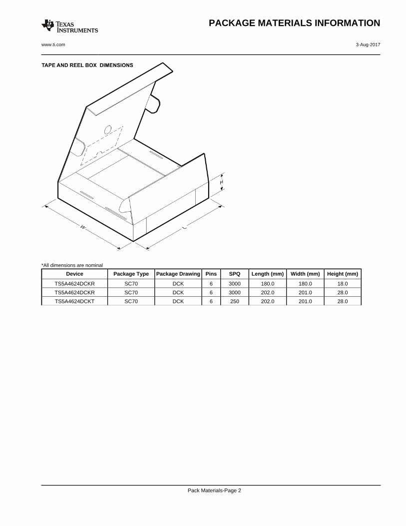
*All dimensions are nominal
Device Package Type Package Drawing Pins SPQ Length (mm) Width (mm) Height (mm)
TS5A4624DCKR SC70 DCK 6 3000 180.0 180.0 18.0
TS5A4624DCKR SC70 DCK 6 3000 202.0 201.0 28.0
TS5A4624DCKT SC70 DCK 6 250 202.0 201.0 28.0
PACKAGE MATERIALS INFORMATION
www.ti.com 3-Aug-2017
Pack Materials-Page 2


IMPORTANT NOTICE
Texas Instruments Incorporated (TI) reserves the right to make corrections, enhancements, improvements and other changes to itssemiconductor products and services per JESD46, latest issue, and to discontinue any product or service per JESD48, latest issue. Buyersshould obtain the latest relevant information before placing orders and should verify that such information is current and complete.TI’s published terms of sale for semiconductor products (http://www.ti.com/sc/docs/stdterms.htm) apply to the sale of packaged integratedcircuit products that TI has qualified and released to market. Additional terms may apply to the use or sale of other types of TI products andservices.Reproduction of significant portions of TI information in TI data sheets is permissible only if reproduction is without alteration and isaccompanied by all associated warranties, conditions, limitations, and notices. TI is not responsible or liable for such reproduceddocumentation. Information of third parties may be subject to additional restrictions. Resale of TI products or services with statementsdifferent from or beyond the parameters stated by TI for that product or service voids all express and any implied warranties for theassociated TI product or service and is an unfair and deceptive business practice. TI is not responsible or liable for any such statements.Buyers and others who are developing systems that incorporate TI products (collectively, “Designers”) understand and agree that Designersremain responsible for using their independent analysis, evaluation and judgment in designing their applications and that Designers havefull and exclusive responsibility to assure the safety of Designers' applications and compliance of their applications (and of all TI productsused in or for Designers’ applications) with all applicable regulations, laws and other applicable requirements. Designer represents that, withrespect to their applications, Designer has all the necessary expertise to create and implement safeguards that (1) anticipate dangerousconsequences of failures, (2) monitor failures and their consequences, and (3) lessen the likelihood of failures that might cause harm andtake appropriate actions. Designer agrees that prior to using or distributing any applications that include TI products, Designer willthoroughly test such applications and the functionality of such TI products as used in such applications.TI’s provision of technical, application or other design advice, quality characterization, reliability data or other services or information,including, but not limited to, reference designs and materials relating to evaluation modules, (collectively, “TI Resources”) are intended toassist designers who are developing applications that incorporate TI products; by downloading, accessing or using TI Resources in anyway, Designer (individually or, if Designer is acting on behalf of a company, Designer’s company) agrees to use any particular TI Resourcesolely for this purpose and subject to the terms of this Notice.TI’s provision of TI Resources does not expand or otherwise alter TI’s applicable published warranties or warranty disclaimers for TIproducts, and no additional obligations or liabilities arise from TI providing such TI Resources. TI reserves the right to make corrections,enhancements, improvements and other changes to its TI Resources. TI has not conducted any testing other than that specificallydescribed in the published documentation for a particular TI Resource.Designer is authorized to use, copy and modify any individual TI Resource only in connection with the development of applications thatinclude the TI product(s) identified in such TI Resource. NO OTHER LICENSE, EXPRESS OR IMPLIED, BY ESTOPPEL OR OTHERWISETO ANY OTHER TI INTELLECTUAL PROPERTY RIGHT, AND NO LICENSE TO ANY TECHNOLOGY OR INTELLECTUAL PROPERTYRIGHT OF TI OR ANY THIRD PARTY IS GRANTED HEREIN, including but not limited to any patent right, copyright, mask work right, orother intellectual property right relating to any combination, machine, or process in which TI products or services are used. Informationregarding or referencing third-party products or services does not constitute a license to use such products or services, or a warranty orendorsement thereof. Use of TI Resources may require a license from a third party under the patents or other intellectual property of thethird party, or a license from TI under the patents or other intellectual property of TI.TI RESOURCES ARE PROVIDED “AS IS” AND WITH ALL FAULTS. TI DISCLAIMS ALL OTHER WARRANTIES ORREPRESENTATIONS, EXPRESS OR IMPLIED, REGARDING RESOURCES OR USE THEREOF, INCLUDING BUT NOT LIMITED TOACCURACY OR COMPLETENESS, TITLE, ANY EPIDEMIC FAILURE WARRANTY AND ANY IMPLIED WARRANTIES OFMERCHANTABILITY, FITNESS FOR A PARTICULAR PURPOSE, AND NON-INFRINGEMENT OF ANY THIRD PARTY INTELLECTUALPROPERTY RIGHTS. TI SHALL NOT BE LIABLE FOR AND SHALL NOT DEFEND OR INDEMNIFY DESIGNER AGAINST ANY CLAIM,INCLUDING BUT NOT LIMITED TO ANY INFRINGEMENT CLAIM THAT RELATES TO OR IS BASED ON ANY COMBINATION OFPRODUCTS EVEN IF DESCRIBED IN TI RESOURCES OR OTHERWISE. IN NO EVENT SHALL TI BE LIABLE FOR ANY ACTUAL,DIRECT, SPECIAL, COLLATERAL, INDIRECT, PUNITIVE, INCIDENTAL, CONSEQUENTIAL OR EXEMPLARY DAMAGES INCONNECTION WITH OR ARISING OUT OF TI RESOURCES OR USE THEREOF, AND REGARDLESS OF WHETHER TI HAS BEENADVISED OF THE POSSIBILITY OF SUCH DAMAGES.Unless TI has explicitly designated an individual product as meeting the requirements of a particular industry standard (e.g., ISO/TS 16949and ISO 26262), TI is not responsible for any failure to meet such industry standard requirements.Where TI specifically promotes products as facilitating functional safety or as compliant with industry functional safety standards, suchproducts are intended to help enable customers to design and create their own applications that meet applicable functional safety standardsand requirements. Using products in an application does not by itself establish any safety features in the application. Designers mustensure compliance with safety-related requirements and standards applicable to their applications. Designer may not use any TI products inlife-critical medical equipment unless authorized officers of the parties have executed a special contract specifically governing such use.Life-critical medical equipment is medical equipment where failure of such equipment would cause serious bodily injury or death (e.g., lifesupport, pacemakers, defibrillators, heart pumps, neurostimulators, and implantables). Such equipment includes, without limitation, allmedical devices identified by the U.S. Food and Drug Administration as Class III devices and equivalent classifications outside the U.S.TI may expressly designate certain products as completing a particular qualification (e.g., Q100, Military Grade, or Enhanced Product).Designers agree that it has the necessary expertise to select the product with the appropriate qualification designation for their applicationsand that proper product selection is at Designers’ own risk. Designers are solely responsible for compliance with all legal and regulatoryrequirements in connection with such selection.Designer will fully indemnify TI and its representatives against any damages, costs, losses, and/or liabilities arising out of Designer’s non-compliance with the terms and provisions of this Notice.
Mailing Address: Texas Instruments, Post Office Box 655303, Dallas, Texas 75265Copyright © 2017, Texas Instruments Incorporated
Related Documents

![Web of Knowledge [v.5.5] - All Databases Results](https://static.cupdf.com/doc/110x72/61fc81298d33c02b785df2a9/web-of-knowledge-v55-all-databases-results.jpg)