ETSI TS 125 141 V12.6.0 (2015-01) Universal Mobile Telecommunications System (UMTS); Base Station (BS) conformance testing (FDD) (3GPP TS 25.141 version 12.6.0 Release 12) TECHNICAL SPECIFICATION

Welcome message from author
This document is posted to help you gain knowledge. Please leave a comment to let me know what you think about it! Share it to your friends and learn new things together.
Transcript

ETSI TS 125 141 V12.6.0 (2015-01)
Universal Mobile Telecommunications System (UMTS); Base Station (BS) conformance testing (FDD) (3GPP TS 25.141 version 12.6.0 Release 12)
TECHNICAL SPECIFICATION

ETSI
ETSI TS 125 141 V12.6.0 (2015-01)13GPP TS 25.141 version 12.6.0 Release 12
Reference RTS/TSGR-0425141vc60
Keywords UMTS
ETSI
650 Route des Lucioles F-06921 Sophia Antipolis Cedex - FRANCE
Tel.: +33 4 92 94 42 00 Fax: +33 4 93 65 47 16
Siret N° 348 623 562 00017 - NAF 742 C
Association à but non lucratif enregistrée à la Sous-Préfecture de Grasse (06) N° 7803/88
Important notice
The present document can be downloaded from: http://www.etsi.org
The present document may be made available in electronic versions and/or in print. The content of any electronic and/or print versions of the present document shall not be modified without the prior written authorization of ETSI. In case of any
existing or perceived difference in contents between such versions and/or in print, the only prevailing document is the print of the Portable Document Format (PDF) version kept on a specific network drive within ETSI Secretariat.
Users of the present document should be aware that the document may be subject to revision or change of status. Information on the current status of this and other ETSI documents is available at
http://portal.etsi.org/tb/status/status.asp
If you find errors in the present document, please send your comment to one of the following services: http://portal.etsi.org/chaircor/ETSI_support.asp
Copyright Notification
No part may be reproduced or utilized in any form or by any means, electronic or mechanical, including photocopying and microfilm except as authorized by written permission of ETSI.
The content of the PDF version shall not be modified without the written authorization of ETSI. The copyright and the foregoing restriction extend to reproduction in all media.
© European Telecommunications Standards Institute 2015.
All rights reserved.
DECTTM, PLUGTESTSTM, UMTSTM and the ETSI logo are Trade Marks of ETSI registered for the benefit of its Members. 3GPPTM and LTE™ are Trade Marks of ETSI registered for the benefit of its Members and
of the 3GPP Organizational Partners. GSM® and the GSM logo are Trade Marks registered and owned by the GSM Association.

ETSI
ETSI TS 125 141 V12.6.0 (2015-01)23GPP TS 25.141 version 12.6.0 Release 12
Intellectual Property Rights IPRs essential or potentially essential to the present document may have been declared to ETSI. The information pertaining to these essential IPRs, if any, is publicly available for ETSI members and non-members, and can be found in ETSI SR 000 314: "Intellectual Property Rights (IPRs); Essential, or potentially Essential, IPRs notified to ETSI in respect of ETSI standards", which is available from the ETSI Secretariat. Latest updates are available on the ETSI Web server (http://ipr.etsi.org).
Pursuant to the ETSI IPR Policy, no investigation, including IPR searches, has been carried out by ETSI. No guarantee can be given as to the existence of other IPRs not referenced in ETSI SR 000 314 (or the updates on the ETSI Web server) which are, or may be, or may become, essential to the present document.
Foreword This Technical Specification (TS) has been produced by ETSI 3rd Generation Partnership Project (3GPP).
The present document may refer to technical specifications or reports using their 3GPP identities, UMTS identities or GSM identities. These should be interpreted as being references to the corresponding ETSI deliverables.
The cross reference between GSM, UMTS, 3GPP and ETSI identities can be found under http://webapp.etsi.org/key/queryform.asp.
Modal verbs terminology In the present document "shall", "shall not", "should", "should not", "may", "may not", "need", "need not", "will", "will not", "can" and "cannot" are to be interpreted as described in clause 3.2 of the ETSI Drafting Rules (Verbal forms for the expression of provisions).
"must" and "must not" are NOT allowed in ETSI deliverables except when used in direct citation.

ETSI
ETSI TS 125 141 V12.6.0 (2015-01)33GPP TS 25.141 version 12.6.0 Release 12
Contents
Intellectual Property Rights ................................................................................................................................ 2
Foreword ............................................................................................................................................................. 2
Modal verbs terminology .................................................................................................................................... 2
Foreword ........................................................................................................................................................... 15
1 Scope ...................................................................................................................................................... 16
2 References .............................................................................................................................................. 16
3 Definitions and abbreviations ................................................................................................................. 17
3.1 Definitions ........................................................................................................................................................ 17
3.2 Symbols ............................................................................................................................................................ 19
3.3 Abbreviations ................................................................................................................................................... 20
3.4 Radio Frequency bands .................................................................................................................................... 21
3.4.1 Frequency bands ......................................................................................................................................... 21
3.4.2 TX-RX frequency separation ...................................................................................................................... 23
3.5 Channel arrangement ........................................................................................................................................ 24
3.5.1 Channel spacing .......................................................................................................................................... 24
3.5.2 Channel raster ............................................................................................................................................. 24
3.5.3 Channel number .......................................................................................................................................... 25
4 General test conditions and declarations ................................................................................................ 26
4.1 Acceptable uncertainty of Test System ............................................................................................................ 27
4.1.1 Measurement of test environments ............................................................................................................. 27
4.1.2 Measurement of transmitter ........................................................................................................................ 28
4.1.3 Measurement of receiver ............................................................................................................................ 30
4.1.4 Measurement of performance requirement ................................................................................................. 31
4.2 Test Tolerances (informative) .......................................................................................................................... 32
4.2.1 Transmitter .................................................................................................................................................. 33
4.2.2 Receiver ...................................................................................................................................................... 33
4.2.3 Performance requirement ............................................................................................................................ 34
4.2.4 RRM measurements .................................................................................................................................... 34
4.3 Interpretation of measurement results .............................................................................................................. 34
4.3A Base station classes .......................................................................................................................................... 35
4.4 Test environments ............................................................................................................................................ 35
4.4.1 Normal test environment ............................................................................................................................ 35
4.4.2 Extreme test environment ........................................................................................................................... 35
4.4.2.1 Extreme temperature ............................................................................................................................. 36
4.4.3 Vibration ..................................................................................................................................................... 36
4.4.4 Power supply .............................................................................................................................................. 36
4.4.5 Definition of Additive White Gaussian Noise (AWGN) Interferer ............................................................ 36
4.5 Selection of configurations for testing.............................................................................................................. 36
4.6 BS Configurations ............................................................................................................................................ 37
4.6.1 Receiver diversity ....................................................................................................................................... 37
4.6.2 Duplexers .................................................................................................................................................... 37
4.6.3 Power supply options .................................................................................................................................. 37
4.6.4 Ancillary RF amplifiers .............................................................................................................................. 38
4.6.5 BS using antenna arrays .............................................................................................................................. 38
4.6.5.1 Receiver tests ........................................................................................................................................ 39
4.6.5.2 Transmitter tests .................................................................................................................................... 39
4.6.6 Transmit diversity and MIMO transmission ............................................................................................... 39
4.6.7 BS with integrated Iuant BS modem .......................................................................................................... 40
4.6.8 BS with Virtual Antenna Mapping ............................................................................................................. 40
4.7 Regional requirements ...................................................................................................................................... 41
4.8 Specified frequency range ................................................................................................................................ 43
4.8.1 RF bandwidth position for non-single carrier testing ................................................................................. 43
4.9 Applicability of requirements ........................................................................................................................... 44

ETSI
ETSI TS 125 141 V12.6.0 (2015-01)43GPP TS 25.141 version 12.6.0 Release 12
4.10 Requirements for contiguous and non-contiguous spectrum ............................................................................ 44
4.11 Manufacturer"s declarations of regional and optional requirements ................................................................ 44
4.11.1 Operating band and frequency range .......................................................................................................... 44
4.11.2 Spurious emissions category ....................................................................................................................... 44
4.11.3 Additional out of band emissions ............................................................................................................... 45
4.11.4 Co-existence with other systems ................................................................................................................. 45
4.11.5 Co-location with other base stations ........................................................................................................... 45
4.11.6 Manufacturer's declarations of supported RF configurations ..................................................................... 45
4.12 Test configuration for multi-carrier operations ................................................................................................ 46
4.12.1 UTC1: Contiguous spectrum operation test configuration ......................................................................... 47
4.12.1.1 UTC1 power allocation ......................................................................................................................... 47
4.12.2 UTC2:Non-contiguous spectrum operation test configuration ................................................................... 47
4.12.2.1 UTC2 power allocation ......................................................................................................................... 47
4.12.3 Multi-band operation test configurations .................................................................................................... 47
4.12.3.1 UTC3: Multi-band test configuration for full carrier allocation ............................................................ 47
4.12.3.1.1 UTC3 power allocation ................................................................................................................... 48
4.12.3.2 UTC4: Multi-band test configuration with high PSD per carrier .......................................................... 48
4.12.3.2.1 UTC4 power allocation ................................................................................................................... 49
4.12.4 Applicability of test configurations ............................................................................................................ 49
4.13 Requirements for BS capable of multi-band operation .................................................................................... 51
5 Format and interpretation of tests ........................................................................................................... 52
6 Transmitter ............................................................................................................................................. 52
6.1 General ............................................................................................................................................................. 52
6.1.1 Test Models ................................................................................................................................................ 53
6.1.1.1 Test Model 1 – TM1 ............................................................................................................................. 53
6.1.1.2 Test Model 2 – TM2 ............................................................................................................................. 56
6.1.1.3 Test Model 3 – TM3 ............................................................................................................................. 56
6.1.1.4 Test Model 4 – TM4 ............................................................................................................................. 57
6.1.1.4A Test Model 5 – TM5 ............................................................................................................................. 58
6.1.1.4B Test Model 6 – TM6 ............................................................................................................................. 59
6.1.1.5 DPCH Structure of the Downlink Test Models ..................................................................................... 61
6.1.1.6 Common channel Structure of the Downlink Test Models ................................................................... 62
6.1.1.6.1 P-CCPCH ........................................................................................................................................ 62
6.1.1.6.2 PICH ................................................................................................................................................ 62
6.1.1.6.3 Primary scrambling code and SCH.................................................................................................. 62
6.1.1.6.4 S-CCPCH containing PCH .............................................................................................................. 62
6.1.1.7 HS-PDSCH Structure of the Downlink TM5 ........................................................................................ 63
6.1.1.8 HS-SCCH Structure of the Downlink Test Models 5 and 6 .................................................................. 63
6.1.1.9 HS-PDSCH Structure of the Downlink TM6 ........................................................................................ 63
6.2 Base station output power ................................................................................................................................ 63
6.2.1 Base station maximum output power .......................................................................................................... 63
6.2.1.1 Definition and applicability ................................................................................................................... 63
6.2.1.2 Minimum Requirement ......................................................................................................................... 64
6.2.1.3 Test purpose .......................................................................................................................................... 64
6.2.1.4 Method of test ....................................................................................................................................... 64
6.2.1.4.1 Initial conditions .............................................................................................................................. 64
6.2.1.4.2 Procedure ......................................................................................................................................... 64
6.2.1.5 Test Requirements ................................................................................................................................. 65
6.2.2 Primary CPICH power accuracy ................................................................................................................. 65
6.2.2.1 Definition and applicability ................................................................................................................... 65
6.2.2.2 Minimum Requirement ......................................................................................................................... 65
6.2.2.3 Test purpose .......................................................................................................................................... 65
6.2.2.4 Method of test ....................................................................................................................................... 65
6.2.2.4.1 Initial conditions .............................................................................................................................. 65
6.2.2.4.2 Procedure ......................................................................................................................................... 65
6.2.2.5 Test Requirement .................................................................................................................................. 66
6.2.3 Secondary CPICH power offset accuracy ................................................................................................... 66
6.2.3.1 Definition and applicability ................................................................................................................... 66
6.2.3.2 Minimum Requirement ......................................................................................................................... 66
6.2.3.3 Test purpose .......................................................................................................................................... 66

ETSI
ETSI TS 125 141 V12.6.0 (2015-01)53GPP TS 25.141 version 12.6.0 Release 12
6.2.3.4 Method of test for MIMO mode ............................................................................................................ 66
6.2.3.4.1 Initial conditions .............................................................................................................................. 66
6.2.3.4.2 Procedure ......................................................................................................................................... 67
6.2.3.4A Method of test for MIMO mode with four transmit antennas ............................................................... 67
6.2.3.4A.1 Initial conditions .............................................................................................................................. 67
6.2.3.4A.2 Procedure ......................................................................................................................................... 67
6.2.3.5 Test Requirement for MIMO mode ...................................................................................................... 67
6.2.3.5A Test Requirement for MIMO mode with four transmit antennas .......................................................... 67
6.3 Frequency error ................................................................................................................................................ 68
6.3.1 Definition and applicability ........................................................................................................................ 68
6.3.2 Minimum Requirement ............................................................................................................................... 68
6.3.3 Test purpose ................................................................................................................................................ 68
6.3.4 Method of test ............................................................................................................................................. 68
6.3.5 Test requirement ......................................................................................................................................... 68
6.4 Output power dynamics .................................................................................................................................... 68
6.4.1 Inner loop power control ............................................................................................................................. 68
6.4.2 Power control steps ..................................................................................................................................... 69
6.4.2.1 Definition and applicability ................................................................................................................... 69
6.4.2.2 Minimum Requirement ......................................................................................................................... 69
6.4.2.3 Test purpose .......................................................................................................................................... 69
6.4.2.4 Method of test ....................................................................................................................................... 69
6.4.2.4.1 Initial conditions .............................................................................................................................. 69
6.4.2.4.2 Procedure ......................................................................................................................................... 69
6.4.2.5 Test requirement ................................................................................................................................... 70
6.4.3 Power control dynamic range ..................................................................................................................... 70
6.4.3.1 Definition and applicability ................................................................................................................... 70
6.4.3.2 Minimum Requirement ......................................................................................................................... 70
6.4.3.3 Test purpose .......................................................................................................................................... 70
6.4.3.4 Method of test ....................................................................................................................................... 71
6.4.3.4.1 Initial conditions .............................................................................................................................. 71
6.4.3.4.2 Procedure ......................................................................................................................................... 71
6.4.3.5 Test requirement ................................................................................................................................... 71
6.4.4 Total power dynamic range ........................................................................................................................ 71
6.4.4.1 Definition and applicability ................................................................................................................... 71
6.4.4.2 Minimum Requirement ......................................................................................................................... 71
6.4.4.3 Test purpose .......................................................................................................................................... 71
6.4.4.4 Method of test ....................................................................................................................................... 72
6.4.4.4.1 Initial Conditions ............................................................................................................................. 72
6.4.4.4.2 Procedure ......................................................................................................................................... 72
6.4.4.5 Test requirement ................................................................................................................................... 72
6.4.5 IPDL time mask .......................................................................................................................................... 72
6.4.5.1 Definition and applicability ................................................................................................................... 72
6.4.5.2 Minimum Requirement ......................................................................................................................... 72
6.4.5.3 Test purpose .......................................................................................................................................... 72
6.4.5.4 Method of test ....................................................................................................................................... 73
6.4.5.4.1 Initial conditions .............................................................................................................................. 73
6.4.5.4.2 Procedure ......................................................................................................................................... 73
6.4.5.5 Test Requirements ................................................................................................................................. 73
6.4.6 Home base station output power for adjacent channel protection ............................................................... 74
6.4.6.1 Definition and applicability ................................................................................................................... 74
6.4.6.2 Minimum Requirement ......................................................................................................................... 74
6.4.6.3 Test purpose .......................................................................................................................................... 74
6.4.6.4 Method of test ....................................................................................................................................... 75
6.4.6.4.1 Initial conditions .............................................................................................................................. 75
6.4.6.4.2 Procedure ......................................................................................................................................... 75
6.4.6.5 Test Requirements ................................................................................................................................. 75
6.5 Output RF spectrum emissions ......................................................................................................................... 76
6.5.1 Occupied bandwidth ................................................................................................................................... 76
6.5.1.1 Definition and applicability ................................................................................................................... 76
6.5.1.2 Minimum Requirements ........................................................................................................................ 76
6.5.1.3 Test purpose .......................................................................................................................................... 76
6.5.1.4 Method of test ....................................................................................................................................... 76

ETSI
ETSI TS 125 141 V12.6.0 (2015-01)63GPP TS 25.141 version 12.6.0 Release 12
6.5.1.4.1 Initial conditions .............................................................................................................................. 76
6.5.1.4.2 Procedure ......................................................................................................................................... 76
6.5.1.5 Test requirements .................................................................................................................................. 77
6.5.2 Out of band emission .................................................................................................................................. 77
6.5.2.1 Spectrum emission mask ....................................................................................................................... 77
6.5.2.1.1 Definitions and applicability ........................................................................................................... 77
6.5.2.1.2 Minimum Requirements .................................................................................................................. 77
6.5.2.1.3 Test purpose .................................................................................................................................... 78
6.5.2.1.4 Method of test .................................................................................................................................. 78
6.5.2.1.4.1 Initial conditions ........................................................................................................................ 78
6.5.2.1.4.2 Procedures ....................................................................................................................................... 78
6.5.2.1.5 Test requirements ............................................................................................................................ 78
6.5.2.2 Adjacent Channel Leakage power Ratio (ACLR) ................................................................................. 86
6.5.2.2.1 Definition and applicability ............................................................................................................. 86
6.5.2.2.2 Minimum Requirement ................................................................................................................... 86
6.5.2.2.3 Test purpose .................................................................................................................................... 86
6.5.2.2.4 Method of test .................................................................................................................................. 86
6.5.2.2.4.1 Initial conditions ........................................................................................................................ 86
6.5.2.2.4.2 Procedure ................................................................................................................................... 87
6.5.2.2.5 Test Requirement............................................................................................................................. 87
6.5.2.2.6 Cumulative ACLR test requirement in non-contiguous spectrum or multiple-bands ...................... 88
6.5.3 Spurious emissions ..................................................................................................................................... 89
6.5.3.1 Definition and applicability ................................................................................................................... 89
6.5.3.2 (void) ..................................................................................................................................................... 89
6.5.3.3 (void) ..................................................................................................................................................... 89
6.5.3.4 Minimum Requirements ........................................................................................................................ 89
6.5.3.5 Test purpose .......................................................................................................................................... 90
6.5.3.6 Method of Test ...................................................................................................................................... 90
6.5.3.6.1 Initial conditions .............................................................................................................................. 90
6.5.3.6.2 Procedure ......................................................................................................................................... 91
6.5.3.7 Test requirements .................................................................................................................................. 91
6.5.3.7.1 Spurious emissions (Category A) .................................................................................................... 91
6.5.3.7.2 Spurious emissions (Category B) .................................................................................................... 91
6.5.3.7.3 Protection of the BS receiver of own or different BS ...................................................................... 92
6.5.3.7.4 Co-existence with other systems in the same geographical area ..................................................... 94
6.5.3.7.5 Co-existence with co-located and co-sited base stations ................................................................. 98
6.5.3.7.6 Co-existence with PHS .................................................................................................................. 104
6.5.3.7.7 Co-existence with services in adjacent frequency bands ............................................................... 104
6.5.3.7.8 Void ............................................................................................................................................... 104
6.5.3.7.8.1 Void ......................................................................................................................................... 104
6.5.3.7.8.2 Void ......................................................................................................................................... 104
6.5.3.7.9 Protection of Public Safety Operations .......................................................................................... 104
6.5.3.7.10 Co-existence with Home BS operating in other bands .................................................................. 105
6.6 Transmitter intermodulation ........................................................................................................................... 107
6.6.1 Definition and applicability ...................................................................................................................... 107
6.6.2 Minimum Requirement ............................................................................................................................. 107
6.6.3 Test purpose .............................................................................................................................................. 107
6.6.4 Method of test ........................................................................................................................................... 107
6.6.4.1 Initial conditions ................................................................................................................................. 107
6.6.4.2 Procedures ........................................................................................................................................... 108
6.6.5 Test Requirements .................................................................................................................................... 108
6.7 Transmit modulation ...................................................................................................................................... 109
6.7.1 Error Vector Magnitude ............................................................................................................................ 109
6.7.1.1 Definition and applicability ................................................................................................................. 109
6.7.1.2 Minimum Requirement ....................................................................................................................... 109
6.7.1.3 Test Purpose ........................................................................................................................................ 109
6.7.1.4 Method of Test .................................................................................................................................... 109
6.7.1.4.1 Initial Conditions ........................................................................................................................... 109
6.7.1.4.2 Procedure ....................................................................................................................................... 109
6.7.1.5 Test Requirement ................................................................................................................................ 110
6.7.2 Peak Code Domain Error .......................................................................................................................... 110
6.7.2.1 Definition and applicability ................................................................................................................. 110

ETSI
ETSI TS 125 141 V12.6.0 (2015-01)73GPP TS 25.141 version 12.6.0 Release 12
6.7.2.2 Minimum requirement ........................................................................................................................ 110
6.7.2.3 Test Purpose ........................................................................................................................................ 110
6.7.2.4 Method of test ..................................................................................................................................... 110
6.7.2.4.1 Initial conditions ............................................................................................................................ 110
6.7.2.4.2 Procedure ....................................................................................................................................... 110
6.7.2.5 Test requirement ................................................................................................................................. 111
6.7.3 Time alignment error ................................................................................................................................ 111
6.7.3.1 Definition and applicability ................................................................................................................. 111
6.7.3.2 Minimum Requirement ....................................................................................................................... 111
6.7.3.3 Test Purpose ........................................................................................................................................ 111
6.7.3.4 Method of Test .................................................................................................................................... 111
6.7.3.4.1 Initial Conditions ........................................................................................................................... 111
6.7.3.4.2 Procedure ....................................................................................................................................... 112
6.7.3.5 Test Requirement ................................................................................................................................ 112
6.7.4 Relative Code Domain Error .................................................................................................................... 112
6.7.4.1 Definition and applicability ................................................................................................................. 112
6.7.4.2 Minimum requirement ........................................................................................................................ 112
6.7.4.3 Test Purpose ........................................................................................................................................ 112
6.7.4.4 Method of test ..................................................................................................................................... 113
6.7.4.4.1 Initial conditions ............................................................................................................................ 113
6.7.4.4.2 Procedure ....................................................................................................................................... 113
6.7.4.5 Test requirement ................................................................................................................................. 113
7 Receiver characteristics ........................................................................................................................ 113
7.1 General ........................................................................................................................................................... 113
7.2 Reference sensitivity level .............................................................................................................................. 114
7.2.1 Definition and applicability ...................................................................................................................... 114
7.2.2 Minimum Requirement ............................................................................................................................. 114
7.2.3 Test purpose .............................................................................................................................................. 114
7.2.4 Method of testing ...................................................................................................................................... 115
7.2.4.1 Initial conditions ................................................................................................................................. 115
7.2.4.2 Procedure ............................................................................................................................................ 115
7.2.5 Test requirement ....................................................................................................................................... 115
7.3 Dynamic range ............................................................................................................................................... 116
7.3.1 Definition and applicability ...................................................................................................................... 116
7.3.2 Minimum Requirement ............................................................................................................................. 116
7.3.3 Test purpose .............................................................................................................................................. 116
7.3.4 Method of test ........................................................................................................................................... 116
7.3.4.1 Initial conditions ................................................................................................................................. 116
7.3.4.2 Procedure ............................................................................................................................................ 116
7.3.5 Test Requirements .................................................................................................................................... 116
7.4 Adjacent Channel Selectivity (ACS) .............................................................................................................. 117
7.4.1 Definition and applicability ...................................................................................................................... 117
7.4.2 Minimum Requirement ............................................................................................................................. 117
7.4.3 Test purpose .............................................................................................................................................. 117
7.4.4 Method of test ........................................................................................................................................... 117
7.4.4.1 Initial conditions ................................................................................................................................. 117
7.4.4.2 Procedure ............................................................................................................................................ 117
7.4.5 Test Requirements .................................................................................................................................... 118
7.5 Blocking characteristics ................................................................................................................................. 118
7.5.1 Definition and applicability ...................................................................................................................... 118
7.5.2 Minimum Requirements ........................................................................................................................... 119
7.5.3 Test purpose .............................................................................................................................................. 119
7.5.4 Method of test ........................................................................................................................................... 119
7.5.4.1 Initial conditions ................................................................................................................................. 119
7.5.4.2 Procedure ............................................................................................................................................ 120
7.5.5 Test Requirements .................................................................................................................................... 120
7.6 Intermodulation characteristics ...................................................................................................................... 134
7.6.1 Definition and applicability ...................................................................................................................... 134
7.6.2 Minimum Requirement ............................................................................................................................. 134
7.6.3 Test purpose .............................................................................................................................................. 134
7.6.4 Method of test ........................................................................................................................................... 135

ETSI
ETSI TS 125 141 V12.6.0 (2015-01)83GPP TS 25.141 version 12.6.0 Release 12
7.6.4.1 Initial conditions ................................................................................................................................. 135
7.6.4.2 Procedures ........................................................................................................................................... 135
7.6.5 Test requirements ...................................................................................................................................... 135
7.7 Spurious Emissions ........................................................................................................................................ 136
7.7.1 Definition and applicability ...................................................................................................................... 136
7.7.2 Minimum Requirements ........................................................................................................................... 136
7.7.3 Test purpose .............................................................................................................................................. 136
7.7.4 Method of test ........................................................................................................................................... 136
7.7.4.1 Initial conditions ................................................................................................................................. 136
7.7.4.2 Procedure ............................................................................................................................................ 137
7.7.5 Test requirements ...................................................................................................................................... 137
7.8 Verification of the internal BER calculation .................................................................................................. 138
7.8.1 Definition and applicability ...................................................................................................................... 138
7.8.2 Minimum Requirement ............................................................................................................................. 138
7.8.3 Test purpose .............................................................................................................................................. 138
7.8.4 Method of test ........................................................................................................................................... 138
7.8.4.1 Initial conditions ................................................................................................................................. 138
7.8.4.2 Procedure ............................................................................................................................................ 139
7.8.5 Test Requirement ...................................................................................................................................... 139
8 Performance requirement ..................................................................................................................... 139
8.1 General ........................................................................................................................................................... 139
8.2 Demodulation in static propagation conditions .............................................................................................. 140
8.2.1 Demodulation of DCH .............................................................................................................................. 140
8.2.1.1 Definition and applicability ................................................................................................................. 140
8.2.1.2 Minimum requirement ........................................................................................................................ 140
8.2.1.3 Test purpose ........................................................................................................................................ 140
8.2.1.4 Method of test ..................................................................................................................................... 140
8.2.1.4.1 Initial conditions ............................................................................................................................ 140
8.2.1.4.2 Procedure ....................................................................................................................................... 140
8.2.1.5 Test requirements ................................................................................................................................ 140
8.3 Demodulation of DCH in multipath fading conditions .................................................................................. 141
8.3.1 Multipath fading Case 1 ............................................................................................................................ 141
8.3.1.1 Definition and applicability ................................................................................................................. 141
8.3.1.2 Minimum requirement ........................................................................................................................ 141
8.3.1.3 Test Purpose ........................................................................................................................................ 141
8.3.1.4 Method of test ..................................................................................................................................... 141
8.3.1.4.1 Initial conditions ............................................................................................................................ 141
8.3.1.4.2 Procedure ....................................................................................................................................... 141
8.3.1.5 Test requirements ................................................................................................................................ 142
8.3.2 Multipath fading Case 2 ............................................................................................................................ 142
8.3.2.1 Definition and applicability ................................................................................................................. 142
8.3.2.2 Minimum requirement ........................................................................................................................ 142
8.3.2.3 Test Purpose ........................................................................................................................................ 142
8.3.2.4 Method of test ..................................................................................................................................... 143
8.3.2.4.1 Initial conditions ............................................................................................................................ 143
8.3.2.4.2 Procedure ....................................................................................................................................... 143
8.3.2.5 Test requirements ................................................................................................................................ 143
8.3.3 Multipath fading Case 3 ............................................................................................................................ 144
8.3.3.1 Definition and applicability ................................................................................................................. 144
8.3.3.2 Minimum requirement ........................................................................................................................ 144
8.3.3.3 Test purpose ........................................................................................................................................ 144
8.3.3.4 Method of test ..................................................................................................................................... 144
8.3.3.4.1 Initial conditions ............................................................................................................................ 144
8.3.3.4.2 Procedure ....................................................................................................................................... 144
8.3.3.5 Test requirements ................................................................................................................................ 144
8.3.4 Multipath fading Case 4 ............................................................................................................................ 145
8.3.4.1 Definition and applicability ................................................................................................................. 145
8.3.4.2 Minimum requirement ........................................................................................................................ 145
8.3.4.3 Test purpose ........................................................................................................................................ 145
8.3.4.4 Method of test ..................................................................................................................................... 145
8.3.4.4.1 Initial conditions ............................................................................................................................ 145

ETSI
ETSI TS 125 141 V12.6.0 (2015-01)93GPP TS 25.141 version 12.6.0 Release 12
8.3.4.4.2 Procedure ....................................................................................................................................... 145
8.3.4.5 Test requirements ................................................................................................................................ 146
8.4 Demodulation of DCH in moving propagation conditions ............................................................................. 146
8.4.1 Definition and applicability ...................................................................................................................... 146
8.4.2 Minimum requirement .............................................................................................................................. 146
8.4.3 Test purpose .............................................................................................................................................. 146
8.4.4 Method of test ........................................................................................................................................... 147
8.4.4.1 Initial conditions ................................................................................................................................. 147
8.4.4.2 Procedure ............................................................................................................................................ 147
8.4.5 Test requirements ...................................................................................................................................... 147
8.5 Demodulation of DCH in birth/death propagation conditions ........................................................................ 148
8.5.1 Definition and applicability ...................................................................................................................... 148
8.5.2 Minimum requirement .............................................................................................................................. 148
8.5.3 Test purpose .............................................................................................................................................. 148
8.5.4 Method of test ........................................................................................................................................... 148
8.5.4.1 Initial conditions ................................................................................................................................. 148
8.5.4.2 Procedure ............................................................................................................................................ 148
8.5.5 Test requirements ...................................................................................................................................... 149
8.5A Demodulation of DCH in high speed train conditions ................................................................................... 149
8.5A.1 Definition and applicability ...................................................................................................................... 149
8.5A.2 Minimum requirement .............................................................................................................................. 149
8.5A.3 Test purpose .............................................................................................................................................. 149
8.5A.4 Method of test ........................................................................................................................................... 149
8.5A.4.1 Initial conditions ................................................................................................................................. 149
8.5A.4.2 Procedure ............................................................................................................................................ 149
8.5A.5 Test requirements ...................................................................................................................................... 150
8.6 Verification of the internal BLER calculation ................................................................................................ 150
8.6.1 Definition and applicability ...................................................................................................................... 150
8.6.2 Minimum requirement .............................................................................................................................. 151
8.6.3 Test purpose .............................................................................................................................................. 151
8.6.4 Method of test ........................................................................................................................................... 151
8.6.4.1 Initial conditions ................................................................................................................................. 151
8.6.4.2 Procedure ............................................................................................................................................ 151
8.6.5 Test requirement ....................................................................................................................................... 151
8.7 (void) .............................................................................................................................................................. 152
8.8 RACH performance ........................................................................................................................................ 152
8.8.1 RACH preamble detection in static propagation conditions ..................................................................... 152
8.8.1.1 Definition and applicability ................................................................................................................. 152
8.8.1.2 Minimum requirement ........................................................................................................................ 152
8.8.1.3 Test purpose ........................................................................................................................................ 152
8.8.1.4 Method of test ..................................................................................................................................... 152
8.8.1.4.1 Initial conditions ............................................................................................................................ 152
8.8.1.4.2 Procedure ....................................................................................................................................... 152
8.8.1.5 Test requirements ................................................................................................................................ 153
8.8.2A RACH preamble detection in high speed train conditions ........................................................................ 153
8.8.2A.1 Definition and applicability ................................................................................................................. 153
8.8.2A.2 Minimum requirement ........................................................................................................................ 153
8.8.2A.3 Test purpose ........................................................................................................................................ 153
8.8.2A.4 Method of test ..................................................................................................................................... 153
8.8.2A.4.1 Initial conditions ............................................................................................................................ 153
8.8.2A.4.2 Procedure ....................................................................................................................................... 153
8.8.2A.5 Test requirements ................................................................................................................................ 154
8.8.2 RACH preamble detection in multipath fading case 3 .............................................................................. 154
8.8.2.1 Definition and applicability ................................................................................................................. 154
8.8.2.2 Minimum requirement ........................................................................................................................ 154
8.8.2.3 Test purpose ........................................................................................................................................ 155
8.8.2.4 Method of test ..................................................................................................................................... 155
8.8.2.4.1 Initial conditions ............................................................................................................................ 155
8.8.2.4.2 Procedure ....................................................................................................................................... 155
8.8.2.5 Test requirements ................................................................................................................................ 155
8.8.3 Demodulation of RACH message in static propagation conditions .......................................................... 156
8.8.3.1 Definition and applicability ................................................................................................................. 156
ETSI
ETSI TS 125 141 V12.6.0 (2015-01)103GPP TS 25.141 version 12.6.0 Release 12
8.8.3.2 Minimum requirement ........................................................................................................................ 156
8.8.3.3 Test purpose ........................................................................................................................................ 156
8.8.3.4 Method of test ..................................................................................................................................... 156
8.8.3.4.1 Initial conditions ............................................................................................................................ 156
8.8.3.4.2 Procedure ....................................................................................................................................... 156
8.8.3.5 Test requirements ................................................................................................................................ 157
8.8.4 Demodulation of RACH message in multipath fading case 3 .................................................................. 157
8.8.4.1 Definition and applicability ................................................................................................................. 157
8.8.4.2 Minimum requirement ........................................................................................................................ 157
8.8.4.3 Test purpose ........................................................................................................................................ 157
8.8.4.4 Method of test ..................................................................................................................................... 157
8.8.4.4.1 Initial conditions ............................................................................................................................ 157
8.8.4.4.2 Procedure ....................................................................................................................................... 158
8.8.4.5 Test requirements ................................................................................................................................ 158
8.8.5 Demodulation of RACH message in high speed train conditions ............................................................. 159
8.8.5.1 Definition and applicability ................................................................................................................. 159
8.8.5.2 Minimum requirement ........................................................................................................................ 159
8.8.5.3 Test purpose ........................................................................................................................................ 159
8.8.5.4 Method of test ..................................................................................................................................... 159
8.8.5.4.1 Initial conditions ............................................................................................................................ 159
8.8.5.4.2 Procedure ....................................................................................................................................... 159
8.8.5.5 Test requirements ................................................................................................................................ 160
8.9 (void) .............................................................................................................................................................. 160
8.10 (void) .............................................................................................................................................................. 161
8.11 Performance of signalling detection for HS-DPCCH ..................................................................................... 161
8.11.1 ACK false alarm in static propagation conditions .................................................................................... 161
8.11.1.1 Definition and applicability ................................................................................................................. 161
8.11.1.2 Minimum requirement ........................................................................................................................ 161
8.11.1.3 Test purpose ........................................................................................................................................ 161
8.11.1.4 Method of test ..................................................................................................................................... 161
8.11.1.4.1 Initial conditions ............................................................................................................................ 161
8.11.1.4.2 Procedure ....................................................................................................................................... 161
8.11.1.5 Test requirements ................................................................................................................................ 162
8.11.2 ACK false alarm in multipath fading conditions ...................................................................................... 162
8.11.2.1 Definition and applicability ................................................................................................................. 162
8.11.2.2 Minimum requirement ........................................................................................................................ 162
8.11.2.3 Test purpose ........................................................................................................................................ 162
8.11.2.4 Method of test ..................................................................................................................................... 162
8.11.2.4.1 Initial conditions ............................................................................................................................ 162
8.11.2.4.2 Procedure ....................................................................................................................................... 162
8.11.2.5 Test requirements ................................................................................................................................ 163
8.11.3 ACK mis-detection in static propagation conditions ................................................................................ 163
8.11.3.1 Definition and applicability ................................................................................................................. 163
8.11.3.2 Minimum requirement ........................................................................................................................ 163
8.11.3.3 Test purpose ........................................................................................................................................ 163
8.11.3.4 Method of test ..................................................................................................................................... 163
8.11.3.4.1 Initial conditions ............................................................................................................................ 163
8.11.3.4.2 Procedure ....................................................................................................................................... 164
8.11.3.5 Test requirements ................................................................................................................................ 164
8.11.4 ACK mis-detection in multipath fading conditions .................................................................................. 164
8.11.4.1 Definition and applicability ................................................................................................................. 164
8.11.4.2 Minimum requirement ........................................................................................................................ 164
8.11.4.3 Test purpose ........................................................................................................................................ 164
8.11.4.4 Method of test ..................................................................................................................................... 165
8.11.4.4.1 Initial conditions ............................................................................................................................ 165
8.11.4.4.2 Procedure ....................................................................................................................................... 165
8.11.4.5 Test requirements ................................................................................................................................ 165
8.11A Performance of signalling detection for 4C-HSDPA HS-DPCCH ................................................................. 165
8.11A.1 ACK false alarm for 4C-HSDPA in static propagation conditions ........................................................... 166
8.11A.1.1 Definition and applicability ................................................................................................................. 166
8.11A.1.2 Minimum requirement ........................................................................................................................ 166
8.11A.1.3 Test purpose ........................................................................................................................................ 166

ETSI
ETSI TS 125 141 V12.6.0 (2015-01)113GPP TS 25.141 version 12.6.0 Release 12
8.11A.1.4 Method of test ..................................................................................................................................... 166
8.11A.1.4.1 Initial conditions ............................................................................................................................ 166
8.11A.1.4.2 Procedure ....................................................................................................................................... 166
8.11A.1.5 Test requirements ................................................................................................................................ 167
8.11A.2 ACK false alarm for 4C-HSDPA in multipath fading conditions ............................................................. 167
8.11A.2.1 Definition and applicability ................................................................................................................. 167
8.11A.2.2 Minimum requirement ........................................................................................................................ 167
8.11A.2.3 Test purpose ........................................................................................................................................ 167
8.11A.2.4 Method of test ..................................................................................................................................... 167
8.11A.2.4.1 Initial conditions ............................................................................................................................ 167
8.11A.2.4.2 Procedure ....................................................................................................................................... 167
8.11A.2.5 Test requirements ................................................................................................................................ 168
8.11A.3 ACK mis-detection for 4C-HSDPA in static propagation conditions ....................................................... 168
8.11A.3.1 Definition and applicability ................................................................................................................. 168
8.11A.3.2 Minimum requirement ........................................................................................................................ 168
8.11A.3.3 Test purpose ........................................................................................................................................ 168
8.11A.3.4 Method of test ..................................................................................................................................... 169
8.11A.3.4.1 Initial conditions ............................................................................................................................ 169
8.11A.3.4.2 Procedure ....................................................................................................................................... 169
8.11A.3.5 Test requirements ................................................................................................................................ 169
8.11A.4 ACK mis-detection for 4C-HSDPA in multipath fading conditions ......................................................... 169
8.11A.4.1 Definition and applicability ................................................................................................................. 169
8.11A.4.2 Minimum requirement ........................................................................................................................ 170
8.11A.4.3 Test purpose ........................................................................................................................................ 170
8.11A.4.4 Method of test ..................................................................................................................................... 170
8.11A.4.4.1 Initial conditions ............................................................................................................................ 170
8.11A.4.4.2 Procedure ....................................................................................................................................... 170
8.11A.4.5 Test requirements ................................................................................................................................ 170
8.11B Performance of signalling detection for 8C-HSDPA HS-DPCCH ................................................................. 171
8.12 Demodulation of E-DPDCH in multipath fading conditions .......................................................................... 171
8.12.1 Definition and applicability ...................................................................................................................... 171
8.12.2 Minimum requirement .............................................................................................................................. 172
8.12.3 Test Purpose.............................................................................................................................................. 172
8.12.4 Method of test ........................................................................................................................................... 172
8.12.4.1 Initial conditions ................................................................................................................................. 172
8.12.4.2 Procedure ............................................................................................................................................ 172
8.12.4.3 Test requirements ................................................................................................................................ 172
8.12A Demodulation of E-DPDCH and S-E-DPDCH in multipath fading conditions for UL MIMO ..................... 173
8.12A.1 Definition and applicability ...................................................................................................................... 173
8.12A.2 Minimum requirement .............................................................................................................................. 173
8.12A.3 Test Purpose.............................................................................................................................................. 174
8.12A.4 Method of test ........................................................................................................................................... 174
8.12A.4.1 Initial conditions ................................................................................................................................. 174
8.12A.4.2 Procedure ............................................................................................................................................ 174
8.12A.4.3 Test requirements ................................................................................................................................ 174
8.13 Performance of signalling detection for E-DPCCH in multipath fading conditions ...................................... 175
8.13.1 E-DPCCH false alarm in multipath fading conditions .............................................................................. 175
8.13.1.1 Definition and applicability ................................................................................................................. 175
8.13.1.2 Minimum requirement ........................................................................................................................ 175
8.13.1.3 Test purpose ........................................................................................................................................ 175
8.13.1.4 Method of test ..................................................................................................................................... 175
8.13.1.4.1 Initial conditions ............................................................................................................................ 175
8.13.1.4.2 Procedure ....................................................................................................................................... 175
8.13.1.5 Test requirements ................................................................................................................................ 176
8.13.2 E-DPCCH missed detection in multipath fading conditions ..................................................................... 176
8.13.2.1 Definition and applicability ................................................................................................................. 176
8.13.2.2 Minimum requirement ........................................................................................................................ 176
8.13.2.3 Test purpose ........................................................................................................................................ 177
8.13.2.4 Method of test ..................................................................................................................................... 177
8.13.2.4.1 Initial conditions ............................................................................................................................ 177
8.13.2.4.2 Procedure ....................................................................................................................................... 177
8.13.2.5 Test requirements ................................................................................................................................ 177

ETSI
ETSI TS 125 141 V12.6.0 (2015-01)123GPP TS 25.141 version 12.6.0 Release 12
Annex A (normative): Measurement channels ................................................................................ 179
A.1 Summary of UL reference measurement channels ............................................................................... 179
A.2 UL reference measurement channel for 12,2 kbps ............................................................................... 180
A.3 UL reference measurement channel for 64 kbps .................................................................................. 181
A.4 UL reference measurement channel for 144 kbps ................................................................................ 182
A.5 UL reference measurement channel for 384 kbps ................................................................................ 183
A.6 (void) .................................................................................................................................................... 183
A.7 Reference measurement channels for UL RACH ................................................................................ 184
A.8 (void) .................................................................................................................................................... 184
A.9 Reference measurement channel for HS-DPCCH ................................................................................ 184
A.9A Reference measurement channel for 4C-HSDPA HS-DPCCH ............................................................ 185
A.10 Summary of E-DPDCH Fixed reference channels ............................................................................... 186
A.11 E-DPDCH Fixed reference channel 1 (FRC1) ..................................................................................... 187
A.12 E-DPDCH Fixed reference channel 2 (FRC2) ..................................................................................... 188
A.13 E-DPDCH Fixed reference channel 3 (FRC3) ..................................................................................... 189
A.14 E-DPDCH Fixed reference channel 4 (FRC4) ..................................................................................... 190
A.15 E-DPDCH Fixed reference channel 5 (FRC5) ..................................................................................... 191
A.16 E-DPDCH Fixed reference channel 6 (FRC6) ..................................................................................... 192
A.17 E-DPDCH Fixed reference channel 7 (FRC7) ..................................................................................... 192
A.18 E-DPDCH Fixed reference channel 8 (FRC8) ..................................................................................... 193
A.19 E-DPDCH Fixed reference channel 9 (FRC9) ..................................................................................... 194
A.20 E-DPDCH Fixed reference channel 10 (FRC10) ................................................................................. 196
Annex B (informative): Measurement system set-up ........................................................................ 198
B.1 Transmitter ........................................................................................................................................... 198
B.1.1 Maximum output power, total power dynamic range ..................................................................................... 198
B.1.2 Frequency, Code Power and Transmit Modulation ........................................................................................ 198
B.1.3 Power control steps and power control dynamic range .................................................................................. 199
B.1.4 Out of band emission ...................................................................................................................................... 199
B.1.5 Transmit intermodulation ............................................................................................................................... 199
B.1.6 Time alignment error in TX diversity, MIMO, DC-HSDPA, DB-DC-HSDPA and 4C-HSDPA .................. 200
B.1.7 Home BS output power for adjacent channel protection ................................................................................ 200
B.2 Receiver ................................................................................................................................................ 201
B.2.1 Reference sensitivity level .............................................................................................................................. 201
B.2.2 Dynamic range ............................................................................................................................................... 201
B.2.3 Adjacent Channel Selectivity (ACS) .............................................................................................................. 202
B.2.4 Blocking characteristics ................................................................................................................................. 202
B.2.5 Intermodulation characteristics ...................................................................................................................... 203
B.2.6 Receiver spurious emission ...................................................................................................................... 203
B.3 Performance requirement ..................................................................................................................... 204
B.3.1 Demodulation of DCH, RACH and HS-DPCCH signalling in static conditions ........................................... 204
B.3.2 Demodulation of DCH, RACH and HS-DPCCH signalling in multipath fading conditions ......................... 205
B.3.3 Verification of the internal BER and BLER calculation ................................................................................ 205
B.3.4 Demodulation of E-DPDCH, S-E-DPDCH and E-DPCCH signalling in multipath fading conditions.......... 206
B.3.5 Demodulation of DCH in moving propagation conditions or birth-death propagation conditions, or Demodulation of DCH, RACH in high speed train conditions ...................................................................... 208

ETSI
ETSI TS 125 141 V12.6.0 (2015-01)133GPP TS 25.141 version 12.6.0 Release 12
Annex C (normative): General rules for statistical testing ............................................................. 209
C.1 Statistical testing of receiver BER/BLER performance ....................................................................... 209
C.1.1 Error Definition .............................................................................................................................................. 209
C.1.2 Test Method.................................................................................................................................................... 209
C.1.3 Test Criteria .................................................................................................................................................... 209
C.1.4 Calculation assumptions ................................................................................................................................. 209
C.1.4.1 Statistical independence ............................................................................................................................ 209
C.1.4.2 Applied formulas ...................................................................................................................................... 209
C.1.4.3 Approximation of the distribution ............................................................................................................ 210
C.1.5 Definition of good pass fail decision. ............................................................................................................. 210
C.1.6 Good balance between test time and statistical significance .......................................................................... 211
C.1.7 Pass fail decision rules ................................................................................................................................... 212
C.1.8 Test conditions for BER, BLER, Pd, E-DPCCH tests .................................................................................... 213
C.1.9 Practical Use (informative)............................................................................................................................. 218
C.2 Statistical Testing of E-DPDCH Throughput ....................................................................................... 220
C.2.1 Definition ....................................................................................................................................................... 220
C.2.2 Mapping throughput to block error ratio ........................................................................................................ 220
C.2.3 Bad DUT factor .............................................................................................................................................. 221
C.2.3.1 Bad DUT factor, range of applicability .................................................................................................... 222
C.2.4 Minimum Test time ........................................................................................................................................ 223
C.2.5 Statistical independence ................................................................................................................................. 223
C.2.6 Formula .......................................................................................................................................................... 224
C.2.7 Meaning of a decision .................................................................................................................................... 224
C.2.8 The test limit ................................................................................................................................................... 224
Annex D (normative): Propagation conditions ................................................................................ 226
D.1 Static propagation condition ................................................................................................................. 226
D.2 Multi-path fading propagation conditions ............................................................................................ 226
D.3 Moving propagation conditions ............................................................................................................ 226
D.4 Birth-Death propagation conditions ..................................................................................................... 227
D.4A High speed train conditions ............................................................................................................................ 228
D.5 Multi-path fading propagation conditions for E-DPDCH and E-DPCCH ........................................... 230
Annex E (normative): Global In-Channel TX-Test ........................................................................ 231
E.1 General ................................................................................................................................................. 231
E.2 Definition of the process ...................................................................................................................... 231
E.2.1 Basic principle ................................................................................................................................................ 231
E.2.2 Output signal of the TX under test ................................................................................................................. 231
E.2.3 Reference signal ............................................................................................................................................. 231
E.2.4 Classification of measurement results ............................................................................................................ 232
E.2.5 Process definition to achieve results of type "deviation"................................................................................ 232
E.2.5.1 Decision Point Power................................................................................................................................ 233
E.2.5.2 Code-Domain Power................................................................................................................................. 233
E.2.6 Process definition to achieve results of type "residual" .................................................................................. 233
E.2.6.1 Error Vector Magnitude (EVM) ............................................................................................................... 234
E.2.6.2 Peak Code Domain Error (PCDE) ............................................................................................................ 234
E.2.6.3 Relative Code Domain Error (RCDE) ...................................................................................................... 235
E.3 Notes..................................................................................................................................................... 235
E.3.1 Symbol length ................................................................................................................................................ 235
E.3.2 Deviation ........................................................................................................................................................ 235
E.3.3 Residual .......................................................................................................................................................... 235
E.3.4 Scrambling Code ............................................................................................................................................ 235
E.3.5 IQ.................................................................................................................................................................... 236
E.3.6 Synch Channel ................................................................................................................................................ 236
E.3.7 Formula for the minimum process ................................................................................................................. 236
E.3.8 Power Step...................................................................................................................................................... 237

ETSI
ETSI TS 125 141 V12.6.0 (2015-01)143GPP TS 25.141 version 12.6.0 Release 12
E.3.9 Formula for EVM ........................................................................................................................................... 237
Annex F (informative): Derivation of Test Requirements ................................................................ 238
Annex G (informative): Acceptable uncertainty of Test Equipment ............................................... 244
G.1 Transmitter measurements ................................................................................................................... 244
G.2 Receiver measurements ........................................................................................................................ 245
G.3 Performance measurements .................................................................................................................. 245
Annex H (Informative): UTRAN Measurement Test Cases .............................................................. 246
H.1 Purpose of Annex ................................................................................................................................. 246
H.2 Received Total Wideband Power ......................................................................................................... 246
H.2.1 Absolute RTWP measurement ....................................................................................................................... 246
H.2.2 Relative RTWP measurement ........................................................................................................................ 246
H.3 Transmitted code power ....................................................................................................................... 247
H.4 Transmitted carrier power .................................................................................................................... 247
Annex I (normative): Characteristics of the W-CDMA interference signal ................................ 248
Annex J (informative): Change history ............................................................................................. 249
History ............................................................................................................................................................ 253
ETSI
ETSI TS 125 141 V12.6.0 (2015-01)153GPP TS 25.141 version 12.6.0 Release 12
Foreword This Technical Specification (TS) has been produced by the 3rd Generation Partnership Project (3GPP).
The contents of the present document are subject to continuing work within the TSG and may change following formal TSG approval. Should the TSG modify the contents of the present document, it will be re-released by the TSG with an identifying change of release date and an increase in version number as follows:
Version x.y.z
where:
x the first digit:
1 presented to TSG for information;
2 presented to TSG for approval;
3 or greater indicates TSG approved document under change control.
y the second digit is incremented for all changes of substance, i.e. technical enhancements, corrections, updates, etc.
z the third digit is incremented when editorial only changes have been incorporated in the document.

ETSI
ETSI TS 125 141 V12.6.0 (2015-01)163GPP TS 25.141 version 12.6.0 Release 12
1 Scope The present document specifies the Radio Frequency (RF) test methods and conformance requirements for UTRA Base Stations (BS) operating in the FDD mode. These have been derived from, and are consistent with the UTRA Base Station (BS) specifications defined in [1].
The present document establishes the minimum RF characteristics of the FDD mode of UTRA for the Base Station (BS).
2 References The following documents contain provisions which, through reference in this text, constitute provisions of the present document.
• References are either specific (identified by date of publication, edition number, version number, etc.) or non-specific.
• For a specific reference, subsequent revisions do not apply.
• For a non-specific reference, the latest version applies. In the case of a reference to a 3GPP document (including a GSM document), a non-specific reference implicitly refers to the latest version of that document in the same Release as the present document.
[1] 3GPP TS 25.104: "UTRA(BS) FDD; Radio transmission and Reception".
[2] 3GPP TS 25.942: "RF system scenarios".
[3] 3GPP TS 25.113: "Base station EMC".
[4] ITU-R recommendation SM.329: "Unwanted emissions in the spurious domain ".
[5] ITU-T recommendation O.153: "Basic parameters for the measurement of error performance at bit rates below the primary rate".
[6] IEC 60721-3-3 (1994): "Classification of environmental conditions - Part 3: Classification of groups of environmental parameters and their severities - Section 3: Stationary use at weather protected locations".
[7] IEC 60721-3-4 (1995): "Classification of environmental conditions - Part 3: Classification of groups of environmental parameters and their severities - Section 4: Stationary use at non-weather protected locations".
[8] IEC 60068-2-1 (1990): "Environmental testing - Part 2: Tests. Tests A: Cold".
[9] IEC 60068-2-2 (1974): "Environmental testing - Part 2: Tests. Tests B: Dry heat".
[10] IEC 60068-2-6 (1995): "Environmental testing - Part 2: Tests - Test Fc: Vibration (sinusoidal)".
[11] ITU-R recommendation SM.328: "Spectra and bandwidth of emissions".
[12] 3GPP TS 45.004: "Digital cellular telecommunications system (Phase 2+); Modulation".
[13] 3GPP TS 25.214: "Physical layer procedures (FDD)".
[14] 3GPP TS 25.213: "Spreading and modulation (FDD)".
[15] 3GPP TS 36.104: "Evolved Universal Terrestrial Radio Access (E-UTRA); Base Station (BS) radio transmission and reception".
[16] 3GPP TS 37.141:"E-UTRA, UTRA and GSM/EDGE; Multi-Standard Radio (MSR) Base Station (BS) conformance testing".

ETSI
ETSI TS 125 141 V12.6.0 (2015-01)173GPP TS 25.141 version 12.6.0 Release 12
[17] CEPT ECC Decision (13)03, "The harmonised use of the frequency band 1452-1492 MHz for Mobile/Fixed Communications Networks Supplemental Downlink (MFCN SDL)".
[18] ITU-R Recommendation M.1545, "Measurement uncertainty as it applies to test limits for the terrestrial component of International Mobile Telecommunications-2000".
3 Definitions and abbreviations
3.1 Definitions For the purposes of the present document, the following terms and definitions apply:
Ancillary RF amplifier: a piece of equipment, which when connected by RF coaxial cables to the BS, has the primary function to provide amplification between the transmit and/or receive antenna connector of a BS and an antenna without requiring any control signal to fulfil its amplifying function.
Bit Error Ratio: The Bit Error Ratio is defined as the ratio of the bits wrongly received to all data bits sent. The bits are the data bits above the convolutional/turbo decoder. The BER is the overall BER independent of frame erasures or when erased frames are not defined.
Block Error Ratio: A Block Error Ratio is defined as the ratio of the number of erroneous blocks received to the total number of blocks sent. An erroneous block is a Transport Block whose cyclic redundancy check (CRC) is wrong.
Mean power: When applied to a W-CDMA modulated signal this is the power (transmitted or received) in a bandwidth of at least (1+ α) times the chip rate of the radio access mode. The period of measurement shall be at least one timeslot unless otherwise stated.
RRC filtered mean power: The mean power as measured through a root raised cosine filter with roll-off factor α and a bandwidth equal to the chip rate of the radio access mode.
NOTE 1: The RRC filtered mean power of a perfectly modulated W-CDMA signal is 0,246 dB lower than the mean power of the same signal.
NOTE 2: The roll-off factor α factor is defined in [1] section 6.8.1.
Code domain power: That part of the mean power which correlates with a particular (OVSF) code channel. The sum of all powers in the code domain equals the mean power in a bandwidth of (1+ α) times the chip rate of the radio access mode. See Annex E.2.5.1.
Output power: The mean power of one carrier of the base station, delivered to a load with resistance equal to the nominal load impedance of the transmitter.
Rated output power: Rated output power of the base station is the mean power level per carrier that the manufacturer has declared to be available at the antenna connector.
Rated total output power: Rated total output power of the base station is the mean power level that the manufacturer has declared to be available at the antenna connector.
Maximum output power: The mean power level per carrier of the base station measured at the antenna connector in a specified reference condition.
MIMO mode: This term refers to the downlink MIMO configuration with two transmit antennas.
MIMO mode with four transmit antennas: This term refers to the downlink MIMO configuration with four transmit antennas.
Power control dynamic range: The difference between the maximum and the minimum code domain power of a code channel for a specified reference condition.
Total power dynamic range: The difference between the maximum and the minimum total power for a specified reference condition.

ETSI
ETSI TS 125 141 V12.6.0 (2015-01)183GPP TS 25.141 version 12.6.0 Release 12
Secondary serving HS-DSCH cell(s): In addition to the serving HS-DSCH cell, the set of cells where the UE is configured to simultaneously monitor an HS-SCCH set and receive the HS-DSCH if it is scheduled in that cell. There can be up to 7 secondary serving HS-DSCH cells.
1st secondary serving HS-DSCH cell: If the UE is configured with two uplink frequencies, the 1st secondary serving HS-DSCH cell is the secondary serving HS-DSCH cell that is associated with the secondary uplink frequency. If the UE is configured with a single uplink frequency, the 1st secondary serving HS-DSCH cell is a secondary serving HS-DSCH cell whose index is indicated by higher layers.
BS RF bandwidth: The bandwidth in which a Base Station transmits and/or receives multiple carriers simultaneously within each supported operating band.
Maximum BS RF bandwidth: The maximum RF bandwidth supported by a BS within each supported operating band.
Maximum radio bandwidth: Maximum frequency difference between the upper edge of the highest used carrier and the lower edge of the lowest used carrier.
BS RF bandwidth edge: The frequency of one of the edges of the Base Station RF bandwidth.
Contiguous spectrum: Spectrum consisting of a contiguous block of spectrum with no sub-block gap(s).
Non-contiguous spectrum: Spectrum consisting of two or more sub-blocks separated by sub-block gap(s).
Sub-block: This is one contiguous allocated block of spectrum for use by the same Base Station. There may be multiple instances of sub-blocks within an RF bandwidth.
Sub-block bandwidth: The bandwidth of one sub-block.
Sub-block gap: A frequency gap between two consecutive sub-blocks within an RF bandwidth, where the RF requirements in the gap are based on co-existence for un-coordinated operation.
Lower Edge: The lowest frequency in the Base station RF bandwidth, or the lowest frequency in the channel bandwidth of a single E-UTRA carrier, used as a frequency reference point for transmitter and receiver requirements.
Lower sub-block edge: The frequency at the lower edge of one sub-block. It is used as a frequency reference point for both transmitter and receiver requirements.
Upper Edge: The highest frequency in the BS RF Bandwidth or the highest frequency in the channel bandwidth of a single UTRA carrier; used as a frequency reference point for transmitter and receiver requirements.
Upper sub-block edge: The frequency at the higher edge of one sub-block. It is used as a frequency reference point for both transmitter and receiver requirements.
Multi-band Base Station: Base Station characterized by the ability of its transmitter and/or receiver to process two or more carriers in common active RF components simultaneously, where at least one carrier is configured at a different non-overlapping operating band than the other carrier(s).
Multi-carrier transmission configuration: A set of one or more contiguous or non-contiguous carriers that a BS is able to transmit simultaneously according to the manufacturer"s specification.
Multi-band transmitter: Transmitter characterized by the ability to process two or more carriers in common active RF components simultaneously, where at least one carrier is configured at a different non-overlapping operating band than the other carrier(s).
Multi-band receiver: Receiver characterized by the ability to process two or more carriers in common active RF components simultaneously, where at least one carrier is configured at a different non-overlapping operating band than the other carrier(s).
Inter RF bandwidth gap: The frequency gap between two consecutive RF bandwidths that are placed within two supported operating bands.
Total RF bandwidth: Maximum sum of RF bandwidths in all supported operating bands.
ETSI
ETSI TS 125 141 V12.6.0 (2015-01)193GPP TS 25.141 version 12.6.0 Release 12
3.2 Symbols For the purposes of the present document, the following symbols apply:
α Roll-off factor BRFBW Maximum BS RF bandwidth located at the bottom of the supported frequency range in each
operating band Eb Average energy per information bit for the PCCPCH, SCCPCH and DPCH, at the antenna
connector Ec Average energy per PN chip f Frequency Δf Separation between the channel edge frequency and the nominal -3dB point of the measuring filter
closest to the carrier frequency Δfmax The largest value of Δf used for defining the requirement Foffset Frequency offset from the centre frequency of the highest transmitted/received carrier to the upper
RF bandwidth edge or sub-block edge, or from the centre frequency of the lowest transmitted/received carrier to the lower RF bandwidth edge or sub-block edge. Foffset for UTRA FDD is 2.5 MHz.
FDL_low The lowest frequency of the downlink operating band FDL_high The highest frequency of the downlink operating band FDL_Offset The offset parameter used to calculate the UARFCN FUL_low The lowest frequency of the uplink operating band FUL_high The highest frequency of the uplink operating band FUL_Offset The offset parameter used to calculate the UARFCN MRFBW Maximum BS RF bandwidth located in the middle of the supported frequency range in each
operating band PEM,N Declared emission level for channel N PEM,B32,ind Declared emission level in Band 32, ind=a, b, c, d, e Pout Output power PRAT Rated output power (per carrier) Prated,t Rated total output power Pmax Maximum output power (per carrier) Pout Output power PREFSENS Reference sensitivity power level RBW Resolution bandwidth (of test equipment) RF Radio Frequency TRFBW Maximum BS RF bandwidth located at the top of the supported frequency range in each operating
band Wgap Sub-block gap or inter RF bandwidth gap size

ETSI
ETSI TS 125 141 V12.6.0 (2015-01)203GPP TS 25.141 version 12.6.0 Release 12
Maximum radio bandwith
Inter RF bandwidth gap BWRF of Band X
Band X DL frequency range Band Y DL frequency range
BWRF of Band Y
BWRF edge
Total RF bandwidth = BWRF of Band X + BWRF of Band Y
Figure 3.2-1 Illustration of maximum radio bandwidth and Total RF bandwidth for Multi-band Base Station
3.3 Abbreviations For the purposes of the present document, the following abbreviations apply:
4C-HSDPA Four-Carrier HSDPA. HSDPA operation configured on 3 or 4 DL carriers 8C-HSDPA Eight-Carrier HSDPA. HSDPA operation configured for 5 to 8 DL carriers 16QAM 16 Quadrature Amplitude Modulation ACLR Adjacent Channel Leakage power Ratio ACS Adjacent Channel Selectivity BER Bit Error Ratio BLER Block Error Ratio BS Base Station CACLR Cumulative ACLR CW Continuous Wave (unmodulated signal) DB-DC-HSDPA Dual Band Dual Cell HSDPA DC-HSDPA Dual Cell HSDPA DC-HSUPA Dual Cell HSUPA DCH Dedicated Channel, which is mapped into Dedicated Physical Channel. DCH contains the
data DL Down Link (forward link) DPCH Dedicated Physical Channel DTT Digital Terrestrial Television Eb Average energy per information bit for the PCCPCH, SCCPCH and DPCH, at the antenna
connector Ec Average energy per PN chip EIRP Effective Isotropic Radiated Power EVM Error Vector Magnitude FDD Frequency Division Duplexing Fuw Frequency of unwanted signal HSDPA High Speed Downlink Packet Access HSUPA High Speed Uplink Packet Access HS-DSCH High Speed Downlink Shared Channel HS-PDSCH High Speed Physical Downlink Shared Channel HS-SCCH Shared Control Channel for HS-DSCH MC Multi-Carrier MIMO Multiple Input Multiple Output MS Mobile Station

ETSI
ETSI TS 125 141 V12.6.0 (2015-01)213GPP TS 25.141 version 12.6.0 Release 12
NC Non-Contiguous NC-4C-HSDPA Non-contiguous Four-Carrier HSDPA. HSDPA operation for two non-adjacent blocks
within a single band configured on 2, 3 or 4 DL carriers. PCCPCH Primary Common Control Physical Channel PCDE Peak Code Domain Error PCH Paging Channel PPM Parts Per Million PSD Power Spectral Density RAT Radio Access Technology QPSK Quadrature Phase Shift Keying RCDE Relative Code Domain Error SC Single Carrier SCCPCH Secondary Common Control Physical Channel TC Test Configuration TAE Time Alignment Error TDD Time Division Duplexing TPC Transmit Power Control UE User Equipment UL Up Link (reverse link) UTC UTRA Test Configuration UTRA UMTS Terrestrial Radio Access
3.4 Radio Frequency bands
3.4.1 Frequency bands
a) UTRA/FDD is designed to operate in the following paired bands:

ETSI
ETSI TS 125 141 V12.6.0 (2015-01)223GPP TS 25.141 version 12.6.0 Release 12
Table 3.0: Frequency bands
Operating Band
UL Frequencies UE transmit, Node B receive
DL frequencies UE receive, Node B transmit
I 1 920 - 1 980 MHz 2 110 - 2 170 MHz II 1 850 - 1 910 MHz 1 930 - 1 990 MHz III 1 710 - 1 785 MHz 1 805 - 1 880 MHz IV 1 710 - 1 755 MHz 2 110 - 2 155 MHz V 824 - 849MHz 869 - 894MHz VI 830 - 840 MHz 875 - 885 MHz VII 2 500 - 2 570 MHz 2 620 - 2 690 MHz VIII 880 - 915 MHz 925 - 960 MHz IX 1 749,9 - 1 784,9 MHz 1 844,9 - 1 879,9 MHz X 1 710 - 1 770 MHz 2 110 - 2 170 MHz XI 1427.9 - 1447.9 MHz 1475.9 - 1495.9 MHz XII 699 - 716 MHz 729 - 746 MHz XIII 777 - 787 MHz 746 - 756 MHz XIV 788 - 798 MHz 758 - 768 MHz XV Reserved Reserved XVI Reserved Reserved XVII Reserved Reserved XVIII Reserved Reserved XIX 830 – 845 MHz 875 – 890 MHz XX 832 – 862 MHz 791 – 821 MHz XXI 1447.9 - 1462.9 MHz 1495.9 - 1510.9 MHz XXII 3410 – 3490 MHz 3510 – 3590 MHz XXV 1850 -1915 MHz 1930 -1995 MHz XXVI 814-849MHz 859-894MHz XXXII
(NOTE 1) N/A 1452 – 1496 MHz
NOTE 1: Restricted to UTRA operation when dual band is configured (e.g., DB-DC-HSDPA or dual band 4C-HSDPA). The down link frequenc(ies) of this band are paired with the uplink frequenc(ies) of the other FDD band (external) of the dual band configuration.
b) Deployment in other frequency bands is not precluded
c) DB-DC-HSDPA is designed to operate in the following configurations:
Table 3.0aA: DB-DC-HSDPA configurations
DB-DC-HSDPA Configuration
UL Band DL Bands
1 I or VIII I and VIII 2 II or IV II and IV 3 I or V I and V 4 I or XI I and XI 5 II or V II and V 6 I I and XXXII
d) Single band 4C-HSDPA is designed to operate in the following configurations:
Table 3.0aB Single band 4C-HSDPA configurations
Single band 4C-HSDPA Configuration
Operating Band
Number of DL carriers
I-3 I 3 II-3 II 3 II-4 II 4
NOTE: Single band 4C-HSDPA configuration is numbered as (X-M) where X denotes the operating band and M denotes the number of DL carriers.

ETSI
ETSI TS 125 141 V12.6.0 (2015-01)233GPP TS 25.141 version 12.6.0 Release 12
e) Dual band 4C-HSDPA is designed to operate in the following configurations:
Table 3.0aC Dual band 4C-HSDPA configurations
Dual band 4C-HSDPA Configuration
UL Band DL Band A
Number of DL carriers in Band A
DL Band B
Number of DL carriers in Band B
I-2-VIII-1 I or VIII I 2 VIII 1 I-3-VIII-1 I or VIII I 3 VIII 1 II-1-IV-2 II or IV II 1 IV 2 II-2-IV-1 II or IV II 2 IV 1 II-2-IV-2 II or IV II 2 IV 2 I-1-V-2 I or V I 1 V 2 I-2-V-1 I or V I 2 V 1 I-2-V-2 I or V I 2 V 2
I-2-VIII-2 I or VIII I 2 VIII 2 I-1-VIII-2 I or VIII I 1 VIII 2 II-1-V-2 II or V II 1 V 2
I-1-XXXII-2 I I 1 XXXII 2 I-2-XXXII-1 I I 2 XXXII 1
NOTE: Dual band 4C-HSDPA configuration is numbered as (X-M-Y-N) where X denotes the DL Band A, M denotes the number DL carriers in the DL Band A, Y denotes the DL Band B, and N denotes the number of DL carriers in the DL Band B
f) Single Band 8C-HSDPA is designed to operate in the following configurations:
Table 3.0aD Single Band 8C-HSDPA configurations
Single Band 8C-HSDPA Configuration
Operating Band
Number of DL carriers
I-8 I 8 NOTE: Single band 8C-HSDPA configuration is numbered as
(X-M) where X denotes the operating band and M denotes the number of DL carriers.
g) Single band NC-4C-HSDPA is designed to operate in the following configurations:
Table 3.0aE Single band NC-4C-HSDPA configurations
Single band NC-4C-HSDPA Configuration
Operating Band
Number of DL carriers in one sub-block
Sub-block gap [MHz]
Number of DL carriers in the other sub-block
I-1-5-1 I 1 5 1 I-2-5-1 I 2 5 1
I-3-10-1 I 3 10 1 IV-1-5-1 IV 1 5 1
IV-2-10-1 IV 2 10 1 IV-2-15-2 IV 2 15 2 IV-2-20-1 IV 2 20 1 IV-2-25-2 IV 2 25 2
NOTE: Single band NC-4C-HSDPA configuration is numbered as (X-M-Y-N) where X denotes the operating band, M denotes the number of DL carriers in one sub-block, Y denotes the sub-block gap in MHz and N denotes the number of DL carriers in the other sub-block. M and N can be switched.
3.4.2 TX-RX frequency separation
a) UTRA/FDD is designed to operate with the following TX-RX frequency separation

ETSI
ETSI TS 125 141 V12.6.0 (2015-01)243GPP TS 25.141 version 12.6.0 Release 12
Table 3.0A: TX-RX frequency separation
Operating Band TX-RX frequency separation I 190 MHz II 80 MHz III 95 MHz IV 400 MHz V 45 MHz VI 45 MHz VII 120 MHz VIII 45 MHz IX 95 MHz X 400 MHz XI 48 MHz XII 30 MHz XIII 31 MHz XIV 30 MHz XIX 45 MHz XX 41 MHz
XXI 48 MHz XXI 100 MHz XXV 80 MHz XXVI 45MHz
b) UTRA/FDD can support both fixed and variable transmit to receive frequency separation.
c) The use of other transmit to receive frequency separations in existing or other frequency bands shall not be precluded.
d) When configured to operate in DC-HSDPA with a single UL frequency, the TX-RX frequency separation in Table 3.0A shall be applied for the serving HS-DSCH cell. For bands XII, XIII and XIV, the TX-RX frequency separation in Table 3.0A shall be the minimum spacing between the UL and either of the DL carriers.
e) When configured to operate on dual cells in both the DL and UL, the TX-RX frequency separation in Table 3.0A shall be applied to the primary UL frequency and DL frequency of the serving HS-DSCH cell, and to the secondary UL frequency and the frequency of the secondary serving HS-DSCH cell respectively.
f) When configured to operate on single/dual band 4C-HSDPA or single band 8C-HSDPA or single band NC-4C-HSDPA with a single UL frequency, the TX-RX frequency separation in Table 3.0A shall be applied for the DL frequency of the serving HS-DSCH cell. When configured to operate on single/dual band 4C-HSDPA or single band 8C-HSDPA or single band NC-4C-HSDPA with dual UL frequencies, the TX-RX frequency separation in Table 3.0A shall be applied to the primary UL frequency and DL frequency of the serving HS-DSCH cell, and to the secondary UL frequency and the frequency of the 1st secondary serving HS-DSCH cell respectively.
g) For bands XII, XIII and XIV, the requirements in TS 25.104 are applicable only for a single uplink carrier frequency, however dual cell uplink operation may be considered in future releases.
3.5 Channel arrangement
3.5.1 Channel spacing
The nominal channel spacing is 5 MHz, but this can be adjusted to optimise performance in a particular deployment scenario.
3.5.2 Channel raster
The channel raster is 200 kHz for all bands, which means that the centre frequency must be an integer multiple of 200 kHz. In addition a number of additional centre frequencies are specified according to table 3.2, which means that the centre frequencies for these channels are shifted 100 kHz relative to the general raster.

ETSI
ETSI TS 125 141 V12.6.0 (2015-01)253GPP TS 25.141 version 12.6.0 Release 12
3.5.3 Channel number
The carrier frequency is designated by the UTRA Absolute Radio Frequency Channel Number (UARFCN). For each operating Band, the UARFCN values are defined as follows.
Uplink: NU = 5 * (FUL - FUL_Offset), for the carrier frequency range FUL_low ≤ FUL ≤ FUL_high
Downlink: ND = 5 * (FDL - FDL_Offset), for the carrier frequency range FDL_low ≤ FDL ≤ FDL_high
For each operating Band, FUL_Offset, FUL_low, FUL_high, FDL_Offset,, FDL_low and FDL_high are defined in Table 3.1 for the general UARFCN. For the additional UARFCN, FUL_Offset, FDL_Offset and the specific FUL and FDL are defined in Table 3.2.
Table 3.1: UARFCN definition (general)
Band
UPLINK (UL) UE transmit, Node B receive
DOWNLINK (DL) UE receive, Node B transmit
UARFCN formula offset FUL_Offset [MHz]
Carrier frequency (FUL) range [MHz]
UARFCN formula offset FDL_Offset [MHz]
Carrier frequency (FDL) range [MHz]
FUL_low FUL_high FDL_low FDL_high I 0 1 922,4 1 977,6 0 2 112,4 2 167,6 II 0 1 852,4 1 907,6 0 1 932,4 1 987,6 III 1 525 1 712,4 1 782,6 1 575 1 807,4 1 877,6 IV 1 450 1 712,4 1 752,6 1 805 2 112,4 2 152,6 V 0 826,4 846,6 0 871,4 891,6 VI 0 832,4 837,6 0 877,4 882,6 VII 2 100 2 502,4 2 567,6 2 175 2 622,4 2 687,6 VIII 340 882,4 912,6 340 927,4 957,6 IX 0 1 752,4 1 782,4 0 1 847,4 1 877,4 X 1 135 1 712,4 1 767,6 1 490 2 112,4 2 167,6 XI 733 1430,4 1445,4 736 1478,4 1493,4 XII -22 701.4 713.6 -37 731.4 743.6 XIII 21 779.4 784.6 -55 748.4 753.6 XIV 12 790.4 795.6 -63 760.4 765.6 XIX 770 832,4 842,6 735 877,4 887,6 XX -23 834.4 859.6 -109 793.4 818.6 XXI 1358 1450,4 1460,4 1326 1498,4 1508,4 XXII 2525 3412.4 3487.6 2580 3512.4 3587.6 XXV 875 1852.4 1912.6 910 1932.4 1992.6 XXVI -291 816.4 846.6 -291 861.4 891.6 XXXII
(NOTE 1) N/A - - 131 1454.4 1493.6
NOTE 1: Restricted to UTRA operation when dual band is configured (e.g., DB-DC-HSDPA or dual band 4C-HSDPA)

ETSI
ETSI TS 125 141 V12.6.0 (2015-01)263GPP TS 25.141 version 12.6.0 Release 12
Table 3.2: UARFCN definition (additional channels)
Band
UPLINK (UL) UE transmit, Node B receive
DOWNLINK (DL) UE receive, Node B transmit
UARFCN formula offset
FUL_Offset [MHz]
Carrier frequency [MHz] (FUL)
UARFCN formula offset FDL_Offset [MHz]
Carrier frequency [MHz] (FDL)
I - - - -
II
1 850,1 1 852,5, 1 857,5, 1 862,5, 1 867,5, 1 872,5, 1 877,5, 1 882,5, 1 887,5, 1 892,5, 1 897,5, 1 902,5, 1 907,5
1 850,1 1 932,5, 1 937,5, 1 942,5, 1 947,5, 1 952,5, 1 957,5, 1 962,5, 1 967,5, 1 972,5, 1 977,5, 1 982,5, 1 987,5
III - - - - IV 1 380,1 1 712,5, 1 717,5, 1 722,5,
1 727,5, 1 732,5, 1 737,5 1 742,5, 1 747,5, 1 752,5
1 735,1 2 112,5, 2 117,5, 2 122,5, 2 127,5, 2 132,5, 2 137,5, 2 142,5, 2 147,5, 2 152,5
V 670,1 826,5, 827,5, 831,5, 832,5, 837,5, 842,5
670,1 871,5, 872,5, 876,5, 877,5, 882,5, 887,5
VI 670,1 832,5, 837,5 670,1 877,5, 882,5
VII 2 030,1 2 502,5, 2 507,5, 2 512,5, 2 517,5, 2 522,5, 2 527,5, 2 532,5, 2 537,5, 2 542,5, 2 547,5, 2 552,5, 2 557,5,
2 562,5, 2 567,5
2 105,1 2 622,5, 2 627,5, 2 632,5, 2 637,5, 2 642,5, 2 647,5, 2 652,5, 2 657,5, 2 662,5, 2 667,5, 2 672,5, 2 677,5,
2 682,5, 2 687,5 VIII - - - - IX - - - - X 1 075,1 1 712,5, 1 717,5, 1 722,5,
1 727,5, 1 732,5, 1 737,5, 1 742,5, 1 747,5, 1 752,5, 1 757,5, 1 762,5, 1 767,5
1 430,1 2 112,5, 2 117,5, 2 122,5, 2 127,5, 2 132,5, 2 137,5, 2 142,5, 2 147,5, 2 152,5, 2 157,5, 2 162,5, 2 167,5
XI - - - - XII -39.9 701.5, 706.5, 707.5,
712.5, 713.5 -54.9 731.5, 736.5, 737.5, 742.5, 743.5
XIII 11.1 779.5, 784.5 -64.9 748.5, 753.5 XIV 2.1 790.5, 795.5 -72.9 760.5, 765.5 XIX 755,1 832,5, 837,5, 842.5 720,1 877,5, 882,5, 887.5 XX - - - - XXI - - - - XXII - - - - XXV 810.1
1852.5, 1857.5, 1862.5, 1867.5, 1872.5, 1877.5, 1882.5, 1887.5, 1892.5, 1897.5, 1902.5, 1907.5,
1912.5
845.1
1932.5, 1937.5, 1942.5, 1947.5, 1952.5, 1957.5, 1962.5, 1967.5, 1972.5, 1977.5, 1982.5, 1987.5,
1992.5 XXVI -325.9 816.5, 821.5, 826.5,
827.5, 831.5, 832.5, 836.5, 837.5, 841.5,
842.5, 846.5
-325.9 861.5, 866.5, 871.5, 872.5, 876.5, 877.5, 881.5, 882.5,
886.5, 887.5, 891.5
XXXII (NOTE 1)
N/A - 87.1 1454.5, 1459.5, 1464.5, 1469.5, 1474.5, 1479.5,
1484.5, 1489.5 NOTE 1: Restricted to UTRA operation when dual band is configured (e.g., DB-DC-HSDPA or dual band
4C-HSDPA)
4 General test conditions and declarations Many of the tests in this specification measure a parameter relative to a value that is not fully specified in the UTRA specifications. For these tests, the Minimum Requirement is determined relative to a nominal value specified by the manufacturer.

ETSI
ETSI TS 125 141 V12.6.0 (2015-01)273GPP TS 25.141 version 12.6.0 Release 12
Certain functions of a BS are optional in the UTRA specifications. Some requirements for the BS may be regional as listed in clause 4.7.
When specified in a test, the manufacturer shall declare the nominal value of a parameter, or whether an option is supported. The manufacturer declarations are listed in clauses 4.8 and 4.11.
4.1 Acceptable uncertainty of Test System The maximum acceptable uncertainty of the Test System is specified below for each test, where appropriate. The Test System shall enable the stimulus signals in the test case to be adjusted to within the specified tolerance and the equipment under test to be measured with an uncertainty not exceeding the specified values. All tolerances and uncertainties are absolute values, and are valid for a confidence level of 95 %, unless otherwise stated.
A confidence level of 95% is the measurement uncertainty tolerance interval for a specific measurement that contains 95% of the performance of a population of test equipment.
For RF tests, it should be noted that the uncertainties in clause 4.1 apply to the Test System operating into a nominal 50 ohm load and do not include system effects due to mismatch between the DUT and the Test System.
4.1.1 Measurement of test environments
The measurement accuracy of the BS test environments defined in Clause 4.4, Test environments shall be.
Pressure: ±5 kPa. Temperature: ±2 degrees. Relative Humidity: ±5 %. DC Voltage: ±1,0 %. AC Voltage: ±1,5 %. Vibration: 10 %. Vibration frequency: 0,1 Hz.
The above values shall apply unless the test environment is otherwise controlled and the specification for the control of the test environment specifies the uncertainty for the parameter.

ETSI
ETSI TS 125 141 V12.6.0 (2015-01)283GPP TS 25.141 version 12.6.0 Release 12
4.1.2 Measurement of transmitter
Table 4.1: Maximum Test System Uncertainty for transmitter tests
Clause Maximum Test System Uncertainty Derivation of Test System Uncertainty
6.2.1 Maximum Output Power
±0.7 dB, f ≤ 3.0 GHz ±1.0 dB, 3.0 GHz < f ≤ 4.2 GHz
6.2.2 Primary CPICH Power accuracy
± 0.8 dB, f ≤ 3,0 GHz ±1,1 dB, 3,0 GHz < f ≤ 4,2 GHz
6.2.3 Secondary CPICH power offset accuracy
± 0.7 dB, f ≤ 3,0 GHz ±1,0 dB, 3,0 GHz < f ≤ 4,2 GHz
6.3 Frequency error ± 12 Hz 6.4.2 Power control steps ± 0,1 dB for one 2 dB step
± 0,1 dB for one 1,5 dB step ± 0,1 dB for one 1 dB step ± 0,1 dB for one 0,5 dB step ± 0,1 dB for ten 2 dB steps ± 0,1 dB for ten 1,5 dB steps ± 0,1 dB for ten 1 dB steps ± 0,1 dB for ten 0,5 dB steps
Result is difference between two absolute CDP measurements on the power controlled DPCH. Assume BTS output power on all other channels is constant. Assume Test equipment relative power accuracy over the range of the test conditions is perfect, or otherwise included in the system measurement error. For this test the absolute power change is < 3 dB.
6.4.3 Power control dynamic range
± 1,1 dB
6.4.4 Total power dynamic range
± 0,3 dB
6.4.5 IPDL Time mask 0,7 dB 6.5.1 Occupied Bandwidth ±100 kHz Accuracy = ±3*RBW. Assume
30 kHz bandwidth 6.5.2.1 Spectrum emission mask
±1,5 dB, f ≤ 3.0 GHz ±1.8 dB, 3.0 GHz < f ≤ 4.2 GHz Due to carrier leakage, for measurements specified in a 1 MHz bandwidth close to the carrier (4 MHz to 8 MHz), integration of the measurement using several narrower measurements may be necessary in order to achieve the above accuracy.
6.5.2.2 ACLR 5 MHz offset ±0,8 dB 10 MHz offset ±0,8 dB CACLR: ±0,8 dB Absolute limit for Home BS ±1,5 dB, f ≤ 3.0 GHz Absolute limit for Home BS ±1,8 dB, 3.0 GHz < f ≤ 4.2 GHz Note: Impact of measurement period (averaging) and intermod effects in the measurement receiver not yet fully studied. However, the above limits remain valid.
6.5.3 Spurious emissions ± 2,0 dB for BS and coexistance bands for results > -60 dBm, f ≤ 3.0 GHz ±2.5 dB, 3.0 GHz < f ≤ 4.2 GHz ± 3.0 dB for results < -60 dBm, f ≤ 3.0 GHz ±3.5 dB, 3.0 GHz < f ≤ 4.2 GHz Outside above range: f ≤ 2,2GHz : ± 1,5 dB 2,2 GHz < f ≤ 4 GHz : ± 2,0 dB 4 GHz < f < 19 GHz : ±4,0 dB
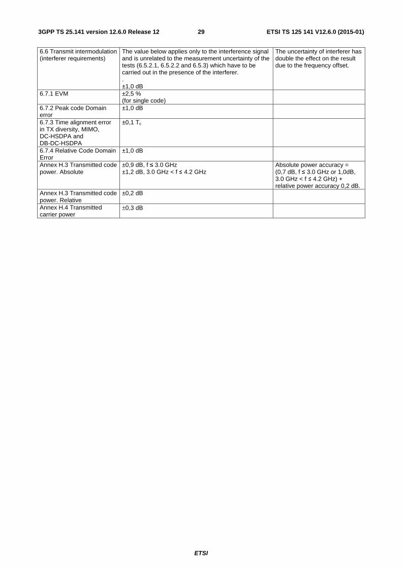
ETSI
ETSI TS 125 141 V12.6.0 (2015-01)293GPP TS 25.141 version 12.6.0 Release 12
6.6 Transmit intermodulation (interferer requirements)
The value below applies only to the interference signal and is unrelated to the measurement uncertainty of the tests (6.5.2.1, 6.5.2.2 and 6.5.3) which have to be carried out in the presence of the interferer. . ±1,0 dB
The uncertainty of interferer has double the effect on the result due to the frequency offset.
6.7.1 EVM ±2,5 % (for single code)
6.7.2 Peak code Domain error
±1,0 dB
6.7.3 Time alignment error in TX diversity, MIMO, DC-HSDPA and DB-DC-HSDPA
±0,1 Tc
6.7.4 Relative Code Domain Error
±1,0 dB
Annex H.3 Transmitted code power. Absolute
±0,9 dB, f ≤ 3.0 GHz ±1,2 dB, 3.0 GHz < f ≤ 4.2 GHz
Absolute power accuracy = (0,7 dB, f ≤ 3.0 GHz or 1,0dB, 3.0 GHz < f ≤ 4.2 GHz) + relative power accuracy 0,2 dB.
Annex H.3 Transmitted code power. Relative
±0,2 dB
Annex H.4 Transmitted carrier power
±0,3 dB
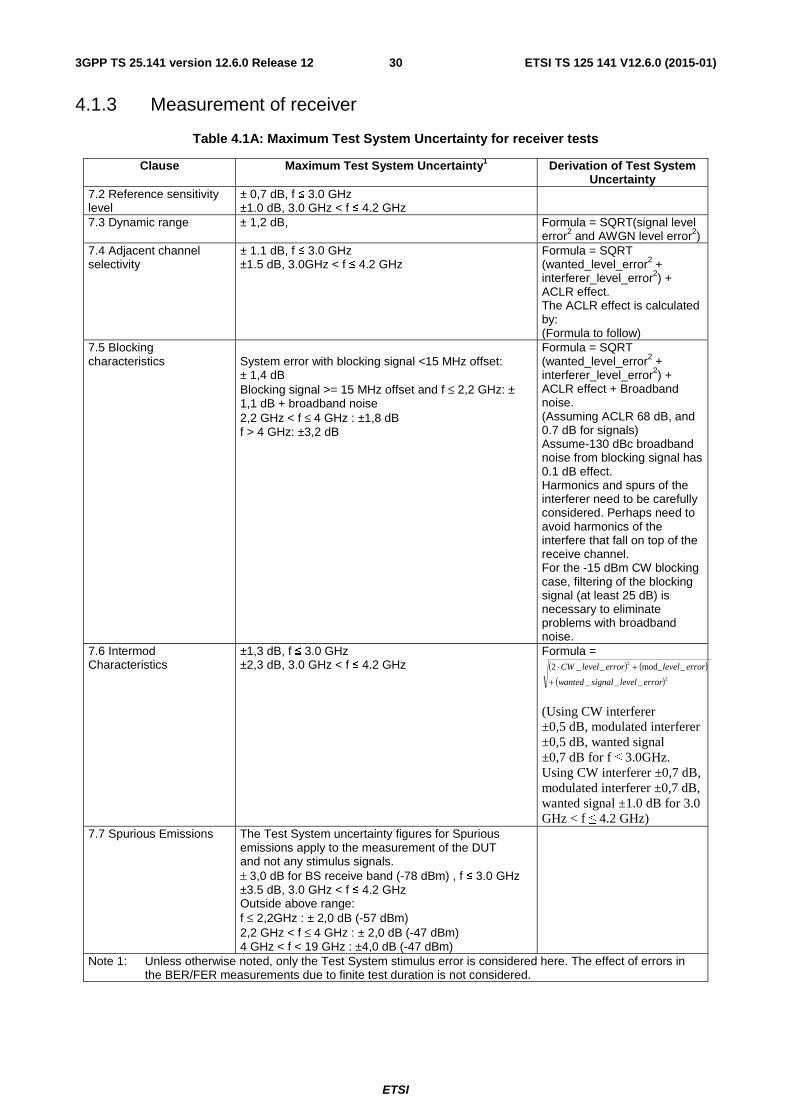
ETSI
ETSI TS 125 141 V12.6.0 (2015-01)303GPP TS 25.141 version 12.6.0 Release 12
4.1.3 Measurement of receiver
Table 4.1A: Maximum Test System Uncertainty for receiver tests
Clause Maximum Test System Uncertainty1 Derivation of Test System Uncertainty
7.2 Reference sensitivity level
± 0,7 dB, f ≤ 3.0 GHz ±1.0 dB, 3.0 GHz < f ≤ 4.2 GHz
7.3 Dynamic range ± 1,2 dB, Formula = SQRT(signal level error2 and AWGN level error2)
7.4 Adjacent channel selectivity
± 1.1 dB, f ≤ 3.0 GHz ±1.5 dB, 3.0GHz < f ≤ 4.2 GHz
Formula = SQRT (wanted_level_error2 + interferer_level_error2) + ACLR effect. The ACLR effect is calculated by: (Formula to follow)
7.5 Blocking characteristics
System error with blocking signal <15 MHz offset: ± 1,4 dB Blocking signal >= 15 MHz offset and f ≤ 2,2 GHz: ± 1,1 dB + broadband noise 2,2 GHz < f ≤ 4 GHz : ±1,8 dB f > 4 GHz: ±3,2 dB
Formula = SQRT (wanted_level_error2 + interferer_level_error2) + ACLR effect + Broadband noise. (Assuming ACLR 68 dB, and 0.7 dB for signals) Assume-130 dBc broadband noise from blocking signal has 0.1 dB effect. Harmonics and spurs of the interferer need to be carefully considered. Perhaps need to avoid harmonics of the interfere that fall on top of the receive channel. For the -15 dBm CW blocking case, filtering of the blocking signal (at least 25 dB) is necessary to eliminate problems with broadband noise.
7.6 Intermod Characteristics
±1,3 dB, f ≤ 3.0 GHz ±2,3 dB, 3.0 GHz < f ≤ 4.2 GHz
Formula = ( ) ( )
( )2
22
___
_mod___2
errorlevelsignalwanted
errorlevelerrorlevelCW
+
+⋅
(Using CW interferer ±0,5 dB, modulated interferer ±0,5 dB, wanted signal ±0,7 dB for f ≤ 3.0GHz. Using CW interferer ±0,7 dB, modulated interferer ±0,7 dB, wanted signal ±1.0 dB for 3.0 GHz < f ≤ 4.2 GHz)
7.7 Spurious Emissions The Test System uncertainty figures for Spurious emissions apply to the measurement of the DUT and not any stimulus signals. ± 3,0 dB for BS receive band (-78 dBm) , f ≤ 3.0 GHz ±3.5 dB, 3.0 GHz < f ≤ 4.2 GHz Outside above range: f ≤ 2,2GHz : ± 2,0 dB (-57 dBm) 2,2 GHz < f ≤ 4 GHz : ± 2,0 dB (-47 dBm) 4 GHz < f < 19 GHz : ±4,0 dB (-47 dBm)
Note 1: Unless otherwise noted, only the Test System stimulus error is considered here. The effect of errors in the BER/FER measurements due to finite test duration is not considered.

ETSI
ETSI TS 125 141 V12.6.0 (2015-01)313GPP TS 25.141 version 12.6.0 Release 12
4.1.4 Measurement of performance requirement
Table 4.1B: Maximum Test System Uncertainty for Performance Requirements
Clause Maximum Test System Uncertainty1
Derivation of Test System Uncertainty
8.2, Demodulation in static propagation condition
± 0,4 dB Wanted/AWGN: ±0,4 dB (relative uncertainty for Eb/N0) (AWGN: ±1 dB)
8.3, Demodulation of DCH in multiplath fading conditions
± 0,6 dB Fader: ± 0,5 dB Wanted/AWGN: ± 0,4 dB (relative) Combined relative uncertainty for Eb/N0: ±0,6 dB
8.4 Demodulation of DCH in moving propagation conditions
± 0,6 dB Fader: ± 0,5 dB Wanted/AWGN: ± 0,4 dB (relative) Combined relative uncertainty for Eb/N0: ±0,6 dB
8.5 Demodulation of DCH in birth/death propagation conditions
± 0,6 dB Fader: ± 0,5 dB Wanted/AWGN: ± 0,4 dB (relative) Combined relative uncertainty for Eb/N0: ±0,6 dB
8.5A Demodulation of DCH in high speed train conditions
± 0,6 dB Fader: ± 0,5 dB Wanted/AWGN: ± 0,4 dB (relative) Combined relative uncertainty for Eb/N0: ±0,6 dB
8.8.1 RACH preamble detection in static propagation conditions
± 0,4 dB Wanted/AWGN: ± 0,4 dB (relative uncertainty for Ec/N0) (AWGN: ±1 dB)
8.8.2 RACH preamble detection in multipath fading case 3
± 0,6 dB Fader: ± 0,5 dB Wanted/AWGN: ± 0,4 dB (relative) Combined relative uncertainty for Ec/N0: ±0,6 dB
8.8.2A RACH preamble detection in high speed train conditions
± 0,6 dB Fader: ± 0,5 dB Wanted/AWGN: ± 0,4 dB (relative) Combined relative uncertainty for Ec/N0: ±0,6 dB
8.8.3 Demodulation of RACH message in static propagation conditions
± 0,4 dB Wanted/AWGN: ±0,4 dB (relative uncertainty for Eb/N0) (AWGN: ±1 dB)
8.8.4 Demodulation of RACH message in multipath fading case 3
± 0,6 dB Fader: ±0,5 dB Wanted/AWGN: ±0,4 dB (relative) Combined relative uncertainty for Eb/N0: ±0,6 dB
8.8.5 Demodulation of RACH message in high speed train conditions
± 0,6 dB Fader: ±0,5 dB Wanted/AWGN: ±0,4 dB (relative) Combined relative uncertainty for Eb/N0: ±0,6 dB
8.11.1 ACK false alarm in static propagation conditions
± 0,4 dB Wanted/AWGN: ±0,4 dB (relative uncertainty for Ec/N0) (AWGN: ±1 dB)
8.11.2 ACK false alarm in multipath fading conditions
± 0,6 dB Fader: ±0,5 dB Wanted/AWGN: ±0,4 dB (relative) Combined relative uncertainty for Ec/N0: ±0,6 dB
8.11.3 ACK mis-detection in static propagation conditions
± 0,4 dB Wanted/AWGN: ±0,4 dB (relative uncertainty for Ec/N0) (AWGN: ±1 dB)
8.11.4 ACK mis-detection in multipath fading conditions
± 0,6 dB Fader: ±0,5 dB Wanted/AWGN: ±0,4 dB (relative) Combined relative uncertainty for Ec/N0: ±0,6 dB
8.11A.1 4C-HSDPA: ACK false alarm in static propagation conditions
± 0,4 dB Wanted/AWGN: ±0,4 dB (relative uncertainty for Ec/N0)
(AWGN: ±1 dB)

ETSI
ETSI TS 125 141 V12.6.0 (2015-01)323GPP TS 25.141 version 12.6.0 Release 12
8.11A.2 4C-HSDPA: ACK false alarm in multipath fading conditions
± 0,6 dB Fader: ±0,5 dB Wanted/AWGN: ±0,4 dB (relative)
Combined relative uncertainty for Ec/N0: ±0,6 dB
8.11A.3 4C-HSDPA: ACK mis-detection in static propagation conditions
± 0,4 dB Wanted/AWGN: ±0,4 dB (relative uncertainty for Ec/N0)
(AWGN: ±1 dB) 8.11A.4 4C-HSDPA: ACK mis-detection in multipath fading conditions
± 0,6 dB Fader: ±0,5 dB Wanted/AWGN: ±0,4 dB (relative)
Combined relative uncertainty for Ec/N0: ±0,6 dB
8.12 Demodulation of E-DPDCH in multipath fading conditions
± 0,6 dB Fader: ±0,5 dB Wanted/AWGN: ±0,4 dB (relative)
Combined relative uncertainty for Ec/N0: ±0,6 dB
8.13 Performance of signalling detection for E-DPCCH in multipath fading conditions
± 0,6 dB Fader: ±0,5 dB Wanted/AWGN: ±0,4 dB (relative)
Combined relative uncertainty for Ec/N0: ±0,6 dB
Note 1: Only the overall stimulus error is considered here. The effect of errors in the BER/FER measurements due to finite test duration is not considered.
4.2 Test Tolerances (informative) The Test Tolerances defined in this clause have been used to relax the Minimum Requirements in this specification to derive the Test Requirements.
The Test Tolerances are derived from Test System uncertainties, regulatory requirements and criticality to system performance. As a result, the Test Tolerances may sometimes be set to zero.
The test tolerances should not be modified for any reason e.g. to take account of commonly known test system errors (such as mismatch, cable loss, etc.)

ETSI
ETSI TS 125 141 V12.6.0 (2015-01)333GPP TS 25.141 version 12.6.0 Release 12
4.2.1 Transmitter
Table 4.1C: Test Tolerances for transmitter tests
Clause Test Tolerance1 f ≤ 3.0 GHz f > 3.0 GHz
6.2.1 Maximum Output Power 0,7 dB 1.0 dB 6.2.2 Primary CPICH Power accuracy 0,8 dB 1,1 dB 6.2.3 Secondary CPICH power offset accuracy 0,7 dB 1,0 dB 6.3 Frequency error 12 Hz 12 Hz 6.4.2 Power control steps 0,1 dB 0,1 dB 6.4.3 Power control dynamic range 1.1 dB 1.1 dB 6.4.4 Total power dynamic range 0,3 dB 0,3 dB 6.4.5 IPDL time mask 0,7 dB 0,7 dB 6.5.1 Occupied Bandwidth 0 kHz 0 kHz 6.5.2.1 Spectrum emission mask 1.5 dB3 1.8 dB 6.5.2.2 ACLR, CACLR 0,8 dB4 0,8 dB4 6.5.3 Spurious emissions 0 dB 0 dB 6.6 Transmit intermodulation (interferer requirements) 0 dB2 0 dB2 6.7.1 EVM 0 % 0 % 6.7.2 Peak code Domain error 1.0 dB 1.0 dB 6.7.3 Time alignment error in TX diversity, MIMO, DC-HSDPA and DB-DC-HSDPA
0,1 Tc 0,1 Tc
6.7.4 Relative Code Domain Error 1.0 dB 1.0 dB Annex H.3 Transmitted code power (absolute) 0,9 dB 1,2 dB Annex H.3 Transmitted code power (relative) 0,2 dB 0,2 dB Annex H.4 Transmitted carrier power 0,3 dB 0,3 dB Note 1: Unless otherwise stated, The Test Tolerances are applied to the DUT Minimum Requirement. See Annex F. Note 2: The Test Tolerance is applied to the stimulus signal(s). See Annex F. Note 3: 0 dB test tolerance for the additional Band II, IV, V, X, XII, XIII and XIV requirements. Note 4: 1.5 dB for absolute ACLR limit for Home BS for f≤ 3.0 GHz and 1.8 dB for 3.0 GHz < f ≤ 4.2 GHz.
4.2.2 Receiver
Table 4.1D: Test Tolerances for receiver tests
Clause Test Tolerance1 f ≤ 3.0 GHz f > 3.0 GHz
7.2 Reference sensitivity level 0,7 dB 1,0 dB 7.3 Dynamic range 1,2 dB 1,2 dB 7.4 Adjacent channel selectivity 0 dB 0 dB 7.5 Blocking characteristics 0 dB 0 dB 7.6 Intermod Characteristics 0 dB 0 dB 7.7 Spurious Emissions 0 dB
2 0 dB
2
Note 1: Unless otherwise stated, the Test Tolerances are applied to the stimulus signal(s). See Annex F. Note 2: The Test Tolerance is applied to the DUT Minimum Requirement. See Annex F.

ETSI
ETSI TS 125 141 V12.6.0 (2015-01)343GPP TS 25.141 version 12.6.0 Release 12
4.2.3 Performance requirement
Table 4.1E: Test Tolerances for Performance Requirements
Clause Test Tolerance1 8.2, Demodulation in static propagation condtion 0,4 dB 8.3, Demodulation of DCH in multiplath fading conditons 0,6 dB 8.4 Demodulation of DCH in moving propagation conditions 0,6 dB 8.5 Demodulation of DCH in birth/death propagation conditions 0,6 dB 8.5A Demodulation of DCH in high speed train conditions 0,6 dB 8.8.1 RACH preamble detection in static propagation conditions 0,4 dB 8.8.2 RACH preamble detection in multipath fading case 3 0,6 dB 8.8.2A RACH preamble detection in high speed train conditions 0,6 dB 8.8.3 Demodulation of RACH message in static propagation conditions
0,4 dB
8.8.4 Demodulation of RACH message in multipath fading case 3 0,6 dB 8.8.5 Demodulation of RACH message in high speed train conditions 0,6 dB 8.11.1 ACK false alarm in static propagation conditions 0,4 dB 8.11.2 ACK false alarm in multipath fading conditions 0,6 dB 8.11.3 ACK mis-detection in static propagation conditions 0,4 dB 8.11.4 ACK mis-detection in multipath fading conditions 0,6 dB 8.11A.1 4C-HSDPA: ACK false alarm in static propagation conditions
0,4 dB
8.11A.2 4C-HSDPA: ACK false alarm in multipath fading conditions 0,6 dB 8.11A.3 4C-HSDPA: ACK mis-detection in static propagation conditions
0,4 dB
8.11A.4 4C-HSDPA: ACK mis-detection in multipath fading conditions
0,6 dB
8.12 Demodulation of E-DPDCH in multipath fading conditions 0,6 dB 8.12A Demodulation of E-DPDCH and S-E-DPDCH in multipath fading conditions for UL MIMO
0,6 dB
8.13 Performance of signalling detection for E-DPCCH in multipath fading conditions
0,6 dB
NOTE 1: Unless otherwise stated, the Test Tolerances are applied to the stimulus signal(s). See Annex F.
4.2.4 RRM measurements
The following tolerances refer to the requirements of 25.133.
tbd
4.3 Interpretation of measurement results The measurement results returned by the Test System are compared - without any modification - against the Test Requirements as defined by the shared risk principle.
The Shared Risk principle is defined in ITU-R M.1545 [17].
The actual measurement uncertainty of the Test System for the measurement of each parameter shall be included in the test report.
The recorded value for the Test System uncertainty shall be, for each measurement, equal to or lower than the appropriate figure in clause 4.1 of this specification.
If the Test System for a test is known to have a measurement uncertainty greater than that specified in clause 4.1, it is still permitted to use this apparatus provided that an adjustment is made as follows.
Any additional uncertainty in the Test System over and above that specified in clause 4.1 shall be used to tighten the Test Requirement-making the test harder to pass. (For some tests e.g. receiver tests, this may require modification of stimulus signals). This procedure (defined in Annex F) will ensure that a Test System not compliant with clause 4.1does

ETSI
ETSI TS 125 141 V12.6.0 (2015-01)353GPP TS 25.141 version 12.6.0 Release 12
not increase the chance of passing a device under test where that device would otherwise have failed the test if a Test System compliant with clause 4.1 had been used.
4.3A Base station classes The requirements in the present document apply to Wide Area Base Stations, Medium Range Base Stations, Local Area Base Stations and Home Base Stations unless otherwise stated.
Wide Area Base Stations are characterised by requirements derived from Macro Cell scenarios with a BS to UE minimum coupling loss equals to 70 dB. The Wide Area Base Station class has the same requirements as the base station for General Purpose application in Release 99, 4 and 5.
Medium Range Base Stations are characterised by requirements derived from Micro Cell scenarios with a BS to UE minimum coupling loss equals to 53 dB.
Local Area Base Stations are characterised by requirements derived from Pico Cell scenarios with a BS to UE minimum coupling loss equals to 45 dB.
Home Base Stations are characterised by requirements derived from Femto Cell scenarios.
The manufacturer shall declare the intended class of the BS under test.
4.4 Test environments For each test in the present document, the environmental conditions under which the BS is to be tested are defined.
4.4.1 Normal test environment
When a normal test environment is specified for a test, the test should be performed within the minimum and maximum limits of the conditions stated in table 4.2.
Table 4.2: Limits of conditions for Normal Test Environment
Condition Minimum Maximum Barometric pressure 86 kPa 106 kPa Temperature 15°C 30°C Relative Humidity 20 % 85 % Power supply Nominal, as declared by the manufacturer Vibration Negligible
The ranges of barometric pressure, temperature and humidity represent the maximum variation expected in the uncontrolled environment of a test laboratory. If it is not possible to maintain these parameters within the specified limits, the actual values shall be recorded in the test report.
NOTE: This may, for instance, be the case for measurements of radiated emissions performed on an open field test site.
4.4.2 Extreme test environment
The manufacturer shall declare one of the following:
1) the equipment class for the equipment under test, as defined in the IEC 60 721-3-3 [6];
2) the equipment class for the equipment under test, as defined in the IEC 60 721-3-4 [7];
3) the equipment that dose not comply to the mentioned classes, the relevant classes from IEC 60 721 documentation for Temperature, Humidity and Vibration shall be declared.
NOTE: Reduced functionality for conditions that fall out side of the standard operational conditions are not tested in the present document. These may be stated and tested separately.

ETSI
ETSI TS 125 141 V12.6.0 (2015-01)363GPP TS 25.141 version 12.6.0 Release 12
4.4.2.1 Extreme temperature
When an extreme temperature test environment is specified for a test, the test shall be performed at the standard minimum and maximum operating temperatures defined by the manufacturer's declaration for the equipment under test.
Minimum temperature:
The test shall be performed with the environment test equipment and methods including the required environmental phenomena into the equipment, conforming to the test procedure of IEC 60 068-2-1 [8].
Maximum temperature:
The test shall be performed with the environmental test equipment and methods including the required environmental phenomena into the equipment, conforming to the test procedure of IEC 60 068-2-2 [9].
NOTE: It is recommended that the equipment is made fully operational prior to the equipment being taken to its lower operating temperature.
4.4.3 Vibration
When vibration conditions are specified for a test, the test shall be performed while the equipment is subjected to a vibration sequence as defined by the manufacturer"s declaration for the equipment under test. This shall use the environmental test equipment and methods of inducing the required environmental phenomena in to the equipment, conforming to the test procedure of IEC 60 068-2-6 [10]. Other environmental conditions shall be within the ranges specified in clause 4.4.1.
NOTE: The higher levels of vibration may induce undue physical stress in to equipment after a prolonged series of tests. The testing body should only vibrate the equipment during the RF measurement process.
4.4.4 Power supply
When extreme power supply conditions are specified for a test, the test shall be performed at the standard upper and lower limits of operating voltage defined by manufacturer's declaration for the equipment under test.
Upper voltage limit:
The equipment shall be supplied with a voltage equal to the upper limit declared by the manufacturer (as measured at the input terminals to the equipment). The tests shall be carried out at the steady state minimum and maximum temperature limits declared by the manufacturer for the equipment, to the methods described in IEC 60 068-2-1 [8] Test Ab/Ad and IEC 60 068-2-2 [9] Test Bb/Bd: Dry Heat.
Lower voltage limit:
The equipment shall be supplied with a voltage equal to the lower limit declared by the manufacturer (as measured at the input terminals to the equipment). The tests shall be carried out at the steady state minimum and maximum temperature limits declared by the manufacturer for the equipment, to the methods described in IEC 60 068-2-1 [8] Test Ab/Ad and IEC 60 068-2-2 [9] Test Bb/Bd: Dry Heat.
4.4.5 Definition of Additive White Gaussian Noise (AWGN) Interferer
The minimum bandwidth of the AWGN interferer shall be 1.5 times chip rate of the radio access mode. (e.g. 5.76 MHz for a chip rate of 3.84 Mcps). The flatness across this minimum bandwidth shall be less than ±0.5 dB and the peak to average ratio at a probability of 0.001% shall exceed 10 dB.
4.5 Selection of configurations for testing Most tests in the present document are only performed for a subset of the possible combinations of test conditions. For instance:
- not all transceivers in the configuration may be specified to be tested;
- only one RF channel may be specified to be tested;

ETSI
ETSI TS 125 141 V12.6.0 (2015-01)373GPP TS 25.141 version 12.6.0 Release 12
- only one timeslot may be specified to be tested.
When a test is performed by a test laboratory, the choice of which combinations are to be tested shall be specified by the laboratory. The laboratory may consult with operators, the manufacturer or other bodies.
When a test is performed by a manufacturer, the choice of which combinations are to be tested may be specified by an operator.
4.6 BS Configurations
4.6.1 Receiver diversity
For the tests in clause 7 of the present document, the requirement applies at each receiver antenna connector for receivers with antenna diversity.
Receiver requirements are tested at the antenna connector, with the remaining receiver(s) disabled or their antenna connector(s) being terminated. If the manufacturer has declared the receiver paths to be equivalent, it is sufficient to apply the specified test signal at any one of the receiver antenna connectors.
For a multi-band BS, multi-band tests for ACS, blocking and intermodulation are performed with the interferer(s) applied to each antenna connector mapped to the receiver for the wanted signal(s), however only to one antenna at a time. Antenna connectors to which no signals are applied are terminated.
4.6.2 Duplexers
The requirements of the present document shall be met with a duplexer fitted, if a duplexer is supplied as part of the BS. If the duplexer is supplied as an option by the manufacturer, sufficient tests should be repeated with and without the duplexer fitted to verify that the BS meets the requirements of the present document in both cases.
The following tests should be performed with the duplexer fitted, and without it fitted if this is an option:
1) clause 6.2.1, base station maximum output power, for the highest static power step only, if this is measured at the antenna connector;
2) clause 6.5, output RF spectrum emissions; outside the BS transmit band;
3) clause 6.5.3.4.3, protection of the BS receiver;
4) clause 6.6, transmit intermodulation; for the testing of conformance, the carrier frequencies should be selected to minimize intermodulation products from the transmitters falling in receive channels.
The remaining tests may be performed with or without the duplexer fitted.
NOTE 1: When performing receiver tests with a duplexer fitted, it is important to ensure that the output from the transmitters does not affect the test apparatus. This can be achieved using a combination of attenuators, isolators and filters.
NOTE 2: When duplexers are used, intermodulation products will be generated, not only in the duplexer but also in the antenna system. The intermodulation products generated in the antenna system are not controlled by 3GPP specifications, and may degrade during operation (e.g. due to moisture ingress). Therefore, to ensure continued satisfactory operation of a BS, an operator will normally select ARFCNs to minimize intermodulation products falling on receive channels. For testing of complete conformance, an operator may specify the ARFCNs to be used.
4.6.3 Power supply options
If the BS is supplied with a number of different power supply configurations, it may not be necessary to test RF parameters for each of the power supply options, provided that it can be demonstrated that the range of conditions over which the equipment is tested is at least as great as the range of conditions due to any of the power supply configurations.
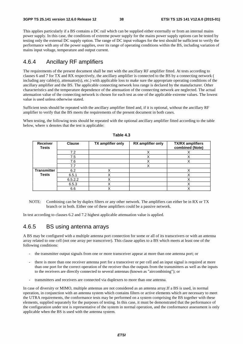
ETSI
ETSI TS 125 141 V12.6.0 (2015-01)383GPP TS 25.141 version 12.6.0 Release 12
This applies particularly if a BS contains a DC rail which can be supplied either externally or from an internal mains power supply. In this case, the conditions of extreme power supply for the mains power supply options can be tested by testing only the external DC supply option. The range of DC input voltages for the test should be sufficient to verify the performance with any of the power supplies, over its range of operating conditions within the BS, including variation of mains input voltage, temperature and output current.
4.6.4 Ancillary RF amplifiers
The requirements of the present document shall be met with the ancillary RF amplifier fitted. At tests according to clauses 6 and 7 for TX and RX respectively, the ancillary amplifier is connected to the BS by a connecting network ( including any cable(s), attenuator(s), etc.) with applicable loss to make sure the appropriate operating conditions of the ancillary amplifier and the BS. The applicable connecting network loss range is declared by the manufacturer. Other characteristics and the temperature dependence of the attenuation of the connecting network are neglected. The actual attenuation value of the connecting network is chosen for each test as one of the applicable extreme values. The lowest value is used unless otherwise stated.
Sufficient tests should be repeated with the ancillary amplifier fitted and, if it is optional, without the ancillary RF amplifier to verify that the BS meets the requirements of the present document in both cases.
When testing, the following tests should be repeated with the optional ancillary amplifier fitted according to the table below, where x denotes that the test is applicable:
Table 4.3
Receiver Tests
Clause TX amplifier only RX amplifier only TX/RX amplifiers combined (Note)
7.2 X X 7.5 X X 7.6 X X 7.7 X
Transmitter Tests
6.2 X X 6.5.1 X X
6.5.2.2 X X 6.5.3 X X 6.6 X X
NOTE: Combining can be by duplex filters or any other network. The amplifiers can either be in RX or TX branch or in both. Either one of these amplifiers could be a passive network.
In test according to clauses 6.2 and 7.2 highest applicable attenuation value is applied.
4.6.5 BS using antenna arrays
A BS may be configured with a multiple antenna port connection for some or all of its transceivers or with an antenna array related to one cell (not one array per transceiver). This clause applies to a BS which meets at least one of the following conditions:
- the transmitter output signals from one or more transceiver appear at more than one antenna port; or
- there is more than one receiver antenna port for a transceiver or per cell and an input signal is required at more than one port for the correct operation of the receiver thus the outputs from the transmitters as well as the inputs to the receivers are directly connected to several antennas (known as "aircombining"); or
- transmitters and receivers are connected via duplexers to more than one antenna.
In case of diversity or MIMO, multiple antennas are not considered as an antenna array.If a BS is used, in normal operation, in conjunction with an antenna system which contains filters or active elements which are necessary to meet the UTRA requirements, the conformance tests may be performed on a system comprising the BS together with these elements, supplied separately for the purposes of testing. In this case, it must be demonstrated that the performance of the configuration under test is representative of the system in normal operation, and the conformance assessment is only applicable when the BS is used with the antenna system.

ETSI
ETSI TS 125 141 V12.6.0 (2015-01)393GPP TS 25.141 version 12.6.0 Release 12
For conformance testing of such a BS, the following procedure may be used.
4.6.5.1 Receiver tests
For each test, the test signals applied to the receiver antenna connectors shall be such that the sum of the powers of the signals applied equals the power of the test signal(s) specified in the test.
An example of a suitable test set-up is shown in figure 4.1.
Splitting network
Base
Station
Rx antenna interface
Test input port
P
Pi Ps = sum(Pi), where Ps is the required input power specified
Figure 4.1: Receiver test set-up
For spurious emissions from the receiver antenna connector, the test may be performed separately for each receiver antenna connector.
4.6.5.2 Transmitter tests
For each test, the test signals applied to the transmitter antenna connectors (Pi) shall be such that the sum of the powers of the signals applied equals the power of the test signal(s) (Ps) specified in the test. This may be assessed by separately measuring the signals emitted by each antenna connector and summing the results, or by combining the signals and performing a single measurement. The characteristics (e.g. amplitude and phase) of the combining network should be such that the power of the combined signal is maximised.
An example of a suitable test set-up is shown in figure 4.2.
Combining
network
Base
Station
Tx antenna interface
Test output port
Ps
Pi
Ps = sum(Pi), where Ps is the required output power specified
Figure 4.2: Transmitter test set-up
For Intermodulation attenuation, the test may be performed separately for each transmitter antenna connector.
4.6.6 Transmit diversity and MIMO transmission
Unless otherwise stated, for the tests in clause 6 of the present document, the requirement applies for each transmitter antenna connector in case of transmit diversity, DB-DC-HSDPA or MIMO transmission.
Transmitter requirements are tested at the antenna connector, with the remaining antenna connector(s) being terminated. If the manufacturer has declared the transmitter paths to be equivalent, it is sufficient to measure the signal at any one of the transmitter antenna connectors.

ETSI
ETSI TS 125 141 V12.6.0 (2015-01)403GPP TS 25.141 version 12.6.0 Release 12
4.6.7 BS with integrated Iuant BS modem
Unless otherwise stated, for the tests in the present document, the integrated Iuant BS modem shall be switched off. Spurious emissions according to clauses 6.5.3 and 7.7 shall be measured only for frequencies above 20MHz with the integrated Iuant BS modem switched on.
4.6.8 BS with Virtual Antenna Mapping
A BS may be configured with virtual antenna mapping (VAM) as shown as example in Figure 4.3 for MIMO mode with two transmit antennas. The purpose of VAM is to achieve the goal of power balancing of physical channels across the multiple physical antennas when MIMO mode with two or four transmit antennas is is deployed in the downlink. Since the non-MIMO channels are transmitted only via virtual antenna 1, the transmission powers are not balanced at point a. The VAM function transforms the input signals at point a to output signals at point b such that the transmission powers are balanced.
In the following some characteristics of VAM are described in the context of MIMO mode with two transmit antennas. Similar characteristics apply also when VAM is implemented in the context of MIMO mode with four transmit antennas.
Some characteristics of VAM are as follows:
- The VAM can be represented by a unitary matrix ⎥⎦
⎤⎢⎣
⎡
42
31
ss
ss
- The same pair of weights (s1,s2) are applied to each physical channel that appears at virtual antenna port 1
- The same pair of weights (s3,s4) are applied to each physical channel that appears at virtual antenna port 2
- The VAM weights (s1,s2,s3,s4) should satisfy the following condition for MIMO and non-MIMO channels :
12
4
2
2
2
3
2
1 =+=+ ssss
- Power balancing at the output of VAM is achieved by setting 2
4
2
3
2
2
2
1 and ssss ==
- The VAM function is implemented in the digital domain prior to digital to analog conversion.
Virtual Antenna
Mapping
(VAM)
X
X
X
X
P- CPICH
S- CPICH
HS- DSCH2
HS- DSCH1
Other channels
Virtual antenna 1
Virtual antenna 2
Physical antenna 1
Physical antenna 2
a b
a = powers unbalanced between antennas
b = powers balanced between antennas
Figure 4.3: Example of VAM for MIMO mode with two transmit antennas.
If NodeB manufacturer declares the implementation of a Virtual Antenna Mapping (VAM), then the S-CPICH power accuracy test in section 6.2.3 will not be performed.

ETSI
ETSI TS 125 141 V12.6.0 (2015-01)413GPP TS 25.141 version 12.6.0 Release 12
4.7 Regional requirements Some requirements in TS 25.141 may only apply in certain regions. Table 4.4 lists all requirements that may be applied differently in different regions.

ETSI
ETSI TS 125 141 V12.6.0 (2015-01)423GPP TS 25.141 version 12.6.0 Release 12
Table 4.4: List of regional requirements
Clause number
Requirement Comments
3.4.1 Frequency bands Some bands may be applied regionally. 3.4.2 Tx-Rx Frequency Separation The requirement is applied according to what
frequency bands in clause 3.4.1 that are supported by the BS.
3.5 Channel arrangement The requirement is applied according to what frequency bands in clause 3.4.1 that are supported by the BS.
6.2.1.2 Base station output power In certain regions, the minimum requirement for normal conditions may apply also for some conditions outside the ranges defined for the Normal test environment in clause 4.4.1.
6.5.2.1 Spectrum emission mask The mask specified may be mandatory in certain regions. In other regions this mask may not be applied. Additional spectrum protection requirements may apply regionally.
6.5.2.2 Adjacent Channel Leakage power Ratio
In Japan, the requirement depicted in the note of Table 6.23 shall be applied.
6.5.3.7.1 Spurious emissions (Category A) These requirements shall be met in cases where Category A limits for spurious emissions, as defined in ITU-R Recommendation SM.329 [4], are applied.
6.5.3.7.2 Spurious emissions (Category B) These requirements shall be met in cases where Category B limits for spurious emissions, as defined in ITU-R Recommendation SM.329 [4], are applied.
6.5.3.7.4 Co-existence with other systems in the same geographical area
These requirements may apply in geographic areas in which both UTRA FDD and GSM900, DCS1800, PCS1900, GSM850 and/or UTRA FDD operating in another frequency band are deployed.
6.5.3.7.5 Co-existence with co-located and co-sited base stations
These requirements may be applied for the protection of other BS receivers when GSM900, DCS1800, PCS1900, GSM850 and/or FDD BS operating in another frequency band are co-located with a UTRA FDD BS.
6.5.3.7.6 Co-existence with PHS This requirement may be applied for the protection of PHS in geographic areas in which both PHS and UTRA FDD are deployed.
6.5.3.7.7 Co-.existence with services in adjacent frequency bands
This requirement may be applied for the protection in bands adjacent to the downlink band as defined in clause 3.4.1 in geographic areas in which both an adjacent band service and UTRA FDD are deployed.
6.5.3.7.8.1 Co-existence with UTRA TDD - Operation in the same geographic area
This requirement may be applied to geographic areas in which both UTRA-TDD and UTRA-FDD are deployed.
6.5.3.7.8.2 Co-existence with UTRA TDD - Co-located base stations
This requirement may be applied for the protection of UTRA-TDD BS receivers when UTRA-TDD BS and UTRA FDD BS are co-located.
6.5.3.7.9 Protection of public safety operations
This requirement shall be applied to BS operating in Bands XIII and XIV to ensure that appropriate interference protection is provided to 700 MHz public safety operations.
7.5 Blocking characteristic The requirement is applied according to what frequency bands in clause 3.4.1 that are supported by the BS.
7.5 Blocking characteristics This requirement may be applied for the protection of UTRA FDD BS receivers when UTRA FDD BS and GSM 900, GSM850, PCS 1900 and BS operating in the /DCS1800 band (GSM or UTRA) are co-located.
7.6 Intermodulation characteristics The requirement is applied according to what frequency bands in clause 3.4.1 that are supported by the BS.
7.7 Spurious emissions The requirement is applied according to what frequency bands in clause 3.4.1 that are supported by the BS.

ETSI
ETSI TS 125 141 V12.6.0 (2015-01)433GPP TS 25.141 version 12.6.0 Release 12
Base station classes* Only requirements for Wide Area (General Purpose), Medium Range and Local Area Base Stations are applicable in Japan.
Note *: Base station classes,: This regional requirement should be reviewed to check its necessity every TSG RAN meeting.
4.8 Specified frequency range The manufacturer shall declare:
- which of the frequency bands defined in sub-clause 3.4 are supported by the BS.
- the frequency range within the above frequency band(s) supported by the BS.
Many tests in this TS are performed with appropriate frequencies in the bottom, middle and top of the frequency range supported by the BS. These are denoted as RF channels B (bottom), M (middle) and T (top).
Unless otherwise stated, the test shall be performed with a single carrier at each of the RF channels B, M and T.
When a test is performed by a test laboratory, the UARFCNs to be used for RF channels B, M and T shall be specified by the laboratory. The laboratory may consult with operators, the manufacturer or other bodies.
When a test is performed by a manufacturer, the UARFCNs to be used for RF channels B, M and T may be specified by an operator.
4.8.1 RF bandwidth position for non-single carrier testing
Many tests in this TS are performed with the maximum BS RF bandwidth located at the bottom, middle and top of the supported frequency range in each operating band. These are denoted as BRFBW(bottom), MRFBW (middle) and TRFBW (top).
Unless otherwise stated, the test shall be performed at BRFBW, MRFBW and TRFBW defined as following:
- BRFBW: Maximum BS RF bandwidth located at the bottom of the supported frequency range in each operating band;
- MRFBW: Maximum BS RF bandwidth located in the middle of the supported frequency range in each operating band;
- TRFBW: maximum BS RF bandwidth located at the top of the supported frequency range in each operating band.
For BS capable of dual-band operation, unless otherwise stated, the test shall be performed at BRFBW_T"RFBW and B"RFBW_TRFBW defined as following:
BRFBW_ T"RFBW: the RF bandwidths located at the bottom of the supported frequency range in the lower operating band and at the highest possible simultaneous frequency position, within the maximum radio bandwidth, in the upper operating band.
B"RFBW_TRFBW: the RF bandwidths located at the top of the supported frequency range in the upper operating band and at the lowest possible simultaneous frequency position, within the maximum radio bandwidth, in the lower operating band.
NOTE: BRFBW_T"RFBW = B"RFBW_TRFBW = BRFBW_TRFBW when the declared maximum radio bandwidth spans both operating bands. BRFBW_TRFBW means the RF bandwidths are located at the bottom of the supported frequency range in the lower operating band and at the top of the supported frequency range in the upper operating band.

ETSI
ETSI TS 125 141 V12.6.0 (2015-01)443GPP TS 25.141 version 12.6.0 Release 12
When a test is performed by a test laboratory, the position of BRFBW, MRFBW and TRFBW in each supported operating band, as well as the position of BRFBW_T"RFBW and B"RFBW_TRFBW in the supported operating band combinations, shall be specified by the laboratory. The laboratory may consult with operators, the manufacturer or other bodies.
4.9 Applicability of requirements For BS that is UTRA (single-RAT) capable only, the requirements in the present document are applicable and additional conformance to TS 37.141 [16] is optional. For a BS additionally conforming to TS 37.141 [16], conformance to some of the RF requirements in the present document can be demonstrated through the corresponding requirements in TS 37.141 [16] as listed in Table 4.5
Table 4.5: Alternative RF test requirements for a BS additionally conforming to TS 37.141 [16]
RF requirement Clause in the present document
Alternative clause in TS 37.141 [16]
Base station output power 6.2.1.5 6.2.1 6.2.2
Unwanted emissions Spectrum emission mask 6.5.2.1.5 6.6.2.5 (except for
6.6.2.5.3 and 6.6.2.5.4) Transmitter spurious emissions 6.5.3.7 (except for
6.5.3.7.9) 6.6.1.5 (except for
6.6.1.5.3) Transmitter intermodulation 6.6.5 6.7.5.1 Narrowband blocking 7.5.5 7.4.5.2 Blocking 7.5.5 7.4. 5.1 Out-of-band blocking 7.5.5 7.5. 5.1 Co-location with other base stations 7.5.5 7.5. 5.2 Receiver spurious emissions 7.7.5 7.6. 5.1 Intermodulation 7.6.5 7.7. 5.1 Narrowband intermodulation 7.6.5 7.7. 5.2
4.10 Requirements for contiguous and non-contiguous spectrum A spectrum allocation where the BS operates can either be contiguous or non-contiguous. Unless otherwise stated, the requirements in the present specification apply for BS configured for both contiguous spectrum operation and non-contiguous spectrum operation.
For BS operation in non-contiguous spectrum, some requirements apply also inside the sub-block gaps. For each such requirement, it is stated how the limits apply relative to the sub-block edges.
4.11 Manufacturer"s declarations of regional and optional requirements
4.11.1 Operating band and frequency range
Manufacturer declarations related to supported frequency band(s) and frequency ranges are contained in section 4.8. Requirements for other operating bands and frequency ranges need not be tested.
Some tests are performed with the maximum BS RF bandwidth. The manufacturer shall declare that the requirements are also fulfilled for all other supported BS RF bandwidths which are not tested.
4.11.2 Spurious emissions category
The manufacturer shall declare one of the following:
a) The BS is tested against Category A limits for spurious emissions, as defined in ITU-R Recommendation SM.329 [4]. In this case:
ETSI
ETSI TS 125 141 V12.6.0 (2015-01)453GPP TS 25.141 version 12.6.0 Release 12
- conformance with the spurious emissions requirements in clause 6.5.3.7.1 is mandatory, and the requirements specified in clause 6.5.3.7.2 need not be tested.
b) The BS is tested against Category B limits for spurious emissions, as defined in ITU-R Recommendation SM.329 [4]. In this case:
- conformance with the spurious emissions requirements in clause 6.5.3.7.2 is mandatory, and the requirements specified in clause 6.5.3.7.1 need not be tested.
4.11.3 Additional out of band emissions
For a BS declared to support Band XX and to operate in geographic areas within the CEPT in which frequencies are allocated to broadcasting (DTT) service, the manufacturer shall additionally declare the following quantities associated with the applicable test conditions of Table 6.21F and information in annex D of [1] :
PEM,N Declared emission level for channel N
P10MHz Maximum output Power in 10 MHz
4.11.4 Co-existence with other systems
The manufacturer shall declare whether the BS under test is intended to operate in geographic areas where one or more of the systems GSM850, GSM900, DCS1800, PCS1900, UTRA FDD, UTRA TDD, E-UTRA and/or PHS operating in another band are deployed. If this is the case, compliance with the applicable test requirement for spurious emissions specified in clauses 6.5.3.7.4, 6.5.3.7.6, 6.5.3.7.7 and 6.5.3.7.9 shall be tested.
4.11.5 Co-location with other base stations
The manufacturer shall declare whether the BS under test is intended to operate co-located with base stations of one or more of the systems GSM850, GSM900, DCS1800, PCS1900, UTRA FDD, UTRA TDD and/or E-UTRA operating in another band. If this is the case,
- compliance with the applicable test requirement for spurious emissions specified in clause 6.5.3.7.5 shall be tested.
- compliance with the applicable test requirement for receiver blocking specified in clause 7.5 shall be tested.
4.11.6 Manufacturer's declarations of supported RF configurations
The manufacturer shall declare the intended class of the BS under test, as specified in subclause 4.3A.
The manufacturer shall declare which operational configurations the BS supports by declaring the following parameters:
- Support of the BS in non-contiguous spectrum operation. If the BS does not support non-contiguous spectrum operation the parameters for non-contiguous spectrum operation below shall not be declared.
- The supported operating bands defined in subclause 3.4;
- The frequency range within the above operating band(s) supported by the BS;
- The Maximum Base Station RF bandwidth supported by a BS within each operating band;
• for contiguous spectrum operation
• for non-contiguous spectrum operation
- The supported operating configurations (multi-carrier and/or single carrier) within each operating band.
- The rated output power per carrier (PRAT);
• for contiguous spectrum operation

ETSI
ETSI TS 125 141 V12.6.0 (2015-01)463GPP TS 25.141 version 12.6.0 Release 12
• for non-contiguous spectrum operation
NOTE: Different rated output powers may be declared for different operating configurations.
- The rated total output power (Prated,t) as a sum of all carriers;
• for contiguous spectrum operation
• for non-contiguous spectrum operation
- Maximum number of supported carriers within each band;
• for contiguous spectrum operation
• for non-contiguous spectrum operation
- Total number of supported carriers
If the rated total output power and total number of supported carriers are not simultaneously supported, the manufacturer shall declare the following additional parameters:
• The reduced number of supported carriers at the rated total output power.
• The reduced total output power at the maximum number of supported carriers.
- Whether virtual antenna mapping (VAM) as described in 4.6.8 is implemented in the BS under test.
- Primary CPICH code domain power, in the case of MIMO or transmit diversity.
For BS capable of multi-band operation, the parameters above shall be declared for each supported operating band, in which declarations of the maximum Base Station RF bandwidth, the rated output power per carrier, the rated total output power and maximum number of supported carriers are applied for single-band operation only. In addition the manufacturer shall declare the following additional parameters for BS capable of multi-band operation:
- Supported operating band combinations of the BS
- Supported operating band(s) of each antenna connector
- Support of multi-band transmitter and/or multi-band receiver, including mapping to antenna connector(s)
- Total number of supported carriers for the declared band combinations of the BS
- Maximum number of supported carriers per band in multi-band operation
- Total RF bandwidth of transmitter and receiver for the declared band combinations of the BS
- Maximum RF bandwidth of each supported operating band in multi-band operation
- Maximum radio bandwidth in transmit and receive direction for the declared band combinations of the BS
- Any other limitations under simultaneous operation in the declared band combinations of the BS which have any impact on the test configuration generation
- Total output power as a sum over all supported operating bands in the declared band combinations of the BS
- Maximum supported power difference between any two carriers in any two different supported operating bands
- The rated output power per carrier in multi-band operation
- Rated total output power of each supported operating band in multi-band operation
4.12 Test configuration for multi-carrier operations The test configurations shall be constructed using the methods defined below, subject to the parameters declared by the manufacturer for the supported RF configurations as listed in subclause 4.11.6. The test configurations to use for conformance testing are defined for each supported RF configuration in subclause 4.12.4

ETSI
ETSI TS 125 141 V12.6.0 (2015-01)473GPP TS 25.141 version 12.6.0 Release 12
The applicable Test Models for generation of the carrier transmit test signal are defined in subclause 6.1.1.
4.12.1 UTC1: Contiguous spectrum operation test configuration
The purpose of the UTC1 is to test both BS transmitter and receiver requirements. UTC1 should be constructed using the following method:
- The RF bandwidth shall be the declared maximum BS RF bandwidth for contiguous operation.
- Place one UTRA FDD carrier adjacent to the upper RF bandwidth edge and one UTRA FDD carrier adjacent to the lower RF bandwidth edge. The specified FOffset shall apply.
- For transmitter tests, alternately place a UTRA FDD carrier adjacent to the already placed carriers at the low and high edge of the RF bandwidth until there is no more space to fit a carrier or the BS does not support more carriers. The nominal carrier spacing defined in subclause 3.5.1 shall apply.
- The carrier(s) may be shifted maximum 100 kHz towards lower frequencies for BRFBW and MRFBW and towards higher frequencies for TRFBW to align with the channel raster.
4.12.1.1 UTC1 power allocation
Set the power of each carrier to the same level so that the sum of the carrier powers equals the rated total output power (Prated,t) according to the manufacturer"s declaration in sub clause 4.11.6.
4.12.2 UTC2: Non-contiguous spectrum operation test configuration
The purpose of the UTC2 is to test both the BS transmitter and receiver requirements. UTC2 should be constructed using the following method:
- The RF bandwidth shall be the maximum BS RF bandwidth for non-contiguous operation. The RF bandwidth consists of one sub-block gap and two sub-blocks located at the edges of the declared maximum supported RF bandwidth.
- For transmitter tests, place one UTRA FDD carrier adjacent to the upper RF bandwidth edge and one UTRA FDD carrier adjacent to the lower RF bandwidth edge. The specified FOffset shall apply.
- For receiver tests, place one UTRA carrier adjacent to the upper RF bandwidth edge and one UTRA carrier adjacent to the lower RF bandwidth edge. If the maximum supported RF bandwidth is at least 35 MHz and the BS supports at least 4 UTRA FDD carriers, place a UTRA FDD carrier adjacent to each already placed carrier for each sub-block. The nominal carrier spacing defined in subclause 3.5.1 shall apply.
- The sub-block edges adjacent to the sub-block gap shall be determined using the specified FOffset for the carrier adjacent to the sub-block gap.
- The UTRA FDD carrier in the lower sub-block may be shifted maximum100 kHz towards lower frequencies and the UTRA FDD carrier in the upper sub-block may be shifted maximum100 kHz towards higher frequencies to align with the channel raster.
4.12.2.1 UTC2 power allocation
Set the power of each carrier to the same power so that the sum of the carrier powers equals the rated total output power (Prated,t) according to the manufacturer"s declaration in subclause 4.11.6.
4.12.3 Multi-band operation test configurations
4.12.3.1 UTC3: Multi-band test configuration for full carrier allocation
The purpose of UTC3 is to test multi-band operation aspects considering maximum supported number of carriers.
UTC3 is based on re-using the existing test configuration applicable per band involved in multi-band operation. It is constructed using the following method:
ETSI
ETSI TS 125 141 V12.6.0 (2015-01)483GPP TS 25.141 version 12.6.0 Release 12
- The BS RF bandwidth of each supported operating band shall be the declared maximum BS RF bandwidth of each supported operating band in multi-band operation.
- The number of carriers of each supported operating band shall be the declared maximum number of supported carriers in multi-band operation. Carriers shall first be placed at the outermost edges of the declared maximum radio bandwidth. Additional carriers shall next be placed at the edges of the RF bandwidths, if possible.
- The allocated BS RF bandwidth of the outermost bands shall be located at the outermost edges of the declared maximum radio bandwidth.
- Each concerned band shall be considered as an independent band and the corresponding UTC1 shall be generated in each band.
- If a multi-band BS supports three carriers only, two carriers shall be placed in one band according to UTC1 while the remaining carrier shall be placed at the edge of the maximum radio bandwidth in the other band.
- If the sum of the maximum BS RF bandwidth of each supported operating bands is larger than the declared total RF bandwidth of transmitter and receiver for the declared band combinations of the BS, repeat the steps above for test configurations where the RF bandwidth of one of the operating band shall be reduced so that the total RF bandwidth of transmitter and receiver is not exceeded and vice versa.
- If the sum of the maximum number of supported carrier of each supported operating bands in multi-band operation is larger than the declared total number of supported carriers for the declared band combinations of the BS, repeat the steps above for test configurations where in each test configuration the number of carriers of one of the operating band shall be reduced so that the total number of supported carriers is not exceeded and vice versa.
4.12.3.1.1 UTC3 power allocation
Unless otherwise stated, set the power of each carrier in all supported operating bands to the same power so that the sum of the carrier powers equals the total output power, according to the manufacturer"s declaration.
If the allocated power of a supported operating band(s) exceeds the declared Prated,t of the operating band(s) in multi-band operation, the exceeded part shall, if possible, be reallocated into the other band(s). If the power allocated for a carrier exceeds the declared PRAT for that carrier, the exceeded power shall, if possible, be reallocated into the other carriers.
4.12.3.2 UTC4: Multi-band test configuration with high PSD per carrier
The purpose of UTC4 is to test multi-band operation aspects considering higher PSD cases with reduced number of carriers.
ETC4 is based on re-using the existing test configuration applicable per band involved in multi-band operation. It is constructed using the following method:
- The BS RF bandwidth of each supported operating band shall be the declared maximum BS RF bandwidth in multi-band operation.
- The allocated RF bandwidth of the outermost bands shall be located at the outermost edges of the declared maximum radio bandwidth.
- The maximum number of carriers is limited to two per band. Carriers shall first be placed at the outermost edges of the declared maximum radio bandwidth. Additional carriers shall next be placed at the edges of the RF bandwidths, if possible.
- Each concerned band shall be considered as an independent band and the corresponding UTC2 shall be generated in each band.
- If a multi-band BS supports three carriers only, two carriers shall be placed in one band according to UTC2 while the remaining carrier shall be placed at the edge of the maximum radio bandwidth in the other band.
- If the sum of the maximum BS RF bandwidth of each supported operating bands is larger than the declared total RF bandwidth of transmitter and receiver for the declared band combinations of the BS, repeat the steps above

ETSI
ETSI TS 125 141 V12.6.0 (2015-01)493GPP TS 25.141 version 12.6.0 Release 12
for test configurations where the RF bandwidth of one of the operating band shall be reduced so that the total RF bandwidth of transmitter and receiver is not exceeded and vice versa.
4.12.3.2.1 UTC4 power allocation
Unless otherwise stated, set the power of each carrier in all supported operating bands to the same power so that the sum of the carrier powers equals the total output power, according to manufacturer"s declaration.
If the allocated power of a supported operating band(s) exceeds the declared Prated,t of the operating band(s) in multi-band operation, the exceeded part shall, if possible, be reallocated into the other band(s). If the power allocated for a carrier exceeds the declared PRAT for that carrier, the exceeded power shall, if possible, be reallocated into the other carriers.
4.12.4 Applicability of test configurations
The present subclause defines for each RF test requirement the set of mandatory test configurations which shall be used for demonstrating conformance. The applicable test configurations are specified in the tables below for each the supported RF configuration, which shall be declared according to subclause 4.11.6. The generation and power allocation for each test configuration is defined in subclauses 4.12.1 to 4.12.3.
For a BS declared to be capable of single carrier operation only, a single carrier (SC) shall be used for testing.
For a BS declared to be capable of multi-carrier operation in contiguous spectrum operation in single band only, the test configurations in Table 4.6 shall be used for testing.
Table 4.6: Test configurations for a BS capable of multi-carrier operation in contiguous spectrum in single band only
BS test case Test configuration
6.2 Base station output power 6.2.1 Base station maximum output power UTC1 6.2.2 Primary CPICH accuracy SC 6.2.3 Secondary CPICH accuracy SC 6.3 Frequency error Tested with EVM 6.4 Output power dynamics - 6.4.1 Inner loop power control SC 6.4.2 Power control steps SC 6.4.3 Power Control Dynamic Range SC 6.4.4 Total Power Dynamic Range SC or UTC1 6.4.5 IPDL time mask SC 6.4.6 Home base station output power for adjacent channel protection SC 6.5. Output RF spectrum emissions - 6.5.1 Occupied bandwidth SC 6.5.2 Out of band emission - 6.5.2.1 Spectrum emission mask UTC1 6.5.2.2 Adjacent Channel Leakage Ratio UTC1 6.5.3 Spurious emissions UTC1 6.6 Transmit intermodulation UTC1 6.7 Transmit modulation - 6.7.1 Error Vector Magnitude UTC1 6.7.2 Peak Code Domain Error UTC1 6.7.3 Time alignment error UTC1 6.7.4 Relative Code Domain Error UTC1 7.2 Reference sensitivity level SC 7.3 Dynamic range SC 7.4 Adjacent Channel Selectivity (ACS) UTC1 7.5 Blocking Characteristics UTC1 7.6 Receiver intermodulation UTC1 7.7 Spurious emissions UTC1 7.8 Verification of the internal BER calculation SC

ETSI
ETSI TS 125 141 V12.6.0 (2015-01)503GPP TS 25.141 version 12.6.0 Release 12
For a BS declared to be capable of multi-carrier in contiguous and non-contiguous spectrum in single band and where the parameters in the manufacture"s declaration according to subclause 4.12.6 are identical for contiguous (C) and non-contiguous (NC) spectrum operation, the test configurations in the second column of Table 4.7 shall be used for testing.
For a BS declared to be capable of multi-carrier in contiguous and non-contiguous spectrum in single band and where the parameters in the manufacture"s declaration according to subclause 4.12.6 are not identical for contiguous and non-contiguous spectrum operation, the test configurations in the third column of Table 4.7 shall be used for testing.
Table 4.7: Test configuration for a BS capable of multi-carrier operation in both contiguous and non-contiguous spectrum in single band
BS test case C and NC capable BS with identical
parameters
C and NC capable BS with different
parameters 6.2 Base station output power 6.2.1 Base station maximum output power UTC1 UTC1, UTC2 6.2.2 Primary CPICH accuracy SC SC 6.2.3 Secondary CPICH accuracy SC SC 6.3 Frequency error Tested with EVM Tested with EVM 6.4 Output power dynamics - -
6.4.1 Inner loop power control SC SC 6.4.2 Power control steps SC SC 6.4.3 Power Control Dynamic Range SC SC 6.4.4 Total Power Dynamic Range SC or UTC1 SC or UTC1 6.4.5 IPDL time mask SC SC 6.4.6 Home base station output power for adjacent channel protection
SC SC
6.5. Output RF spectrum emissions - - 6.5.1 Occupied bandwidth SC SC 6.5.2 Out of band emissions - -
6.5.2.1 Spectrum emission mask UTC1, UTC2 UTC1, UTC2 6.5.2.2 Adjacent Channel Leakage Ratio UTC2 UTC1, UTC2 6.5.2.2.6 Cumulative Adjacent Channel Leakage Ratio UTC2 UTC2 6.5.3 Spurious emissions UTC2 UTC1, UTC2
6.6 Transmit intermodulation Same TC as used in 6.5
Same TC as used in 6.5
6.7 Transmit modulation - - 6.7.1 Error Vector Magnitude UTC1 UTC1, UTC2 6.7.2 Peak Code Domain Error UTC1 UTC1, UTC2 6.7.3 Time alignment error UTC1 UTC1, UTC2 6.7.4 Relative Code Domain Error UTC1 UTC1 7.2 Reference sensitivity level SC SC 7.3 Dynamic range SC SC 7.4 Adjacent Channel Selectivity (ACS) UTC2 UTC1, UTC2 7.5 Blocking Characteristics UTC2 UTC1, UTC2 7.6 Receiver intermodulation UTC2 UTC1, UTC2 7.7 Spurious emissions UTC2 UTC1, UTC2 7.8 Verification of the internal BER calculation SC SC
For a BS declared to be capable of multi-band operation, the test configuration in Table 4.8 shall be used for testing. In the case where multiple bands are mapped on common antenna connector, the test configuration in the second column of Table 4.8 shall be used. In the case where multiple bands are mapped on separate antenna connectors, the test configuration in the third column of Table 4.8 shall be used.

ETSI
ETSI TS 125 141 V12.6.0 (2015-01)513GPP TS 25.141 version 12.6.0 Release 12
Table 4.8: Test configuration for a BS capable of multi-band operation
BS test case Test Configuration Common antenna
connector Separate antenna
connector 6.2 Base station output power - - 6.2.1 Base station maximum output power UTC1/2 (Note1)
UTC3 UTC1/2 (Note1)
UTC3 6.2.2 Primary CPICH accuracy SC SC 6.2.3 Secondary CPICH accuracy SC SC 6.3 Frequency error Tested with EVM Tested with EVM 6.4 Output power dynamics - -
6.4.1 Inner loop power control SC SC 6.4.2 Power control steps SC SC 6.4.3 Power Control Dynamic Range SC SC 6.4.4 Total Power Dynamic Range SC or UTC1 SC or UTC1 6.4.5 IPDL time mask SC SC 6.4.6 Home base station output power for adjacent channel protection
SC SC
6.5. Output RF spectrum emissions - - 6.5.1 Occupied bandwidth SC SC 6.5.2 Out of band emissions - -
6.5.2.1 Spectrum emission mask UTC1/2 (Note1) UTC4
UTC1/2 (Note1,3) UTC4 (Note 3)
6.5.2.2 Adjacent Channel Leakage Ratio UTC1/2 (Note1) UTC4 (Note2)
UTC1/2 (Note1,3), UTC4 (Note 2,3)
6.5.2.2.6 Cumulative Adjacent Channel Leakage Ratio UTC2 (Note1) UTC4 (Note2)
UTC2 (Note 1,3)
6.5.3 Spurious emissions UTC1/2 (Note1) UTC4
UTC1/2 (Note1,3) UTC4 (Note 3)
6.6 Transmit intermodulation UTC1/2 (Note 1) UTC1/2 (Note 1,3) 6.7 Transmit modulation - -
6.7.1 Error Vector Magnitude UTC1/UTC2 (Note1), UTC3
UTC1/UTC2 (Note1), UTC3
6.7.2 Peak Code Domain Error UTC1/2 (Note1) UTC1/2 (Note1)
6.7.3 Time alignment error UTC1/2 (Note1) UTC4
UTC1/2 (Note1) UTC4
6.7.4 Relative Code Domain Error UTC1 UTC1 7.2 Reference sensitivity level SC SC 7.3 Dynamic range SC SC
7.4 Adjacent Channel Selectivity (ACS) UTC4 UTC1/2 (Note1)
UTC4 (Note 4)
7.5 Blocking Characteristics UTC4 UTC1/2 (Note1) UTC4 (Note 4)
7.6 Receiver intermodulation UTC4 UTC1/2 (Note1) UTC4 (Note 4)
7.7 Spurious emissions UTC1/2 (Note1)
UTC4 UTC1/2 (Note1,3)
UTC4 (Note 3) 7.8 Verification of the internal BER calculation SC SC Note 1: UTC1 and/or UTC2 shall be applied in each supported operating band according to Tables 4.6 and
4.7. Note 2: UTC4 may be applied for Inter RF bandwidth gap only. Note 3: Single-band requirement apply to each antenna connector for both multi-band operation test and
single-band operation test. For single-band operation test, other antenna connector(s) is (are) terminated.
Note 4: UTC4 is only applicable for multi-band receiver.
4.13 Requirements for BS capable of multi-band operation For BS capable of multi-band operation, the RF requirements in clause 6 and 7 apply for each supported operating band unless otherwise stated. For some requirements it is explicitly stated that specific additions or exclusions to the requirement apply for BS capable of multi-band operation.

ETSI
ETSI TS 125 141 V12.6.0 (2015-01)523GPP TS 25.141 version 12.6.0 Release 12
For BS capable of multi-band operation, various structures in terms of combinations of different transmitter and receiver implementations (multi-band or single band) with mapping of transceivers to one or more antenna port(s) in different ways are possible. In the case where multiple bands are mapped on separate antenna connectors, the following applies:
- Single-band transmitter spurious emissions, spectrum emission mask, ACLR, transmitter intermodulation and receiver spurious emissions requirements apply to each antenna connector.
- If the BS is configured for single-band operation, single-band requirements shall apply to the antenna connector configured for single-band operation and no exclusions or provisions for multi-band capable BS are applicable. Single-band requirements are tested separately at the antenna connector configured for single-band operation, with all other antenna connectors terminated.
5 Format and interpretation of tests Each test in the following clauses has a standard format:
X Title
All tests are applicable to all equipment within the scope of the present document, unless otherwise stated.
X.1 Definition and applicability
This clause gives the general definition of the parameter under consideration and specifies whether the test is applicable to all equipment or only to a certain subset.
X.2 Minimum Requirement
This clause contains the reference to the clause to the 3GPP reference (or core) specification which defines the Minimum Requirement.
X.3 Test purpose
This clause defines the purpose of the test.
X.4 Method of test
X.4.1 Initial conditions
This clause defines the initial conditions for each test, including the test environment, the RF channels to be tested and the basic measurement set-up.
X.4.2 Procedure
This clause describes the steps necessary to perform the test and provides further details of the test definition like point of access (e.g. antenna port), domain (e.g. frequency-span), range, weighting (e.g. bandwidth), and algorithms (e.g. averaging).
X.5 Test Requirement
This clause defines the pass/fail criteria for the equipment under test. See clause 4.3 Interpretation of measurement results.
6 Transmitter
6.1 General Unless otherwise stated, the requirements in clause 6 are expressed for a single transmitter antenna connector. In case of transmit diversity, DB-DC-HSDPA or MIMO transmission, the requirements apply for each transmitter antenna connector.

ETSI
ETSI TS 125 141 V12.6.0 (2015-01)533GPP TS 25.141 version 12.6.0 Release 12
A BS supporting DC-HSDPA and DB-DC-HSDPA transmits two cells simultaneously. A BS supporting DC-HSDPA transmits two cells simultaneously on adjacent carrier frequencies.
Unless otherwise stated, all tests in this clause shall be performed at the BS antenna connector (test port A) with a full complement of transceivers for the configuration in normal operating conditions. If any external apparatus such as a TX amplifier, a filter or the combination of such devices is used, the tests according to clauses 4.6.2 and/or 4.6.4, depending on the device added, shall be performed to ensure that the requirements are met at test port B.
BS
cabinet
Test port A Test port B
External device
e.g. TX filter
(if any)
External PA
(if any)
Towards antenna connector
⇒
Figure 6.1: Transmitter test ports
Power levels are expressed in dBm.
6.1.1 Test Models
The set-up of physical channels for transmitter tests shall be according to one of the Test Models below. A reference to the applicable table is made with each test.
For Tx diversity transmission, the same Test Model shall be used for both antennas. No diversity coding of the Test Models is required.
A code "level setting" of -X dB is the setting that according to the base station manufacturer will result in a code domain power of nominally X dB below the maximum output power. The relative accuracy of the code domain power to the maximum output power shall have tolerance of ±1 dB.
6.1.1.1 Test Model 1 – TM1
This model shall be used for tests on:
- occupied bandwidth;
- spectrum emission mask;
- ACLR;
- spurious emissions;
- transmit intermodulation;
- base station maximum output power.
- Total power dynamic range (at Pmax)
- Home base station output power for adjacent channel protection
- Frequency error (at Pmax)
- IPDL time mask
Due to the amplitude statistics of TM1 [2], it is sufficient to test all requirements above with TM1 regardless of the modulation schemes supported by the Node-B.
In addition, the test model is used for Error Vector Magnitude using QPSK modulation (at Pmax).

ETSI
ETSI TS 125 141 V12.6.0 (2015-01)543GPP TS 25.141 version 12.6.0 Release 12
64 DPCHs at 30 ksps (SF=128) are distributed randomly across the code space, at random power levels and random timing offsets are defined so as to simulate a realistic traffic scenario which may have high PAR (Peak to Average Ratio).
Considering that not every base station implementation will support 64 DPCH, variants of this test model containing 32 and 16 DPCH are also specified. For Home base station, additional options of this test model containing 8 and 4 DPCH are also specified. The conformance test shall be performed using the largest of these options that can be supported by the equipment under test.
"Fraction of power" is relative to the maximum output power on the TX antenna interface under test.
Table 6.1: TM1 Active Channels
Type Number of Channels
Fraction of Power (%)
Level setting ( dB)
Channelization Code
Timing offset (x256Tchip)
P-CCPCH+SCH 1 10 -10 1 0 Primary CPICH 1 10 -10 0 0
PICH 1 1.6 -18 16 120 S-CCPCH containing
PCH (SF=256) 1 1.6 -18 3 0
DPCH (SF=128)
4*/8*/16/32/64
76.8 in total see table 6.2 see table 6.2 see table 6.2
Note *: Only applicable to Home BS
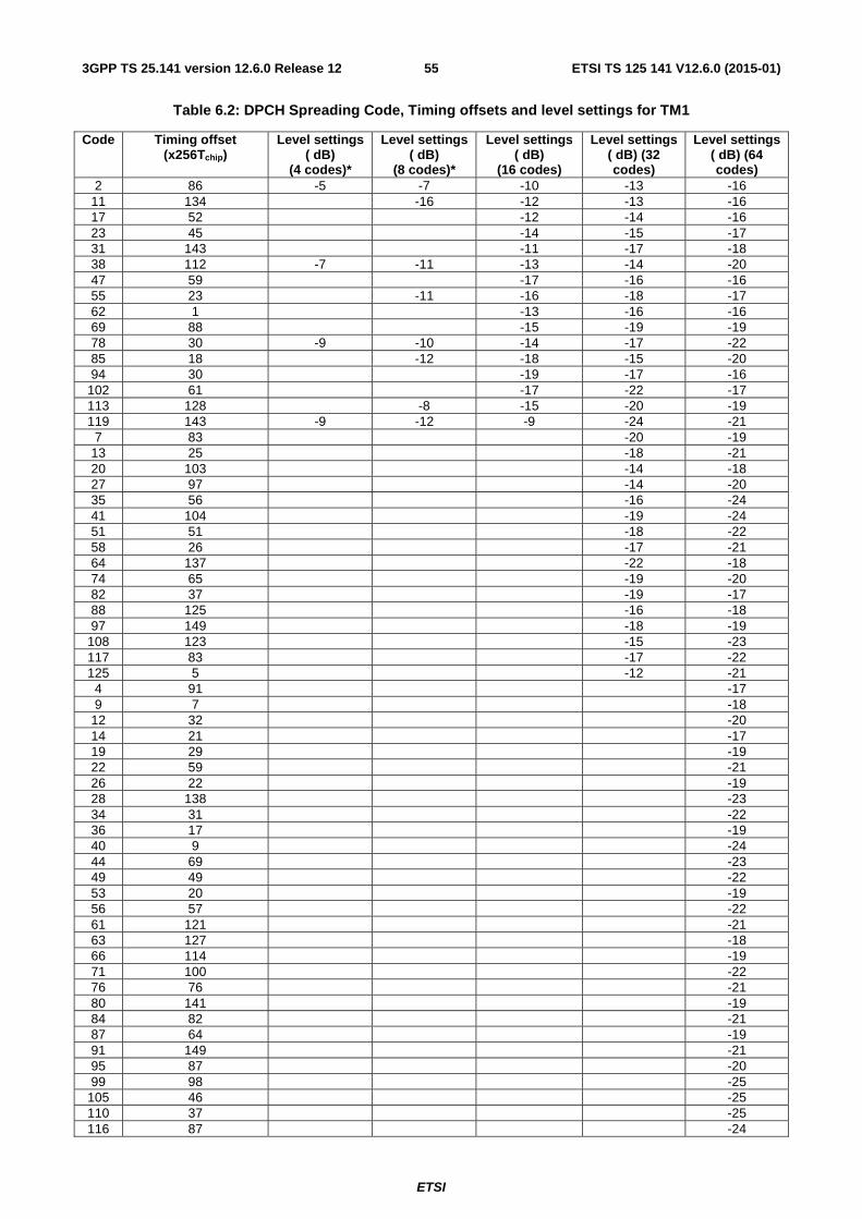
ETSI
ETSI TS 125 141 V12.6.0 (2015-01)553GPP TS 25.141 version 12.6.0 Release 12
Table 6.2: DPCH Spreading Code, Timing offsets and level settings for TM1
Code Timing offset (x256Tchip)
Level settings ( dB)
(4 codes)*
Level settings ( dB)
(8 codes)*
Level settings ( dB)
(16 codes)
Level settings ( dB) (32 codes)
Level settings ( dB) (64 codes)
2 86 -5 -7 -10 -13 -16 11 134 -16 -12 -13 -16 17 52 -12 -14 -16 23 45 -14 -15 -17 31 143 -11 -17 -18 38 112 -7 -11 -13 -14 -20 47 59 -17 -16 -16 55 23 -11 -16 -18 -17 62 1 -13 -16 -16 69 88 -15 -19 -19 78 30 -9 -10 -14 -17 -22 85 18 -12 -18 -15 -20 94 30 -19 -17 -16
102 61 -17 -22 -17 113 128 -8 -15 -20 -19 119 143 -9 -12 -9 -24 -21
7 83 -20 -19 13 25 -18 -21 20 103 -14 -18 27 97 -14 -20 35 56 -16 -24 41 104 -19 -24 51 51 -18 -22 58 26 -17 -21 64 137 -22 -18 74 65 -19 -20 82 37 -19 -17 88 125 -16 -18 97 149 -18 -19
108 123 -15 -23 117 83 -17 -22 125 5 -12 -21
4 91 -17 9 7 -18
12 32 -20 14 21 -17 19 29 -19 22 59 -21 26 22 -19 28 138 -23 34 31 -22 36 17 -19 40 9 -24 44 69 -23 49 49 -22 53 20 -19 56 57 -22 61 121 -21 63 127 -18 66 114 -19 71 100 -22 76 76 -21 80 141 -19 84 82 -21 87 64 -19 91 149 -21 95 87 -20 99 98 -25
105 46 -25 110 37 -25 116 87 -24

ETSI
ETSI TS 125 141 V12.6.0 (2015-01)563GPP TS 25.141 version 12.6.0 Release 12
Code Timing offset (x256Tchip)
Level settings ( dB)
(4 codes)*
Level settings ( dB)
(8 codes)*
Level settings ( dB)
(16 codes)
Level settings ( dB) (32 codes)
Level settings ( dB) (64 codes)
118 149 -22 122 85 -20 126 69 -15
Note *: Only applicable to Home BS
6.1.1.2 Test Model 2 – TM2
This model shall be used for tests on:
- output power dynamics.
- CPICH power accuracy.
Table 6.3: TM2 Active Channels
Type Number of Channels
Fraction of Power (%)
Level setting ( dB)
Channelization Code
Timing offset (x256Tchip)
P-CCPCH+SCH 1 10 -10 1 0 Primary CPICH 1 10 -10 0 0
PICH 1 5 -13 16 120 S-CCPCH containing
PCH (SF=256) 1 5 -13 3 0
DPCH (SF=128)
3 2 x 10,1 x 50 2 x -10, 1 x -3 24, 72, 120
1, 7, 2
6.1.1.3 Test Model 3 – TM3
This model shall be used for tests on:
- peak code domain error.
Table 6.4: TM3 Active Channels
Type Number of Channels
Fraction of Power (%) 4*/8*/16/32
Level settings ( dB)
4*/8*/16/32
Channelization Code
Timing offset (x256Tchip)
P-CCPCH+SCH 1 15,8/15,8/12,6/7,9
-8/ -8 / -9 / -11 1 0
Primary CPICH 1 15.8/15.8/12,6/7,9
-8 / -8 / -9 / -11 0 0
PICH 1 2.5/2.5/5/1.6 -16/-16/-13/-18 16 120 S-CCPCH containing
PCH (SF=256) 1 2.5/2.5/5/1.6 -16/-16/-13/-18 3 0
DPCH (SF=256)
4*/8*/16/32 63,4/63,4/63,7/80,4 in total
see table 6.5 see table 6.5 see table 6.5
Note *: Only applicable to Home BS
As with TM1, not every base station implementation will support 32 DPCH, a variant of this test model containing 16 DPCH are also specified. For Home base station, additional options of this test model containing 8 and 4 DPCH are also specified. The conformance test shall be performed using the larger of these options that can be supported by the equipment under test.

ETSI
ETSI TS 125 141 V12.6.0 (2015-01)573GPP TS 25.141 version 12.6.0 Release 12
Table 6.5: DPCH Spreading Code, Toffset and Power for TM3
Code Toffset Level settings ( dB) (4 codes)*
Level settings ( dB) (8 codes)*
Level settings ( dB) (16 codes)
Level settings ( dB) (32 codes)
64 86 -8 -11 -14 -16 69 134 -14 -16 74 52 -11 -14 -16 78 45 -14 -16 83 143 -14 -16 89 112 -8 -11 -14 -16 93 59 -14 -16 96 23 -11 -14 -16
100 1 -14 -16 105 88 -14 -16 109 30 -8 -11 -14 -16 111 18 -11 -14 -16 115 30 -14 -16 118 61 -14 -16 122 128 -11 -14 -16 125 143 -8 -11 -14 -16 67 83 -16 71 25 -16 76 103 -16 81 97 -16 86 56 -16 90 104 -16 95 51 -16 98 26 -16
103 137 -16 108 65 -16 110 37 -16 112 125 -16 117 149 -16 119 123 -16 123 83 -16 126 5 -16 Note *: Only applicable to Home BS
6.1.1.4 Test Model 4 – TM4
This model shall be used for tests on:
- EVM measurement
- Total power dynamic range
- Frequency error
Table 6.6: TM4 Active Channels
Type Number of Channels
Fraction of Power (%)
Level setting ( dB)
Channelization Code
Timing offset
PCCPCH+SCH when Primary
CPICH is disabled
1 1010100
X−
⋅
-X 1 0
PCCPCH+SCH when Primary
CPICH is enabled
1 10
3
10100−−
⋅X
-X-3 1 0
Primary CPICH1 1 10
3
10100−−
⋅X
-X-3 0 0
Note 1: The CPICH channel is optional.

ETSI
ETSI TS 125 141 V12.6.0 (2015-01)583GPP TS 25.141 version 12.6.0 Release 12
6.1.1.4A Test Model 5 – TM5
This model shall be used for tests on:
- EVM for base stations supporting HS-PDSCH transmission using 16QAM modulation (at Pmax)
Considering that not every base station implementation will support 8 HS-PDSCH + 30 DPCH, variants of this test model containing 4 HS-PDSCH + 14 DPCH and 2 HS-PDSCH + 6 DPCH are also specified. For Home base station, an additional option of this test model containing 4 HS-PDSCH + 4 DPCH is also specified. The conformance test shall be performed using the largest of these options that can be supported by the equipment under test, where the largest is firstly determined by the number of HS-PDSCH and then by the number of DPCH.
Each HS-PDSCH is modulated by 16QAM.
Table 6.6A: TM5 Active Channels
Type Number of Channels
Fraction of Power (%)
Level setting ( dB)
Channelization Code
Timing offset (x256Tchip)
P-CCPCH+SCH 1 7.9 -11 1 0 Primary CPICH 1 7.9 -11 0 0
PICH 1 1.3 -19 16 120 S-CCPCH containing
PCH (SF=256) 1 1.3 -19 3 0
DPCH (SF=128)
30/14/6/4(*) 14/14.2/14.4/14.2 in total
see table 6.6.B see table 6.6B see table 6.6.B
HS-SCCH 2 4 in total see table 6.6C see table 6.6C see table 6.6C
HS-PDSCH (16QAM) 8/4/2(*) 63.6/63.4/63.2 in total
see table 6.6D see table 6.6D see table 6.6D
Note *: 2 HS-PDSCH shall be taken together with 6 DPCH, 4 HS-PDSCH shall be taken with 14 DPCH or (for Home BS only) 4 DPCH, and 8 HS-PDSCH shall be taken together with 30 DPCH.

ETSI
ETSI TS 125 141 V12.6.0 (2015-01)593GPP TS 25.141 version 12.6.0 Release 12
Table 6.6B: DPCH Spreading Code, Timing offsets and level settings for TM5
Code (SF=128)
Timing offset (x256Tchip)
Level settings ( dB) (30 codes)
Level settings ( dB) (14 codes)
Level settings ( dB) (6 codes)
Level settings ( dB) (4 codes)*
15 86 -20 -17 -17 -15 23 134 -20 -19 -15 -15 68 52 -21 -19 -15 -18 76 45 -22 -20 -18 -12 82 143 -24 -18 -16 90 112 -21 -20 -17 5 59 -23 -25 11 23 -25 -23 17 1 -23 -20 27 88 -26 -22 64 30 -24 -21 72 18 -22 -22 86 30 -24 -19 94 61 -28 -20 3 128 -27 7 143 -26 13 83 -27 19 25 -25 21 103 -21 25 97 -21 31 56 -23 66 104 -26 70 51 -25 74 26 -24 78 137 -27 80 65 -26 84 37 -23 88 125 -25 89 149 -22 92 123 -24
Note *: Only applicable to Home BS
Table 6.6C: HS-SCCH Spreading Code, Timing offsets and level settings for TM5
Code (SF=128)
Timing offset (x256Tchip)
Level settings ( dB)
9 0 -15 29 0 -21
Table 6.6D: HS-PDSCH Spreading Code, Timing offsets, level settings for TM5
Code (SF=16)
Timing offset (x256Tchip)
Level settings ( dB)
(8 codes)
Level settings ( dB) (4 codes)
Level settings ( dB) (2 codes)
4 0 -11 -8 -5 5 0 -11 -8 6 0 -11 7 0 -11 12 0 -11 -8 -5 13 0 -11 -8 14 0 -11 15 0 -11
6.1.1.4B Test Model 6 – TM6
This model shall be used for tests on:
- Relative CDE for base stations supporting HS-PDSCH transmission using 64QAM modulation

ETSI
ETSI TS 125 141 V12.6.0 (2015-01)603GPP TS 25.141 version 12.6.0 Release 12
For Home base station, an additional option of this test model containing 4 HS-PDSCH + 4 DPCH is also specified. The conformance test shall be performed using the larger option that can be supported by the Home base station under test.
Each HS-PDSCH is modulated by 64QAM.
Table 6.6E: TM6 Active Channels
Type Number of Channels
Fraction of Power (%)
Level setting (dB)
Channelization Code
Timing offset (x256Tchip)
P-CCPCH+SCH 1 7.9 -11 1 0 Primary CPICH 1 7.9 -11 0 0
PICH 1 1.3 -19 16 120 S-CCPCH containing
PCH (SF=256) 1 1.3 -19 3 0
DPCH (SF=128)
30/4* 27.1 in total see table 6.6F see table 6.6F see table 6.6F
HS-SCCH 2 4 in total see table 6.6G see table 6.6G see table 6.6G HS-PDSCH (64QAM) 8/4* 50.5 in total see table 6.6H see table 6.6H see table 6.6H Note *: 8 HS-PDSCH shall be taken together with 30 DPCH, and (for Home BS only) 4 HS-PDSCH shall be
taken with 4 DPCH.
Table 6.6F: DPCH Spreading Code, Timing offsets and level settings for TM6
Code (SF=128)
Timing offset (x256Tchip)
Level settings (dB) (30 codes)
Level settings (dB) (4 codes)*
15 86 -17 -13 23 134 -17 -15 68 52 -18 -9 76 45 -19 -12 82 143 -21 90 112 -18 5 59 -20 11 23 -22 17 1 -20 27 88 -23 64 30 -21 72 18 -19 86 30 -21 94 61 -25 3 128 -24 7 143 -23 13 83 -24 19 25 -22 21 103 -18 25 97 -18 31 56 -20 66 104 -23 70 51 -22 74 26 -21 78 137 -24 80 65 -23 84 37 -22 88 125 -22 89 149 -22 92 123 -21
Note *: Only applicable to Home BS

ETSI
ETSI TS 125 141 V12.6.0 (2015-01)613GPP TS 25.141 version 12.6.0 Release 12
Table 6.6G: HS-SCCH Spreading Code, Timing offsets and level settings for TM6
Code (SF=128)
Timing offset (x256Tchip)
Level settings (dB)
9 0 -15 29 0 -21
Table 6.6H: HS-PDSCH Spreading Code, Timing offsets, level settings for TM6
Code (SF=16) Timing offset (x256Tchip) Level settings (dB) (8 codes)
Level settings (dB) (4 codes)*
4 0 -12 -9 5 0 -12 -9 6 0 -12 7 0 -12
12 0 -12 -9 13 0 -12 -9 14 0 -12 15 0 -12
Note *: Only applicable to Home BS
6.1.1.5 DPCH Structure of the Downlink Test Models
For the above test models the following structure is adopted for the DPCH. The DPDCH and DPCCH have the same power level. The timeslot structure should be as described by TS 25.211-slot format 10 and 6 that are reproduced in table 6.7.
Table 6.7: DPCH structure of the downlink Test Models
Slot Format
Channel Bit
Channel Symbol
SF Bits/Frame Bits/ Slot
DPDCH Bits/Slot DPCCH Bits/Slot
#I Rate (kbps)
Rate (ksps)
DPDCH DPCCH TOT NData1 Ndata2 NTFCI NTPC Npilot
10 60 30 128 450 150 600 40 6 24 0 2 8 6 30 15 256 150 150 300 20 2 8 0 2 8
The test DPCH has frame structure so that the pilot bits are defined over 15 timeslots according to the relevant columns of TS 25.211, which are reproduced in table 6.8.
Table 6.8: Frame structure of DPCH
Npilot = 8 Symbol # 0 1 2 3
Slot #0 1 2 3 4 5 6 7 8 9 10 11 12 13 14
11 11 11 11 11 11 11 11 11 11 11 11 11 11 11
11 00 01 00 10 11 11 10 01 11 01 10 10 00 00
11 11 11 11 11 11 11 11 11 11 11 11 11 11 11
10 10 01 00 01 10 00 00 10 11 01 11 00 11 11
The TPC bits alternate 00 / 11 starting with 00 in timeslot 0.

ETSI
ETSI TS 125 141 V12.6.0 (2015-01)623GPP TS 25.141 version 12.6.0 Release 12
The aggregate 15 x 30 = 450 DPDCH bits per frame are filled with a PN9 sequence generated using the primitive
trinomial 9 4 1x x+ + . In case there are less data bits/frame needed then the first bits of the aggregate shall be selected. To ensure non-correlation of the PN9 sequences, each DPDCH shall use its channelization code as the seed for the PN sequence at the start of each frame, according to its timing offset.
The sequence shall be generated in a nine-stage shift register whose 5th and 9th stage outputs are added in a modulo-two addition stage, and the result is fed back to the input of the first stage. The generator shall be seeded so that the sequence begins with the channelization code starting from the LSB, and followed by 2 consecutive ONEs for SF=128 and 1 consecutive ONE for SF=256.
LSB MSB 1 0 2 3 4 5 6 7 8
Figure 6.2
6.1.1.6 Common channel Structure of the Downlink Test Models
6.1.1.6.1 P-CCPCH
The aggregate 15 x 18 = 270 P-CCPCH bits per frame are filled with a PN9 sequence generated using the primitive
trinomial 9 4 1x x+ + . Channelization code of the P-CCPCH is used as the seed for the PN sequence at the start of each frame.
The generator shall be seeded so that the sequence begins with the 8 bit channelization code starting from the LSB, and followed by a ONE.
6.1.1.6.2 PICH
PICH carries 18 Paging Indicators (Pq) sent in the following sequence from left to right [1 0 1 1 0 0 0 1 0 1 1 0 0 0 1 0 1 0]. This defines the 288 first bits of the PICH. No power is transmitted for the 12 remaining unused bits.
6.1.1.6.3 Primary scrambling code and SCH
The scrambling code should be 0.
Where multiple repetitions of the Test Model signals are being used to simulate a multi-carrier signal the scrambling code for the lower frequency is 0. Carriers added at successively higher frequencies use codes 1, 2,... and their frame structures are time offset by 1/5, 2/5... of a time slot duration.
The scrambling code defines the SSC sequence of the secondary SCH. In their active part, primary and secondary SCH share equally the power level defined for "PCCPCH+SCH".
6.1.1.6.4 S-CCPCH containing PCH
The aggregate 15 x 20 = 300 S-CCPCH bits per frame are used. Data bits are filled with a PN9 sequence generated
using the primitive trinomial 9 4 1x x+ + . In case there are less data bits/frame needed then the first bits of the aggregate shall be selected.. Channelization code of the S-CCPCH is used as the seed for the PN sequence at the start of each frame. For test purposes, any one of the four possible slot formats 0,1, 2 and 3 can be supported. The support for all four slot formats is not needed..
The generator shall be seeded so that the sequence begins with the 8 bit channelization code starting from the LSB, and followed by a ONE. The test on S-CCPCH has a frame structure so that the pilot bits are defined over 15 timeslots to the relevant columns of TS 25.211. The TFCI bits are filled with ONEs whenever needed.
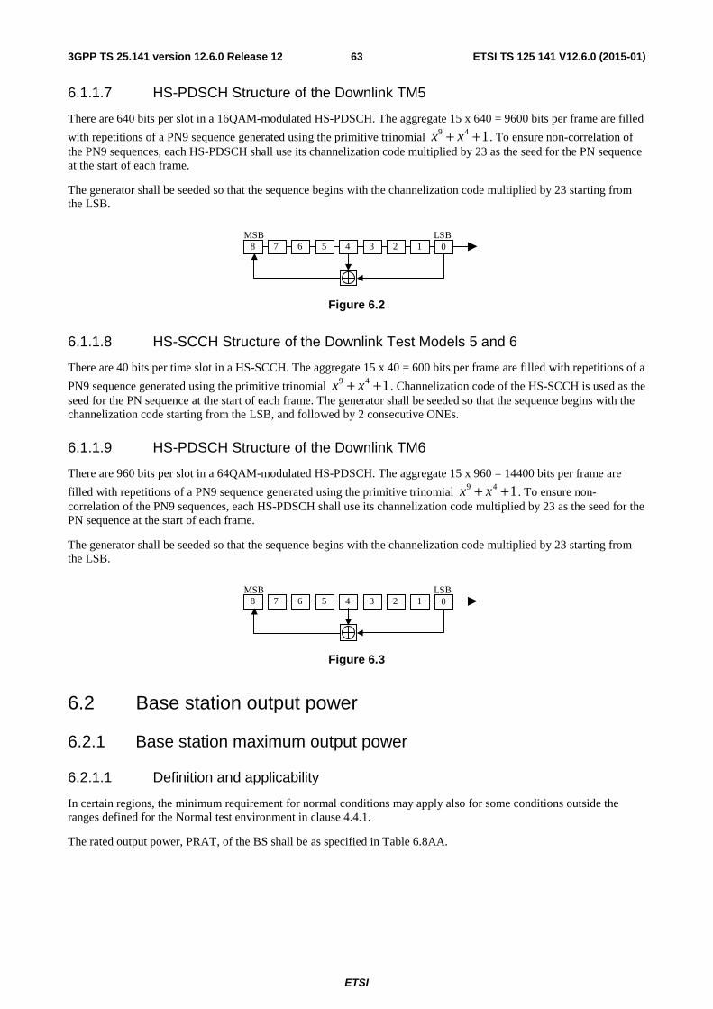
ETSI
ETSI TS 125 141 V12.6.0 (2015-01)633GPP TS 25.141 version 12.6.0 Release 12
6.1.1.7 HS-PDSCH Structure of the Downlink TM5
There are 640 bits per slot in a 16QAM-modulated HS-PDSCH. The aggregate 15 x 640 = 9600 bits per frame are filled
with repetitions of a PN9 sequence generated using the primitive trinomial 9 4 1x x+ + . To ensure non-correlation of the PN9 sequences, each HS-PDSCH shall use its channelization code multiplied by 23 as the seed for the PN sequence at the start of each frame.
The generator shall be seeded so that the sequence begins with the channelization code multiplied by 23 starting from the LSB.
LSB MSB 1 0 2 3 4 5 6 7 8
Figure 6.2
6.1.1.8 HS-SCCH Structure of the Downlink Test Models 5 and 6
There are 40 bits per time slot in a HS-SCCH. The aggregate 15 x 40 = 600 bits per frame are filled with repetitions of a
PN9 sequence generated using the primitive trinomial 9 4 1x x+ + . Channelization code of the HS-SCCH is used as the seed for the PN sequence at the start of each frame. The generator shall be seeded so that the sequence begins with the channelization code starting from the LSB, and followed by 2 consecutive ONEs.
6.1.1.9 HS-PDSCH Structure of the Downlink TM6
There are 960 bits per slot in a 64QAM-modulated HS-PDSCH. The aggregate 15 x 960 = 14400 bits per frame are
filled with repetitions of a PN9 sequence generated using the primitive trinomial 9 4 1x x+ + . To ensure non-correlation of the PN9 sequences, each HS-PDSCH shall use its channelization code multiplied by 23 as the seed for the PN sequence at the start of each frame.
The generator shall be seeded so that the sequence begins with the channelization code multiplied by 23 starting from the LSB.
LSB MSB 1 0 2 3 4 5 6 7 8
Figure 6.3
6.2 Base station output power
6.2.1 Base station maximum output power
6.2.1.1 Definition and applicability
In certain regions, the minimum requirement for normal conditions may apply also for some conditions outside the ranges defined for the Normal test environment in clause 4.4.1.
The rated output power, PRAT, of the BS shall be as specified in Table 6.8AA.

ETSI
ETSI TS 125 141 V12.6.0 (2015-01)643GPP TS 25.141 version 12.6.0 Release 12
Table 6.8AA: Base Station rated output power
BS class PRAT Wide Area BS - (note)
Medium Range BS < +38 dBm Local Area BS < + 24 dBm
Home BS < + 20 dBm (without transmit diversity or MIMO)
< + 17 dBm (with transmit diversity or MIMO mode with two transmlt
antennas) < + 14 dBm (with MIMO mode with
four transmit antennas) NOTE: There is no upper limit required for the rated output power of the
Wide Area Base Station like for the base station for General Purpose application in Release 99, 4, and 5.
6.2.1.2 Minimum Requirement
The minimum requirement is in TS 25.104 [1] clause 6.2.1.
6.2.1.3 Test purpose
The test purpose is to verify the accuracy of the maximum output power across the frequency range and under normal and extreme conditions for all transmitters in the BS.
6.2.1.4 Method of test
6.2.1.4.1 Initial conditions
Test environment: normal; see clause 4.4.1.
RF channels to be tested for single carrier: B, M and T; see clause 4.8.
RF bandwidth positions to be tested for multi-carrier: BRFBW, MRFBW and TRFBW in single band operation; BRFBW_T"RFBW and B"RFBW_TRFBW in multi-band operation; see subclause 4.8.1.
In addition, for only one UARFCN or BS RF bandwidth position, the test shall be performed under extreme power supply as defined in clause 4.4.4
NOTE: Tests under extreme power supply also test extreme temperature.
1) Connect the power measuring equipment to the base station antenna connector.
6.2.1.4.2 Procedure
1) For a BS declared to be capable of single carrier operation only, set the BS to transmit a signal in accordance to TM1, clause 6.1.1.1, at manufacturer"s declared rated output power, PRAT.
For a BS declared to be capable of multi-carrier operation, set the base station to transmit according to TM1 on all carriers configured using the applicable test configuration and corresponding power setting specified in sub-clause 4.12.
2) Measure the mean power for each carrier, Pout, at the BS antenna connector.
In addition, for a multi-band capable BS, the following steps shall apply:
3) For multi-band capable BS and single band tests, repeat the steps above per involved band where single band test configurations and test models shall apply with no carrier activated in the other band.
4) For multi-band capable BS with separate antenna connector, the antenna connector not being under test in case of single-band or multi-band test shall be terminated.

ETSI
ETSI TS 125 141 V12.6.0 (2015-01)653GPP TS 25.141 version 12.6.0 Release 12
6.2.1.5 Test Requirements
In normal conditions, the measurement result in step 2 of 6.2.1.4.2 shall remain:
within +2.7 dB and -2.7 dB of the manufacturer's rated output power, PRAT, for carrier frequency f ≤ 3.0 GHz,
within +3.0 dB and –3.0 dB of the manufacturer's rated output power, PRAT, for carrier frequency 3.0 GHz < f ≤ 4.2 GHz.
In extreme conditions, measurement result in step 2 of 6.2.1.4.2 shall remain:
within +3.2 dB and -3.2 dB of the manufacturer's rated output power, PRAT, for carrier frequency f ≤ 3.0 GHz,
within +3.5 dB and –3.5 dB of the manufacturer's rated output power, PRAT, for carrier frequency 3.0 GHz < f ≤ 4.2 GHz.
NOTE: If the above Test Requirement differs from the Minimum Requirement then the Test Tolerance applied for this test is non-zero. The Test Tolerance for this test is defined in clause 4.2 and the explanation of how the Minimum Requirement has been relaxed by the Test Tolerance is given in Annex F.
6.2.2 Primary CPICH power accuracy
6.2.2.1 Definition and applicability
Primary CPICH (P-CPICH) power is the code domain power of the Primary Common Pilot Channel. P-CPICH power is indicated on the BCH. The requirement is applicable for all BS types.
6.2.2.2 Minimum Requirement
The minimum requirement is in TS 25.104 [1] clause 6.4.4.
6.2.2.3 Test purpose
The purpose of the test is to verify, that the BS under test delivers Primary CPICH code domain power within margins, thereby allowing reliable cell planning and operation.
6.2.2.4 Method of test
6.2.2.4.1 Initial conditions
Test environment: normal; see clause 4.4.1.
RF channels to be tested: B, M and T; see clause 4.8
1) Connect BS to code domain analyser as shown in annex B.1.2.
2) Disable inner loop power control.
3) Set the BS to transmit a signal in accordance to TM2, clause 6.1.1.2, at manufacturer"s declared rated output power, PRAT. In case of transmit diversity or MIMO transmission the configured Primary CPICH code domain power per antenna connector shall be declared by the manufactuer.
6.2.2.4.2 Procedure
- Measure the P-CPICH power in one timeslot according to annex E.
In addition, for a multi-band capable BS, the following steps shall apply:
1) For multi-band capable BS and single band tests, repeat the steps above per involved band where single carrier test models shall apply with no carrier activated in the other band.

ETSI
ETSI TS 125 141 V12.6.0 (2015-01)663GPP TS 25.141 version 12.6.0 Release 12
2) For multi-band capable BS with separate antenna connector, the antenna connector not being under test shall be terminated.
6.2.2.5 Test Requirement
The measured P-CPICH code domain power shall be:
within ±2.9 dB of the configured absolute value for carrier frequency f ≤ 3.0 GHz
within +3.2 dB and –3.2 dB of the configured absolute value for carrier frequency 3.0 GHz < f ≤ 4.2 GHz.
NOTE: If the above Test Requirement differs from the Minimum Requirement then the Test Tolerance applied for this test is non-zero. The Test Tolerance for this test is defined in clause 4.2 and the explanation of how the Minimum Requirement has been relaxed by the Test Tolerance is given in Annex F.
6.2.3 Secondary CPICH power offset accuracy
6.2.3.1 Definition and applicability
Secondary CPICH (S-CPICH) power is the code domain power of the Secondary Common Pilot Channel. S-CPICH power is equal to the sum of the P-CPICH power and the power offset, which are signalled to the UE. The power offset for MIMO mode is signalled in the IE 'Power Offset for S-CPICH for MIMO', defined in section 10.3.6.41b in TS 25.331. The requirement is applicable for BS supporting MIMO operation. If the manufacturer declares the implementation of a Virtual Antenna Mapping (VAM), then this test will not be performed.
For MIMO mode with four transmit antennas, the power offset of S-CPICH on antenna 2 is signalled in the IE 'Power Offset for S-CPICH for MIMO mode with four transmit antennas on Antenna2' as defined in section 10.3.6.143 in TS 25.331 [11]. The power offset of S-CPICH on antenna 3 and 4 is signalled in the IE 'Common Power Offset for S-CPICH for MIMO mode with four transmit antennas on Antenna 3 and 4', as defined in section 10.3.6.143 in TS 25.331.
6.2.3.2 Minimum Requirement
The minimum requirement is in TS 25.104 [1] clause 6.4.4A.1 for MIMO mode and in subclause 6.4.4A.2 for MIMO mode with four transmit antennas.
6.2.3.3 Test purpose
The purpose of the test is to verify, that the BS under test delivers the advertised power offset for S-CPICH power within margins, thereby allowing reliable MIMO HS-DSCH demodulation and CQI reporting.
6.2.3.4 Method of test for MIMO mode
6.2.3.4.1 Initial conditions
Test environment: normal; see clause 4.4.1.
RF channels to be tested: B, M and T; see clause 4.8
1) Connect BS to code domain analyser as shown in annex B.1.2. Figure B.2A.
2) Disable inner loop power control.
3) Set the BS to transmit a signal in accordance to TM2, clause 6.1.1.2, at manufacturer"s declared rated output power, PRAT. The configured Primary CPICH code domain power intended per antenna connector shall be declared by the manufactuer.
4) The same BS set up is applied on both the antenna connectors.

ETSI
ETSI TS 125 141 V12.6.0 (2015-01)673GPP TS 25.141 version 12.6.0 Release 12
6.2.3.4.2 Procedure
- During the same timeslot:
1) Measure the P-CPICH power, according to annex E on first antenna connector.
2) Measure the P-CPICH power, according to annex E on second antenna connector.
In addition, for a multi-band capable BS, the following steps shall apply:
3) For multi-band capable BS and single band tests, repeat the steps above per involved band where single carrier test models shall apply with no carrier activated in the other band.
4) For multi-band capable BS with separate antenna connector, the antenna connector not being under test shall be terminated.
6.2.3.4A Method of test for MIMO mode with four transmit antennas
6.2.3.4A.1 Initial conditions
Test environment: normal; see subclause 4.4.1.
RF channels to be tested: B, M and T; see subclause 4.8
1) Connect BS to code domain analyser analyser as shown in annex B.1.2. Figure B.2A.
2) Disable inner loop power control.
3) Set-up BS transmission at manufacturer"s declared rated output power per carrier, PRAT. Channel set-up shall be according to TM2 subclause 6.1.1.2. Primary CPICH code domain power intended per antenna connector shall be declared by the manufactuer.
4) The same BS set up is applied on antenna connectors 1, 2, 3, 4.
6.2.3.4A.2 Procedure
a) Measure the P-CPICH power, on first antenna connector.
b) Measure the P-CPICH power, on second antenna connector.
c) Measure the P-CPICH power, on third antenna connector.
d) Measure the P-CPICH power, on fourth antenna connector.
6.2.3.5 Test Requirement for MIMO mode
The difference between measured P-CPICH power on two different antenna connectors shall be:
within ±2.7 dB for carrier frequency f ≤ 3.0 GHz,
within ±3.0 dB for carrier frequency 3.0 GHz < f ≤ 4.2 GHz.
NOTE: If the above Test Requirement differs from the Minimum Requirement then the Test Tolerance applied for this test is non-zero. The Test Tolerance for this test is defined in clause 4.2 and the explanation of how the Minimum Requirement has been relaxed by the Test Tolerance is given in Annex F.
6.2.3.5A Test Requirement for MIMO mode with four transmit antennas
The difference between measured P-CPICH powers on any two different antenna connectors shall be:
within ±2.7 dB for carrier frequency f ≤ 3.0 GHz,
within ±3.0 dB for carrier frequency 3.0 GHz < f ≤ 4.2 GHz.

ETSI
ETSI TS 125 141 V12.6.0 (2015-01)683GPP TS 25.141 version 12.6.0 Release 12
NOTE: If the above Test Requirement differs from the Minimum Requirement then the Test Tolerance applied for this test is non-zero. The Test Tolerance for this test is defined in subclause 4.2 and the explanation of how the Minimum Requirement has been relaxed by the Test Tolerance is given in Annex F.
6.3 Frequency error
6.3.1 Definition and applicability
Frequency error is the measure of the difference between the actual BS transmit frequency and the assigned frequency. The same source shall be used for RF frequency and data clock generation.
It is not possible to verify by testing that the data clock is derived from the same frequency source as used for RF generation. This may be confirmed by a manufacturers declaration
6.3.2 Minimum Requirement
The minimum requirement is in TS 25.104 [1] clause 6.3.
Table 6.8A: (void)
6.3.3 Test purpose
To verify that the Frequency Error is within the limit of the minimum requirement.
6.3.4 Method of test
Requirement is tested together with Error Vector Magnitude test, as described in clause 6.7.1.4.
6.3.5 Test requirement
The Frequency Error for every measured slot shall be between the minimum and maximum value specified in Table 6.8B.
Table 6.8B: Frequency error test requirement
BS class Minimum frequency error
Maximum frequency error
Wide Area BS -0.05 ppm - 12 Hz +0.05 ppm + 12 Hz Medium Range BS -0.1 ppm - 12 Hz +0.1 ppm + 12 Hz
Local Area BS -0.1 ppm - 12 Hz +0.1 ppm + 12 Hz Home BS -0.25 ppm - 12 Hz +0.25 ppm + 12 Hz
NOTE: If the above Test Requirement differs from the Minimum Requirement then the Test Tolerance applied for this test is non-zero. The Test Tolerance for this test is defined in clause 4.2 and the explanation of how the Minimum Requirement has been relaxed by the Test Tolerance is given in Annex F.
6.4 Output power dynamics Power control is used to limit the interference level. The BS transmitter uses a quality-based power control on the downlink. The physical channels for the following test(s) shall be set-up according to clause 6.1.1.2.
6.4.1 Inner loop power control
Inner loop power control in the downlink is the ability of the BS transmitter to adjust the code domain power of a code channel in accordance with the corresponding TPC symbols received in the uplink.
ETSI
ETSI TS 125 141 V12.6.0 (2015-01)693GPP TS 25.141 version 12.6.0 Release 12
6.4.2 Power control steps
The power control step is the required step change in the code domain power of a code channel in response to the corresponding power control command. The combined output power change is the required total change in the DL transmitter output power of a code channel in response to multiple consecutive power control commands corresponding to that code channel.
6.4.2.1 Definition and applicability
Inner loop power control in the downlink is the ability of the BS transmitter to adjust the transmitter output power of a code channel in accordance with the corresponding TPC symbols received in the uplink.
The power control step is the required step change in the DL transmitter output power of a code channel in response to the corresponding power control command. The combined output power change is the required total change in the DL transmitter output power of a code channel in response to multiple consecutive power control commands corresponding to that code channel.
6.4.2.2 Minimum Requirement
The minimum requirement is in TS 25.104 [1] clause 6.4.1.1.1.
Table 6.9: (void)
Table 6.10: (void)
6.4.2.3 Test purpose
To verify those requirements for the power control step size and response are met as specified in clause 6.4.2.2.
6.4.2.4 Method of test
6.4.2.4.1 Initial conditions
Test environment: normal; see clause 4.4.1.
RF channels to be tested: B, M and T; see clause 4.8
1) Connect the suitable measurement equipment to the BS antenna connector as shown in annex B.
2) Set the BS to transmit a signal in accordance to TM2, clause 6.1.1.2, at manufacturer"s declared rated output power, PRAT.
The DPCH intended for power control is on channel 120 starting at -3 dB.
3) Establish downlink power control with parameters as specified in table 6.11.
Table 6.11
Parameter Level/status Unit UL signal mean power Ref.sens + 10 dB dBm Data sequence PN9
6.4.2.4.2 Procedure
1) Set and send alternating TPC bits from the UE simulator or UL signal generator.
2) Measure mean power level of the code under the test each time TPC command is transmitted. All steps within power control dynamic range declared by manufacturer shall be measured. Use the code domain power measurement method defined in annex E.

ETSI
ETSI TS 125 141 V12.6.0 (2015-01)703GPP TS 25.141 version 12.6.0 Release 12
3) Measure the 10 highest and the 10 lowest power step levels within the power control dynamic range declared by manufacturer by sending 10 consecutive equal commands as described table 6.10.
In addition, for a multi-band capable BS, the following steps shall apply:
4) For multi-band capable BS and single band tests, repeat the steps above per involved band where single carrier test models shall apply with no carrier activated in the other band.
5) For multi-band capable BS with separate antenna connector, the antenna connector not being under test shall be terminated.
6.4.2.5 Test requirement
a) BS shall fulfil step size requirement shown in Table 6.12 for all power control steps declared by manufacture as specified in clause 6.4.2.2.
b) For all measured Up/Down cycles, the difference of code domain power between before and after 10 equal commands (Up and Down), derived in step (3), shall not exceed the prescribed tolerance in table 6.13.
Table 6.12: Transmitter power control step tolerance
Power control commands in the downlink
Transmitter power control step tolerance
2 dB step size 1.5 dB step size 1 dB step size 0.5 dB step size Lower Upper Lower Upper Lower Upper Lower Upper
Up(TPC command "1") +0.9 dB +3.1 dB +0.65 dB +2.35 dB +0.4 dB +1.6 dB +0.15 dB +0.85 dB Down(TPC command "0") -0.9 dB -3.1 dB -0.65 dB -2.35 dB -0.4 dB -1.6 dB -0.15 dB -0.85 dB
Table 6.13: Transmitter aggregated power control step range
Power control commands in the downlink
Transmitter aggregated power control step range after 10 consecutive equal commands (up or down)
2 dB step size 1.5 dB step size 1 dB step size 0.5 dB step size Lower Upper Lower Upper Lower Upper Lower Upper
Up(TPC command "1") +15.9 dB +24.1 dB +11.9 dB +18.1 dB +7.9 dB +12.1 dB +3.9 dB +6.1 dB Down(TPC command "0") -15.9 dB -24.1 dB -11.9 dB -18.1 dB -7.9 dB -12.1 dB -3.9 dB -6.1 dB
NOTE: If the above Test Requirement differs from the Minimum Requirement then the Test Tolerance applied for this test is non-zero. The Test Tolerance for this test is defined in clause 4.2 and the explanation of how the Minimum Requirement has been relaxed by the Test Tolerance is given in Annex F.
6.4.3 Power control dynamic range
6.4.3.1 Definition and applicability
The power control dynamic range is the difference between the maximum and the minimum code domain power of a code channel for a specified reference condition. Transmit modulation quality shall be maintained within the whole dynamic range as specified in TS 25.104 [1] clause 6.8.
6.4.3.2 Minimum Requirement
The minimum requirement is in TS 25.104 [1] clause 6.4.2.1.
6.4.3.3 Test purpose
To verify that the minimum power control dynamic range is met as specified by the minimum requirement.

ETSI
ETSI TS 125 141 V12.6.0 (2015-01)713GPP TS 25.141 version 12.6.0 Release 12
6.4.3.4 Method of test
6.4.3.4.1 Initial conditions
Test environment: normal; see clause 4.4.1.
RF channels to be tested: B, M and T; see clause 4.8Connect the measurement equipment to the BS antenna connector as shown in annex B.
6.4.3.4.2 Procedure
1) Set the BS to transmit a signal in accordance to TM2, clause 6.1.1.2, at manufacturers declared rated output power, PRAT.
2) Using TM2,set the code domain power of the DPCH under test to PRAT - 3 dB. Power levels for other code channels may be adjusted if necessary.
3) Measure the code domain power of the code channel under test. Use the code domain power measurement method defined in annex E.
4) Set the code domain power of the DPCH under test to PRAT - 28 dB by means determined by the manufacturer. The power levels for the other code channels used in step 2 shall remain unchanged (the overall output power will drop by approximately 3 dB).
5) Measure the code domain power of the code channel under test.
In addition, for a multi-band capable BS, the following steps shall apply:
6) For multi-band capable BS and single band tests, repeat the steps above per involved band where single carrier test models shall apply with no carrier activated in the other band.
7) For multi-band capable BS with separate antenna connector, the antenna connector not being under test shall be terminated.
6.4.3.5 Test requirement
Downlink (DL) power control dynamic range:
- maximum code domain power: BS maximum output power -4.1 dB or greater;
- minimum code domain power: BS maximum output power -26.9 dB or less.
NOTE: If the above Test Requirement differs from the Minimum Requirement then the Test Tolerance applied for this test is non-zero. The Test Tolerance for this test is defined in clause 4.2 and the explanation of how the Minimum Requirement has been relaxed by the Test Tolerance is given in Annex F.
6.4.4 Total power dynamic range
6.4.4.1 Definition and applicability
The downlink total power dynamic range is the difference between the maximum and the minimum output power per carrier for a specified reference condition.
6.4.4.2 Minimum Requirement
The minimum requirement is in TS 25.104 [1] clause 6.4.3.1.
6.4.4.3 Test purpose
To verify that the total power dynamic range is met as specified by the minimum requirement. The test is to ensure that the total output power can be reduced while still transmitting a single code. This is to ensure that the interference to neighbouring cells is reduced.

ETSI
ETSI TS 125 141 V12.6.0 (2015-01)723GPP TS 25.141 version 12.6.0 Release 12
6.4.4.4 Method of test
6.4.4.4.1 Initial Conditions
Test environment: normal; see clause 4.4.1.
RF channels to be tested: B, M and T; see clause 4.8
RF bandwidth positions to be tested for multi-carrier: BRFBW, MRFBW and TRFBW in single band operation; see subclause 4.8.1.
Refer to annex B for a functional block diagram of the test set-up.
1) Connect the base station antenna connector to the measurement equipment.
6.4.4.4.2 Procedure
The downlink total dynamic range is computed as the difference of the maximum carrier output power, measured as defined in step 2 in clause 6.2.1.4.2 and the carrier power measured at step 3 of the Error Vector Magnitude test, as described in clause 6.7.1.4.2.
In addition, for a multi-band capable BS, the following steps shall apply:
1) For multi-band capable BS and single band tests, repeat the steps above per involved band where single carrier test models shall apply with no carrier activated in the other band.
2) For multi-band capable BS with separate antenna connector, the antenna connector not being under test shall be terminated.
6.4.4.5 Test requirement
The downlink total power dynamic range shall be 17.7 dB or greater.
NOTE: If the above Test Requirement differs from the Minimum Requirement then the Test Tolerance applied for this test is non-zero. The Test Tolerance for this test is defined in clause 4.2 and the explanation of how the Minimum Requirement has been relaxed by the Test Tolerance is given in Annex F.
6.4.5 IPDL time mask
6.4.5.1 Definition and applicability
To support IPDL location method, the Node B shall interrupt all transmitted signals in the downlink (i.e. common and dedicated channels).
The IPDL time mask specifies the limits of the BS output power during these idle periods.
The requirement in this section shall apply to BS supporting IPDL. The requirement applies to all output powers within the total power dynamic range as specified in TS 25.104 [1] clause 6.4.3.
6.4.5.2 Minimum Requirement
The minimum requirement is in TS 25.104 [1] clause 6.4.5.1.
6.4.5.3 Test purpose
The test purpose is to verify the ability of the BS to temporarily reduce its output power below a specified value to improve time difference measurements made by UE for location services.

ETSI
ETSI TS 125 141 V12.6.0 (2015-01)733GPP TS 25.141 version 12.6.0 Release 12
6.4.5.4 Method of test
6.4.5.4.1 Initial conditions
Test environment: normal; see clause 4.4.1.
RF channels to be tested: B, M and T; see clause 4.8.
1) Connect the power measuring equipment to the BS antenna connector.
2) Set the BS to transmit a signal in accordance to TM1, clause 6.1.1.1, at manufacturer"s declared rated output power, PRAT.
3) Configure the BS to produce idle periods in continuous mode. The IPDL parameters as defined in TS 25.214 [12] shall have the following values:
IP_Spacing = 5
IP_Length = 10 CPICH symbols
Seed = 0
6.4.5.4.2 Procedure
1) Measure the mean power at the BS antenna connector over a period starting 27 chips after the beginning of the IPDL period and ending 27 chips before the expiration of the IPDL period.
In addition, for a multi-band capable BS, the following steps shall apply:
2) For multi-band capable BS and single band tests, repeat the step above per involved band where single carrier test models shall apply with no carrier activated in the other band.
3) For multi-band capable BS with separate antenna connector, the antenna connector not being under test shall be terminated.
6.4.5.5 Test Requirements
The mean power measured according to step (1) in clause 6.4.5.4.2 shall be equal to or less than
BS maximum output power - 34.3 dB.
See also Figure 6.4
27 chips 27 chips
BS maximum output power
34.3 dB
IP_Length
Figure 6.4: IPDL Time Mask
NOTE: If the above Test Requirement differs from the Minimum Requirement then the Test Tolerance applied for this test is non-zero. The Test Tolerance for this test is defined in clause 4.2 and the explanation of how the Minimum Requirement has been relaxed by the Test Tolerance is given in Annex F.
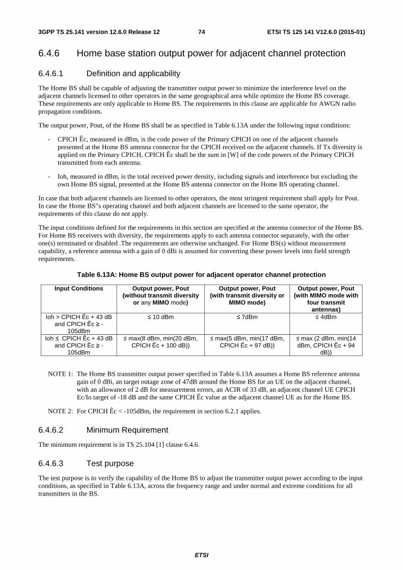
ETSI
ETSI TS 125 141 V12.6.0 (2015-01)743GPP TS 25.141 version 12.6.0 Release 12
6.4.6 Home base station output power for adjacent channel protection
6.4.6.1 Definition and applicability
The Home BS shall be capable of adjusting the transmitter output power to minimize the interference level on the adjacent channels licensed to other operators in the same geographical area while optimize the Home BS coverage. These requirements are only applicable to Home BS. The requirements in this clause are applicable for AWGN radio propagation conditions.
The output power, Pout, of the Home BS shall be as specified in Table 6.13A under the following input conditions:
- CPICH Êc, measured in dBm, is the code power of the Primary CPICH on one of the adjacent channels presented at the Home BS antenna connector for the CPICH received on the adjacent channels. If Tx diversity is applied on the Primary CPICH, CPICH Êc shall be the sum in [W] of the code powers of the Primary CPICH transmitted from each antenna.
- Ioh, measured in dBm, is the total received power density, including signals and interference but excluding the own Home BS signal, presented at the Home BS antenna connector on the Home BS operating channel.
In case that both adjacent channels are licensed to other operators, the most stringent requirement shall apply for Pout. In case the Home BS"s operating channel and both adjacent channels are licensed to the same operator, the requirements of this clause do not apply.
The input conditions defined for the requirements in this section are specified at the antenna connector of the Home BS. For Home BS receivers with diversity, the requirements apply to each antenna connector separately, with the other one(s) terminated or disabled .The requirements are otherwise unchanged. For Home BS(s) without measurement capability, a reference antenna with a gain of 0 dBi is assumed for converting these power levels into field strength requirements.
Table 6.13A: Home BS output power for adjacent operator channel protection
Input Conditions Output power, Pout (without transmit diversity
or any MIMO mode)
Output power, Pout (with transmit diversity or
MIMO mode)
Output power, Pout (with MIMO mode with
four transmit antennas)
Ioh > CPICH Êc + 43 dB and CPICH Êc ≥ -
105dBm
≤ 10 dBm ≤ 7dBm ≤ 4dBm
Ioh ≤ CPICH Êc + 43 dB and CPICH Êc ≥ -
105dBm
≤ max(8 dBm, min(20 dBm, CPICH Êc + 100 dB))
≤ max(5 dBm, min(17 dBm, CPICH Êc + 97 dB))
≤ max (2 dBm, min(14 dBm, CPICH Êc + 94
dB))
NOTE 1: The Home BS transmitter output power specified in Table 6.13A assumes a Home BS reference antenna gain of 0 dBi, an target outage zone of 47dB around the Home BS for an UE on the adjacent channel, with an allowance of 2 dB for measurement errors, an ACIR of 33 dB, an adjacent channel UE CPICH Ec/Io target of -18 dB and the same CPICH Êc value at the adjacent channel UE as for the Home BS.
NOTE 2: For CPICH Êc < -105dBm, the requirement in section 6.2.1 applies.
6.4.6.2 Minimum Requirement
The minimum requirement is in TS 25.104 [1] clause 6.4.6.
6.4.6.3 Test purpose
The test purpose is to verify the capability of the Home BS to adjust the transmitter output power according to the input conditions, as specified in Table 6.13A, across the frequency range and under normal and extreme conditions for all transmitters in the BS.

ETSI
ETSI TS 125 141 V12.6.0 (2015-01)753GPP TS 25.141 version 12.6.0 Release 12
6.4.6.4 Method of test
6.4.6.4.1 Initial conditions
Test environment: normal; see clause 4.4.1.
RF channels to be tested: M; see clause 4.8
In addition, on one UARFCN only, the test shall be performed under extreme power supply as defined in clause 4.4.4
NOTE: Tests under extreme power supply also test extreme temperature.
Signal generators delivering co-channel and adjacent channel interferers are switched off.
1) Set-up the equipment as shown as shown in Annex B.1.7.
2) The Home BS is configured such that the adjacent channel is known to belong to another operator.
6.4.6.4.2 Procedure
1) Connect the combined downlink interfering signals (referred to as point D in Figure B.7) to the dedicated measurement port (referred to as point 1 in Figure B.7) if available, otherwise connect to point 2.
2) Configure the signal generator for co-channel interference to transmit AWGN over a 3.84MHz bandwidth centred on RF channel M.
3) Configure the signal generator for adjacent channel DL signal to transmit TM1 at the centre frequency equal to RF channel M +5 MHz.
4) Switch on signal generators delivering co-channel and adjacent channel interferers, and adjust the ATT1 and ATT2 such that CPICH Êc = -80 dBm and Ioh = -50 dBm.
5) Trigger the Home BS power adjustment mechanism.
6) Set the Home BS to transmit a signal in accordance to TM1, clause 6.1.1.1
NOTE: The signal shall be transmitted with the maximum allowed output power.
7) Measure Home BS output power, Pout, and check it is below the required value according to the CPICH Êc and Ioh values determined in step 4.
8) Repeat steps 3) to 7) with the frequency in step 3 set to RF channel M -5 MHz.
9) Repeat steps 3) to 8) with different settings for ATT1 and ATT2 to arrive the CPICH Êc and Ioh pairs as specified in Table 6.13B.
Table 6.13B: CPICH Êc and Ioh pairs
Test Case CPICH Êc (dBm) Ioh (dBm)
2 -90 -60
3 -100 -70
4 -100 -50
6.4.6.5 Test Requirements
In normal operating conditions, the output power, Pout, of the Home BS shall be equal to or less than the value specified in Table 6.13A plus 2.7 dB.
In extreme operating conditions, the output power, Pout, of the Home BS shall be equal to or less than the value specified in Table 6.13A plus 3.2 dB.

ETSI
ETSI TS 125 141 V12.6.0 (2015-01)763GPP TS 25.141 version 12.6.0 Release 12
NOTE: If the above Test Requirement differs from the Minimum Requirement then the Test Tolerance applied for this test is non-zero. The Test Tolerance for this test is defined in clause 4.2 and the explanation of how the Minimum Requirement has been relaxed by the Test Tolerance is given in Annex F.
6.5 Output RF spectrum emissions The physical channels for the following test(s) shall be set-up according to clause 6.1.1.1.
6.5.1 Occupied bandwidth
6.5.1.1 Definition and applicability
The occupied bandwidth is the width of a frequency band such that, below the lower and above the upper frequency limits, the mean powers emitted are each equal to a specified percentage β/2 of the total mean transmitted power.
The value of β/2 shall be taken as 0,5%.
6.5.1.2 Minimum Requirements
The minimum requirement is in TS 25.104 [1] clause 6.6.1.1.
6.5.1.3 Test purpose
The occupied bandwidth, defined in the Radio Regulations of the International Telecommunication Union ITU, is a useful concept for specifying the spectral properties of a given emission in the simplest possible manner; see also ITU-R Recommendation SM.328 [11]. The test purpose is to verify that the emission of the BS does not occupy an excessive bandwidth for the service to be provided and is, therefore, not likely to create interference to other users of the spectrum beyond undue limits.
6.5.1.4 Method of test
6.5.1.4.1 Initial conditions
Test environment: normal; see clause 4.4.1.
RF channels to be tested: B, M and T; see clause 4.8
1) Connect the Measurement device to the BS antenna connector.
2) Set the BS to transmit a signal in accordance to TM1, clause 6.1.1.1, at manufacturer"s declared rated output power, PRAT.
6.5.1.4.2 Procedure
1) Measure the spectrum of the transmitted signal across a span of 10 MHz, based on an occupied bandwidth requirement of 5 MHz. The selected resolution bandwidth (RBW) filter of the analyser shall be 30 kHz or less. The spectrum shall be measured at 400 or more points across the measurement span.
NOTE: The detection mode of the spectrum analyzer will not have any effect on the result if the statistical properties of the out-of-OBW power are the same as those of the inside-OBW power. Both are expected to have the Rayleigh distribution of the amplitude of Gaussian noise. In any case where the statistics are not the same, though, the detection mode must be power responding. There are at least two ways to be power responding. The spectrum analyser can be set to "sample" detection, with its video bandwidth setting at least three times its RBW setting. Or the analyser may be set to respond to the average of the power (root-mean-square of the voltage) across the measurement cell.
2) Compute the total of the power, P0, (in power units, not decibel units) of all the measurement cells in the measurement span. Compute P1, the power outside the occupied bandwidth on each side. P1 is half of the total
ETSI
ETSI TS 125 141 V12.6.0 (2015-01)773GPP TS 25.141 version 12.6.0 Release 12
power outside the bandwidth. P1 is half of (100 % - (occupied percentage)) of P0. For the occupied percentage of 99 %, P1 is 0.005 times P0.
3) Determine the lowest frequency, f1, for which the sum of all power in the measurement cells from the beginning of the span to f1 exceeds P1.
4) Determine the highest frequency, f2, for which the sum of all power in the measurement cells from the end of the span to f2 exceeds P1.
5) Compute the occupied bandwidth as f2 - f1.
In addition, for a multi-band capable BS, the following steps shall apply:
6) For multi-band capable BS and single band tests, repeat the steps above per involved band where single carrier test models shall apply with no carrier activated in the other band.
7) For multi-band capable BS with separate antenna connector, the antenna connector not being under test shall be terminated.
6.5.1.5 Test requirements
The occupied bandwidth shall be less than 5 MHz based on a chip rate of 3,84 Mcps
NOTE: If the above Test Requirement differs from the Minimum Requirement then the Test Tolerance applied for this test is non-zero. The Test Tolerance for this test is defined in clause 4.2 and the explanation of how the Minimum Requirement has been relaxed by the Test Tolerance is given in Annex F.
6.5.2 Out of band emission
Out of band emissions are unwanted emissions immediately outside the channel bandwidth resulting from the modulation process and non-linearity in the transmitter but excluding spurious emissions. This out of band emission limit is specified in terms of a spectrum emission mask and adjacent channel leakage power ratio for the transmitter.
6.5.2.1 Spectrum emission mask
6.5.2.1.1 Definitions and applicability
The mask defined in Tables 6.18 to 6.21 below may be mandatory in certain regions. In other regions this mask may not be applied.
For regions where this clause applies, the requirement shall be met by a base station transmitting on a single RF carrier configured in accordance with the manufacturer's specification. In addition, for a BS operating in non-contiguous spectrum, the requirements apply inside any sub-block gap. In addition, for a BS capable of multi-band operation, the requirements apply inside any inter-RF bandwidth gap.
For BS capable of multi-band operation where multiple bands are mapped on separate antenna connectors, the single-band requirements apply and the cumulative evaluation of the emission limit in the inter-RF bandwidth gap are not applicable.
6.5.2.1.2 Minimum Requirements
The minimum requirement is in TS 25.104 [1] clause 6.6.2.1.
ETSI
ETSI TS 125 141 V12.6.0 (2015-01)783GPP TS 25.141 version 12.6.0 Release 12
Table 6.14: (void)
Table 6.15: (void)
Table 6.16: (void)
Table 6.17: (void)
6.5.2.1.3 Test purpose
This test measures the emissions of the BS, close to the assigned channel bandwidth of the wanted signal, while the transmitter is in operation.
6.5.2.1.4 Method of test
6.5.2.1.4.1 Initial conditions
Test environment: normal; see clause 4.4.1.
RF channels to be tested for single carrier: B, M and T; see clause 4.8
RF bandwidth positions to be tested for multi-carrier: BRFBW, MRFBW and TRFBW in single band operation; BRFBW_T"RFBW and B"RFBW_TRFBW in multi-band operation; see subclause 4.8.1.
1) Set-up the equipment as shown in annex B. As a general rule, the resolution bandwidth of the measuring equipment should be equal to the measurement bandwidth. However, to improve measurement accuracy, sensitivity, efficiency and avoiding e.g. carrier leakage, the resolution bandwidth may be smaller than the measurement bandwidth. When the resolution bandwidth is smaller than the measurement bandwidth, the result should be integrated over the measurement bandwidth in order to obtain the equivalent noise bandwidth of the measurement bandwidth.
2) Measurements with an offset from the carrier centre frequency between 2,515 MHz and 4.0 MHz shall use a 30 kHz measurement bandwidth.
3) Measurements with an offset from the carrier centre frequency between 4.0 MHz and (f_offsetmax - 500 kHz).shall use a 1 MHz measurement bandwidth.
4) Detection mode: True RMS.
6.5.2.1.4.2 Procedures
1) For a BS declared to be capable of single carrier operation only, set the base station to transmit a signal according to TM1, clause 6.1.1.1, at manufacturer"s declared rated output power, PRAT.
For a BS declared to be capable of multi-carrier operation, set the base station to transmit according to TM1 on all carriers configured using the applicable test configuration and corresponding power setting specified in sub-clause 4.12.
2) Step the centre frequency of the measurement filter in contiguous steps and measure the emission within the specified frequency ranges with the specified measurement bandwidth.
In addition, for a multi-band capable BS, the following steps shall apply:
3) For multi-band capable BS and single band tests, repeat the steps above per involved band where single band test configurations and test models shall apply with no carrier activated in the other band.
4) For multi-band capable BS with separate antenna connector, the antenna connector not being under test in case of single-band or multi-band test shall be terminated.
6.5.2.1.5 Test requirements
The measurement results in step 2 of 6.5.2.1.4.2 shall not exceed the test requirements specified in tables 6.18 to 6.21 for the appropriate BS maximum output power, where:
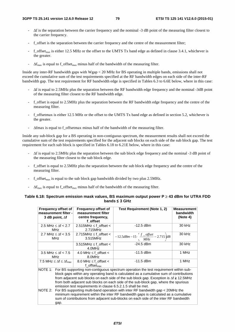
ETSI
ETSI TS 125 141 V12.6.0 (2015-01)793GPP TS 25.141 version 12.6.0 Release 12
- Δf is the separation between the carrier frequency and the nominal -3 dB point of the measuring filter closest to the carrier frequency.
- f_offset is the separation between the carrier frequency and the centre of the measurement filter;
- f_offsetmax is either 12.5 MHz or the offset to the UMTS Tx band edge as defined in clause 3.4.1, whichever is the greater.
- Δfmax is equal to f_offsetmax minus half of the bandwidth of the measuring filter.
Inside any inter-RF bandwidth gaps with Wgap < 20 MHz for BS operating in multiple bands, emissions shall not exceed the cumulative sum of the test requirements specified at the RF bandwidth edges on each side of the inter-RF bandwidth gap. The test requirement for RF bandwidth edge is specified in Tables 6.3 to 6.6E below, where in this case:
- Δf is equal to 2.5MHz plus the separation between the RF bandwidth edge frequency and the nominal -3dB point of the measuring filter closest to the RF bandwidth edge.
- f_offset is equal to 2.5MHz plus the separation between the RF bandwidth edge frequency and the centre of the measuring filter.
- f_offsetmax is either 12.5 MHz or the offset to the UMTS Tx band edge as defined in section 5.2, whichever is the greater.
- Δfmax is equal to f_offsetmax minus half of the bandwidth of the measuring filter.
Inside any sub-block gap for a BS operating in non-contiguous spectrum, the measurement results shall not exceed the cumulative sum of the test requirements specified for the adjacent sub blocks on each side of the sub block gap. The test requirement for each sub block is specified in Tables 6.18 to 6.21E below, where in this case:
- Δf is equal to 2.5MHz plus the separation between the sub block edge frequency and the nominal -3 dB point of the measuring filter closest to the sub block edge.
- f_offset is equal to 2.5MHz plus the separation between the sub block edge frequency and the centre of the measuring filter.
- f_offsetmax is equal to the sub block gap bandwidth divided by two plus 2.5MHz.
- Δfmax is equal to f_offsetmax minus half of the bandwidth of the measuring filter.
Table 6.18: Spectrum emission mask values, BS maximum output power P ≥ 43 dBm for UTRA FDD bands ≤ 3 GHz
Frequency offset of measurement filter -
3 dB point, Δf
Frequency offset of measurement filter centre frequency,
f_offset
Test Requirement (Note 1, 2) Measurement bandwidth
(Note 4)
2.5 MHz ≤ Δf < 2.7 MHz
2.515MHz ≤ f_offset < 2.715MHz
-12.5 dBm 30 kHz
2.7 MHz ≤ Δf < 3.5 MHz
2.715MHz ≤ f_offset < 3.515MHz dB
MHz
offsetfdBm ⎟
⎠
⎞⎜⎝
⎛ −⋅−− 715.2_
155.12 30 kHz
3.515MHz ≤ f_offset < 4.0MHz
-24.5 dBm 30 kHz
3.5 MHz ≤ Δf < 7.5 MHz
4.0 MHz ≤ f_offset < 8.0MHz
-11.5 dBm 1 MHz
7.5 MHz ≤ Δf ≤ Δfmax 8.0 MHz ≤ f_offset < f_offsetmax
-11.5 dBm 1 MHz
NOTE 1: For BS supporting non-contiguous spectrum operation the test requirement within sub-block gaps within any operating band is calculated as a cumulative sum of contributions from adjacent sub blocks on each side of the sub block gap. Exception is Δf ≥ 12.5MHz from both adjacent sub blocks on each side of the sub-block gap, where the spurious emission test requirements in clause 6.5.2.1.5 shall be met.
NOTE 2: For BS supporting multi-band operation with inter RF bandwidth gap < 20MHz the minimum requirement within the inter RF bandwidth gaps is calculated as a cumulative sum of contributions from adjacent sub-blocks on each side of the inter RF bandwidth gap.
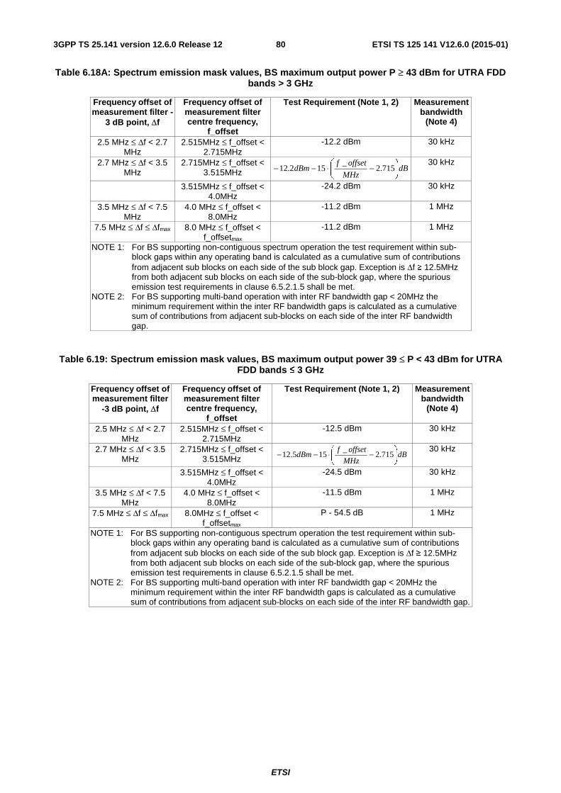
ETSI
ETSI TS 125 141 V12.6.0 (2015-01)803GPP TS 25.141 version 12.6.0 Release 12
Table 6.18A: Spectrum emission mask values, BS maximum output power P ≥ 43 dBm for UTRA FDD bands > 3 GHz
Frequency offset of measurement filter -
3 dB point, Δf
Frequency offset of measurement filter centre frequency,
f_offset
Test Requirement (Note 1, 2) Measurement bandwidth
(Note 4)
2.5 MHz ≤ Δf < 2.7 MHz
2.515MHz ≤ f_offset < 2.715MHz
-12.2 dBm 30 kHz
2.7 MHz ≤ Δf < 3.5 MHz
2.715MHz ≤ f_offset < 3.515MHz dB
MHz
offsetfdBm ⎟
⎠
⎞⎜⎝
⎛ −⋅−− 715.2_
152.12 30 kHz
3.515MHz ≤ f_offset < 4.0MHz
-24.2 dBm 30 kHz
3.5 MHz ≤ Δf < 7.5 MHz
4.0 MHz ≤ f_offset < 8.0MHz
-11.2 dBm 1 MHz
7.5 MHz ≤ Δf ≤ Δfmax 8.0 MHz ≤ f_offset < f_offsetmax
-11.2 dBm 1 MHz
NOTE 1: For BS supporting non-contiguous spectrum operation the test requirement within sub-block gaps within any operating band is calculated as a cumulative sum of contributions from adjacent sub blocks on each side of the sub block gap. Exception is Δf ≥ 12.5MHz from both adjacent sub blocks on each side of the sub-block gap, where the spurious emission test requirements in clause 6.5.2.1.5 shall be met.
NOTE 2: For BS supporting multi-band operation with inter RF bandwidth gap < 20MHz the minimum requirement within the inter RF bandwidth gaps is calculated as a cumulative sum of contributions from adjacent sub-blocks on each side of the inter RF bandwidth gap.
Table 6.19: Spectrum emission mask values, BS maximum output power 39 ≤ P < 43 dBm for UTRA FDD bands ≤ 3 GHz
Frequency offset of measurement filter
-3 dB point, Δf
Frequency offset of measurement filter centre frequency,
f_offset
Test Requirement (Note 1, 2) Measurement bandwidth
(Note 4)
2.5 MHz ≤ Δf < 2.7 MHz
2.515MHz ≤ f_offset < 2.715MHz
-12.5 dBm 30 kHz
2.7 MHz ≤ Δf < 3.5 MHz
2.715MHz ≤ f_offset < 3.515MHz dB
MHz
offsetfdBm ⎟
⎠
⎞⎜⎝
⎛ −⋅−− 715.2_
155.12 30 kHz
3.515MHz ≤ f_offset < 4.0MHz
-24.5 dBm 30 kHz
3.5 MHz ≤ Δf < 7.5 MHz
4.0 MHz ≤ f_offset < 8.0MHz
-11.5 dBm 1 MHz
7.5 MHz ≤ Δf ≤ Δfmax 8.0MHz ≤ f_offset < f_offsetmax
P - 54.5 dB 1 MHz
NOTE 1: For BS supporting non-contiguous spectrum operation the test requirement within sub-block gaps within any operating band is calculated as a cumulative sum of contributions from adjacent sub blocks on each side of the sub block gap. Exception is Δf ≥ 12.5MHz from both adjacent sub blocks on each side of the sub-block gap, where the spurious emission test requirements in clause 6.5.2.1.5 shall be met.
NOTE 2: For BS supporting multi-band operation with inter RF bandwidth gap < 20MHz the minimum requirement within the inter RF bandwidth gaps is calculated as a cumulative sum of contributions from adjacent sub-blocks on each side of the inter RF bandwidth gap.

ETSI
ETSI TS 125 141 V12.6.0 (2015-01)813GPP TS 25.141 version 12.6.0 Release 12
Table 6.19A: Spectrum emission mask values, BS maximum output power 39 ≤ P < 43 dBm for UTRA FDD bands > 3 GHz
Frequency offset of measurement filter
-3 dB point, Δf
Frequency offset of measurement filter centre frequency,
f_offset
Test Requirement (Note 1, 2) Measurement bandwidth
(Note 4)
2.5 MHz ≤ Δf < 2.7 MHz
2.515MHz ≤ f_offset < 2.715MHz
-12.2 dBm 30 kHz
2.7 MHz ≤ Δf < 3.5 MHz
2.715MHz ≤ f_offset < 3.515MHz dB
MHz
offsetfdBm ⎟
⎠
⎞⎜⎝
⎛ −⋅−− 715.2_
152.12 30 kHz
3.515MHz ≤ f_offset < 4.0MHz
-24.2 dBm 30 kHz
3.5 MHz ≤ Δf < 7.5 MHz
4.0 MHz ≤ f_offset < 8.0MHz
-11.2 dBm 1 MHz
7.5 MHz ≤ Δf ≤ Δfmax 8.0MHz ≤ f_offset < f_offsetmax
P - 54.2 dB 1 MHz
NOTE 1: For BS supporting non-contiguous spectrum operation the test requirement within sub-block gaps within any operating band is calculated as a cumulative sum of contributions from adjacent sub blocks on each side of the sub block gap. Exception is Δf ≥ 12.5MHz from both adjacent sub blocks on each side of the sub-block gap, where the spurious emission test requirements in clause 6.5.2.1.5 shall be met.
NOTE 2: For BS supporting multi-band operation with inter RF bandwidth gap < 20MHz the minimum requirement within the inter RF bandwidth gaps is calculated as a cumulative sum of contributions from adjacent sub-blocks on each side of the inter RF bandwidth gap.
Table 6.20: Spectrum emission mask values, BS maximum output power 31 ≤ P < 39 dBm for UTRA FDD bands ≤ 3 GHz
Frequency offset of measurement filter -
3 dB point,Δf
Frequency offset of measurement filter centre frequency,
f_offset
Test Requirement (Note 1, 2) Measurement bandwidth
(Note 4)
2.5 MHz ≤ Δf < 2.7 MHz 2.515MHz ≤ f_offset < 2.715MHz
P - 51.5 dB 30 kHz
2.7 MHz ≤ Δf < 3.5 MHz 2.715MHz ≤ f_offset < 3.515MHz dB
MHz
offsetfdBP ⎟
⎠
⎞⎜⎝
⎛ −⋅−− 715.2_
155.51
30 kHz
(Note 3) 3.515MHz ≤ f_offset < 4.0MHz
P - 63.5 dB 30 kHz
3.5 MHz ≤ Δf < 7.5 MHz 4.0 MHz ≤ f_offset < 8.0MHz
P - 50.5 dB 1 MHz
7.5 MHz ≤ Δf ≤ Δfmax 8.0MHz ≤ f_offset < f_offsetmax
P - 54.5 dB 1 MHz
NOTE 1: For BS supporting non-contiguous spectrum operation the test requirement within sub-block gaps within any operating band is calculated as a cumulative sum of contributions from adjacent sub blocks on each side of the sub block gap. Exception is Δf ≥ 12.5MHz from both adjacent sub blocks on each side of the sub-block gap, where the spurious emission test requirements in clause 6.5.2.1.5 shall be met.
NOTE 2: For BS supporting multi-band operation with inter RF bandwidth gap < 20MHz the minimum requirement within the inter RF bandwidth gaps is calculated as a cumulative sum of contributions from adjacent sub-blocks on each side of the inter RF bandwidth gap.

ETSI
ETSI TS 125 141 V12.6.0 (2015-01)823GPP TS 25.141 version 12.6.0 Release 12
Table 6.20A: Spectrum emission mask values, BS maximum output power 31 ≤ P < 39 dBm for UTRA FDD bands > 3 GHz
Frequency offset of measurement filter -
3 dB point,Δf
Frequency offset of measurement filter centre frequency,
f_offset
Test Requirement (Note 1, 2) Measurement bandwidth
(Note 4)
2.5 MHz ≤ Δf < 2.7 MHz 2.515MHz ≤ f_offset < 2.715MHz
P - 51.2 dB 30 kHz
2.7 MHz ≤ Δf < 3.5 MHz 2.715MHz ≤ f_offset < 3.515MHz dB
MHz
offsetfdBP ⎟
⎠
⎞⎜⎝
⎛ −⋅−− 715.2_
152.51 30 kHz
(Note 3) 3.515MHz ≤ f_offset < 4.0MHz
P - 63.2 dB 30 kHz
3.5 MHz ≤ Δf < 7.5 MHz 4.0 MHz ≤ f_offset < 8.0MHz
P - 50.2 dB 1 MHz
7.5 MHz ≤ Δf ≤ Δfmax 8.0MHz ≤ f_offset < f_offsetmax
P - 54.2 dB 1 MHz
NOTE 1: For BS supporting non-contiguous spectrum operation the test requirement within sub-block gaps within any operating band is calculated as a cumulative sum of contributions from adjacent sub blocks on each side of the sub block gap. Exception is Δf ≥ 12.5MHz from both adjacent sub blocks on each side of the sub-block gap, where the spurious emission test requirements in clause 6.5.2.1.5 shall be met.
NOTE 2: For BS supporting multi-band operation with inter RF bandwidth gap < 20MHz the minimum requirement within the inter RF bandwidth gaps is calculated as a cumulative sum of contributions from adjacent sub-blocks on each side of the inter RF bandwidth gap.
Table 6.21: Spectrum emission mask values, BS maximum output power P < 31 dBm for UTRA FDD bands ≤ 3 GHz
Frequency offset of measurement filter -
3 dB point, Δf
Frequency offset of measurement filter centre
frequency, f_offset
Test Requirement (Note 1, 2) Measurement bandwidth
(Note 4) 2.5 MHz ≤ Δf < 2.7
MHz 2.515MHz ≤ f_offset <
2.715MHz -20.5 dBm 30 kHz
2.7 ≤ Δf < 3.5 MHz 2.715MHz ≤ f_offset < 3.515MHz dB
MHz
offsetfdBm ⎟
⎠
⎞⎜⎝
⎛ −⋅−− 715.2_
155.20 30 kHz
(Note 3) 3.515MHz ≤ f_offset < 4.0MHz
-32.5 dBm 30 kHz
3.5 MHz ≤ Δf < 7.5 MHz
4.0 MHz ≤ f_offset < 8.0MHz -19.5 dBm 1 MHz
7.5 MHz ≤ Δf ≤ Δfmax 8.0MHz ≤ f_offset < f_offsetmax
-23.5 dBm 1 MHz
NOTE 1: For BS supporting non-contiguous spectrum operation the test requirement within sub-block gaps within any operating band is calculated as a cumulative sum of contributions from adjacent sub blocks on each side of the sub block gap. Exception is Δf ≥ 12.5MHz from both adjacent sub blocks on each side of the sub-block gap, where the spurious emission test requirements in clause 6.5.2.1.5 shall be met.
NOTE 2: For BS supporting multi-band operation with inter RF bandwidth gap < 20MHz the minimum requirement within the inter RF bandwidth gaps is calculated as a cumulative sum of contributions from adjacent sub-blocks on each side of the inter RF bandwidth gap.

ETSI
ETSI TS 125 141 V12.6.0 (2015-01)833GPP TS 25.141 version 12.6.0 Release 12
Table 6.21a: Spectrum emission mask values, BS maximum output power P < 31 dBm for UTRA FDD bands > 3 GHz
Frequency offset of measurement filter -
3 dB point, Δf
Frequency offset of measurement filter centre
frequency, f_offset
Test Requirement (Note 1, 2) Measurement bandwidth
(Note 4) 2.5 MHz ≤ Δf < 2.7
MHz 2.515MHz ≤ f_offset <
2.715MHz -20.2 dBm 30 kHz
2.7 ≤ Δf < 3.5 MHz 2.715MHz ≤ f_offset < 3.515MHz dB
MHz
offsetfdBm ⎟
⎠
⎞⎜⎝
⎛ −⋅−− 715.2_
152.20 30 kHz
(Note 3) 3.515MHz ≤ f_offset < 4.0MHz
-32.2 dBm 30 kHz
3.5 MHz ≤ Δf < 7.5 MHz
4.0 MHz ≤ f_offset < 8.0MHz -19.2 dBm 1 MHz
7.5 MHz ≤ Δf ≤ Δfmax 8.0MHz ≤ f_offset < f_offsetmax
-23.2 dBm 1 MHz
NOTE 1: For BS supporting non-contiguous spectrum operation the test requirement within sub-block gaps within any operating band is calculated as a cumulative sum of contributions from adjacent sub blocks on each side of the sub block gap. Exception is Δf ≥ 12.5MHz from both adjacent sub blocks on each side of the sub-block gap, where the spurious emission test requirements in clause 6.5.2.1.5 shall be met.
NOTE 2: For BS supporting multi-band operation with inter RF bandwidth gap < 20MHz the minimum requirement within the inter RF bandwidth gaps is calculated as a cumulative sum of contributions from adjacent sub-blocks on each side of the inter RF bandwidth gap.
For operation in band II, IV, V, X, XII, XIII, XIV, XXV and XXVI, the applicable additional requirement in Tables 6.21A, 6.21B or 6.21C apply in addition to the minimum requirements in Tables 6.18 to 6.21.
Table 6.21A: Additional spectrum emission limits for Bands II, IV, X, XXV
Frequency offset of measurement filter -3dB point,
Δf
Frequency offset of measurement filter centre frequency,
f_offset
Additional requirement
Measurement bandwidth
(Note 4)
2.5 MHz ≤ Δf < 3.5 MHz
2.515MHz ≤ f_offset < 3.515MHz
-15 dBm 30 kHz
3.5 MHz ≤ Δf ≤ Δfmax
4.0MHz ≤ f_offset < f_offsetmax
-13 dBm 1 MHz
Table 6.21B: Additional spectrum emission limits for Bands V, XXVI
Frequency offset of measurement filter -3dB point,
Δf
Frequency offset of measurement filter centre frequency,
f_offset
Additional requirement
Measurement bandwidth
(Note 4)
2.5 MHz ≤ Δf < 3.5 MHz
2.515MHz ≤ f_offset < 3.515MHz
-15 dBm 30 kHz
3.5 MHz ≤ Δf ≤ Δfmax
3.55MHz ≤ f_offset < f_offsetmax
-13 dBm 100 kHz
Table 6.21C: Additional spectrum emission limits for Bands XII, XIII, XIV
Frequency offset of measurement filter -3dB point,
Δf
Frequency offset of measurement filter centre frequency,
f_offset
Additional requirement
Measurement bandwidth
(Note 4)
2.5 MHz ≤ Δf < 2.6 MHz
2.515MHz ≤ f_offset < 2.615MHz
-13 dBm 30 kHz
2.6 MHz ≤ Δf ≤ Δfmax
2.65MHz ≤ f_offset < f_offsetmax
-13 dBm 100 kHz

ETSI
ETSI TS 125 141 V12.6.0 (2015-01)843GPP TS 25.141 version 12.6.0 Release 12
For Home BS, the applicable additional requirements in Tables 6.21D or 6.21E apply in addition to the minimum requirements in Tables 6.18 to 6.21.
Table 6.21D: Additional spectrum emission limit for Home BS, BS maximum output power 6 ≤ P ≤ 20 dBm for UTRA FDD bands ≤ 3 GHz
Frequency offset of measurement filter -3dB point,
Δf
Frequency offset of measurement filter centre frequency,
f_offset
Additional requirement
Measurement bandwidth
(Note 4)
12.5 MHz ≤ Δf ≤ Δfmax
13MHz ≤ f_offset < f_offsetmax
P – 54.5dBm 1 MHz
Table 6.21Da: Additional spectrum emission limit for Home BS, BS maximum output power 6 ≤ P ≤ 20 dBm for UTRA FDD bands > 3 GHz
Frequency offset of measurement filter -3dB point,
Δf
Frequency offset of measurement filter centre frequency,
f_offset
Additional requirement
Measurement bandwidth
(Note 4)
12.5 MHz ≤ Δf ≤ Δfmax
13MHz ≤ f_offset < f_offsetmax
P – 54.2dBm 1 MHz
Table 6.21E: Additional spectrum emission limit for Home BS, BS maximum output power P < 6 dBm for UTRA FDD bands ≤ 3 GHz
Frequency offset of measurement filter -3dB point,
Δf
Frequency offset of measurement filter centre frequency,
f_offset
Additional requirement
Measurement bandwidth
(Note 4)
12.5 MHz ≤ Δf ≤ Δfmax
13MHz ≤ f_offset < f_offsetmax
-48.5 dBm 1 MHz
Table 6.21Ea: Additional spectrum emission limit for Home BS, BS maximum output power P < 6 dBm for UTRA FDD bands > 3 GHz
Frequency offset of measurement filter -3dB point,
Δf
Frequency offset of measurement filter centre frequency,
f_offset
Additional requirement
Measurement bandwidth
(Note 4)
12.5 MHz ≤ Δf ≤ Δfmax
13MHz ≤ f_offset < f_offsetmax
-48.2 dBm 1 MHz
NOTE: If the above Test Requirement differs from the Minimum Requirement then the Test Tolerance applied
for this test is non-zero. The Test Tolerance for this test is defined in clause 4.2 and the explanation of how the Minimum Requirement has been relaxed by the Test Tolerance is given in Annex F.
In certain regions the following requirement may apply for protection of DTT. For UTRA BS operating in Band XX, the level of emissions in the band 470-790 MHz, measured in an 8MHz filter bandwidth on centre frequencies Ffilter according to Table 6.21F, shall not exceed the maximum emission level PEM,N declared by the manufacturer.
Table 6.21F: Declared emissions levels for protection of DTT
Filter centre frequency, Ffilter
Measurement bandwidth
Declared emission level [dBm]
Ffilter = 8*N + 306 (MHz); 21 ≤ N ≤ 60
8 MHz PEM,N

ETSI
ETSI TS 125 141 V12.6.0 (2015-01)853GPP TS 25.141 version 12.6.0 Release 12
NOTE: The regional requirement is defined in terms of EIRP (effective isotropic radiated power), which is dependent on both the BS emissions at the antenna connector and the deployment (including antenna gain and feeder loss). The requirement defined above provides the characteristics of the basestation needed to verify compliance with the regional requirement. Compliance with the regional requirement can be determined using the method outlined in Annex D of [1].
In certain regions, the following requirements may apply to UTRA BS operating in Band XXXII within 1452-1492 MHz. The level of unwanted emissions, measured on centre frequencies f_offset with filter bandwidth, according to Table 6.21G, shall neither exceed the maximum emission level PEM,B32,a , PEM,B32,b nor PEM,B32,c declared by the manufacturer.
Table 6.21G: Declared frequency band XXXII unwanted emission within 1452-1492 MHz
Frequency offset of measurement filter centre frequency, f_offset
Declared emission level [dBm]
Measurement bandwidth
5 MHz PEM,B32,a 5 MHz 10 MHz PEM,B32,b 5 MHz
15 MHz ≤ f_offset ≤ f_offsetmax, B32 PEM,B32,c 5 MHz NOTE: f_offsetmax, B32 denotes the frequency difference between the lower channel carrier
frequency and 1454.5 MHz, and the frequency difference between the upper channel carrier frequency and 1489.5 MHz for the set channel position.
NOTE: The regional requirement, included in [17], is defined in terms of EIRP per antenna, which is dependent on both the BS emissions at the antenna connector and the deployment (including antenna gain and feeder loss). The requirement defined above provides the characteristics of the base station needed to verify compliance with the regional requirement. The assessment of the EIRP level is described in Annex H of TS36.104 [15].
In certain regions, the following requirement may apply to UTRA BS operating in Band XXXII within 1452-1492MHz for the protection of services in spectrum adjacent to the frequency range 1452-1492 MHz. The level of emissions, measured on centre frequencies Ffilter with filter bandwidth according to Table 6.21H, shall neither exceed the maximum emission level PEM,B32,d nor PEM,B32,e declared by the manufacturer. This requirement applies in the frequency range 1429-1518MHz even though part of the range falls in the spurious domain.
Table 6.21H: Frequency band XXXII declared emission outside 1452-1492 MHz
Filter centre frequency, Ffilter Declared emission level [dBm]
Measurement bandwidth
1429.5 MHz ≤ Ffilter ≤ 1448.5 MHz PEM,B32,d 1 MHz Ffilter = 1450.5 MHz PEM,B32,e 3 MHz Ffilter = 1493.5 MHz PEM,B32,e 3 MHz
1495.5 MHz ≤ Ffilter ≤ 1517.5 MHz PEM,B32,d 1 MHz
NOTE: The regional requirement, included in [17], is defined in terms of EIRP, which is dependent on both the BS emissions at the antenna connector and the deployment (including antenna gain and feeder loss). The requirement defined above provides the characteristics of the base station needed to verify compliance with the regional requirement. The assessment of the EIRP level is described in Annex H of TS36.104 [15].
Notes for the Tables in this subclause:
NOTE 3: This frequency range ensures that the range of values of f_offset is continuous.
NOTE 4: As a general rule, the resolution bandwidth of the measuring equipment should be equal to the measurement bandwidth. However, to improve measurement accuracy, sensitivity and efficiency, the resolution bandwidth can be smaller than the measurement bandwidth. When the resolution bandwidth is smaller than the measurement bandwidth, the result should be integrated over the measurement bandwidth in order to obtain the equivalent noise bandwidth of the measurement bandwidth.

ETSI
ETSI TS 125 141 V12.6.0 (2015-01)863GPP TS 25.141 version 12.6.0 Release 12
6.5.2.2 Adjacent Channel Leakage power Ratio (ACLR)
6.5.2.2.1 Definition and applicability
Adjacent Channel Leakage power Ratio (ACLR) is the ratio of the RRC filtered mean power centered on the assigned channel frequency to the RRC filtered mean power centered on an adjacent channel frequency.
The requirements shall apply outside the BS RF bandwidth edges or maximum radio bandwidth edges whatever the type of transmitter considered (single carrier or multi-carrier). It applies for all transmission modes foreseen by the manufacturer's specification.
For a BS operating in non-contiguous spectrum, ACLR requirement also applies for the first adjacent channel, inside any sub-block gap with a gap size Wgap ≥ 15 MHz. The ACLR requirement for the second adjacent channel applies inside any sub-block gap with a gap size Wgap ≥ 20 MHz. The CACLR requirement in subclause 6.5.2.2.2 applies in sub block gaps for the frequency ranges defined in Table 6.23B.
For a BS operating in multiple bands, where multiple bands are mapped onto the same antenna connector, ACLR requirement also applies for the first adjacent channel, inside any inter RF bandwidth gap with a gap size Wgap ≥ 15 MHz. The ACLR requirement for the second adjacent channel applies inside any inter RF bandwidth gap with a gap size Wgap ≥ 20 MHz. The CACLR requirement in subclause 6.5.2.2.2 applies in inter RF bandwidth gaps for the frequency ranges defined in Table 6.23B.
6.5.2.2.2 Minimum Requirement
The minimum requirement is in TS 25.104 [1] clause 6.6.2.2
Table 6.22: (void)
6.5.2.2.3 Test purpose
To verify that the adjacent channel leakage power ratio requirement shall be met as specified by the minimum requirement.
6.5.2.2.4 Method of test
6.5.2.2.4.1 Initial conditions
Test environment: normal; see clause 4.4.1.
RF channels to be tested for single carrier: B, M and T; see clause 4.8
RF bandwidth positions to be tested for multi-carrier: BRFBW, MRFBW and TRFBW in single band operation; BRFBW_T"RFBW and B"RFBW_TRFBW in multi-band operation; see subclause 4.8.1.
1) Connect measurement device to the base station antenna connector as shown in annex B.
2) The measurement device characteristics shall be:
- measurement filter bandwidth: defined in clause 6.5.2.2.1;
- detection mode: true RMS voltage or true average power.
3) Set the base station to transmit a signal modulated in accordance to TM1, clause 6.1.1.1, at manufacturer"s declared rated output power, PRAT.
For a BS declared to be capable of multi-carrier operation, set the base station to transmit according to TM1 on all carriers configured using the applicable test configuration and corresponding power setting specified in sub-clause 4.12.
4) Set carrier frequency within the frequency band supported by BS. Minimum carrier spacing shall be 5 MHz and maximum carrier spacing shall be specified by manufacturer.

ETSI
ETSI TS 125 141 V12.6.0 (2015-01)873GPP TS 25.141 version 12.6.0 Release 12
6.5.2.2.4.2 Procedure
1) Measure Adjacent channel leakage power ratio for 5 MHz and 10 MHz offsets both side of channel frequency. In multiple carrier case only offset frequencies below the lowest and above the highest carrier frequency used shall be measured.
2) For the ACLR requirement applied inside sub-block gap for non-contiguous spectrum operation or inside inter RF bandwidth gap for multi-band operation:
a) Measure ACLR inside sub-block gap or inter RF bandwidth gap as specified in clause 6. 5.2.2.5, if applicable.
b) Measure Cumulative Adjacent Channel Leakage power Ratio (CACLR) inside sub-block gap or inter RF bandwidth gap as specified in clause 6. 5.2.2.6, if applicable.
In addition, for a multi-band capable BS, the following steps shall apply:
3) For multi-band capable BS and single band tests, repeat the steps above per involved band where single band test configurations and test models shall apply with no carrier activated in the other band.
4) For multi-band capable BS with separate antenna connector, the antenna connector not being under test in case of single-band or multi-band test shall be terminated.
6.5.2.2.5 Test Requirement
For Category A Wide Area BS, either the ACLR limits in the tables below or the absolute limit of -13dBm/MHz apply, whichever is less stringent.
For Category B Wide Area BS, either the ACLR limits in the tables below or the absolute limit of -15dBm/MHz apply, whichever is less stringent.
For Medium Range BS, either the ACLR limits in the tables below or the absolute limit of -25 dBm/MHz shall apply, whichever is less stringent.
For Local Area BS, either the ACLR limits in the tables below or the absolute limit of -32dBm/MHz shall apply, whichever is less stringent.
The measurement result in step 1 of 6.5.2.2.4.2 shall not be less than the ACLR limit specified in tables 6.23
Table 6.23: BS ACLR
BS channel offset below the first or above the last carrier frequency used
ACLR limit
5 MHz 44.2 dB 10 MHz 49.2 dB
Note 1: In certain regions, the adjacent channel power (the RRC filtered mean power centered on an adjacent channel frequency) shall be less than or equal to -7.2 dBm/3.84 MHz (for Band I, III, IX, XI and XXI) or +2.8 dBm/3.84MHz (for Band VI, VIII and XIX) or as specified by the ACLR limit, whichever is the higher. This note is not applicable for Home BS.
Note 2: For Home BS, the adjacent channel power (the RRC filtered mean power centered on an adjacent channel frequency) shall be less than or equal to -42.7 dBm/3.84MHz f≤ 3.0 GHz and -42.4 dBm/3.84MHz for 3.0 GHz < f ≤ 4.2 GHz or as specified by the ACLR limit, whichever is the higher.
NOTE: If the above Test Requirement differs from the Minimum Requirement then the Test Tolerance applied for this test is non-zero. The Test Tolerance for this test is defined in clause 4.2 and the explanation of how the Minimum Requirement has been relaxed by the Test Tolerance is given in Annex F.
The measurement result in step 2a of 6.5.2.2.4.2 shall not be less than the ACLR limit specified in table 6.23A

ETSI
ETSI TS 125 141 V12.6.0 (2015-01)883GPP TS 25.141 version 12.6.0 Release 12
Table 6.23A: BS ACLR in non-contiguous spectrum or multiple bands
Sub-block or inter RF bandwidth gap size (Wgap) where the limit applies
BS adjacent channel centre frequency offset below or
above the sub-block edge or the RF bandwidth edge
(inside the gap)
Assumed adjacent channel carrier
(informative)
Filter on the adjacent channel frequency and
corresponding filter bandwidth
ACLR limit
Wgap ≥ 15 MHz 2.5 MHz 3.84 Mcps UTRA RRC (3.84 Mcps) 44.2 dB Wgap ≥ 20 MHz 7.5 MHz 3.84 Mcps UTRA RRC (3.84 Mcps) 44.2 dB
NOTE: The RRC filter shall be equivalent to the transmit pulse shape filter defined in TS 25.104, with a chip rate as defined in this table.
6.5.2.2.6 Cumulative ACLR test requirement in non-contiguous spectrum or multiple-bands
The following test requirement applies for a BS operating in non-contiguous spectrum or multiple bands.
The following requirement applies for the gap sizes listed in Table 6.23B,
- inside a sub-block gap within an operating band for a BS operating in non-contiguous spectrum;
- inside an inter-RF bandwidth gap for a BS capable of multi-band operation, where multiple bands are mapped on the same antenna connector.
The Cumulative Adjacent Channel Leakage power Ratio (CACLR) in a sub-block gap or inter-RF bandwidth gap is the ratio of
a) the sum of the filtered mean power centred on the assigned channel frequencies for the two carriers adjacent to each side of the sub-block gap or inter-RF bandwidth gap, and
b) the filtered mean power centred on a frequency channel adjacent to one of the respective sub-block edges or RF bandwidth edges.
The assumed filter for the adjacent channel frequency is defined in Table 6.23B and the filters on the assigned channels are defined in Table 6.23C.
For Wide Area Category A BS, either the CACLR limits in Table 6.23B or the absolute limit of -13dBm/MHz apply, whichever is less stringent.
For Wide Area Category B BS, either the CACLR limits in Table 6.23B or the absolute limit of -15dBm/MHz apply, whichever is less stringent.
For Medium Range BS, either the CACLR limits in Table 6.23B or the absolute limit of -25 dBm/MHz shall apply, whichever is less stringent.
For Local Area BS, either the CACLR limits in Table 6.23B or the absolute limit of -32 dBm/MHz shall apply, whichever is less stringent.
The CACLR for UTRA carriers located on either side of the sub-block gap or inter-RF bandwidth gap shall be higher than the value specified in Table 6.23B.
Table 6.23B: Base Station CACLR in non-contiguous spectrum or multiple bands
Sub-block or inter-RF bandwidth gap size (Wgap) where the limit applies
BS adjacent channel centre frequency offset below or
above the sub-block edge or the RF bandwidth edge
(inside the gap)
Assumed adjacent channel carrier
(informative)
Filter on the adjacent channel frequency and
corresponding filter bandwidth
CACLR limit
5 MHz ≤ Wgap < 15 MHz
2.5 MHz 3.84 Mcps UTRA RRC (3.84 Mcps) 44.2 dB
10 MHz < Wgap < 20 MHz
7.5 MHz 3.84 Mcps UTRA RRC (3.84 Mcps) 44.2 dB
NOTE: The RRC filter shall be equivalent to the transmit pulse shape filter defined in TS 25.104, with a chip rate as defined in this table.

ETSI
ETSI TS 125 141 V12.6.0 (2015-01)893GPP TS 25.141 version 12.6.0 Release 12
Table 6.23C: Filter parameters for the assigned channel
RAT of the carrier adjacent to the sub-block or inter-RF
bandwidth gap
Filter on the assigned channel frequency and corresponding filter bandwidth
UTRA FDD RRC (3.84 Mcps) NOTE: The RRC filter shall be equivalent to the transmit pulse shape filter
defined in TS 25.104,with a chip rate as defined in this table.
6.5.3 Spurious emissions
6.5.3.1 Definition and applicability
Spurious emissions are emissions which are caused by unwanted transmitter effects such as harmonics emission, parasitic emission, intermodulation products and frequency conversion products, but exclude out of band emissions. This is measured at the base station antenna connector.
The requirements (except 6.5.3.7.6 and 6.5.3.7.9 and specifically stated exceptions in Table 6.38) apply at frequencies within the specified frequency ranges, which are more than 12.5 MHz under the first carrier frequency used or more than 12.5 MHz above the last carrier frequency used.
The requirements shall apply whatever the type of transmitter considered (single carrier or multi-carrier). It applies for all transmission modes foreseen by the manufacturer's specification.
For BS capable of multi-band operation where multiple bands are mapped on the same antenna connector, the requirements (except 6.5.3.7.6 and 6.5.3.7.9 and specifically stated exceptions in Table 6.38) apply at frequencies within the specified frequency ranges, excluding the frequency ranges which are less than or equal to 12.5MHz below the first carrier frequency used and less than or equal to 12.5MHz above the last carrier frequency used for each supported operating band. For BS capable of multi-band operation where multiple bands are mapped on separate antenna connectors, the single-band requirements apply and the multi-band exclusions and provisions are not applicable.
Unless otherwise stated, all requirements are measured as mean power (RMS).
6.5.3.2 (void)
6.5.3.3 (void)
6.5.3.4 Minimum Requirements
The minimum requirements are in TS 25.104 [1] clause 6.6.3.

ETSI
ETSI TS 125 141 V12.6.0 (2015-01)903GPP TS 25.141 version 12.6.0 Release 12
Table 6.24: (void)
Table 6.25: (void)
Table 6.25A: (void)
Table 6.25B: (void)
Table 6.25C: (void)
Table 6.25D: (void)
Table 6.25E: (void)
Table 6.26: (void)
Table 6.26A: (void)
Table 6.26B: (void)
Table 6.27: (void)
Table 6.28: (void)
Table 6.29: (void)
Table 6.30: (void)
Table 6.31: (void)
Table 6.32: (void)
Table 6.33: (void)
Table 6.34: (void)
6.5.3.5 Test purpose
This test measures conducted spurious emission from the BS transmitter antenna connector, while the transmitter is in operation.
6.5.3.6 Method of Test
6.5.3.6.1 Initial conditions
Test environment: normal; see clause 4.4.1.
RF channels to be tested for single carrier: B, M and T; see clause 4.8
RF bandwidth positions to be tested for multi-carrier: BRFBW, MRFBW and TRFBW in single band operation; BRFBW_T"RFBW and B"RFBW_TRFBW in multi-band operation; see subclause 4.8.1.
1) Connect the BS antenna connector to a measurement receiver using an attenuator or a directional coupler if necessary
2) Measurements shall use a measurement bandwidth in accordance to the tables in section 6.5.3.4.
3) Detection mode: True RMS.

ETSI
ETSI TS 125 141 V12.6.0 (2015-01)913GPP TS 25.141 version 12.6.0 Release 12
6.5.3.6.2 Procedure
1) For a BS declared to be capable of single carrier operation only, set the base station to transmit a signal according to TM1, clause 6.1.1.1 at the manufacturer"s declared rated output power, PRAT.
For a BS declared to be capable of multi-carrier operation, set the base station to transmit according to TM1 on all carriers configured using the applicable test configuration and corresponding power setting specified in sub-clause 4.12.
2) Measure the emission at the specified frequencies with specified measurement bandwidth and note that the measured value does not exceed the specified value.
In addition, for a multi-band capable BS, the following steps shall apply:
3) For multi-band capable BS and single band tests, repeat the steps above per involved band where single band test configurations and test models shall apply with no carrier activated in the other band.
4) For multi-band capable BS with separate antenna connector, the antenna connector not being under test in case of single-band or multi-band test shall be terminated.
6.5.3.7 Test requirements
The measurement result in step 2 of 6.5.3.6.2 shall not exceed the maximum level specified in tables 6.35 to 6.47 if applicable for the BS under test.
NOTE: If a Test Requirement in this section differs from the corresponding Minimum Requirement then the Test Tolerance applied for this test is non-zero. The Test Tolerance for this test is defined in clause 4.2 and the explanation of how the Minimum Requirement has been relaxed by the Test Tolerance is given in Annex F.
6.5.3.7.1 Spurious emissions (Category A)
The following requirements shall be met in cases where Category A limits for spurious emissions, as defined in ITU-R Recommendation SM.329 [4], are applied.
Table 6.35: BS Mandatory spurious emissions limits, Category A
Band Maximum level Measurement Bandwidth
Notes
9 kHz to 150 kHz
-13 dBm
1 kHz Note 1 150 kHz to 30 MHz 10 kHz Note 1 30 MHz to 1 GHz 100 kHz Note 1
1 GHz to 12,75 GHz 1 MHz Note 2 12.75 GHz - 5th harmonic of the upper frequency edge of the DL
operating band in GHz
1 MHz Note 2, Note 3
NOTE 1: Bandwidth as in ITU-R SM.329 [4], clause 4.1 NOTE 2: Upper frequency as in ITU-R SM.329 [4], clause 2.5 Table 1 NOTE 3: Applies only for Band XXII
6.5.3.7.2 Spurious emissions (Category B)
The following requirements shall be met in cases where Category B limits for spurious emissions, as defined in ITU-R Recommendation SM.329[4], are applied.

ETSI
ETSI TS 125 141 V12.6.0 (2015-01)923GPP TS 25.141 version 12.6.0 Release 12
Table 6.36: BS Mandatory spurious emissions limits, operating band I, II, III, IV, VII, X, XXV, XXXII (Category B)
Band Maximum Level
Measurement Bandwidth
Note
9 kHz ↔ 150 kHz -36 dBm 1 kHz Note 1 150 kHz ↔ 30 MHz -36 dBm 10 kHz Note 1 30 MHz ↔ 1 GHz -36 dBm 100 kHz Note 1
1 GHz ↔ Flow - 10 MHz -30 dBm 1 MHz Note 1 Flow - 10 MHz ↔ Fhigh + 10 MHz -15 dBm 1 MHz Note 2
Fhigh + 10 MHz ↔ 12.75 GHz -30 dBm 1 MHz Note 3 12.75 GHz - 5th harmonic of the upper frequency edge of the DL
operating band in GHz
-30 dBm 1 MHz Note 3, Note 4
NOTE 1: Bandwidth as in ITU-R Recommendation SM.329 [4], s4.1 NOTE 2: Limit based on ITU-R Recommendation SM.329 [4], s4.3 and Annex 7 NOTE 3: Bandwidth as in ITU-R Recommendation SM.329 [4], s4.1. Upper frequency as in ITU-R
SM.329 [4], s2.5 table 1 NOTE 4: Applies only for Band XXII Key: Flow: The lowest downlink frequency of the operating band as defined in Table 3.0. Fhigh: The highest downlink frequency of the operating band as defined in Table 3.0.
Table 6.36A: BS Mandatory spurious emissions limits, operating band V, VIII, XII, XIII, XIV, XX, XXVI (Category B)
Band Maximum Level
Measurement Bandwidth
Note
9 kHz ↔ 150 kHz -36 dBm 1 kHz Note 1 150 kHz ↔ 30 MHz -36 dBm 10 kHz Note 1
30 MHz ↔ Flow - 10 MHz -36 dBm 100 kHz Note 1 Flow - 10 MHz ↔ Fhigh + 10 MHz -16 dBm 100 kHz Note 2
Fhigh + 10 MHz ↔ 1 GHz -36 dBm 100 kHz Note 1 1GHz ↔ 12.75GHz -30 dBm 1 MHz Note 3
NOTE 1: Bandwidth as in ITU-R Recommendation SM.329 [4], s4.1 NOTE 2: Limit based on ITU-R Recommendation SM.329 [4], s4.3 and Annex 7 NOTE 3: Bandwidth as in ITU-R Recommendation SM.329 [4], s4.1. Upper frequency as in ITU-R
SM.329 [4], s2.5 table 1 Key: Flow: The lowest downlink frequency of the operating band as defined in Table 3.0. Fhigh: The highest downlink frequency of the operating band as defined in Table 3.0.
Table 6.36B: (void)
Table 6.36C: (void)
Table 6.36D: (void)
Table 6.36E: (void)
Table 6.36F: (void)
Table 6.36G: (void)
6.5.3.7.3 Protection of the BS receiver of own or different BS
This requirement shall be applied in order to prevent the receivers of the BS being desensitised by emissions from a BS transmitter. This is measured at the transmit antenna port for any type of BS which has common or separate Tx/Rx antenna ports.

ETSI
ETSI TS 125 141 V12.6.0 (2015-01)933GPP TS 25.141 version 12.6.0 Release 12
Table 6.37: Wide Area BS Spurious emissions limits for protection of the BS receiver
Operating Band
Band Maximum Level
Measurement Bandwidth
Note
I 1920 - 1980MHz -96 dBm 100 kHz II 1850 - 1910 MHz -96 dBm 100 kHz III 1710 - 1785 MHz -96 dBm 100 kHz IV 1710 - 1755 MHz -96 dBm 100 kHz V 824 - 849 MHz -96 dBm 100 kHz
VI, XIX 815 - 845 MHz -96 dBm 100 kHz VII 2500 - 2570 MHz -96 dBm 100 kHz VIII 880-915 MHz -96 dBm 100 kHz IX 1749.9 - 1784.9 MHz -96 dBm 100 kHz X 1710 - 1770 MHz -96 dBm 100 kHz XI 1427.9 - 1447.9 MHz -96 dBm 100 kHz XII 699 - 716 MHz -96 dBm 100 kHz XIII 777 - 787 MHz -96 dBm 100 kHz XIV 788 - 798 MHz -96 dBm 100 kHz XX 832 - 862 MHz -96 dBm 100 kHz XXI 1447.9 - 1462.9 MHz -96 dBm 100 kHz XXII 3410 – 3490 MHz -96 dBm 100 kHz XXV 1850-1915 MHz -96 dBm 100 kHz XXVI 814-849 MHz -96 dBm 100 kHz
Table 6.37A: Medium Range BS Spurious emissions limits for protection of the BS receiver
Operating Band
Band Maximum Level
Measurement Bandwidth
Note
I 1920 - 1980MHz -86 dBm 100 kHz II 1850 - 1910 MHz -86 dBm 100 kHz III 1710 - 1785 MHz -86 dBm 100 kHz IV 1710 - 1755 MHz -86 dBm 100 kHz V 824 - 849 MHz -86 dBm 100 kHz
VI, XIX 815 - 845 MHz -86 dBm 100 kHz VII 2500 - 2570 MHz -86 dBm 100 kHz VIII 880-915 MHz -86 dBm 100 kHz IX 1749.9 - 1784.9 MHz -86 dBm 100 kHz X 1710 - 1770 MHz -86 dBm 100 kHz XI 1427.9 - 1447.9 MHz -86 dBm 100 kHz XII 699 - 716 MHz -86 dBm 100 kHz XIII 777 - 787 MHz -86 dBm 100 kHz XIV 788 - 798 MHz -86 dBm 100 kHz XX 832 - 862 MHz -86 dBm 100 kHz XXI 1447.9 - 1462.9 MHz -86 dBm 100 kHz XXII 3410 – 3490 MHz -86 dBm 100 kHz XXV 1850-1915 MHz -86 dBm 100 kHz XXVI 814-849 MHz -86 dBm 100 kHz

ETSI
ETSI TS 125 141 V12.6.0 (2015-01)943GPP TS 25.141 version 12.6.0 Release 12
Table 6.37B: Local Area BS Spurious emissions limits for protection of the BS receiver
Operating Band
Band Maximum Level
Measurement Bandwidth
Note
I 1920 - 1980MHz -82 dBm 100 kHz II 1850 - 1910 MHz -82 dBm 100 kHz III 1710 - 1785 MHz -82 dBm 100 kHz IV 1710 - 1755 MHz -82 dBm 100 kHz V 824 - 849 MHz -82 dBm 100 kHz
VI, XIX 815 - 845 MHz -82 dBm 100 kHz VII 2500 - 2570 MHz -82 dBm 100 kHz VIII 880-915 MHz -82 dBm 100 kHz IX 1749.9 - 1784.9 MHz -82 dBm 100 kHz X 1710 - 1770 MHz -82 dBm 100 kHz XI 1427.9 - 1447.9 MHz -82 dBm 100 kHz XII 699 - 716 MHz -82 dBm 100 kHz XIII 777 - 787 MHz -82 dBm 100 kHz XIV 788 - 798 MHz -82 dBm 100 kHz XX 832 - 862 MHz -82 dBm 100 kHz XXI 1447.9 - 1462.9 MHz -82 dBm 100 kHz XXII 3410 – 3490 MHz -82 dBm 100 kHz XXV 1850-1915 MHz -82 dBm 100 kHz XXVI 814-849 MHz -82 dBm 100 kHz
Table 6.37C: Home BS Spurious emissions limits for protection of the BS receiver
Operating Band
Band Maximum Level
Measurement Bandwidth
Note
I 1920 - 1980MHz -82 dBm 100 kHz II 1850-1910 MHz -82 dBm 100 kHz III 1710-1785 MHz -82 dBm 100 kHz IV 1710-1755 MHz -82 dBm 100 kHz V 824-849 MHz -82 dBm 100 kHz
VI, XIX 815-845 MHz -82 dBm 100 kHz VII 2500-2570 MHz -82 dBm 100 kHz VIII 880-915 MHz -82 dBm 100 kHz IX 1749.9-1784.9 MHz -82 dBm 100 kHz X 1710-1770 MHz -82 dBm 100 kHz XI 1427.9 - 1447.9 MHz -82 dBm 100 kHz XII 699 - 716 MHz -82 dBm 100 kHz XIII 777 - 787 MHz -82 dBm 100 kHz XIV 788 - 798 MHz -82 dBm 100 kHz XX 832 - 862 MHz -82 dBm 100 kHz XXI 1447.9 - 1462.9 MHz -82 dBm 100 kHz XXII 3410 – 3490 MHz -82 dBm 100 kHz XXV 1850-1915 MHz -82 dBm 100 kHz XXVI 814-849 MHz -82 dBm 100 kHz
6.5.3.7.4 Co-existence with other systems in the same geographical area
These requirements may be applied for the protection of UE, MS and/or BS operating in other frequency bands in the same geographical area. The requirements may apply in geographic areas in which both a UTRA FDD BS and a system operating in another frequency band than the FDD operating band are deployed. The system operating in the other frequency band may be GSM, DCS, PCS, CDMA, E-UTRA and/or UTRA.

ETSI
ETSI TS 125 141 V12.6.0 (2015-01)953GPP TS 25.141 version 12.6.0 Release 12
The power of any spurious emission shall not exceed the limits of Table 6.38 for a BS where requirements for co-existence with the system listed in the first column apply. For BS capable of multi-band operation, the exclusions and conditions in the Note column of Table 6.38 apply for each supported operating band. For BS capable of multi-band operation where multiple bands are mapped on separate antenna connectors, the exclusions and conditions in the Note column of Table 6.38 apply for the operating band supported at that antenna connector.
Table 6.38: BS Spurious emissions limits for UTRA FDD BS in geographic coverage area of systems operating in other frequency bands
System type operating in
the same geographical
area
Band for co-existence
requirement
Maximum Level
Measurement Bandwidth
Note
GSM900 921 - 960 MHz -57 dBm 100 kHz This requirement does not apply to UTRA FDD operating in band VIII
876 - 915 MHz -61 dBm 100 kHz For the frequency range 880-915 MHz, this requirement does not apply to UTRA FDD operating in band VIII, since it is already covered by the requirement in sub-clause 6.5.3.7.3.
DCS1800 1805 - 1880 MHz -47 dBm 100 kHz This requirement does not apply to UTRA FDD operating in band III
1710 - 1785 MHz -61 dBm 100 kHz This requirement does not apply to UTRA FDD operating in band III, since it is already covered by the requirement in sub-clause 6.5.3.7.3 .
PCS1900 1930 - 1990 MHz -47 dBm 100 kHz This requirement does not apply to UTRA FDD BS operating in frequency band II or band XXV
1850 - 1910 MHz -61 dBm 100 kHz This requirement does not apply to UTRA FDD BS operating in frequency band II or band XXV, since it is already covered by the requirement in sub-clause 6.5.3.7.3.
GSM850 or CDMA850
869 - 894 MHz -57 dBm 100 kHz This requirement does not apply to UTRA FDD BS operating in frequency band V or XXVI
824 - 849 MHz -61 dBm 100 kHz This requirement does not apply to UTRA FDD BS operating in frequency band V or XXVI, since it is already covered by the requirement in sub-clause 6.5.3.7.3.
UTRA FDD Band I or E-UTRA Band 1
2110 - 2170 MHz -52 dBm 1 MHz This requirement does not apply to UTRA FDD BS operating in band I,
1920 - 1980 MHz -49 dBm 1 MHz This requirement does not apply to UTRA FDD BS operating in band I, since it is already covered by the requirement in sub-clause 6.5.3.7.3 .
UTRA FDD Band II or E-UTRA Band 2
1930 - 1990 MHz -52 dBm 1 MHz This requirement does not apply to UTRA FDD BS operating in band II or band XXV
1850 - 1910 MHz -49 dBm 1 MHz This requirement does not apply to UTRA FDD BS operating in band II or band XXV, since it is already covered by the requirement in sub-clause 6.5.3.7.3.
UTRA FDD Band III or E-UTRA Band 3
1805 - 1880 MHz -52 dBm 1 MHz This requirement does not apply to UTRA FDD BS operating in band III or band IX
1710 - 1785 MHz -49 dBm 1 MHz This requirement does not apply to UTRA FDD BS operating in band III, since it is already covered by the requirement in sub-clause 6.5.3.7.3 . For UTRA BS operating in band IX, it applies for 1710 MHz to 1749.9 MHz and 1784.9 MHz to 1785 MHz, while the rest is covered in sub-clause 6.5.3.7.3.
UTRA FDD Band IV or E-UTRA Band 4
2110 - 2155 MHz -52 dBm 1 MHz This requirement does not apply to UTRA FDD BS operating in band IV or band X
1710 - 1755 MHz -49 dBm 1 MHz This requirement does not apply to UTRA FDD BS operating in band IV or band X, since it is already covered by the requirement in sub-clause 6.5.3.7.3 .

ETSI
ETSI TS 125 141 V12.6.0 (2015-01)963GPP TS 25.141 version 12.6.0 Release 12
UTRA FDD Band V or E-UTRA Band 5
869 - 894 MHz -52 dBm 1 MHz This requirement does not apply to UTRA FDD BS operating in band V or XXVI
824 - 849 MHz -49 dBm 1 MHz This requirement does not apply to UTRA FDD BS operating in band V or XXVI, since it is already covered by the requirement in sub-clause 6.5.3.7.3 .
UTRA FDD Band VI or
XIX, or E-UTRA
Band 6, 18 or 19
860 - 890 MHz -52 dBm 1 MHz This requirement does not apply to UTRA FDD BS operating in band VI or XIX
815 - 845 MHz -49 dBm 1 MHz This requirement does not apply to UTRA FDD BS operating in band VI or XIX, since it is already covered by the requirement in sub-clause 6.5.3.7.3 .
UTRA FDD Band VII or
E-UTRA Band 7
2620 - 2690 MHz -52 dBm 1 MHz This requirement does not apply to UTRA FDD BS operating in band VII,
2500 - 2570 MHz -49 dBm 1 MHz This requirement does not apply to UTRA FDD BS operating in band VII, since it is already covered by the requirement in sub-clause 6.5.3.7.3 .
UTRA FDD Band VIII or
E-UTRA Band 8
925 - 960 MHz -52 dBm 1 MHz This requirement does not apply to UTRA FDD BS operating in band VIII.
880 - 915 MHz -49 dBm 1 MHz This requirement does not apply to UTRA FDD BS operating in band VIII, since it is already covered by the requirement in sub-clause 6.5.3.7.3.
UTRA FDD Band IX or E-UTRA Band 9
1844.9 - 1879.9 MHz
-52 dBm 1 MHz This requirement does not apply to UTRA FDD BS operating in band III or band IX
1749. 9 - 1784.9 MHz
-49 dBm 1 MHz This requirement does not apply to UTRA FDD BS operating in band III or band IX, since it is already covered by the requirement in sub-clause 6.5.3.7.3 .
UTRA FDD Band X or E-UTRA Band 10
2110 - 2170 MHz -52 dBm 1 MHz This requirement does not apply to UTRA FDD BS operating in band IV or band X
1710 - 1770 MHz -49 dBm 1 MHz This requirement does not apply to UTRA FDD BS operating in band X, since it is already covered by the requirement in sub-clause 6.5.3.7.3. For UTRA FDD BS operating in Band IV, it applies for 1755 MHz to 1770 MHz, while the rest is covered in sub-clause 6.5.3.7.3.
UTRA FDD Band XI or
XXI or E-UTRA
Band 11 or 21
1475.9 - 1510.9 MHz
-52 dBm 1 MHz This requirement does not apply to UTRA FDD BS operating in band XI, XXI, or XXXII.
1427.9 - 1447.9 MHz
-49 dBm 1 MHz This requirement does not apply to UTRA FDD BS operating in band XI, since it is already covered by the requirement in sub-clause 6.5.3.7.3. For UTRA BS operating in band XXXII, this requirement applies for carriers allocated within 1475.9MHz and 1495.9MHz.
1447.9 - 1462.9 MHz
-49 dBm 1 MHz This requirement does not apply to UTRA FDD BS operating in band XXI, since it is already covered by the requirement in sub-clause 6.5.3.7.3. For UTRA BS operating in band XXXII, this requirement applies for carriers allocated within 1475.9MHz and 1495.9MHz.
UTRA FDD Band XII or
E-UTRA Band 12
729 - 746 MHz -52 dBm 1 MHz This requirement does not apply to UTRA FDD BS operating in band XII
699 - 716 MHz -49 dBm 1 MHz This requirement does not apply to UTRA FDD BS operating in band XII, since it is already covered by the requirement in sub-clause 6.5.3.7.3.
UTRA FDD Band XIII or
E-UTRA Band 13
746 - 756 MHz -52 dBm 1 MHz This requirement does not apply to UTRA FDD BS operating in band XIII
777 - 787 MHz -49 dBm 1 MHz This requirement does not apply to UTRA FDD BS operating in band XIII, since it is already covered by the requirement in sub-clause 6.5.3.7.3.
UTRA FDD Band XIV or
758 - 768 MHz -52 dBm 1 MHz This requirement does not apply to UTRA FDD BS operating in band XIV

ETSI
ETSI TS 125 141 V12.6.0 (2015-01)973GPP TS 25.141 version 12.6.0 Release 12
E-UTRA Band 14
788 - 798 MHz -49 dBm 1 MHz This requirement does not apply to UTRA FDD BS operating in band XIV, since it is already covered by the requirement in sub-clause 6.5.3.7.3.
E-UTRA Band 17
734 - 746 MHz -52 dBm 1 MHz This requirement does not apply to UTRA FDD BS operating in band XII
704 - 716 MHz -49 dBm 1 MHz This requirement does not apply to UTRA FDD BS operating in band XII, since it is already covered by the requirement in sub-clause 6.6.3.2.
UTRA FDD Band XX or
E-UTRA Band 20
791 - 821 MHz -52 dBm 1 MHz This requirement does not apply to UTRA FDD BS operating in band XX
832 - 862 MHz -49 dBm 1 MHz This requirement does not apply to UTRA FDD BS operating in band XX, since it is already covered by the requirement in sub-clause 6.6.3.2.
UTRA FDD Band XXII or
E-UTRA Band 22
3510 -3590 MHz -52 dBm 1 MHz This requirement does not apply to UTRA FDD BS operating in band XXII
3410 -3490 MHz -49 dBm 1 MHz This requirement does not apply to UTRA FDD BS operating in band XXII, since it is already covered by the requirement in sub-clause 6.5.3.7.3.
E-UTRA Band 23
2180 - 2200 MHz -52 dBm 1 MHz
2000 - 2020 MHz -49 dBm 1 MHz This requirement does not apply to UTRA FDD BS operating in Band II or XXV, where the limits are defined separately.
2000 – 2010 MHz -30 dBm 1 MHz This requirement only applies to UTRA FDD BS operating in Band II or Band XXV. This requirement applies starting 5 MHz above the Band XXV downlink operating band. (Note 3)
2010 – 2020 MHZ -49 dBm 1 MHz
E-UTRA Band 24
1525 – 1559 MHz -52 dBm 1 MHz
1626.5 – 1660.5 MHz
-49 dBm 1 MHz
UTRA FDD Band XXV or
E-UTRA Band 25
1930 - 1995 MHz -52 dBm 1 MHz This requirement does not apply to UTRA FDD BS operating in band II or band XXV
1850 - 1915 MHz -49 dBm 1 MHz This requirement does not apply to UTRA FDD BS operating in band XXV, since it is already covered by the requirement in sub-clause 6.5.3.7.3. For UTRA FDD BS operating in Band II, it applies for 1910 MHz to 1915 MHz, while the rest is covered in sub-clause 6.5.3.7.3.
UTRA FDD Band XXVI or
E-UTRA Band 26
859-894 MHz -52 dBm 1 MHz This requirement does not apply to UTRA FDD BS operating in band V or band XXVI
814-849 MHz -49 MHz 1 MHz This requirement does not apply to UTRA FDD BS operating in band XXVI, since it is already covered by the requirements in sub-clause 6.6.3.2 For UTRA FDD BS operating in band V, it applies for 814MHz to 824MHz, while the rest is covered in sub-clause 6.6.3.2
E-UTRA Band 27
852 – 869 MHz -52 dBm 1 MHz This requirement does not apply to UTRA BS operating in Band V or XXVI.
807 – 824 MHz -49 dBm 1 MHz For UTRA BS operating in Band XXVI, it applies for 807 MHz to 814 MHz, while the rest is covered in sub-clause 6.5.3.7.3.
E-UTRA Band 28
758 – 803 MHz -52 dBm 1 MHz
703 – 748 MHz -49 MHz 1 MHz
E-UTRA Band 29
717 - 728 MHz -52 dBm 1 MHz
E-UTRA Band 30
2350 - 2360 MHz -52 dBm 1 MHz
2305 - 2315 MHz -49 dBm 1 MHz
E-UTRA Band 31
462.5 -467.5 MHz -52 dBm 1 MHz
452.5 -457.5 MHz -49 dBm 1 MHz

ETSI
ETSI TS 125 141 V12.6.0 (2015-01)983GPP TS 25.141 version 12.6.0 Release 12
UTRA FDD Band XXXII or E-UTRA
Band 32
1452 – 1496 MHz -52 dBm 1 MHz This requirement does not apply to UTRA BS operating in Band XI, XXI, or XXXII
UTRA TDD in Band a) or E-UTRA Band
33
1900 - 1920 MHz
-52 dBm 1 MHz
UTRA TDD in Band a) or E-UTRA Band
34
2010 - 2025 MHz -52 dBm 1 MHz
UTRA TDD in Band d) or E-UTRA Band
38
2570 - 2620 MHz -52 dBm 1 MHz
UTRA TDD in Band f) or E-UTRA Band
39
1880 - 1920MHz -52 dBm 1 MHz Applicable in China
UTRA TDD in Band e) or E-UTRA Band
40
2300 - 2400MHz -52 dBm 1 MHz
E-UTRA Band 41
2496 - 2690 MHz -52 dBm 1 MHz
E-UTRA Band 42
3400 – 3600 MHz -52 dBm 1 MHz
E-UTRA Band 43
3600 – 3800 MHz -52 dBm 1 MHz
E-UTRA Band 44
703 – 803 MHz -52 dBm 1 MHz
NOTE 1: The co-existence requirements do not apply for the 10 MHz frequency range immediately outside the downlink operating band (see Table 3.0). Emission limits for this excluded frequency range may be covered by local or regional requirements.
NOTE 2: The table above assumes that two operating bands, where the frequency ranges would be overlapping, are not deployed in the same geographical area. For such a case of operation with overlapping frequency arrangements in the same geographical area, special co-existence requirements may apply that are not covered by the 3GPP specifications.
NOTE 3: This requirement does not apply to a Band II UTRA BS of an earlier release. In addition, it does not apply to an UTRA Band II BS from an earlier release manufactured before 31 December, 2012, which is upgraded to support Rel-10 features, where the upgrade does not affect existing RF parts of the radio unit related to this requirement.
6.5.3.7.5 Co-existence with co-located and co-sited base stations
These requirements may be applied for the protection of other BS receivers when GSM900, DCS1800, PCS1900, GSM850, E-UTRA FDD and/or UTRA FDD BS, CDMA, E-UTRA TDD and or UTRA TDD are co-located with a UTRA FDD BS.
The power of any spurious emission shall not exceed the limits of Table 6.39 for a Wide Area (WA) BS where requirements for co-location with a BS type listed in the first column apply. For BS capable of multi-band operation, the exclusions and conditions in the Note column of Table 6.39 apply for each supported operating band. For BS capable of multi-band operation where multiple bands are mapped on separate antenna connectors, the exclusions and conditions in the Note column of Table 6.39 apply for the operating band supported at that antenna connector.

ETSI
ETSI TS 125 141 V12.6.0 (2015-01)993GPP TS 25.141 version 12.6.0 Release 12
Table 6.39: BS Spurious emissions limits for Wide Area BS co-located with another BS
Type of co-located BS Band for co-location requirement
Maximum Level
Measurement Bandwidth
Note
Macro GSM900 876-915 MHz -98 dBm 100 kHz Macro DCS1800 1710 - 1785 MHz -98 dBm 100 kHz Macro PCS1900 1850 - 1910 MHz -98 dBm 100 kHz
Macro GSM850 or CDMA850
824 - 849 MHz -98 dBm 100 kHz
WA UTRA FDD Band I or E-UTRA Band 1
1920 - 1980 MHz -96 dBm 100 kHz
WA UTRA FDD Band II or E-UTRA Band 2
1850 - 1910 MHz -96 dBm 100 kHz
WA UTRA FDD Band III or E-UTRA Band 3
1710 - 1785 MHz -96 dBm 100 kHz
WA UTRA FDD Band IV or E-UTRA Band 4
1710 - 1755 MHz -96 dBm 100 kHz
WA UTRA FDD Band V or E-UTRA Band 5
824 - 849 MHz -96 dBm 100 kHz
WA UTRA FDD Band VI or XIX or E-UTRA Band 6, 18 or 19
815 - 845 MHz -96 dBm 100 kHz
WA UTRA FDD Band VII or E-UTRA Band 7
2500 - 2570 MHz -96 dBm 100 kHz
WA UTRA FDD Band VIII or E-UTRA Band 8
880 - 915 MHz -96 dBm 100 kHz
WA UTRA FDD Band IX or E-UTRA Band 9
1749.9 - 1784.9 MHz -96 dBm 100 kHz
WA UTRA FDD Band X or E-UTRA Band 10
1710 - 1770 MHz -96 dBm 100 kHz
WA UTRA FDD Band XI or E-UTRA Band 11
1427.9 - 1447.9 MHz -96 dBm 100 kHz
WA UTRA FDD Band XII or E-UTRA Band 12
699 - 716 MHz -96 dBm 100 kHz
WA UTRA FDD Band XIII or E-UTRA Band 13
777 - 787 MHz -96 dBm 100 kHz
WA UTRA FDD Band XIV or E-UTRA Band 14
788 - 798 MHz -96 dBm 100 kHz
WA E-UTRA Band 17 704 - 716 MHz -96 dBm 100 kHz WA UTRA FDD Band XX
or E-UTRA Band 20 832 - 862 MHz -96 dBm 100 kHz
WA UTRA FDD Band XXI or E-UTRA Band 21
1447.9 - 1462.9 MHz -96 dBm 100 kHz
WA UTRA FDD Band XXII or E-UTRA Band 22
3410 – 3490 MHz -96 dBm 100 kHz
WA E-UTRA Band 23 2000 - 2020 MHz -96 dBm 100 kHz WA E-UTRA Band 24 1626.5 – 1660.5 MHz -96 dBm 100 kHz WA UTRA FDD Band
XXV or E-UTRA Band 25 1850 - 1915 MHz -96 dBm 100 kHz
WA UTRA FDD Band XXVI or E-UTRA Band 26
814-849 MHz -96 dBm 100 kHz
WA E-UTRA Band 27 807 - 824 MHz -96 dBm 100 kHz WA E-UTRA Band 28 703 – 748 MHz -96 dBm 100 kHz WA E-UTRA Band 30 2305 – 2315 MHz -96 dBm 100 kHz WA E-UTRA Band 31 452.5 – 457.5 MHz -96 dBm 100 kHz
WA UTRA TDD Band a) or E-UTRA Band 33
1900 - 1920 MHz -86 dBm 1 MHz
WA UTRA TDD Band a) or E-UTRA Band 34
2010 - 2025 MHz -86 dBm 1 MHz
WA UTRA TDD Band d) or E-UTRA Band 38
2570 - 2620 MHz -86 dBm 1 MHz
WA UTRA TDD Band f) or E-UTRA Band 39
1880 - 1920MHz -86 dBm 1 MHz Applicable in China
WA UTRA TDD Band e) or E-UTRA Band 40
2300 - 2400MHz -86 dBm 1 MHz
WA E-UTRA Band 41 2496 – 2690 MHz -86 dBm 1 MHz WA E-UTRA Band 42 3400 – 3600 MHz -86 dBm 1 MHz

ETSI
ETSI TS 125 141 V12.6.0 (2015-01)1003GPP TS 25.141 version 12.6.0 Release 12
WA E-UTRA Band 43 3600 – 3800 MHz -86 dBm 1 MHz WA E-UTRA Band 44 703 – 803 MHz -86 dBm 1 MHz
NOTE 1: The co-location requirements do not apply for the 10 MHz frequency range immediately outside the BS transmit frequency range of a downlink operating band (see Table 3.0). The current state-of-the-art technology does not allow a single generic solution for co-location with other system on adjacent frequencies for 30dB BS-BS minimum coupling loss. However, there are certain site-engineering solutions that can be used. These techniques are addressed in TR 25.942 [2].
NOTE 2: The table above assumes that two operating bands, where the frequency ranges would be overlapping, are not deployed in the same geographical area. For such a case of operation with overlapping frequency arrangements in the same geographical area, special co-existence requirements may apply that are not covered by the 3GPP specifications.
The power of any spurious emission shall not exceed the limits of Table 6.40 for a Medium Range (MR) BS where requirements for co-location with a BS type listed in the first column apply. For BS capable of multi-band operation, the exclusions and conditions in the Note column of Table 6.40 apply for each supported operating band. For BS capable of multi-band operation where multiple bands are mapped on separate antenna connectors, the exclusions and conditions in the Note column of Table 6.40 apply for the operating band supported at that antenna connector.

ETSI
ETSI TS 125 141 V12.6.0 (2015-01)1013GPP TS 25.141 version 12.6.0 Release 12
Table 6.40: BS Spurious emissions limits for Medium Range BS co-located with another BS
Type of co-located BS Band for co-location requirement
Maximum Level
Measurement Bandwidth
Note
Micro GSM900 876-915 MHz -91 dBm 100 kHz Micro DCS1800 1710 - 1785 MHz -96 dBm 100 kHz Micro PCS1900 1850 - 1910 MHz -96 dBm 100 kHz Micro GSM850 824 - 849 MHz -91 dBm 100 kHz
MR UTRA FDD Band I or E-UTRA Band 1
1920 - 1980 MHz -91 dBm 100 kHz
MR UTRA FDD Band II or E-UTRA Band 2
1850 - 1910 MHz -91 dBm 100 kHz
MR UTRA FDD Band III or E-UTRA Band 3
1710 - 1785 MHz -91 dBm 100 kHz
MR UTRA FDD Band IV or E-UTRA Band 4
1710 - 1755 MHz -91 dBm 100 kHz
MR UTRA FDD Band V or E-UTRA Band 5
824 - 849 MHz -91 dBm 100 kHz
MR UTRA FDD Band VI or XIX or E-UTRA Band 6, 18
or 19
815 - 845 MHz -91 dBm 100 kHz
MR UTRA FDD Band VII or E-UTRA Band 7
2500 - 2570 MHz -91 dBm 100 kHz
MR UTRA FDD Band VIII or E-UTRA Band 8
880 - 915 MHz -91 dBm 100 kHz
MR UTRA FDD Band IX or E-UTRA Band 9
1749.9 - 1784.9 MHz -91 dBm 100 kHz
MR UTRA FDD Band X or E-UTRA Band 10
1710 - 1770 MHz -91 dBm 100 kHz
MR UTRA FDD Band XI or E-UTRA Band 11
1427.9 - 1447.9 MHz -91 dBm 100 kHz
MR UTRA FDD Band XII or E-UTRA Band 12
699 - 716 MHz -91 dBm 100 kHz
MR UTRA FDD Band XIII or E-UTRA Band 13
777 - 787 MHz -91 dBm 100 kHz
MR UTRA FDD Band XIV or E-UTRA Band 14
788 - 798 MHz -91 dBm 100 kHz
MR E-UTRA Band 17 704 - 716 MHz -91 dBm 100 KHz MR UTRA FDD Band XX
or E-UTRA Band 20 832 - 862 MHz -91 dBm 100 kHz
MR UTRA FDD Band XXI or E-UTRA Band 21
1447.9 - 1462.9 MHz -91 dBm 100 kHz
MR UTRA FDD Band XXII or E-UTRA Band 22
3410 – 3490 MHz -91 dBm 100 kHz
MR E-UTRA Band 23 2000 - 2020 MHz -91 dBm 100 KHz MR E-UTRA Band 24 1626.5 – 1660.5 MHz -91 dBm 100 KHz
MR UTRA FDD Band XXV or E-UTRA Band 25
1850 - 1915 MHz -91 dBm 100 kHz
MR UTRA FDD Band XXVI or E-UTRA Band 26
814.849 MHz -91 dBm 100 kHz
MR E-UTRA Band 27 807 - 824 MHz -91 dBm 100 KHz MR E-UTRA Band 28 703 – 748 MHz -91 dBm 100 KHz MR E-UTRA Band 30 2305 - 2315 MHz -91 dBm 100 KHz MR E-UTRA Band 31 452.5 – 457.5 MHz -91 dBm 100 kHz MR E-UTRA Band 33 1900 - 1920 MHz -91 dBm 100 KHz MR E-UTRA Band 34 2010 - 2025 MHz -91 dBm 100 KHz MR E-UTRA Band 38 2570 - 2620 MHz -91 dBm 100 KHz MR E-UTRA Band 39 1880 - 1920MHz -91 dBm 100 KHz MR E-UTRA Band 40 2300 - 2400MHz -91 dBm 100 KHz MR E-UTRA Band 41 2496 – 2690 MHz -91 dBm 100 KHz MR E-UTRA Band 42 3400 – 3600 MHz -91 dBm 100 KHz MR E-UTRA Band 43 3600 – 3800 MHz -91 dBm 100 KHz MR E-UTRA Band 44 703 – 803 MHz -91 dBm 100 KHz

ETSI
ETSI TS 125 141 V12.6.0 (2015-01)1023GPP TS 25.141 version 12.6.0 Release 12
NOTE 1: The co-location requirements do not apply for the 10 MHz frequency range immediately outside the BS transmit frequency range of a downlink operating band (see Table 3.0). The current state-of-the-art technology does not allow a single generic solution for co-location with other system on adjacent frequencies for 30dB BS-BS minimum coupling loss. However, there are certain site-engineering solutions that can be used. These techniques are addressed in TR 25.942 [2].
NOTE 2: The table above assumes that two operating bands, where the frequency ranges would be overlapping, are not deployed in the same geographical area. For such a case of operation with overlapping frequency arrangements in the same geographical area, special co-existence requirements may apply that are not covered by the 3GPP specifications.
NOTE 3: The requirements in this table do not apply to a Rel-10 or an earlier release UTRA MR BS, which is manufactured before 31 December 2015 and upgraded to support features in the present release, where the upgrade does not affect existing RF parts of the radio unit related to this requirement. For such a UTRA MR BS, the corresponding requirements in Rel-10 or the earlier release, which the BS was manufactured for, shall apply.
The power of any spurious emission shall not exceed the limits of Table 6.41 for a Local Area (LA) BS where requirements for co-location with a BS type listed in the first column apply. For BS capable of multi-band operation, the exclusions and conditions in the Note column of Table 6.41 apply for each supported operating band. For BS capable of multi-band operation where multiple bands are mapped on separate antenna connectors, the exclusions and conditions in the Note column of Table 6.41 apply for the operating band supported at that antenna connector.

ETSI
ETSI TS 125 141 V12.6.0 (2015-01)1033GPP TS 25.141 version 12.6.0 Release 12
Table 6.41: BS Spurious emissions limits for Local Area BS co-located with another BS
Type of co-located BS Band for co-location requirement
Maximum Level
Measurement Bandwidth
Note
Pico GSM900 876-915 MHz -70 dBm 100 kHz Pico DCS1800 1710 - 1785 MHz -80 dBm 100 kHz Pico PCS1900 1850 - 1910 MHz -80 dBm 100 kHz Pico GSM850 824 - 849 MHz -70 dBm 100 kHz
LA UTRA FDD Band I or E-UTRA Band 1
1920 - 1980 MHz -88 dBm 100 kHz
LA UTRA FDD Band II or E-UTRA Band 2
1850 - 1910 MHz -88 dBm 100 kHz
LA UTRA FDD Band III or E-UTRA Band 3
1710 - 1785 MHz -88 dBm 100 kHz
LA UTRA FDD Band IV or E-UTRA Band 4
1710 - 1755 MHz -88 dBm 100 kHz
LA UTRA FDD Band V or E-UTRA Band 5
824 - 849 MHz -88 dBm 100 kHz
LA UTRA FDD Band VI or XIX or E-UTRA Band 6, 18 or 19
815 - 845 MHz -88 dBm 100 kHz
LA UTRA FDD Band VII or E-UTRA Band 7
2500 - 2570 MHz -88 dBm 100 kHz
LA UTRA FDD Band VIII or E-UTRA Band 8
880 - 915 MHz -88 dBm 100 kHz
LA UTRA FDD Band IX or E-UTRA Band 9
1749.9 - 1784.9 MHz -88 dBm 100 kHz
LA UTRA FDD Band X or E-UTRA Band 10
1710 - 1770 MHz -88 dBm 100 kHz
LA UTRA FDD Band XI or E-UTRA Band 11
1427.9 - 1447.9 MHz -88 dBm 100 kHz
LA UTRA FDD Band XII or E-UTRA Band 12
699 - 716 MHz -88 dBm 100 kHz
LA UTRA FDD Band XIII or E-UTRA Band 13
777 - 787 MHz -88 dBm 100 kHz
LA UTRA FDD Band XIV or E-UTRA Band 14
788 - 798 MHz -88 dBm 100 kHz
LA E-UTRA Band 17 704 - 716 MHz -88 dBm 100 kHz LA UTRA FDD Band XX
or E-UTRA Band 20 832 - 862 MHz -88 dBm 100 kHz
LA UTRA FDD Band XXI or E-UTRA Band 21
1447.9 - 1462.9 MHz -88 dBm 100 kHz
LA UTRA FDD Band XXII or E-UTRA Band 22
3410 – 3490 MHz -88 dBm 100 kHz
LA E-UTRA Band 23 2000 - 2020 MHz -88 dBm 100 kHz LA E-UTRA Band 24 1626.5 – 1660.5 MHz -88 dBm 100 kHz
LA UTRA FDD Band XXV or E-UTRA Band 25
1850 - 1915 MHz -88 dBm 100 kHz
LA UTRA FDD Band XXVI or E-UTRA Band
26
814-849 MHz -88 dBm 100 kHz
LA E-UTRA Band 27 807 - 824 MHz -88 dBm 100 kHz
LA E-UTRA Band 28 703 – 748 MHz -88 dBm 100 kHz LA E-UTRA Band 30 2305 – 2315 MHz -88 dBm 100 kHz LA E-UTRA Band 31 452.5 – 457.5 MHz -88 dBm 100 kHz
LA UTRA TDD Band a) or E-UTRA Band 33
1900 - 1920 MHz -78 dBm 1 MHz
LA UTRA TDD Band a) or E-UTRA Band 34
2010 - 2025 MHz -78 dBm 1 MHz
LA UTRA TDD Band d) or E-UTRA Band 38
2570 - 2620 MHz -78 dBm 1 MHz
LA UTRA TDD Band f) or E-UTRA Band 39
1880 - 1920MHz -78 dBm 1 MHz Applicable in China
LA UTRA TDD Band e) or E-UTRA Band 40
2300 - 2400MHz -78 dBm 1 MHz
LA E-UTRA Band 41 2496 - 2690 MHz -78 dBm 1 MHz

ETSI
ETSI TS 125 141 V12.6.0 (2015-01)1043GPP TS 25.141 version 12.6.0 Release 12
LA E-UTRA Band 42 3400 - 3600MHz -78 dBm 1 MHz LA E-UTRA Band 43 3600 - 3800MHz -78 dBm 1 MHz LA E-UTRA Band 44 703 - 803 MHz -78 dBm 1 MHz
NOTE 1: The co-location requirements do not apply for the 10 MHz frequency range immediately outside the BS transmit frequency range of a downlink operating band (see Table 3.0). The current state-of-the-art technology does not allow a single generic solution for co-location with other system on adjacent frequencies for 30dB BS-BS minimum coupling loss. However, there are certain site-engineering solutions that can be used. These techniques are addressed in TR 25.942 [2].
NOTE 2: The table above assumes that two operating bands, where the frequency ranges would be overlapping, are not deployed in the same geographical area. For such a case of operation with overlapping frequency arrangements in the same geographical area, special co-existence requirements may apply that are not covered by the 3GPP specifications.
NOTE 3: The requirements in this table do not apply to a Rel-10 or an earlier release UTRA LA BS, which is manufactured before 31 December 2013 and upgraded to support features in the present release, where the upgrade does not affect existing RF parts of the radio unit related to this requirement. For such a UTRA LA BS, the corresponding requirements in Rel-10 or the earlier release, which the BS was manufactured for, shall apply.
6.5.3.7.6 Co-existence with PHS
This requirement may be applied for the protection of PHS in geographic areas in which both PHS and UTRA FDD are deployed. This requirement is also applicable at specified frequencies falling between 12.5MHz below the first carrier frequency used and 12.5MHz above the last carrier frequency used.
Table 6.42: BS Spurious emissions limits for BS in geographic coverage area of PHS
Band Maximum Level
Measurement Bandwidth
Note
1884.5 MHz to 1915.7 MHz -41 dBm 300 kHz
6.5.3.7.7 Co-existence with services in adjacent frequency bands
This requirement may be applied for the protection in bands adjacent to bands I or VII, as defined in clause 3.4.1, in geographic areas in which both an adjacent band service and UTRA FDD are deployed.
Table 6.43: BS spurious emissions limits for protection of adjacent band services
Operating Band
Band Maximum Level Measurement Bandwidth
Note
I 2100-2105 MHz -30 + 3.4 ⋅ (f - 2100 MHz) dBm 1 MHz 2175-2180 MHz -30 + 3.4 ⋅ (2180 MHz - f) dBm 1 MHz
VII 2610-2615 MHz -30 + 3.4 ⋅ (f - 2610 MHz) dBm 1 MHz 2695-2700 MHz -30 +3.4 ⋅ (2700 MHz - f) dBm 1 MHz
6.5.3.7.8 Void
6.5.3.7.8.1 Void
Table 6.44: Void
6.5.3.7.8.2 Void
Table 6.45: Void
6.5.3.7.9 Protection of Public Safety Operations
This requirement shall be applied to BS operating in Bands XIII and XIV to ensure that appropriate interference protection is provided to 700 MHz public safety operations. This requirement is also applicable at specified frequencies falling between 12.5 MHz below the first carrier frequency used and 12.5 MHz above the last carrier frequency used.

ETSI
ETSI TS 125 141 V12.6.0 (2015-01)1053GPP TS 25.141 version 12.6.0 Release 12
Table 6.46: BS spurious emissions limits
Operating Band Band Maximum Level
Measurement Bandwidth
Note
XIII 763 - 775 MHz -46 dBm 6.25 kHz XIII 793 - 805 MHz -46 dBm 6.25 kHz XIV 769 - 775 MHz -46 dBm 6.25 kHz XIV 799 - 805 MHz -46 dBm 6.25 kHz
This requirement shall be applied to BS operating in Bands XXVI to ensure that appropriate interference protection is provided to 800 MHz public safety operations. This requirement is also applicable at specified frequencies falling between 12.5 MHz below the first carrier frequency used and 12.5 MHz above the last carrier frequency used.
Table 6.46A: BS spurious emissions limits
Operating Band Band Maximum Level
Measurement Bandwidth
Note
XXVI 851 - 859 MHz -13 dBm 100 kHz Applicable for offsets > 37.5kHz from the
channel edge
6.5.3.7.10 Co-existence with Home BS operating in other bands
These requirements may be applied for the protection of Home BS receivers operating in other bands. These requirements are only applicable to Home BS.
The power of any spurious emission shall not exceed the limits of Table 6.47 for a Home BS where requirements for co-existence with a Home BS type listed in the first column apply.

ETSI
ETSI TS 125 141 V12.6.0 (2015-01)1063GPP TS 25.141 version 12.6.0 Release 12
Table 6.47: Home BS Spurious emissions limits for co-existence with Home BS operating in other bands
Type of Home BS Band for co-existence requirement
Maximum Level
Measurement Bandwidth
Note
UTRA FDD Band I or E-UTRA Band 1
1920 - 1980 MHz -71 dBm 100 kHz
UTRA FDD Band II or E-UTRA Band 2
1850 - 1910 MHz -71 dBm 100 kHz
UTRA FDD Band III or E-UTRA Band 3
1710 - 1785 MHz -71 dBm 100 kHz
UTRA FDD Band IV or E-UTRA Band 4
1710 - 1755 MHz -71 dBm 100 kHz
UTRA FDD Band V or E-UTRA Band 5
824 - 849 MHz -71 dBm 100 kHz
UTRA FDD Band VI or XIX or E-UTRA Band 6,
19
815 - 845 MHz -71 dBm 100 kHz
UTRA FDD Band VII or E-UTRA Band 7
2500 - 2570 MHz -71 dBm 100 kHz
UTRA FDD Band VIII or E-UTRA Band 8
880 - 915 MHz -71 dBm 100 kHz
UTRA FDD Band IX or E-UTRA Band 9
1749.9 - 1784.9 MHz -71 dBm 100 kHz
UTRA FDD Band X or E-UTRA Band 10
1710 - 1770 MHz -71 dBm 100 kHz
UTRA FDD Band XI or E-UTRA Band 11
1427.9 - 1447.9 MHz -71 dBm 100 kHz
UTRA FDD Band XII or E-UTRA Band 12
699 - 716 MHz -71 dBm 100 kHz
UTRA FDD Band XIII or E-UTRA Band 13
777 - 787 MHz -71 dBm 100 kHz
UTRA FDD Band XIV or E-UTRA Band 14
788 - 798 MHz -71 dBm 100 kHz
E-UTRA Band 17 704 - 716 MHz -71 dBm 100 kHz UTRA FDD Band XX or
E-UTRA Band 20 832 - 862 MHz -71 dBm 100 kHz
UTRA FDD Band XXI or E-UTRA Band 21
1447.9 - 1462.9 MHz -71 dBm 100 kHz
UTRA FDD Band XXII or E-UTRA Band 22
3410 - 3490 MHz -71 dBm 100 kHz
E-UTRA FDD Band 23 2000 – 2020 MHz TBD TBD E-UTRA FDD Band 24 1626.5 – 1660.5 MHz -71 dBm 100 kHz
UTRA FDD Band XXV or E-UTRA Band 25
1850-1915 MHz -71 dBm 100 kHz
UTRA FDD Band XXVI or E-UTRA Band 26
814-849 MHz -71dBm 100 kHz
E-UTRA FDD Band 27 807 – 824 MHz -71 dBm 100 kHz E-UTRA Band 28 703 – 748 MHz -71dBm 100 kHz E-UTRA Band 30 2305 – 2315 MHz -71dBm 100 kHz
UTRA TDD Band a) or E-UTRA Band 33
1900 - 1920 MHz -71 dBm 100 kHz
UTRA TDD Band a) or E-UTRA Band 34
2010 - 2025 MHz -71 dBm 100 kHz
UTRA TDD Band d) or E-UTRA Band 38
2570 - 2620 MHz -71 dBm 100 kHz
UTRA TDD Band f) or E-UTRA Band 39
1880 - 1920 MHz -71 dBm 100 kHz
UTRA TDD Band e) E-UTRA Band 40
2300 - 2400 MHz -71 dBm 100 kHz
E-UTRA Band 41 2496 - 2690 MHz -71 dBm 100 kHz E-UTRA Band 42 3400 -3600 MHz -71 dBm 100 kHz E-UTRA Band 43 3600 -3800 MHz -71 dBm 100 kHz E-UTRA Band 44 703 -803 MHz -71 dBm 100 kHz

ETSI
ETSI TS 125 141 V12.6.0 (2015-01)1073GPP TS 25.141 version 12.6.0 Release 12
6.6 Transmitter intermodulation
6.6.1 Definition and applicability
The transmitter intermodulation requirement is a measure of the capability of the transmitter to inhibit the generation of signals in its non-linear elements caused by presence of the wanted signal and an interfering signal reaching the transmitter via the antenna.
The transmitter intermodulation level is the power of the intermodulation products when a WCDMA interfering signal is injected into an antenna connector at a mean power level of 30 dB lower than that of the mean power of the wanted signal.
For BS capable of multi-band operation where multiple bands are mapped on separate antenna connectors, the single-band requirements apply regardless of the interfering signals position relative to the inter-RF bandwidth gap.
For multi-carrier operation, the interfering signal offset is defined relative to the lower (upper) edge of the wanted signal or edge of sub-block inside a gap.
The interfering signal frequency offset shall be as in Table 6.48.
Table 6.48 Interfering signal frequency offset
Parameter Value Interfering signal centre frequency offset from the wanted signal centre frequency
-5 MHz -10 MHz -15 MHz +5 MHz +10 MHz +15 MHz
Interfering signal centre frequency offset from the lower (upper) edge of the wanted signal or edge of sub-block inside a gap
-2.5 MHz -7.5 MHz -12.5 MHz +2.5 MHz +7.5 MHz +12.5 MHz
NOTE 1: Interference frequencies that are outside of any allocated frequency band for UTRA-FDD downlink specified in clause 3.4.1 are excluded from the requirement, unless the interfering signal positions fall within the frequency range of adjacent downlink operating bands in the same geographical area.
NOTE 2: In certain regions, NOTE 1 is not applied in Band I, III, VI, VIII, IX, XI, XIX, XXI, and XXXII operating within 1475.9-1495.9MHz.
6.6.2 Minimum Requirement
The minimum requirement is in TS 25.104 [1] clause 6.7.
6.6.3 Test purpose
The test purpose is to verify the ability of the BS transmitter to restrict the generation of intermodulation products in its non linear elements caused by presence of the wanted signal and an interfering signal reaching the transmitter via the antenna to below specified levels.
6.6.4 Method of test
6.6.4.1 Initial conditions
Test environment: normal; see clause 4.4.1.
RF channels to be tested for single carrier: B, M and T; see clause 4.8
RF bandwidth positions to be tested for multi-carrier: BRFBW, MRFBW and TRFBW in single band operation; see subclause 4.8.1.

ETSI
ETSI TS 125 141 V12.6.0 (2015-01)1083GPP TS 25.141 version 12.6.0 Release 12
1) Test set-up in accordance to annex B.
6.6.4.2 Procedures
1) For a BS declared to be capable of single carrier operation only, set the base station to transmit a signal according to TM1, clause 6.1.1.1 at manufacturer"s declared rated output power, PRAT.
For a BS declared to be capable of multi-carrier operation, set the base station to transmit according to TM1 on all carriers configured using the applicable test configuration and corresponding power setting specified in sub-clause 4.12.
2) Generate the interference signal in accordance to TM1, clause 6.1.1.1 with a frequency offset of according to the conditions of Table 6.48 but exclude interfering frequencies that are outside of the allocated downlink operating band or interfering frequencies that are not completely within the sub-block gap or within the inter-RF bandwidth gap.
3) Adjust ATT1 so the level of the WCDMA interference signal is as defined in clause 6.6.5.
4) Perform the out of band emission test as specified in clause 6.5.2, for all third and fifth order intermodulation products which appear in the frequency ranges defined in clause 6.5.2. The width of the intermodulation products shall be taken into account.
5) Perform the spurious emission test as specified in clause 6.5.3, for all third and fifth order intermodulation products which appear in the frequency ranges defined in clause 6.5.3. The width of the intermodulation products shall be taken into account.
6) Verify that the emission level does not exceed the required level with the exception of interference signal frequencies.
7) Repeat the test for the remaining interference frequency offsets according to the conditions of Table 6.48.
In addition, for a multi-band capable BS, the following steps shall apply:
8) For multi-band capable BS and single band tests, repeat the steps above per involved band where single band test configurations and test models shall apply with no carrier activated in the other band.
9) For multi-band capable BS with separate antenna connector, the antenna connector not being under test shall be terminated.
NOTE: The third order intermodulation products are (F1±2F2) and (2F1±F2), the fifth order intermodulation products are (2F1±3F2), (3F1±2F2), (4F1±F2), and (F1±4F2), where F1 represents the wanted signal frequencies of 5 MHz channel and F2 represents the interference signal frequencies of 5 MHz channel. The width of intermodulation products is 15 MHz for third order intermodulation products and 25 MHz for fifth order intermodulation products based on a bandwidth of 5 MHz for subject and interference signal.
6.6.5 Test Requirements
In the frequency range relevant for this test, the transmit intermodulation level shall not exceed the out of band emission or the spurious emission requirements of clauses 6.5.2 and 6.5.3 in the presence of a WCDMA interfering signal with a mean power 30 dB below the mean power of the wanted signal.
For a BS operating in non-contiguous spectrum, the requirement is also applicable inside a sub-block gap for interfering signal offsets where the interfering signal falls completely within the sub-block gap. The interfering signal offset is defined relative to the sub-block edges.
For a BS capable of multi-band operation, the requirement is also applicable inside a inter RF bandwidth gap for interfering signal offsets where the interfering signal falls completely within the inter RF bandwidth gap. The interfering signal offset is defined relative to the RF bandwidth edges.
The measurements for out of band emission or spurious emission requirement due to intermodulation can be limited to the frequency ranges of all third and fifth order intermodulation products, considering the width of these products and excluding the bandwidths of the wanted and interfering signals.

ETSI
ETSI TS 125 141 V12.6.0 (2015-01)1093GPP TS 25.141 version 12.6.0 Release 12
NOTE: If the above Test Requirement differs from the Minimum Requirement then the Test Tolerance applied for this test is non-zero. The Test Tolerance for this test is defined in clause 4.2 and the explanation of how the Minimum Requirement has been relaxed by the Test Tolerance is given in Annex F
6.7 Transmit modulation
6.7.1 Error Vector Magnitude
6.7.1.1 Definition and applicability
The Error Vector Magnitude is a measure of the difference between the reference waveform and the measured waveform. This difference is called the error vector. Both waveforms pass through a matched Root Raised Cosine filter with bandwidth 3.84 MHz and roll-off α =0.22. Both waveforms are then further modified by selecting the frequency, absolute phase, absolute amplitude and chip clock timing so as to minimise the error vector. The EVM result is defined as the square root of the ratio of the mean error vector power to the mean reference power expressed as a %. The measurement interval is one timeslot as defined by the C-PICH (when present) otherwise the measurement interval is one timeslot starting with the beginning of the SCH. The requirement is valid over the total power dynamic range as specified in 25.104 [1] clause 6.4.3. See Annex E of this specification for further details
6.7.1.2 Minimum Requirement
The minimum requirement is in TS 25.104 [1] clause 6.8.2.
6.7.1.3 Test Purpose
To verify that the Error Vector Magnitude is within the limit specified by the minimum requirement.
6.7.1.4 Method of Test
This test method includes the procedure for clause 6.3.4 Frequency error.
6.7.1.4.1 Initial Conditions
Test environment: normal; see clause 4.4.1.
RF channels to be tested for single carrier: B, M and T; see clause 4.8
RF bandwidth positions to be tested for multi-carrier: BRFBW, MRFBW and TRFBW; BRFBW_T"RFBW and B"RFBW_TRFBW in multi-band operation; see subclause 4.8.1;
Refer to annex B for a functional block diagram of the test set-up.
1) Connect the base station antenna connector to the measurement equipment.
6.7.1.4.2 Procedure
1) For a BS declared to be capable of single carrier operation only, set the base station to transmit a signal according to TM1, clause 6.1.1.1, at manufacturer"s declared rated output power, PRAT.
For a BS declared to be capable of multi-carrier operation, set the BS to transmit according to TM1 on all carriers configured using the applicable test configuration and corresponding power setting specified in sub-clause 4.12.
2) For each carrier, measure the Error Vector Magnitude and frequency error as defined in annex E and the mean power of the signal. The measurement shall be performed on all 15 slots of the frame defined by the Test Model.
3) Using the same setting as in step 1), set the base station to transmit a signal according to TM4, clause 6.1.1.4, with X value equal to 18, and repeat step 2). If the requirement in clause 6.4.4.5 is not fulfilled, decrease the total output power by setting the base station to transmit a signal according to TM4 with X greater than 18, and repeat step 2)

ETSI
ETSI TS 125 141 V12.6.0 (2015-01)1103GPP TS 25.141 version 12.6.0 Release 12
The following test shall be additionally performed if the base station supports HS-PDSCH transmission using 16QAM.
4) Using the same setting as in step 1), set the base station to transmit according to TM5, clause 6.1.1.4A
5) Repeat step 2)
In addition, for a multi-band capable BS, the following steps shall apply:
6) For multi-band capable BS and single band tests, repeat the steps above per involved band where single band test configuration and test models shall apply with no carrier activated in the other band.
7) For multi-band capable BS with separate antenna connector, the antenna connector not being under test, in case of single-band or multi-band tests, shall be terminated.
6.7.1.5 Test Requirement
The Error Vector Magnitude for each UTRA carrier and every measured slot shall be less than 17.5% when the base station is transmitting a composite signal using only QPSK modulation and shall be less than 12.5 % when the base station is transmitting a composite signal that includes 16QAM modulation.
NOTE: If the above Test Requirement differs from the Minimum Requirement then the Test Tolerance applied for this test is non-zero. The Test Tolerance for this test is defined in clause 4.2 and the explanation of how the Minimum Requirement has been relaxed by the Test Tolerance is given in Annex F.
6.7.2 Peak Code Domain Error
6.7.2.1 Definition and applicability
The Peak Code Domain Error is computed by projecting the error vector (as defined in 6.7.1) onto the code domain at a specific spreading factor. The Code Domain Error for every code in the domain is defined as the ratio of the mean power of the projection onto that code, to the mean power of the composite reference waveform. This ratio is expressed in dB. The Peak Code Domain Error is defined as the maximum value for the Code Domain Error for all codes. The measurement interval is one timeslot as defined by the C-PICH (when present), otherwise the measurement interval is one timeslot starting with the beginning of the SCH. See Annex E of this specification for further details.
6.7.2.2 Minimum requirement
The minimum requirement is in TS 25.104[1] clause 6.8.3.
6.7.2.3 Test Purpose
It is the purpose of this test to discover and limit inter-code cross-talk.
6.7.2.4 Method of test
6.7.2.4.1 Initial conditions
Test environment: normal; see clause 4.4.1.
RF channels to be tested for single carrier: B, M and T; see clause 4.8
RF bandwidth positions to be tested for multi-carrier: BRFBW, MRFBW and TRFBW, see subclause 4.8.1;
1) Connect the measurement equipment to the BS antenna connector as shown in Figure B.2 annex B.
6.7.2.4.2 Procedure
1) For a BS declared to be capable of single carrier operation only, set the base station to transmit a signal according to TM3, clause 6.1.1.3, at manufacturer"s declared rated output power, PRAT.

ETSI
ETSI TS 125 141 V12.6.0 (2015-01)1113GPP TS 25.141 version 12.6.0 Release 12
For a BS declared to be capable of multi-carrier operation, set the BS to transmit according to TM3 on all carriers configured using the applicable test configuration and corresponding power setting specified in sub-clause 4.12.
2) Measure Peak code domain error according to annex E. The measurement shall be performed on all 15 slots of the frame defined byTM3. For a BS declared to be capable of multi-carrier operation the measurement is performed on one of the carriers under test.
In addition, for a multi-band capable BS, the following steps shall apply:
3) For multi-band capable BS and single band tests, repeat the steps above per involved band where single band test configurations and test models shall apply with no carrier activated in the other band.
4) For multi-band capable BS with separate antenna connector, the antenna connector not being under test shall be terminated.
6.7.2.5 Test requirement
The peak code domain error for every measured slot shall not exceed -32 dB at spreading factor 256.
NOTE: If the above Test Requirement differs from the Minimum Requirement then the Test Tolerance applied for this test is non-zero. The Test Tolerance for this test is defined in clause 4.2 and the explanation of how the Minimum Requirement has been relaxed by the Test Tolerance is given in Annex F.
6.7.3 Time alignment error
6.7.3.1 Definition and applicability
This test is only applicable for Node B supporting TX diversity transmission, MIMO, DC-HSDPA, DB-DC-HSDPA, 4C-HSDPA, NC-4C-HSDPA, or 8C-HSDPA, and their combinations.
Frames of the WCDMA signals present at the BS transmitter antenna port(s) are not perfectly aligned in time. In relation to each other, the RF signals present at the BS transmitter antenna port(s) experience certain timing differences.
For a specific set of signals/transmitter configuration/transmission mode, Time Alignment Error (TAE) is defined as the largest timing difference between any two signals.
6.7.3.2 Minimum Requirement
The minimum requirement is in TS 25.104 [1] clause 6.8.4.
6.7.3.3 Test Purpose
To verify that the frame timing alignment is within the limits specified in 6.7.3.2.
6.7.3.4 Method of Test
6.7.3.4.1 Initial Conditions
Test environment: normal; see clause 4.4.1.
RF channels to be tested for single carrier: M. See clause 4.8.
RF bandwidth positions to be tested for multi-carrier: BRFBW, MRFBW and TRFBW; BRFBW_T"RFBW and B"RFBW_TRFBW in multi-band operation; see subclause 4.8.1;
Refer to annex B 1.6 for a functional block diagram of the test set-up.
1) Connect base station RF antenna ports to the measurement equipment according to figure B.6.

ETSI
ETSI TS 125 141 V12.6.0 (2015-01)1123GPP TS 25.141 version 12.6.0 Release 12
6.7.3.4.2 Procedure
1) If the BS supports TX diversity or MIMO, set the base station to transmit TM1, clause 6.1.1.1, at manufacturer"s declared rated output power, PRAT, on one cell using TX diversity or MIMO.
2) Measure the time alignment error between the signals using the P-CPICH on the main antenna port and the CPICH on the diversity antenna port.
3) If the BS supports DC-HSDPA, 4C-HSDPA, NC-4C-HSDPA or 8C-HSDPA set the base station to transmit according to TM1, without using TX diversity or MIMO, on all carriers configured using the applicable test configuration and corresponding power setting specified in sub-clause 4.12.
4) Measure the time alignment error between the signals using the P-CPICH and CPICH signals on the antenna port(s).
5) If the BS supports DB-DC-HSDPA or any of the multi-band 4C-HSDPA or 8C-HSDPA configurations set the base station to transmit TM1 on two carriers belonging to different frequency bands, without using TX diversity or MIMO on any of the carriers.
6) Measure the time alignment error between the signals using the P-CPICH and CPICH signals on the antenna ports.
In addition, for a multi-band capable BS, the following steps shall apply:
7) For multi-band capable BS and single band tests, repeat the steps above per involved band where single band test configurations and test models shall apply with no carrier activated in the other band.
8) For multi-band capable BS with separate antenna connector, the antenna connector not being under test shall be terminated.
6.7.3.5 Test Requirement
For Tx diversity and MIMO transmission, in the tested cell, TAE shall not exceed 0.35 Tc.
For transmission of multiple cells within a frequency band TAE shall not exceed 0.6 Tc.
For transmission of multiple cells in different frequency bands TAE shall not exceed 5.1 Tc.
NOTE: If the above Test Requirement differs from the Minimum Requirement then the Test Tolerance applied for this test is non-zero. The Test Tolerance for this test is defined in clause 4.2 and the explanation of how the Minimum Requirement has been relaxed by the Test Tolerance is given in Annex F.
6.7.4 Relative Code Domain Error
6.7.4.1 Definition and applicability
The Relative Code Domain Error is computed by projecting the error vector (as defined in 6.7.1) onto the code domain at a specified spreading factor. Only the active code channels in the composite reference waveform are considered for this requirement. The Relative Code Domain Error for every active code is defined as the ratio of the mean power of the error projection onto that code, to the mean power of the active code in the composite reference waveform. This ratio is expressed in dB. The measurement interval is one frame.
The requirement for Relative Code Domain Error is only applicable for 64QAM modulated codes.
See Annex E of this specification for further details.
6.7.4.2 Minimum requirement
The minimum requirement is in TS 25.104[1] clause 6.8.5.1.
6.7.4.3 Test Purpose
It is the purpose of this test to verify that the Relative Code Domain Error is within the limit specified by 6.7.4.2.

ETSI
ETSI TS 125 141 V12.6.0 (2015-01)1133GPP TS 25.141 version 12.6.0 Release 12
6.7.4.4 Method of test
6.7.4.4.1 Initial conditions
Test environment: normal; see clause 4.4.1.
RF channels to be tested for single carrier: B, M and T; see clause 4.8
RF bandwidth positions to be tested for multi-carrier: BRFBW, MRFBW and TRFBW, see subclause 4.8.1;
1) Connect the measurement equipment to the BS antenna connector as shown in Figure B.2 annex B.
6.7.4.4.2 Procedure
1) For a BS declared to be capable of single carrier operation only, set the base station to transmit a signal according to TM6, clause 6.1.1.4B, at manufacturer"s declared rated output power, PRAT.
For a BS declared to be capable of multi-carrier operation, set the BS to transmit according to TM6, clause 6.1.1.4B, on all carriers configured using the applicable test configuration and corresponding power setting specified in sub-clause 4.12.
2) Measure average Relative code domain error according to annex E. The measurement shall be performed over one frame defined by TM6 and averaged as specified in clause E.2.6.3. For a BS declared to be capable of multi-carrier operation the measurement is performed on one of the carriers under test.
In addition, for a multi-band capable BS, the following steps shall apply:
3) For multi-band capable BS and single band tests, repeat the steps above per involved band where single band test configuration and test models shall apply with no carrier activated in the other band.
4) For multi-band capable BS with separate antenna connector, the antenna connector not being under test shall be terminated.
6.7.4.5 Test requirement
The average Relative Code Domain Error for 64QAM modulated codes shall not exceed -20 dB at spreading factor 16.
NOTE: If the above Test Requirement differs from the Minimum Requirement then the Test Tolerance applied for this test is non-zero. The Test Tolerance for this test is defined in clause 4.2 and the explanation of how the Minimum Requirement has been relaxed by the Test Tolerance is given in Annex F.
7 Receiver characteristics
7.1 General The requirements in clause 7 are expressed for a single receiver antenna connector. For receivers with antenna diversity, the requirements apply for each receiver antenna connector.
Unless otherwise stated, all tests in this clause shall be performed at the BS antenna connector (test port A) with a full complement of transceivers for the configuration in normal operating conditions. If any external apparatus such as a RX amplifier, a filter or the combination of such devices is used, the tests according to clauses 4.6.2 and/or 4.6.4, depending on the device added, shall be performed to ensure that the requirements are met at test port B.

ETSI
ETSI TS 125 141 V12.6.0 (2015-01)1143GPP TS 25.141 version 12.6.0 Release 12
BS
cabinet
Test port A Test port B
External device
e.g. RX filter
(if any)
External LNA
(if any)
From antenna connector
⇐
Figure 7.1: Receiver test ports
For ACS, blocking and intermodulation characteristics, the negative offsets of the interfering signal apply relative to the assigned channel frequency of the lowest carrier frequency used and positive offsets of the interfering signal apply relative to the assigned channel frequency of the highest carrier frequency used.
The BER requirements defined for the receiver characteristics in this clause do not assume HARQ transmissions.
When the BS is configured to receive multiple carriers, all the BER requirements are applicable for each received carrier.
A BS supporting DC-HSUPA receives two cells simultaneously on adjacent carrier frequencies.
In all the relevant clauses in this clause all Bit Error Ratio (BER), Residual BER (RBER) and Block Error Ratio (BLER) measurements shall be carried out according to the general rules for statistical testing defined in ITU-T Recommendation O.153 [5] and Annex C.
If external BER measurement is not used then the internal BER calculation shall be used instead. When internal BER calculation is used, the requirements of the verification test according to 7.8 shall be met in advance.
In tests performed with signal generators a synchronization signal may be provided, from the base station to the signal generator, to enable correct timing of the wanted signal.
7.2 Reference sensitivity level
7.2.1 Definition and applicability
The reference sensitivity level is the minimum mean power received at the antenna connector at which the BER shall not exceed the specific value indicated by the minimum requirement.
The test is set up according to Figure B.7 and performed without interfering signal power applied to the BS antenna connector . For duplex operation , the measurement configuration principle is indicated for one duplex branch in Figure B.7. For internal BER calculation an example of the test connection is as shown in figure B.7. The reference point for signal power is at the input of the receiver (antenna connector).
7.2.2 Minimum Requirement
The minimum requirement is in TS 25.104 [1] clause 7.2.
Table 7.1: (void)
7.2.3 Test purpose
To verify that at the BS Reference sensitivity level the BER shall not exceed the specified limit.

ETSI
ETSI TS 125 141 V12.6.0 (2015-01)1153GPP TS 25.141 version 12.6.0 Release 12
7.2.4 Method of testing
7.2.4.1 Initial conditions
Test environment: normal; see clause 4.4.1
RF channels to be tested: B, M and T; see clause 4.8.
The following additional tests shall be performed:
a) On each of B, M and T, the test shall be performed under extreme power supply as defined in clause 4.4.4
NOTE: Tests under extreme power supply also test extreme temperature.
1) Connect BS to be tested to RF signal source.
2) Start transmit 12,2kbps DPCH with reference measurement channel defined in annex A to the BS under test (PN-9 data sequence or longer).
3) Disable TPC function.
7.2.4.2 Procedure
1) Set the base station to transmit a signal according to TM1, clause 6.1.1.1, at manufacturer"s declared rated output power, PRAT.
2) Calculate BER according to Annex C.
3) Set the test signal mean power as specified in table 7.1A.
4) Measure BER.
In addition, for a multi-band capable BS, the following steps shall apply:
5) For multi-band capable BS and single band tests, repeat the steps above per involved band where single carrier test models shall apply with no carrier activated in the other band.
6) For multi-band capable BS with separate antenna connector, the antenna connector not being under test shall be terminated.
7.2.5 Test requirement
The BER measurement result in step 3 of 7.2.4.2 shall not be greater than the limit specified in table 7.1A.
Table 7.1A: BS reference sensitivity levels
BS class Reference measurement
channel data rate
BS reference sensitivity level ( dBm) BER f ≤ 3.0 GHz 3.0 GHz < f ≤ 4.2 GHz
Wide Area BS 12.2 kbps -120.3 -120.0 BER shall not exceed 0.001 Medium Range BS 12.2 kbps -110.3 -110.0 BER shall not exceed 0.001
Local Area BS / Home BS 12.2 kbps -106.3 -106.0 BER shall not exceed 0.001
NOTE: If the above Test Requirement differs from the Minimum Requirement then the Test Tolerance applied for this test is non-zero. The Test Tolerance for this test is defined in clause 4.2 and the explanation of how the Minimum Requirement has been relaxed by the Test Tolerance is given in Annex F.

ETSI
ETSI TS 125 141 V12.6.0 (2015-01)1163GPP TS 25.141 version 12.6.0 Release 12
7.3 Dynamic range
7.3.1 Definition and applicability
Receiver dynamic range is the receiver ability to handle a rise of interference in the reception frequency channel. The receiver shall fulfil a specified BER requirement for a specified sensitivity degradation of the wanted signal in the presence of an interfering AWGN signal in the same reception frequency channel.
7.3.2 Minimum Requirement
The minimum requirement is in TS 25.104 [1] clause 7.3
Table 7.2: (void)
7.3.3 Test purpose
The test purpose is to verify the ability of the BS to receive a single-code test signal of maximum with a BER not exceeding a specified limit.
7.3.4 Method of test
7.3.4.1 Initial conditions
Test environment: normal; see clause 4.4.1.
RF channels to be tested: B, M and T; see clause 4.8
1) Connect the test equipment as shown in annex B.
7.3.4.2 Procedure
1) Adjust the signal generator for the wanted signal as specified in Table 7.2A.
2) Adjust the AWGN generator level as specified in Table 7.2A and set the frequency to the same frequency as the tested channel.
3) Measure the BER for the tested service and verify that it is below the specified level.
In addition, for a multi-band capable BS, the following steps shall apply:
4) For multi-band capable BS and single band tests, repeat the steps above per involved band, with no carrier activated in the other band.
5) For multi-band capable BS with separate antenna connector, the antenna connector not being under test shall be terminated.
7.3.5 Test Requirements
The BER measurement result in step 3 of 7.3.4.2 shall not be greater than 0,001 using the parameters specified in tables 7.2A.

ETSI
ETSI TS 125 141 V12.6.0 (2015-01)1173GPP TS 25.141 version 12.6.0 Release 12
Table 7.2A: Dynamic range
Parameter Level Wide Area BS
Level Medium Range BS
Level Local Area / Home
BS
Level Home BS1
Unit
Reference measurement channel data rate
12,2 12.2 12.2 12.2 Kbps
Wanted signal mean power -89.8 -79.8 -75.8 -55.8 dBm Interfering AWGN signal -73 -63 -59 -39 dBm/3.84 MHz Note 1: For Home BS, this additional requirement ensures the performance is met over a large dynamic range.
NOTE: If the above Test Requirement differs from the Minimum Requirement then the Test Tolerance applied for this test is non-zero. The Test Tolerance for this test is defined in clause 4.2 and the explanation of how the Minimum Requirement has been relaxed by the Test Tolerance is given in Annex F.
7.4 Adjacent Channel Selectivity (ACS)
7.4.1 Definition and applicability
Adjacent channel selectivity (ACS) is a measure of the receiver ability to receive a wanted signal at its assigned channel frequency in the presence of an adjacent channel signal at a given frequency offset from the centre frequency of the assigned channel. ACS is the ratio of the receiver filter attenuation on the assigned channel frequency to the receive filter attenuation on the adjacent channel(s).
The interference signal is offset from the wanted signal by the frequency offset Fuw. The interference signal shall be a W-CDMA signal as specified in Annex I.
7.4.2 Minimum Requirement
The minimum requirement is in TS 25.104 [1] clause 7.4.
Table 7.3: (void)
7.4.3 Test purpose
The test purpose is to verify the ability of the BS receiver filter to suppress interfering signals in the channels adjacent to the wanted channel.
7.4.4 Method of test
7.4.4.1 Initial conditions
Test environment: normal; see clause 4.4.1.
RF channels to be tested for single carrier: B, M and T; see clause 4.8
RF bandwidth positions to be tested for multi-carrier: MRFBW; BRFBW_T"RFBW and B"RFBW_TRFBW in multi-band operation; see subclause 4.8.1;
1) Set-up the equipment as shown in annex B.
7.4.4.2 Procedure
1) Generate the wanted signal and adjust the ATT1 to set the input level to the base station under test to the level specified in table 7.3A. For a BS supporting multi-carrier operation, generate the wanted signal according to the applicable test configuration (see clause 4.12) using applicable reference measurement channel to the BS under test. Power settings are specified in Table 7.3A.

ETSI
ETSI TS 125 141 V12.6.0 (2015-01)1183GPP TS 25.141 version 12.6.0 Release 12
2) Set-up the interference signal at the adjacent channel frequency and adjust the ATT2 to obtain the specified level of interference signal at the base station input defined in table 7.3A. Note that the interference signal shall have an ACLR of at least 63 dB in order to eliminate the impact of interference signal adjacent channel leakage power on the ACS measurement.
3) Measure the BER of the wanted signal. For a BS supporting multi-carrier operation the BER shall be measured for all relevant carriers specified by the test configuration.
In addition, for a multi-band capable BS with separate antenna connectors, the following steps shall apply:
4) For single band tests, repeat the steps above per involved band where single band test configurations shall apply with no carrier activated in the other band.
5) The interfering signal shall first be applied on the same port as the wanted signal. The test shall be repeated with the interfering signal applied on the other port (if any) mapped to the same receiver as the wanted signal. Any antenna connector with no signal applied in case of single-band or multi-band test shall be terminated.
6) Repeat step 5) with the wanted signal for the other band(s) applied on the respective port(s).
7.4.5 Test Requirements
For each measured carrier, the BER shall not exceed 0,001 for the parameters specified in table 7.3A.
For multi-carrier BS the ACS requirement is applicable outside the Base Station RF bandwidth or maximum radio bandwidth edges. The interfering signal offset is defined relative to the lower (upper) or maximum radio bandwidth edges.
For a BS operating in non-contiguous spectrum within any operating band, the requirement applies in addition inside any sub-block gap, in case the sub-block gap size is at least 5MHz. The interfering signal offset is defined relative to the lower/upper sub-block edge inside the sub-block gap and is equal to -2.5MHz/+2.5MHz, respectively.
For a BS capable of multi-band operation, the requirement applies in addition inside any inter RF bandwidth gap, in case the inter RF bandwidth gap size is at least 5MHz. The interfering signal offset is defined relative to lower/upper RF bandwidth edges inside the inter RF bandwidth gap and is equal to -2.5MHz/+2.5MHz, respectively.
Table 7.3A: Adjacent channel selectivity
Parameter Level Wide Area BS
Level Medium Range BS
Level Local Area / Home
BS
Level Home BS1
Unit
Reference measurement channel data rate
12.2 12.2 12.2 12.2 kbps
Wanted signal mean power -115 -105 -101 -91 dBm Interfering signal mean power -52 -42 -38 -28 dBm Fuw (Modulated) ±5 ±5 ±5 ±5 MHz Note 1: For Home BS, this additional requirement ensures the performance is met over a large dynamic
range.
NOTE: If the above Test Requirement differs from the Minimum Requirement then the Test Tolerance applied for this test is non-zero. The Test Tolerance for this test is defined in clause 4.2 and the explanation of how the Minimum Requirement has been relaxed by the Test Tolerance is given in Annex F.
7.5 Blocking characteristics
7.5.1 Definition and applicability
The blocking characteristics are measure of the receiver ability to receive a wanted signal at its assigned channel frequency in the presence of an unwanted interferer on frequencies other than those of the adjacent channels. The interferences are either a WDCMA signal for in-band blocking or a CW signal for out-of-band blocking.

ETSI
ETSI TS 125 141 V12.6.0 (2015-01)1193GPP TS 25.141 version 12.6.0 Release 12
The requirements shall apply to the indicated base station class, depending on which frequency band is used. The test requirements in Tables 7.4N to 7.4Q may be applied for the protection of FDD BS receivers when GSM, DCS, PCS, CDMA, E-UTRA and/or UTRA BS operating in Bands I to XXI are co-located with a UTRA FDD BS.
The additional test requirements in Tables 7.4U and 7.4V may be applied for the protection of FDD BS receivers when a UTRA TDD BS is co-located with a UTRA FDD BS.
7.5.2 Minimum Requirements
The minimum requirement is in TS 25.104 [1] clause 7.5.
Table 7.4A: (void)
Table 7.4B: (void)
Table 7.4C: (void)
Table 7.4D: (void)
Table 7.4E: (void)
Table 7.4F: (void)
Table 7.4G: (void)
Table 7.4H: (void)
Table 7.4J: (void)
Table 7.4J(a): (void)
Table 7.4J(b): (void)
7.5.3 Test purpose
The test stresses the ability of the BS receiver to withstand high-level interference from unwanted signals at frequency offsets of 10 MHz or more, without undue degradation of its sensitivity.
7.5.4 Method of test
7.5.4.1 Initial conditions
Test environment: normal; see clause 4.4.1.
RF channels to be tested for single carrier: M see clause 4.8. The BS shall be configured to operate as close to the centre of the operating band as possible.
RF bandwidth positions to be tested for multi-carrier: MRFBW; BRFBW_T"RFBW and B"RFBW_TRFBW in multi-band operation; see subclause 4.8.1;
In addition, in multi-band operation:
- For BRFBW_T"RFBW, out-of-band blocking testing above the highest operating band may be omitted
- For B"RFBW_TRFBW, out-of-band blocking testing below the lowest operating band may be omitted

ETSI
ETSI TS 125 141 V12.6.0 (2015-01)1203GPP TS 25.141 version 12.6.0 Release 12
1) Connect WCDMA signal generator at the assigned channel frequency of the wanted signal and a signal generator to the antenna connector of one Rx port.
2) Transmit a signal from the WCDMA signal generator to the BS. The characteristics of the signal shall be set according to the UL reference measurement channel (12,2 kbit/s) specified in annex A clause A.2.1. The level of the WCDMA signal measured at the BS antenna connector shall be set to the level specified in clause 7.5.5. For a BS supporting multi-carrier operation, generate the wanted signal according to the applicable test configuration (see clause 4.12) using applicable reference measurement channel to the BS under test. Power settings are specified in clause 7.5.5.
3) For BS capable of single carrier operation only, start BS transmission according to TM1, clause 6.1.1.1, at manufacturer"s declared rated output power, PRAT.
For a BS declared to be capable of multi-carrier operation, set the BS to transmit according to TM1 on all carriers configured, using the applicable test configuration and corresponding power setting for receiver tests, as specified in sub-clause 4.12.
In addition, for a multi-band capable BS with separate antenna connectors, the following steps shall apply:
4) For single band tests, repeat the steps above per involved band where single band test configurations and test models shall apply with no carrier activated in the other band.
5) The interfering signal shall first be applied on the same port as the wanted signal. The test shall be repeated with the interfering signal applied on the other port (if any) mapped to the same receiver as the wanted signal. Any antenna connector with no signal applied in case of single-band or multi-band test shall be terminated.
6 ) Repeat step 6) with the wanted signal for the other band(s) applied on the respective port(s).
The transmitter may be turned off for the out-of-band blocker tests when the frequency of the blocker is such that no IM2 or IM3 products fall inside the bandwidth of the wanted signal.
7.5.4.2 Procedure
1) Adjust the signal generators to the type of interfering signals and the frequency offsets as specified in Tables 7.4K to 7.4T . Note that the GMSK modulated interfering signal shall have an ACLR of at least 72 dB in order to eliminate the impact of interference signal adjacent channel leakage power on the blocking characteristics measurement. For the tests defined in Tables 7.4K to 7.4M, the interfering signal shall be at a frequency offset Fuw from the assigned channel frequency of the wanted signal which is given by:
Fuw = ± (n x 1 MHz),
where n shall be increased in integer steps from n = 10 up to such a value that the center frequency of the interfering signal covers the range from 1 MHz to 12,75 GHz.
2) Measure the BER of the wanted signal at the BS receiver. For a BS supporting multi-carrier operation the BER shall be measured for all relevant carriers specified by the test configuration.
7.5.5 Test Requirements
For each measured carrier, the BER shall not exceed 0.001 for the parameters specified in table 7.4K to 7.4V if applicable for the BS under test.
The requirement is applicable outside the Base Station RF bandwidth or maximum radio bandwidth edges. The interfering signal offset is defined relative to the lower (upper) or maximum radio bandwidth edges.
For a BS operating in non-contiguous spectrum within any operating band, the blocking requirement applies in addition inside any sub-block gap, in case the sub-block gap size is at least 15MHz. The interfering signal offset is defined relative to the lower/upper sub-block edge inside the sub-block gap and is equal to -7.5MHz/+7.5MHz, respectively.
For a BS operating in non-contiguous spectrum within any operating band, the narrowband blocking requirements in Tables 7.4R-7.4T apply in addition inside any sub-block gap, in case the sub-block gap size is at least 400kHz or 600kHz, depending on the operating band. The interfering signal offset is defined relative to the lower/upper sub-block edge inside the sub-block gap and is equal to -200kHz/+200kHz or -300kHz/+300kHz, respectively.

ETSI
ETSI TS 125 141 V12.6.0 (2015-01)1213GPP TS 25.141 version 12.6.0 Release 12
For a BS capable of multi-band operation, the requirement in the in-band blocking frequency range applies for each supported operating band. The requirement applies in addition inside any inter RF bandwidth gap, in case the inter RF bandwidth gap size is at least 15MHz. The interfering signal offset is defined relative to lower/upper RF bandwidth edges inside the inter RF bandwidth gap and is equal to -7.5MHz/+7.5MHz, respectively.
For a BS capable of multi-band operation, the requirement in the out-of-band blocking frequency ranges apply for each operating band, with the exception that the in-band blocking frequency ranges of all supported operating bands according to Tables 7.4K - 7.4M shall be excluded from the out-of-band blocking requirement.
For a BS capable of multi-band operation, the narrowband blocking requirement applies in addition inside any inter RF bandwidth gap, in case the inter RF bandwidth gap size is at least 400kHz or 600kHz, depending on the operating band. The interfering signal offset is defined relative to lower/upper RF bandwidth edges inside the inter RF bandwidth gap and is equal to -200kHz/+200kHz or -300kHz/+300kHz, respectively.

ETSI
ETSI TS 125 141 V12.6.0 (2015-01)1223GPP TS 25.141 version 12.6.0 Release 12
Table 7.4K: Blocking characteristics for Wide Area BS
Operating Band
Center Frequency of Interfering Signal
Interfering Signal mean power
Wanted Signal mean power
Minimum Offset of Interfering
Signal
Type of Interfering Signal
I 1920 - 1980 MHz -40 dBm -115 dBm ±10 MHz WCDMA signal * 1900 - 1920 MHz 1980 - 2000 MHz
-40 dBm -115 dBm ±10 MHz WCDMA signal *
1 MHz -1900 MHz 2000 MHz - 12750 MHz
-15 dBm -115 dBm ⎯ CW carrier
II 1850 - 1910 MHz -40 dBm -115 dBm ±10 MHz WCDMA signal * 1830 - 1850 MHz 1910 - 1930 MHz
-40 dBm -115 dBm ±10 MHz WCDMA signal *
1 MHz - 1830 MHz 1930 MHz - 12750 MHz
-15 dBm -115 dBm ⎯ CW carrier
III 1710 - 1785 MHz -40 dBm -115 dBm ±10 MHz WCDMA signal * 1690 - 1710 MHz 1785 - 1805 MHz
-40 dBm -115 dBm ±10 MHz WCDMA signal *
1 MHz - 1690 MHz 1805 MHz - 12750 MHz
-15 dBm -115 dBm ⎯ CW carrier
IV 1710 - 1755 MHz -40 dBm -115 dBm ±10 MHz WCDMA signal * 1690 - 1710 MHz 1755 - 1775 MHz
-40 dBm -115 dBm ±10 MHz WCDMA signal *
1 MHz - 1690 MHz 1775 MHz - 12750 MHz
-15 dBm -115 dBm ⎯ CW carrier
V 824-849 MHz -40 dBm -115 dBm ±10 MHz WCDMA signal * 804-824 MHz 849-869 MHz
-40 dBm -115 dBm ±10 MHz WCDMA signal *
1 MHz - 804 MHz 869 MHz - 12750 MHz
-15 dBm -115 dBm ⎯ CW carrier
VI 810 - 830 MHz 840 - 860 MHz
-40 dBm -115 dBm ±10 MHz WCDMA signal *
1 MHz - 810 MHz 860 MHz - 12750 MHz
-15 dBm -115 dBm ⎯ CW carrier
VII 2500 - 2570 MHz -40 dBm -115 dBm ±10 MHz WCDMA signal * 2480 - 2500 MHz 2570 - 2590 MHz
-40 dBm -115 dBm ±10 MHz WCDMA signal *
1 MHz -2480 MHz 2590 MHz - 12750 MHz
-15 dBm -115 dBm ⎯ CW carrier
VIII 880 - 915 MHz -40 dBm -115 dBm ±10 MHz WCDMA signal * 860 - 880 MHz 915 - 925 MHz
-40 dBm -115 dBm ±10 MHz WCDMA signal *
1 MHz -860 MHz 925 MHz - 12750 MHz
-15 dBm -115 dBm ⎯ CW carrier
IX 1749.9 - 1784.9 MHz -40 dBm -115 dBm ±10 MHz WCDMA signal * 1729.9 - 1749.9 MHz 1784.9 - 1804.9 MHz
-40 dBm -115 dBm ±10 MHz WCDMA signal *
1 MHz - 1729.9 MHz 1804.9 MHz - 12750 MHz
-15 dBm -115 dBm ⎯ CW carrier
X 1710 - 1770 MHz -40 dBm -115 dBm ±10 MHz WCDMA signal * 1690 - 1710 MHz 1770 - 1790 MHz
-40 dBm -115 dBm ±10 MHz WCDMA signal *
1 MHz - 1690 MHz 1790 MHz - 12750 MHz
-15 dBm -115 dBm ⎯ CW carrier
XI 1427.9 - 1447.9 MHz -40 dBm -115 dBm ±10 MHz WCDMA signal * 1407.9 - 1427.9 MHz 1447.9 - 1467.9 MHz
-40 dBm -115 dBm ±10 MHz WCDMA signal *
1 MHz - 1407.9 MHz 1467.9 MHz - 12750 MHz
-15 dBm -115 dBm ⎯ CW carrier
XII 699 - 716 MHz -40 dBm -115 dBm ±10 MHz WCDMA signal * 679 - 699 MHz 716 - 729 MHz
-40 dBm -115 dBm ±10 MHz WCDMA signal *

ETSI
ETSI TS 125 141 V12.6.0 (2015-01)1233GPP TS 25.141 version 12.6.0 Release 12
1 MHz - 679 MHz 729 MHz – 12750 MHz
-15 dBm -115 dBm ⎯ CW carrier
XIII 777 - 787 MHz -40 dBm -115 dBm ±10 MHz WCDMA signal * 757 - 777 MHz 787 - 807 MHz
-40 dBm -115 dBm ±10 MHz WCDMA signal *
1 - 757 MHz 807 MHz - 12750 MHz
-15 dBm -115 dBm ⎯ CW carrier
XIV 788 - 798 MHz -40 dBm -115 dBm ±10 MHz WCDMA signal * 768 - 788 MHz 798 - 818 MHz
-40 dBm -115 dBm ±10 MHz WCDMA signal *
1 - 768 MHz 818 MHz - 12750 MHz
-15 dBm -115 dBm ⎯ CW carrier
XIX 830 - 845 MHz -40 dBm -115 dBm ±10 MHz WCDMA signal * 810 - 830 MHz 845 - 865 MHz
-40 dBm -115 dBm ±10 MHz WCDMA signal *
1 MHz - 810 MHz 865 MHz - 12750 MHz
-15 dBm -115 dBm ⎯ CW carrier
XX 832 - 862 MHz -40 dBm -115 dBm ±10 MHz WCDMA signal * 821 - 832 MHz 862 - 882 MHz
-40 dBm -115 dBm ±10 MHz WCDMA signal *
1 MHz - 821 MHz 882 MHz - 12750 MHz
-15 dBm -115 dBm ⎯ CW carrier
XXI 1447.9 - 1462.9 MHz -40 dBm -115 dBm ±10 MHz WCDMA signal * 1427.9 - 1447.9 MHz 1462.9 - 1482.9 MHz
-40 dBm -115 dBm ±10 MHz WCDMA signal *
1 MHz - 1427.9 MHz 1482.9 MHz - 12750 MHz
-15 dBm -115 dBm ⎯ CW carrier
XXII 3410 - 3490 MHz -40 dBm -115 dBm ±10 MHz WCDMA signal * 3390 - 3410 MHz 3490 - 3510 MHz
-40 dBm -115 dBm ±10 MHz WCDMA signal *
1 MHz - 3390 MHz 3510 MHz - 12750 MHz
-15 dBm -115 dBm ⎯ CW carrier
XXV 1850 - 1915 MHz -40 dBm -115 dBm ±10 MHz WCDMA signal * 1830 - 1850 MHz 1915 - 1930 MHz
-40 dBm -115 dBm ±10 MHz WCDMA signal *
1 MHz - 1830 MHz 1930 MHz - 12750 MHz
-15 dBm -115 dBm ⎯ CW carrier
XXVI 814-849 MHz -40 dBm -115 dBm ±10 MHz WCDMA signal * 794-814 MHz
849-859 MHz -40 dBm -115 dBm ±10 MHz WCDMA signal *
1 MHz - 794 MHz 859 MHz - 12750 MHz
-15 dBm -115 dBm ⎯ CW carrier
Note *: The characteristics of the W-CDMA interference signal are specified in Annex I. NOTE**: For a BS capable of multiband operation, in case of interfering signal that is not in the in-band blocking
frequency range of the operating band where the wanted signal is present, the wanted Signal mean power is equal to -119.6 dBm.
NOTE: Table 7.4K assumes that two operating bands, where the downlink frequencies (see Table 3.0) of one band would be within the in-band blocking region of the other band, are not deployed in the same geographical area.
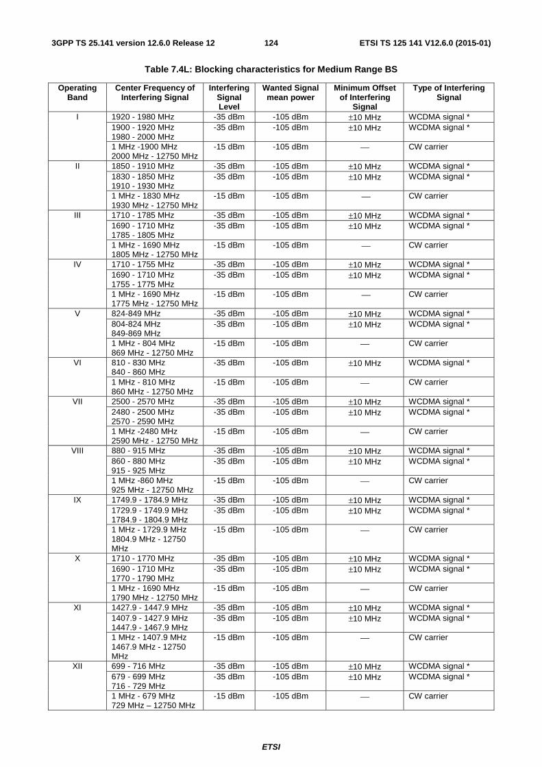
ETSI
ETSI TS 125 141 V12.6.0 (2015-01)1243GPP TS 25.141 version 12.6.0 Release 12
Table 7.4L: Blocking characteristics for Medium Range BS
Operating Band
Center Frequency of Interfering Signal
Interfering Signal Level
Wanted Signal mean power
Minimum Offset of Interfering
Signal
Type of Interfering Signal
I 1920 - 1980 MHz -35 dBm -105 dBm ±10 MHz WCDMA signal * 1900 - 1920 MHz 1980 - 2000 MHz
-35 dBm -105 dBm ±10 MHz WCDMA signal *
1 MHz -1900 MHz 2000 MHz - 12750 MHz
-15 dBm -105 dBm ⎯ CW carrier
II 1850 - 1910 MHz -35 dBm -105 dBm ±10 MHz WCDMA signal * 1830 - 1850 MHz 1910 - 1930 MHz
-35 dBm -105 dBm ±10 MHz WCDMA signal *
1 MHz - 1830 MHz 1930 MHz - 12750 MHz
-15 dBm -105 dBm ⎯ CW carrier
III 1710 - 1785 MHz -35 dBm -105 dBm ±10 MHz WCDMA signal * 1690 - 1710 MHz 1785 - 1805 MHz
-35 dBm -105 dBm ±10 MHz WCDMA signal *
1 MHz - 1690 MHz 1805 MHz - 12750 MHz
-15 dBm -105 dBm ⎯ CW carrier
IV 1710 - 1755 MHz -35 dBm -105 dBm ±10 MHz WCDMA signal * 1690 - 1710 MHz 1755 - 1775 MHz
-35 dBm -105 dBm ±10 MHz WCDMA signal *
1 MHz - 1690 MHz 1775 MHz - 12750 MHz
-15 dBm -105 dBm ⎯ CW carrier
V 824-849 MHz -35 dBm -105 dBm ±10 MHz WCDMA signal * 804-824 MHz 849-869 MHz
-35 dBm -105 dBm ±10 MHz WCDMA signal *
1 MHz - 804 MHz 869 MHz - 12750 MHz
-15 dBm -105 dBm ⎯ CW carrier
VI 810 - 830 MHz 840 - 860 MHz
-35 dBm -105 dBm ±10 MHz WCDMA signal *
1 MHz - 810 MHz 860 MHz - 12750 MHz
-15 dBm -105 dBm ⎯ CW carrier
VII 2500 - 2570 MHz -35 dBm -105 dBm ±10 MHz WCDMA signal * 2480 - 2500 MHz 2570 - 2590 MHz
-35 dBm -105 dBm ±10 MHz WCDMA signal *
1 MHz -2480 MHz 2590 MHz - 12750 MHz
-15 dBm -105 dBm ⎯ CW carrier
VIII 880 - 915 MHz -35 dBm -105 dBm ±10 MHz WCDMA signal * 860 - 880 MHz 915 - 925 MHz
-35 dBm -105 dBm ±10 MHz WCDMA signal *
1 MHz -860 MHz 925 MHz - 12750 MHz
-15 dBm -105 dBm ⎯ CW carrier
IX 1749.9 - 1784.9 MHz -35 dBm -105 dBm ±10 MHz WCDMA signal * 1729.9 - 1749.9 MHz 1784.9 - 1804.9 MHz
-35 dBm -105 dBm ±10 MHz WCDMA signal *
1 MHz - 1729.9 MHz 1804.9 MHz - 12750 MHz
-15 dBm -105 dBm ⎯ CW carrier
X 1710 - 1770 MHz -35 dBm -105 dBm ±10 MHz WCDMA signal * 1690 - 1710 MHz 1770 - 1790 MHz
-35 dBm -105 dBm ±10 MHz WCDMA signal *
1 MHz - 1690 MHz 1790 MHz - 12750 MHz
-15 dBm -105 dBm ⎯ CW carrier
XI 1427.9 - 1447.9 MHz -35 dBm -105 dBm ±10 MHz WCDMA signal * 1407.9 - 1427.9 MHz 1447.9 - 1467.9 MHz
-35 dBm -105 dBm ±10 MHz WCDMA signal *
1 MHz - 1407.9 MHz 1467.9 MHz - 12750 MHz
-15 dBm -105 dBm ⎯ CW carrier
XII 699 - 716 MHz -35 dBm -105 dBm ±10 MHz WCDMA signal * 679 - 699 MHz 716 - 729 MHz
-35 dBm -105 dBm ±10 MHz WCDMA signal *
1 MHz - 679 MHz 729 MHz – 12750 MHz
-15 dBm -105 dBm ⎯ CW carrier

ETSI
ETSI TS 125 141 V12.6.0 (2015-01)1253GPP TS 25.141 version 12.6.0 Release 12
XIII 777 - 787 MHz -35 dBm -105 dBm ±10 MHz WCDMA signal * 757 - 777 MHz 787 - 807 MHz
-35 dBm -105 dBm ±10 MHz WCDMA signal *
1 - 757 MHz 807 MHz - 12750 MHz
-15 dBm -105 dBm ⎯ CW carrier
XIV 788 - 798 MHz -35 dBm -105 dBm ±10 MHz WCDMA signal * 768 - 788 MHz 798 - 818 MHz
-35 dBm -105 dBm ±10 MHz WCDMA signal *
1 - 768 MHz 818 MHz - 12750 MHz
-15 dBm -105 dBm ⎯ CW carrier
XIX 830 - 845 MHz -35 dBm -105 dBm ±10 MHz WCDMA signal * 810 - 830 MHz 845 - 865 MHz
-35 dBm -105 dBm ±10 MHz WCDMA signal *
1 MHz - 810 MHz 865 MHz - 12750 MHz
-15 dBm -105 dBm ⎯ CW carrier
XX 832 - 862 MHz -35 dBm -105 dBm ±10 MHz WCDMA signal * 821 - 832 MHz 862 - 882 MHz
-35 dBm -105 dBm ±10 MHz WCDMA signal *
1 MHz - 821 MHz 882 MHz - 12750 MHz
-15 dBm -105 dBm ⎯ CW carrier
XXI 1447.9 - 1462.9 MHz -35 dBm -105 dBm ±10 MHz WCDMA signal * 1427.9 - 1447.9 MHz 1462.9 - 1482.9 MHz
-35 dBm -105 dBm ±10 MHz WCDMA signal *
1 MHz - 1427.9 MHz 1482.9 MHz - 12750 MHz
-15 dBm -105 dBm ⎯ CW carrier
XXII 3410 - 3490 MHz -35 dBm -105 dBm ±10 MHz WCDMA signal * 3390 - 3410 MHz 3490 - 3510 MHz
-35 dBm -105 dBm ±10 MHz WCDMA signal *
1 MHz - 3390 MHz 3510 MHz - 12750 MHz
-15 dBm -105 dBm ⎯ CW carrier
XXV 1850 - 1915 MHz -35 dBm -105 dBm ±10 MHz WCDMA signal * 1830 - 1850 MHz 1915 - 1930 MHz
-35 dBm -105 dBm ±10 MHz WCDMA signal *
1 MHz - 1830 MHz 1930 MHz - 12750 MHz
-15 dBm -105 dBm ⎯ CW carrier
XXVI 814-849 MHz -35 dBm -105 dBm ±10 MHz WCDMA signal *
794-814 MHz 849-859 MHz
-35 dBm -105 dBm ±10 MHz WCDMA signal *
1 MHz - 794 MHz 859 MHz - 12750 MHz
-15 dBm -105 dBm ⎯ CW carrier
Note *: The characteristics of the W-CDMA interference signal are specified in Annex I. NOTE**: For a BS capable of multiband operation, in case of interfering signal that is not in the in-band blocking
frequency range of the operating band where the wanted signal is present, the wanted Signal mean power is equal to -109.6 dBm.
NOTE: Table 7.4L assumes that two operating bands, where the downlink frequencies (see Table 3.0) of one band would be within the in-band blocking region of the other band, are not deployed in the same geographical area.
Table 7.4M: Blocking characteristics for Local Area / Home BS
Operating Band
Center Frequency of Interfering Signal
Interfering Signal Level
Wanted Signal mean power
Minimum Offset of Interfering
Signal
Type of Interfering Signal
I 1920 - 1980 MHz -30 dBm -101 dBm ±10 MHz WCDMA signal * 1900 - 1920 MHz 1980 - 2000 MHz
-30 dBm -101 dBm ±10 MHz WCDMA signal *
1 MHz -1900 MHz 2000 MHz - 12750 MHz
-15 dBm -101 dBm ⎯ CW carrier

ETSI
ETSI TS 125 141 V12.6.0 (2015-01)1263GPP TS 25.141 version 12.6.0 Release 12
II 1850 - 1910 MHz -30 dBm -101 dBm ±10 MHz WCDMA signal * 1830 - 1850 MHz 1910 - 1930 MHz
-30 dBm -101 dBm ±10 MHz WCDMA signal *
1 MHz - 1830 MHz 1930 MHz - 12750 MHz
-15 dBm -101 dBm ⎯ CW carrier
III 1710 - 1785 MHz -30 dBm -101 dBm ±10 MHz WCDMA signal * 1690 - 1710 MHz 1785 - 1805 MHz
-30 dBm -101 dBm ±10 MHz WCDMA signal *
1 MHz - 1690 MHz 1805 MHz - 12750 MHz
-15 dBm -101 dBm ⎯ CW carrier
IV 1710 - 1755 MHz -30 dBm -101 dBm ±10 MHz WCDMA signal * 1690 - 1710 MHz 1755 - 1775 MHz
-30 dBm -101 dBm ±10 MHz WCDMA signal *
1 MHz - 1690 MHz 1775 MHz - 12750 MHz
-15 dBm -101 dBm ⎯ CW carrier
V 824-849 MHz -30 dBm -101 dBm ±10 MHz WCDMA signal * 804-824 MHz 849-869 MHz
-30 dBm -101 dBm ±10 MHz WCDMA signal *
1 MHz - 804 MHz 869 MHz - 12750 MHz
-15 dBm -101 dBm ⎯ CW carrier
VI 810 - 830 MHz 840 - 860 MHz
-30 dBm -101 dBm ±10 MHz WCDMA signal *
1 MHz - 810 MHz 860 MHz - 12750 MHz
-15 dBm -101 dBm ⎯ CW carrier
VII 2500 - 2570 MHz -30 dBm -101 dBm ±10 MHz WCDMA signal * 2480 - 2500 MHz 2570 - 2590 MHz
-30 dBm -101 dBm ±10 MHz WCDMA signal *
1 MHz -2480 MHz 2590 MHz - 12750 MHz
-15 dBm -101 dBm ⎯ CW carrier
VIII 880 - 915 MHz -30 dBm -101 dBm ±10 MHz WCDMA signal * 860 - 880 MHz 915 - 925 MHz
-30 dBm -101 dBm ±10 MHz WCDMA signal *
1 MHz -860 MHz 925 MHz - 12750 MHz
-15 dBm -101 dBm ⎯ CW carrier
IX 1749.9 - 1784.9 MHz -30 dBm -101 dBm ±10 MHz WCDMA signal * 1729.9 - 1749.9 MHz 1784.9 - 1804.9 MHz
-30 dBm -101 dBm ±10 MHz WCDMA signal *
1 MHz - 1729.9 MHz 1804.9 MHz - 12750 MHz
-15 dBm -101 dBm ⎯ CW carrier
X 1710 - 1770 MHz -30 dBm -101 dBm ±10 MHz WCDMA signal * 1690 - 1710 MHz 1770 - 1790 MHz
-30 dBm -101 dBm ±10 MHz WCDMA signal *
1 MHz - 1690 MHz 1790 MHz - 12750 MHz
-15 dBm -101 dBm ⎯ CW carrier
XI 1427.9 - 1447.9 MHz -30 dBm -101 dBm ±10 MHz WCDMA signal * 1407.9 - 1427.9 MHz 1447.9 - 1467.9 MHz
-30 dBm -101 dBm ±10 MHz WCDMA signal *
1 MHz - 1407.9 MHz 1467.9 MHz - 12750 MHz
-15 dBm -101 dBm ⎯ CW carrier
XII 699 - 716 MHz -30 dBm -101 dBm ±10 MHz WCDMA signal * 679 - 699 MHz 716 - 729 MHz
-30 dBm -101 dBm ±10 MHz WCDMA signal *
1 MHz - 679 MHz 729 MHz – 12750 MHz
-15 dBm -101 dBm ⎯ CW carrier
XIII 777 - 787 MHz -30 dBm -101 dBm ±10 MHz WCDMA signal * 757 - 777 MHz 787 - 807 MHz
-30 dBm -101 dBm ±10 MHz WCDMA signal *
1 - 757 MHz 807 MHz - 12750 MHz
-15 dBm -101 dBm ⎯ CW carrier
XIV 788 - 798 MHz -30 dBm -101 dBm ±10 MHz WCDMA signal * 768 - 788 MHz 798 - 818 MHz
-30 dBm -101 dBm ±10 MHz WCDMA signal *
1 - 768 MHz 818 MHz - 12750 MHz
-15 dBm -101 dBm ⎯ CW carrier

ETSI
ETSI TS 125 141 V12.6.0 (2015-01)1273GPP TS 25.141 version 12.6.0 Release 12
XIX 830 - 845 MHz -30 dBm -101 dBm ±10 MHz WCDMA signal * 810 - 830 MHz 845 - 865 MHz
-30 dBm -101 dBm ±10 MHz WCDMA signal *
1 MHz - 810 MHz 865 MHz - 12750 MHz
-15 dBm -101 dBm ⎯ CW carrier
XX 832 - 862 MHz -30 dBm -101 dBm ±10 MHz WCDMA signal * 821 - 832 MHz 862 - 882 MHz
-30 dBm -101 dBm ±10 MHz WCDMA signal *
1 MHz - 821 MHz 882 MHz - 12750 MHz
-15 dBm -101 dBm ⎯ CW carrier
XXI 1447.9 - 1462.9 MHz -30 dBm -101 dBm ±10 MHz WCDMA signal *
1427.9 - 1447.9 MHz 1462.9 - 1482.9 MHz
-30 dBm -101 dBm ±10 MHz WCDMA signal *
1 MHz - 1427.9 MHz 1482.9 MHz - 12750 MHz
-15 dBm -101 dBm ⎯ CW carrier
XXII 3410 - 3490 MHz -30 dBm -101 dBm ±10 MHz WCDMA signal *
3390 - 3410 MHz 3490 - 3510 MHz
-30 dBm -101 dBm ±10 MHz WCDMA signal *
1 MHz - 3390 MHz 3510 MHz - 12750 MHz
-15 dBm -101 dBm ⎯ CW carrier
XXV 1850 - 1915 MHz -30 dBm -101 dBm ±10 MHz WCDMA signal *
1830 - 1850 MHz 1915 - 1930 MHz
-30 dBm -101 dBm ±10 MHz WCDMA signal *
1 MHz - 1830 MHz 1930 MHz - 12750 MHz
-15 dBm -101 dBm ⎯ CW carrier
XXVI 814-849 MHz -30 dBm -101 dBm ±10 MHz WCDMA signal *
794-814 MHz 849-859 MHz
-30 dBm -101 dBm ±10 MHz WCDMA signal *
1 MHz - 794 MHz 859 MHz - 12750 MHz
-15 dBm -101 dBm ⎯ CW carrier
Note *: The characteristics of the W-CDMA interference signal are specified in Annex I. NOTE**: For a BS capable of multiband operation, in case of interfering signal that is not in the in-band blocking
frequency range of the operating band where the wanted signal is present, the wanted Signal mean power is equal to -105.6 dBm.
NOTE: Table 7.4M assumes that two operating bands, where the downlink frequencies (see Table 3.0) of one band would be within the in-band blocking region of the other band, are not deployed in the same geographical area.

ETSI
ETSI TS 125 141 V12.6.0 (2015-01)1283GPP TS 25.141 version 12.6.0 Release 12
Table 7.4N: Blocking performance requirement for Wide Area BS when co-located with BS in other bands.
Co-located BS type Center Frequency of Interfering Signal
Interfering Signal mean
power
Wanted Signal mean
power
Type of Interfering
Signal Macro GSM900 921 - 960 MHz +16 dBm -115 dBm CW carrier Macro DCS1800 1805 - 1880 MHz +16 dBm -115 dBm CW carrier Macro PCS1900 1930 - 1990 MHz +16 dBm -115 dBm CW carrier Macro GSM850 or CDMA850
869 - 894 MHz +16 dBm -115 dBm CW carrier
WA UTRA-FDD Band I or E-UTRA Band 1
2110 - 2170 MHz +16 dBm -115 dBm CW carrier
WA UTRA-FDD Band II or E-UTRA Band 2
1930 - 1990 MHz +16 dBm -115 dBm CW carrier
WA UTRA-FDD Band III or E-UTRA Band 3
1805 - 1880 MHz +16 dBm -115 dBm CW carrier
WA UTRA-FDD Band IV or E-UTRA Band 4
2110 - 2155 MHz +16 dBm -115 dBm CW carrier
WA UTRA-FDD Band V or E-UTRA Band 5
869 - 894 MHz +16 dBm -115 dBm CW carrier
WA UTRA-FDD Band VI or E-UTRA Band 6
875 - 885 MHz +16 dBm -115 dBm CW carrier
WA UTRA-FDD Band VII or E-UTRA Band 7
2620 - 2690 MHz +16 dBm -115 dBm CW carrier
WA UTRA-FDD Band VIII or E-UTRA Band 8
925 - 960 MHz +16 dBm -115 dBm CW carrier
WA UTRA-FDD Band IX or E-UTRA Band 9
1844.9 - 1879.9 MHz +16 dBm -115 dBm CW carrier
WA UTRA-FDD Band X or E-UTRA Band 10
2110 - 2170 MHz +16 dBm -115 dBm CW carrier
WA UTRA-FDD Band XI or E-UTRA Band 11
1475.9 - 1495.9 MHz +16 dBm -115 dBm CW carrier
WA UTRA-FDD Band XII or E-UTRA Band 12
729 - 746 MHz +16 dBm -115 dBm CW carrier
WA UTRA-FDD Band XIII or E-UTRA Band 13
746 - 756 MHz +16 dBm -115 dBm CW carrier
WA UTRA-FDD Band XIV or E-UTRA Band 14
758 - 768 MHz +16 dBm -115 dBm CW carrier
WA E-UTRA Band 17 734 - 746 MHz +16 dBm -115 dBm CW carrier WA E-UTRA Band 18 860 – 875 MHz +16 dBm -115 dBm CW carrier WA UTRA-FDD Band XIX or E-UTRA Band 19
875 - 890 MHz +16 dBm -115 dBm CW carrier
WA UTRA-FDD Band XX or E-UTRA Band 20
791 - 821 MHz +16 dBm -115 dBm CW carrier
WA UTRA-FDD Band XXI or E-UTRA Band 21
1495.9 - 1510.9 MHz +16 dBm -115 dBm CW carrier
WA UTRA-FDD Band XXII or E-UTRA Band 22
3510 - 3590 MHz +16 dBm -115 dBm CW carrier
WA E-UTRA Band 23 2180 - 2200 MHz +16 dBm -115 dBm CW carrier WA E-UTRA Band 24 1525 – 1559 MHz +16 dBm -115 dBm CW carrier WA UTRA-FDD Band XXV or E-UTRA Band 25
1930 - 1995 MHz +16 dBm -115 dBm CW carrier
WA UTRA-FDD Band XXVI or E-UTRA Band 26
859 - 894 MHz +16 dBm -115 dBm CW carrier
WA E-UTRA Band 27 852 – 859 MHz +16 dBm -115 dBm CW carrier WA E-UTRA Band 28 758 – 803 MHz +16 dBm -115 dBm CW carrier WA E-UTRA Band 29 717 - 728 MHz +16 dBm -115 dBm CW carrier WA E-UTRA Band 30 2350 – 2360 MHz +16 dBm -115 dBm CW carrier WA E-UTRA Band 31 462.5 – 467.5 MHz +16 dBm -115 dBm CW carrier WA UTRA-FDD Band XXXII or E-UTRA Band 32
1452 – 1496 MHz (NOTE 3)
+ 16 dBm -115 dBm CW carrier
WA UTRA TDD Band a) or E-UTRA Band 33
1900 - 1920 MHz +16 dBm -115 dBm CW carrier
WA UTRA TDD Band a) or E-UTRA Band 34
2010 - 2025 MHz +16 dBm -115 dBm CW carrier
WA UTRA TDD Band d) or 2570 - 2620 MHz +16 dBm -115 dBm CW carrier

ETSI
ETSI TS 125 141 V12.6.0 (2015-01)1293GPP TS 25.141 version 12.6.0 Release 12
E-UTRA Band 38 WA UTRA TDD Band f) or E-UTRA Band 39
1880 - 1920 MHz +16 dBm -115 dBm CW carrie
WA UTRA TDD Band e) E-UTRA Band 40
2300 - 2400 MHz +16 dBm -115 dBm CW carrie
WA E-UTRA Band 41 2496 - 2690 MHz +16 dBm -115 dBm CW carrie WA E-UTRA Band 42 3400 - 3600 MHz +16 dBm -115 dBm CW carrier WA E-UTRA Band 43 3600 - 3800 MHz +16 dBm -115 dBm CW carrier WA E-UTRA Band 44 703 - 803 MHz +16 dBm -115 dBm CW carrier NOTE 1: Except for a BS operating in Band XIII, these requirements do not apply when the interfering
signal falls within any of the supported uplink operating band or in the 10 MHz immediately outside any of th supported e uplink operating band. For a BS operating in band XIII the requirements do not apply when the interfering signal falls within the frequency range 768-797 MHz.
NOTE 2: Some combinations of bands may not be possible to co-site based on the requirements above. The current state-of-the-art technology does not allow a single generic solution for co-location of UTRA FDD with UTRA TDD or E-UTRA TDD on adjacent frequencies for 30dB BS-BS minimum coupling loss. However, there are certain site-engineering solutions that can be used. These techniques are addressed in TR 25.942 [4].
NOTE 3: For a BS operating in band XI or XXI, this requirement applies for interfering signal within the frequency range 1475.9-1495.9 MHz.

ETSI
ETSI TS 125 141 V12.6.0 (2015-01)1303GPP TS 25.141 version 12.6.0 Release 12
Table 7.4P: Blocking performance requirement for Medium Range BS when co-located with BS in other bands.
Co-located BS type Center Frequency of Interfering Signal
Interfering Signal
mean power
Wanted Signal mean
power
Type of Interfering
Signal Micro GSM900 921 - 960 MHz -3 dBm -105 dBm CW carrier Micro DCS1800 1805 - 1880 MHz +5 dBm -105 dBm CW carrier Micro PCS1900 1930 - 1990 MHz +5 dBm -105 dBm CW carrier Micro GSM850 869 - 894 MHz -3 dBm -105 dBm CW carrier
MR UTRA-FDD Band I or E-UTRA Band 1
2110 - 2170 MHz +8 dBm -105 dBm CW carrier
MR UTRA-FDD Band II or E-UTRA Band 2
1930 - 1990 MHz +8 dBm -105 dBm CW carrier
MR UTRA-FDD Band III or E-UTRA Band 3
1805 - 1880 MHz +8 dBm -105 dBm CW carrier
MR UTRA-FDD Band IV or E-UTRA Band 4
2110 - 2155 MHz +8 dBm -105 dBm CW carrier
MR UTRA-FDD Band V or E-UTRA Band 5
869 - 894 MHz +8 dBm -105 dBm CW carrier
MR UTRA-FDD Band VI or E-UTRA Band 6
875 - 885 MHz +8 dBm -105 dBm CW carrier
MR UTRA-FDD Band VII or E-UTRA Band 7
2620 - 2690 MHz +8 dBm -105 dBm CW carrier
MR UTRA-FDD Band VIII or E-UTRA Band 8
925 - 960 MHz +8 dBm -105 dBm CW carrier
MR UTRA-FDD Band IX or E-UTRA Band 9
1844.9 - 1879.9 MHz +8 dBm -105 dBm CW carrier
MR UTRA-FDD Band X or E-UTRA Band 10
2110 - 2170 MHz +8 dBm -105 dBm CW carrier
MR UTRA-FDD Band XI or E-UTRA Band 11
1475.9 - 1495.9 MHz +8 dBm -105 dBm CW carrier
MR UTRA-FDD Band XII or E-UTRA Band 12
729 - 746 MHz +8 dBm -105 dBm CW carrier
MR UTRA-FDD Band XIII or E-UTRA Band 13
746 - 756 MHz +8 dBm -105 dBm CW carrier
MR UTRA-FDD Band XIV or E-UTRA Band 14
758 - 768 MHz +8 dBm -105 dBm CW carrier
MR E-UTRA Band 17 734 - 746 MHz +8 dBm -105 dBm CW carrier MR E-UTRA Band 18 860 – 875 MHz +8 dBm -105 dBm CW carrier
MR UTRA-FDD Band XIX or E-UTRA Band 19
875 - 890 MHz +8 dBm -105 dBm CW carrier
MR UTRA-FDD Band XX or E-UTRA Band 20
791 - 821 MHz +8 dBm -105 dBm CW carrier
MR UTRA-FDD Band XXI or E-UTRA Band 21
1495.9 - 1510.9 MHz +8 dBm -105 dBm CW carrier
MR UTRA-FDD Band XXII or E-UTRA Band 22
3510 - 3590 MHz +8 dBm -105 dBm CW carrier
MR E-UTRA Band 23 2180 - 2200 MHz +8 dBm -105 dBm CW carrier MR E-UTRA Band 24 1525 – 1559 MHz +8 dBm -105 dBm CW carrier MR UTRA-FDD Band
XXV or E-UTRA Band 25 1930 - 1995 MHz +8 dBm -105 dBm CW carrier
MR UTRA-FDD Band XXVI or E-UTRA Band 26
859 - 894 MHz +8 dBm -105 dBm CW carrier
MR E-UTRA Band 27 852 – 859 MHz +8 dBm -105 dBm CW carrier MR E-UTRA Band 28 758 – 803 MHz +8 dBm -105 dBm CW carrier MR E-UTRA Band 29 717 - 728 MHz +8 dBm -105 dBm CW carrier MR E-UTRA Band 30 2350 - 2360 MHz +8 dBm -105 dBm CW carrier MR E-UTRA Band 31 462.5 – 467.5 MHz +8 dBm -105 dBm CW carrier MR UTRA-FDD Band
XXXII or E-UTRA Band 32
1452 – 1496 MHz (NOTE 3)
+8 dBm -105 dBm CW carrier
MR E-UTRA Band 33 1900 - 1920 MHz +8 dBm -105 dBm CW carrier MR E-UTRA Band 34 2010 - 2025 MHz +8 dBm -105 dBm CW carrier MR E-UTRA Band 38 2570 - 2620 MHz +8 dBm -105 dBm CW carrier MR E-UTRA Band 39 1880 - 1920 MHz +8 dBm -105 dBm CW carrier

ETSI
ETSI TS 125 141 V12.6.0 (2015-01)1313GPP TS 25.141 version 12.6.0 Release 12
MR E-UTRA Band 40 2300 - 2400 MHz +8 dBm -105 dBm CW carrier MR E-UTRA Band 41 2496 - 2690 MHz +8 dBm -105 dBm CW carrier MR E-UTRA Band 42 3400 - 3600 MHz +8 dBm -105 dBm CW carrier MR E-UTRA Band 43 3600 - 3800 MHz +8 dBm -105 dBm CW carrier MR E-UTRA Band 44 703 - 803 MHz +8 dBm -105 dBm CW carrier
NOTE 1: Except for a BS operating in Band XIII, these requirements do not apply when the interfering signal falls within any of the supported uplink operating band or in the 10 MHz immediately outside any of the supported uplink operating band. For a BS operating in band XIII the requirements do not apply when the interfering signal falls within the frequency range 768-797 MHz.
NOTE 2: Some combinations of bands may not be possible to co-site based on the requirements above. The current state-of-the-art technology does not allow a single generic solution for co-location of UTRA FDD with UTRA TDD or E-UTRA TDD on adjacent frequencies for 30dB BS-BS minimum coupling loss. However, there are certain site-engineering solutions that can be used. These techniques are addressed in TR 25.942 [4].
NOTE 3: For a BS operating in band XI or XXI, this requirement applies for interfering signal within the frequency range 1475.9-1495.9 MHz.

ETSI
ETSI TS 125 141 V12.6.0 (2015-01)1323GPP TS 25.141 version 12.6.0 Release 12
Table 7.4Q: Blocking performance requirement for Local Area BS when co-located with BS in other bands.
Co-located BS type Center Frequency of Interfering Signal
Interfering Signal
mean power
Wanted Signal mean
power
Type of Interfering
Signal Pico GSM900 921 - 960 MHz -7 dBm -101 dBm CW carrier Pico DCS1800 1805 - 1880 MHz -4 dBm -101 dBm CW carrier Pico PCS1900 1930 - 1990 MHz -4 dBm -101 dBm CW carrier Pico GSM850 869 - 894 MHz -7 dBm -101 dBm CW carrier
LA UTRA-FDD Band I or E-UTRA Band 1
2110 - 2170 MHz -6 dBm -101 dBm CW carrier
LA UTRA-FDD Band II or E-UTRA Band 2
1930 - 1990 MHz -6 dBm -101 dBm CW carrier
LA UTRA-FDD Band III or E-UTRA Band 3
1805 - 1880 MHz -6 dBm -101 dBm CW carrier
LA UTRA-FDD Band IV or E-UTRA Band 4
2110 - 2155 MHz -6 dBm -101 dBm CW carrier
LA UTRA-FDD Band V or E-UTRA Band 5
869 - 894 MHz -6 dBm -101 dBm CW carrier
LA UTRA-FDD Band VI or E-UTRA Band 6
875 - 885 MHz -6 dBm -101 dBm CW carrier
LA UTRA-FDD Band VII or E-UTRA Band 7
2620 - 2690 MHz -6 dBm -101 dBm CW carrier
LA UTRA-FDD Band VIII or E-UTRA Band 8
925 - 960 MHz -6 dBm -101 dBm CW carrier
LA UTRA-FDD Band IX or E-UTRA Band 9
1844.9 - 1879.9 MHz -6 dBm -101 dBm CW carrier
LA UTRA-FDD Band X or E-UTRA Band 10
2110 - 2170 MHz -6 dBm -101 dBm CW carrier
LA UTRA-FDD Band XI or E-UTRA Band 11
1475.9 - 1495.9 MHz -6 dBm -101 dBm CW carrier
LA UTRA-FDD Band XII or E-UTRA Band 12
729 - 746 MHz -6 dBm -101 dBm CW carrier
LA UTRA-FDD Band XIII or E-UTRA Band 13
746 - 756 MHz -6 dBm -101 dBm CW carrier
LA UTRA-FDD Band XIV or E-UTRA Band 14
758 - 768 MHz -6 dBm -101 dBm CW carrier
LA E-UTRA Band 17 734 - 746 MHz -6 dBm -101 dBm CW carrier LA UTRA-FDD Band XIX
or E-UTRA Band 19 875 - 890 MHz -6 dBm -101 dBm CW carrier
LA UTRA-FDD Band XX or E-UTRA Band 20
791 - 821 MHz -6 dBm -101 dBm CW carrier
LA UTRA-FDD Band XXI or E-UTRA Band 21
1495.9 - 1510.9 MHz -6 dBm -101 dBm CW carrier
LA UTRA-FDD Band XXII or E-UTRA Band 22
3510 - 3590 MHz -6 dBm -101 dBm CW carrier
LA E-UTRA Band 23 2180 - 2200 MHz -6 dBm -101 dBm CW carrier LA E-UTRA Band 24 1525 – 1559 MHz -6 dBm -101 dBm CW carrier
LA UTRA-FDD Band XXV or E-UTRA Band 25
1930 - 1995 MHz -6 dBm -101 dBm CW carrier
LA UTRA-FDD Band XXVI or E-UTRA Band 26
859 - 894 MHz -6 dBm -101 dBm CW carrier
LA E-UTRA Band 27 852 - 869 MHz -6 dBm -101 dBm CW carrier LA E-UTRA Band 28 758 – 803 MHz -6 dBm -101 dBm CW carrier LA E-UTRA Band 29 717 - 728 MHz -6 dBm -101 dBm CW carrier LA E-UTRA Band 30 2350 – 2360 MHz -6 dBm -101 dBm CW carrier LA E-UTRA Band 31 462.5 – 467.5 MHz -6 dBm -101 dBm CW carrier LA UTRA_FDD Band
XXXII or E-UTRA Band 32
1452 – 1496 MHz (NOTE 3)
-6 dBm -101 dBm CW carrier
LA UTRA TDD Band a) or E-UTRA Band 33
1900 - 1920 MHz -6 dBm -101 dBm CW carrier
LA UTRA TDD Band a) or E-UTRA Band 34
2010 - 2025 MHz -6 dBm -101 dBm CW carrier
LA UTRA TDD Band d) or E-UTRA Band 38
2570 - 2620 MHz -4 dBm -101 dBm CW carrier

ETSI
ETSI TS 125 141 V12.6.0 (2015-01)1333GPP TS 25.141 version 12.6.0 Release 12
LA UTRA TDD Band f) or E-UTRA Band 39 1880 - 1920 MHz -6 dBm -101 dBm CW carrier
LA UTRA TDD Band e) E-UTRA Band 40 2300 - 2400 MHz -6 dBm -101 dBm CW carrier
LA E-UTRA Band 41 2496 - 2690 MHz -6 dBm -101 dBm CW carrier LA E-UTRA Band 42 3400 - 3600 MHz -6 dBm -101 dBm CW carrier LA E-UTRA Band 43 3600 – 3800 MHz -6 dBm -101 dBm CW carrier LA E-UTRA Band 44 703 – 803 MHz -6 dBm -101 dBm CW carrier
NOTE 1: Except for a BS operating in Band XIII, these requirements do not apply when the interfering signal falls within any of the supported uplink operating band or in the 10 MHz immediately outside any of the supported the uplink operating band. For a BS operating in band XIII the requirements do not apply when the interfering signal falls within the frequency range 768-797 MHz.
NOTE 2: Some combinations of bands may not be possible to co-site based on the requirements above. The current state-of-the-art technology does not allow a single generic solution for co-location of UTRA FDD with UTRA TDD or E-UTRA TDD on adjacent frequencies for 30dB BS-BS minimum coupling loss. However, there are certain site-engineering solutions that can be used. These techniques are addressed in TR 25.942 [4].
NOTE 3: For a BS operating in band XI or XXI, this requirement applies for interfering signal within the frequency range 1475.9-1495.9 MHz.
Table 7.4R: Blocking performance requirement (narrowband) for Wide Area BS
Operating Band
Center Frequency of Interfering Signal
Interfering Signal
mean power
Wanted Signal mean
power
Minimum Offset of Interfering
Signal
Type of Interfering Signal
II 1850 - 1910 MHz - 47 dBm -115 dBm ±2.7 MHz GMSK modulated* III 1710 - 1785 MHz - 47 dBm -115 dBm ±2.8 MHz GMSK modulated* IV 1710 - 1755 MHz - 47 dBm -115 dBm ±2.7 MHz GMSK modulated* V 824 - 849 MHz - 47 dBm -115 dBm ±2.7 MHz GMSK modulated*
VIII 880 - 915 MHz - 47 dBm -115 dBm ±2.8 MHz GMSK modulated* X 1710 - 1770 MHz - 47 dBm -115 dBm ±2.7 MHz GMSK modulated*
XII 699 - 716 MHz - 47 dBm -115 dBm ±2.7 MHz GMSK modulated* XIII 777 - 787 MHz - 47 dBm -115 dBm ±2.7 MHz GMSK modulated* XIV 788 - 798 MHz - 47 dBm -115 dBm ±2.7 MHz GMSK modulated* XXV 1850 - 1915 MHz - 47 dBm -115 dBm ±2.7 MHz GMSK modulated* XXVI 814-849 MHz -47 dBm -115 dBm ±2.7 MHz GMSK modulated*
Note *: GMSK modulation as defined in TS 45.004 [12].
Table 7.4S: Blocking performance requirement (narrowband) for Medium range BS
Operating Band
Center Frequency of Interfering Signal
Interfering Signal mean power
Wanted Signal mean power
Minimum Offset of Interfering
Signal
Type of Interfering Signal
II 1850 - 1910 MHz - 42 dBm -105 dBm ±2.7 MHz GMSK modulated* III 1710 - 1785 MHz - 42 dBm -105 dBm ±2.8 MHz GMSK modulated* IV 1710 - 1755 MHz - 42 dBm -105 dBm ±2.7 MHz GMSK modulated* V 824 - 849 MHz - 42 dBm -105 dBm ±2.7 MHz GMSK modulated*
VIII 880 - 915 MHz - 42 dBm -105 dBm ±2.8 MHz GMSK modulated* X 1710 - 1770 MHz - 42 dBm -105 dBm ±2.7 MHz GMSK modulated*
XII 699 - 716 MHz - 42 dBm -105 dBm ±2.7 MHz GMSK modulated* XIII 777 - 787 MHz - 42 dBm -105 dBm ±2.7 MHz GMSK modulated* XIV 788 - 798 MHz - 42 dBm -105 dBm ±2.7 MHz GMSK modulated* XXV 1850 - 1915 MHz - 42 dBm -105 dBm ±2.7 MHz GMSK modulated* XXVI 814-849 MHz - 42 dBm -105 dBm ±2.7 MHz GMSK modulated*
Note *: GMSK modulation as defined in TS 45.004 [12].

ETSI
ETSI TS 125 141 V12.6.0 (2015-01)1343GPP TS 25.141 version 12.6.0 Release 12
Table 7.4T: Blocking performance requirement (narrowband) for Local Area / Home BS
Operating Band
Center Frequency of Interfering Signal
Interfering Signal mean power
Wanted Signal mean power
Minimum Offset of Interfering
Signal
Type of Interfering Signal
II 1850 - 1910 MHz - 37 dBm -101 dBm ±2.7 MHz GMSK modulated* III 1710 - 1785 MHz - 37 dBm -101 dBm ±2.8 MHz GMSK modulated* IV 1710 - 1755 MHz - 37 dBm -101 dBm ±2.7 MHz GMSK modulated* V 824 - 849 MHz - 37 dBm -101 dBm ±2.7 MHz GMSK modulated*
VIII 880 - 915 MHz - 37 dBm -101 dBm ±2.8 MHz GMSK modulated* X 1710 - 1770 MHz - 37 dBm -101 dBm ±2.7 MHz GMSK modulated*
XII 699 - 716 MHz - 37 dBm -101 dBm ±2.7 MHz GMSK modulated* XIII 777 - 787 MHz - 37 dBm -101 dBm ±2.7 MHz GMSK modulated* XIV 788 - 798 MHz - 37 dBm -101 dBm ±2.7 MHz GMSK modulated* XXV 1850 – 1915 MHz - 37 dBm -101 dBm ±2.7 MHz GMSK modulated* XXVI 814-849 MHz - 37 dBm -101 dBm ±2.7 MHz GMSK modulated*
Note *: GMSK modulation as defined in TS 45.004 [12].
Table 7.4U: Void
Table 7.4V: Void
NOTE 1: If the above Test Requirement differs from the Minimum Requirement then the Test Tolerance applied for this test is non-zero. The Test Tolerance for this test is defined in clause 4.2 and the explanation of how the Minimum Requirement has been relaxed by the Test Tolerance is given in Annex F.
NOTE 2: Annex C describes the procedure for BER tests taking into account the statistical consequence of frequent repetition of BER measurements within the blocking test . The consequence is: a DUT exactly on the limit may fail due to the statistical nature 2.55 times(mean value) in 12750 BER measurements using the predefined wrong decision probability of 0.02%. If the fail cases are ≤12, it is allowed to repeat the fail cases 1 time before the final verdict.
7.6 Intermodulation characteristics
7.6.1 Definition and applicability
Third and higher order mixing of the two interfering RF signals can produce an interfering signal in the band of the desired channel. Intermodulation response rejection is a measure of the capability of the receiver to receive a wanted signal on its assigned channel frequency in the presence of two or more interfering signals which have a specific frequency relationship to the wanted signal.
7.6.2 Minimum Requirement
The minimum requirement is in TS 25.104 [1] clause 7.6.
7.5(a): (void)
Table 7.5(b): (void)
7.6.3 Test purpose
The test purpose is to verify the ability of the BS receiver to inhibit the generation of intermodulation products in its non-linear elements caused by the presence of two high-level interfering signals at frequencies with a specific relationship to the frequency of the wanted signal.
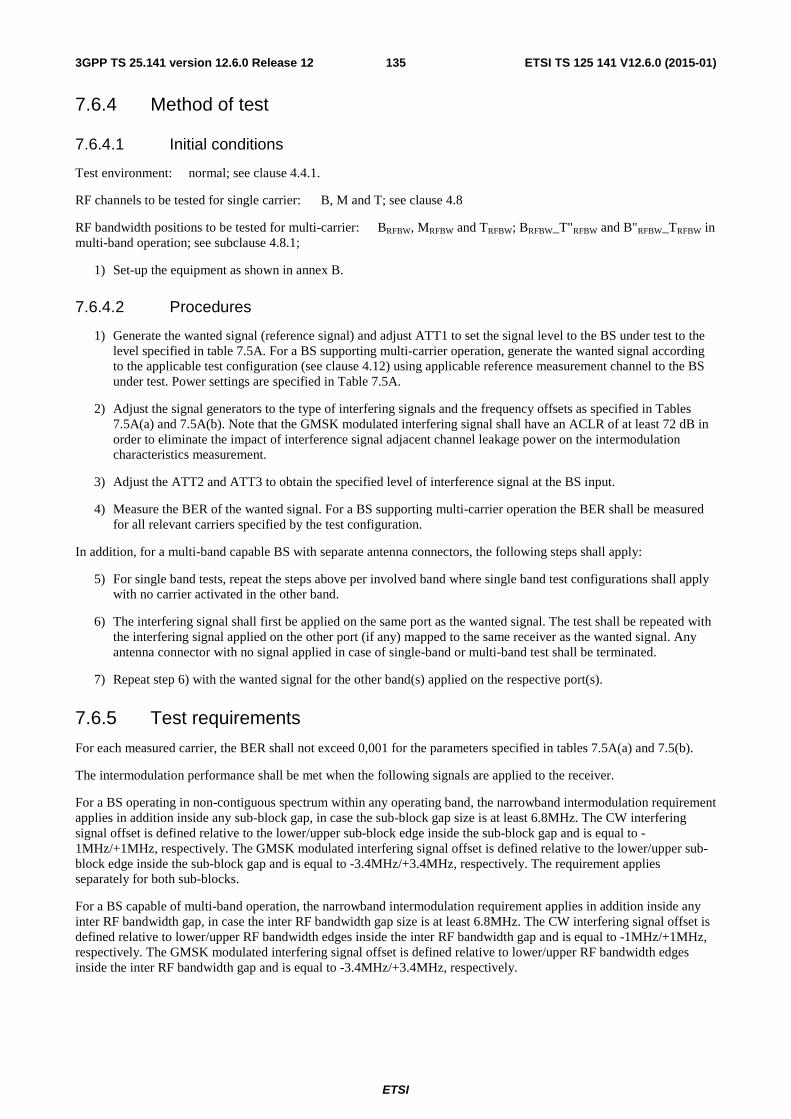
ETSI
ETSI TS 125 141 V12.6.0 (2015-01)1353GPP TS 25.141 version 12.6.0 Release 12
7.6.4 Method of test
7.6.4.1 Initial conditions
Test environment: normal; see clause 4.4.1.
RF channels to be tested for single carrier: B, M and T; see clause 4.8
RF bandwidth positions to be tested for multi-carrier: BRFBW, MRFBW and TRFBW; BRFBW_T"RFBW and B"RFBW_TRFBW in multi-band operation; see subclause 4.8.1;
1) Set-up the equipment as shown in annex B.
7.6.4.2 Procedures
1) Generate the wanted signal (reference signal) and adjust ATT1 to set the signal level to the BS under test to the level specified in table 7.5A. For a BS supporting multi-carrier operation, generate the wanted signal according to the applicable test configuration (see clause 4.12) using applicable reference measurement channel to the BS under test. Power settings are specified in Table 7.5A.
2) Adjust the signal generators to the type of interfering signals and the frequency offsets as specified in Tables 7.5A(a) and 7.5A(b). Note that the GMSK modulated interfering signal shall have an ACLR of at least 72 dB in order to eliminate the impact of interference signal adjacent channel leakage power on the intermodulation characteristics measurement.
3) Adjust the ATT2 and ATT3 to obtain the specified level of interference signal at the BS input.
4) Measure the BER of the wanted signal. For a BS supporting multi-carrier operation the BER shall be measured for all relevant carriers specified by the test configuration.
In addition, for a multi-band capable BS with separate antenna connectors, the following steps shall apply:
5) For single band tests, repeat the steps above per involved band where single band test configurations shall apply with no carrier activated in the other band.
6) The interfering signal shall first be applied on the same port as the wanted signal. The test shall be repeated with the interfering signal applied on the other port (if any) mapped to the same receiver as the wanted signal. Any antenna connector with no signal applied in case of single-band or multi-band test shall be terminated.
7) Repeat step 6) with the wanted signal for the other band(s) applied on the respective port(s).
7.6.5 Test requirements
For each measured carrier, the BER shall not exceed 0,001 for the parameters specified in tables 7.5A(a) and 7.5(b).
The intermodulation performance shall be met when the following signals are applied to the receiver.
For a BS operating in non-contiguous spectrum within any operating band, the narrowband intermodulation requirement applies in addition inside any sub-block gap, in case the sub-block gap size is at least 6.8MHz. The CW interfering signal offset is defined relative to the lower/upper sub-block edge inside the sub-block gap and is equal to -1MHz/+1MHz, respectively. The GMSK modulated interfering signal offset is defined relative to the lower/upper sub-block edge inside the sub-block gap and is equal to -3.4MHz/+3.4MHz, respectively. The requirement applies separately for both sub-blocks.
For a BS capable of multi-band operation, the narrowband intermodulation requirement applies in addition inside any inter RF bandwidth gap, in case the inter RF bandwidth gap size is at least 6.8MHz. The CW interfering signal offset is defined relative to lower/upper RF bandwidth edges inside the inter RF bandwidth gap and is equal to -1MHz/+1MHz, respectively. The GMSK modulated interfering signal offset is defined relative to lower/upper RF bandwidth edges inside the inter RF bandwidth gap and is equal to -3.4MHz/+3.4MHz, respectively.

ETSI
ETSI TS 125 141 V12.6.0 (2015-01)1363GPP TS 25.141 version 12.6.0 Release 12
Table 7.5A(a): Intermodulation performance requirement
Operating Band
Type of Signal Offset Signal mean power Wide Area BS Medium Range BS Local Area / Home
BS All bands Wanted signal - -115 dBm -105 dBm -101 dBm
CW signal ±10 MHz -48 dBm -44 dBm -38 dBm WCDMA signal * ±20 MHz -48 dBm -44 dBm -38 dBm
Note*: The characteristics of the W-CDMA interference signal are specified in Annex I.
Table 7.5A(b): Narrowband intermodulation performance requirement
Operating band
Type of Signal Offset Signal mean power Wide Area BS Medium Range BS Local Area / Home
BS II, III, IV, V, VIII, X, XII, XIII, XIV,
XXV, XXVI
Wanted signal - -115 dBm -105 dBm -101 dBm CW signal ±3.5
MHz - 47 dBm - 43 dBm -37 dBm
GMSK modulated*
±5.9 MHz
- 47 dBm - 43 dBm -37 dBm
Note *: GMSK as defined in TS 45.004 [12].
NOTE: If the above Test Requirement differs from the Minimum Requirement then the Test Tolerance applied for this test is non-zero. The Test Tolerance for this test is defined in clause 4.2 and the explanation of how the Minimum Requirement has been relaxed by the Test Tolerance is given in Annex F.
7.7 Spurious Emissions
7.7.1 Definition and applicability
The spurious emission power is the power of the emissions generated or amplified in a receiver that appears at the BS antenna connector. The requirements apply to all BS with separate RX and TX antenna port. The test shall be performed when both TX and RX are on with the TX port terminated.
For all BS with common RX and TX antenna port the transmitter spurious emission as specified in clause 6.5.3 is valid.
7.7.2 Minimum Requirements
The minimum requirement is in TS 25.104 [1] clause 7.7.
Table 7.6(a): (void)
Table 7.6(b): (void)
7.7.3 Test purpose
The test purpose is to verify the ability of the BS to limit the interference caused by receiver spurious emissions to other systems.
7.7.4 Method of test
7.7.4.1 Initial conditions
Test environment: normal; see clause 4.4.1.
RF channels to be tested for single carrier: M. See clause 4.8
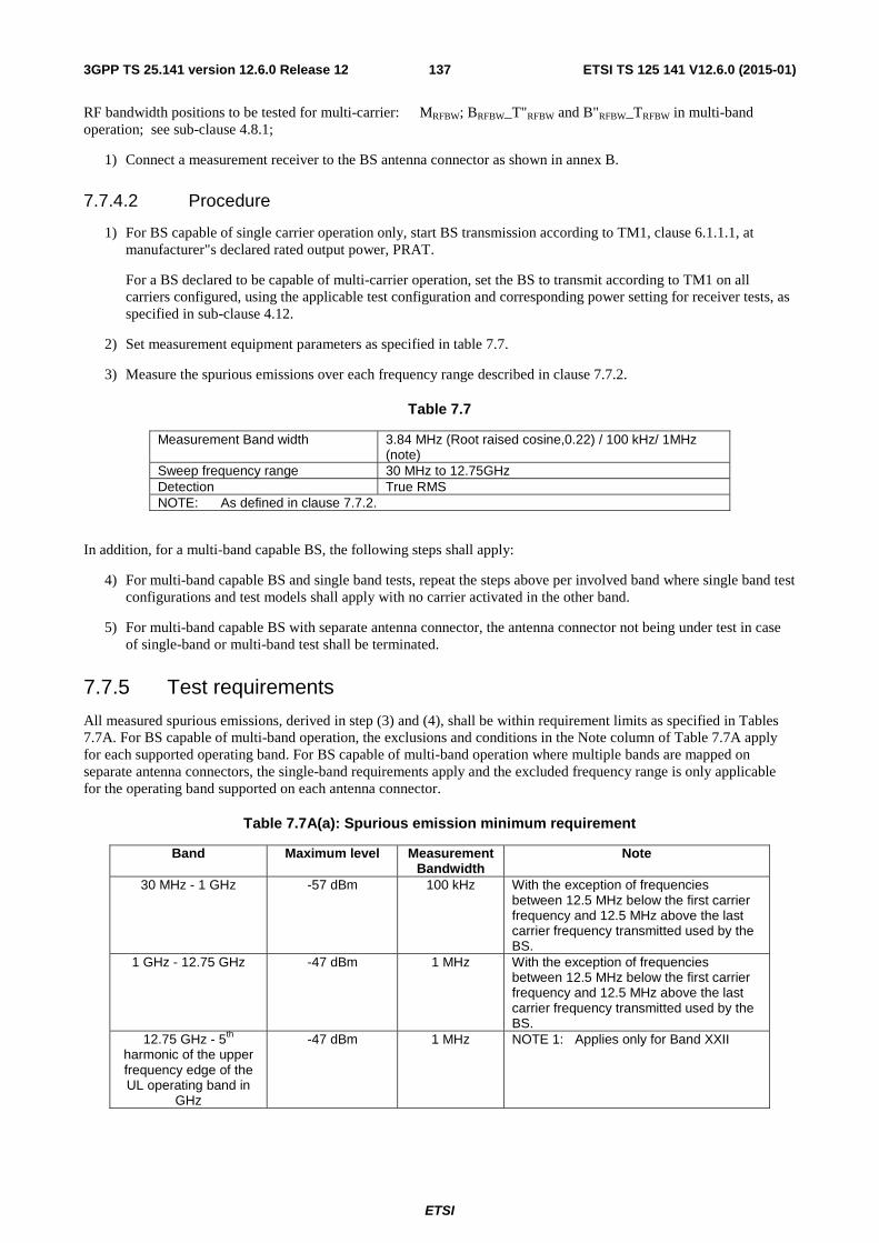
ETSI
ETSI TS 125 141 V12.6.0 (2015-01)1373GPP TS 25.141 version 12.6.0 Release 12
RF bandwidth positions to be tested for multi-carrier: MRFBW; BRFBW_T"RFBW and B"RFBW_TRFBW in multi-band operation; see sub-clause 4.8.1;
1) Connect a measurement receiver to the BS antenna connector as shown in annex B.
7.7.4.2 Procedure
1) For BS capable of single carrier operation only, start BS transmission according to TM1, clause 6.1.1.1, at manufacturer"s declared rated output power, PRAT.
For a BS declared to be capable of multi-carrier operation, set the BS to transmit according to TM1 on all carriers configured, using the applicable test configuration and corresponding power setting for receiver tests, as specified in sub-clause 4.12.
2) Set measurement equipment parameters as specified in table 7.7.
3) Measure the spurious emissions over each frequency range described in clause 7.7.2.
Table 7.7
Measurement Band width 3.84 MHz (Root raised cosine,0.22) / 100 kHz/ 1MHz (note)
Sweep frequency range 30 MHz to 12.75GHz Detection True RMS NOTE: As defined in clause 7.7.2.
In addition, for a multi-band capable BS, the following steps shall apply:
4) For multi-band capable BS and single band tests, repeat the steps above per involved band where single band test configurations and test models shall apply with no carrier activated in the other band.
5) For multi-band capable BS with separate antenna connector, the antenna connector not being under test in case of single-band or multi-band test shall be terminated.
7.7.5 Test requirements
All measured spurious emissions, derived in step (3) and (4), shall be within requirement limits as specified in Tables 7.7A. For BS capable of multi-band operation, the exclusions and conditions in the Note column of Table 7.7A apply for each supported operating band. For BS capable of multi-band operation where multiple bands are mapped on separate antenna connectors, the single-band requirements apply and the excluded frequency range is only applicable for the operating band supported on each antenna connector.
Table 7.7A(a): Spurious emission minimum requirement
Band Maximum level Measurement Bandwidth
Note
30 MHz - 1 GHz -57 dBm 100 kHz With the exception of frequencies between 12.5 MHz below the first carrier frequency and 12.5 MHz above the last carrier frequency transmitted used by the BS.
1 GHz - 12.75 GHz -47 dBm 1 MHz With the exception of frequencies between 12.5 MHz below the first carrier frequency and 12.5 MHz above the last carrier frequency transmitted used by the BS.
12.75 GHz - 5th harmonic of the upper frequency edge of the UL operating band in
GHz
-47 dBm 1 MHz NOTE 1: Applies only for Band XXII

ETSI
ETSI TS 125 141 V12.6.0 (2015-01)1383GPP TS 25.141 version 12.6.0 Release 12
In addition to the requirements in Table 7.7A(a), the power of any spurious emission shall not exceed the levels specified for Protection of the BS receiver of own or different BS in clause 6.5.3.7.3 and for Co-existence with other systems in the same geographical area in clause 6.5.3.7.4 and 6.5.3.7.8.1. In addition, the co-existence requirements for co-located base stations specified in clause 6.5.3.7.5 and 6.5.3.7.8.2 may also be applied.
Table 7.7A(b): Void
Table 7.7A(c): Void
NOTE: If the above Test Requirement differs from the Minimum Requirement then the Test Tolerance applied for this test is non-zero. The Test Tolerance for this test is defined in clause 4.2 and the explanation of how the Minimum Requirement has been relaxed by the Test Tolerance is given in Annex F.
7.8 Verification of the internal BER calculation
7.8.1 Definition and applicability
Base Station System with internal BER calculation can synchronise it's receiver to known pseudo-random data sequence and calculates bit error ratio from the received data. This test is performed only if Base Station System has this kind of feature. This test is performed by feeding measurement signal with known BER to the input of the receiver. Locations of the erroneous bits shall be randomly distributed within a frame. Erroneous bits shall be inserted to the data bit stream as shown in figure 7.1.
BER insertion
CRC attachment
TrBk concatenation/Code block segment.
Channelcoding
Radio frameequalisation
1st interleaving
Radio framesegmentation
Rate matching TrCH multiplexing
Physical channelsegmentation
Physical channelmapping
2nd interleaving
Information data
PhCH
Figure 7.1: BER insertion into the information data
7.8.2 Minimum Requirement
BER indicated by the Base Station System shall be within ±10% of the BER generated by the RF signal source. Measurement shall be performed for the measurement signal specified in table 7.8.
Table 7.8
Transport channel combination Data rate BER DPCH 12,2 kbps 0,01
7.8.3 Test purpose
To verify that the internal BER calculation accuracy shall meet requirements for conformance testing.
7.8.4 Method of test
7.8.4.1 Initial conditions
Test environment: normal; see clause 4.4.1.
RF channels to be tested: B, M and T; see clause 4.8

ETSI
ETSI TS 125 141 V12.6.0 (2015-01)1393GPP TS 25.141 version 12.6.0 Release 12
1) Connect BS RX antenna connector to the RF signal source or UE simulator as shown in annex B.
2) Set correct signal source parameters as specified in table 7.9.
Table 7.9
Parameter Level/status Unit UL signal level Ref.sens +10 dB dBm/3,84 MHz Data sequence PN9 or longer
7.8.4.2 Procedure
1) Measure the BER of received signal from RF signal source or UE simulator to BS antenna connector.
2) BER calculation shall be done at least over 50 000 bits
In addition, for a multi-band capable BS, the following steps shall apply:
3) For multi-band capable BS and single band tests, repeat the steps above per involved band, with no carrier activated in the other band.
4) For multi-band capable BS with separate antenna connector, the antenna connector not being under test shall be terminated.
7.8.5 Test Requirement
BER indicated by the Base Station System shall be within requirement as specified in clause 7.8.2.
8 Performance requirement
8.1 General All Bit Error Ratio (BER) and Block Error ratio (BLER) measurements shall be carried out according to the general rules for statistical testing defined in ITU-T Recommendation O.153 [5] and Annex C.
If external BLER measurement is not used then the internal BLER calculation shall be used instead. When internal BLER calculation is used, the requirements of the verification test according to 8.6 shall be met in advance.
Performance requirements are specified for a number of test environments and multi-path channel classes.
The requirements only apply to those measurement channels that are supported by the base station. The performance requirements for the high speed train conditions which scenarios defined in Annex D.4A are optional. For FRC8 in Annex 9 and Annex 17 the Non E-DPCCH boosting and E-DPCCH boosting requirement only apply for the option supported by the base station.
Unless stated otherwise, performance requirements apply for a single cell only. Performance requirements for a BS supporting DC-HSUPA are defined in terms of single carrier requirements.
For BS with dual receiver antenna diversity, only the BS performance requirements with Rx diversity are to be tested, the required Eb/N0 shall be applied separately at each antenna port.
For BS without receiver antenna diversity, only the BS performance requirements without Rx diversity are to be tested, the required Eb/N0 shall be applied at the BS Rx antenna port.
In tests performed with signal generators a synchronization signal may be provided, from the base station to the signal generator, to enable correct timing of the wanted signal.
For tests in clause 8 the transmitter may be off.

ETSI
ETSI TS 125 141 V12.6.0 (2015-01)1403GPP TS 25.141 version 12.6.0 Release 12
8.2 Demodulation in static propagation conditions
8.2.1 Demodulation of DCH
8.2.1.1 Definition and applicability
The performance requirement of DCH in static propagation conditions is determined by the maximum Block Error Ratio (BLER ) allowed when the receiver input signal is at a specified Eb/N0 limit. The BLER is calculated for each of the measurement channels supported by the base station.
8.2.1.2 Minimum requirement
The minimum requirement is in TS 25.104 [1] clause 8.2.1.1.
Table 8.1: (void)
8.2.1.3 Test purpose
The test shall verify the receiver's ability to receive the test signal under static propagation conditions with a BLER not exceeding a specified limit.
8.2.1.4 Method of test
8.2.1.4.1 Initial conditions
Test environment: normal; see clause 4.4.1.
RF channels to be tested: B, M and T; see clause 4.8
1) For BS with Rx diversity, connect the BS tester generating the wanted signal and AWGN generators to both BS antenna connectors for diversity reception via a combining network as shown in annex B.
2) For BS without Rx diversity, connect the BS tester generating the wanted signal and AWGN generator to the BS antenna connector via a combining network as shown in annex B.
8.2.1.4.2 Procedure
1) Adjust the AWGN generator depending on the BS class under test at the BS input as follows:
Wide Area: -84 dBm/3.84 MHz
Medium Range: -74 dBm/3.84 MHz
Local Area / Home BS: -70 dBm/3.84 MHz2) The characteristics of the wanted signal shall be configured according to the corresponding UL reference measurement channel defined in annex A.
3) Adjust the equipment so that required Eb/N0 specified in table 8.2 is achieved. To achieve the specified Eb/NO, the ratio of the wanted signal level relative to the AWGN signal at the BS input should be adjusted to: 10*Log10(Rb /3.84*106)+Eb/N0 [ dB].
4) For each of the data rates in table 8.2 applicable for the base station, measure the BLER.
8.2.1.5 Test requirements
The BLER measured according to clause 8.2.1.4.2 shall not exceed the BLER limits for the Eb/N0 levels specified in table 8.2.
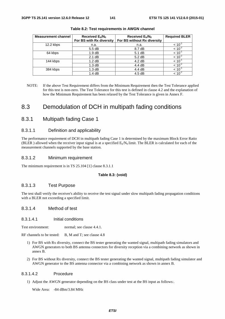
ETSI
ETSI TS 125 141 V12.6.0 (2015-01)1413GPP TS 25.141 version 12.6.0 Release 12
Table 8.2: Test requirements in AWGN channel
Measurement channel Received Eb/N0
For BS with Rx diversity Received Eb/N0
For BS without Rx diversity Required BLER
12.2 kbps n.a. n.a. < 10-1 5.5 dB 8.7 dB < 10-2
64 kbps 1.9 dB 5.1 dB < 10-1 2.1 dB 5.2 dB < 10-2
144 kbps 1.2 dB 4.2 dB < 10-1 1.3 dB 4.4 dB < 10-2
384 kbps 1.3 dB 4.4 dB < 10-1 1.4 dB 4.5 dB < 10-2
NOTE: If the above Test Requirement differs from the Minimum Requirement then the Test Tolerance applied for this test is non-zero. The Test Tolerance for this test is defined in clause 4.2 and the explanation of how the Minimum Requirement has been relaxed by the Test Tolerance is given in Annex F.
8.3 Demodulation of DCH in multipath fading conditions
8.3.1 Multipath fading Case 1
8.3.1.1 Definition and applicability
The performance requirement of DCH in multipath fading Case 1 is determined by the maximum Block Error Ratio (BLER ) allowed when the receiver input signal is at a specified Eb/N0 limit. The BLER is calculated for each of the measurement channels supported by the base station.
8.3.1.2 Minimum requirement
The minimum requirement is in TS 25.104 [1] clause 8.3.1.1
Table 8.3: (void)
8.3.1.3 Test Purpose
The test shall verify the receiver's ability to receive the test signal under slow multipath fading propagation conditions with a BLER not exceeding a specified limit.
8.3.1.4 Method of test
8.3.1.4.1 Initial conditions
Test environment: normal; see clause 4.4.1.
RF channels to be tested: B, M and T; see clause 4.8
1) For BS with Rx diversity, connect the BS tester generating the wanted signal, multipath fading simulators and AWGN generators to both BS antenna connectors for diversity reception via a combining network as shown in annex B.
2) For BS without Rx diversity, connect the BS tester generating the wanted signal, multipath fading simulator and AWGN generator to the BS antenna connector via a combining network as shown in annex B.
8.3.1.4.2 Procedure
1) Adjust the AWGN generator depending on the BS class under test at the BS input as follows:.
Wide Area: -84 dBm/3.84 MHz

ETSI
ETSI TS 125 141 V12.6.0 (2015-01)1423GPP TS 25.141 version 12.6.0 Release 12
Medium Range: -74 dBm/3.84 MHz
Local Area / Home BS: -70 dBm/3.84 MHz
2) The characteristics of the wanted signal shall be configured according to the corresponding UL reference measurement channel defined in annex A.
3) The multipath fading emulators shall be configured according to the corresponding channel model defined in annex D.
4) Adjust the equipment so that required Eb/N0 specified in table 8.4 is achieved. To achieve the specified Eb/NO, the ratio of the wanted signal level relative to the AWGN signal at the BS input should be adjusted to: 10*Log10(Rb /3.84*106)+Eb/N0 [ dB].
5) For each of the data rates in table 8.4 applicable for the base station, measure the BLER.
8.3.1.5 Test requirements
The BLER measured according to clause 8.3.1.4.2 shall not exceed the BLER limits for the Eb/N0 levels specified in table 8.4.
Table 8.4: Test requirements in multipath Case 1 channel
Measurement channel Received Eb/N0
For BS with Rx diversity Received Eb/N0
For BS without Rx diversity Required BLER
12.2 kbps n.a. n.a. < 10-1 12.5 dB 19.7 dB < 10-2
64 kbps 6.8 dB 12.2 dB < 10-1 9.8 dB 16.5 dB < 10-2
144 kbps 6.0 dB 11.4 dB < 10-1 9.0 dB 15.6 dB < 10-2
384 kbps 6.4 dB 11.8 dB < 10-1 9.4 dB 16.1 dB < 10-2
NOTE: If the above Test Requirement differs from the Minimum Requirement then the Test Tolerance applied for this test is non-zero. The Test Tolerance for this test is defined in clause 4.2 and the explanation of how the Minimum Requirement has been relaxed by the Test Tolerance is given in Annex F.
8.3.2 Multipath fading Case 2
8.3.2.1 Definition and applicability
The performance requirement of DCH in multipath fading Case 2 is determined by the maximum Block Error Rate (BLER) allowed when the receiver input signal is at a specified Eb/N0 limit. The BLER is calculated for each of the measurement channels supported by the base station.
The requirement shall not be applied to Home BS.
8.3.2.2 Minimum requirement
The minimum requirement is in TS 25.104 [1] clause 8.3.2.1.
Table 8.5: (void)
8.3.2.3 Test Purpose
The test shall verify the receiver"s ability to receive the test signal that has a large time dispersion with a BLER not exceeding a specified limit.

ETSI
ETSI TS 125 141 V12.6.0 (2015-01)1433GPP TS 25.141 version 12.6.0 Release 12
8.3.2.4 Method of test
8.3.2.4.1 Initial conditions
Test environment: normal; see clause 4.4.1.
RF channels to be tested: B, M and T; see clause 4.8
1) For BS with Rx diversity, connect the BS tester generating the wanted signal, multipath fading simulators and AWGN generators to both BS antenna connectors for diversity reception via a combining network as shown in annex B.
2) For BS without Rx diversity, connect the BS tester generating the wanted signal, multipath fading simulator and AWGN generator to the BS antenna connector via a combining network as shown in annex B.
8.3.2.4.2 Procedure
1) Adjust the AWGN generator depending on the BS class under test at the BS input as follows:.
Wide Area: -84 dBm/3.84 MHz
Medium Range: -74 dBm/3.84 MHz
Local Area: -70 dBm/3.84 MHz
2) The characteristics of the wanted signal shall be configured according to the corresponding UL reference measurement channel defined in annex A.
3) The multipath fading emulators shall be configured according to the corresponding channel model defined in annex D.
4) Adjust the equipment so that required Eb/N0 specified in table 8.6 is achieved. To achieve the specified Eb/NO, the ratio of the wanted signal level relative to the AWGN signal at the BS input should be adjusted to: 10*Log10(Rb /3.84*106)+Eb/N0 [ dB].
5) For each of the data rates in table 8.6 applicable for the base station, measure the BLER.
8.3.2.5 Test requirements
The BLER measured according to clause 8.3.2.4.2 shall not exceed the BLER limits for the Eb/N0 levels specified in table 8.5.
Table 8.6: Test requirements in multipath Case 2 channel
Measurement channel Received Eb/N0
For BS with Rx Diversity Received Eb/N0
For BS without Rx Diversity Required BLER
12.2 kbps n.a. n.a. < 10-1 9.6 dB 15.6 dB < 10-2
64 kbps 4.9 dB 9.8 dB < 10-1 7.0 dB 12.9 dB < 10-2
144 kbps 4.3 dB 8.8 dB < 10-1 6.2 dB 12.1 dB < 10-2
384 kbps 4.7 dB 9.3 dB < 10-1 6.7 dB 12.7 dB < 10-2
NOTE: If the above Test Requirement differs from the Minimum Requirement then the Test Tolerance applied for this test is non-zero. The Test Tolerance for this test is defined in clause 4.2 and the explanation of how the Minimum Requirement has been relaxed by the Test Tolerance is given in Annex F.

ETSI
ETSI TS 125 141 V12.6.0 (2015-01)1443GPP TS 25.141 version 12.6.0 Release 12
8.3.3 Multipath fading Case 3
8.3.3.1 Definition and applicability
The performance requirement of DCH in multipath fading Case 3 is determined by the maximum Block Error Ratio (BLER) allowed when the receiver input signal is at a specified Eb/N0 limit. The BLER is calculated for each of the measurement channels supported by the base station.
The requirement shall not be applied to Home BS.
8.3.3.2 Minimum requirement
The minimum requirement is in TS 25.104 [1] clause 8.3.3.1.
Table 8.7: (void)
8.3.3.3 Test purpose
The test shall verify the receivers ability to receive the test signal under fast fading propagation conditions with a BLER not exceeding a specified limit.
8.3.3.4 Method of test
8.3.3.4.1 Initial conditions
Test environment: normal; see clause 4.4.1.
RF channels to be tested: B, M and T; see clause 4.8
1) For BS with Rx diversity, connect the BS tester generating the wanted signal, multipath fading simulators and AWGN generators to both BS antenna connectors for diversity reception via a combining network as shown in annex B.
2) For BS without Rx diversity, connect the BS tester generating the wanted signal, multipath fading simulator and AWGN generator to the BS antenna connector via a combining network as shown in annex B.
8.3.3.4.2 Procedure
1) Adjust the AWGN generator depending on the BS class under test at the BS input as follows:.
Wide Area: -84 dBm/3.84 MHz
Medium Range: -74 dBm/3.84 MHz
Local Area: -70 dBm/3.84 MHz
2) The characteristics of the wanted signal shall be configured according to the corresponding UL reference measurement channel defined in annex A.
3) The multipath fading emulators shall be configured according to the corresponding channel model defined in annex D.
4) Adjust the equipment so that required Eb/N0 specified in table 8.8 is achieved. To achieve the specified Eb/NO, the ratio of the wanted signal level relative to the AWGN signal at the BS input should be adjusted to: 10*Log10(Rb /3.84*106)+Eb/N0 [ dB].
5) For each of the data rates in table 8.8 applicable for the base station, measure the BLER
8.3.3.5 Test requirements
The BLER measured according to clause 8.3.3.4.2 shall not exceed the BLER limits for Eb/N0 levels specified in table 8.7.
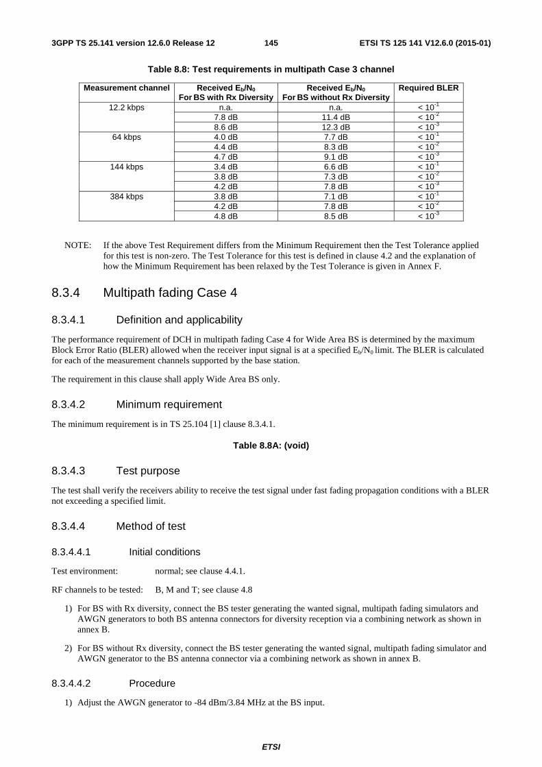
ETSI
ETSI TS 125 141 V12.6.0 (2015-01)1453GPP TS 25.141 version 12.6.0 Release 12
Table 8.8: Test requirements in multipath Case 3 channel
Measurement channel Received Eb/N0
For BS with Rx Diversity Received Eb/N0
For BS without Rx Diversity Required BLER
12.2 kbps n.a. n.a. < 10-1 7.8 dB 11.4 dB < 10-2 8.6 dB 12.3 dB < 10-3
64 kbps 4.0 dB 7.7 dB < 10-1 4.4 dB 8.3 dB < 10-2 4.7 dB 9.1 dB < 10-3
144 kbps 3.4 dB 6.6 dB < 10-1 3.8 dB 7.3 dB < 10-2 4.2 dB 7.8 dB < 10-3
384 kbps 3.8 dB 7.1 dB < 10-1 4.2 dB 7.8 dB < 10-2 4.8 dB 8.5 dB < 10-3
NOTE: If the above Test Requirement differs from the Minimum Requirement then the Test Tolerance applied for this test is non-zero. The Test Tolerance for this test is defined in clause 4.2 and the explanation of how the Minimum Requirement has been relaxed by the Test Tolerance is given in Annex F.
8.3.4 Multipath fading Case 4
8.3.4.1 Definition and applicability
The performance requirement of DCH in multipath fading Case 4 for Wide Area BS is determined by the maximum Block Error Ratio (BLER) allowed when the receiver input signal is at a specified Eb/N0 limit. The BLER is calculated for each of the measurement channels supported by the base station.
The requirement in this clause shall apply Wide Area BS only.
8.3.4.2 Minimum requirement
The minimum requirement is in TS 25.104 [1] clause 8.3.4.1.
Table 8.8A: (void)
8.3.4.3 Test purpose
The test shall verify the receivers ability to receive the test signal under fast fading propagation conditions with a BLER not exceeding a specified limit.
8.3.4.4 Method of test
8.3.4.4.1 Initial conditions
Test environment: normal; see clause 4.4.1.
RF channels to be tested: B, M and T; see clause 4.8
1) For BS with Rx diversity, connect the BS tester generating the wanted signal, multipath fading simulators and AWGN generators to both BS antenna connectors for diversity reception via a combining network as shown in annex B.
2) For BS without Rx diversity, connect the BS tester generating the wanted signal, multipath fading simulator and AWGN generator to the BS antenna connector via a combining network as shown in annex B.
8.3.4.4.2 Procedure
1) Adjust the AWGN generator to -84 dBm/3.84 MHz at the BS input.
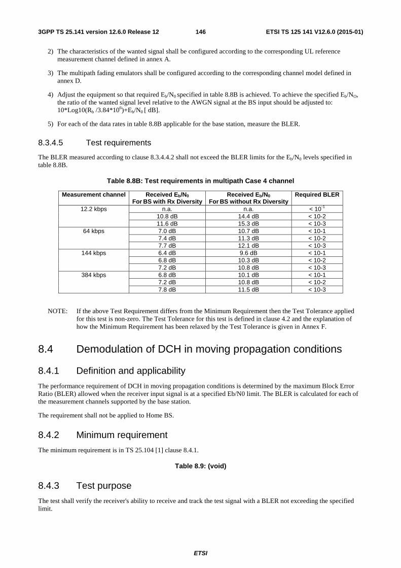
ETSI
ETSI TS 125 141 V12.6.0 (2015-01)1463GPP TS 25.141 version 12.6.0 Release 12
2) The characteristics of the wanted signal shall be configured according to the corresponding UL reference measurement channel defined in annex A.
3) The multipath fading emulators shall be configured according to the corresponding channel model defined in annex D.
4) Adjust the equipment so that required Eb/N0 specified in table 8.8B is achieved. To achieve the specified Eb/NO, the ratio of the wanted signal level relative to the AWGN signal at the BS input should be adjusted to: 10*Log10(Rb /3.84*106)+Eb/N0 [ dB].
5) For each of the data rates in table 8.8B applicable for the base station, measure the BLER.
8.3.4.5 Test requirements
The BLER measured according to clause 8.3.4.4.2 shall not exceed the BLER limits for the Eb/N0 levels specified in table 8.8B.
Table 8.8B: Test requirements in multipath Case 4 channel
Measurement channel Received Eb/N0
For BS with Rx Diversity Received Eb/N0
For BS without Rx Diversity Required BLER
12.2 kbps n.a. n.a. < 10-1 10.8 dB 14.4 dB < 10-2 11.6 dB 15.3 dB < 10-3
64 kbps 7.0 dB 10.7 dB < 10-1 7.4 dB 11.3 dB < 10-2 7.7 dB 12.1 dB < 10-3
144 kbps 6.4 dB 9.6 dB < 10-1 6.8 dB 10.3 dB < 10-2 7.2 dB 10.8 dB < 10-3
384 kbps 6.8 dB 10.1 dB < 10-1 7.2 dB 10.8 dB < 10-2 7.8 dB 11.5 dB < 10-3
NOTE: If the above Test Requirement differs from the Minimum Requirement then the Test Tolerance applied for this test is non-zero. The Test Tolerance for this test is defined in clause 4.2 and the explanation of how the Minimum Requirement has been relaxed by the Test Tolerance is given in Annex F.
8.4 Demodulation of DCH in moving propagation conditions
8.4.1 Definition and applicability
The performance requirement of DCH in moving propagation conditions is determined by the maximum Block Error Ratio (BLER) allowed when the receiver input signal is at a specified Eb/N0 limit. The BLER is calculated for each of the measurement channels supported by the base station.
The requirement shall not be applied to Home BS.
8.4.2 Minimum requirement
The minimum requirement is in TS 25.104 [1] clause 8.4.1.
Table 8.9: (void)
8.4.3 Test purpose
The test shall verify the receiver's ability to receive and track the test signal with a BLER not exceeding the specified limit.
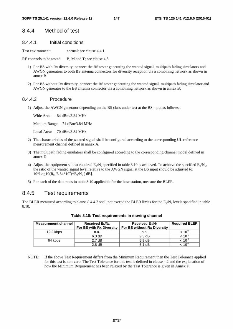
ETSI
ETSI TS 125 141 V12.6.0 (2015-01)1473GPP TS 25.141 version 12.6.0 Release 12
8.4.4 Method of test
8.4.4.1 Initial conditions
Test environment: normal; see clause 4.4.1.
RF channels to be tested: B, M and T; see clause 4.8
1) For BS with Rx diversity, connect the BS tester generating the wanted signal, multipath fading simulators and AWGN generators to both BS antenna connectors for diversity reception via a combining network as shown in annex B.
2) For BS without Rx diversity, connect the BS tester generating the wanted signal, multipath fading simulator and AWGN generator to the BS antenna connector via a combining network as shown in annex B.
8.4.4.2 Procedure
1) Adjust the AWGN generator depending on the BS class under test at the BS input as follows:.
Wide Area: -84 dBm/3.84 MHz
Medium Range: -74 dBm/3.84 MHz
Local Area: -70 dBm/3.84 MHz
2) The characteristics of the wanted signal shall be configured according to the corresponding UL reference measurement channel defined in annex A.
3) The multipath fading emulators shall be configured according to the corresponding channel model defined in annex D.
4) Adjust the equipment so that required Eb/N0 specified in table 8.10 is achieved. To achieve the specified Eb/NO, the ratio of the wanted signal level relative to the AWGN signal at the BS input should be adjusted to: 10*Log10(Rb /3.84*106)+Eb/N0 [ dB].
5) For each of the data rates in table 8.10 applicable for the base station, measure the BLER.
8.4.5 Test requirements
The BLER measured according to clause 8.4.4.2 shall not exceed the BLER limits for the Eb/N0 levels specified in table 8.10.
Table 8.10: Test requirements in moving channel
Measurement channel Received Eb/N0
For BS with Rx Diversity Received Eb/N0
For BS without Rx Diversity Required BLER
12.2 kbps n.a. n.a. < 10-1 6.3 dB 9.3 dB < 10-2
64 kbps 2.7 dB 5.9 dB < 10-1 2.8 dB 6.1 dB < 10-2
NOTE: If the above Test Requirement differs from the Minimum Requirement then the Test Tolerance applied for this test is non-zero. The Test Tolerance for this test is defined in clause 4.2 and the explanation of how the Minimum Requirement has been relaxed by the Test Tolerance is given in Annex F.

ETSI
ETSI TS 125 141 V12.6.0 (2015-01)1483GPP TS 25.141 version 12.6.0 Release 12
8.5 Demodulation of DCH in birth/death propagation conditions
8.5.1 Definition and applicability
The performance requirement of DCH in birth/death propagation conditions is determined by the maximum Block Error Ratio (BLER ) allowed when the receiver input signal is at a specified Eb/N0 limit. The BLER is calculated for each of the measurement channels supported by the base station.
The requirement shall not be applied to Home BS.
8.5.2 Minimum requirement
The minimum requirement is in TS 25.104 [1] clause 8.5.1.
Table 8.11: (void)
8.5.3 Test purpose
The test shall verify the receiver's ability to receive the test signal to find new multi path components with a BLER not exceeding the specified limit.
8.5.4 Method of test
8.5.4.1 Initial conditions
Test environment: normal; see clause 4.4.1.
RF channels to be tested: B, M and T; see clause 4.8
1) For BS with Rx diversity, connect the BS tester generating the wanted signal, multipath fading simulators and AWGN generators to both BS antenna connectors for diversity reception via a combining network as shown in annex B.
2) For BS without Rx diversity, connect the BS tester generating the wanted signal, multipath fading simulator and AWGN generator to the BS antenna connector via a combining network as shown in annex B.
8.5.4.2 Procedure
1) Adjust the AWGN generator depending on the BS class under test at the BS input as follows:.
Wide Area: -84 dBm/3.84 MHz
Medium Range: -74 dBm/3.84 MHz
Local Area: -70 dBm/3.84 MHz
2) The characteristics of the wanted signal shall be configured according to the corresponding UL reference measurement channel defined in annex A.
3) The multipath fading emulators shall be configured according to the corresponding channel model defined in annex D.
4) Adjust the equipment so that required Eb/N0 specified in table 8.12 is achieved. To achieve the specified Eb/NO, the ratio of the wanted signal level relative to the AWGN signal at the BS input should be adjusted to: 10*Log10(Rb /3.84*106)+Eb/N0 [ dB].
5) For each of the data rates in table 8.12 applicable for the base station, measure the BLER.

ETSI
ETSI TS 125 141 V12.6.0 (2015-01)1493GPP TS 25.141 version 12.6.0 Release 12
8.5.5 Test requirements
The BLER measured according to clause 8.5.4.2 shall not exceed the BLER limits for the Eb/N0 levels specified in table 8.12.
Table 8.12: Test requirements in birth/death channel
Measurement channel
Received Eb/N0
For BS with Rx Diversity
Received Eb/N0
For BS without Rx Diversity
Required BLER
12.2 kbps n.a. n.a. < 10-1 8.3 dB 11.4 dB < 10-2
64 kbps 4.7 dB 8.0 dB < 10-1 4.8 dB 8.1 dB < 10-2
NOTE: If the above Test Requirement differs from the Minimum Requirement then the Test Tolerance applied for this test is non-zero. The Test Tolerance for this test is defined in clause 4.2 and the explanation of how the Minimum Requirement has been relaxed by the Test Tolerance is given in Annex F.
8.5A Demodulation of DCH in high speed train conditions
8.5A.1 Definition and applicability
The performance requirement of DCH in high speed train conditions is determined by the maximum Block Error Ratio (BLER) allowed when the receiver input signal is at a specified Eb/N0 limit. The BLER is calculated for 12.2 kbps.
The requirement shall not be applied to Home BS.
8.5A.2 Minimum requirement
The minimum requirement is in TS 25.104 [1] clause 8.5A.2.
8.5A.3 Test purpose
The test shall verify the receiver's ability to receive the test signal in high speed train conditions with a BLER not exceeding the specified limit.
8.5A.4 Method of test
8.5A.4.1 Initial conditions
Test environment: normal; see clause 4.4.1.
RF channels to be tested: B, M and T; see clause 4.8
1) For BS with Rx diversity, connect the BS tester generating the wanted signal, multipath fading simulators and AWGN generators to both BS antenna connectors for diversity reception via a combining network as shown in annex B.
2) For BS without Rx diversity, connect the BS tester generating the wanted signal, multipath fading simulator and AWGN generator to the BS antenna connector via a combining network as shown in annex B.
8.5A.4.2 Procedure
1) Adjust the AWGN generator depending on the BS class under test at the BS input as follows:.
Wide Area: -84 dBm/3.84 MHz
Medium Range: -74 dBm/3.84 MHz
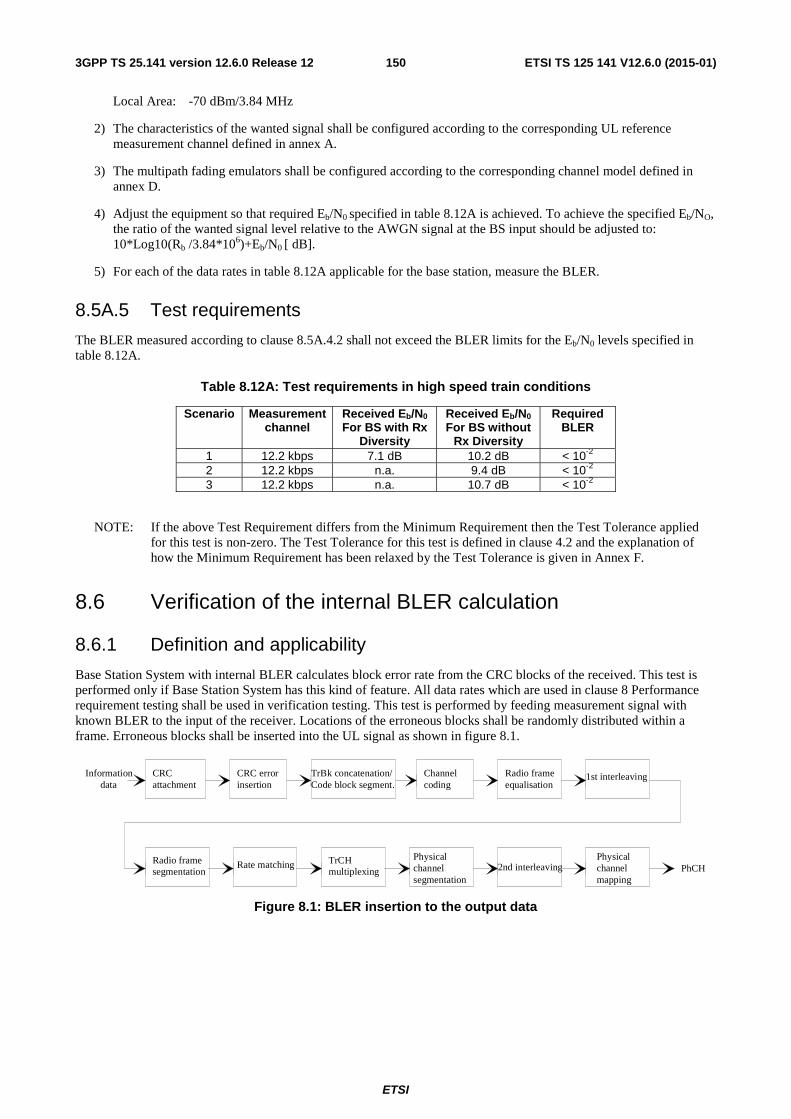
ETSI
ETSI TS 125 141 V12.6.0 (2015-01)1503GPP TS 25.141 version 12.6.0 Release 12
Local Area: -70 dBm/3.84 MHz
2) The characteristics of the wanted signal shall be configured according to the corresponding UL reference measurement channel defined in annex A.
3) The multipath fading emulators shall be configured according to the corresponding channel model defined in annex D.
4) Adjust the equipment so that required Eb/N0 specified in table 8.12A is achieved. To achieve the specified Eb/NO, the ratio of the wanted signal level relative to the AWGN signal at the BS input should be adjusted to: 10*Log10(Rb /3.84*106)+Eb/N0 [ dB].
5) For each of the data rates in table 8.12A applicable for the base station, measure the BLER.
8.5A.5 Test requirements
The BLER measured according to clause 8.5A.4.2 shall not exceed the BLER limits for the Eb/N0 levels specified in table 8.12A.
Table 8.12A: Test requirements in high speed train conditions
Scenario Measurement channel
Received Eb/N0
For BS with Rx Diversity
Received Eb/N0
For BS without Rx Diversity
Required BLER
1 12.2 kbps 7.1 dB 10.2 dB < 10-2 2 12.2 kbps n.a. 9.4 dB < 10-2 3 12.2 kbps n.a. 10.7 dB < 10-2
NOTE: If the above Test Requirement differs from the Minimum Requirement then the Test Tolerance applied for this test is non-zero. The Test Tolerance for this test is defined in clause 4.2 and the explanation of how the Minimum Requirement has been relaxed by the Test Tolerance is given in Annex F.
8.6 Verification of the internal BLER calculation
8.6.1 Definition and applicability
Base Station System with internal BLER calculates block error rate from the CRC blocks of the received. This test is performed only if Base Station System has this kind of feature. All data rates which are used in clause 8 Performance requirement testing shall be used in verification testing. This test is performed by feeding measurement signal with known BLER to the input of the receiver. Locations of the erroneous blocks shall be randomly distributed within a frame. Erroneous blocks shall be inserted into the UL signal as shown in figure 8.1.
CRC error insertion
CRC attachment
TrBk concatenation/Code block segment.
Channelcoding
Radio frameequalisation
1st interleaving
Radio framesegmentation
Rate matching TrCH multiplexing
Physical channelsegmentation
Physical channelmapping
2nd interleaving
Information data
PhCH
Figure 8.1: BLER insertion to the output data

ETSI
ETSI TS 125 141 V12.6.0 (2015-01)1513GPP TS 25.141 version 12.6.0 Release 12
8.6.2 Minimum requirement
BLER indicated by the Base Station System shall be within ±10% of the BLER generated by the RF signal source. Measurement shall be repeated for each data rate as specified in table 8.13.
Table 8.13
Transport channel combination Data rate BLER DPCH 12,2 kbps 0.01 DPCH 64 kbps 0.01 DPCH 144 kbps 0.01 DPCH 384 kbps 0.01
8.6.3 Test purpose
To verify that the internal BLER calculation accuracy shall met requirements for conformance testing.
8.6.4 Method of test
8.6.4.1 Initial conditions
Test environment: normal; see clause 4.4.1.
RF channels to be tested: B, M and T; see clause 4.8
1) For BS with Rx diversity, connect the BS tester generating the wanted signal to both BS antenna connectors for diversity reception via a combining network as shown in annex B.
2) For BS without Rx diversity, connect the BS tester generating the wanted signal to the BS antenna connector as shown in annex B.
3) Set correct signal source parameters depending on the BS class under test as specified in table 8.14.
Table 8.14: UL Signal levels for different data rates
Data rate Signal level for WA BS
Signal level for MR BS
Signal level for LA BS
Unit
12,2 kbps -111 -101 -97 dBm/3.84 MHz 64 kbps -107 -97 -93 dBm/3.84 MHz 144 kbps -104 -94 -90 dBm/3.84 MHz 384 kbps -100 -90 -86 dBm/3.84 MHz
NOTE: PN9 can be used as data sequence for the test
8.6.4.2 Procedure
1) The characteristics of the wanted signal shall be configured according to the corresponding UL reference measurement channel defined in annex A.
2) The BLER insertion to the wanted signal shall be configured according to the corresponding data rate in table 8.13.
3) Adjust the BS tester so that the required UL signal level specified in table 8.14 is achieved.
For each of the data rates in table 8.13 applicable for the base station, measure the BLER at least over 50 000 blocks.
8.6.5 Test requirement
BLER indicated by the Base Station System shall be within requirement as specified in clause 8.6.2.

ETSI
ETSI TS 125 141 V12.6.0 (2015-01)1523GPP TS 25.141 version 12.6.0 Release 12
8.7 (void)
8.8 RACH performance
8.8.1 RACH preamble detection in static propagation conditions
8.8.1.1 Definition and applicability
The performance requirement of RACH for preamble detection in static propagation conditions is determined by the two parameters probability of false detection of the preamble (Pfa) and the probability of detection of preamble (Pd). The performance is measured by the required Ec/N0 at probability of detection, Pd of 0.99 and 0.999. Pfa is defined as a conditional probability of erroneous detection of the preamble when input is only noise (+interference). Pd is defined as conditional probability of detection of the preamble when the signal is present. Pfa shall be 10-3 or less. Only one signature is used and it is known by the receiver.
8.8.1.2 Minimum requirement
The minimum requirement is in TS 25.104 [1] clause 8.7.1.
Table 8.16: (void)
8.8.1.3 Test purpose
The test shall verify the receiver's ability to detect RACH preambles under static propagation conditions.
8.8.1.4 Method of test
8.8.1.4.1 Initial conditions
Test environment: normal; see clause 4.4.1.
RF channels to be tested: B, M and T; see clause 4.8
1) For BS with Rx diversity, connect the BS tester generating the wanted signal and AWGN generators to both BS antenna connectors for diversity reception via a combining network as shown in annex B.
2) For BS without Rx diversity, connect the BS tester generating the wanted signal and AWGN generator to the BS antenna connector via a combining network as shown in annex B.
8.8.1.4.2 Procedure
1) Adjust the AWGN generator depending on the BS class under test at the BS input as follows:.
Wide Area: -84 dBm/3.84 MHz
Medium Range: -74 dBm/3.84 MHz
Local Area / Home BS: -70 dBm/3.84 MHz
2) The characteristics of the wanted signal shall be configured according to the corresponding UL reference measurement channel defined in annex A.
3) Adjust the equipment so that required Ec/N0 specified in table 8.17 is achieved. To achieve the specified Ec/NO, the ratio of the wanted signal level (of the preamble part) relative to the AWGN signal at the BS input should be adjusted to: Ec/N0 [ dB].
4) The test signal generator sends a preamble and the receiver tries to detect the preamble. This pattern is repeated. Preamble detection should be made only on those access slots a preamble has been sent in.

ETSI
ETSI TS 125 141 V12.6.0 (2015-01)1533GPP TS 25.141 version 12.6.0 Release 12
Preamble Preamble
Figure 8.2: RACH test signal pattern
8.8.1.5 Test requirements
The Pd shall be above or equal to the Pd limits for the Ec/N0 levels specified in table 8.17.
Table 8.17: Preamble detection test requirements in AWGN channel
Ec/N0 for required Pd ≥ 0.99
Ec/N0 for required Pd ≥ 0.999
BS with Rx Diversity -20.1 dB -19.7 dB BS without Rx Diversity -17.2 dB -16.4 dB
NOTE: If the above Test Requirement differs from the Minimum Requirement then the Test Tolerance applied for this test is non-zero. The Test Tolerance for this test is defined in clause 4.2 and the explanation of how the Minimum Requirement has been relaxed by the Test Tolerance is given in Annex F.
8.8.2A RACH preamble detection in high speed train conditions
8.8.2A.1 Definition and applicability
The performance requirement of RACH for preamble detection in high speed train conditions is determined by the two parameters probability of false detection of the preamble (Pfa) and the probability of detection of preamble (Pd). The performance is measured by the required Ec/N0 at probability of detection, Pd of 0.99 and 0.999. Pfa is defined as a conditional probability of erroneous detection of the preamble when input is only noise (+interference). Pd is defined as conditional probability of detection of the preamble when the signal is present. Pfa shall be 10-3 or less. Only one signature is used and it is known by the receiver.
The requirement shall not be applied to Home BS.
8.8.2A.2 Minimum requirement
The minimum requirement is in TS 25.104 [1] clause 8.7.1.
8.8.2A.3 Test purpose
The test shall verify the receiver's ability to detect RACH preambles under high speed train conditions.
8.8.2A.4 Method of test
8.8.2A.4.1 Initial conditions
Test environment: normal; see clause 4.4.1.
RF channels to be tested: B, M and T; see clause 4.8
1) For BS with Rx diversity, connect the BS tester generating the wanted signal, multipath fading simulators and AWGN generators to both BS antenna connectors for diversity reception via a combining network as shown in annex B.
2) For BS without Rx diversity, connect the BS tester generating the wanted signal, multipath fading simulator and AWGN generator to the BS antenna connector via a combining network as shown in annex B.
8.8.2A.4.2 Procedure
1) Adjust the AWGN generator depending on the BS class under test at the BS input as follows:.

ETSI
ETSI TS 125 141 V12.6.0 (2015-01)1543GPP TS 25.141 version 12.6.0 Release 12
Wide Area: -84 dBm/3.84 MHz
Medium Range: -74 dBm/3.84 MHz
Local Area: -70 dBm/3.84 MHz
2) The characteristics of the wanted signal shall be configured according to the corresponding UL reference measurement channel defined in annex A.
3) The multipath fading emulators shall be configured according to the corresponding channel model defined in annex D.
4) Adjust the equipment so that required Ec/N0 specified in table 8.19A is achieved. To achieve the specified Ec/NO, the ratio of the wanted signal level (of the preamble part) relative to the AWGN signal at the BS input should be adjusted to: Ec/N0 [ dB].
5) The test signal generator sends a preamble and the receiver tries to detect the preamble. This pattern is repeated. Preamble detection should be made only on those access slots a preamble has been sent in.
Preamble Preamble
Figure 8.3A: RACH test signal pattern
8.8.2A.5 Test requirements
The Pd shall be above or equal to the Pd limits for the Ec/N0 levels specified in table 8.19A.
Table 8.19A: Preamble detection test requirements in high speed train conditions
Scenario Ec/N0 for required Pd ≥ 0.99
Ec/N0 for required Pd ≥ 0.999
1 BS with Rx Diversity -17.5 dB -17.3 dB BS without Rx Diversity -14.6 dB -14.2 dB
2 BS with Rx Diversity n.a. n.a. BS without Rx Diversity -15.0 dB -14.2 dB
3 BS with Rx Diversity n.a. n.a. BS without Rx Diversity -14.7 dB -14.5 dB
NOTE: If the above Test Requirement differs from the Minimum Requirement then the Test Tolerance applied for this test is non-zero. The Test Tolerance for this test is defined in clause 4.2 and the explanation of how the Minimum Requirement has been relaxed by the Test Tolerance is given in Annex F.
8.8.2 RACH preamble detection in multipath fading case 3
8.8.2.1 Definition and applicability
The performance requirement of RACH for preamble detection in in multipath fading case 3 is determined by the two parameters probability of false detection of the preamble (Pfa) and the probability of detection of preamble (Pd). The performance is measured by the required Ec/N0 at probability of detection, Pd of 0.99 and 0.999. Pfa is defined as a conditional probability of erroneous detection of the preamble when input is only noise (+interference). Pd is defined as conditional probability of detection of the preamble when the signal is present. Pfa shall be 10-3 or less. Only one signature is used and it is known by the receiver.
The requirement shall not be applied to Home BS.
8.8.2.2 Minimum requirement
The minimum requirement is in TS 25.104 [1] clause 8.7.1.

ETSI
ETSI TS 125 141 V12.6.0 (2015-01)1553GPP TS 25.141 version 12.6.0 Release 12
Table 8.18: (void)
8.8.2.3 Test purpose
The test shall verify the receiver's ability to detect RACH preambles under multipath fading case 3 propagation conditions.
8.8.2.4 Method of test
8.8.2.4.1 Initial conditions
Test environment: normal; see clause 4.4.1.
RF channels to be tested: B, M and T; see clause 4.8
1) For BS with Rx diversity, connect the BS tester generating the wanted signal, multipath fading simulators and AWGN generators to both BS antenna connectors for diversity reception via a combining network as shown in annex B.
2) For BS without Rx diversity, connect the BS tester generating the wanted signal, multipath fading simulator and AWGN generator to the BS antenna connector via a combining network as shown in annex B.
8.8.2.4.2 Procedure
1) Adjust the AWGN generator depending on the BS class under test at the BS input as follows:.
Wide Area: -84 dBm/3.84 MHz
Medium Range: -74 dBm/3.84 MHz
Local Area: -70 dBm/3.84 MHz
2) The characteristics of the wanted signal shall be configured according to the corresponding UL reference measurement channel defined in annex A.
3) The multipath fading emulators shall be configured according to the corresponding channel model defined in annex D.
4) Adjust the equipment so that required Ec/N0 specified in table 8.19 is achieved. To achieve the specified Ec/NO, the ratio of the wanted signal level (of the preamble part) relative to the AWGN signal at the BS input should be adjusted to: Ec/N0 [ dB].
5) The test signal generator sends a preamble and the receiver tries to detect the preamble. This pattern is repeated. Preamble detection should be made only on those access slots a preamble has been sent in.
Preamble Preamble
Figure 8.3: RACH test signal pattern
8.8.2.5 Test requirements
The Pd shall be above or equal to the Pd limits for the Ec/N0 levels specified in table 8.19.
Table 8.19: Preamble detection test requirements in fading case 3 channel
Ec/N0 for required Pd ≥ 0.99
Ec/N0 for required Pd ≥ 0.999
BS with Rx Diversity -14.9 dB -12.8 dB BS without Rx Diversity -8.8 dB -5.8 dB

ETSI
ETSI TS 125 141 V12.6.0 (2015-01)1563GPP TS 25.141 version 12.6.0 Release 12
NOTE: If the above Test Requirement differs from the Minimum Requirement then the Test Tolerance applied for this test is non-zero. The Test Tolerance for this test is defined in clause 4.2 and the explanation of how the Minimum Requirement has been relaxed by the Test Tolerance is given in Annex F.
8.8.3 Demodulation of RACH message in static propagation conditions
8.8.3.1 Definition and applicability
The performance requirement of RACH in static propagation conditions is determined by the maximum Block Error Ratio (BLER) allowed when the receiver input signal is at a specified Eb/N0 limit. The BLER is calculated for each of the measurement channels supported by the base station.
The same preamble threshold factor as required to pass the tests in clauses 8.8.1 and 8.8.2 shall be used for the same BS Rx diversity configuration. Only one signature is used and it is known by the receiver.
8.8.3.2 Minimum requirement
The minimum requirement is in TS 25.104 [1] clause 8.7.2.
Table 8.20: (void)
8.8.3.3 Test purpose
The test shall verify the receiver"s ability to receive the test signal under static propagation conditions with a BLER not exceeding a specified limit.
8.8.3.4 Method of test
8.8.3.4.1 Initial conditions
Test environment: normal; see clause 4.4.1.
RF channels to be tested: B, M and T; see clause 4.8
Preamble threshold factor: same as required to pass the tests in clauses 8.8.1 and 8.8.2 for the same BS Rx diversity configuration.
1) For BS with Rx diversity, connect the BS tester generating the wanted signal and AWGN generators to both BS antenna connectors for diversity reception via a combining network as shown in annex B.
2) For BS without Rx diversity, connect the BS tester generating the wanted signal and AWGN generator to the BS antenna connector via a combining network as shown in annex B.
8.8.3.4.2 Procedure
1) Adjust the AWGN generator depending on the BS class under test at the BS input as follows:.
Wide Area: -84 dBm/3.84 MHz
Medium Range: -74 dBm/3.84 MHz
Local Area / Home BS: -70 dBm/3.84 MHz
2) The characteristics of the wanted signal shall be configured according to the corresponding UL reference measurement channel defined in annex A.
3) Adjust the equipment so that required Eb/N0 specified in table 8.21 is achieved. To achieve the specified Eb/NO, the ratio of the wanted signal level (of the message part) relative to the AWGN signal at the BS input should be adjusted to:
10*Log10(TB/(TTI*3.84*106))+Eb/N0 [ dB].

ETSI
ETSI TS 125 141 V12.6.0 (2015-01)1573GPP TS 25.141 version 12.6.0 Release 12
4) The test signal generator sends a preamble followed by the actual RACH message. This pattern is repeated (see figure 8.4). The receiver tries to detect the preamble and the message. The block error rate is calculated for the messages that have been decoded. Messages following undetected preambles shall not be taken into account in the BLER measurement.
Preamble Message Preamble Message
Figure 8.4: RACH test signal pattern
8.8.3.5 Test requirements
The BLER measured according the clause 8.8.3.4.2 shall not exceed the BLER limits for the Eb/N0 levels specified in table 8.21.
Table 8.21: Test requirements in AWGN channel
Transport Block size TB and TTI in frames
168 bits, TTI = 20 ms 360 bits, TTI = 20 ms
Eb/N0 for required
BLER < 10-1
Eb/N0 for required
BLER < 10-2
Eb/N0 for required
BLER < 10-1
Eb/N0 for required
BLER < 10-2 BS with Rx Diversity 4.5 dB 5.4 dB 4.3 dB 5.2 dB
BS without Rx Diversity 7.6 dB 8.5 dB 7.3 dB 8.2 dB
NOTE: If the above Test Requirement differs from the Minimum Requirement then the Test Tolerance applied for this test is non-zero. The Test Tolerance for this test is defined in clause 4.2 and the explanation of how the Minimum Requirement has been relaxed by the Test Tolerance is given in Annex F.
8.8.4 Demodulation of RACH message in multipath fading case 3
8.8.4.1 Definition and applicability
The performance requirement of RACH in multipath fading case 3 is determined by the maximum Block Error Ratio (BLER) allowed when the receiver input signal is at a specified Eb/N0 limit. The BLER is calculated for each of the measurement channels supported by the base station.
The same preamble threshold factor as required to pass the tests in clauses 8.8.1 and 8.8.2 shall be used for the same BS Rx diversity configuration. Only one signature is used and it is known by the receiver.
The requirement shall not be applied to Home BS.
8.8.4.2 Minimum requirement
The minimum requirement is in TS 25.104 [1] clause 8.7.2.
Table 8.22: (void)
8.8.4.3 Test purpose
The test shall verify the receiver"s ability to receive the test signal under multipath fading case 3 propagation conditions with a BLER not exceeding a specified limit.
8.8.4.4 Method of test
8.8.4.4.1 Initial conditions
Test environment: normal; see clause 4.4.1.
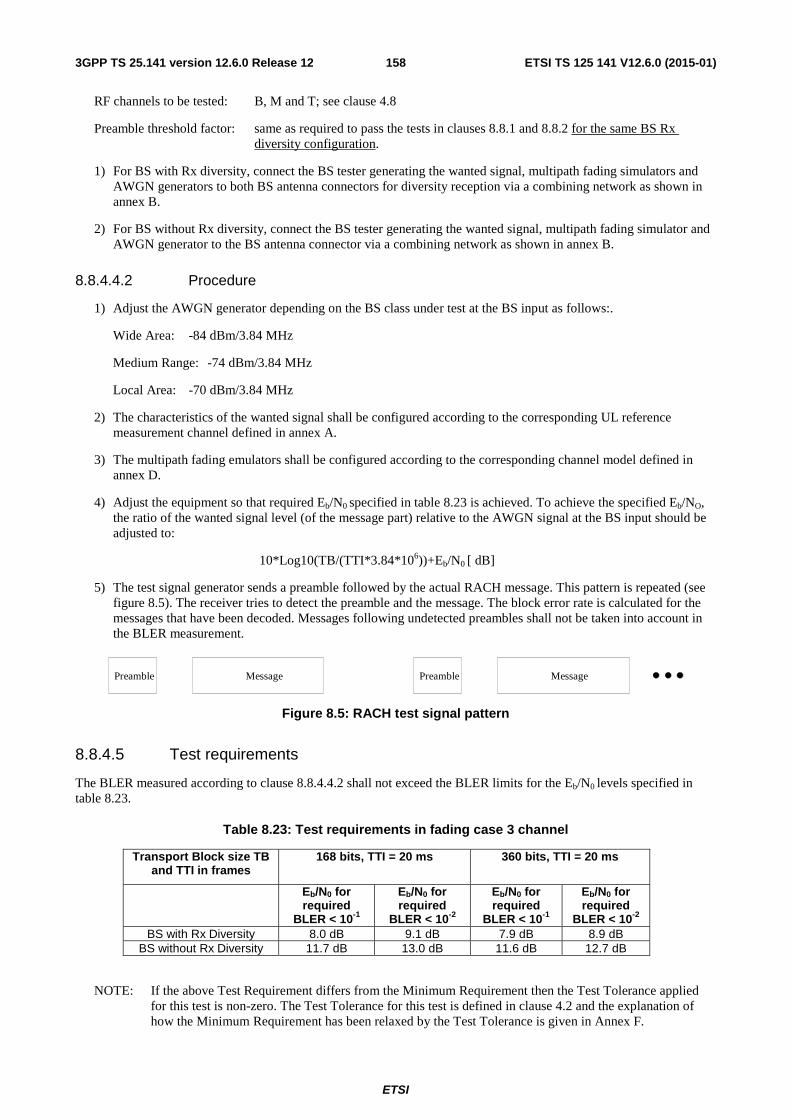
ETSI
ETSI TS 125 141 V12.6.0 (2015-01)1583GPP TS 25.141 version 12.6.0 Release 12
RF channels to be tested: B, M and T; see clause 4.8
Preamble threshold factor: same as required to pass the tests in clauses 8.8.1 and 8.8.2 for the same BS Rx diversity configuration.
1) For BS with Rx diversity, connect the BS tester generating the wanted signal, multipath fading simulators and AWGN generators to both BS antenna connectors for diversity reception via a combining network as shown in annex B.
2) For BS without Rx diversity, connect the BS tester generating the wanted signal, multipath fading simulator and AWGN generator to the BS antenna connector via a combining network as shown in annex B.
8.8.4.4.2 Procedure
1) Adjust the AWGN generator depending on the BS class under test at the BS input as follows:.
Wide Area: -84 dBm/3.84 MHz
Medium Range: -74 dBm/3.84 MHz
Local Area: -70 dBm/3.84 MHz
2) The characteristics of the wanted signal shall be configured according to the corresponding UL reference measurement channel defined in annex A.
3) The multipath fading emulators shall be configured according to the corresponding channel model defined in annex D.
4) Adjust the equipment so that required Eb/N0 specified in table 8.23 is achieved. To achieve the specified Eb/NO, the ratio of the wanted signal level (of the message part) relative to the AWGN signal at the BS input should be adjusted to:
10*Log10(TB/(TTI*3.84*106))+Eb/N0 [ dB]
5) The test signal generator sends a preamble followed by the actual RACH message. This pattern is repeated (see figure 8.5). The receiver tries to detect the preamble and the message. The block error rate is calculated for the messages that have been decoded. Messages following undetected preambles shall not be taken into account in the BLER measurement.
Preamble Message Preamble Message
Figure 8.5: RACH test signal pattern
8.8.4.5 Test requirements
The BLER measured according to clause 8.8.4.4.2 shall not exceed the BLER limits for the Eb/N0 levels specified in table 8.23.
Table 8.23: Test requirements in fading case 3 channel
Transport Block size TB and TTI in frames
168 bits, TTI = 20 ms 360 bits, TTI = 20 ms
Eb/N0 for required
BLER < 10-1
Eb/N0 for required
BLER < 10-2
Eb/N0 for required
BLER < 10-1
Eb/N0 for required
BLER < 10-2 BS with Rx Diversity 8.0 dB 9.1 dB 7.9 dB 8.9 dB
BS without Rx Diversity 11.7 dB 13.0 dB 11.6 dB 12.7 dB
NOTE: If the above Test Requirement differs from the Minimum Requirement then the Test Tolerance applied for this test is non-zero. The Test Tolerance for this test is defined in clause 4.2 and the explanation of how the Minimum Requirement has been relaxed by the Test Tolerance is given in Annex F.

ETSI
ETSI TS 125 141 V12.6.0 (2015-01)1593GPP TS 25.141 version 12.6.0 Release 12
8.8.5 Demodulation of RACH message in high speed train conditions
8.8.5.1 Definition and applicability
The performance requirement of RACH in high speed train conditions is determined by the maximum Block Error Ratio (BLER) allowed when the receiver input signal is at a specified Eb/N0 limit. The BLER is calculated for each of the measurement channels supported by the base station.
The requirement shall not be applied to Home BS.
The same preamble threshold factor as required to pass the tests in clauses 8.8.1, 8.8.2, and 8.8.2A shall be used for the same BS Rx diversity configuration. Only one signature is used and it is known by the receiver.
8.8.5.2 Minimum requirement
The minimum requirement is in TS 25.104 [1] clause 8.7.2.
8.8.5.3 Test purpose
The test shall verify the receiver"s ability to receive the test signal under multipath fading case 3 propagation conditions with a BLER not exceeding a specified limit.
8.8.5.4 Method of test
8.8.5.4.1 Initial conditions
Test environment: normal; see clause 4.4.1.
RF channels to be tested: B, M and T; see clause 4.8
Preamble threshold factor: same as required to pass the tests in clauses 8.8.1, 8.8.2, and 8.8.2A for the same BS Rx diversity configuration.
1) For BS with Rx diversity, connect the BS tester generating the wanted signal, multipath fading simulators and AWGN generators to both BS antenna connectors for diversity reception via a combining network as shown in annex B.
2) For BS without Rx diversity, connect the BS tester generating the wanted signal, multipath fading simulator and AWGN generator to the BS antenna connector via a combining network as shown in annex B.
8.8.5.4.2 Procedure
1) Adjust the AWGN generator depending on the BS class under test at the BS input as follows:.
Wide Area: -84 dBm/3.84 MHz
Medium Range: -74 dBm/3.84 MHz
Local Area: -70 dBm/3.84 MHz
2) The characteristics of the wanted signal shall be configured according to the corresponding UL reference measurement channel defined in annex A.
3) The multipath fading emulators shall be configured according to the corresponding channel model defined in annex D.
4) Adjust the equipment so that required Eb/N0 specified in table 8.23A is achieved. To achieve the specified Eb/NO, the ratio of the wanted signal level (of the message part) relative to the AWGN signal at the BS input should be adjusted to:
10*Log10(TB/(TTI*3.84*106))+Eb/N0 [ dB]

ETSI
ETSI TS 125 141 V12.6.0 (2015-01)1603GPP TS 25.141 version 12.6.0 Release 12
5) The test signal generator sends a preamble followed by the actual RACH message. This pattern is repeated (see figure 8.5A). The receiver tries to detect the preamble and the message. The block error rate is calculated for the messages that have been decoded. Messages following undetected preambles shall not be taken into account in the BLER measurement.
Preamble Message Preamble Message
Figure 8.5A: RACH test signal pattern
8.8.5.5 Test requirements
The BLER measured according to clause 8.8.5.4.2 shall not exceed the BLER limits for the Eb/N0 levels specified in table 8.23A.
Table 8.23A: Test requirements in high speed train conditions
Transport Block size TB and TTI in frames
168 bits, TTI = 20 ms 360 bits, TTI = 20 ms
Scenario Eb/N0 for required
BLER < 10-1
Eb/N0 for required
BLER < 10-2
Eb/N0 for required
BLER < 10-1
Eb/N0 for required
BLER < 10-2 1 BS with Rx
Diversity 5.7 dB 7.0 dB 5.9 dB 6.8 dB
BS without Rx Diversity
8.7 dB 10.0 dB 8.9 dB 9.8 dB
2 BS with Rx Diversity
n.a. n.a. n.a. n.a.
BS without Rx Diversity
8.3 dB 9.2 dB 8.0 dB 8.9 dB
3 BS with Rx Diversity
n.a. n.a. n.a. n.a.
BS without Rx Diversity
8.8 dB 10.2 dB 9.0 dB 9.9 dB
NOTE: If the above Test Requirement differs from the Minimum Requirement then the Test Tolerance applied for this test is non-zero. The Test Tolerance for this test is defined in clause 4.2 and the explanation of how the Minimum Requirement has been relaxed by the Test Tolerance is given in Annex F.
8.9 (void)
Table 8.24: (void)
Figure 8.6: (void)
Table 8.25: (void)
Table 8.26: (void)
Figure 8.7: (void)

ETSI
ETSI TS 125 141 V12.6.0 (2015-01)1613GPP TS 25.141 version 12.6.0 Release 12
Table 8.27: (void)
8.10 (void)
Table 8.28: (void)
Table 8.29: (void)
8.11 Performance of signalling detection for HS-DPCCH The performance requirement of HS-DPCCH signalling detection is determined by the two parameters: the probability of false detection of ACK; P(DTX->ACK) and the probability of mis-detection of ACK; P(ACK->DTX or NACK).
8.11.1 ACK false alarm in static propagation conditions
8.11.1.1 Definition and applicability
ACK false alarm is defined as a conditional probability of erroneous detection of ACK when input is only DPCCH and DPDCH (+interference). The performance requirement of ACK false alarm in static propagation conditions is determined by the maximum error ratio allowed when the receiver input signal is at a specified Ec/N0 limit. ACK false alarm: P(DTX->ACK) shall be 10-2 or less.
8.11.1.2 Minimum requirement
The minimum requirement is in TS 25.104 [1] clause 8.10.1.
Table 8.30: (void)
8.11.1.3 Test purpose
The test shall verify the receiver's ability to detect HS-DPCCH signalling (ACK/NACK) under static propagation conditions.
8.11.1.4 Method of test
8.11.1.4.1 Initial conditions
Test environment: normal; see clause 4.4.1.
RF channels to be tested: B, M and T; see clause 4.8
1) Connect the BS tester generating the wanted signal and AWGN generators to both BS antenna connectors for diversity reception via a combining network as shown in annex B.
8.11.1.4.2 Procedure
1) Adjust the AWGN generator depending on the BS class under test at the BS input as follows:.
Wide Area: -84 dBm/3.84 MHz
Medium Range: -74 dBm/3.84 MHz
Local Area / Home BS: -70 dBm/3.84 MHz
2) The characteristics of the wanted signal shall be configured according to the corresponding UL reference measurement channel defined in annex A.

ETSI
ETSI TS 125 141 V12.6.0 (2015-01)1623GPP TS 25.141 version 12.6.0 Release 12
3) Adjust the equipment so that required Ec/N0 specified in table 8.31 is achieved. To achieve the specified Ec/N0, the ratio of the wanted signal level relative to the AWGN signal at the BS input should be adjusted to: Ec/N0
[ dB].
4) The test signal generator sends only DPCCH and DPDCH. The receiver tries to detect HS-DPCCH signalling. The ACK false detection rate should be measured only on those slots corresponding to the ACK/NACK field of HS-DPCCH.
8.11.1.5 Test requirements
ACK false alarm, P(DTX->ACK) shall not exceed the limits for the Ec/N0 specified in Table 8.31.
Table 8.31: Performance requirements for ACK false alarm in AWGN channel
Received Ec/N0 Required error ratio -19.5 dB < 10-2
NOTE: If the above Test Requirement differs from the Minimum Requirement then the Test Tolerance applied for this test is non-zero. The Test Tolerance for this test is defined in clause 4.2 and the explanation of how the Minimum Requirement has been relaxed by the Test Tolerance is given in Annex F.
8.11.2 ACK false alarm in multipath fading conditions
8.11.2.1 Definition and applicability
ACK false alarm is defined as a conditional probability of erroneous detection of ACK when input is only DPCCH and DPDCH (+interference). The performance requirement of ACK false alarm in multipath fading conditions is determined by the maximum error ratio allowed when the receiver input signal is at a specified Ec/N0 limit. ACK false alarm: P(DTX->ACK) shall be 10-2 or less.
Only test in Case 1 shall be applied to Home BS.
8.11.2.2 Minimum requirement
The minimum requirement is in TS 25.104 [1] clause 8.10.1.
Table 8.32: (void)
8.11.2.3 Test purpose
The test shall verify the receiver's ability to detect HS-DPCCH signalling (ACK/NACK) under multipath fading case 3 propagation conditions.
8.11.2.4 Method of test
8.11.2.4.1 Initial conditions
Test environment: normal; see clause 4.4.1.
RF channels to be tested: B, M and T; see clause 4.8
1) Connect the BS tester generating the wanted signal, multipath fading simulators and AWGN generators to both BS antenna connectors for diversity reception via a combining network as shown in annex B.
8.11.2.4.2 Procedure
1) Adjust the AWGN generator depending on the BS class under test at the BS input as follows:
Wide Area: -84 dBm/3.84 MHz

ETSI
ETSI TS 125 141 V12.6.0 (2015-01)1633GPP TS 25.141 version 12.6.0 Release 12
Medium Range: -74 dBm/3.84 MHz
Local Area / Home BS: -70 dBm/3.84 MHz
2) The characteristics of the wanted signal shall be configured according to the corresponding UL reference measurement channel defined in annex A.
3) The multipath fading emulators shall be configured according to the corresponding channel model defined in annex D.
4) Adjust the equipment so that required Ec/N0 specified in table 8.33 is achieved. To achieve the specified Ec/N0, the ratio of the wanted signal level relative to the AWGN signal at the BS input should be adjusted to: Ec/N0
[ dB].
5) The test signal generator sends only DPCCH and DPDCH. The receiver tries to detect HS-DPCCH signalling. The ACK false detection rate should be measured only on those slots corresponding to the ACK/NACK field of HS-DPCCH..
8.11.2.5 Test requirements
ACK false alarm, P(DTX->ACK) shall not exceed the limits for the Ec/N0 specified in Table 8.33.
Table 8.33: Performance requirements for ACK false alarm in fading channels
Propagation conditions Received Ec/N0 Required error ratio Case 1 -12.5 dB < 10-2 Case 2* -15.4 dB < 10-2 Case 3* -17.2 dB < 10-2
* Not applicable for Home BS
NOTE: If the above Test Requirement differs from the Minimum Requirement then the Test Tolerance applied for this test is non-zero. The Test Tolerance for this test is defined in clause 4.2 and the explanation of how the Minimum Requirement has been relaxed by the Test Tolerance is given in Annex F.
8.11.3 ACK mis-detection in static propagation conditions
8.11.3.1 Definition and applicability
The probability of ACK mis-detection is defined a probability of ACK mis-detected when ACK is transmitted. The performance requirement of ACK mis-detection in static propagation conditions is determined by the maximum error ratio allowed when the receiver input signal is at a specified Ec/N0 limit.
8.11.3.2 Minimum requirement
The minimum requirement is in TS 25.104 [1] clause 8.10.2.
Table 8.34: (void)
8.11.3.3 Test purpose
The test shall verify the receiver"s ability to receive the test signal under static propagation conditions with an error ratio not exceeding a specified limit.
8.11.3.4 Method of test
8.11.3.4.1 Initial conditions
Test environment: normal; see clause 4.4.1.
RF channels to be tested: B, M and T; see clause 4.8

ETSI
ETSI TS 125 141 V12.6.0 (2015-01)1643GPP TS 25.141 version 12.6.0 Release 12
1) Connect the BS tester generating the wanted signal and AWGN generators to both BS antenna connectors for diversity reception via a combining network as shown in annex B.
8.11.3.4.2 Procedure
1) Adjust the AWGN generator depending on the BS class under test at the BS input as follows:
Wide Area: -84 dBm/3.84 MHz
Medium Range: -74 dBm/3.84 MHz
Local Area / Home BS: -70 dBm/3.84 MHz
2) The characteristics of the wanted signal shall be configured according to the corresponding UL reference measurement channel defined in annex A.
3) Adjust the equipment so that required Ec/N0 specified in table 8.35 is achieved. To achieve the specified Ec/N0, the ratio of the wanted signal level relative to the AWGN signal at the BS input should be adjusted to: Ec/N0
[ dB].
4) The test signal generator sends the ACKs and CQIs with DPCCH/DPDCH. The receiver tries to detect HS-DPCCH signalling. The ACK mis-detection rate should be measured only on those slots corresponding to the ACK/NACK field of HS-DPCCH..
8.11.3.5 Test requirements
The probability of ACK mis-detection, P(ACK->NACK or DTX) (= mis-detected when ACK is transmitted) shall not exceed the required error ratio for the Ec/N0 specified in Table 8.35.
Table 8.35: Performance requirements for ACK mis-detection in AWGN channel
Received Ec/N0 Required error ratio -16.9 dB < 10-2
NOTE: If the above Test Requirement differs from the Minimum Requirement then the Test Tolerance applied for this test is non-zero. The Test Tolerance for this test is defined in clause 4.2 and the explanation of how the Minimum Requirement has been relaxed by the Test Tolerance is given in Annex F.
8.11.4 ACK mis-detection in multipath fading conditions
8.11.4.1 Definition and applicability
The probability of ACK mis-detection is defined a probability of ACK mis-detected when ACK is transmitted. The performance requirement of ACK mis-detection in multipath fading conditions is determined by the maximum error ratio allowed when the receiver input signal is at a specified Ec/N0 limit.
Only test in Case 1 shall be applied to Home BS.
8.11.4.2 Minimum requirement
The minimum requirement is in TS 25.104 [1] clause 8.10.2.
Table 8.36: (void)
8.11.4.3 Test purpose
The test shall verify the receiver"s ability to receive the test signal under multipath fading propagation conditions with an error ratio not exceeding a specified limit.

ETSI
ETSI TS 125 141 V12.6.0 (2015-01)1653GPP TS 25.141 version 12.6.0 Release 12
8.11.4.4 Method of test
8.11.4.4.1 Initial conditions
Test environment: normal; see clause 4.4.1.
RF channels to be tested: B, M and T; see clause 4.8
1) BS antenna connectors for diversity reception via a combining network as shown in annex B.
8.11.4.4.2 Procedure
1) Adjust the AWGN generator depending on the BS class under test at the BS input as follows:.
Wide Area: -84 dBm/3.84 MHz
Medium Range: -74 dBm/3.84 MHz
Local Area / Home BS: -70 dBm/3.84 MHz
2) The characteristics of the wanted signal shall be configured according to the corresponding UL reference measurement channel defined in annex A.
3) The multipath fading emulators shall be configured according to the corresponding channel model defined in annex D.
4) Adjust the equipment so that required Ec/N0 specified in table 8.37 is achieved. To achieve the specified Ec/N0, the ratio of the wanted signal level relative to the AWGN signal at the BS input should be adjusted to: Ec/N0
[ dB]
5) The test signal generator sends the ACKs and CQIs with DPCCH/DPDCH. The receiver tries to detect HS-DPCCH signalling. The ACK mis-detection rate should be measured only on those slots corresponding to the ACK/NACK field of HS-DPCCH.
8.11.4.5 Test requirements
The probability of ACK mis-detection, P(ACK->NACK or DTX) (= mis-detected when ACK is transmitted) shall not exceed the required error ratio for the Ec/N0 specified in Table 8.37.
Table 8.37: Performance requirements for ACK mis-detection in fading channels
Propagation conditions Received Ec/N0 Required error ratio Case 1 -10.1 dB < 10-2 Case 2* -13.0 dB < 10-2 Case 3* -11.5 dB < 10-2
* Not applicable for Home BS
NOTE: If the above Test Requirement differs from the Minimum Requirement then the Test Tolerance applied for this test is non-zero. The Test Tolerance for this test is defined in clause 4.2 and the explanation of how the Minimum Requirement has been relaxed by the Test Tolerance is given in Annex F.
8.11A Performance of signalling detection for 4C-HSDPA HS-DPCCH
This test shall be performed only for the BS supporting 4C-HSDPA. The performance requirement of 4C-HSDPA HS-DPCCH signalling detection is determined by the two parameters:
(i) The probability of ACK false alarm for each stream, P(DTX ->ACK) (=false ACK detection for a given stream in the detected HARQ message given that no HARQ message is transmitted)

ETSI
ETSI TS 125 141 V12.6.0 (2015-01)1663GPP TS 25.141 version 12.6.0 Release 12
(ii) The probability of ACK mis-detection for each stream, P(ACK->NACK, DTX (no transmission) or DTX codeword) (=an ACK for a given stream in a transmitted HARQ message is mis-detected as a NACK or DTX (no transmission) or DTX codeword in the received HARQ message)
Performance requirements of HS-DPCCH signaling detection for 4C-HSDPA apply also for HSDPA Multiflow operation on three/four cells on two frequencies without MIMO. If tested NodeB supports both 4C-HSDPA and HSDPA Multiflow operation on three/four cells on two frequencies without MIMO, this test shall be performed only once.
The appropriate codebook subset is chosen for testing.
8.11A.1 ACK false alarm for 4C-HSDPA in static propagation conditions
8.11A.1.1 Definition and applicability
ACK false alarm for 4C-HSDPA HS-DPCCH is defined as in Section 8.11A when input is only DPCCH and DPDCH (+interference). The performance requirement of ACK false alarm in static propagation conditions is determined by the maximum error ratio allowed when the receiver input signal is at a specified Ec/N0 limit. ACK false alarm shall be 10-2 or less.
8.11A.1.2 Minimum requirement
The minimum requirement is in TS 25.104 [1] clause 8.10A.1.1
8.11A.1.3 Test purpose
The test shall verify the receiver's ability to detect 4C-HSDPA UL HS-DPCCH signalling (ACK/NACK) under static propagation conditions.
8.11A.1.4 Method of test
8.11A.1.4.1 Initial conditions
Test environment: normal; see clause 4.4.1.
RF channels to be tested: B, M and T; see clause 4.8
1) Connect the BS tester generating the wanted signal and AWGN generators to both BS antenna connectors for diversity reception via a combining network as shown in Annex B.3.1.
8.11A.1.4.2 Procedure
1) Adjust the AWGN generator depending on the BS class under test at the BS input as follows:.
Wide Area: -84 dBm/3.84 MHz
Medium Range: -74 dBm/3.84 MHz
Local Area / Home BS: -70 dBm/3.84 MHz
2) The characteristics of the wanted signal shall be configured according to the corresponding UL reference measurement channel defined in Annex A.9A.
3) Adjust the equipment so that required Ec/N0 specified in Table 8.11A.1 is achieved. To achieve the specified Ec/N0, the ratio of the wanted signal level relative to the AWGN signal at the BS input should be adjusted to: Ec/N0 [dB].
4) The test signal generator sends only DPCCH and DPDCH. The receiver tries to detect HS-DPCCH signalling. The ACK false detection rate should be measured only on those slots corresponding to the ACK/NACK field of HS-DPCCH.

ETSI
ETSI TS 125 141 V12.6.0 (2015-01)1673GPP TS 25.141 version 12.6.0 Release 12
8.11A.1.5 Test requirements
The probability of ACK false alarm for each stream shall not exceed the required error ratio for the Ec/N0 specified in Table 8.11A.1.
Table 8.11A.1: Performance requirements for ACK false alarm per stream in static conditions
Carrier Configuration1
Propagation condition
Received Ec/N0 [dB] (Test condition) For BS with Rx Diversity
Required error ratio
4/4/4 Static -16.3 < 10-2 4/2/2 Static -16.3 < 10-2 3/3/3 Static -16.6 < 10-2 3/2/1 Static -16.6 < 10-2 3/3/0 Static -17.0 < 10-2
Note: Carrier configuration X/Y/Z denotes X number of carriers configured, Y number of active carriers, and Z number of carriers configured as MIMO out of Y carriers.
NOTE: If the above Test Requirement differs from the Minimum Requirement then the Test Tolerance applied for this test is non-zero. The Test Tolerance for this test is defined in clause 4.2 and the explanation of how the Minimum Requirement has been relaxed by the Test Tolerance is given in Annex F.
8.11A.2 ACK false alarm for 4C-HSDPA in multipath fading conditions
8.11A.2.1 Definition and applicability
ACK false alarm for 4C-HSDPA HS-DPCCH is defined as in Section 8.11A when input is only DPCCH and DPDCH (+interference). The performance requirement of ACK false alarm in multipath fading conditions is determined by the maximum error ratio allowed when the receiver input signal is at a specified Ec/N0 limit. ACK false alarm: P(DTX->ACK) shall be 10-2 or less.
8.11A.2.2 Minimum requirement
The minimum requirement is in TS 25.104 [1] clause 8.10A.1.1.
8.11A.2.3 Test purpose
The test shall verify the receiver's ability to detect 4C-HSDPA HS-DPCCH signalling (ACK/NACK) under multipath fading case 1 propagation conditions.
8.11A.2.4 Method of test
8.11A.2.4.1 Initial conditions
Test environment: normal; see clause 4.4.1.
RF channels to be tested: B, M and T; see clause 4.8
1) Connect the BS tester generating the wanted signal, multipath fading simulators and AWGN generators to both BS antenna connectors for diversity reception via a combining network as shown in Annex B.3.2.
8.11A.2.4.2 Procedure
1) Adjust the AWGN generator depending on the BS class under test at the BS input as follows:
Wide Area: -84 dBm/3.84 MHz
Medium Range: -74 dBm/3.84 MHz

ETSI
ETSI TS 125 141 V12.6.0 (2015-01)1683GPP TS 25.141 version 12.6.0 Release 12
Local Area / Home BS: -70 dBm/3.84 MHz
2) The characteristics of the wanted signal shall be configured according to the corresponding UL reference measurement channel defined in Annex A.9A.
3) The multipath fading emulators shall be configured according to the corresponding channel model defined in Annex D.
4) Adjust the equipment so that required Ec/N0 specified in Table 8.11A.2 is achieved. To achieve the specified Ec/N0, the ratio of the wanted signal level relative to the AWGN signal at the BS input should be adjusted to: Ec/N0 [ dB].
5) The test signal generator sends only DPCCH and DPDCH. The receiver tries to detect HS-DPCCH signalling. The ACK false detection rate should be measured only on those slots corresponding to the ACK/NACK field of HS-DPCCH..
8.11A.2.5 Test requirements
The probability of ACK false alarm for each stream shall not exceed the required error ratio for the Ec/N0 specified in Table 8.11A.2
Table 8.11A.2: Performance requirements for ACK false alarm per stream in multipath conditions
Carrier Configuration1
Propagation condition
Received Ec/N0 [dB] (Test condition) For BS with Rx Diversity
Required error ratio
4/4/4 Case 1 -10.8 < 10-2 4/2/2 Case 1 -10.8 < 10-2 3/3/3 Case 1 -10.8 < 10-2 3/2/1 Case 1 -10.8 < 10-2 3/3/0 Case 1 -11.9 < 10-2
Note: Carrier configuration X/Y/Z denotes X number of carriers configured, Y number of active carriers, and Z number of carriers configured as MIMO out of Y carriers.
NOTE: If the above Test Requirement differs from the Minimum Requirement then the Test Tolerance applied for this test is non-zero. The Test Tolerance for this test is defined in clause 4.2 and the explanation of how the Minimum Requirement has been relaxed by the Test Tolerance is given in Annex F.
8.11A.3 ACK mis-detection for 4C-HSDPA in static propagation conditions
8.11A.3.1 Definition and applicability
The probability of ACK mis-detection for each stream, P(ACK->NACK, DTX (no transmission) or DTX codeword) (=an ACK for a given stream in a transmitted HARQ message is mis-detected as a NACK or DTX (no transmission) or DTX codeword in the received HARQ message) shall not exceed the required error ratio for the Ec/N0 specified in Table 8.11A.3. This requirement shall be conditioned on that the ACK false alarm requirement in Table 8.11A.1. above shall also be concurrently satisfied.
The performance requirement of ACK mis-detection in static propagation conditions is determined by the maximum error ratio allowed when the receiver input signal is at a specified Ec/N0 limit.
8.11A.3.2 Minimum requirement
The minimum requirement is in TS 25.104 [1] clause 8.10A.1.2.
8.11A.3.3 Test purpose
The test shall verify the receiver"s ability to receive the test signal under static propagation conditions with an error ratio not exceeding a specified limit.
ETSI
ETSI TS 125 141 V12.6.0 (2015-01)1693GPP TS 25.141 version 12.6.0 Release 12
8.11A.3.4 Method of test
8.11A.3.4.1 Initial conditions
Test environment: normal; see clause 4.4.1.
RF channels to be tested: B, M and T; see clause 4.8
1) Connect the BS tester generating the wanted signal and AWGN generators to both BS antenna connectors for diversity reception via a combining network as shown in Annex B.3.1.
8.11A.3.4.2 Procedure
1) Adjust the AWGN generator depending on the BS class under test at the BS input as follows:
Wide Area: -84 dBm/3.84 MHz
Medium Range: -74 dBm/3.84 MHz
Local Area / Home BS: -70 dBm/3.84 MHz
2) The characteristics of the wanted signal shall be configured according to the corresponding UL reference measurement channel defined in Annex A.9A.
3) Adjust the equipment so that required Ec/N0 specified in Table 8.11A.3 is achieved. To achieve the specified Ec/N0, the ratio of the wanted signal level relative to the AWGN signal at the BS input should be adjusted to: Ec/N0 [dB].
4) The test signal generator sends the ACKs with DPCCH/DPDCH. The receiver tries to detect HS-DPCCH signalling. The ACK mis-detection rate should be measured only on those slots corresponding to the ACK/NACK field of HS-DPCCH.
8.11A.3.5 Test requirements
The probability of ACK mis-detection shall not exceed the required error ratio for the Ec/N0 specified in Table 8.11A.3.
Table 8.11A.3: Performance requirements for ACK mis-detection per stream conditioned on ACK false alarm per stream is less than 1%.
Carrier Configuration1
Propagation condition
Received Ec/N0 [dB] (Test condition) For BS with Rx Diversity
Required error ratio
4/4/4 Static -13.5 < 10-2 4/2/2 Static -14.0 < 10-2 3/3/3 Static -13.8 < 10-2 3/2/1 Static -14.6 < 10-2 3/3/0 Static -15.0 < 10-2
Note: Carrier configuration X/Y/Z denotes X number of carriers configured, Y number of active carriers, and Z number of carriers configured as MIMO out of Y carriers.
NOTE: If the above Test Requirement differs from the Minimum Requirement then the Test Tolerance applied for this test is non-zero. The Test Tolerance for this test is defined in clause 4.2 and the explanation of how the Minimum Requirement has been relaxed by the Test Tolerance is given in Annex F.
8.11A.4 ACK mis-detection for 4C-HSDPA in multipath fading conditions
8.11A.4.1 Definition and applicability
The probability of ACK mis-detection for each stream, P(ACK->NACK, DTX (no transmission) or DTX codeword) (=an ACK for a given stream in a transmitted HARQ message is mis-detected as a NACK or DTX (no transmission) or

ETSI
ETSI TS 125 141 V12.6.0 (2015-01)1703GPP TS 25.141 version 12.6.0 Release 12
DTX codeword in the received HARQ message) shall not exceed the required error ratio for the Ec/N0 specified in Table 8.11A.4. This requirement shall be conditioned on that the ACK false alarm requirement in Table 8.11A.2. above shall also be concurrently satisfied.
The performance requirement of ACK mis-detection in multipath fading conditions is determined by the maximum error ratio allowed when the receiver input signal is at a specified Ec/N0 limit.
8.11A.4.2 Minimum requirement
The minimum requirement is in TS 25.104 [1] clause 8.10A.1.2.
8.11A.4.3 Test purpose
The test shall verify the receiver"s ability to receive the test signal under multipath fading propagation conditions with an error ratio not exceeding a specified limit.
8.11A.4.4 Method of test
8.11A.4.4.1 Initial conditions
Test environment: normal; see clause 4.4.1.
RF channels to be tested: B, M and T; see clause 4.8
1) BS antenna connectors for diversity reception via a combining network as shown in Annex B.3.2
8.11A.4.4.2 Procedure
1) Adjust the AWGN generator depending on the BS class under test at the BS input as follows:.
Wide Area: -84 dBm/3.84 MHz
Medium Range: -74 dBm/3.84 MHz
Local Area / Home BS: -70 dBm/3.84 MHz
2) The characteristics of the wanted signal shall be configured according to the corresponding UL reference measurement channel defined in Annex A.9A.
3) The multipath fading emulators shall be configured according to the corresponding channel model defined in Annex D.
4) Adjust the equipment so that required Ec/N0 specified in Table 8.11A.4 is achieved. To achieve the specified Ec/N0, the ratio of the wanted signal level relative to the AWGN signal at the BS input should be adjusted to: Ec/N0 [ dB]
5) The test signal generator sends the ACKs with DPCCH/DPDCH. The receiver tries to detect HS-DPCCH signalling. The ACK mis-detection rate should be measured only on those slots corresponding to the ACK/NACK field of HS-DPCCH.
8.11A.4.5 Test requirements
The probability of ACK mis-detection shall not exceed the required error ratio for the Ec/N0 specified in Table 8.11A.4.

ETSI
ETSI TS 125 141 V12.6.0 (2015-01)1713GPP TS 25.141 version 12.6.0 Release 12
Table 8.11A.4: Performance requirements for ACK mis-detection per stream conditioned on ACK false alarm per stream is less than 1%.
Carrier Configuration1
Propagation condition
Received Ec/N0 [dB] (Test condition) For BS with Rx Diversity
Required error ratio
4/4/4 Case 1 -8.1 < 10-2 4/2/2 Case 1 -8.4 < 10-2 3/3/3 Case 1 -8.0 < 10-2 3/2/1 Case 1 -8.2 < 10-2 3/3/0 Case 1 -9.9 < 10-2
Note: Carrier configuration X/Y/Z denotes X number of carriers configured, Y number of active carriers, and Z number of carriers configured as MIMO out of Y carriers.
NOTE: If the above Test Requirement differs from the Minimum Requirement then the Test Tolerance applied for this test is non-zero. The Test Tolerance for this test is defined in clause 4.2 and the explanation of how the Minimum Requirement has been relaxed by the Test Tolerance is given in Annex F.
8.11B Performance of signalling detection for 8C-HSDPA HS-DPCCH
This test shall be performed only for the BS supporting 8C-HSDPA.
In 8C-HSDPA two identical HS-DPCCH channels similar to the 4C-HSDPA HS-DPCCH are used and they are transmitted by means of I/Q multiplexing. One HS-DPCCH is dedicated to carriers 1 to 4, while the other to carriers 5 to 8. The same test requirements as for 4C-HSDPA HS-DPCCH, as defined in section 8.11A, shall be fulfilled for both I and Q HS-DPCCH channels.
The appropriate codebook subset is chosen for testing.
8.12 Demodulation of E-DPDCH in multipath fading conditions
8.12.1 Definition and applicability
The performance requirement of the E-DPDCH in multi path fading condition is determined by the minimum throughput, R. Test parameters are specified in Table 8.38.
For a BS supporting DC-HSUPA the requirements for FRC1, FRC2, FRC3 and FRC8 shall apply on each cell.
Table 8.38: Test parameters for testing E-DPDCH
Parameter Unit Test RSN {0, 1, 2, 3}
HARQ combining IR Maximum number of HARQ transmission 4
Power control OFF
DPCCH slot format
FRC8 or BS supporting
DC-HSUPA 1
Otherwise 0 E-DPCCH # code words
1024, no optimization based on prior knowledge of valid code words.
Physical channels to be turned on DPCCH, E-DPDCH and E-DPCCH
Only tests in Pedestrian A shall be applied to Home BS.

ETSI
ETSI TS 125 141 V12.6.0 (2015-01)1723GPP TS 25.141 version 12.6.0 Release 12
8.12.2 Minimum requirement
The minimum requirement is in TS 25.104 [1] clause 8.11.
Table 8.39: (void)
8.12.3 Test Purpose
The test shall verify the receiver's ability to receive the test signal under slow multipath fading propagation conditions with a throughput not below a specified limit.
8.12.4 Method of test
8.12.4.1 Initial conditions
Test environment: normal; see clause 4.4.1.
RF channels to be tested: B, M and T; see clause 4.8
1) For BS with Rx diversity, connect the BS tester generating the wanted signal, multipath fading simulators and AWGN generators to both BS antenna connectors for diversity reception via a combining network as shown in annex B.
2) For BS without Rx diversity, connect the BS tester generating the wanted signal, multipath fading simulator and AWGN generator to the BS antenna connector via a combining network as shown in annex B.
8.12.4.2 Procedure
1) Adjust the AWGN generator depending on the BS class under test at the BS input as follows:.
Wide Area: -84 dBm/3.84 MHz
Medium Range: -74 dBm/3.84 MHz
Local Area / Home BS: -70 dBm/3.84 MHz
2) The characteristics of the wanted signal shall be configured according to the corresponding UL reference measurement channel defined in annex A.
3) The multipath fading emulators shall be configured according to the corresponding channel model defined in annex D.
4) Adjust the equipment so that required EC/N0 specified in table 8.40 is achieved.
5) For each of the reference channels in table 8.40 applicable for the base station, measure the throughput.
8.12.4.3 Test requirements
The throughput measured according to clause 8.12.4.2 shall not be below the limits for the EC/N0 levels specified in table 8.40.

ETSI
ETSI TS 125 141 V12.6.0 (2015-01)1733GPP TS 25.141 version 12.6.0 Release 12
Table 8.40: Test Requirement for E-DPDCH
NOTE: If the above Test Requirement differs from the Minimum Requirement then the Test Tolerance applied for this test is non-zero. The Test Tolerance for this test is defined in clause 4.2 and the explanation of how the Minimum Requirement has been relaxed by the Test Tolerance is given in Annex F.
8.12A Demodulation of E-DPDCH and S-E-DPDCH in multipath fading conditions for UL MIMO
8.12A.1 Definition and applicability
The performance requirements of the E-DPDCH and S-E-DPDCH in multi path fading condition for UL MIMO are determined by the minimum throughput, R. Test parameters are specified in Table 8.38A.
Table 8.38A: Test parameters for testing E-DPDCH and S-E-DPDCH for UL MIMO
Parameter Test
RSN {0, 1, 2, 3} HARQ combining IR
Maximum number of HARQ transmission 4
Power control OFF TX weight vector selection A fixed precoding weight vector
Physical channels to be turned on DPCCH, S-DPCCH, E-DPCCH, S-E-
DPCCH, E-DPDCH and S-E-DPDCH
8.12A.2 Minimum requirement
The minimum requirement is in TS 25.104 [1] clause 8.11A.
Fixed Reference Channel
Reference value, EC/N0 (dB), for R ≥ 30% and R ≥ 70% of maximum information bit rate
Propagation conditionsPropagation
conditions FRC1 FRC2 FRC3 FRC4 FRC5 FRC6 FRC7
FRC8 Non
E-DPCCH boosting
E-DPCCH Boosting
Pedestrian A
without RX diversity 30% -1.8 1.4 3.0 -6.5 -3.8 -0.8 -14.4 NA NA 70% 4.3 7.7 9.7 0.0 2.7 5.8 -7.8 16.8 17.5
Pedestrian A with RX diversity
30% -5.6 -2.5 -0.8 -10.0 -7.4 -4.4 -17.7 NA NA 70% -0.4 2.8 4.7 -4.6 -2.0 0.8 -12.7 10.7 11.0
Pedestrian B without RX diversity*
30% -1.9 1.7 4.1 -6.9 -4.1 -0.7 -13.0 NA NA 70% 4.5 NA NA -1.5 1.5 5.9 -9.5 NA NA
Pedestrian B with RX diversity*
30% -5.5 -2.5 -0.4 -10.1 -7.5 -4.3 -17.4 NA NA 70% 0.3 4.5 8.8 -5.1 -2.3 1.3 -13.2 13.0 13.7
Vehicular 30 without RX diversity*
30% -1.9 1.6 3.8 -6.9 -4.0 -0.8 -13.7 NA NA 70% 5.5 NA NA -1.1 2.0 6.4 -9.5 NA NA
Vehicular 30 with RX diversity*
30% -5.5 -2.3 -0.3 -10.1 -7.4 -4.3 -17.0 NA NA 70% 1.2 5.3 9.4 -4.8 -2.0 1.6 -13.1 13.9 14.2
Vehicular 120 without RX diversity*
30% -1.5 1.9 4.2 -6.7 -3.6 -0.6 -13.4 NA NA 70% 5.7 NA NA -0.7 2.1 6.7 -9.5 NA NA
Vehicular 120 with RX diversity*
30% -5.1 -2.0 0.1 -9.8 -7.0 -3.7 -16.4 NA NA 70% 1.3 5.6 10.1 -4.5 -1.7 1.8 -12.6 NA NA
* Not applicable for Home BS

ETSI
ETSI TS 125 141 V12.6.0 (2015-01)1743GPP TS 25.141 version 12.6.0 Release 12
8.12A.3 Test Purpose
The test shall verify the receiver's ability to receive the test signal under slow multipath fading propagation conditions with a throughput not below a specified limit.
8.12A.4 Method of test
8.12A.4.1 Initial conditions
Test environment: normal; see clause 4.4.1.
RF channels to be tested: B, M and T; see clause 4.8
For BS with Rx diversity, connect the BS tester generating the wanted signal, multipath fading simulators and AWGN generators to both BS antenna connectors for diversity reception via a combining network as shown in annex B.
8.12A.4.2 Procedure
1) Adjust the AWGN generator depending on the BS class under test at the BS input as follows:.
Wide Area: -84 dBm/3.84 MHz
Medium Range: -74 dBm/3.84 MHz
Local Area / Home BS: -70 dBm/3.84 MHz
2) The characteristics of the wanted signal shall be configured according to the corresponding UL reference measurement channel defined in annex A.
3) The multipath fading emulators shall be configured according to the corresponding channel model defined in annex D.
4) Adjust the equipment so that required EC/N0 specified in table 8.40A is achieved.
5) For each of the reference channels in table 8.40A applicable for the base station, measure the throughput.
8.12A.4.3 Test requirements
The throughput measured according to clause 8.12A.4.2 shall not be below the limits for the EC/N0 levels specified in table 8.40A.
Table 8.40A: Test Requirement for E-DPDCH and S-E-DPDCH for UL MIMO
Fixed Reference Channel
Reference value, EC/N0 (dB), for R ≥ 70% of maximum information bit rate
Propagation conditions FRC9 FRC10
E-DPDCH S-E-DPDCH E-DPDCH S-E-DPDCH
Ped A, 3 km/h 9.7 9.7 18.4 18.4
Veh A, 3 km/h 11.0 11.0 N/A N/A
NOTE: If the above Test Requirement differs from the Minimum Requirement then the Test Tolerance applied for this test is non-zero. The Test Tolerance for this test is defined in clause 4.2 and the explanation of how the Minimum Requirement has been relaxed by the Test Tolerance is given in Annex F.

ETSI
ETSI TS 125 141 V12.6.0 (2015-01)1753GPP TS 25.141 version 12.6.0 Release 12
8.13 Performance of signalling detection for E-DPCCH in multipath fading conditions
The performance requirement of E-DPCCH signalling detection is determined by the two parameters: the probability of false detection of codeword; P(DTX -> codeword) and the probability of missed detection of codeword; P(codeword -> DTX).
Table 8.41: Test parameters for testing E-DPCCH
Parameter Unit Test Power control Off
E-DPCCH # code words 1024, no optimization based on prior knowledge of valid code words.
Physical channels to be turned on for missed detection test
DPCCH, E-DPDCH and E-DPCCH
Physical channels to be turned on for false alarm test
DPCCH
8.13.1 E-DPCCH false alarm in multipath fading conditions
8.13.1.1 Definition and applicability
E-DPCCH false alarm is defined as a conditional probability of detection of codeword when input is only DPCCH (+interference). The E-DPDCH and E-DPCCH is turned off. The performance requirement of E-DPCCH false alarm in multipath fading conditions is determined by the maximum detection probability allowed when the receiver input signal is at a specified Ec/N0 limit. E-DPCCH false alarm: P(DTX -> codeword) shall be 10-2 or less.
Only tests in Pedestrian A shall be applied to Home BS.
8.13.1.2 Minimum requirement
The minimum requirement is in TS 25.104 [1] clause 8.12.
Table 8.42: (void)
8.13.1.3 Test purpose
The test shall verify the receiver's ability to detect E-DPCCH signalling under multipath fading propagation conditions.
8.13.1.4 Method of test
8.13.1.4.1 Initial conditions
Test environment: normal; see clause 4.4.1.
RF channels to be tested: B, M and T; see clause 4.8
1) For BS with Rx diversity, connect the BS tester generating the wanted signal, multipath fading simulators and AWGN generators to both BS antenna connectors for diversity reception via a combining network as shown in annex B.
2) For BS without Rx diversity, connect the BS tester generating the wanted signal, multipath fading simulator and AWGN generator to the BS antenna connector via a combining network as shown in annex B.
8.13.1.4.2 Procedure
1) Adjust the AWGN generator depending on the BS class under test at the BS input as follows:
Wide Area: -84 dBm/3.84 MHz

ETSI
ETSI TS 125 141 V12.6.0 (2015-01)1763GPP TS 25.141 version 12.6.0 Release 12
Medium Range: -74 dBm/3.84 MHz
Local Area / Home BS: -70 dBm/3.84 MHz
2) The characteristics of the wanted signal shall be configured according to the corresponding UL reference measurement channel defined in annex A.
3) The multipath fading emulators shall be configured according to the corresponding channel model defined in annex D.
4) Adjust the equipment so that required Ec/N0 specified in table 8.42 is achieved. To achieve the specified Ec/N0, the ratio of the wanted signal level relative to the AWGN signal at the BS input should be adjusted to: Ec/N0
[ dB].
5) The test signal generator sends only DPCCH. The receiver shall be set to detect E-DPCCH signalling. The E-DPCCH detection probability, false alarm, is measured.
8.13.1.5 Test requirements
E-DPCCH false alarm, P(DTX->codeword) shall not exceed the limits for the Ec/N0 specified in Table 8.43.
Table 8.43: Test requirements for E-DPCCH false alarm in fading channels
Propagation conditions Received Ec/N0 Required
detection probability FRC1 FRC4
Pedestrian A without RX diversity -1.0 dB -4.4 dB < 10-2 Pedestrian A with RX diversity -10.6 dB -11.7 dB < 10-2
Pedestrian B without RX diversity* -13.2 dB -14.6 dB < 10-2
Pedestrian B with RX diversity* -15.8 dB -17.0 dB < 10-2 Vehicular 30 without RX diversity* -11.5 dB -16.1 dB < 10-2
Vehicular 30 with RX diversity* -15.1 dB -18.0 dB < 10-2 Vehicular 120 without RX
diversity* -13.2 dB -17.7 dB < 10-2
Vehicular 120 with RX diversity* -16.5 dB -19.0 dB < 10-2 * Not applicable for Home BS
NOTE: If the above Test Requirement differs from the Minimum Requirement then the Test Tolerance applied
for this test is non-zero. The Test Tolerance for this test is defined in clause 4.2 and the explanation of how the Minimum Requirement has been relaxed by the Test Tolerance is given in Annex F.
8.13.2 E-DPCCH missed detection in multipath fading conditions
8.13.2.1 Definition and applicability
The probability of E-DPCCH missed detection is defined a probability of E-DPCCH missed detected when E-DPCCH is transmitted. The performance requirement of E-DPCCH missed detection in multipath fading conditions is determined by the maximum missed detection probability allowed when the receiver input signal is at a specified Ec/N0 limit.
Only tests in Pedestrian A shall be applied to Home BS.
8.13.2.2 Minimum requirement
The minimum requirement is in TS 25.104 [1] clause 8.12.

ETSI
ETSI TS 125 141 V12.6.0 (2015-01)1773GPP TS 25.141 version 12.6.0 Release 12
Table 8.44: (void)
8.13.2.3 Test purpose
The test shall verify the receiver"s ability to receive the test signal under multipath fading propagation conditions with a missed detection probability not exceeding a specified limit.
8.13.2.4 Method of test
8.13.2.4.1 Initial conditions
Test environment: normal; see clause 4.4.1.
RF channels to be tested: B, M and T; see clause 4.8
1) For BS with Rx diversity, connect the BS tester generating the wanted signal, multipath fading simulators and AWGN generators to both BS antenna connectors for diversity reception via a combining network as shown in annex B.
2) For BS without Rx diversity, connect the BS tester generating the wanted signal, multipath fading simulator and AWGN generator to the BS antenna connector via a combining network as shown in annex B.
8.13.2.4.2 Procedure
1) Adjust the AWGN generator depending on the BS class under test at the BS input as follows:.
Wide Area: -84 dBm/3.84 MHz (see NOTE).
Medium Range: -74 dBm/3.84 MHz (see NOTE).
Local Area / Home BS: -70 dBm/3.84 MHz (see NOTE).
NOTE: For FRC1 and Pedestrian A without RX diversity, the level of the AWGN generator shall be reduced by 6 dB from the levels stated above.
2) The characteristics of the wanted signal shall be configured according to the corresponding UL reference measurement channel defined in annex A.
3) The multipath fading emulators shall be configured according to the corresponding channel model defined in annex D.
4) Adjust the equipment so that required Ec/N0 specified in table 8.44 is achieved. To achieve the specified Ec/N0, the ratio of the wanted signal level relative to the AWGN signal at the BS input should be adjusted to: Ec/N0
[ dB]
5) The test signal generator sends the DPCCH, E-DPCCH and E-DPDCH. The receiver shall be set to detect E-DPCCH signalling. The E-DPCCH missed detection probability is measured.
8.13.2.5 Test requirements
The probability of E-DPCCH missed detection, P(codeword -> DTX) (= missed detection when codeword is transmitted) shall not exceed the required missed detection probability for the Ec/N0 specified in Table 8.45.

ETSI
ETSI TS 125 141 V12.6.0 (2015-01)1783GPP TS 25.141 version 12.6.0 Release 12
Table 8.45: Test requirements for E-DPCCH missed detection in fading channels
Propagation conditions
Received Ec/N0 Required missed
detection probability
FRC1 FRC4
Pedestrian A without RX diversity 14.5 dB 8.0 dB < 2*10-3 Pedestrian A with RX diversity 1.8 dB -2.2 dB < 2*10-3
Pedestrian B without RX diversity*
2.1 dB -2.2 dB < 2*10-3
Pedestrian B with RX diversity* -3.4 dB -7.5 dB < 2*10-3 Vehicular 30 without RX diversity* 3.8 dB -3.7 dB < 2*10-3
Vehicular 30 with RX diversity* -2.7 dB -8.5 dB < 2*10-3 Vehicular 120 without RX
diversity* 2.1 dB -5.3 dB < 2*10-3
Vehicular 120 with RX diversity* -4.1 dB -9.5 dB < 2*10-3 * Not applicable for Home BS
NOTE: If the above Test Requirement differs from the Minimum Requirement then the Test Tolerance applied
for this test is non-zero. The Test Tolerance for this test is defined in clause 4.2 and the explanation of how the Minimum Requirement has been relaxed by the Test Tolerance is given in Annex F. For FRC1 and Pedestrian A without RX diversity an additional 0.2 dB is added to the test requirement to compensate for the increased influence of the thermal noise, when the level of the AWGN generator is reduced by 6 dB.

ETSI
ETSI TS 125 141 V12.6.0 (2015-01)1793GPP TS 25.141 version 12.6.0 Release 12
Annex A (normative): Measurement channels
A.1 Summary of UL reference measurement channels The parameters for the UL reference measurement channels are specified in Table A.1 and the channel coding is detailed in figure A.2 through A.6 respectively.
NOTE: For all cases, one DPCCH shall be attached to DPDCH(s).
Table A.1: Reference measuremet channels for UL DCH
Parameter DCH for DTCH / DCH for DCCH Unit DPDCH Information bit rate 12,2/2,4 64/2,4 144/2,4 384/2,4 kbps
Physical channel 60/15 240/15 480/15 960/15 kbps Spreading factor 64 16 8 4 Repetition rate 22/22 19/19 8/9 -18/-17 % Interleaving 20 40 40 40 ms Number of DPDCHs 1 1 1 1
DPCCH Dedicated pilot 6 bit/slot Power control 2 bit/slot TFCI 2 bit/slot FBI 0 / 2 bit/slot Spreading factor 256
Power ratio of DPCCH/DPDCH
-2,69 -5,46 -9,54 -9,54 dB
Amplitude ratio of DPCCH/DPDCH
0,7333 0,5333 0,3333 0,3333
Note: Combination of TFCI bit of 0 bit/slot and FBI bit of 2 bit /slot is applied in test of Site Selection Diversity Transmission specified in 8.10.
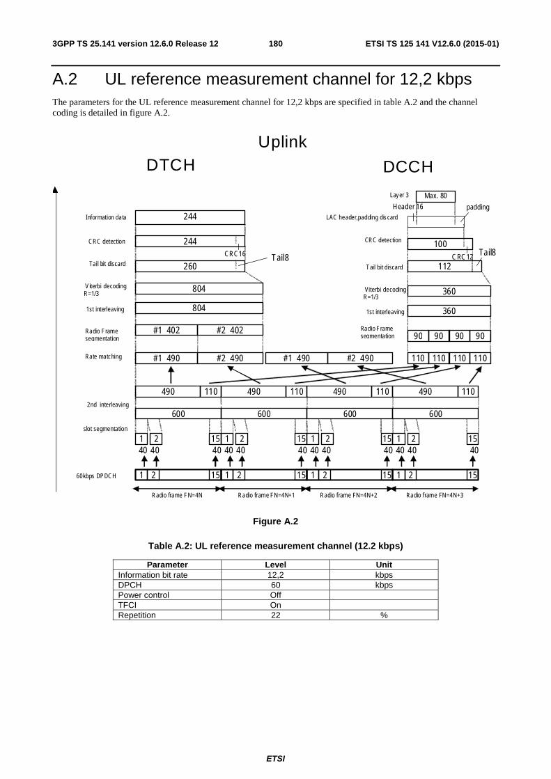
ETSI
ETSI TS 125 141 V12.6.0 (2015-01)1803GPP TS 25.141 version 12.6.0 Release 12
A.2 UL reference measurement channel for 12,2 kbps The parameters for the UL reference measurement channel for 12,2 kbps are specified in table A.2 and the channel coding is detailed in figure A.2.
DCCH
Uplink
DTCH
60kbps DPDCH
Viterbi decoding R=1/3
Radio frame FN=4N+1 Radio frame FN=4N+2 Radio frame FN=4N+3 Radio frame FN=4N
Information data
CRC detection
Tail bit discard
Rate matching
2nd interleaving
600
40 40 1
40
490 110
110
804
260 Tail8 CRC16
244
244
360
112
Tail8 100
Header 16
CRC12
padding Max. 80
1st interleaving
Radio Frame segmentation
slot segmentation
CRC detection
Layer 3
LAC header,padding discard
Tail bit discard
Viterbi decoding R=1/3
1st interleaving
#1 402 Radio Frame segmentation
804
#2 402
#2 490 #1 490 #2 490 #1 490
490 110 490 110 490 110
600 600 600
2 15
1 2 15
40 40 1
40 2 15
1 2 15
40 40 1
40 2 15
1 2 15
40 40 1
40 2 15
1 2 15
110 110 110
90 90 90 90
360
Figure A.2
Table A.2: UL reference measurement channel (12.2 kbps)
Parameter Level Unit Information bit rate 12,2 kbps DPCH 60 kbps Power control Off TFCI On Repetition 22 %

ETSI
ETSI TS 125 141 V12.6.0 (2015-01)1813GPP TS 25.141 version 12.6.0 Release 12
A.3 UL reference measurement channel for 64 kbps The parameters for the UL reference measurement channel for 64 kbps are specified in table A.3 and the channel coding is detailed in figure A.3.
DCCH
Uplink DTCH
240kbps DPDCH
Turbo Code R=1/3
1 2 15 • • • • 1 2 15 • • • • 1 2 15 • • • • 1 2 15 • • • •
Radio frame FN=4N+1 Radio frame FN=4N+2 Radio frame FN=4N+3 Radio frame FN=4N
Information data
CRC detection
Rate matching
2nd interleaving
2400
160 160 1 2 15
• • • • 1 2 15
• • • • 1 2 15
• • • • 1 2
160 15
• • • •
2293 107 2293 107
2293 107
2293
#1 2293 #2 2293 #3 2293 #4 2293 107 107 107 107
2400 2400 2400
7740
7740
2576 Termination 12
CRC16
2560
2560
107
360
360
112
Tail8 100
Header 16
CRC12
padding Max. 80
1st interleaving
Radio Frame segmentation
slot segmentation
CRC detection
Layer 3
LAC header,padding discard
Tail bit discard
Viterbi decoding R=1/3
1st interleving
#1 1935 #2 1935 #3 1935 #4 1935 90 90 90 90
Figure A.3
Table A.3: UL reference measurement channel (64kbps)
Parameter Level Unit Information bit rate 64 kbps DPCH 240 kbps Power control Off TFCI On Repetition 19 %

ETSI
ETSI TS 125 141 V12.6.0 (2015-01)1823GPP TS 25.141 version 12.6.0 Release 12
A.4 UL reference measurement channel for 144 kbps The parameters for the UL reference measurement channel for 144 kbps are specified in table A.4 and the channel coding is detailed in figure A.4.
DCCH
Uplink DTCH
480kbps DPDCH
Turbo Code R=1/3
1 2 15 • • • • 1 2 15 • • • • 1 2 15 • • • • 1 2 15 • • • •
Radio frame FN=4N+1 Radio frame FN=4N+2 Radio frame FN=4N+3 Radio frame FN=4N
Information data
CRC detection
Rate matching
2nd interleaving
4800
320 320 1 2 15
• • • • 1 2 15
• • • • 1 2 15
• • • • 1 2
320 15
• • • •
4702
98 4702 98
4702 98
4702
#1 4702 #2 4702 #3 4702 #4 4702 #1 98 #2 98 #3 98 #4 98
4800 4800 4800
17400
17400
5792 Termination 2x12
CRC16
2880
98
360
360
112
Tail8 100
Header 16
CRC12
padding Max. 80
1st interleaving
Radio Frame segmentation
slot segmentation
CRC detection
Layer 3
LAC header,padding discard
Tail bit discard
Viterbi decoding R=1/3
1 st interleaving
#1 4350 #2 4350 #3 4350 #4 4350 #1 90 #2 90 #3 90 #4 90
2880
2880 2880 CRC16
Figure A.4
Table A.4: UL reference measurement channel (144kbps)
Parameter Level Unit Information bit rate 144 kbps DPCH 480 kbps Power control Off TFCI On Repetition 8 %

ETSI
ETSI TS 125 141 V12.6.0 (2015-01)1833GPP TS 25.141 version 12.6.0 Release 12
A.5 UL reference measurement channel for 384 kbps The parameters for the UL reference measurement channel for 384 kbps are specified in table A.5 and the channel coding is detailed in figure A.5.
DCCH
Uplink DTCH
960kbps DPDCH
Turbo Code R=1/3
1 2 15 • • • • 1 2 15 • • • • 1 2 15 • • • • 1 2 15 • • • •
Radio frame FN=4N+1 Radio frame FN=4N+2 Radio frame FN=4N+3 Radio frame FN=4N
Information data
CRC detection
Rate matching
2nd interleaving
9600
640 640 1 2 15
• • • • 1 2 15
• • • • 1 2 15
• • • • 1 2
640 15
• • • •
9525
75 9525 75
9525 75
9525
#1 9525 #2 9525 #3 9525 #4 9525 #1 75 #2 75 #3 75 #4 75
9600 9600 9600
46320
46320
15424 Termination 4 x12
CRC16 15360
75
360
360
112
Tail8 100
Header 16
CRC12
padding Max. 80
1st interleaving
Radio Frame segmentation
slot segmentation
CRC detection
Layer 3
LAC header,padding discard
Tail bit discard
Viterbi decoding R=1/3
1st interleaving
#1 11580 #2 11580 #3 11580 #4 11580 #1 90 #2 90 #3 90 #4 90
3840 3840 3840 3840
3840 3840 3840 3840
Figure A.5
Table A.5: UL reference measurement channel (384kbps)
Parameter Level Unit Information bit rate 384 kbps DPCH 960 kbps Power control Off TFCI On Puncturing 18 %
A.6 (void) Figure A.6: (void)

ETSI
ETSI TS 125 141 V12.6.0 (2015-01)1843GPP TS 25.141 version 12.6.0 Release 12
Table A.6: (void)
A.7 Reference measurement channels for UL RACH The parameters for the UL RACH reference measurement channels are specified in Table A.7.
Table A.7: Reference measurement channels for UL RACH
Parameter Unit RACH CRC 16 bits
Channel Coding Rate ½ conv. coding TTI 20 ms TB size 168, 360 bits Rate Matching Repetition Number of diversity antennas
2
Preamble detection window size
256 chips
Ratio of preamble power and total message power (*)
0 dB
Power ratio of RACH Control/Data TB = 168
-2.69 dB
Power ratio of Control/Data TB = 360
-3.52 dB
NOTE *: If Power Offset Pp-m is used to adjust the power offset, Power Offset Pp-m shall be equal to -5 dB.
A.8 (void) Table A.8: (void)
A.9 Reference measurement channel for HS-DPCCH The parameters for the UL HS-DPCCH reference measurement channel are specified in Table A.9.

ETSI
ETSI TS 125 141 V12.6.0 (2015-01)1853GPP TS 25.141 version 12.6.0 Release 12
Table A.9: Reference measurement channel for HS-DPCCH
Parameter Unit
DPDCH
DTCH Information bit rate 12.2 kbps Physical channel 60 kbps Repetition rate 22 %
DCCH Information bit rate 2.4 kbps Physical channel 15 kbps Repetition rate 22 %
Spreading factor 64 Interleaving 20 ms Number of DPDCHs 1
DPCCH
Dedicated pilot 6 Bits/slot Power control 2 Bits/slot TFCI 2 Bits/slot Spreading factor 256
Power ratio of DPCCH/DPDCH -2.69 dB Amplitude ratio of DPCCH/DPDCH 0.7333 Closed loop power control OFF Repetition factor of ACK/NACK 1 HS-DPCCH power offset to DPCCH 0 dB HS-DPCCH timing offset to DPCCH 0 symbol
DPDCH/DPCCH are same as 12.2kbps reference measurement channel specified in Annex A.2.
A.9A Reference measurement channel for 4C-HSDPA HS-DPCCH
The parameters for the 4C-HSDPA UL HS-DPCCH reference measurement channel are specified in Table A.9A.
For RRC configuration, 0 dB shall be used for HS-DPCCH power offset to DPCCH in the test. In the reference measurement channels, HS-DPCCH power offset to DPCCH in Table A.9A shall be used for the waveform during the test as per the rule in Table 2b in Section 5.1.2.5A in TS 25.214 [13].

ETSI
ETSI TS 125 141 V12.6.0 (2015-01)1863GPP TS 25.141 version 12.6.0 Release 12
Table A.9A: Reference measurement channels for 4C-HSDPA HS-DPCCH
Parameter
Unit Carrier Configuration 4/4/4 4/4/2
3/3/3
3/2/1
3/3/0
DPDCH
DTCH Information bit rate 12.2 kbps Physical channel 60 kbps Repetition rate 22 %
DCCH Information bit rate 2.4 kbps Physical channel 15 kbps Repetition rate 22 %
Spreading factor 64 Interleaving 20 Ms Number of DPDCHs 1
DPCCH
Dedicated pilot 6 bits/slot Power control 2 bits/slot TFCI 2 bits/slot Spreading factor 256
Power ratio of DPCCH/DPDCH -2.69 dB Amplitude ratio of DPCCH/DPDCH 0.7333 Closed loop power control OFF HS-DPCCH repetition 1 HS-DPCCH power offset to DPCCH 4.08 2.05 4.08 2.05 2.05 dB HS-DPCCH timing offset to DPCCH 0 Symbol HS-DPCCH spreading factor 128 128 128 128 256 Secondary_Cell_Enabled 3 3 2 2 2 Secondary_Cell_Active 3 1 2 1 2 Number of MIMO carriers 4 2 3 1 0
Codebook
Rel10 DC-MIMO
codebook
Rel10 DC-MIMO
codebook repeated
Rel10 DC-MIMO
codebook
Rel10 DC-MIMO
codebook repeated
Rel10 TC-MIMO
codebook
Notes 2 Notes 3 Note 3 Note 1: Carrier configuration X/Y/Z denotes X number of carriers configured, Y number of active carriers, and Z
number of carriers configured as MIMO out of Y carriers. However, the configuration during the test follows Table 8.17C in TS 25.104.
Note 2: If the NodeB is not capable of MIMO on all 4 active carriers, the maximum supportable number of MIMO carriers is configured.
Note 3: Optional: Applies only if the NodeB is not capable of simultaneous 4 carrier operation.
A.10 Summary of E-DPDCH Fixed reference channels Table A.10.
Fixed Ref Channel TTI [ms] NINF SF1 SF2 SF3 SF4 NBIN Coding rate Max inf bit rate [kbps]
FRC1 2 2706 4 4 0 0 3840 0.705 1353.0 FRC2 2 5412 2 2 0 0 7680 0.705 2706.0 FRC3 2 8100 2 2 4 4 11520 0.703 4050.0 FRC4 10 5076 4 0 0 0 9600 0.529 507.6 FRC5 10 9780 4 4 0 0 19200 0.509 978.0 FRC6 10 19278 2 2 0 0 38400 0.502 1927.8 FRC7 10 690 16 0 0 0 2400 0.288 69.0 FRC8 2 16218 2 2 4 4 23040 0.704 8109.0 FRC9 2 16200 2 2 4 4 23040 0.703 8100.0
FRC10 2 32436 2 2 4 4 46080 0.704 16218.0

ETSI
ETSI TS 125 141 V12.6.0 (2015-01)1873GPP TS 25.141 version 12.6.0 Release 12
A.11 E-DPDCH Fixed reference channel 1 (FRC1) Table A.11
Parameter Unit Value Maximum. Inf. Bit Rate kbps 1353.0 TTI ms 2 Number of HARQ Processes Processes 8 Information Bit Payload (NINF) Bits 2706 Binary Channel Bits per TTI (NBIN) (3840 / SF x TTI sum for all channels)
Bits 3840
Coding Rate (NINF/ NBIN) 0.705 Physical Channel Codes SF for each
physical channel {4,4}
E-DPDCH testing: E-DPDCH/DPCCH power ratio E-DPCCH/DPCCH power ratio
dB dB dB dB
Diversity: 8.94 Non-diversity: 12.04 Diversity: 2.05 Non-diversity: 6.02 E-DPDCH /DPCCH power ratio is calculated for a single E-DPDCH.
E-DPCCH missed detection testing: E-DPDCH/DPCCH power ratio E-DPCCH/DPCCH power ratio
dB dB dB dB
Diversity: 8.94 Non-diversity: 12.04 Diversity: -1.94 Non-diversity: 0.00
Information Bit Payload NINF = 2706
CRC Addition
3 x (NINF+24) = 8190
Code Block Segmentation 2706+24 = 2730
Turbo Encoding (R=1/3)
RV Selection 3840
Physical Channel Segmentation 1920
24 NINF = 2706
12
1920
Figure A.11
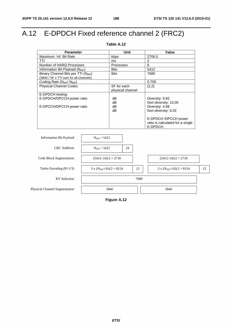
ETSI
ETSI TS 125 141 V12.6.0 (2015-01)1883GPP TS 25.141 version 12.6.0 Release 12
A.12 E-DPDCH Fixed reference channel 2 (FRC2) Table A.12
Parameter Unit Value Maximum. Inf. Bit Rate kbps 2706.0 TTI ms 2 Number of HARQ Processes Processes 8 Information Bit Payload (NINF) Bits 5412 Binary Channel Bits per TTI (NBIN) (3840 / SF x TTI sum for all channels)
Bits 7680
Coding Rate (NINF/ NBIN) 0.705 Physical Channel Codes SF for each
physical channel {2,2}
E-DPDCH testing: E-DPDCH/DPCCH power ratio E-DPCCH/DPCCH power ratio
dB dB dB dB
Diversity: 9.92 Non-diversity: 13.00 Diversity: 4.08 Non-diversity: 6.02 E-DPDCH /DPCCH power ratio is calculated for a single E-DPDCH.
Information Bit Payload NINF = 5412
CRC Addition
3 x (NINF+24)/2 = 8154
Code Block Segmentation (5412+24)/2 = 2718
Turbo Encoding (R=1/3)
RV Selection 7680
Physical Channel Segmentation 3840
24 NINF = 5412
12
(5412+24)/2 = 2718
3840
3 x (NINF+24)/2 = 8154 12
Figure A.12

ETSI
ETSI TS 125 141 V12.6.0 (2015-01)1893GPP TS 25.141 version 12.6.0 Release 12
A.13 E-DPDCH Fixed reference channel 3 (FRC3) Table A.13
Parameter Unit Value Maximum. Inf. Bit Rate kbps 4050.0 TTI ms 2 Number of HARQ Processes Processes 8 Information Bit Payload (NINF) Bits 8100 Binary Channel Bits per TTI (NBIN) (3840 / SF x TTI sum for all channels)
Bits 11520
Coding Rate (NINF/ NBIN) 0.703 Physical Channel Codes SF for each
physical channel {2,2,4,4}
E-DPDCH testing: E-DPDCH/DPCCH power ratio E-DPCCH/DPCCH power ratio
dB dB dB dB
Diversity: 6.02 Non-diversity: 8.94 Diversity: 0.0 Non-diversity: 2.05 E-DPDCH/DPCCH power ratio is calculated for a single E-DPDCH with SF 4. The power of an E-DPDCH with SF2 is twice that of an E-DPDCH with SF4.
Information Bit Payload NINF = 8100
CRC Addition
3 x (NINF+24)/2 = 12186
Code Block Segmentation (8100+24)/2 = 4062
Turbo Encoding (R=1/3)
RV Selection 11520
Physical Channel Segmentation 3840
24 NINF = 8100
12
(8100+24)/2 = 4062
3840 1920 1920
3 x (NINF+24)/2 = 12186 12
Figure A.13

ETSI
ETSI TS 125 141 V12.6.0 (2015-01)1903GPP TS 25.141 version 12.6.0 Release 12
A.14 E-DPDCH Fixed reference channel 4 (FRC4) Table A.14
Parameter Unit Value Maximum. Inf. Bit Rate kbps 507.6 TTI ms 10 Number of HARQ Processes Processes 4 Information Bit Payload (NINF) Bits 5076 Binary Channel Bits per TTI (NBIN) (3840 / SF x TTI sum for all channels)
Bits 9600
Coding Rate (NINF/ NBIN) 0.529 Physical Channel Codes SF for each
physical channel {4}
E-DPDCH testing: E-DPDCH/DPCCH power ratio E-DPCCH/DPCCH power ratio
dB dB dB dB
Diversity: 8.94 Non-diversity: 12.04 Diversity: -1.94 Non-diversity: 0.0
E-DPCCH missed detection testing: E-DPDCH/DPCCH power ratio E-DPCCH/DPCCH power ratio
dB dB dB dB
Diversity: 8.94 Non-diversity: 12.04 Diversity: -7.96 Non-diversity: -5.46
Information Bit Payload NINF = 5076
CRC Addition
3 x (NINF+24) = 15300
Code Block Segmentation 5076+24 = 5100
Turbo Encoding (R=1/3)
RV Selection 9600
Physical Channel Segmentation 9600
24 NINF = 5076
12
Figure A.14
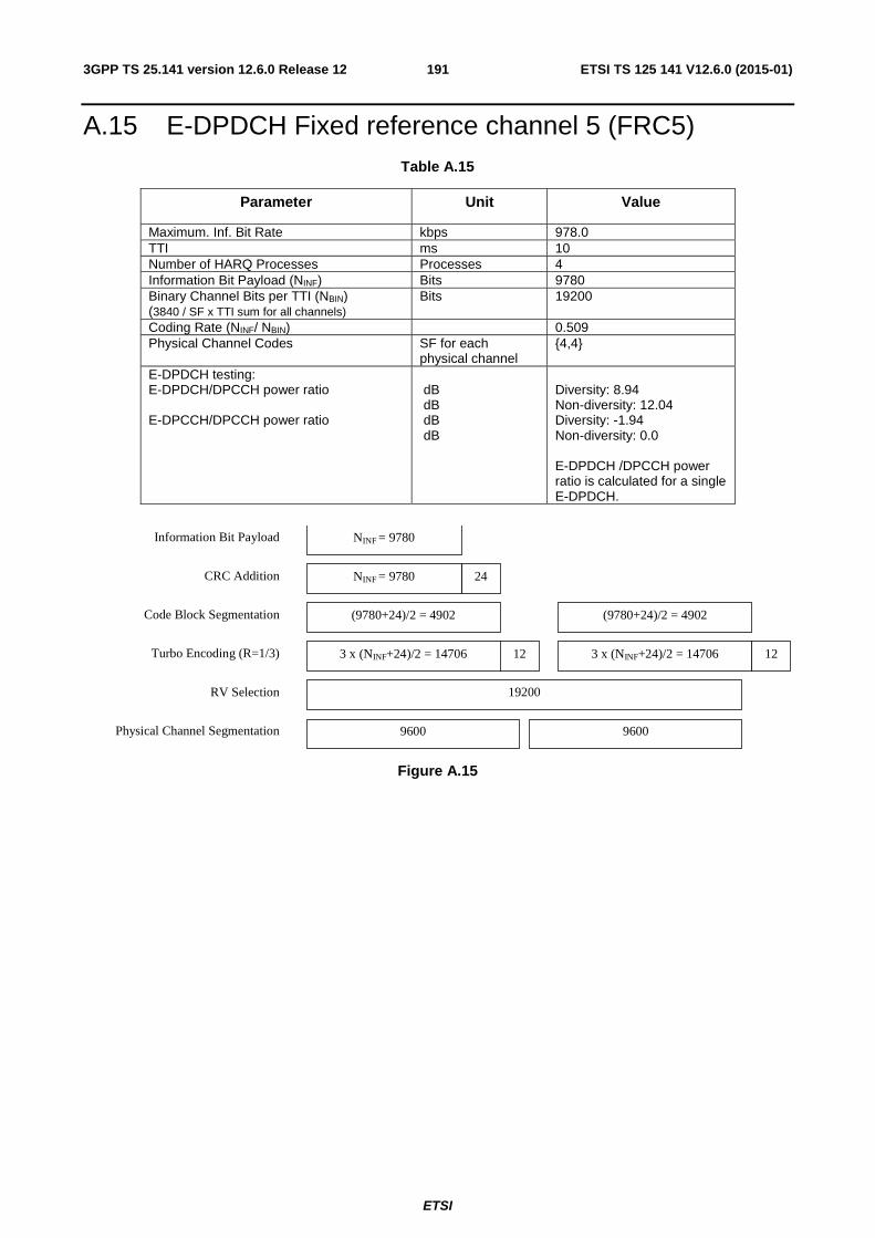
ETSI
ETSI TS 125 141 V12.6.0 (2015-01)1913GPP TS 25.141 version 12.6.0 Release 12
A.15 E-DPDCH Fixed reference channel 5 (FRC5) Table A.15
Parameter Unit Value
Maximum. Inf. Bit Rate kbps 978.0 TTI ms 10 Number of HARQ Processes Processes 4 Information Bit Payload (NINF) Bits 9780 Binary Channel Bits per TTI (NBIN) (3840 / SF x TTI sum for all channels)
Bits 19200
Coding Rate (NINF/ NBIN) 0.509 Physical Channel Codes SF for each
physical channel {4,4}
E-DPDCH testing: E-DPDCH/DPCCH power ratio E-DPCCH/DPCCH power ratio
dB dB dB dB
Diversity: 8.94 Non-diversity: 12.04 Diversity: -1.94 Non-diversity: 0.0 E-DPDCH /DPCCH power ratio is calculated for a single E-DPDCH.
Information Bit Payload NINF = 9780
CRC Addition
3 x (NINF+24)/2 = 14706
Code Block Segmentation (9780+24)/2 = 4902
Turbo Encoding (R=1/3)
RV Selection 19200
Physical Channel Segmentation 9600
24 NINF = 9780
12
(9780+24)/2 = 4902
9600
3 x (NINF+24)/2 = 14706 12
Figure A.15

ETSI
ETSI TS 125 141 V12.6.0 (2015-01)1923GPP TS 25.141 version 12.6.0 Release 12
A.16 E-DPDCH Fixed reference channel 6 (FRC6) Table A.16
Parameter Unit Value Maximum. Inf. Bit Rate kbps 1927.8 TTI ms 10 Number of HARQ Processes Processes 4 Information Bit Payload (NINF) Bits 19278 Binary Channel Bits per TTI (NBIN) (3840 / SF x TTI sum for all channels)
Bits 38400
Coding Rate (NINF/ NBIN) 0.502 Physical Channel Codes SF for each
physical channel {2,2}
E-DPDCH testing: E-DPDCH/DPCCH power ratio E-DPCCH/DPCCH power ratio
dB dB dB dB
Diversity: 9.92 Non-diversity: 13.00 Diversity: -5.46 Non-diversity: -1.94 E-DPDCH /DPCCH power ratio is calculated for a single E-DPDCH.
Information Bit Payload NINF = 19278
CRC Addition
Code Block Segmentation (19278+24)/4 = 4826
Turbo Encoding (R=1/3)
RV Selection 38400
Physical Channel Segmentation 19200
24 NINF = 19278
12
(19278+24)/4 = 4826 (19278+24)/4 = 4826 (19278+24)/4 = 4826
3 x 4826=14478 12 3 x 4826=14478
12 3 x 4826=14478
12 3 x 4826=14478
19200
Figure A.16
A.17 E-DPDCH Fixed reference channel 7 (FRC7) Table A.17
Parameter Unit Value Maximum. Inf. Bit Rate kbps 69.0 TTI ms 10 Number of HARQ Processes Processes 4 Information Bit Payload (NINF) Bits 690 Binary Channel Bits per TTI (NBIN) (3840 / SF x TTI sum for all channels)
Bits 2400
Coding Rate (NINF/ NBIN) 0.288 Physical Channel Codes SF for each
physical channel {16}
E-DPDCH testing: E-DPDCH/DPCCH power ratio E-DPCCH/DPCCH power ratio
dB dB dB dB
Diversity: 6.02 Non-diversity: 8.94 Diversity: 0.0 Non-diversity: 4.08
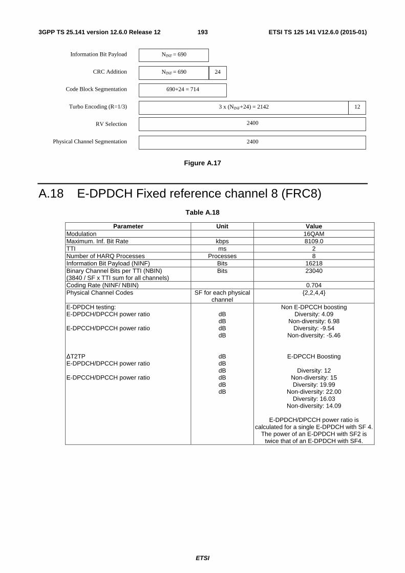
ETSI
ETSI TS 125 141 V12.6.0 (2015-01)1933GPP TS 25.141 version 12.6.0 Release 12
Information Bit Payload NINF = 690
CRC Addition
3 x (NINF+24) = 2142
Code Block Segmentation 690+24 = 714
Turbo Encoding (R=1/3)
RV Selection 2400
Physical Channel Segmentation 2400
24 NINF = 690
12
Figure A.17
A.18 E-DPDCH Fixed reference channel 8 (FRC8) Table A.18
Parameter Unit Value Modulation 16QAM Maximum. Inf. Bit Rate kbps 8109.0 TTI ms 2 Number of HARQ Processes Processes 8 Information Bit Payload (NINF) Bits 16218 Binary Channel Bits per TTI (NBIN) (3840 / SF x TTI sum for all channels)
Bits 23040
Coding Rate (NINF/ NBIN) 0.704 Physical Channel Codes SF for each physical
channel {2,2,4,4}
E-DPDCH testing: E-DPDCH/DPCCH power ratio E-DPCCH/DPCCH power ratio ∆T2TP E-DPDCH/DPCCH power ratio E-DPCCH/DPCCH power ratio
dB dB dB dB
dB dB dB dB dB dB
Non E-DPCCH boosting Diversity: 4.09
Non-diversity: 6.98 Diversity: -9.54
Non-diversity: -5.46
E-DPCCH Boosting
Diversity: 12 Non-diversity: 15 Diversity: 19.99
Non-diversity: 22.00 Diversity: 16.03
Non-diversity: 14.09
E-DPDCH/DPCCH power ratio is calculated for a single E-DPDCH with SF 4.
The power of an E-DPDCH with SF2 is twice that of an E-DPDCH with SF4.

ETSI
ETSI TS 125 141 V12.6.0 (2015-01)1943GPP TS 25.141 version 12.6.0 Release 12
Information Bit Payload
CRC Addition
Code Block Segmentation
Turbo Encoding (R=1/3)
RV Selection 23040
Physical Channel Segmentation 7680 7680
3840 3840
NINF = 16218
NINF = 16218
(16218+24)/4 = 4061 (16218+24)/4 = 4061 (16218+24)/4 = 4061 (16218+24)/4 = 4061
12 3 x 4061=12183 12 3 x 4061=12183 12 3 x 4061=12183 12 3 x 4061=12183
Figure A.18
A.19 E-DPDCH Fixed reference channel 9 (FRC9) Table A.19
Parameter Unit Value
Modulation QPSK
Maximum. Inf. Bit Rate kbps 8100
TTI ms 2
Number of HARQ Processes Processes 8
Information Bit Payload (NINF) Bits 16200
Binary Channel Bits per TTI (NBIN) (3840 / SF x TTI sum for all channels)
Bits 23040
Coding Rate (NINF/ NBIN) 0.703
Physical Channel Codes SF for each physical channel
{2,2,4,4}
E-DPDCH/DPCCH power ratio E-DPCCH/DPCCH power ratio S-DPCCH/DPCCH power ratio S-E-DPCCH/DPCCH power ratio S-E-DPDCH/DPCCH power ratio
dB dB dB dB dB
6.02 -1.94 -1.94 0.00 6.02 E-DPDCH/DPCCH power ratio is calculated for a single E-DPDCH with SF 4. The power of an E-DPDCH with SF2 is twice that of an E-DPDCH with SF4.

ETSI
ETSI TS 125 141 V12.6.0 (2015-01)1953GPP TS 25.141 version 12.6.0 Release 12
Information Bit Payload NINF = 8100
CRC Addition
3 x (NINF+24)/2 = 12186
Code Block Segmentation (8100+24)/2 = 4062
Turbo Encoding (R=1/3)
RV Selection 11520
Physical Channel Segmentation 3840
24 NINF = 8100
12
(8100+24)/2 = 4062
3840 1920 1920
3 x (NINF+24)/2 = 12186 12
Figure A.19 E-DPDCH
Information Bit Payload NINF = 8100
CRC Addition
3 x (NINF+24)/2 = 12186
Code Block Segmentation (8100+24)/2 = 4062
Turbo Encoding (R=1/3)
RV Selection 11520
Physical Channel Segmentation 3840
24 NINF = 8100
12
(8100+24)/2 = 4062
3840 1920 1920
3 x (NINF+24)/2 = 12186 12
Figure A.19A S-E-DPDCH

ETSI
ETSI TS 125 141 V12.6.0 (2015-01)1963GPP TS 25.141 version 12.6.0 Release 12
A.20 E-DPDCH Fixed reference channel 10 (FRC10) Table A.20
Parameter Unit Value
Modulation 16QAM
Maximum. Inf. Bit Rate kbps 16218
TTI ms 2
Number of HARQ Processes Processes 8
Information Bit Payload (NINF) Bits 32436
Binary Channel Bits per TTI (NBIN) (3840 / SF x TTI sum for all channels)
Bits 46080
Coding Rate (NINF/ NBIN) 0.704
Physical Channel Codes SF for each physical channel
{2,2,4,4}
E-DPDCH/DPCCH power ratio E-DPCCH/DPCCH power ratio S-DPCCH/DPCCH power ratio S-E-DPCCH/DPCCH power ratio S-E-DPDCH/DPCCH power ratio
dB dB dB dB dB
19.99 16.03 16.03 6.02 19.99 E-DPDCH/DPCCH power ratio is calculated for a single E-DPDCH with SF 4. The power of an E-DPDCH with SF2 is twice that of an E-DPDCH with SF4.
Information Bit Payload
CRC Addition
Code Block Segmentation
Turbo Encoding (R=1/3)
RV Selection 23040
Physical Channel Segmentation 7680 7680
3840 3840
NINF = 16218
NINF = 16218
(16218+24)/4 = 4061 (16218+24)/4 = 4061 (16218+24)/4 = 4061 (16218+24)/4 = 4061
12 3 x 4061=12183 12 3 x 4061=12183 12 3 x 4061=12183 12 3 x 4061=12183
Figure A.20 E-DPDCH
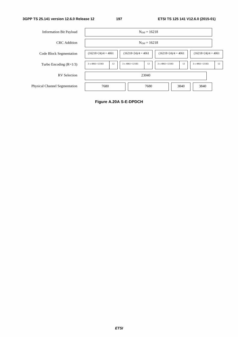
ETSI
ETSI TS 125 141 V12.6.0 (2015-01)1973GPP TS 25.141 version 12.6.0 Release 12
Information Bit Payload
CRC Addition
Code Block Segmentation
Turbo Encoding (R=1/3)
RV Selection 23040
Physical Channel Segmentation 7680 7680
3840 3840
NINF = 16218
NINF = 16218
(16218+24)/4 = 4061 (16218+24)/4 = 4061 (16218+24)/4 = 4061 (16218+24)/4 = 4061
12 3 x 4061=12183 12 3 x 4061=12183 12 3 x 4061=12183 12 3 x 4061=12183
Figure A.20A S-E-DPDCH

ETSI
ETSI TS 125 141 V12.6.0 (2015-01)1983GPP TS 25.141 version 12.6.0 Release 12
Annex B (informative): Measurement system set-up Example of measurement system set-ups are attached below as an informative annex.
B.1 Transmitter
B.1.1 Maximum output power, total power dynamic range
Power meter or equivalent
BS under test
Figure B.1: Measuring system Set-up for maximum output power, total power dynamic range
B.1.2 Frequency, Code Power and Transmit Modulation
Measurement equipment (Global in-Channel TX tester)
BS under test
Figure B.2: Measurement system set up for RF frequency, several code power tests and transmit modulation (EVM, RCDE and PCDE)
Figure B.2A: Measurement system set-up for S-CPICH power offset accuracy. For MIMO mode with two antennas the components surrounded by the dashed line do not exist.

ETSI
ETSI TS 125 141 V12.6.0 (2015-01)1993GPP TS 25.141 version 12.6.0 Release 12
B.1.3 Power control steps and power control dynamic range
UL signal generator
(Psudo UE)
Base Station
Under Test
Attenuator
Code domain
analyser
Rx
Tx
Figure B.3: Measuring system Set-up for power control steps and power control dynamic range measurements
B.1.4 Out of band emission
Measurement
device
BS
under test
Figure B.4: Measuring system Set-up for Out of band emission measurements
B.1.5 Transmit intermodulation
Base station
Under test
RX/TX or
TX
Spectrum analyser
Signal Generator
for the WCDMA
ATT1modulated
Figure B.5: Measuring system Set-up for Base Station Transmit Intermodulation Tests

ETSI
ETSI TS 125 141 V12.6.0 (2015-01)2003GPP TS 25.141 version 12.6.0 Release 12
B.1.6 Time alignment error in TX diversity, MIMO, DC-HSDPA, DB-DC-HSDPA and 4C-HSDPA
Timing analyzer
BS under Tx test
Tx 1
Tx 2
Figure B.6: Measuring system set-up for time alignment error in TX diversity, MIMO, DC-HSDPA and DB-DC-HSDPA transmission (one of Tx1 or Tx2 may not be used for DC-HSDPA or 4C-HSDPA)
B.1.7 Home BS output power for adjacent channel protection
Home BS (DUT) Signal generator for
co-channel interference
Signal generator for adjacent channel
DL signal ATT1
ATT2
HYB
2
1 D
Power meter
a*
b*
c*
* antenna ports - a (optional): DL measurement receiver connector - b: main antenna port (UL/DL) - c (optional): diversity antenna port
Figure B.7: Measuring system set-up for Home BS output power for adjacent channel protection

ETSI
ETSI TS 125 141 V12.6.0 (2015-01)2013GPP TS 25.141 version 12.6.0 Release 12
B.2 Receiver
B.2.1 Reference sensitivity level
BS
RXA orRXA/TX
RXB
BER (optional)
BER
(if needed)
RF signal source or UE simulator RF out
Termination (if needed)
Figure B.7: Measuring system Set-up for Base Station Reference sensitivity level Testes
B.2.2 Dynamic range
Signal generator for the wanted signal
Signal generator for the AWGN interfering signal
Hybrid
Base station under test RX1 RX2 BER measure (optional)
BER Measure
(if needed)
Termination (if needed)
Figure B.8: Measuring system Set-up for Dynamic range

ETSI
ETSI TS 125 141 V12.6.0 (2015-01)2023GPP TS 25.141 version 12.6.0 Release 12
B.2.3 Adjacent Channel Selectivity (ACS)
Base station
Under test
a)
a) RX1
RX2
(optional)
HYBRID
ATT2
ATT1Signal Generator
for the reference channel
Signal Generator
for the interferencesignal
BER measure
(if needed)
Termination (if needed)
BER measure
Figure B.9: Measuring system Set-up for Adjacent channel selectivity
B.2.4 Blocking characteristics
Mobil StationSimulatoror RFsource
RX
TX
ATT 1
Signal Generator
Under TestBase Station
T/RX1
RX2Desired Signal
Interference Signal
BER measure (if needed)
HYB HYBATT 2
ATT 3
BER measure(optional)
Figure B.10: Measuring system Set-up for Blocking characteristics

ETSI
ETSI TS 125 141 V12.6.0 (2015-01)2033GPP TS 25.141 version 12.6.0 Release 12
B.2.5 Intermodulation characteristics
HYBRID
ATT2
ATT1Signal Generator for the wanted
signal
Signal Generator for the CW
interference signal
Termination (if needed)
Signal Generator for the WCDMA
modulated interference signal
ATT3
HYBRID
Base station
Under test
a) RX1
RX2
BER measure(optional)
a) BER measure
Figure B.11: Measuring system Set-up for intermodulation characteristics
B.2.6 Receiver spurious emission
Measurement receiver
TX notch
BS
TX
RXB
Terminator
RXA
Figure B.12: Measuring system Set-up for Receiver spurious emission

ETSI
ETSI TS 125 141 V12.6.0 (2015-01)2043GPP TS 25.141 version 12.6.0 Release 12
B.3 Performance requirement
B.3.1 Demodulation of DCH, RACH and HS-DPCCH signalling in static conditions
RX A
RX B
Base Station
under test
BS tester
AWGN Generator
AWGN Generator
Figure B.13: Functional Set-up for Demodulation of DCH, RACH and HS-DPCCH in static conditions for BS with Rx diversity
RX
Base Station
under test
BS tester
AWGN Generator
Figure B.13A: Functional Set-up for Demodulation of DCH, RACH and HS-DPCCH in static conditions for BS without Rx diversity

ETSI
ETSI TS 125 141 V12.6.0 (2015-01)2053GPP TS 25.141 version 12.6.0 Release 12
B.3.2 Demodulation of DCH, RACH and HS-DPCCH signalling in multipath fading conditions
RX A
RX B
Base Station
under test BS
tester
ChannelSimulator
or ChannelSimulator
AWGN Generator
AWGN Generator
Figure B.14: Functional Set-up for Demodulation of DCH, RACH and HS-DPCCH in multipath fading conditions for BS with Rx diversity
RX
Base Station
under test
BS tester
AWGN Generator
Channel Simulator
Figure B.14A: Functional Set-up for Demodulation of DCH, RACH and HS-DPCCH in multi-path fading conditions for BS without Rx diversity
B.3.3 Verification of the internal BER and BLER calculation
BS tester
RX A
RX B
Base Station
under test
Figure B.15: Functional Set-up for Verification of the internal BLER calculation for BS with Rx diversity

ETSI
ETSI TS 125 141 V12.6.0 (2015-01)2063GPP TS 25.141 version 12.6.0 Release 12
BS tester RX
Base Station
under test
Figure B.15A: Functional Set-up for Verification of the internal BLER calculation for BS without Rx diversity
BS tester RX A
RX B
Base Station
under test
Figure B.16: Functional Set-up for Verification of the internal BER calculation
B.3.4 Demodulation of E-DPDCH, S-E-DPDCH and E-DPCCH signalling in multipath fading conditions
HARQ Feedback
BS tester
BS Station Under test
RX A RX B
AWGN Generator
AWGN Generator
Channel Simulator
Channel Simulator
NOTE: The HARQ feedback could be done as an RF feedback or as a digital feedback. The HARQ feedback should be error free.
Figure B.17: Functional Set-up for Demodulation of E-DPDCH and E-DPCCH in multipath fading conditions for BS with Rx diversity

ETSI
ETSI TS 125 141 V12.6.0 (2015-01)2073GPP TS 25.141 version 12.6.0 Release 12
HARQ Feedback
BS tester
BS Station Under test
RX A RX B
AWGN Generator
AWGN Generator
Channel Simulator
Channel Simulator
NOTE: The HARQ feedback could be done as an RF feedback or as a digital feedback. The HARQ feedback should be error free.
Figure B.17A: Functional Set-up for Demodulation of E-DPDCH and S-E-DPDCH in multipath fading conditions for UL MIMO
HARQ Feedback
BS tester
BS Station Under test
RX
AWGN Generator
Channel Simulator
NOTE: The HARQ feedback could be done as an RF feedback or as a digital feedback. The HARQ feedback should be error free.
Figure B.18: Functional Set-up for Demodulation of E-DPDCH and E-DPCCH in multipath fading conditions for BS without Rx diversity

ETSI
ETSI TS 125 141 V12.6.0 (2015-01)2083GPP TS 25.141 version 12.6.0 Release 12
B.3.5 Demodulation of DCH in moving propagation conditions or birth-death propagation conditions, or Demodulation of DCH, RACH in high speed train conditions
BS tester
BS Station Under test
RX A RX B
AWGN Generator
AWGN Generator
Channel Simulator
Figure B.19: Functional Set-up for Demodulation of DCH in moving propagation conditions or birth-death propagation conditions, or Demodulation of DCH, RACH in high speed train conditions for BS
with Rx diversity
RX
Base Station
under test
BS tester
AWGN Generator
Channel Simulator
Figure B.20: Functional Set-up for Demodulation of DCH in moving propagation conditions or birth-death propagation conditions, or Demodulation of DCH, RACH in high speed train conditions for BS
without Rx diversity

ETSI
ETSI TS 125 141 V12.6.0 (2015-01)2093GPP TS 25.141 version 12.6.0 Release 12
Annex C (normative): General rules for statistical testing
C.1 Statistical testing of receiver BER/BLER performance
C.1.1 Error Definition Bit Error Ration (BER) and Block Error Ratio (BLER) are defined in section 3.1.
C.1.2 Test Method Each test is performed in the following manner:
a) Setup the required test conditions.
b) Record the number of samples tested and the number of occurred events (bit error or block error)
c) Stop the test at a stop criterion which is minimum test time or an early pass or an early fail event.
d) Once the test is stopped decide according to the pass fail decision rules ( clause C.1.7)
C.1.3 Test Criteria The test shall fulfil the following requirements:
a) good pass fail decision
1) to keep reasonably low the probability (risk) of passing a bad unit for each individual test;
2) to have high probability of passing a good unit for each individual test;
b) good balance between test time and statistical significance
3) to perform measurements with a high degree of statistical significance;
4) to keep the test time as low as possible.
C.1.4 Calculation assumptions
C.1.4.1 Statistical independence
a) It is assumed, that error events are rare (lim BER BLER � 0) independent statistical events. However the memory of the convolutional /turbo coder is terminated after one TTI. Samples and errors are summed up every TTI. So the assumption of independent error events is justified.
b) In the BLER test with fading there is the memory of the multipath fading channel which interferes the statistical independence. A minimum test time is introduced to average fluctuations of the multipath fading channel. So the assumption of independent error events is justified approximately.
C.1.4.2 Applied formulas
The formulas, applied to describe the BER BLER test, are based on the following experiments:
1) After having observed a certain number of errors (ne) the number of samples are counted to calculate BER BLER. Provisions are made (note 1) such that the complementary experiment is valid as well:

ETSI
ETSI TS 125 141 V12.6.0 (2015-01)2103GPP TS 25.141 version 12.6.0 Release 12
2) After a certain number of samples (ns) the number of errors, occurred, are counted to calculate BER BLER.
Experiment 1) stipulates to use the following Chi Square Distribution with degree of freedom ne:
2*dchisq(2*NE,2*ne).
Experiment 2) stipulates to use the Poisson Distribution:
dpois(ne,NE)
(NE: mean of the distribution)
To determine the early stop conditions, the following inverse cumulative operation is applied:
0.5 * qchisq(D,2*ne). This is applicable for experiment (1) and (2).
D: wrong decision risk per test step
NOTE: Other inverse cumulative operations are available, however only this is suited for experiment (1) and (2).
C.1.4.3 Approximation of the distribution
The test procedure is as follows:
During a running measurement for a UE ns (number of samples) and ne (number of errors) are accumulated and from this the preliminary BER BLER is calculated. Then new samples up to the next error are taken. The entire past and the new samples are basis for the next preliminary BER BLER. Depending on the result at every step, the UE can pass, can fail or must continue the test.
As early pass- and early fail-UEs leave the statistical totality under consideration, the experimental conditions are changed every step resulting in a distribution that is truncated more and more towards the end of the entire test. Such a distribution can not any more be handled analytically. The unchanged distribution is used as an approximation to calculate the early fail and early pass bounds.
C.1.5 Definition of good pass fail decision. This is defined by the probability of wrong decision F at the end of the test. The probability of a correct decision is 1-F.
The probability (risk) to fail a good DUT shall be ≤ F according to the following definition: The failed DUT is still better than the specified error ratio (Test requirement)with a probability of ≤ F.
The probability to pass a bad DUT shall be ≤ F according to the following definition: The passed DUT is still worse than M times the specified error ratio (M>1 is the bad DUT factor) with a probability of ≤ F.
This definitions lead to an early pass and an early fail limit:
Early fail: ber≥ berlimfail
)*2,(
*2),(lim
neDqchisq
neneDber fail = (1)
For ne≥7
Early pass: ber ≤berlimbadpass
)*2,1(
**2),(lim
neDqchisq
MneneDbadber pass −
= (2)
For ne ≥ 1
With

ETSI
ETSI TS 125 141 V12.6.0 (2015-01)2113GPP TS 25.141 version 12.6.0 Release 12
ber (normalized BER,BLER): BER,BLER according to C.1.1 divided by Test requirement
D: wrong decision probability for a test step . This is a numerically evaluated fraction of F, the wrong decision probability at the end of the test. See table C.1.
ne: Number of error events
M: bad DUT factor see table C.1.
qchisq: inverse-cumulative-function of the chi-squared-distribution
C.1.6 Good balance between test time and statistical significance Three independent test parameters are introduced into the test and shown in Table C.1. These are the obvious basis of test time and statistical significance. From the first two of them four dependent test parameters are derived. The third independent test parameter is justified separately.
Table C.1: independent and dependent test parameters
Independent test parameters Dependent test parameters Test Parameter Value Reference Test parameter Value Reference
Bad DUT factor M 1.5 Tables C.3 to C.9 Early pass/fail condition
Curves Clause C.1.5 Figure C.1.9
Final probability of wrong pass/fail
decision F
0.2%, (0.02%, note 2)
Clause C.1.5 Target number of error events
345 Tables C.3 to C.9
Probability of wrong pass/fail
decision per test step D
0.0085%, (0.0008% and
0.008%, note 2)
Test limit factor TL 1.234 Tables C.3 to C.9 Minimum test time Table C.2
The minimum test time is derived from the following justification:
1) For no propagation conditions and static propagation condition
No early fail calculated from fractional number of errors <1 (see note 1)
2) For multipath fading condition
No stop of the test until 990 wavelengths are crossed with the speed given in the fading profile.
3) For birth death propagation conditions
No stop of the test until 200 birth death transitions occur
4) For moving propagation conditions: 628 sec
This is necessary in order to pass all potential critical points in the moving propagation profile 4 times: Maximum rake window, Maximum adjustment speed, Intersection of moving taps
5) For high speed train conditions
Scenario 1: 82.3s. This corresponds to 4 complete cycles of approach towards and departure leave to and from a BS antenna
Scenario 2: The test shall continue until 990 wavelengths are crossed with the speed given in the fading profile (1.8s corresponding 300 km/h)
Scenario 3: 28.8s. This corresponds to 4 complete cycles of approach towards and departure from a BS antenna

ETSI
ETSI TS 125 141 V12.6.0 (2015-01)2123GPP TS 25.141 version 12.6.0 Release 12
Table C.2: minimum Test time
Fading profile Minimum test time Multipath propagation Case 1, Case 2 164 sec Multipath propagation Case 3 4.1 sec Multipath propagation Case 4 2 sec Birth Death propagation 38.2 sec Moving propagation 628 sec High speed train conditions Scenario 1 82.3 sec High speed train conditions Scenario 2 1.8 sec High speed train conditions Scenario 3 28.8 sec
In table C.3 to C.9 the minimum test time is converted in minimum number of samples.
C.1.7 Pass fail decision rules No decision is allowed before the minimum test time is elapsed.
1) If minimum Test time < time for target number of error events then the following applies: The required confidence level 1-F (= correct decision probability) shall be achieved. This is fulfilled at an early pass or early fail event.
For BER:
For every TTI (Transmit Time Interval) sum up the number of bits (ns) and the number if errors (ne) from the beginning of the test and calculate
BER1 (including the artificial error at the beginning of the test (Note 1))and
BER0 (excluding the artificial error at the beginning of the test (Note 1)).
If BER0 is above the early fail limit, fail the DUT.
If BER1 is below the early pass limit, pass the DUT.
Otherwise continue the test
For BLER:
For every TTI sum up the number of blocks (ns) and the number of erroneous blocks (ne) from the beginning of the test and calculate
BLER1 (including the artificial error at the beginning of the test (Note 1))and
BLER0 (excluding the artificial error at the beginning of the test (Note 1)).
If BLER1 is below the early pass limit, pass the DUT.
If BLER0 is above the early fail limit, fail the DUT.
Otherwise continue the test
2) If the minimum test time ≥ time for target error events, then the test runs for the minimum test time and the decision is done by comparing the result with the test limit.
For BER:
For every TTI (Transmit Time Interval) sum up the number of bits (ns) and the number if errors (ne) from the beginning of the test and calculate BER0
For BLER:
For every TTI sum up the number of blocks (ns) and the number of erroneous blocks (ne) from the beginning of the test and calculate BLER0
If BER0/BLER0 is above the test limit, fail the DUT.

ETSI
ETSI TS 125 141 V12.6.0 (2015-01)2133GPP TS 25.141 version 12.6.0 Release 12
If BER0/BLER0 is on or below the test limit, pass the DUT.
C.1.8 Test conditions for BER, BLER, Pd, E-DPCCH tests
Table C.3: Test conditions for BER tests
Type of test (BER)
Propagation conditions
Test requirement
(BER)
Test limit (BER)= Test requirement (BER)x TL
TL
Target number of error events
(time)
Minimum number
of samples
Prob that good unit
will fail = Prob that
bad unit will pass
(%)
Bad unit BER factor
M
Reference Sensitivity Level
- 0.001 1.234 345 (22.9s) Note 1 0.2 1.5
Dynamic Range - 0.001 1.234 345 (22.9s) Note 1 0.2 1.5 Adjacent Channel
Selectivity - 0.001 1.234 345 (22.9s) Note 1 0.2 1.5
Blocking Characteristics Pass condition
Note 2
- 0.001 1.251 402 (26.3s) Note 1 0.2 1.5
Blocking Characteristics Fail condition
Note 2
- 0.001 1.251 402 (26.3s) Note 1 0.02 1.5
Intermodulation Characteristics
- 0.001 1.234 345 (22.9s) Note 1 0.2 1.5
Verification of internal BER calculation
Not applicable, TS 34.121 Annex F.6.1.10 Dual limit BLER Tests may be applied in principle

ETSI
ETSI TS 125 141 V12.6.0 (2015-01)2143GPP TS 25.141 version 12.6.0 Release 12
Table C.4: Test conditions for BLER tests
Type of test (BLER)
Information Bit rate
Test requirement
(BLER)
Test limit (BLER)=
Test requirement (BLER)x TL
TL
Target number of
error events (time)
Minimum number of samples
(time)
Prob that bad unit will
pass = Prob that good unit
will fail (%)
Bad unit BLER factor
M
Demodulation in Static Propagation
conditions
12.2 64
144
384
0.01 0.1
0.01 0.1
0.01 0.1
0.01
1.234 345 (559s) (112s) (1118s) (55.9s) (559s) (28s)
(280s)
Note 1 0.2 1.5
Demodulation of DCH in Multi-path
Fading Propagation conditions
(Case 1, Case 2)
12.2 64
144
384
0.01 0.1
0.01 0.1
0.01 0.1
0.01
1.234 345 (559s) (112s) (1118s) (55.9s) (559s) (28s)
(280s)
(164s) 8200 4100 4100 8200 8200
16400 16400
0.2 1.5
Demodulation of DCH in Multi-path
Fading Propagation conditions (Case3)
12.2
64
144
384
0.01
0.001 0.1
0.01 0.001
0.1 0.01
0.001 0.1
0.01 0.001
1.234 345 (559s) (5592s) (112s) (1118s)
(11183s) (55.9s) (559s) (5592s) (28s)
(280s) (2796s)
(4.1s) 205 205 103 103 103 205 205 205 410 410 410
0.2 1.5
Demodulation of DCH in Multi-path
Fading Propagation conditions (Case 4)
12.2
64
144
384
0.01
0.001 0.1
0.01 0.001
0.1 0.01
0.001 0.1
0.01 0.001
1.234 345 (559s) (5592s) (112s) (1118s)
(11183s) (55.9s) (559s) (5592s) (28s)
(280s) (2796s)
(2s) 100 100 50 50 50
100 100 100 200 200 200
0.2 1.5
Demodulation of DCH in moving
propagation conditions
12.2 64
0.01 0.1
0.01
1.234 345 (559s) (112s) (1118s)
(628s) 31400 15700 15700
0.2
1.5
Demodulation of DCH in birth/death
propagation conditions
12.2 64
0.01 0.1
0.01
1.234 345 (559s) (112s) (1118s)
(38.2s) 1910 955 955
0.2 1.5
Demodulation of DCH in high speed
train conditions
12.2
0.01
1.234 345 (559s)
Scenario 1 (82.3s) 4115
Scenario 2 (1.8s)
90 Scenario 3
(28.8s) 1440
0.2 1.5
Verification of internal BLER
calculation
Not applicable, TS 34.121 Annex F.6.1.10 Dual limit BLER Tests may be applied in principle

ETSI
ETSI TS 125 141 V12.6.0 (2015-01)2153GPP TS 25.141 version 12.6.0 Release 12
Table C.5: Test conditions for Pd tests (Probability of detection)
Type of test Information Bit rate
Not
applicable
Test requirement
(1-Pd)
Test limit (1-Pd)= Test
requirement (1-Pd)x TL
TL
Target number of
error events (time)
Minimum number of samples
(time)
Prob that bad unit will pass = Prob that
good unit will fail (%)
Bad unit BLER
factor M
RACH preamble detection in static
propagation conditions
0.01
0.001
1.234 345 (29.8s) (298s) (net
preamble TX time)
Note 1 0.2 1.5
RACH preamble detection in multipath
fading conditions (case3)
0.01
0.001
1.234 345 (29.8s) (298s) (net
preamble TX time)
3844
preambles (4.1s)
0.2 1.5
RACH preamble detection in high speed
train conditions
0.01
0.001
1.234 345 (29.8s) (298s) (net
preamble TX time)
Scenario 1 77157
preambles (82.3s)
Scenario 2 1688
preambles (1.8s)
Scenario 3 27000
preambles (28.8s)
0.2 1.5

ETSI
ETSI TS 125 141 V12.6.0 (2015-01)2163GPP TS 25.141 version 12.6.0 Release 12
Table C.6: Test conditions for BLER tests
Type of test (BLER)
Information Bits
Test requirement
(BLER)
Test limit (BLER)= Test requirement (BLER)x TL
TL
Target number of
error events (time)
Minimum number of samples
(time)
Prob that bad unit will pass = Prob that
good unit will fail (%)
Bad unit BLER
factor M
Demodulation of RACH message in static propagation
conditions
168 bits
360 bits
0.1
0.01 0.1
0.01
1.234 345 (55.9s) (559s) (55.9s) (559s) (net
message TX time)
Note 1 0.2 1.5
Demodulation of RACH message in
multipath fading case 3
168 bits
360 bits
0.1
0.01 0.1
0.01
1.234 345 55.9s) (559s) (55.9s) (559s) (net
message TX time)
205 messages
(4.1s)
0.2 1.5
Demodulation of RACH message in
high speed train conditions
168 bits
360 bits
0.1
0.01 0.1
0.01
1.234 345 (55.9s) (559s) (55.9s) (559s) (net
message TX time)
Scenario 1 4115
messages (82.3s)
Scenario 2 90 messages
(1.8s) Scenario 3
1440 messages
(28.8s)
0.2 1.5

ETSI
ETSI TS 125 141 V12.6.0 (2015-01)2173GPP TS 25.141 version 12.6.0 Release 12
Table C.7: (void)
Table C.8: (void)
Table C.9: Test conditions for Error ratio tests
Type of test Information Bit rate
(Not applicable)
Test requirement error ratio
Test limit (error ratio)
= Test requirement (error rate) x
TL TL
Target number of
error events (time)
Minimum number of samples
(time)
Prob that bad unit will
pass = Prob that good unit
will fail (%)
Bad unit Error ratio factor M
ACK false alarm in static propagation
conditions
0.01 1.234 345 (18.6s)
(net ACK/NACK
TX time)
Note 1 0.2 1.5
ACK false alarm in multipath fading
conditions (Case 1, Case 2)
0.01 1.234 345 (18.6s)
(net ACK/NACK
TX time)
(164s) 246000
ACK/NAK slots
0.2 1.5
ACK false alarm in multipath fading
conditions (Case 3)
0.01 1.234 345 (18.6s)
(net ACK/NACK
TX time)
(4.1s) 6150
ACK/NAK slots
0.2 1.5
ACK mis-detection in static propagation
conditions
0.01 1.234 345 (18.6s)
(net ACK/NACK
TX time)
Note 1 0.2 1.5
ACK mis-detection in multipath fading
conditions (Case 1, Case 2)
0.01 1.234 345 (18.6s)
(net ACK/NACK
TX time)
(164s) 246000
ACK/NAK slots
0.2 1.5
ACK mis-detection in multipath fading
conditions (Case 3)
0.01 1.234 345 (18.6s)
(net ACK/NACK
TX time)
(4.1s) 6150
ACK/NAK slots
0.2 1.5

ETSI
ETSI TS 125 141 V12.6.0 (2015-01)2183GPP TS 25.141 version 12.6.0 Release 12
Table C.10: Test conditions E-DPCCH tests
Type of test Information Bit rate
(Not applicable)
Test requirement error ratio
Test limit (error ratio)
= Test requirement (error rate) x
TL TL
Target number of
error events (time)
Minimum number of samples
(time)
Prob that bad unit will pass = Prob that
good unit will fail (%)
Bad unit Error ratio
factor M
E-DPCCH false alarm in multipath fading conditions
(PA3, PB3)
0.01 1.234 345 (279.6s
for10ms TTI) (55.9s
for 2msTTI)
(164s) 16400TTIs
for 10msTTI,
82000 TTIs for 2ms TTI
0.2 1.5
E-DPCCH false alarm in multipath fading conditions
(VA30)
0.01 1.234 345 (279.6s
for10ms TTI) (55.9s
for 2msTTI)
(16.4s) 1640TTIs
for 10msTTI, 8200 TTIs
for 2ms TTI
0.2 1.5
E-DPCCH false alarm in multipath fading conditions
(VA120)
0.01 1.234 345 (279.6s
for10ms TTI) (55.9s
for 2msTTI)
(4.1s) 410TTIs for 10msTTI, 2050 TTIs
for 2ms TTI
0.2 1.5
E-DPCCH missed detection in
multipath fading conditions (PA3,PB3)
0.002 1.234 345 (1397.9s for 10ms TTI, 279.6s for 2ms TTI)
(164s) 16400TTIs
for 10msTTI,
82000 TTIs for 2ms TTI
0.2 1.5
E-DPCCH missed detection in
multipath fading conditions
(VA30)
0.002 1.234 345 (1397.9s for 10ms TTI, 279.6s for 2ms TTI)
(16.4s) 1640TTIs
for 10msTTI, 8200 TTIs
for 2ms TTI
0.2 1.5
E-DPCCH missed detection in
multipath fading conditions (VA120)
0.002 1.234 345 (1397.9s for 10ms TTI, 279.6s for 2ms TTI)
(4.1s) 410TTIs for 10msTTI, 2050 TTIs
for 2ms TTI
0.2 1.5
C.1.9 Practical Use (informative) See figure C.1.9:
The early fail limit represents formula (1) in C.1.5. The range of validity is ne≥ 7 ( ≥8 in case of blocking test) to ne =345
The early pass limit represents formula (2) in C.1.5. The range of validity is ne=1 to ne =345. See note 1
The intersection co-ordinates of both curves are : target number of errors ne = 345 and test limit TL = 1.234.
The range of validity for TL is ne>345.
A typical BER BLER test, calculated form the number of samples and errors (C.1.2.(b)) using experimental method (1) or (2) (see C.1.4.2 calculation assumptions) runs along the yellow trajectory. With an errorless sample the trajectory goes down vertically. With an erroneous sample it jumps up right. The tester checks if the BER BLER test intersects the early fail or early pass limits. The real time processing can be reduced by the following actions:

ETSI
ETSI TS 125 141 V12.6.0 (2015-01)2193GPP TS 25.141 version 12.6.0 Release 12
BLER0 (excluding the artificial error at the beginning of the test (Note 1)). is calculated only in case of an error event.
BER0 (excluding the artificial error at the beginning of the test (Note 1)). is calculated only in case of an error event within a TTI.
So the early fail limit cannot be missed by errorless samples.
The check against the early pass limit may be done by transforming formula (2) in C.1.5 such that the tester checks against a Limit-Number-of-samples ( NL(ne)) depending on the current number of errors (including the artificial error at the beginning of the test (Note 1)).
Early pass if
MTR
neDqchisqneNL
**2
)*2,1()(
−≥
TR: test requirement (0.001)
Figure C.1.9
NOTE 1: At the beginning of the test, an artificial error is introduced. This ensures that an ideal DUT meets the valid range of the early pass limit. In addition this ensures that the complementary experiment (C.1.4.2 bullet point (2)) is applicable as well. For the check against the early fail limit the artificial erroneous sample, introduced at the beginning of the test , is disregarded. Due to the nature of the test, namely discrete error events, the early fail condition shall not be valid, when fractional errors <1 are used to calculate the early fail limit: Any early fail decision is postponed until number of errors ne ≥7. In the blocking test any early fail decision is postponed until number of errors ne ≥ 8.

ETSI
ETSI TS 125 141 V12.6.0 (2015-01)2203GPP TS 25.141 version 12.6.0 Release 12
NOTE 2: F=0.2% is intended to be used for a test containing a few BER/BLER tests (e.g. receiver sensitivity is repeated 12 times(3 RF Channels * 2 Power-supplies * 2 Temperatures). For a test containing many BER/BLER tests (e.g. blocking test) this value is not appropriate for a single BER/BLER test. The blocking test contains approx. 12750 single BER tests. A DUT on the limit will fail approx. 25 to 26 times due to statistical reasons using wrong decision probability at the end of the test F= 0.2%. This shall be solved by the following rule:
All passes (based on F=0.2%) are accepted, including the wrong decisions due to statistical reasons.
An early fail limit based on F=0.02% instead of 0.2% is established. That ensures that wrong decisions due to statistical reasons are reduced to 2 to 3 in 12750 BER measurements. If the fail cases are ≤12, it is allowed to repeat each fail cases 1 time before the final verdict. These asymmetric test conditions ensure that a DUT on the limit consumes hardly more test time for a blocking test than in the symmetric case and reduces the wrong decision probability considerably and on the other hand the repetition allowance sufficiently suppresses the residual statistically caused wrong verdict for the aggregate test.
C.2 Statistical Testing of E-DPDCH Throughput
C.2.1 Definition Information Bit Throughput R:
The measured information bit throughput R is defined as the sum (in kilobits) of the information bit payloads (excluding the 24-bit CRC) successfully received during the test interval, divided by the duration of the test interval (in seconds).
C.2.2 Mapping throughput to block error ratio a) In measurement practice the BS indicates successfully received information bit payload by signalling an ACK to
the tester. If payload is received, but damaged and cannot be decoded, the BS signals a NACK.
b) Only the ACK and NACK signals, not the data bits received, are accessible to the tester. The number of bits is known in the tester from knowledge of what payload was sent.
c) For fixed reference channel the number of bits in a TTI is fixed during one test.
d) The time in the measurement interval is composed of successful TTIs (ACK), unsuccessful TTIs (NACK) and DTX-TTIs.
e) DTX-TTIs occur statistically when the BS is not responding ACK or NACK where it should. (statDTX) This may happen when the BS misses data, that are intended for it.
The pass / fail decision is done by observing the:
- number of NACKs
- number of ACKs and
- number of statDTXs
The ratio (NACK + statDTX)/(NACK+ statDTX +ACK)is the Bock Error Ratio BLER. Taking into account the time consumed by the ACK-, NACK-, and statDTX-TTIs, BLER can be mapped unambiguously to throughput for any single FRC test.
ETSI
ETSI TS 125 141 V12.6.0 (2015-01)2213GPP TS 25.141 version 12.6.0 Release 12
C.2.3 Bad DUT factor NOTE: A statistical test of limited test duration and confidence level >1/2 exhibits limited selectivity. The Bad
DUT factor ≠ 1 is a measure of limited selectivity.
Data throughput in a communication system is of statistical nature and must be measured and decided pass or fail. The specified limit of throughput related to the ideal throughput in different throughput tests is in the range of a few % to near 100%. To make it comparable with BER, we define the complement of the relative throughput: BLER as defined above. Complementary this is in the range of near 100% down to a few % For e.g. BLER = 1%, the currently in BER BLER used Bad DUT factor M=1.5 is highly meaningful. For e.g. BLER = 99%, the currently used M=1.5 is obviously meaningless.
An appropriate definition of the bad DUT factor is illustrated in figure C.2.3: constant and variable Bad DUT factor.
It illustrates how to find the Bad BLER when the nominal BLER is given.
1) In the range 0%< nominal BLER>10% the Bad DUT factor is constant 1.5
2) In the range 90%< bad BLER>100% it decreases to 1. (symmetrical to (1))
3) The range in between is interpolated by an arc section.
The example shows: nominal BLER=35,6% � bad BLER=47.67.5% � M=1.34
(blue mapping)

ETSI
ETSI TS 125 141 V12.6.0 (2015-01)2223GPP TS 25.141 version 12.6.0 Release 12
0 10 20 30 40 50% nominal BLER Bad (1-BLER)
0
10
20
3
0
40
5
0
60%
b
ad B
LE
R
no
min
al (
1-B
LE
R)
Figure C.2.3: constant and variable Bad DUT factor
Formula:
For 0 < BLER<= 0.1 M = 1.5
For 0.1 <BLER <.85 BLERBLER
BLERrBLERM
35.1)35.2(:)(
22
−−−
=
For 0.85 <= BLER < 1 M(BLER)= 2/3BLER + 1/3
With BLER: nominal Block Error Ratio (0<BLER<1)
With r = 2.70415 (Radius of the arc)
C.2.3.1 Bad DUT factor, range of applicability
Inaccuracy is one practical reason to avoid the grey shaded area of figure C.2.3: constant and variable Bad DUT factor. For BLER near 1 the Bad DUT factor M is near 1. For M=1,exactly, the pass and fail criteria do not intersect. The test never is finalised.
For M near 1 the pass and fail criteria exhibit a very smooth intersection. In addition the binomial distribution and its inverse are of discrete nature. Therefore the test limit and the number of samples is calculable only very ambiguous.
It is proposed to apply the bad DUT factor only in the not shaded area of figure C.2.3.
ETSI
ETSI TS 125 141 V12.6.0 (2015-01)2233GPP TS 25.141 version 12.6.0 Release 12
This is done by the following:
BLER mode:
Use BLER as defined above in the range of 0 to 50%, use M >1 as defined above.
The Test Limit will be > the Minimum Requirement in the table C.10 below.
Relative Throughput mode:
If BLER is in the range 50 to 100%, use 1-BLER instead. Use m<1 instead of M.
1-BLER is the relative throughput with respect to the ideal throughput.
As a consequence, the Test Limit < the Minimum Requirement
Formula for m:
For 0 < (1-BLER) <= 0.15, m = 1/1.5
For 0.15 <(1-BLER) <.85, ( )[ ]
BLER
BLERrm
−+−−−
=1
35.1135.2:
22
In the figure C.2.3 this is represented by the red mapping.
The table C.10 below distinguishes between m and M.
C.2.4 Minimum Test time Same as with BER BLER there is a minimum test time necessary for multipath fading profiles with the same justification: Table C.2 in Annex C.1applies for throughput tests as well.
The minimum Test Time is
1) the minimum test time due to statistical reasons
( To ensure the confidence level, the test must be continued until a certain number of samples (NACK+ statDTX +ACK) is reached.)
2) the minimum test time due to multipath fading.
The longer test time applies.
C.2.5 Statistical independence If a process works within an incremental redundancy sequence, the samples and errors are not independent. The incremental redundancy sequence for every process must be finalised, successfully or unsuccessfully, on or beyond the minimum test time.
Then the BLER (or 1-BLER) is compared with the Test Limit to decide pass or fail.
The distribution of errors in an HARQ process with dependent errors is narrower, than the equivalent binomial distribution.
The distribution of errors, where the current BLER fluctuates due to the multipath propagation channel, is narrower than the equivalent binomial distribution.
Hence the application of the binomial distribution and its inverse function yields a conservative decision in the sence that the true confidence level is slightly higher than the given one.
(The binomial distribution describes a time-independent statistical process, where the errors occur memoryless)

ETSI
ETSI TS 125 141 V12.6.0 (2015-01)2243GPP TS 25.141 version 12.6.0 Release 12
C.2.6 Formula True BLER in the range of near 0% to near 100% does not allow to use any approximated distributions. The binomial distribution and its inverse cumulative function: qbinom is appropriate for this test.
a) For the BLER test mode:
nelow=qbinom(D,ns,M*BLERlimit) (1)
nehigh=qbinom(1-D,ns,BLERlimit) (2)
given: 1-D: confidence level= 99.8%
BLERlimit=Block error ratio at the limit
M: Bad DUT factor >1
Input: ns: number of samples (NACK+ statDTX + ACK)
Output ne: number of events (NACK+ statDTX)
The intersection of (1) and (2) is the Test Limit with the coordinates: ns and ne
b) For the Relative Throughput test mode:
nelow=qbinom(D,ns,1-BLERlimit) (3)
nehigh=qbinom(1-D,ns,m*(1-BLERlimit)) (4)
given: 1-D: confidence level= 99.8%
1-BLERlimit= Relative Throughtput at the limit
m: Bad DUT factor <1
Input: ns: number of samples (NACK+ statDTX + ACK)
Output ne: number of events (ACK)
The intersection of (3) and (4) is the Test Limit with the coordinates: ns and ne
NOTE: In contrast to BER BLER test, this approach does not contain any test time optimisation. (early pass, early fail)
C.2.7 Meaning of a decision After the minimum test time in terms of ns, ne is compared against the test limit and an idividual throughput test is decided accordingly.
A pass means: The true throughput is not worse than a Bad Throughput with 99.8% confidence level.
A fail means: The true throughput is not better than a Limit Throughput with 99.8% confidence level.
NOTE: A single throughput test measured on a marginal receiver will be correctly decided with 99.8% probability, but incorrectly with 0.2% probability. A single throughput test is repeated in 112 variations. (7 FRCs * 4 fading profiles * 2 diversity modes * 2 limits). A marginal DUT, marginal on each variation, will experience one fail due to statistical reasons with approx. 22% probability. This situation is accepted but may be revised in future.
C.2.8 The test limit - NACK+ statDTX + ACK is summarised as No of samples (ns)
- NACK+ statDTX is summarised as No of errors

ETSI
ETSI TS 125 141 V12.6.0 (2015-01)2253GPP TS 25.141 version 12.6.0 Release 12
- ACK is summarised as No of successes
- In the BLER test mode the ratio: No of errors/ No of samples is recorded. In this mode the test limit is above the minimum requirement and a pass is below the test limit.
- In the Relative Throughput test mode (1-BLER) the ratio: No of successes/ No of samples is recorded. In this mode the test limit is below the minimum requirement and a pass is above the test limit.
- The test mode, used, is indicated by bold versus gray-shading
- The generic term for No of errors (BLER mode) or No of successes (Relative Throughput mode) is No of events (ne). This is used in the table columns Test Limit and pass condition.
Table C.11: Test limit
Relative throughput Minimum
requirement
BLER Minimum
requirement
Bad DUT factor
Test limit expressed as No of events /
statistical min No of samples
Pass condition
Test time
30% (70%) m=0.692 183/725 ne/ns≥183/725 The test time is determined by the propagation condition or by the
minimum No of samples, which ever is greater. See table C.2 and C.12
(70%) 30% M=1.378 209/587 ne/ns≤209/587
Table C.12 Test time
Relative Throughput =30% BLER=30% Fading condition TTI=2ms TTI=10ms TTI=2ms TTI=10ms
3 Km/h 164 s 164s 164s 164s 30Km/h 16.4s 16.4s 16.4s 16.4s
120Km/h 4.1s 725 TTI (7.25s)
4.1s 587 TTI (5.78s)

ETSI
ETSI TS 125 141 V12.6.0 (2015-01)2263GPP TS 25.141 version 12.6.0 Release 12
Annex D (normative): Propagation conditions
D.1 Static propagation condition The propagation for the static performance measurement is an Additive White Gaussian Noise (AWGN) environment. No fading or multi-paths exist for this propagation model.
D.2 Multi-path fading propagation conditions Table D.1 shows propagation conditions that are used for the performance measurements in multi-path fading environment. All taps have classical Doppler spectrum, defined as:
(CLASS) 5.02 ))/(1/(1)( DfffS −∝ for f ∈ -fd, fd.
Table D.1: Propagation Conditions for Multi path Fading Environments
Case 1 Case 2 Case 3 Case 4 Speed for Band I, II, III, IV,
IX, X, XXV 3 km/h
Speed for Band I, II, III, IV, IX, X, XXV
3 km/h
Speed for Band I, II, III, IV, IX, X, XXV 120 km/h
Speed for Band I, II, III, IV, IX, X, XXV 250 km/h
Speed for Band V, VI, VIII, XIX, XX, XXVI
7 km/h
Speed for Band V, VI, VIII, XIX, XX, XXVI
7 km/h
Speed for Band V, VI, VIII, XIX, XX, XXVI
280 km/h
Speed for Band V, VI, VIII, XIX, XX, XXVI
583 km/h (Note 1) Speed for Band VII
2.3 km/h Speed for Band VII
2.3 km/h Speed for Band VII
92 km/h Speed for Band VII
192 km/h Speed for Band XI, XXI
4.1 km/h Speed for Band XI, XXI
4.1 km/h Speed for Band XI, XXI
166 km/h Speed for Band XI, XXI
345 km/h (Note 1) Speed for Band XII, XIII,
XIV 8 km/h
Speed for Band XII, XIII, XIV
8 km/h
Speed for Band XII, XIII, XIV
320 km/h
Speed for Band XII, XIII, XIV
668 km/h Speed for Band XXII:
1.7 km/h Speed for Band XXII:
1.7 km/h Speed for Band XXII:
69 km/h Speed for Band XXII:
143 km/h Relative
Delay [ns] Average
Power [ dB] Relative
Delay [ns] Average
Power [ dB] Relative
Delay [ns] Average
Power [ dB] Relative
Delay [ns] Average
Power [ dB] 0 0 0 0 0 0 0 0
976 -10 976 0 260 -3 260 -3 20000 0 521 -6 521 -6 781 -9 781 -9
NOTE 1: Speed above 250km/h is applicable to demodulation performance requirements only.
D.3 Moving propagation conditions The dynamic propagation conditions for the test of the baseband performance are non fading channel models with two taps. The moving propagation condition has two tap, one static, Path0, and one moving, Path1. The time difference between the two paths is according Equation (D.1). The taps have equal strengths and equal phases.

ETSI
ETSI TS 125 141 V12.6.0 (2015-01)2273GPP TS 25.141 version 12.6.0 Release 12
t 1
P 1
Δ τ
P 0
t 0
Figure D.1: The moving propagation conditions
( ))sin(12
tA
B ⋅Δ++=Δ ωτ (D.1)
The parameters in the equation are shown in table D.2
Table D.2
Parameter Value A 5 μs Β 1 μs
Δω 40*10-3 s-1
D.4 Birth-Death propagation conditions The dynamic propagation conditions for the test of the baseband performance is a non fading propagation channel with two taps. The birth-death propagation condition has two taps, Path1 and Path2 which alternate between 'birth' and 'death'. The positions the paths appear are randomly selected with an equal probability rate and is shown in figure D.2. For BS with receiver diversity, the same path positions shall be applied to both receiver antenna connectors, and the path switching times shall be synchronized on the two receiver antenna connectors, but the AWGN signals applied to the two receiver antenna connectors shall be uncorrelated.
P 1 P 2 P 1
[ us]
P 1 P 2
[ us]
P 2 P 1
[ us]
P 2
Figure D.2: Birth death propagation sequence
1. Two paths, Path1 and Path2 are randomly selected from the group [-5, -4, -3, -2, -1, 0 ,1, 2, 3, 4, 5] μs. The paths have equal magnitudes and equal phases.
2. After 191 ms, Path1 vanishes and reappears immediately at a new location randomly selected from the group [-5, -4, -3, -2, -1, 0 ,1, 2, 3, 4, 5] μs but excludes the point Path2. The magnitudes and the phases of the tap coefficients of Path 1 and Path 2 shall remain unaltered.
3. After an additional 191 ms, Path2 vanishes and reappears immediately at a new location randomly selected from the group [-5, -4, -3, -2, -1, 0 ,1, 2, 3, 4, 5] μs but excludes the point Path1. The magnitudes and the phases of the tap coefficients of Path 1 and Path 2 shall remain unaltered.
4. The sequence in 2) and 3) is repeated.

ETSI
ETSI TS 125 141 V12.6.0 (2015-01)2283GPP TS 25.141 version 12.6.0 Release 12
D.4A High speed train conditions High speed train conditions are as follows:
Scenario 1: Open space
Scenario 2: Tunnel with leaky cable
Scenario 3: Tunnel for multi-antennas
The high speed train conditions for the test of the baseband performance are 2 non fading propagation channels (scenario 1 and 3) and 1 fading propagation channel (scenario 2) with one tap. For BS with Rx diversity defined in scenario 1, the Doppler shift variation is the same between antennas.
For scenario 1 and 3, Doppler shift is given by
( ) ( )tftf ds θcos= (D.2)
where ( )tf s is the Doppler shift and df is the maximum Doppler frequency. The cosine of angle ( )tθ is given by
( )( )22
min 2
2cos
vtDD
vtDt
s
s
−+
−=θ , vDt s≤≤0 (D.3)
( )( )22
min 5.1
5.1cos
vtDD
vtDt
s
s
+−+
+−=θ , vDtvD ss 2≤< (D.4)
( ) ( ))2( mod coscos vDtt sθθ = , vDt s2> (D.5)
where 2sD is the initial distance of the train from BS, and minD is BS-Railway track distance, both in meters; v is
the velocity of the train in m/s, t is time in seconds.
For scenario 2, Rician fading is considered where Rician factor, K is defined as the ratio between the dominant signal power and the variant of the other weaker signals.
Doppler shift and cosine angle is given by equation D.2 and D.3-D.5 respectively, where the required input parameters listed in table D.2A and the resulting Doppler shift shown in Figure D.3 and D.4 are applied for all frequency bands.

ETSI
ETSI TS 125 141 V12.6.0 (2015-01)2293GPP TS 25.141 version 12.6.0 Release 12
Table D.2A: Parameters for high speed train conditions
Parameter Value Scenario 1 Scenario 2 Scenario 3
sD 1000 m Infinity 300 m
minD 50 m - 2 m
K - 10 dB - v 350 km/h 300 km/h 300 km/h
df 1340 Hz 1150 Hz 1150 Hz
NOTE1: Parameters for HST conditions in table D.2A including df and Doppler shift trajectories presented on
figures D.3 and D.4 were derived for Band1.
-1500
-1000
-500
0
500
1000
1500
0 10 20 30 40 50
Time (sec)
Dop
pler
Shi
ft (H
z)
Figure D.3: Doppler shift trajectory for scenario 1
-1500
-1000
-500
0
500
1000
1500
0 5 10 15 20
Time (sec)
Dop
pler
Shi
ft (H
z)
Figure D.4: Doppler shift trajectory for scenario 3

ETSI
ETSI TS 125 141 V12.6.0 (2015-01)2303GPP TS 25.141 version 12.6.0 Release 12
D.5 Multi-path fading propagation conditions for E-DPDCH and E-DPCCH
Table D.3 shows propagation conditions that are used for E-DPDCH and E-DPCCH performance measurements in multi-path fading environment. For DC-HSUPA requirements, the fading of the signals for each cell shall be independent.
Table D.3: Propagation Conditions for Multipath Fading Environments for E-DPDCH and E-DPCCH Performance Requirements
ITU Pedestrian A Speed 3km/h
(PA3)
ITU Pedestrian B Speed 3km/h
(PB3)
ITU vehicular A Speed 30km/h
(VA30)
ITU vehicular A Speed 120km/h
(VA120) Speed for Band I, II, III, IV,
IX, X, XXV 3 km/h
Speed for Band I, II, III, IV, IX, X, XXV
3 km/h
Speed for Band I, II, III, IV, IX, X, XXV 30 km/h
Speed for Band I, II, III, IV, IX, X, XXV 120 km/h
Speed for Band V, VI, VIII, XIX, XX, XXVI
7 km/h
Speed for Band V, VI, VIII, XIX, XX, XXVI
7 km/h
Speed for Band V, VI, VIII, XIX, XX, XXVI
71 km/h
Speed for Band V, VI, VIII, XIX, XX, XXVI
282 km/h (Note 1) Speed for Band VII
2.3 km/h Speed for Band VII
2.3 km/h Speed for Band VII
23 km/h Speed for Band VII
92 km/h Speed for Band XI, XXI
4.1 km/h Speed for Band XI, XXI
4.1 km/h Speed for Band XI, XXI
41 km/h Speed for Band XI, XXI
166 km/h (Note 1) Speed for Band XII, XIII,
XIV 8 km/h
Speed for Band XII, XIII, XIV
8 km/h
Speed for Band XII, XIII, XIV 80 km/h
Speed for Band XII, XIII, XIV
320 km/h Speed for Band XXII:
1.7 km/h Speed for Band XXII:
1.7 km/h Speed for Band XXII:
17.1 km/h Speed for Band XXII:
69 km/h Relative
Delay [ns]
Relative Mean Power
[ dB]
Relative Delay [ns]
Relative Mean Power [ dB]
Relative Delay [ns]
Relative Mean Power
[ dB]
Relative Delay [ns]
Relative Mean Power
[ dB] 0 0 0 0 0 0 0 0
110 -9.7 200 -0.9 310 -1.0 310 -1.0 190 -19.2 800 -4.9 710 -9.0 710 -9.0 410 -22.8 1200 -8.0 1090 -10.0 1090 -10.0
2300 -7.8 1730 -15.0 1730 -15.0 3700 -23.9 2510 -20.0 2510 -20.0
NOTE 1: Speed above 120km/h is applicable to demodulation performance requirements only.

ETSI
ETSI TS 125 141 V12.6.0 (2015-01)2313GPP TS 25.141 version 12.6.0 Release 12
Annex E (normative): Global In-Channel TX-Test
E.1 General The global in-channel Tx test enables the measurement of all relevant parameters that describe the in-channel quality of the output signal of the Tx under test in a single measurement process. The parameters describing the in-channel quality of a transmitter, however, are not necessarily independent. The algorithm chosen for description inside this annex places particular emphasis on the exclusion of all interdependencies among the parameters. Any other algorithm (e.g. having better computational efficiency) may be applied, as long as the results are the same within the acceptable uncertainty of the test system as defined in clause 4.1
E.2 Definition of the process
E.2.1 Basic principle The process is based on the comparison of the actual output signal of the TX under test, received by an ideal receiver, with a reference signal, that is generated by the measuring equipment and represents an ideal error free received signal. The reference signal shall be composed of the same number of codes at the correct spreading factors as contained In the test signal. Note, for simplification, the notation below assumes only codes of one spreading factor although the algorithm is valid for signals containing multiple spreading factors. All signals are represented as equivalent (generally complex) baseband signals.
E.2.2 Output signal of the TX under test The output signal of the TX under test is acquired by the measuring equipment, filtered by a matched filter (RRC 0.22, correct in shape and in position on the frequency axis) and stored for further processing
The following form represents the physical signa l in the entire measurement interval:
one vector Z, containing N = ns x sf complex samples;
with
ns: number of symbols in the measurement interval;
sf: number of chips per symbol. (sf: spreading factor) (see Note: Symbol length)
E.2.3 Reference signal The reference signal is constructed by the measuring equipment according to the relevant TX specifications.
It is filtered by the same matched filter, mentioned in E.2.2., and stored at the Inter-Symbol-Interference free instants. The following form represents the reference signal in the entire measurement interval:
one vector R, containing N = ns x sf complex samples
where
ns: number of symbols in the measurement interval;
sf: number of chips per symbol. (see Note: Symbol length)

ETSI
ETSI TS 125 141 V12.6.0 (2015-01)2323GPP TS 25.141 version 12.6.0 Release 12
E.2.4 Classification of measurement results The measurement results achieved by the global in-channel TX test can be classified into two types:
- Results of type "deviation", where the error-free parameter has a non-zero magnitude. (These are the parameters that quantify the integral physical characteristic of the signal).These parameters are:
RF Frequency
Power (in case of single code)
Code Domain Power (in case of multi code)
Timing (only for UE) (see Note: Deviation)
(Additional parameters: see Note: Deviation)
- Results of type "residual", where the error-free parameter has value zero. (These are the parameters that quantify the error values of the measured signal, whose ideal magnitude is zero). These parameters are:
Error Vector Magnitude (EVM);
Peak Code Domain Error (PCDE).
(Additional parameters: see Note: Residual)
E.2.5 Process definition to achieve results of type "deviation" The reference signal (R; see clause E.2.3) and the signal under Test (Z; see clause E.2.2) are varied with respect to the parameters mentioned in clause E.2.4 under "results of type deviation" in order to achieve best fit. Best fit is achieved when the RMS difference value between the varied signal under test and the varied reference signal is an absolute minimum.
Overview:
[ ] !)~,...,~,~,,,(),...,,,~,~,~
( 2121 MinimumgggtfRgggtfZFCT synchsynch =− ϕϕ
Z : Signal under test.
R: Reference signal,
with frequency f, the timing t, the phase ϕ, gain of code1 (g1), gain of code2 (g2) etc, and the gain of the synch channel gsynch See Note: Power Step
The parameters marked with a tilde in Z and R are varied in order to achieve a best fit.
For most measurement results the best fit process is to be carried out over the whole measurement interval corresponding to the duration of one slot, i.e. ns * sf = 2560 chips in E.2.2 and E.2.3. Some measurements are, however, defined for a measurement interval corresponding to the duration of one frame, i.e. ns * sf = 38400 chips. In this latter case, the best fit with respect to Z and R is to be carried out successively over multiple best fit intervals (segments) corresponding to the duration of one slot each, i.e. 15 times for a measurement interval corresponding to the duration of one frame.
Detailed formula: see Note: Formula for the minimum process
The varied reference signal, after the best fit process, will be called R".
The varied signal under test, after the best fit process, will be called Z".
R" and Z" are each of length ns * sf and depending on the length of the measurement interval result of possibly multiple successive applications of the minimum process.
The varying parameters, leading to R" and Z represent directly the wanted results of type "deviation". These measurement parameters are expressed as deviation from the reference value with the same units as the reference value.

ETSI
ETSI TS 125 141 V12.6.0 (2015-01)2333GPP TS 25.141 version 12.6.0 Release 12
In the case of multi code, the type-"deviation"-parameters (frequency, timing and (RF-phase)) are varied commonly for all codes such that the process returns one frequency-deviation, one timing deviation, (one RF-phase -deviation).
(These parameters are not varied on the individual code signals such that the process would return kr frequency errors... . (kr: number of codes)).
The only type-"deviation"-parameters varied individually are the code domain gain factors (g1, g2, …)
See Note: Power Step.
E.2.5.1 Decision Point Power
The mean-square value of the signal-under-test, sampled at the best estimate of the of Intersymbol-Interference-free points using the process defined in clause 2.5, is referred to the Decision Point Power (DPP):
( )2'=DPP mean Z
E.2.5.2 Code-Domain Power
The samples, Z", are separated into symbol intervals to create ns time-sequential vectors z with sf complex samples comprising one symbol interval. The Code Domain Power is calculated according to the following steps:
1) Take the vectors z defined above.
2) To achieve meaningful results it is necessary to descramble z, leading to z" (see Note: Scrambling code)
3) Take the orthogonal vectors of the channelization code set C (all codes belonging to one spreading factor) as defined in TS 25.213 and TS 25.223 (range +1, -1), and normalize by the norm of the vectors to produce Cnorm=C/sqrt(sf). (see Note: Symbol length)
4) Calculate the inner product of z" with Cnorm.. Do this for all symbols of the measurement interval and for all codes in the code space. This gives an array of format k x ns, each value representing a specific symbol and a specific code, which can be exploited in a variety of ways.
k: total number of codes in the code space
ns: number of symbols in the measurement interval
5) Calculate k mean-square values, each mean-square value unifying ns symbols within one code. (These values can be called "Absolute CodeDomainPower (CDP)" [Volt2].) The sum of the k values of CDP is equal to DPP.
6) Normalize by the decision point power to obtain
= Absolute CodeDomainPowerRelative CodeDomain Power
DecisionPointPower
E.2.6 Process definition to achieve results of type "residual" The difference between the varied reference signal (R"; see clauseE.2.5.) and the varied TX signal under test (Z"; see clauseE.2.5) is the error vector E versus time:
E = Z" - R"
Depending on the parameter to be evaluated, it is appropriate to represent E in one of the following two different forms:
Form EVM (representing the physical error signal in the entire measurement interval)
One vector E, containing N = ns x sf complex samples;
with

ETSI
ETSI TS 125 141 V12.6.0 (2015-01)2343GPP TS 25.141 version 12.6.0 Release 12
ns: number of symbols in the measurement interval
sf: number of chips per symbol (see Note: Symbol length)
Form PCDE (derived from Form EVM by separating the samples into symbol intervals)
ns time-sequential vectors e with sf complex samples comprising one symbol interval.
E and e give results of type "residual" applying the two algorithms defined in clauses E.2.6.1 and E.2.6.2.
E.2.6.1 Error Vector Magnitude (EVM)
The Error Vector Magnitude (EVM) is calculated according to the following steps:
1) Take the error vector E defined in clause E.2.6 (Form EVM) and calculate the RMS value of E; the result will be called RMS(E).
2) Take the varied reference vector R" defined in clause E.2.5 and calculate the RMS value of R"; the result will be called RMS(R").
3) Calculate EVM according to:
100% x )'(RMS)(RMS
EVMRE= (here, EVM is relative and expressed in %)
(see Note: Formula for EVM)
E.2.6.2 Peak Code Domain Error (PCDE)
The Peak Code Domain Error is calculated according to the following steps:
1) Take the error vectors e defined in clause E.2.6 (Form PCDE)
2) To achieve meaningful results it is necessary to descramble e, leading to e" (see Note: Scrambling code)
3) Take the orthogonal vectors of the channelization code set C (all codes belonging to one spreading factor) as defined in TS 25.213 and TS 25.223 (range +1, -1). (see Note: Symbol length) and normalize by the norm of the vectors to produce Cnorm= C/sqrt(sf). (see Note: Symbol length)
4) Calculate the inner product of e" with Cnorm. Do this for all symbols of the measurement interval and for all codes in the code space. This gives an array of format k x ns, each value representing an error-vector representing a specific symbol and a specific code, which can be exploited in a variety of ways.
k: total number of codes in the code space
ns: number of symbols in the measurement interval
5) Calculate k RMS values, each RMS value unifying ns symbols within one code. (These values can be called "Absolute CodeEVMs" [Volt].)
6) Find the peak value among the k "Absolute CodeEVMs". (This value can be called "Absolute PeakCodeEVM" [Volt].)
7) Calculate PCDE according to:
dBRRMS
MPeakCodeEVAbsolute2
2
))'((
)"("lg10 ∗ (a relative value in dB).
(see Note IQ)
(see Note Synch channel)

ETSI
ETSI TS 125 141 V12.6.0 (2015-01)2353GPP TS 25.141 version 12.6.0 Release 12
E.2.6.3 Relative Code Domain Error (RCDE)
The Relative Code Domain Error is calculated for a wanted code according to the following steps:
1) Calculate the value "Absolute CodeEVM" [Volt] for the wanted code according to E.2.6.2, as an RMS value unifying ns = 2400 symbols corresponding to the measurement interval of 1 frame.
2) Calculate the value "Absolute CodeDomainPower (CDP)" [Volt2] for the wanted code according to E.2.5.2, with ns = 2400 symbols corresponding to the measurement interval of 1 frame.
3) Calculate RCDE according to:
dB (CDP)"Power CodeDomain Absolute"
)CodeEVM" Absolute("lg*10
2
4) The average RCDE across a set of wanted codes is defined as the mean of the linear RCDE values and subsequently expressed in dB.
E.3 Notes
E.3.1 Symbol length A general code multiplexed signal is multicode and multirate. In order to avoid unnecessary complexity, the measurement applications use a unique symbol-length, corresponding to a spreading factor, regardless of the really intended spreading factor. Nevertheless the complexity with a multicode / multirate signal can be mastered by introducing appropriate definitions.
E.3.2 Deviation It is conceivable to regard more parameters as type "deviation" e.g. Chip frequency and RF-phase.
As chip-frequency and RF-frequency are linked together by a statement in the core specifications [1] it is sufficient to process RF frequency only.
A parameter RF-phase must be varied within the best fit process (E.2.5.). Although necessary, this parameter-variation doesn"t describe any error, as the modulation schemes used in the system don"t depend on an absolute RF-phase.
The parameter Timing must be varied within the best fit process (E.2.5.) This parameter variation does not describe any error, when applied to the Node B test. However when applied to the UE test, it describes the error of the UE"s Timing Advance.
E.3.3 Residual It is conceivable to regard more parameters as type „residual" e.g. IQ origin offset. As it is not the intention of the test to separate for different error sources, but to quantify the quality of the signal, all such parameters are not extracted by the best fit process, instead remain part of EVM and PCDE.
E.3.4 Scrambling Code In general a signal under test can use more than one scrambling code. Note that PCDE is primarily processed to investigate the unused channelization codes. In order to know which scrambling code shall be applied on unused channelization codes, it is necessary to restrict the test conditions: The signal under test shall use exactly one scrambling code.

ETSI
ETSI TS 125 141 V12.6.0 (2015-01)2363GPP TS 25.141 version 12.6.0 Release 12
E.3.5 IQ As in FDD/uplink each channelization code can be used twice, on the I and on the Q channel, the measurement result may indicate separate values of CDP or PCDE for I and Q on which channel (I or Q) they occur.
E.3.6 Synch Channel A Node B signal contains a physical synch channel, which is non orthogonal, related to the other channels. In this context note: The code channel bearing the result of PCDE is exactly one of the other physical channels (never the synch channel). The origin of PCDE (erroneous code power) can be any channel (including synch channel) This means that the error due to the synch channel is projected onto the other (orthogonal) codes that make up the code domain.
E.3.7 Formula for the minimum process
2
1
0sec )()()~,~,...,~,~,~,
~( ∑
−
=
−=ΔΔΔΔΔΔN
primc RZgggtfLν
ννϕ
where:
L : the function to be minimised
The parameters to be varied in order to minimize are:
f~Δ the RF frequency offset
t~Δ the timing offset
ϕ~Δ the phase offset
...~cgΔ code power offsets (one offset for each code)
primg~Δ the code power offset of the primary SCH
sec~gΔ the code power offset of the secondary SCH
Z(ν) Samples of the signal under Test
R(ν) Samples of the reference signal
∑−
=
1
0
N
ν counting index ν starting at the beginning of the best fit interval and ending at its end.
N No of chips during the best fit interval.
Z(ν): Samples of the signal under Test. It is modelled as a sequence of complex baseband samples Z(γ) with a time-shift Δt, a frequency offset Δf, a phase offset Δϕ, the latter three with respect to the reference signal.
ϕνπνν ~~
2 **)~()( Δ−Δ−Δ−= jfj eetZZ
R(ν) Samples of the reference signal:
)(*)~()(*)~()(*)~()( secsecsec
.
1
νννν ChipggChipggChipggR primprimprim
codesofNo
cccc Δ++Δ++Δ+= ∑
=
where
ETSI
ETSI TS 125 141 V12.6.0 (2015-01)2373GPP TS 25.141 version 12.6.0 Release 12
g nominal gain of the code channel
g~Δ The gain offset to be varied in the minimum process
Chip(ν) is the chipsequence of the code channel
Indices at g, Δg and Chip: The index indicates the code channel: c = 1,2,... No of code channels
prim= primary SCH
sec= secondary SCH
Range for Chipc : +1,-1
E.3.8 Power Step If the measurement period for any code contains a power step due to power control, it is necessary to model the reference signal for that code using two gain factors.
E.3.9 Formula for EVM
%100*)(
)()(
21
0
21
0
∑
∑−
=
−
=
′
′−′= N
N
R
RZEVM
ν
ν
γ
γγ
Z"(γ), R"(γ) are the varied measured and reference signals.

ETSI
ETSI TS 125 141 V12.6.0 (2015-01)2383GPP TS 25.141 version 12.6.0 Release 12
Annex F (informative): Derivation of Test Requirements The Test Requirements in this specification have been calculated by relaxing the Minimum Requirements of the core specification using the Test Tolerances defined in clause 4.2. When the Test Tolerance is zero, the Test Requirement will be the same as the Minimum Requirement. When the Test Tolerance is non-zero, the Test Requirements will differ from the Minimum Requirements, and the formula used for this relaxation is given in tables F.1, F.2 and F.3
Note that a formula for applying Test Tolerances is provided for all tests, even those with a test tolerance of zero. This is necessary in the case that the Test System uncertainty is greater than that allowed in clause 4.1. In this event, the excess error shall be subtracted from the defined test tolerance in order to generate the correct tightened Test Requirements as defined in clause 4.3.
For example, a Test System having 0.9 dB accuracy for test 6.2.1 Base Station maximum output power (which is 0.2 dB above the limit specified in clause 4.) would subtract 0.2 dB from the Test Tolerance of 0.7 dB defined in clause 4.2. This new test tolerance of 0.5 dB would then be applied to the Minimum Requirement using the formula defined in Table F.1 to give a new range of ±2.5 dB of the manufacturer's rated output power.
Using this same approach for the case where a test had a test tolerance of 0 dB, an excess error of 0.2 dB would result in a modified test tolerance of -0.2 dB.

ETSI
ETSI TS 125 141 V12.6.0 (2015-01)2393GPP TS 25.141 version 12.6.0 Release 12
Table F.1: Derivation of Test Requirements (Transmitter tests)
Test Minimum Requirement in TS 25.104
Test Tolerance
(TT)
Test Requirement in TS 25.141
6.2.1 Base station maximum output power
In normal conditions … within +2 dB and -2 dB of the manufacturer's rated output power In extreme conditions… within +2.5 dB and -2.5 dB of the manufacturer's rated output power
Normal and extreme conditions : 0.7 dB, f ≤ 3.0 GHz 1.0 dB, 3.0 GHz < f ≤ 4.2 GHz
Formula: Upper limit + TT Lower limit - TT In normal conditions … within +2.7 dB and -2.7 dB of the manufacturer's rated output power, f ≤ 3.0 GHz; within +3.0 dB and -3.0 dB of the manufacturer's rated output power, 3.0 GHz < f ≤ 4.2 GHz In extreme conditions… within +3.2 dB and -3.2 dB of the manufacturer's rated output power, f ≤ 3.0 GHz; within +3.5 dB and -3.5 dB of the manufacturer's rated output power, 3.0 GHz < f ≤ 4.2 GHz
6.2.2 Primary CPICH Power accuracy
P-CPICH power shall be within ±2.1 dB
0.8 dB, f ≤ 3,0 GHz 1,1 dB, 3,0 GHz < f ≤ 4,2 GHz
Formula: Upper limit + TT Lower limit - TT CPICH power shall be within ±2.9 dB, f ≤ 3,0 GHz; ±3.2 dB, 3,0 GHz < f ≤ 4,2 GHz
6.2.3 Secondary CPICH power offset accuracy
S-CPICH power offset shall be within ±2 dB of the value….
0.7 dB, f ≤ 3,0 GHz 1,0 dB, 3,0 GHz < f ≤ 4,2 GHz
Formula: Upper limit + TT Lower limit - TT S-CPICH power offset shall be within ±2.7 dB of the value … f ≤ 3,0 GHz; ±3.0 dB of the value…, 3,0 GHz < f ≤ 4,2 GHz
6.3 Frequency error Frequency error limit = 0.05 ppm
12 Hz Formula: Frequency Error limit + TT Frequency Error limit = 0.05 ppm + 12 Hz
6.4.2 Power control steps Lower and upper limits as specified in tables 6.1 and 6.2 of TS 25.104 [1]
0.1 dB Formula: Upper limits + TT Lower limits - TT 0.1 dB applied as above to tables 6.1 and 6.2 of TS 25.104 [1]
6.4.3 Power control dynamic range
maximum power limit = BS maximum output power -3 dB minimum power limit = BS maximum output power -28 dB
1.1 dB Formula: maximum power limit - TT minimum power limit + TT maximum power limit = BS maximum output power -4.1 dB minimum power limit = BS maximum output power -26.9 dB
6.4.4 Total power dynamic range
total power dynamic range limit = 18 dB
0.3 dB Formula: total power dynamic range limit - TT total power dynamic range limit = 17.7 dB
6.4.5. IPDL time mask maximum power limit = BS maximum output power -35 dB
0.7 dB Formula: maximum power limit + TT maximum power limit = BS maximum output power - 34.3 dB
6.5.1 Occupied Bandwidth occupied bandwidth limit = 5 MHz
0 kHz Formula: Occupied bandwidth limit + TT Occupied bandwidth limit = 5 MHz
6.5.2.1 Spectrum emission mask
Maximum level defined in tables 6.3, 6.4, 6.5 and 6.6 of TS 25.104 [1]
1.5 dB, f ≤ 3.0 GHz (0 dB for the additional Band II, IV, V, X, XII, XIII and XIV requirements) 1.8 dB, 3.0 GHz < f ≤ 4.2 GHz
Formula: Maximum level + TT Add 1.5 dB, f ≤ 3.0 GHz or 1.8 dB, 3.0 GHz < f ≤ 4.2 GHz to Maximum level entries in tables 6.3, 6.4, 6.5 and 6.6 of TS 25.104 [1].

ETSI
ETSI TS 125 141 V12.6.0 (2015-01)2403GPP TS 25.141 version 12.6.0 Release 12
6.5.2.2 Adjacent Channel Leakage power Ratio (ACLR)
ACLR limit = 45 dB at 5 MHz ACLR limit = 50 dB at 10 MHz Absolute ACLR limit for Home BS CACLR limit = 45 dB
0.8 dB 1.5 dB, f ≤ 3.0GHz 1.8 dB, 3.0 GHz < f ≤ 4.2 GHz 0.8 dB
Formula: ACLR/CACLR limit - TT ACLR limit = 44.2 dB at 5 MHz ACLR limit = 49.2 dB at 10 MHz Absolute ACLR limit for Home BS = -42.7 dBm/3.84 MHz, f ≤ 3.0 GHz; -42.4 dBm/3.84MHz, 3.0 GHz < f ≤ 4.2 GHz CACLR limit = 44.2 dB
6.5.3 Spurious emissions Maximum level defined in tables 6.8 to 6.18 of TS 25.104 [1]
0 dB Formula: Maximum limit + TT Add 0 to Maximum level in tables 6.8 to 6.18 of TS 25.104 [1].
6.6 Transmit intermodulation (interferer requirements) This tolerance applies to the stimulus and not the measurements defined in 6.5.2.1, 6.5.2.2 and 6.5.3.
Wanted signal level - interferer level = 30 dB
0 dB Formula: Ratio + TT Wanted signal level - interferer level = 30 + 0 dB
6.7.1 EVM EVM limit =17.5 % for a composite signal modulated only by QPSK EVM limit = 12.5 % for a composite signal modulated by QPSK and 16QAM
0 % Formula: EVM limit + TT EVM limit = 17.5% for a composite signal modulated only by QPSK EVM limit = 12.5 % for a composite signal modulated by QPSK and 16QAM
6.7.2 Peak code Domain error
Peak code domain error limit = -33 dB
1.0 dB Formula: Peak code domain error limit + TT Peak code domain error limit = -32 dB
6.7.3 Time alignment error in TX diversity, MIMO, DC-HSDPA and DB-DC-HSDPA transmission
For TX diversity, MIMO and DC-HSDPA: Max time alignment error = 0.25 Tc
Min time alignment error = -0.25 Tc
0.1 Tc Formula: Max time alignment error + TT Min time alignment error - TT For TX diversity, MIMO and DC-HSDPA: Max time alignment error = 0.35 Tc
Min time alignment error = -0.35 Tc
For DB-DC-HSDPA: Max time alignment error = 5.1 Tc
Min time alignment error = -5.1 Tc
For DB-DC-HSDPA: Max time alignment error = 5 Tc
Min time alignment error = -5 Tc
6.7.4 Relative Code Domain Error
Relative code domain error limit = -21 dB
1.0 dB Formula: Relative code domain error limit + TT Relative code domain error limit = -20 dB
Annex H.3 Transmitted code power (absolute)
Absolute accuracy limit = Pout,code - 3 dB Pout,code + 3 dB
0.9 dB, f ≤ 3.0 GHz 1,2 dB, 3.0 GHz < f ≤ 4.2 GHz
Formula: Absolute accuracy limit -TT Absolute accuracy limit +TT Absolute accuracy limit: minimum power limit = -3.9 dB, f ≤ 3.0 GHz; -4.2 dB, , 3.0 GHz < f ≤ 4.2 GHz maximum power limit = +3.9 dB, f ≤ 3.0 GHz; +4.2 dB, , 3.0 GHz < f ≤ 4.2 GHz
Annex H.3 Transmitted code power (relative)
Relative accuracy limit = ⏐ Pout,code1 - Pout,code2 ⏐≤ 2 dB
0.2 dB Formula: Relative accuracy limit + TT Relative accuracy limit = 2.2 dB

ETSI
ETSI TS 125 141 V12.6.0 (2015-01)2413GPP TS 25.141 version 12.6.0 Release 12
Annex H.4 Transmitted carrier power
total power dynamic range limit = 18 dB
0.3 dB Formula: total power dynamic range limit - TT total power dynamic range limit = 17.7 dB
Table F.2: Derivation of Test Requirements (Receiver tests)
Test Minimum Requirement in TS 25.104
Test Tolerance
(TT)
Test Requirement in TS 25.141
7.2 Reference sensitivity Reference sensitivity level = -121 dBm FER/BER limit = 0.001
0.7 dB, f ≤ 3.0 GHz 1.0 dB, 3.0 GHz < f ≤ 4.2 GHz
Formula: Reference sensitivity level + TT Reference sensitivity level = -120.3 dBm, f ≤ 3.0 GHz; -120.0 dBm, 3.0 GHz < f ≤ 4.2 GHz FER/BER limit is not changed
7.3 Dynamic range Wanted signal level = -91 dBm AWGN level = -73 dBm/3.84 MHz
1.2 dB Formula: Wanted signal level + TT AWGN level unchanged Wanted signal level = -89.8 dBm
7.4 Adjacent channel selectivity
Wanted signal level = -115 dBm W-CDMA interferer level = -52 dBm
0 dB Formula: Wanted signal level + TT W-CDMA interferer level unchanged Wanted signal level = -115 dBm
7.5 Blocking characteristics Wanted signal level = -115 dBm Interferer level See table 7.4a / 7.4b
0 dB Formula: Wanted signal level + TT Interferer level unchanged Wanted signal level = -115 dBm
7.6 Intermod Characteristics
Wanted signal level = -115 dBm Interferer1 level (10 MHz offset CW) = -48 dBm Interferer2 level (20 MHz offset W-CDMA Modulated) = -48 dBm
0 dB Formula: Wanted signal level + TT Interferer1 level unchanged Interferer2 level unchanged Wanted signal level = -115 dBm
7.7 Spurious Emissions Maximum level defined in Table 7.7
0 dB Formula: Maximum level + TT Add TT to Maximum level in table 7.7
ETSI
ETSI TS 125 141 V12.6.0 (2015-01)2423GPP TS 25.141 version 12.6.0 Release 12
Table F.3: Derivation of Test Requirements (Performance tests)
Test Minimum Requirement in TS 25.104
Test Tolerance
(TT)
Test Requirement in TS 25.141
8.2, Demodulation in static propagation condtion
Received Eb/N0 values 0.4 dB Minimum requirement + TT
8.3, Demodulation of DCH in multiplath fading conditons
Received Eb/N0 values 0.6 dB Minimum requirement + TT
8.4 Demodulation of DCH in moving propagation conditions
Received Eb/N0 values 0.6 dB Minimum requirement + TT
8.5 Demodulation of DCH in birth/death propagation conditions
Received Eb/N0 values 0.6 dB Minimum requirement + TT
8.5A Demodulation of DCH in high speed train conditions
Received Eb/N0 values 0.6 dB Minimum requirement + TT
8.8.1 RACH preamble detection in static propagation conditions
Received Ec/N0 values 0.4 dB Minimum requirement + TT
8.8.2 RACH preamble detection in multipath fading case 3
Received Ec/N0 values 0.6 dB Minimum requirement + TT
8.8.2A RACH preamble detection in high speed train conditions
Received Ec/N0 values 0.6 dB Minimum requirement + TT
8.8.3 Demodulation of RACH message in static propagation conditions
Received Eb/N0 values 0.4 dB Minimum requirement + TT
8.8.4 Demodulation of RACH message in multipath fading case 3
Received Eb/N0 values 0.6 dB Minimum requirement + TT
8.8.5 Demodulation of RACH message in high speed train conditions
Received Eb/N0 values 0.6 dB Minimum requirement + TT
8.11.1 ACK false alarm in static propagation conditions
Received Ec/N0 values 0.4 dB Minimum requirement + TT
8.11.2 ACK false alarm in multipath fading conditions
Received Ec/N0 values 0.6 dB Minimum requirement + TT
8.11.3 ACK mis-detection in static propagation conditions
Received Ec/N0 values 0.4 dB Minimum requirement + TT
8.11.4 ACK mis-detection in multipath fading conditions
Received Ec/N0 values 0.6 dB Minimum requirement + TT
8.11A.1 4C-HSDPA ACK false alarm in static propagation conditions
Received Ec/N0 values 0.4 dB Minimum requirement + TT
8.11A.2 4C-HSDPA ACK false alarm in multipath fading conditions
Received Ec/N0 values 0.6 dB Minimum requirement + TT
8.11A.3 4C-HSDPA ACK mis-detection in static propagation conditions
Received Ec/N0 values 0.4 dB Minimum requirement + TT
8.11A.4 4C-HSDPA ACK mis-detection in multipath fading conditions
Received Ec/N0 values 0.6 dB Minimum requirement + TT
8.12 Demodulation of E-DPDCH in multipath fading conditions
Received Ec/N0 values 0.6 dB Minimum requirement + TT
8.12A Demodulation of E-DPDCH and S-E-DPDCH in multipath fading conditions for UL MIMO
Received Ec/N0 values 0.6 dB Minimum requirement + TT

ETSI
ETSI TS 125 141 V12.6.0 (2015-01)2433GPP TS 25.141 version 12.6.0 Release 12
8.13 Performance of signalling detection for E-DPCCH in multipath fading conditions
Received Ec/N0 values 0.6 dB Minimum requirement + TT
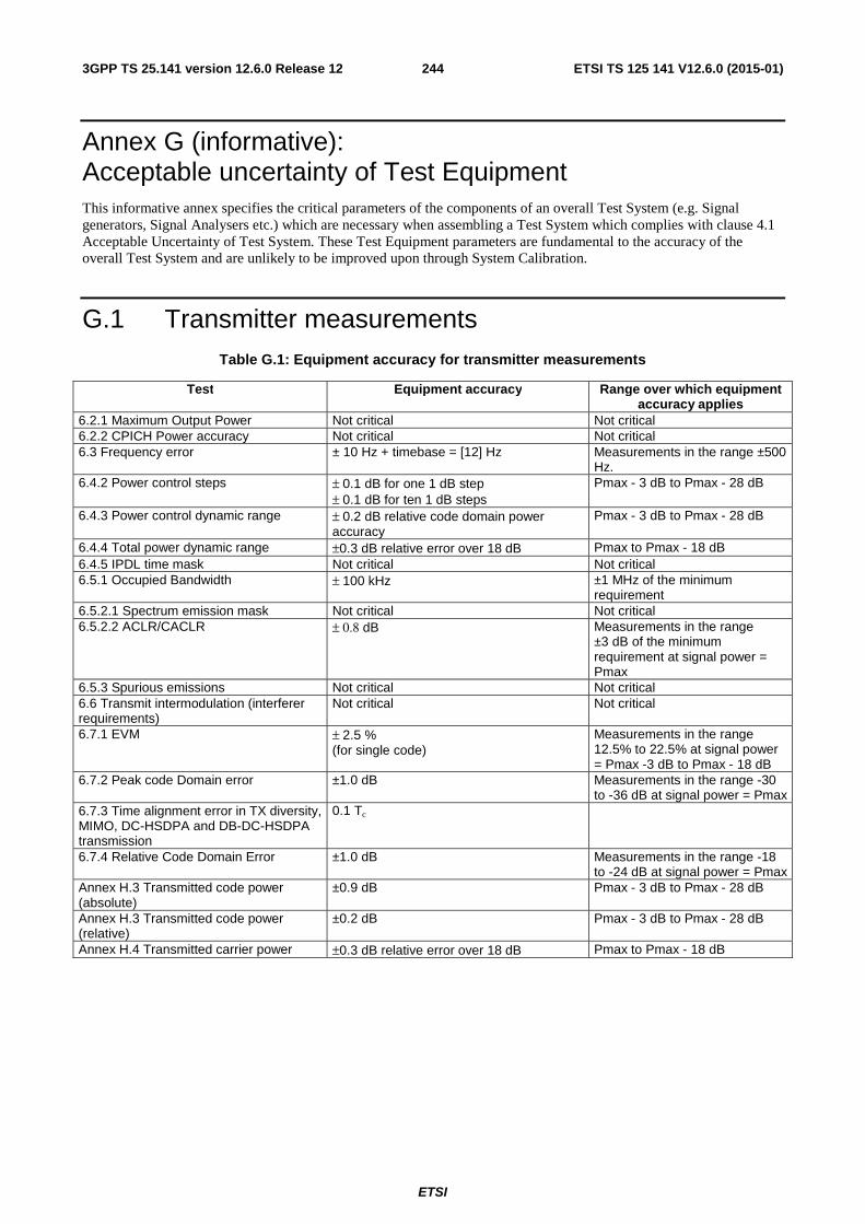
ETSI
ETSI TS 125 141 V12.6.0 (2015-01)2443GPP TS 25.141 version 12.6.0 Release 12
Annex G (informative): Acceptable uncertainty of Test Equipment This informative annex specifies the critical parameters of the components of an overall Test System (e.g. Signal generators, Signal Analysers etc.) which are necessary when assembling a Test System which complies with clause 4.1 Acceptable Uncertainty of Test System. These Test Equipment parameters are fundamental to the accuracy of the overall Test System and are unlikely to be improved upon through System Calibration.
G.1 Transmitter measurements Table G.1: Equipment accuracy for transmitter measurements
Test
Equipment accuracy Range over which equipment accuracy applies
6.2.1 Maximum Output Power Not critical Not critical 6.2.2 CPICH Power accuracy Not critical Not critical 6.3 Frequency error ± 10 Hz + timebase = [12] Hz Measurements in the range ±500
Hz. 6.4.2 Power control steps ± 0.1 dB for one 1 dB step
± 0.1 dB for ten 1 dB steps Pmax - 3 dB to Pmax - 28 dB
6.4.3 Power control dynamic range ± 0.2 dB relative code domain power accuracy
Pmax - 3 dB to Pmax - 28 dB
6.4.4 Total power dynamic range ±0.3 dB relative error over 18 dB Pmax to Pmax - 18 dB 6.4.5 IPDL time mask Not critical Not critical 6.5.1 Occupied Bandwidth ± 100 kHz ±1 MHz of the minimum
requirement 6.5.2.1 Spectrum emission mask Not critical Not critical 6.5.2.2 ACLR/CACLR ± 0.8 dB Measurements in the range
±3 dB of the minimum requirement at signal power = Pmax
6.5.3 Spurious emissions Not critical Not critical 6.6 Transmit intermodulation (interferer requirements)
Not critical Not critical
6.7.1 EVM ± 2.5 % (for single code)
Measurements in the range 12.5% to 22.5% at signal power = Pmax -3 dB to Pmax - 18 dB
6.7.2 Peak code Domain error ±1.0 dB Measurements in the range -30 to -36 dB at signal power = Pmax
6.7.3 Time alignment error in TX diversity, MIMO, DC-HSDPA and DB-DC-HSDPA transmission
0.1 Tc
6.7.4 Relative Code Domain Error ±1.0 dB Measurements in the range -18 to -24 dB at signal power = Pmax
Annex H.3 Transmitted code power (absolute)
±0.9 dB Pmax - 3 dB to Pmax - 28 dB
Annex H.3 Transmitted code power (relative)
±0.2 dB Pmax - 3 dB to Pmax - 28 dB
Annex H.4 Transmitted carrier power ±0.3 dB relative error over 18 dB Pmax to Pmax - 18 dB

ETSI
ETSI TS 125 141 V12.6.0 (2015-01)2453GPP TS 25.141 version 12.6.0 Release 12
G.2 Receiver measurements Table G.2: Equipment accuracy for receiver measurements
Test Equipment accuracy Range over which equipment accuracy applies
7.2 Reference sensitivity level Not critical Not critical 7.3 Dynamic range Not critical Not critical 7.4 Adjacent channel selectivity Not critical Not critical 7.5 Blocking characteristics Not critical Not critical 7.6 Intermod Characteristics Not critical Not critical 7.7 Spurious Emissions Not critical Not critical
G.3 Performance measurements Table G.3: Equipment accuracy for performance measurements
Test Equipment accuracy Range over which equipment accuracy applies
8.2, Demodulation in static propagation condtion
Not critical Not critical
8.3, Demodulation of DCH in multiplath fading conditons
Not critical Not critical
ETSI
ETSI TS 125 141 V12.6.0 (2015-01)2463GPP TS 25.141 version 12.6.0 Release 12
Annex H (Informative): UTRAN Measurement Test Cases
H.1 Purpose of Annex This Annex specifies test specific parameters for some of the UTRAN requirements in chapter 9.2 TS 25.133. The tests provide additional information to how the requirements should be tested. Some requirements may lack a test.
Unless explicitly stated:
- Measurement channel is 12.2 kbps as defined in TS 25.104 annex A, sub-clause A.2 for UL measurements
- Test models defined in TS 25.141 sub-clause 6.1 are used for DL measurements
H.2 Received Total Wideband Power
H.2.1 Absolute RTWP measurement 1. Terminate the BS RX inputs, measure the RTWP and record it.
2. Attach a signal generator to the RX input connector and increase the power until the BS reported RTWP value (Irep) has increased 3 dB.
3. Measure the signal power level delivered from the signal generator. This signal level is now called the "Internally generated noise" (Ni).
4. Sweep the signal generator power such that the sum of internally generated noise (Ni) and signal generator power (I) is swept through the defined conditions range.
5. Check that: |(Ni+I)-Irep| meets the accuracy requirements specified in chapter 9.2.1.1
Note that Iob= (Ni+I)
H.2.2 Relative RTWP measurement 1. Terminate the BS RX inputs, measure the RTWP and record it.
2. Attach a signal generator to the RX input connector and increase the power until the BS reported RTWP value (Irep) has increased 3 dB.
3. Measure the signal power level delivered from the signal generator. This signal level is now called the "Internally generated noise" (Ni).
4. Sweep the signal generator power such that the sum of internally generated noise (Ni) and signal generator power (I) is swept through the defined conditions range.
5. The difference between the reported RTWP values shall meet the accuracy requirements specified in chapter 9.2.1.2.
Note that Iob= (Ni+I)

ETSI
ETSI TS 125 141 V12.6.0 (2015-01)2473GPP TS 25.141 version 12.6.0 Release 12
H.3 Transmitted code power 1. Generate the wanted signal in accordance to test model 2, clause 6.1.1.2. Set power of the DPCH under test to
the Pmax-3 dB level. Power levels for other code channels shall be adjusted as necessary.
2. Measure the output power on code channel under test, Pout,code, at the antenna connector. Record the transmitted code power reported in the BS, Pcode.
3. Check that Pout,code meets the absolute accuracy requirement in TS 25.133 chapter 9.2.5.1. If STTD or closed loop transmit diversity is supported by the BS, the transmitted code power for each branch are measured, summed together and reported to higher layers. In case of TX diversity or MIMO transmission both branches need to be measured and summed together in order to find out the wanted value. The absolute accuracy of Pcode can be accepted if Pout,code will fullfill the following conditions:
Pcode-3.9 dB ≤ Pout,code ≤ Pcode + 3.9 dB, f ≤ 3.0 GHz;
Pcode-4.2 dB ≤ Pout,code ≤ Pcode + 4.2 dB, 3.0 GHz < f ≤ 4.2 GHz
4. Check that the relative accuracy requirement for Pcode in TS 25.133 chapter 9.2.5.2 is met. Set Pcode1 and Pcode2 to transmit with the same power level. The relative accuracy between Pcode1 and Pcode2 can be accepted if the difference between the measured power of one code channel, Pout,code1 and another code
channel Pout,code 2 will fullfill the following conditions:
⏐ Pout,code1 - Pout,code2 ⏐ ≤ 2.2 dB.
5. Set the power of the DPCH under test to the minimum power of the power control dynamic range and repeat steps 2, 3 and 4.
H.4 Transmitted carrier power 1) Set the BS to transmit with the maximum transmission power and measure the output power at the antenna
connector, PMTP. Maximum transmission power is the mean power on one carrier measured at the antenna connector with the code level settings that according to the base station manufacturer will result in an output power of nominally the maximum output power in a specified reference condition. Test model 2, clause 6.1.1.2, when the code powers are set according to table 6.3. shall be used.
2) Operate the BS in closed loop power control until the output power has reached a stable state. Measure the output power, Pout, at the antenna connector and record the transmitted carrier power measured and reported in the BS, Prep. Note that Prep is normalised to the output power measured in Test Model 2 with all codes at their default levels. If STTD or closed loop transmit diversity is supported by the BS, only the highest of the transmit powers is reported to higher layers. In case of TX diversity or MIMO transmission both branches need to be measured in order to find out which one is the highest.
3) Check that the Pout meets the requirement in TS 25.133 chapter 9.2.4.1, with the same test equipment accuracy as in chapter 6.4.4. in TS 25.141. Prep can be accepted if Pout will fullfill the following conditions:
( ) ( ) 3.0log103.0log10 100
5Pr
100
5Pr ++≤≤−+ +− epepPMTPPoutPMTP [ dBm]
4) Repeat step 2 and 3 over the 5%-95% range of the Prep. Use first the standard code powers of test model 2 to verify the Prep range from 50% to 95%. After that put the other dedicated channels off and reduce the powers of the control codes in order to be able to verify the Prep range from 5% to 50%.
NOTE: Pout shall be tested immediately after PMTP in order to avoid the influence of long term stability variation to measurement results.

ETSI
ETSI TS 125 141 V12.6.0 (2015-01)2483GPP TS 25.141 version 12.6.0 Release 12
Annex I (normative): Characteristics of the W-CDMA interference signal The W-CDMA interference signal shall be a DPCH containing the DPCCH and one DPDCH. The data content for each channelization code shall be uncorrelated with each other and to the wanted signal and spread and modulated according to clause 4 of TS25.213 [14]. Further characteristics of DPDCH and DPCCH are specified in table I.1.
Table I.1.: Characteristics of the W-CDMA interference signal
Channel Bit Rate Spreading Factor Channelization Code
Relative Power
DPDCH 240 kbps 16 4 0 dB DPCCH 15 kbps 256 0 -5.46 dB
NOTE: The DPDCH and DPCCH settings are chosen to simulate a signal with realistic Peak to Average Ratio.

ETSI
ETSI TS 125 141 V12.6.0 (2015-01)2493GPP TS 25.141 version 12.6.0 Release 12
Annex J (informative): Change history
TSG Doc CR R Title Cat Curr New Work Item RP-37 Rel-8 version created based on v7.9.0 8.0.0 RP-37 RP-070658 0461 Introduction of UMTS1500 requirements B 7.9.0 8.0.0 RInImp8-
UMTS1500 RP-38 RP-070936 0466 1 Base Station MIMO corrections A 8.0.0 8.1.0 MIMO-RF RP-38 RP-070937 0468 Spurious emissions limits for coexistance with
CDMA850 A 8.0.0 8.1.0 TEI7
RP-39 RP-080120 0478 Correction to RX spurious emissions A 8.1.0 8.2.0 TEI6 RP-39 RP-080122 0473 1 Editorial modifications of the test requirement
table for the demodulation of E-DPDCH in multipath fading conditions and table and figure title in A.18 in 25.141
A 8.1.0 8.2.0 TEI7
RP-39 RP-080124 0471 1 Introduction of UMTS700 requirements (Band XII, XIII and XIV) in TS 25.141
B 8.1.0 8.2.0 RInImp8-UMTS700
RP-39 RP-080126 0469 1 Correction of the node for Band XI BS ACLR F 8.1.0 8.2.0 RInImp8-UMTS1500
RP-39 RP-080126 0470 Correction of spurious emissions limits for coexistence with CDMA850
F 8.1.0 8.2.0 TEI8
RP-40 RP-080326 0479 2 Correction on emission requirements for protection of public safety operations
F 8.2.0 8.3.0 RInImp8-UMTS700
RP-41 RP-080632 0480 Corrections on the section on BS using antenna array
F 8.3.0 8.4.0 MIMO-RF
RP-42 RP-080904 0485 Clarification on HS-SCCH structure for Test Model 6
F 8.4.0 8.5.0 TEI7
RP-42 RP-080904 0491 3 Clarification for test model 1 F 8.4.0 8.5.0 TEI7 RP-42 RP-080927 0487 1 Clarification of eNB HST propagation conditions
(25.141, rel-7) F 8.4.0 8.5.0 TEI7
RP-42 RP-080948 0489 1 TS 25.141 modification due to DC HSDPA B 8.4.0 8.5.0 RANimp-DCHSDPA
RP-42 RP-080945 481 Transmitter characteristics Tests for 3G Home NodeB
F 8.4.0 8.5.0 HNB-RF
RP-42 RP-080945 492 1 Regional requirement on Home Node B applicability
F 8.4.0 8.5.0 HNB-RF
RP-42 RP-080945 482 Receiver characteristics Tests for 3G Home NodeB
F 8.4.0 8.5.0 HNB-RF
RP-42 RP-080945 483 Demodulation Requirements Tests for 3G Home NodeB
F 8.4.0 8.5.0 HNB-RF
RP-42 RP-080945 493 Modified Test Models for 3G Home NodeB F 8.4.0 8.5.0 HNB-RF RP-43 RP-090197 496 Co-existence requirement for the band
1880MHz F 8.5.0 8.6.0 RInImp9-
UMTS1880TDD
RP-43 RP-090192 494 Change reference bandwidth for ACLR limit for Home BS
F 8.5.0 8.6.0 HNB-RF
RP-43 RP-090192 495 3G Home NodeB Transmit Power Conformance Testing for Adjacent Channel Protection
F 8.5.0 8.6.0 HNB-RF
RP-44 RP-090553 499 Correction of local area base station coexistence spurious emission requirements
F 8.6.0 8.7.0 RInImp9-UMTS1880TDD
RP-44 RP-090605 497 Correction on Home BS Output Power Requirements for Adjacent Channel Protection
F 8.6.0 8.7.0 HNB-RF
RP-44 RP-090605 502 Correction on test system uncertainty for Home BS absolute ACLR limit
F 8.6.0 8.7.0 HNB-RF
RP-44 RP-090559 498 Introduction of Extended UMTS800 requirements
B 8.7.0 9.0.0 Rlnlmp9-UMTSLTE800
RP-45 RP-090827 516 1 Correction of DPCCH slot format for FRC8 A 9.0.0 9.1.0 TEI7 RP-45 RP-090825 505 Spectrum emission mask test tolerance correction A 9.0.0 9.1.0 TEI8 RP-45 RP-090825 509 Correction of Receiver additional spurious emission
requirement A 9.0.0 9.1.0 TEI8
RP-45 RP-090824 511 Editorial correction on 6.5.3.7 F 9.0.0 9.1.0 TEI9
RP-46 RP-091286 517
Introduction of Extended UMTS1500 requirements for TS25.141 (Technically endorsed at RAN 4 52bis in R4-093628) B 9.1.0 9.2.0 UMTSLTE1500

ETSI
ETSI TS 125 141 V12.6.0 (2015-01)2503GPP TS 25.141 version 12.6.0 Release 12
RP-46 RP-091276 519 Testing in case of Rx diversity, Tx diversity and MIMO (Technically endorsed at RAN 4 52bis in R4-093983) A 9.1.0 9.2.0 TEI8
RP-46 RP-091288 520 Introduction of the BS requirements for DC-HSUPA (Technically Endorsed in R4-52, R4-093331) B 9.1.0 9.2.0
RANimp-DC_HSUPA
RP-46 RP-091289 521 Introduction of BS requirements for DB-DC-HSDPA (Technically Endorsed in R4-52, R4-093416) B 9.1.0 9.2.0
RANimp-MultiBand_DC_HSDPA
RP-46 RP-091277 523 Corrections on additional spectrum emission limits for Bands XII, XIII, XIV A 9.1.0 9.2.0 TEI8
RP-46 RP-091296 524 1 Correction to the transmitter intermodulation F 9.1.0 9.2.0 TEI9
RP-46 RP-091296 527 1 Time alignment error definition correction for DC-HSDPA A 9.1.0 9.2.0 TEI9
RP-46 RP-091268 529 1 Protection of E-UTRA for UTRA BS A 9.1.0 9.2.0 LTE-RF RP-47 RP-100261 537 Corrections on Home BS Output Power Conformance
Testing A 9.2.0 9.3.0 TEI8
RP-47 RP-100261 539 1 TS 25.141 Removal of testing for receiver diversity port
A 9.2.0 9.3.0 TEI8
RP-47 RP-100272 535 1 Clarification of time alignment error requirements F 9.2.0 9.3.0 TEI9 RP-47 RP-100263 540 1 Introduction of Band XX in 25.141 B 9.2.0 9.3.0 RInImp9-
UMTSLTE800EU
RP-47 RP-100264 534 Corrections for Extended UMTS1500 requirements
F 9.2.0 9.3.0 UMTSLTE1500
RP-47 RP-100267 542 Tx-Rx frequency separation for DC-HSUPA B 9.2.0 9.3.0 RANimp-DC_HSUPA
RP-48 RP-100625 548 Clarification of applicability of requirements for multi-carrier BS
F 9.3.0 9.4.0 RInImp9-RFmulti
RP-48 RP-100626 543 Correction of blocking performance requirement when co-located with BS in other bands (Band 20)
F 9.3.0 9.4.0 RInImp9-UMTSLTE800EU
RP-48 RP-100631 549 Correction of RACH message demodulation requirement definitions
F 9.3.0 9.4.0 TEI9
RP-48 RP-100631 547 1 Co-existence with services in adjacent frequency bands
F 9.3.0 9.4.0 TEI9
RP-49 RP-100918 551 Corrections on Home BS spurious emission limits for co-existence with Home BS operating in other bands
A 9.4.0 9.5.0 HNB-RF
RP-49 RP-100918 553 Clarifications on Base Station transmit and receive configurations
A 9.4.0 9.5.0 TEI8
RP-50 RP-101334 566 1 Band XII channel arrangement correction on 25.141
A 9.5.0 9.6.0 TEI8
RP-50 RP-101340 561 1 Revision of Time Alignment Error requirement testing
F 9.5.0 9.6.0 TEI9
RP-50 RP-101353 563 Introduction of frequency bands for 4C-HSDPA B 9.6.0 10.0.0 4c_HSDPA-Core
RP-50 RP-101353 562 1 Revision of Time Alignment Error requirement testing
B 9.6.0 10.0.0 4C_HSDPA-Core
RP-50 RP-101361 558 Protection of E-UTRA Band 24 B 9.6.0 10.0.0 L_Band_LTE_ATC_MSS-Core
RP-51 RP-110355 0564 2 DB-DC-HSDPA: New band combinations B 10.0.0 10.1.0 DB_DC_HSDPA-Core
RP-51 RP-110341 0573 - Clarification of ambiguity in Test Model 5 A 10.0.0 10.1.0 TEI8
RP-51 RP-110352 0576 1 Correction of the test port description for TS 25.141 Rel-10 F 10.0.0 10.1.0 TEI10
RP-51 RP-110352 0577 1 UTRA BS Receiver spurious requirements for protection of other bands F 10.0.0 10.1.0 TEI10
RP-51 RP-110352 0578 1 Harmonization of co-existence/co-location requirements between 25.141 and 36.141 F 10.0.0 10.1.0 TEI10
RP-52 RP-110788 583 Modifications to Band 3 to allow LTE Band 3 operation in Japan (Rel-10 TS25.141 CR)
A 10.1.0 10.2.0 TEI8
RP-52 RP-110804 584 Add coexistence requirements for expanded 1900MHz band in 25.141
B 10.1.0 10.2.0 E1900_UB-Core
RP-52 RP-110813 585 Add 2GHz S-Band (Band 23) in 25.141 B 10.1.0 10.2.0 S_Band_LTE_ATC_MSS-Perf
RP-52 RP-110800 586 Definition of Virtual Antenna Mapping (VAM) and applicability of S-CPICH power accuracy requirement
B 10.1.0 10.2.0 MIMO_HSDPA-Core

ETSI
ETSI TS 125 141 V12.6.0 (2015-01)2513GPP TS 25.141 version 12.6.0 Release 12
RP-53 RP-111255 592 Add Band 42 and 43 for LTE 3500 (TDD) to TS 25.141
B 10.2.0 10.3.0 RInImp8-UMTSLTE3500
RP-53 RP-111255 593 1 Add Band 22/XXII for LTE/UMTS 3500 (FDD) to TS 25.141
B 10.2.0 10.3.0 RInImp8-UMTSLTE3500
RP-53 RP-111262 588 Co-existence requirements on TS 25.141 F 10.2.0 10.3.0 TEI10 RP-53 RP-111268 587 1 Updating BS Coexistence table for Band 23 in
25.141 B 10.2.0 10.3.0 S_Band_LTE
_ATC_MSS-Perf
RP-53 RP-111270 594 1 Introduction of S-CPICH power offset accuracy test
B 10.2.0 10.3.0 4C_HSDPA-Perf
RP-54 RP-111686 595 Removal of TBD in the S-CPICH power offset test F 10.3.0 10.4.0 MIMO_HSDPA-Core, TEI10
RP-54 RP-111734 596 Band 42 and 43 for LTE 3500 (TDD) correction to TS 25.141
F 10.3.0 10.4.0 TEI10
RP-54 RP-111686 597 Introduction of HS-DPCCH demodulation performance testing for 4C-HSDPA
F 10.3.0 10.4.0 4C_HSDPA-Perf, TEI10
RP-54 RP-111734 598 Clarification of general blocking requirements for co-existence in TS 25.141
F 10.3.0 10.4.0 TEI10
RP-54 RP-111687 600 3 TX ON or OFF CR 25.141 F 10.3.0 10.4.0 TEI10 RP-54 RP-111696 599 1 Introduction of new configuration for 4C-HSDPA B 10.4.0 11.0.0 4C_HSDPA_Co
nfig-Core RP-55 RP-120305 605 Introduction of Band 26/XXVI to TS 25. 141 B 11.0.0 11.1.0 e850_UB-
Core RP-55 RP-120301 606 MC DB HSDPA: Introduction of configurations I-
2-VIII-2 and II-1-V-2 in TS 25.141 B 11.0.0 11.1.0 HSDPA_DB_
MC-Core RP-55 RP-120297 607 Correction of frequency range for spurious
emission requirements A 11.0.0 11.1.0 RInImp8-
UMTSLTE3500
RP-55 RP-120339 0608 Addition of Band 23 HeNB specifications in 25.141
A 11.0.0 11.1.0 S_Band_LTE_ATC_MSS-Core
RP-56 RP-120787 0609 Introduction of non-contiguous operation for 4C-HSDPA
B 11.1.0 11.2.0 NC_4C_HSDPA
RP-56 RP-120786 0610 1 8C-HSDPA: Introduction of BS conformance testing for 8C-HSDPA operation
B 11.1.0 11.2.0 8C_HSDPA-Core
RP-56
RP-120783
0612 1
Update to Regional Requirements table 25.141 – CR Not implemented as the content is not from this spec but from 25.104 A 11.1.0 TEI10
RP-56 RP-120771 0616 Introduction of Japanese Regulatory Requirements to W-CDMA Band VIII (R11)
A 11.1.0 11.2.0 TEI9
RP-56 RP-120793 0619 Introduction of Band 28 B 11.1.0 11.2.0 LTE_APAC700-Core
RP-56 RP-120793 0620 Introduction of Band 44 B 11.1.0 11.2.0 LTE_APAC700-Core
RP-56 RP-120792 0621 2 Introduction of E850_LB (Band 27) to TS 25.141
B 11.1.0 11.2.0 LTE_e850_LB-Perf
RP-56 RP-120766 0625 Correction of PHS protection requirements for TS 25.141
A 11.1.0 11.2.0 TEI8
RP-57 RP-121314 626 Alignment of NC-4C-HSDPA configurations table
F 11.2.0 11.3.0 NC_4C_HSDPA-Core
RP-57 RP-121316 627 1 Update of co-location spurious emission in TS 25.141
F 11.2.0 11.3.0 LTE_APAC700-Core
RP-57 RP-121300 631 Modificaitions of frequency ranges on spurious emission requirements for Band 6, 18, 19
A 11.2.0 11.3.0 RInImp9-UMTSLTE800
RP-57 RP-121301 634 Band VIII ACLR A 11.2.0 11.3.0 TEI9 RP-57 RP-121312 636 BS test uncertainties above 3 GHz A 11.2.0 11.3.0 RInImp8-
UMTSLTE3500
RP-58 RP-121848 0640 - Introducing the additional frequency bands of 5 MHz x 2 in 1.7 GHz in Japan to Band III
A 11.3.0 11.4.0 RInImp-UMTS1700
RP-58 RP-121909 0641 - Correct f_offsetmax definition for a BS operating in non-contiguous spectrum in TS 25.141
F 11.3.0 11.4.0 NC_4C_HSDPA-Perf
RP-58 RP-121902 0642 - Introduction of Band 29 B 11.3.0 11.4.0 LTE_DL_FDD700-Perf
RP-60 RP-130768 643 Introduction of dual-band 4C-HSDPA configuration for Band I and VIII
B 11.4.0 11.5.0 HSDPA_DB_MC-Perf

ETSI
ETSI TS 125 141 V12.6.0 (2015-01)2523GPP TS 25.141 version 12.6.0 Release 12
RP-60 RP-130764 645 2X2MIMO: BS conformance testing for S-CPICH
A 11.4.0 11.5.0 TEI10
RP-60 RP-130768 646 Correction to Definitions list F 11.4.0 11.5.0 8C_HSDPA-Core
RP-60 RP-130800 647 1 Indication of HSDPA Multiflow BS performance requirements
B 11.4.0 11.5.0 HSDPA_MFTX-Perf
RP-60 RP-130792 648 1 Introduction of Band 30 B 11.5.0 12.0.0 LTE_WCS_band-Perf
RP-60 RP-130790 649 1 Introduction of LTE 450 into TS 25.141 B 11.5.0 12.0.0 LTE450_Brazil-Core
RP-61 RP-131293 655 Correction on TX-RX sepration for TS25.141 A 12.0.0 12.1.0 TEI11 RP-61 RP-131283 656 Co-location requirements for E-UTRA Medium Range
BS F 12.0.0 12.1.0 medBS_class_
LTE_MSR-Core RP-61 RP-131293 658 Correction on Base station maximum output power for
TS25.141 A 12.0.0 12.1.0 TEI11
RP-61 RP-131287 661 Introduction of MIMO mode with 4 transmit antennas A 12.0.0 12.1.0 4Tx_HSDPA-Perf
RP-61 RP-131288 662 Introduction of BS demodulation performance requirements for HSUPA MIMO
A 12.0.0 12.1.0 MIMO_64QAM_HSUPA-Perf
RP-62 RP-131967 667 1 Alignment of Note related to BS Spurious emissions limits for co-location with another BS
F 12.1.0 12.2.0 TEI12
RP-62 RP-131929 670 1 Correction of the terminology used for MIMO mode with two transmit antennas
A 12.1.0 12.2.0 4Tx_HSDPA-Perf
RP-62 RP-131930 672 Clarification for CACLR in TS25.141 A 12.1.0 12.2.0 medBS_class_LTE_MSR-Perf
RP-63 RP-140368 675 Correction on tested frequency range A 12.2.0 12.3.0 TEI10 RP-64 RP-140926 683 1 Introduction of operating band XXXII In TS25.141 B 12.3.0 12.4.0 LTE_UTRA_SD
L_BandL-Perf RP-65 RP-141562 695 - CR for RTWP tests (Rel-12) A 12.4.0 12.5.0 TEI12 RP-65 RP-141562 696 - Update of definitions to support supplemental DL in
TS25.141 F 12.4.0 12.5.0 TEI12
RP-66 RP-142145 704 Absolute ACLR limit for UTRA A 12.5.0 12.6.0 NC_4C_HSDPA-Perf
RP-66 RP-142149 707 Introduction of multi-carrier multi-band BS testing in TS 25.141 - clauses 1-5 This CR removes several sevtion (by mistake). This change does not appear in the Cat-F CR. This change was thus not implemented.
A 12.5.0 12.6.0 TEI11
RP-66 RP-142149 708 Introduction of multi-carrier and multi-band BS testing in TS 25.141 - clauses 6-7
A 12.5.0 12.6.0 TEI11

ETSI
ETSI TS 125 141 V12.6.0 (2015-01)2533GPP TS 25.141 version 12.6.0 Release 12
History
Document history
V12.5.0 October 2014 Publication
V12.6.0 January 2015 Publication
Related Documents