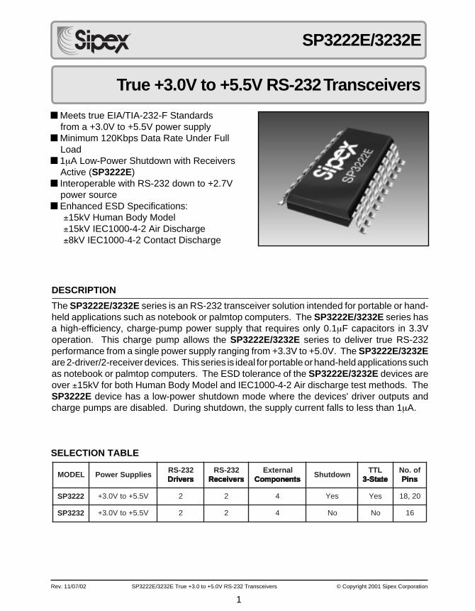
1 Rev. 11/07/02 SP3222E/3232E True +3.0 to +5.0V RS-232 Transceivers © Copyright 2001 Sipex Corporation True +3.0V to +5.5V RS-232 Transceivers SP3222E/3232E DESCRIPTION ■ Meets true EIA/TIA-232-F Standards from a +3.0V to +5.5V power supply ■ Minimum 120Kbps Data Rate Under Full Load ■ 1μA Low-Power Shutdown with Receivers Active (SP3222E) ■ Interoperable with RS-232 down to +2.7V power source ■ Enhanced ESD Specifications: ±15kV Human Body Model ±15kV IEC1000-4-2 Air Discharge ±8kV IEC1000-4-2 Contact Discharge The SP3222E/3232E series is an RS-232 transceiver solution intended for portable or hand- held applications such as notebook or palmtop computers. The SP3222E/3232E series has a high-efficiency, charge-pump power supply that requires only 0.1μF capacitors in 3.3V operation. This charge pump allows the SP3222E/3232E series to deliver true RS-232 performance from a single power supply ranging from +3.3V to +5.0V. The SP3222E/3232E are 2-driver/2-receiver devices. This series is ideal for portable or hand-held applications such as notebook or palmtop computers. The ESD tolerance of the SP3222E/3232E devices are over ±15kV for both Human Body Model and IEC1000-4-2 Air discharge test methods. The SP3222E device has a low-power shutdown mode where the devices' driver outputs and charge pumps are disabled. During shutdown, the supply current falls to less than 1μA. SELECTION TABLE L E D O M s e i l p p u S r e w o P 2 3 2 - S R s r e v i r D s r e v i r D s r e v i r D s r e v i r D s r e v i r D 2 3 2 - S R s r e v i e c e R s r e v i e c e R s r e v i e c e R s r e v i e c e R s r e v i e c e R l a n r e t x E s t n e n o p m o C s t n e n o p m o C s t n e n o p m o C s t n e n o p m o C s t n e n o p m o C n w o d t u h S L T T e t a t S - 3 e t a t S - 3 e t a t S - 3 e t a t S - 3 e t a t S - 3 f o . o N s n i P s n i P s n i P s n i P s n i P 2 2 2 3 P S V 5 . 5 + o t V 0 . 3 + 2 2 4 s e Y s e Y 0 2 , 8 1 2 3 2 3 P S V 5 . 5 + o t V 0 . 3 + 2 2 4 o N o N 6 1 ®

Welcome message from author
This document is posted to help you gain knowledge. Please leave a comment to let me know what you think about it! Share it to your friends and learn new things together.
Transcript
1
Rev. 11/07/02 SP3222E/3232E True +3.0 to +5.0V RS-232 Transceivers © Copyright 2001 Sipex Corporation
True +3.0V to +5.5V RS-232 Transceivers
SP3222E/3232E
DESCRIPTION
Meets true EIA/TIA-232-F Standardsfrom a +3.0V to +5.5V power supply
Minimum 120Kbps Data Rate Under FullLoad
1µA Low-Power Shutdown with ReceiversActive (SP3222E)
Interoperable with RS-232 down to +2.7Vpower source
Enhanced ESD Specifications: ±15kV Human Body Model ±15kV IEC1000-4-2 Air Discharge ±8kV IEC1000-4-2 Contact Discharge
The SP3222E/3232E series is an RS-232 transceiver solution intended for portable or hand-held applications such as notebook or palmtop computers. The SP3222E/3232E series hasa high-efficiency, charge-pump power supply that requires only 0.1µF capacitors in 3.3Voperation. This charge pump allows the SP3222E/3232E series to deliver true RS-232performance from a single power supply ranging from +3.3V to +5.0V. The SP3222E/3232Eare 2-driver/2-receiver devices. This series is ideal for portable or hand-held applications suchas notebook or palmtop computers. The ESD tolerance of the SP3222E/3232E devices areover ±15kV for both Human Body Model and IEC1000-4-2 Air discharge test methods. TheSP3222E device has a low-power shutdown mode where the devices' driver outputs andcharge pumps are disabled. During shutdown, the supply current falls to less than 1µA.
SELECTION TABLE
LEDOM seilppuSrewoP232-SRsrevirD srevirD srevirD srevirD srevirD
232-SRsrevieceR srevieceR srevieceR srevieceR srevieceR
lanretxEstnenopmoC stnenopmoC stnenopmoC stnenopmoC stnenopmoC
nwodtuhSLTT
etatS-3 etatS-3 etatS-3 etatS-3 etatS-3fo.oN
sniP sniP sniP sniP sniP
2223PS V5.5+otV0.3+ 2 2 4 seY seY 02,81
2323PS V5.5+otV0.3+ 2 2 4 oN oN 61
®

Rev. 11/07/02 SP3222E/3232E True +3.0 to +5.0V RS-232 Transceivers © Copyright 2002 Sipex Corporation
2
RETEMARAP .NIM .PYT .XAM STINU SNOITIDNOC
SCITSIRETCARAHCCD
tnerruCylppuS 3.0 0.1 Am T,daolon BMA 52+= o V,C CC V3.3=
tnerruCylppuSnwodtuhS 0.1 01 µA ,DNG=NDHS T BMA 52+= o V,C CC V3.3+=
STUPTUOREVIECERDNASTUPNICIGOL
WOLdlohserhTcigoLtupnI 8.0 V 2etoN,NDHS,NE,NIxT
HGIHdlohserhTcigoLtupnI 0.24.2
V V CC 2etoN,V3.3=V CC 2etoN,V0.5=
tnerruCegakaeLtupnI 10.0± 0.1± µA ,NDHS,NE,NIxT T BMA 52+= oC
tnerruCegakaeLtuptuO 50.0± 01± µA delbasidsreviecer
WOLegatloVtuptuO 4.0 V I TUO Am6.1=
HGIHegatloVtuptuO V CC 6.0- V CC 1.0- V I TUO Am0.1-=
STUPTUOREVIRD
gniwSegatloVtuptuO 0.5± 4.5± V k3 Ω ,stuptuorevirdllatadnuorgotdaolT BMA 52+= oC
ecnatsiseRtuptuO 003 Ω V CC T,V0=-V=+V= TUO = + V2
tnerruCtiucriC-trohStuptuO 53±07±
06±001±
AmAm
V TUO V0=V TUO = + V51
tnerruCegakaeLtuptuO 52± µA V TUO = + V,V21 CC delbasidsrevird,V5.5otV0=
NOTE 1: V+ and V- can have maximum magnitudes of 7V, but their absolute difference cannot exceed 13V.
ABSOLUTE MAXIMUM RATINGSThese are stress ratings only and functional operation of thedevice at these ratings or any other above those indicated inthe operation sections of the specifications below is notimplied. Exposure to absolute maximum rating conditionsfor extended periods of time may affect reliability and causepermanent damage to the device.
VCC
................................................................-0.3V to +6.0VV+ (NOTE 1)................................................-0.3V to +7.0VV- (NOTE 1)................................................+0.3V to -7.0VV+ + |V-| (NOTE 1)....................................................+13V
ICC
(DC VCC
or GND current).................................±100mA
Input VoltagesTxIN, EN ................................................... -0.3V to +6.0VRxIN ..........................................................................±15V
Output VoltagesTxOUT ......................................................................±15VRxOUT ........................................... -0.3V to (V
CC + 0.3V)
Short-Circuit DurationTxOUT ............................................................ Continuous
Storage Temperature .............................. -65°C to +150°C
Power Dissipation Per Package20-pin SSOP (derate 9.25mW/oC above +70oC) ..... 750mW18-pin PDIP (derate 15.2mW/oC above +70oC) .... 1220mW18-pin SOIC (derate 15.7mW/oC above +70oC) ... 1260mW20-pin TSSOP (derate 11.1mW/oC above +70oC) .. 890mW16-pin SSOP (derate 9.69mW/oC above +70oC) ..... 775mW16-pin PDIP (derate 14.3mW/oC above +70oC) .... 1150mW16-pin Wide SOIC (derate 11.2mW/oC above +70oC) 900mW16-pin TSSOP (derate 10.5mW/oC above +70oC) .. 850mW16-pin nSOIC (derate 13.57mW/°C above +70°C) .. 1086mW
SPECIFICATIONSUnless otherwise noted, the following specifications apply for V
CC = +3.0V to +5.0V with T
AMB = T
MIN to T
MAX

3
Rev. 11/07/02 SP3222E/3232E True +3.0 to +5.0V RS-232 Transceivers © Copyright 2001 Sipex Corporation
RETEMARAP .NIM .PYT .XAM STINU SNOITIDNOC
STUPNIREVIECER
egnaRegatloVtupnI 51- 51+ V
WOLdlohserhTtupnI 6.08.0
2.15.1
V V CC V3.3=V CC V0.5=
HGIHdlohserhTtupnI 5.18.1
4.24.2
V V CC V3.3=V CC V0.5=
siseretsyHtupnI 3.0 V
ecnatsiseRtupnI 3 5 7 kΩ
SCITSIRETCARAHCGNIMIT
etaRataDmumixaM 021 532 spbk RL k3= Ω C, L gnihctiwsrevirdeno,Fp0001=
yaleDnoitagaporPrevirD 0.10.1
µsµs
t LHP R, L K3= Ω C, L Fp0001=t HLP R, L K3= Ω C, L Fp0001=
yaleDnoitagaporPrevieceR 3.03.0
µs t LHP C,TUOxRotNIxR, L Fp051=t HLP C,TUOxRotNIxR, L Fp051=
emiTelbanEtuptuOrevieceR 002 sn
emiTelbasiDtuptuOrevieceR 002 sn
wekSrevirD 001 005 sn t| LHP t- HLP T,| BMA 52= oC
wekSrevieceR 002 0001 sn t| LHP t- HLP |
etaRwelSnoigeR-noitisnarT 03 /V µs V CC R,V3.3= L K3= Ω T, BMA 52= o ,CV0.3+otV0.3-morfnekatstnemerusaem
V0.3-otV0.3+ro
SPECIFICATIONS (continued)Unless otherwise noted, the following specifications apply for V
CC = +3.0V to +5.0V with T
AMB = T
MIN to T
MAX.
Typical Values apply at VCC
= +3.3V or +5.0V and TAMB
= 25oC.
NOTE 2: Driver input hysteresis is typically 250mV.

Rev. 11/07/02 SP3222E/3232E True +3.0 to +5.0V RS-232 Transceivers © Copyright 2002 Sipex Corporation
4
Figure 1. Transmitter Output Voltage VS. LoadCapacitance for the SP3222 and the SP3232
Figure 2. Slew Rate VS. Load Capacitance for theSP3222 and the SP3232
Figure 3. Supply Current VS. Load Capacitance whenTransmitting Data for the SP3222 and the SP3232
TYPICAL PERFORMANCE CHARACTERISTICSUnless otherwise noted, the following performance characteristics apply for V
CC = +3.3V, 120kbps data rates, all drivers
loaded with 3kΩ, 0.1µF charge pump capacitors, and TAMB
= +25°C.
14
12
10
8
6
4
2
0
Sle
w R
ate
[V/µ
s]
Load Capacitance [pF]
+Slew-Slew
0 500 1000 1500 2000 2330
50
45
40
35
30
25
20
15
10
5
0
Su
pp
ly C
urr
ent
[mA
]
Load Capacitance [pF]
118KHz60KHz10KHz
0 500 1000 1500 2000 2330
6
4
2
0
-2
-4
-6
Tran
smitt
er O
utpu
t Vol
tag
e [V
]
Load Capacitance [pF]
Vout+Vout-
500 1000 1500 20000
5
Rev. 11/07/02 SP3222E/3232E True +3.0 to +5.0V RS-232 Transceivers © Copyright 2001 Sipex Corporation
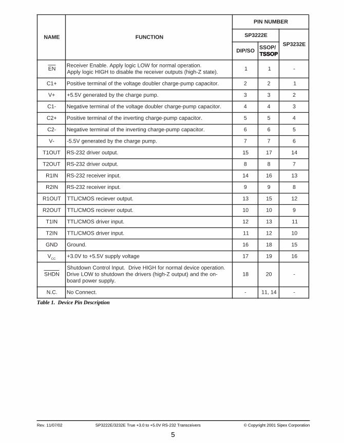
EMAN NOITCNUF
REBMUNNIP
E2223PS
E2323PSOS/PID
-/POSSPOSST POSST POSST POSST POSST
NE.noitarepolamronrofWOLcigolylppA.elbanErevieceR
.)etatsZ-hgih(stuptuoreviecerehtelbasidotHGIHcigolylppA1 1 -
+1C .roticapacpmup-egrahcrelbuodegatlovehtfolanimretevitisoP 2 2 1
+V .pmupegrahcehtybdetarenegV5.5+ 3 3 2
-1C .roticapacpmup-egrahcrelbuodegatlovehtfolanimretevitageN 4 4 3
+2C .roticapacpmup-egrahcgnitrevniehtfolanimretevitisoP 5 5 4
-2C .roticapacpmup-egrahcgnitrevniehtfolanimretevitageN 6 6 5
-V .pmupegrahcehtybdetarenegV5.5- 7 7 6
TUO1T .tuptuorevird232-SR 51 71 41
TUO2T .tuptuorevird232-SR 8 8 7
NI1R .tupnireviecer232-SR 41 61 31
NI2R .tupnireviecer232-SR 9 9 8
TUO1R .tuptuoreveicerSOMC/LTT 31 51 21
TUO2R .tuptuoreveicerSOMC/LTT 01 01 9
NI1T .tupnirevirdSOMC/LTT 21 31 11
NI2T .tupnirevirdSOMC/LTT 11 21 01
DNG .dnuorG 61 81 51
V CC egatlovylppusV5.5+otV0.3+ 71 91 61
NDHS.noitarepoecivedlamronrofHGIHevirD.tupnIlortnoCnwodtuhS
-noehtdna)tuptuoZ-hgih(srevirdehtnwodtuhsotWOLevirD.ylppusrewopdraob
81 02 -
.C.N .tcennoCoN - 41,11 -
Table 1. Device Pin Description

Rev. 11/07/02 SP3222E/3232E True +3.0 to +5.0V RS-232 Transceivers © Copyright 2002 Sipex Corporation
6
V-
1
2
3
4 13
14
15
16
5
6
7
12
11
10
C1+
V+
C1-
C2+
C2-
R1IN
R2IN
GND
VCC
T1OUT
T2IN
8 9
SP3232E
T1IN
R1OUT
R2OUT
T2OUT
Figure 5. Pinout Configuration for the SP3232E
Figure 4. Pinout Configurations for the SP3222E
V-
1
2
3
4 17
18
19
20
5
6
7
16
15
14
SHDN
C1+
V+
C1-
C2+
C2-
N.C.
EN
R1IN
GND
VCC
T1OUT
N.C.
8
9
10 11
12
13
R2IN
R2OUT
SP3222E
T2OUT T1IN
T2IN
R1OUT
SSOP/TSSOP
V-
1
2
3
4 15
16
17
18
5
6
7
14
13
12
SHDN
C1+
V+
C1-
C2+
C2-
EN
R1IN
GND
VCC
T1OUT
8
9 10
11
R2IN
SP3222E
T2OUT T2IN
T1IN
R1OUT
DIP/SO
R2OUT
7
Rev. 11/07/02 SP3222E/3232E True +3.0 to +5.0V RS-232 Transceivers © Copyright 2001 Sipex Corporation
SP3232E
1
3
5
4
2
6
16
GND
T1IN
T2IN
T1OUT
T2OUT
C1+
C1-
C2+
C2-
V+
V-
VCC
11
10
0.1µF
0.1µF
0.1µF+
C2
C5
C1
+
+*C3
C4
+
+
0.1µF
0.1µF
14
7RS-232OUTPUTS
RS-232INPUTS
LOGICINPUTS
VCC
15
5kΩ
R1INR1OUT12 13
5kΩ
R2INR2OUT9 8
LOGICOUTPUTS
*can be returned to either VCC or GND
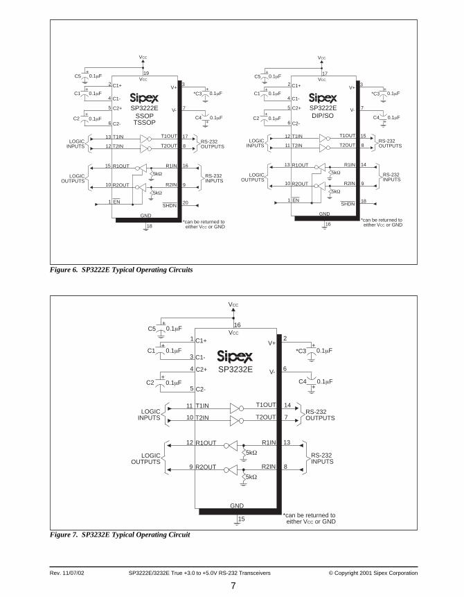
Figure 6. SP3222E Typical Operating Circuits
Figure 7. SP3232E Typical Operating Circuit
SP3222E
2
4
6
5
3
7
19
GND
T1IN
T2IN
T1OUT
T2OUT
C1+
C1-
C2+
C2-
V+
V-
VCC
13
12
0.1µF
0.1µF
0.1µF+
C2
C5
C1
+
+*C3
C4
+
+
0.1µF
0.1µF
8
17RS-232OUTPUTS
RS-232INPUTS
LOGICINPUTS
VCC
18
1
5kΩ
R1INR1OUT15
9
5kΩ
R2INR2OUT10
16
LOGICOUTPUTS
EN 20SHDN
*can be returned to either VCC or GND
SSOPTSSOP
SP3222E
2
4
6
5
3
7
17
GND
T1IN
T2IN
T1OUT
T2OUT
C1+
C1-
C2+
C2-
V+
V-
VCC
12
11
0.1µF
0.1µF
0.1µF+
C2
C5
C1
+
+*C3
C4
+
+
0.1µF
0.1µF
8
15RS-232OUTPUTS
RS-232INPUTS
LOGICINPUTS
VCC
16
1
5kΩ
R1INR1OUT13
9
5kΩ
R2INR2OUT10
14
LOGICOUTPUTS
EN 18SHDN
*can be returned to either VCC or GND
DIP/SO
Rev. 11/07/02 SP3222E/3232E True +3.0 to +5.0V RS-232 Transceivers © Copyright 2002 Sipex Corporation
8
DESCRIPTION
The SP3222E/3232E transceivers meet the EIA/TIA-232 and V.28/V.24 communication proto-cols and can be implemented in battery-pow-ered, portable, or hand-held applications such asnotebook or palmtop computers. The SP3222E/3232E devices all feature Sipex's proprietaryon-board charge pump circuitry that generates 2x V
CC for RS-232 voltage levels from a single
+3.0V to +5.5V power supply. This series isideal for +3.3V-only systems, mixed +3.3V to+5.5V systems, or +5.0V-only systems that re-quire true RS-232 performance. The SP3222E/3232E series have drivers that operate at a typi-cal data rate of 235Kbps fully loaded.
The SP3222E and SP3232E are 2-driver/2-re-ceiver devices ideal for portable or hand-heldapplications. The SP3222E features a 1µAshutdown mode that reduces power consump-tion and extends battery life in portable systems.Its receivers remain active in shutdown mode,allowing external devices such as modems to bemonitored using only 1µA supply current.
THEORY OF OPERATION
The SP3222E/3232E series are made up of threebasic circuit blocks: 1. Drivers, 2. Receivers,and 3. the Sipex proprietary charge pump.
DriversThe drivers are inverting level transmitters thatconvert TTL or CMOS logic levels to ±5.0VEIA/TIA-232 levels inverted relative to the in-put logic levels. Typically, the RS-232 outputvoltage swing is ±5.5V with no load and at least±5V minimum fully loaded. The driver outputsare protected against infinite short-circuits toground without degradation in reliability. Driveroutputs will meet EIA/TIA-562 levels of ±3.7Vwith supply voltages as low as 2.7V.
The drivers typically can operate at a data rateof 235Kbps. The drivers can guarantee a datarate of 120Kbps fully loaded with 3KΩ inparallel with 1000pF, ensuring compatibilitywith PC-to-PC communication software.
The slew rate of the driver output is internallylimited to a maximum of 30V/µs in order to meetthe EIA standards (EIA RS-232D 2.1.7, Para-graph 5). The transition of the loaded outputfrom HIGH to LOW also meets the monotonic-ity requirements of the standard.
The SP3222E/3232E drivers can maintain highdata rates up to 235Kbps fully loaded. Figure 8shows a loopback test circuit used to test theRS-232 drivers. Figure 9 shows the test resultsof the loopback circuit with all drivers active at120Kbps with RS-232 loads in parallel with1000pF capacitors. Figure 10 shows the testresults where one driver was active at 235Kbpsand all drivers loaded with an RS-232 receiverin parallel with a 1000pF capacitor. A solidRS-232 data transmission rate of 120Kbpsprovides compatibility with many designsin personal computer peripherals and LANapplications.
The SP3222E driver's output stages are turnedoff (tri-state) when the device is in shutdownmode. When the power is off, the SP3222Edevice permits the outputs to be driven up to±12V. The driver's inputs do not have pull-upresistors. Designers should connect unusedinputs to V
CC or GND.
In the shutdown mode, the supply current falls toless than 1µA, where SHDN = LOW. When theSP3222E device is shut down, the device'sdriver outputs are disabled (tri-stated) and thecharge pumps are turned off with V+ pulleddown to V
CC and V- pulled to GND. The time
required to exit shutdown is typically 100µs.Connect SHDN to V
CC if the shutdown mode is
not used. SHDN has no effect on RxOUT orRxOUTB. As they become active, the two driveroutputs go to opposite RS-232 levels where onedriver input is HIGH and the other LOW. Notethat the drivers are enabled only when themagnitude of V- exceeds approximately 3V.

9
Rev. 11/07/02 SP3222E/3232E True +3.0 to +5.0V RS-232 Transceivers © Copyright 2001 Sipex Corporation
Figure 9. Driver Loopback Test Results at 120kbps Figure 10. Driver Loopback Test Results at 235kbps
Figure 8. SP3222E/3232E Driver Loopback Test Circuit
SP3222ESP3232E
GND
TxIN TxOUT
C1+
C1-
C2+
C2-
V+
V-
VCC0.1µF
0.1µF
0.1µF+
C2
C5
C1
+
+C3
C4
+
+
0.1µF
0.1µF
LOGICINPUTS
VCC
5kΩ
RxINRxOUTLOGICOUTPUTS
EN*SHDN
1000pF
VCC
* SP3222 only
3
1
2
T
T
T
T[ ]
T1 IN
T1 OUT
R1 OUT
Ch1Ch3
5.00V Ch2 5.00V M 5.00µs Ch1 0V5.00V
3
1
2
T
T
T
T[ ]
T1 IN
T1 OUT
R1 OUT
Ch1Ch3
5.00V Ch2 5.00V M 2.50µs Ch1 0V5.00V

Rev. 11/07/02 SP3222E/3232E True +3.0 to +5.0V RS-232 Transceivers © Copyright 2002 Sipex Corporation
10
ReceiversThe receivers convert EIA/TIA-232 levels toTTL or CMOS logic output levels. All receivershave an inverting tri-state output. These receiveroutputs (RxOUT) are tri-stated when the enablecontrol EN = HIGH. In the shutdown mode, thereceivers can be active or inactive. EN has noeffect on TxOUT. The truth table logic of theSP3222E/3232E driver and receiver outputs canbe found in Table 2.
Since receiver input is usually from a transmis-sion line where long cable lengths and systeminterference can degrade the signal, the inputshave a typical hysteresis margin of 300mV. Thisensures that the receiver is virtually immune tonoisy transmission lines. Should an input be leftunconnected, a 5kΩ pulldown resistor to groundwill commit the output of the receiver to a HIGHstate.
Charge Pump
The charge pump is a Sipex–patented design(5,306,954) and uses a unique approach com-pared to older less–efficient designs. The chargepump still requires four external capacitors, butuses a four–phase voltage shifting technique toattain symmetrical 5.5V power supplies. Theinternal power supply consists of a regulateddual charge pump that provides output voltages5.5V regardless of the input voltage (V
CC) over
the +3.0V to +5.5V range.
In most circumstances, decoupling the powersupply can be achieved adequately using a 0.1µFbypass capacitor at C5 (refer to Figures 6 and 7).In applications that are sensitive to power-sup-ply noise, decouple V
CC to ground with a capaci-
tor of the same value as charge-pump capacitorC1. Physically connect bypass capacitors asclose to the IC as possible.
The charge pumps operate in a discontinuousmode using an internal oscillator. If the outputvoltages are less than a magnitude of 5.5V, thecharge pumps are enabled. If the output voltageexceed a magnitude of 5.5V, the charge pumpsare disabled. This oscillator controls the fourphases of the voltage shifting. A description ofeach phase follows.
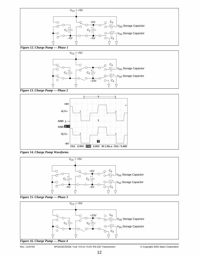
Phase 1— V
SS charge storage — During this phase of
the clock cycle, the positive side of capacitors C1
and C2 are initially charged to V
CC. C
l+ is then
switched to GND and the charge in C1
– is trans-ferred to C
2–. Since C
2+ is connected to V
CC, the
voltage potential across capacitor C2 is now 2
times VCC
.
Phase 2— V
SS transfer — Phase two of the clock con-
nects the negative terminal of C2 to the V
SS
storage capacitor and the positive terminal of C2
to GND. This transfers a negative generatedvoltage to C
3. This generated voltage is regu-
lated to a minimum voltage of -5.5V. Simulta-neous with the transfer of the voltage to C
3, the
positive side of capacitor C1 is switched to V
CC
and the negative side is connected to GND.
Phase 3— V
DD charge storage — The third phase of the
clock is identical to the first phase — the chargetransferred in C
1 produces –V
CC in the negative
terminal of C1, which is applied to the negative
side of capacitor C2. Since C
2+ is at V
CC, the
voltage potential across C2 is 2 times V
CC.
Table 2. Truth Table Logic for Shutdown and EnableControl
NDHS NE TUOxT TUOxR
0 0 etats-irT evitcA
0 1 etats-irT etats-irT
1 0 evitcA evitcA
1 1 evitcA etats-irT
11
Rev. 11/07/02 SP3222E/3232E True +3.0 to +5.0V RS-232 Transceivers © Copyright 2001 Sipex Corporation
Phase 4— V
DD transfer — The fourth phase of the clock
connects the negative terminal of C2 to GND,
and transfers this positive generated voltageacross C
2 to C
4, the V
DD storage capacitor. This
voltage is regulated to +5.5V. At this voltage,the internal oscillator is disabled. Simultaneouswith the transfer of the voltage to C
4, the positive
side of capacitor C1 is switched to V
CC and the
negative side is connected to GND, allowing thecharge pump cycle to begin again. The chargepump cycle will continue as long as the opera-tional conditions for the internal oscillator arepresent.
Since both V+ and V– are separately generatedfrom V
CC; in a no–load condition V+ and V– will
be symmetrical. Older charge pump approachesthat generate V– from V+ will show a decrease inthe magnitude of V– compared to V+ due to theinherent inefficiencies in the design.
The clock rate for the charge pump typicallyoperates at 250kHz. The external capacitors canbe as low as 0.1µF with a 16V breakdownvoltage rating.
ESD Tolerance
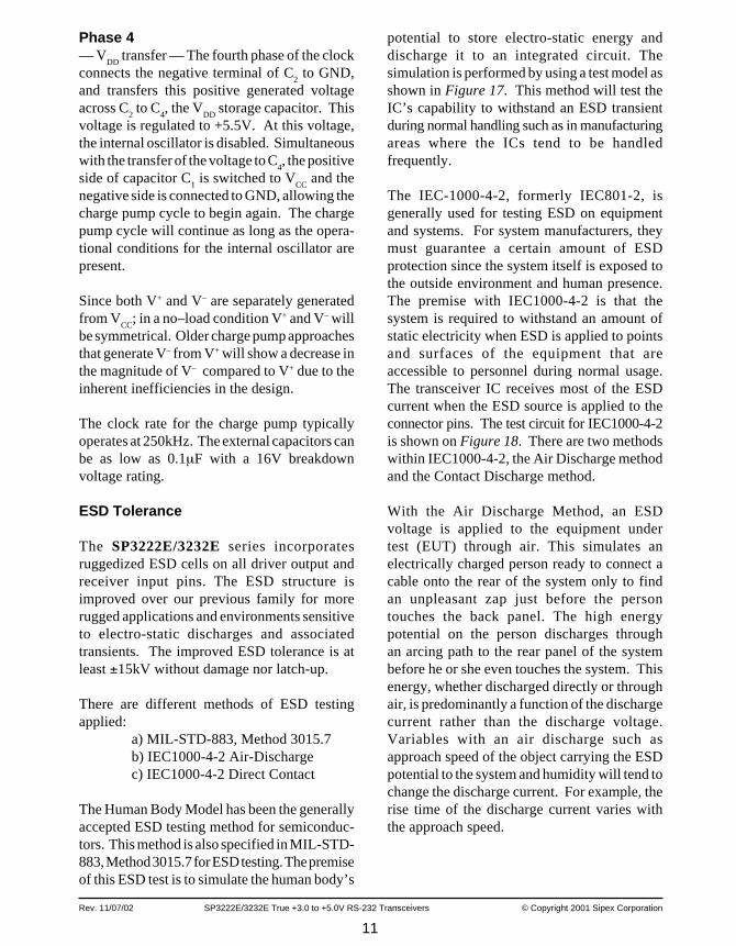
The SP3222E/3232E series incorporatesruggedized ESD cells on all driver output andreceiver input pins. The ESD structure isimproved over our previous family for morerugged applications and environments sensitiveto electro-static discharges and associatedtransients. The improved ESD tolerance is atleast ±15kV without damage nor latch-up.
There are different methods of ESD testingapplied:
a) MIL-STD-883, Method 3015.7b) IEC1000-4-2 Air-Dischargec) IEC1000-4-2 Direct Contact
The Human Body Model has been the generallyaccepted ESD testing method for semiconduc-tors. This method is also specified in MIL-STD-883, Method 3015.7 for ESD testing. The premiseof this ESD test is to simulate the human body’s
potential to store electro-static energy anddischarge it to an integrated circuit. Thesimulation is performed by using a test model asshown in Figure 17. This method will test theIC’s capability to withstand an ESD transientduring normal handling such as in manufacturingareas where the ICs tend to be handledfrequently.
The IEC-1000-4-2, formerly IEC801-2, isgenerally used for testing ESD on equipmentand systems. For system manufacturers, theymust guarantee a certain amount of ESDprotection since the system itself is exposed tothe outside environment and human presence.The premise with IEC1000-4-2 is that thesystem is required to withstand an amount ofstatic electricity when ESD is applied to pointsand surfaces of the equipment that areaccessible to personnel during normal usage.The transceiver IC receives most of the ESDcurrent when the ESD source is applied to theconnector pins. The test circuit for IEC1000-4-2is shown on Figure 18. There are two methodswithin IEC1000-4-2, the Air Discharge methodand the Contact Discharge method.
With the Air Discharge Method, an ESDvoltage is applied to the equipment undertest (EUT) through air. This simulates anelectrically charged person ready to connect acable onto the rear of the system only to findan unpleasant zap just before the persontouches the back panel. The high energypotential on the person discharges throughan arcing path to the rear panel of the systembefore he or she even touches the system. Thisenergy, whether discharged directly or throughair, is predominantly a function of the dischargecurrent rather than the discharge voltage.Variables with an air discharge such asapproach speed of the object carrying the ESDpotential to the system and humidity will tend tochange the discharge current. For example, therise time of the discharge current varies withthe approach speed.
Rev. 11/07/02 SP3222E/3232E True +3.0 to +5.0V RS-232 Transceivers © Copyright 2002 Sipex Corporation
12
VCC = +5V
–5V –5V
+5V
VSS Storage Capacitor
VDD Storage Capacitor
C1 C2
C3
C4+
+
+ +–
–––
Figure 12. Charge Pump — Phase 1
Figure 13. Charge Pump — Phase 2
VCC = +5V
–10V
VSS Storage Capacitor
VDD Storage Capacitor
C1 C2
C3
C4+
+
+ +–
–––
Figure 14. Charge Pump Waveforms
Figure 15. Charge Pump — Phase 3
VCC = +5V
–5V
+5V
–5V
VSS Storage Capacitor
VDD Storage Capacitor
C1 C2
C3
C4+
+
+ +–
–––
VCC = +5V
+10V
VSS Storage Capacitor
VDD Storage Capacitor
C1 C2
C3
C4+
+
+ +–
–––
Figure 16. Charge Pump — Phase 4
Ch1 2.00V Ch2 2.00V M 1.00µs Ch1 5.48V
2
1 T
T[ ]
T
+6V
a) C2+
b) C2-
GND
GND
-6V
13
Rev. 11/07/02 SP3222E/3232E True +3.0 to +5.0V RS-232 Transceivers © Copyright 2001 Sipex Corporation
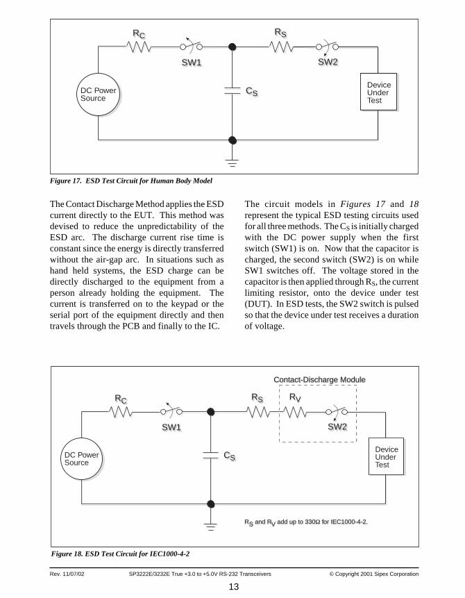
The Contact Discharge Method applies the ESDcurrent directly to the EUT. This method wasdevised to reduce the unpredictability of theESD arc. The discharge current rise time isconstant since the energy is directly transferredwithout the air-gap arc. In situations such ashand held systems, the ESD charge can bedirectly discharged to the equipment from aperson already holding the equipment. Thecurrent is transferred on to the keypad or theserial port of the equipment directly and thentravels through the PCB and finally to the IC.
The circuit models in Figures 17 and 18represent the typical ESD testing circuits usedfor all three methods. The CS is initially chargedwith the DC power supply when the firstswitch (SW1) is on. Now that the capacitor ischarged, the second switch (SW2) is on whileSW1 switches off. The voltage stored in thecapacitor is then applied through RS, the currentlimiting resistor, onto the device under test(DUT). In ESD tests, the SW2 switch is pulsedso that the device under test receives a durationof voltage.
RC
CS
RS
SW1 SW2
RC
DeviceUnderTest
DC PowerSource
CS
RS
SW1 SW2
Figure 17. ESD Test Circuit for Human Body Model
RS and RV add up to 330Ω for IEC1000-4-2.RS and RV add up to 330Ω for IEC1000-4-2.
Contact-Discharge Module
RVRC
CS
RS
SW1 SW2
RC
DeviceUnderTest
DC PowerSource
CS
RS
SW1 SW2
RV
Contact-Discharge Module
Figure 18. ESD Test Circuit for IEC1000-4-2
Rev. 11/07/02 SP3222E/3232E True +3.0 to +5.0V RS-232 Transceivers © Copyright 2002 Sipex Corporation
14
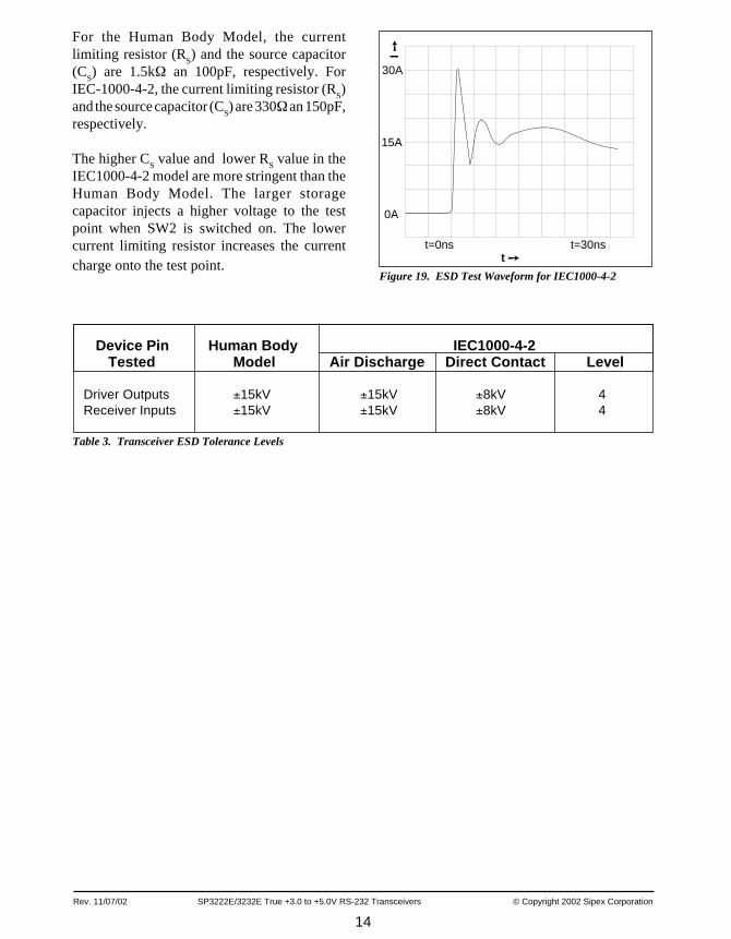
Figure 19. ESD Test Waveform for IEC1000-4-2
30A
I
0A
15A
t=30nst
t=0ns
For the Human Body Model, the currentlimiting resistor (R
S) and the source capacitor
(CS) are 1.5kΩ an 100pF, respectively. For
IEC-1000-4-2, the current limiting resistor (RS)
and the source capacitor (CS) are 330Ω an 150pF,
respectively.
The higher CS value and lower R
S value in the
IEC1000-4-2 model are more stringent than theHuman Body Model. The larger storagecapacitor injects a higher voltage to the testpoint when SW2 is switched on. The lowercurrent limiting resistor increases the currentcharge onto the test point.
Device Pin Human Body IEC1000-4-2 Tested Model Air Discharge Direct Contact Level
Driver Outputs ±15kV ±15kV ±8kV 4Receiver Inputs ±15kV ±15kV ±8kV 4
Table 3. Transceiver ESD Tolerance Levels
15
Rev. 11/07/02 SP3222E/3232E True +3.0 to +5.0V RS-232 Transceivers © Copyright 2001 Sipex Corporation
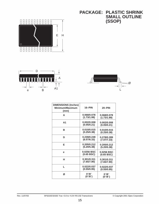
D
E H
PACKAGE: PLASTIC SHRINKSMALL OUTLINE(SSOP)
DIMENSIONS (Inches)Minimum/Maximum
(mm)20–PIN
A
A1
Ø
LBe
A
A1
B
D
E
e
H
L
Ø
0.068/0.078(1.73/1.99)
0.002/0.008(0.05/0.21)
0.010/0.015(0.25/0.38)
0.278/0.289(7.07/7.33)
0.205/0.212(5.20/5.38)
0.0256 BSC(0.65 BSC)
0.301/0.311(7.65/7.90)
0.022/0.037(0.55/0.95)
0°/8°(0°/8°)
16–PIN
0.068/0.078(1.73/1.99)
0.002/0.008(0.05/0.21)
0.010/0.015(0.25/0.38)
0.239/0.249(6.07/6.33)
0.205/0.212(5.20/5.38)
0.0256 BSC(0.65 BSC)
0.301/0.311(7.65/7.90)
0.022/0.037(0.55/0.95)
0°/8°(0°/8°)

Rev. 11/07/02 SP3222E/3232E True +3.0 to +5.0V RS-232 Transceivers © Copyright 2002 Sipex Corporation
16
D
ALTERNATEEND PINS
(BOTH ENDS)
D1 = 0.005" min.(0.127 min.)
E
PACKAGE: PLASTICDUAL–IN–LINE(NARROW)
A = 0.210" max.(5.334 max).
E1
CØL
A2
A1 = 0.015" min.(0.381min.)
BB1
e = 0.100 BSC(2.540 BSC)
eA = 0.300 BSC(7.620 BSC)
DIMENSIONS (Inches)Minimum/Maximum
(mm)
A2
B
B1
C
D
E
E1
L
Ø
16–PIN
0.115/0.195(2.921/4.953)
0.014/0.022(0.356/0.559)
0.045/0.070(1.143/1.778)
0.008/0.014(0.203/0.356)
0.780/0.800(19.812/20.320)
0.300/0.325(7.620/8.255)
0.240/0.280(6.096/7.112)
0.115/0.150(2.921/3.810)
0°/ 15°(0°/15°)
18–PIN
0.115/0.195(2.921/4.953)
0.014/0.022(0.356/0.559)
0.045/0.070(1.143/1.778)
0.008/0.014(0.203/0.356)
0.880/0.920(22.352/23.368)
0.300/0.325(7.620/8.255)
0.240/0.280(6.096/7.112)
0.115/0.150(2.921/3.810)
0°/ 15°(0°/15°)
17
Rev. 11/07/02 SP3222E/3232E True +3.0 to +5.0V RS-232 Transceivers © Copyright 2001 Sipex Corporation
D
E H
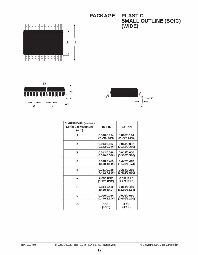
PACKAGE: PLASTICSMALL OUTLINE (SOIC)(WIDE)
DIMENSIONS (Inches)Minimum/Maximum
(mm)
A
A1
Ø
LBe
A
A1
B
D
E
e
H
L
Ø
16–PIN
0.090/0.104(2.29/2.649)
0.004/0.012(0.102/0.300)
0.013/0.020(0.330/0.508)
0.398/0.413(10.10/10.49)
0.291/0.299(7.402/7.600)
0.050 BSC(1.270 BSC)
0.394/0.419(10.00/10.64)
0.016/0.050(0.406/1.270)
0°/8°(0°/8°)
18–PIN
0.090/0.104(2.29/2.649))
0.004/0.012(0.102/0.300)
0.013/0.020(0.330/0.508)
0.447/0.463(11.35/11.74)
0.291/0.299(7.402/7.600)
0.050 BSC(1.270 BSC)
0.394/0.419(10.00/10.64)
0.016/0.050(0.406/1.270)
0°/8°(0°/8°)
Rev. 11/07/02 SP3222E/3232E True +3.0 to +5.0V RS-232 Transceivers © Copyright 2002 Sipex Corporation
18
D
E H
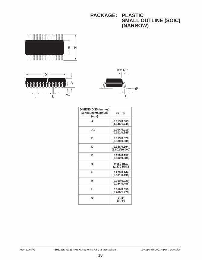
PACKAGE: PLASTICSMALL OUTLINE (SOIC)(NARROW)
DIMENSIONS (Inches)Minimum/Maximum
(mm)
A
A1
Ø
LBe
h x 45°
A
A1
B
D
E
e
H
h
L
Ø
16–PIN
0.053/0.069(1.346/1.748)
0.004/0.010(0.102/0.249)
0.013/0.020(0.330/0.508)
0.386/0.394(9.802/10.000)
0.150/0.157(3.802/3.988)
0.050 BSC(1.270 BSC)
0.228/0.244(5.801/6.198)
0.010/0.020(0.254/0.498)
0.016/0.050(0.406/1.270)
0°/8°(0°/8°)
19
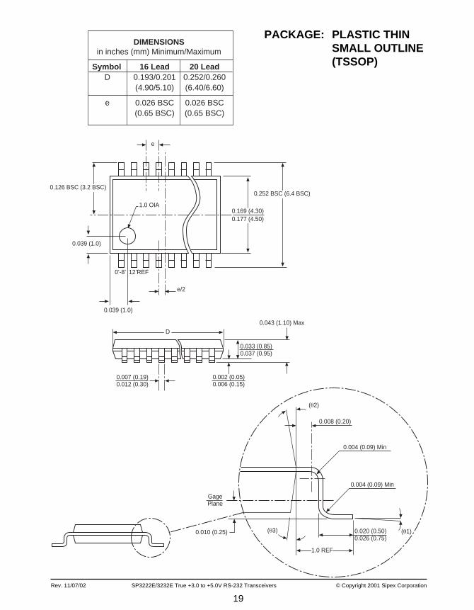
Rev. 11/07/02 SP3222E/3232E True +3.0 to +5.0V RS-232 Transceivers © Copyright 2001 Sipex Corporation
GagePlane
1.0 OIA
e
0.169 (4.30)0.177 (4.50)
0.252 BSC (6.4 BSC)
0’-8’ 12’REF
0.039 (1.0)
e/2
0.039 (1.0)
0.126 BSC (3.2 BSC)
D
0.007 (0.19)0.012 (0.30)
0.033 (0.85)0.037 (0.95)
0.002 (0.05)0.006 (0.15)
0.043 (1.10) Max
(θ3)
1.0 REF
0.020 (0.50)0.026 (0.75)
(θ1)
0.004 (0.09) Min
0.004 (0.09) Min
0.010 (0.25)
(θ2)
0.008 (0.20)
DIMENSIONSin inches (mm) Minimum/Maximum
Symbol 16 Lead 20 LeadD 0.193/0.201 0.252/0.260
(4.90/5.10) (6.40/6.60)
e 0.026 BSC 0.026 BSC(0.65 BSC) (0.65 BSC)
PACKAGE: PLASTIC THINSMALL OUTLINE(TSSOP)
Rev. 11/07/02 SP3222E/3232E True +3.0 to +5.0V RS-232 Transceivers © Copyright 2002 Sipex Corporation
20
ORDERING INFORMATIONModel Temperature Range Package TypeSP3222ECA ............................................. 0˚C to +70˚C .......................................... 20-Pin SSOPSP3222ECP ............................................. 0˚C to +70˚C ............................................ 18-Pin PDIPSP3222ECT ............................................. 0˚C to +70˚C ........................................ 18-Pin WSOICSP3222ECY ............................................. 0˚C to +70˚C ........................................ 20-Pin TSSOPSP3222EEA ............................................ -40˚C to +85˚C ........................................ 20-Pin SSOPSP3222EEP ............................................ -40˚C to +85˚C .......................................... 18-Pin PDIPSP3222EET ............................................ -40˚C to +85˚C ...................................... 18-Pin WSOICSP3222EEY ............................................ -40˚C to +85˚C ...................................... 20-Pin TSSOP
SP3232ECA ............................................. 0˚C to +70˚C .......................................... 16-Pin SSOPSP3232ECP ............................................. 0˚C to +70˚C ............................................ 16-Pin PDIPSP3232ECT ............................................. 0˚C to +70˚C ........................................ 16-Pin WSOICSP3232ECN ............................................. 0˚C to +70˚C ......................................... 16-Pin nSOICSP3232ECY ............................................. 0˚C to +70˚C ........................................ 16-Pin TSSOPSP3232EEA ............................................ -40˚C to +85˚C ........................................ 16-Pin SSOPSP3232EEP ............................................ -40˚C to +85˚C .......................................... 16-Pin PDIPSP3232EET ............................................ -40˚C to +85˚C ...................................... 16-Pin WSOICSP3232EEN ............................................ -40˚C to +85˚C ....................................... 16-Pin nSOICSP3232EEY ............................................ -40˚C to +85˚C ...................................... 16-Pin TSSOP
Corporation
SIGNAL PROCESSING EXCELLENCE
Sipex Corporation reserves the right to make changes to any products described herein. Sipex does not assume any liability arising out of theapplication or use of any product or circuit described hereing; neither does it convey any license under its patent rights nor the rights of others.
Sipex Corporation
Headquarters andSales Office22 Linnell CircleBillerica, MA 01821TEL: (978) 667-8700FAX: (978) 670-9001e-mail: [email protected]
Sales Office233 South Hillview DriveMilpitas, CA 95035TEL: (408) 934-7500FAX: (408) 935-7600
Please consult the factory for pricing and availability on a Tape-On-Reel option.

This datasheet has been download from:
www.datasheetcatalog.com
Datasheets for electronics components.
Related Documents