Troubleshooting Coherent Optical Communication Systems Created by: Michael Koenigsmann Application Specialist Digital & Photonic Test Division May 18 th 2015 © 2015 Keysight Technologies Presented by: Rodrigo Vicentini Applications Engineering Manager Latin America Region

Welcome message from author
This document is posted to help you gain knowledge. Please leave a comment to let me know what you think about it! Share it to your friends and learn new things together.
Transcript

Troubleshooting Coherent Optical Communication Systems
Created by:Michael KoenigsmannApplication SpecialistDigital & Photonic Test Division
May 18th 2015
© 2015 Keysight Technologies
Presented by:Rodrigo VicentiniApplications Engineering ManagerLatin America Region

Agenda
• Market and Technology Trends
• Coherent Measurement Challenges
• Typical Tests in Coherent Transmission Systems
• Typical Impairment Emulation in the electrical Domain
• Tools to generate signals for Coherent Optical Applications
• References

Market and Technology Trends
Drivers for higher Datarates

Page 4
Troubleshooting Coherent Optical Comms Systems
Market and Technology TrendsBig Data Demand drives Technology Changes
Challenges:• Transmission demand exceeds system capacity• Cost-effective increase of capacity • Pressure to release new technology on time
To maximize transmission within Phy layer, combine & optimize all dimensions for efficiency, cost, power, reach, reliabiliy etc.
• Mobile apps and services, • high resolution devices, • Internet of Things
drive
high speed I/O, network and data center traffic
Modulation
Sym
bo
l Rat
e
Multi level signaling
in digital links,
e.g. C-Phy, PAMx
Parallel lines, subcarrier density
Polarization Mux, OFDM, DMT
Amplitude & Phase
modulation in optical links
e.g. QPSK, QAMx
Maximize Bits per Symbol
Increase Symbol Rate
32 GBd and beyond
Nyquist fs > 2 x fmax
Rule of thumb:
sampling rate = 2.5x Signal BW
Maximize # of carriersBy 2020 there will be around 20 Billion
devices connected to the Internet
© 2015 Keysight Technologies

Page
Maximize Transmission within Physical Layer
Troubleshooting Coherent Optical Comms Systems
Different techniques…
Motivation
Higher Order Modulation Formats OFDM
From OOK to Coherent Detection
Time-Domain Pulse Shaping
Polarization Division Multiplex
4
© 2015 Keysight Technologies

Page
Application Requirements
Troubleshooting Coherent Optical Comms Systems 6
Coherent Optical Communication
• Requirements for a test instrument:• Flexibilty to address different modulation schemes• Clean signal to test your device and not your instrument• Bandwidth at least 20 GHz• 4 sychronized channels to support dual polarization (= 2 pairs of I/Q signal)
QPSK QAM128 OFDM
Need higher data throughput: 100 G 400 G 1 Tbit/s
© 2015 Keysight Technologies

Page
Emulate Optical Distortions in the Electrical Space
7
Pattern Gen
RefTx or golden
Line Card
Error Detector
Network or Test Bed
DUT (100/400G
Rx)
AWG DUT (DSP)
ADC
ADC
ADC
ADC
Digital Coherent Receiver DSP Test
Error Detector
DUT (100/400G
Tx)AWG
- or -
Traditional setup
Test setup with AWG
Deterministic and precise testing with complex impairmentse.g. Phase Noise, OSNR, Polarization, PMD
Troubleshooting Coherent Optical Comms Systems
OSNR Gen.
DUT (100/400G
Rx)AWG Error
DetectorE/O
- or -
© 2015 Keysight Technologies

Page
AWG’s in Coherent Optical Applications
– Endless modulation formats for higher data throughput
– Generates clean signals at 32 GBd and beyond
– Provides 4 independent analog outputs for dual-polarization optical applications
• Uses out of the box and in-situ calibration to achieve a clean signal at the device under test
• Emulate optical distortions in the electrical space
8
Cost-effective increase in capacity
16 QAM at 32 GBd with < 4% EVM
QPSK Signalwith addedphase noise;emulating a2 MHz laserline width
Troubleshooting Coherent Optical Comms Systems
Optical Modulation
Generator TooI
© 2015 Keysight Technologies

Coherent Measurement Challenges
• Clean Signal generation (electrical & optical)• Clean Signal at defined test points• High datarates 32 GBd and beyond• Accurate and Repeatable Test Signals• Distortion Emulation• Flexible Modulation Formats

Page
Accurate and Repeatable Test Results
Out-of-the-box calibration ensures clean signal at the frontpanel connector
In-situ calibration – extend clean signal to the receiver test point
• S-Parameters of channel are embedded or de-embedded
• Frequency/Phase response is measured in-system andthen de-embedded
11
QPSK, 32 GBd PRBS 6 Gbit/s
Without correction With correction Without correction With correction
Troubleshooting Coherent Optical Comms Systems
© 2015 Keysight Technologies
Page
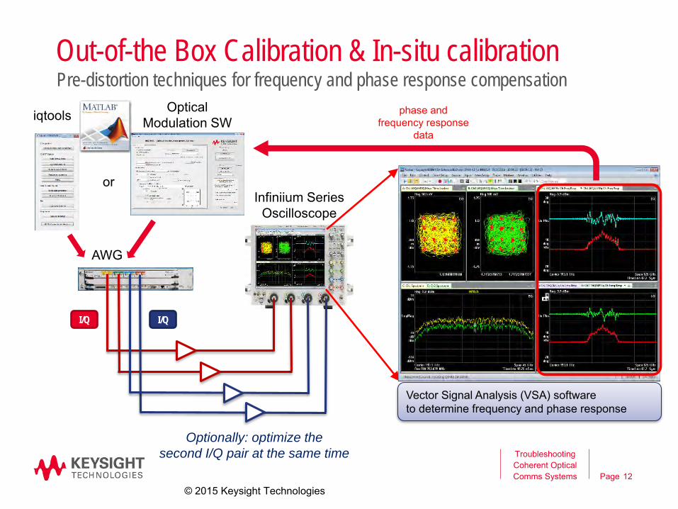
Out-of-the Box Calibration & In-situ calibrationPre-distortion techniques for frequency and phase response compensation
12
AWG
Optionally: optimize the
second I/Q pair at the same time Troubleshooting Coherent Optical Comms Systems
or
iqtools Optical Modulation SW
phase and frequency response
data
I/Q I/Q
Vector Signal Analysis (VSA) softwareto determine frequency and phase response
Infiniium SeriesOscilloscope
© 2015 Keysight Technologies

Page
In-situ-calibration
13
End-to-end equalization
Measure frequency/phase response as determined by the coherent receiver End-to-end calibration of the whole transmission system This includes the characteristic of the receiver as well !
Troubleshooting Coherent Optical Comms Systems
M8195A
I
Y-Polarization
Q
I
Q
X-Polarization
π/2
π/2
Tunable Laser
N4391A or N4392A
AWGMZMAmplifiers
Coherent Receiver
Optional Fiber & Optical Amplifiers
Optical ModulationGenerator Tool phase and
frequency response data
© 2015 Keysight Technologies

Typical Tests inCoherent Transmissions
© 2015 Keysight Technologies

Page 15
Test application: system and link stress test
TXelectronic
IQMod.
CarrierLaser
ROADMWSS
OpticalCoherent IQ det.
RXSignal
Processing
LOLaser
Typical test requirements: BER (EVM) vs. Power or OSNR Spectral behavior over 1-2 neighbor channels Signal integrity along the link (time domain modulation analysis) Nonlinear characteristics (PMD, PDL, CD,…)
N4391A or N4392A
Troubleshooting Coherent Optical Comms Systems
15
ROADM – Reconfigurable Optical Add-Drop MultiplexerWSS - Wavelength Selective Switching
© 2015 Keysight Technologies

Page 16
Test application: Rx stress test (optical)
Multi-format Reference Transmitter oroptical AWG with or without stress generation
M8195A + OMFT + Tunable Laser+ Optical Modulation Gen. Tool
OpticalCoherent IQ det.
RXSignal
Processing
LOLaser
Stress generationon Optical Signal- Loss- Polarization - PMD- OSNR- Non-Linearities
Troubleshooting Coherent Optical Comms Systems
16© 2015 Keysight Technologies
Typical requirements: Availability of numerous modulation formats for research and development High quality PAMx, (D)QPSK and QAMx signal for manufacturing Arbitrary constellations for advanced research required (arbitrary stress) BER vs various stress parameters Some customers need RZ DQPSK Support of up to 56 GBd rates for >> 100G research PRBS test pattern, Pre-defined or User-defined Test of receiver algorithm robustness with distorted signals

Page 17
Test application: Rx stress test (electrical)
Typical requirements: Availability of numerous modulation formats for research and development High quality PAMx, (D)QPSK and QAMx signal for manufacturing Arbitrary constellations for advanced research required (arbitrary stress) BER vs various stress parameters Some customers need RZ DQPSK Support of up to 56 GBd rates for >> 100G research PRBS test pattern, Pre-defined or User-defined Test of receiver algorithm robustness with distorted signals
Multi-format Reference Transmitter oroptical AWG with or without stress generation
M8195A + OMFT + Tunable Laser+ Optical Modulation Gen. Tool
OpticalCoherent IQ det.
RXSignal
Processing
LOLaser
Stress generationon Optical Signal- Loss- Polarization - PMD- OSNR- Non-Linearities
Stress generationon Electrical Signal- Loss- Polarization - PMD- OSNR- Non-Linearities
Troubleshooting Coherent Optical Comms Systems
17
M8195A + Optical Modulation Gen. Tool
© 2015 Keysight Technologies

Page 18
Test application: IQ modulator
Typical test requirements: Cut-off frequency for each path In-application test to specify best EVM and other measures Polarization behavior Phase Response, Skew Modulator Bias Control
Multiformat TXDAC electrical output !
Analysis ofmodulation quality andpolarization behaviour
Frequency responseof modulator
TXelectronic
IQMod.
CarrierLaser
I
Y-Polarization
Q
I
Q
X-Polarization
π/2
π/2
TunableLaser
M8195A + Tunable Laser+ Optical Modulation Gen. Tool
LCA
N4391A or N4392A
Troubleshooting Coherent Optical Comms Systems
18© 2015 Keysight Technologies

Page
Troubleshooting Coherent Optical Comms Systems 19
Typical Measures IndicationEVM & Q-Factor General figure of merit for Signal Quality
EVM percentile Signal Quality w/o the effect of IQ Gain Imbalance and Quadrature Error
IQ Gain Imbalance Different amplitudes for I- and Q-Signal
IQ Skew Timing skews between I- & Q-Signal
IQ Offset Wrong bias setting or DC offset at modulator
Quadrature Error IQ phase shifter, wrong bias point of 90 º phaseshifter
Frequency Error Carrier Frequency Offset between Tx & Rx, EVM
Symbol Rate Error, V-shape in ErrorVector vs Time Mismatch in Symbol Rate between Tx and Rx
Dual Pol: IQ Skews, X-Y Skew & X-Y Imbalance Skew & Gain differences between Polarizations
Bit Error Results Indentify Bit Errors per Polarization or acrossPolarization
Missing Transitions in Constellation De-correlation issue between I- & Q-Signal
Coherent testingTypical Measures
© 2015 Keysight Technologies

Page
EVM & Q-Factor
20
Troubleshooting Coherent Optical Comms Systems
Error Vectorconnects the measuredVector and the expectedvector, Error VectorMagnitude or EVM is magnitude of this vector
EVM Q-factor1% ~ 100
2% ~ 50
5% ~ 20
10% ~ 10
The Q-Factor describes the signal-to-noise ratio at the decision points. It is calculated from the EVM. The formula is proportional to 1/EVMa and the result is converted into dB. It is calculated from the Eye-Diagram
aEVM
1Q
© 2015 Keysight Technologies

Page
EVM percentile
21
Troubleshooting Coherent Optical Comms Systems
EVM_pctlEVM_pctl defines the radius of a circle around a group of measured constellation points centered at the reference constellation point.In contrast to EVM_pctl, the classical EVM value from the VSA software includes I-Q Imbalance and Quadrature Error and is a RMS averaged value. The “Hit Ratio” multiplied with the number of points is equal to the number of points outside the circle. For Gaussian Noise dominated impairments, the classical EVM and the EVM_pctl are equal if a “Hit Ratio” of 0.3173 is selected. The "Hit Ratio" can be set in the EVM_percentile algorithm of the OMA Software.
© 2015 Keysight Technologies
ConstellationReference
EVM_pctl
Page
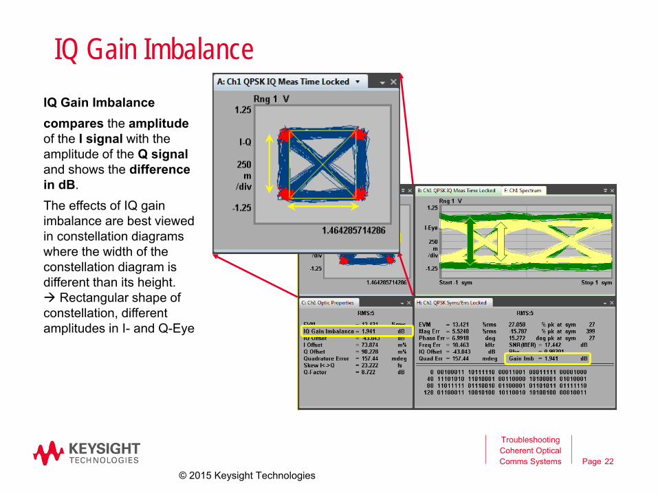
IQ Gain Imbalance
22
Troubleshooting Coherent Optical Comms Systems
IQ Gain Imbalancecompares the amplitudeof the I signal with the amplitude of the Q signal and shows the difference in dB.The effects of IQ gain imbalance are best viewed in constellation diagrams where the width of the constellation diagram is different than its height. Rectangular shape of constellation, different amplitudes in I- and Q-Eye
© 2015 Keysight Technologies

Page
IQ Skew
23
Troubleshooting Coherent Optical Comms Systems
IQ SkewTiming skew betweenI- and Q-signals distorted IQ Plot, Eye-
Diagrams are shiftedwith respect to eachother
45° transitions open up Increased EVM
© 2015 Keysight Technologies

Page
IQ Offset
24
Troubleshooting Coherent Optical Comms Systems
IQ OffsetDC offsets at the I- or the Q-Signals cause I/Q or origin offsets as shown. I/Q offsets can also resultin carrier feedthrough.It is a measure for the shift between the origin of the measured constellation with regard to the origin of the reference constellation (yellow).Without DC offsets, the carrier feed through as well as the IQ offset becomes zero (-infinity dB). Vertically shifted Eye-
Diagram traces Carrier Feedthrough EVM
carrier feed through
Individual I- and Q-
Imbalance available
© 2015 Keysight Technologies

Page
Quadrature Error
25
Troubleshooting Coherent Optical Comms Systems
Quadrature Errorindicates the orthogonal
error between the I and Q Quadrature-Phase. Ideally, I and Q should be orthogonal (90 degrees apart). In the screenshot to the right a quadrature error of 22.91 degrees means I and Q are 67,09degrees apart instead of 90 degrees.This could result from wrong bias point setting for the 90° phase shifter in the Mach-Zehnder-Modulator distorted IQ Plot,
distorted Eye-diagrams EVM
π/2
I
Q
© 2015 Keysight Technologies

Page
Frequency Error
26
Troubleshooting Coherent Optical Comms Systems
Frequency Errorshows the carrier's frequency error relative to the VSA's center frequency displayed in Hertz. It is the amount of frequency shift from the VSA's center frequency that the VSA must perform to achieve carrier lock. The maximum allowable Frequency Error depends on the Modulation Format used. Here’s a list of formats:
2 GHz
Modulation Format Maximum frequency offsetQPSK 9.6% symbol rate
16-QAM 4.8% symbol rate
32-QAM 3.15% symbol rate
64-QAM 4.65% symbol rate
128-QAM 0.3% symbol rate
256-QAM 0.3% symbol rate
512-QAM 0.15% symbol rate
1024-QAM 0.15% symbol rate
2048-QAM 0.1% symbol rate*
4096-QAM 0.1% symbol rate*
© 2015 Keysight Technologies

Page
Symbol Rate Error
27
Troubleshooting Coherent Optical Comms Systems
Symbol Rate ErrorIf the Digital Demodulator is only able to recover the clock phase but not the clock rate, a wrongsymbol rate shows up as typical „V“ shape whenlooking at EVM vs timeplot. Symbols start to spreadall over the constellation High EVM
Measured SymbolRate ≠SymbolRate setting
© 2015 Keysight Technologies

Page
Dual Pol: IQ Skews, XY Skew and XY Imbalance
28
Troubleshooting Coherent Optical Comms Systems
Optical Signal Summary ScreenDisplay of- Timing skew betweenI- and Q-Signals for X-and Y-Polarization- Timing skew betweenX- and Y-Polarization. - Gain Imbalance between X and YPolarization- Symbol Rate Display- Frequency Error between Tx and Rx (in this case OMA)- EVM and Q-Factor
© 2015 Keysight Technologies

Page
Bit Error Results
29
Troubleshooting Coherent Optical Comms Systems
Bit Error Result Screen- Actual BER- Cumulated BER - BER (EVM)- Bit & Error Counts- Delay between X & Y- PRBS generation details
© 2015 Keysight Technologies

Page
PRBS Pattern Sources
30
Troubleshooting Coherent Optical Comms Systems
Effects of IQ PRBS Delay in bit (PRBS length 215-1)
0 bit
2 bit
4 bit
1 bit
3 bit
5 bit
Effects of Delay issues between I- & Q-Data Source
Effect of PRBS delayUsing the same PRBS sequence for I and Q and decorrelating it with a toosmall delay might lead to missing transitions and asymetric spectralcontent !Screenshots were takenbased on a PRBS 215-1with different delaysbetween I and Q showingresult in the correspondingconstellation and spectrum.
© 2015 Keysight Technologies

Typical Impairment Emulation in the electrical Domain

Page
Example Impairment
Troubleshooting Coherent Optical Comms Systems 32
Phase Noise in Optical Modulation Generator Tool
© 2015 Keysight Technologies
Page
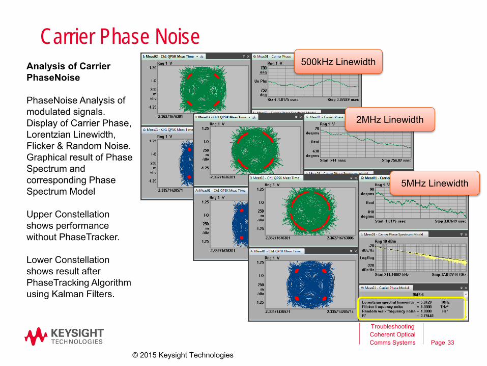
Carrier Phase Noise
33
Troubleshooting Coherent Optical Comms Systems
Analysis of Carrier PhaseNoise
PhaseNoise Analysis of modulated signals.Display of Carrier Phase,Lorentzian Linewidth, Flicker & Random Noise.Graphical result of Phase Spectrum and corresponding Phase Spectrum Model
Upper Constellationshows performancewithout PhaseTracker.
Lower Constellationshows result after PhaseTracking Algorithmusing Kalman Filters.
500kHz Linewidth
2MHz Linewidth
5MHz Linewidth
© 2015 Keysight Technologies

Page
Emulation of PolController
34
Troubleshooting Coherent Optical Comms Systems
Polarization Pattern: Great Circle
© 2015 Keysight Technologies

Page
Emulation of PolController
35
Troubleshooting Coherent Optical Comms Systems
Polarization Pattern: Slicer
© 2015 Keysight Technologies

Page
Stokes Space Analysis in OMA: Great Circle & Slicer
36
Troubleshooting Coherent Optical Comms Systems
Analysis of Stokes Space Trajectory
The OMA allows to analyzepolarization changes. Two patterns„Great Circle“ and „Slicer“ are generated with the AWG electrically. This electrical signal can be used for receiver stress testing.Here the electrical signal is directlyconnected to the OMA inputs.
Great Circle Slicer
© 2015 Keysight Technologies

Page 37
35ps PMD, 991ps^2 SOPMD
Troubleshooting Coherent Optical Comms Systems
Example Impairment: PMD (1st and 2nd order)PMD in Optical Modulation Generator Tool
© 2015 Keysight Technologies

Page
Example Impairment: PMD (1st and 2nd order)
38
Troubleshooting Coherent Optical Comms Systems
PMD Analysis in OMA
The OMA allows to compensate and analyze the PMD.An electrical signal is generated with the AWG and analyzed by the OMA.This signal could beused for receiver stress testing.
© 2015 Keysight Technologies

Tools to generate signals for Coherent Optical Applications
© 2015 Keysight Technologies
Page
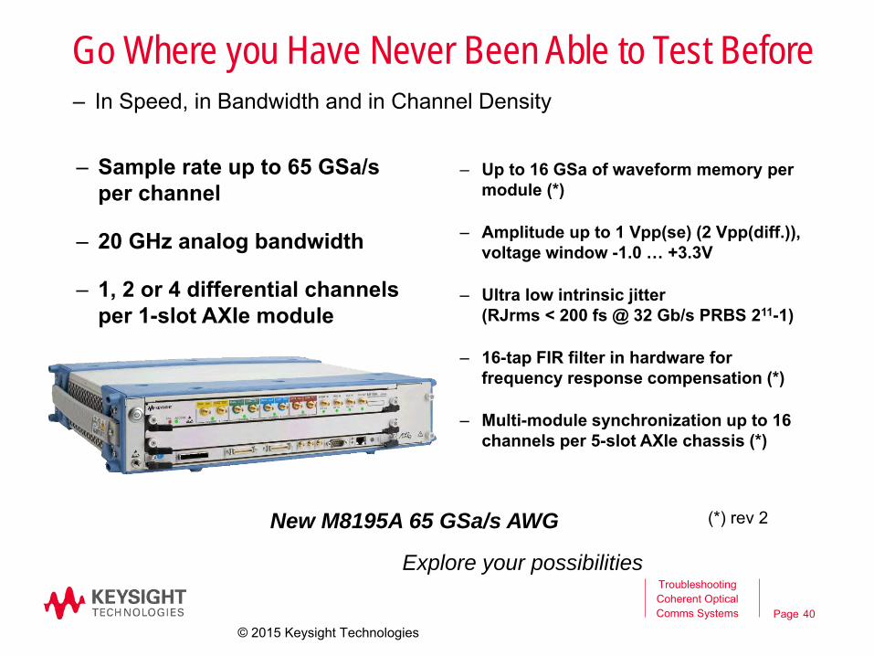
Go Where you Have Never Been Able to Test Before
– Sample rate up to 65 GSa/s per channel
– 20 GHz analog bandwidth
– 1, 2 or 4 differential channels per 1-slot AXIe module
– In Speed, in Bandwidth and in Channel Density
Explore your possibilities
New M8195A 65 GSa/s AWG
– Up to 16 GSa of waveform memory per module (*)
– Amplitude up to 1 Vpp(se) (2 Vpp(diff.)), voltage window -1.0 … +3.3V
– Ultra low intrinsic jitter(RJrms < 200 fs @ 32 Gb/s PRBS 211-1)
– 16-tap FIR filter in hardware for frequency response compensation (*)
– Multi-module synchronization up to 16 channels per 5-slot AXIe chassis (*)
(*) rev 2
40
Troubleshooting Coherent Optical Comms Systems
© 2015 Keysight Technologies
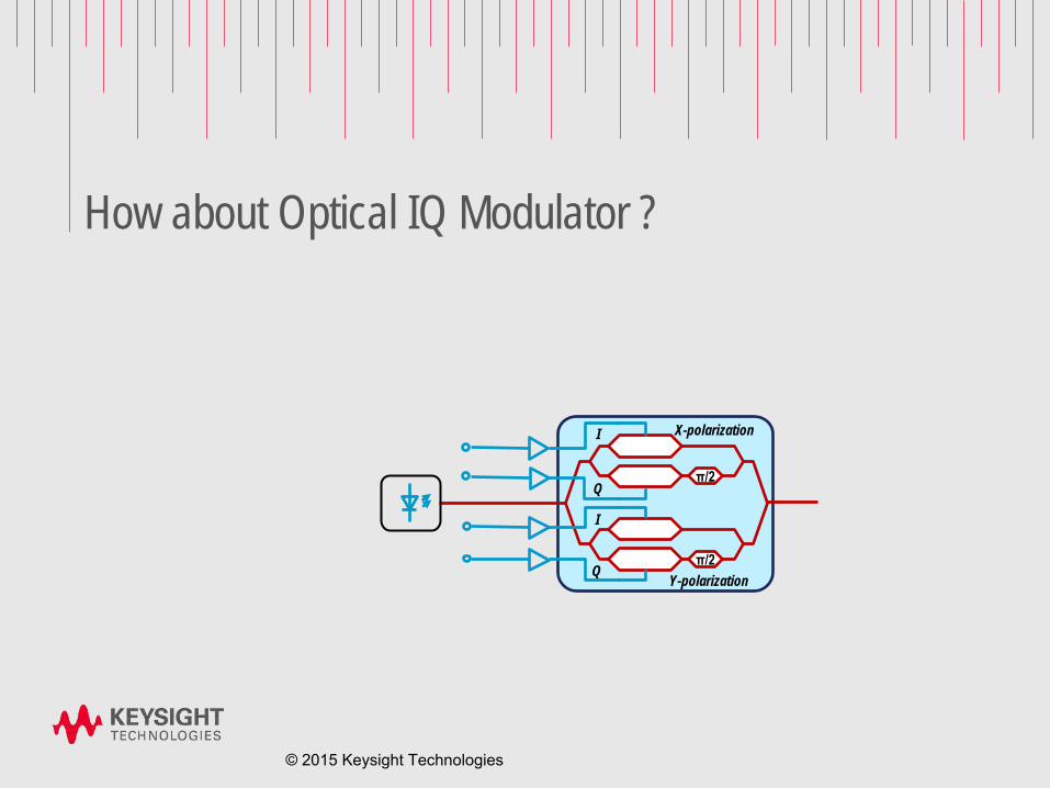
How about Optical IQ Modulator ?
I
Y-polarization
Q
I
Q
X-polarization
π/2
π/2
© 2015 Keysight Technologies

Page
Optical IQ Modulator:
Troubleshooting Coherent Optical Comms Systems 42
Optical Multiformat Transmitter: OMFT by IDPhotonics / HHI
• Symbol rate 46 GBd for binary formats such as
BPSK, QPSK 34 GBd: for multi-level formats
such as 16QAM • typically >23 GHz BW Dual polarization I-Q modulator
with typically 28 GHz bandwidth 40 GHz linear RF amplifiers
• C+L band• Manual as well as automatic bias
setting (automatic for QPSK and 16-QAM only)
• In combination with DAC/AWG:pre-distortion to compensate for nonlinearities of amplifiers and modulator
• 19“ form factor
OMFT frequency response (S-parameters) and RF cables de-embedded in AWG
In combination with M8195A AWG
© 2015 Keysight Technologies
OMFT performance verified in combinationwith M8195A AWG
Page
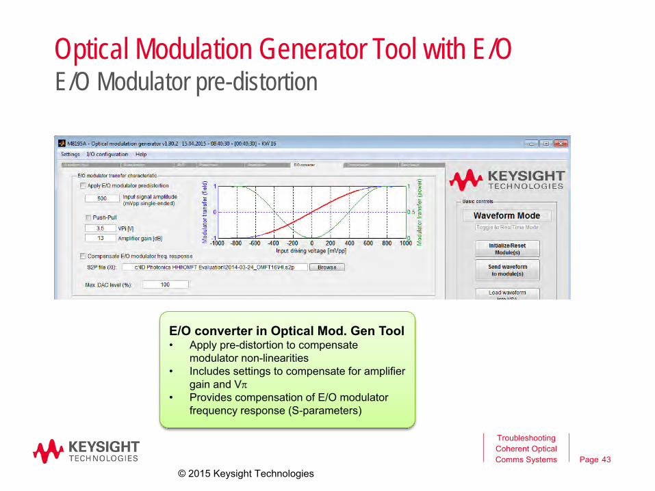
Optical Modulation Generator Tool with E/O
Troubleshooting Coherent Optical Comms Systems 43
E/O Modulator pre-distortion
E/O converter in Optical Mod. Gen Tool• Apply pre-distortion to compensate
modulator non-linearities• Includes settings to compensate for amplifier
gain and Vp• Provides compensation of E/O modulator
frequency response (S-parameters)
© 2015 Keysight Technologies

Page
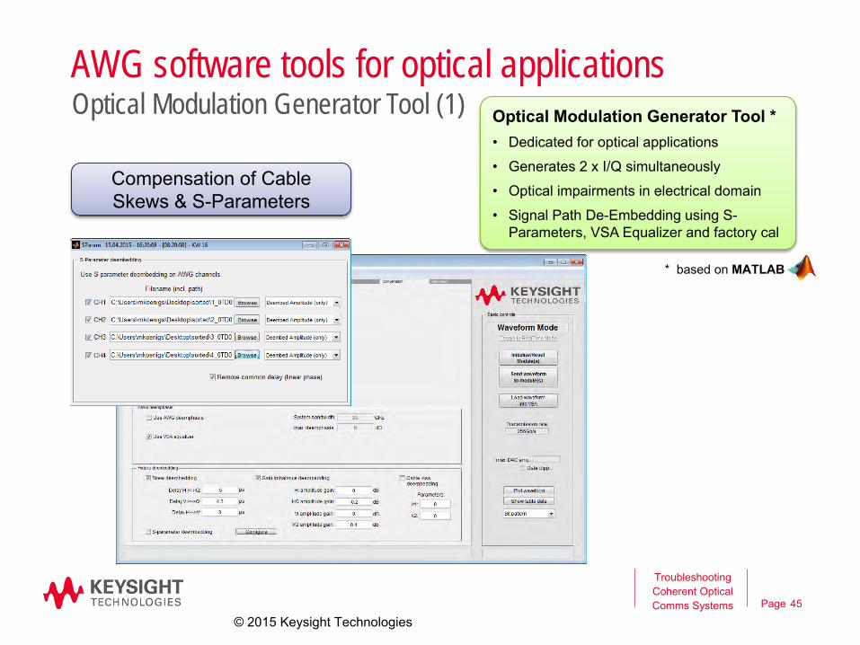
AWG software tools for optical applications
44
Troubleshooting Coherent Optical Comms Systems
Optical Modulation Generator Tool *• Dedicated for optical applications
• Generates 2 x I/Q simultaneously
• Optical impairments in electrical domain
• Signal Path De-Embedding using S-Parameters, VSA Equalizer and factory cal
* based on MATLAB
Optical Modulation Generator Tool (1)
© 2015 Keysight Technologies
Waveform Input page
Basic Setup Amplitude
Pulse Shaping
Page
AWG software tools for optical applications
45
Troubleshooting Coherent Optical Comms Systems
Optical Modulation Generator Tool *• Dedicated for optical applications
• Generates 2 x I/Q simultaneously
• Optical impairments in electrical domain
• Signal Path De-Embedding using S-Parameters, VSA Equalizer and factory cal
* based on MATLAB
Optical Modulation Generator Tool (1)
Compensation of Cable Skews & S-Parameters
© 2015 Keysight Technologies

Page
AWG software tools for optical applications
46
Troubleshooting Coherent Optical Comms Systems
* based on MATLAB
Optical Modulation Generator Tool (2) Optical Modulation Generator Tool *Electrical Emulation of Optical Signal Properties in Real Time (1):
- Phase Noise & Laser Linewidth
- Polarization Rotation
- 1st & 2nd order PMD
(1) with Rev 2 of AWGin Oct 2015
© 2015 Keysight Technologies
Polarization
Phase Noise
PMD

Tools for Coherent Signal Analysis

Page
N439xA Optical Modulation Analyzer Family
N4391A Optical Modulation Analyzer• 4 x 33 GHz in a single scope• 4 x 63 GHz as dual instrument
setup special (call factory)• 4 x 80 GSa/s sampling rate (160 Gsa/s for 63 GHz) • Up to 2 GSa/Ch memory• Lowest noise floor (typ. 1.5% EVMrms)
Troubleshooting Coherent Optical Comms Systems 48
For coherent transmission research & Mfg
N4392A integrated Optical Mod. Analyzer• Compact, fully integrated, no external cabling• 4 x 23 GHz in a single instrument for dual
polarization optical analysis• 4 x 23 GHz electrical inputs for dual polarization
ICR testing• 4 x 63 GSa/s sampling rate • 16 kSa/Ch memory• Noise floor (typ. 2 % EVMrms)
© 2015 Keysight Technologies

Page
Smart Setup in OMA Software
Troubleshooting Coherent Optical Comms Systems 49
„Smart setup“ - the easiest way to setup an OMA
0 Enter carrier wavelength or frequencyEnter symbol rateCheck modulation formatSelect between back to back and link measurement
-> done
1
2
3
4
1234
© 2015 Keysight Technologies

Page
Tabular Measurement results, well structured
Troubleshooting Coherent Optical Comms Systems 50
Per Polarization results Cross Channel results
X-Polarization
Y-Polarization
© 2015 Keysight Technologies
Page
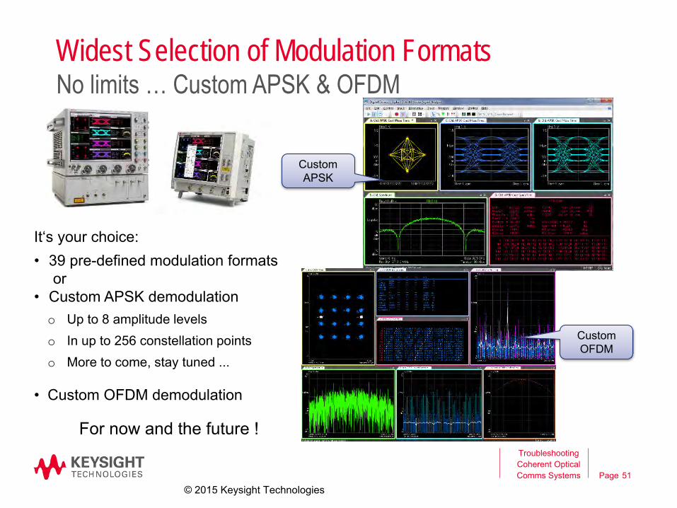
Widest Selection of Modulation Formats
Troubleshooting Coherent Optical Comms Systems 51
No limits … Custom APSK & OFDM
It‘s your choice:• 39 pre-defined modulation formats
or• Custom APSK demodulation
o Up to 8 amplitude levelso In up to 256 constellation pointso More to come, stay tuned ...
• Custom OFDM demodulation
For now and the future !
© 2015 Keysight Technologies
Custom APSK
Custom OFDM

Page
Summary Optical Communication Solutions
52
Keysight’s Offering
Wideband AWG
Tools for Coherent Signal Generation
Accurate and Repeatable Impairments
Tools for Coherent Signal Analysis
Troubleshooting Coherent Optical Comms Systems
N4391A OMA
M8195A AWG
Opt.Mod.Gen.Tool
© 2015 Keysight Technologies

Page
Further References
53
Troubleshooting Coherent Optical Comms Systems
Publication title Publication No.N4391A Optical Modulation Analyzer – Data Sheet 5990-3509ENN4392A Integrated Optical Modulation Analyzer – Data Sheet 5990-9863ENInfiniium Z-Series Oscilloscopes - Data Sheet 5991-3868ENM8195A 65 GSa/s Arbitrary Waveform Generator 5992-0014EN
Metrology of Advanced Optical Modulation Formats - White Paper 5990-3748ENKalman Filter Based Estimation and Demodulation of Complex Signals – White paper 5990-6409EN
Vector Signal Analysis Basics - Application Note 5989-1121ENDigital Modulation in Communications Systems - An Introduction – Application Note 5965-7160EEssentials of Coherent Optical Data Transmission - Application Note 5991-1809EN
Contact: [email protected]
More Information is available from these Jumpstations:Arbitrary Waveform Generator M8195A andOptical Modulation Generator Software: www.keysight.com/find/M8195AOptical Modulation Analyzer: www.keysight.com/find/OMALightwave Component Analyzer: www.keysight.com/find/LCA
© 2015 Keysight Technologies

Questions?
Comments?
54
Troubleshooting Coherent Optical Comms Systems

Page
Troubleshooting Coherent Optical Comms Systems 55

Backup

Page
Overview: AWG Software tools for coherent optical applications
Soft Front PanelOptical
ModulationSoftware
IQTools
Availability Comes with M8195A Firmware
Purchased separately
Available free of charge
Requires - MATLAB runtime
Modulation Formats
QPSK, QAMx andmany more QPSK, QAMx QPSK, QAMx,
OFDM
Dual I/Q Yes Yes No
Built-in Cal Yes Yes Yes
In-system Cal Manual Automatic 1, 2 Automatic 1, 2, 3
I/Q Skew Manual Manual Automatic
Optical impairments
(incl. support for real-time DSP)
No Yes No
1 Keysight Infiniium Series Scope needed 2 using VSA Equalizer 3 using own cal routine
MATLAB
Troubleshooting Coherent Optical Comms Systems 57
© 2015 Keysight Technologies

Page
N4391A & N4392A core specification comparison
Troubleshooting Coherent Optical Comms Systems 58
Parameter N4391A N4392AAnalog Bandwidth 4x 33 GHz 4x 23 GHzEVM noise floor typ. 1) < 1.5 % rms < 2 % rmsSample rate 4x 80 GSa/s 4x 63 GSa/sMax. BaudRate 63 GBd 46 GBdSensitivity -20 dBm -22 dBmSample Memory Up to 4x 2 GSa 4x 16 kSaSoftware platform VSA/OMA 4.xWavelength accuracy +/- 5 pm +/- 2 pmWeight ~ 48 kg (106 lbs) 13 kg (28.7 lbs)Portability no yes
1) @ reference conditions
© 2015 Keysight Technologies

Page
Debug your Tx by identifiyingthe path of each data stream
Full flexibility to setup the link from pattern source to tributary
Select Pre-defined orUser PRBS files
Easy intuitive setup
Individual BER Test on each Tributary
Troubleshooting Coherent Optical Comms Systems 59
Debug your transmitter faster
© 2015 Keysight Technologies

Page
New Measurements and Result Tables
Troubleshooting Coherent Optical Comms Systems 60
7 new measurement traces and tables related to eachpolarization plane
4 new measurement traces and tables for cross-channelmeasurement results
Get new measurement results in the same way as you are used to.
© 2015 Keysight Technologies

Page
Improved Training Tools
Troubleshooting Coherent Optical Comms Systems 61
12 Demo traces in VSA demo environment for self paced learning 32 GBd demo files measured at
5 power levels Selection of 5 generic files with
various modulation formats Selection of PAM 4 recordings
New help system Dynamic Help
Demo Video
© 2015 Keysight Technologies

Page
OMA Software 4.1 (1)
Get deeper insight to behavior of your carrier laser
relative to used local oscillator
by seeing IQ offset resolved in I and Q part to speed up transmitter alignment
by analyzing X-Y imbalanceto see imbalances in power between polarization planes
Carrier phase display– Residual carrier phase
calculated from Kalmanphase tracking
Troubleshooting Coherent Optical Comms Systems 62
I - Q resolved IQ offset– Offset of I component of
the modulator
– Offset of Q component of the modulator
X - Y Imbalance– Basic test for PDL
analysis by analyzing X-Y imbalance over time
© 2015 Keysight Technologies

Page
OMA Software 4.1 (2)
Get deeper insight In long term signal distribution
by percentile EVM analysis
By requesting more analysis points for your own algorithm
Adding software Brick Wall Filter
Plotting a scalar value over number of screen updates to analyze long term effects
EVM percentile– Calculate the percentile of
a selectable hit ratio
– Resolved to polarization plane or full signal
Troubleshooting Coherent Optical Comms Systems 63
More Algorithms– Brick Wall Filter
– Request more points
Value over time– Plot any scalar measured
value over selectable number of frames
© 2015 Keysight Technologies

Page 64
OpticalCoherent
Rx
RXSignal
Processing
LOLaser
Typical Tests inComplex Transmissions
Loss, PDLCD, PMD
TXelectronic
IQMod.
CarrierLaser
Carrier Laser Line-width Phase Noise
Transmitter Signal Quality (EVM,
Skews…)
Received Signal Signal Quality (EVM, BER,…) Distortion caused by link impairments
Carrier Laser Line-width Phase Noise
Coherent Rx assembly Phase Angle vs l Skew Relative gain Polarization S-parameter CMRR
Modulator S-parameter S21, Bandwidth El. ReturnLoss
Skews, Crosstalk
Substitute TX Electronic Multiformat AWG M8195A Optical Impairment Emulation Clean Signal Wide Bandwidth
Substitute Tx with “Golden Tx” based on AWG M8195A and Reference Modulator
N4391A / N4392A
N4391A / N4392A
N4391A / N4392A
N4392A
M8195A + OMFT
M8195ALCA
LCA
64© 2015 Keysight Technologies

Page 65
Typical AWG requirement (electrical)
65
Company Confidential
Troubleshooting Coherent Optical Comms Systems
© 2015 Keysight Technologies
32 GBd, 16QAM EVM ~ 3%rms
32 GBd, 16QAM EVM ~ 3%rms

Page 66
… up to the high end you can achieve
Troubleshooting Coherent Optical Comms Systems
66
32 GBd, 64 QAM = 192 Gb/s
56 GBd, QPSK = 112 Gb/s
© 2015 Keysight Technologies
Related Documents