Transistors Three-terminal devices with three doped silicon regions and two P-N junctions versus a diode with two doped regions and one P-N junction Two basic ways of implementation: Bipolar Junction Transistor (BJT) Field-Effect Transistor (FET)

Transistors Three-terminal devices with three doped silicon regions and two P-N junctions versus a diode with two doped regions and one P-N junction Two.
Dec 25, 2015
Welcome message from author
This document is posted to help you gain knowledge. Please leave a comment to let me know what you think about it! Share it to your friends and learn new things together.
Transcript

Transistors
Three-terminal devices with three doped silicon regions and two P-N junctions versus a diode with two doped regions and one P-N junction
Two basic ways of implementation:Bipolar Junction Transistor (BJT)Field-Effect Transistor (FET)
Transistors
• Many types !• 3- terminal devices• Made with semiconductor materials• Used for … amplifier design and as switches !
(but many more … )• Common types:
– BJT: Bipolar Junction Transistor– FET: Field Effect Transistor
• MOSFET: Metal Oxide Semiconductor FET• MISFET: Metal Insulator Semiconductor FET
• CMOS Technology: Complementary Metal Oxide Semiconductor FETs !

TransistorsBipolar Junction Transistors
n
n
pB
C
E
C = collectorB = baseE = emitter
NPNtransistor

TransistorsBJT
TransistorsBJT
TransistorsBJT
PNP NPN
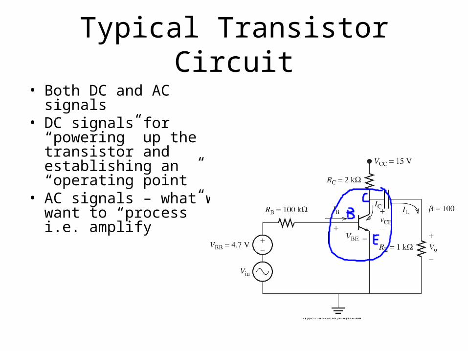
Typical Transistor Circuit
• Both DC and AC signals• DC signals for “powering”
up the transistor and establishing an “operating point”
• AC signals – what we want to “process” i.e. amplify
8
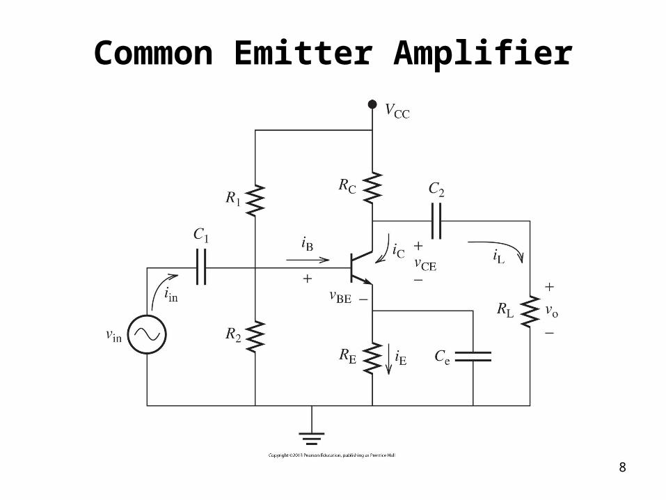
Common Emitter Amplifier

9
Common Emitter Amplifier
DC Equivalent Circuit

10
Common Emitter Amplifier
AC Equivalent Circuit

How Do We Handle Trans ??
• Determine “operating mode” and replace transistor with appropriate model (linear!)

12
Analysis Method

13
Analysis Method
14
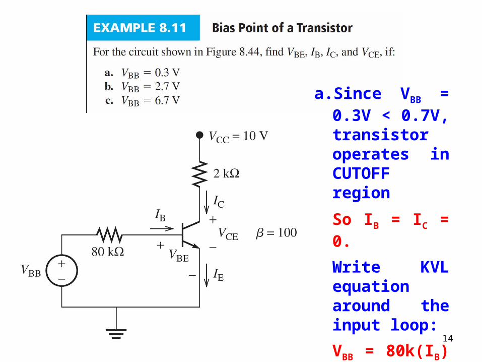
a. Since VBB = 0.3V < 0.7V, transistor operates in CUTOFF region
So IB = IC = 0.
Write KVL equation around the input loop:
VBB = 80k(IB) + VBE
VBE = 0.3 V
Write KVL equation around the output loop:
VCC = 2k(IC) + VCE
VCE = 10 V

15
b. Since VBB = 2.7V > 0.7V, transistor is ON and VBE = 0.7V
Write KVL equation around the input loop:
VBB = 80k(IB) + VBE
IB = (2.7 – 0.7)/80k = 25 A
Assuming ACTIVEmode, IC = IB
IC = 2.5 mA
Write KVL equation around the output loop:
VCE = VCC – 2k(IC) = 5V
> 0.2V, so transistor IS in active region

16
c. Since VBB = 6.7V > 0.7V, transistor is ON and VBE = 0.7V
Write KVL equation around the input loop:
VBB = 80k(IB) + VBE
IB = (6.7 – 0.7)/80k = 75 A
Assuming ACTIVEmode, IC = IB
IC = 7.5 mA
Write KVL equation around the output loop:
VCE = VCC – 2k(IC) = –5V
< 0.2V, so transistor is in SATURATION region
IC = (VCC – VCE) / 2k = 4.9 mA

TransistorsField-Effect Transistors
TransistorsField-Effect Transistors

TransistorsFET
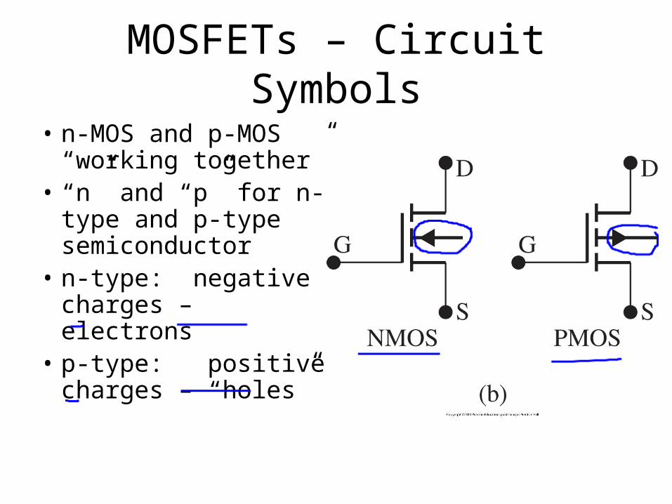
MOSFETs – Circuit Symbols
• n-MOS and p-MOS “working together”
• “n” and “p” for n-type and p-type semiconductor
• n-type: negative charges – electrons
• p-type: positive charges – “holes”

TransistorsFET
When VG is positive, electrons in the p-type substrate are attracted to the oxide–silicon interface, and form an n-type conduction channel. The electrical model is represented by resistors in series. The transistor is in its ON state.
NMOS

TransistorsFET
When VG = 0, the area underneath the oxide layer is still p-type, which forms a “back-to-back” diode with the n region, as shown in the electrical representation. The transistor is in its OFF state.
NMOS

TransistorsFET
PMOS

NMOS vs. PMOS - Operation

NMOS vs PMOS
INPUT NMOS
High “1” ON
Low “0” OFF
INPUT PMOS
High “1” OFF
Low “0” ON

NMOS Inverter• What happens
when Vin is “high” ? i.e. logic level “1”
• What happens when Vin is “low” ? i.e. logic level “0”
100011110100111010001110
INPUT OUTPUT
High “1”
Low “0”
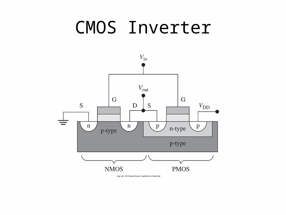
CMOS Inverter

CMOS Inverter
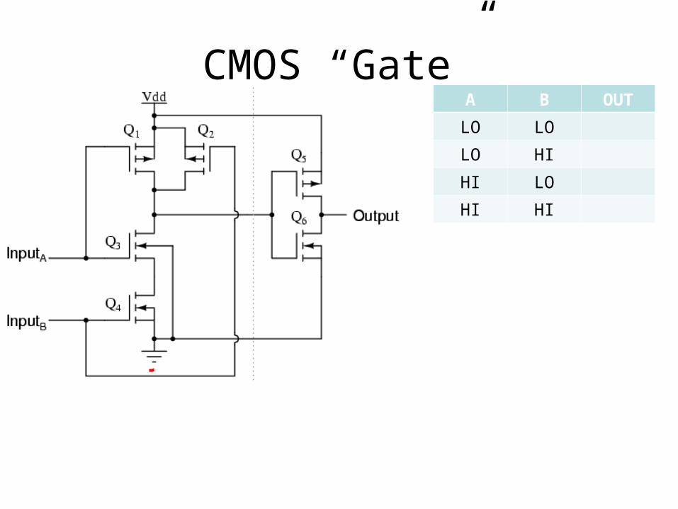
CMOS “Gate”A B OUT
LO LO
LO HI
HI LO
HI HI

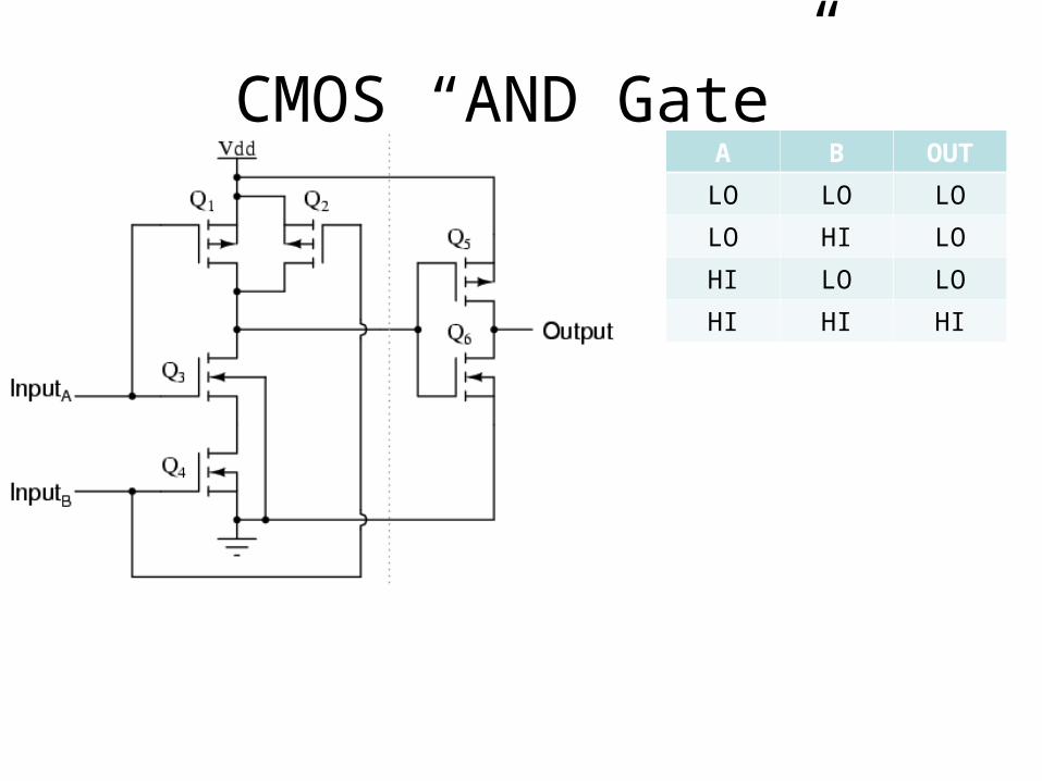
CMOS “AND Gate”A B OUT
LO LO
LO HI
HI LO
HI HI

CMOS “AND Gate”A B OUT
LO LO
LO HI
HI LO
HI HI
CMOS “AND Gate”A B OUT
LO LO LO
LO HI LO
HI LO LO
HI HI HI

CMOS “AND Gate”A B OUT
0 0 0
0 1 0
1 0 0
1 1 1
Related Documents