DEPARTMENT OF WEAPONS TRAINING= LUJRY AIR FORCE BASE . COLORADO» TRANSISTORS IN SEVICE TRAINING COU'.B.SE' 1 I .:_';*"xq" __:IIl ;_' ( ‘\ ' . * my / E 26 July 1961 I I 5'” ,___ Iii-n A ' A o“ - "@ \ cwwm 4 Av“! Q, /$1? 4149- - " ' §* #3 . ‘f "51 ff} THE JUNCTIGI\T TRANSISTOR °= ‘" M 0;‘MX Q, _— / \ FOR INSTRUCTIONAL PURPOSES ONLY “Q

Welcome message from author
This document is posted to help you gain knowledge. Please leave a comment to let me know what you think about it! Share it to your friends and learn new things together.
Transcript

DEPARTMENT OF WEAPONS TRAINING=
LUJRY AIR FORCE BASEA
. COLORADO»
TRANSISTORS
IN SEVICE TRAINING COU'.B.SE'
1 I
.:_';*"xq" __:IIl ;_'
( ‘\' . * my
/E
26 July 1961I I 5'” ,___ Iii-n A ' A
o“ - "@ \ cwwm 4 Av“! Q,/$1? 4149-
- " '§* #3. ‘f
"51 ff} THE JUNCTIGI\T TRANSISTOR
°= ‘" M 0;‘MX Q,
9“' $9
.0
_—
/
\
FOR INSTRUCTIONAL PURPOSES ONLY
“Q

CHAPTER AAuthor: A16 Robert Jo Widlsr
THE JUNCTIGN TRANSISTGR
Abstract — The operation of the junction transistor is explained in detailconsidering the junction barrier, minority carrier injection, space chargeneutralization and diffusion phendmenone Furthenmere, the physical andelectrical parameters affecting transistor perrormsnee are given considerableattention. The inherent temperature sensitirities of the transistor arepointed out, and the factors contributing to s general deterioration ofperformance at high frequencies are enalyzedo Modifications of the basictransistor that will greatly extend the maximum operating frequency aredescribed. Finally, transistors that exhibit thyretron-like characteristicsare discussed along with other single and multiple junction devices intendedfor special applications. '
i
NPN $1‘ IUGYUHI
IIMYYIK CONTILT
COLLECTOR Fm
EMWYIR Pm-P "
MIT» MS!
L.0’!if
I‘|__d!
4 GME \'-UNVAK1’
3 bl-A55 llA\_
/\\
3/\
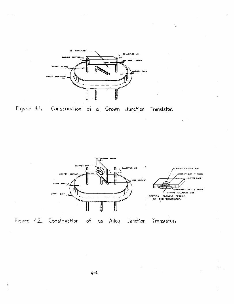
Figure 4.1. Consfruchon o¥'<.1. Grown Juncon Trans'|s+or.
EMIFTIK
‘RSI WAFER
DU? \n F11%“ ~muvvlk ¢-ON'rAr.'r (—;u_..____
/
¢='-\-I¢T°K "ll w-Tvn: uvnnw-en, nor
' numsrmun P nmmui\\ ms: ¢onrM.1- M-"PE “S:‘I‘-W‘ "*'- D 1/ ” /.~.=I_ ,.-.: -:_,='.- _»
, F\ltRY$1'A\.\5\'.D P Re-uou
M-_'_A‘ 5”‘ ' \ I QPQWPI?» <,o|.|-.Ic:rOK B01‘"2’\ secmou suowme DETMLS
&_,_
w I
4-1
' OF E ‘T " TO\‘ TH RAN-.al5 R
7»§;ur‘e 4.2. Conskrucon 0’? an Aoq Junc’r'\on' Trqnsusior.

INTRODUCTICN
In chapter l an elementary description of the junction transistorwas given» The NPN an PNP structure of the transistor wes shown, anithe paths of the current carriers were illustratedo Here the potentialbarriers existing st the junctions will be taken into consideration,and the mechanisms responsible for the transport of current carriersacross the base will be looked into more closelye Furthermore, thedesign factors affecting performance (current gain, linearity max-nnm ratings, temperature sensitivity, and frequency response; willbe discussedo Finally, special designs used to improve character-istics for particular applications will be coveredo This lettercategory will include the driftg tetrodeg field effectg hook, andunijunction trsnsistorss i "
THE JUNCTION TRANSISTR
Two possible configurations usd in the fabrication of junctiontransistors are illustrated in figures A01 ed £020 These will bediscussed briefly so that the nature of the device can be eppreciatedeHowever, s more detailed description of msnnfectnring teohniqnes willbe given in the next chapters ’
Figure A01 illustrates s grown junction transistors A NPNtransistor of this type is made by dipping e seed orystsl into modtengermanium which has been moderately doped with s N~type imurityoThe seed is withdrawn slowly from the melt; and the doped germsninmwcrystslised on the seed$ producing e N=type crystals After thecrystal hes grown for some times sufficient Petype impurity is eddedto the melt to overcome the N—type impurity; en e thin Pmtype layerhssing e high resistivity is growno Finsllyg en excess of Netypeimpurity is dumed into the melt, egein/reversing the imnrity typesso e low resistivity N-type portion is growno This procedure givesthe reqnired NPR structures Using this teshniqneg good quelitytransistors haying hese widths in the orderlof ©0991 inch csn be 1
m@d$o
An alloy junction trsnsistor is shown in figure A020 Tofsbricnte this type of transistors two dots of e Petype impuritynesing e low melting point ere placed on opposite sides of s thinNetype germenium.wefer which hes s high resistivityo this sssemblyis then heated, melting the dots which take some of the germaniuminto solutions When the assembly is coeledg the dissolvd germanium,which is now heavily doped with the Petype impurityg reorystslises»on_the wafer around the dotso This procedure yields two heavilydoped P-type regions separated by e thin layer of lightly doped Netypeymeterielo In practice, the penetration of the dots into the wafercan be controled to produce bsse widths of G@G0l~000O3 inche N
Q2
gs
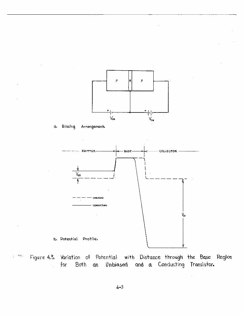
Figure 4.5.
+~|1
q. Blessing Arrangemeni-.
"'——-—-*-- EM \TT ER >l<
+- ,||||
V“ Vca
V»
*'—"iUN5\ASED
\ *7-
@ \iii‘ CON DUCTING
b. Poi-enHa\ P\~oH\e.
Varied‘
\
\on 0? Poi-en’r‘ '
1°
\<1\ w|’rh
or Bo-kh
Disi-ance H1
an Unbias
BASE > u I‘ C.0LLE(‘.TOR'“—%—~—~
_\
rf“"
\\
\ k\
\
i
rough ’rhe Base Re '10
ed and a Conduc’r'
$6
g n
mg Trans‘\s+or.
/
Bsrrier Formations As with s junction diode, when the PR jungtiong'of s trsnsistor ere formed, there is en initial diffusion of current “
csrriers across the junction, which produces e charge unbalance, \Thischerge unbslsnce gives rise to e barrier potential and its associatedberrier fieldiht is confined to s nerrow depletion regions This ‘bsrrier opposes further diffusion and estsblishes en equilibrium consditiono Therefore, in an unbiased transistor, barriers will be formedst the emitter and collector junctions producing the potential profileshown in figure hQ3b (dashed line)°
Transistor 0oerstion,_ When s reverse bias is applied to thecollector junction es shown in figure A@3e, the barrier height at thcollector junction is increesed by on smount eqpsl to the appliedvoltegeo The entire collector voltage is dropped across the depletionregion of the collector junction, so there is no electric field actingon the current carriers in the base end in the collectoro Therefore,no current will flow ecross the collector junction, except for s smallssturstion current csused by the diffusion of thermally generated r _
minority carriers to the junctions 4 '
If now e smell forward hiss is applied to the emitter junction,this barrier will be lowered, permitting the diffusion of holes into,the bsseo It should be emphasized that the holes ere not acceleratedinto the bsse by the forward bies, but instead the berrier is loweredpermitting the thermal diffusion of holes through s reduced barrier,fiéldo Furthermore, after the holes ere injected into the base, theyere not scted upon by an electric field but continue to diffuse untilthey reach the collector junction. When the holes arrive at thecollector junction, they enter the berrier field which sweeps themscross the junction into the collector (the drift forces of the electricfield ere considerably stronger than the diffusion forces)~ ‘
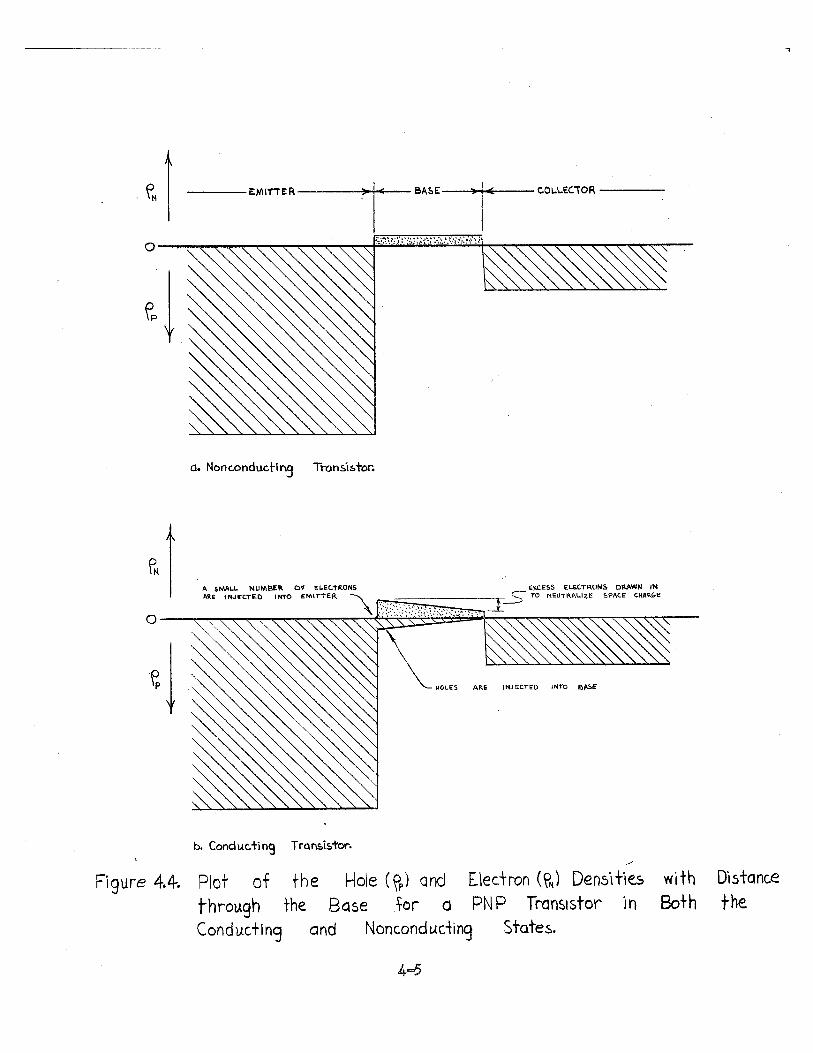
§psce Charge Neutralizstiono When the emitter junction is fore,nerd hissed, holes ere injected into the b@S@o These excess positivechsrges crests en electric field in the bese regions However, themobile electrons in the bsse ere scted upon by this field end areattracted to the positive chsrgeso Electrons ere then drawn in fromthe bsse terminal to neutralize the electric unbalance crested by theinjected hQ1@So This process, which hes slresdy been explsine inchspterl2, is celled specs charge neutrslizstiono The hole and electrondensities ere plotted in figure Ash es s function of distance in thevicinity of the base to illustrate this phenomenono .
x_ One result of spsce charge neutrslizetion is the elininetion ofthe repulsive forces noting on the injected holeso Therefore, theholes do not diffuse through the base by mutual repulsion, insteadthey ere trsnsported across the bees by thermal diffusion supported bythe higher concentration of holes nesr the injection source (emitterjunction)o
4c4
PM 1 ~—i—-EM|T‘TER 11; a/ass T (<:o\.\_ecToR---————--
§¢ F_k\\\“\\‘Q. Nonconducfin Tronslsfon
lA 5wu_|. uumazw. or :|.er:rR0ns amass use-rrxons DRAWN nu
ARE m.n:c1-E0 mm smrrvea \ 5 TO mau'mm_|zz 5PAcE CRANE-E
:3 ?.~"I:~".?1 i:?_:!“',r\§,;i.'.;~‘_~‘:;
O \ \ \\ \ \ "\ ‘ *
b. Conduc rag Trqnsis’r0r~..
ure 4.4. Plox“ of ‘me Hole (3.) and E\ec‘rr0n (9,) Dens‘\+'\es wi+h D‘\s’rQnc@
fhrough ’rhe Base ¥or <1 PNP Transnsfor 'm Bo’rh HEConducng and Nonconduding Sfafes.
A-==-5

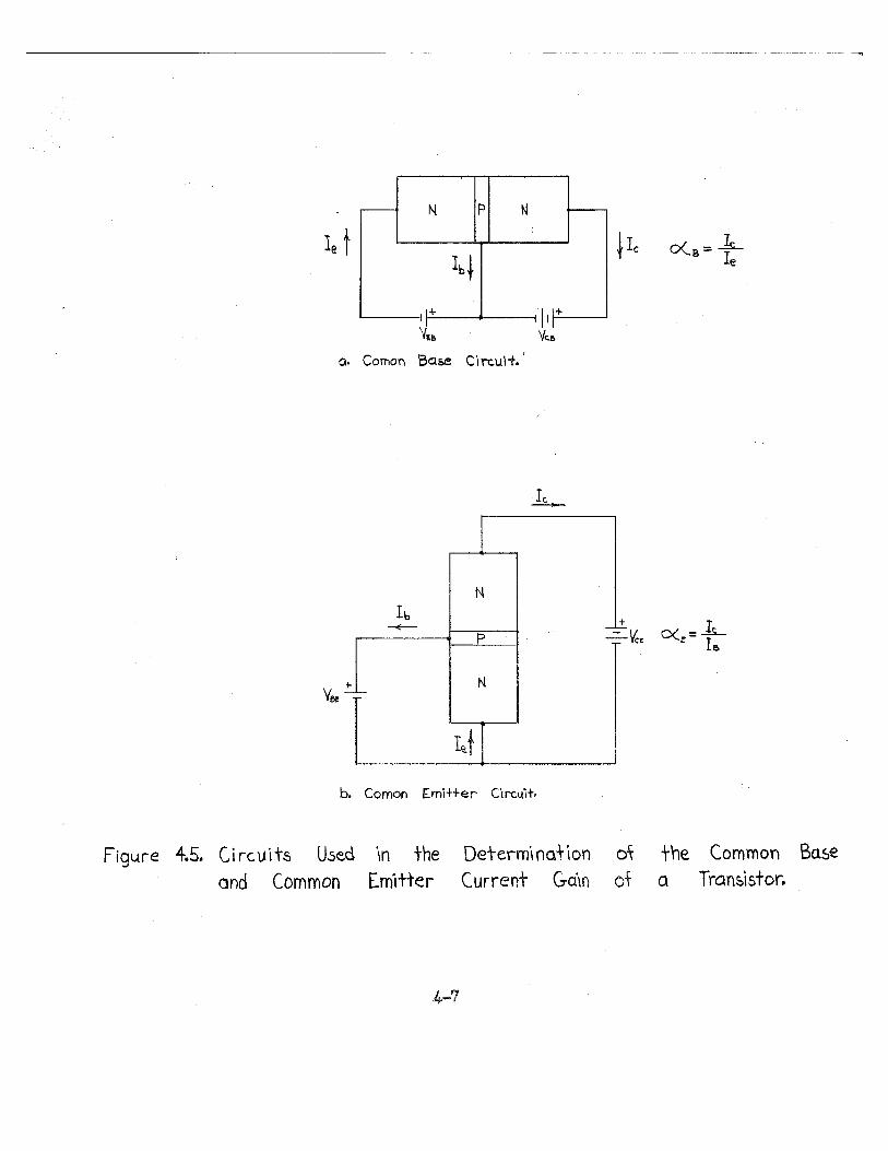
Current Gains Before going further into the operation of the 1
transistor, two parameters need to be defined: the common base currentgain (°35) and the common emitter current gain (=KE)» The commonbase deco current gain is defined as the ratio of the collector currentto the emitter current (figure h.5a)° It has been shown that thecollector current will be less than but very nearly equal to theemitter current for a junction transistor so _c<§ will approach unity.In practice, values of <><B~ ranging from 0¢900—0»995 are common.
The common emitter deco current gain is defined as the ratio ofthe collector current to the base current (figure h@5b)¢ Since thebase current is small in comparison to the collector current, ¢(; ;
will be considerably greater than ones Values of ¢<5 correspondingto those given for o<B range from 10-200. (Note: the comon emittercurrent gain is sometimes given as the beta Q current gain.)
.- \
TRANSISTUR PERFORMANCE
The current gain of a transistor can be determined by consideringthree terms: the injection efficiency, the transport efficiecy, anthe collector efficiencye The physical phenomena affecting these termssill be investigated for a PNP transistor, although analogous reasoningcan be applied to e NPN unit.’ V
Injection Efficiencye When the emitter junction is forward biased,holes from the emitter are injected into the base; and electrons fromthe base are injected into the emitters These hole and electron currentsconstitute the total emitter current» It is desirable to make theelectron current across the emitter junction as small as possible tbg¢auS@ it produces a base an an emitter current but it does not con-tribute to the collector currents The electron current, then, reducesb01311. <><5 $115» ‘°<Eo
The injection efficiency is defined as the ratio of the holecurrent across the emitter junction to the total emitter currontdHigh injection efficiencies (near unity) can be realized by sup:pressing the electron current across the emitter junctions 0n»method that can be used to accomplish this is to make the emitter ofa heavily doped; low resistivity material and make the base ofealightly doped, high resistivity material. Hence, when the emitterjunction is forward biased, a larger umber of holes will cross thejunction by virtue of the fact that there is a much higher concen-tration of holes on the emitter side than there is electrons on thecollector Sid$o
The injection efficiency is also affected by the base widthand the minority carrier lifetime in the emitters When the emitterjunction is forward biased, the hole concentration on the base sideof the emitter-base junction and the electron concentration on the'
h-6
~aM Id we °<“‘%°T
»|* i W\\/ea \/ca
0» Comon Base Circu‘:-f.'
IL
N
-<5 V-2 =;@_-1 —o;~\/Q <><E I5
Vs:+ N ‘
M \
b. Comon Emi++er~ C'=rcui+-
Figure 4.5. Cirouifs Used '\n ’rhe De‘rerm'mcrHon 0% We Common Base
and Common Em‘|’r’rer Currenf Gum 0’? c\ Trc\ns‘|s+or.
£,,==-7
emitter side of the smitter—base gunction will be determined by theresistivities of the emitter and ase materials respectively and bythe forward bias. However, the currents resulting from these injectedcarriers will be determind by the factors mentioned below,
The effect of base width on the hole current across the emitterjunction is illustrated in figure h.6¢ Since all the holes reachingthe collector junction will be swept into the collector by the reversebias, the hole concentration at this point will be near zero; and thevariation of hole concentration with distance through the base will beas shown in the figure. The diffusion current produced by these holeswill be proportional to the abruptness of this variation. It shouldbe evident frm the figure, then, that the hole current through the .
base will be inversely proportional to the base width.
Since there is no sink for electrons in the emitter as there was’for holes in the base (the collector junction), the point at which theelectron concentration in the emitter reaches a neglegible value will“be determined by the minority carrier lifetime in the emitter. iThatis, if the electrons injected into the emitter recombine rapidly, thefall off in electron concentration will be abrupt. This is illustratedin figure A970 Because the electron diffusion current will depend onhow fast this concentration falls off, it will be strongly affected bythe minority carrier lifetime. Actually, the diffusion current isinversely proportional to the diffusion length which has been definedas the average distance that a minority carrier will diffuse beforerecombination occurss ‘ j
To summarize, a high injection efficiency can be realized byproducing a transistor which has a narrow base having a high resistivityand a low resistivity emitter with a long minority carrier lifetime. Y
In practice, it is not too difficult to realize a hole current 1000times as great as the electron current, which gives an injectionefficiency of 0.999.
lggnsport Efficiency» The next term to be considered is thetransport efficiency, defined as the ratio of the hole current acrossthe collector junction to the hole current across the emitter junction.The transport efficiency will be a function of the number of holes19st in the base region by recombination. There are two significantsources of recombinations" volume recombination and surface recomrbination. '
The volume recombination, which is the loss of current carrierswithin the body of the base region, is best described for this purposeby the diffusion lengthe If most of the holes crossing the emitterjunction are to reach the base, the base width must be small in .
comarison to the diffusion length» Typical values of diffusionlength are from 0°05 to 0.005 inch. Hence, with a 0.001-09002 inch
h—8

---- zwrnzrz ~ W >1‘-6 f BASE
%
*1»
TORN
C
UN(.O
7Oi \\
K\,\\\\>>>\“~ *
Q. W\de. Bose.
-——— EN\\TTER———a-‘ BASE 8<—
b. Narrow Base.
Figure 4.6. Flor 0? rhe Hole Concen’rrc1’rion +hrough +he Base 01‘ Q PNP j
TF¢\$i§’r0F $0? <1 Given Forward Bias, +0 Show rhe EHcc+0% Balsa \/\/?d+h on Hole D'\¥%us'\on Current
OLETO
NTON
;;._\_ r; .
.. .\..\.\r‘
5' »,\'_:. .
PM __. 1 . _. \ _.
. ._.\- :1 ‘I51 ‘T_g:‘_~‘_=§:_§ 5 ‘_. --._~\-:.~_1:—_.~__~=~. .-O 1.-,-_<..._.~_~_.____.-_\_» .-_.‘ _.;.._‘._ \ ‘_~ , _-_; ‘._ 4,
Q. Long Leme. A
-——i~———————~ EN\lTTERi————-—-—>- BASE -<—\~"‘~‘;r. 4. \. 0.'.-~.\\\~;’‘~\ -\\‘_.\~'..‘\\ ~\ _\
:‘\'|?1;‘-a-‘ \: _.. - ,=.-\"""-u.~;_; r\ . ,..§.1-¢\_ 3_._.\\~‘\QZT ];==‘.=-z:-:1-2
O ,_-~“‘~ ;.‘I:::'l'31: 1
b. snow Li¥e1-ime. _
Figure 41 Plo’r 0‘: Eiedrron Concen+ra‘rion Kn We Ernier 0’? <1 PNP Trons'\s’ror
for <1 Given Forward Bias, +0 Show +he EHec'\' of M'\nor\’n3
. Carrier L'\¥e’r'\me on E\e.c’r,ron D'\¥¥us'\on Current
4-9

thick buss, volume recombination in the base region will be smalls Thenumber of carriers lost by volume recombination increases quite rapidlywith increasing base width nd with decreasing diffusion lengtho For”e diffusion length of O@O5 inch and a base width of 0,005 inch, approx-imately 0.02 percent of the carriers are lost by volume recombinationin traversing the base; and for s diffusion length of 00005 inch and »
e buss width of 00002 inch; about 8 percent of the carriers are lost.
The second source of recombination, surface recombination, takeslace when injected minority carriers diffuse to the surface of the
gees, become trapped, and eventually recombinee The surface recoms .
hinstion losses will doped on how much bese-surface area is in thediffusion path of the holes crossing the beset It seems likely, then»that this term is unimortunt in a grown junction_transistor (figure 4,1)which has very little base—surface sreeo In an alloy junction tren-sistor (figure AOQ) which hes e large base—surfsce ares, surfacerecombination is usually more imortsnt than volume recombination.
If the minority carriers diffusing to the surface of the baserecombine slowly, the minority carrier concentration at the surfacewill be relatively high, inhibiting further diffusionc The rate ofdiffusion to the surface and, therefore, the number of carriers lostby surface recombination, will then depend on the recombination rate.of the carriers trapped at the surface, or the surfgce recombination .
velocitgs The recombination rote is determined by the condition of e
crystal surface: rough, contaminated surfaces give high recombinationvelocities while clean, etched surfaces that are free of defects.give low recombination velocitieso ‘
, :
~>Qollector Efficiencyo ,The last term used in the determination ofcurrent gain is the collector efficiencyt The collector efficiency isdefined, for a PEP transistor, as the rutio of the hole current across~the collector junction to the total current across the junctiono Thetotal collector current can become greater than the hole current aloneif carrier multiplication occurs within the collector junction or ifte e
significant number of thermally generated electrons in the collectordiffuse to the collector junctions
Avalanche multiplication can take place within the collectorjunction if the reverse bias on this junction is made sufficientlyhighs At high reverse voltages, it is possible for the holes crossingthe junction to be accelerated enough to produce ionizstions when theycollide with atoms of the crystal lattice, producing additional currentcerriersg This can occur at reverse voltages below the breekdownvoltage of the junction (self sustaining multiplication) and will f
produce common base current gains (“=*3 ) greater than oneo More willbe said about avalanche multiplication in the discussion on reversebreakdown phenomenonc
h—l0

\50
G-A.N°<=\
~_¢
C.UR5ENT
8TTEIR
,-
commomEv\
8
Figure 4.8. \/cu~io\+'\on o§- Common Emier Curren’r Gain wrh
Collector Currer ¥0r Grown and A\\og Jundnon
>
>
‘
uUNC1
* ~; AL 73?my
~w~¢TIo~ ~/v ,$7_oR
I TRAN$|§"|"oR%\I
COLLECTOR CURRENT
_ Transidorg. '
4=-11

Uner normal circumstances, the flow of holes into the collectorof a conducting PNP transistor does not affect the diffusion ofthermally generated electrons to the collector junction, so the g
collector current is equal to the hole current across the collectorjunction plus the small reverse saturation current of the reversebiased junction» Therefore, the collector current is essentiallyequal to the hole current; and the collector efficiency is unity.However, if a high resistivity collector material is used (whichmeans that the hole concentration is relatively low and that thethermally generated electron concentration is relatively high),the flow of holes into the collector will produce a significantincrease in the hole concentration near the collector junction andwill give rise to an electric field near the junction» This electricfield will act on the thermally generated electrons in the collectorspeeding them toward the junction, thereby increasing the collectorcurrent, If the resistivity of the collector material is sufficientlyhigh, this effect will produce an ap reciable increase in collectorcurrent (over the hole current alone§ and increase the collectorefficiency above unity» ' t
Imroving current gain by increasing the resistivity of thecollector material is generally undesirable, Th8 rcasns for thisare given» First, it is possible to realize common base currentgains slightly greater than one by this method. Second, if thecollector current does become greater than the emitter current (c%l3greater than one), the direction of the base current reverses; andthe transistor becomes unstable. In this condition, the transistoris useful only in special applications which require a common basecurrent gain considerably greater than oneo And last, when a highresistivity collector is used, the current gain will increase rapidlywith temperature as the number of thermally generated electrons inthe collector increases. Hence, ‘*3s ‘will become greater than one;and the transistor will become unstable above a certain temperature»
High Current Operation» In the treatment of transistor operation,thus far, it has been assumed that the collector current was lowenough that the injected minority carriers did not appreciably alterthe majority carrier distribution in the b@$o At higher currentlevels the injected minority carriers will produce a significantincrease in the majority carrier concentration in the base near theemitter junction because of space charge neutralizationo Thisi‘causes the variation in current gain with collector current illustratedin figure Ae8°
The collector current in a PNP transistor is increased byincreasing the concentration of injected holes near the emitterjunctions This provides a sharper variation of hole density withdistance through the base and increases the diffusion current to the
4-12

100-
(9%)
2$
CURRENT
LnO
EMTTERCOMMON
wcn
\|01
v
I
i|
1
it
__7________ __ ______ 77 77%
I : l I° 5 :0 as 20 soCOLLECTOR VOLTAGE (volts)
W4 I
25
Figure 4.9. \/<1\"ic1’Hon 0‘: Common _Em':’n“er Curvenf Gain wh Coedor
\/o\+agc-:- ‘
4-13

collector junctions These injected carriers create an unbalancedcharge distribution which is neutralized by excess electrons drawnin at the base terminalso Hence, the density of free electrons in thebase will be higher near the emitter junction, as shown in figure 4.4.This does not reduce the electric field in the base to zeros A small;residual field must remain after space charge neutralization tosupport the uneven distribution of electrons since they will tend todiffuse and equalize their distributions For small collector currents,this field is also small so it has been neglected up to this point.However, as the collector current is increased, the distribution ofcurrent carriers in the base becomes more uneven necessitating anincrease in this supporting fiQ1do It can be seen from figure hotthat in order to support a higher concentration of electrons at theemitters the field must be positive toward the emitter and negativetoward the collectors This field is in the correct direction tospeed the holes across the bases
The increase in minority carrier velocity across the base increasesgthe current gain because the change of recombination is lessenede Thisis shown as the initial increase in current gain in figure #680 Thisinitial rise is more pronounced in an alloy junction transistor becausethe surface recombination term is quite important in the determinationof its current gains For good quality transistors, volume recombinationis small so there is only a slight increase with the grown junctiontransistor which has negligible surface recombinatione
After the initial increase, the current gain is found to decreessteadilye This is caused by a reduction in injection efficiencyresulting from the increased electron concentration in the bases
As the collector current is increased to high levels, the injected-hole concentration in the base becomes markedly greatero This requiresthat the electron density increase far above its normal value in orderto maintain space charge neutralityo This increased electron densitynear the emitter junction also increases the number of electrons injectedinto the emitters Because these injected electrons will contributeonly to the emitter and the base currents, not the collector current,the current gain of the transistor will fall Qffo _
The variation of gain with collector current is of great imortancein the application of transistors, particularly with power transistorswhich must supply large currentso The most practical method of main-taining current gain at high current levels is to dope the emitteras heavily as possible so that a large increase of the majority carrierdensity in the base can be tolerated before the injection efficiencydrops to an unacceptable valueo This is one reason why power tran-sistors are usually the alloy junction types The recrystalized semi-conductor material near the emitter dot is normally saturated with theimpurity contained in the dot so the emitter has a very low resistivity.
4-14

LO
(rm-3
gCURRENT
9CF‘
CDLLECTOHCUTOFFP
-P
O-Z1-T
\
v
I 7 7 "7' "NWT WW" Vwiw i
l IO 20 40 £10 810 Igo- {io
TEMPERATURE (“Q
Figure 4.50. Plo’r 01“ Co\\ec’vor" Cwvo Curfew versus Tempe"r"on“i1r€ ‘ror
<1 Germanium §r"<:=@'x:{ss*‘ror.
4-15

Yariation of Current Gain With Collector Voltages The resistivityof the collector material is usually considerably lower than the resis-tivity of the base materials Therefore, the depletion region of thecollector junction must extend primarily into the base in order to _
expose an equal number of immobile impurity atoms on either side of tejunctions Furthermore, when collector voltage is applied, the depletionregion will become wider and will penetrate further into the base,narrowing the effective base Widtho This will increase both the emitterand transport efficiencies and will therefore increase the current gainof the transistoro Base width modulation by the collector voltage isillustrated in figure he3b, and the effect of collector voltage oncurrent gain is plotted in figure h°9°
TEMPERATURE DEPENDENCE
Since the properties of semiconductor materials vary widely with.temerature, the performance of semiconuctor devices, including thetransistor, can be expected to be temperature sensitivee The temper-ature dependence of semiconductor materials has already been discussedat some length in Chapter 20 It has been shown that the thermalgeneration of hole—electron pairs increases rapidly with temeratureand will eventually cause a dopd semiconuctor to loose its charac-teristic properties as the number of thermally generated carriersbecomes appreciable comared to the number of majority carriers inthe materials Furthermore, it was pointed out that the mobility ofthe carriers decreases with increasing temperature because of theincreased thermal vibrations of the crystal lattices Finally, it wasexplained that the thermal energy of the current carriers increaseswith temperature which strongly affects diffusion phenomenae It turnsout that the diffusion current for a given density gradient increaseswith temperature as does the diffusion lengths
Collector Cutoff Currents Since the collector junction is reversebiased, the thermally generated minority carriers present in the baseand the collector will diffuse to the collector junction and will beswept across the junctions These carriers will then produce a collectorcurrent, even though the emitter junction is not forward biased. Thisuncontrolled collector current is called the collector cutoff current.
Since the number of thermally generated minority carriers willincrease rapidly with temperature, so will the collector cutoffcurrents This is illustrated in figure A010 which is a plot ofcollector cutoff current as a function of temeraturee At normaloperating temperatures, this current is quite small, if not negli-gible; but at higher temeratures, it will exceed the normal operatingcurrent of the devices When this happens, the emitter junction will '
loose its control of the collector current, and the transistor c
becomes useless as an amplifiers
4~l6

_—""" ,/_
(°<E
.-
GAN\l\TTE-RCURRENT
-...
COMMONE
Figure 4.H. Variaon of Common Em'|+’rer Curren’r Gcian w‘|’rh Temperahxre
l50-‘- ~
\O0-‘-
50
0-, 1 I 1 x a ( 1 1
-- 0-
—1o0-§-
-I50 -
»
4’-
//
| /(""---____L\_/1} \\>_Vg__/ /’ \\_i \
______________.____;
\
\
‘4'“T
* TEMPERATURE (‘=0 '
-20 O 2° 40 60 80 I 00
LEGEND:
————-i enown JUNCTION -rmmsxsroa wn-HH|eH CDLLQCTOR R!-:.Sl$T1V|TY. '
——-———-GROWN uuwcnou ‘rRANs\$-TOR wn-HMODERATE ¢o\_\.:c1-on REs|5T\v|TY» ‘
——— — —.— ALLOY JUNCTION TRANSLSTOR.
{or Di‘?\°eren‘r Trans'us’ror5.
4-17
////‘
Reduction of Emitter Junction Resistance» For a given forwardbias voltage, only a certain number of majority carriers have enoughthermal energy to diffuse across the lowered barrier of the emitterjunctions However, the average energy of these carriers will increasewith temperature so a greater number can cross the junction, Thisgives an increase in current with no increase in voltage, or arduction in the emitter junction resistances This takes place overthe entire temperature range of the transistor, and it therefore hasa pronounced effect on its biasingo
Effect of Temperature on Current Gains Figure 4°11 shows thevariation of current gain with temerature for several types of tran-sistorso The causes of these changes will be discussed in relation tothe emitter, transport, an collector efficiencieso
The emitter efficiency is not greatly affected by teperatureoTemperature affects the injection efficiency of NPN and PNP transistorsdifferently because the mobility of holes is reduced more than the‘mobility of electrons at higher temperatures, The net effect is thatat elevated temeratures there is a slight increase in the injectionefficiency of NPN transistors while that of PNP transistors remainsessentially constant;
In a grown junction transistor, the transport efficiency generallyincreases with temperatures The higher thermal energy of the currentcarriers speeds diffusion through the base, which lessens the chanceof recombination» However, the transport efficiency in an alloyjunction.transistor might well deteriorate at higher temperaturesbecause of increased surface recombination. The variations in thecurrent gain of an alloy junction transistor shown in figure A.ll'are,probably caused by changes in the transport efficiency“ At first, thecurrent gain increases with temerature because of the more rapiddiffusion through the bass; but at higher temeratures, surface recomrbination predominates, reducing the current gains
If the collector is made of highly doped ssmiconuctor material,the collector efficiency will be very close to unity over the entiretemerature range of the transistors This is true for an alloyjunction transistors However, in a grown junction unit, the resistivityof the collector is frequently not mch higher than that of the base.In this case, as was mentioned before, the holes drawn into thecollector (of a PNP transistor) can produce a significant increase inthe hole concentration near the collector junctions This will giverise to an electric field which will act on the thermally generatedelectrons in the collector speeding them toward the junctions Theseelectrons will be swept across the collector junction into the baseand will contribute to the collector current, but not to the emittercurrent, The number of thermally generated electrons in the collector
4~l8

[ ‘I
will increese with tempereture end so will the collector currentoThereforeg the collector efficiency, end elso the current gein, willincreese with temereturee
it e sufficiently high temeretureg the collector current canbecome greeter then the emitter currentg whereupon the direction ofthe bsse current will reverseo This is the ceuse for the instabilityof the current gain shown in figure hell (solid line)@
In general, the current gein of e grown junction transistor willincrease with temperature since both the transport and the collector .
efficiencies increesee Furthermore, if the collector resistivity iscompereble to that of the beseg the current gein can become unstablest elevsted tempereturese The current gein of en elloy junctiontransistors howeverg can very in lmost any fsshion depending on therelative importance of the surface end volume recombination termsoThe curve given in figure hell is only one possible exemplee
Conclusionse Practically all the temereture effects mentionedsot in such e way es to increese collector current st higher temper-etureso As the collector current increases so does the power dissi-pstion st the collector junctiono This produces further heating endcould lesd to e cumulative condition known es thermal runeweyg whichwould ultimately destroy the unite Therefore9 transistor circuitsrequire some method of hiss stebilisstion on conensstion tomsintsin e reesonehly constent collector current over the operatingtemereture rsngee
GQLLECTGR BREAKDOWN VOLTAGE
‘ J _
The reverse hissed collector junction of e transistor is subjectto svelsnche or zener breekdown es nee the cese with the junctioniiodee A third type of br@@kQ@wm known es collector punch throughis else possiblee On the other henna the emitter junction is normellyforward hissed so its reverse hreekdown voltage is of little concernc
The bsse of e trensistor is e thin lsyer of high resistivity materielwhile the collector resistivity is nsuelly very much lcsere Thereforegthe depletion region of the collector junction will extend primarilyinto the beseg end it will become wider es collector roltege isincreessde it high collector voltegesg it is possible for thedepletion region to penetrete through the bees to the emitter junction,thereby providing s direct conducting path between the emitter end thecollectors This is known es Qellectol Punch thronghp is with theother breakdown mechenismsg collector punch through will not injurethe transistor unless the power dissipation becomes greet enough tocease thermal damage,
4r19

The breakdown mechanism in alloy junction transistors is almostfalways collector punch througho However, in grown junction units thecollector resistivity may not be much greater than the base resistivityIn this case, the depletion region will penetrate into both thecollector and the base regions; and the device will usually undergoavalanche breakdown before punch through occurso
Zener breakdown is rarely found in a transistor. The highresistivity of the base material makes for a wide depletion regionso that intense fields are not built up across the junction. Zenerbreakdown only occurs in PN junctions where both materials are heavilydopedo
HIGH FREQUENCY GPERATIGN
The transistor has some rather severe high frequency limitations.Alloy junction transistors are restricted to operation below a fewhundred kilocycles, and grown junction units will not operate abovea few'megacycles° (However, special constructions can be used whichwill function at frequencies higher than 500 megacyclese) The rea-sons for these limitations and some of the techniques used to improve?high frequency performance will be investigated hereo
Transit Times Since the transport of minority carriers throughthe base takes place by rather slow diffusion processes, it will takean appreciable length of time for a signal applied to the emitterjunction to reach the collector junction. When a signal is appliedto the input of a transistor, it will modulate the number of minoritycarriers injected into the base and alter the minority carrier densityin the base above and below the no-signal value. If the input fre—quency is made sufficiently high, the amplitude (or phase) of thissignal will vary with distance through the base because of the finitetransit times Figure A012, which is a plot of minority carrier densitywith distance through the base, illustrates this points
In the time it takes for the signal to move through the base,the random diffusion forces will act to equalize these density vari-ations es shown in the figureo Hence, the amlitude of the signalreaching the collector is considerably lower than that at the emitterjunctions This results in a low current gain at higher frequencies.
Diffusion Capacitance. If a voltage step is applied to the inputof a transistor, the collector current will not rise immediately be— ,
cause of the finite transit time across the beset Furthermore, thecollector current step will not have a sharp leading edge because ofthe diffusion that takes place during the transport processe Theseeffects are shown in figure #013» Attention will now be focussed onthe input circuit to show another phenomenon associated with transittimé o
A—2O

OFMNORTYCARRERS
NBAsE_
EMTTERJUNCTO
////
Eou.oTORJvN<.
ENSTYD
N
Z‘.-_/ \Z
N0 JIGNAL CURRENT
|
I
\§+|<;H rnzau ENCY _surER\MPOsED
§ \
TONLE
oasrmca THROUGH BAsz-—->-
Figure 4.\Z. Hilus’rra’r'|ng ’rhe Rec§uc3r'\on in A-C Currerfr C-ain 0+ High Frequenuesby D'n°¥us'|on Which Equcdizes - Densg Variuons, a Consequenae
0¥ fhe F'm3+e Trans'a‘r Time across ’rhe Base.
RRERSCAORTY
.-
NSTYorMNNems:
EMWTER
/
/
LQQLQR
DE
\\ \\\ TRANS cur STATE\ 1
_ .
mn-mx. -STAT:-Z-I’/_
JUNCTQN
//i
/ /
JUNc‘FON
\ <F|um_ STATE
Q \ \ \
CO
- EMITYSR VOLTAGE
EASE CU RREN1"
ZMITTE R CU RRENT
Figure 4.\5. E¥¥ec’r 0‘? <1 Sudden \nc\"ec\se 'm ~\npu’r Vo\’rage on I\/\'mor'n‘y
msTANc£‘ THROUGH BASE--—->-COLLELTOR CU RRENT
Carrier Dis’rr'|bu+ion in Base. Em'|++er, Buse,<1nd Coedror
Curran"? Waveshapes a\so Given.
.4.-21

- - 4
hen the voltage step is applied to the emitter junction, theminority carrier concentration in the base will increase, or the basewill become charged. To charge the base region, an excess of minoritycarriers must be injected into the base over the emitter junction.Moreover, an equal number of majority carriers must be drawn in at thebase terminal to preserve space charge neutrality, These excess chargeswill not contribute to the collector current but will be stored in thebase until the bias on the emitter junction is again decreased. Hence,the emitter-base terminals of the transistor will appear as if theywere shunted by a capacitance, This capacitive effect, since it isassociated with the diffusion of minority carriers through the base,is referred to as diffusion capacitance,
The voltage step applied to the input of the transistor willproduce a transient current in the emitter and the base leads whichcharges the diffusion capacitance, In the transient state, theemitter current will be greater than the final emitter current becausethe diffusion gradient near the emitter junction (which determinesthe emitter current for a given forward bias) is greater than thegradient produced by the final current, This is shown in figure h.l3.The initial base current will also be considerably greater than itsfinal value because majority carriers must flow in at the base terminalto preserve space charge neutrality.
It can also be shown, in a similar manner, that a reverse tran-sient current will flow in the base and emitter to discharge the basewhen the emitter junction bias is decreased,
The diffusion capacitance will lower the input impedance of thetransistor at high frequencies. The signal source driving the tran-sistor must produce a current that alternately charges and dischargesthe base rather than producing a collector current» This representsa;loss of input signal and lowers the effective amplification of thethe device,
Ease Spreading Resistanceo The base spreading resistance is theresistance of the material between the base contact ad the activearea of the emitter junction, This resistance appears electrically .in series with the base terminal,
Since the base is made of high resistivity material and isnormally very thin, the base resistance can be quite large (severalhundred ohms)» Hence, a signal applied between the emitter and thebase terminals will be attenuated by the base resistance before itreaches the emitter junctions Furthermore, since the emitter junctionimpedance decreases at high frequencies because of the diffusioncapacitance, the signal reaching it will be even smaller at highfrequencies,
h—22

C-b'c
Bass I MNvW\ bl /\Nv\/MN CDLLELTOR
rbbl ¢ rb'<;
rh'e V53 —[' Cb'e \L 9mVb':
’ I
mmenQ- General Equ\va|en+ C|r~cuH-.
/
4r0uu¥
-———4/WWv\ I 'WWW\550:1. zmn _
\K£\- I \o.ooq.p§- 40 ma] v
b. Equ'nva\en+ C'\rc,ui+ 0*? c\ Low Frequency Alloy Juncon T\"0.n.s|.s'\'o\'*.
l-?iuu\'
_ WV50.0.. 5 MIL
1K-<1 Y "3D|uy.1§- (>0 ma! v
c.Equ1v<1len+ Circu‘\+ 0* Q High ‘Frequency m~m- Tmhslsfon
Figure 414. Equivalem‘ Cirr.u'\‘r Usel ‘m Eva\uu‘r'mg High Frequency Peormance
0*} a Transidror. 5pecH-ic, Examp\es ‘are \ncluded-
4-=23

iQollector Junction Cepecitsnceo The collector depletion region
forms en insulator between the conducting base and collector regions,so the reverse biased collector junction will behave cepecitivelyoThis collector junction cepscitence is considerably less than thediffusion cepecitence; but it shunts the high impedance collectorjunction, while the diffusion cepecitence shunts the low imedenceemitter junctiono Hence, st high frequencies, the collector capac-itance will frequently cause e greater loss of overall gain byshunting the output signal then will the diffusion capacitance bysunting the input signelo This cepecitence elso provides a feed-beck path between the collector end the bese so it can producedegeneration or instability at higher frequencies when the commonemitter configuration is usedo
in EhuivelentoCircuit@ The effect of the base resistance,the diffusion cepscitenceg end the collector cepecitsnce on thehigh frequency performance of e trsnsistor can be evelusted withthe aid of the equivalent circuit shown in figure_holLe¢ Theelements of this equivelent circuit cen be identified es: baseresistance ( flu ), emitter junction resistance ( Fw- ), diffusioncepecitsnce ( Cue ), collector junction resistance ( Tm ), col-lector cepecitence ( Cu. ), end the equivalent~circuit currentgenerator ( Qmwe )3 the terminal b’ is the internal base A
terminal (neer the active portion of the emitter junction), QMis the trensfer conductance (e quantity relating the emitter junctionvoltage 'Vk@ to the collector current)» end Vhe is the voltage onthe internsl bese terminal (emitter 5um1>i<m)Q c
This equivalent circuit does not take into consideration thedelay end reduction in current gain ceused by transit time ecrossthe bese so this circuit is not valid where this is the limitingfector of high frequency performenceo For most trensistors, though,this circuit is dequete over the useful frequency range of thedeviceo
Figure loll shows thet the portion of the input voltage appearingat the emitter junction (internel base terminel) will depend on thebees resistance, the emitter resistenceg the diffusion cepecitence,and the signel frequencyo The bese resistance is generally less thanthe emitter resistance so st low frequencies precticelly ell of theapplied voltage will eppesr st the internal bese and will be effectivein producing en outputs At high frequencies the reectence of thediffusion cepecitence will drop, resulting in en edditionel ettenruetion of the input signals It is therefore desirable to minimizethe bese resistance and the diffusion cepecitenceo
Some of the output signal appearing on the collector is fedbeck to the bese through the collector cepecitsnceo Since the col-lector voltege is out of phese with the bese voltsge (for e resistive
AFZA
load) this constitutes negative feedback and reduces the useful gainof the transistors If the transistor is working into an inductiveload, this feedback can become positive, possibly introducing instability.
The equivalent circuits of a low frequency alloy junction tran-sister and a igh frequency drift transistor are given in figure 4°14.The msximum.useful frequency of the former is in the order of 500 kcwhile that of the latter is about lO0mce The drift transistor has alower base resistance, diffusion capacitance, ad collector capacitancewhich permits operation at higher frequenciese
Imroving High Frequency Performances Some of the physicalparameters of an alloy or grown junction transistor can be alteredto raise the upper frequency limite These are reducing the basewidth, using a low resistivity base material, and reducing thecross-sectional area of the deviceo 0f course, this is not aninclusive list; but it represents some of the readily availiablemeanse
A reduction in base width will decrease transit time anddiffusion capacitance as well as increase the transport and injectionefficienciese The reason for the decrease in transit time should beobvious, and the decrease in diffusion capacitance results because anarrower base will store less charge. The increase in transport andinjection efficiencies have been explained previouslye A thin basedoes produce one undesirable result: the base spreading resistanceis increased because of the narrower current path between the activearea of the emitter junction an the base contacts Nonetheless, thisis more than compensated for, particularly at high frequencies, bythe reduction in transit time and diffusion capacitencee
Reducing base width is a very effective method of improvingtransistor performance; howevera with alloy and grown junction tran-sistors» base widths less than 00601 inch ere difficult to producewhich limits the usefulness of the methods
The use of a low resistivity base material will reduce boththe base resistance and the injection efficiencyo But if a transistoralready has a high injection efficiencyg a lower resistivity basecan give a significant imrovement in high frequency performance ate small sacrifice in low frequency gains This technique is partic-ularly useful in the design of video amplifiers where e flat frequencycharacteristic is more important than high gains
.Since the collector capacitance is directly proportional to thecollector junction area, this area should be as small as possible foroptimm high frequency performances A smaller crossesectional area ~
can also reduce the base resistance (depending on the geometry of thetransistor) by reducing the average distance between the base terminaland the active portion of the emitter junctiono This is particularly
A-25
true for grown junction transistorso On the other hand, a reductionin the cross—sectional area will also reduce the current capacity andmaximnm.power dissipation of the devices Furthermore, if the tran-sistor is made too small it will be fragile and difficult to manu-f@,CtuI°$o
SPECIAL TRANSISTQ5 -
Thus far the discussion on transistors has been relativelygenerals The phenomena described applies to the majority of tran-sistors, even though only the grown and the alloy junction transistorswere mentioneda In this section, special designs which have beenemployed to improve the performance of the basic transistor will beooveredv Furthermore, other PN junction.devices - which operatequite differently from the basic transistor will be explainede
The Tetrode Transistors The tetrode transistor differs from anordinary grown junction transistor in that two separate base contactsare needs These contacts are located on opposite sides of the baseas shown in figure A015. In operation, the emtter junction is for-ward biased by one of these base terminals ( h ) and reverse biasedby the other ( B2). Therefore, minority carriers will be injectedinto the base near the forward terminal onlyo This reduces thearerage distance from the active area of the emitter junction tothe B. terminal and the base spreading resistance when B, isused as the input terminals
i cross—base current will flow between the two base terminals.¢since there is a potential difference between them (for a NPN tran-sistor, 8| is about 005 volts and B1 about -l°5 volts withrespect to the emitter)“ However, the cross-base current willbe small because the base is made of high resistivity materials
The electric field set up by the cross—base bias will drawthe minority carriers, diffusing across the base, toward the B|terminals Thuss a number of these carriers, depending on the bias,will reach the base terminal and not the collector junctions Thiswill decrease the low freqnency current gain; but it is not aserious limitation since, at high frequencies, the reduction incurrent gsin is more than compensated for by the reduction in basespreading resistances This is proven in figure L016 which givesplots of the low frequency current gain, base spreading resistance,and 150 megacycle power gain as a function of cross-base ourrento
Another advantage of the tetrode transistor is that the B2terminal can be used to electrically control the gain of the device»This provides a convenient method of pplying automatic gain controlto a r—f amplifiers Furthermore, since the cross base bias willaffect the low and high frequency gains differently, it can be used
4-26

EMITTER
THIS PORHON OF‘ EM\T1lR JUNCTION FORWARD -:_:_:_:‘:—:_:_:_—”_‘——_~ 1-ms roux-non an mu-rev. Juucrnon RE\’EP6E amssnems!» av ?o.s|1-uvt 5| vm.1-M: -_-_._ _ _ _ _ ___'B"'_Z'-'__ sY NEGATIVE B; var-"mat A
+ "--- + + + @-__- -+B j * ~ B1
IN»-lE¢‘rI0v| TAKES PLME DNI-Y NEIQK 5| - - -- _.. _
_ COLLECTOR ’
Figure 4.15. Pq’rh 0% Minorg Camera ’rhrough ’rhe Base 0‘: O. Te‘rrode.
Trans'\s+or- Showing Reducion in Base- Spreading Resis‘\‘6lnc€-
L001! *
"' D415"
CURRENTcancu)
9D5‘.8
' ‘ t I I I° - 0'5 L0 1.: 20 2.5|4o<>..
I200-
s)TGNCEOh» §9Q
\.
BASERES58
O
400-
? 1 1~ r ;0 0.5 1.0 1.5 2-Q 1,5
l4-
I21-,_ \_, \
.0 |o-\-/
8" §.=\som=.56_
POWERGAN
Av~$>
0- 1 ( 1 1 ( : 1 2OS , LO [.5 . 1.9 7,5‘muss sass cumzaur (ma\
I-“sgure 4.\6. E¥~¥eq:+ 0% Cross Base Bias on ’rhe Charac’reris+ics 0% 0
“ Te+ro.de Tran.sLs+en
4-27

k I
to produce e reasonably flet frequency response in video emlifiersby reducing the low frequency gain to equal the high frequency gaino
The Drift Transistors It was stressed previously that thetrensport.of minority carriers across the base is accomplished bythe relatively slow process of diffusion with little or no aid fromen electric fi$1do In the drift transistor, the transport is greatlyeccelereted by establishing e built in electric field across the basein such e direction as to speed the carriers from.emitter to col-lectoro The electric field is crested during fabrication by dopingthe base materiel rather heavily near the emitter junction andtapering off the imurity concentration with distance toward thecollector junctions The majority carriers will tend to equslizetheir distribution because of thermal diffusion, but the impurityetoms ere fixed in the crystal letticeo Thereforeg there will bean initial diffusion of majority carriers toward the collectorjunctiono This will continue until the chsrge unbalance sets upen electric field which opposes further diffusiono An equilibriumis reeched with en excess of impurity ions near the emitter junctionand en excess of majority carriers neer the collector junctions Thisis illustrated in figure n—l7Q
The electric field crested in the base» opposing the diffusionof mejority carriers from emitter to collectors will he in the correctdirection to accelerate the minority carriers through the bees sincethey have en opposite chergeo
Goneidering, es an example, s NPN drift transistor, the scceptorconcentration in the P-type bese will he high neer the emitterjunction but low neer the collector junctiono The higher concen-tration of holes near the emitter will ceuse diffusion toward thecollectoro When equilibrium.is reschedg there will he en excess ofholes neer the collector end en excess of negative acceptor ionsnear the emittero Henceg en electric field will he establishedin the beseg positive toward the collector end negative toward theemittero When electrons ere injected into the beseg they will beeccelereted to the collector junction by this fi@1do
In eddition to reducing the trensit timeg the drift fieldmeterielly reduces diffusion cspecitenceo Since the minoritycerriers move foster through the bases e lesser number is requiredto produce e given collector currents Thereforeg less oherge willbe.stored in the b&5©o This is shown in figure LQl8o
Another advantage of the drift trensistor is thet the beesresistance is reduced by the high imurity concentretion neer theemitter junction which gives e low resistivity path for the besecurrento Although this might seem to reduce the injection effi-ciency9 it must be remembered that the minority carriers injected
#r28

I
wwu an-rv nous
DEN5TY
ii_'‘*3/ /
\_ X \Muoarrv unv.\:w.s—/1‘ \ _
. \ I
' \
V \
mm,-{g mu. 11>R
NSTANCE ‘THROUGH BASE
.-
- '~ _ u:\.\.eu'oR Juucon ~
.. \ .
.
FnoNrzsTY
>,- , I
" oacrr nzw—*. »
Y
. EM\T’TER JUNCTION HARDER
ELECTRC
L__ .
EMITTER ¢.ou.:r:ro:.<
< DISTANCE THROUGH BASE
Figure 4.lZ |\lus’rrang Form<1+'\on“0§" Q Bu'\\’r ‘an Ev\ec’rr'\c,.'Fie\d ‘m ’rhe Bose
of <1 Dr~iH* T'rc1nsis+or, ”Hav'mg ‘an Uneveri \mpur'\’ry Dis’rribu’r'\0n,
by 1‘he lniHa\ ,DH'~¥usion- “oi Majorifg Carers.
CARRERDEN$\T‘(
WITHOUT DRIFT HELD
' I
-[wntu DRIFT HELD |
—’— '-' ' ' * "'-_ \
MNORTY
;M|-r1-:5 ' ' t.OL|.l:C1'0R
D\5TAN(.F. THROUGH BASE .
Figure 4.\8 Comparison 03?‘ +he Minorvrg Carrier Concen’rra+‘ions in Hie Base
’ 0% <1 Trc1ns'\s’ror Requ'\red ’ro Produce Q Given CO\\€¢’fOF
Currenf vs/'\’rh and w'\+hou'\' +he Dr~'|‘r’r Field.
1 ma
‘F
into the base are acted upon by the drift field and are thereforemore effective in producing an emitter current than are the minoritycarriers injected into the emitter which must diffuse away from thejunctiono Therefore, even if an equal number of carriers cross thejunction in either direction, the injection efficiency can still behigho
The graded base resistivity of the drift transistor also assistsin lowering the collector capacitance since the high resistivitymaterial near the collector junction makes for a wide depletion region.
The merit of the drift transistor can be seen by comparing theequivalent circuits given in figure h.1h,
At high current levels where the concentration of injectedcarriers becomes greater than the majority carrier concentration,the performance of the drift transistor will deteriorate; and itwill operate as a diffusion transistor, This happens because ofthe distortion of the drift field by the injected carriers. It ison indirect result of space charge neutralization»
The graded base resistivity of the drift transistor is not asdifficult to produce as might be thought, This type of resistivityprofile is the natural outcome of man fabrication processes as willbe seen in the next chapter.
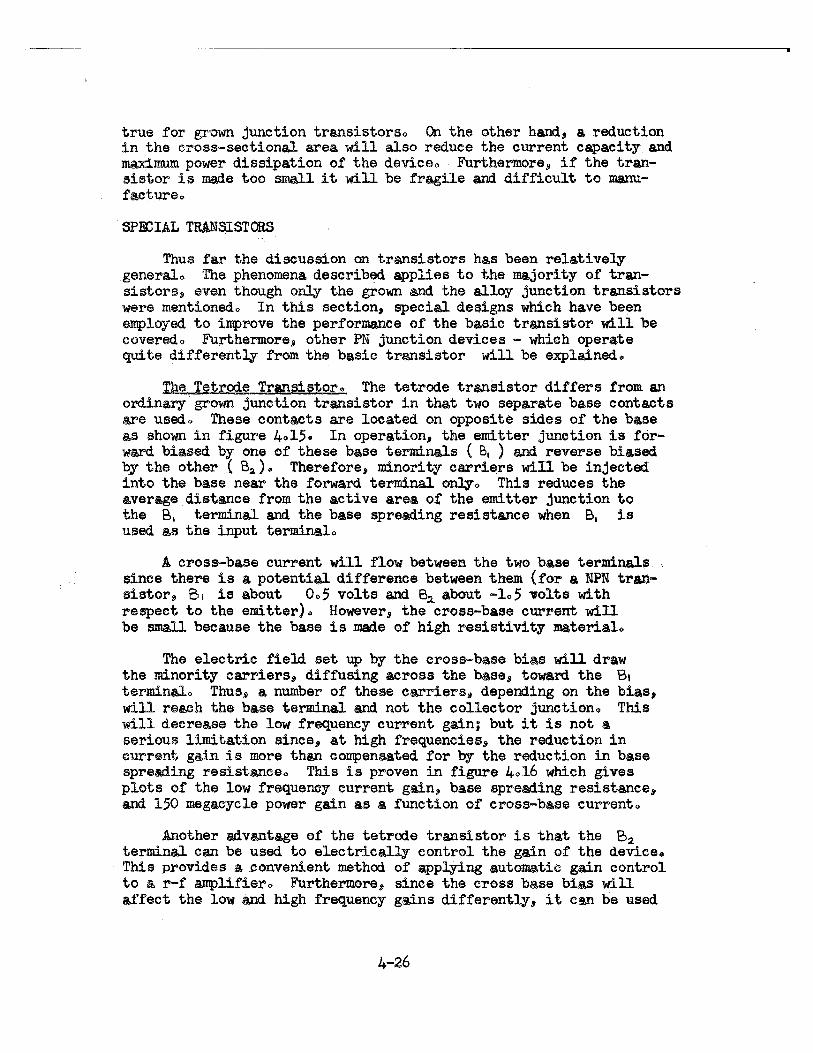
The Intrinsic Transistor. In the intrinsic transistor, alayer of undoped (intrinsic) semiconuctor is sandwiched between thecollector and the base. This gives a PNlP (or NPIN) structure asshown in figure h.l9= Since this layer contains no current carriers,the collector depletion region will extend through the intrinsicmateriel from the collector to the bases This produces a widedepletion layer, greatly reducing the collector capacitancee
The intrinsic layer can be made quite thick, yet it will notnppreciably increase the transit time: a strong electric field,produced by the collector voltage, exists in this region; this fieldspeeds the carriers through the intrinsic layer much more rapidlythan the diffusion forces take them through the base.
To appreciate the advantage of the intrinsic transistor, itmust be remembered that the collector junction capacitance providesa feedback path from collector to basee This greatly reduces thegain of a transistor operating as a wide band video amplifier andrequires that neutralization be provided for high frequency tunedamplifiers (common emitter), In the case of a video amplifier verylittle can be done to compensate for this feedback; and neutral-ization of tuned amlifiers cannot always be accomlished conven-iently, nor is it entirely effective because of base spreading
h-30
P"TY.PE F-MITTER
_ ., __.__.~,.- -, . ,___j
N'TY?i BASE 'ANNUlJR 'BI§Si CONTACT
RI If. AY K‘P-TYPE . COLKCTOR
Figure 4_.]9. C0ns+ruc+ion 0‘: an ln’rr'|ns'|r. Tran_<,i5\'or, Em'\H'er and Coedor
( Aoged on’ro Par+‘\c1l\g Doped N'Tgpe Base. ,
I-TYPE Mi - BASE conTAc1'
P'TYPE ENFTTER
cmrik wlttlo P-WP: rw/rrme r£r:1oN
N-TYPE COLLECTOR
Figure 4.20. Consrrucon 0% a Hook Juncon Trans'\s+or, Em'|’r’rer and
CoHec+or Aoged on’ro o\ Grown PN Jundon.
Emmi“ cc“-Euro“
FLOATING RCMDN
B555
+|. +|.|,
Figure 4.2l. Bias _CircuH- ¥o}~ c1' Hook Juncon Trans\s’ror.
' 4-31

F
resistances Therefore, a reduction in collector capacitance is ofconsiderable importance,
At the present time it is difficult to obtain intrinsic materialof sufficient purity, so this principle cannot be fully utilized. Evene low concentration of impurities in the intrinsic layer will restrictthe width of the depletion region and result in poor performance.Nonetheless, some of the advantages of the intrinsic transistor canbe exploited by using graded junctions, i.e, junctions where thetransition from.N to P-type is gradual, This will widen the depletionregion somewhat, reducing collector capacitance and increasing thecollector breakdown voltage.
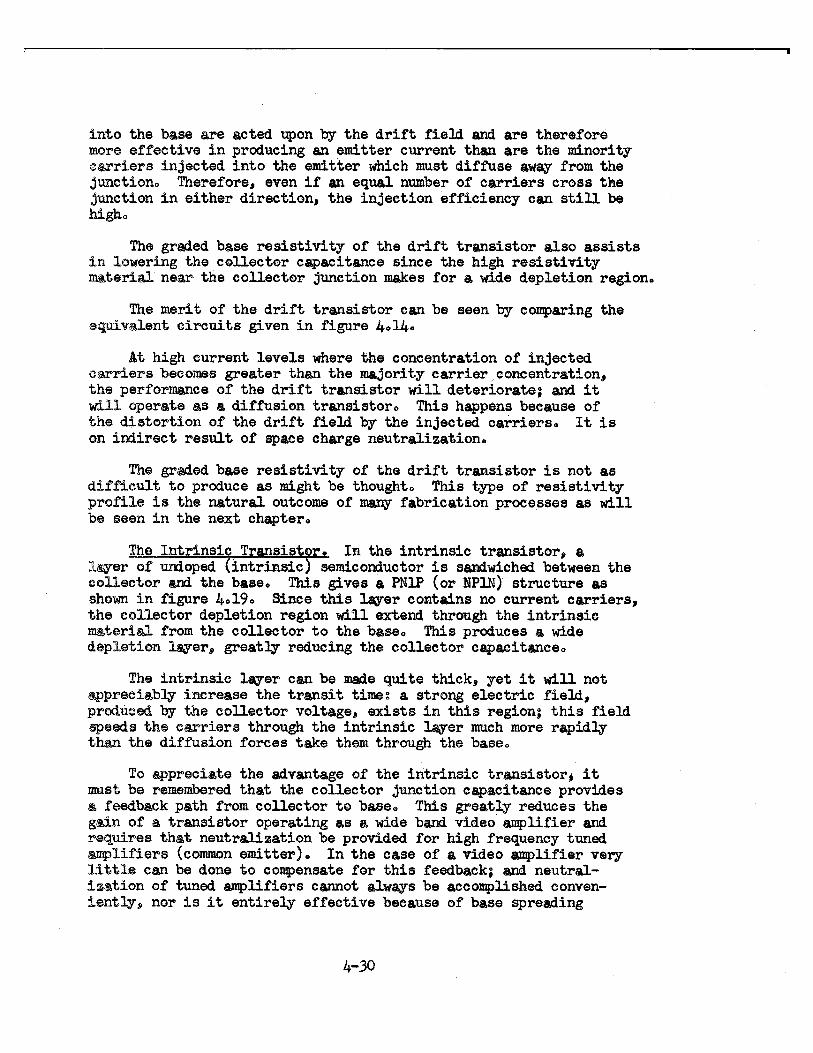
The Hook Junction Transistor» Departing new from high frequencytransistors, a junction transistor that exhibits a comon base currentgain considerably greater than one will be described,»
Ordinarily, in a two-junction transistor, the common base currentgain will approach unity, values of 0°? to O»99 being common» In theavalanche transistor which is a junction transistor operating with thecollector junction near avalanche breakdown, the comon base currentgain will be about 5 because of carrier multiplication in the col-lector depletion region. The hook junction is capable of giving ’
common base current gains in the order of 100. ' Y
The hook junction transistor enloys a PNPN (or_NPNP) structureas shown in figure &@2O. Connection is made to the emitter, base,end collector; but the P region between the base and collector isleft electrically floating. Furthermore, both center layers arethin in comparison to the diffusion length in the material, and theresistivity of these layers is considerably higher than that ofeither the emitter or the collector.
The biasing arrangement for a hook junction transistor is shownin figure h@2lo The center junction is reverse biased; the emitterand base function as usual» When the emitter junction is forwardbiased, holes will be injected into the base and will diffuse to thereverse biased center junction. The holes will then be swept intothe floating region. These holes will not be free to diffuse intothe collector since the collector junction is not fornard biasedand e barrier to holes still exists, However, the collector junctionwill become forward biased as the hole concentration in the floatingregion increases, since the excess holes make the floating regionpositive with respect to the collector» This forward bias willenable some of the holes to diffuse into the collector, and itwill also permit electrons from the collector to diffuse into thefloating regions (Note: these electrons will not eliminate theforward bias on the collector junction; enough holes will beretained in the floating region to maintain a forward bias condition.)
4-32

KIM ' 73
EMITTER Pomf CONTACT L COL\£cTOR POINT UJNTAKT
..<»oo\
‘P N
é Q/J 7
‘N -TYPE spas
BASE CONTACT
0. Possible S+rud'ure Produced by Forming Process.
./ ""=
..5
NTG-AN
-F
commonem.cukks
"NU1
’ Q» $5 Lb |.'5 130 2'-5
b Curren+ Gain Be¥ore
Figure 4.22. The Po'm+
4:)?‘
‘*0441/
”c:
... - BEFORE FORMING '
cou.:c'r0R ‘ cuRRt-:m- .
and A¥+er Forming.
Confad Tmn$\s’ror.
11--33

These electrons will diffuse across the floating region to the centerjunction and will be swept into the base. Hence, a collector currentwill be produced both by the holes leaving the base ad by the electronsswept into the base. It remains to be shown that the electron currentis very much greater than the hole current, which would indicate thatthe collector current is much greater than the emitter current.
Since the concentration of electrons in te collector is consid-erably greater than the concentration of holes in the floating region,the number of electrons crossing the collector junction will greatlyexceed the number of holes. Furthermore, since the width of thefloating region is less than the diffusion length for holes in thecollector, the diffusion current produced by a given number of electronstwill be greater than the current produced by an eqal number of holes,(see section on injection efficiency). It can be seen, then, thatthe total collector current will be much larger than the originalemitter current producing it. . »
Although some of the electron current reaching the base from thecollector do produce an emitter current, the inrease in emittercurrent will be small. The diffusion of electrons across the emitterjunction is inhibited by the remaining barrier even though thisjunction is forward biased. The electrons are preferentially sweptout the base terminal because no barrier exists.along this path.
The hook junction transistor has not seen much application. Thebiggest reason for this is probably the difficulty encountered inproducing such a device. It is not easy to obtain reproducableresults in two junction units on a production basis, and the prob-rlems associated with a multiple junction transistor can be expectedto be considerably greater.
The Point Contact Transistor. Although the point contact tran-sister was the first to appear, its operation never has been wellunderstood. A point contact transistor is made by bringing two fine,pointed wires into contact with the surface of a_N+type semiconductorwafer, the spacing between the wires being in the order of 0.001 inch.The contact between these wires and the semiconductor is a rectifyingjunction, and it is supposed that the emitter injects minority,carriers into the base which diffuse to the collector. This expla-nation is very similar to that for a junction transistor, exceptthat one irregularity exists: the common base current gain of apoint contact transistor is usually greater than one. This is notin agreement with junction transistor theory.
The explanation most frequently offered to explain the highcurrent gain of,a point contact transistor is that a hook collectoris created during a forming process. The forming process usuallyconsists of heating the collector point to a very high temperature
4»-34
. P TYPE ALI-0! IMITTIR P-TYPE ALI-QY EMITTER
Mm us: :uN\'Ac1'J? urwsau N-TYP€_ ms0- I
%_,_ F-TYPE MATEIIM. O05
W?
1*
a/us: cum-ACT
»~\ mucosa N-WM‘ am:
w TYPE Manna;
. u~1"¢E~ ALLOY Cb\-\-ECIOR _ -“gm. <9"-mar ~
ct. PNPN Tnode. b. PNPM Triode
Figure 4.23. Cons’rruc’r’|on( oY +he PNPN and PNPM Thgrokron Trar‘\sis+or.s.
+1
PM-D\N(r
ON KEHON
Cl) RRENT ""' \ \ \
BME OPENCl KUNTED
Pl-<—
\ RE<rENERAT\VE REMON\ \PEAK \~_lVEE JN I-S
‘ VDLTLGE
"V I I I +\/
-I
Figure 4.24. Breakdown Chara(+eri§’rics 0% a Tlwgrcfrron Trans'\_s\'0r, Base
Open Circulfed.
4-35
EREAKOVERvoL.1-A0!-:
U’ 1
for a short period of time. It is believed that this causes theconversion of the N—type base material near the collector junctioninto a hook structure as shown in figure A.22. This seems plausibleconsidering the current gains obtained before and after forming(figure 4.22) and considering that the impurities containd in thecontact points greatly affect the results obtained.
it the present time the point contact transistor is consideredobsolete. Shock and vibration can cause large changes in theelectrical characteristics since it is difficult to fix the positionof the contact points. Furthermore, the wide variation in theperformance of inividual units of the same type makes directreplacement of defective units impossible. Generally speaking,far superior performance can be obtained with grown junctiontransistors.
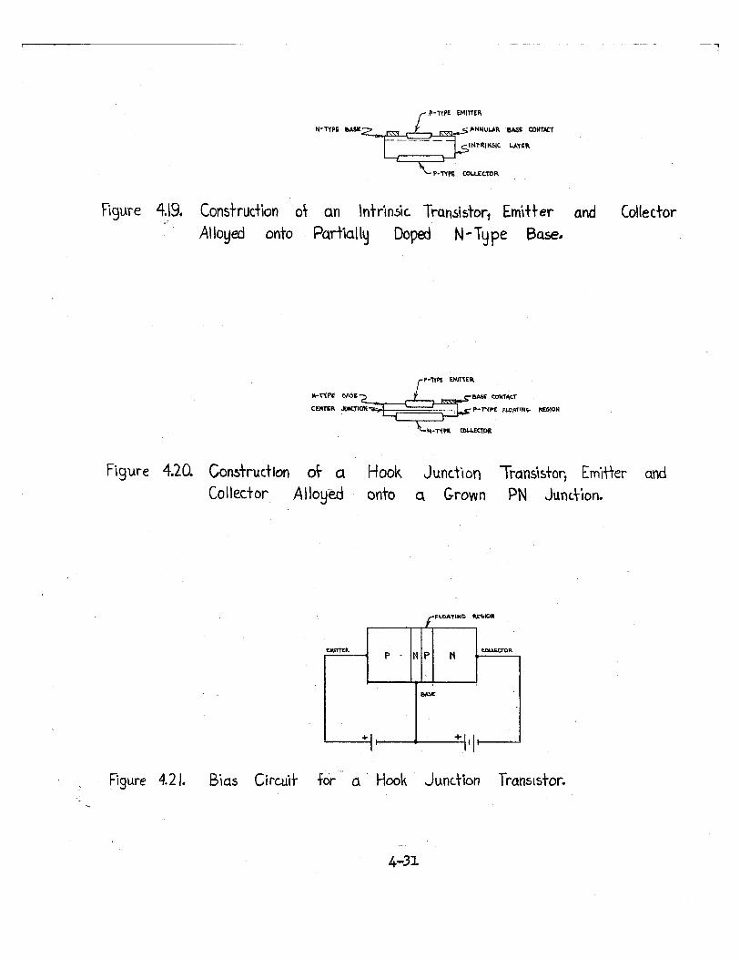
The Thyratron Transistor. Solid state devices have been builtthat display characteristics similar to those of a gas thyratron.These devices can be switched from a high resistance state to alow resistance state by a relatively small trigger signal. Inaddition, the solid state thyratron can also be turned off by thecontrol signal.
One type of thyratron transistor has a PNPN structure similarto that of a hook junction transistor. This is shown in figureh.23a. A thin, high resistivity P-type base is diffused into aN-type crystal which also has a high resistivity. A N—type col-lector is alloyed to the P-type crystal, and a P—type emitter isalloyed to the diffused layer. Hence, both the emitter and thecollector have a low resistivity. An ohmic contact is includedon the base which is made very thin to give a fast switching action.The floating P region is made relatively thick, but its width(0.005 inch) is still small in comparison to the diffusion lengthof minority carriers in the material.
The operation of the thyratron transistor can best be describedby considering its breakdown characteristics when a voltage is appliedbetween emtter and collector, reverse biasing the center junction,and the base is left open circuited.
For voltages less than the breakdown voltage, the transistorwill not conduct because of the blocking action of the center junc-tion. This condition is represented by the off region in figure4.2h. However, when the breakover voltage is reached, the currentwill increase abruptly due to avalanche multiplication of the smallreverse current through the reverse biased center junction. Theholes and electrons generated in the center junction by avalanchemultiplication will be swept into the central P and N regions bythe barrier field. These carriers cannot diffuse across the collector
4~36

IO' HO‘ D\N(_- Icvanur
<,ou_z1LTORcufueawrmm
~/
8?
uazsmunuRRENTi _
_ _ _ _ _ _ _ __g_______
6-~11--—-~~ ———— __\\ \ \\ \ \
\50~ viii" I
n.
— — - — - - _ __s»:o
-_ L°°_ . -___—___ *__ <__
2' lo; ”—"
usscvssam =so|w.Y7 ‘
' c s 1° 5 no \'s z‘o as $0 isEM|1"fE.R—¢.O\z=E£‘TDR vo\:rAea (vain)
Figure 4.25. Turn On C\'idrac\'er‘\s¥\s oi’ <1 Tgrcron TrQns'\5\'or.
CURRENT
52
£5
Figure. 4.16. Vol+—Amper-e Curve X-or ‘rhe Injed-ing Conhldr on a PNPM Thg|ra‘rron
. /// *
> //
// I/ ommc +
ELECTRON maacnou gem“; / <°"'”'Tasmcouuucrov.
W Icovfgcr ann\\\\\\\\ Y
- - -- PoLAR\‘rY As suovm
---—-— mLAR\'rY Revzksin
x a I 1
'0 0.1 0.1 O3 Q-4VOLTAGE (v,>u=\ ‘
Transisfor {'0r Bo+h D'\r'ec+ions 0% Curren+ Flow
4-3'7

and emitter junctions because of the barriers existing there so theywill set up a charge unbalance which reduces these barriers and for-ward biases both the collector and emitter junctions. Hence, theemitter will inject holes into the base which diffuse to the centerjunction. Likewise, the collector will inject electrons into thefloating N region which will also diffuse to the center junction.This makes available at the center junction a far greater number ofcurrent carriers than are required to sustain the avalanche break-down. Therefore, the voltage across this junction decreases withincreasing current. This situation is represented by the regenerativeregion in figure h.2h. The voltage will continue to fall until thedrop across the transistor is equal to that required to forward biasthe emitter and collector junctions and make up for the ohmic lossesin the material. In this condition, the device exhibits a very lowresistance.
The thyratron transistor will remain in this conducting stateuntil the current through it falls below the holding current. Whenthis happens, the number of excess carriers in the central P and Nregion will be insufficient to forward bias the emitter and col-lector junctions so the transistor returns to the nonconductingstate. ’
When a PNPN triode is in the off state, a small current doesflow. This is the saturation current of the reverse biased centerjunction» This small current will produce a charge unbalance in thecentral P and N regions which forward biases the emitter and col— .
lector junctions, permitting the injection of carriers. However,these injected carriers will become trapped in recombination centersin the central P and N regions (i.e. crystal imperfections such asmissing atoms in the lattice). As long as the carriers are notinjected faster than the trapped carriers recombine, very few willreach the center junction; and the device will not switch into theconduction state. After the current reaches a certain level, therecombination centers become saturated. Then the injectd carrierswill diffuse to the center junction producing a drop in its resist—ance, switching the transistor into the on state. ‘
If the emitter—collector voltage is less than the breakover '
voltage, the PNPN transistor can be switched on by applying atrigger signal to the base that forward biases the emitter junction.Holes will then be injected into the base and will diffuse to thecenter junction, producing a-collector current. If a large enoughtrigger is applied, the collector current will increase above thethreshold value; and the collector will inject enough carriers intothe floating region to saturate the recombination centers so thetransistor will switch on.
ii
4
omu ‘
E
> DRMN
N-TYPE BAR
P-‘NP: BénSVRROUN NNGam
N -TYPE
-_ _~G-ATE -
C-ATE
'uCHANNEL
_---
_ - 1 ~ - - -ntFLE'r\0N
RESIONS
Sm, RC; 1 ' sounc
_ +
61- Consh-ucon 0% +he F\'e\d{.E-Hec? b-Narrowmg o& channe\ by Deplei-ionTmnslskor. '
(ATE
Reguons-
_
GATE YOLW = DY
8 __
N -TYPE
1']._/"‘
URRENT(ma)
0‘
__ - -5"/'J \,
c
C->
RI-HON5
DRAN
1_.
'30 ,
SOURCE -15 _- ._ 1 2 x 1 r||"' ||||"' Q 20 Jo Q0 39 mo no noURN N‘ VOLTAGE (vol+.s\
0- Dis+or~\-um o Deplehon Region ‘ d. Charad'eri$+ic Curves.bg Drain‘ Volmge.
Figure 4.27; The F\e\d F_%¥ec’r Transis¥or-
1+-39
Figure 4625 gives the turn on characteristics of a thyratrontransistor; The characteristics are similar to those of an ordinaryjunction transistor as long as the collector current is below thethreshold l9V3l¢ When collector injection starts, the transistorbecomes regenerative and switches one
If a reverse bias is applies to the emitter—base junction, the '
injection of holes by the emitter will be stoppede When this happens,holes will no longer be swept across the center junction into thefloating region; and the forward bias on the collector junction willdrops Collector injection will then fall off, and the transistor willbecome nonconducting.
' The PNPM transistor show in figure h.23b differs from the PNPNtransistor in that a metal-semiconductor contact is used as the col~l9@tDPo As long as the collector current is below a certain value,
T
the metal contact is ohmic; and the device operates as a PNP tran—5i$tQPo However, when the current through the metalic contact isincreased above a certain level, it injects electrons into the floatingP region as would a N-type collector. ‘hen this happens, the PNPMtriode will switch into a low resistance state.
The threshold current of the PNPM transistor is determined bythe characteristics of the injecting metal contact, not by the presenceof recombination centers in the floating P region» when a currentis reached where the metal contact begins injecting, the transistorswitches_onQ
The volt-ampere characteristics of the injecting contact aregiven in figure A826. The contact has a low resistance to currentin either direction» However, at high currents, when the semi-conductor is positive with respect to the contact, the contact isno longer ohmic; but it displays a sharp drop in resistance withincreasing current. This is caused by the injection of electronsinto the semiconductor from the metals
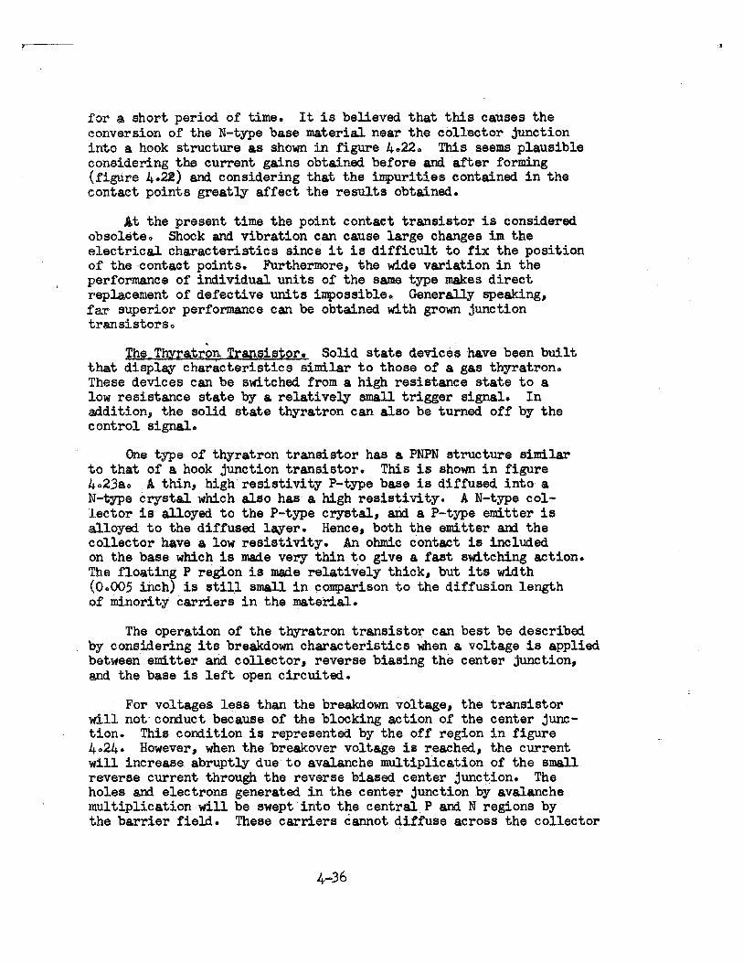
The Field Effect Transistor. The construction of the fieldeffect transistor is shown in figure hs27a; A small, high resistivityNetype bar is surrounded by a belt of low resistivity P-type materialsOhmic contacts are made to both ends of the bar and to the P~typebelts
hen this PN junction is reverse biased as shown in figure A¢27b,the depletion region will extend primarily into the bar because ofits high resistivitye Therefore, the bias on this junction cancontrol the resistance of the bar by modulating the width of theconducting channel between the depletion regionsa Hence, if avoltage is placed across the bar as shown in figure A=27c9 theresulting current can be controlled by the junction bias»
‘4P49
,’ '\
1
BAR
+ \ +
M5
1 1 1 x~_ 5 |o \5 20
UPPER use cumcr
- P-TYPE mow UMTTERQ ‘N-TYPE
7 \-bwlk BASE CONTKT
<1. Cons'\'r\Ac+‘\or$
AC1‘ViTl?-FM
—<
NJECIEDROI-F5
_ 2°‘,
I5‘-
(vo+3)\.TAC+E
5EMTTERvu
U! ,-
,§,\°
9°“~<6‘(as
\9
¢
",_...»--_ __ r.¢__,_.--l__,_ iEMITTER “CURRENT tma.)
b. Biasing Arrangemen-\’ ¢. Chc\ro\c+er|s+k Curve.
Figure 4.7.8. The Doub\e Base Diode , Diagrams and C\?arac+eris+\cs.
1+-41
Y

The electrical characteristic of the field effect transistor areshown in figure 4,27d, It can be seen that increasing the reversebias on the gate will lower the drain current by decreasing the channelwidth.
' -
At low drain voltages, the drain current increases linearly withvoltage. This is to be expected because of the resistive nature ofthe bar. However, as the drain voltage increases, the drain currentapproaches a constant value. _This happens because the voltage droppedin the chnnel will produce an additional reverse bias on the gatejunction, decreasing the channel width, This action tends to keepthe drain current constant, Since the channel becomes more positivetoward the drain terminal, widening of the depletion region will takeplace near the drain, producing the distortion shown in figure 4.27s.
The electrical characteristic of the field effect transistorare similar to those of a vacuum tube. The input impedance is high(5c,ooc-2oo,o ohms) because the gate junction isreverse biased;cFnthernore, the curves shown in figure 4.27d resemble those of avacuum pentode. '
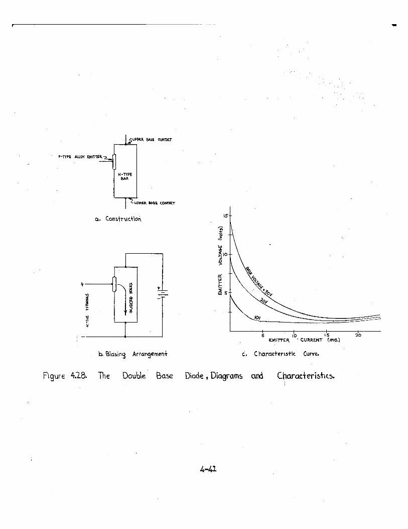
ihe Double Base Diode‘ The double base diode is a regenerativeswitch that has found application in relaxation oscillator circuits.It is made by alloying a P-type emitter to a high resistivity N-typebar which has omic contacts attached to both ends.c This config-uration is shown in figure 4.28s,
;In operation, a voltage is applid between the two base terminals,positive on the upper base as shown in figure 4,28b. This voltage willbe distributed evenly along the length of the bar, so that portion ofthe bar near the emitter junctio will be at some voltage less than theupper base voltage. .Therefore; when the active terminals are shortedtogether (emitter to lower base), the emitte junction will be reversebiased. ‘If now a positive voltage is applied to the emitter, the ‘
reverse bias will be rdnced; and if the emitter voltage becomesgreater than the voltage on the bar near the junction, the sitterwill becoe forward biased and inject holes into the bar. These holeswill be swept toward the lower base by the interbase electric field,lowering the resistivity in the region below the emitter, .Hhen thishappens, the voltage distribution along the bar is altered, the lowerportion of the bar becming less positive because of its reducedresistance, .Hence, the forward bias on the emitter is increased;and more carriers are injected. This regenerative action continues sothe current will increase until the mitter voltage drops to a lowvalue. This;produces the negative resistance mitter characteristicspshown in figue 4,280,
If the emitter voltage is reduced while the device is in the onstate, the number of injected carriers will decrease; and the resist~ance of the region below the emitter will increase. This will decreasethe forward bias on the emitter so another regenerative cycle willbegin, and the device will turn off.
4~42
Related Documents


