ELEKTRONIKOS ĮTAISAI 2009 VGTU EF ESK [email protected] 1 Transistors 1947: W.H.Brattain and J.Bardeen (Bell Labs, USA)… J.P.Pierce (Bell Labs): tran(sfer)+(re)sistor = transistor. 1949: W.Schockley theoretically described bipolar junction transistor. 1956: Nobel Prize.

Welcome message from author
This document is posted to help you gain knowledge. Please leave a comment to let me know what you think about it! Share it to your friends and learn new things together.
Transcript

ELEKTRONIKOS ĮTAISAI 2009
VGTU EF ESK [email protected]
1
Transistors
1947: W.H.Brattain and J.Bardeen (Bell Labs, USA)…
J.P.Pierce (Bell Labs): tran(sfer)+(re)sistor = transistor.
1949: W.Schockley theoretically described bipolar
junction transistor.
1956: Nobel Prize.


ELEKTRONIKOS ĮTAISAI 2009
VGTU EF ESK [email protected]
3
The first transistor was invented at Bell Laboratories on December 16,
1947 by William Shockley (seated at Brattain's laboratory bench), John
Bardeen (left) and Walter Brattain (right). This was perhaps the most
important electronics event of the 20th century, as it later made possible
the integrated circuit and microprocessor that are the basis of modern
electronics.
Transistors


ELEKTRONIKOS ĮTAISAI 2009
VGTU EF ESK [email protected]
6
The first junction transistor
http://library.thinkquest.org/C006224/history.html

ELEKTRONIKOS ĮTAISAI 2009
VGTU EF ESK [email protected]
7
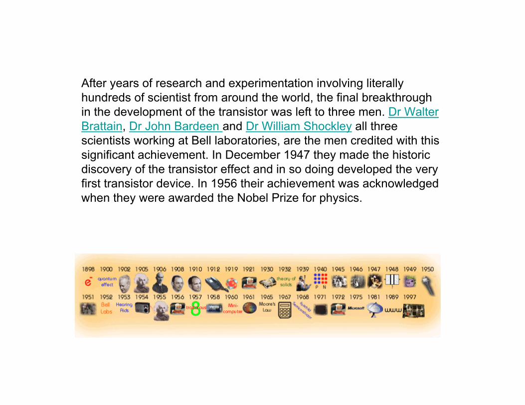
After years of research and experimentation involving literally
hundreds of scientist from around the world, the final breakthrough
in the development of the transistor was left to three men. Dr Walter
Brattain, Dr John Bardeen and Dr William Shockley all three
scientists working at Bell laboratories, are the men credited with this
significant achievement. In December 1947 they made the historic
discovery of the transistor effect and in so doing developed the very
first transistor device. In 1956 their achievement was acknowledged
when they were awarded the Nobel Prize for physics.
History
http://library.thinkquest.org/C006224/history.html
ELEKTRONIKOS ĮTAISAI 2009
VGTU EF ESK [email protected]
8
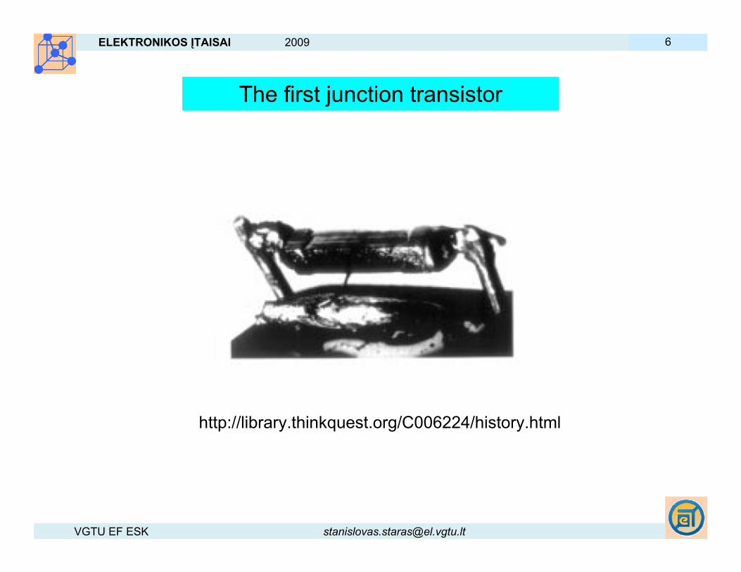
Structures and symbols of (a) pnp and (b) npn transistors
Transistors
Tran(sfer) + (re)sistor = Transistor
ELEKTRONIKOS ĮTAISAI 2009
VGTU EF ESK [email protected]
9
Transistors
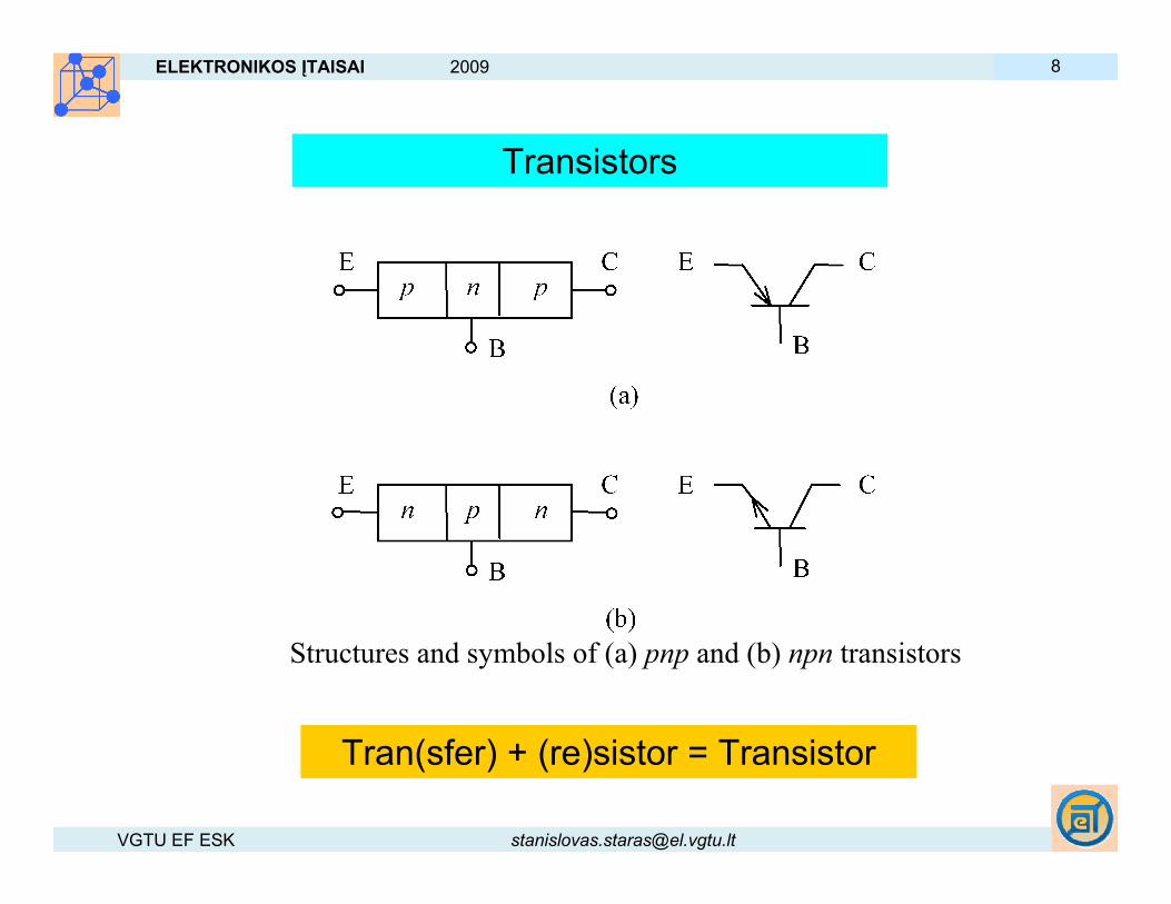
2.1. The structure and operation of a BJT
2.2. Basic configurations and modes of operation
2.3. Static volt-ampere characteristics of BJT
2.3.1. The Ebers-Moll representation of the BJT
2.3.2. Static volt-ampere characteristics
2.3.3. The real U-I characteristics
2.4. Two port representation of the transistor
2.5. Transistor models
2.5.1. T-type model
2.5.2. Π-type model
2.6. Transistor high frequency characteristics
2.7. Types of BJTs

ELEKTRONIKOS ĮTAISAI 2009
VGTU EF ESK [email protected]
11
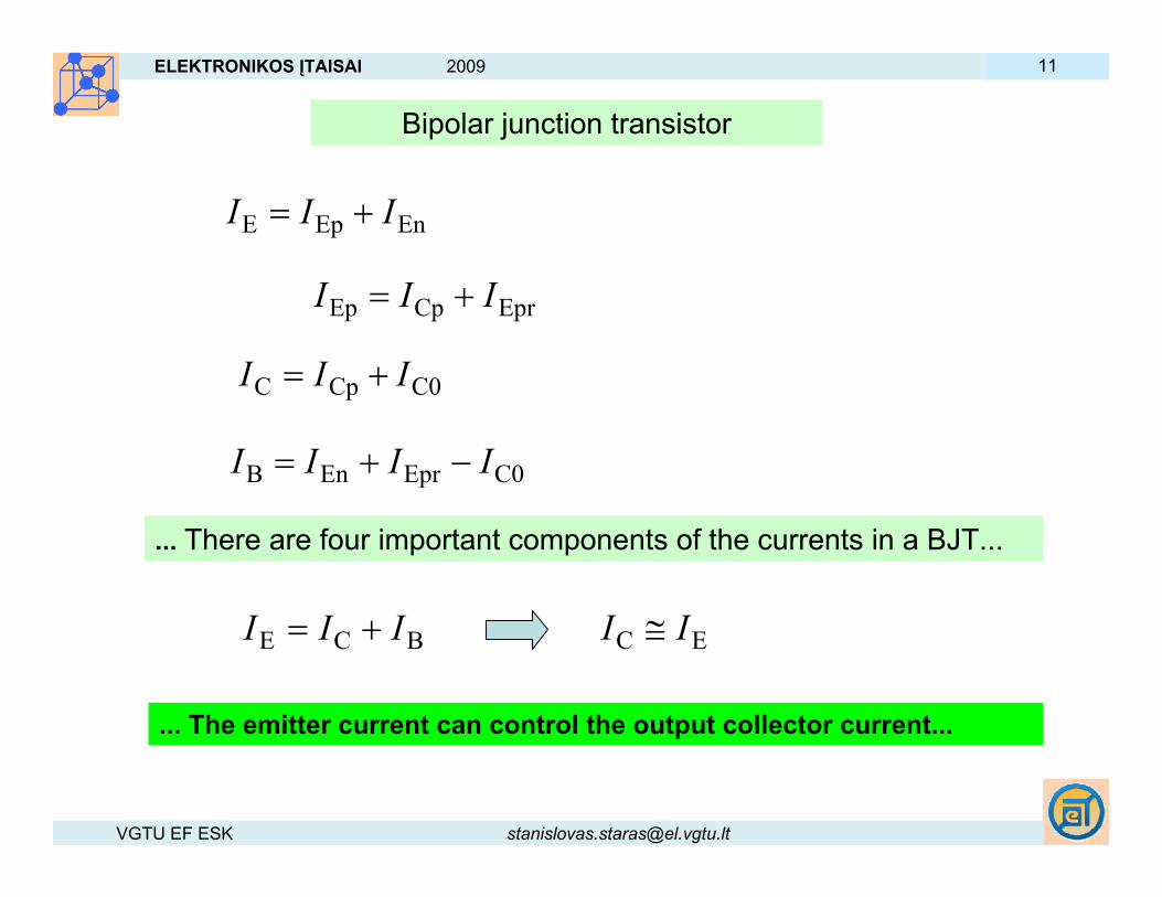
EnEpE III +=
EprCpEp III +=
C0CpC III +=
C0EprEnB IIII −+=
... There are four important components of the currents in a BJT...
BCE III += EC II ≅
... The emitter current can control the output collector current...
Bipolar junction transistor

ELEKTRONIKOS ĮTAISAI 2009
VGTU EF ESK [email protected]
12
E
Cp
I
I=Α
γδΑ ===Ep
Cp
E
Ep
E
Cp
I
I
I
I
I
I
DC current gain:
The emitter injection efficiency, is the ratio of the hole current
injected into the base from the emitter to the total emitter-base
junction current.
The base transport factor, is the ratio of the hole current across
the collector junction to that across the emitter junction.
The DC current gain can be increased increasing the main
current and decreasing other currents.
Bipolar junction transistor

ELEKTRONIKOS ĮTAISAI 2009
VGTU EF ESK [email protected]
13
Saturation
Forward-
active Cut-off
Reverse-
active
UCB
UEB
Configurations:
• Common base (CB)
• Common emitter (CE)
• Common collector (CC)
Regions of operation
Bipolar junction transistor

ELEKTRONIKOS ĮTAISAI 2009
VGTU EF ESK [email protected]
14
T
R
A
N
S
I
S
T
O
R
S
CB, CE and
CC circuits

ELEKTRONIKOS ĮTAISAI 2009
VGTU EF ESK [email protected]
15
E
C
d
d
I
IK I ==α
1d
d
EE <≅+== Α
ΑΑα
IIK I
EB
L
EEB
CL
EB
CB
d
d
d
d
r
R
Ir
IR
U
UKU α====
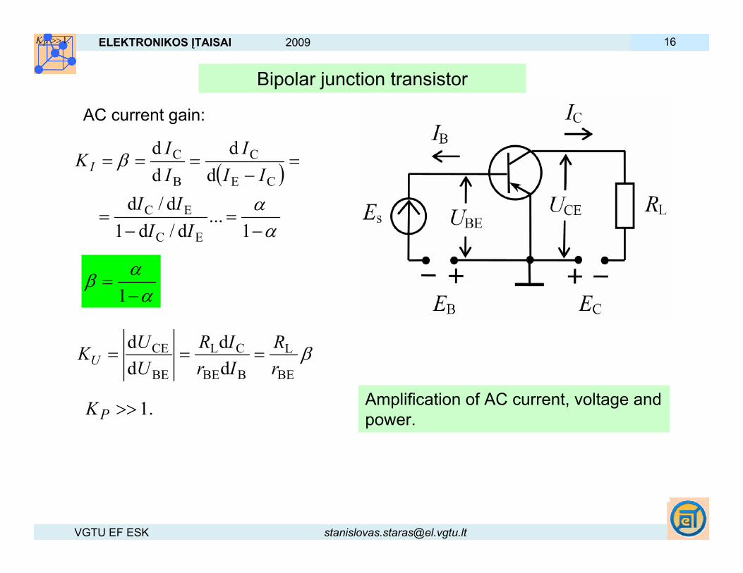
C0CpC III +=
EB
L
r
RKKK IUP ≅=
The ac current gain:
... Voltage and power amplification is possible when a BJT is in the CB
configuration.
Bipolar junction transistor
ELEKTRONIKOS ĮTAISAI 2009
VGTU EF ESK [email protected]
16.1>>PK
( )
α
α
β
−=
−=
=−
===
1...
d/d1
d/d
d
d
d
d
EC
EC
CE
C
B
C
II
II
II
I
I
IK I
βBE
L
BBE
CL
BE
CE
d
d
d
d
r
R
Ir
IR
U
UKU ===
AC current gain:
.1>>PK
α
αβ
−=
1
Amplification of AC current, voltage and
power.
Bipolar junction transistor

ELEKTRONIKOS ĮTAISAI 2009
VGTU EF ESK [email protected]
17
Gain properties of BJT
>>1>>1>>1KP
<1>>1>>1KU
>>1β>>1α<1KI
CCCECBGain
Bipolar junction transistor
ELEKTRONIKOS ĮTAISAI 2009
VGTU EF ESK [email protected]
18
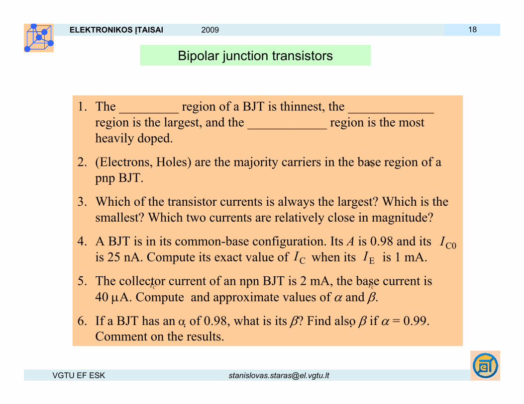
1. The _________ region of a BJT is thinnest, the _____________
region is the largest, and the ____________ region is the most
heavily doped.
2. (Electrons, Holes) are the majority carriers in the base region of a
pnp BJT.
3. Which of the transistor currents is always the largest? Which is the
smallest? Which two currents are relatively close in magnitude?
4. A BJT is in its common-base configuration. Its A is 0.98 and its
is 25 nA. Compute its exact value of when its is 1 mA.
5. The collector current of an npn BJT is 2 mA, the base current is
40 µA. Compute and approximate values of α and β.
6. If a BJT has an α of 0.98, what is its β? Find also β if α = 0.99.
Comment on the results.
CI
CI
C0I
CI EI
CI
Bipolar junction transistors
After years of research and experimentation involving literally
hundreds of scientist from around the world, the final breakthrough
in the development of the transistor was left to three men. Dr Walter
Brattain, Dr John Bardeen and Dr William Shockley all three
scientists working at Bell laboratories, are the men credited with this
significant achievement. In December 1947 they made the historic
discovery of the transistor effect and in so doing developed the very
first transistor device. In 1956 their achievement was acknowledged
when they were awarded the Nobel Prize for physics.

___trailing the Transistor History.mht
Related Documents