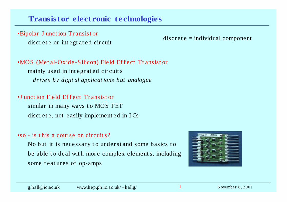
November 8, 2001 [email protected] www.hep.ph.ic.ac.uk/~hallg/ 1 Transistor electronic technologies •Bipolar Junction Transistor discrete or integrated circuit •MOS (Metal-Oxide-Silicon) Field Effect Transistor mainly used in integrated circuits driven by digital applications but analogue •Junction Field Effect Transistor similar in many ways to MOS FET discrete, not easily implemented in ICs •so - is this a course on circuits? No but it is necessary to understand some basics to be able to deal with more complex elements, including some features of op-amps discrete = individual component

Welcome message from author
This document is posted to help you gain knowledge. Please leave a comment to let me know what you think about it! Share it to your friends and learn new things together.
Transcript
November 8, [email protected] www.hep.ph.ic.ac.uk/~hallg/ 1
Transistor electronic technologies•Bipolar Junction Transistor
discrete or integrated circuit
•MOS (Metal-Oxide-Silicon) Field Effect Transistormainly used in integrated circuits
driven by digital applications but analogue
•Junction Field Effect Transistorsimilar in many ways to MOS FETdiscrete, not easily implemented in ICs
•so - is this a course on circuits?No but it is necessary to understand some basics tobe able to deal with more complex elements, includingsome features of op-amps
discrete = individual component
November 8, [email protected] www.hep.ph.ic.ac.uk/~hallg/ 2
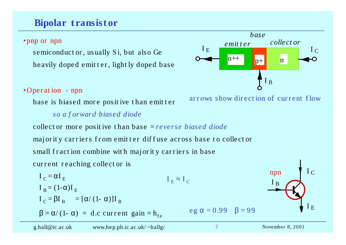
Bipolar transistor•pnp or npn
semiconductor, usually Si, but also Geheavily doped emitter, lightly doped base
•Operation - npnbase is biased more positive than emitter
so a forward biased diodecollector more positive than base = reverse biased diode majority carriers from emitter diffuse across base to collectorsmall fraction combine with majority carriers in basecurrent reaching collector is
IC = αIE
IB = (1-α)IE
IC = βIB = [α/(1- α)]IB
β = α/(1- α) = d.c current gain = hfe
p+ nn++
emitter collectorbase
IB
ICIE
IB
IC
IE
npn
arrows show direction of current flow
eg α = 0.99 β = 99
IE ≈ IC
November 8, [email protected] www.hep.ph.ic.ac.uk/~hallg/ 3
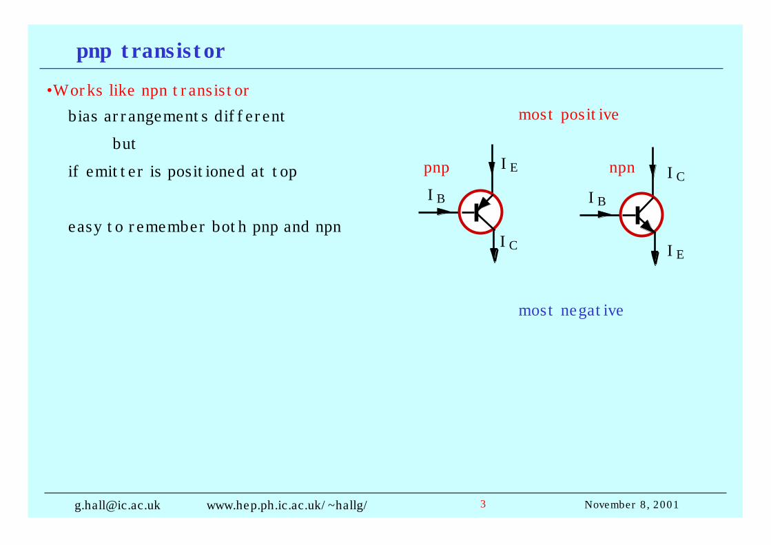
pnp transistor•Works like npn transistor
bias arrangements differentbut
if emitter is positioned at top
easy to remember both pnp and npn
most positive
most negative
IB
IC
IEpnp
IB
IC
IE
npn

November 8, [email protected] www.hep.ph.ic.ac.uk/~hallg/ 4
Slightly more precise picture•to turn npn transistor on VB-VE = VBE > 0.6-0.7V
(invert for pnp)
•so we can use it as a switch by controlling VBE
VBE ≈ 0 IC = IE = 0
•however, if transistor is ON VBE ≈ 0.7Vthis is a consequence of the diode behaviour -
discuss in a moment
•in contrast, β is not a reliable parameter for design
NB bothlog scales
2n3906 npn transistor
NB log scale for IC
IC (mA)
β

November 8, [email protected] www.hep.ph.ic.ac.uk/~hallg/ 5
Ebers-Moll model•Transistor can be modelled as two back-to-back diodes
I-V behaviour of diode I ≈ I0[exp(qVBE/kT)-1)]
•Base-emitter diode is forward biasedIE = IE0.[exp(qVBE/kT)-1] ≈ IE0exp(qVBE/kT) ie VBE ≈ (kT/q)logeIE
•Base-collector diode is reverse biasedIBC = ICO[exp(qVBC/kT)-1] ≈ IC0 - which is smallso current arriving at collector is dominated by current from emitter, which hasdiffused across base
•How does current vary with small change in VBE?dIE/dVBE = ie/vbe = (q/kT)IE0exp(qVBE/kT) = (q/kT)IE
iere = vbe with re = kT/qI = 25Ω/IE(mA)
ie to ac current signals transistor looks like dynamic resistance
this explains why VBE varies so little with Ialso basis of band-gap T reference
NB we don’t usually need todistinguish between IC andIE - consider them equal
November 8, [email protected] www.hep.ph.ic.ac.uk/~hallg/ 6
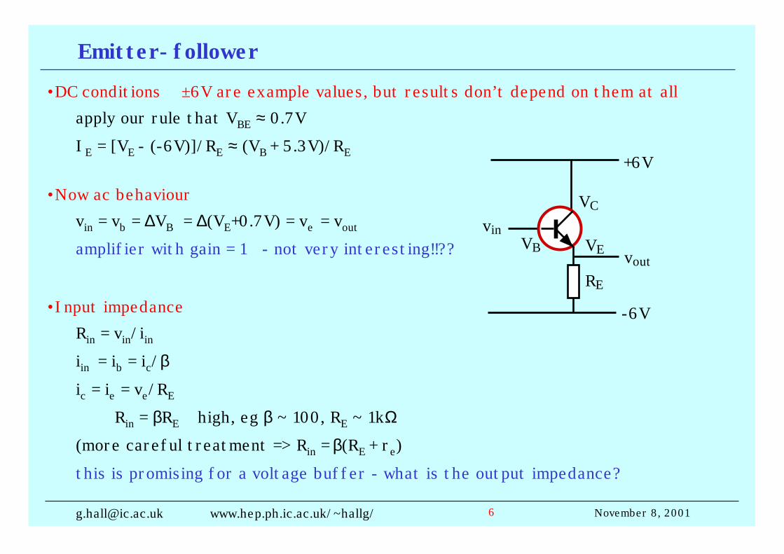
Emitter-follower
+6V
-6V
VB VE
VC
RE
vin
vout
•DC conditions ±6V are example values, but results don’t depend on them at allapply our rule that VBE ≈ 0.7VIE = [VE - (-6V)]/RE ≈ (VB + 5.3V)/RE
•Now ac behaviourvin = vb = ∆VB = ∆(VE+0.7V) = ve = vout
amplifier with gain = 1 - not very interesting!!??
•Input impedanceRin = vin/iiniin = ib = ic/β
ic = ie = ve/RE
Rin = βRE high, eg β ~ 100, RE ~ 1kΩ
(more careful treatment => Rin = β(RE + re)this is promising for a voltage buffer - what is the output impedance?

November 8, [email protected] www.hep.ph.ic.ac.uk/~hallg/ 7
Emitter-follower output impedance•How to find it? Consider the black box…
vary vout and see what happens to iout
keep other conditions fixed
•Use Ebers-Moll result VBE = (kT/q)logeIE
dVBE/dIE = vbe/ie =(kT/qIE )
•If VB is constantvout = ve
iout = ieZout = (kT/qIE ) = re = 25Ω/IE(mA)
voutRO
iout
small, as required for buffer
+6V
-6V
VB VE
VC
RE
vin
vout

November 8, [email protected] www.hep.ph.ic.ac.uk/~hallg/ 8
Short footnotes•In analysing circuits for small signal (AC) behaviour
all fixed DC levels are equivalent to groundie ac current does not need to distinguish voltage at other end of path
•This is often useful in looking at circuits to tell if routes are in parallel
•Calculationskeep simpletry to make approximations - 1% answers are almost never required
if so better tools existeg parallel resistances transistor β - assume β ≈ 100 - unless better value known or is critical 47Ω ≈ 51Ω ≈ 50Ω
November 8, [email protected] www.hep.ph.ic.ac.uk/~hallg/ 9
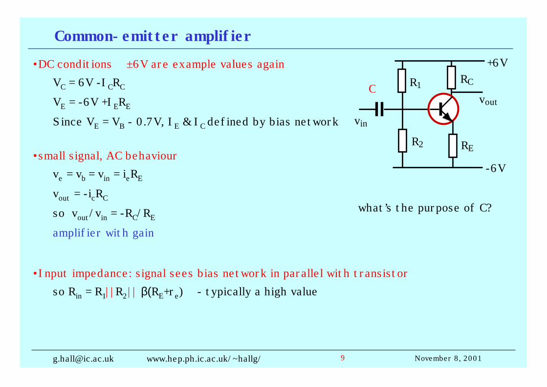
Common-emitter amplifier•DC conditions ±6V are example values again
VC = 6V -ICRC
VE = -6V +IERE
Since VE = VB - 0.7V, IE & IC defined by bias network
•small signal, AC behaviourve = vb = vin = ieRE
vout = -icRC
so vout/vin = -RC/RE
amplifier with gain
•Input impedance: signal sees bias network in parallel with transistorso Rin = R1||R2|| β(RE+re) - typically a high value
+6V
-6V
RE
vin
vout
RC
R2
R1C
what’s the purpose of C?
November 8, [email protected] www.hep.ph.ic.ac.uk/~hallg/ 10
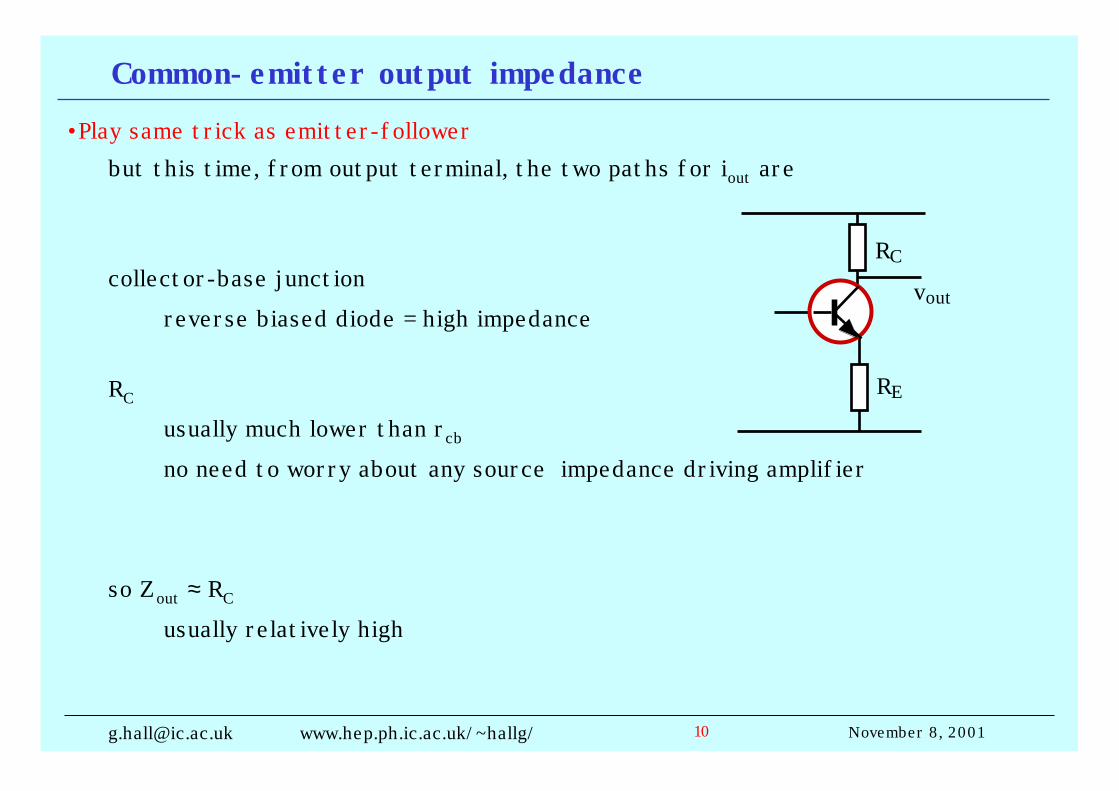
Common-emitter output impedance
RE
vout
RC
•Play same trick as emitter-followerbut this time, from output terminal, the two paths for iout are
collector-base junctionreverse biased diode = high impedance
RC
usually much lower than rcb
no need to worry about any source impedance driving amplifier
so Zout ≈ RC
usually relatively high
November 8, [email protected] www.hep.ph.ic.ac.uk/~hallg/ 11
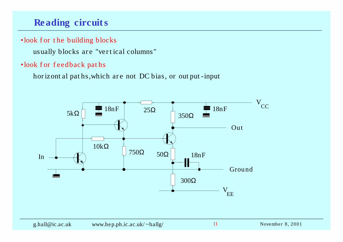
Reading circuits
CC5kΩ
10kΩ750Ω
25Ω350Ω
50Ω
300Ω
18nF
18nF 18nF
Out
In
Ground
VEE
V
• look for the building blocksusually blocks are "vertical columns"
• look for feedback pathshorizontal paths,which are not DC bias, or output-input
November 8, [email protected] www.hep.ph.ic.ac.uk/~hallg/ 12
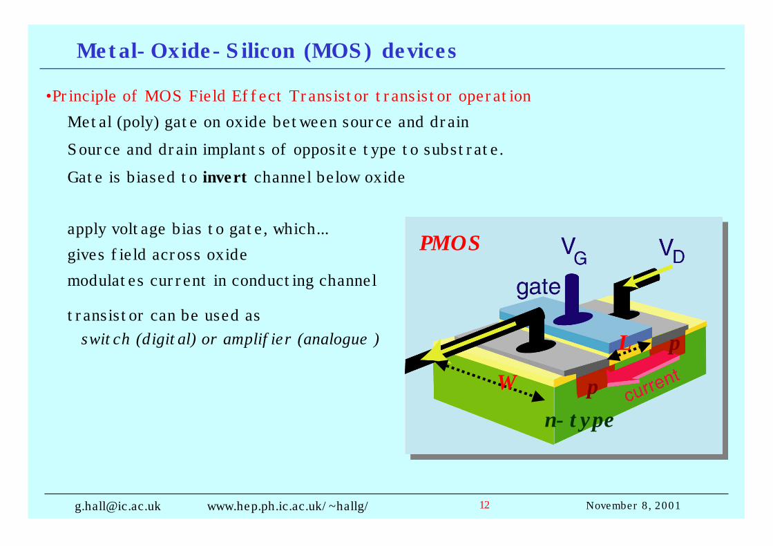
Metal-Oxide-Silicon (MOS) devices
•Principle of MOS Field Effect Transistor transistor operationMetal (poly) gate on oxide between source and drainSource and drain implants of opposite type to substrate.Gate is biased to invert channel below oxide
apply voltage bias to gate, which...gives field across oxidemodulates current in conducting channel
transistor can be used asswitch (digital) or amplifier (analogue )
W
L
n-typep
PMOS
p

November 8, [email protected] www.hep.ph.ic.ac.uk/~hallg/ 13
MOS Field Effect Transistor•Operation - input signal is voltage on gate
very high input impedance > 1012Ω
•I-V behaviour nMOS VG > VT to switch on, vary VDS
linear regionIDS ~ (VG - VT)VDS
saturation region channel “pinch off” near drain
IDS ~ (VG - VT)2
∂IDS/∂VGS = ids/vgs = gm = (2µCoxIDSW/L)1/2 transconductance
defined by geometry & current only - important for IC design
n-FET
p type
drainsourcegate
n type
depleted region
oxide
inverted channel
substrate
G
D
S
IDS
bodypMOS
G
D
S
bodynMOS

November 8, [email protected] www.hep.ph.ic.ac.uk/~hallg/ 14
Designing with MOSFETs
2SK3019 small signal switching
•Mostly operate in saturation - choice of gate-source voltage determines currentbut often bias with current source, so gate voltage "selected by" current
saturationregion
linearregion
in saturation
region
slope gm
November 8, [email protected] www.hep.ph.ic.ac.uk/~hallg/ 15
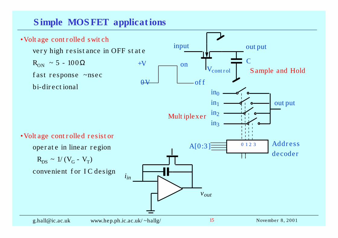
Simple MOSFET applications•Voltage controlled switch
very high resistance in OFF stateRON ~ 5 - 100Ω
fast response ~nsecbi-directional
•Voltage controlled resistoroperate in linear region RDS ~ 1/(VG - VT)convenient for IC design
input
0V
+V
off
on
output
VcontrolCSample and Hold
Multiplexer
0 1 2 3 Address decoder
A[0:3]
outputin0in1in2in3
vout
iin

November 8, [email protected] www.hep.ph.ic.ac.uk/~hallg/ 16
ElectroStatic Discharge•MOS circuits are prone to damage from ESD
gate oxides are thin layers - few nm in advanced technologiesoxide breakdown field < 1000MV/m = 1V/nm
•Human body can easily charge to 30-40kV walking across carpet on a dry dayprecautions:circuits designed with protection diodesstand on conductive pad and earth body with wrist strap
4000V ESD test
November 8, [email protected] www.hep.ph.ic.ac.uk/~hallg/ 17
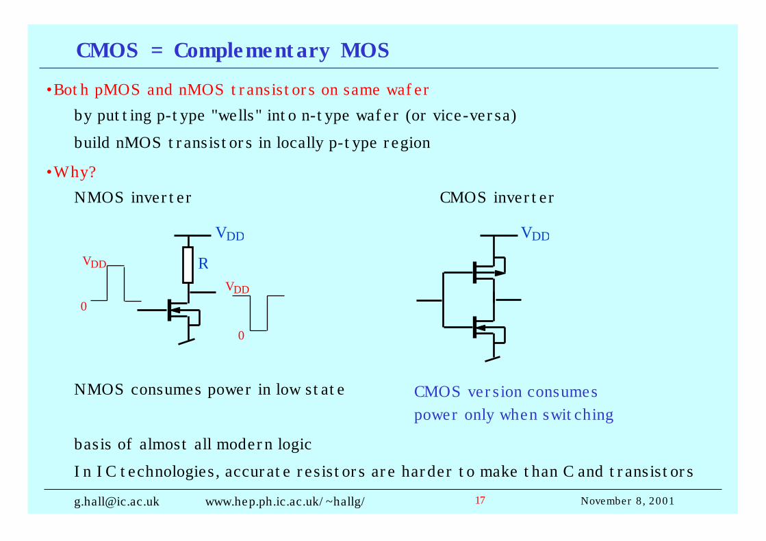
CMOS = Complementary MOS•Both pMOS and nMOS transistors on same wafer
by putting p-type "wells" into n-type wafer (or vice-versa)build nMOS transistors in locally p-type region
•Why?NMOS inverter CMOS inverter
NMOS consumes power in low state
basis of almost all modern logicIn IC technologies, accurate resistors are harder to make than C and transistors
VDD
RVDD
0VDD
0
VDD
CMOS version consumespower only when switching
November 8, [email protected] www.hep.ph.ic.ac.uk/~hallg/ 18
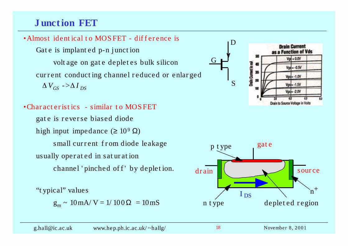
Junction FET•Almost identical to MOSFET - difference is
Gate is implanted p-n junctionvoltage on gate depletes bulk silicon
current conducting channel reduced or enlargedVGS -> IDS
•Characteristics - similar to MOSFETgate is reverse biased diodehigh input impedance (≥ 109 Ω)
small current from diode leakageusually operated in saturation
channel 'pinched off' by depletion.
“typical” valuesgm ~ 10mA/V = 1/100Ω = 10mS
G
D
S
n type
drain source
gatep type
depleted regionIDS n+
November 8, [email protected] www.hep.ph.ic.ac.uk/~hallg/ 19
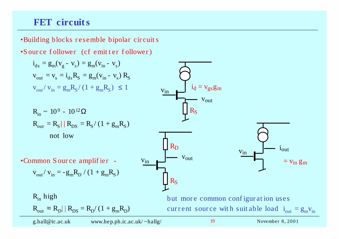
FET circuits•Building blocks resemble bipolar circuits•Source follower (cf emitter follower)
ids = gm(vg - vs) = gm(vin - vs)vout = vs = idsRS = gm(vin - vs) RS
vout/vin = gmRS/(1 + gmRS) ≤ 1
Rin ~ 109 - 1012Ω
Rout = RS||RDS = RS/(1 + gmRS)not low
•Common Source amplifier -vout/vin = -gmRD /(1 + gmRS)
Rin highRout ≈ RD||RDS = RD/(1 + gmRD)
id = vgsgm
RS
vout
vin
RS
vout vin
RD
= vin gm
iout vin
but more common configuration usescurrent source with suitable load iout = gmvin

November 8, [email protected] www.hep.ph.ic.ac.uk/~hallg/ 20
FET limitations•On Resistance
although small, it contributes to RC time in fast switches
•Capacitanceinevitable capacitances between nodes, important for high speed circuitsCgate ~ CoxWL for MOSFETs
•Relevance to op-ampsFET amplifiers have much higher input impedance
and draw much lower currents
•Cautions•Latch-up
under certain conditions, parasitic bipolar transistors formedMOS circuits can go into high current states - destructive
•ESDcare needed in handling
protection networks can degrade performance

November 8, [email protected] www.hep.ph.ic.ac.uk/~hallg/ 21
Another building block - the current mirror (if time)•Q1 & Q2 are identical transistors
VBE1 = VBE2 and VBE ≈ (kT/q)logeIE
so Iout = Iref
widely used in ICs where closely matched transistorsare easy to construct - useful to program currents
•add a resistorIout =(kT/qR)loge(Iref/Iout)eg R = 1kΩ, Iref = 1mA => Iout = 67µA
• add another resistorVBE1 ≈ VBE2
I1/I2 = R2/R1
also works for discretecircuits
R1 R2R
Rload

November 8, [email protected] www.hep.ph.ic.ac.uk/~hallg/ 22
Band-gap circuit•To be more precise,
VBE ~ log(current density) so in non-matched transistorswith same current, and ratio of emitter areas rVBE1-VBE2 = (kT/q)ln(r)
easy to achieve in IC technology
•Principle of AD590 T sensorProportional To Absolute Temperature (PTAT)I1 = I2
∆ VBE = (kT/q)ln(r) = I1RI = I1 + I2 = (2kT/qR)ln(r) r = 8 R ≈ 1kΩ
I ≈ 1µA/K @ 300KR should vary little with T
•actual AD590 only slightly more complicated
+
-R
I1 I2
I
r 1
11
AD590 precision
November 8, [email protected] www.hep.ph.ic.ac.uk/~hallg/ 23
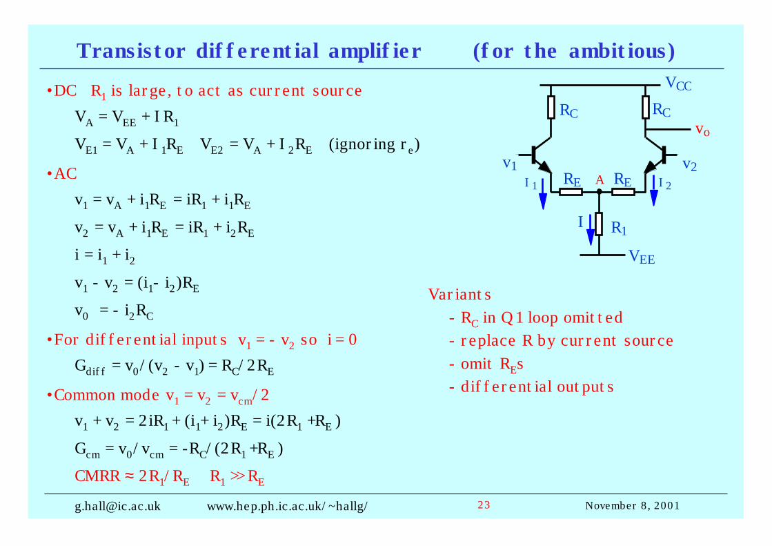
Transistor differential amplifier (for the ambitious)•DC R1 is large, to act as current source
VA = VEE + IR1
VE1 = VA + I1RE VE2 = VA + I2RE (ignoring re)
•ACv1 = vA + i1RE = iR1 + i1RE
v2 = vA + i1RE = iR1 + i2RE
i = i1 + i2v1 - v2 = (i1- i2)RE
v0 = - i2RC
•For differential inputs v1 = - v2 so i = 0Gdiff = v0/(v2 - v1) = RC/2RE
•Common mode v1 = v2 = vcm/2v1 + v2 = 2iR1 + (i1+ i2)RE = i(2R1 +RE )Gcm = v0/vcm = -RC/(2R1 +RE )CMRR ≈ 2R1/RE R1 >> RE
R1
I1 I2
I
RC RC
RERE
vo
v2v1
VCC
VEE
A
Variants- RC in Q1 loop omitted- replace R by current source- omit REs- differential outputs
November 8, [email protected] www.hep.ph.ic.ac.uk/~hallg/ 24
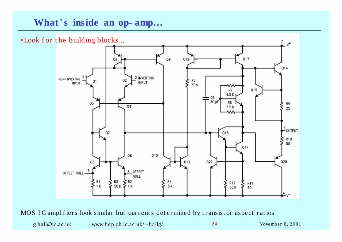
What's inside an op-amp…
•Look for the building blocks...
MOS IC amplifiers look similar but currents determined by transistor aspect ratios
Related Documents