Transistor Circuits for MEMS Based Transceiver Yuehan Xu Keli Hui Darryl Yu Soumya Mantha Kelvin Liang Electrical Engineering and Computer Sciences University of California at Berkeley Technical Report No. UCB/EECS-2015-62 http://www.eecs.berkeley.edu/Pubs/TechRpts/2015/EECS-2015-62.html May 12, 2015

Welcome message from author
This document is posted to help you gain knowledge. Please leave a comment to let me know what you think about it! Share it to your friends and learn new things together.
Transcript

Transistor Circuits for MEMS Based Transceiver
Yuehan XuKeli HuiDarryl YuSoumya ManthaKelvin Liang
Electrical Engineering and Computer SciencesUniversity of California at Berkeley
Technical Report No. UCB/EECS-2015-62http://www.eecs.berkeley.edu/Pubs/TechRpts/2015/EECS-2015-62.html
May 12, 2015

Copyright © 2015, by the author(s).All rights reserved.
Permission to make digital or hard copies of all or part of this work forpersonal or classroom use is granted without fee provided that copies arenot made or distributed for profit or commercial advantage and thatcopies bear this notice and the full citation on the first page. To copyotherwise, to republish, to post on servers or to redistribute to lists,requires prior specific permission.
University of California, Berkeley College of Engineering
MASTER OF ENGINEERING - SPRING 2015
Electrical Engineering & Computer Science Department
Physical Electronics and Integrated Circuits
MEMS-based wireless Transceiver
Yuehan Xu
This Masters Project Paper fulfills the Master of Engineering degree requirement.
Approved by:
1. Capstone Project Advisor:
Signature: __________________________ Date ____________
Print Name/Department: Clark T.-C. Nguyen/EECS
2. Faculty Committee Member #2:
Signature: __________________________ Date ____________
Print Name/Department: David Allstot/EECS

Transistor Circuits for MEMS Based Transceiver
Final Report
Written By: Yuehan Xu
Project Partners:
Kelvin Liang Darryl Yu
Keli Hui Soumya Mantha
Date:
04/15/2015

Table of Contents
I. Project Description (Group)
II. Industry Analysis and Proposed Market Strategy(Group)
III. Technical Contribution (Individual)
IV. Consolidated Paper (Group)
V. Concluding Reflections(Individual)

I. Project Description
In recent years, the push for low power wireless sensor networks has called for the
introduction of RF-MEMS transceiver devices capable of operating on scavenged power. The
design of ultra-low power MEMS based transceivers stands to revolutionize the fields of
industrial monitoring, environmental monitoring, and biomedical imaging.
This report demonstrates a MEMS based transceiver capable of supporting these low
power applications. Included are design and simulation results using transistor circuits
implemented with a commercial TSMC 180nm technology. The entire system is estimated to
consume 57.8uW of power at a Vdd=1.8V, duty cycled at 50%. The transceiver system
implements a modified OOK modulation scheme and utilizes a MEMS resonator, an oscillator,
an envelope detector, a comparator, a power amplifier, and an output buffer. The system is
currently optimized for data rates of 5kHz, but can easily support much higher data rates. This
design demonstrates operation at 60MHz VHF, but the tunable nature of the MEMS device
allows for use of frequencies up to UHF.
The remainder of this report is organized as follows. Section II explains the current state
of the industry that the transceiver is to be commercialized in. This section also uses that
information to propose a viable go-to-market strategy for a startup seeking to commercialize this
technology. Section III presents a detailed description of my individual contributions toward the
capstone project. Section IV is a consolidated paper with brief descriptions of the performance of
each individual block in the transceiver architecture. It also includes simulation results showing
the performance of the transceiver as a whole after all individual work was integrated together.
Section V finishes with concluding reflections on the progress of the capstone project and
potential directions for future work.

II. Industry Analysis and Proposed Market Strategy
This paper provides a detailed industry analysis of our MEMS transceiver chip by first
comparing against other competing technologies already present in the market and then
proposing a viable go-to-market strategy with our technology. The biggest competitors to our
MEMS-based wireless transceiver technology are WiFi, Zigbee, and Bluetooth. Therefore, we
begin by proving our transceiver technology as a viable competitor against these existing
technologies due to lower cost and lower power consumption. Despite this fact, our analysis of
the wireless semiconductor industry using Porter’s five forces will show that barriers to entry
into this industry are extremely high. We identify an alternate strategy to bring our technology to
market; we plan to vertically integrate our technology into an electrical sensing system for
agriculture. We will show that we can not only exploit the weak forces in the agricultural sensing
systems market, we can also capture most of the value chain by having exclusive access to our
MEMS technology. By entering the agricultural sensing market, our strategy is to dominate the
market by being both a chip designer and a systems manufacturer.
The objective of our capstone team is to build a fully-functional low power transceiver
chip that successfully integrates a microelectromechanical system (MEMS) resonator. We
accomplish this by creating a strict power budget of 60 micro watts for the entire system and
using block-level design methodology to implement the CMOS transistors in the transceiver
chain. We conduct this process in three steps. First, we create a schematic of our transceiver
circuit and verify its functionality in simulation. Next, we implement the layout that corresponds
to our schematic by designating the locations of connections, wires, doped wells, and metal
layers. Finally, once the chip has been fabricated, we need to use PCB boards to conduct the final
tests needed to verify its operation. These steps will allow us to achieve a low-power MEMS
transceiver chip that is ready for commercial use at the end of the year.
Before discussing about specific competing technologies to MEMS, it is important to
appreciate the context of how transceivers operate and what are some design metrics for a good
transceiver. This paper will first distinguish the power advantages of our MEMS transceiver chip
from other conventional transceivers. We will then show why these advantages are relevant by
illustrating the need for minimizing power use in today's transceiver applications.
Transceivers allow for wireless communications by transmitting and receiving wireless
signals. To avoid interference, signals traveling in the air must travel in different frequency
channels. This often requires them to be converted into higher frequencies in a process called
modulation. When the signal then reaches its destination, the receiver then needs to recover the
original signal from the modulated signal in a process called demodulation. It is the job of the
transceiver to modulate and demodulate signals being sent and received; it does this by using a
resonator to generate a reference frequency that is tuned to the desired sending or receiving
frequency of the signal.
When designing a transceiver chain, the most difficult problem is isolating the desired
signal from other unwanted signals that are received from the antenna. Engineers define the Q
factor of a resonator as its ability to resonate at a specific frequency. Resonators with a low Q
factor are less selective; they resonate not only at the tuned frequency, but also at other nearby
frequencies. For smaller channels, the Q of the resonator needs to be high in order to minimize
insertion loss, or loss of signal strength (Nguyen, 2013, p. 112). Most conventional transceivers

implement resonators that need additional filtering to isolate the signal. This costs power.
Although we would like to fit many channels into our band, smaller channel bandwidths require
stronger filtering and consume more power.
Herein lies the advantage of MEMS technology. Mechanical resonators generate larger Q
factors than resonators using quartz crystals. MEMS resonators provide record on-chip Q factors
operating at gigahertz frequencies while still maintaining excellent thermal and aging stability
(Nguyen, 2013, p. 110). In particular, the capacitive-gap RF MEMS resonator that we use for our
MEMS transceiver circuit produces exceptionally high Q around 100,000 and can be tuned to
select 1kHz-wide channels over a 80kHz range (Rocheleau, Naing, Nilchi, & Nguyen, 2014, p.
83). The high Q factors of MEMS resonators eliminates any steps involving additional filtering
and takes away the power consumption overhead required for reducing insertion loss from the
resonator. Eliminating the filtering step also results in a simpler design for the system as a whole.
Next, this paper provides examples of applications using our low-power MEMS-based
transceiver to show its relevance in the market today. The main interests of our technology will
come from wireless sensor node markets, where low power and simplicity are much more
important than data transmission rate (Rocheleau, Naing, Nilchi, & Nguyen, 2014, p. 83). Since
the wireless sensor market is wide and diverse, this paper uses body area network (BAN) sensors
and environmental sensor networks (ESNs) as case studies to illustrate the needs for simple, low-
power transceivers.
BAN sensors are used to collect information directly from the person's body. Designers
integrate BAN sensors into smart textiles to detect the wearer's heart rate, stress, motion, and
energy expenditure (Peiris, 2013, p. 1). A transceiver chip will then enable the sensors to send
this physiological information to an interface where either the person or a medical professional

can view it and form educated decisions. The biggest challenge with these devices is
miniaturizing the BAN node and keeping it low power while maintaining a broad range of
applications. A full on-chip application-specific implementation for BAN has already been
designed using the wireless protocol Zigbee and consumes approximately 4mW of power when
transmitting and receiving. A tiny lithium coin-cell battery can easily provide enough power for
this radio. Although current implementations of BAN are functional, an approach to combine
MEMS technology with ICs has already been discussed as the next step to further miniaturize the
features of the BAN project (Peiris, 2013, p. 2). If we decreased power consumption from the
milliwatt range to the microwatt range using MEMS, the battery life will increase by several
orders of magnitude.
ESNs are another area where we can employ low-power transceivers. These sensors
constantly monitor the natural environment to study how they work and detect natural hazards
such as floods and earthquakes. The transceiver allows for communication between the sensors
and a Sensor Network Server, where it can be viewed at a base station (Hart, Martinez, 2006, p.
178). The biggest advantage of ESNs is that they allow us to monitor remote or dangerous areas
that have long been inaccessible to study (Hart, Martinez, 2006, p. 177). The designer of these
sensors needs to satisfy both low power and low maintenance constraints; these will ensure that
the system will operate with minimum intervention for sensor maintenance or changing batteries.
MEMS technology can provide the low power and simplicity needed for these sensor nodes. An
approach to build tiny cubic millimeter sensor nodes called Smart Dust using MEMS technology
has already been proposed, although environmental robustness is an additional design constraint
for this particular application (Hart, Martinez, 2006, p. 180).
We have shown that some wireless sensor applications such as BANs and ESNs need
ultra-low power transceivers. To show that MEMS is a feasible technology, we now require a
closer examination of the major competitors in wireless sensor applications. The most
recognizable competing technology in wireless communications is WiFi. WiFi is the biggest
threat to our technology because of its wide use in applications from cell phones to computers.
Because it is supported across many platforms, WiFi is even used extensively for smart wearable
and connected medical device applications. Thus, WiFi takes a sizeable chunk of the market that
we hope to apply our technology. The cost per WiFi chip is moderately expensive at a bulk price
of $3 for 1000 chips (Smith, 2011). Although this cost is slightly inflated, WiFi’s biggest
strength is that it is the fastest means of wireless communications in the industry. Supporting up
to 11 to 54Mbps (megabits per second), WiFi takes a commanding lead over the second fastest
wireless method, which is Bluetooth at 1Mbps (Smith, 2011). This means that WiFi transfers
data up to 54 times faster than Bluetooth. Our transceiver can be configured for high data rates
but at the expense of additional power consumption. Therefore, to secure a special niche for low
power and low cost, our design is not optimized for speed. We operate at speeds of 200kbps,
which is much lower than WiFi. However, the relaxed speed constraint allows us to design our
transceiver architecture to be much simpler than typical WiFi chips and less costly as a result
(Dye, 2001). By using a simple design, our MEMS-based chip is expected to be less costly at
about $2.5 for 1000 chips.This is another strength of our MEMS transceiver in addition to the
aforementioned low-power advantages from using a high-Q MEMS resonator. Although WiFi is
a major competitor in the wireless communications field, low power applications that do not
require excessively high data rates should favor our transceiver over WiFi.

Zigbee is another wireless communication method that is less recognizable because it
does not directly target the consumer market. However, Zigbee is widely used in some battery
powered systems such as home networks, and smart watches that require moderately long
distance communications (Lawson, 2014). Zigbee accomplishes long distance travel with
intellectual property known as mesh networking. Mesh networking is a method of having all the
devices in a given area working together to transmit your information. For example, in city of
100 smart phones spread out evenly, information can be transmitted across the entire region by
having phones send information to each other and successively passing data forward one phone
at a time until the data reaches its the final destination. This type of networking is analogous to a
relay run where runners pass the baton to subsequent runners until the finish line is reached. By
utilizing this type of IP, Zigbee is able to serve information across very long distances and
therefore commands the market of long distance communications.
Our technology can also achieve long distance travel by using low frequency techniques.
High frequency networks that do not use mesh techniques cannot travel far because higher
frequency signals have a larger probability of disappearing when coming into contact with
obstructions like buildings. In comparison, lower frequency signals can wrap around obstructions
without losing data. Therefore, implementing low frequency signals in our design allows us to
compete with Zigbee’s long distance travel. A weakness of using Zigbee chips is that they need
to always be powered on in order to accurately pass information through. In networks of battery
powered cell phones, Zigbee will drain batteries very rapidly. Our transceiver chip easily beats
Zigbee in power consumption because our chip does not need to be powered on at all times to
achieve long distance travel. Furthermore, as a result of the mesh network design, Zigbee
requires complicated circuitry and this makes their bulk price very costly at $3.2 for 1000 chips

(Smith, 2011). The clear advantage that Zigbee has is in addition to long range is that their data
rates are higher at 500kbps. However, much like the argument against WiFi, our design relaxes
the speed constraint for optimizing cost and power consumption. Our chip has the competitive
advantage in markets that require low cost, low power chips for long-distance, battery-operated
devices that can tolerate producing moderate data rates.
So far, we have discussed Zigbee and WiFi as two major competitors of our technology.
These two standards currently dominate the long distance travel market and the wearables
market, respectively. Our transceiver chip hopes to steal some of the market share by offering
low power alternatives with comparable long distance capability for battery powered devices.
However, it should be said that Zigbee and WiFi are not the only two competitors. The wireless
communications industry is a saturated field and there are several other standards that dominate
some other markets we hope to enter.
The final competing wireless technology discussed in this paper is Bluetooth. Bluetooth
is a global wireless technology standard that enables convenient, secure connectivity for an
expanding range of devices and services. This is a widely used communication channel for
sharing voice, data, music and other information wirelessly between paired devices such as cars,
medical devices, computers, and even toothbrushes. Its wide use poses a threat to our MEMS
technology. Bluetooth runs at a high frequency carrier of 2.5GHz but is suitable for sending
information only up to a range of 100 meters. As we have discussed in the case of Zigbee, we
can configure our system to communicate information over long ranges by choosing to operate at
lower frequencies. Furthermore, the cost of Bluetooth is about 2.7$ for 1000 chip-sets and we
expect to operate at roughly the same cost due to our simpler design methodology.

In the area of low power, Bluetooth low energy (BTLE), a new version of Bluetooth
developed in 2011, could put our technology at great risk. BTLE ranks number one in the market
list for lowest energy consumption. Known as Bluetooth smart, this wireless standard extends the
use of Bluetooth wireless technology to devices that are powered by small coin cell batteries
such watches and toys. BTLE transceivers can allow these devices to runs for years on a small
battery. Although BTLE is currently the industry leader in low power transceivers, this
technology still operates at power levels in the milliwatt range (Siekkinen, 2012). Our MEMS
transceiver is designed to operate with microwatts of power, which will provide a significant
power improvement to BTLE at roughly the same cost per chip.
This paper will next identify both primary and potential end-user stakeholders of our
project. Our primary stakeholders are our advisors and sponsors. These include Professor Clark
Nyugen, his post-doc assistant Tristen Rocheleau, and PhD. student Thura Naing. They have
written journal papers on the theory of our MEMS-based wireless transceiver and have built the
initial draft circuits that prove the operation of the high-Q MEMS resonator alone. Professor
Nyugen, who is the co-director of Berkeley Sensor & Actuator Center (BSAC), is also our
primary sponsor for the project. Since our design is still developing, it is possible future designs
can operate at higher frequency and data rate. If that is the case, it will draw more attention and
interest from different industries. We currently do not have any issue with budgets since BSAC
fully sponsors the project. However, collaborating with top companies like Apple and Samsung
would be a reasonable choice if we need to look for other sources of budgets in the future.
Since this project is still in progress, we currently have no actual end-users using our
transceiver chip. However, we use market analysis to identify potential consumers and
applications that require wireless transceivers with low power consumption. Since we have

already discussed several case studies of potential applications, this section focuses more on
potential consumers. From the consumer’s point of view, our low power chip means that
consumers would no longer need to replace their battery very often. People using sensors
implanted in the human body will find our technology very necessary. Implantable medical
electrical devices gradually become feasible as an assisted medical treatment, especially for
detecting biological signals that doctors can use to monitor the condition of the patient. These
implantable devices need extremely low power to prevent any potential harm to the body. If the
device consumes a low enough amount of power, the energy provided to the device can be
acquired from the body itself through energy harvesting, allowing the device to operate for an
indefinitely long period of time. For this reason, companies specialized in biomedical imaging
may also be interested in our product.
Besides applications in the medical field, the market of our product can also be expanded
to other broad fields. Wearable electronic devices have recreational, scientific research and even
military uses. These devices need low power transceivers because they often cannot be charged
frequently or conveniently while in use. For example, in environmental science, it is necessary
for scientists to tag the animal to track their migration and living habit. The longevity of the
tagging device is important to maximize the time the device is continuously transmitting signals
back to the research center without any battery replacement. Moreover, there are some situations
that the battery life is critical. For military applications, the wearable device should have a long
life to work in any emergency situation, since it would be terrible if the device was running out
of power in a critical moment. This simple consumer-focused analysis, together with the
application-focused analysis presented at the beginning of this paper, shows a strong likelihood

of a potential market for our technology centered around wireless applications that specifically
require low power.
Although market analysis presents many exciting possibilities for our technology, it does
not produce a feasible go-to-market strategy for our technology. We have already alluded to
abiding by a strategy to vertically integrate ourselves forward into producing an agricultural
sensor for end-users. We will conduct a detailed industry analysis using Porter’s five forces to
justify this decision (Porter, 2008). More specifically, we will compare the barriers to entry
between the precision agriculture industry and the semiconductor industry to show the
infeasibility of selling our transceiver as a standalone chip in a startup company. In comparison,
we discuss how we as a company in the precision agriculture industry will manage the threat of
new entrants to ingrain our success in this industry. We will then analyze the other forces in the
context of the precision agriculture industry to further show why it is a more appealing
alternative to our startup strategy.
To understand how it is possible to vertically integrate, we first introduce the typical value
chain for a sensor product. GTQ, a company that produces sensors, identifies five major sectors
in this value chain: fabricating the chip inside the sensor, integrating the chip into a sensor,
creation of a probe, adding additional electronics to create a measurement system, and adding
software to develop the instrument for a specific application (Sensors Value Chain). Companies
selling individual, general-purpose sensors like GTQ occupy the first two sectors while
instrumentation companies would occupy the other sectors by customizing for a specific
application. We envision ourselves as an instrumentation company. However, while a typical
environmental sensing company would purchase all of its components, our strategy is to do the

same for everything except for the wireless transceiver chip, which is the final product of our
capstone project and will be further developed as part of our company’s IP.
There are two reasons why we have chosen to vertically integrate forward. The first reason is
related to where the value lies in this value chain. The sensor instrument marketed to the end user
costs much more than the general components a company like QTR would sell to
instrumentational companies. Two of our competitors in the agricultural sensing industry -
ConnectSense and Twine - sells environmental sensors at costs of $149.99 per unit and $214.99
per unit. On the other hand, individual sensors supplied by the circuit board & global electronic
parts manufacturing industry average to about 10 USD per module. By choosing to go into
instrumentation, we will position ourselves to obtain most of the wealth in this value chain.
The more important reason is that barriers to entry in the industry of circuit
manufacturing are very high. IBIS, a provider of industry-based research, describes this industry
of selling “widely available general purpose chips” as being dominated by existing major
players. IBIS states that “the size of existing participants in the industry means new entrants need
to spend more on marketing to establish industry links and gain market presence” (Ulama). In
Porter’s words, the incumbents in this industry can access distribution channels that newer
entrants cannot (Porter). There is also the issue of brand name; IBIS argues that companies are
reluctant to “risk the quality of their own products” by purchasing from startups in this space
(Ulama). Furthermore, Porter argues that intense price competition occurs when different
companies sell undifferentiated products, which applies in this industry (Porter). The production
of semiconductors at reduced costs favors larger companies that have larger “production
throughput” and “plant technology” (Ulama). These situations are unfavorable for startups, who

would get quickly outscaled and outcompeted in response even if they developed a novel
technology that allowed them to temporarily penetrate the market.
In comparison, the barriers to entry in the industry of precision agriculture are less
intense. IBIS states that the main issue is finding highly skilled workers who know how to
“incorporate several communications protocols, from GPS to Wi-Fi…” (Antayle). However, as
electrical engineers who have developed a transceiver chip, we are well-versed in this knowledge
and are therefore in a good position to enter the industry. IBIS also states that “almost two-thirds
of revenue (is) up for grabs among many small players”, which further supports why we should
enter this particular industry (Antayle). Furthermore, IRIS rates competition as being low in this
industry since firms can “compete on the basis of enhanced functionality or widened application”
rather than on price alone (Antayle). Therefore, we will not receive much retaliation if we
entered this industry as compared to the circuit manufacturing industry.
A key issue to address is how we as incumbents of the precision farming industry will
address the threat of new entrants. It is true that the absence of big players in this industry may
allure other competitors into this space. However, as was presented in the value chain analysis,
most instrumental companies purchase their components rather than manufacture their own. Our
company would have exclusive access to MEMS-based transceiver technology, which based on
our previous paper on competitive analysis will outcompete existing transceiver technologies in
both cost and low power. Herein lies our competitive advantage. IBIS argues that one of the key
success factors in this industry, in addition to having the aforementioned highly trained technical
labor, is the “protection of intellectual property/copyrighting of output” (Antayle). New entrants
that plan on purchasing components will not have access to this technology; therefore, we can

inherently build the better sensor instrument just from having better transceiver technology for
this application.
This paper will now present the rest of Porter’s five forces solely in the context of the
agricultural sensing industry to further strengthen our identification of this as the industry where
our technology can flourish. Since this paper has now shifted its focus specifically to the
agricultural sensor industry, we begin by briefly introducing the need for sensors in agriculture.
We then begin discussing the remainder of Porter’s five forces by presenting an analysis of the
rivalry within the industry and how our technology will leverage low power consumption in
order to differentiate ourselves and mitigate rivalry. This paper will draw from information
previously presented regarding competing technologies – Zigbee, WiFi, and Bluetooth – in order
to study our rivals in the context of the technology they apply in their sensors. Additionally, this
paper will identify how our technology, in a market with several competitors, can better serve the
consumers in this industry.
There is an immense need for smart connected sensors in the agricultural industry. In
2014, IBM composed a report which stated that 40% of food produced by developed nations is
thrown away. The IBM study also found that weather damages and destroys 90% of crops grown
by farmers [Gerson 2014]. This statistic is disheartening considering the amount of people on
this planet that can benefit from food. On top of that, farmers are dedicating precious natural
resources such as water and land to grow the wasted food. Our capstone team believes we can
help. Specifically, our project can provide farmers with the sensors and wireless monitoring tools
they need to improve crop yield and reduce food waste. Pursuing the sensor and wireless
monitoring application can disrupt the agriculture industry and the market is ready for
technologies that can gather soil and other weather information. Market researcher BCC expects

the environmental sensing and monitoring technology business to grow from $13.2 billion in
2014 to $17.6 billion in 2019 [BCC Research, 2014].
Wireless agricultural sensors gradually play an important role in agriculture. The use of
sensors mainly helps to monitor the environment data, including the weather change, soil quality,
temperature, and water quality. By collecting these data, farmers can better control the cultivate
process and cut costs by reducing the waste of water and chemicals. Sensors can apply to
livestock farms as well. Farmers can tag individual animals with sensors to accurately monitor
their behavior, health, and body temperature. From the consumer’s point of view, we are
positioning our MEMS transceiver chip, and thus our sensors, to be a long-lasting system. This
feature is very attractive for U.S. farms; since the average farm size today is 441 acres
(Agriculture Council of America, 2014), it is very time-consuming for farmers to manually set
sensors on their farmland and then replace batteries at a later time.
In an industry study conducted by IBISWorld, the precision agriculture market is
currently fragmented by players that provide farmers with surveying, agriculture construction,
and asset management services [Neville 2014]. In fact, many of the companies are described as
distributors, rather than developers, of third-party sensor systems. By entering this market, we
will be providing farmers with a unique hardware solution rather than a service. There are very
few companies in direct competition with us, and many of the rivals in this emerging market
appear to be startup companies. According to Michael Porter’s “The Five Competitive Forces
That Shape Strategy,” the intensity of rivalry among competitors can drive profits down [Porter
2008]. Our industry analysis identifies the agricultural sensor industry as having weak rivalry
because most of our competitors are of equal size and power. There are no clear leaders in the
market and thus, each rival exerts equal forces that are weak.

To show that most start-ups are still in the development phase, this paper re-identifies
two rivals with products in the market – ConnectSense and Twine. The former company offers
environmental sensors with batteries that last 3 years at a cost of $149.99 per unit while the latter
offers comparable sensors that last 2-3 months and cost $214.99. The battery life of these rival
products are lacking when considering their application. In a large farm where several of these
sensors are used to monitor the environment, frequent battery changing or charging can become
tedious. As discussed earlier in this paper, WiFi is one direct competitor to our transceiver
technology. Therefore, it should come as no surprise that both ConnectSense and Twine employ
WiFi technology in their units. There are also many systems proposed or in development that
take advantage of other competitors such as Zigbee. For example, a Zigbee based agriculture
system to monitor soil, temperature, and humidity was described in the Institute for Electrical
and Electronics Engineers (IEEE) Journal [Xialei 2010]. However, we had concluded that our
transceiver technology enables us to create systems that consume less power than comparable
WiFi or Zigbee systems. Taking advantage of our edge, we can position ourselves to offer a
longer lasting system to solve an unmet need. Also according to Porter, price competition is
likely to occur with rivalry when competitors offer similar products where price is the only
differentiating factor. Because our technology allows us to have low power as the differentiating
factor, our capstone team does not expect an impending price war by entering the agricultural
industry.
Porter also stated that rivalry can cause a company to specialize and this creates a high
exit barrier. The exit barrier for environmental sensors are low because our products have
applications in many industries such as home, health, and telecommunications. Therefore, if
exiting the agriculture industry becomes our only option, our resources and technology can easily
pivot for applications in other markets.
This paper next analyzes the threats from our customers in the context of the industry
they operate in. The agriculture market is an industry with low market share concentration. The
top four companies in the Agribusiness industry account for less than 10.0% of industry revenue
(Neville, 2014). The reason for the low concentration is due to the naturally fragmented feature
of this industry, since the farms are never big enough to dominate the market. In the domestic
market, about 97% of U.S. farms are operated by families, individuals or family corporations
(American Farm Bureau Federation, 2014). The agriculture companies are generally segmented
by their locations and their different agricultural products. As a result, the force from our
customers are generally weak since there are a large number of companies with similar size.
Next, we present a detailed analysis of the power of our potential suppliers and how we
will overcome this force. In addition to our transceiver chip, the final sensor module will consist
of various components like humidity, pressure and temperature sensors supplied by the circuit
board & global electronic parts manufacturing industry. As stated before, the cost of these
components averaged over a 1000 modules is expected to be less than 10 USD per module.
These electronic parts/component suppliers don’t impose serious switching costs as they can be
easily replaced due to their low cost, variety of substitutes, and negligible cycle time [Sensors
Value Chain. (2012)]. Therefore, these particular suppliers are weak.
Our transistor level designs of the MEMS transceiver chip itself will need to be fabricated
on a wafer before it can be used as a part of a sensor module. Our current supplier of choice for
this chipset is a semiconductor foundry called Taiwan Semiconductor Manufacturing Company
Limited (TSMC). Our advisors have chosen TSMC to be our foundry as TSMC offers a variety
of product lines on MEMS and is best known for its strength in advanced low-power processes
[IHS Technology. 2012]. TSMC also has a production capability of 16,423,625 wafers/year,
which is more than all the other major foundries combined [foundry-ranking-capacity-2013-
2014]. The production capacity of the foundry clearly defines the time taken by the foundry to
fabricate a design. By choosing to work with the leader in production capabilities, we minimize
the time we spend waiting for the chip to come back after sending off our design.
We acknowledge that the component and sensor manufacturing industries are less
powerful when compared to the chipset fabrication industry due to two main reasons. Firstly, the
transceiver is the most vital component in our module, and the fabs are ultimately the ones
providing us with the chip. The significance in ensuring the operation of our transceiver is
represented by its huge cost. The chipset costs about 60~70 USD per module, which is more than
6 times the cost of components [IBIS World Industry Report, Sarah Kahn - January 2015]. We as
chip designers are obligated to work with the best in the industry - namely, TSMC - to mitigate
risks of imperfect chips both immediately upon fabrication and during the lifetime of the sensor.
Secondly, the choice of supplier for the chipset is evaluated and integrated into the design
process right at the beginning of a project, which considerably affects the cost of switching from
one supplier to another. The entire design of semiconductors is done with technology files
provided by the foundry to dramatically reduce the risk of failed chips during the manufacturing
step. As a result, the layout provided by the semiconductor designer to the foundry is a
significant representation of sunk costs and engineering efforts. Switching foundries will require
redesigning from the very start and translates to wasted time, engineering effort, money, and
product quality.
These two reasons identify our supplier as a strong force, which according to Porter
endangers our profits in this industry. The best we can do to accommodate this powerful force is
to formulate all of the problems in the early stages of the project and select the best supplier for
us in terms of cost and performance. Additionally it is important to understand that, given that
the nature of our capstone project is to design a working transceiver chip that would eventually
require fabrication, avoiding business deals with the strong chip fabrication industry was not an
option for us.
Finally, we will discuss the effect of substitute technologies outside of competing
wireless transceiver technologies, which we have already analyzed. For the application of
agricultural and agronomical sensors, wireless technology itself may not be necessary. Instead,
farmers can choose to use actual wires to transmit data. By contrast with wireless transmission,
wire transmission has advantages in speed, reliability and security. Not only does it allow faster
and almost lossless data transmission, it also has full control of who and what gets online. It
keeps away all unauthorized visitors, therefore securing the confidentiality of the collected data.
However, the disadvantages far outweigh the advantages. To build a wire infrastructure, cost is a
fundamental barrier. Our target application is not restricted to an office. Instead, it might cover
tens or even hundreds of acres of farmland. In this case, the wire cost is tremendous. For
instance, prices for copper wires is about $100 per 1000 ft. (Southwire 2015). If we used wires to
surround an acre of land, we need about 850 feet which will cost $85 with copper wires. This
does not take into account the complications of the actual infrastructure, which will further
increase the actual price beyond this estimation. In contrast, the price for semiconductors that
constitute our wireless transceivers is steadily decreasing (IBISWorld Business 2015). Therefore,
wireless technologies provide a more cost-efficient option than wired technologies.

Based on this analysis, our strongest threats are other wireless solutions. If customers are
already using a wireless transceiver like WiFi or Bluetooth, our MEMS-based wireless
transceiver is not the only possible low energy alternate. Energy harvesting is another viable
options. This technology aims to convert ambient energy (i.e. motion, solar and thermal energy)
into electrical energy. The danger of this technology against our position as a energy efficient
solution is that customers may choose to integrate energy harvesting technology to their pre-
existing WiFi or Bluetooth transceivers. Since this technology has already been successfully
implanted into some watches, the technical barrier to combine energy harvesting and existing
wireless transceivers is small. However, their main weakness is still cost. If our customer has no
existing agricultural sensors, then our product is definitely cheaper than the combination of a
WiFi or Bluetooth based sensor with additional circuitry for energy harvesting. In general, the
threat of substitutes for our product as an agricultural sensor is weak.
This paper now concludes by summarizing the points made regarding the viability of our go-
to-market strategy and the competitive advantages of our MEMS transceiver technology
compared to other existing wireless technologies. We have analyzed the agricultural sensor
industry using Porter’s five forces to show that, apart from the inevitably strong supplier force,
the other forces are weak enough to justify our decision to vertically integrate into this industry.
This is a strategy made in contrast to directly entering the semiconductor industry as a startup
and handling its high barriers to entry. We have also shown that our simple design architecture
for our transceiver results in competitive advantages of low power and low cost for our MEMS-
based wireless transceiver relative to the existing technologies WiFi, Zigbee, and Bluetooth.
Although advantages exist for using MEMS technology, it has the danger of being overshadowed
by these three commonly-used and widely-trusted technologies. Our go-to-market strategy will

ensure that our MEMS technology can successfully outcompete in metrics that are very relevant
to the agricultural industry (cost and power) without being overshadowed by the brand names of
these existing technologies.
Works Cited Agriculture Council of America(2014), Agriculture Fact Sheet. Accessed February 14, 2015. from http://www.agday.org/media/factsheet.php American Farm Bureau Federation(2014). Fast fact about agriculture. Accessed February 14, 2015. from http://www.fb.org/index.php?fuseaction=newsroom.fastfacts Dye, N., & Granberg, H. (2001). Radio frequency transistors principles and practical applications (2nd ed., p. 32). Boston: Newnes. Foundry-ranking-capacity-2013-2014 http://anysilicon.com/foundry-ranking-capacity-2013-2014/ Gainer, K. (2009). Environmental Sensing and Monitoring Technologies: Global Markets. (IAS030A), 1-1. Retrieved February 13, 2015, from http://www.bccresearch.com/market-research/instrumentation-and-sensors/environmental-sensing-monitoring-ias030a.html Gerson, D. (2014, December 1). Smarter Food. Retrieved February 1, 2015, from http://www.ibm.com/smarterplanet/us/en/food_technology/article/food_technology.html Neville, A. (2014). IBISWorld Industry Report OD4422 Precision Agriculture Systems & Services. 3-26. Retrieved February 13, 2015, from www.ibis.com Hart, J., & Martinez, K. (2006, July 7). Environmental Sensor Networks: A revolution in the earth systems science? Earth-Science Reviews, 177-190. IBISWorld. 2015 IBISWorld Business Environment Profiles: Price of semiconductor and electronic components. http://clients1.ibisworld.com/reports/us/bed/default.aspx?entid=5185 , accessed February 11, 2015.

IHS Technology. 2012-07-16. Retrieved 2014-05-23. "TSMC Holds Top Honors as World’s Largest Pure Play MEMS Foundry, with Blistering 200 Percent Growth". Kahn, Sarah (2015 Janurary).IBISWorld Industry Report C2524-GL: Global Semiconductor & Electronic Parts Manufacturing January 2015. http://clients1.ibisworld.com/reports/us/industry/default.aspx?entid=753 Lawson, S. (2014, November 18). ZigBee 3.0 promises one smart home standard for many uses. PCWorld. http://www.pcworld.com/article/2849172/zigbee-30-promises-one-standard-for-many-uses.html Neville, A. (2014). IBISWorld Industry Report OD4422 Precision Agriculture Systems & Services. 3-26. Retrieved February 14, 2015, from www.ibis.com Nguyen, C. (2013, April 1). MEMS-Based RF Channel Selection for True Software-Defined Cognitive Radio and Low-Power Sensor Communications. IEEE Communications Magazine, 110-119. Peiris, V. (2013). Highly integrated wireless sensing for body area network applications. SPIE,1-3. Porter, M. (2008). The Five Competitive Forces that Shape Strategy. Harvard Business Review, 86-104, 431-452. Rocheleau, T., Naing, T., Nilchi, J., & Nguyen, C. (2014). A MEMS-BASED TUNABLE RF CHANNEL-SELECTING SUPER-REGENERATIVE TRANSCEIVER FOR WIRELESS SENSOR NODES.Tech. Digest, 83-86. Sensors Value Chain. (2012). Retrieved February 13, 2015, from http://gtq.imb-cnm.csic.es/en/about-us/sensors-value-chain Siekkinen, M., Hiienkari, M., & Nurminen, J. (2012). How Low Energy is Bluetooth Low Energy? Comparative Measurements with ZigBee/802.15.4. Embracing Machine-to-Machine Communications and Beyond, 232-237. Retrieved from http://www.eecs.umich.edu/courses/eecs589/papers/06215496.pdf Smith, P. (2011). Comparing Low-Power Wireless Technologies. Retrieved November 25, 2014. http://www.digikey.com/en/articles/techzone/2011/aug/comparing-low-power- wireless-technologies. Southwire 2015 Distributor List Price Sheet: Copper Building Wire. http://www.southwire.com/documents/pricesheets/466C.pdf, accessed February 11, 2015. The Low Energy Technology Behind Bluetooth Smart. (n.d.). Retrieved March 1, 2015, from http://www.bluetooth.com/Pages/low-energy-tech-info.aspx
Welcome to Bluetooth Technology 101. (n.d.). Retrieved March 1, 2015, from http://www.bluetooth.com/Pages/Fast-Facts.aspx The new SimpleLink™ Wi-Fi family delivers the industry's first single-chip, low-power Wi-Fi solution with built-in programmable MCU designed for the IoT. (2014, June 16). PRNewswire. Retrieved November 25, 2014, from http://newscenter.ti.com/2014-06-16-Add-Wi-Fi-to-anything-with-TIs-Internet-on-a-chip Ulama, Darryle. (2014, December). IBISWorld Industry Report 33441a: Semiconductor and Circuit Manufacturing in the US. Retrieved February 13, 2015, from http://clients1.ibisworld.com/reports/us/industry/default.aspx?indid=752 Xiaolei, D. (2010). Development of a Field Wireless Sensors Network Based on Zigbee Technology. IEEE World Automation Congress (WAC), 1-4.
III. Technical Contribution
• Overview
The topic of our capstone project is to design a transceiver circuit for a MEMS-Based
wireless transceiver. A transceiver could be part of the electrical device to transmit the
signal it collects, or receive the signal from other signal sources. Since we are using the
topology of super regenerative transceiver, there are mainly five blocks in the whole
transceiver system: oscillator, edge detector, comparator, power amplifier, and output buffer.
There is specific knowledge behind each of those blocks, so each of us in a team of five
people is responsible for designing one part of the block. My role in this team is to design an
oscillator, whose function is to create an ac signal at a particular frequency.

Oscillator is the first part of the whole system, and the output signal will go to other blocks to
be further processed. In general, this constant frequency signal that the oscillator produces
mainly has two functions in the integrated circuits. First of all, it can be used as a clock
signal to regulate the whole system. It is similar to song writing, when you are writing a song,
you need to use the beats and the rhythm to regulate the whole song, the clock signal is just
like the beats of the song, and it decides what is the frequency that the circuits work on or
the period of time that the one circuit block does one task, this ‘beat signal’ is generated by
the oscillator. Another function that the oscillator does is to produce a high frequency signal
to modulate the message signal. What is modulation? The basic idea is, say, when you try
to throw a paper to a hundred meters or even further away, you can’t directly throw the
paper since it is too light, and the wind could blow it away. The way you could do is to
bundle the paper with something heavy, say a stone, then it will not influenced by the wind
anymore, and you could manage to throw it. This is the basic analogy of modulation; the
message signal is like the paper, the modulation signal, which is produced by the oscillator,
is like the stone, and the wind is analogous to the noise in the propagation way.
The main function of the oscillator in the transceiver is the modulation function. It modulates
the message signal at the transmitter, and demodulates, which means to unbundle the high
frequency signal and the message signal, the signal at the receiver.
• Literature Review
There are many papers and techniques that related to our work, since both the transceiver
system and those subdivided blocks are research topics in integrated circuits design. Our
group mainly refers to those papers in MEMS-Based wireless transceiver design, and I

myself majorly refer to the papers about the crystal oscillator design. The feature of the
crystal oscillator is that the resonance frequency of the crystal is very stable, and we
normally use the crystal as a resonator to produce a stable frequency signal. Thus, most of
the designs are still containing a crystal in their circuits, and this traditional configuration has
developed with the development of the transceiver technology for the last several decades.
[1] Fig-1 Crystal Oscillator Inside
In our capstone project, the MEMS act as the crystal to reach a lower power. The prominent
feature of our transceiver is the high quality factor and the low power, which means we will
use less power to transmit and receive signals in a narrower bandwidth than the
conventional transceiver architecture. The basic transceiver system we applied is still the
conventional super regenerative architecture, but on the basis of it, we use simpler
schematic for every of those blocks to reach a low power consumption, which is very useful
in many fields and applications. For example, there are many medical electrical devices that
are used on human bodies, so it is very important to keep the low power, so that there is no
risk to cause any hurt by the device. Furthermore, portable devices are developing very fast
by those high tech companies nowadays, the low power consumption means a longer
battery life, which is a key parameter for the portable devices, and less power consumed by
the transceiver means that you can implement more functions by other parts of the circuit

assume the total power keeps constant. Thus, the planned outcome of our capstone project
will have a broad applications and huge potential.
[2] Fig-2 MEMS-Based Receiver
The research and studies before our project has only implemented the basic function of this
transceiver, but they have not achieved a very low power. What we did is to refine the
schematic, redesign the parameters to reach the most significant feature of this kind of
transceiver. Thus, most of papers that I referred to are in the topic of low power oscillator
design, and based on the previous circuits and studies, my goal is to further refine and
simplified the design but still keep the functionality.
• Methods and Materials
The process of designing an integrated analog circuit is well defined. We usually design the
schematic based upon the function we are going to implement, and the specifications we
are going to achieve. Thus, firstly we need to learn and calculate the basic schematic we are
going to use, and change the parameters and topologies to achieve the specific
specifications. The simulation tool we use is Cadence, which is the most popular analog
design software. After design and hand calculation, the next step is to build the circuit in
Cadence and use the transistor models that the fabrication company provides to simulate
the condition of the circuits. Since the transistor model in real implementation is very

complicated, it is very common that the result of simulation and hand calculation is not
matched. Therefore, we need to adjust the parameters based on the simulation data and
simulate until the function is achieved and this process will iterates to meet all specifications.
However, it is usually happens that the specifications are related to each other, so we need
to analyze and tradeoff among them and find the optimum design.
Specifically, the process I went to choose among various design alternatives is to filter by
two steps. There are mainly two subdivisions of oscillators in circuits: the crystal oscillator,
and the RLC oscillator. Since my design belongs to crystal oscillator, and uses MEMS to act
as the crystal, therefore, firstly, I choose the crystal oscillator topologies and learn the
background knowledge about it. The next step is to filter the topologies and choose the most
energy-efficient one. I mainly compare between the Pierce oscillator and the TIA (trans-
Impedance Amplifier) oscillator. Then based on calculation, I chose the Pierce one, since it
has lower power and noise based on calculation.
The most important goal of this oscillator design is the power consumption. I use equations
(shown below) to find the critical point to make it oscillate, and so that reach the minimum
power in this situation. The first equation indicates the critical value of the amplifier
transconductance to make it oscillate. It is obvious that the value is related to several
capacitors in the circuit, and the less of this critical transconductance means less power,
since we need provide less current to the amplifier to reach this transconductance. The
second equation indicates the value of the negative resistance in the schematic. This
negative resistance could be seen as a energy source(since the positive resistance
consumes power), and it should be larger than the resistance in the oscillator, so that it has
enough energy to make it oscillate.

gmcrit =wQC
⋅ (C1C2 +C1C3 +C2C3)2
C1C2 (1)
Re(Zamp ) max =1
2wC3(1+C3(1C1
+ 1C2
)) (2)
• Results and Discussion
The outcome of our group is the design of super regenerative transceiver architecture, and
my own outcome is the Pierce oscillator with very low power consumption (15uW). The
technique we have developed is to use very little power to transmit and receive signals with
the tradeoff by slow transmission rate, and we have finished the simulation of schematic.
The output waveform and the power consumption is shown below.
Fig-3 Oscillator Output Waveform
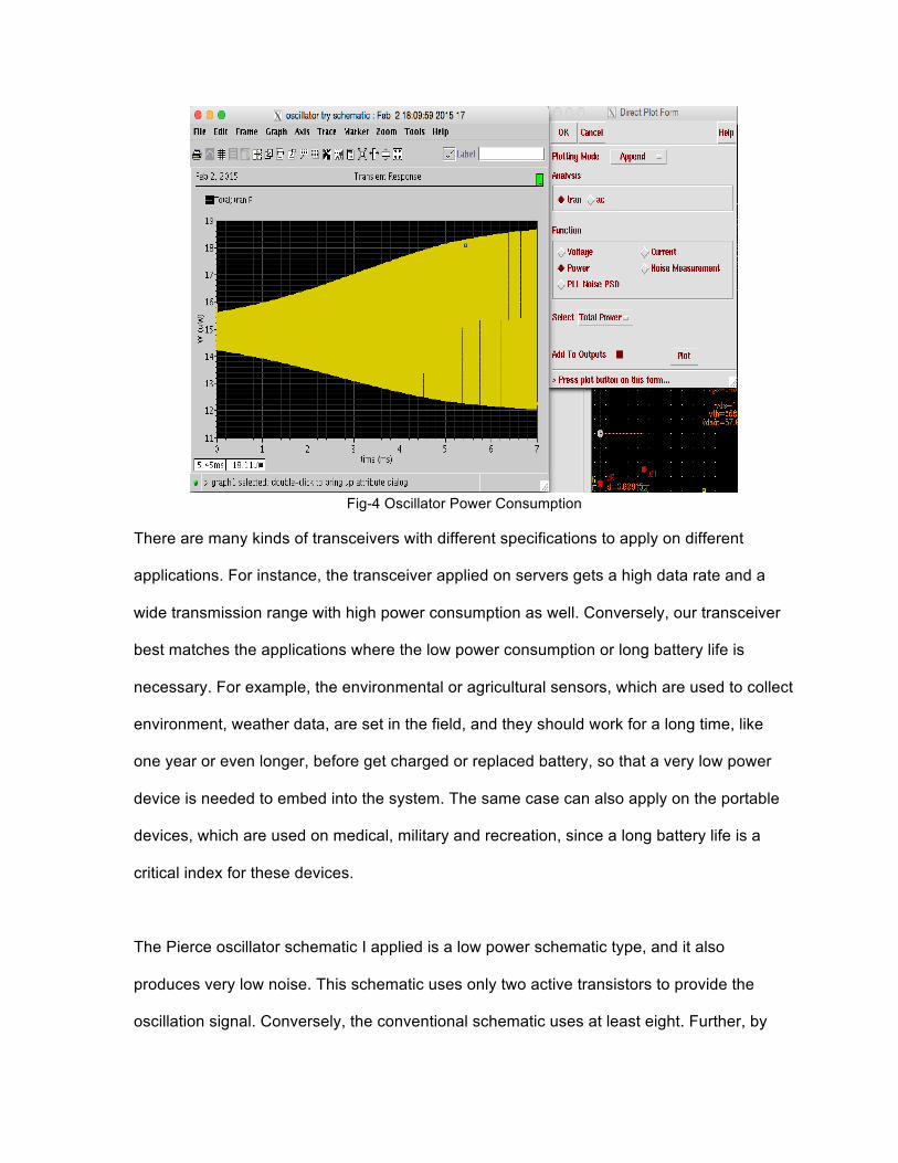
Fig-4 Oscillator Power Consumption
There are many kinds of transceivers with different specifications to apply on different
applications. For instance, the transceiver applied on servers gets a high data rate and a
wide transmission range with high power consumption as well. Conversely, our transceiver
best matches the applications where the low power consumption or long battery life is
necessary. For example, the environmental or agricultural sensors, which are used to collect
environment, weather data, are set in the field, and they should work for a long time, like
one year or even longer, before get charged or replaced battery, so that a very low power
device is needed to embed into the system. The same case can also apply on the portable
devices, which are used on medical, military and recreation, since a long battery life is a
critical index for these devices.
The Pierce oscillator schematic I applied is a low power schematic type, and it also
produces very low noise. This schematic uses only two active transistors to provide the
oscillation signal. Conversely, the conventional schematic uses at least eight. Further, by

adjusting the value of capacitors and resistors in a reasonable range by trading off areas,
the noise generated by the transistors can be reduced. The circuit schematic is shown
below.
Fig-4 Oscillator Schematic
Nowadays, there are several important technologies being used for wireless transmission
technologies, such as Wi-Fi, Zigbee, and Bluetooth, and each of them has their own feature
and applicable areas. For example, Bluetooth is the cheapest technology, with $2.95 per
1000 parts, but the transmission range for Bluetooth is not far enough, which is the reason
why we only Bluetooth to transmit files when two devices are very closed. Wi-Fi is the
fastest transmission technology, the transmission rate can reach 11-54 Mbps/second, so
that it is widely used in public areas for various users and devices, it also has a fine
transmission range, but the problem is its security issue. It is easy for hackers to break into
your Wi-Fi network and get the data. Zigbee has the furthest transmission range, but the
transmission rate is very low, so it is applicable in certain applications but not for everywhere.
As I already mentioned above, our low-power technology gained its own feature, and also
competitive among those popular technologies in certain areas. The major limitation of our

transceiver is where the transmission speed is required, and the power consumption is not
quite important, such as the servers, laptops and cellphones.
• Concluding Reflections
The original goal of my oscillator design was to implement it with the power of 10uW.
However, I finally designed it with the power of 15uW. The reason that I cannot manage to
reach the original goal is that there were parasitic capacitances and resistances, which
consume power in the real design, but I did not take them into calculation. Besides, the
common problem in our group project management is the time management. We were too
optimistic about the progress that we could make, and the main reason is because we
underestimated the workload in our technical courses. In fact, the course work is very heavy
at the late of last term that we barely have enough time to meet the schedule, and
eventually, the plan was postponed to this semester. The experience we gained about
making the timeline is that we need to estimate the actual time that we could spend on this
project more accurately, rather than making a schedule that seems delightful.
There are two major ways to do further research about this topic. Firstly, people could try to
further decrease the power, since it is still fascinating to know what is the real theoretical
limit of MEMS-based transceivers power consumption, so that many applications in the
extreme area can be used. Further, lowing the power consumption could be beneficial to the
energy harvesting technology. When the transceiver is used at some circumstances, where
the energy of the whole system comes from the outside, such as body temperature, solar
energy, instead of using batteries, the power consumption relates to the stability of the
whole system. Therefore, if you could consume less power, then the harvesting energy
demand will decreases, so the low power research gives more relax on other technologies,

so that it produces more possibility to broaden the applicable areas including those extreme
environments.
Secondly, it is always a hot research direction to raise the channel frequency higher and
higher. Actually, a limitation for current MEMS-based transceiver is the frequency limitation
that it can’t work on a very high frequency like Giga-hertz. The transceiver we are currently
using is on 60 Mega-hertz, so the research on high frequency MEMS device will expand the
applicable areas for these kinds of devices.
Of course, this research topic is still valuable for further research. If someone were going to
take over my task, I would recommend him to specifically analyze on the parasitic capacitors
that could exist on the circuits and the system, since these capacitors are the critical limits to
the power consumption of the oscillator. Besides, I would recommend him to simplify the
current source circuit, which is one part of my circuit, and also do more analysis on noise
reduction. Also, there always will be a better design than before, and it is entirely possible
that the power limitation would be further decreased. Thus, people could think about a
completely new design towards the existing one, which consumes less power. For example,
my design includes a current source, which provides current to the common source amplifier.
owever, this current source can also be shared to other blocks, since the existing design of
our group uses duplicate current sources to different blocks, and it should be optimized to
save power for the entire system.

References
[1] Hifiduino (2014). 33.8688MHz Oscillator: Discrete Choice. Retrieved March 14, 2015, from https://hifiduino.wordpress.com/2012/05/26/33-8688-mhz-oscillator-discrete-choice/
[2] T. O. Rocheleau, T. L. Naing, J. N. Nilchi, and C. T.-C. Nguyen, "A MEMS-based tunable RF channel-selecting super-regenerative transceiver for wireless sensor nodes," Tech. Digest, 2014 Hilton Head MEMS Conf., Hilton Head, SC, June 8-12, 2014, pp. 83-86.
IV. Consolidated Paper
This chapter of the report will provide the summary of the system level integration and
performance of the receiver and transmitter. This chapter will provide a summary of the
oscillator, comparator, power amplifier, and buffer blocks.
Oscillator
The function of oscillator in a transceiver system is to create a constant high frequency
signal to carry the information signal. In a transmitter system, the oscillator output modulates the
information signal, and the power amplifier amplifies the signal to be transmitted afterwards. In
the receiver chain, the oscillator and envelope detector demodulates the transmitted signal and
then sends it to comparator for decoding.
The oscillator in this system is designed as a MEMS-based oscillator, where the MEMS
device is used as a resonator to replace the crystal that is used in traditional oscillators. The
advantage of the MEMS-based oscillator is that it provides high Q to have a more accurate
channel selection, and the simple design also contributes to low power consumption.
Oscillators typically consume the majority of power in the receive chain. Therefore, the
topology of the oscillator determines the power consumption of whole system at some degree.
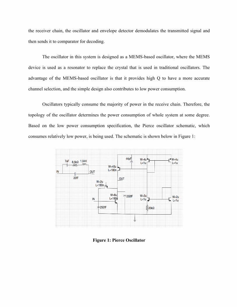
Based on the low power consumption specification, the Pierce oscillator schematic, which
consumes relatively low power, is being used. The schematic is shown below in Figure 1:
Figure 1: Pierce Oscillator

The feedback loop of this oscillator has a phase shift of 360°, and in order to make it
oscillate, we also need to design for a negative resistance greater than 8.5kΩ looking into two
ports of resonator. Since positive resistance consumes power, we can regard negative resistance
as an energy source. If this “energy source” provides energy larger than the power consumption
of resistor in the resonator, then this oscillator can work well.
According to the equation of negative resistance:
In the circuit shown in Figure 1, the nodes “IN” and “OUT” link with the MEMS device
by bond pad connection, and we assume the parasitic capacitance on the bond pad is around
250fF. The transconductance of the common source amplifier is 165.68uA/V, and the value of
negative resistance is 13.66kΩ.
The output waveform and power consumption is shown below in Figure 2 and Figure 3.

Figure 2: Growing Waveform of The Oscillator
Figure 3: Power Consumption of The Oscillator
The resonance frequency of 58.98MHz, and the amplitude is 128mV. The power
consumption is 15uW.
The amplitude of the oscillator output in each period differentiates ‘1’ and ‘0’. The
simulation required different stimulating signals to generate the different growing speed. Further,
the oscillator required a reset to toggle a ‘0’ in simulation. The reset to the oscillator was
generated by switching the resonator resistance to a much higher resistance to destroy the quality
factor. The stimulating circuit with a reset is shown in Figure 4.

Figure 4. Stimulating Circuit
R1 corresponds to the working state, and R2 corresponds to resetting state. When the
circuit switches to R2, the high resistance destroys the quality factor so that the oscillator can no
longer work. The switch S1 is set to be periodically switches between R1 and R2. The output
waveform is shown below in Figure 5.
Figure 5. Output Waveform of Oscillator
In addition, an FSK signal is needed on the transmitter side. The method to generate an
FSK signal is to switch the value of capacitance between two values. 7aF capacitance was used

to generate 59MHz signal, and 6.5aF capacitance to generate 61MHz signal. The MEMS
resonator model is shown below in Figure 6:
Figure 6. MEMS Resonator Model
Design Specification Value
Resonance frequency 58.9MHz
Power Consumption 15uW
Envelope Detector
The envelope detector designed is a key piece of the transceiver system because it serves
to detect the information stored in the envelope of wireless signals. In order to bias the envelope
detector circuit into a temperature stable state of operation, a temperature independent current
source was implemented. This temperature independent current source was also taken advantage
of by the oscillator and the buffer circuits.
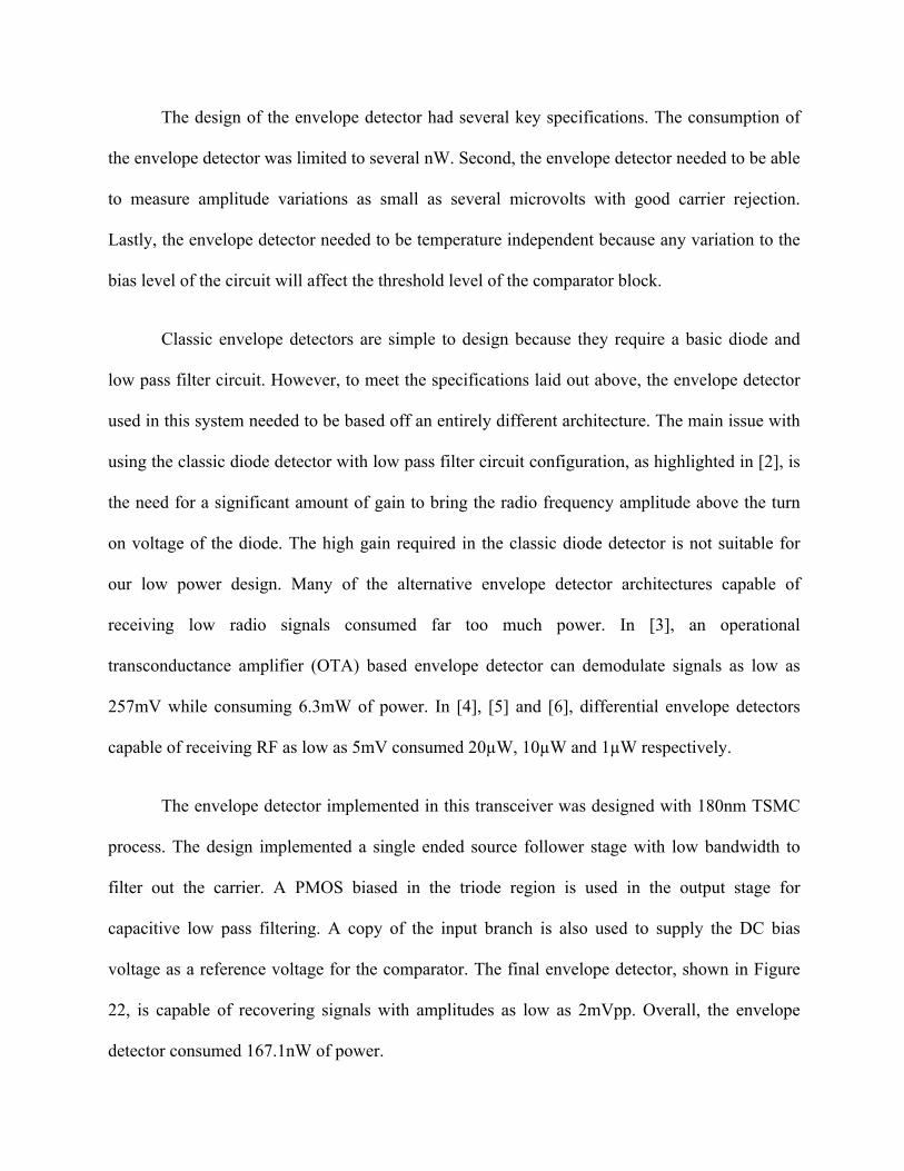
The design of the envelope detector had several key specifications. The consumption of
the envelope detector was limited to several nW. Second, the envelope detector needed to be able
to measure amplitude variations as small as several microvolts with good carrier rejection.
Lastly, the envelope detector needed to be temperature independent because any variation to the
bias level of the circuit will affect the threshold level of the comparator block.
Classic envelope detectors are simple to design because they require a basic diode and
low pass filter circuit. However, to meet the specifications laid out above, the envelope detector
used in this system needed to be based off an entirely different architecture. The main issue with
using the classic diode detector with low pass filter circuit configuration, as highlighted in [2], is
the need for a significant amount of gain to bring the radio frequency amplitude above the turn
on voltage of the diode. The high gain required in the classic diode detector is not suitable for
our low power design. Many of the alternative envelope detector architectures capable of
receiving low radio signals consumed far too much power. In [3], an operational
transconductance amplifier (OTA) based envelope detector can demodulate signals as low as
257mV while consuming 6.3mW of power. In [4], [5] and [6], differential envelope detectors
capable of receiving RF as low as 5mV consumed 20µW, 10µW and 1µW respectively.
The envelope detector implemented in this transceiver was designed with 180nm TSMC
process. The design implemented a single ended source follower stage with low bandwidth to
filter out the carrier. A PMOS biased in the triode region is used in the output stage for
capacitive low pass filtering. A copy of the input branch is also used to supply the DC bias
voltage as a reference voltage for the comparator. The final envelope detector, shown in Figure
22, is capable of recovering signals with amplitudes as low as 2mVpp. Overall, the envelope
detector consumed 167.1nW of power.
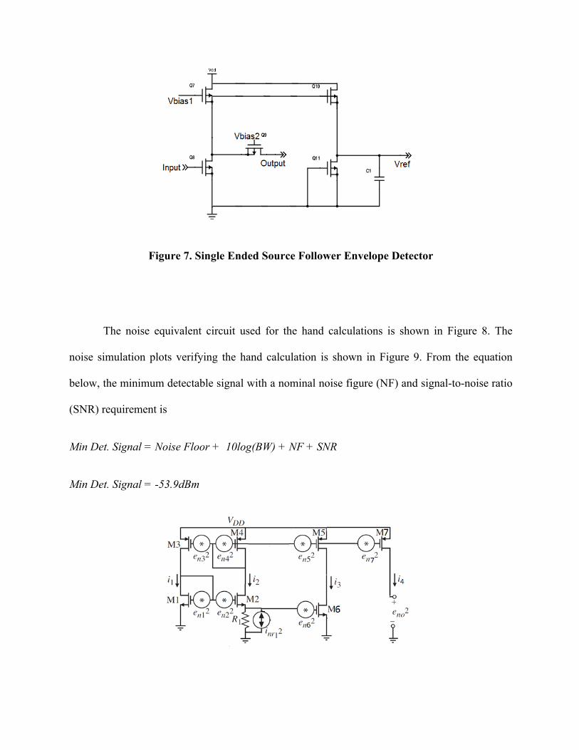
Figure 7. Single Ended Source Follower Envelope Detector
The noise equivalent circuit used for the hand calculations is shown in Figure 8. The
noise simulation plots verifying the hand calculation is shown in Figure 9. From the equation
below, the minimum detectable signal with a nominal noise figure (NF) and signal-to-noise ratio
(SNR) requirement is
Min Det. Signal = Noise Floor + 10log(BW) + NF + SNR
Min Det. Signal = -53.9dBm

Figure 8. Noise Equivalent Circuit
Figure 9. Noise Plot
Therefore, the minimum detectable is 2mVpp. The simulation proving the ability to
demodulate signals with 2mVpp amplitude is shown in Figure 10. On the other end of the
spectrum, the maximum amplitude the envelope detector can detect before clipping is simulated
to be 1V. Therefore, the dynamic range of this block is
0dBm-(-53.9dBM) =53.9dB.

Figure 10. Minimum Detectable Signal
The envelope detector discussed was biased with 83nA of current and required stable
reference supply. The design of the reference followed the methodology proposed in [7], which
discusses a stable bandgap reference. The final design of the current reference is shown in Figure
11 and is capable of supplying 83nA of current with a 0.3% variation across the 0°C to 70°C
temperature range. This stability was achieved by cancelling the temperature dependence of the
resistor in the circuit with a diode connected NMOS transistor in parallel. The low current supply
was achieved using maximum long channel devices in 180nm TSMC transistors.

Figure 11. Temperature Independent Current Reference
The final design of the envelope detector with current reference is shown in Figure 12.
Figure 12. Envelope Detector and Current Reference

As part of the integration process, the layout of the envelope detector, current reference
and the oscillator was designed. The layout is shown in Figure 7 with a die area of 750um^2.
Figure 13. Layout of Oscillator, Current Supply, and Envelope Detector
Block Summary
Envelope Detector
Minimum Detectable Signal 2mVpp
Dynamic Range 53.9dB
Envelope Delay .5us

Envelope Bandwidth 1MHz
Carrier Bandwidth 500MHz
Total Power Consumption 167.1nW
Current Reference
DC Current 0°C 83.21nA
DC Current 25°C 83.55nA
DC Current 70°C 83.89nA
Total Power Consumption 250.6nW
Layout
Die Size (Oscillator, Envelope Detector, Current Source) 750um^2
Comparator
When Frequency Shift Keying (FSK) modulated signals enter the transceiver, they give
rise to the periodically restarted oscillations [1]. When the oscillation envelope is detected, the
comparator should be able to discriminate “0”s and “1”s [1].
The schematic for the comparator is shown below in Figure 14.
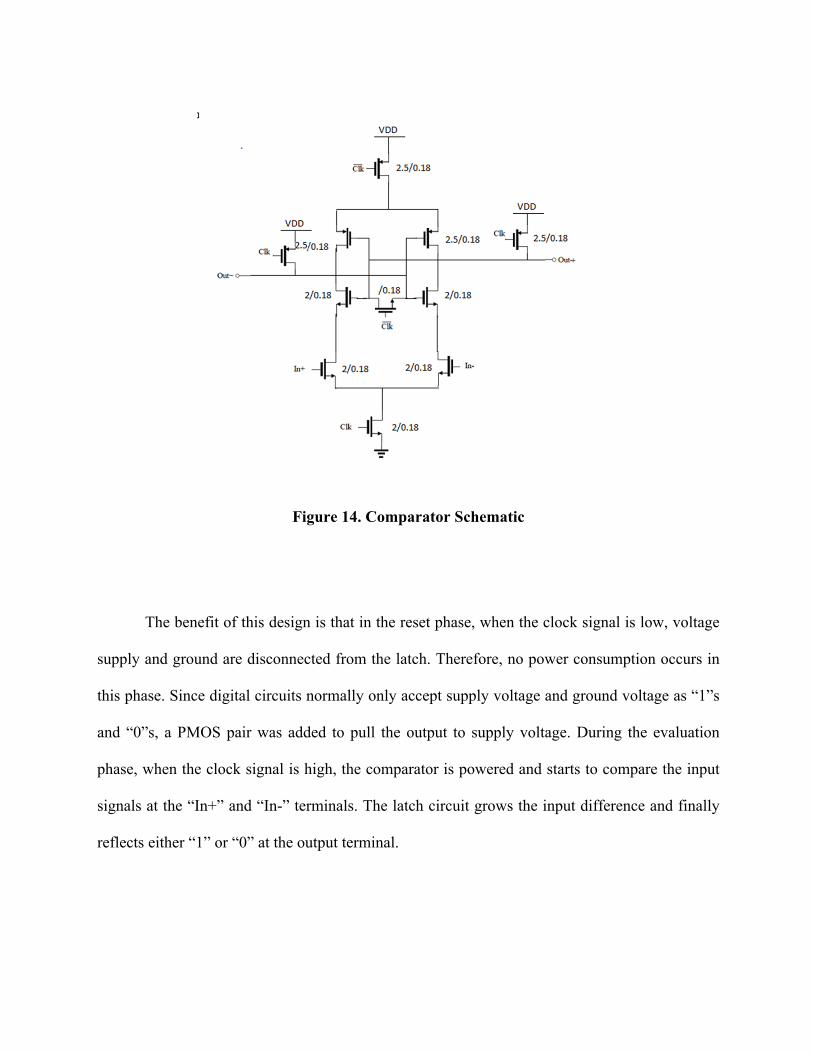
Figure 14. Comparator Schematic
The benefit of this design is that in the reset phase, when the clock signal is low, voltage
supply and ground are disconnected from the latch. Therefore, no power consumption occurs in
this phase. Since digital circuits normally only accept supply voltage and ground voltage as “1”s
and “0”s, a PMOS pair was added to pull the output to supply voltage. During the evaluation
phase, when the clock signal is high, the comparator is powered and starts to compare the input
signals at the “In+” and “In-” terminals. The latch circuit grows the input difference and finally
reflects either “1” or “0” at the output terminal.
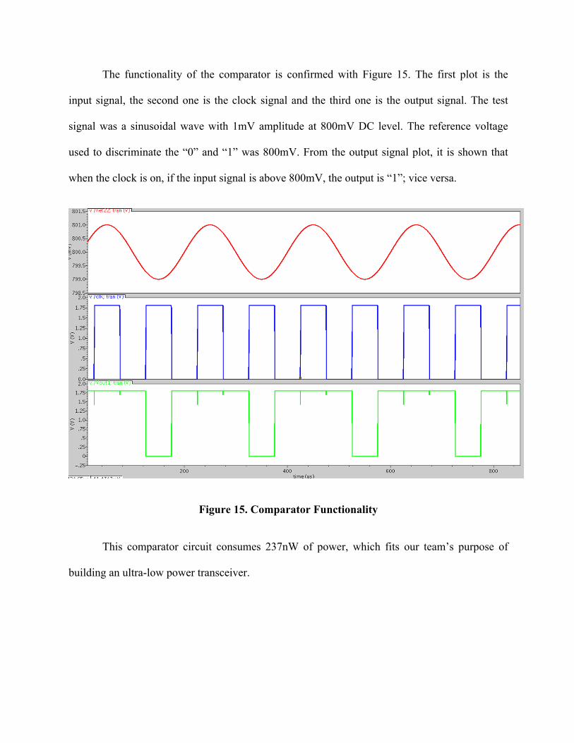
The functionality of the comparator is confirmed with Figure 15. The first plot is the
input signal, the second one is the clock signal and the third one is the output signal. The test
signal was a sinusoidal wave with 1mV amplitude at 800mV DC level. The reference voltage
used to discriminate the “0” and “1” was 800mV. From the output signal plot, it is shown that
when the clock is on, if the input signal is above 800mV, the output is “1”; vice versa.
Figure 15. Comparator Functionality
This comparator circuit consumes 237nW of power, which fits our team’s purpose of
building an ultra-low power transceiver.
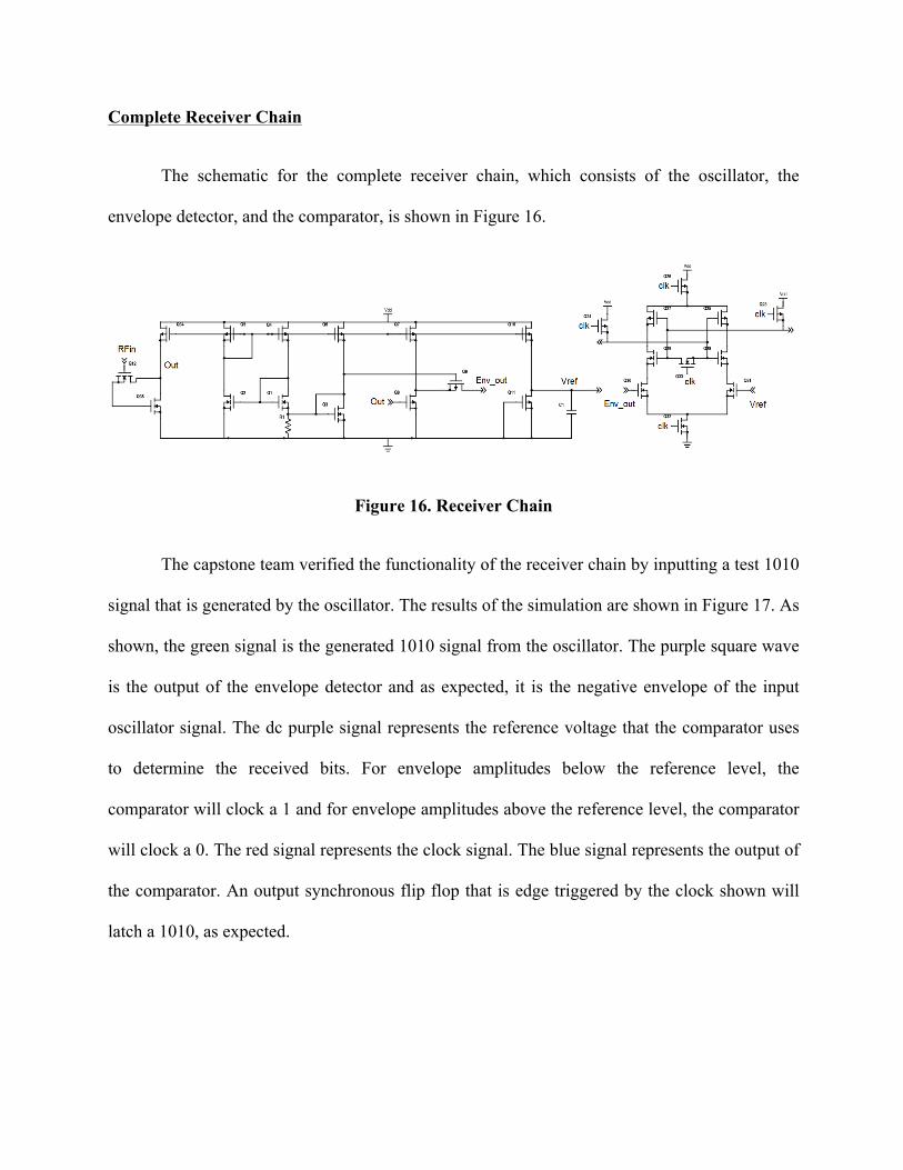
Complete Receiver Chain
The schematic for the complete receiver chain, which consists of the oscillator, the
envelope detector, and the comparator, is shown in Figure 16.
Figure 16. Receiver Chain
The capstone team verified the functionality of the receiver chain by inputting a test 1010
signal that is generated by the oscillator. The results of the simulation are shown in Figure 17. As
shown, the green signal is the generated 1010 signal from the oscillator. The purple square wave
is the output of the envelope detector and as expected, it is the negative envelope of the input
oscillator signal. The dc purple signal represents the reference voltage that the comparator uses
to determine the received bits. For envelope amplitudes below the reference level, the
comparator will clock a 1 and for envelope amplitudes above the reference level, the comparator
will clock a 0. The red signal represents the clock signal. The blue signal represents the output of
the comparator. An output synchronous flip flop that is edge triggered by the clock shown will
latch a 1010, as expected.
Figure 17. Verification of Receiver
Power Amplifier
This part of the paper summarizes the design of a Power amplifier (PA) for the
transmitter part of the system. This block functions to establish connections and send information
from the digital system to the external world.
Given the fact that reducing the power consumption is the overall goal of this project, the
power consumed by the individual blocks must also be minimized. This translates to the concept
of power efficiency, meaning ‘the amount of power used to generate and transmit a decodable
burst of data from the system’. The major trade off for efficiency is a characteristic called
linearity. Linearity defines ‘the relationship between the output and the input, and the change in

output for a given change in the input level’. Below is a table of the performance statistics of
each of the power amplifier classes available.
CLASS A B C D E
Theoretical efficiency 50% 78.5% 80% 100% 100%
Linearity Linear Non-linear Non-linear Non-linear Non-linear
Since efficiency is our major consideration in this system, a class D amplifier was used.
This choice was made after surveying highly efficient PA’s in papers written in [8] and [9]. The
other requirements needed for proper operation of the PA block include current bias generation,
voltage bias at the input, and inclusion of passives.
Figure 18. Class D & E Amplifier models [10]
From the above table, class D and class E amplifiers can be theoretically characterized as
having an efficiency of 100% [10], this is because they don’t allow for any dissipation of energy

within the system, thus translating all of its energy to the required output load, which is an
antenna used for transmission in most cases.
Figure 19. Architecture of the Power Amplifier
The control over power transmitted to the load depends on the impedance (resistance) of
the load seen by the output node of the amplifier. In order to meet the specification of the power
drawn by the load precisely, this load seen by the output node has to be transformed to a
different value. This process of transforming the load can be done by using a network called
‘matching network’ to match the output node to the impedance needed for maximum power
transfer. For this power amplifier, a T-match was employed because it isolates the DC
component and the AC component – which is of our interest at the output node and also provides
the impedance transformation needed. The final schematic of the power amplifier is shown in
Figure 20.
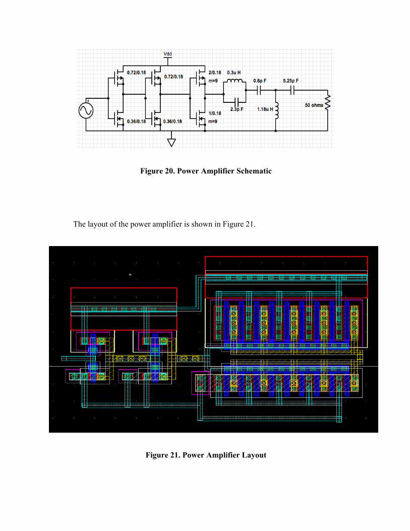
Figure 20. Power Amplifier Schematic
The layout of the power amplifier is shown in Figure 21.
Figure 21. Power Amplifier Layout

Following waveforms show the simulated results for the various performance metrics.
POWER-GAIN & OUTPUT WAVEFORMS: The reported power gain is 47 dB at the
fundamental frequency. Waveforms below depict the voltage and current waveforms at the port
or the virtual antenna. We can see that the waveforms are purely sinusoidal.
Figure 22: measured power gain & simulated output waveforms
POWER: The first plot shows the power levels without the L–match filtering at the port. The
second plot shows the power levels with both the L-match filtering at the port and 3rd harmonic
filtering. We see that harmonic power is high and can affect the efficiency.
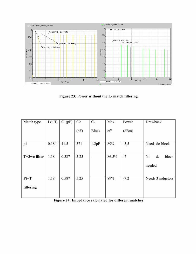
Figure 23: Power without the L- match filtering
Match type L(uH) C1(pF) C2
(pF)
C-
Block
Max
eff
Power
(dBm)
Drawback
pi 0.184 41.5 371 1.2pF 89% -3.5 Needs dc-block
T+3wo filter 1.18 0.587 5.25 - 86.5% -7 No dc block
needed
Pi+T
filtering
1.18 0.587 5.25 89% -7.2 Needs 3 inductors
Figure 24: Impedance calculated for different matches

EFFICIENCY: The reported efficiency is 88.35%.
Figure 25: Measured efficiency with filtering & before harmonic “block network”
It is evident that the efficiency improves by 16%, by adding a third harmonic block.
DRAIN WAVEFORMS:
Figure 26: Drain waveforms Ideal class D output waveforms
The contributors for efficiency degradation are:
1. Harmonic dissipation: we see that the total harmonic power added from the second to 19th
harmonic sums up to 1.2% after adding the 3rd harmonic filter.
2. Parasitic losses: The passive devices have a quality factor of 20.Therefore, the internal
resistance of the components adds up to a loss of 2.4%.
3. C*V^2*f Losses: The input gate capacitance of the inverters is 1.5f F each and the
amplification stage offers a gate cap of 31f F. This produces a loss of 6.722uW = 3.4 %
Short circuit current Harmonics Passive parasitics Driver C*V^2*f Total loss
loss 6.4% 1.2% 2.4% 3.4% 13.4%
Figure 27: Loss contributors
Transmit Chain
The oscillator is integrated with the Power amplifier by connecting the output of the
oscillator to the input of the PA. An input FSK is generated by the oscillator and given to the PA.
The plot below in Figure 28 shows how an input data stream is modulated and
transmitted by the power amplifier into the antenna.

Figure 28. Transmit Waveform
Voltage Buffer
We require a voltage buffer to interface with the 50Ω transmission line required to test
our chip. This voltage buffer has several design requirements. The most important is a voltage
gain of 1 to accurately represent the input signal. Impedance matching at the output is necessary
to ensure that the maximum available power from the input signal is delivered to the load. The
buffer also requires high enough bandwidth, output voltage swing, and linearity to send signals
to the output negligible distortion. The input signals of interest are the output signals of each
block in the transceiver chain except the power amplifier; in general, these are a 60Mhz signal
with 0.8V peak to peak (pk-pk) and a 5khz signal with 1.8Vpk-pk. A bandwidth requirement of
600Mhz is necessary to capture harmonics of the 60Mhz signal. Die area and power
consumption will not be considered as primary design constraints. Since our project is currently
focused on verifying functionality, cost and commercialization details are not concerns.

Additionally, the buffer will connect a separate power rail from the rest of the transceiver to
negate its power contribution during normal operation of the MEMS transceiver.
Given the design requirements presented, two different buffer topologies were
implemented. A wideband buffer was designed for 60MHz while a rail-to-rail buffer was
designed for 5 kHz. For the purposes of this paper, which is to discuss the integration of the
voltage buffer into the transceiver system, we encourage the reader to briefly refer to the
summary of the performance of both buffers as given in the “Individual Technical
Contributions” report for the voltage buffer. Details on the topologies, transistor sizes, design
methodology, and test results of the buffers is discussed in more detail in that report.
The integration of the voltage buffer to the transceiver system required proper modeling
of the interface between the buffer and the block being measured. The additional capacitance that
would be added after attaching the buffer must be taken into consideration during design time for
the measured block. The input PMOS device of the wideband buffers were sized to be
20um/180nm, which resulted in an input loading of ~10fF. Since the functionality of both the
envelope detector and the oscillator already required large capacitances on the order of ~100fF at
their outputs, this additional loading was not a concern. The integration of the comparator with
the rail-to-rail buffer was more challenging; the input of this buffer had a PMOS device with size
36u/180nm in parallel with a NMOS device with size 12u/180nm, which summed to a significant
capacitance. A redesign of the transistor sizes in the comparator was necessary. Figure 29 shows
the schematic and resulting plots of a rail-to-rail buffer integrated with the redesigned
comparator. As shown in part (b) of the figure, the output of the buffer follows the comparator’s
output up to its maximum voltage swing of 1.67V, which is the expected performance.
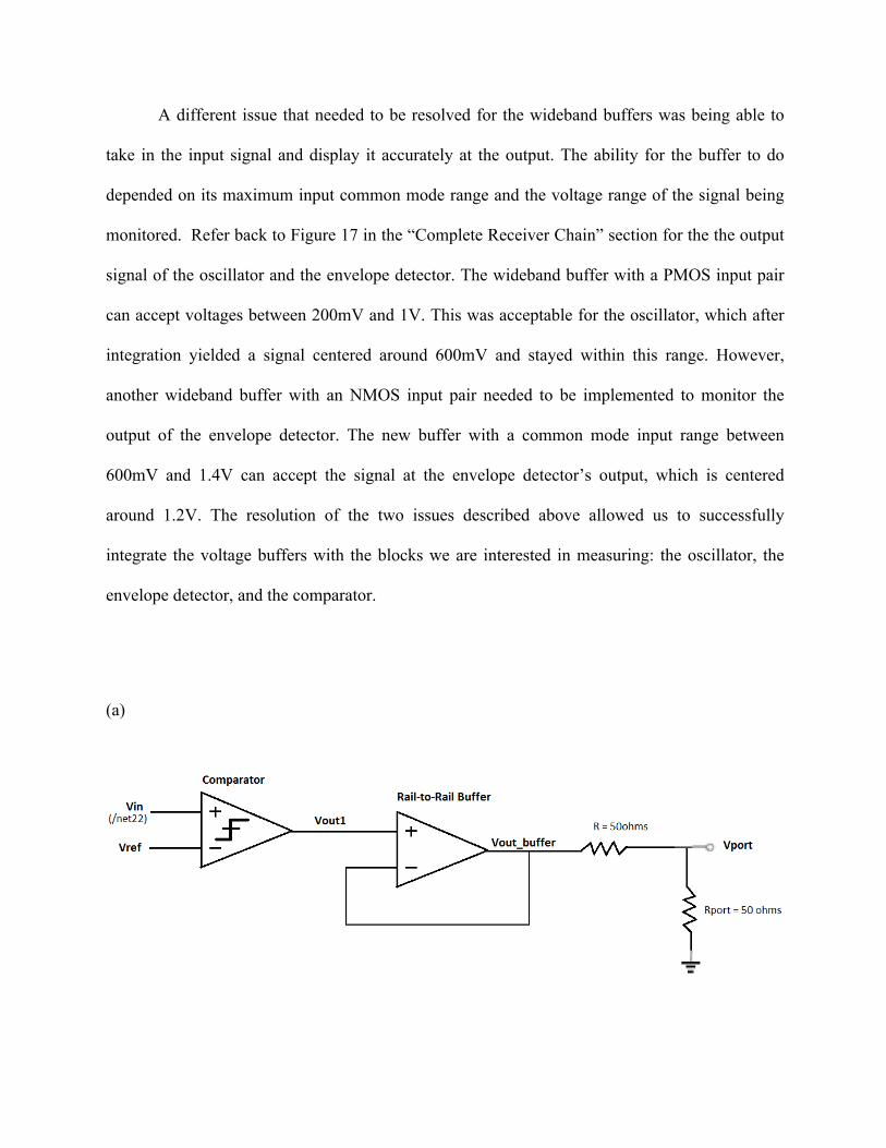
A different issue that needed to be resolved for the wideband buffers was being able to
take in the input signal and display it accurately at the output. The ability for the buffer to do
depended on its maximum input common mode range and the voltage range of the signal being
monitored. Refer back to Figure 17 in the “Complete Receiver Chain” section for the the output
signal of the oscillator and the envelope detector. The wideband buffer with a PMOS input pair
can accept voltages between 200mV and 1V. This was acceptable for the oscillator, which after
integration yielded a signal centered around 600mV and stayed within this range. However,
another wideband buffer with an NMOS input pair needed to be implemented to monitor the
output of the envelope detector. The new buffer with a common mode input range between
600mV and 1.4V can accept the signal at the envelope detector’s output, which is centered
around 1.2V. The resolution of the two issues described above allowed us to successfully
integrate the voltage buffers with the blocks we are interested in measuring: the oscillator, the
envelope detector, and the comparator.
(a)

(b)
Figure 29: Test Setup (part a) and Transient Response (part b) for comparator and rail-to-
rail buffer. Blue trace is the test signal (output of envelope detector), purple trace shows
output of the comparator, green trace shows the output of the voltage buffer, and red
signal shows the signal being sent to the load after matching.

Work Cited
[1] Rocheleau, Tristan. "“A MEMS-based Tunable RF Channel-selecting Super-regenerative Transceiver for Wireless Sensor Nodes." Solid-State Sensors, Actuators and Microsystems Workshop (2014): n. pag. Web.
[2] Gambini, Simone. "Sensitivity Analysis for AM Detectors." Sensitivity Analysis for AM Detectors. UC Berkeley, 6 Apr. 2008. Web. 10 Mar. 2015. <http://www.eecs.berkeley.edu/Pubs/TechRpts/2008/EECS-2008-31.html>.
[3] Zhou, Yanping. "A Novel Wide-band Envelope Detector." IEEE Xplore. N.p., 17 June 2008. Web. 10 Mar. 2015. <http://ieeexplore.ieee.org/xpl/articleDetails.jsp?arnumber=4561422>.
[4] R.G. Meyer Low-power monolithic RF peak detector analysis IEEE Journal of Solid-State Circuits, January 1995.
[5] D.C.Daly and A.Chandrakasan An energy efficient OOK transceiver for wireless sensor networks IEEE Journal of Solid-state Circuits, May 2007.
[6] Pletcher, Nathan, Jan Rabaey, and Simone Gambini. "A 65uW, 1.9 GHz RF to Digital
Baseband Wakeup Receiver for Wireless Sensor Nodes." IEEE Xplore. N.p., 16 Sept. 2007. Web. 10 Mar. 2015. <http://ieeexplore.ieee.org/xpls/abs_all.jsp?arnumber=4405789>.
[7] Alon, Elad. "EE240: Advanced Analog Integrated Circuits Lectures." EE240 (Spring 2009). N.p., 2009. Web. 10 Mar. 2015. <http://bwrcs.eecs.berkeley.edu/Classes/icdesign/ee240_sp10/lectures.html>.
[8] Nathan o. sokal,(1981) ieee life fellow design automation, inc: Class-e high-efficiency rf/microwave power amplifiers: principles of operation, design procedures, and experimental verification retrieved Feburary 1981 from: http://www.cs.berkeley.edu/~culler/AIIT/papers/radio/Sokal%20AACD5-poweramps.pdf
[9] N.O.Sokal and A.D.Sokal (1975),“Class E—A new class of high-efficiency tuned single-ended switching power amplifiers,” IEEE J. Solid-State Circuits, vol. SC-10, no. 6, pp. 168–176, Jun. 1975. http://ieeexplore.ieee.org/xpls/abs_all.jsp?arnumber=1050582
[10] Ali.M.Niknejad (2014): RFIC ,UC Berkeley; EE242B, retrieved fall 2014 from: http://rfic.eecs.berkeley.edu/ee242/lectures.html

V. Concluding Reflections
The main technical knowledge that I acquire from this capstone project is the transceiver
design, especially the oscillator design. It is a good introduction for me to get familiar with those
transceiver blocks and have some basic knowledge about it. By participating meetings with
Professor Nguyen, Tristan and Thura, I gradually understand how people do research. It is
different from taking classes and doing course projects, which usually have clear instruction to
follow. But doing research needs people to explore everything by yourself. This difference
makes us quite uncomfortable at the beginning of the project, since we do not have a transceiver
design background, but we are always told to find out the answers by ourselves.
Through this project, I also learn some project management skills. We set up a pretty ambitious
plan at the beginning, which is to finish the schematic and layout by the end of December, and
send it to layout. But the reality is that we didn’t even finish the schematic. The problem here is
that we didn’t estimate the working load, the working hours on this project correctly. Therefore,
when we made the plan this semester again, we made a more realistic plan and manage to finish
it.
Since each person is assigned to do one different block separately, we didn’t collaborate much
except for the last part of the project. It is better if we could collaborate for some parts and also
individually do some work at the same time.
Related Documents