1 SWCU174A – July 2014 – Revised March 2017 Submit Documentation Feedback Copyright © 2014–2017, Texas Instruments Incorporated TPS65903x-Q1 EVM User’s Guide User's Guide SWCU174A – July 2014 – Revised March 2017 TPS65903x-Q1 EVM User’s Guide This user’s guide describes the characteristics, operation, and use of the TPS65903x-Q1 EVM. An EVM description, GUI description, interface requirements, and complete schematic are included. Contents 1 Introduction ................................................................................................................... 1 1.1 EVM Overview ...................................................................................................... 2 1.2 EVM with Components Identified ................................................................................. 2 1.3 Power-Supply Requirements and Connections ................................................................. 3 1.4 Default Jumper Settings ........................................................................................... 4 2 EVM Schematics............................................................................................................. 7 3 EVM BOM .................................................................................................................... 9 4 Powering up the Device ................................................................................................... 11 5 TPS65903x-Q1EVM Graphical User Interface (GUI) .................................................................. 12 5.1 GUI Tabs ........................................................................................................... 12 5.2 Running a Script with the GUI ................................................................................... 14 List of Figures 1 EVM ........................................................................................................................... 2 2 Power Supply ................................................................................................................ 3 3 EVM Schematic .............................................................................................................. 7 4 EVM Schematic .............................................................................................................. 8 5 DUT_Control ................................................................................................................ 12 6 Registers .................................................................................................................... 13 7 Sample Script ............................................................................................................... 14 List of Tables 1 Default Jumper Settings for the TPS659038EVM ....................................................................... 4 2 EVM BOM .................................................................................................................... 9 Trademarks MSP430 is a trademark of Texas Instruments. Windows is a registered trademark of Microsoft Corporation. All other trademarks are the property of their respective owners. 1 Introduction The TPS659038-Q1 and TPS659039-Q1 devices are power-management integrated circuits (PMICs) for automotive applications. The device provides seven configurable step-down converters, with up to 9 A of output current for memory, processor core, input/output (I/O), or preregulation of LDOs. The TPS659038- Q1 device contains 11 LDO regulators while the TPS659039-Q1 device contains 6 LDO regulators for external use. For more details, see the device data sheet, TPS65903x-Q1 Automotive Power Management Unit (PMU) for Processor.

Welcome message from author
This document is posted to help you gain knowledge. Please leave a comment to let me know what you think about it! Share it to your friends and learn new things together.
Transcript
1SWCU174A–July 2014–Revised March 2017Submit Documentation Feedback
Copyright © 2014–2017, Texas Instruments Incorporated
TPS65903x-Q1 EVM User’s Guide
User's GuideSWCU174A–July 2014–Revised March 2017
TPS65903x-Q1 EVM User’s Guide
This user’s guide describes the characteristics, operation, and use of the TPS65903x-Q1 EVM. An EVMdescription, GUI description, interface requirements, and complete schematic are included.
Contents1 Introduction ................................................................................................................... 1
1.1 EVM Overview ...................................................................................................... 21.2 EVM with Components Identified ................................................................................. 21.3 Power-Supply Requirements and Connections................................................................. 31.4 Default Jumper Settings ........................................................................................... 4
2 EVM Schematics............................................................................................................. 73 EVM BOM .................................................................................................................... 94 Powering up the Device ................................................................................................... 115 TPS65903x-Q1EVM Graphical User Interface (GUI).................................................................. 12
5.1 GUI Tabs ........................................................................................................... 125.2 Running a Script with the GUI ................................................................................... 14
List of Figures
1 EVM ........................................................................................................................... 22 Power Supply ................................................................................................................ 33 EVM Schematic .............................................................................................................. 74 EVM Schematic .............................................................................................................. 85 DUT_Control ................................................................................................................ 126 Registers .................................................................................................................... 137 Sample Script ............................................................................................................... 14
List of Tables
1 Default Jumper Settings for the TPS659038EVM ....................................................................... 42 EVM BOM .................................................................................................................... 9
TrademarksMSP430 is a trademark of Texas Instruments.Windows is a registered trademark of Microsoft Corporation.All other trademarks are the property of their respective owners.
1 IntroductionThe TPS659038-Q1 and TPS659039-Q1 devices are power-management integrated circuits (PMICs) forautomotive applications. The device provides seven configurable step-down converters, with up to 9 A ofoutput current for memory, processor core, input/output (I/O), or preregulation of LDOs. The TPS659038-Q1 device contains 11 LDO regulators while the TPS659039-Q1 device contains 6 LDO regulators forexternal use. For more details, see the device data sheet, TPS65903x-Q1 Automotive PowerManagement Unit (PMU) for Processor.
USB
SMPS7
MSP430
SMPS45
LEDs:
POWERGOOD
RESET_OUT
LDORTC
MSP430
SMPS6 SMPS9 SMPS8VIO Selection
(J31)
LDO Outputs (J46)
GPIOs (J27)
SMPS12/3
SMPS3
VSYS (J20)
3.135 V to 5.25 V
GND
Introduction www.ti.com
2 SWCU174A–July 2014–Revised March 2017Submit Documentation Feedback
Copyright © 2014–2017, Texas Instruments Incorporated
TPS65903x-Q1 EVM User’s Guide
1.1 EVM OverviewThe features of this EVM are as follows:• Allows monitoring of all LDO and SMPS output voltages.• Allows loading of all SMPS outputs.• Allows access to the GPIOs and other logic signals to test functionality.• Optimized layout for stable operation of all SMPS.• Onboard MSP430™ microcontroller to enable communication with the PMIC.• Graphical User Interface (GUI) on Windows® to allow access to the registers of the PMIC through
USB-I2C.
1.2 EVM with Components Identified
Figure 1. EVM
LEDs —Display status of POWERGOOD, RESET_OUT, LDORTC and power supply of MSP430
USB —Connection to PC to enable communication through the GUI
MSP430 —Microcontroller used to convert USB data to I2C format
SMPSxx —Monitor point for SMPS outputs
J46 —Monitor point for LDO outputs
J31 —Jumper used to select VIO voltage. J31 requires a jumper installed (only one), and by default is inposition 10, 1V8.
J27 —Jumper that provides access to the GPIOs
J20 —VSYS power supply input. J20 is the same connector as SMPS123, and must not be confused toprevent applying VSYS to SMSP123-output.
www.ti.com Introduction
3SWCU174A–July 2014–Revised March 2017Submit Documentation Feedback
Copyright © 2014–2017, Texas Instruments Incorporated
TPS65903x-Q1 EVM User’s Guide
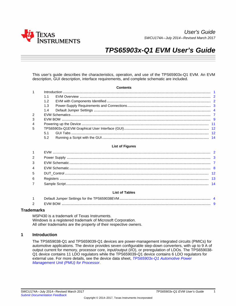
1.3 Power-Supply Requirements and ConnectionsOnly one power supply is needed to power the VSYS domain of the PMIC. Apply 3.135 VDC to 5.25 VDCto the J20 connector of the TPS659038EVM to supply power to the PMIC device. Four-wire sensing of theinput power supply is recommended and can be achieved through the middle two terminals of J20.
Power for the MSP430 and the two fixed voltage LDOs (3.3-V and 1.8-V outputs) is supplied through theUSB connection, as shown in Figure 2.
Figure 2. Power Supply
Introduction www.ti.com
4 SWCU174A–July 2014–Revised March 2017Submit Documentation Feedback
Copyright © 2014–2017, Texas Instruments Incorporated
TPS65903x-Q1 EVM User’s Guide
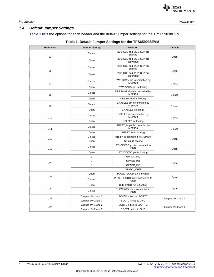
1.4 Default Jumper SettingsTable 1 lists the options for each header and the default jumper settings for the TPS659038EVM.
Table 1. Default Jumper Settings for the TPS659038EVMReference Jumper Setting Function Default
J3Closed I2C1_SCL and I2C1_SDA are
shortedOpen
Open I2C1_SCL and I2C1_SDA areseparated
J5Closed I2C2_SCL and I2C2_SDA are
shortedOpen
Open I2C2_SCL and I2C2_SDA areseparated
J7Closed PWRDOWN pin is controlled by
MSP430 ClosedOpen PWRDOWN pin is floating
J8Closed NRESWARM pin is controlled by
MSP430 ClosedOpen NRESWARM is floating
J9Closed ENABLE1 pin is controlled by
MSP430 ClosedOpen ENABLE1 is floating
J10Closed NSLEEP pin is controlled by
MSP430 ClosedOpen NSLEEP is floating
J11Closed RESET_IN pin is controlled by
MSP430 ClosedOpen RESET_IN is floating
J12Closed INT pin is connected to MSP430
OpenOpen INT pin is floating
J13Closed SYNCDCDC pin is connected to
GND OpenOpen SYNCDCDC pin is floating
J22
1 GPADC_IN0
Open2 GPADC_IN1
3 GPADC_IN2
4 GPADC_VREF
J23Open POWERGOOD pin is floating
OpenClosed POWERGOOD pin is connected to
GND
J24Open CLK32KGO pin is floating
OpenClosed CLK32KGO pin is connected to
GND
J25Jumper b/w 1 and 2 BOOT0 is tied to LDORTC
Jumper b/w 2 and 3Jumper b/w 2 and 3 BOOT0 is tied to GND
J26Jumper b/w 1 and 2 BOOT1 is tied to LDORTC
Jumper b/w 2 and 3Jumper b/w 2 and 3 BOOT1 is tied to GND
www.ti.com Introduction
5SWCU174A–July 2014–Revised March 2017Submit Documentation Feedback
Copyright © 2014–2017, Texas Instruments Incorporated
TPS65903x-Q1 EVM User’s Guide
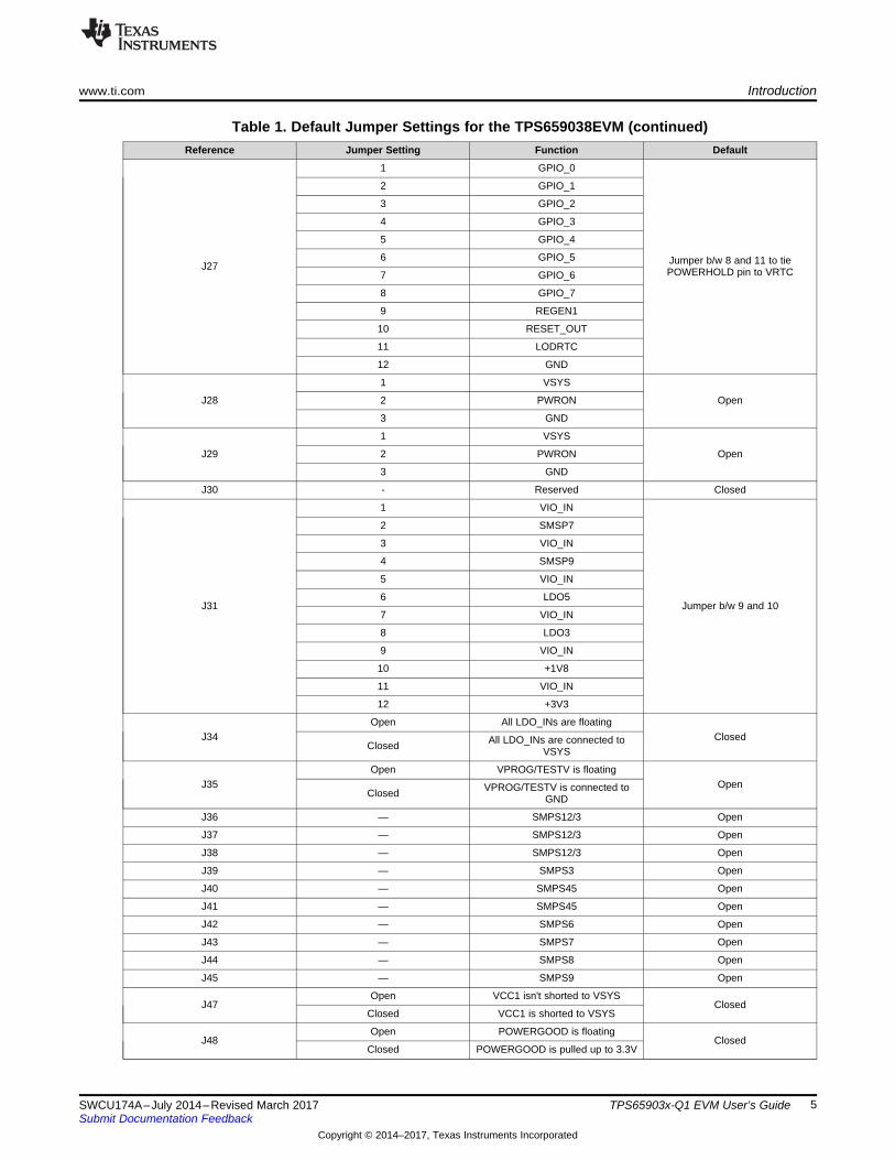
Table 1. Default Jumper Settings for the TPS659038EVM (continued)Reference Jumper Setting Function Default
J27
1 GPIO_0
Jumper b/w 8 and 11 to tiePOWERHOLD pin to VRTC
2 GPIO_1
3 GPIO_2
4 GPIO_3
5 GPIO_4
6 GPIO_5
7 GPIO_6
8 GPIO_7
9 REGEN1
10 RESET_OUT
11 LODRTC
12 GND
J28
1 VSYS
Open2 PWRON
3 GND
J29
1 VSYS
Open2 PWRON
3 GND
J30 - Reserved Closed
J31
1 VIO_IN
Jumper b/w 9 and 10
2 SMSP7
3 VIO_IN
4 SMSP9
5 VIO_IN
6 LDO5
7 VIO_IN
8 LDO3
9 VIO_IN
10 +1V8
11 VIO_IN
12 +3V3
J34Open All LDO_INs are floating
ClosedClosed All LDO_INs are connected to
VSYS
J35Open VPROG/TESTV is floating
OpenClosed VPROG/TESTV is connected to
GND
J36 — SMPS12/3 Open
J37 — SMPS12/3 Open
J38 — SMPS12/3 Open
J39 — SMPS3 Open
J40 — SMPS45 Open
J41 — SMPS45 Open
J42 — SMPS6 Open
J43 — SMPS7 Open
J44 — SMPS8 Open
J45 — SMPS9 Open
J47Open VCC1 isn't shorted to VSYS
ClosedClosed VCC1 is shorted to VSYS
J48Open POWERGOOD is floating
ClosedClosed POWERGOOD is pulled up to 3.3V
Introduction www.ti.com
6 SWCU174A–July 2014–Revised March 2017Submit Documentation Feedback
Copyright © 2014–2017, Texas Instruments Incorporated
TPS65903x-Q1 EVM User’s Guide
Table 1. Default Jumper Settings for the TPS659038EVM (continued)Reference Jumper Setting Function Default
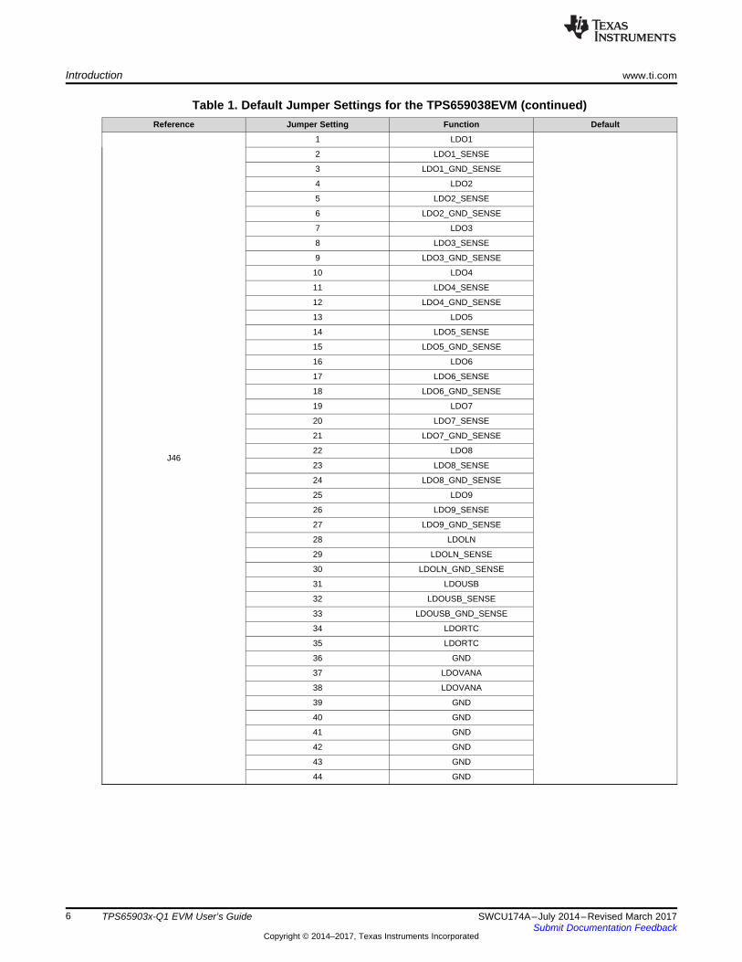
J46
1 LDO1
2 LDO1_SENSE
3 LDO1_GND_SENSE
4 LDO2
5 LDO2_SENSE
6 LDO2_GND_SENSE
7 LDO3
8 LDO3_SENSE
9 LDO3_GND_SENSE
10 LDO4
11 LDO4_SENSE
12 LDO4_GND_SENSE
13 LDO5
14 LDO5_SENSE
15 LDO5_GND_SENSE
16 LDO6
17 LDO6_SENSE
18 LDO6_GND_SENSE
19 LDO7
20 LDO7_SENSE
21 LDO7_GND_SENSE
22 LDO8
23 LDO8_SENSE
24 LDO8_GND_SENSE
25 LDO9
26 LDO9_SENSE
27 LDO9_GND_SENSE
28 LDOLN
29 LDOLN_SENSE
30 LDOLN_GND_SENSE
31 LDOUSB
32 LDOUSB_SENSE
33 LDOUSB_GND_SENSE
34 LDORTC
35 LDORTC
36 GND
37 LDOVANA
38 LDOVANA
39 GND
40 GND
41 GND
42 GND
43 GND
44 GND
www.ti.com EVM Schematics
7SWCU174A–July 2014–Revised March 2017Submit Documentation Feedback
Copyright © 2014–2017, Texas Instruments Incorporated
TPS65903x-Q1 EVM User’s Guide
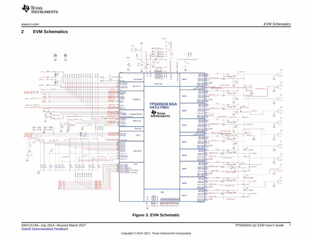
2 EVM Schematics
Figure 3. EVM Schematic

GND
GND
GND
GND GND
GNDGND
GND
GND GND
GND GND
GND GND
GNDGND
+5V
+5V
+3V3
+1V8
+3V3 +3V3
+3V3 +3V3
GND
GND
GND
+3V3
+3V3
GND GND
GND
GND
GND
GND
GND
+3V3
+5V
+3V3
+3V3
+3V3
GND
GNDGND
GND
GND
GNDGND
GNDGND
GND
GND
GND
GND
GND
GND
GND
GND
GND
+3V3
GND
+3V3
LDORTCBOOT0BOOT1GPIO_1
TESTVI2C2_SCLI2C2_SDA
SCLK
SIMO
CS
VIO_IN
I2C1_SCL
I2C1_SDA
I2C2_SCL
I2C2_SDA
I2C_SCL_MSP
I2C_SDA_MSP
I2C_SCL_MSP
I2C_SDA_MSP
VIO_IN
INT
ENABLE1
SOMI
IO8
IO3
IO7
NSLEEP
NRESWARM
RESET_IN
PWRDOWN
IO10
IO11
IO12
IO9
VIO_IN
SOMI
SIMO
SCLK
I2C_SCL_MSP
I2C_SDA_MSP
VIO_IN
RESET_OUT
LDORTC POWERGOOD
IO9
IO8
IO11
IO10
IO12
IO7 CS IO3
SMPS123GPADC_IN0GPADC_IN1GPADC_IN2GPADC_VREF
SMPS3POWERGOOD
SMPS45CLK32KGAO
SMPS6 LDORTCBOOT0
SMPS7 LDORTCBOOT1
GPIO_0GPIO_1GPIO_2GPIO_3GPIO_4GPIO_5GPIO_6GPIO_7REGEN1RESET_OUTLDORTC
SMPS8
SMPS9
VSYSPWRON
VSYSRPWRON
VSYS
VIO_IN_TPSVIO_IN
VIO_INSMPS7VIO_INSMPS9VIO_INLDO5VIO_INLDO3VIO_IN+1V8
LDO1LDO1
LDO2LDO2
LDO3LDO3
LDO4LDO4
LDO5LDO5
LDO6LDO6
LDO7LDO7
LDO8LDO8
LDO9LDO9
LDOLNLDOLN
LDOUSBLDOUSB
LDORTCLDORTC
LDOVANALDOVANA
SMPS1_2_FDBKSMPS12_GND_FB
SMPS3_FDBK
SMPS4_5_FDBKSMPS4_5_FDBK_GND
VIO_IN
SMPS6_FDBK
SMPS7_FDBK
SMPS8_FDBK
SMPS9_FDBK
GPIO_2GPIO_3
R71
1.5K
R79 0
J6
1234
R68 10k
J27
123456789101112
J26
123
R73
1.5K
Q2
J24
12
100nF
C58
J46
1234567891011121314151617181920212223242526272829303132333435363738394041424344
45
46
R85 0
R74
1.5K
VR4
2 1DIR
3 2DIR
4 1A1
5 1A2
6 2A1
7 2A2
8 GND 9GND1
102B2
112B1
121B2
131B1
14~2OE
15~1OE
16VCCB1 VCCA
470nF
C57
J15
1234
VR5
2 1DIR
3 2DIR
4 1A1
5 1A2
6 2A1
7 2A2
8 GND 9GND1
102B2
112B1
121B2
131B1
14~2OE
15~1OE
16VCCB1 VCCA
VR1
IN1
GND2
EN3
NC/FB4
OUT5
R75
120K
R88
1.5K
J48
12
J30
12
100nF
C56
R83 0
Y2
24Mhz
U2
MSP430F552XIPN
P6.4/CB4/A41
P6.5/CB5/A52
P6.6/CB6/A63
P6.7/CB7/A74
P7.0/CB8/A125
P7.1/CB9/A136
P7.2/CB10/A147
P7.3/CB11/A158
P5.0/VREF+/VEREF+9
P5.1/VREF-/VEREF-10
AVCC111
P5.4/XIN12
P5.5/XOUT13
AVSS114
P8.015
P8.116
P8.217
DVCC118
DVSS119
VCORE20
P1
.0/T
A0
CL
K/A
CL
K2
1
P1
.1/T
A0
.02
2
P1
.2/T
A0
.12
3
P1
.3/T
A0
.22
4
P1
.4/T
A0
.32
5
P1
.5/T
A0
.42
6
P1
.6/T
A1
CL
K/C
BO
UT
27
P1
.7/T
A1
.02
8
P2
.0/T
A1
.12
9
P2
.1/T
A1
.23
0
P2
.2/T
A2
CL
K/S
MC
LK
31
P2
.3/T
A2
.03
2
P2
.4/T
A2
.13
3
P2
.5/T
A2
.23
4
P2
.6/R
TC
CL
K/D
MA
E0
35
P2
.7/U
CB
0/S
TE
UC
A0
CL
K3
6
P3
.0/U
CB
0S
IMO
/UC
B0
SD
37
P3
.1/U
CB
0S
OM
I/U
CB
0S
C3
8
P3
.2/U
CB
0C
LK
/UC
A0
ST
E3
9
P3
,3/U
CA
0T
XD
/UC
A0
SIM
40
P3.4/UCA0RXD/UCA0SOM41
P3.5/TB0.542
P3.6/TB0.643
P3.7/TB0OUTH/SVMOUT44
P4.0/PM_UCB1STE/PM_U45
P4.1/PM_UCB1SIMO46
P4.2/PM_UCB1SOMI47
P4.3/PM_UCB1CLK48
DVSS249
DVCC250
P4.4/PM_UCA1TXD51
P4.5/PM_UCA1RXD52
P4.6/PM_NONE53
P4.7/PM_NONE54
P5.6/TB0.055
P5.7/TB0.156
P7.4/TB0.257
P7.5/TB0.358
P7.6/TB0.459
P7.7/TB0CLK/MCLK60
VS
SU
61
PU
.0/D
P6
2
PU
R6
3
PU
.1/D
M6
4
VB
US
65
VU
SB
66
V1
86
7
AV
SS
26
8
P5
.2/X
T2
IN6
9
P5
.3/X
T2
OU
T7
0
TE
ST
/SB
WT
CK
71
PJ.0
/TD
O7
2
PJ.1
/TD
I/T
CL
K7
3
PJ.2
/TM
S7
4
PJ.3
/TC
K7
5
NM
I/S
BW
TD
IO/R
ST
76
P6
.0/C
B0
/A0
77
P6
.1/C
B1
/A1
78
P6
.2/C
B2
/A2
79
P6
.3/C
B3
/A3
80
R87
1.5K
100pF
C54
4.7uF
C49
R81 0
100 nF
C48
D2
LED
100nF
C55
J29
123
4.7uF
C47
R9510K
J25
123
J22
1234
R67 10k
R69 10k
22pFC52
100 nF
C46
1nF
C50
Q1
VR3
2 1DIR
3 2DIR
4 1A1
5 1A2
6 2A1
7 2A2
8 GND 9GND1
102B2
112B1
121B2
131B1
14~2OE
15~1OE
16VCCB1 VCCA
J31
123456789101112
22pFC51
D3
LED
J32
123456789
10
J23
12
D4
LED
J14
1234
R90
2.2K
J16
1234
J17
1234
D1
LED
Q3
R89
2.2K
VR2
IN1
GND2
EN3
NC/FB4
OUT5
R7833
R761.5K R86 0
Q4
R7733
Q6
100pF
C53
J33
12
R84 0
J18
1234
J1
1
2
3
4
5 8
10
11
7
9
6
Q5
R70 10k
R72
1.5K
J28
123
R80 0
J20
1234
R82 0
J19
1234
EVM Schematics www.ti.com
8 SWCU174A–July 2014–Revised March 2017Submit Documentation Feedback
Copyright © 2014–2017, Texas Instruments Incorporated
TPS65903x-Q1 EVM User’s Guide
Figure 4. EVM Schematic
www.ti.com EVM BOM
9SWCU174A–July 2014–Revised March 2017Submit Documentation Feedback
Copyright © 2014–2017, Texas Instruments Incorporated
TPS65903x-Q1 EVM User’s Guide
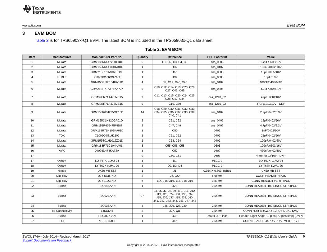
3 EVM BOMTable 2 is for TPS65903x-Q1 EVM. The latest BOM is included in the TPS65903x-Q1 data sheet.
Table 2. EVM BOMItem Manufacturer Manufacturer Part No. Quantity Reference PCB Footprint Value
1 Murata GRM188R61A225KE34D 5 C1, C2, C3, C4, C5 cns_0603 2.2µF/0603/10V
2 Murata GRM155R61A104KA01D 1 C6 cns_0402 100nF/0402/10V
3 Murata GRM21BR61A106KE19L 1 C7 cns_0805 10µF/0805/10V
4 KEMET C0603C106M9PAC 1 C8 cns_0603 10µF/6.3V
5 Murata GRM155R60J104KA01D 4 C9, C17, C46, C48 cns_0402 100nF/0402/6.3V
6 Murata GRM21BR71A475KA73K 9 C10, C12, C14, C19, C23, C26,C27, C43, C45 cns_0805 4.7µF/0805/10V
7 Murata GRM32ER71A476ME15 9 C11, C13, C15, C20, C24, C25,C28, C42, C44 cns_1210_02 47µF/1210/10V
8 Murata GRM32ER71A476ME15 0 C16, C59 cns_1210_02 47µF/1210/10V - DNP
9 Murata GRM155R60J225ME15D 14C18, C29, C30, C31, C32, C33,C34, C35, C36, C37, C38, C39,
C40, C41cns_0402 2.2µF/0402/6.3V
10 Murata GRM155C1H120GA01D 2 C21, C22 cns_0402 12pF/0402/50V
11 Murata GRM155R60J475ME87 2 C47, C49 cns_0402 4.7µF/0402/6.3V
12 Murata GRM155R71H102KA01D 1 C50 0402 1nF/0402/50V
13 TDK C1005C0G1H220J 2 C51, C52 0402 22pF/0402/50V
14 Murata GRM1555C1H101JZ01D 2 C53, C54 0402 100pF/0402/50V
15 Murata GRM188R71C104KA01 3 C55, C56, C58 0603 100nF/0603/16V
16 AVX 04026D474KAT2A 1 C57 0402 470nF/0402/50V
17 0 C60, C61 0603 4.7nF/0603/16V - DNP
17 Osram LO T67K-L1M2 24 1 D1 PLCC-2 LO T67K-L1M2-24
18 Osram LY T67K-K2M1 26 3 D2, D3, D4 PLCC-2 LY T67K-K2M1 26
19 Hirose UX60-MB-5ST 1 J1 0.354 X 0.303 Inches UX60-MB-5ST
20 Digi-Key 277-6735-ND 2 J6, J20 5.08MM CONN HEADER 4POS
21 Digi-Key 277-1223-ND 6 J14, J15, J16, J17, J18, J19 3.81MM CONN HEADER VERT 4POS
22 Sullins PEC04SAAN 1 J22 2.54MM CONN HEADER .100 SINGL STR 4POS
23 Sullins PEC02SAAN 27
J3, J5, J7, J8, J9, J10, J11, J12,J13, J23, J24, J30, J33, J34,J35, J36, J37, J38, J39, J40,
J41, J42, J43, J44, J45, J47, J48
2.54MM CONN HEADER .100 SINGL STR 2POS
24 Sullins PEC03SAAN 4 J25, J26, J28, J29 2.54MM CONN HEADER .100 SINGL STR 3POS
25 TE Connectivity 146130-5 2 J27, J31 2.54MM CONN HDR BRKWAY 12POS DUAL SMD
26 Sullins PEC36DBAN 1 J32 .500 x .378 inch Header, Right Angle 10 pins [72 pins strip] (DNP)
27 FCI 71918-144LF 1 J46 2.54MM CONN HEADER 44POS DUAL VERT PCB
EVM BOM www.ti.com
10 SWCU174A–July 2014–Revised March 2017Submit Documentation Feedback
Copyright © 2014–2017, Texas Instruments Incorporated
TPS65903x-Q1 EVM User’s Guide
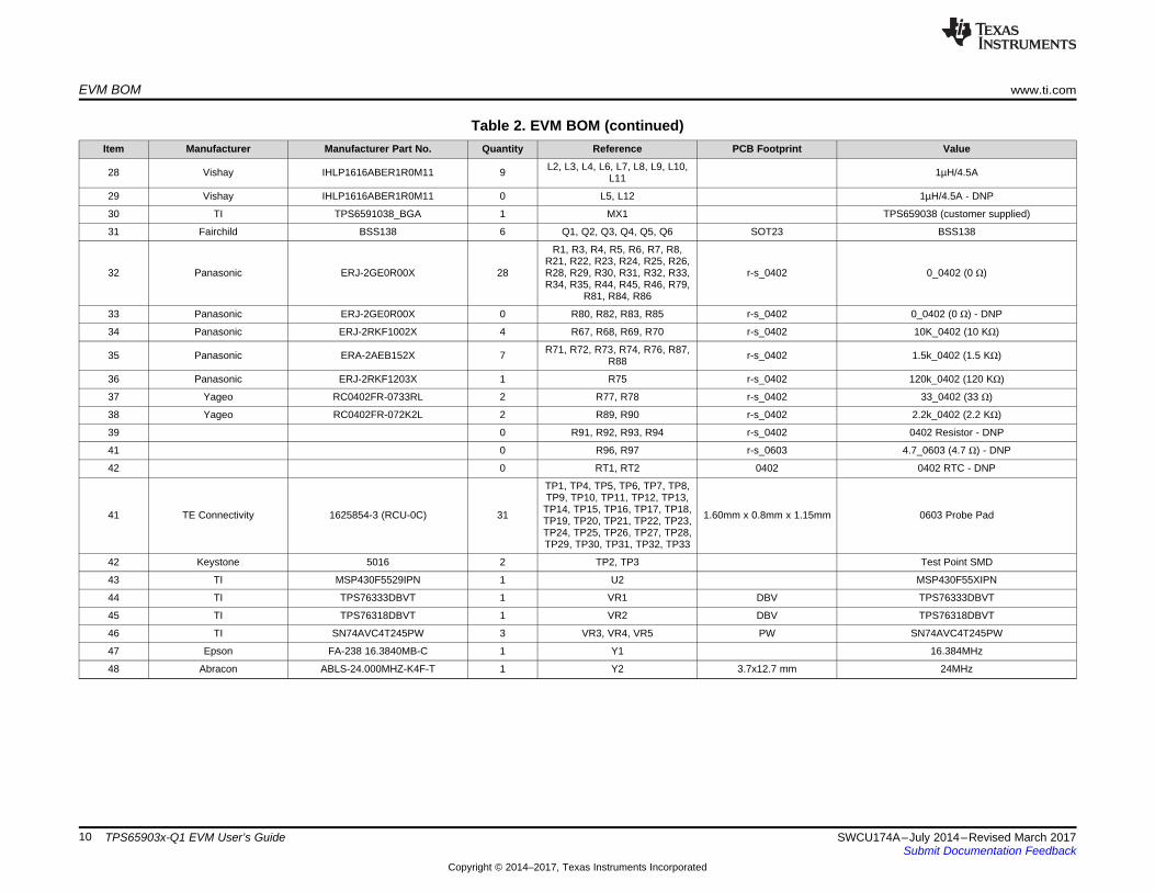
Table 2. EVM BOM (continued)Item Manufacturer Manufacturer Part No. Quantity Reference PCB Footprint Value
28 Vishay IHLP1616ABER1R0M11 9 L2, L3, L4, L6, L7, L8, L9, L10,L11 1µH/4.5A
29 Vishay IHLP1616ABER1R0M11 0 L5, L12 1µH/4.5A - DNP
30 TI TPS6591038_BGA 1 MX1 TPS659038 (customer supplied)
31 Fairchild BSS138 6 Q1, Q2, Q3, Q4, Q5, Q6 SOT23 BSS138
32 Panasonic ERJ-2GE0R00X 28
R1, R3, R4, R5, R6, R7, R8,R21, R22, R23, R24, R25, R26,R28, R29, R30, R31, R32, R33,R34, R35, R44, R45, R46, R79,
R81, R84, R86
r-s_0402 0_0402 (0 Ω)
33 Panasonic ERJ-2GE0R00X 0 R80, R82, R83, R85 r-s_0402 0_0402 (0 Ω) - DNP
34 Panasonic ERJ-2RKF1002X 4 R67, R68, R69, R70 r-s_0402 10K_0402 (10 KΩ)
35 Panasonic ERA-2AEB152X 7 R71, R72, R73, R74, R76, R87,R88 r-s_0402 1.5k_0402 (1.5 KΩ)
36 Panasonic ERJ-2RKF1203X 1 R75 r-s_0402 120k_0402 (120 KΩ)
37 Yageo RC0402FR-0733RL 2 R77, R78 r-s_0402 33_0402 (33 Ω)
38 Yageo RC0402FR-072K2L 2 R89, R90 r-s_0402 2.2k_0402 (2.2 KΩ)
39 0 R91, R92, R93, R94 r-s_0402 0402 Resistor - DNP
41 0 R96, R97 r-s_0603 4.7_0603 (4.7 Ω) - DNP
42 0 RT1, RT2 0402 0402 RTC - DNP
41 TE Connectivity 1625854-3 (RCU-0C) 31
TP1, TP4, TP5, TP6, TP7, TP8,TP9, TP10, TP11, TP12, TP13,TP14, TP15, TP16, TP17, TP18,TP19, TP20, TP21, TP22, TP23,TP24, TP25, TP26, TP27, TP28,TP29, TP30, TP31, TP32, TP33
1.60mm x 0.8mm x 1.15mm 0603 Probe Pad
42 Keystone 5016 2 TP2, TP3 Test Point SMD
43 TI MSP430F5529IPN 1 U2 MSP430F55XIPN
44 TI TPS76333DBVT 1 VR1 DBV TPS76333DBVT
45 TI TPS76318DBVT 1 VR2 DBV TPS76318DBVT
46 TI SN74AVC4T245PW 3 VR3, VR4, VR5 PW SN74AVC4T245PW
47 Epson FA-238 16.3840MB-C 1 Y1 16.384MHz
48 Abracon ABLS-24.000MHZ-K4F-T 1 Y2 3.7x12.7 mm 24MHz
www.ti.com Powering up the Device
11SWCU174A–July 2014–Revised March 2017Submit Documentation Feedback
Copyright © 2014–2017, Texas Instruments Incorporated
TPS65903x-Q1 EVM User’s Guide
4 Powering up the Device
To turn on the device, perform the following steps:1. Turn off the supply voltage, unplug the USB, and close the GUI.2. While the power supply is disabled, connect it to the EVM through the J20 connector.3. Plug the USB cable to the EVM and the computer. The MSP430 LED should blink a few times and
then stay on.4. Set the power supply to a voltage between 3.135 V and 5.25 V. Turn on the supply voltage. The
LDORTC LED should light up.5. Launch the GUI on the computer. All sequenced rails will power up to the predefined voltage.6. Under the DUT_Control tab, send a logic high signal to the RESET_IN pin by checking the box next to
RESET_IN and clicking Write Static. The RESET_OUT LED should light up, and the PMIC is nowenabled.
TPS65903x-Q1EVM Graphical User Interface (GUI) www.ti.com
12 SWCU174A–July 2014–Revised March 2017Submit Documentation Feedback
Copyright © 2014–2017, Texas Instruments Incorporated
TPS65903x-Q1 EVM User’s Guide
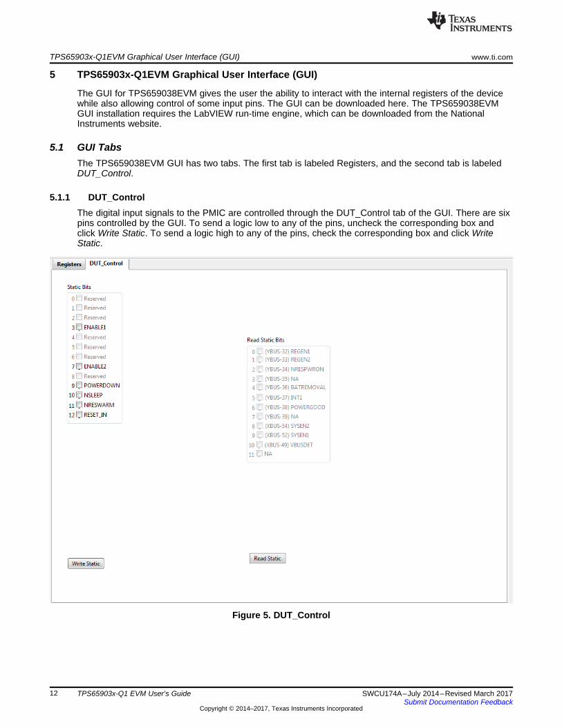
5 TPS65903x-Q1EVM Graphical User Interface (GUI)
The GUI for TPS659038EVM gives the user the ability to interact with the internal registers of the devicewhile also allowing control of some input pins. The GUI can be downloaded here. The TPS659038EVMGUI installation requires the LabVIEW run-time engine, which can be downloaded from the NationalInstruments website.
5.1 GUI TabsThe TPS659038EVM GUI has two tabs. The first tab is labeled Registers, and the second tab is labeledDUT_Control.
5.1.1 DUT_ControlThe digital input signals to the PMIC are controlled through the DUT_Control tab of the GUI. There are sixpins controlled by the GUI. To send a logic low to any of the pins, uncheck the corresponding box andclick Write Static. To send a logic high to any of the pins, check the corresponding box and click WriteStatic.
Figure 5. DUT_Control
www.ti.com TPS65903x-Q1EVM Graphical User Interface (GUI)
13SWCU174A–July 2014–Revised March 2017Submit Documentation Feedback
Copyright © 2014–2017, Texas Instruments Incorporated
TPS65903x-Q1 EVM User’s Guide
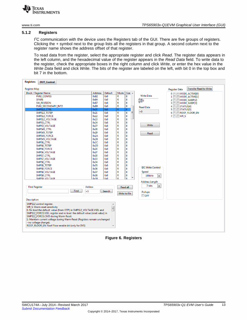
5.1.2 RegistersI2C communication with the device uses the Registers tab of the GUI. There are five groups of registers.Clicking the + symbol next to the group lists all the registers in that group. A second column next to theregister name shows the address offset of that register.
To read data from the register, select the appropriate register and click Read. The register data appears inthe left column, and the hexadecimal value of the register appears in the Read Data field. To write data tothe register, check the appropriate boxes in the right column and click Write, or enter the hex value in theWrite Data field and click Write. The bits of the register are labeled on the left, with bit 0 in the top box andbit 7 in the bottom.
Figure 6. Registers
TPS65903x-Q1EVM Graphical User Interface (GUI) www.ti.com
14 SWCU174A–July 2014–Revised March 2017Submit Documentation Feedback
Copyright © 2014–2017, Texas Instruments Incorporated
TPS65903x-Q1 EVM User’s Guide
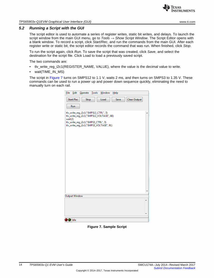
5.2 Running a Script with the GUIThe script editor is used to automate a series of register writes, static bit writes, and delays. To launch thescript window from the main GUI menu, go to Tools → Show Script Window. The Script Editor opens witha blank window. To record a script, click Start/Rec, and run the commands from the main GUI. After eachregister write or static bit, the script editor records the command that was run. When finished, click Stop.
To run the script again, click Run. To save the script that was created, click Save, and select thedestination for the script file. Click Load to load a previously saved script.
The two commands are:• tlv_write_reg_i2c1(REGISTER_NAME, VALUE), where the value is the decimal value to write.• wait(TIME_IN_MS)
The script in Figure 7 turns on SMPS12 to 1.1 V, waits 2 ms, and then turns on SMPS3 to 1.35 V. Thesecommands can be used to run a power up and power down sequence quickly, eliminating the need tomanually turn on each rail.
Figure 7. Sample Script

www.ti.com Revision History
15SWCU174A–July 2014–Revised March 2017Submit Documentation Feedback
Copyright © 2014–2017, Texas Instruments Incorporated
Revision History
Revision HistoryNOTE: Page numbers for previous revisions may differ from page numbers in the current version.
Changes from Original (July 2014) to A Revision ........................................................................................................... Page
• First public release of document ........................................................................................................ 1
STANDARD TERMS FOR EVALUATION MODULES1. Delivery: TI delivers TI evaluation boards, kits, or modules, including any accompanying demonstration software, components, and/or
documentation which may be provided together or separately (collectively, an “EVM” or “EVMs”) to the User (“User”) in accordancewith the terms set forth herein. User's acceptance of the EVM is expressly subject to the following terms.1.1 EVMs are intended solely for product or software developers for use in a research and development setting to facilitate feasibility
evaluation, experimentation, or scientific analysis of TI semiconductors products. EVMs have no direct function and are notfinished products. EVMs shall not be directly or indirectly assembled as a part or subassembly in any finished product. Forclarification, any software or software tools provided with the EVM (“Software”) shall not be subject to the terms and conditionsset forth herein but rather shall be subject to the applicable terms that accompany such Software
1.2 EVMs are not intended for consumer or household use. EVMs may not be sold, sublicensed, leased, rented, loaned, assigned,or otherwise distributed for commercial purposes by Users, in whole or in part, or used in any finished product or productionsystem.
2 Limited Warranty and Related Remedies/Disclaimers:2.1 These terms do not apply to Software. The warranty, if any, for Software is covered in the applicable Software License
Agreement.2.2 TI warrants that the TI EVM will conform to TI's published specifications for ninety (90) days after the date TI delivers such EVM
to User. Notwithstanding the foregoing, TI shall not be liable for a nonconforming EVM if (a) the nonconformity was caused byneglect, misuse or mistreatment by an entity other than TI, including improper installation or testing, or for any EVMs that havebeen altered or modified in any way by an entity other than TI, (b) the nonconformity resulted from User's design, specificationsor instructions for such EVMs or improper system design, or (c) User has not paid on time. Testing and other quality controltechniques are used to the extent TI deems necessary. TI does not test all parameters of each EVM.User's claims against TI under this Section 2 are void if User fails to notify TI of any apparent defects in the EVMs within ten (10)business days after delivery, or of any hidden defects with ten (10) business days after the defect has been detected.
2.3 TI's sole liability shall be at its option to repair or replace EVMs that fail to conform to the warranty set forth above, or creditUser's account for such EVM. TI's liability under this warranty shall be limited to EVMs that are returned during the warrantyperiod to the address designated by TI and that are determined by TI not to conform to such warranty. If TI elects to repair orreplace such EVM, TI shall have a reasonable time to repair such EVM or provide replacements. Repaired EVMs shall bewarranted for the remainder of the original warranty period. Replaced EVMs shall be warranted for a new full ninety (90) daywarranty period.
3 Regulatory Notices:3.1 United States
3.1.1 Notice applicable to EVMs not FCC-Approved:FCC NOTICE: This kit is designed to allow product developers to evaluate electronic components, circuitry, or softwareassociated with the kit to determine whether to incorporate such items in a finished product and software developers to writesoftware applications for use with the end product. This kit is not a finished product and when assembled may not be resold orotherwise marketed unless all required FCC equipment authorizations are first obtained. Operation is subject to the conditionthat this product not cause harmful interference to licensed radio stations and that this product accept harmful interference.Unless the assembled kit is designed to operate under part 15, part 18 or part 95 of this chapter, the operator of the kit mustoperate under the authority of an FCC license holder or must secure an experimental authorization under part 5 of this chapter.3.1.2 For EVMs annotated as FCC – FEDERAL COMMUNICATIONS COMMISSION Part 15 Compliant:
CAUTIONThis device complies with part 15 of the FCC Rules. Operation is subject to the following two conditions: (1) This device may notcause harmful interference, and (2) this device must accept any interference received, including interference that may causeundesired operation.Changes or modifications not expressly approved by the party responsible for compliance could void the user's authority tooperate the equipment.
FCC Interference Statement for Class A EVM devicesNOTE: This equipment has been tested and found to comply with the limits for a Class A digital device, pursuant to part 15 ofthe FCC Rules. These limits are designed to provide reasonable protection against harmful interference when the equipment isoperated in a commercial environment. This equipment generates, uses, and can radiate radio frequency energy and, if notinstalled and used in accordance with the instruction manual, may cause harmful interference to radio communications.Operation of this equipment in a residential area is likely to cause harmful interference in which case the user will be required tocorrect the interference at his own expense.

FCC Interference Statement for Class B EVM devicesNOTE: This equipment has been tested and found to comply with the limits for a Class B digital device, pursuant to part 15 ofthe FCC Rules. These limits are designed to provide reasonable protection against harmful interference in a residentialinstallation. This equipment generates, uses and can radiate radio frequency energy and, if not installed and used in accordancewith the instructions, may cause harmful interference to radio communications. However, there is no guarantee that interferencewill not occur in a particular installation. If this equipment does cause harmful interference to radio or television reception, whichcan be determined by turning the equipment off and on, the user is encouraged to try to correct the interference by one or moreof the following measures:
• Reorient or relocate the receiving antenna.• Increase the separation between the equipment and receiver.• Connect the equipment into an outlet on a circuit different from that to which the receiver is connected.• Consult the dealer or an experienced radio/TV technician for help.
3.2 Canada3.2.1 For EVMs issued with an Industry Canada Certificate of Conformance to RSS-210 or RSS-247
Concerning EVMs Including Radio Transmitters:This device complies with Industry Canada license-exempt RSSs. Operation is subject to the following two conditions:(1) this device may not cause interference, and (2) this device must accept any interference, including interference that maycause undesired operation of the device.
Concernant les EVMs avec appareils radio:Le présent appareil est conforme aux CNR d'Industrie Canada applicables aux appareils radio exempts de licence. L'exploitationest autorisée aux deux conditions suivantes: (1) l'appareil ne doit pas produire de brouillage, et (2) l'utilisateur de l'appareil doitaccepter tout brouillage radioélectrique subi, même si le brouillage est susceptible d'en compromettre le fonctionnement.
Concerning EVMs Including Detachable Antennas:Under Industry Canada regulations, this radio transmitter may only operate using an antenna of a type and maximum (or lesser)gain approved for the transmitter by Industry Canada. To reduce potential radio interference to other users, the antenna typeand its gain should be so chosen that the equivalent isotropically radiated power (e.i.r.p.) is not more than that necessary forsuccessful communication. This radio transmitter has been approved by Industry Canada to operate with the antenna typeslisted in the user guide with the maximum permissible gain and required antenna impedance for each antenna type indicated.Antenna types not included in this list, having a gain greater than the maximum gain indicated for that type, are strictly prohibitedfor use with this device.
Concernant les EVMs avec antennes détachablesConformément à la réglementation d'Industrie Canada, le présent émetteur radio peut fonctionner avec une antenne d'un type etd'un gain maximal (ou inférieur) approuvé pour l'émetteur par Industrie Canada. Dans le but de réduire les risques de brouillageradioélectrique à l'intention des autres utilisateurs, il faut choisir le type d'antenne et son gain de sorte que la puissance isotroperayonnée équivalente (p.i.r.e.) ne dépasse pas l'intensité nécessaire à l'établissement d'une communication satisfaisante. Leprésent émetteur radio a été approuvé par Industrie Canada pour fonctionner avec les types d'antenne énumérés dans lemanuel d’usage et ayant un gain admissible maximal et l'impédance requise pour chaque type d'antenne. Les types d'antennenon inclus dans cette liste, ou dont le gain est supérieur au gain maximal indiqué, sont strictement interdits pour l'exploitation del'émetteur
3.3 Japan3.3.1 Notice for EVMs delivered in Japan: Please see http://www.tij.co.jp/lsds/ti_ja/general/eStore/notice_01.page 日本国内に
輸入される評価用キット、ボードについては、次のところをご覧ください。http://www.tij.co.jp/lsds/ti_ja/general/eStore/notice_01.page
3.3.2 Notice for Users of EVMs Considered “Radio Frequency Products” in Japan: EVMs entering Japan may not be certifiedby TI as conforming to Technical Regulations of Radio Law of Japan.
If User uses EVMs in Japan, not certified to Technical Regulations of Radio Law of Japan, User is required to follow theinstructions set forth by Radio Law of Japan, which includes, but is not limited to, the instructions below with respect to EVMs(which for the avoidance of doubt are stated strictly for convenience and should be verified by User):1. Use EVMs in a shielded room or any other test facility as defined in the notification #173 issued by Ministry of Internal
Affairs and Communications on March 28, 2006, based on Sub-section 1.1 of Article 6 of the Ministry’s Rule forEnforcement of Radio Law of Japan,
2. Use EVMs only after User obtains the license of Test Radio Station as provided in Radio Law of Japan with respect toEVMs, or
3. Use of EVMs only after User obtains the Technical Regulations Conformity Certification as provided in Radio Law of Japanwith respect to EVMs. Also, do not transfer EVMs, unless User gives the same notice above to the transferee. Please notethat if User does not follow the instructions above, User will be subject to penalties of Radio Law of Japan.
【無線電波を送信する製品の開発キットをお使いになる際の注意事項】 開発キットの中には技術基準適合証明を受けていないものがあります。 技術適合証明を受けていないもののご使用に際しては、電波法遵守のため、以下のいずれかの措置を取っていただく必要がありますのでご注意ください。1. 電波法施行規則第6条第1項第1号に基づく平成18年3月28日総務省告示第173号で定められた電波暗室等の試験設備でご使用
いただく。2. 実験局の免許を取得後ご使用いただく。3. 技術基準適合証明を取得後ご使用いただく。
なお、本製品は、上記の「ご使用にあたっての注意」を譲渡先、移転先に通知しない限り、譲渡、移転できないものとします。上記を遵守頂けない場合は、電波法の罰則が適用される可能性があることをご留意ください。 日本テキサス・イ
ンスツルメンツ株式会社東京都新宿区西新宿6丁目24番1号西新宿三井ビル
3.3.3 Notice for EVMs for Power Line Communication: Please see http://www.tij.co.jp/lsds/ti_ja/general/eStore/notice_02.page電力線搬送波通信についての開発キットをお使いになる際の注意事項については、次のところをご覧ください。http://www.tij.co.jp/lsds/ti_ja/general/eStore/notice_02.page
3.4 European Union3.4.1 For EVMs subject to EU Directive 2014/30/EU (Electromagnetic Compatibility Directive):
This is a class A product intended for use in environments other than domestic environments that are connected to alow-voltage power-supply network that supplies buildings used for domestic purposes. In a domestic environment thisproduct may cause radio interference in which case the user may be required to take adequate measures.
4 EVM Use Restrictions and Warnings:4.1 EVMS ARE NOT FOR USE IN FUNCTIONAL SAFETY AND/OR SAFETY CRITICAL EVALUATIONS, INCLUDING BUT NOT
LIMITED TO EVALUATIONS OF LIFE SUPPORT APPLICATIONS.4.2 User must read and apply the user guide and other available documentation provided by TI regarding the EVM prior to handling
or using the EVM, including without limitation any warning or restriction notices. The notices contain important safety informationrelated to, for example, temperatures and voltages.
4.3 Safety-Related Warnings and Restrictions:4.3.1 User shall operate the EVM within TI’s recommended specifications and environmental considerations stated in the user
guide, other available documentation provided by TI, and any other applicable requirements and employ reasonable andcustomary safeguards. Exceeding the specified performance ratings and specifications (including but not limited to inputand output voltage, current, power, and environmental ranges) for the EVM may cause personal injury or death, orproperty damage. If there are questions concerning performance ratings and specifications, User should contact a TIfield representative prior to connecting interface electronics including input power and intended loads. Any loads appliedoutside of the specified output range may also result in unintended and/or inaccurate operation and/or possiblepermanent damage to the EVM and/or interface electronics. Please consult the EVM user guide prior to connecting anyload to the EVM output. If there is uncertainty as to the load specification, please contact a TI field representative.During normal operation, even with the inputs and outputs kept within the specified allowable ranges, some circuitcomponents may have elevated case temperatures. These components include but are not limited to linear regulators,switching transistors, pass transistors, current sense resistors, and heat sinks, which can be identified using theinformation in the associated documentation. When working with the EVM, please be aware that the EVM may becomevery warm.
4.3.2 EVMs are intended solely for use by technically qualified, professional electronics experts who are familiar with thedangers and application risks associated with handling electrical mechanical components, systems, and subsystems.User assumes all responsibility and liability for proper and safe handling and use of the EVM by User or its employees,affiliates, contractors or designees. User assumes all responsibility and liability to ensure that any interfaces (electronicand/or mechanical) between the EVM and any human body are designed with suitable isolation and means to safelylimit accessible leakage currents to minimize the risk of electrical shock hazard. User assumes all responsibility andliability for any improper or unsafe handling or use of the EVM by User or its employees, affiliates, contractors ordesignees.
4.4 User assumes all responsibility and liability to determine whether the EVM is subject to any applicable international, federal,state, or local laws and regulations related to User’s handling and use of the EVM and, if applicable, User assumes allresponsibility and liability for compliance in all respects with such laws and regulations. User assumes all responsibility andliability for proper disposal and recycling of the EVM consistent with all applicable international, federal, state, and localrequirements.
5. Accuracy of Information: To the extent TI provides information on the availability and function of EVMs, TI attempts to be as accurateas possible. However, TI does not warrant the accuracy of EVM descriptions, EVM availability or other information on its websites asaccurate, complete, reliable, current, or error-free.
6. Disclaimers:6.1 EXCEPT AS SET FORTH ABOVE, EVMS AND ANY MATERIALS PROVIDED WITH THE EVM (INCLUDING, BUT NOT
LIMITED TO, REFERENCE DESIGNS AND THE DESIGN OF THE EVM ITSELF) ARE PROVIDED "AS IS" AND "WITH ALLFAULTS." TI DISCLAIMS ALL OTHER WARRANTIES, EXPRESS OR IMPLIED, REGARDING SUCH ITEMS, INCLUDING BUTNOT LIMITED TO ANY EPIDEMIC FAILURE WARRANTY OR IMPLIED WARRANTIES OF MERCHANTABILITY OR FITNESSFOR A PARTICULAR PURPOSE OR NON-INFRINGEMENT OF ANY THIRD PARTY PATENTS, COPYRIGHTS, TRADESECRETS OR OTHER INTELLECTUAL PROPERTY RIGHTS.
6.2 EXCEPT FOR THE LIMITED RIGHT TO USE THE EVM SET FORTH HEREIN, NOTHING IN THESE TERMS SHALL BECONSTRUED AS GRANTING OR CONFERRING ANY RIGHTS BY LICENSE, PATENT, OR ANY OTHER INDUSTRIAL ORINTELLECTUAL PROPERTY RIGHT OF TI, ITS SUPPLIERS/LICENSORS OR ANY OTHER THIRD PARTY, TO USE THEEVM IN ANY FINISHED END-USER OR READY-TO-USE FINAL PRODUCT, OR FOR ANY INVENTION, DISCOVERY ORIMPROVEMENT, REGARDLESS OF WHEN MADE, CONCEIVED OR ACQUIRED.
7. USER'S INDEMNITY OBLIGATIONS AND REPRESENTATIONS. USER WILL DEFEND, INDEMNIFY AND HOLD TI, ITSLICENSORS AND THEIR REPRESENTATIVES HARMLESS FROM AND AGAINST ANY AND ALL CLAIMS, DAMAGES, LOSSES,EXPENSES, COSTS AND LIABILITIES (COLLECTIVELY, "CLAIMS") ARISING OUT OF OR IN CONNECTION WITH ANYHANDLING OR USE OF THE EVM THAT IS NOT IN ACCORDANCE WITH THESE TERMS. THIS OBLIGATION SHALL APPLYWHETHER CLAIMS ARISE UNDER STATUTE, REGULATION, OR THE LAW OF TORT, CONTRACT OR ANY OTHER LEGALTHEORY, AND EVEN IF THE EVM FAILS TO PERFORM AS DESCRIBED OR EXPECTED.
8. Limitations on Damages and Liability:8.1 General Limitations. IN NO EVENT SHALL TI BE LIABLE FOR ANY SPECIAL, COLLATERAL, INDIRECT, PUNITIVE,
INCIDENTAL, CONSEQUENTIAL, OR EXEMPLARY DAMAGES IN CONNECTION WITH OR ARISING OUT OF THESETERMS OR THE USE OF THE EVMS , REGARDLESS OF WHETHER TI HAS BEEN ADVISED OF THE POSSIBILITY OFSUCH DAMAGES. EXCLUDED DAMAGES INCLUDE, BUT ARE NOT LIMITED TO, COST OF REMOVAL ORREINSTALLATION, ANCILLARY COSTS TO THE PROCUREMENT OF SUBSTITUTE GOODS OR SERVICES, RETESTING,OUTSIDE COMPUTER TIME, LABOR COSTS, LOSS OF GOODWILL, LOSS OF PROFITS, LOSS OF SAVINGS, LOSS OFUSE, LOSS OF DATA, OR BUSINESS INTERRUPTION. NO CLAIM, SUIT OR ACTION SHALL BE BROUGHT AGAINST TIMORE THAN TWELVE (12) MONTHS AFTER THE EVENT THAT GAVE RISE TO THE CAUSE OF ACTION HASOCCURRED.
8.2 Specific Limitations. IN NO EVENT SHALL TI'S AGGREGATE LIABILITY FROM ANY USE OF AN EVM PROVIDEDHEREUNDER, INCLUDING FROM ANY WARRANTY, INDEMITY OR OTHER OBLIGATION ARISING OUT OF OR INCONNECTION WITH THESE TERMS, , EXCEED THE TOTAL AMOUNT PAID TO TI BY USER FOR THE PARTICULAREVM(S) AT ISSUE DURING THE PRIOR TWELVE (12) MONTHS WITH RESPECT TO WHICH LOSSES OR DAMAGES ARECLAIMED. THE EXISTENCE OF MORE THAN ONE CLAIM SHALL NOT ENLARGE OR EXTEND THIS LIMIT.
9. Return Policy. Except as otherwise provided, TI does not offer any refunds, returns, or exchanges. Furthermore, no return of EVM(s)will be accepted if the package has been opened and no return of the EVM(s) will be accepted if they are damaged or otherwise not ina resalable condition. If User feels it has been incorrectly charged for the EVM(s) it ordered or that delivery violates the applicableorder, User should contact TI. All refunds will be made in full within thirty (30) working days from the return of the components(s),excluding any postage or packaging costs.
10. Governing Law: These terms and conditions shall be governed by and interpreted in accordance with the laws of the State of Texas,without reference to conflict-of-laws principles. User agrees that non-exclusive jurisdiction for any dispute arising out of or relating tothese terms and conditions lies within courts located in the State of Texas and consents to venue in Dallas County, Texas.Notwithstanding the foregoing, any judgment may be enforced in any United States or foreign court, and TI may seek injunctive reliefin any United States or foreign court.
Mailing Address: Texas Instruments, Post Office Box 655303, Dallas, Texas 75265Copyright © 2017, Texas Instruments Incorporated
IMPORTANT NOTICE FOR TI DESIGN INFORMATION AND RESOURCES
Texas Instruments Incorporated (‘TI”) technical, application or other design advice, services or information, including, but not limited to,reference designs and materials relating to evaluation modules, (collectively, “TI Resources”) are intended to assist designers who aredeveloping applications that incorporate TI products; by downloading, accessing or using any particular TI Resource in any way, you(individually or, if you are acting on behalf of a company, your company) agree to use it solely for this purpose and subject to the terms ofthis Notice.TI’s provision of TI Resources does not expand or otherwise alter TI’s applicable published warranties or warranty disclaimers for TIproducts, and no additional obligations or liabilities arise from TI providing such TI Resources. TI reserves the right to make corrections,enhancements, improvements and other changes to its TI Resources.You understand and agree that you remain responsible for using your independent analysis, evaluation and judgment in designing yourapplications and that you have full and exclusive responsibility to assure the safety of your applications and compliance of your applications(and of all TI products used in or for your applications) with all applicable regulations, laws and other applicable requirements. Yourepresent that, with respect to your applications, you have all the necessary expertise to create and implement safeguards that (1)anticipate dangerous consequences of failures, (2) monitor failures and their consequences, and (3) lessen the likelihood of failures thatmight cause harm and take appropriate actions. You agree that prior to using or distributing any applications that include TI products, youwill thoroughly test such applications and the functionality of such TI products as used in such applications. TI has not conducted anytesting other than that specifically described in the published documentation for a particular TI Resource.You are authorized to use, copy and modify any individual TI Resource only in connection with the development of applications that includethe TI product(s) identified in such TI Resource. NO OTHER LICENSE, EXPRESS OR IMPLIED, BY ESTOPPEL OR OTHERWISE TOANY OTHER TI INTELLECTUAL PROPERTY RIGHT, AND NO LICENSE TO ANY TECHNOLOGY OR INTELLECTUAL PROPERTYRIGHT OF TI OR ANY THIRD PARTY IS GRANTED HEREIN, including but not limited to any patent right, copyright, mask work right, orother intellectual property right relating to any combination, machine, or process in which TI products or services are used. Informationregarding or referencing third-party products or services does not constitute a license to use such products or services, or a warranty orendorsement thereof. Use of TI Resources may require a license from a third party under the patents or other intellectual property of thethird party, or a license from TI under the patents or other intellectual property of TI.TI RESOURCES ARE PROVIDED “AS IS” AND WITH ALL FAULTS. TI DISCLAIMS ALL OTHER WARRANTIES ORREPRESENTATIONS, EXPRESS OR IMPLIED, REGARDING TI RESOURCES OR USE THEREOF, INCLUDING BUT NOT LIMITED TOACCURACY OR COMPLETENESS, TITLE, ANY EPIDEMIC FAILURE WARRANTY AND ANY IMPLIED WARRANTIES OFMERCHANTABILITY, FITNESS FOR A PARTICULAR PURPOSE, AND NON-INFRINGEMENT OF ANY THIRD PARTY INTELLECTUALPROPERTY RIGHTS.TI SHALL NOT BE LIABLE FOR AND SHALL NOT DEFEND OR INDEMNIFY YOU AGAINST ANY CLAIM, INCLUDING BUT NOTLIMITED TO ANY INFRINGEMENT CLAIM THAT RELATES TO OR IS BASED ON ANY COMBINATION OF PRODUCTS EVEN IFDESCRIBED IN TI RESOURCES OR OTHERWISE. IN NO EVENT SHALL TI BE LIABLE FOR ANY ACTUAL, DIRECT, SPECIAL,COLLATERAL, INDIRECT, PUNITIVE, INCIDENTAL, CONSEQUENTIAL OR EXEMPLARY DAMAGES IN CONNECTION WITH ORARISING OUT OF TI RESOURCES OR USE THEREOF, AND REGARDLESS OF WHETHER TI HAS BEEN ADVISED OF THEPOSSIBILITY OF SUCH DAMAGES.You agree to fully indemnify TI and its representatives against any damages, costs, losses, and/or liabilities arising out of your non-compliance with the terms and provisions of this Notice.This Notice applies to TI Resources. Additional terms apply to the use and purchase of certain types of materials, TI products and services.These include; without limitation, TI’s standard terms for semiconductor products http://www.ti.com/sc/docs/stdterms.htm), evaluationmodules, and samples (http://www.ti.com/sc/docs/sampterms.htm).
Mailing Address: Texas Instruments, Post Office Box 655303, Dallas, Texas 75265Copyright © 2017, Texas Instruments Incorporated
Related Documents