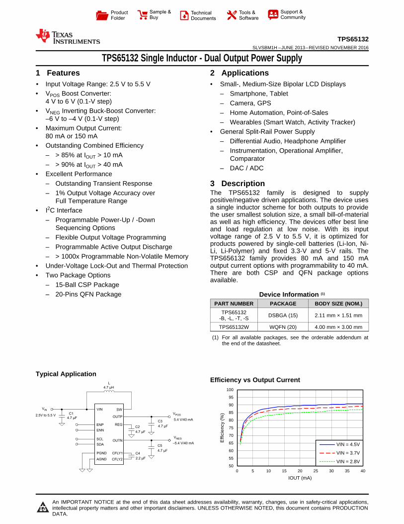
50 55 60 65 70 75 80 85 90 95 100 0 5 10 15 20 25 30 35 40 Efficiency (%) IOUT (mA) VIN = 4.5V VIN = 3.7V VIN = 2.8V C003 C1 C3 C2 C4 C5 4.7 μF L 4.7 μH ENP ENN OUTP REG SW PGND V IN V POS V NEG 2.5V to 5.5 V SCL SDA 5.4 V/40 mA OUTN CFLY1 CFLY2 –5.4 V/40 mA AGND 4.7 μF 4.7 μF 4.7 μF 2.2 μF VIN Product Folder Sample & Buy Technical Documents Tools & Software Support & Community An IMPORTANT NOTICE at the end of this data sheet addresses availability, warranty, changes, use in safety-critical applications, intellectual property matters and other important disclaimers. UNLESS OTHERWISE NOTED, this document contains PRODUCTION DATA. TPS65132 SLVSBM1H – JUNE 2013 – REVISED NOVEMBER 2016 TPS65132 Single Inductor - Dual Output Power Supply 1 1 Features 1• Input Voltage Range: 2.5 V to 5.5 V • V POS Boost Converter: 4 V to 6 V (0.1-V step) • V NEG Inverting Buck-Boost Converter: –6 V to –4 V (0.1-V step) • Maximum Output Current: 80 mA or 150 mA • Outstanding Combined Efficiency – > 85% at I OUT > 10 mA – > 90% at I OUT > 40 mA • Excellent Performance – Outstanding Transient Response – 1% Output Voltage Accuracy over Full Temperature Range • I 2 C Interface – Programmable Power-Up / -Down Sequencing Options – Flexible Output Voltage Programming – Programmable Active Output Discharge – > 1000x Programmable Non-Volatile Memory • Under-Voltage Lock-Out and Thermal Protection • Two Package Options – 15-Ball CSP Package – 20-Pins QFN Package 2 Applications • Small-, Medium-Size Bipolar LCD Displays – Smartphone, Tablet – Camera, GPS – Home Automation, Point-of-Sales – Wearables (Smart Watch, Activity Tracker) • General Split-Rail Power Supply – Differential Audio, Headphone Amplifier – Instrumentation, Operational Amplifier, Comparator – DAC / ADC 3 Description The TPS65132 family is designed to supply positive/negative driven applications. The device uses a single inductor scheme for both outputs to provide the user smallest solution size, a small bill-of-material as well as high efficiency. The devices offer best line and load regulation at low noise. With its input voltage range of 2.5 V to 5.5 V, it is optimized for products powered by single-cell batteries (Li-Ion, Ni- Li, Li-Polymer) and fixed 3.3-V and 5-V rails. The TPS656132 family provides 80 mA and 150 mA output current options with programmability to 40 mA. There are both CSP and QFN package options available. Device Information (1) PART NUMBER PACKAGE BODY SIZE (NOM.) TPS65132 -B, -L, -T, -S DSBGA (15) 2.11 mm × 1.51 mm TPS65132W WQFN (20) 4.00 mm × 3.00 mm (1) For all available packages, see the orderable addendum at the end of the datasheet. space space Typical Application Efficiency vs Output Current

Welcome message from author
This document is posted to help you gain knowledge. Please leave a comment to let me know what you think about it! Share it to your friends and learn new things together.
Transcript
50
55
60
65
70
75
80
85
90
95
100
0 5 10 15 20 25 30 35 40
Effi
cien
cy (%
)
IOUT (mA)
VIN = 4.5V
VIN = 3.7V
VIN = 2.8V
C003
C1
C3
C2
C4
C5
4.7 µF
L
4.7 µH
ENP
ENN
OUTP
REG
SW
PGND
VIN
VPOS
VNEG
2.5V to 5.5 V
SCL
SDA
5.4 V/40 mA
OUTN
CFLY1
CFLY2
–5.4 V/40 mA
AGND
4.7 µF
4.7 µF
4.7 µF
2.2 µF
VIN
Product
Folder
Sample &Buy
Technical
Documents
Tools &
Software
Support &Community
An IMPORTANT NOTICE at the end of this data sheet addresses availability, warranty, changes, use in safety-critical applications,intellectual property matters and other important disclaimers. UNLESS OTHERWISE NOTED, this document contains PRODUCTIONDATA.
TPS65132SLVSBM1H –JUNE 2013–REVISED NOVEMBER 2016
TPS65132 Single Inductor - Dual Output Power Supply
1
1 Features1• Input Voltage Range: 2.5 V to 5.5 V• VPOS Boost Converter:
4 V to 6 V (0.1-V step)• VNEG Inverting Buck-Boost Converter:
–6 V to –4 V (0.1-V step)• Maximum Output Current:
80 mA or 150 mA• Outstanding Combined Efficiency
– > 85% at IOUT > 10 mA– > 90% at IOUT > 40 mA
• Excellent Performance– Outstanding Transient Response– 1% Output Voltage Accuracy over
Full Temperature Range• I2C Interface
– Programmable Power-Up / -DownSequencing Options
– Flexible Output Voltage Programming– Programmable Active Output Discharge– > 1000x Programmable Non-Volatile Memory
• Under-Voltage Lock-Out and Thermal Protection• Two Package Options
– 15-Ball CSP Package– 20-Pins QFN Package
2 Applications• Small-, Medium-Size Bipolar LCD Displays
– Smartphone, Tablet– Camera, GPS– Home Automation, Point-of-Sales– Wearables (Smart Watch, Activity Tracker)
• General Split-Rail Power Supply– Differential Audio, Headphone Amplifier– Instrumentation, Operational Amplifier,
Comparator– DAC / ADC
3 DescriptionThe TPS65132 family is designed to supplypositive/negative driven applications. The device usesa single inductor scheme for both outputs to providethe user smallest solution size, a small bill-of-materialas well as high efficiency. The devices offer best lineand load regulation at low noise. With its inputvoltage range of 2.5 V to 5.5 V, it is optimized forproducts powered by single-cell batteries (Li-Ion, Ni-Li, Li-Polymer) and fixed 3.3-V and 5-V rails. TheTPS656132 family provides 80 mA and 150 mAoutput current options with programmability to 40 mA.There are both CSP and QFN package optionsavailable.
Device Information (1)
PART NUMBER PACKAGE BODY SIZE (NOM.)TPS65132
-B, -L, -T, -S DSBGA (15) 2.11 mm × 1.51 mm
TPS65132W WQFN (20) 4.00 mm × 3.00 mm
(1) For all available packages, see the orderable addendum atthe end of the datasheet.
space
spaceTypical Application
Efficiency vs Output Current
2
TPS65132SLVSBM1H –JUNE 2013–REVISED NOVEMBER 2016 www.ti.com
Product Folder Links: TPS65132
Submit Documentation Feedback Copyright © 2013–2016, Texas Instruments Incorporated
Table of Contents1 Features .................................................................. 12 Applications ........................................................... 13 Description ............................................................. 14 Revision History..................................................... 25 Device Comparison Table ..................................... 46 Pin Configuration and Functions ......................... 57 Specifications......................................................... 8
7.1 Absolute Maximum Ratings ...................................... 87.2 ESD Ratings.............................................................. 87.3 Recommended Operating Conditions....................... 87.4 Thermal Information .................................................. 87.5 Electrical Characteristics........................................... 97.6 I2C Interface Timing Requirements / Characteristics
................................................................................. 107.7 Typical Characteristics ............................................ 11
8 Detailed Description ............................................ 128.1 Overview ................................................................. 128.2 Functional Block Diagram ....................................... 128.3 Feature Description................................................. 128.4 Device Functional Modes........................................ 16
8.5 Programming........................................................... 178.6 Register Maps ......................................................... 19
9 Application and Implementation ........................ 269.1 Application Information............................................ 269.2 Typical Applications ................................................ 26
10 Power Supply Recommendations ..................... 5311 Layout................................................................... 54
11.1 Layout Guidelines ................................................. 5411.2 Layout Example .................................................... 54
12 Device and Documentation Support ................. 5512.1 Device Support...................................................... 5512.2 Receiving Notification of Documentation Updates 5512.3 Community Resources.......................................... 5512.4 Trademarks ........................................................... 5512.5 Electrostatic Discharge Caution............................ 5512.6 Glossary ................................................................ 55
13 Mechanical, Packaging, and OrderableInformation ........................................................... 5513.1 CSP Package Summary ...................................... 56
4 Revision HistoryNOTE: Page numbers for previous revisions may differ from page numbers in the current version.
Changes from Revision G (August 2015) to Revision H Page
• Removed Product Preview from TPS65132S. ....................................................................................................................... 1• Changed Device Comparison Table ...................................................................................................................................... 4• Added description of clock stretching .................................................................................................................................. 17• Deleted detailed I2C interface description ........................................................................................................................... 17• Added that the DLYx Register is only valid for TPS65132Sx versions. .............................................................................. 22• Changed Table 6 ................................................................................................................................................................. 23
Changes from Revision F (June 2015) to Revision G Page
• Changed scope figures for Boost Converter switching. ...................................................................................................... 13
Changes from Revision E (November 2014) to Revision F Page
• Added TPS65132L1 device to Device Comparison table ..................................................................................................... 4• Added TPS65132T6 device to the Device Comparison Table. ............................................................................................. 4• Separated LOGIC SCL, SDA spec MIN/MAX from LOGIC EN, ENN, ENP, SYNC spec MIN/MAX ..................................... 9• Changed DAC Registers section for clarity ......................................................................................................................... 19• Added High-current Applications (≤ 150 mA) section........................................................................................................... 44
Changes from Revision D (October 2014) to Revision E Page
• Added TPS65132L0 device to Device Comparison table ..................................................................................................... 4
3
TPS65132www.ti.com SLVSBM1H –JUNE 2013–REVISED NOVEMBER 2016
Product Folder Links: TPS65132
Submit Documentation FeedbackCopyright © 2013–2016, Texas Instruments Incorporated
Changes from Revision C (July 2014) to Revision D Page
• Changed package type to industry standard identifier in the Device Information table ........................................................ 1
Changes from Revision B (May 2014) to Revision C Page
• Added note to Device Comparison Table .............................................................................................................................. 4• Added reference to Power-Down And Discharge (LDO) and Power-Down And Discharge (CPN) .................................... 12• Added Table 1 and various references to it ......................................................................................................................... 14• Added "Power-Down And Discharge (CPN) shows the VNEG discharge behavior of each device variant".......................... 16• Added Table 2 and various references to it ........................................................................................................................ 16• Added note to Figure 18 ...................................................................................................................................................... 23
Changes from Revision A (August 2013) to Revision B Page
• Formatted to the new data sheet standard ........................................................................................................................... 1• Added new package option (QFN) to Device Information table ............................................................................................ 1• Added new package option (QFN) to Pin Configurations section ......................................................................................... 7• Added the ESD Ratings table ................................................................................................................................................ 8
Changes from Original (June 2013) to Revision A Page
• Added TPS65132Bx devices to the Device Comparison table .............................................................................................. 4
4
TPS65132SLVSBM1H –JUNE 2013–REVISED NOVEMBER 2016 www.ti.com
Product Folder Links: TPS65132
Submit Documentation Feedback Copyright © 2013–2016, Texas Instruments Incorporated
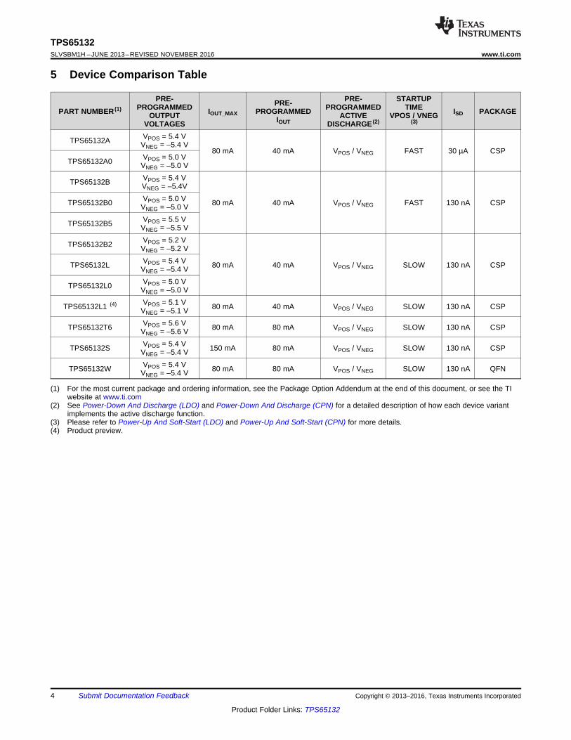
(1) For the most current package and ordering information, see the Package Option Addendum at the end of this document, or see the TIwebsite at www.ti.com
(2) See Power-Down And Discharge (LDO) and Power-Down And Discharge (CPN) for a detailed description of how each device variantimplements the active discharge function.
(3) Please refer to Power-Up And Soft-Start (LDO) and Power-Up And Soft-Start (CPN) for more details.(4) Product preview.
5 Device Comparison Table
PART NUMBER (1)PRE-
PROGRAMMEDOUTPUT
VOLTAGESIOUT_MAX
PRE-PROGRAMMED
IOUT
PRE-PROGRAMMED
ACTIVEDISCHARGE (2)
STARTUPTIME
VPOS / VNEG(3)
ISD PACKAGE
TPS65132A VPOS = 5.4 VVNEG = –5.4 V
80 mA 40 mA VPOS / VNEG FAST 30 µA CSPTPS65132A0 VPOS = 5.0 V
VNEG = –5.0 V
TPS65132B VPOS = 5.4 VVNEG = –5.4V
80 mA 40 mA VPOS / VNEG FAST 130 nA CSPTPS65132B0 VPOS = 5.0 VVNEG = –5.0 V
TPS65132B5 VPOS = 5.5 VVNEG = –5.5 V
TPS65132B2 VPOS = 5.2 VVNEG = –5.2 V
80 mA 40 mA VPOS / VNEG SLOW 130 nA CSPTPS65132L VPOS = 5.4 VVNEG = –5.4 V
TPS65132L0 VPOS = 5.0 VVNEG = –5.0 V
TPS65132L1 (4) VPOS = 5.1 VVNEG = –5.1 V 80 mA 40 mA VPOS / VNEG SLOW 130 nA CSP
TPS65132T6 VPOS = 5.6 VVNEG = –5.6 V 80 mA 80 mA VPOS / VNEG SLOW 130 nA CSP
TPS65132S VPOS = 5.4 VVNEG = –5.4 V 150 mA 80 mA VPOS / VNEG SLOW 130 nA CSP
TPS65132W VPOS = 5.4 VVNEG = –5.4 V 80 mA 80 mA VPOS / VNEG SLOW 130 nA QFN
(bottom view)TPS65132Ax / Bx / Lx / Tx
(bottom view)TPS65132Sx
(top view)TPS65132Ax / Bx / Lx / Tx
(top view)TPS65132Sx
A
A
A
A
1
1
1
1
2
2
2
2
3
3
3
3
B
B
B
B
C
C
C
C
D
D
D
D
E
E
E
E
SCL
SCL
SCL
SCL
CFLY1
CFLY1
CFLY1
CFLY1
SDA
SDA
SDA
SDA
REG
REG
REG
REG
OUTP
OUTP
OUTP
OUTP
AGND
AGND
AGND
AGND
REG
REG
REG
REG
OUTN
OUTN
OUTN
OUTN
CFLY2
CFLY2
CFLY2
CFLY2
PGND
PGND
PGND
PGND
ENP
EN
ENP
EN
VIN
VIN
VIN
VIN
SW
SW
SW
SW
PGND
PGND
PGND
PGND
ENN
SYNC
ENN
SYNC
5
TPS65132www.ti.com SLVSBM1H –JUNE 2013–REVISED NOVEMBER 2016
Product Folder Links: TPS65132
Submit Documentation FeedbackCopyright © 2013–2016, Texas Instruments Incorporated
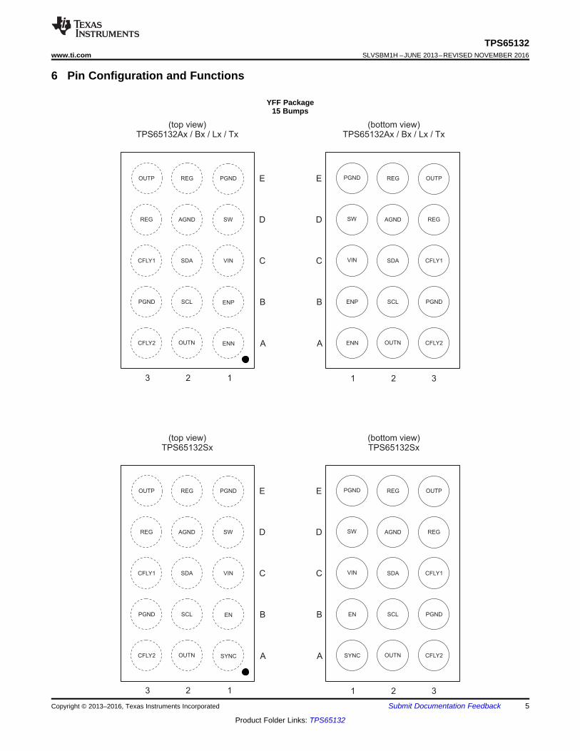
6 Pin Configuration and Functions
YFF Package15 Bumps
6
TPS65132SLVSBM1H –JUNE 2013–REVISED NOVEMBER 2016 www.ti.com
Product Folder Links: TPS65132
Submit Documentation Feedback Copyright © 2013–2016, Texas Instruments Incorporated
Pin FunctionsPIN
I/O DESCRIPTIONNAME Ax, Bx, Lx, Tx SxAGND D2 D2 — Analog groundCFLY1 C3 C3 I/O Negative charge pump flying capacitor pinCFLY2 A3 A3 I/O Negative charge pump flying capacitor pinEN — B1 Enable pin (sequence programmed)ENN A1 — I Enable pin for VNEG railENP B1 B1 I Enable pin for VPOS railOUTP E3 E3 O Output pin of the LDO (VPOS)OUTN A2 A2 O Output pin of the negative charge pump (VNEG)
PGNDB3 B3
— Power groundE1 E1
REGD3 D3
I/O Boost converter output pinE2 E2
SCL B2 B2 I/O I²C interface clock signal pinSDA C2 C2 I/O I²C interface data signal pinSW D1 D1 I/O Switch pin of the boost converterSYNC — A1 I Synchronization pin. 150 mA current enabled if this pin is pulled HIGH.VIN C1 C1 I Input voltage supply pin
PowerPAD
116
7
20
8
19
9
18
10
17
215
314
413
512
611
PGNDOUTP
SW
PGNDOUTP
SW
AGND
SD
A
REG
RE
G
VIN
SC
L
CFLY1
AG
ND
ENP
OU
TN
PGND
ENN
CF
LY
2
PGND
RVC package(bottom view)
RVC package(top view)
PowerPAD
1 16
7
20
8
19
9
18
10
17
2 15
3 14
4 13
5 12
6 11
PGND OUTP
SW
PGND OUTP
SW
AGND
SD
A
REG
RE
G
VIN
SC
L
CFLY1
AG
ND
ENP
OU
TN
PGND
ENN
CF
LY
2
PGND
7
TPS65132www.ti.com SLVSBM1H –JUNE 2013–REVISED NOVEMBER 2016
Product Folder Links: TPS65132
Submit Documentation FeedbackCopyright © 2013–2016, Texas Instruments Incorporated
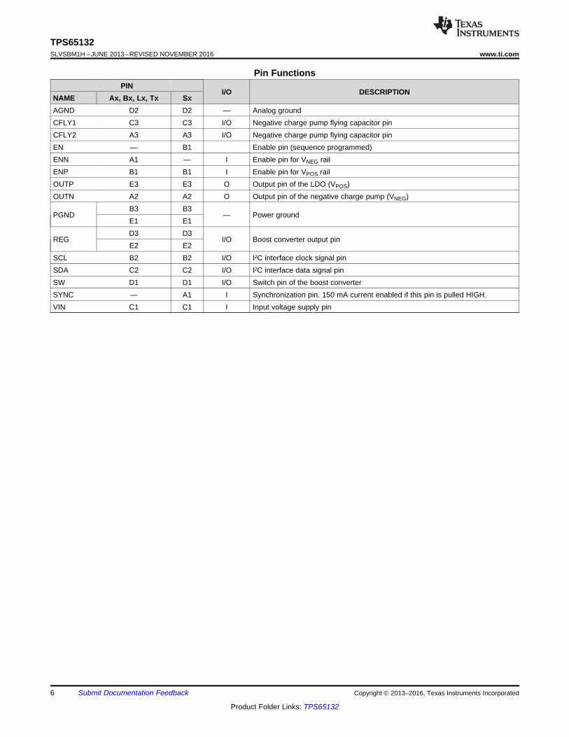
QFN Package20 Pins
Pin FunctionsPIN
I/O DESCRIPTIONNAME Wx
AGND3
— Analog ground17
CFLY1 13 I/O Negative charge pump flying capacitor pinCFLY2 10 I/O Negative charge pump flying capacitor pinENN 6 I Enable pin for VNEG railENP 5 I Enable pin for VPOS rail
OUTP16
O Output pin of the LDO (VPOS)15
OUTN 9 O Output pin of the negative charge pump (VNEG)
PGND
1
— Power ground2
1112
REG14
I/O Boost converter output pin18
SCL 8 I/O I²C interface clock signal pinSDA 7 I/O I²C interface data signal pin
SW19
I/O Switch pin of the boost converter20
VIN 4 I Input voltage supply pin
8
TPS65132SLVSBM1H –JUNE 2013–REVISED NOVEMBER 2016 www.ti.com
Product Folder Links: TPS65132
Submit Documentation Feedback Copyright © 2013–2016, Texas Instruments Incorporated
(1) Stresses beyond those listed under absolute maximum ratings may cause permanent damage to the device. These are stress ratingsonly, and functional operation of the device at these or any other conditions beyond those indicated under recommended operatingconditions is not implied. Exposure to absolute–maximum–rated conditions for extended periods may affect device reliability.
(2) All voltage values are with respect to ground.
7 Specifications
7.1 Absolute Maximum Ratings (1) (2)
over operating free-air temperature range (unless otherwise noted)VALUE
UNITMIN MAX
Voltage rangeCFLY1, EN, ENN, ENP, OUTP, REG, SCL, SDA, SW, SYNC,VIN –0.3 7 V
CFLY2, OUTN –7 0.3 VContinuous total power dissipation See Thermal InformationOperating junction temperature, TJ –40 150 °COperating ambient temperature, TA –40 85 °CStorage temperature, Tstg –65 150 °C
(1) JEDEC document JEP155 states that 500-V HBM allows safe manufacturing with a standard ESD control process.(2) JEDEC document JEP157 states that 250-V CDM allows safe manufacturing with a standard ESD control process.
7.2 ESD RatingsVALUE UNIT
VESD
Human body model (HBM), per ANSI/ESDA/JEDEC JS-001, all pins (1) ±2000 VCharged device model (CDM) per JEDEC specification JESD22-C101, all pins (2) ±500 V
(1) Please see Detailed Description section for further information.(2) X7R (or better dielectric material) is recommended.
7.3 Recommended Operating ConditionsMIN TYP MAX UNIT
VIN Input voltage range 2.5 5.5 VL Inductor (1) 2.2 4.7 µHCIN Input capacitor (1) (2) 4.7 µFCFLY Flying capacitor (1) (2) 2.2 µFCOUTP, COUTN, CREG Output capacitors (1) (2) 4.7 µFTA Operating ambient temperature –40 85 °CTJ Operating junction temperature –40 125 °C
(1) For more information about traditional and new thermal metrics, see the Semiconductor and IC Package Thermal Metrics applicationreport, SPRA953.
7.4 Thermal Information
THERMAL METRIC (1)
TPS65132 TPS65132UNITYFF RVC
(15) BALLS (20) PINSRθJA Junction-to-ambient thermal resistance 76.5 39.0 °C/WRθJCtop Junction-to-case (top) thermal resistance 0.2 42.7 °C/WRθJB Junction-to-board thermal resistance 44 13.6 °C/WψJT Junction-to-top characterization parameter 1.6 0.6 °C/WψJB Junction-to-board characterization parameter 43.4 13.6 °C/WRθJCbot Junction-to-case (bottom) thermal resistance N/A 3.8 °C/W
9
TPS65132www.ti.com SLVSBM1H –JUNE 2013–REVISED NOVEMBER 2016
Product Folder Links: TPS65132
Submit Documentation FeedbackCopyright © 2013–2016, Texas Instruments Incorporated
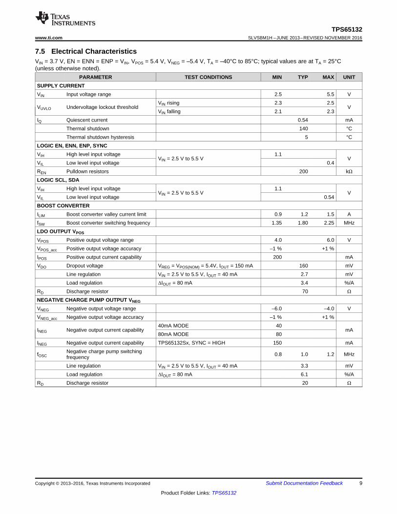
7.5 Electrical CharacteristicsVIN = 3.7 V, EN = ENN = ENP = VIN, VPOS = 5.4 V, VNEG = –5.4 V, TA = –40°C to 85°C; typical values are at TA = 25°C(unless otherwise noted).
PARAMETER TEST CONDITIONS MIN TYP MAX UNITSUPPLY CURRENTVIN Input voltage range 2.5 5.5 V
VUVLO Undervoltage lockout thresholdVIN rising 2.3 2.5
VVIN falling 2.1 2.3
IQ Quiescent current 0.54 mAThermal shutdown 140 °CThermal shutdown hysteresis 5 °C
LOGIC EN, ENN, ENP, SYNCVIH High level input voltage
VIN = 2.5 V to 5.5 V1.1
VVIL Low level input voltage 0.4REN Pulldown resistors 200 kΩLOGIC SCL, SDAVIH High level input voltage
VIN = 2.5 V to 5.5 V1.1
VVIL Low level input voltage 0.54BOOST CONVERTERILIM Boost converter valley current limit 0.9 1.2 1.5 AfSW Boost converter switching frequency 1.35 1.80 2.25 MHzLDO OUTPUT VPOS
VPOS Positive output voltage range 4.0 6.0 VVPOS_acc Positive output voltage accuracy –1 % +1 %IPOS Positive output current capability 200 mAVDO Dropout voltage VREG = VPOS(NOM) = 5.4V, IOUT = 150 mA 160 mV
Line regulation VIN = 2.5 V to 5.5 V, IOUT = 40 mA 2.7 mVLoad regulation ΔIOUT = 80 mA 3.4 %/A
RD Discharge resistor 70 Ω
NEGATIVE CHARGE PUMP OUTPUT VNEG
VNEG Negative output voltage range –6.0 –4.0 VVNEG_acc Negative output voltage accuracy –1 % +1 %
INEG Negative output current capability40mA MODE 40
mA80mA MODE 80
INEG Negative output current capability TPS65132Sx, SYNC = HIGH 150 mA
fOSCNegative charge pump switchingfrequency 0.8 1.0 1.2 MHz
Line regulation VIN = 2.5 V to 5.5 V, IOUT = 40 mA 3.3 mVLoad regulation ΔIOUT = 80 mA 6.1 %/A
RD Discharge resistor 20 Ω
tf tLOWtr
thd;STA
thd;DAT
tsu;DATtf
HIGH
tsu;STA
S Sr P S
thd;STAtr
tBUF
tsu;STO
SDA
SCL
10
TPS65132SLVSBM1H –JUNE 2013–REVISED NOVEMBER 2016 www.ti.com
Product Folder Links: TPS65132
Submit Documentation Feedback Copyright © 2013–2016, Texas Instruments Incorporated
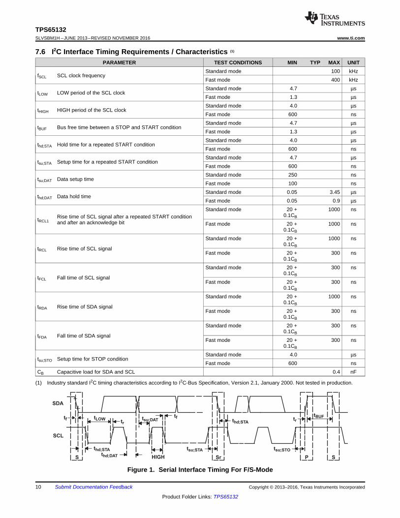
(1) Industry standard I2C timing characteristics according to I2C-Bus Specification, Version 2.1, January 2000. Not tested in production.
7.6 I2C Interface Timing Requirements / Characteristics (1)
PARAMETER TEST CONDITIONS MIN TYP MAX UNIT
fSCL SCL clock frequencyStandard mode 100 kHzFast mode 400 kHz
tLOW LOW period of the SCL clockStandard mode 4.7 µsFast mode 1.3 µs
tHIGH HIGH period of the SCL clockStandard mode 4.0 µsFast mode 600 ns
tBUF Bus free time between a STOP and START conditionStandard mode 4.7 µsFast mode 1.3 µs
thd;STA Hold time for a repeated START conditionStandard mode 4.0 µsFast mode 600 ns
tsu;STA Setup time for a repeated START conditionStandard mode 4.7 µsFast mode 600 ns
tsu;DAT Data setup timeStandard mode 250 nsFast mode 100 ns
thd;DAT Data hold timeStandard mode 0.05 3.45 µsFast mode 0.05 0.9 µs
tRCL1Rise time of SCL signal after a repeated START conditionand after an acknowledge bit
Standard mode 20 +0.1CB
1000 ns
Fast mode 20 +0.1CB
1000 ns
tRCL Rise time of SCL signal
Standard mode 20 +0.1CB
1000 ns
Fast mode 20 +0.1CB
300 ns
tFCL Fall time of SCL signal
Standard mode 20 +0.1CB
300 ns
Fast mode 20 +0.1CB
300 ns
tRDA Rise time of SDA signal
Standard mode 20 +0.1CB
1000 ns
Fast mode 20 +0.1CB
300 ns
tFDA Fall time of SDA signal
Standard mode 20 +0.1CB
300 ns
Fast mode 20 +0.1CB
300 ns
tsu;STO Setup time for STOP conditionStandard mode 4.0 µsFast mode 600 ns
CB Capacitive load for SDA and SCL 0.4 nF
Figure 1. Serial Interface Timing For F/S-Mode
0.8
0.85
0.9
0.95
1
1.05
1.1
1.15
1.2
-40 10 60
Fos
c (
MH
z)
Ta (�C)
VIN = 2.9 V
VIN = 3.7 V
VIN = 4.5 V
C03
2.2
2.25
2.3
2.35
2.4
2.45
2.5
-40 -20 0 20 40 60 80
VIN
(V
)
Ta (�C)
UVLO_rising
UVLO_falling
C03
0.4
0.42
0.44
0.46
0.48
0.5
0.52
0.54
0.56
0.58
0.6
-40 -20 0 20 40 60 80
Iq (
mA
)
Ta (�C)
VIN = 2.9 V
VIN = 3.7 V
VIN = 4.5 V
C04
0
0.5
1
1.5
2
2.5
3
-40 -20 0 20 40 60 80
Isd
(µA
)
Ta (�C)
VIN = 2.9 V
VIN = 3.7 V
VIN = 4.5 V
C04
11
TPS65132www.ti.com SLVSBM1H –JUNE 2013–REVISED NOVEMBER 2016
Product Folder Links: TPS65132
Submit Documentation FeedbackCopyright © 2013–2016, Texas Instruments Incorporated
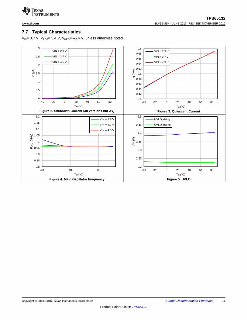
7.7 Typical CharacteristicsVIN= 3.7 V, VPOS= 5.4 V, VNEG= –5.4 V, unless otherwise noted
Figure 2. Shutdown Current (all versions but Ax) Figure 3. Quiescent Current
Figure 4. Main Oscillator Frequency Figure 5. UVLO
LDO
CPN
VIN
(battery voltage)
VPOS
VNEG
5.4 V/40 mA
–5.4 V/40 mA
SYNCBOOST
ENP
VIN
SW REG
OUTP
OUTN
ENN
SCL
AGNDPG
ND
CF
LY
1
CF
LY
2
SDA
12
TPS65132SLVSBM1H –JUNE 2013–REVISED NOVEMBER 2016 www.ti.com
Product Folder Links: TPS65132
Submit Documentation Feedback Copyright © 2013–2016, Texas Instruments Incorporated
8 Detailed Description
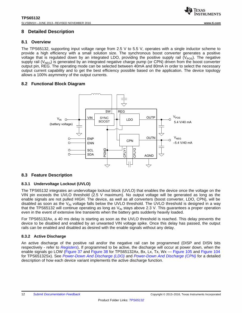
8.1 OverviewThe TPS65132, supporting input voltage range from 2.5 V to 5.5 V, operates with a single inductor scheme toprovide a high efficiency with a small solution size. The synchronous boost converter generates a positivevoltage that is regulated down by an integrated LDO, providing the positive supply rail (VPOS). The negativesupply rail (VNEG) is generated by an integrated negative charge pump (or CPN) driven from the boost converteroutput pin, REG. The operating mode can be selected between 40mA and 80mA in order to select the necessaryoutput current capability and to get the best efficiency possible based on the application. The device topologyallows a 100% asymmetry of the output currents.
8.2 Functional Block Diagram
8.3 Feature Description
8.3.1 Undervoltage Lockout (UVLO)The TPS65132 integrates an undervoltage lockout block (UVLO) that enables the device once the voltage on theVIN pin exceeds the UVLO threshold (2.5 V maximum). No output voltage will be generated as long as theenable signals are not pulled HIGH. The device, as well as all converters (boost converter, LDO, CPN), will bedisabled as soon as the VIN voltage falls below the UVLO threshold. The UVLO threshold is designed in a waythat the TPS65132 will continue operating as long as VIN stays above 2.3 V. This guarantees a proper operationeven in the event of extensive line transients when the battery gets suddenly heavily loaded.
For TPS65132Ax, a 40 ms delay is starting as soon as the UVLO threshold is reached. This delay prevents thedevice to be disabled and enabled by an unwanted VIN voltage spike. Once this delay has passed, the outputrails can be enabled and disabled as desired with the enable signals without any delay.
8.3.2 Active DischargeAn active discharge of the positive rail and/or the negative rail can be programmed (DISP and DISN bitsrespectively - refer to Registers). If programmed to be active, the discharge will occur at power down, when theenable signals go LOW (Figure 37 and Figure 38 for TPS65132Ax, Bx, Lx, Tx, Wx — Figure 105 and Figure 104for TPS65132Sx). See Power-Down And Discharge (LDO) and Power-Down And Discharge (CPN) for a detaileddescription of how each device variant implements the active discharge function.
13
TPS65132www.ti.com SLVSBM1H –JUNE 2013–REVISED NOVEMBER 2016
Product Folder Links: TPS65132
Submit Documentation FeedbackCopyright © 2013–2016, Texas Instruments Incorporated
Feature Description (continued)8.3.3 Boost Converter
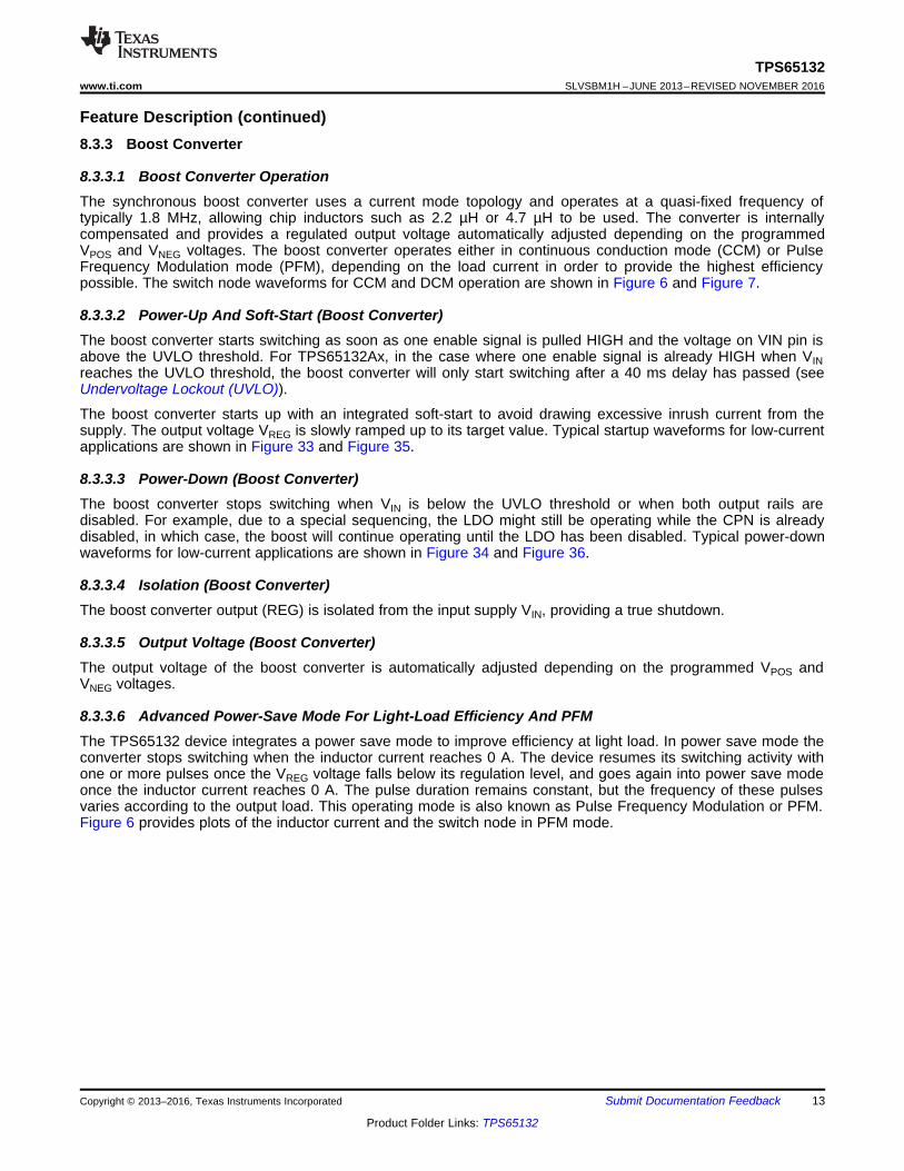
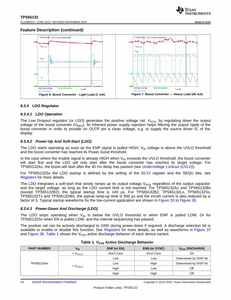
8.3.3.1 Boost Converter OperationThe synchronous boost converter uses a current mode topology and operates at a quasi-fixed frequency oftypically 1.8 MHz, allowing chip inductors such as 2.2 µH or 4.7 µH to be used. The converter is internallycompensated and provides a regulated output voltage automatically adjusted depending on the programmedVPOS and VNEG voltages. The boost converter operates either in continuous conduction mode (CCM) or PulseFrequency Modulation mode (PFM), depending on the load current in order to provide the highest efficiencypossible. The switch node waveforms for CCM and DCM operation are shown in Figure 6 and Figure 7.
8.3.3.2 Power-Up And Soft-Start (Boost Converter)The boost converter starts switching as soon as one enable signal is pulled HIGH and the voltage on VIN pin isabove the UVLO threshold. For TPS65132Ax, in the case where one enable signal is already HIGH when VINreaches the UVLO threshold, the boost converter will only start switching after a 40 ms delay has passed (seeUndervoltage Lockout (UVLO)).
The boost converter starts up with an integrated soft-start to avoid drawing excessive inrush current from thesupply. The output voltage VREG is slowly ramped up to its target value. Typical startup waveforms for low-currentapplications are shown in Figure 33 and Figure 35.
8.3.3.3 Power-Down (Boost Converter)The boost converter stops switching when VIN is below the UVLO threshold or when both output rails aredisabled. For example, due to a special sequencing, the LDO might still be operating while the CPN is alreadydisabled, in which case, the boost will continue operating until the LDO has been disabled. Typical power-downwaveforms for low-current applications are shown in Figure 34 and Figure 36.
8.3.3.4 Isolation (Boost Converter)The boost converter output (REG) is isolated from the input supply VIN, providing a true shutdown.
8.3.3.5 Output Voltage (Boost Converter)The output voltage of the boost converter is automatically adjusted depending on the programmed VPOS andVNEG voltages.
8.3.3.6 Advanced Power-Save Mode For Light-Load Efficiency And PFMThe TPS65132 device integrates a power save mode to improve efficiency at light load. In power save mode theconverter stops switching when the inductor current reaches 0 A. The device resumes its switching activity withone or more pulses once the VREG voltage falls below its regulation level, and goes again into power save modeonce the inductor current reaches 0 A. The pulse duration remains constant, but the frequency of these pulsesvaries according to the output load. This operating mode is also known as Pulse Frequency Modulation or PFM.Figure 6 provides plots of the inductor current and the switch node in PFM mode.
2
3
4
VSW
1 µs/div
VREG_AC
IL
Ch2 50.0 mV/div
Ch3 2.00 V/div
Ch4 100 mA/div
TPS65132B - Low-Current Application
2
Ch2 50.0 mV/div
3
Ch3 2.00 V/div
4Ch4 100 mA/div
VSW
1 µs/div
VREG_AC
IL
TPS65132B - Low-Current Application
14
TPS65132SLVSBM1H –JUNE 2013–REVISED NOVEMBER 2016 www.ti.com
Product Folder Links: TPS65132
Submit Documentation Feedback Copyright © 2013–2016, Texas Instruments Incorporated
Feature Description (continued)
Figure 6. Boost Converter - Light Load (1 mA) Figure 7. Boost Converter — Heavy Load (40 mA)
8.3.4 LDO Regulator
8.3.4.1 LDO OperationThe Low Dropout regulator (or LDO) generates the positive voltage rail, VPOS, by regulating down the outputvoltage of the boost converter (VREG). Its inherent power supply rejection helps filtering the output ripple of theboost converter in order to provide on OUTP pin a clean voltage, e.g. to supply the source driver IC of thedisplay.
8.3.4.2 Power-Up And Soft-Start (LDO)The LDO starts operating as soon as the ENP signal is pulled HIGH, VIN voltage is above the UVLO thresholdand the boost converter has reached its Power Good threshold.
In the case where the enable signal is already HIGH when VIN exceeds the UVLO threshold, the boost converterwill start first and the LDO will only start after the boost converter has reached its target voltage. ForTPS65132Ax, the boost will start after the 40 ms delay has passed (see Undervoltage Lockout (UVLO)).
For TPS65132Sx the LDO startup is defined by the setting of the DLYx register and the SEQU bits, seeRegisters for more details.
The LDO integrates a soft-start that slowly ramps up its output voltage VPOS regardless of the output capacitorand the target voltage, as long as the LDO current limit is not reached. For TPS65132Ax and TPS65132Bx(except TPS65132B2), the typical startup time is 140 µs. For TPS65132B2, TPS65132Lx, TPS65132Sx,TPS65132Tx and TPS65132Wx, the typical ramp-up time is 500 µs and the inrush current is also reduced by afactor of 3. Typical startup waveforms for the low-current application are shown in Figure 33 to Figure 35.
8.3.4.3 Power-Down And Discharge (LDO)The LDO stops operating when VIN is below the UVLO threshold or when ENP is pulled LOW. Or forTPS65132Sx when EN is pulled LOW, and the internal sequencing has passed.
The positive rail can be actively discharged to GND during power-down if required. A discharge selection bit isavailable to enable or disable this function. See Registers for more details, as well as waveforms in Figure 37and Figure 38. Table 1 shows the VPOS active discharge behavior of each device variant.
Table 1. VPOS Active Discharge BehaviorPART NUMBER VIN ENP (or EN) ENN (or SYNC) VPOS DISCHARGE
TPS65132Ax
< VUVLO Don't Care Don't Care On
> VUVLO
Low Low Determined by DISP bitLow High Determined by DISP bitHigh Low OffHigh High Off
´OUT NEGSTARTUP
STARTUP
C Vt =
I
15
TPS65132www.ti.com SLVSBM1H –JUNE 2013–REVISED NOVEMBER 2016
Product Folder Links: TPS65132
Submit Documentation FeedbackCopyright © 2013–2016, Texas Instruments Incorporated
Feature Description (continued)Table 1. VPOS Active Discharge Behavior (continued)
PART NUMBER VIN ENP (or EN) ENN (or SYNC) VPOS DISCHARGE
TPS65132BxTPS65132LxTPS65132SxTPS65132TxTPS65132Wx
< VUVLO Don't Care Don't Care On
> VUVLO
Low Low OnLow High Determined by DISP bitHigh Low OffHigh High Off
8.3.4.4 Isolation (LDO)The LDO is isolating the VPOS rail from VREG (boost converter output) as long as the rail is not enabled in order toensure flexible startup like VNEG before VPOS.
8.3.4.5 Setting The Output Voltage (LDO)The output voltage of the LDO is programmable via a I2C compatible interface, from –6.0 V to –4.0 V in 100 mVsteps. For more details, please refer to the VPOS Register – Address: 0x00
8.3.5 Negative Charge Pump
8.3.5.1 OperationThe negative charge pump (CPN) generates the negative voltage rail, VNEG, by inverting and regulating theoutput voltage of the boost converter (VREG). The charge pump uses 4 switches and an external flying capacitorto generate the negative rail. Two of the switches are turned on in the first phase to charge the flying capacitorup to VREG, and in the second phase they are turned-off and the two others turn on to pump the energynegatively out of the OUTN capacitor.
8.3.5.2 Power-Up And Soft-Start (CPN)The CPN starts operating as soon as the ENN signal is pulled HIGH, VIN voltage is above the UVLO thresholdand the boost converter has reached its Power Good threshold.
In the case where the enable signal is already HIGH when VIN reaches the UVLO threshold, the boost converterwill start first and the CPN will only start after the boost converter has reached its target voltage. ForTPS65132Ax, the boost will start after the 40 ms delay has passed (see Undervoltage Lockout (UVLO)).
For TPS65132Sx the CPN startup is defined by the setting of the DLYx register and the SEQU bits, seeRegisters for more details.
The CPN integrates a soft-start that slowly ramps up its output voltage VNEG within a time defined by the selectedmode (40mA or 80mA), the output voltage and the output capacitor value. For TPS65132Ax and TPS65132Bx(except TPS65132B2), the startup current charging the output capacitor in 40mA mode is 50 mA, and 100 mAtypically in 80mA mode. For TPS65132B2, TPS65132Lx, TPS65132Tx, and TPS65132Wx, the typical ramp-uptimes are slowed down by a factor of 4 (i.e 12.5 mA and 25 mA typical output current for 40mA and 80mA modesrespectively) and the inrush current is also reduced by a factor of about 4. Typical startup waveforms for the low-current application are shown in Figure 39 to Figure 42.
For TPS65132Sx, the negative rail starts-up in 40mA or 80mA mode, thus the startup current is set by the modethe device is programmed to, and not related to the SYNC pin state. The full current of 150 mA minimum is onlyreleased once both rails (VPOS and VNEG) have reached their Power Good levels.
The estimated startup time can be calculated using the following formula:
Where:tSTARTUP = startup time of the VNEG railCOUT = output capacitance of the VNEG railVNEG = target output voltage
16
TPS65132SLVSBM1H –JUNE 2013–REVISED NOVEMBER 2016 www.ti.com
Product Folder Links: TPS65132
Submit Documentation Feedback Copyright © 2013–2016, Texas Instruments Incorporated
ISTARTUP = output current of the VNEG rail charging up the output capacitor at startup (12.5 mA, 25 mA, 50 mAor 100 mA as described above)
8.3.5.3 Power-Down And Discharge (CPN)The CPN stops operating when VIN is below the UVLO threshold or when ENN is pulled LOW.
Or when EN is pulled LOW in the TPS65132Sx, and the internal sequencing has passed.
The negative rail can be actively discharged to GND during power-down if required. A discharge selection bit isavailable to enable or disable this function. See for more details, as well as waveforms Figure 37 and Figure 38.Table 2 shows the VNEG discharge behavior of each device variant.
Table 2. VNEG Active Discharge BehaviorPART NUMBER VIN ENP (or EN) ENN (or SYNC) VNEG DISCHARGE
TPS65132Ax
< VUVLO Don't Care Don't Care On
> VUVLO
Low Low Determined by DISN bitLow High OffHigh Low Determined by DISN bitHigh High Off
TPS65132BxTPS65132LxTPS65132TxTPS65132Wx
< VUVLO Don't Care Don't Care On
> VUVLO
Low Low OnLow High OffHigh Low Determined by DISN bitHigh High Off
TPS65132Sx
< VUVLO Don't Care Don't Care On
> VUVLO
Low Low OnLow High Determined by DISN bitHigh Low OffHigh High Off
8.3.5.4 Isolation (CPN)The CPN isolates the VNEG rail from VREG (boost converter output) as long as the rail is not enabled in order toensure flexible startup like VPOS before VNEG.
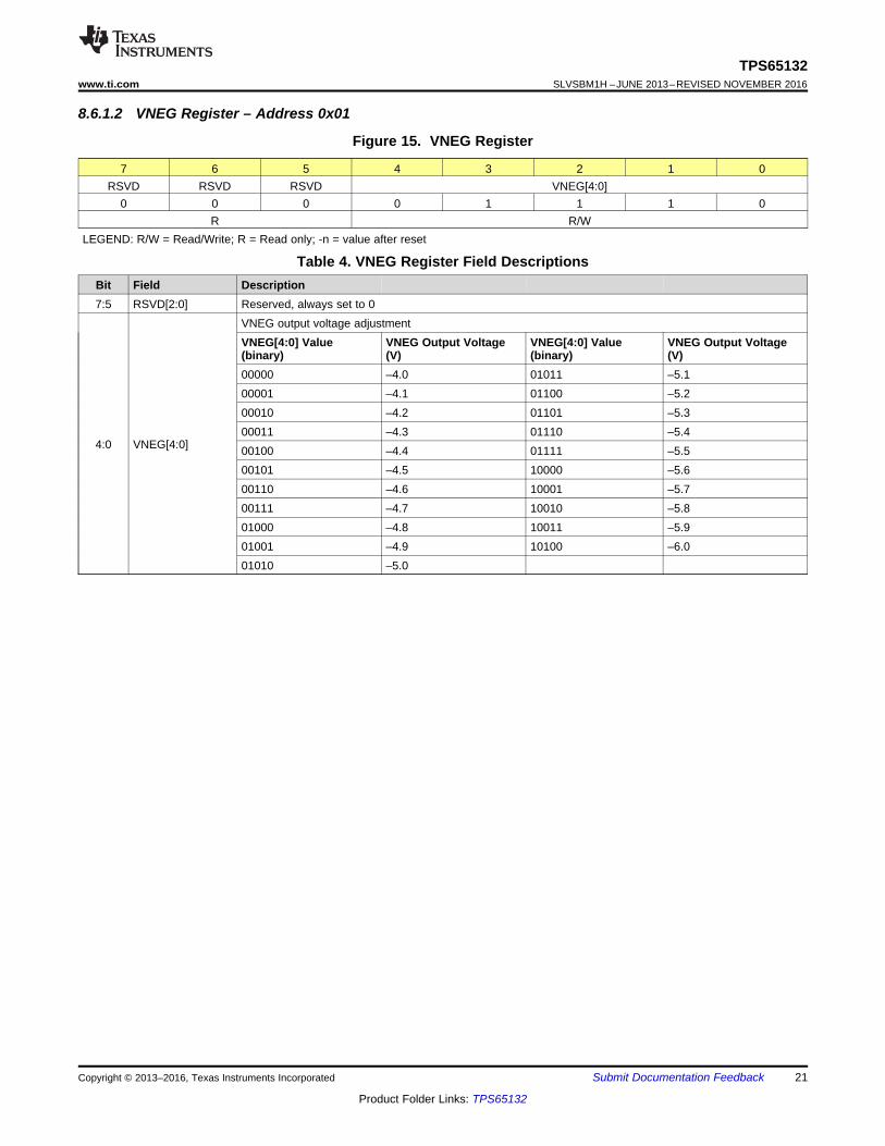
8.3.5.5 Setting The Output Voltage (CPN)The output voltage of the CPN is programmable via a I2C compatible interface, from –4.0 V to –6.0 V in 100 mVsteps. For more details, please refer to the VNEG Register – Address 0x01.
8.4 Device Functional Modes
8.4.1 Enabling and Disabling the DeviceAt startup (VIN goes above UVLO and at least one of the enable pins (ENP, ENN, or EN) goes HIGH), theEEPROM content is loaded into the DAC registers and the IC starts with these default values. The TPS65132 isenabled as long as the VIN voltage is above the UVLO and one of the enable pins (ENP, ENN, or EN) is HIGH.
Pulling ENP or ENN LOW disables either rail (VPOS or VNEG respectively); and, pulling both pins LOW disablesthe device entirely (the internal oscillator of the TPS65132Ax continues running to allow access to the I²Cinterface).
For TPS65132Sx, pulling EN LOW disables the device.
Slave Address R/W AA PS
1 7 1 1 1 18
“0” Write
8
A
1
From Master to Slave
From Slave to Master
AA
=
=
Acknowledge (SDA LOW)
Not Acknowledge (SDA HIGH)
S = START condition
Sr = REPEATED START condition
P = STOP condition
Register Address Data Register
17
TPS65132www.ti.com SLVSBM1H –JUNE 2013–REVISED NOVEMBER 2016
Product Folder Links: TPS65132
Submit Documentation FeedbackCopyright © 2013–2016, Texas Instruments Incorporated
8.5 Programming
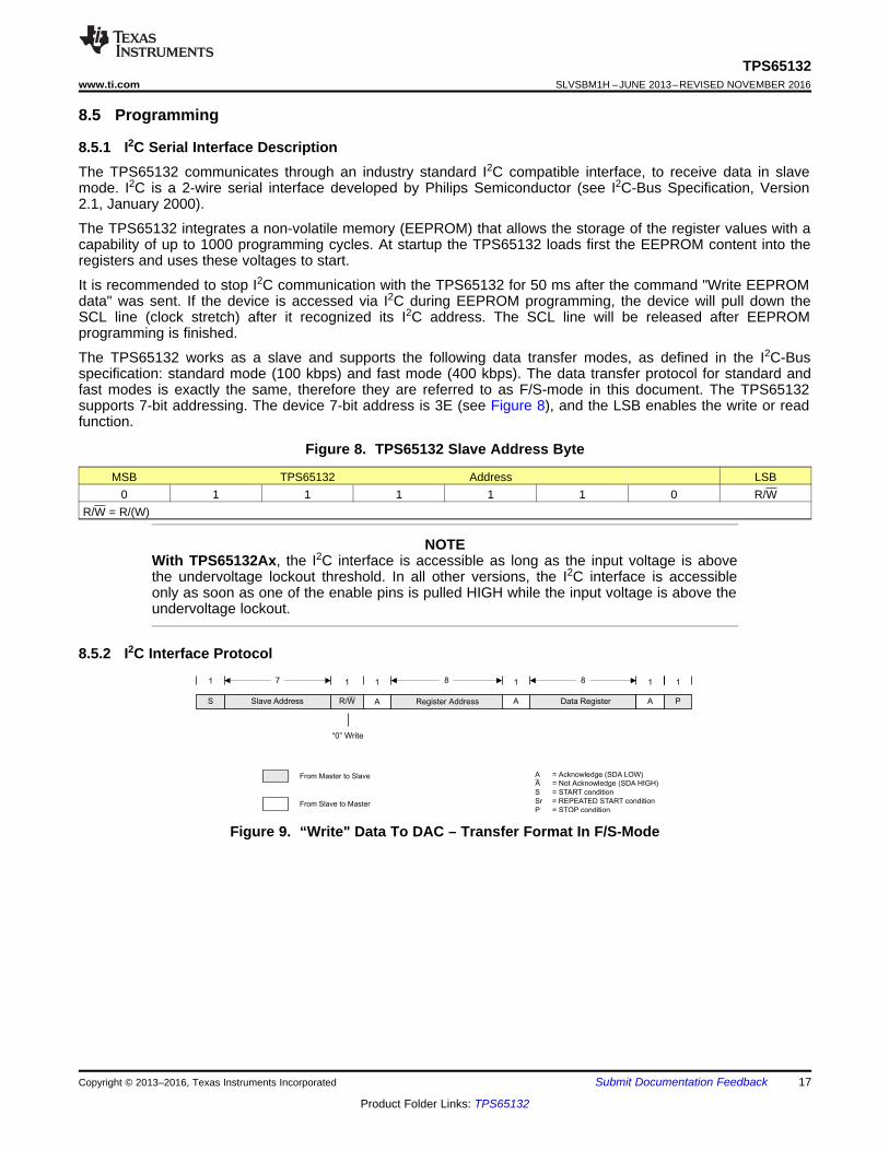
8.5.1 I2C Serial Interface DescriptionThe TPS65132 communicates through an industry standard I2C compatible interface, to receive data in slavemode. I2C is a 2-wire serial interface developed by Philips Semiconductor (see I2C-Bus Specification, Version2.1, January 2000).
The TPS65132 integrates a non-volatile memory (EEPROM) that allows the storage of the register values with acapability of up to 1000 programming cycles. At startup the TPS65132 loads first the EEPROM content into theregisters and uses these voltages to start.
It is recommended to stop I2C communication with the TPS65132 for 50 ms after the command "Write EEPROMdata" was sent. If the device is accessed via I2C during EEPROM programming, the device will pull down theSCL line (clock stretch) after it recognized its I2C address. The SCL line will be released after EEPROMprogramming is finished.
The TPS65132 works as a slave and supports the following data transfer modes, as defined in the I2C-Busspecification: standard mode (100 kbps) and fast mode (400 kbps). The data transfer protocol for standard andfast modes is exactly the same, therefore they are referred to as F/S-mode in this document. The TPS65132supports 7-bit addressing. The device 7-bit address is 3E (see Figure 8), and the LSB enables the write or readfunction.
Figure 8. TPS65132 Slave Address Byte
MSB TPS65132 Address LSB0 1 1 1 1 1 0 R/W
R/W = R/(W)
NOTEWith TPS65132Ax, the I2C interface is accessible as long as the input voltage is abovethe undervoltage lockout threshold. In all other versions, the I2C interface is accessibleonly as soon as one of the enable pins is pulled HIGH while the input voltage is above theundervoltage lockout.
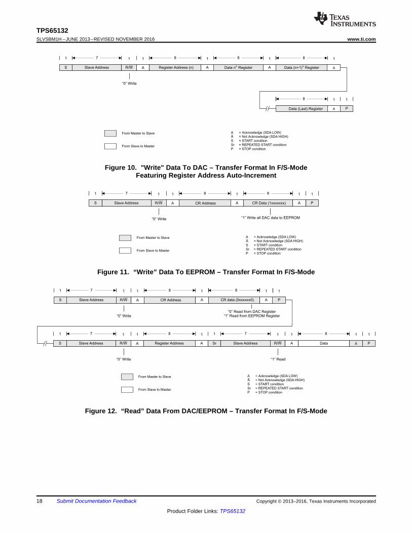
8.5.2 I2C Interface Protocol
Figure 9. “Write" Data To DAC – Transfer Format In F/S-Mode
Slave Address R/W CR Address AA PS
1 7 1 1 1 18 8
“0” Write
CR data (0xxxxxx0)
““1” Read from EEPROM Register
0” Read from DAC Register
A
1
From Master to Slave
From Slave to Master
AA
=
=
Acknowledge (SDA LOW)
Not Acknowledge (SDA HIGH)
S = START condition
Sr = REPEATED START condition
P = STOP condition
Slave Address R/W Register Address AA Data PS
1 7 1 1 1 1 18 8
“0” Write
Sr
1
Slave Address R/W
7 1
“1” Read
A
1
A
Slave Address R/W AA PS
1 7 1 1 1 18
“0” Write “1” Write all DAC data to EEPROM
8
A
1
From Master to Slave
From Slave to Master
AA
=
=
Acknowledge (SDA LOW)
Not Acknowledge (SDA HIGH)
S = START condition
Sr = REPEATED START condition
P = STOP condition
CR Address CR Data (1xxxxxxx)
Slave Address R/W Register Address (n) AA Data n Registerth
Data (Last) Register
Data (n+1) Registerth
P
S
1 7 1 1 1 1
1 1
8 8
8
“0” Write
8
A
1
From Master to Slave
From Slave to Master
AA
=
=
Acknowledge (SDA LOW)
Not Acknowledge (SDA HIGH)
S = START condition
Sr = REPEATED START condition
P = STOP condition
A
A
18
TPS65132SLVSBM1H –JUNE 2013–REVISED NOVEMBER 2016 www.ti.com
Product Folder Links: TPS65132
Submit Documentation Feedback Copyright © 2013–2016, Texas Instruments Incorporated
Figure 10. "Write" Data To DAC – Transfer Format In F/S-ModeFeaturing Register Address Auto-Increment
Figure 11. “Write” Data To EEPROM – Transfer Format In F/S-Mode
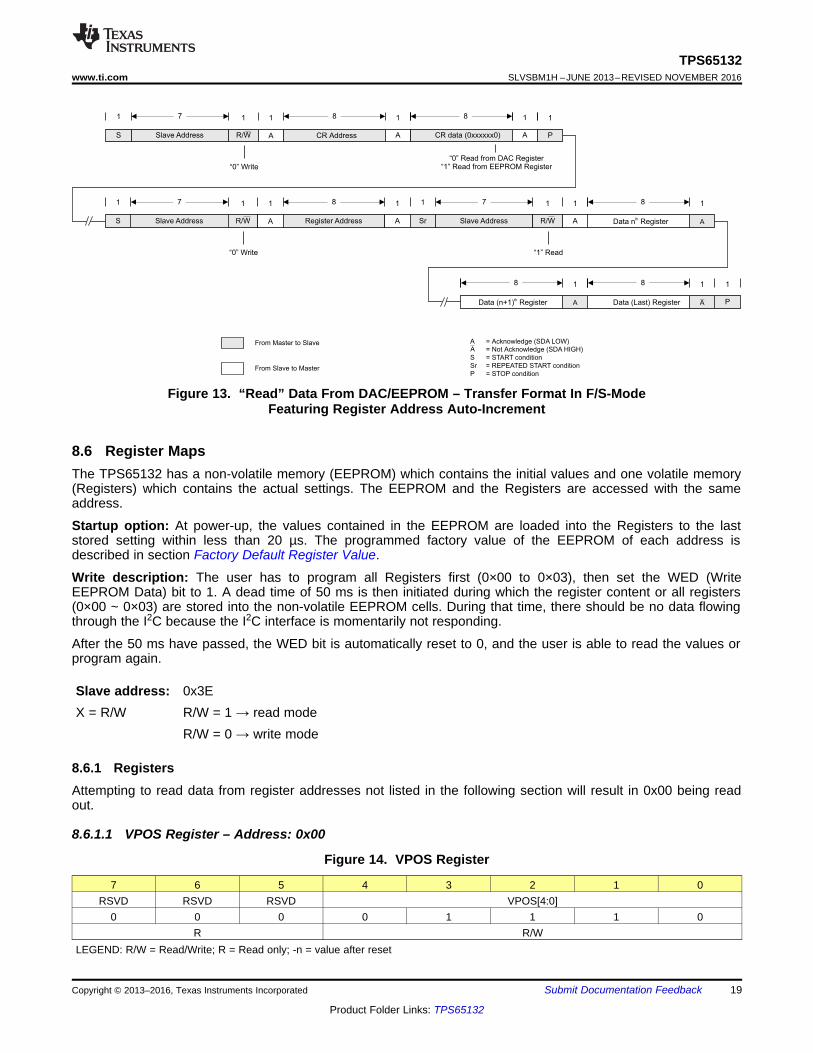
Figure 12. “Read” Data From DAC/EEPROM – Transfer Format In F/S-Mode
Data n Registerth
Data (Last) RegisterData (n+1) Registerth P
1
11 1
8
88
From Master to Slave
From Slave to Master
AA
=
=
Acknowledge (SDA LOW)
Not Acknowledge (SDA HIGH)
S = START condition
Sr = REPEATED START condition
P = STOP condition
A
AA
Slave Address R/W CR Address AA PS
1 7 1 1 1 18 8
“0” Write
CR data (0xxxxxx0)
““1” Read from EEPROM Register
0” Read from DAC Register
A
1
Slave Address R/W Register Address AAS
1 7 1 1 18
“0” Write
Sr
1
Slave Address R/W
7 1
“1” Read
A
1
19
TPS65132www.ti.com SLVSBM1H –JUNE 2013–REVISED NOVEMBER 2016
Product Folder Links: TPS65132
Submit Documentation FeedbackCopyright © 2013–2016, Texas Instruments Incorporated
Figure 13. “Read” Data From DAC/EEPROM – Transfer Format In F/S-ModeFeaturing Register Address Auto-Increment
8.6 Register MapsThe TPS65132 has a non-volatile memory (EEPROM) which contains the initial values and one volatile memory(Registers) which contains the actual settings. The EEPROM and the Registers are accessed with the sameaddress.
Startup option: At power-up, the values contained in the EEPROM are loaded into the Registers to the laststored setting within less than 20 µs. The programmed factory value of the EEPROM of each address isdescribed in section Factory Default Register Value.
Write description: The user has to program all Registers first (0×00 to 0×03), then set the WED (WriteEEPROM Data) bit to 1. A dead time of 50 ms is then initiated during which the register content or all registers(0×00 ~ 0×03) are stored into the non-volatile EEPROM cells. During that time, there should be no data flowingthrough the I2C because the I2C interface is momentarily not responding.
After the 50 ms have passed, the WED bit is automatically reset to 0, and the user is able to read the values orprogram again.
Slave address: 0x3EX = R/W R/W = 1 → read mode
R/W = 0 → write mode
8.6.1 RegistersAttempting to read data from register addresses not listed in the following section will result in 0x00 being readout.
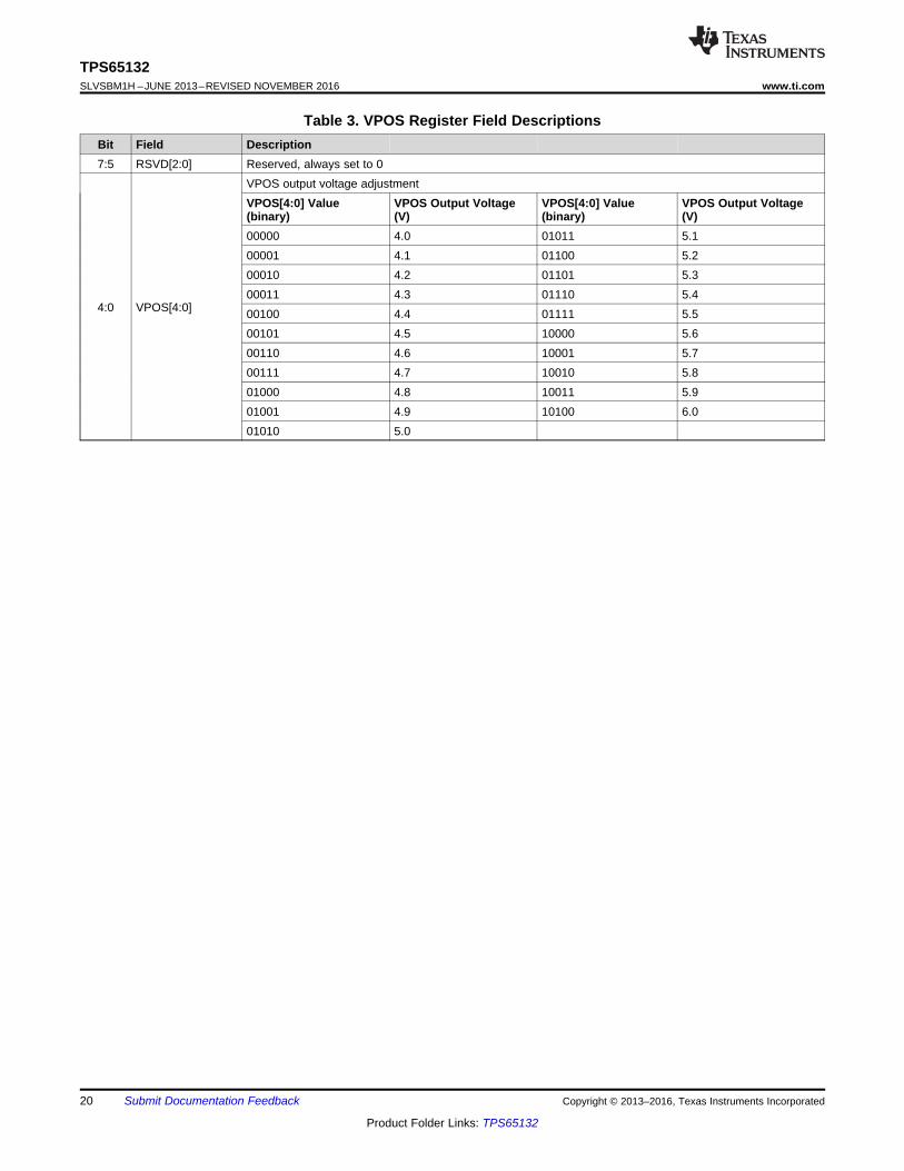
8.6.1.1 VPOS Register – Address: 0x00
Figure 14. VPOS Register
7 6 5 4 3 2 1 0RSVD RSVD RSVD VPOS[4:0]
0 0 0 0 1 1 1 0R R/W
LEGEND: R/W = Read/Write; R = Read only; -n = value after reset
20
TPS65132SLVSBM1H –JUNE 2013–REVISED NOVEMBER 2016 www.ti.com
Product Folder Links: TPS65132
Submit Documentation Feedback Copyright © 2013–2016, Texas Instruments Incorporated
Table 3. VPOS Register Field DescriptionsBit Field Description7:5 RSVD[2:0] Reserved, always set to 0
4:0 VPOS[4:0]
VPOS output voltage adjustmentVPOS[4:0] Value(binary)
VPOS Output Voltage(V)
VPOS[4:0] Value(binary)
VPOS Output Voltage(V)
00000 4.0 01011 5.100001 4.1 01100 5.200010 4.2 01101 5.300011 4.3 01110 5.400100 4.4 01111 5.500101 4.5 10000 5.600110 4.6 10001 5.700111 4.7 10010 5.801000 4.8 10011 5.901001 4.9 10100 6.001010 5.0
21
TPS65132www.ti.com SLVSBM1H –JUNE 2013–REVISED NOVEMBER 2016
Product Folder Links: TPS65132
Submit Documentation FeedbackCopyright © 2013–2016, Texas Instruments Incorporated
8.6.1.2 VNEG Register – Address 0x01
Figure 15. VNEG Register
7 6 5 4 3 2 1 0RSVD RSVD RSVD VNEG[4:0]
0 0 0 0 1 1 1 0R R/W
LEGEND: R/W = Read/Write; R = Read only; -n = value after reset
Table 4. VNEG Register Field DescriptionsBit Field Description7:5 RSVD[2:0] Reserved, always set to 0
4:0 VNEG[4:0]
VNEG output voltage adjustmentVNEG[4:0] Value(binary)
VNEG Output Voltage(V)
VNEG[4:0] Value(binary)
VNEG Output Voltage(V)
00000 –4.0 01011 –5.100001 –4.1 01100 –5.200010 –4.2 01101 –5.300011 –4.3 01110 –5.400100 –4.4 01111 –5.500101 –4.5 10000 –5.600110 –4.6 10001 –5.700111 –4.7 10010 –5.801000 –4.8 10011 –5.901001 –4.9 10100 –6.001010 –5.0
22
TPS65132SLVSBM1H –JUNE 2013–REVISED NOVEMBER 2016 www.ti.com
Product Folder Links: TPS65132
Submit Documentation Feedback Copyright © 2013–2016, Texas Instruments Incorporated
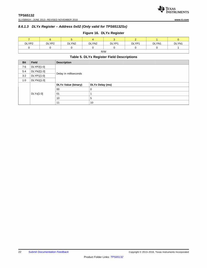
8.6.1.3 DLYx Register – Address 0x02 (Only valid for TPS65132Sx)
Figure 16. DLYx Register
7 6 5 4 3 2 1 0DLYP2 DLYP2 DLYN2 DLYN2 DLYP1 DLYP1 DLYN1 DLYN1
0 0 0 0 0 0 0 1R/W
Table 5. DLYx Register Field DescriptionsBit Field Description7:6 DLYP2[1:0]
Delay in milliseconds5:4 DLYN2[1:0]3:2 DLYP1[1:0]1:0 DLYN1[1:0]
DLYx[1:0]
DLYx Value (binary) DLYx Delay (ms)00 001 110 511 10
23
TPS65132www.ti.com SLVSBM1H –JUNE 2013–REVISED NOVEMBER 2016
Product Folder Links: TPS65132
Submit Documentation FeedbackCopyright © 2013–2016, Texas Instruments Incorporated
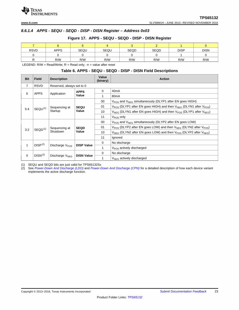
8.6.1.4 APPS - SEQU - SEQD - DISP - DISN Register – Address 0x03
Figure 17. APPS - SEQU - SEQD - DISP - DISN Register
7 6 5 4 3 2 1 0RSVD APPS SEQU SEQU SEQD SEQD DISP DISN
0 0 0 0 0 0 1 0R R/W R/W R/W R/W R/W R/W R/W
LEGEND: R/W = Read/Write; R = Read only; -n = value after reset
(1) SEQU and SEQD bits are just valid for TPS65132Sx(2) See Power-Down And Discharge (LDO) and Power-Down And Discharge (CPN) for a detailed description of how each device variant
implements the active discharge function.
Table 6. APPS - SEQU - SEQD - DISP - DISN Field Descriptions
Bit Field Description Value(binary) Action
7 RSVD Reserved, always set to 0
6 APPS Application APPSValue
0 40mA1 80mA
5:4 SEQU (1) Sequencing atStartup
SEQUValue
00 VPOS and VNEG simultaneously (DLYP1 after EN goes HIGH)01 VPOS (DLYP1 after EN goes HIGH) and then VNEG (DLYN1 after VPOS)10 VNEG (DLYN1 after EN goes HIGH) and then VPOS (DLYP1 after VNEG)11 VPOS only
3:2 SEQD (1) Sequencing atShutdown
SEQDValue
00 VPOS and VNEG simultaneously (DLYP2 after EN goes LOW)01 VPOS (DLYP2 after EN goes LOW) and then VNEG (DLYN2 after VPOS)10 VNEG (DLYN2 after EN goes LOW) and then VPOS (DLYP2 after VNEG)11 Ignored
1 DISP (2) Discharge VPOS DISP Value0 No discharge1 VPOS actively discharged
0 DISN (2) Discharge VNEG DISN Value0 No discharge1 VNEG actively discharged
24
TPS65132SLVSBM1H –JUNE 2013–REVISED NOVEMBER 2016 www.ti.com
Product Folder Links: TPS65132
Submit Documentation Feedback Copyright © 2013–2016, Texas Instruments Incorporated
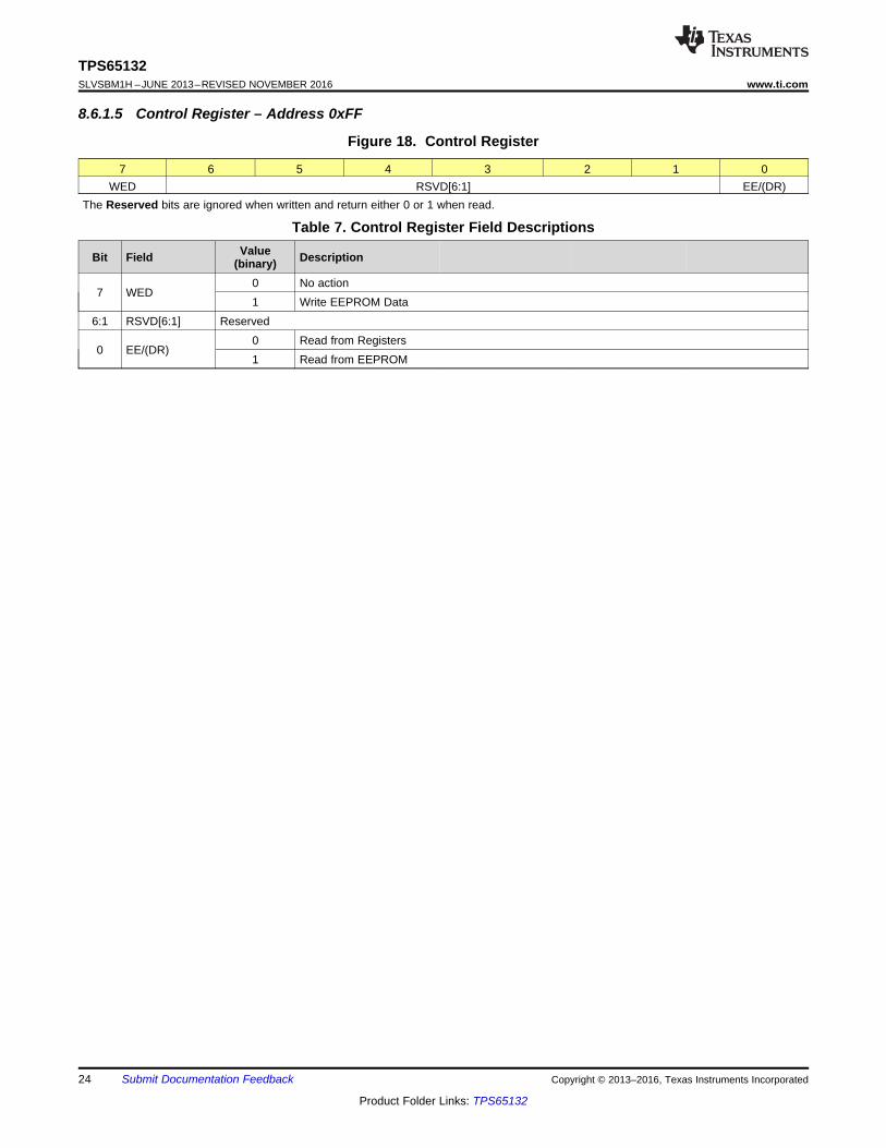
8.6.1.5 Control Register – Address 0xFF
Figure 18. Control Register
7 6 5 4 3 2 1 0WED RSVD[6:1] EE/(DR)
The Reserved bits are ignored when written and return either 0 or 1 when read.
Table 7. Control Register Field Descriptions
Bit Field Value(binary) Description
7 WED0 No action1 Write EEPROM Data
6:1 RSVD[6:1] Reserved
0 EE/(DR)0 Read from Registers1 Read from EEPROM
25
TPS65132www.ti.com SLVSBM1H –JUNE 2013–REVISED NOVEMBER 2016
Product Folder Links: TPS65132
Submit Documentation FeedbackCopyright © 2013–2016, Texas Instruments Incorporated
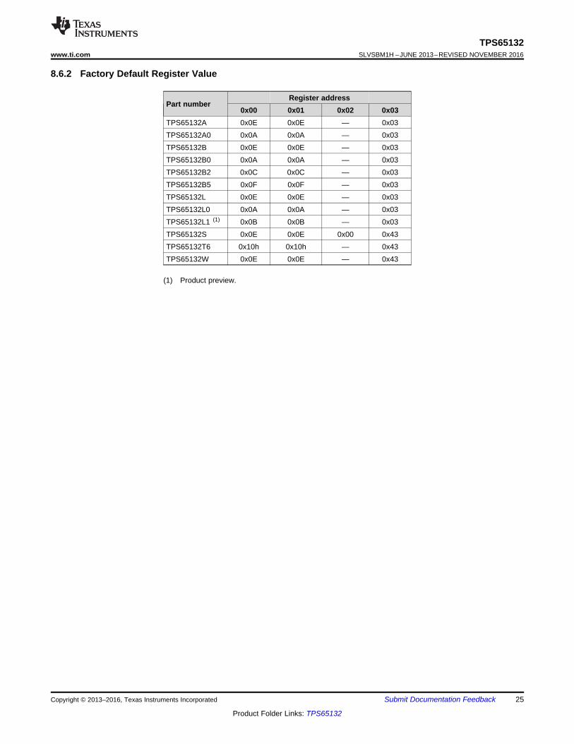
8.6.2 Factory Default Register Value
(1) Product preview.
Part numberRegister address
0x00 0x01 0x02 0x03TPS65132A 0x0E 0x0E — 0x03TPS65132A0 0x0A 0x0A — 0x03TPS65132B 0x0E 0x0E — 0x03TPS65132B0 0x0A 0x0A — 0x03TPS65132B2 0x0C 0x0C — 0x03TPS65132B5 0x0F 0x0F — 0x03TPS65132L 0x0E 0x0E — 0x03TPS65132L0 0x0A 0x0A — 0x03TPS65132L1 (1) 0x0B 0x0B — 0x03TPS65132S 0x0E 0x0E 0x00 0x43TPS65132T6 0x10h 0x10h — 0x43TPS65132W 0x0E 0x0E — 0x43
C1
C3
C2
C4
C5
4.7 µF
L
4.7 µH
ENP
ENN
OUTP
REG
SW
PGND
VIN
VPOS
VNEG
2.5V to 5.5 V
SCL
SDA
5.4 V/40 mA
OUTN
CFLY1
CFLY2
–5.4 V/40 mA
AGND
4.7 µF
4.7 µF
4.7 µF
2.2 µF
VIN
26
TPS65132SLVSBM1H –JUNE 2013–REVISED NOVEMBER 2016 www.ti.com
Product Folder Links: TPS65132
Submit Documentation Feedback Copyright © 2013–2016, Texas Instruments Incorporated
9 Application and Implementation
NOTEInformation in the following applications sections is not part of the TI componentspecification, and TI does not warrant its accuracy or completeness. TI’s customers areresponsible for determining suitability of components for their purposes. Customers shouldvalidate and test their design implementation to confirm system functionality.
9.1 Application InformationThe TPS65132xx devices, primarily intended to supplying TFT LCD displays, can be used for any applicationthat requires positive and negative supplies, ranging from ±4 V to ±6 V and current up to 80 mA (150 mA for theTPS65132Sx version). Both output voltages can be set independently and their sequencing is also independent.The following section presents the different operating modes that the device can support as well as the differentfeatures that the user can select.
9.2 Typical Applications
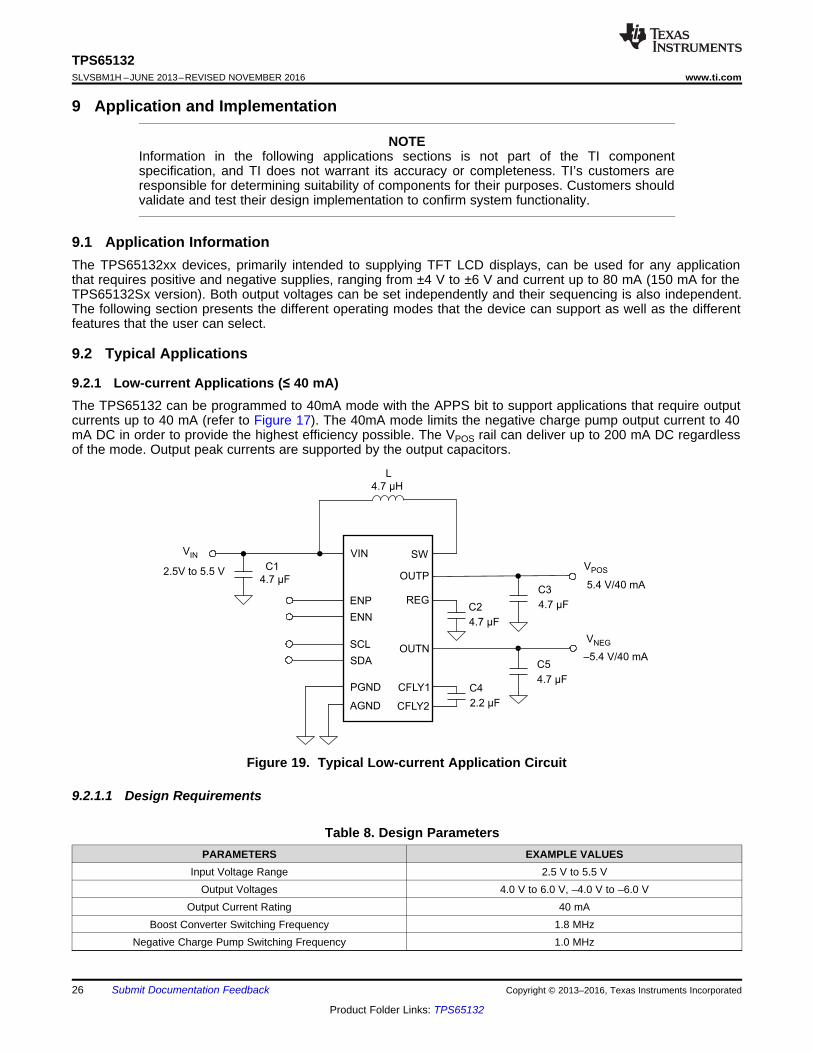
9.2.1 Low-current Applications (≤ 40 mA)The TPS65132 can be programmed to 40mA mode with the APPS bit to support applications that require outputcurrents up to 40 mA (refer to Figure 17). The 40mA mode limits the negative charge pump output current to 40mA DC in order to provide the highest efficiency possible. The VPOS rail can deliver up to 200 mA DC regardlessof the mode. Output peak currents are supported by the output capacitors.
Figure 19. Typical Low-current Application Circuit
9.2.1.1 Design Requirements
Table 8. Design ParametersPARAMETERS EXAMPLE VALUES
Input Voltage Range 2.5 V to 5.5 VOutput Voltages 4.0 V to 6.0 V, –4.0 V to –6.0 V
Output Current Rating 40 mABoost Converter Switching Frequency 1.8 MHz
Negative Charge Pump Switching Frequency 1.0 MHz
1
OUT LSWPEAK
I II = +
D 2
D
-
( )12
LOUT_max LIM_min
II = I D
Dæ ö+ ´ -ç ÷
è ø
f
´
´
IN_minL
SW
V DΔI =
L
´
-IN_min
S
V ηD = 1
VVREG
27
TPS65132www.ti.com SLVSBM1H –JUNE 2013–REVISED NOVEMBER 2016
Product Folder Links: TPS65132
Submit Documentation FeedbackCopyright © 2013–2016, Texas Instruments Incorporated
9.2.1.2 Detailed Design Procedure
9.2.1.2.1 Sequencing
Each output rail (VPOS and VNEG) is enabled and disabled using an external enable signal. If not explicitlyspecified, the enable signal in the rest of the document refers to ENN or ENP: ENP for the positive rail VPOS andENN for the negative rail VNEG. Figure 33 to Figure 36 show the typical sequencing waveforms.
NOTEIn the case where VIN falls below the UVLO threshold while one of the enable signals isstill high, all converters will be shut down instantaneously and both VPOS and VNEG outputrails will be actively discharged to GND.
9.2.1.2.2 Boost Converter Design Procedure
The first step in the design procedure is to verify whether the maximum possible output current of the boostconverter supports the specific application requirements. A simple approach is to estimate the converterefficiency, by taking the efficiency number from the provided efficiency curves at the application's maximum loador to use a worst case assumption for the expected efficiency, e.g., 85%.
1. Duty Cycle:
2. Inductor ripple current:
3. Maximum output current:
4. Peak switch current of the application:
η = Estimated boost converter efficiency (use the number from the efficiency plots or 85% as an estimation)ƒSW = Boost converter switching frequency (1.8 MHz)L = Selected inductor value for the boost converter (see the Inductor Selection section)ISWPEAK = Boost converter switch current at the desired output current (must be < [ ILIM_min + ΔIL])ΔIL = Inductor peak-to-peak ripple currentVREG = max (VPOS, |VNEG|) + 200 mV (in 40mA mode — + 300 mV in 80mA mode — + 500 mV withTPS65132Sx with SYNC = HIGH)IOUT = IOUT_VPOS + | IOUT_VNEG| (IOUT_max being the maximum current delivered on each rail)
The peak switch current is the current that the integrated switch and the inductor have to handle. The calculationmust be done for the minimum input voltage where the peak switch current is highest.
9.2.1.2.2.1 Inductor Selection (Boost Converter)
Saturation current: the inductor must handle the maximum peak current (IL_SAT > ISWPEAK, or IL_SAT > [ ILIM_min +ΔIL] as conservative approach)
DC Resistance: the lower the DCR, the lower the losses
Inductor value: in order to keep the ratio IOUT/ΔIL low enough for proper sensing operation purpose, it isrecommended to use a 4.7 µH inductor for 40mA mode (a 2.2 µH might however be used, but the efficiencymight be lower than with 4.7 µH at light loads depending on the inductor characteristics).
28
TPS65132SLVSBM1H –JUNE 2013–REVISED NOVEMBER 2016 www.ti.com
Product Folder Links: TPS65132
Submit Documentation Feedback Copyright © 2013–2016, Texas Instruments Incorporated
(1) See Third-Party Products Disclaimer
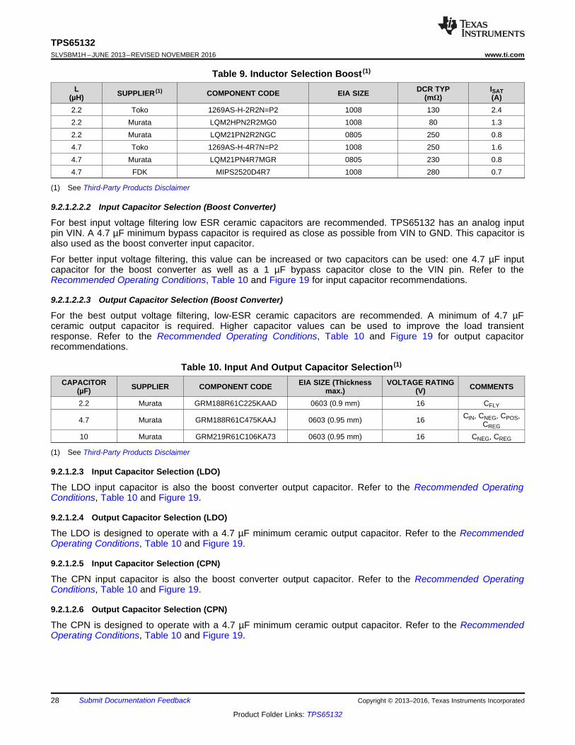
Table 9. Inductor Selection Boost (1)
L(µH) SUPPLIER (1) COMPONENT CODE EIA SIZE DCR TYP
(mΩ)ISAT(A)
2.2 Toko 1269AS-H-2R2N=P2 1008 130 2.42.2 Murata LQM2HPN2R2MG0 1008 80 1.32.2 Murata LQM21PN2R2NGC 0805 250 0.84.7 Toko 1269AS-H-4R7N=P2 1008 250 1.64.7 Murata LQM21PN4R7MGR 0805 230 0.84.7 FDK MIPS2520D4R7 1008 280 0.7
(1) See Third-Party Products Disclaimer
9.2.1.2.2.2 Input Capacitor Selection (Boost Converter)
For best input voltage filtering low ESR ceramic capacitors are recommended. TPS65132 has an analog inputpin VIN. A 4.7 µF minimum bypass capacitor is required as close as possible from VIN to GND. This capacitor isalso used as the boost converter input capacitor.
For better input voltage filtering, this value can be increased or two capacitors can be used: one 4.7 µF inputcapacitor for the boost converter as well as a 1 µF bypass capacitor close to the VIN pin. Refer to theRecommended Operating Conditions, Table 10 and Figure 19 for input capacitor recommendations.
9.2.1.2.2.3 Output Capacitor Selection (Boost Converter)
For the best output voltage filtering, low-ESR ceramic capacitors are recommended. A minimum of 4.7 µFceramic output capacitor is required. Higher capacitor values can be used to improve the load transientresponse. Refer to the Recommended Operating Conditions, Table 10 and Figure 19 for output capacitorrecommendations.
Table 10. Input And Output Capacitor Selection (1)
CAPACITOR(µF) SUPPLIER COMPONENT CODE EIA SIZE (Thickness
max.)VOLTAGE RATING
(V) COMMENTS
2.2 Murata GRM188R61C225KAAD 0603 (0.9 mm) 16 CFLY
4.7 Murata GRM188R61C475KAAJ 0603 (0.95 mm) 16 CIN, CNEG, CPOS,CREG
10 Murata GRM219R61C106KA73 0603 (0.95 mm) 16 CNEG, CREG
9.2.1.2.3 Input Capacitor Selection (LDO)
The LDO input capacitor is also the boost converter output capacitor. Refer to the Recommended OperatingConditions, Table 10 and Figure 19.
9.2.1.2.4 Output Capacitor Selection (LDO)
The LDO is designed to operate with a 4.7 µF minimum ceramic output capacitor. Refer to the RecommendedOperating Conditions, Table 10 and Figure 19.
9.2.1.2.5 Input Capacitor Selection (CPN)
The CPN input capacitor is also the boost converter output capacitor. Refer to the Recommended OperatingConditions, Table 10 and Figure 19.
9.2.1.2.6 Output Capacitor Selection (CPN)
The CPN is designed to operate with a 4.7 µF minimum ceramic output capacitor. Refer to the RecommendedOperating Conditions, Table 10 and Figure 19.
29
TPS65132www.ti.com SLVSBM1H –JUNE 2013–REVISED NOVEMBER 2016
Product Folder Links: TPS65132
Submit Documentation FeedbackCopyright © 2013–2016, Texas Instruments Incorporated
(1) See Third-Party Products Disclaimer
9.2.1.2.7 Flying Capacitor Selection (CPN)
The CPN needs an external flying capacitor. The minimum value is 2.2 µF. Special care must be taken whilechoosing the flying capacitor as it will directly impact the output voltage accuracy and load regulationperformance. Therefore, a minimum capacitance of 1 µF must be achieved by the capacitor at a DC bias voltageof │VNEG│ + 300 mV. For proper operation, the flying capacitor value must be lower than the output capacitor ofthe boost converter on REG pin.
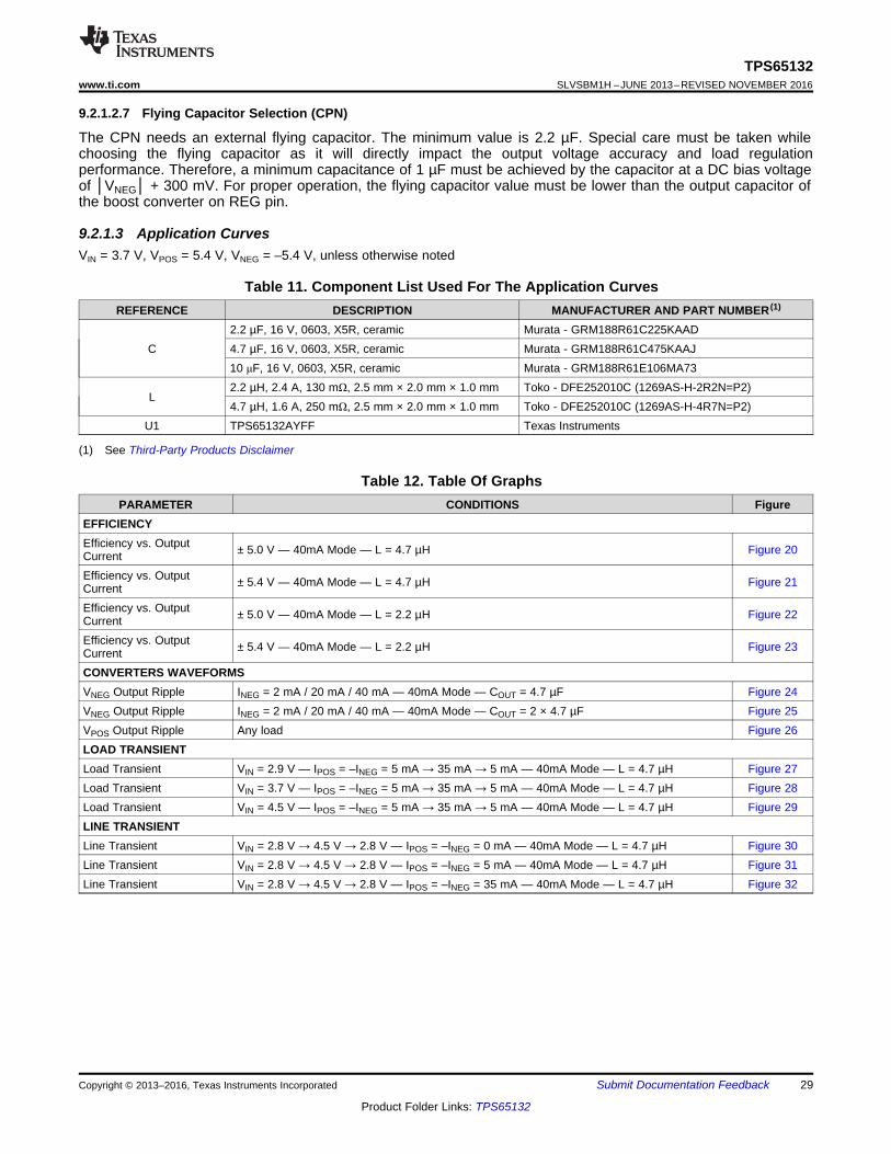
9.2.1.3 Application CurvesVIN = 3.7 V, VPOS = 5.4 V, VNEG = –5.4 V, unless otherwise noted
Table 11. Component List Used For The Application CurvesREFERENCE DESCRIPTION MANUFACTURER AND PART NUMBER (1)
C2.2 µF, 16 V, 0603, X5R, ceramic Murata - GRM188R61C225KAAD4.7 µF, 16 V, 0603, X5R, ceramic Murata - GRM188R61C475KAAJ10 μF, 16 V, 0603, X5R, ceramic Murata - GRM188R61E106MA73
L2.2 µH, 2.4 A, 130 mΩ, 2.5 mm × 2.0 mm × 1.0 mm Toko - DFE252010C (1269AS-H-2R2N=P2)4.7 µH, 1.6 A, 250 mΩ, 2.5 mm × 2.0 mm × 1.0 mm Toko - DFE252010C (1269AS-H-4R7N=P2)
U1 TPS65132AYFF Texas Instruments
Table 12. Table Of GraphsPARAMETER CONDITIONS Figure
EFFICIENCYEfficiency vs. OutputCurrent ± 5.0 V — 40mA Mode — L = 4.7 µH Figure 20
Efficiency vs. OutputCurrent ± 5.4 V — 40mA Mode — L = 4.7 µH Figure 21
Efficiency vs. OutputCurrent ± 5.0 V — 40mA Mode — L = 2.2 µH Figure 22
Efficiency vs. OutputCurrent ± 5.4 V — 40mA Mode — L = 2.2 µH Figure 23
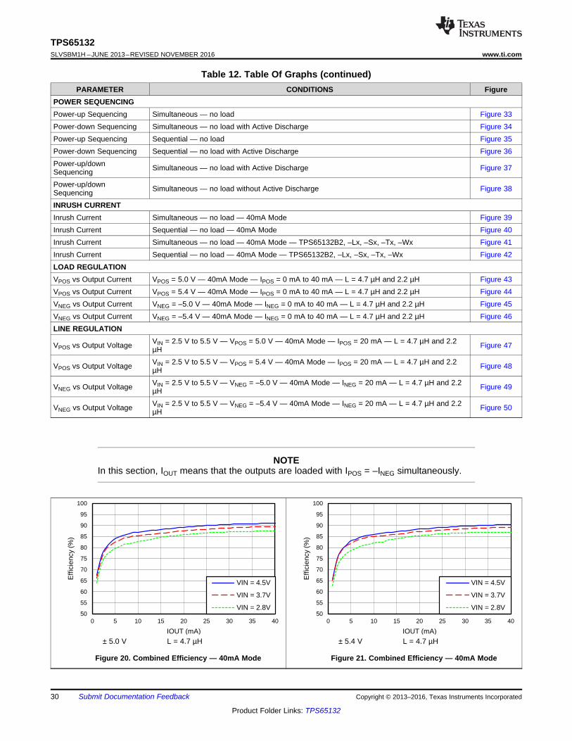
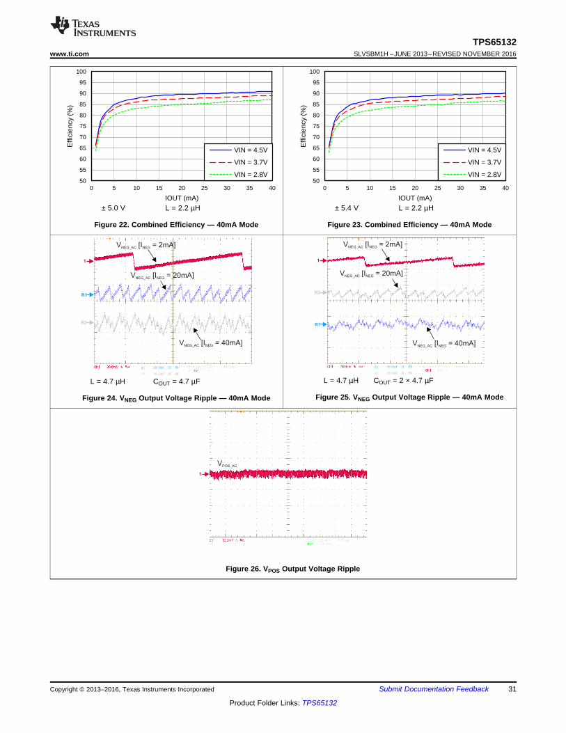
CONVERTERS WAVEFORMSVNEG Output Ripple INEG = 2 mA / 20 mA / 40 mA — 40mA Mode — COUT = 4.7 µF Figure 24VNEG Output Ripple INEG = 2 mA / 20 mA / 40 mA — 40mA Mode — COUT = 2 × 4.7 µF Figure 25VPOS Output Ripple Any load Figure 26LOAD TRANSIENTLoad Transient VIN = 2.9 V — IPOS = –INEG = 5 mA → 35 mA → 5 mA — 40mA Mode — L = 4.7 µH Figure 27Load Transient VIN = 3.7 V — IPOS = –INEG = 5 mA → 35 mA → 5 mA — 40mA Mode — L = 4.7 µH Figure 28Load Transient VIN = 4.5 V — IPOS = –INEG = 5 mA → 35 mA → 5 mA — 40mA Mode — L = 4.7 µH Figure 29LINE TRANSIENTLine Transient VIN = 2.8 V → 4.5 V → 2.8 V — IPOS = –INEG = 0 mA — 40mA Mode — L = 4.7 µH Figure 30Line Transient VIN = 2.8 V → 4.5 V → 2.8 V — IPOS = –INEG = 5 mA — 40mA Mode — L = 4.7 µH Figure 31Line Transient VIN = 2.8 V → 4.5 V → 2.8 V — IPOS = –INEG = 35 mA — 40mA Mode — L = 4.7 µH Figure 32
50
55
60
65
70
75
80
85
90
95
100
0 5 10 15 20 25 30 35 40
Effi
cien
cy (%
)
IOUT (mA)
VIN = 4.5V
VIN = 3.7V
VIN = 2.8V
C005
50
55
60
65
70
75
80
85
90
95
100
0 5 10 15 20 25 30 35 40
Effi
cien
cy (%
)
IOUT (mA)
VIN = 4.5V
VIN = 3.7V
VIN = 2.8V
C006
30
TPS65132SLVSBM1H –JUNE 2013–REVISED NOVEMBER 2016 www.ti.com
Product Folder Links: TPS65132
Submit Documentation Feedback Copyright © 2013–2016, Texas Instruments Incorporated
Table 12. Table Of Graphs (continued)PARAMETER CONDITIONS Figure
POWER SEQUENCINGPower-up Sequencing Simultaneous — no load Figure 33Power-down Sequencing Simultaneous — no load with Active Discharge Figure 34Power-up Sequencing Sequential — no load Figure 35Power-down Sequencing Sequential — no load with Active Discharge Figure 36Power-up/downSequencing Simultaneous — no load with Active Discharge Figure 37
Power-up/downSequencing Simultaneous — no load without Active Discharge Figure 38
INRUSH CURRENTInrush Current Simultaneous — no load — 40mA Mode Figure 39Inrush Current Sequential — no load — 40mA Mode Figure 40Inrush Current Simultaneous — no load — 40mA Mode — TPS65132B2, –Lx, –Sx, –Tx, –Wx Figure 41Inrush Current Sequential — no load — 40mA Mode — TPS65132B2, –Lx, –Sx, –Tx, –Wx Figure 42LOAD REGULATIONVPOS vs Output Current VPOS = 5.0 V — 40mA Mode — IPOS = 0 mA to 40 mA — L = 4.7 µH and 2.2 µH Figure 43VPOS vs Output Current VPOS = 5.4 V — 40mA Mode — IPOS = 0 mA to 40 mA — L = 4.7 µH and 2.2 µH Figure 44VNEG vs Output Current VNEG = –5.0 V — 40mA Mode — INEG = 0 mA to 40 mA — L = 4.7 µH and 2.2 µH Figure 45VNEG vs Output Current VNEG = –5.4 V — 40mA Mode — INEG = 0 mA to 40 mA — L = 4.7 µH and 2.2 µH Figure 46LINE REGULATION
VPOS vs Output Voltage VIN = 2.5 V to 5.5 V — VPOS = 5.0 V — 40mA Mode — IPOS = 20 mA — L = 4.7 µH and 2.2µH Figure 47
VPOS vs Output Voltage VIN = 2.5 V to 5.5 V — VPOS = 5.4 V — 40mA Mode — IPOS = 20 mA — L = 4.7 µH and 2.2µH Figure 48
VNEG vs Output Voltage VIN = 2.5 V to 5.5 V — VNEG = –5.0 V — 40mA Mode — INEG = 20 mA — L = 4.7 µH and 2.2µH Figure 49
VNEG vs Output Voltage VIN = 2.5 V to 5.5 V — VNEG = –5.4 V — 40mA Mode — INEG = 20 mA — L = 4.7 µH and 2.2µH Figure 50
spacer
NOTEIn this section, IOUT means that the outputs are loaded with IPOS = –INEG simultaneously.
± 5.0 V L = 4.7 µH
Figure 20. Combined Efficiency — 40mA Mode
± 5.4 V L = 4.7 µH
Figure 21. Combined Efficiency — 40mA Mode
1
VPOS_AC
1
R1
R1
R2
R2
20.0mV AC BW
20.0mV AC BW
V [I = 2mA]NEG_AC NEG
V [ = 20mA]NEG_AC INEG
V [ = 40mA]NEG_AC INEG
1
R1
R1
R2
R2
20.0mV AC BW
20.0mV AC BW
V [I = 2mA]NEG_AC NEG
V [ = 20mA]NEG_AC INEG
V [ = 40mA]NEG_AC INEG
50
55
60
65
70
75
80
85
90
95
100
0 5 10 15 20 25 30 35 40
Effi
cien
cy (%
)
IOUT (mA)
VIN = 4.5V
VIN = 3.7V
VIN = 2.8V
C003
50
55
60
65
70
75
80
85
90
95
100
0 5 10 15 20 25 30 35 40
Effi
cien
cy (%
)
IOUT (mA)
VIN = 4.5V
VIN = 3.7V
VIN = 2.8V
C004
31
TPS65132www.ti.com SLVSBM1H –JUNE 2013–REVISED NOVEMBER 2016
Product Folder Links: TPS65132
Submit Documentation FeedbackCopyright © 2013–2016, Texas Instruments Incorporated
± 5.0 V L = 2.2 µH
Figure 22. Combined Efficiency — 40mA Mode
± 5.4 V L = 2.2 µH
Figure 23. Combined Efficiency — 40mA Mode
L = 4.7 µH COUT = 4.7 µF
Figure 24. VNEG Output Voltage Ripple — 40mA Mode
L = 4.7 µH COUT = 2 × 4.7 µF
Figure 25. VNEG Output Voltage Ripple — 40mA Mode
Figure 26. VPOS Output Voltage Ripple
1
2
3
VNEG_AC
VPOS_AC
VIN
VNEG_AC
VPOS_AC
VIN
1
2
3
1
2
4
VNEG_AC
VPOS_AC
IPOS = - NEGI
1
2
3
VNEG_AC
VPOS_AC
VIN
1
2
4
VNEG_AC
VPOS_AC
IPOS = - NEGI
1
2
4
VNEG_AC
VPOS_AC
IPOS = - NEGI
32
TPS65132SLVSBM1H –JUNE 2013–REVISED NOVEMBER 2016 www.ti.com
Product Folder Links: TPS65132
Submit Documentation Feedback Copyright © 2013–2016, Texas Instruments Incorporated
VIN = 2.9 V ΔIOUT = 30 mA
Figure 27. Load Transient — 40mA Mode
VIN = 3.7 V ΔIOUT = 30 mA
Figure 28. Load Transient — 40mA Mode
VIN = 4.5 V ΔIOUT = 30 mA
Figure 29. Load Transient — 40mA Mode
IOUT = 0 mA ΔVIN = 1.7 V
Figure 30. Line Transient — 40mA Mode
IOUT = 5 mA ΔVIN = 1.7 V
Figure 31. Line Transient — 40mA Mode
IOUT = 35 mA ΔVIN = 1.7 V
Figure 32. Line Transient — 40mA Mode

1
2
43
R2
R2 5.0V
ENP
ENN
VSW
VPOS
VNEG
1
2
43
R2
R2 5.0V
ENP
ENN
VSW
VPOS
VNEG
1
2
43
R2
R2 5.0V
ENP
ENN
VREG
VPOS
VNEG
1
2
43
R2
R2 5.0V
ENP
ENN
VSW
VPOS
VNEG
1
2
43
R2
R2 5.0V
ENP
ENN
VREG
VPOS
VNEG
1
2
43
R2
R2 5.0V
ENP
ENN
VSW
VPOS
VNEG
33
TPS65132www.ti.com SLVSBM1H –JUNE 2013–REVISED NOVEMBER 2016
Product Folder Links: TPS65132
Submit Documentation FeedbackCopyright © 2013–2016, Texas Instruments Incorporated
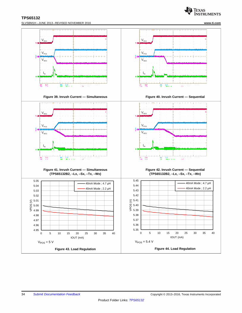
Figure 33. Power-Up Sequencing — Simultaneous Figure 34. Power-Down Sequencing — Simultaneous(with Active Discharge)
Figure 35. Power-Up Sequencing — Sequential Figure 36. Power-Down Sequencing — Sequential(with Active Discharge)
Figure 37. Power-Up/Down With Active Discharge Figure 38. Power-Up/Down Without Active Discharge(TPS65132Ax only)
4.95
4.96
4.97
4.98
4.99
5.00
5.01
5.02
5.03
5.04
5.05
0 5 10 15 20 25 30 35 40
VP
OS
(V
)
IOUT (mA)
40mA Mode ; 4.7 µH
40mA Mode ; 2.2 µH
C008
5.35
5.36
5.37
5.38
5.39
5.40
5.41
5.42
5.43
5.44
5.45
0 5 10 15 20 25 30 35 40
VP
OS
(V
)
IOUT (mA)
40mA Mode ; 4.7 µH
40mA Mode ; 2.2 µH
C009
1
2
4
3
VREG
VPOS
VNEG
IIN
1
2
4
3
VREG
VPOS
VNEG
IIN
1
2
4
3
VREG
VPOS
VNEG
IIN
1
2
4
3
VREG
VPOS
VNEG
IIN
34
TPS65132SLVSBM1H –JUNE 2013–REVISED NOVEMBER 2016 www.ti.com
Product Folder Links: TPS65132
Submit Documentation Feedback Copyright © 2013–2016, Texas Instruments Incorporated
Figure 39. Inrush Current — Simultaneous Figure 40. Inrush Current — Sequential
Figure 41. Inrush Current — Simultaneous(TPS65132B2, –Lx, –Sx, –Tx, –Wx)
Figure 42. Inrush Current — Sequential(TPS65132B2, –Lx, –Sx, –Tx, –Wx)
VPOS = 5 V
Figure 43. Load Regulation
VPOS = 5.4 V
Figure 44. Load Regulation
-5.01
-5.00
-4.99
-4.98
-4.97
-4.96
2.5 2.7 2.9 3.1 3.3 3.5 3.7 3.9 4.1 4.3 4.5 4.7 4.9 5.1 5.3 5.5
VN
EG
(V
)
VIN (V)
40mA Mode ; 4.7 µH
40mA Mode ; 2.2 µH
C01
-5.41
-5.40
-5.39
-5.38
-5.37
-5.36
2.5 2.7 2.9 3.1 3.3 3.5 3.7 3.9 4.1 4.3 4.5 4.7 4.9 5.1 5.3 5.5
VN
EG
(V
)
VIN (V)
40mA Mode ; 4.7 µH
40mA Mode ; 2.2 µH
C01
4.97
4.98
4.99
5.00
5.01
5.02
2.5 2.7 2.9 3.1 3.3 3.5 3.7 3.9 4.1 4.3 4.5 4.7 4.9 5.1 5.3 5.5
VP
OS
(V
)
VIN (V)
40mA Mode ; 4.7 µH
40mA Mode ; 2.2 µH
C01
5.37
5.38
5.39
5.40
5.41
5.42
2.5 2.7 2.9 3.1 3.3 3.5 3.7 3.9 4.1 4.3 4.5 4.7 4.9 5.1 5.3 5.5
VP
OS
(V
)
VIN (V)
40mA Mode ; 4.7 µH
40mA Mode ; 2.2 µH
C01
-5.05
-5.04
-5.03
-5.02
-5.01
-5.00
-4.99
-4.98
-4.97
-4.96
-4.95
0 5 10 15 20 25 30 35 40
VN
EG
(V
)
IOUT (mA)
40mA Mode ; 4.7 µH
40mA Mode ; 2.2 µH
C01
-5.45
-5.44
-5.43
-5.42
-5.41
-5.40
-5.39
-5.38
-5.37
-5.36
-5.35
0 5 10 15 20 25 30 35 40
VN
EG
(V
)
IOUT (mA)
40mA Mode ; 4.7 µH
40mA Mode ; 2.2 µH
C01
35
TPS65132www.ti.com SLVSBM1H –JUNE 2013–REVISED NOVEMBER 2016
Product Folder Links: TPS65132
Submit Documentation FeedbackCopyright © 2013–2016, Texas Instruments Incorporated
VNEG = –5 V
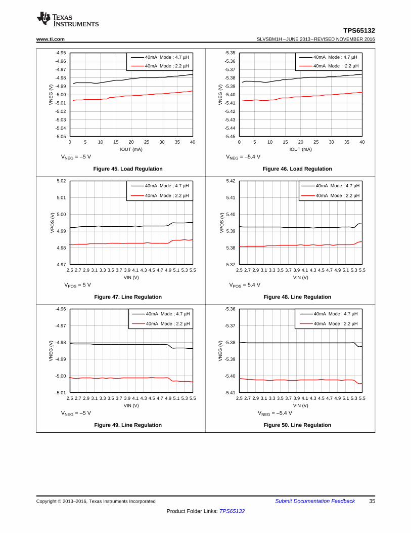
Figure 45. Load Regulation
VNEG = –5.4 V
Figure 46. Load Regulation
VPOS = 5 V
Figure 47. Line Regulation
VPOS = 5.4 V
Figure 48. Line Regulation
VNEG = –5 V
Figure 49. Line Regulation
VNEG = –5.4 V
Figure 50. Line Regulation
C1
C3
C2
C4
C5
4.7 µF
L
2.2 µH
ENP
ENN
OUTP
REG
SW
PGND
VIN
VPOS
VNEG
2.5V to 5.5 V
SCL
SDA
5.4 V/80 mA
OUTN
CFLY1
CFLY2
–5.4 V/80 mA
AGND
10 µF
10 µF
10 µF
4.7 µF
VIN
36
TPS65132SLVSBM1H –JUNE 2013–REVISED NOVEMBER 2016 www.ti.com
Product Folder Links: TPS65132
Submit Documentation Feedback Copyright © 2013–2016, Texas Instruments Incorporated
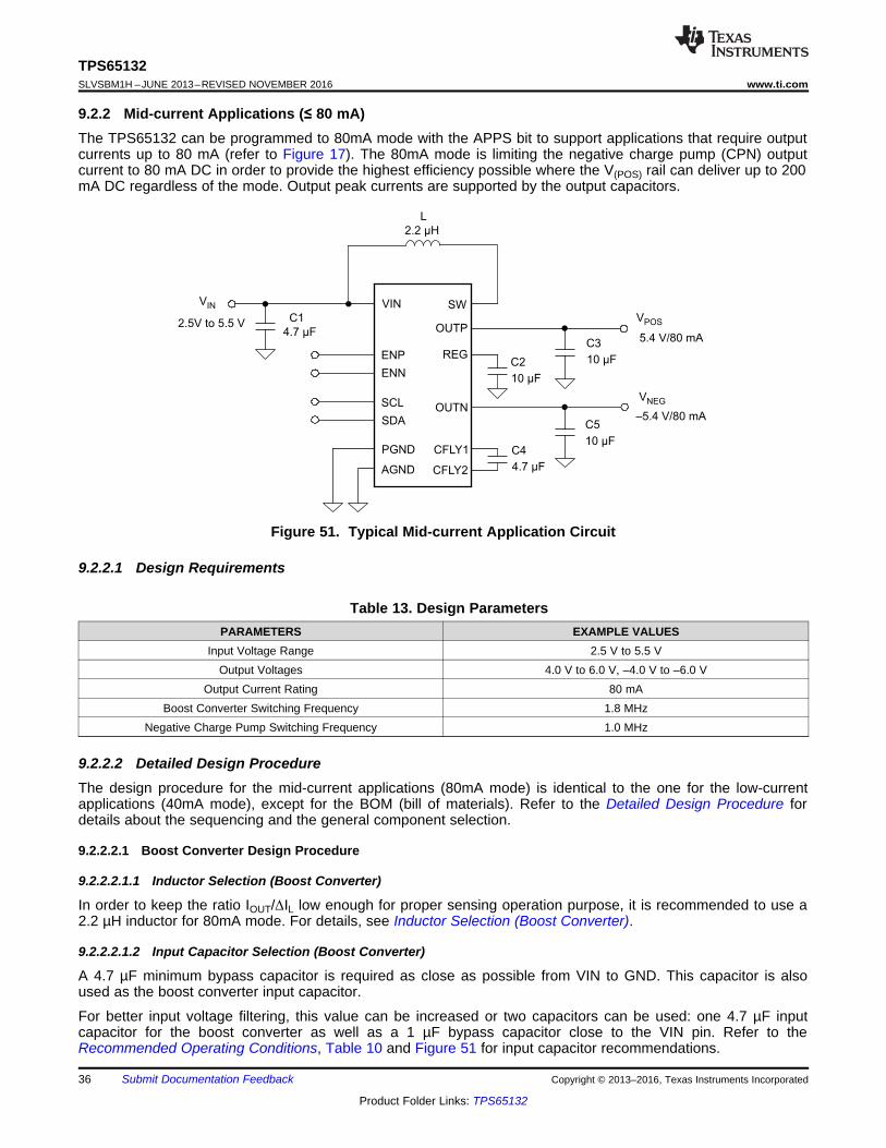
9.2.2 Mid-current Applications (≤ 80 mA)The TPS65132 can be programmed to 80mA mode with the APPS bit to support applications that require outputcurrents up to 80 mA (refer to Figure 17). The 80mA mode is limiting the negative charge pump (CPN) outputcurrent to 80 mA DC in order to provide the highest efficiency possible where the V(POS) rail can deliver up to 200mA DC regardless of the mode. Output peak currents are supported by the output capacitors.
Figure 51. Typical Mid-current Application Circuit
9.2.2.1 Design Requirements
Table 13. Design ParametersPARAMETERS EXAMPLE VALUES
Input Voltage Range 2.5 V to 5.5 VOutput Voltages 4.0 V to 6.0 V, –4.0 V to –6.0 V
Output Current Rating 80 mABoost Converter Switching Frequency 1.8 MHz
Negative Charge Pump Switching Frequency 1.0 MHz
9.2.2.2 Detailed Design ProcedureThe design procedure for the mid-current applications (80mA mode) is identical to the one for the low-currentapplications (40mA mode), except for the BOM (bill of materials). Refer to the Detailed Design Procedure fordetails about the sequencing and the general component selection.
9.2.2.2.1 Boost Converter Design Procedure
9.2.2.2.1.1 Inductor Selection (Boost Converter)
In order to keep the ratio IOUT/ΔIL low enough for proper sensing operation purpose, it is recommended to use a2.2 µH inductor for 80mA mode. For details, see Inductor Selection (Boost Converter).
9.2.2.2.1.2 Input Capacitor Selection (Boost Converter)
A 4.7 µF minimum bypass capacitor is required as close as possible from VIN to GND. This capacitor is alsoused as the boost converter input capacitor.
For better input voltage filtering, this value can be increased or two capacitors can be used: one 4.7 µF inputcapacitor for the boost converter as well as a 1 µF bypass capacitor close to the VIN pin. Refer to theRecommended Operating Conditions, Table 10 and Figure 51 for input capacitor recommendations.
37
TPS65132www.ti.com SLVSBM1H –JUNE 2013–REVISED NOVEMBER 2016
Product Folder Links: TPS65132
Submit Documentation FeedbackCopyright © 2013–2016, Texas Instruments Incorporated
(1) See Third-Party Products Disclaimer
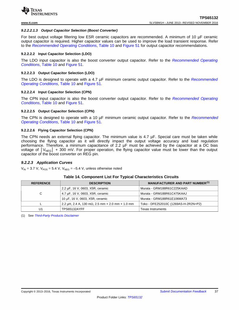
9.2.2.2.1.3 Output Capacitor Selection (Boost Converter)
For best output voltage filtering low ESR ceramic capacitors are recommended. A minimum of 10 µF ceramicoutput capacitor is required. Higher capacitor values can be used to improve the load transient response. Referto the Recommended Operating Conditions, Table 10 and Figure 51 for output capacitor recommendations.
9.2.2.2.2 Input Capacitor Selection (LDO)
The LDO input capacitor is also the boost converter output capacitor. Refer to the Recommended OperatingConditions, Table 10 and Figure 51.
9.2.2.2.3 Output Capacitor Selection (LDO)
The LDO is designed to operate with a 4.7 µF minimum ceramic output capacitor. Refer to the RecommendedOperating Conditions, Table 10 and Figure 51.
9.2.2.2.4 Input Capacitor Selection (CPN)
The CPN input capacitor is also the boost converter output capacitor. Refer to the Recommended OperatingConditions, Table 10 and Figure 51.
9.2.2.2.5 Output Capacitor Selection (CPN)
The CPN is designed to operate with a 10 µF minimum ceramic output capacitor. Refer to the RecommendedOperating Conditions, Table 10 and Figure 51.
9.2.2.2.6 Flying Capacitor Selection (CPN)
The CPN needs an external flying capacitor. The minimum value is 4.7 µF. Special care must be taken whilechoosing the flying capacitor as it will directly impact the output voltage accuracy and load regulationperformance. Therefore, a minimum capacitance of 2.2 µF must be achieved by the capacitor at a DC biasvoltage of │VNEG│ + 300 mV. For proper operation, the flying capacitor value must be lower than the outputcapacitor of the boost converter on REG pin.
9.2.2.3 Application CurvesVIN = 3.7 V, VPOS = 5.4 V, VNEG = –5.4 V, unless otherwise noted
Table 14. Component List For Typical Characteristics CircuitsREFERENCE DESCRIPTION MANUFACTURER AND PART NUMBER (1)
C2.2 µF, 16 V, 0603, X5R, ceramic Murata - GRM188R61C225KAAD4.7 µF, 16 V, 0603, X5R, ceramic Murata - GRM188R61C475KAAJ10 μF, 16 V, 0603, X5R, ceramic Murata - GRM188R61E106MA73
L 2.2 µH, 2.4 A, 130 mΩ, 2.5 mm × 2.0 mm × 1.0 mm Toko - DFE252010C (1269AS-H-2R2N=P2)U1 TPS65132AYFF Texas Instruments
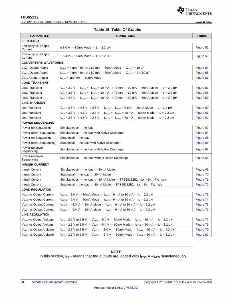
38
TPS65132SLVSBM1H –JUNE 2013–REVISED NOVEMBER 2016 www.ti.com
Product Folder Links: TPS65132
Submit Documentation Feedback Copyright © 2013–2016, Texas Instruments Incorporated
Table 15. Table Of GraphsPARAMETER CONDITIONS Figure
EFFICIENCYEfficiency vs. OutputCurrent ± 5.0 V — 80mA Mode — L = 2.2 µH Figure 52
Efficiency vs. OutputCurrent ± 5.4 V — 80mA Mode — L = 2.2 µH Figure 53
CONVERTERS WAVEFORMSVNEG Output Ripple INEG = 4 mA / 40 mA / 80 mA — 80mA Mode — COUT = 10 µF Figure 54VNEG Output Ripple INEG = 4 mA / 40 mA / 80 mA — 80mA Mode — COUT = 2 × 10 µF Figure 55VPOS Output Ripple IPOS = 150 mA — 80mA Mode Figure 56LOAD TRANSIENTLoad Transient VIN = 2.9 V — IPOS = –INEG = 10 mA → 70 mA → 10 mA — 80mA Mode — L = 2.2 µH Figure 57Load Transient VIN = 3.7 V — IPOS = –INEG = 10 mA → 70 mA → 10 mA — 80mA Mode — L = 2.2 µH Figure 58Load Transient VIN = 4.5 V — IPOS = –INEG = 10 mA → 70 mA → 10 mA — 80mA Mode — L = 2.2 µH Figure 59LINE TRANSIENTLine Transient VIN = 2.8 V → 4.5 V → 2.8 V — IPOS = –INEG = 0 mA — 80mA Mode — L = 2.2 µH Figure 60Line Transient VIN = 2.8 V → 4.5 V → 2.8 V — IPOS = –INEG = 40 mA — 80mA Mode — L = 2.2 µH Figure 61Line Transient VIN = 2.8 V → 4.5 V → 2.8 V — IPOS = –INEG = 70 mA — 80mA Mode — L = 2.2 µH Figure 62POWER SEQUENCINGPower-up Sequencing Simultaneous — no load Figure 63Power-down Sequencing Simultaneous — no load with Active Discharge Figure 64Power-up Sequencing Sequential — no load Figure 65Power-down Sequencing Sequential — no load with Active Discharge Figure 66Power-up/downSequencing Simultaneous — no load with Active Discharge Figure 67
Power-up/downSequencing Simultaneous — no load without Active Discharge Figure 68
INRUSH CURRENTInrush Current Simultaneous — no load — 80mA Mode Figure 69Inrush Current Sequential — no load — 80mA Mode Figure 70Inrush Current Simultaneous — no load — 80mA Mode — TPS65132B2, –Lx, –Sx, –Tx, –Wx Figure 71Inrush Current Sequential — no load — 80mA Mode — TPS65132B2, –Lx, –Sx, –Tx, –Wx Figure 72LOAD REGULATIONVPOS vs Output Current VPOS = 5.0 V — 80mA Mode — IPOS = 0 mA to 80 mA — L = 2.2 µH Figure 73VPOS vs Output Current VPOS = 5.4 V — 80mA Mode — IPOS = 0 mA to 80 mA — L = 2.2 µH Figure 74VNEG vs Output Current VNEG = –5.0 V — 80mA Mode — INEG = 0 mA to 80 mA — L = 2.2 µH Figure 75VNEG vs Output Current VNEG = –5.4 V — 80mA Mode — INEG = 0 mA to 80 mA — L = 2.2 µH Figure 76LINE REGULATIONVPOS vs Output Voltage VIN = 2.5 V to 5.5 V — VPOS = 5.0 V — 80mA Mode — IPOS = 60 mA — L = 2.2 µH Figure 77VPOS vs Output Voltage VIN = 2.5 V to 5.5 V — VPOS = 5.4 V — 80mA Mode — IPOS = 60 mA — L = 2.2 µH Figure 78VNEG vs Output Voltage VIN = 2.5 V to 5.5 V — VNEG = –5.0 V — 80mA Mode — INEG = 60 mA — L = 2.2 µH Figure 79VNEG vs Output Voltage VIN = 2.5 V to 5.5 V — VNEG = –5.4 V — 80mA Mode — INEG = 60 mA — L = 2.2 µH Figure 80
spacer
NOTEIn this section, IOUT means that the outputs are loaded with IPOS = –INEG simultaneously.
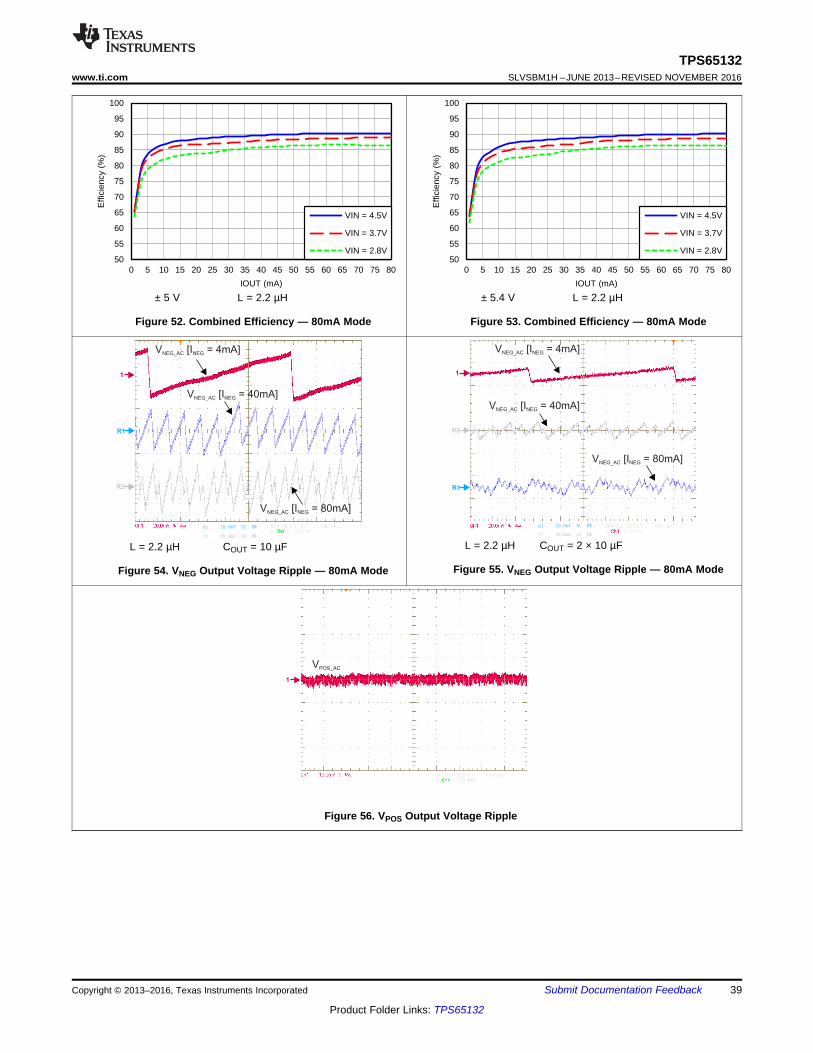
1
VPOS_AC
1
R1
R1
R2
R2
20.0mV AC BW
20.0mV AC BW
V [I = 4mA]NEG_AC NEG
V [ = 40mA]NEG_AC INEG
V [ = 80mA]NEG_AC INEG
1
R1
R2
V [I = 4mA]NEG_AC NEG
V [ = 40mA]NEG_AC INEG
V [ = 80mA]NEG_AC INEG
R1
R2
20.0mV AC BW
20.0mV AC BW
50
55
60
65
70
75
80
85
90
95
100
0 5 10 15 20 25 30 35 40 45 50 55 60 65 70 75 80
Effi
cien
cy (
%)
IOUT (mA)
VIN = 4.5V
VIN = 3.7V
VIN = 2.8V
C001
50
55
60
65
70
75
80
85
90
95
100
0 5 10 15 20 25 30 35 40 45 50 55 60 65 70 75 80
Effi
cien
cy (
%)
IOUT (mA)
VIN = 4.5V
VIN = 3.7V
VIN = 2.8V
C002
39
TPS65132www.ti.com SLVSBM1H –JUNE 2013–REVISED NOVEMBER 2016
Product Folder Links: TPS65132
Submit Documentation FeedbackCopyright © 2013–2016, Texas Instruments Incorporated
± 5 V L = 2.2 µH
Figure 52. Combined Efficiency — 80mA Mode
± 5.4 V L = 2.2 µH
Figure 53. Combined Efficiency — 80mA Mode
L = 2.2 µH COUT = 10 µF
Figure 54. VNEG Output Voltage Ripple — 80mA Mode
L = 2.2 µH COUT = 2 × 10 µF
Figure 55. VNEG Output Voltage Ripple — 80mA Mode
Figure 56. VPOS Output Voltage Ripple
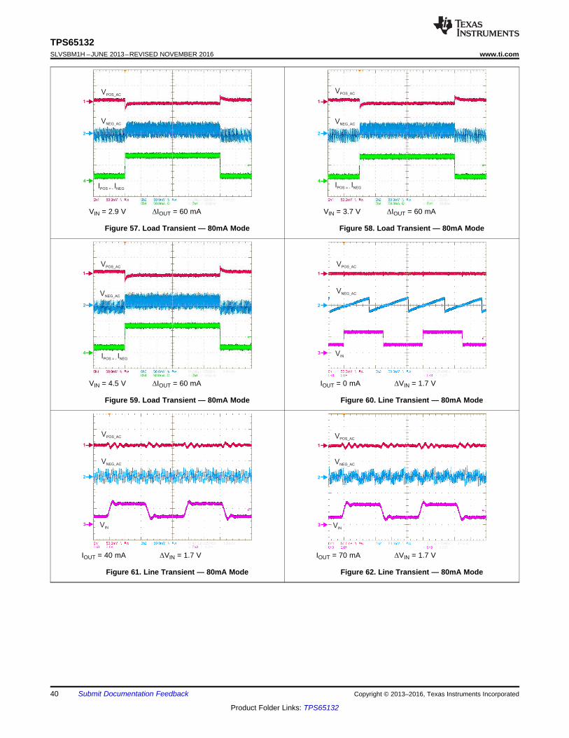
VNEG_AC
VPOS_AC
VIN
1
2
3
VNEG_AC
VPOS_AC
VIN
1
2
3
1
2
4
VNEG_AC
VPOS_AC
IPOS = - NEGI
VNEG_AC
VPOS_AC
VIN
1
2
3
1
2
4
VNEG_AC
VPOS_AC
IPOS = - NEGI
1
2
4
VNEG_AC
VPOS_AC
IPOS = - NEGI
40
TPS65132SLVSBM1H –JUNE 2013–REVISED NOVEMBER 2016 www.ti.com
Product Folder Links: TPS65132
Submit Documentation Feedback Copyright © 2013–2016, Texas Instruments Incorporated
VIN = 2.9 V ΔIOUT = 60 mA
Figure 57. Load Transient — 80mA Mode
VIN = 3.7 V ΔIOUT = 60 mA
Figure 58. Load Transient — 80mA Mode
VIN = 4.5 V ΔIOUT = 60 mA
Figure 59. Load Transient — 80mA Mode
IOUT = 0 mA ΔVIN = 1.7 V
Figure 60. Line Transient — 80mA Mode
IOUT = 40 mA ΔVIN = 1.7 V
Figure 61. Line Transient — 80mA Mode
IOUT = 70 mA ΔVIN = 1.7 V
Figure 62. Line Transient — 80mA Mode
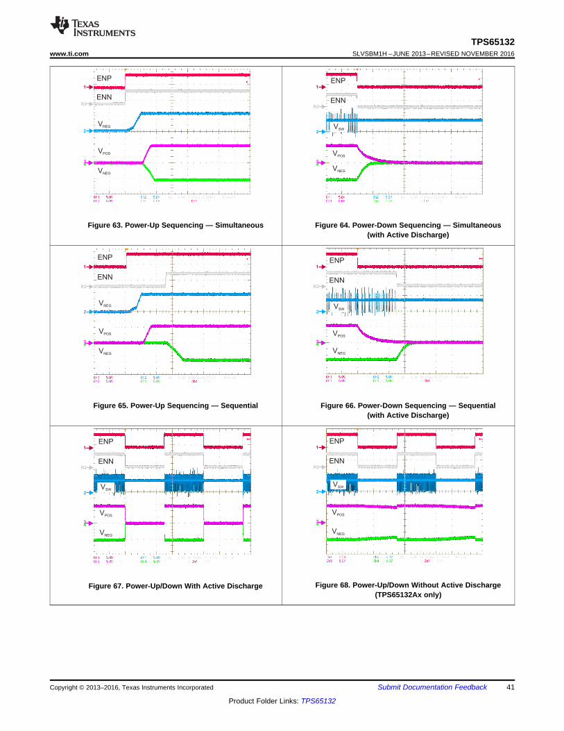
1
2
43
R2
R2 5.0V
ENP
ENN
VSW
VPOS
VNEG
1
2
43
R2
R2 5.0V
ENP
ENN
VSW
VPOS
VNEG
1
2
43
R2
R2 5.0V
ENP
ENN
VREG
VPOS
VNEG
1
2
43
R2
R2 5.0V
ENP
ENN
VSW
VPOS
VNEG
1
2
43
R2
R2 5.0V
ENP
ENN
VREG
VPOS
VNEG
1
2
43
R2
R2 5.0V
ENP
ENN
VSW
VPOS
VNEG
41
TPS65132www.ti.com SLVSBM1H –JUNE 2013–REVISED NOVEMBER 2016
Product Folder Links: TPS65132
Submit Documentation FeedbackCopyright © 2013–2016, Texas Instruments Incorporated
Figure 63. Power-Up Sequencing — Simultaneous Figure 64. Power-Down Sequencing — Simultaneous(with Active Discharge)
Figure 65. Power-Up Sequencing — Sequential Figure 66. Power-Down Sequencing — Sequential(with Active Discharge)
Figure 67. Power-Up/Down With Active Discharge Figure 68. Power-Up/Down Without Active Discharge(TPS65132Ax only)
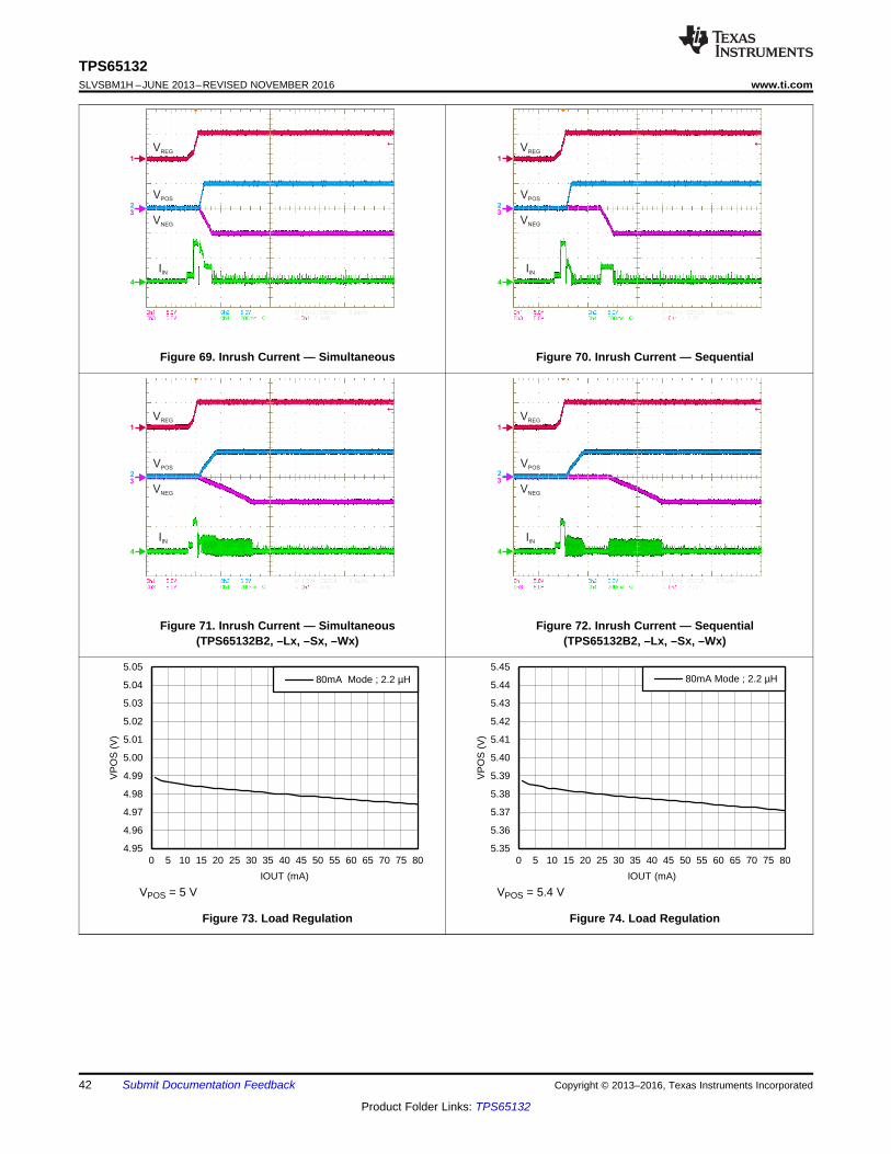
4.95
4.96
4.97
4.98
4.99
5.00
5.01
5.02
5.03
5.04
5.05
0 5 10 15 20 25 30 35 40 45 50 55 60 65 70 75 80
VP
OS
(V
)
IOUT (mA)
80mA Mode ; 2.2 µH
C016
5.35
5.36
5.37
5.38
5.39
5.40
5.41
5.42
5.43
5.44
5.45
0 5 10 15 20 25 30 35 40 45 50 55 60 65 70 75 80
VP
OS
(V
)
IOUT (mA)
80mA Mode ; 2.2 µH
C017
1
2
4
3
VREG
VPOS
VNEG
IIN
1
2
4
3
VREG
VPOS
VNEG
IIN
1
2
4
3
VREG
VPOS
VNEG
IIN
1
2
4
3
VREG
VPOS
VNEG
IIN
42
TPS65132SLVSBM1H –JUNE 2013–REVISED NOVEMBER 2016 www.ti.com
Product Folder Links: TPS65132
Submit Documentation Feedback Copyright © 2013–2016, Texas Instruments Incorporated
Figure 69. Inrush Current — Simultaneous Figure 70. Inrush Current — Sequential
Figure 71. Inrush Current — Simultaneous(TPS65132B2, –Lx, –Sx, –Wx)
Figure 72. Inrush Current — Sequential(TPS65132B2, –Lx, –Sx, –Wx)
VPOS = 5 V
Figure 73. Load Regulation
VPOS = 5.4 V
Figure 74. Load Regulation
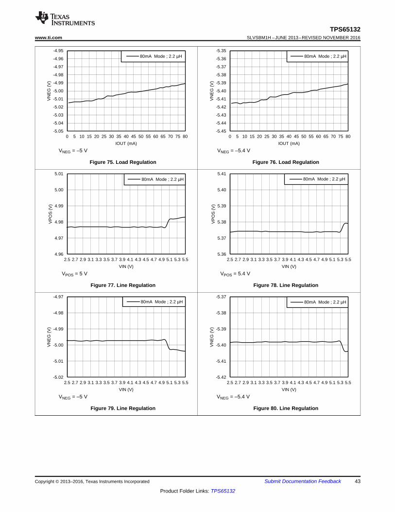
-5.02
-5.01
-5.00
-4.99
-4.98
-4.97
2.5 2.7 2.9 3.1 3.3 3.5 3.7 3.9 4.1 4.3 4.5 4.7 4.9 5.1 5.3 5.5
VN
EG
(V
)
VIN (V)
80mA Mode ; 2.2 µH
C02
-5.42
-5.41
-5.40
-5.39
-5.38
-5.37
2.5 2.7 2.9 3.1 3.3 3.5 3.7 3.9 4.1 4.3 4.5 4.7 4.9 5.1 5.3 5.5
VN
EG
(V
)
VIN (V)
80mA Mode ; 2.2 µH
C02
4.96
4.97
4.98
4.99
5.00
5.01
2.5 2.7 2.9 3.1 3.3 3.5 3.7 3.9 4.1 4.3 4.5 4.7 4.9 5.1 5.3 5.5
VP
OS
(V
)
VIN (V)
80mA Mode ; 2.2 µH
C02
5.36
5.37
5.38
5.39
5.40
5.41
2.5 2.7 2.9 3.1 3.3 3.5 3.7 3.9 4.1 4.3 4.5 4.7 4.9 5.1 5.3 5.5
VP
OS
(V
)
VIN (V)
80mA Mode ; 2.2 µH
C02
-5.05
-5.04
-5.03
-5.02
-5.01
-5.00
-4.99
-4.98
-4.97
-4.96
-4.95
0 5 10 15 20 25 30 35 40 45 50 55 60 65 70 75 80
VN
EG
(V
)
IOUT (mA)
80mA Mode ; 2.2 µH
C01
-5.45
-5.44
-5.43
-5.42
-5.41
-5.40
-5.39
-5.38
-5.37
-5.36
-5.35
0 5 10 15 20 25 30 35 40 45 50 55 60 65 70 75 80
VN
EG
(V
)
IOUT (mA)
80mA Mode ; 2.2 µH
C01
43
TPS65132www.ti.com SLVSBM1H –JUNE 2013–REVISED NOVEMBER 2016
Product Folder Links: TPS65132
Submit Documentation FeedbackCopyright © 2013–2016, Texas Instruments Incorporated
VNEG = –5 V
Figure 75. Load Regulation
VNEG = –5.4 V
Figure 76. Load Regulation
VPOS = 5 V
Figure 77. Line Regulation
VPOS = 5.4 V
Figure 78. Line Regulation
VNEG = –5 V
Figure 79. Line Regulation
VNEG = –5.4 V
Figure 80. Line Regulation
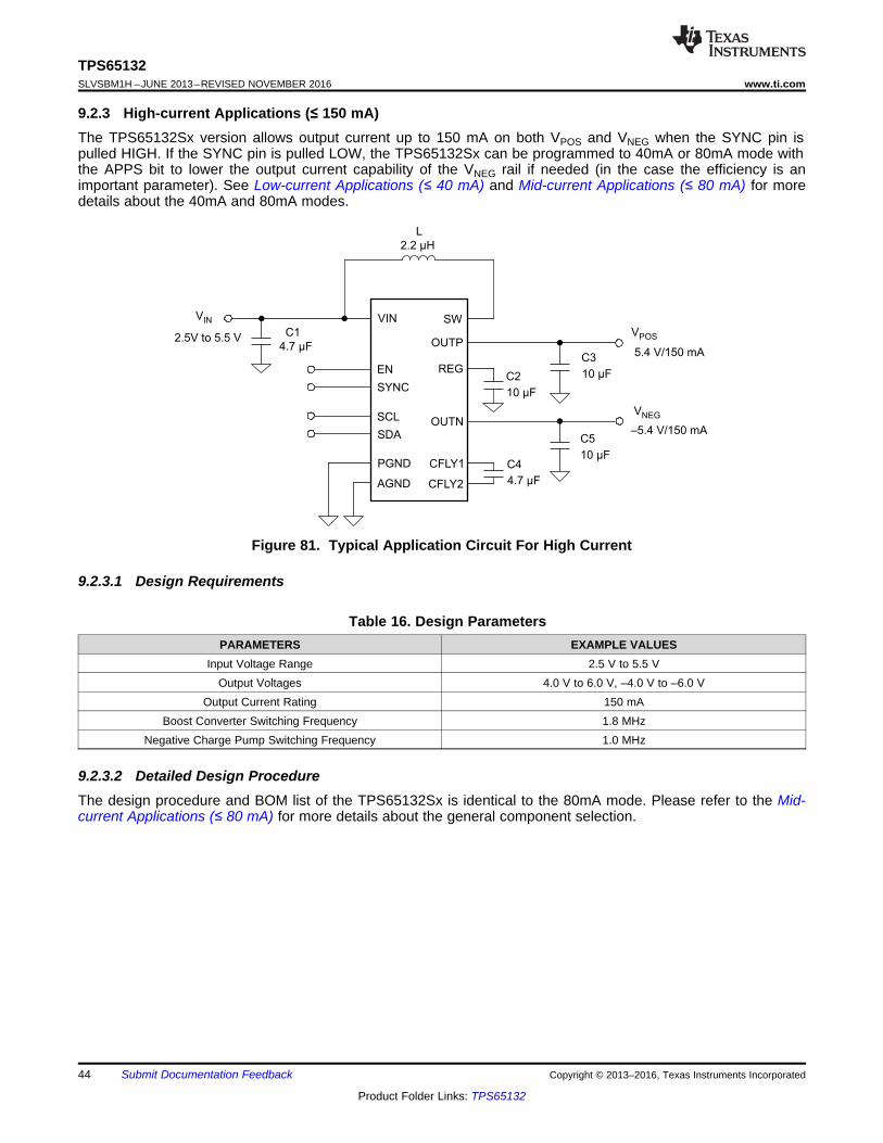
C1
C3
C2
C4
C5
4.7 µF
L
2.2 µH
EN
SYNC
OUTP
REG
SW
PGND
VIN
VPOS
VNEG
2.5V to 5.5 V
SCL
SDA
5.4 V/150 mA
OUTN
CFLY1
CFLY2
–5.4 V/150 mA
AGND
10 µF
10 µF
10 µF
4.7 µF
VIN
44
TPS65132SLVSBM1H –JUNE 2013–REVISED NOVEMBER 2016 www.ti.com
Product Folder Links: TPS65132
Submit Documentation Feedback Copyright © 2013–2016, Texas Instruments Incorporated
9.2.3 High-current Applications (≤ 150 mA)The TPS65132Sx version allows output current up to 150 mA on both VPOS and VNEG when the SYNC pin ispulled HIGH. If the SYNC pin is pulled LOW, the TPS65132Sx can be programmed to 40mA or 80mA mode withthe APPS bit to lower the output current capability of the VNEG rail if needed (in the case the efficiency is animportant parameter). See Low-current Applications (≤ 40 mA) and Mid-current Applications (≤ 80 mA) for moredetails about the 40mA and 80mA modes.
Figure 81. Typical Application Circuit For High Current
9.2.3.1 Design Requirements
Table 16. Design ParametersPARAMETERS EXAMPLE VALUES
Input Voltage Range 2.5 V to 5.5 VOutput Voltages 4.0 V to 6.0 V, –4.0 V to –6.0 V
Output Current Rating 150 mABoost Converter Switching Frequency 1.8 MHz
Negative Charge Pump Switching Frequency 1.0 MHz
9.2.3.2 Detailed Design ProcedureThe design procedure and BOM list of the TPS65132Sx is identical to the 80mA mode. Please refer to the Mid-current Applications (≤ 80 mA) for more details about the general component selection.
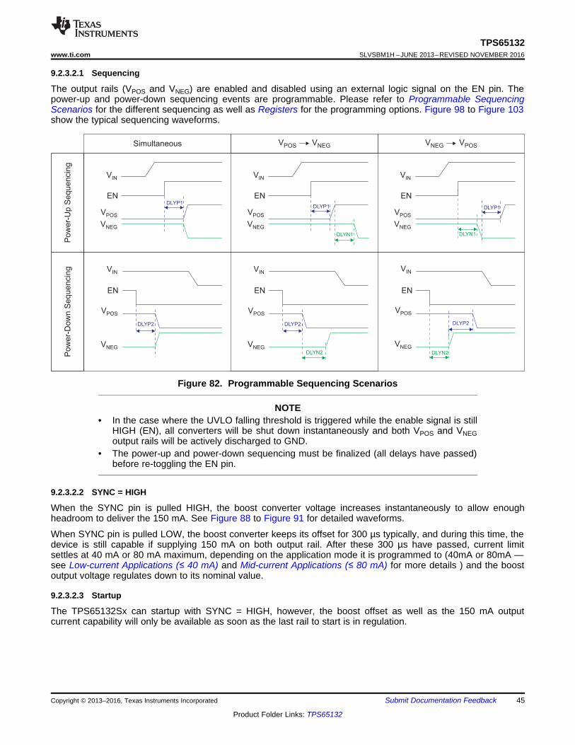
VPOS
VIN
VNEG
EN
DLYP1
DLYN1
VPOS
VIN
VNEG
DLYP1
DLYN1
EN
VPOS
VIN
VNEG
DLYP1EN
DLYN2
DLYP2
VPOS
VIN
VNEG
EN
DLYN2
DLYP2
VPOS
VIN
VNEG
EN
VPOS
VIN
VNEG
DLYP2
EN
Po
we
r-U
p S
eq
ue
ncin
gP
ow
er-
Do
wn
Se
qu
en
cin
g
Simultaneous V VPOS NEG V VNEG POS
45
TPS65132www.ti.com SLVSBM1H –JUNE 2013–REVISED NOVEMBER 2016
Product Folder Links: TPS65132
Submit Documentation FeedbackCopyright © 2013–2016, Texas Instruments Incorporated
9.2.3.2.1 Sequencing
The output rails (VPOS and VNEG) are enabled and disabled using an external logic signal on the EN pin. Thepower-up and power-down sequencing events are programmable. Please refer to Programmable SequencingScenarios for the different sequencing as well as Registers for the programming options. Figure 98 to Figure 103show the typical sequencing waveforms.
Figure 82. Programmable Sequencing Scenarios
NOTE• In the case where the UVLO falling threshold is triggered while the enable signal is still
HIGH (EN), all converters will be shut down instantaneously and both VPOS and VNEGoutput rails will be actively discharged to GND.
• The power-up and power-down sequencing must be finalized (all delays have passed)before re-toggling the EN pin.
9.2.3.2.2 SYNC = HIGH
When the SYNC pin is pulled HIGH, the boost converter voltage increases instantaneously to allow enoughheadroom to deliver the 150 mA. See Figure 88 to Figure 91 for detailed waveforms.
When SYNC pin is pulled LOW, the boost converter keeps its offset for 300 µs typically, and during this time, thedevice is still capable if supplying 150 mA on both output rail. After these 300 µs have passed, current limitsettles at 40 mA or 80 mA maximum, depending on the application mode it is programmed to (40mA or 80mA —see Low-current Applications (≤ 40 mA) and Mid-current Applications (≤ 80 mA) for more details ) and the boostoutput voltage regulates down to its nominal value.
9.2.3.2.3 Startup
The TPS65132Sx can startup with SYNC = HIGH, however, the boost offset as well as the 150 mA outputcurrent capability will only be available as soon as the last rail to start is in regulation.
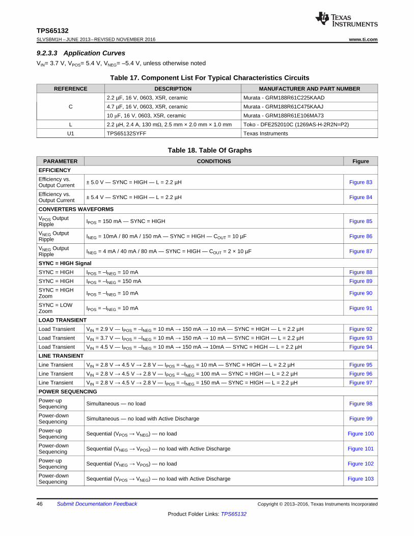
46
TPS65132SLVSBM1H –JUNE 2013–REVISED NOVEMBER 2016 www.ti.com
Product Folder Links: TPS65132
Submit Documentation Feedback Copyright © 2013–2016, Texas Instruments Incorporated
9.2.3.3 Application CurvesVIN= 3.7 V, VPOS= 5.4 V, VNEG= –5.4 V, unless otherwise noted
Table 17. Component List For Typical Characteristics CircuitsREFERENCE DESCRIPTION MANUFACTURER AND PART NUMBER
C2.2 µF, 16 V, 0603, X5R, ceramic Murata - GRM188R61C225KAAD4.7 µF, 16 V, 0603, X5R, ceramic Murata - GRM188R61C475KAAJ10 μF, 16 V, 0603, X5R, ceramic Murata - GRM188R61E106MA73
L 2.2 µH, 2.4 A, 130 mΩ, 2.5 mm × 2.0 mm × 1.0 mm Toko - DFE252010C (1269AS-H-2R2N=P2)U1 TPS65132SYFF Texas Instruments
Table 18. Table Of GraphsPARAMETER CONDITIONS Figure
EFFICIENCYEfficiency vs.Output Current ± 5.0 V — SYNC = HIGH — L = 2.2 µH Figure 83
Efficiency vs.Output Current ± 5.4 V — SYNC = HIGH — L = 2.2 µH Figure 84
CONVERTERS WAVEFORMSVPOS OutputRipple IPOS = 150 mA — SYNC = HIGH Figure 85
VNEG OutputRipple INEG = 10mA / 80 mA / 150 mA — SYNC = HIGH — COUT = 10 µF Figure 86
VNEG OutputRipple INEG = 4 mA / 40 mA / 80 mA — SYNC = HIGH — COUT = 2 × 10 µF Figure 87
SYNC = HIGH SignalSYNC = HIGH IPOS = –INEG = 10 mA Figure 88SYNC = HIGH IPOS = –INEG = 150 mA Figure 89SYNC = HIGHZoom IPOS = –INEG = 10 mA Figure 90
SYNC = LOWZoom IPOS = –INEG = 10 mA Figure 91
LOAD TRANSIENTLoad Transient VIN = 2.9 V — IPOS = –INEG = 10 mA → 150 mA → 10 mA — SYNC = HIGH — L = 2.2 µH Figure 92Load Transient VIN = 3.7 V — IPOS = –INEG = 10 mA → 150 mA → 10 mA — SYNC = HIGH — L = 2.2 µH Figure 93Load Transient VIN = 4.5 V — IPOS = –INEG = 10 mA → 150 mA → 10mA — SYNC = HIGH — L = 2.2 µH Figure 94LINE TRANSIENTLine Transient VIN = 2.8 V → 4.5 V → 2.8 V — IPOS = –INEG = 10 mA — SYNC = HIGH — L = 2.2 µH Figure 95Line Transient VIN = 2.8 V → 4.5 V → 2.8 V — IPOS = –INEG = 100 mA — SYNC = HIGH — L = 2.2 µH Figure 96Line Transient VIN = 2.8 V → 4.5 V → 2.8 V — IPOS = –INEG = 150 mA — SYNC = HIGH — L = 2.2 µH Figure 97POWER SEQUENCINGPower-upSequencing Simultaneous — no load Figure 98
Power-downSequencing Simultaneous — no load with Active Discharge Figure 99
Power-upSequencing Sequential (VPOS → VNEG) — no load Figure 100
Power-downSequencing Sequential (VNEG → VPOS) — no load with Active Discharge Figure 101
Power-upSequencing Sequential (VNEG → VPOS) — no load Figure 102
Power-downSequencing Sequential (VPOS → VNEG) — no load with Active Discharge Figure 103
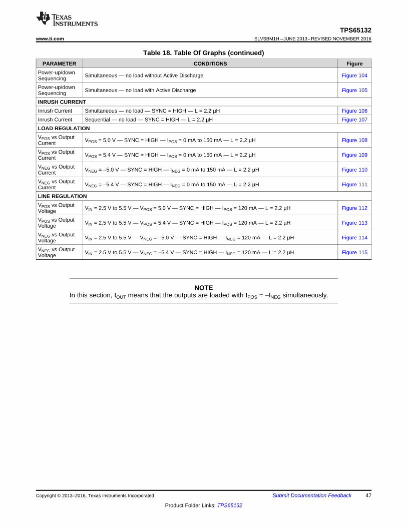
47
TPS65132www.ti.com SLVSBM1H –JUNE 2013–REVISED NOVEMBER 2016
Product Folder Links: TPS65132
Submit Documentation FeedbackCopyright © 2013–2016, Texas Instruments Incorporated
Table 18. Table Of Graphs (continued)PARAMETER CONDITIONS Figure
Power-up/downSequencing Simultaneous — no load without Active Discharge Figure 104
Power-up/downSequencing Simultaneous — no load with Active Discharge Figure 105
INRUSH CURRENTInrush Current Simultaneous — no load — SYNC = HIGH — L = 2.2 µH Figure 106Inrush Current Sequential — no load — SYNC = HIGH — L = 2.2 µH Figure 107LOAD REGULATIONVPOS vs OutputCurrent VPOS = 5.0 V — SYNC = HIGH — IPOS = 0 mA to 150 mA — L = 2.2 µH Figure 108
VPOS vs OutputCurrent VPOS = 5.4 V — SYNC = HIGH — IPOS = 0 mA to 150 mA — L = 2.2 µH Figure 109
VNEG vs OutputCurrent VNEG = –5.0 V — SYNC = HIGH — INEG = 0 mA to 150 mA — L = 2.2 µH Figure 110
VNEG vs OutputCurrent VNEG = –5.4 V — SYNC = HIGH — INEG = 0 mA to 150 mA — L = 2.2 µH Figure 111
LINE REGULATIONVPOS vs OutputVoltage VIN = 2.5 V to 5.5 V — VPOS = 5.0 V — SYNC = HIGH — IPOS = 120 mA — L = 2.2 µH Figure 112
VPOS vs OutputVoltage VIN = 2.5 V to 5.5 V — VPOS = 5.4 V — SYNC = HIGH — IPOS = 120 mA — L = 2.2 µH Figure 113
VNEG vs OutputVoltage VIN = 2.5 V to 5.5 V — VNEG = –5.0 V — SYNC = HIGH — INEG = 120 mA — L = 2.2 µH Figure 114
VNEG vs OutputVoltage VIN = 2.5 V to 5.5 V — VNEG = –5.4 V — SYNC = HIGH — INEG = 120 mA — L = 2.2 µH Figure 115
spacer
NOTEIn this section, IOUT means that the outputs are loaded with IPOS = –INEG simultaneously.
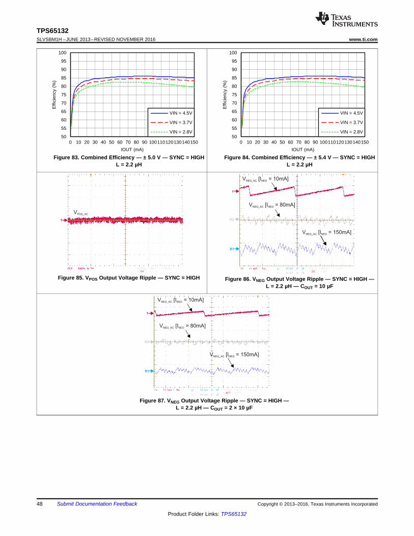
1
R1
R2
V [I = 10mA]NEG_AC NEG
V [ = 80mA]NEG_AC INEG
V [ = 150mA]NEG_AC INEG
R1
R2
50.0mV AC BW
50.0mV AC BW
1
R1
R1
R2
50.0mV AC BW
V [I = 10mA]NEG_AC NEG
V [ = 80mA]NEG_AC INEG
V [ = 150mA]NEG_AC INEG
R1
R2
50.0mV AC BW
50.0mV AC BW
1
VPOS_AC
50
55
60
65
70
75
80
85
90
95
100
0 10 20 30 40 50 60 70 80 90 100110120130140150
Effi
cien
cy (
%)
IOUT (mA)
VIN = 4.5V
VIN = 3.7V
VIN = 2.8V
C02
50
55
60
65
70
75
80
85
90
95
100
0 10 20 30 40 50 60 70 80 90 100110120130140150
Effi
cien
cy (
%)
IOUT (mA)
VIN = 4.5V
VIN = 3.7V
VIN = 2.8V
C02
48
TPS65132SLVSBM1H –JUNE 2013–REVISED NOVEMBER 2016 www.ti.com
Product Folder Links: TPS65132
Submit Documentation Feedback Copyright © 2013–2016, Texas Instruments Incorporated
Figure 83. Combined Efficiency — ± 5.0 V — SYNC = HIGHL = 2.2 µH
Figure 84. Combined Efficiency — ± 5.4 V — SYNC = HIGHL = 2.2 µH
Figure 85. VPOS Output Voltage Ripple — SYNC = HIGH Figure 86. VNEG Output Voltage Ripple — SYNC = HIGH —L = 2.2 µH — COUT = 10 µF
Figure 87. VNEG Output Voltage Ripple — SYNC = HIGH —L = 2.2 µH — COUT = 2 × 10 µF
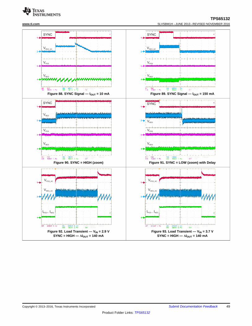
1
2
4
VNEG_AC
VPOS_AC
IPOS = - NEGI
1
2
4
VNEG_AC
VPOS_AC
IPOS = - NEGI
1
2
4
3
SYNC
VREG
VPOS
VNEG
1
2
4
3
SYNC
VREG
VPOS
VNEG
1
2
4
3
SYNC
VREG_AC
VPOS
VNEG
1
2
4
3
SYNC
VREG_AC
VPOS
VNEG
49
TPS65132www.ti.com SLVSBM1H –JUNE 2013–REVISED NOVEMBER 2016
Product Folder Links: TPS65132
Submit Documentation FeedbackCopyright © 2013–2016, Texas Instruments Incorporated
Figure 88. SYNC Signal — IOUT = 10 mA Figure 89. SYNC Signal — IOUT = 150 mA
Figure 90. SYNC = HIGH (zoom) Figure 91. SYNC = LOW (zoom) with Delay
Figure 92. Load Transient — VIN = 2.9 VSYNC = HIGH — ΔIOUT = 140 mA
Figure 93. Load Transient — VIN = 3.7 VSYNC = HIGH — ΔIOUT = 140 mA
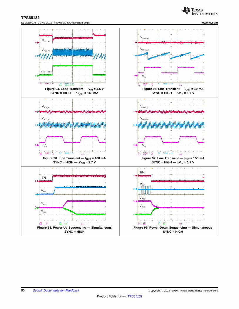
1
2
3
EN
VREG
VPOS
VNEG
4
1
2
3
EN
VSW
VPOS
VNEG
4
1
2
3
VNEG_AC
VPOS_AC
VIN
1
2
3
VNEG_AC
VPOS_AC
VIN
1
2
4
VNEG_AC
VPOS_AC
IPOS = - NEGI
1
2
3
VNEG_AC
VPOS_AC
VIN
50
TPS65132SLVSBM1H –JUNE 2013–REVISED NOVEMBER 2016 www.ti.com
Product Folder Links: TPS65132
Submit Documentation Feedback Copyright © 2013–2016, Texas Instruments Incorporated
Figure 94. Load Transient — VIN = 4.5 VSYNC = HIGH — ΔIOUT = 140 mA
Figure 95. Line Transient — IOUT = 10 mASYNC = HIGH — ΔVIN = 1.7 V
Figure 96. Line Transient — IOUT = 100 mASYNC = HIGH — ΔVIN = 1.7 V
Figure 97. Line Transient — IOUT = 150 mASYNC = HIGH — ΔVIN = 1.7 V
Figure 98. Power-Up Sequencing — SimultaneousSYNC = HIGH
Figure 99. Power-Down Sequencing — SimultaneousSYNC = HIGH
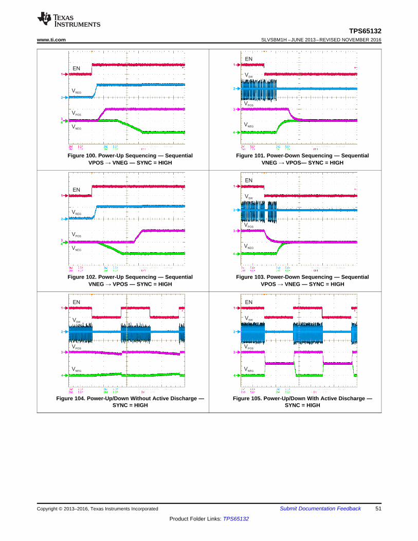
1
2
4
3
EN
VSW
VPOS
VNEG
1
2
4
3
EN
VSW
VPOS
VNEG
1
2
3
EN
VREG
VPOS
VNEG
4
1
2
3
EN
VSW
VPOS
VNEG
4
1
2
3
EN
VREG
VPOS
VNEG
4
1
2
3
EN
VSW
VPOS
VNEG
4
51
TPS65132www.ti.com SLVSBM1H –JUNE 2013–REVISED NOVEMBER 2016
Product Folder Links: TPS65132
Submit Documentation FeedbackCopyright © 2013–2016, Texas Instruments Incorporated
Figure 100. Power-Up Sequencing — SequentialVPOS → VNEG — SYNC = HIGH
Figure 101. Power-Down Sequencing — SequentialVNEG → VPOS— SYNC = HIGH
Figure 102. Power-Up Sequencing — SequentialVNEG → VPOS — SYNC = HIGH
Figure 103. Power-Down Sequencing — SequentialVPOS → VNEG — SYNC = HIGH
Figure 104. Power-Up/Down Without Active Discharge —SYNC = HIGH
Figure 105. Power-Up/Down With Active Discharge —SYNC = HIGH
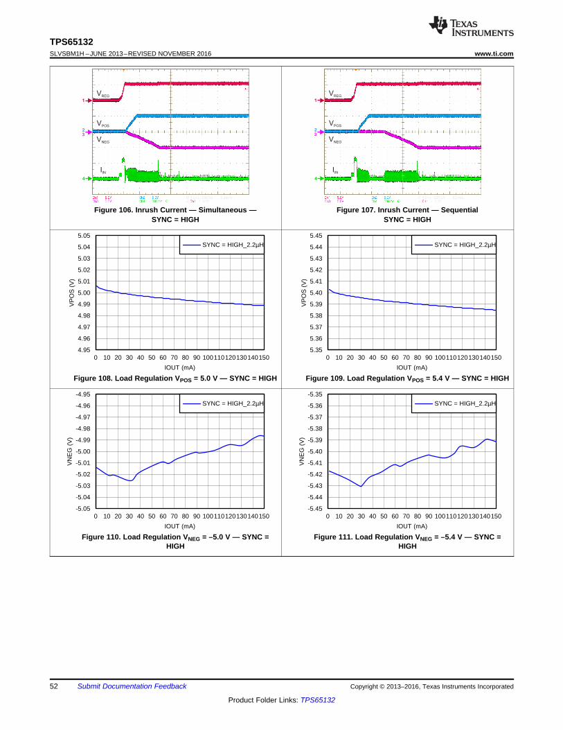
-5.05
-5.04
-5.03
-5.02
-5.01
-5.00
-4.99
-4.98
-4.97
-4.96
-4.95
0 10 20 30 40 50 60 70 80 90 100110120130140150
VN
EG
(V
)
IOUT (mA)
SYNC = HIGH_2.2µH
C02
-5.45
-5.44
-5.43
-5.42
-5.41
-5.40
-5.39
-5.38
-5.37
-5.36
-5.35
0 10 20 30 40 50 60 70 80 90 100110120130140150
VN
EG
(V
)
IOUT (mA)
SYNC = HIGH_2.2µH
C02
4.95
4.96
4.97
4.98
4.99
5.00
5.01
5.02
5.03
5.04
5.05
0 10 20 30 40 50 60 70 80 90 100110120130140150
VP
OS
(V
)
IOUT (mA)
SYNC = HIGH_2.2µH
C02
5.35
5.36
5.37
5.38
5.39
5.40
5.41
5.42
5.43
5.44
5.45
0 10 20 30 40 50 60 70 80 90 100110120130140150
VP
OS
(V
)
IOUT (mA)
SYNC = HIGH_2.2µH
C02
1
2
4
3
VREG
VPOS
VNEG
IIN
1
2
4
3
VREG
VPOS
VNEG
IIN
52
TPS65132SLVSBM1H –JUNE 2013–REVISED NOVEMBER 2016 www.ti.com
Product Folder Links: TPS65132
Submit Documentation Feedback Copyright © 2013–2016, Texas Instruments Incorporated
Figure 106. Inrush Current — Simultaneous —SYNC = HIGH
Figure 107. Inrush Current — SequentialSYNC = HIGH
Figure 108. Load Regulation VPOS = 5.0 V — SYNC = HIGH Figure 109. Load Regulation VPOS = 5.4 V — SYNC = HIGH
Figure 110. Load Regulation VNEG = –5.0 V — SYNC =HIGH
Figure 111. Load Regulation VNEG = –5.4 V — SYNC =HIGH
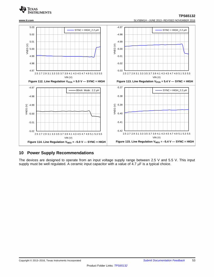
-5.02
-5.01
-5.00
-4.99
-4.98
-4.97
2.5 2.7 2.9 3.1 3.3 3.5 3.7 3.9 4.1 4.3 4.5 4.7 4.9 5.1 5.3 5.5
VN
EG
(V
)
VIN (V)
80mA Mode ; 2.2 µH
C02
-5.42
-5.41
-5.40
-5.39
-5.38
-5.37
2.5 2.7 2.9 3.1 3.3 3.5 3.7 3.9 4.1 4.3 4.5 4.7 4.9 5.1 5.3 5.5
VN
EG
(V
)
VIN (V)
SYNC = HIGH_2.2 µH
C03
4.97
4.98
4.99
5.00
5.01
5.02
5.03
2.5 2.7 2.9 3.1 3.3 3.5 3.7 3.9 4.1 4.3 4.5 4.7 4.9 5.1 5.3 5.5
VN
EG
(V
)
VIN (V)
SYNC = HIGH_2.2 µH
C03
-5.03
-5.02
-5.01
-5.00
-4.99
-4.98
-4.97
2.5 2.7 2.9 3.1 3.3 3.5 3.7 3.9 4.1 4.3 4.5 4.7 4.9 5.1 5.3 5.5
VN
EG
(V
)
VIN (V)
SYNC = HIGH_2.2 µH
C03
53
TPS65132www.ti.com SLVSBM1H –JUNE 2013–REVISED NOVEMBER 2016
Product Folder Links: TPS65132
Submit Documentation FeedbackCopyright © 2013–2016, Texas Instruments Incorporated
Figure 112. Line Regulation VPOS = 5.0 V — SYNC = HIGH Figure 113. Line Regulation VPOS = 5.4 V — SYNC = HIGH
Figure 114. Line Regulation VNEG = –5.0 V — SYNC = HIGH Figure 115. Line Regulation VNEG = –5.4 V — SYNC = HIGH
10 Power Supply RecommendationsThe devices are designed to operate from an input voltage supply range between 2.5 V and 5.5 V. This inputsupply must be well regulated. A ceramic input capacitor with a value of 4.7 μF is a typical choice.
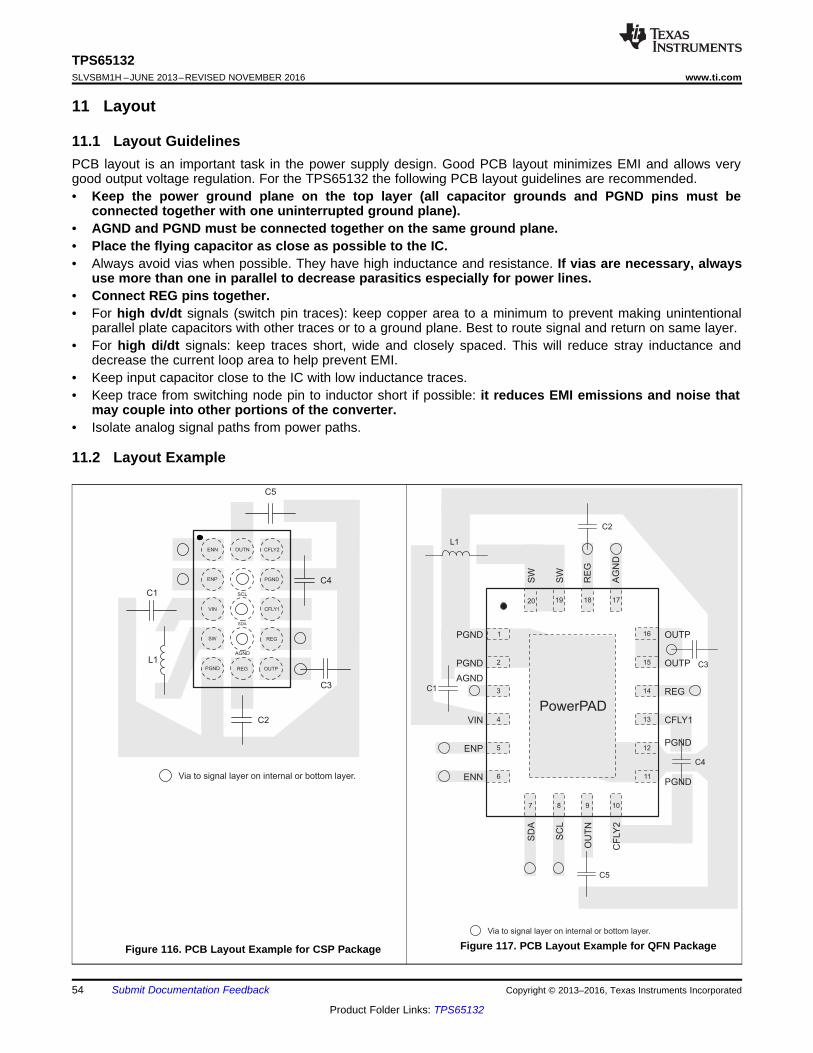
C1
L1
C2
Via to signal layer on internal or bottom layer.
PowerPAD
1 16
7
20
8
19
9
18
10
17
2 15
3 14
4 13
5 12
6 11
PGND OUTP
SW
PGND OUTP
SW
AGND
SD
A
REG
RE
G
VIN
SC
L
CFLY1
AG
ND
ENP
OU
TN
PGND
ENN
CF
LY
2
PGND
C3
C5
C4
SCL
CFLY1
SDA
REG
OUTP
AGND
REG
OUTN CFLY2
PGNDENP
VIN
SW
PGND
ENN
C1
C5
C4
L1
C3
C2
Via to signal layer on internal or bottom layer.
54
TPS65132SLVSBM1H –JUNE 2013–REVISED NOVEMBER 2016 www.ti.com
Product Folder Links: TPS65132
Submit Documentation Feedback Copyright © 2013–2016, Texas Instruments Incorporated
11 Layout
11.1 Layout GuidelinesPCB layout is an important task in the power supply design. Good PCB layout minimizes EMI and allows verygood output voltage regulation. For the TPS65132 the following PCB layout guidelines are recommended.• Keep the power ground plane on the top layer (all capacitor grounds and PGND pins must be
connected together with one uninterrupted ground plane).• AGND and PGND must be connected together on the same ground plane.• Place the flying capacitor as close as possible to the IC.• Always avoid vias when possible. They have high inductance and resistance. If vias are necessary, always
use more than one in parallel to decrease parasitics especially for power lines.• Connect REG pins together.• For high dv/dt signals (switch pin traces): keep copper area to a minimum to prevent making unintentional
parallel plate capacitors with other traces or to a ground plane. Best to route signal and return on same layer.• For high di/dt signals: keep traces short, wide and closely spaced. This will reduce stray inductance and
decrease the current loop area to help prevent EMI.• Keep input capacitor close to the IC with low inductance traces.• Keep trace from switching node pin to inductor short if possible: it reduces EMI emissions and noise that
may couple into other portions of the converter.• Isolate analog signal paths from power paths.
11.2 Layout Example
Figure 116. PCB Layout Example for CSP Package Figure 117. PCB Layout Example for QFN Package
55
TPS65132www.ti.com SLVSBM1H –JUNE 2013–REVISED NOVEMBER 2016
Product Folder Links: TPS65132
Submit Documentation FeedbackCopyright © 2013–2016, Texas Instruments Incorporated
12 Device and Documentation Support
12.1 Device Support
12.1.1 Third-Party Products DisclaimerTI'S PUBLICATION OF INFORMATION REGARDING THIRD-PARTY PRODUCTS OR SERVICES DOES NOTCONSTITUTE AN ENDORSEMENT REGARDING THE SUITABILITY OF SUCH PRODUCTS OR SERVICESOR A WARRANTY, REPRESENTATION OR ENDORSEMENT OF SUCH PRODUCTS OR SERVICES, EITHERALONE OR IN COMBINATION WITH ANY TI PRODUCT OR SERVICE.
12.2 Receiving Notification of Documentation UpdatesTo receive notification of documentation updates, navigate to the device product folder on ti.com. In the upperright corner, click on Alert me to register and receive a weekly digest of any product information that haschanged. For change details, review the revision history included in any revised document.
12.3 Community ResourcesThe following links connect to TI community resources. Linked contents are provided "AS IS" by the respectivecontributors. They do not constitute TI specifications and do not necessarily reflect TI's views; see TI's Terms ofUse.
TI E2E™ Online Community TI's Engineer-to-Engineer (E2E) Community. Created to foster collaborationamong engineers. At e2e.ti.com, you can ask questions, share knowledge, explore ideas and helpsolve problems with fellow engineers.
Design Support TI's Design Support Quickly find helpful E2E forums along with design support tools andcontact information for technical support.
12.4 TrademarksE2E is a trademark of Texas Instruments.All other trademarks are the property of their respective owners.
12.5 Electrostatic Discharge CautionThese devices have limited built-in ESD protection. The leads should be shorted together or the device placed in conductive foamduring storage or handling to prevent electrostatic damage to the MOS gates.
12.6 GlossarySLYZ022 — TI Glossary.
This glossary lists and explains terms, acronyms, and definitions.
13 Mechanical, Packaging, and Orderable InformationThe following pages include mechanical packaging and orderable information. This information is the mostcurrent data available for the designated devices. This data is subject to change without notice and revision ofthis document. For browser-based versions of this data sheet, refer to the left-hand navigation.
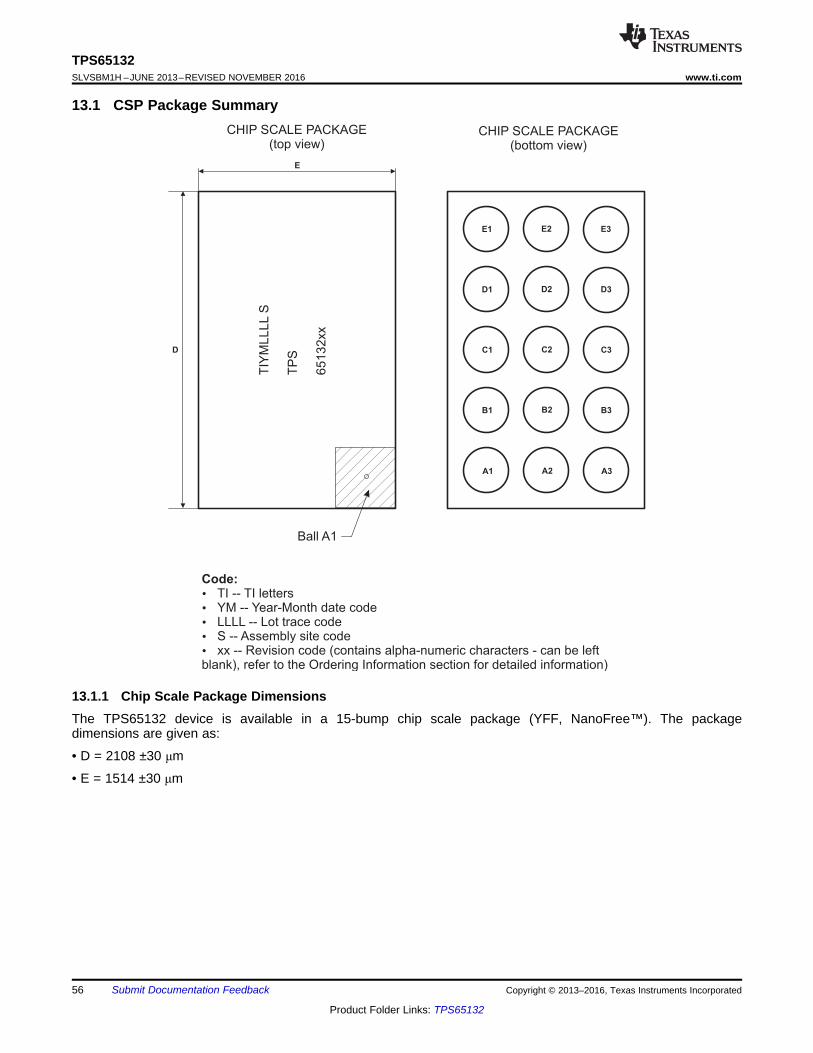
A2
B2
C2
D2
E2
A3
B3
C3
D3
E3
A1
B1
C1
D1
E1
D
E
Ball A1
CHIP SCALE PACKAGE(bottom view)
CHIP SCALE PACKAGE(top view)
Code:
�
�
�
�
TI -- TI letters
LLLL -- Lot trace codeS -- Assembly site code
� YM -- Year-Month date code
xx -- Revision code (contains alpha-numeric characters - can be leftblank), refer to the Ordering Information section for detailed information)
TIY
MLLLL
S
TP
S
65132xx
56
TPS65132SLVSBM1H –JUNE 2013–REVISED NOVEMBER 2016 www.ti.com
Product Folder Links: TPS65132
Submit Documentation Feedback Copyright © 2013–2016, Texas Instruments Incorporated
13.1 CSP Package Summary
13.1.1 Chip Scale Package DimensionsThe TPS65132 device is available in a 15-bump chip scale package (YFF, NanoFree™). The packagedimensions are given as:
• D = 2108 ±30 μm
• E = 1514 ±30 μm
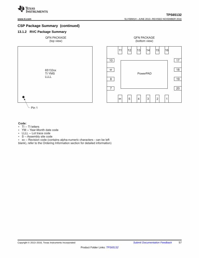
Pin 1
QFN PACKAGE(bottom view)
QFN PACKAGE(top view)
65132xxTI YMSLLLL
1
16
7 20
8 19
9
18
10 17
2
15
3
14
4
13
5
12
6
11
PowerPAD
Code:
�
�
�
�
TI -- TI letters
LLLL -- Lot trace codeS -- Assembly site code
� YM -- Year-Month date code
xx -- Revision code (contains alpha-numeric characters - can be leftblank), refer to the Ordering Information section for detailed information)
57
TPS65132www.ti.com SLVSBM1H –JUNE 2013–REVISED NOVEMBER 2016
Product Folder Links: TPS65132
Submit Documentation FeedbackCopyright © 2013–2016, Texas Instruments Incorporated
CSP Package Summary (continued)13.1.2 RVC Package Summary
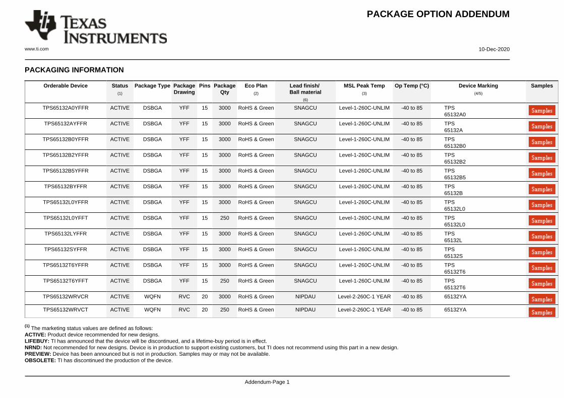
PACKAGE OPTION ADDENDUM
www.ti.com 10-Dec-2020
Addendum-Page 1
PACKAGING INFORMATION
Orderable Device Status(1)
Package Type PackageDrawing
Pins PackageQty
Eco Plan(2)
Lead finish/Ball material
(6)
MSL Peak Temp(3)
Op Temp (°C) Device Marking(4/5)
Samples
TPS65132A0YFFR ACTIVE DSBGA YFF 15 3000 RoHS & Green SNAGCU Level-1-260C-UNLIM -40 to 85 TPS65132A0
TPS65132AYFFR ACTIVE DSBGA YFF 15 3000 RoHS & Green SNAGCU Level-1-260C-UNLIM -40 to 85 TPS65132A
TPS65132B0YFFR ACTIVE DSBGA YFF 15 3000 RoHS & Green SNAGCU Level-1-260C-UNLIM -40 to 85 TPS65132B0
TPS65132B2YFFR ACTIVE DSBGA YFF 15 3000 RoHS & Green SNAGCU Level-1-260C-UNLIM -40 to 85 TPS65132B2
TPS65132B5YFFR ACTIVE DSBGA YFF 15 3000 RoHS & Green SNAGCU Level-1-260C-UNLIM -40 to 85 TPS65132B5
TPS65132BYFFR ACTIVE DSBGA YFF 15 3000 RoHS & Green SNAGCU Level-1-260C-UNLIM -40 to 85 TPS65132B
TPS65132L0YFFR ACTIVE DSBGA YFF 15 3000 RoHS & Green SNAGCU Level-1-260C-UNLIM -40 to 85 TPS65132L0
TPS65132L0YFFT ACTIVE DSBGA YFF 15 250 RoHS & Green SNAGCU Level-1-260C-UNLIM -40 to 85 TPS65132L0
TPS65132LYFFR ACTIVE DSBGA YFF 15 3000 RoHS & Green SNAGCU Level-1-260C-UNLIM -40 to 85 TPS65132L
TPS65132SYFFR ACTIVE DSBGA YFF 15 3000 RoHS & Green SNAGCU Level-1-260C-UNLIM -40 to 85 TPS65132S
TPS65132T6YFFR ACTIVE DSBGA YFF 15 3000 RoHS & Green SNAGCU Level-1-260C-UNLIM -40 to 85 TPS65132T6
TPS65132T6YFFT ACTIVE DSBGA YFF 15 250 RoHS & Green SNAGCU Level-1-260C-UNLIM -40 to 85 TPS65132T6
TPS65132WRVCR ACTIVE WQFN RVC 20 3000 RoHS & Green NIPDAU Level-2-260C-1 YEAR -40 to 85 65132YA
TPS65132WRVCT ACTIVE WQFN RVC 20 250 RoHS & Green NIPDAU Level-2-260C-1 YEAR -40 to 85 65132YA
(1) The marketing status values are defined as follows:ACTIVE: Product device recommended for new designs.LIFEBUY: TI has announced that the device will be discontinued, and a lifetime-buy period is in effect.NRND: Not recommended for new designs. Device is in production to support existing customers, but TI does not recommend using this part in a new design.PREVIEW: Device has been announced but is not in production. Samples may or may not be available.OBSOLETE: TI has discontinued the production of the device.
PACKAGE OPTION ADDENDUM
www.ti.com 10-Dec-2020
Addendum-Page 2
(2) RoHS: TI defines "RoHS" to mean semiconductor products that are compliant with the current EU RoHS requirements for all 10 RoHS substances, including the requirement that RoHS substancedo not exceed 0.1% by weight in homogeneous materials. Where designed to be soldered at high temperatures, "RoHS" products are suitable for use in specified lead-free processes. TI mayreference these types of products as "Pb-Free".RoHS Exempt: TI defines "RoHS Exempt" to mean products that contain lead but are compliant with EU RoHS pursuant to a specific EU RoHS exemption.Green: TI defines "Green" to mean the content of Chlorine (Cl) and Bromine (Br) based flame retardants meet JS709B low halogen requirements of <=1000ppm threshold. Antimony trioxide basedflame retardants must also meet the <=1000ppm threshold requirement.
(3) MSL, Peak Temp. - The Moisture Sensitivity Level rating according to the JEDEC industry standard classifications, and peak solder temperature.
(4) There may be additional marking, which relates to the logo, the lot trace code information, or the environmental category on the device.
(5) Multiple Device Markings will be inside parentheses. Only one Device Marking contained in parentheses and separated by a "~" will appear on a device. If a line is indented then it is a continuationof the previous line and the two combined represent the entire Device Marking for that device.
(6) Lead finish/Ball material - Orderable Devices may have multiple material finish options. Finish options are separated by a vertical ruled line. Lead finish/Ball material values may wrap to twolines if the finish value exceeds the maximum column width.
Important Information and Disclaimer:The information provided on this page represents TI's knowledge and belief as of the date that it is provided. TI bases its knowledge and belief on informationprovided by third parties, and makes no representation or warranty as to the accuracy of such information. Efforts are underway to better integrate information from third parties. TI has taken andcontinues to take reasonable steps to provide representative and accurate information but may not have conducted destructive testing or chemical analysis on incoming materials and chemicals.TI and TI suppliers consider certain information to be proprietary, and thus CAS numbers and other limited information may not be available for release.
In no event shall TI's liability arising out of such information exceed the total purchase price of the TI part(s) at issue in this document sold by TI to Customer on an annual basis.
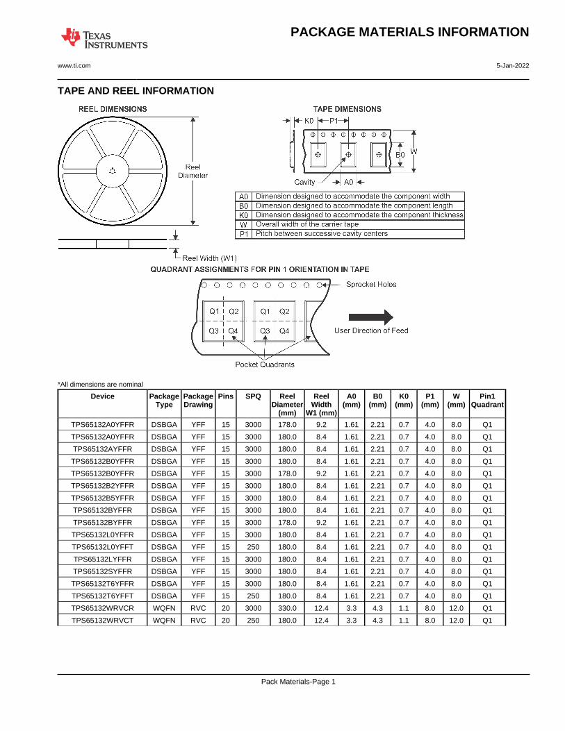
TAPE AND REEL INFORMATION
*All dimensions are nominal
Device PackageType
PackageDrawing
Pins SPQ ReelDiameter
(mm)
ReelWidth
W1 (mm)
A0(mm)
B0(mm)
K0(mm)
P1(mm)
W(mm)
Pin1Quadrant
TPS65132A0YFFR DSBGA YFF 15 3000 178.0 9.2 1.61 2.21 0.7 4.0 8.0 Q1
TPS65132A0YFFR DSBGA YFF 15 3000 180.0 8.4 1.61 2.21 0.7 4.0 8.0 Q1
TPS65132AYFFR DSBGA YFF 15 3000 180.0 8.4 1.61 2.21 0.7 4.0 8.0 Q1
TPS65132B0YFFR DSBGA YFF 15 3000 180.0 8.4 1.61 2.21 0.7 4.0 8.0 Q1
TPS65132B0YFFR DSBGA YFF 15 3000 178.0 9.2 1.61 2.21 0.7 4.0 8.0 Q1
TPS65132B2YFFR DSBGA YFF 15 3000 180.0 8.4 1.61 2.21 0.7 4.0 8.0 Q1
TPS65132B5YFFR DSBGA YFF 15 3000 180.0 8.4 1.61 2.21 0.7 4.0 8.0 Q1
TPS65132BYFFR DSBGA YFF 15 3000 180.0 8.4 1.61 2.21 0.7 4.0 8.0 Q1
TPS65132BYFFR DSBGA YFF 15 3000 178.0 9.2 1.61 2.21 0.7 4.0 8.0 Q1
TPS65132L0YFFR DSBGA YFF 15 3000 180.0 8.4 1.61 2.21 0.7 4.0 8.0 Q1
TPS65132L0YFFT DSBGA YFF 15 250 180.0 8.4 1.61 2.21 0.7 4.0 8.0 Q1
TPS65132LYFFR DSBGA YFF 15 3000 180.0 8.4 1.61 2.21 0.7 4.0 8.0 Q1
TPS65132SYFFR DSBGA YFF 15 3000 180.0 8.4 1.61 2.21 0.7 4.0 8.0 Q1
TPS65132T6YFFR DSBGA YFF 15 3000 180.0 8.4 1.61 2.21 0.7 4.0 8.0 Q1
TPS65132T6YFFT DSBGA YFF 15 250 180.0 8.4 1.61 2.21 0.7 4.0 8.0 Q1
TPS65132WRVCR WQFN RVC 20 3000 330.0 12.4 3.3 4.3 1.1 8.0 12.0 Q1
TPS65132WRVCT WQFN RVC 20 250 180.0 12.4 3.3 4.3 1.1 8.0 12.0 Q1
PACKAGE MATERIALS INFORMATION
www.ti.com 5-Jan-2022
Pack Materials-Page 1
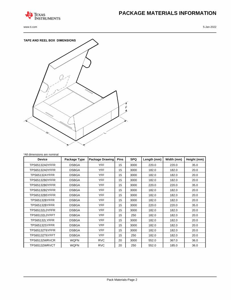
*All dimensions are nominal
Device Package Type Package Drawing Pins SPQ Length (mm) Width (mm) Height (mm)
TPS65132A0YFFR DSBGA YFF 15 3000 220.0 220.0 35.0
TPS65132A0YFFR DSBGA YFF 15 3000 182.0 182.0 20.0
TPS65132AYFFR DSBGA YFF 15 3000 182.0 182.0 20.0
TPS65132B0YFFR DSBGA YFF 15 3000 182.0 182.0 20.0
TPS65132B0YFFR DSBGA YFF 15 3000 220.0 220.0 35.0
TPS65132B2YFFR DSBGA YFF 15 3000 182.0 182.0 20.0
TPS65132B5YFFR DSBGA YFF 15 3000 182.0 182.0 20.0
TPS65132BYFFR DSBGA YFF 15 3000 182.0 182.0 20.0
TPS65132BYFFR DSBGA YFF 15 3000 220.0 220.0 35.0
TPS65132L0YFFR DSBGA YFF 15 3000 182.0 182.0 20.0
TPS65132L0YFFT DSBGA YFF 15 250 182.0 182.0 20.0
TPS65132LYFFR DSBGA YFF 15 3000 182.0 182.0 20.0
TPS65132SYFFR DSBGA YFF 15 3000 182.0 182.0 20.0
TPS65132T6YFFR DSBGA YFF 15 3000 182.0 182.0 20.0
TPS65132T6YFFT DSBGA YFF 15 250 182.0 182.0 20.0
TPS65132WRVCR WQFN RVC 20 3000 552.0 367.0 36.0
TPS65132WRVCT WQFN RVC 20 250 552.0 185.0 36.0
PACKAGE MATERIALS INFORMATION
www.ti.com 5-Jan-2022
Pack Materials-Page 2
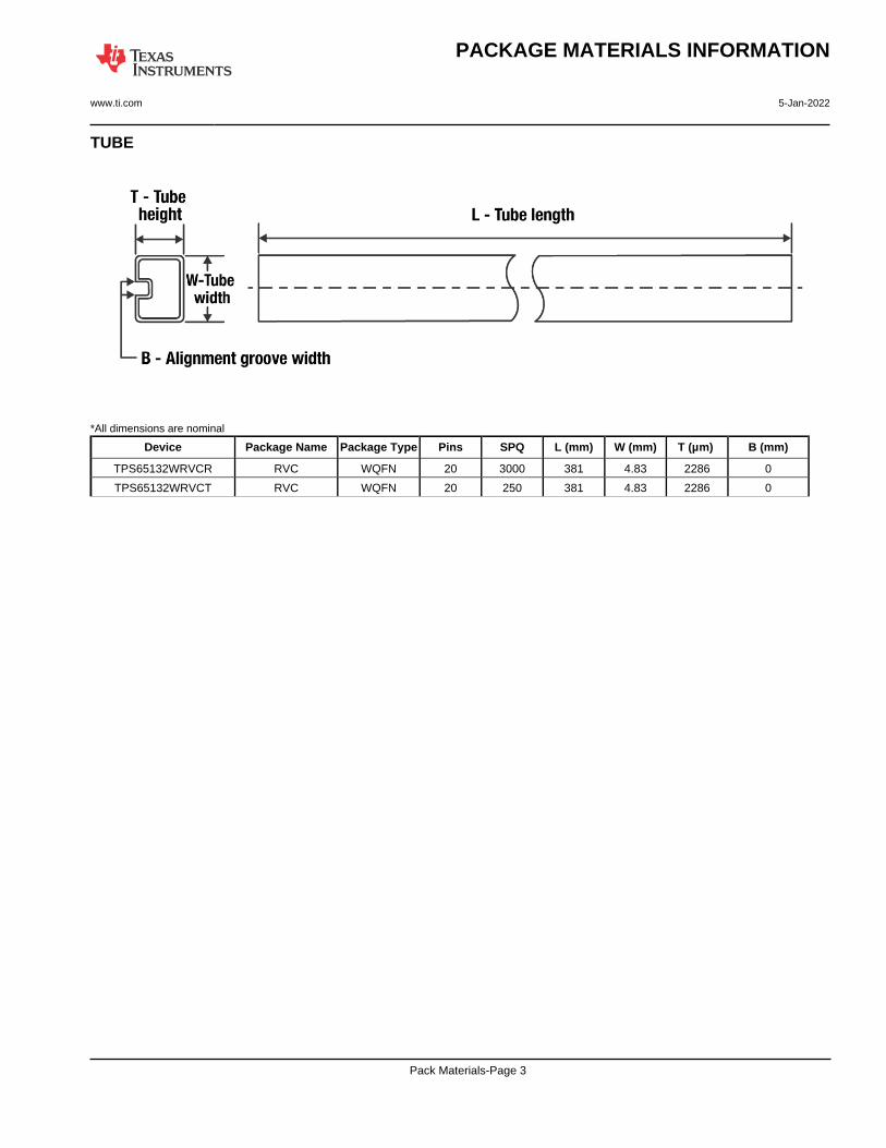
TUBE
*All dimensions are nominal
Device Package Name Package Type Pins SPQ L (mm) W (mm) T (µm) B (mm)
TPS65132WRVCR RVC WQFN 20 3000 381 4.83 2286 0
TPS65132WRVCT RVC WQFN 20 250 381 4.83 2286 0
PACKAGE MATERIALS INFORMATION
www.ti.com 5-Jan-2022
Pack Materials-Page 3
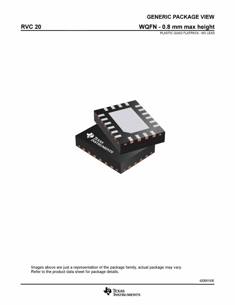
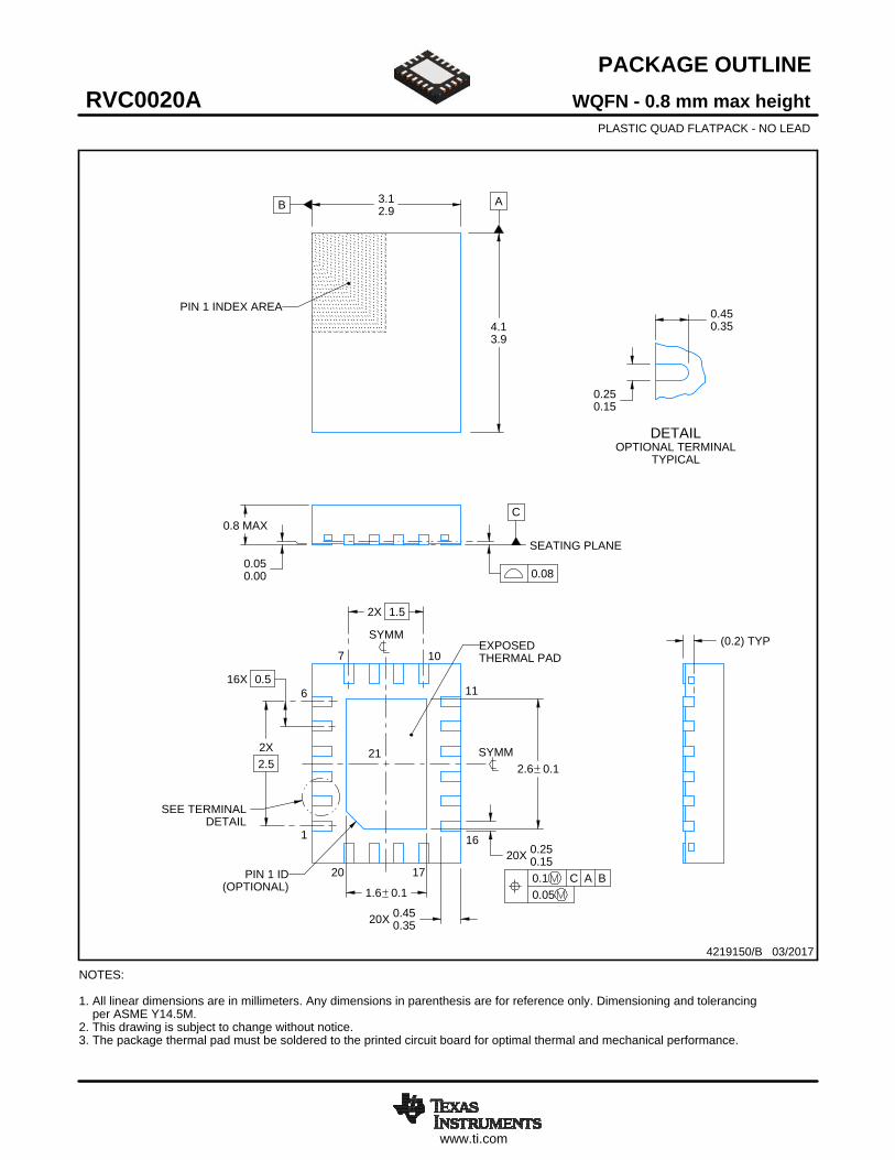
www.ti.com
PACKAGE OUTLINE
C
SEE TERMINALDETAIL
20X 0.250.15
1.6 0.1
20X 0.450.35
0.8 MAX
(0.2) TYP
0.050.00
16X 0.5
2X2.5
2X 1.5
2.6 0.1
B 3.12.9
A
4.13.9
0.250.15
0.450.35
WQFN - 0.8 mm max heightRVC0020APLASTIC QUAD FLATPACK - NO LEAD
4219150/B 03/2017
PIN 1 INDEX AREA
0.08
SEATING PLANE
1
6 11
16
7 10
20 17(OPTIONAL)
PIN 1 ID 0.1 C A B0.05
EXPOSEDTHERMAL PAD
21 SYMM
SYMM
NOTES: 1. All linear dimensions are in millimeters. Any dimensions in parenthesis are for reference only. Dimensioning and tolerancing per ASME Y14.5M. 2. This drawing is subject to change without notice. 3. The package thermal pad must be soldered to the printed circuit board for optimal thermal and mechanical performance.
SCALE 3.700
DETAILOPTIONAL TERMINAL
TYPICAL
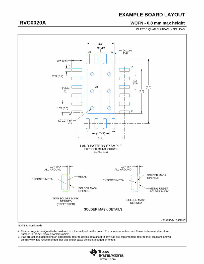
www.ti.com
EXAMPLE BOARD LAYOUT
0.07 MINALL AROUND
0.07 MAXALL AROUND
20X (0.2)
20X (0.6)
( 0.2) TYPVIA
16X (0.5)
(3.8)
(2.8)
(1)TYP
(1.6)
(R0.05)TYP
(2.6)
(1 TYP)
WQFN - 0.8 mm max heightRVC0020APLASTIC QUAD FLATPACK - NO LEAD
4219150/B 03/2017
SYMM
1
6
7 10
11
16
1720
SYMM
LAND PATTERN EXAMPLEEXPOSED METAL SHOWN
SCALE:18X
21
NOTES: (continued) 4. This package is designed to be soldered to a thermal pad on the board. For more information, see Texas Instruments literature number SLUA271 (www.ti.com/lit/slua271).5. Vias are optional depending on application, refer to device data sheet. If any vias are implemented, refer to their locations shown on this view. It is recommended that vias under paste be filled, plugged or tented.
SOLDER MASKOPENING
METAL UNDERSOLDER MASK
SOLDER MASKDEFINED
EXPOSED METALMETAL
SOLDER MASKOPENING
SOLDER MASK DETAILS
NON SOLDER MASKDEFINED
(PREFERRED)
EXPOSED METAL
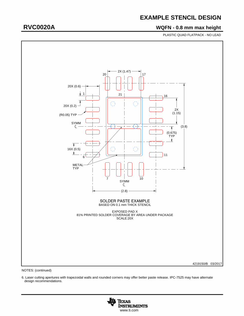
www.ti.com
EXAMPLE STENCIL DESIGN
20X (0.6)
20X (0.2)
16X (0.5)
(2.8)
(3.8)
2X (1.47)
(0.675)TYP
(R0.05) TYP2X
(1.15)
WQFN - 0.8 mm max heightRVC0020APLASTIC QUAD FLATPACK - NO LEAD
4219150/B 03/2017
NOTES: (continued) 6. Laser cutting apertures with trapezoidal walls and rounded corners may offer better paste release. IPC-7525 may have alternate design recommendations.
SYMM
METALTYP
SOLDER PASTE EXAMPLEBASED ON 0.1 mm THICK STENCIL
EXPOSED PAD X
81% PRINTED SOLDER COVERAGE BY AREA UNDER PACKAGESCALE:20X
SYMM
1
6
7 10
11
16
1720
21
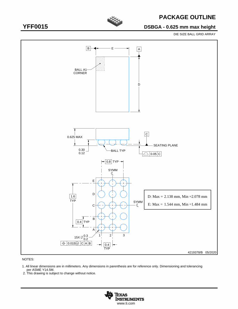
www.ti.com
PACKAGE OUTLINE
C0.625 MAX
0.300.12
1.6TYP
0.8 TYP
0.4 TYP
0.4TYP
15X 0.30.2
B E A
D
4219378/B 05/2020
DSBGA - 0.625 mm max heightYFF0015DIE SIZE BALL GRID ARRAY
NOTES: 1. All linear dimensions are in millimeters. Any dimensions in parenthesis are for reference only. Dimensioning and tolerancing per ASME Y14.5M. 2. This drawing is subject to change without notice.
BALL A1CORNER
SEATING PLANE
BALL TYP0.05 C
A
B
C
1 2 3
0.015 C A B
SYMM
SYMM
D
E
SCALE 6.000
D: Max =
E: Max =
2.138 mm, Min =
1.544 mm, Min =
2.078 mm
1.484 mm
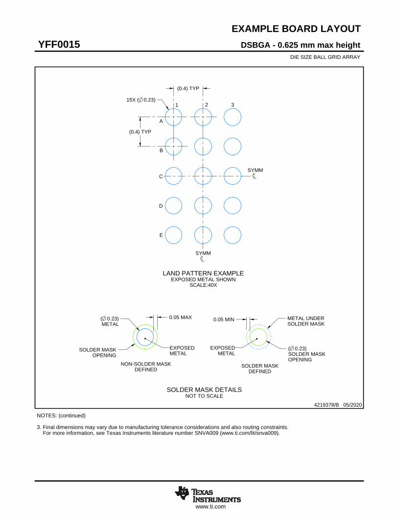
www.ti.com
EXAMPLE BOARD LAYOUT
15X ( 0.23)
(0.4) TYP
(0.4) TYP
( 0.23)METAL
0.05 MAX
SOLDER MASKOPENING
METAL UNDERSOLDER MASK
( 0.23)SOLDER MASKOPENING
0.05 MIN
4219378/B 05/2020
DSBGA - 0.625 mm max heightYFF0015DIE SIZE BALL GRID ARRAY
NOTES: (continued) 3. Final dimensions may vary due to manufacturing tolerance considerations and also routing constraints. For more information, see Texas Instruments literature number SNVA009 (www.ti.com/lit/snva009).
SOLDER MASK DETAILSNOT TO SCALE
SYMM
SYMM
LAND PATTERN EXAMPLEEXPOSED METAL SHOWN
SCALE:40X
A
B
C
1 2 3
D
E
NON-SOLDER MASKDEFINED
EXPOSEDMETAL
SOLDER MASKDEFINED
EXPOSEDMETAL
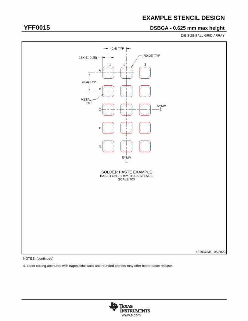
www.ti.com
EXAMPLE STENCIL DESIGN
(0.4) TYP
(0.4) TYP
15X ( 0.25) (R0.05) TYP
METALTYP
4219378/B 05/2020
DSBGA - 0.625 mm max heightYFF0015DIE SIZE BALL GRID ARRAY
NOTES: (continued) 4. Laser cutting apertures with trapezoidal walls and rounded corners may offer better paste release.
D
E
SYMM
SYMM
SOLDER PASTE EXAMPLEBASED ON 0.1 mm THICK STENCIL
SCALE:40X
A
B
C
1 2 3
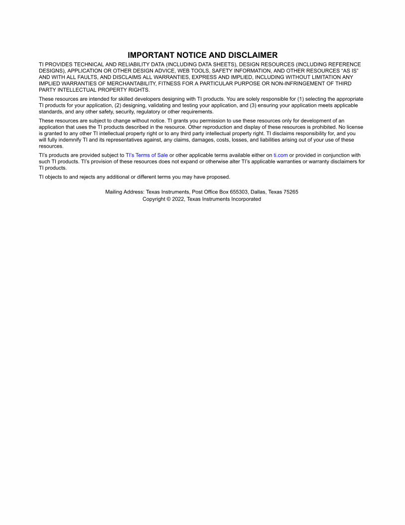
IMPORTANT NOTICE AND DISCLAIMERTI PROVIDES TECHNICAL AND RELIABILITY DATA (INCLUDING DATA SHEETS), DESIGN RESOURCES (INCLUDING REFERENCE DESIGNS), APPLICATION OR OTHER DESIGN ADVICE, WEB TOOLS, SAFETY INFORMATION, AND OTHER RESOURCES “AS IS” AND WITH ALL FAULTS, AND DISCLAIMS ALL WARRANTIES, EXPRESS AND IMPLIED, INCLUDING WITHOUT LIMITATION ANY IMPLIED WARRANTIES OF MERCHANTABILITY, FITNESS FOR A PARTICULAR PURPOSE OR NON-INFRINGEMENT OF THIRD PARTY INTELLECTUAL PROPERTY RIGHTS.These resources are intended for skilled developers designing with TI products. You are solely responsible for (1) selecting the appropriate TI products for your application, (2) designing, validating and testing your application, and (3) ensuring your application meets applicable standards, and any other safety, security, regulatory or other requirements.These resources are subject to change without notice. TI grants you permission to use these resources only for development of an application that uses the TI products described in the resource. Other reproduction and display of these resources is prohibited. No license is granted to any other TI intellectual property right or to any third party intellectual property right. TI disclaims responsibility for, and you will fully indemnify TI and its representatives against, any claims, damages, costs, losses, and liabilities arising out of your use of these resources.TI’s products are provided subject to TI’s Terms of Sale or other applicable terms available either on ti.com or provided in conjunction with such TI products. TI’s provision of these resources does not expand or otherwise alter TI’s applicable warranties or warranty disclaimers for TI products.TI objects to and rejects any additional or different terms you may have proposed. IMPORTANT NOTICE
Mailing Address: Texas Instruments, Post Office Box 655303, Dallas, Texas 75265Copyright © 2022, Texas Instruments Incorporated
Related Documents


