Topology Optimized Multi-layered Meta-optics Zin Lin 1 , * Benedikt Groever 1 , Federico Capasso 1 , Alejandro W. Rodriguez 2 , and Marko Lonˇ car 1 1 John A. Paulson School of Engineering and Applied Sciences, Harvard University, Cambridge, MA 02138 and 2 Department of Electrical Engineering, Princeton University, Princeton, NJ, 08544 (Dated: June 22, 2017) We propose a general topology optimization framework for metasurface inverse design that can automati- cally discover highly complex multi-layered meta-structures with increased functionalities. In particular, we present topology-optimized multi-layered geometries exhibiting angular phase control, including a single-piece nanophotonic metalens with angular aberration correction as well as an angle-convergent metalens that focuses light onto the same focal spot regardless of the angle of incidence. PACS numbers: 78.67Pt, 42.15Eq, 42.15Fr, 42.30Va, 42.79Bh Phase-gradient metasurfaces [1] have recently received widespread attention due to their successful applications in important technologies such as beam steering, imaging and holography [2–4]. Although they offer many advantages in terms of size and scaling over traditional refractive bulk op- tics, their capabilities are limited with respect to spectral and angular control [5, 6]. Theoretical analysis of ultra-thin meta- surfaces suggests that to circumvent such limitations, it might be necessary to employ exotic elements such as active per- mittivities (e.g. optical gain), bi-anisoptropy, magnetic ma- terials, or even nonlocal response [5]. Although materials with such properties might be found in the radio-frequency (RF) regime, they are not readily available at optical frequen- cies. Alternatively, device functionalities may be enhanced by increasingly complex geometric design. For instance, multi- functional devices have been demonstrated by cascading a few layers of metasurfaces, each of which comprises typical di- electric materials [7, 8]. So far, most of these multi-layered meta-structures (MMS) fall into a category of structures where each layer is sufficiently far apart from the other and can be considered independently. In this letter, we introduce a different class of MMS involv- ing several, tightly spaced layers which allow richer physical interactions within and between layers and thereby offer in- creased functionalities. The key property of these MMS is that each layer cannot be treated independently of the other but must be considered integrally in the design process. Such a consideration often leads to a greatly extended design space that cannot be handled by traditional design methods, which rely on pre-compiled libraries of intuitive geometrical ele- ments. Below, we propose a general topology optimization (TO) framework that can automatically discover highly com- plex MMS with broad functionalities. As a proof of concept, we present two TO multi-layered geometries exhibiting an- gular phase control: a single-piece nanophotonic metalens with angular aberration correction (Fig. 1a) and an angle- convergent metalens that focuses light onto the same focal spot regardless of incident angle (Fig. 1b). Inverse design formulation.— Topology optimization (TO) is an efficient computational technique that can handle an ex- tensive design space, considering the dielectric permittivity at every spatial point as a degree of freedom (DOF) [9, 10]. A metalens f tan θ inc (a) normal ray θ inc oblique ray f FIG. 1: Schematics (not to scale) of (a) single-piece nanophotonic aberration-corrected metalens and (b) angle-convergent metalens. The metalens ensures diffraction-limited focusing under general oblique incidence θ inc either onto a laterally shifted focal spot (a) or onto the same on-axis focal spot (b). typical TO electromagnetic problem can be written as: max {¯ } F (E;¯ ) (1) G (E;¯ ) ≤ 0 (2) 0 ≤ ¯ ≤ 1. (3) Here, the DOFs {¯ } are related to the position-dependent di- electric profile via (r)=( st - bg )¯ (r)+ bg , where st (bg) denotes the relative permittivity of the structural (background) dielectric material. While ¯ may take intermediate values be- tween 0 and 1, one can ensure a binary (digital) structure via penalization and filter projection methods [10]. The objective F and constraint G are often functions of the electric field E, a solution of Maxwell’s equation, ∇× 1 μ ∇× E - (r) ω 2 c 2 E = iωJ, (4) which yields the steady-state E(r; ω) in response to incident currents J(r,ω) at a given frequency ω. While the solution of (4) is straightforward and commonplace, the key to making optimization problems tractable is to obtain a fast-converging and computationally efficient adjoint formulation of the prob- arXiv:1706.06715v1 [physics.optics] 21 Jun 2017

Welcome message from author
This document is posted to help you gain knowledge. Please leave a comment to let me know what you think about it! Share it to your friends and learn new things together.
Transcript
Topology Optimized Multi-layered Meta-optics
Zin Lin1,∗ Benedikt Groever1, Federico Capasso1, Alejandro W. Rodriguez2, and Marko Loncar11John A. Paulson School of Engineering and Applied Sciences, Harvard University, Cambridge, MA 02138 and
2Department of Electrical Engineering, Princeton University, Princeton, NJ, 08544(Dated: June 22, 2017)
We propose a general topology optimization framework for metasurface inverse design that can automati-cally discover highly complex multi-layered meta-structures with increased functionalities. In particular, wepresent topology-optimized multi-layered geometries exhibiting angular phase control, including a single-piecenanophotonic metalens with angular aberration correction as well as an angle-convergent metalens that focuseslight onto the same focal spot regardless of the angle of incidence.
PACS numbers: 78.67Pt, 42.15Eq, 42.15Fr, 42.30Va, 42.79Bh
Phase-gradient metasurfaces [1] have recently receivedwidespread attention due to their successful applications inimportant technologies such as beam steering, imaging andholography [2–4]. Although they offer many advantages interms of size and scaling over traditional refractive bulk op-tics, their capabilities are limited with respect to spectral andangular control [5, 6]. Theoretical analysis of ultra-thin meta-surfaces suggests that to circumvent such limitations, it mightbe necessary to employ exotic elements such as active per-mittivities (e.g. optical gain), bi-anisoptropy, magnetic ma-terials, or even nonlocal response [5]. Although materialswith such properties might be found in the radio-frequency(RF) regime, they are not readily available at optical frequen-cies. Alternatively, device functionalities may be enhanced byincreasingly complex geometric design. For instance, multi-functional devices have been demonstrated by cascading a fewlayers of metasurfaces, each of which comprises typical di-electric materials [7, 8]. So far, most of these multi-layeredmeta-structures (MMS) fall into a category of structures whereeach layer is sufficiently far apart from the other and can beconsidered independently.
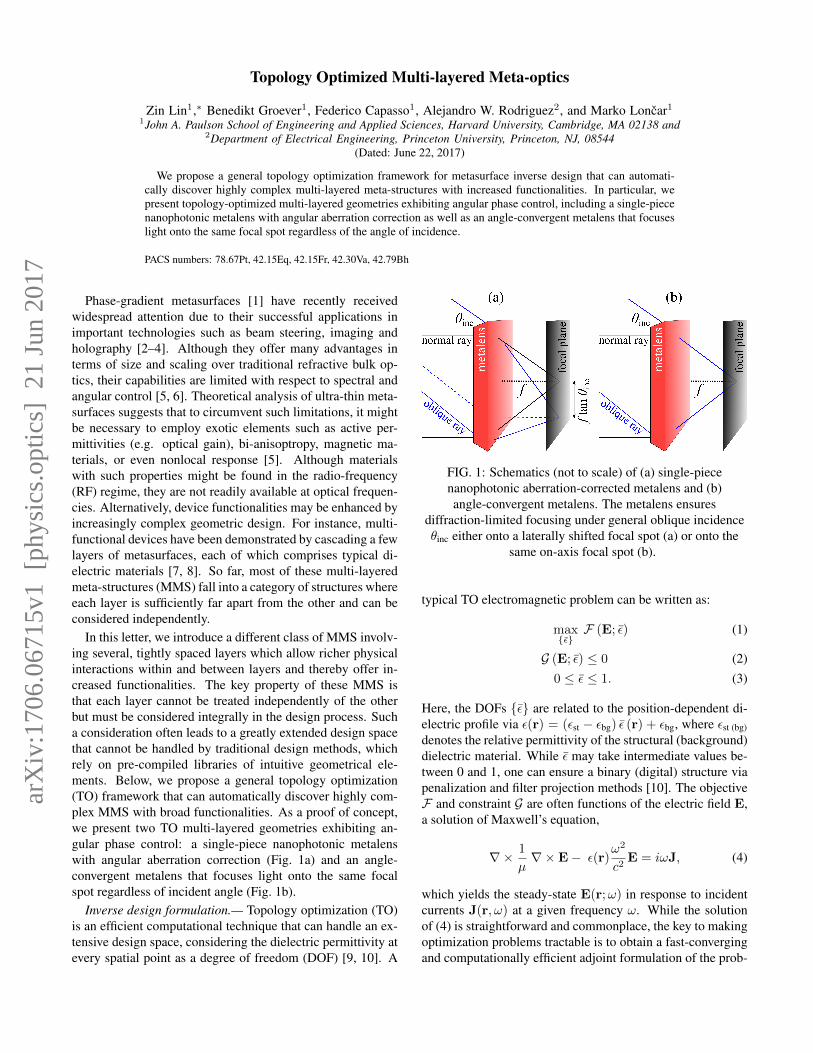
In this letter, we introduce a different class of MMS involv-ing several, tightly spaced layers which allow richer physicalinteractions within and between layers and thereby offer in-creased functionalities. The key property of these MMS isthat each layer cannot be treated independently of the otherbut must be considered integrally in the design process. Sucha consideration often leads to a greatly extended design spacethat cannot be handled by traditional design methods, whichrely on pre-compiled libraries of intuitive geometrical ele-ments. Below, we propose a general topology optimization(TO) framework that can automatically discover highly com-plex MMS with broad functionalities. As a proof of concept,we present two TO multi-layered geometries exhibiting an-gular phase control: a single-piece nanophotonic metalenswith angular aberration correction (Fig. 1a) and an angle-convergent metalens that focuses light onto the same focalspot regardless of incident angle (Fig. 1b).
Inverse design formulation.— Topology optimization (TO)is an efficient computational technique that can handle an ex-tensive design space, considering the dielectric permittivity atevery spatial point as a degree of freedom (DOF) [9, 10]. A
met
alen
s
f ta
n θ
inc
(a)
normal ray
θinc
oblique ray
f
FIG. 1: Schematics (not to scale) of (a) single-piecenanophotonic aberration-corrected metalens and (b)angle-convergent metalens. The metalens ensures
diffraction-limited focusing under general oblique incidenceθinc either onto a laterally shifted focal spot (a) or onto the
same on-axis focal spot (b).
typical TO electromagnetic problem can be written as:
max{ε}F (E; ε) (1)
G (E; ε) ≤ 0 (2)0 ≤ ε ≤ 1. (3)
Here, the DOFs {ε} are related to the position-dependent di-electric profile via ε(r) = (εst − εbg) ε (r) + εbg, where εst (bg)denotes the relative permittivity of the structural (background)dielectric material. While ε may take intermediate values be-tween 0 and 1, one can ensure a binary (digital) structure viapenalization and filter projection methods [10]. The objectiveF and constraint G are often functions of the electric field E,a solution of Maxwell’s equation,
∇× 1
µ∇×E− ε(r)
ω2
c2E = iωJ, (4)
which yields the steady-state E(r;ω) in response to incidentcurrents J(r, ω) at a given frequency ω. While the solutionof (4) is straightforward and commonplace, the key to makingoptimization problems tractable is to obtain a fast-convergingand computationally efficient adjoint formulation of the prob-
arX
iv:1
706.
0671
5v1
[ph
ysic
s.op
tics]
21
Jun
2017

2
0° 7.5°
15° 20°
0° 7.5°15° 20°
(a)
(b)
0 10-10
Inte
nsit
y (
a.u
)
1.0
0.6
0.2
r/
0°7.5°15°
20°
(c)
(d)
x
y
23
0° 7.5°
15° 20°
(e)
40
20
x
y
x
y
FIG. 2: (a) Multi-layered miniature 2D lens (NA = 0.35, f = 30λ) which is aberration-corrected for four incident angles{0◦, 7.5◦, 15◦, 20◦}. Note that by virtue of symmetry, the lens is automatically corrected for the negative angles as well{−7.5◦,−15◦,−20◦}. The lens materials consist of five layers of silicon (black) in alumina matrix (gray). A portion of thelens is magnified for easy visualization (inset); the smallest features (such as those encircled within blue dotted oval lines)measure 0.02λ while the thickness of each layer is 0.2λ. (b) FDTD analysis of the far field profiles (density plots) reveal
focusing action for the four incident angles. Note that the location of the focal plane is denoted by a white dashed line. (c) Thefield intensities (circle points) at the focal plane follow the ideal diffraction limit (solid lines). Note that the intensities are
normalized to unity for an easy comparison of the spot sizes. (d) The corresponding phase profile (red circle data points) foreach angle is measured at a distance of 1.5λ from the device, showing good agreement with the ideal profile (black solid line).
(e) Near-field profiles with almost perfect out-going spherical wavefronts.
lem. Within the scope of TO, this requires efficient calcula-tions of the derivatives ∂F
∂ε(r) ,∂G∂ε(r) at every spatial point r,
performed by exploiting the adjoint-variable method [10].
Recently, inverse-design techniques based on TO have beensuccessfully applied to a variety of photonic systems includ-ing on-chip mode splitters, nonlinear frequency convertersand Dirac cone photonic crystals [10–18]. However, to thebest of our knowledge, there is an apparent lack of large-scalecomputational techniques specifically tailored for metasurfacedesign, with the possible exception of Ref. [19], which is lim-ited to grating deflectors. Here, we introduce a general opti-mization framework for designing a generic meta-optics de-vice, single or multi-layered, with arbitrary phase response.The key to our formulation is the familiar superposition prin-ciple: given a desired phase profile φ(r), the ideal wavefronteiφ(r) and the complex electric field E(r) will constructively
interfere if and only if their phase difference vanishes. Defin-ing E(r) = E(r) · e for a given polarization e, we define thefollowing optimization function:
F(ε) =1
V
∫ ∣∣∣E(r) + eiφ(r)∣∣∣2 − ∣∣∣E(r)
∣∣∣2 − 1
2∣∣∣E(r)
∣∣∣ dr, (5)
where V =∫dr and the spatial integration is performed
over a reference plane (typically one or two wavelengths awayfrom the meta-device) where φ(r) is defined. Note that F isnone other than a spatially-averaged cosine of the phase dif-ference between eiφ(r) and E(r),
F(ε) =1
V
∫cos (argE(r)− φ(r)) dr,
3
0° 3°
6° 9°
0 10-10
Inte
nsit
y (
a.u
)
1.0
0.6
0.2
r/
0° 3°6° 9°
-5 5
3°****
0°
6°9°
(a)
(b) (c)
(d)
x
y
23
20
20
(e)0° 3°
6° 9°
x
y
x
y
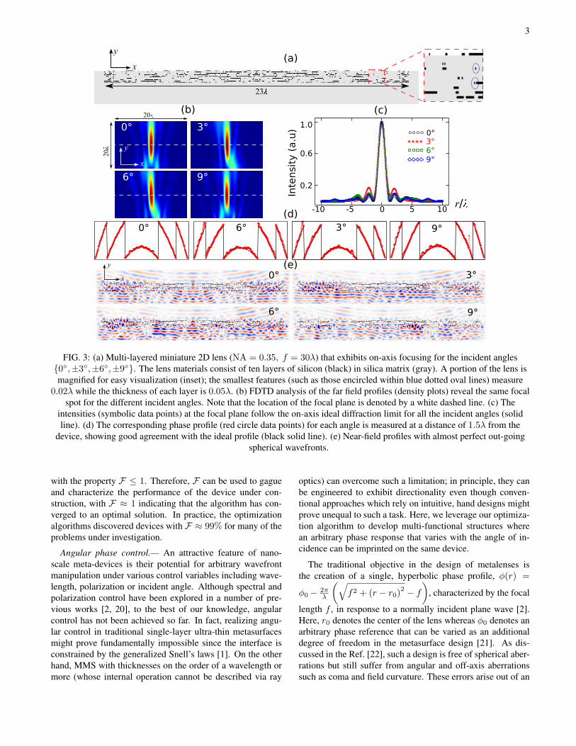
FIG. 3: (a) Multi-layered miniature 2D lens (NA = 0.35, f = 30λ) that exhibits on-axis focusing for the incident angles{0◦,±3◦,±6◦,±9◦}. The lens materials consist of ten layers of silicon (black) in silica matrix (gray). A portion of the lens ismagnified for easy visualization (inset); the smallest features (such as those encircled within blue dotted oval lines) measure
0.02λ while the thickness of each layer is 0.05λ. (b) FDTD analysis of the far field profiles (density plots) reveal the same focalspot for the different incident angles. Note that the location of the focal plane is denoted by a white dashed line. (c) The
intensities (symbolic data points) at the focal plane follow the on-axis ideal diffraction limit for all the incident angles (solidline). (d) The corresponding phase profile (red circle data points) for each angle is measured at a distance of 1.5λ from the
device, showing good agreement with the ideal profile (black solid line). (e) Near-field profiles with almost perfect out-goingspherical wavefronts.
with the property F ≤ 1. Therefore, F can be used to gagueand characterize the performance of the device under con-struction, with F ≈ 1 indicating that the algorithm has con-verged to an optimal solution. In practice, the optimizationalgorithms discovered devices with F ≈ 99% for many of theproblems under investigation.
Angular phase control.— An attractive feature of nano-scale meta-devices is their potential for arbitrary wavefrontmanipulation under various control variables including wave-length, polarization or incident angle. Although spectral andpolarization control have been explored in a number of pre-vious works [2, 20], to the best of our knowledge, angularcontrol has not been achieved so far. In fact, realizing angu-lar control in traditional single-layer ultra-thin metasurfacesmight prove fundamentally impossible since the interface isconstrained by the generalized Snell’s laws [1]. On the otherhand, MMS with thicknesses on the order of a wavelength ormore (whose internal operation cannot be described via ray
optics) can overcome such a limitation; in principle, they canbe engineered to exhibit directionality even though conven-tional approaches which rely on intuitive, hand designs mightprove unequal to such a task. Here, we leverage our optimiza-tion algorithm to develop multi-functional structures wherean arbitrary phase response that varies with the angle of in-cidence can be imprinted on the same device.
The traditional objective in the design of metalenses isthe creation of a single, hyperbolic phase profile, φ(r) =
φ0− 2πλ
(√f2 + (r − r0)
2 − f)
, characterized by the focal
length f , in response to a normally incident plane wave [2].Here, r0 denotes the center of the lens whereas φ0 denotes anarbitrary phase reference that can be varied as an additionaldegree of freedom in the metasurface design [21]. As dis-cussed in the Ref. [22], such a design is free of spherical aber-rations but still suffer from angular and off-axis aberrationssuch as coma and field curvature. These errors arise out of an
4
incorrect phase profile that skews the oblique off-axis rays. Acorrected phase profile free from aberration is therefore nec-essarily angle-dependent, as given by:
φ (r, θinc) = φ0(θinc)− 2πλ
(√f2 + (r − r0 − f tan θinc)
2 − f).
Note that the above expression can be deduced by consid-ering the optical path length contrast between a generic rayand the orthonormal ray directed towards a focusing spot lat-erally shifted by f tan θinc (see Fig. 1a, blue dashed line).Here, we leverage our TO algorithm to design a 2D minia-ture angle-corrected metalens that exactly embodies the idealangle-dependent phase profile given above. Note that thoughour miniature design is a proof-of-concept theoretical proto-type, it is completely straightforward (though computation-ally intensive) to design a full 3D wide-area (centimeter-scale)single-piece monochromatic aberration-free lens using ourTO technique. We emphasize that such a “next generation”lens fundamentally differs from the traditional aberration-corrected doublet because the latter exclusively relies on clas-sical ray tracing techniques whereas the former intricately ex-ploits nano-scale electromagnetic effects to achieve angularcontrol.
We design a lens with an NA of 0.35 and a focal length of30λ. The device consists of five layers of topology-optimizedaperiodic silicon gratings (invariant along z) against amor-phous alumina background (Fig. 2a). Each silicon layer is0.2λ thick and is separated by 0.1λ alumina gaps. We specif-ically chose silicon and alumina with a view to eventual fab-rication at mid or far IR wavelengths (5 − 8 µm) by stackingpatterned 2D slabs via repeated lithography, material depo-sition and planarization processes [23, 24]. The entire lenshas a thickness of 1.5λ, offering ample space for complexelectromagnetic interactions while, at the same time, main-taining orders of magnitude smaller thickness compared totraditional multi-lens systems. The lens is aberration cor-rected for four incident angles {0◦, 7.5◦, 15◦, 20◦} as wellas their negative counterparts {−7.5◦,−15◦,−20◦}. Notethat the largest possible angle for diffraction-limited focus-ing is ≈ 21◦ and is determined by the numerical aperture.For simplicity, we consider off-axis propagation in the xyplane with an s-polarized electric field parallel to the direc-tion of the gratings, E = E(r)z. FDTD analysis of the farfield (Fig. 2b) reveals focusing action with diffraction lim-ited intensity profiles (Fig. 2c), while the transmission effi-ciencies average around 25% for the four angles. To eval-uate the deviation of our design from the ideal phase pro-file, we computed the wave aberration function (WAF) foreach angle [22], obtaining WAF(0◦,±7.5◦,±15◦,±20◦) =(0.07, 0.04, 0.06, 0.08), which clearly satisfy the Marechalcriterion WAF ≤ 1
14 except for the 20◦ incident angle. Theerrors in the latter case primarily arise from the difficulty overoptimizing the extremities of the lens, which can be miti-gated by extending the optimized lens area (or equivalentlydesigning a larger NA). It is worth noting that the residualphase errors apparent in the optimized design primarily stem
from a need to force the optimal design to be binary whilebeing constrained by a limited resolution. In this work, weimplemented a spatial resolution step size ∆r = λ/50 overa 23λ-long simulation domain while our optimization algo-rithm handles approximately 5600 degrees of freedom. Theseparameters are solely dictated by the limited computationalresources currently available to us. We find that without thebinary constraint (i.e. when each DOF is allowed to take in-termediate values between 0 and 1), the optimal designs easilyachieve perfect phase profiles with WAFs smaller than 0.01.We expect that given better computational facilities, optimiza-tion over higher resolution domains will lead to fully binarystructures that also preserve vanishing WAF ≈ 0.
Next, to demonstrate the versatility of our approach, we de-sign a 2D metalens that focuses light onto the same spot re-gardless of the angle of incidence (Fig. 1b) – a device whichwe will choose to call angle-convergent metalens. Specif-ically, we impose the phase profile φ(r) = φ0 (θinc) −2πλ
(√f2 + (r − r0)
2 − f)
on the outgoing field under mul-
tiple discrete incident angles {0◦,±3◦,±6◦,±9◦}. The lenshas an NA of 0.35 and a focal length of 30λ. The lens ma-terials consist of ten layers of 0.05λ thick silicon in silicaseparated by 0.05λ gaps (Fig. 3a), making the entire deviceapproximately one λ thick. Such a device can be fabricatedusing advanced 3D photonic integration techniques [23], in-cluding those enabled by CMOS foundries [25]. Far fieldanalysis (Fig. 3b) shows focusing action at the same fo-cal spot for all the angles. Although the field intensitiesat the focal spot do not exactly follow the profile of anideal Airy disk due to residual phase errors, their band-width (aka full width at half maximum) clearly satisfies thediffraction limit (Fig. 3c). The diffraction-limited focusingis also consistent with small WAFs which are found to sat-isfy the Marechal criterion: WAF(0◦,±3◦,±6◦,±9◦) =(0.02, 0.04, 0.04, 0.02) < 1/14. The transmission efficiencyof the device averages around 15% over all angles.
Conclusion and outlook.— To summarize, we proposed ageneral optimization framework for inverse design of multi-layered meta-optics. We leveraged our formulation to engi-neer angular phase control in multi-layered metalens. It is im-portant to note that, in this paper, as we focus on establishingthe validity and versatility of our optimization approach, wehave not sought to pursue “the best possible design” for anyparticular problem that we chose to investigate. For example,the number, positioning and thicknesses of layers are arbitrar-ily chosen in each problem. It is entirely possible that de-pending on the desired level of performance, one can achieveviable designs using fewer and/or thicker layers, which couldrender the entire device even thinner and easier to fabricate.
While the optimization framework we have proposed ex-clusively focuses on phase, work is currently under way toimplement additional features such as amplitude uniformityand high efficiency constraints, which can be straightfor-wardly added to our formulation. Although the addition of ex-tra conditions would presumably strain the optimization pro-
5
cess, we expect that a full 3D multi-layered device platformshould be able to accommodate any additional demands. Ul-timately, we surmise that multi-layered volumetric structures(no more than a few wavelengths thick) will help deliver un-precedented wavefront manipulation capabilities at the nano-scale that involve phase, intensity and polarization controlas well as spectral and angular dispersion engineering alto-gether in a single device. The TO technique is by far themost efficient tool that can handle the enormous design spaceavailable to such platforms. Although fabrication of multi-layered nanostructures might prove challenging for shorteroperational wavelengths, they can be readily implemented inmid to far IR regimes, through state-of-the-art 3D fabricationtechnologies [23] such as two-photon lithography [26] andlaser writing processes [27], advanced foundry access [25] aswell as ultra-high resolution EUV lithography [28].
Acknowledgements.— We would like to thank Raphael Pes-tourie, Steven Johnson, Pawel Latawiec, Robert Devlin, Wei-Ting Chen and Alexander Zhu for useful discussions. Z. Lin issupported by the National Science Foundation Graduate Re-search Fellowship Program under Grant No. DGE1144152.The work was partially supported by the Air Force Officeof Scientific Research (MURI grant no. FA9550-14-1-0389),by the National Science Foundation under Grant No. DMR-1454836, by the National Science Foundation under EFRI-1005093 and by the Princeton Center for Complex Materials,a MRSEC supported by NSF Grant No. DMR 1420541.
∗ [email protected][1] Nanfang Yu, Patrice Genevet, Mikhail A Kats, Francesco Aieta,
Jean-Philippe Tetienne, Federico Capasso, and Zeno Gaburro.Light propagation with phase discontinuities: generalized lawsof reflection and refraction. science, 334:333, 2011.
[2] Francesco Aieta, Mikhail A Kats, Patrice Genevet, and Fed-erico Capasso. Multiwavelength achromatic metasurfaces bydispersive phase compensation. Science, 347:1342, 2015.
[3] Amir Arbabi, Yu Horie, Mahmood Bagheri, and Andrei Faraon.Dielectric metasurfaces for complete control of phase and po-larization with subwavelength spatial resolution and high trans-mission. Nature Nanotechnology, 10:937, 2015.
[4] Mohammadreza Khorasaninejad, Wei Ting Chen, Robert C De-vlin, Jaewon Oh, Alexander Y Zhu, and Federico Capasso.Metalenses at visible wavelengths: Diffraction-limited focus-ing and subwavelength resolution imaging. Science, 352:1190,2016.
[5] Nasim Mohammadi Estakhri and Andrea Alu. Wave-fronttransformation with gradient metasurfaces. Physical Review X,6:041008, 2016.
[6] Amir Arbabi and Andrei Faraon. Fundamental limits of ultra-thin metasurfaces. Scientific Reports, 7:43722, 2017.
[7] Amir Arbabi, Yu Horie, and Andrei Faraon. Planar retroreflec-tor. In Lasers and Electro-Optics (CLEO), page 1, 2014.
[8] Amir Arbabi, Ehsan Arbabi, Seyedeh Mahsa Kamali, Yu Horie,Seunghoon Han, and Andrei Faraon. Miniature optical planarcamera based on a wide-angle metasurface doublet correctedfor monochromatic aberrations. Nature Communications, 7,2016.
[9] Chiu Y Kao, Stanley Osher, and Eli Yablonovitch. Maximizingband gaps in two-dimensional photonic crystals by using levelset methods. Applied Physics B: Lasers and Optics, 81:235,2005.
[10] Jakob S Jensen and Ole Sigmund. Topology optimization fornano-photonics. Laser and Photonics Reviews, 5:308, 2011.
[11] Xiangdong Liang and Steven G Johnson. Formulation for scal-able optimization of microcavities via the frequency-averagedlocal density of states. Optics express, 21:30812, 2013.
[12] Jesse Lu and Jelena Vuckovic. Nanophotonic computationaldesign. Optics express, 21:13351, 2013.
[13] Han Men, Karen YK Lee, Robert M Freund, Jaime Peraire,and Steven G Johnson. Robust topology optimization of three-dimensional photonic-crystal band-gap structures. Optics ex-press, 22:22632, 2014.
[14] Alexander Y Piggott, Jesse Lu, Konstantinos G Lagoudakis, JanPetykiewicz, Thomas M Babinec, and Jelena Vuckovic. Inversedesign and demonstration of a compact and broadband on-chipwavelength demultiplexer. Nature Photonics, 9:374, 2015.
[15] Bing Shen, Peng Wang, Randy Polson, and Rajesh Menon. Anintegrated-nanophotonics polarization beamsplitter with 2.4×2.4 µm2 footprint. Nature Photonics, 9:378, 2015.
[16] Zin Lin, Xiangdong Liang, Marko Loncar, Steven G John-son, and Alejandro W Rodriguez. Cavity-enhanced second-harmonic generation via nonlinear-overlap optimization. Op-tica, 3:233, 2016.
[17] Zin Lin, Adi Pick, Marko Loncar, and Alejandro W Rodriguez.Enhanced spontaneous emission at third-order dirac excep-tional points in inverse-designed photonic crystals. PhysicalReview Letters, 117:107402, 2016.
[18] Zin Lin, Lysander Christakis, Yang Li, Eric Mazur, Alejan-dro W Rodriguez, and Marko Loncar. Topology-optimizedDual-Polarization Dirac Cones. ArXiv e-prints, 2017.
[19] David Sell, Jianji Yang, Sage Doshay, Rui Yang, andJonathan A Fan. Large angle, multi-functional metagratingsbased on freeform multi-mode geometries. Nano Letters, 2017.
[20] Jan P. Balthasar Mueller, Noah A Rubin, Robert C Devlin,Benedikt Groever, and Federico Capasso. Metasurface polar-ization optics: Independent phase control of arbitrary orthogo-nal states of polarization. Physical Review Letters, 118:113901,2017.
[21] Mohammadreza Khorasaninejad, Zhujun Shi, Alexander YZhu, Wei-Ting Chen, Vyshakh Sanjeev, Aun Zaidi, and Fed-erico Capasso. Achromatic metalens over 60 nm bandwidthin the visible and metalens with reverse chromatic dispersion.Nano Letters, 17:1819, 2017.
[22] Francesco Aieta, Patrice Genevet, Mikhail Kats, and FedericoCapasso. Aberrations of flat lenses and aplanatic metasurfaces.Optics express, 21:31530, 2013.
[23] Nicolas Sherwood-Droz and Michal Lipson. Scalable 3ddense integration of photonics on bulk silicon. Optics express,19:17758, 2011.
[24] Minghao Qi, Elefterios Lidorikis, Peter T Rakich, Steven GJohnson, JD Joannopoulos, Erich P Ippen, and Henry I Smith.A three-dimensional optical photonic crystal with designedpoint defects. Nature, 429:538, 2004.
[25] Michael Hochberg and Tom Baehr-Jones. Towards fabless sili-con photonics. Nature Photonics, 4:492, 2010.
[26] Timo Gissibl, Simon Thiele, Alois Herkommer, and HaraldGiessen. Two-photon direct laser writing of ultracompact multi-lens objectives. Nature Photonics, 10:554, 2016.
[27] Fabian Niesler and Yann Tanguy. 3d printers for the fabricationof micro-optical elements. Optik & Photonik, 11:44, 2016.
[28] Charles W Gwyn, R Stulen, D Sweeney, and D Attwood. Ex-
6
treme ultraviolet lithography. Journal of Vacuum Science &Technology B: Microelectronics and Nanometer Structures Pro-cessing, Measurement, and Phenomena, 16:3142, 1998.
SUPPLEMENT
PHASE PROFILE OF AN IDEAL ABERRATION-FREELENS
Here, we examine the angle-dependent phase profile neces-sary to correct monochromatic aberrations in a lens:
φ (r, θinc) = c(θinc)−2π
λ
(√f2 + (f tan θinc − r + r0)
2 − f).
(S1)
Here, r0 is the origin of the lens. It is easily seen that theaberration-corrected φ (r, θinc) is simply a hyperbolic profileshifted by a distance f tan θinc which is the location of focalspot in the far field. When the angle of incidence θinc is zero,we obtain the familiar hyperbolic phase profile for the normalincidence. Given φ(r), we can exactly compute the far fieldby convoluting with the standard Green’s function propagator:
Efar (r, θinc) ∝∫eik|r−r
′|
|r− r′|eiφ(r′,θinc)dr′ (S2)
In our paper, we have exactly computed the ideal far fieldintensity profile based on the convolution integral above(Eq. S2) and compared it with the simulated far field of theoptimized design for each incident angle. It should be notedthat for sin θinc & NA, the width (FWHM) of the far fieldbegins to violate the diffraction limit > λ
2NA .
COMPARISON AGAINST STANDARDNORMAL-INCIDENCE METALENS DESIGN
We examine the standard single-layered metalens (NA =0.35, f = 30λ) with the same parameters as our topology-optimized aberration-corrected design given in the main text.
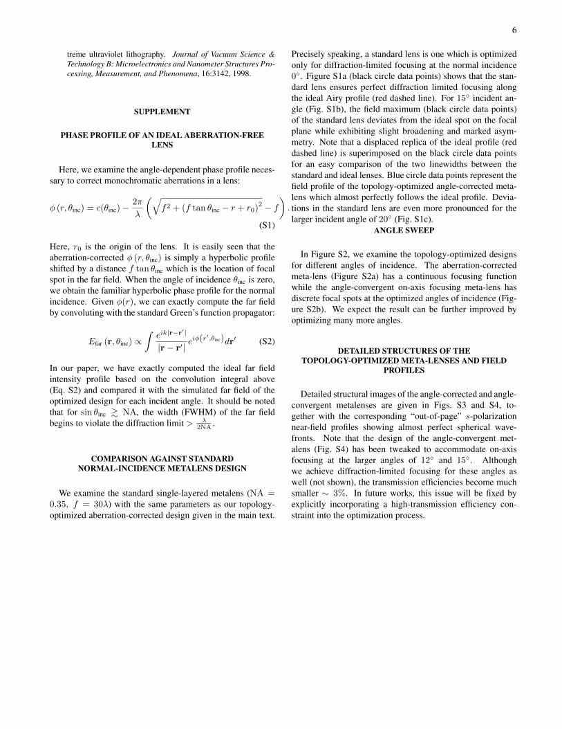
Precisely speaking, a standard lens is one which is optimizedonly for diffraction-limited focusing at the normal incidence0◦. Figure S1a (black circle data points) shows that the stan-dard lens ensures perfect diffraction limited focusing alongthe ideal Airy profile (red dashed line). For 15◦ incident an-gle (Fig. S1b), the field maximum (black circle data points)of the standard lens deviates from the ideal spot on the focalplane while exhibiting slight broadening and marked asym-metry. Note that a displaced replica of the ideal profile (reddashed line) is superimposed on the black circle data pointsfor an easy comparison of the two linewidths between thestandard and ideal lenses. Blue circle data points represent thefield profile of the topology-optimized angle-corrected meta-lens which almost perfectly follows the ideal profile. Devia-tions in the standard lens are even more pronounced for thelarger incident angle of 20◦ (Fig. S1c).
ANGLE SWEEP
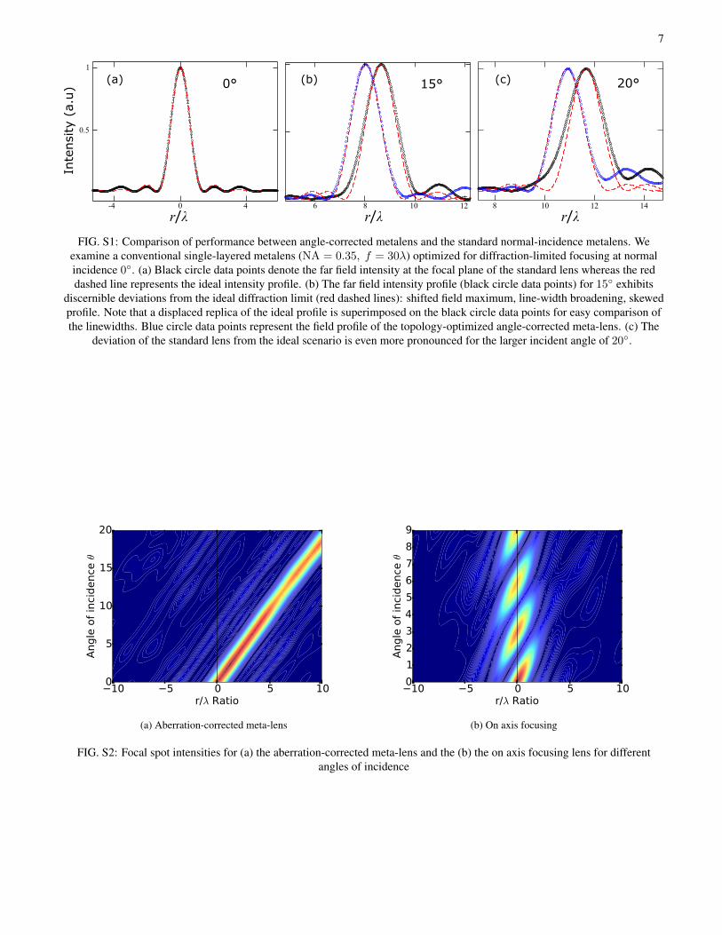
In Figure S2, we examine the topology-optimized designsfor different angles of incidence. The aberration-correctedmeta-lens (Figure S2a) has a continuous focusing functionwhile the angle-convergent on-axis focusing meta-lens hasdiscrete focal spots at the optimized angles of incidence (Fig-ure S2b). We expect the result can be further improved byoptimizing many more angles.
DETAILED STRUCTURES OF THETOPOLOGY-OPTIMIZED META-LENSES AND FIELD
PROFILES
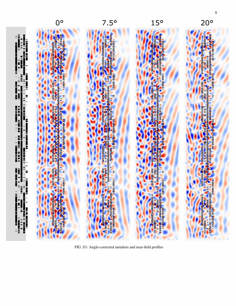
Detailed structural images of the angle-corrected and angle-convergent metalenses are given in Figs. S3 and S4, to-gether with the corresponding “out-of-page” s-polarizationnear-field profiles showing almost perfect spherical wave-fronts. Note that the design of the angle-convergent met-alens (Fig. S4) has been tweaked to accommodate on-axisfocusing at the larger angles of 12◦ and 15◦. Althoughwe achieve diffraction-limited focusing for these angles aswell (not shown), the transmission efficiencies become muchsmaller ∼ 3%. In future works, this issue will be fixed byexplicitly incorporating a high-transmission efficiency con-straint into the optimization process.
7
-4 0 4
0.5
1
6 8 10 12 8 10 12 14
Inte
nsity (
a.u
)
r/λ
0° 15° 20°
r/λr/λ
(a) (b) (c)
FIG. S1: Comparison of performance between angle-corrected metalens and the standard normal-incidence metalens. Weexamine a conventional single-layered metalens (NA = 0.35, f = 30λ) optimized for diffraction-limited focusing at normalincidence 0◦. (a) Black circle data points denote the far field intensity at the focal plane of the standard lens whereas the reddashed line represents the ideal intensity profile. (b) The far field intensity profile (black circle data points) for 15◦ exhibits
discernible deviations from the ideal diffraction limit (red dashed lines): shifted field maximum, line-width broadening, skewedprofile. Note that a displaced replica of the ideal profile is superimposed on the black circle data points for easy comparison ofthe linewidths. Blue circle data points represent the field profile of the topology-optimized angle-corrected meta-lens. (c) The
deviation of the standard lens from the ideal scenario is even more pronounced for the larger incident angle of 20◦.
−10 −5 0 5 10r/λ Ratio
0
5
10
15
20
Angle
of
inci
dence
θ
(a) Aberration-corrected meta-lens
−10 −5 0 5 10r/λ Ratio
0
1
2
3
4
5
6
7
8
9
Angle
of
inci
dence
θ
(b) On axis focusing
FIG. S2: Focal spot intensities for (a) the aberration-corrected meta-lens and the (b) the on axis focusing lens for differentangles of incidence
8
0° 7.5° 15° 20°
FIG. S3: Angle-corrected metalens and near-field profiles

9
0° 3° 6° 9° 12° 15°
FIG. S4: Angle-convergent metalens and near-field profiles
Related Documents


![Investigation of optimized topology for AC/DC Power supply ......No Topology Feature Power(W) PeakEfficiency(%) Ref. 1 Buck Highgain 500 98.5 [10] Cascaded 2000 97 [11] 2 SEPIC UsesSiC](https://static.cupdf.com/doc/110x72/60a418280d88577b255847b3/investigation-of-optimized-topology-for-acdc-power-supply-no-topology-feature.jpg)


