Topological Surface Transport Properties of Single-Crystalline SnTe Nanowire Muhammad Safdar, † Qisheng Wang, † Misbah Mirza, Zhenxing Wang, Kai Xu, and Jun He* National Center for Nanoscience and Technology, Beijing 100190, China * S Supporting Information ABSTRACT: SnTe has attracted worldwide interest since its theoretical predication as topological crystalline insulator. Because of promising applications of one-dimensional topo- logical insulator in nanoscale electronics and spintronics device, it is very important to realize the observation of topological surface states in one-dimensional SnTe. In this work, for the first time we successfully synthesized high-quality single crystalline SnTe nanowire via gold-catalyst chemical vapor deposition method. Systematical investigation of Aharonov- Bohm and Shubnikov-de Haas oscillations in single SnTe nanowire prove the existence of Dirac electrons. Further analysis of temperature-dependent Shubnikov-de Haas oscillations gives valuable information of cyclotron mass, mean-free path, and mobility of Dirac electrons in SnTe nanowire. Our study provides the experimental groundwork for research in low- dimensional topological crystalline insulator materials and paves the way for the application of SnTe nanowire in nanoelectronics and spintronics device. KEYWORDS: Single-crystalline SnTe nanowires, topological crystalline insulators, Aharonov-Bohm interference, Shubnikov-de Haas oscillations T opological insulators (TIs), an unusual quantum state of matter, are characterized by a gapless metallic surface state and insulating bulk gap. 1 On the surface of TIs, the electron spin is locked perpendicular to the momentum, which make the surface state of TIs immune to any time reversal perturbations such as nonmagnetic impurities and crystal defects. 2-4 These unique properties make TIs promising applications in novel spintronics and low-dissipation quantum computation. 5,6 In addition, TIs provides the basis of materials for realization of unique quantum mechanical effect such as quantum anomalous hall effect 7 and Majorana fermions. 5 The discovery of three-dimensional (3D) TIs protected by time-reversal symmetry 8 such as Bi 2 Te 3 , Sb 2 Te 3 , and Bi 2 Se 3 has simulated the search of new topological insulator protected by other symmetries. For example, topological crystalline insu- lators (TCIs), 9 a new topological state, are found to be protected by crystal symmetry. Among various materials, tin telluride (SnTe) with a rocksalt structure shows special mirror symmetry in face-centered cubic Brillouin zone. It has been predicted as the first distinctive type of TCIs where conductive surface states are expected on the highly symmetrical crystal surface of SnTe such as {001}, {110} and {111}. 10 Since the discovery of SnTe as remarkable TCIs, it has attracted worldwide interest and opens the gateway to the theoretical and experimental research of TCIs. Significantly, SnTe is a simple stoichiometric compound compared with other TCIs such as Pb 1-x Sn x Te, 11 which make it easier to be synthesized. Recently, Tanaka 12 et al. experimentally confirmed the existence of a metallic Dirac-cone surface state on the (001) surface of SnTe bulk crystals by angle-resolved photoemission spectra. However, very few magneto-transport measurements of TCIs SnTe, 13 a straightforward way to probe the surface topological states, have been reported presumably due to the dominant transport of bulk carriers from crystal defects and thermal excitations. 3 Compared with bulk counterparts, nanostructure TIs materials are highly competitive system for investigating the surface topological nature due to their large surface-to-volume ratio, 14-16 leading to an enhancement of contribution of topological surface carriers. In addition, nanostructures of TIs play a vital role for fundamental investigation of materials such as exotic surface states and spintronics applications. 17-19 As a result, it is of particular important to study the surface electronic state of TCI SnTe nanostructures by magneto- transport experiment. However, to the best of our knowledge, there is no experiment evidence showing the topological crystalline insulator nature of SnTe nanostructure. This may be due to the challenges in synthesis of high quality single crystalline low-dimensional SnTe nanosturctures. Here, we report for the first time the synthesis of highly single crystalline SnTe nanowire via gold-catalyst chemical vapor deposition (CVD) and the observation of topological Received: July 30, 2013 Revised: October 22, 2013 Letter pubs.acs.org/NanoLett © XXXX American Chemical Society A dx.doi.org/10.1021/nl402841x | Nano Lett. XXXX, XXX, XXX-XXX

Welcome message from author
This document is posted to help you gain knowledge. Please leave a comment to let me know what you think about it! Share it to your friends and learn new things together.
Transcript
Topological Surface Transport Properties of Single-Crystalline SnTeNanowireMuhammad Safdar,† Qisheng Wang,† Misbah Mirza, Zhenxing Wang, Kai Xu, and Jun He*
National Center for Nanoscience and Technology, Beijing 100190, China
*S Supporting Information
ABSTRACT: SnTe has attracted worldwide interest since itstheoretical predication as topological crystalline insulator.Because of promising applications of one-dimensional topo-logical insulator in nanoscale electronics and spintronics device,it is very important to realize the observation of topologicalsurface states in one-dimensional SnTe. In this work, for thefirst time we successfully synthesized high-quality singlecrystalline SnTe nanowire via gold-catalyst chemical vapordeposition method. Systematical investigation of Aharonov-Bohm and Shubnikov-de Haas oscillations in single SnTenanowire prove the existence of Dirac electrons. Furtheranalysis of temperature-dependent Shubnikov-de Haas oscillations gives valuable information of cyclotron mass, mean-freepath, and mobility of Dirac electrons in SnTe nanowire. Our study provides the experimental groundwork for research in low-dimensional topological crystalline insulator materials and paves the way for the application of SnTe nanowire in nanoelectronicsand spintronics device.
KEYWORDS: Single-crystalline SnTe nanowires, topological crystalline insulators, Aharonov-Bohm interference,Shubnikov-de Haas oscillations
Topological insulators (TIs), an unusual quantum state ofmatter, are characterized by a gapless metallic surface state
and insulating bulk gap.1 On the surface of TIs, the electronspin is locked perpendicular to the momentum, which make thesurface state of TIs immune to any time reversal perturbationssuch as nonmagnetic impurities and crystal defects.2−4 Theseunique properties make TIs promising applications in novelspintronics and low-dissipation quantum computation.5,6 Inaddition, TIs provides the basis of materials for realization ofunique quantum mechanical effect such as quantum anomaloushall effect7 and Majorana fermions.5
The discovery of three-dimensional (3D) TIs protected bytime-reversal symmetry8 such as Bi2Te3, Sb2Te3, and Bi2Se3 hassimulated the search of new topological insulator protected byother symmetries. For example, topological crystalline insu-lators (TCIs),9 a new topological state, are found to beprotected by crystal symmetry. Among various materials, tintelluride (SnTe) with a rocksalt structure shows special mirrorsymmetry in face-centered cubic Brillouin zone. It has beenpredicted as the first distinctive type of TCIs where conductivesurface states are expected on the highly symmetrical crystalsurface of SnTe such as {001}, {110} and {111}.10 Since thediscovery of SnTe as remarkable TCIs, it has attractedworldwide interest and opens the gateway to the theoreticaland experimental research of TCIs. Significantly, SnTe is asimple stoichiometric compound compared with other TCIssuch as Pb1−xSnxTe,
11 which make it easier to be synthesized.Recently, Tanaka12 et al. experimentally confirmed the
existence of a metallic Dirac-cone surface state on the (001)surface of SnTe bulk crystals by angle-resolved photoemissionspectra. However, very few magneto-transport measurements ofTCIs SnTe,13 a straightforward way to probe the surfacetopological states, have been reported presumably due to thedominant transport of bulk carriers from crystal defects andthermal excitations.3
Compared with bulk counterparts, nanostructure TIsmaterials are highly competitive system for investigating thesurface topological nature due to their large surface-to-volumeratio,14−16 leading to an enhancement of contribution oftopological surface carriers. In addition, nanostructures of TIsplay a vital role for fundamental investigation of materials suchas exotic surface states and spintronics applications.17−19 As aresult, it is of particular important to study the surfaceelectronic state of TCI SnTe nanostructures by magneto-transport experiment. However, to the best of our knowledge,there is no experiment evidence showing the topologicalcrystalline insulator nature of SnTe nanostructure. This may bedue to the challenges in synthesis of high quality singlecrystalline low-dimensional SnTe nanosturctures.Here, we report for the first time the synthesis of highly
single crystalline SnTe nanowire via gold-catalyst chemicalvapor deposition (CVD) and the observation of topological
Received: July 30, 2013Revised: October 22, 2013
Letter
pubs.acs.org/NanoLett
© XXXX American Chemical Society A dx.doi.org/10.1021/nl402841x | Nano Lett. XXXX, XXX, XXX−XXX
SAMI
Highlight
surface states in SnTe nanowire by quantum oscillationmeasurement. The quantum transport measurement of SnTenanowire shows well distinguished Aharonov-Bohm (AB)interference and Shubnikov-de Haas (SdH) oscillations. Deepanalysis of AB oscillation shows the existence of both h/e andh/2e quantum oscillations, giving the evidence of topologicalsurface states. Investigation of SdH oscillations indicates theexistence of π Berry phase, which demonstrates that quantumoscillation arises from two-dimensional Dirac fermions.Valuable parameters of topological surface states such ascyclotron mass, mean-free path, and mobility of Dirac electronsin SnTe nanowire are also estimated by analyzing thetemperature-dependent SdH oscillation.SnTe nanowires used in this work were synthesized in a
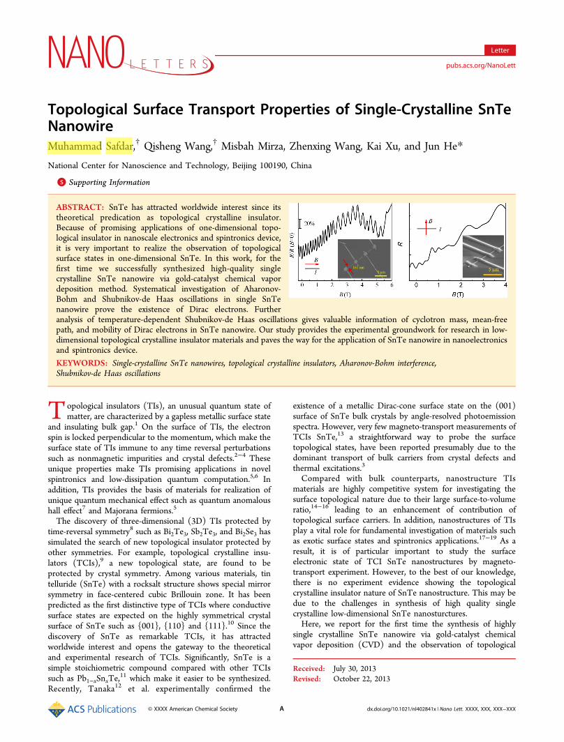
horizontal tube furnace via CVD method. Well-aligned anddense nanowires were obtained on Au-coated Si substrate withSnTe powder used as an evaporation source.20 More details ofthe growth process and characterization are described in theSupporting Information. SnTe has a cubic crystal structure withspace group Fm3m as described in Figure 1a. Schematicdiagram of electronic structure of SnTe (001) surface is alsoprovided in Supporting Information Figure S1.21 The typicallow-magnification scanning electron microscopy (SEM) imageshown in Figure 1b clearly illustrates the synthesized samplesare composed of dense nanowires with about 10 μm long. Thenanowires density of this substrate with deposition temperatureof 500 °C is estimated to be 1.7 × 10⁹/cm2 (SupportingInformation Figure S2a). High-magnification SEM image(Figure 1b inset) reveals the synthesized nanowires are about59 nm in diameter. The diameters of nanowires in this substrateprimarily distribute in 50−99 nm (75%), the diameters of othernanowires are in the range of 100−199 nm (25%), the average
diameter in this substrate is 98 nm (Supporting InformationFigure S2b). Transmission electron microscopy (TEM) imageof nanowire in Figure 1c exposes the presence of goldnanoparticle at the top of nanowire, suggesting the vapor−liquid−solid (VLS) growth mechanism. Magnified-TEM inSupporting Information Figure S3 shows top gold nanoparticleconnected perfectly with SnTe nanowire. High-quality AFMimages of several typical SnTe nanowires display cross-sectionshape of nanowire is mainly triangle (Figure 1d and SupportingInformation Figure S4). Detailed structural characterizationsusing high-resolution TEM (HRTEM) image in Figure 1edemonstrate that SnTe nanowires are in well-defined singlecrystal cubic phase with the lattice fringes of 0.315 nm,corresponding to (200) plane. Figure 1e also signifies thesurface of nanowire is smooth and has not been oxidized. It isfound that nanowire growth is along [020] direction. Thecorresponding selected area electron diffraction (SAED)pattern (inset of Figure 1e) indicates excellent single crystallineof SnTe. The crystal planes (002), (020), and (022) suggestthat the synthesized SnTe belongs to cubic crystal system(JCPDS 08-0487). Energy dispersive X-ray spectroscopy(EDS) study in Figure 1f indicates that nanowires have perfectstoichiometric ratio of Sn to Te 1:1, the peaks of copper, iron,and cobalt comes from copper grid. Moreover, no extra peaksare present in the X-ray diffraction pattern (Figure 1g) ofnanowires, which further confirms the crystalline nature andpure cubic phase of SnTe.AB oscillation originates from quantum interference of two
partial electron waves after completing closed trajectories whichencircle certain magnetic flux. In our study, we fabricatedstandard four terminal device for the observation of ABoscillation. Details of device fabrication and transport measure-
Figure 1. Microscopy measurement of SnTe nanowires. (a) Schematic view depictions of the cubic crystal structure of SnTe. (b) SEM images ofSnTe nanowires, inset is a high-magnification image. The scale bar in (b) is 10 μm and inset is 200 nm. (c) TEM images of single SnTe nanowirewith gold particle at the top. The scale bar in (c) is 200 nm. (d) AFM image of single SnTe nanowire, inset shows cross-section shape of SnTenanowire. (e) HRTEM images and SAED pattern (inset) of single crystalline SnTe nanowire, three white spots (000), (220), and (020), shaded bythe tip, were artificially added. The scale bar in (d) is 5 nm. (f) EDS of obtained SnTe nanowires. (g) XRD pattern of as prepared SnTe nanowires.
Nano Letters Letter
dx.doi.org/10.1021/nl402841x | Nano Lett. XXXX, XXX, XXX−XXXB
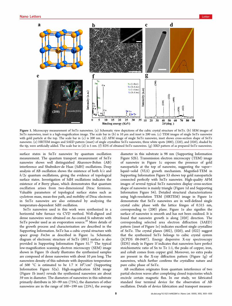
ments are given in Supporting Information. From Figure 2a, wecan see that the nanowire has near triangle shape with a bottomwidth w of 161 nm and height h (Figure 2a inset) of 240 nm,giving the cross-section area S = 1/2wh = 19 320 nm2. Whenapplied a parallel magnetic field along the length of thenanowire at temperature 20 K, the pronounced reproducibleoscillation is observed as shown in Figure 2b. A downwardsharp cusp at zero magnetic field shows the weakantilocalization effect, resulting from strong spin−orbitcoupling of Dirac electrons as occurred in other TIs.14,15,22 Afast Fourier transform (FFT) of magnetoresistance (MR)derivative dR/dB in Figure 2c displays prominent oscillationfrequency of h/e. In addition, an oscillation frequency of h/2e,known as the Altshuler−Aronov−Spival (AAS) effect, has alsobeen observed. The AAS effect, arising from quantuminterference of two interfering electron wave encircling themagnetic flux once, has been realized in carbon nanotubes,23
metal rings24 and TIs.15,25 Figure 2b shows AAS effect with theperiod of 0.165 T (Figure 2c inset) dominates at low magneticfield 0 < B < 2 T, proving the existence of weak(anti)localization with strong enough disorder.26 Conductanceoscillation is expected to have a period of h/2e in strongenough disorder topological insulator due to weak antilocaliza-tion away from the Dirac point.26 SnTe is an intrinsic heavy p-type doped semiconductor due to large amount of Sn vacanciesat finite temperature.27,28 Thus SnTe nanowire achieved fromour work is strongly enough disordered because a large quantityof holes likely exists inside SnTe nanowire. So AAS effect isintensely anticipated to occur in SnTe single crystallinenanowire at least in low magnetic field. However, with theincrease of field 2 T < B < 5.3 T, AB effect becomes dominant
with reproducible oscillation period of 0.313 T (Figure 2cinset). However, the perfect periodicity deteriorates whenmagnetic field reaches up to 5.3 T, which may due to aperiodicoscillation from bulk carriers at high magnetic field. Theobvious magnetoresistance oscillation has also observed at 2and 10 K as shown in Supporting Information Figure S5. Theperiod of AAS interference at 2 K is 0.169 T which is very closeto the results measured at 20 K.It is noted that, for the h/e AB effect period ΔB of AB
oscillation is related to the magnetic flux quantum Φ0 = h/e byΔB = Φ0/S, where S is the cross-sectional area of nanowire, h isthe planck’s constant, and e is the electron charge. Thus cross-sectional area of 13340 nm2 can be deduced from ABoscillation which is slightly smaller than the estimated cross-sectional area of 19 320 nm2 by SEM and atomic forcemicroscopy (AFM). It is known that metallic surface states ofSnTe exist on those surfaces with high symmetry such as {001},{110}, and {111}. Thus it is not like topological insulatorBi2Se3 nanoribbon15 or Ag2Te nanowire22 that spin-lockedDirac electron wave travels along the perimeter of nanoribbonor nanowire which forms a loop encircling magnetic flux. Loopsformed by two interfering partial wave are confined to high-symmetry crystal surface inside SnTe nanowire, leading to thedifferences between cross-section area of 13 340 nm2 obtainedfrom the oscillation and that of 19 320 nm2 estimated fromresults of SEM and AFM. This can be further verified throughangle-dependent AB oscillation. As shown in Figure 2d, with anincrease of angle θ between the nanowire and magnetic field,the oscillation period does not increase following ΔB(θ) =ΔB(0)/cos(θ). Here, ΔR represents the MR after subtractionof smooth background. If we suppose the normal direction of
Figure 2. AB oscillation of topological surface states in SnTe nanowire. (a) SEM image of four terminal device of SnTe nanowire with bottom widthof 161 nm and height of 240 nm. Inset: AFM indicates the triangular cross section of SnTe nanowire. (b) Normalized MR with applied parallelmagnetic field at 20 K. (c) FFT of the derivate dR/dB indicates two oscillation frequency h/e and h/2e. Inset: magnetic field positions of oscillationminima versus oscillation index gives oscillation period of 0.165 and 0.313 T. (d) Angle-dependent MR oscillation, the colored arrows indicate thefour oscillation periods. (e) Temperature dependence of MR oscillation, the period of MR oscillation keeps rather constant 0.15 T at 20, 25, and 30K. The angle between magnetic field and nanowire keeps 60°. To clearly display the periodicity of MR at 30 K, the MR is amplified by 5 times. (f)Temperature-dependent FFT amplitude of derivate dR/dB for both h/e and h/2e oscillation. Inset: aperiodic MR oscillation at 35 and 40 K indicatessurface states are suppressed by bulk carriers at high temperature.
Nano Letters Letter
dx.doi.org/10.1021/nl402841x | Nano Lett. XXXX, XXX, XXX−XXXC
loops is parallel to the growth direction of SnTe nanowire,loops may form on high-symmetry crystal surface (002), (200),(002 ) and (200) faces since the growth direction of SnTenanowire is [020]. However, loops are also possibly present onthe other high-symmetry crystal surface. The normal directionsof these loops are no longer parallel to growth direction ofSnTe nanowire. Consequently, even if angle increases to 60°,the oscillations still keep strong because normal direction ofsome loops may go along the direction of magnetic field.Next, we discuss the information of AB oscillation by
analyzing temperature-dependent MR oscillation as shown inFigure 2e. Although the temperature increases to 30 K, the ΔRstill shows markedly periodicity at the whole applied magneticfield region. As pointed out previously, the AAS effect ispredominant at low field. In addition, AAS effect is more robustthan AB effect against temperature because AAS effect is causedby quantum interference of two time-reversal turns of surfacestate moving. Thus periodic oscillation keeps powerful even atrelative high temperature. This can be further proved viacomparing temperature-dependent FFT amplitude of derivatedR/dB at each temperature as displayed in Figure 2f. FFTamplitude of oscillation h/e decreases sharply with increase oftemperature while FFT amplitude of oscillation h/2e almostkeeps the same. However, as the temperature reaches up to 35K, as shown in the inset of Figure 2f, the perfect periodicity ofMR oscillation gradually deteriorates with increase of magneticfield. Even more, no period has been observed at 40 K (Figure2f inset), which is likely due to that dominant transport of bulkcarriers smears oscillations of topological surface states at hightemperature. All of these behaviors suggest the existence of
Dirac electrons in SnTe nanowire. This can be directly provedby the following results of SdH oscillations.As a powerful tool, SdH oscillations are widely used to prove
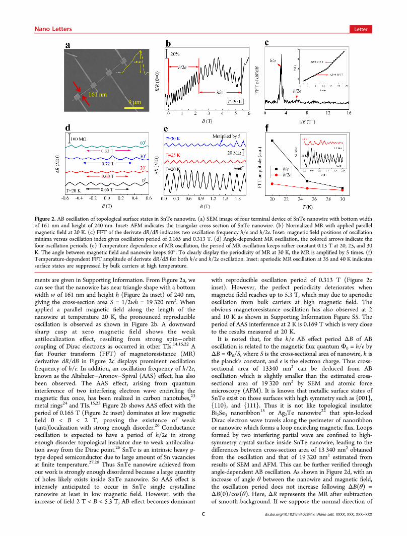
the existence of surface topological states.29 The relatively largewidth of 190 nm (Figure 3a) of SnTe nanowire make SdHoscillations measurement available due to that approximaterectangle shape provides large top and bottom surface asdisplayed in the AFM (Supporting Information Figure S6).Magneto-transport measurements were carried out at lowtemperature with magnetic field B aligned perpendicular to theSnTe nanowire. Figure 3b presents the plots of ΔR versus 1/Bat temperature of 2, 20, and 30 K, respectively. Strongoscillations can be observed at each temperature. Theoscillation amplitude increases with the increase of magneticfield, demonstrating the SdH oscillations. Red lines in Figure 3bshow the periodic oscillation of MR versus 1/B at eachtemperature. Figure 3c signifies a large positive MR effect ofSnTe nanowire with no saturation as B increases to 4 T. Anobvious downward cusp in MR at low field reflects theexistence of weak antilocalization effect expected in the TIs dueto the strong spin−orbit interaction and the helicity of thesurface states.14,15,30,31 Plot of MR versus 1/B (SupportingInformation Figure S7) exhibits perfect periodic oscillation asthe red line indicates, further verifying the SdH oscillation. TheFigure 3c inset shows the dependence of valley position onrotation angle θ, θ is the tilt angle between B and normaldirection of sample surface. The plot of valley position of n =4.5 versus tilt angle matches perfectly with fitting curve of 1/cos(θ) which are strongly expected in two-dimensional (2D)SdH oscillation.
Figure 3. SdH oscillation of surface states in SnTe nanowire. (a) A 45°-titled-view SEM image of four terminal device of SnTe nanowire with widthof 190 nm. (b) MR after subtraction of smooth background versus 1/B at 2, 20, and 30 K, red solid line shows the oscillation period remainsconstant with the increase of temperature. (c) MR versus B at 2 K with the magnetic field applied up to 4 T. Inset: valley position of n = 4.5 againsttilted angle θ, the data are consistent with the fitting plot of 1/cos(θ). (d) LL fan diagram constructed from MR oscillation. Inset: integer and semi-integer show the Landau level of peak and valley, respectively. (e) Temperature dependence of SdH oscillation amplitude at B = 0.72 T, givingcyclotron mass 0.015 me. Inset: comparison of resistance oscillation at 2 K with well-known SdH oscillation of ideal 2D Dirac electrons (γ = 1/2) andregular electrons (γ = 0). (f) Dingle plot of SdH oscillation at 2 K, indicating the Dingle temperature TD is 29 K, mean-free path lSdH is 33 nm andmobility of surface electron μs
SdH is 4866 cm2 V−1 s−1.
Nano Letters Letter
dx.doi.org/10.1021/nl402841x | Nano Lett. XXXX, XXX, XXX−XXXD
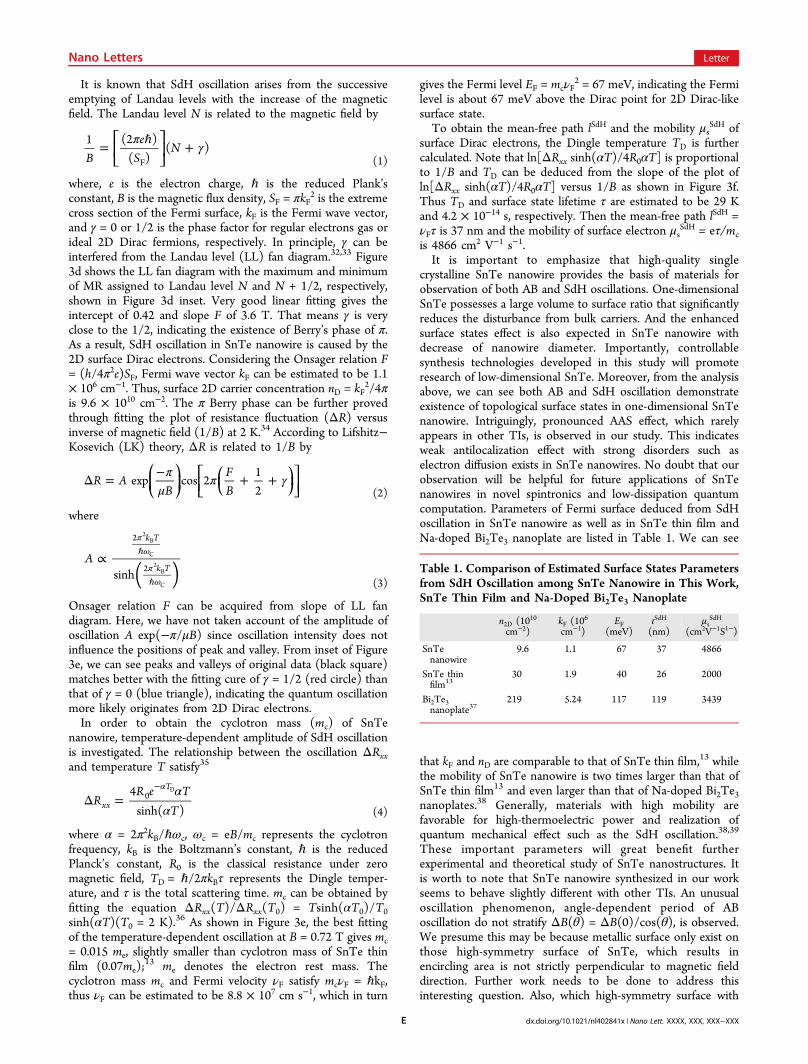
It is known that SdH oscillation arises from the successiveemptying of Landau levels with the increase of the magneticfield. The Landau level N is related to the magnetic field by
π γ= ℏ +⎡⎣⎢
⎤⎦⎥B
eS
N1 (2 )
( )( )
F (1)
where, e is the electron charge, ℏ is the reduced Plank’sconstant, B is the magnetic flux density, SF = πkF
2 is the extremecross section of the Fermi surface, kF is the Fermi wave vector,and γ = 0 or 1/2 is the phase factor for regular electrons gas orideal 2D Dirac fermions, respectively. In principle, γ can beinterfered from the Landau level (LL) fan diagram.32,33 Figure3d shows the LL fan diagram with the maximum and minimumof MR assigned to Landau level N and N + 1/2, respectively,shown in Figure 3d inset. Very good linear fitting gives theintercept of 0.42 and slope F of 3.6 T. That means γ is veryclose to the 1/2, indicating the existence of Berry’s phase of π.As a result, SdH oscillation in SnTe nanowire is caused by the2D surface Dirac electrons. Considering the Onsager relation F= (h/4π2e)SF, Fermi wave vector kF can be estimated to be 1.1× 106 cm−1. Thus, surface 2D carrier concentration nD = kF
2/4πis 9.6 × 1010 cm−2. The π Berry phase can be further provedthrough fitting the plot of resistance fluctuation (ΔR) versusinverse of magnetic field (1/B) at 2 K.34 According to Lifshitz−Kosevich (LK) theory, ΔR is related to 1/B by
πμ
π γΔ = − + +⎜ ⎟⎛⎝⎜
⎞⎠⎟
⎡⎣⎢
⎛⎝
⎞⎠⎤⎦⎥R A
BFB
exp cos 212 (2)
where
∝π
ω
πω
ℏ
ℏ( )A
sinh
k T
k T
2
2
2B
C
2B
C (3)
Onsager relation F can be acquired from slope of LL fandiagram. Here, we have not taken account of the amplitude ofoscillation A exp(−π/μB) since oscillation intensity does notinfluence the positions of peak and valley. From inset of Figure3e, we can see peaks and valleys of original data (black square)matches better with the fitting cure of γ = 1/2 (red circle) thanthat of γ = 0 (blue triangle), indicating the quantum oscillationmore likely originates from 2D Dirac electrons.In order to obtain the cyclotron mass (mc) of SnTe
nanowire, temperature-dependent amplitude of SdH oscillationis investigated. The relationship between the oscillation ΔRxxand temperature T satisfy35
αα
Δ =α−
RR e T
T4
sinh( )xx
T0
D
(4)
where α = 2π2kB/ℏωc, ωc = eB/mc represents the cyclotronfrequency, kB is the Boltzmann’s constant, ℏ is the reducedPlanck’s constant, R0 is the classical resistance under zeromagnetic field, TD = ℏ/2πkBτ represents the Dingle temper-ature, and τ is the total scattering time. mc can be obtained byfitting the equation ΔRxx(T)/ΔRxx(T0) = Tsinh(αT0)/T0sinh(αT)(T0 = 2 K).36 As shown in Figure 3e, the best fittingof the temperature-dependent oscillation at B = 0.72 T gives mc= 0.015 me, slightly smaller than cyclotron mass of SnTe thinfilm (0.07me);
13 me denotes the electron rest mass. Thecyclotron mass mc and Fermi velocity νF satisfy mcνF = ℏkF,thus νF can be estimated to be 8.8 × 107 cm s−1, which in turn
gives the Fermi level EF = mcνF2 = 67 meV, indicating the Fermi
level is about 67 meV above the Dirac point for 2D Dirac-likesurface state.To obtain the mean-free path lSdH and the mobility μs
SdH ofsurface Dirac electrons, the Dingle temperature TD is furthercalculated. Note that ln[ΔRxx sinh(αT)/4R0αT] is proportionalto 1/B and TD can be deduced from the slope of the plot ofln[ΔRxx sinh(αT)/4R0αT] versus 1/B as shown in Figure 3f.Thus TD and surface state lifetime τ are estimated to be 29 Kand 4.2 × 10⁻¹⁴ s, respectively. Then the mean-free path lSdH =νFτ is 37 nm and the mobility of surface electron μs
SdH = eτ/mcis 4866 cm2 V−1 s−1.It is important to emphasize that high-quality single
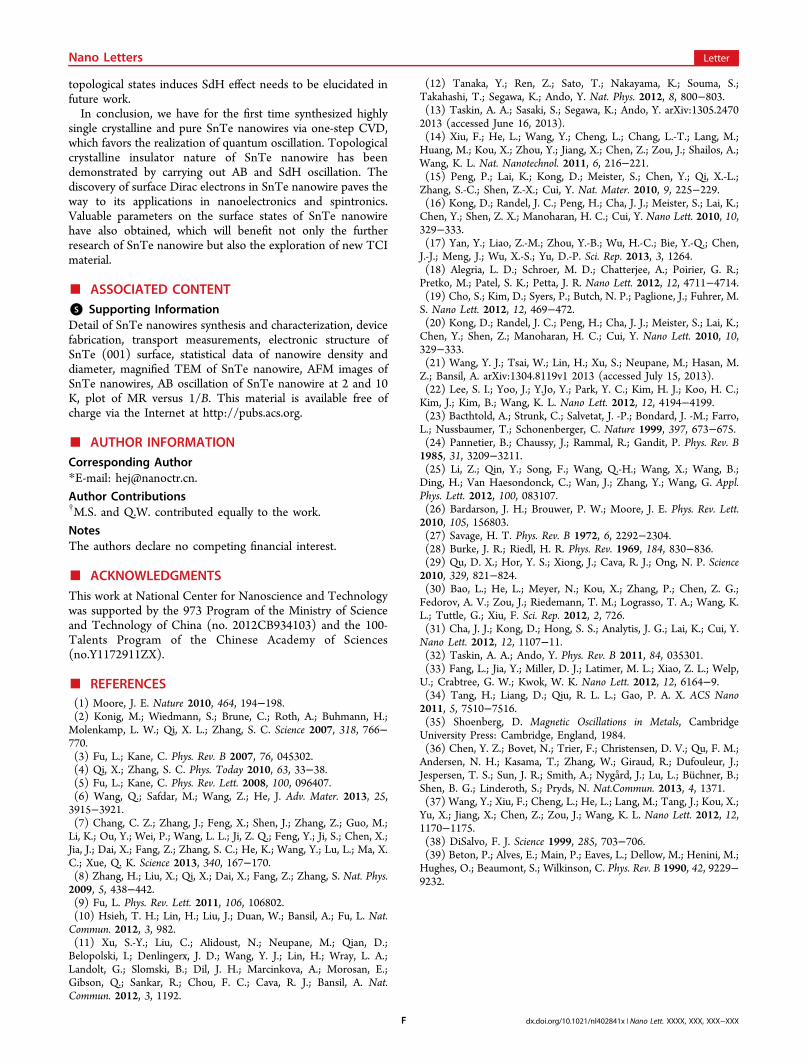
crystalline SnTe nanowire provides the basis of materials forobservation of both AB and SdH oscillations. One-dimensionalSnTe possesses a large volume to surface ratio that significantlyreduces the disturbance from bulk carriers. And the enhancedsurface states effect is also expected in SnTe nanowire withdecrease of nanowire diameter. Importantly, controllablesynthesis technologies developed in this study will promoteresearch of low-dimensional SnTe. Moreover, from the analysisabove, we can see both AB and SdH oscillation demonstrateexistence of topological surface states in one-dimensional SnTenanowire. Intriguingly, pronounced AAS effect, which rarelyappears in other TIs, is observed in our study. This indicatesweak antilocalization effect with strong disorders such aselectron diffusion exists in SnTe nanowires. No doubt that ourobservation will be helpful for future applications of SnTenanowires in novel spintronics and low-dissipation quantumcomputation. Parameters of Fermi surface deduced from SdHoscillation in SnTe nanowire as well as in SnTe thin film andNa-doped Bi2Te3 nanoplate are listed in Table 1. We can see
that kF and nD are comparable to that of SnTe thin film,13 whilethe mobility of SnTe nanowire is two times larger than that ofSnTe thin film13 and even larger than that of Na-doped Bi2Te3nanoplates.38 Generally, materials with high mobility arefavorable for high-thermoelectric power and realization ofquantum mechanical effect such as the SdH oscillation.38,39
These important parameters will great benefit furtherexperimental and theoretical study of SnTe nanostructures. Itis worth to note that SnTe nanowire synthesized in our workseems to behave slightly different with other TIs. An unusualoscillation phenomenon, angle-dependent period of ABoscillation do not stratify ΔB(θ) = ΔB(0)/cos(θ), is observed.We presume this may be because metallic surface only exist onthose high-symmetry surface of SnTe, which results inencircling area is not strictly perpendicular to magnetic fielddirection. Further work needs to be done to address thisinteresting question. Also, which high-symmetry surface with
Table 1. Comparison of Estimated Surface States Parametersfrom SdH Oscillation among SnTe Nanowire in This Work,SnTe Thin Film and Na-Doped Bi2Te3 Nanoplate
n2D (1010
cm−2)kF (10
6
cm−1)EF
(meV)ιSdH
(nm)μs
SdH
(cm2V−1S1−)
SnTenanowire
9.6 1.1 67 37 4866
SnTe thinfilm13
30 1.9 40 26 2000
Bi2Te3nanoplate37
219 5.24 117 119 3439
Nano Letters Letter
dx.doi.org/10.1021/nl402841x | Nano Lett. XXXX, XXX, XXX−XXXE
topological states induces SdH effect needs to be elucidated infuture work.In conclusion, we have for the first time synthesized highly
single crystalline and pure SnTe nanowires via one-step CVD,which favors the realization of quantum oscillation. Topologicalcrystalline insulator nature of SnTe nanowire has beendemonstrated by carrying out AB and SdH oscillation. Thediscovery of surface Dirac electrons in SnTe nanowire paves theway to its applications in nanoelectronics and spintronics.Valuable parameters on the surface states of SnTe nanowirehave also obtained, which will benefit not only the furtherresearch of SnTe nanowire but also the exploration of new TCImaterial.
■ ASSOCIATED CONTENT*S Supporting InformationDetail of SnTe nanowires synthesis and characterization, devicefabrication, transport measurements, electronic structure ofSnTe (001) surface, statistical data of nanowire density anddiameter, magnified TEM of SnTe nanowire, AFM images ofSnTe nanowires, AB oscillation of SnTe nanowire at 2 and 10K, plot of MR versus 1/B. This material is available free ofcharge via the Internet at http://pubs.acs.org.
■ AUTHOR INFORMATIONCorresponding Author*E-mail: [email protected].
Author Contributions†M.S. and Q.W. contributed equally to the work.
NotesThe authors declare no competing financial interest.
■ ACKNOWLEDGMENTSThis work at National Center for Nanoscience and Technologywas supported by the 973 Program of the Ministry of Scienceand Technology of China (no. 2012CB934103) and the 100-Talents Program of the Chinese Academy of Sciences(no.Y1172911ZX).
■ REFERENCES(1) Moore, J. E. Nature 2010, 464, 194−198.(2) Konig, M.; Wiedmann, S.; Brune, C.; Roth, A.; Buhmann, H.;Molenkamp, L. W.; Qi, X. L.; Zhang, S. C. Science 2007, 318, 766−770.(3) Fu, L.; Kane, C. Phys. Rev. B 2007, 76, 045302.(4) Qi, X.; Zhang, S. C. Phys. Today 2010, 63, 33−38.(5) Fu, L.; Kane, C. Phys. Rev. Lett. 2008, 100, 096407.(6) Wang, Q.; Safdar, M.; Wang, Z.; He, J. Adv. Mater. 2013, 25,3915−3921.(7) Chang, C. Z.; Zhang, J.; Feng, X.; Shen, J.; Zhang, Z.; Guo, M.;Li, K.; Ou, Y.; Wei, P.; Wang, L. L.; Ji, Z. Q.; Feng, Y.; Ji, S.; Chen, X.;Jia, J.; Dai, X.; Fang, Z.; Zhang, S. C.; He, K.; Wang, Y.; Lu, L.; Ma, X.C.; Xue, Q. K. Science 2013, 340, 167−170.(8) Zhang, H.; Liu, X.; Qi, X.; Dai, X.; Fang, Z.; Zhang, S. Nat. Phys.2009, 5, 438−442.(9) Fu, L. Phys. Rev. Lett. 2011, 106, 106802.(10) Hsieh, T. H.; Lin, H.; Liu, J.; Duan, W.; Bansil, A.; Fu, L. Nat.Commun. 2012, 3, 982.(11) Xu, S.-Y.; Liu, C.; Alidoust, N.; Neupane, M.; Qian, D.;Belopolski, I.; Denlingerx, J. D.; Wang, Y. J.; Lin, H.; Wray, L. A.;Landolt, G.; Slomski, B.; Dil, J. H.; Marcinkova, A.; Morosan, E.;Gibson, Q.; Sankar, R.; Chou, F. C.; Cava, R. J.; Bansil, A. Nat.Commun. 2012, 3, 1192.
(12) Tanaka, Y.; Ren, Z.; Sato, T.; Nakayama, K.; Souma, S.;Takahashi, T.; Segawa, K.; Ando, Y. Nat. Phys. 2012, 8, 800−803.(13) Taskin, A. A.; Sasaki, S.; Segawa, K.; Ando, Y. arXiv:1305.24702013 (accessed June 16, 2013).(14) Xiu, F.; He, L.; Wang, Y.; Cheng, L.; Chang, L.-T.; Lang, M.;Huang, M.; Kou, X.; Zhou, Y.; Jiang, X.; Chen, Z.; Zou, J.; Shailos, A.;Wang, K. L. Nat. Nanotechnol. 2011, 6, 216−221.(15) Peng, P.; Lai, K.; Kong, D.; Meister, S.; Chen, Y.; Qi, X.-L.;Zhang, S.-C.; Shen, Z.-X.; Cui, Y. Nat. Mater. 2010, 9, 225−229.(16) Kong, D.; Randel, J. C.; Peng, H.; Cha, J. J.; Meister, S.; Lai, K.;Chen, Y.; Shen, Z. X.; Manoharan, H. C.; Cui, Y. Nano Lett. 2010, 10,329−333.(17) Yan, Y.; Liao, Z.-M.; Zhou, Y.-B.; Wu, H.-C.; Bie, Y.-Q.; Chen,J.-J.; Meng, J.; Wu, X.-S.; Yu, D.-P. Sci. Rep. 2013, 3, 1264.(18) Alegria, L. D.; Schroer, M. D.; Chatterjee, A.; Poirier, G. R.;Pretko, M.; Patel, S. K.; Petta, J. R. Nano Lett. 2012, 12, 4711−4714.(19) Cho, S.; Kim, D.; Syers, P.; Butch, N. P.; Paglione, J.; Fuhrer, M.S. Nano Lett. 2012, 12, 469−472.(20) Kong, D.; Randel, J. C.; Peng, H.; Cha, J. J.; Meister, S.; Lai, K.;Chen, Y.; Shen, Z.; Manoharan, H. C.; Cui, Y. Nano Lett. 2010, 10,329−333.(21) Wang, Y. J.; Tsai, W.; Lin, H.; Xu, S.; Neupane, M.; Hasan, M.Z.; Bansil, A. arXiv:1304.8119v1 2013 (accessed July 15, 2013).(22) Lee, S. I.; Yoo, J.; Y.Jo, Y.; Park, Y. C.; Kim, H. J.; Koo, H. C.;Kim, J.; Kim, B.; Wang, K. L. Nano Lett. 2012, 12, 4194−4199.(23) Bacthtold, A.; Strunk, C.; Salvetat, J. -P.; Bondard, J. -M.; Farro,L.; Nussbaumer, T.; Schonenberger, C. Nature 1999, 397, 673−675.(24) Pannetier, B.; Chaussy, J.; Rammal, R.; Gandit, P. Phys. Rev. B1985, 31, 3209−3211.(25) Li, Z.; Qin, Y.; Song, F.; Wang, Q.-H.; Wang, X.; Wang, B.;Ding, H.; Van Haesondonck, C.; Wan, J.; Zhang, Y.; Wang, G. Appl.Phys. Lett. 2012, 100, 083107.(26) Bardarson, J. H.; Brouwer, P. W.; Moore, J. E. Phys. Rev. Lett.2010, 105, 156803.(27) Savage, H. T. Phys. Rev. B 1972, 6, 2292−2304.(28) Burke, J. R.; Riedl, H. R. Phys. Rev. 1969, 184, 830−836.(29) Qu, D. X.; Hor, Y. S.; Xiong, J.; Cava, R. J.; Ong, N. P. Science2010, 329, 821−824.(30) Bao, L.; He, L.; Meyer, N.; Kou, X.; Zhang, P.; Chen, Z. G.;Fedorov, A. V.; Zou, J.; Riedemann, T. M.; Lograsso, T. A.; Wang, K.L.; Tuttle, G.; Xiu, F. Sci. Rep. 2012, 2, 726.(31) Cha, J. J.; Kong, D.; Hong, S. S.; Analytis, J. G.; Lai, K.; Cui, Y.Nano Lett. 2012, 12, 1107−11.(32) Taskin, A. A.; Ando, Y. Phys. Rev. B 2011, 84, 035301.(33) Fang, L.; Jia, Y.; Miller, D. J.; Latimer, M. L.; Xiao, Z. L.; Welp,U.; Crabtree, G. W.; Kwok, W. K. Nano Lett. 2012, 12, 6164−9.(34) Tang, H.; Liang, D.; Qiu, R. L. L.; Gao, P. A. X. ACS Nano2011, 5, 7510−7516.(35) Shoenberg, D. Magnetic Oscillations in Metals, CambridgeUniversity Press: Cambridge, England, 1984.(36) Chen, Y. Z.; Bovet, N.; Trier, F.; Christensen, D. V.; Qu, F. M.;Andersen, N. H.; Kasama, T.; Zhang, W.; Giraud, R.; Dufouleur, J.;Jespersen, T. S.; Sun, J. R.; Smith, A.; Nygard, J.; Lu, L.; Buchner, B.;Shen, B. G.; Linderoth, S.; Pryds, N. Nat.Commun. 2013, 4, 1371.(37) Wang, Y.; Xiu, F.; Cheng, L.; He, L.; Lang, M.; Tang, J.; Kou, X.;Yu, X.; Jiang, X.; Chen, Z.; Zou, J.; Wang, K. L. Nano Lett. 2012, 12,1170−1175.(38) DiSalvo, F. J. Science 1999, 285, 703−706.(39) Beton, P.; Alves, E.; Main, P.; Eaves, L.; Dellow, M.; Henini, M.;Hughes, O.; Beaumont, S.; Wilkinson, C. Phys. Rev. B 1990, 42, 9229−9232.
Nano Letters Letter
dx.doi.org/10.1021/nl402841x | Nano Lett. XXXX, XXX, XXX−XXXF
Related Documents


