2008 C2 1 2 3 4 6 8 10 14 16 17 18 20 目次 CONTENTS TOKYO ELECTRON As of March 31, 2008 FACT BOOK Industry Data インダストリー・データ Tokyo Electron (TEL) Overview 東京エレクトロン(TEL)の事業概要 Global TEL TELの世界展開 Topics in Recent Years 近年のトピックス Semiconductor & TFT-LCD Manufacturing Process Flow 半導体製造工程及び TFT-LCD製造工程 Consolidated Operating Results 連結業績 Semiconductor Production Equipment (SPE) and FPD Production Equipment 半導体製造装置・FPD製造装置 Consolidated Financial Data 連結財務データ Consolidated Balance Sheets 連結貸借対照表 Consolidated Statements of Operations 連結損益計算書 Consolidated Statements of Cash Flows 連結キャッシュ・フロー計算書 Consolidated Quarterly Data 連結四半期データ Stock Information 株式情報

Welcome message from author
This document is posted to help you gain knowledge. Please leave a comment to let me know what you think about it! Share it to your friends and learn new things together.
Transcript
2008
TOKYO ELECTRON LIMITED
World Headquarters
Akasaka Biz Tower 3-1, Akasaka 5-chomeMinato-ku, Tokyo 107-6325, JapanTel: +81-3-5561-7000Fax: +81-3-5561-7400 URL: http://www.tel.com
Investor RelationsCorporate Communications Dept.
Tel: +81-3-5561-7003Fax: +81-3-5561-7400
C2
1
2
3
4
6
8
10
14
16
17
18
20
目次CONTENTS
TOKYO ELECTRON
As o f March 31 , 2008
FACTBOOK
PR46-133Printed in Japan
本誌は再生紙を使用しています。Printed on recycled paper.
Industry Data インダストリー・データ
Tokyo Electron (TEL) Overview東京エレクトロン(TEL)の事業概要
Global TELTELの世界展開
Topics in Recent Years近年のトピックス
Semiconductor & TFT-LCD Manufacturing Process Flow
半導体製造工程及びTFT-LCD製造工程
Consolidated Operating Results連結業績
Semiconductor Production Equipment (SPE) and
FPD Production Equipment半導体製造装置・FPD製造装置
Consolidated Financial Data連結財務データ
Consolidated Balance Sheets連結貸借対照表
Consolidated Statements of Operations連結損益計算書
Consolidated Statements of Cash Flows連結キャッシュ・フロー計算書
Consolidated Quarterly Data連結四半期データ
Stock Information株式情報
010_0454002472006.indd 2 2008/07/11 16:38:13
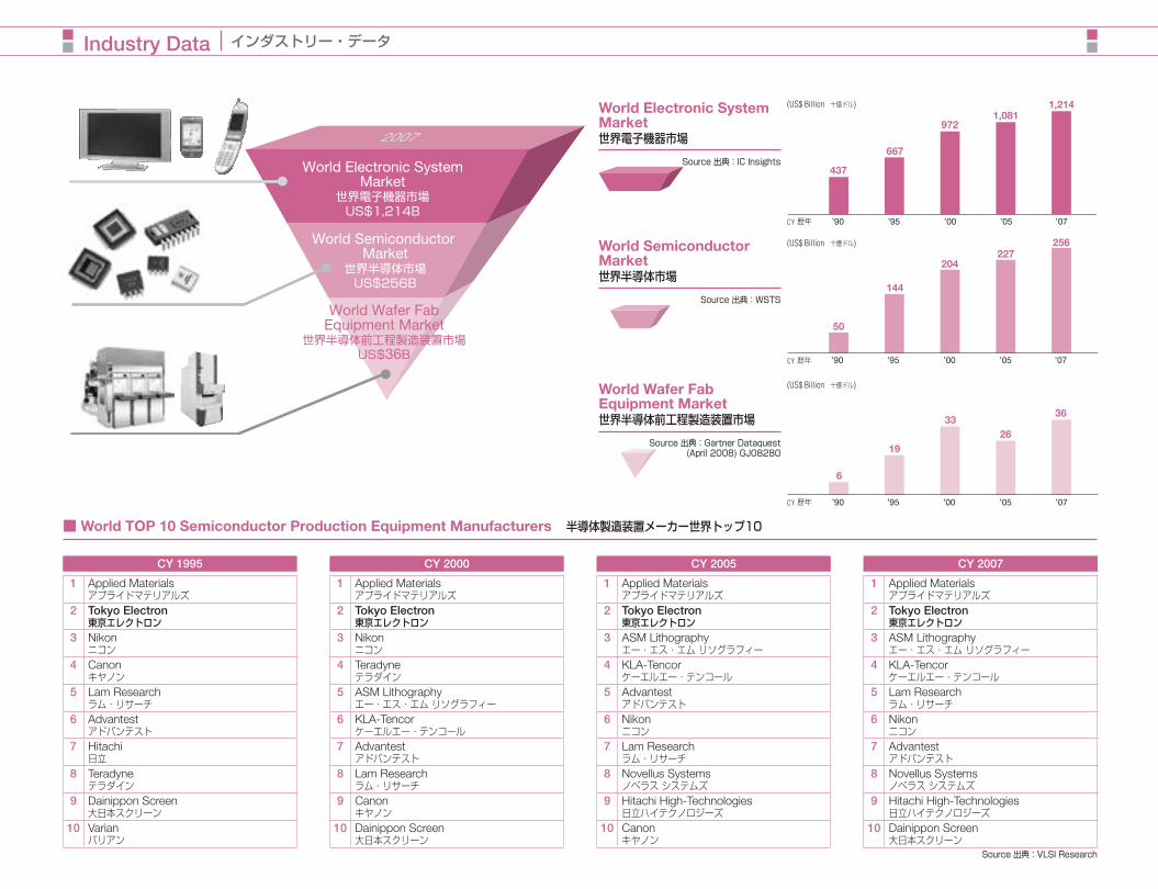
Industry Data インダストリー・データ
■ World TOP 10 Semiconductor Production Equipment Manufacturers 半導体製造装置メーカー世界トップ10
CY 2000
1 Applied Materialsアプライドマテリアルズ
2 Tokyo Electron東京エレクトロン
3 Nikonニコン
4 Teradyneテラダイン
5 ASM Lithographyエー・エス・エム リソグラフィー
6 KLA-Tencorケーエルエー・テンコール
7 Advantestアドバンテスト
8 Lam Researchラム・リサーチ
9 Canonキヤノン
10 Dainippon Screen大日本スクリーン
CY 2005
1 Applied Materialsアプライドマテリアルズ
2 Tokyo Electron東京エレクトロン
3 ASM Lithographyエー・エス・エム リソグラフィー
4 KLA-Tencorケーエルエー・テンコール
5 Advantestアドバンテスト
6 Nikonニコン
7 Lam Researchラム・リサーチ
8 Novellus Systemsノベラス システムズ
9 Hitachi High-Technologies日立ハイテクノロジーズ
10 Canonキヤノン
CY 2007
1 Applied Materialsアプライドマテリアルズ
2 Tokyo Electron東京エレクトロン
3 ASM Lithographyエー・エス・エム リソグラフィー
4 KLA-Tencorケーエルエー・テンコール
5 Lam Researchラム・リサーチ
6 Nikonニコン
7 Advantestアドバンテスト
8 Novellus Systemsノベラス システムズ
9 Hitachi High-Technologies日立ハイテクノロジーズ
10 Dainippon Screen大日本スクリーン
World Electronic SystemMarket
世界電子機器市場US$1,214B
World Semiconductor Market
世界半導体市場US$256B
World Wafer FabEquipment Market
世界半導体前工程製造装置市場US$36B
2007
1,214(US$ Billion 十億ドル)
CY 歴年 ’90 ’95 ’00 ’07’05
437
667
9721,081
World Electronic System Market世界電子機器市場
Source 出典:IC Insights
256(US$ Billion 十億ドル)
CY 歴年
50
144
204
’90 ’95 ’00 ’07’05
227World Semiconductor Market世界半導体市場
Source 出典:WSTS
36
(US$ Billion 十億ドル)
CY 歴年 ’90 ’95 ’00 ’05 ’07
6
19
3326
World Wafer Fab Equipment Market世界半導体前工程製造装置市場
Source 出典:Gartner Dataquest (April 2008) GJ08280
Source 出典:VLSI Research
CY 1995
1 Applied Materialsアプライドマテリアルズ
2 Tokyo Electron東京エレクトロン
3 Nikonニコン
4 Canonキヤノン
5 Lam Researchラム・リサーチ
6 Advantestアドバンテスト
7 Hitachi日立
8 Teradyneテラダイン
9 Dainippon Screen大日本スクリーン
10 Varianバリアン
010_0454002472006.indd 3 2008/07/11 16:38:14
1
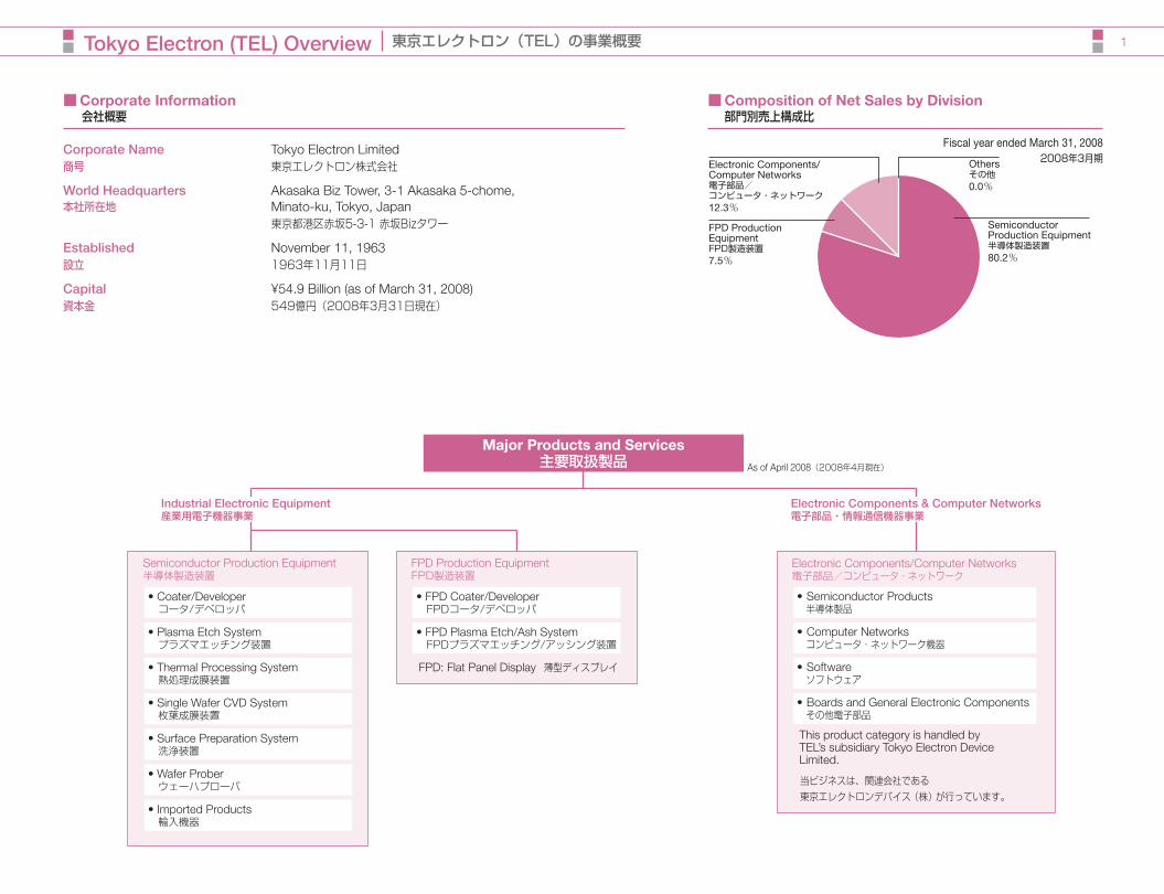
■ Corporate Information 会社概要
Tokyo Electron (TEL) Overview 東京エレクトロン(TEL)の事業概要
■ Composition of Net Sales by Division 部門別売上構成比
Fiscal year ended March 31, 20082008年3月期
Semiconductor Production Equipment 半導体製造装置80.2%
Electronic Components/Computer Networks電子部品/コンピュータ・ネットワーク12.3%
Othersその他0.0%
FPD ProductionEquipmentFPD製造装置7.5%
Corporate Name Tokyo Electron Limited商号 東京エレクトロン株式会社 World Headquarters Akasaka Biz Tower, 3-1 Akasaka 5-chome,本社所在地 Minato-ku, Tokyo, Japan 東京都港区赤坂5-3-1 赤坂Bizタワー Established November 11, 1963 設立 1963年11月11日 Capital ¥54.9 Billion (as of March 31, 2008) 資本金 549億円(2008年3月31日現在)
Major Products and Services主要取扱製品
Semiconductor Production Equipment半導体製造装置
• Imported Products 輸入機器
As of April 2008(2008年4月現在)
Industrial Electronic Equipment産業用電子機器事業
Electronic Components & Computer Networks電子部品・情報通信機器事業
�• Coater/Developer コータ/デベロッパ
�• Plasma Etch System プラズマエッチング装置
• Thermal Processing System 熱処理成膜装置
• Single Wafer CVD System 枚葉成膜装置
• Surface Preparation System 洗浄装置
• Wafer Prober ウェーハプローバ
FPD Production EquipmentFPD製造装置
FPD: Flat Panel Display 薄型ディスプレイ
• FPD Coater/Developer FPDコータ/デベロッパ
• FPD Plasma Etch/Ash System FPDプラズマエッチング/アッシング装置
This product category is handled by TEL’s subsidiary Tokyo Electron Device Limited.
当ビジネスは、関連会社である東京エレクトロンデバイス(株)が行っています。
•�Software ソフトウェア
•�Boards and General Electronic Components その他電子部品
•�Computer Networks コンピュータ・ネットワーク機器
•�Semiconductor Products 半導体製品
Electronic Components/Computer Networks電子部品/コンピュータ・ネットワーク
010_0454002472006.indd 1 2008/07/11 16:38:15
2
• Tokyo Electron Ltd. 東京エレクトロン
• Tokyo Electoron Device Ltd. 東京エレクトロンデバイス
• Tokyo Electron FE Ltd. 東京エレクトロンFE
• Tokyo Electron PS Ltd. 東京エレクトロンPS
• Tokyo Electron Korea Ltd.
• Tokyo Electron Korea Solution Ltd.
• Tokyo Electron Taiwan Ltd.
• Tokyo Electron (Shanghai) Ltd.
• Tokyo Electron America, Inc.
• Tokyo Electron Europe. Ltd.
• Tokyo Electron Israel Ltd.
• Tokyo Electron AT Ltd. 東京エレクトロンAT
• Tokyo Electoron Kyushu Ltd. 東京エレクトロン九州
• Tokyo Electoron Tohoku Ltd. 東京エレクトロン東北
• Tokyo Electron Massachusetts, LLC
• TEL Epion, Inc.
• Timbre Technologies, Inc.
• Tokyo Electron TS Ltd. 東京エレクトロンTS
• Tokyo Electoron Software Technologies Ltd. 東京エレクトロン ソフトウェア・テクノロジーズ
• Tokyo Electron Ltd. 東京エレクトロン
• Tokyo Electoron Technology Development Institute, Inc. 東京エレクトロン技術研究所
• Tokyo Electron PV Ltd. 東京エレクトロンPV
• TEL Technology Center, America, LLC • Tokyo Electron U.S. Holdings, Inc.
• TEL Venture Capital, Inc.
• Tokyo Electoron BP Ltd. 東京エレクトロンBP
• Tokyo Electron Agency Ltd. 東京エレクトロンエージェンシー
Othersその他
Research/Development研究・開発
Field Supportフィールドサポート
Manufacturing/Development製造・開発
Sales/Marketingセールス・マーケティング
Global TEL TELの世界展開
0
250,000
500,000
750,000
1000,000
Sales in Japan 国内売上高 Sales Overseas 海外売上高
2006 2007 20081998 1999 2000 2001 2002 2003 2004 2005
(¥ Millions 百万円)
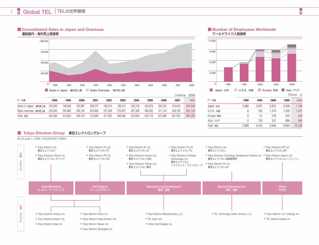
FY 年度 1998 1999 2000 2001 2002 2003 2004 2005 2006 2007 2008
Sales in Japan 国内売上高 230,550 149,838 183,987 299,272 186,516 190,513 242,318 232,678 262,532 313,816 323,946Sales overseas 海外売上高 225,035 163,982 256,742 424,608 231,309 270,067 287,336 403,032 411,154 538,159 582,146
Total 合計 455,585 313,820 440,729 723,880 417,825 460,580 529,654 635,710 673,686 851,975 906,092
■ Consolidated Sales in Japan and Overseas 連結国内・海外売上高推移
■ Number of Employees Worldwide ワールドワイド人員推移
■ Tokyo Electron Group 東京エレクトロングループAs of June 1, 2008(2008年6月1日現在)
1990 1995 2000 20050
3,000
6,000
9,000
12,000
Japan 日本 U.S.A. 米国 Europe 欧州 Asia アジア
2008
(Persons 人)
FY 年度 1990 1995 2000 2005 2008
Japan 日本 3,980 5,041 6,922 6,548 7,789U.S.A. 米国 8 192 1,315 1,205 1,281Europe 欧州 0 51 378 425 450Asia アジア 0 126 331 686 909Total 合計 3,988 5,410 8,946 8,864 10,429
Dom
estic
国
内 O
vers
eas
海外
010_0454002472006.indd 2 2008/07/11 16:38:15

3Topics in Recent Years 近年のトピックス
8月Aug
TEL Technology Center, America, LLC (TTCA) established in the U.S. to conduct research and development of cutting-edge semiconductor materials and processes.
米国に先進的な半導体材料およびプロセスの研究を行うTEL Technology Center, America, LLC (TTCA)を設立
2004 4月Apr
Tokyo Electron AT Ltd. (surviving company) and Tokyo Electron Tohoku Ltd., manufacturing subsidiaries in Japan, merged.
国内製造拠点、東京エレクトロンAT(株)(存続会社)と東京エレクトロン東北(株)が合併
7月Jul
Tokyo Electron U.S. Holdings, Inc. established in the U.S. It controls Tokyo Electron America, Tokyo Electron Massachusetts and TEL Technology Center, America.
米国に持株会社Tokyo Electron U.S. Holdings, Inc.を設立。米国内現地法人Tokyo Electron America, Tokyo Electron Massachusetts, TEL Technology Center, Americaを傘下に入れる。
2005 1月Jan
TEL received the Superior Corporate Disclosure Award from the Tokyo Stock Exchange for the second time, the first time being in 1999.
東証より、1999年に引き続き2度目の「ディスクロージャー優良企業」に選定され、受賞
2006 2月Feb
Tokyo Electron Korea Solution Ltd. established.
東京エレクトロンコリアソリューション(株)を設立
4月Apr
Tokyo Electron AT was split into three- Tokyo Electron At Ltd., Tokyo Electron Tohoku Ltd. and Tokyo Electron TS Ltd.
東京エレクトロンAT(株)を分割し、東京エレクトロンAT(株)、東京エレクトロン東北
(株)、東京エレクトロンTS(株)を設立
6月Jun
TEL Venture Capital, Inc. established
米国にTEL Venture Capital, Inc.を設立
12月Dec
TEL acquired Epion Corporation, a supplier of gas cluster ion beam technology.
ガスクラスターイオンビーム技術を有する米国・エピオン社を買収
2007
2月Feb
Tokyo Electron PS Ltd. established.
ポストセールス専門のエンジニアリング会社・東京エレクトロンPS(株)を設立
6月Jun
RLSA Division spun off and Tokyo Electron Technology Development Institute, Inc. established.
RLSA事業部門を分社化し、東京エレクトロン技術研究所(株)を設立
11月Nov
TEL joined leading chip-makers in SEMATECH's 3D Interconnect Program.
SEMATECH三次元積層プログラムに参加
2008 2月Feb
TEL entered the photovoltaic cell production equipment business.
薄膜シリコン型太陽電池用製造装置事業に参入
1998 2月Feb
Construction of a new facility at the Process Technology Center capable of handling 300mm wafer was completed in Hosaka, Yamanashi Prefecture.
山梨穂坂地区に300mmウェーハ対応プロセステクノロジーセンター新棟が完成
1999 10月Oct
TEL's sector classification in the First Section of the Tokyo Stock Exchange was changed from "Wholesale Trade" to "Electric Appliances".
東証第1部における業種を「商業」から「電気機器」へ変更
2000 8月Aug
The trading unit for TEL stock was changed from 1,000 shares to 100 shares.
1単位の株式数を1,000株から100株に変更
2001 2月Feb
TEL acquired a stake in Timbre Technologies, Inc., a leader in advanced metrology.
最先端の計測ソフトウェア技術を有する米国Timbre Technologies, Inc.を買収し子会社にする
2002 4月Apr
Tokyo Electron (Shanghai) Ltd. established.
東京エレクトロン上海(株)を設立
11月Nov
TEL participated in Albany NanoTech project promoted by New York State.
ニューヨーク州が推進する研究開発推進支援プログラム「アルバニー・ナノテック」プロジェクトへ参加
2003 3月Mar
Tokyo Electron Device Ltd. listed on the 2nd Section of the Tokyo Stock Exchange.
東京エレクトロンデバイス(株)東京証券取引所第2部に上場
010_0454002472006.indd 3 2008/07/11 16:38:15
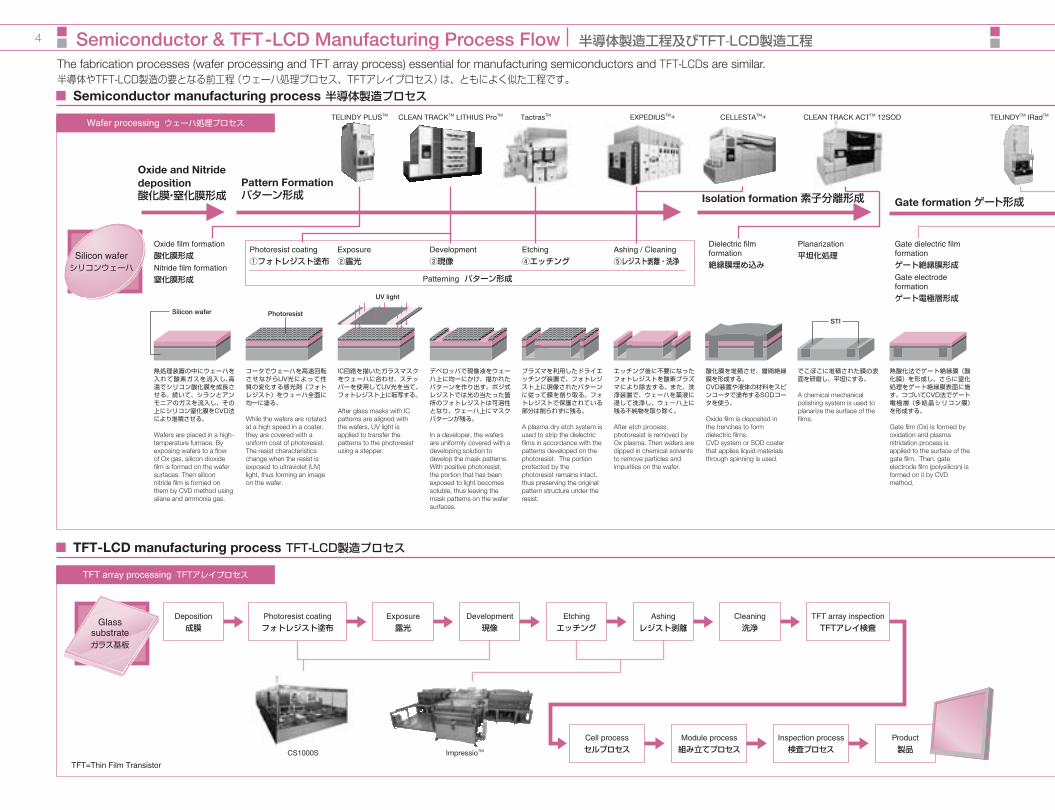
4 Semiconductor & TFT-LCD Manufacturing Process Flow 半導体製造工程及びTFT-LCD製造工程
Semiconductor manufacturing process 半導体製造プロセス
Interconnect formation 配線形成
Cross section 断面図
Wafer testウェーハ検査
Wafer processing ウェーハ処理プロセス
TFT array processing TFTアレイプロセス
ゲート電極層上にパターン形成プロセスを施し、ソース・ドレイン領域をつくる。
Source and drain areas are made by applying patterning processes to the gate electrode layer.
Photoresist coating
フォトレジスト塗布Exposure
露光Development
現像Etching
エッチングAshing
レジスト剥離Cleaning
洗浄TFT array inspection
TFTアレイ検査
Cell process
セルプロセスModule process
組み立てプロセスInspection process
検査プロセスProduct
製品
ソース・ドレイ領域にイオン注入法で導入した元素(ホウ素や砒素等)を打ち込む。酸化膜が残っている部分にはイオンが注入されない。その後、高温アニールによって不純物を均一に拡散させる。
An ion implanter dopes the source and drain areas with impurities, such as boron and arsenic. Ox films prevent dopant ions from being implanted in other areas. Subsequent annealing diffuses these impurities to a more uniform density.
酸化膜をCVD法で堆積させ層間絶縁膜を形成し、表面を研磨して平坦にする。
Intermetal dielectric film is formed by oxide using CVD method and the film surface is planarized by polishing system subsequently.
絶縁膜上にパターン形成プロセスを施し、コンタクトホールを開口する。
Contact holes are opened by applying patterning processes to the dielectric film surface.
CVD法で金属膜を埋め込む。余分な膜は研磨で除去する
The holes are filled with metal film by CVD, then excess metal is removed by polishing.
低誘電率膜等の層間絶縁膜を堆積する。次にパターン形成を行い配線となる部分(トレンチ)を開口する
Low-dielectric-constant film is deposited followed by trench formation in the film by patterning process.
トレンチに金属膜を埋め込み余分な膜を研磨し除去する。
Metal films are filled into the trench and excess metals are polished.
層間絶縁膜堆積~金属膜埋め込み/研磨の一連のプロセスを必要な配線層数分繰り返す
Processes from dielectricfilm formation to metalpolishing are repeated tomake a multi level inter-connect.
でき上がったウェーハには同じLSIチップが数百個作られている。プローバで1つ1つのチップにプローブ針を接触させ、つないだテスターと信号のやりとりをしながらチップの良・不良を電気的に検査する。
There are several hundreds of identical LSI chips on a fabricated wafer. Prober makes pins contact chips, and tests whether chips are good or bad electrically by exchanging signals.
Photoresist coating
①フォトレジスト塗布
Oxide film formation
酸化膜形成Nitride film formation
窒化膜形成
Exposure
②露光Development
③現像Etching
④エッチングAshing / Cleaning
⑤レジスト剥離・洗浄
Dielectric filmformation
絶縁膜埋め込み
Planarization
平坦化処理Gate dielectric filmformation
ゲート絶縁膜形成Gate electrodeformation
ゲート電極層形成
Patterning
パターン形成Patterning
パターン形成Patterning
パターン形成
Ion implantation
イオン注入Annealing
アニール
Intermetal dielectric film formation
層間絶縁膜形成Planarization
平坦化処理
Probe Testing
プローブ検査
Assembly process
組立プロセス
Contact formation
コンタクト形成Interconnect formation
配線形成
Inspection process
検査プロセス
Product
製 品
Patterning パターン形成
Deposition
成膜
TFT=Thin Film Transistor
UV lightUV lightUV light
impurities
Bac
k lig
ht
ITO
ITO
Pol
ariz
er F
ilter
Alig
nmen
t Lay
er
Liqu
id C
ryst
al
Alig
nmen
t Lay
erIT
O E
lect
rode
Ove
r C
oat
GB
BM
BM
BM
R
Gla
ss(C
olor
Filt
er S
ide)
Gla
ss(T
FT
Arr
ay S
ide)
Pol
ariz
er F
ilter
ITO
TF
TT
FT
TF
T
Side View of TFT-LCD panel
Color Filter TFT Array Substrate
PhotoresistPhotoresist Photoresist
ImpressioTM
CLEAN TRACKTM LITHIUS ProTM TactrasTM EXPEDIUSTM+ TriasTM SPA / TriasTM High-k CVD TriasTM PrecioTMTELFORMULATMTELINDYTM IRadTMCELLESTATM+TELINDY PLUSTM
CS1000S
Gate formation ゲート形成
STI
Glasssubstrateガラス基板
CLEAN TRACK ACTTM 12SOD
Isolation formation 素子分離形成Pattern Formationパターン形成
Oxide and Nitride deposition酸化膜・窒化膜形成
DRAM Logic
TFT-LCD manufacturing process TFT-LCD製造プロセス
熱処理装置の中にウェーハを入れて酸素ガスを流入し、高温でシリコン酸化膜を成長させる。続いて、シランとアンモニアのガスを流入し、その上にシリコン窒化膜をCVD法により堆積させる。
Wafers are placed in a high- temperature furnace. By exposing wafers to a flow of Ox gas, silicon dioxide film is formed on the wafer surfaces. Then silicon nitride film is formed on them by CVD method using silane and ammonia gas.
コータでウェーハを高速回転させながらUV光によって性質の変化する感光剤(フォトレジスト)をウェーハ全面に均一に塗る。
While the wafers are rotated at a high speed in a coater, they are covered with a uniform coat of photoresist. The resist characteristics change when the resist is exposed to ultraviolet (UV) light, thus forming an image on the wafer.
IC回路を描いたガラスマスクをウェーハに合わせ、ステッパーを使用してUV光を当て、フォトレジスト上に転写する。
After glass masks with IC patterns are aligned with the wafers, UV light is applied to transfer the patterns to the photoresist using a stepper.
デベロッパで現像液をウェーハ上に均一にかけ、描かれたパターンを作り出す。ポジ式レジストでは光の当たった箇所のフォトレジストは可溶性となり、ウェーハ上にマスクパターンが残る。
In a developer, the wafers are uniformly covered with a developing solution to develop the mask patterns. With positive photoresist, the portion that has been exposed to light becomes soluble, thus leaving the mask patterns on the wafer surfaces.
プラズマを利用したドライエッチング装置で、フォトレジスト上に現像されたパターンに従って膜を削り取る。フォトレジストで保護されている部分は削られずに残る。
A plasma dry etch system is used to strip the dielectric films in accordance with the patterns developed on the photoresist. The portion protected by the photoresist remains intact, thus preserving the original pattern structure under the resist.
エッチング後に不要になったフォトレジストを酸素プラズマにより除去する。また、洗浄装置で、ウェーハを薬液に浸して洗浄し、ウェーハ上に残る不純物を取り除く。
After etch process, photoresist is removed by Ox plasma. Then wafers are dipped in chemical solvents to remove particles and impurities on the wafer.
酸化膜を堆積させ、層間絶縁膜を形成する。CVD装置や液体の材料をスピンコータで塗布するSODコータを使う。
Oxide film is deposited in the trenches to form dielectric films.CVD system or SOD coater that applies liquid materials through spinning is used.
でこぼこに堆積された膜の表面を研磨し、平坦にする。
A chemical mechanical polishing system is used to planarize the surface of the films.
熱酸化法でゲート絶縁膜(酸化膜)を形成し、さらに窒化処理をゲート絶縁膜表面に施す。つづいてCVD法でゲート電極層(多結晶シリコン膜)を形成する。
Gate film (Ox) is formed by oxidation and plasma nitridation process is applied to the surface of the gate film. Then, gate electrode film (polysilicon) is formed on it by CVD method.
Silicon waferシリコンウェーハ
UV light
PhotoresistSilicon wafer
Interconnect配線
Inter Layer Dielectric層間絶縁膜
Contactコンタクト
Gateゲート
Source/Drainソース/ドレイン
Capacitorキャパシタ
Source/Drainソース/ドレイン
STI素子分離
The fabrication processes (wafer processing and TFT array process) essential for manufacturing semiconductors and TFT-LCDs are similar.半導体やTFT-LCD製造の要となる前工程(ウェーハ処理プロセス、TFTアレイプロセス)は、ともによく似た工程です。
010_0454002472006.indd 4 2008/07/11 16:38:20

5
Semiconductor manufacturing process 半導体製造プロセス
Interconnect formation 配線形成
Cross section 断面図
Wafer testウェーハ検査
Wafer processing ウェーハ処理プロセス
TFT array processing TFTアレイプロセス
ゲート電極層上にパターン形成プロセスを施し、ソース・ドレイン領域をつくる。
Source and drain areas are made by applying patterning processes to the gate electrode layer.
Photoresist coating
フォトレジスト塗布Exposure
露光Development
現像Etching
エッチングAshing
レジスト剥離Cleaning
洗浄TFT array inspection
TFTアレイ検査
Cell process
セルプロセスModule process
組み立てプロセスInspection process
検査プロセスProduct
製品
ソース・ドレイ領域にイオン注入法で導入した元素(ホウ素や砒素等)を打ち込む。酸化膜が残っている部分にはイオンが注入されない。その後、高温アニールによって不純物を均一に拡散させる。
An ion implanter dopes the source and drain areas with impurities, such as boron and arsenic. Ox films prevent dopant ions from being implanted in other areas. Subsequent annealing diffuses these impurities to a more uniform density.
酸化膜をCVD法で堆積させ層間絶縁膜を形成し、表面を研磨して平坦にする。
Intermetal dielectric film is formed by oxide using CVD method and the film surface is planarized by polishing system subsequently.
絶縁膜上にパターン形成プロセスを施し、コンタクトホールを開口する。
Contact holes are opened by applying patterning processes to the dielectric film surface.
CVD法で金属膜を埋め込む。余分な膜は研磨で除去する
The holes are filled with metal film by CVD, then excess metal is removed by polishing.
低誘電率膜等の層間絶縁膜を堆積する。次にパターン形成を行い配線となる部分(トレンチ)を開口する
Low-dielectric-constant film is deposited followed by trench formation in the film by patterning process.
トレンチに金属膜を埋め込み余分な膜を研磨し除去する。
Metal films are filled into the trench and excess metals are polished.
層間絶縁膜堆積~金属膜埋め込み/研磨の一連のプロセスを必要な配線層数分繰り返す
Processes from dielectricfilm formation to metalpolishing are repeated tomake a multi level inter-connect.
でき上がったウェーハには同じLSIチップが数百個作られている。プローバで1つ1つのチップにプローブ針を接触させ、つないだテスターと信号のやりとりをしながらチップの良・不良を電気的に検査する。
There are several hundreds of identical LSI chips on a fabricated wafer. Prober makes pins contact chips, and tests whether chips are good or bad electrically by exchanging signals.
Photoresist coating
①フォトレジスト塗布
Oxide film formation
酸化膜形成Nitride film formation
窒化膜形成
Exposure
②露光Development
③現像Etching
④エッチングAshing / Cleaning
⑤レジスト剥離・洗浄
Dielectric filmformation
絶縁膜埋め込み
Planarization
平坦化処理Gate dielectric filmformation
ゲート絶縁膜形成Gate electrodeformation
ゲート電極層形成
Patterning
パターン形成Patterning
パターン形成Patterning
パターン形成
Ion implantation
イオン注入Annealing
アニール
Intermetal dielectric film formation
層間絶縁膜形成Planarization
平坦化処理
Probe Testing
プローブ検査
Assembly process
組立プロセス
Contact formation
コンタクト形成Interconnect formation
配線形成
Inspection process
検査プロセス
Product
製 品
Patterning パターン形成
Deposition
成膜
TFT=Thin Film Transistor
UV lightUV lightUV light
impurities
Bac
k lig
ht
ITO
ITO
Pol
ariz
er F
ilter
Alig
nmen
t Lay
er
Liqu
id C
ryst
al
Alig
nmen
t Lay
erIT
O E
lect
rode
Ove
r C
oat
GB
BM
BM
BM
R
Gla
ss(C
olor
Filt
er S
ide)
Gla
ss(T
FT
Arr
ay S
ide)
Pol
ariz
er F
ilter
ITO
TF
TT
FT
TF
T
Side View of TFT-LCD panel
Color Filter TFT Array Substrate
PhotoresistPhotoresist Photoresist
ImpressioTM
CLEAN TRACKTM LITHIUS ProTM TactrasTM EXPEDIUSTM+ TriasTM SPA / TriasTM High-k CVD TriasTM PrecioTMTELFORMULATMTELINDYTM IRadTMCELLESTATM+TELINDY PLUSTM
CS1000S
Gate formation ゲート形成
STI
Glasssubstrateガラス基板
CLEAN TRACK ACTTM 12SOD
Isolation formation 素子分離形成Pattern Formationパターン形成
Oxide and Nitride deposition酸化膜・窒化膜形成
DRAM Logic
TFT-LCD manufacturing process TFT-LCD製造プロセス
熱処理装置の中にウェーハを入れて酸素ガスを流入し、高温でシリコン酸化膜を成長させる。続いて、シランとアンモニアのガスを流入し、その上にシリコン窒化膜をCVD法により堆積させる。
Wafers are placed in a high- temperature furnace. By exposing wafers to a flow of Ox gas, silicon dioxide film is formed on the wafer surfaces. Then silicon nitride film is formed on them by CVD method using silane and ammonia gas.
コータでウェーハを高速回転させながらUV光によって性質の変化する感光剤(フォトレジスト)をウェーハ全面に均一に塗る。
While the wafers are rotated at a high speed in a coater, they are covered with a uniform coat of photoresist. The resist characteristics change when the resist is exposed to ultraviolet (UV) light, thus forming an image on the wafer.
IC回路を描いたガラスマスクをウェーハに合わせ、ステッパーを使用してUV光を当て、フォトレジスト上に転写する。
After glass masks with IC patterns are aligned with the wafers, UV light is applied to transfer the patterns to the photoresist using a stepper.
デベロッパで現像液をウェーハ上に均一にかけ、描かれたパターンを作り出す。ポジ式レジストでは光の当たった箇所のフォトレジストは可溶性となり、ウェーハ上にマスクパターンが残る。
In a developer, the wafers are uniformly covered with a developing solution to develop the mask patterns. With positive photoresist, the portion that has been exposed to light becomes soluble, thus leaving the mask patterns on the wafer surfaces.
プラズマを利用したドライエッチング装置で、フォトレジスト上に現像されたパターンに従って膜を削り取る。フォトレジストで保護されている部分は削られずに残る。
A plasma dry etch system is used to strip the dielectric films in accordance with the patterns developed on the photoresist. The portion protected by the photoresist remains intact, thus preserving the original pattern structure under the resist.
エッチング後に不要になったフォトレジストを酸素プラズマにより除去する。また、洗浄装置で、ウェーハを薬液に浸して洗浄し、ウェーハ上に残る不純物を取り除く。
After etch process, photoresist is removed by Ox plasma. Then wafers are dipped in chemical solvents to remove particles and impurities on the wafer.
酸化膜を堆積させ、層間絶縁膜を形成する。CVD装置や液体の材料をスピンコータで塗布するSODコータを使う。
Oxide film is deposited in the trenches to form dielectric films.CVD system or SOD coater that applies liquid materials through spinning is used.
でこぼこに堆積された膜の表面を研磨し、平坦にする。
A chemical mechanical polishing system is used to planarize the surface of the films.
熱酸化法でゲート絶縁膜(酸化膜)を形成し、さらに窒化処理をゲート絶縁膜表面に施す。つづいてCVD法でゲート電極層(多結晶シリコン膜)を形成する。
Gate film (Ox) is formed by oxidation and plasma nitridation process is applied to the surface of the gate film. Then, gate electrode film (polysilicon) is formed on it by CVD method.
Silicon waferシリコンウェーハ
UV light
PhotoresistSilicon wafer
Interconnect配線
Inter Layer Dielectric層間絶縁膜
Contactコンタクト
Gateゲート
Source/Drainソース/ドレイン
Capacitorキャパシタ
Source/Drainソース/ドレイン
STI素子分離
010_0454002472006.indd 5 2008/07/11 16:38:21
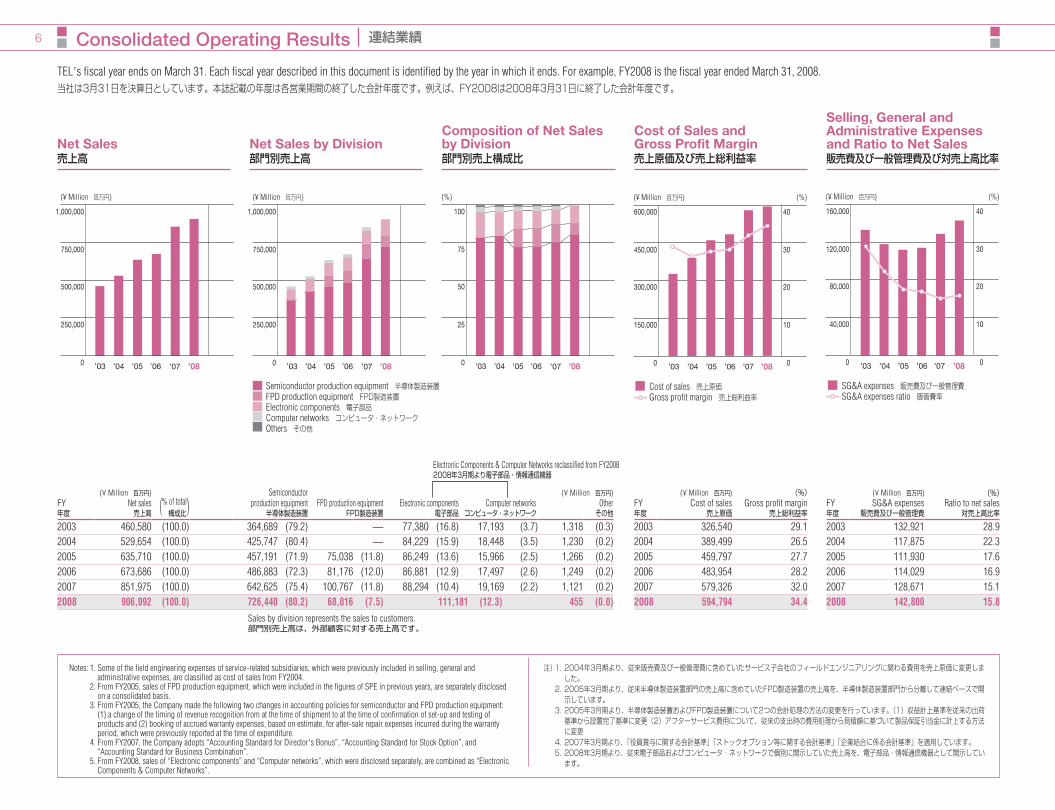
6 Consolidated Operating Results 連結業績
Net Sales売上高
1,000,000
750,000
500,000
250,000
0
(¥ Million 百万円)
’08’07’03 ’04 ’05 ’06
Net Sales by Division部門別売上高
1,000,000
750,000
500,000
250,000
0
(¥ Million 百万円)
Semiconductor production equipment 半導体製造装置FPD production equipment FPD製造装置Electronic components 電子部品Computer networks コンピュータ・ネットワークOthers その他
’08’07’03 ’04 ’05 ’06
Composition of Net Salesby Division部門別売上構成比
100
75
50
25
0
(%)
’08’07’03 ’04 ’05 ’06
TEL’s fiscal year ends on March 31. Each fiscal year described in this document is identified by the year in which it ends. For example, FY2008 is the fiscal year ended March 31, 2008.当社は3月31日を決算日としています。本誌記載の年度は各営業期間の終了した会計年度です。例えば、FY2008は2008年3月31日に終了した会計年度です。
Notes: 1. Some of the field engineering expenses of service-related subsidiaries, which were previously included in selling, general and administrative expenses, are classified as cost of sales from FY2004.
2. From FY2005, sales of FPD production equipment, which were included in the figures of SPE in previous years, are separately disclosed on a consolidated basis.
3. From FY2005, the Company made the following two changes in accounting policies for semiconductor and FPD production equipment: (1) a change of the timing of revenue recognition from at the time of shipment to at the time of confirmation of set-up and testing of products and (2) booking of accrued warranty expenses, based on estimate, for after-sale repair expenses incurred during the warranty period, which were previously reported at the time of expenditure.
4. From FY2007, the Company adopts “Accounting Standard for Director’s Bonus”, “Accounting Standard for Stock Option”, and “Accounting Standard for Business Combination”.
5. From FY2008, sales of “Electronic components” and “Computer networks”, which were disclosed separately, are combined as “Electronic Components & Computer Networks”.
注) 1. 2004年3月期より、従来販売費及び一般管理費に含めていたサービス子会社のフィールドエンジニアリングに関わる費用を売上原価に変更しました。
2. 2005年3月期より、従来半導体製造装置部門の売上高に含めていたFPD製造装置の売上高を、半導体製造装置部門から分離して連結ベースで開示しています。
3. 2005年3月期より、半導体製造装置およびFPD製造装置について2つの会計処理の方法の変更を行っています。(1)収益計上基準を従来の出荷基準から設置完了基準に変更(2)アフターサービス費用について、従来の支出時の費用処理から見積額に基づいて製品保証引当金に計上する方法に変更
4. 2007年3月期より、「役員賞与に関する会計基準」「ストックオプション等に関する会計基準」「企業結合に係る会計基準」を適用しています。 5. 2008年3月期より、従来電子部品およびコンピュータ・ネットワークで個別に開示していた売上高を、電子部品・情報通信機器として開示してい
ます。
Cost of Sales and Gross Profit Margin売上原価及び売上総利益率
600,000
450,000
300,000
150,000
0
40
30
20
10
0
(¥ Million 百万円) (%)
Cost of sales 売上原価Gross profit margin 売上総利益率
’08’03 ’04 ’05 ’06 ’07
Selling, General and Administrative Expenses and Ratio to Net Sales販売費及び一般管理費及び対売上高比率
160,000
120,000
80,000
40,000
0
40
30
20
10
0
(¥ Million 百万円) (%)
SG&A expenses 販売費及び一般管理費SG&A expenses ratio 販管費率
’08’03 ’04 ’05 ’06 ’07
FY年度
(¥ Million 百万円)Cost of sales
売上原価
(%)Gross profit margin
売上総利益率
2003 326,540 29.12004 389,499 26.52005 459,797 27.72006 483,954 28.22007 579,326 32.02008 594,794 34.4
FY年度
(¥ Million 百万円)Net sales
売上高 (% of total)構成比
Semiconductorproduction equipment
半導体製造装置FPD production equipment
FPD製造装置Electronic components
電子部品Computer networks
コンピュータ・ネットワーク
(¥ Million 百万円)Other
その他
2003 460,580 (100.0) 364,689 (79.2) — 77,380 (16.8) 17,193 (3.7) 1,318 (0.3)2004 529,654 (100.0) 425,747 (80.4) — 84,229 (15.9) 18,448 (3.5) 1,230 (0.2)2005 635,710 (100.0) 457,191 (71.9) 75,038 (11.8) 86,249 (13.6) 15,966 (2.5) 1,266 (0.2)2006 673,686 (100.0) 486,883 (72.3) 81,176 (12.0) 86,881 (12.9) 17,497 (2.6) 1,249 (0.2)2007 851,975 (100.0) 642,625 (75.4) 100,767 (11.8) 88,294 (10.4) 19,169 (2.2) 1,121 (0.2)2008 906,092 (100.0) 726,440 (80.2) 68,016 (7.5) 111,181 (12.3) 455 (0.0)
FY年度
(¥ Million 百万円)SG&A expenses
販売費及び一般管理費
(%)Ratio to net sales
対売上高比率
2003 132,921 28.92004 117,875 22.32005 111,930 17.62006 114,029 16.92007 128,671 15.12008 142,800 15.8
Electronic Components & Computer Networks reclassified from FY20082008年3月期より電子部品・情報通信機器
Sales by division represents the sales to customers.部門別売上高は、外部顧客に対する売上高です。
010_0454002472006.indd 6 2008/07/11 16:38:22
7
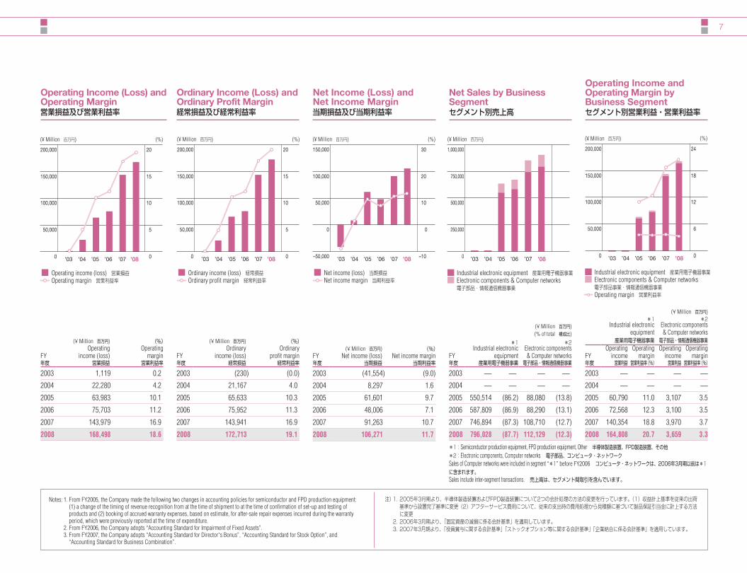
Operating Income and Operating Margin by Business Segmentセグメント別営業利益・営業利益率
Ordinary Income (Loss) and Ordinary Profit Margin経常損益及び経常利益率
200,000
150,000
100,000
50,000
0
24
(%)
18
12
6
0
(¥ Million 百万円)
’08’03 ’04 ’05 ’06 ’07
Industrial electronic equipment 産業用電子機器事業Electronic components & Computer networks 電子部品事業・情報通信機器事業Operating margin 営業利益率
Operating Income (Loss) and Operating Margin営業損益及び営業利益率
200,000
150,000
100,000
50,000
0
20
15
10
5
0
(¥ Million 百万円) (%)
Operating income (loss) 営業損益Operating margin 営業利益率
’08’03 ’04 ’05 ’06 ’07
200,000
150,000
100,000
50,000
0
20
15
10
5
0
(¥ Million 百万円) (%)
Ordinary income (loss) 経常損益Ordinary profit margin 経常利益率
’08’03 ’04 ’05 ’06 ’07
Net Income (Loss) andNet Income Margin当期損益及び当期利益率
150,000
100,000
50,000
0
–50,000
30
20
10
0
–10
(¥ Million 百万円) (%)
Net income (loss) 当期損益Net income margin 当期利益率
’08’03 ’04 ’05 ’06 ’07
Notes: 1. From FY2005, the Company made the following two changes in accounting policies for semiconductor and FPD production equipment: (1) a change of the timing of revenue recognition from at the time of shipment to at the time of confirmation of set-up and testing of products and (2) booking of accrued warranty expenses, based on estimate, for after-sale repair expenses incurred during the warranty period, which were previously reported at the time of expenditure.
2. From FY2006, the Company adopts “Accounting Standard for Impairment of Fixed Assets”. 3. From FY2007, the Company adopts “Accounting Standard for Director’s Bonus”, “Accounting Standard for Stock Option”, and
“Accounting Standard for Business Combination”.
注) 1. 2005年3月期より、半導体製造装置およびFPD製造装置について2つの会計処理の方法の変更を行っています。(1)収益計上基準を従来の出荷基準から設置完了基準に変更(2)アフターサービス費用について、従来の支出時の費用処理から見積額に基づいて製品保証引当金に計上する方法に変更
2. 2006年3月期より、「固定資産の減損に係る会計基準」を適用しています。 3. 2007年3月期より、「役員賞与に関する会計基準」「ストックオプション等に関する会計基準」「企業結合に係る会計基準」を適用しています。
Net Sales by Business Segmentセグメント別売上高
*1Industrial electronic
equipment産業用電子機器事業
(¥ Million 百万円)*2
Electronic components& Computer networks
電子部品・情報通信機器事業
FY年度
Operatingincome
営業利益
Operatingmargin
営業利益率(%)
Operatingincome
営業利益
Operatingmargin
営業利益率(%)
2003 — — — —2004 — — — —2005 60,790 11.0 3,107 3.5
2006 72,568 12.3 3,100 3.5
2007 140,354 18.8 3,970 3.7
2008 164,808 20.7 3,659 3.3
FY年度
(¥ Million 百万円)Ordinary
income (loss)経常損益
(%)Ordinary
profit margin経常利益率
2003 (230) (0.0)
2004 21,167 4.0
2005 65,633 10.3
2006 75,952 11.3
2007 143,941 16.9
2008 172,713 19.1
FY年度
(¥ Million 百万円)Operating
income (loss)営業損益
(%)Operating
margin営業利益率
2003 1,119 0.2
2004 22,280 4.2
2005 63,983 10.1
2006 75,703 11.2
2007 143,979 16.9
2008 168,498 18.6
FY年度
(¥ Million 百万円)Net income (loss)
当期損益
(%)Net income margin
当期利益率
2003 (41,554) (9.0)
2004 8,297 1.6
2005 61,601 9.7
2006 48,006 7.1
2007 91,263 10.7
2008 106,271 11.7
FY年度
*1Industrial electronic
equipment産業用電子機器事業
(¥ Million 百万円)(% of total 構成比)
*2Electronic components& Computer networks
電子部品・情報通信機器事業
2003 — — — —2004 — — — —2005 550,514 (86.2) 88,080 (13.8)
2006 587,809 (86.9) 88,290 (13.1)
2007 746,894 (87.3) 108,710 (12.7)
2008 796,028 (87.7) 112,129 (12.3)
1,000,000
750,000
500,000
250,000
0
(¥ Million 百万円)
’08’03 ’04 ’05 ’06 ’07
Industrial electronic equipment 産業用電子機器事業Electronic components & Computer networks 電子部品・情報通信機器事業
*1:Semiconductor production equipment, FPD production equipment, Other 半導体製造装置、FPD製造装置、その他*2:Electronic components, Computer networks 電子部品、コンピュータ・ネットワークSales of Computer networks were included in segment “*1” before FY2006 コンピュータ・ネットワークは、2006年3月期以前は*1に含まれます。Sales include inter-segment transactions. 売上高は、セグメント間取引を含んでいます。
010_0454002472006.indd 7 2008/07/11 16:38:23
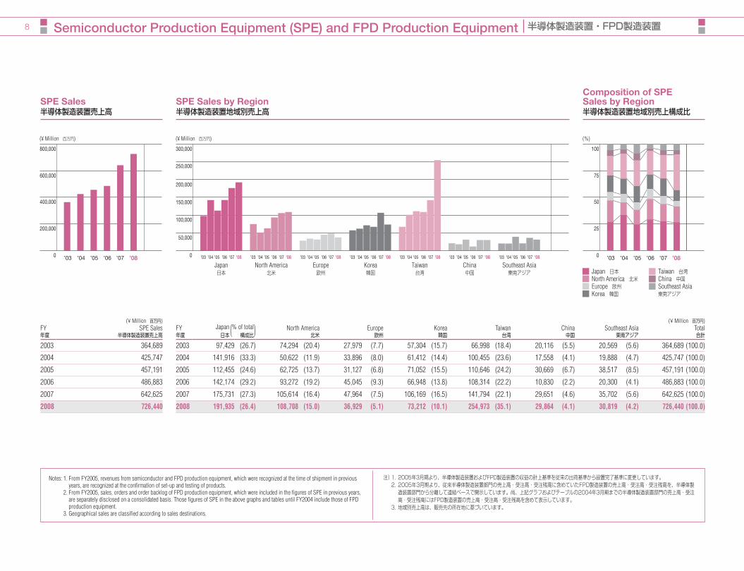
8 Semiconductor Production Equipment (SPE) and FPD Production Equipment 半導体製造装置・FPD製造装置
SPE Sales半導体製造装置売上高
SPE Sales by Region半導体製造装置地域別売上高
Composition of SPE Sales by Region半導体製造装置地域別売上構成比
FY年度
(¥ Million 百万円)SPE Sales
半導体製造装置売上高
2003 364,689
2004 425,747
2005 457,191
2006 486,883
2007 642,625
2008 726,440
FY年度
Japan (% of total)日本 構成比North America
北米Europe
欧州Korea
韓国Taiwan
台湾China
中国Southeast Asia
東南アジア
(¥ Million 百万円)Total合計
2003 97,429 (26.7) 74,294 (20.4) 27,979 (7.7) 57,304 (15.7) 66,998 (18.4) 20,116 (5.5) 20,569 (5.6) 364,689 (100.0)
2004 141,916 (33.3) 50,622 (11.9) 33,896 (8.0) 61,412 (14.4) 100,455 (23.6) 17,558 (4.1) 19,888 (4.7) 425,747 (100.0)
2005 112,455 (24.6) 62,725 (13.7) 31,127 (6.8) 71,052 (15.5) 110,646 (24.2) 30,669 (6.7) 38,517 (8.5) 457,191 (100.0)
2006 142,174 (29.2) 93,272 (19.2) 45,045 (9.3) 66,948 (13.8) 108,314 (22.2) 10,830 (2.2) 20,300 (4.1) 486,883 (100.0)
2007 175,731 (27.3) 105,614 (16.4) 47,964 (7.5) 106,169 (16.5) 141,794 (22.1) 29,651 (4.6) 35,702 (5.6) 642,625 (100.0)
2008 191,935 (26.4) 108,708 (15.0) 36,929 (5.1) 73,212 (10.1) 254,973 (35.1) 29,864 (4.1) 30,819 (4.2) 726,440 (100.0)
800,000
600,000
400,000
200,000
0
(¥ Million 百万円)
’08’03 ’04 ’05 ’06 ’07
300,000
250,000
150,000
200,000
100,000
50,000
0
(¥ Million 百万円)
’08’03 ’04 ’05 ’06 ’07 ’08’03 ’04 ’05 ’06 ’07 ’08’03 ’04 ’05 ’06 ’07 ’08’03 ’04 ’05 ’06 ’07 ’08’03 ’04 ’05 ’06 ’07 ’08’03 ’04 ’05 ’06 ’07 ’08’03 ’04 ’05 ’06 ’07
Japan日本
North America北米
Europe欧州
Korea韓国
Taiwan台湾
China中国
Southeast Asia東南アジア
100
75
50
25
0
(%)
Japan 日本North America 北米Europe 欧州Korea 韓国
Taiwan 台湾China 中国Southeast Asia 東南アジア
’08’03 ’04 ’05 ’06 ’07
Notes: 1. From FY2005, revenues from semiconductor and FPD production equipment, which were recognized at the time of shipment in previous years, are recognized at the confirmation of set-up and testing of products.
2. From FY2005, sales, orders and order backlog of FPD production equipment, which were included in the figures of SPE in previous years, are separately disclosed on a consolidated basis. Those figures of SPE in the above graphs and tables until FY2004 include those of FPD production equipment.
3. Geographical sales are classified according to sales destinations.
注) 1. 2005年3月期より、半導体製造装置およびFPD製造装置の収益の計上基準を従来の出荷基準から設置完了基準に変更しています。 2. 2005年3月期より、従来半導体製造装置部門の売上高・受注高・受注残高に含めていたFPD製造装置の売上高・受注高・受注残高を、半導体製
造装置部門から分離して連結ベースで開示しています。尚、上記グラフおよびテーブルの2004年3月期までの半導体製造装置部門の売上高・受注高・受注残高にはFPD製造装置の売上高・受注高・受注残高を含めて表示しています。
3. 地域別売上高は、販売先の所在地に基づいています。
010_0454002472006.indd 8 2008/07/11 16:38:24
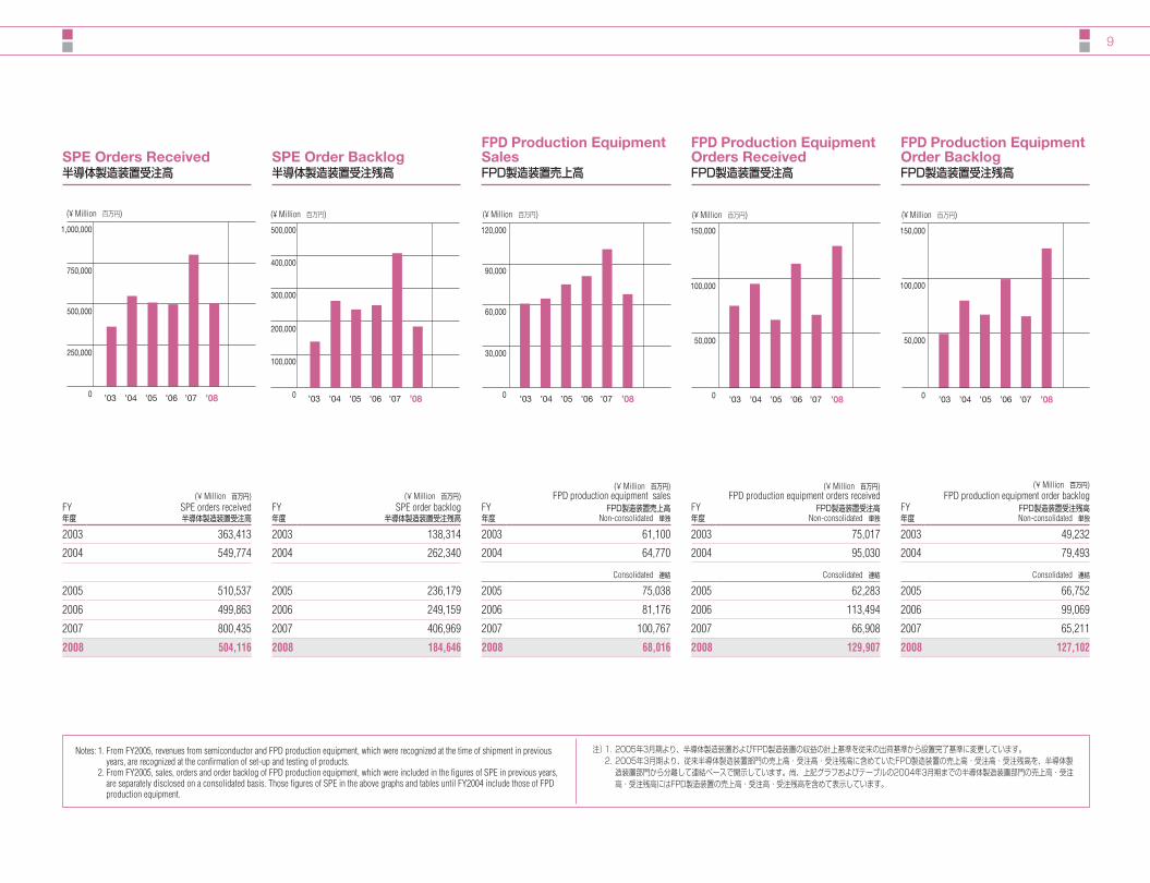
9
SPE Orders Received半導体製造装置受注高
SPE Order Backlog半導体製造装置受注残高
FPD Production Equipment Orders ReceivedFPD製造装置受注高
FPD Production Equipment Order BacklogFPD製造装置受注残高
FY年度
(¥ Million 百万円)SPE orders received半導体製造装置受注高
2003 363,413
2004 549,774
2005 510,537
2006 499,863
2007 800,435
2008 504,116
FY年度
(¥ Million 百万円)FPD production equipment orders received
FPD製造装置受注高Non-consolidated 単独
2003 75,017
2004 95,030
Consolidated 連結
2005 62,283
2006 113,494
2007 66,908
2008 129,907
FY年度
(¥ Million 百万円)FPD production equipment order backlog
FPD製造装置受注残高Non-consolidated 単独
2003 49,232
2004 79,493
Consolidated 連結
2005 66,752
2006 99,069
2007 65,211
2008 127,102
1,000,000
750,000
500,000
250,000
0
(¥ Million 百万円)
’08’03 ’04 ’05 ’06 ’07
500,000
300,000
400,000
200,000
100,000
0
(¥ Million 百万円)
’08’03 ’04 ’05 ’06 ’07
150,000
100,000
50,000
0
(¥ Million 百万円)
’08’03 ’04 ’05 ’06 ’07
FPD Production Equipment SalesFPD製造装置売上高
FY年度
(¥ Million 百万円)FPD production equipment sales
FPD製造装置売上高Non-consolidated 単独
2003 61,100
2004 64,770
Consolidated 連結
2005 75,038
2006 81,176
2007 100,767
2008 68,016
120,000
90,000
60,000
30,000
0
(¥ Million 百万円)
’08’03 ’04 ’05 ’06 ’07
150,000
100,000
50,000
0
(¥ Million 百万円)
’08’03 ’04 ’05 ’06 ’07
FY年度
(¥ Million 百万円)SPE order backlog
半導体製造装置受注残高
2003 138,314
2004 262,340
2005 236,179
2006 249,159
2007 406,969
2008 184,646
Notes: 1. From FY2005, revenues from semiconductor and FPD production equipment, which were recognized at the time of shipment in previous years, are recognized at the confirmation of set-up and testing of products.
2. From FY2005, sales, orders and order backlog of FPD production equipment, which were included in the figures of SPE in previous years, are separately disclosed on a consolidated basis. Those figures of SPE in the above graphs and tables until FY2004 include those of FPD production equipment.
注) 1. 2005年3月期より、半導体製造装置およびFPD製造装置の収益の計上基準を従来の出荷基準から設置完了基準に変更しています。 2. 2005年3月期より、従来半導体製造装置部門の売上高・受注高・受注残高に含めていたFPD製造装置の売上高・受注高・受注残高を、半導体製
造装置部門から分離して連結ベースで開示しています。尚、上記グラフおよびテーブルの2004年3月期までの半導体製造装置部門の売上高・受注高・受注残高にはFPD製造装置の売上高・受注高・受注残高を含めて表示しています。
010_0454002472006.indd 9 2008/07/11 16:38:25
10 Consolidated Financial Data 連結財務データ
Working Capital and Current Ratio運転資本及び流動比率
FY年度
(¥ Million 百万円)Working capital
運転資本
(%)Current ratio
流動比率
2003 195,733 221.8
2004 261,502 284.8
2005 288,575 239.7
2006 315,861 256.7
2007 384,508 270.2
2008 441,413 322.0
500,000
400,000
200,000
100,000
0
400
320
160
300,000 240
80
0
(¥ Million 百万円) (%)
Working capital 運転資本Current ratio 流動比率
’08’03 ’04 ’05 ’06 ’07
Working capital = Current assets – Current liabilities運転資本=流動資産−流動負債Current ratio = Current assets / Current liabilities × 100流動比率=流動資産÷流動負債×100(%)
Receivable Turnover 売上債権回転日数
FY年度
(Days 日)Receivable turnover
売上債権回転日数
2003 135
2004 159
2005 99
2006 92
2007 98
2008 90
Receivable turnover = Trade notes and accounts receivable at fiscal year-end / Net sales × 365
売上債権回転日数=期末受取手形及び売掛金÷売上高×365
200
150
100
50
0
(Days 日)
’08’03 ’04 ’05 ’06 ’07
Inventory Turnoverたな卸資産回転日数
FY年度
(Days 日)Inventory turnoverたな卸資産回転日数
2003 89
2004 72
2005 93
2006 89
2007 83
2008 65
Inventory turnover = Inventories at fiscal year-end / Net sales × 365
たな卸資産回転日数=期末たな卸資産÷売上高×365
200
150
100
50
0
(Days 日)
’08’03 ’04 ’05 ’06 ’07
Interest-Bearing Debt andDebt-to-Equity Ratio有利子負債及びデット・エクイティ・レシオ
FY年度
(¥ Million 百万円)Interest-bearing
debt有利子負債
(%)Debt-to-equity ratioデット・エクイティ・
レシオ
2003 151,362 59.8
2004 127,045 46.1
2005 99,451 29.9
2006 65,100 17.3
2007 40,212 8.7
2008 36,070 6.7
Debt-to-equity ratio = Interest-bearing debt / Total equity at fiscal year-end
デット・エクイティ・レシオ=有利子負債÷期末自己資本×100(%)
200,000
150,000
100,000
50,000
0
80
60
40
20
0
(¥ Million 百万円) (%)
Interest-bearing debt 有利子負債Debt-to-equity ratio デット・エクイティ・レシオ
’08’03 ’04 ’05 ’06 ’07
Equity and Equity Ratio自己資本及び自己資本比率
FY年度
(¥ Million 百万円)Equity
自己資本
(%)Equity ratio自己資本比率
2003 252,904 48.2
2004 275,800 49.1
2005 332,165 51.6
2006 376,900 56.8
2007 460,175 59.7
2008 534,954 67.5
600,000
450,000
300,000
150,000
0
80
60
40
20
0
(¥ Million 百万円) (%)
Equity 自己資本Equity ratio 自己資本比率
’08’03 ’04 ’05 ’06 ’07
Notes: 1. From FY2005, the Company made the following two changes in accounting policies for semiconductor and FPD production equipment: (1) a change of the timing of revenue recognition from at the time of shipment to at the time of confirmation of set-up and testing of products and (2) booking of accrued warranty expenses, based on estimate, for after-sale repair expenses incurred during the warranty period, which were previously reported at the time of expenditure.
2. The figure for trade notes and accounts receivable used for calculation of the receivable turnover does not include the figure for non-trade accounts receivable.
3. From FY2007, the Company adopts “Accounting Standard for Presentation of Net Assets in the Balance Sheets”, “Accounting Standard for Director’s Bonus”, “Accounting Standard for Stock Option”, and “Accounting Standard for Business Combination”
注) 1. 2005年3月期より、半導体製造装置およびFPD製造装置について2つの会計処理の方法の変更を行っています。(1)収益計上基準を従来の出荷基準から設置完了基準に変更(2)アフターサービス費用について、従来の支出時の費用処理から見積額に基づいて製品保証引当金に計上する方法に変更
2. 売上債権回転日数の計算の元になる「受取手形及び売掛金」の数字には未収金を含んでいません。 3. 2007年3月期より「貸借対照表の純資産の部の表示に関する会計基準」「役員賞与に関する会計基準」「ストックオプション等に関する会計基準」
「企業結合に係る会計基準」を適用しています。
From FY2007, Equity = Net assets – subscription rights to shares – Minority interests
2007年3月期より、自己資本=純資産−新株予約権−少数株主持分
010_0454002472006.indd 10 2008/07/11 16:38:26
11
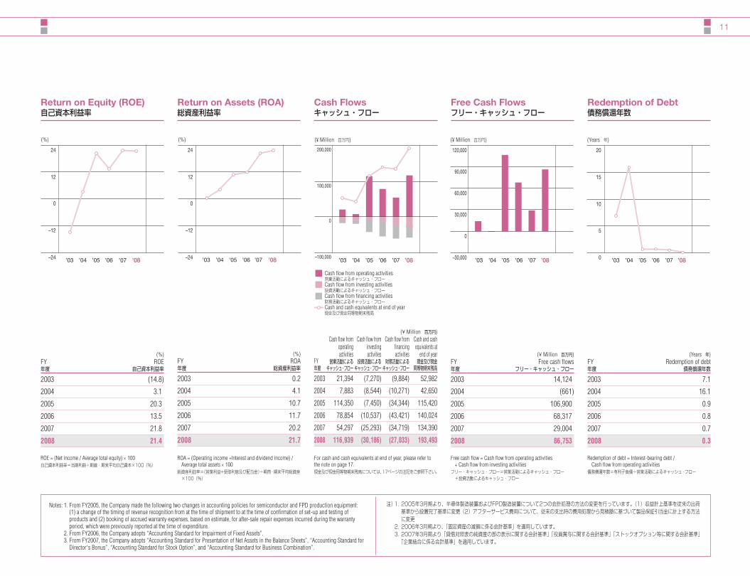
Cash Flowsキャッシュ・フロー
Free Cash Flowsフリー・キャッシュ・フロー
(¥ Million 百万円)
FY年度
Cash flow fromoperatingactivities
営業活動によるキャッシュ・フロー
Cash flow frominvestingactivities
投資活動によるキャッシュ・フロー
Cash flow fromfinancingactivities
財務活動によるキャッシュ・フロー
Cash and cashequivalents at
end of year現金及び現金
同等物期末残高
2003 21,394 (7,270) (9,884) 52,982
2004 7,883 (8,544) (10,271) 42,650
2005 114,350 (7,450) (34,344) 115,420
2006 78,854 (10,537) (43,421) 140,024
2007 54,297 (25,293) (34,719) 134,390
2008 116,939 (30,186) (27,033) 193,493
FY年度
(¥ Million 百万円)Free cash flows
フリー・キャッシュ・フロー
2003 14,124
2004 (661)
2005 106,900
2006 68,317
2007 29,004
2008 86,753
Free cash flow = Cash flow from operating activities + Cash flow from investing activities
フリー・キャッシュ・フロー=営業活動によるキャッシュ・フロー +投資活動によるキャッシュ・フロー
200,000
100,000
0
–100,000
(¥ Million 百万円)
Cash flow from operating activities 営業活動によるキャッシュ・フローCash flow from investing activities 投資活動によるキャッシュ・フローCash flow from financing activities 財務活動によるキャッシュ・フローCash and cash equivalents at end of year 現金及び現金同等物期末残高
’08’03 ’04 ’05 ’06 ’07
120,000
90,000
60,000
30,000
0
–30,000
(¥ Million 百万円)
’08’03 ’04 ’05 ’06 ’07
Redemption of Debt債務償還年数
FY年度
(Years 年)Redemption of debt
債務償還年数
2003 7.1
2004 16.1
2005 0.9
2006 0.8
2007 0.7
2008 0.3
Redemption of debt = Interest-bearing debt / Cash flow from operating activities
債務償還年数=有利子負債÷営業活動によるキャッシュ・フロー
20
0
(Years 年)
5
10
15
’08’03 ’04 ’05 ’06 ’07
Return on Equity (ROE)自己資本利益率
FY年度
(%)ROE
自己資本利益率
2003 (14.8)
2004 3.1
2005 20.3
2006 13.5
2007 21.8
2008 21.4
ROE = (Net income / Average total equity) × 100自己資本利益率=当期利益÷期首・期末平均自己資本×100(%)
24
12
0
–12
–24
(%)
’08’07’03 ’04 ’05 ’06
Return on Assets (ROA)総資産利益率
FY年度
(%)ROA
総資産利益率
2003 0.2
2004 4.1
2005 10.7
2006 11.7
2007 20.2
2008 21.7
ROA = (Operating income +Interest and dividend income) / Average total assets × 100
総資産利益率=(営業利益+受取利息及び配当金)÷期首・期末平均総資産 ×100(%)
For cash and cash equivalents at end of year, please refer to the note on page 17.現金及び現金同等物期末残高については、17ページの注記をご参照下さい。
’08’03 ’04 ’05 ’06 ’07
24
12
0
–12
–24
(%)
Notes: 1. From FY2005, the Company made the following two changes in accounting policies for semiconductor and FPD production equipment: (1) a change of the timing of revenue recognition from at the time of shipment to at the time of confirmation of set-up and testing of products and (2) booking of accrued warranty expenses, based on estimate, for after-sale repair expenses incurred during the warranty period, which were previously reported at the time of expenditure.
2. From FY2006, the Company adopts “Accounting Standard for Impairment of Fixed Assets”. 3. From FY2007, the Company adopts “Accounting Standard for Presentation of Net Assets in the Balance Sheets”, “Accounting Standard for
Director’s Bonus”, “Accounting Standard for Stock Option”, and “Accounting Standard for Business Combination”.
注) 1. 2005年3月期より、半導体製造装置およびFPD製造装置について2つの会計処理の方法の変更を行っています。(1)収益計上基準を従来の出荷基準から設置完了基準に変更(2)アフターサービス費用について、従来の支出時の費用処理から見積額に基づいて製品保証引当金に計上する方法に変更
2. 2006年3月期より、「固定資産の減損に係る会計基準」を適用しています。 3. 2007年3月期より「貸借対照表の純資産の部の表示に関する会計基準」「役員賞与に関する会計基準」「ストックオプション等に関する会計基準」
「企業結合に係る会計基準」を適用しています。
010_0454002472006.indd 11 2008/07/11 16:38:27

12
Interest Coverage Ratioインタレスト・カバレッジ・レシオ
FY年度
(Times 倍)Interest coverage ratio
インタレスト・カバレッジ・レシオ
2003 0.8
2004 16.9
2005 58.7
2006 111.0
2007 344.4
2008 494.9
Interest coverage ratio = (Operating income + Interest and dividend income) / Interest expenses
インタレスト・カバレッジ・レシオ=(営業利益 +受取利息及び配当金)÷支払利息(倍)
500
400
300
200
100
0
–100
(Times 倍)
’08’03 ’04 ’05 ’06 ’07
R&D Expenses研究開発費
Capital Expenditures andDepreciation Expenses設備投資額及び減価償却実施額
FY年度
(¥ Million 百万円)R&D expenses
研究開発費
2003 50,123
2004 44,150
2005 43,889
2006 49,182
2007 56,962
2008 66,073
FY年度
Capitalexpenditures
設備投資額
(¥ Million 百万円)Depreciation
expenses減価償却実施額
2003 12,359 27,374
2004 11,007 24,963
2005 9,876 21,463
2006 13,335 19,170
2007 27,129 18,820
2008 22,703 21,413
80,000
60,000
40,000
20,000
0
(¥ Million 百万円)
’08’03 ’04 ’05 ’06 ’07
’08’07
40,000
30,000
20,000
10,000
0
(¥ Million 百万円)
Capital expenditures 設備投資額Depreciation expenses 減価償却実施額
’08’03 ’04 ’05 ’06 ’07
Number of Employees Worldwide従業員数
FY年度
(People 人)Number of employees worldwide
従業員数
2003 10,053
2004 8,870
2005 8,864
2006 8,901
2007 9,528
2008 10,429
12,000
9,000
6,000
3,000
0
(Persons 人)
’08’03 ’04 ’05 ’06 ’07
Net Income (Loss) perEmployee1人当り当期利益(損失)
15
10
5
0
–5
(¥ Million 百万円)
’08’03 ’04 ’05 ’06 ’07
FY年度
(¥ Million 百万円)Net income (loss) per employee
1人当り当期利益(損失)
2003 (4.1)
2004 0.9
2005 6.9
2006 5.4
2007 9.6
2008 10.2
Notes: 1. Amortization of goodwill is not included in depreciation expenses. 2. From FY2007, the Company adopts “Accounting Standard for Director’s Bonus”, “Accounting Standard for Stock Option”, and
“Accounting Standard for Business Combination”
注) 1. 減価償却実施額には、のれん償却額は含まれておりません 2. 2007年3月期より、「役員賞与に関する会計基準」「ストックオプション等に関する会計基準」「企業結合に係る会計基準」を適用しています。
010_0454002472006.indd 12 2008/07/11 16:38:28

13
Net Income (Loss) per Share1株当り当期利益(損失)
Cash Flow per Share1株当りキャッシュ・フロー
Net Assets per Share1株当り純資産
Cash Dividends per Share1株当り配当金
Payout Ratio配当性向
FY年度
(¥ 円)Net income (loss) per share
1株当り当期利益(損失)
2003 (238.57)
2004 46.37
2005 343.63
2006 267.61
2007 511.27
2008 594.01
Net income (loss) per share = Net income (loss) / Average total number of shares outstanding in each fiscal year
1株当り当期利益(損失)=当期利益(損失) ÷期中平均発行済株式総数
FY年度
(¥ 円)Cash flow per share
1株当りキャッシュ・フロー
2003 (81.39)
2004 188.31
2005 465.99
2006 377.08
2007 616.71
2008 713.70
Cash flow per share = (Net income + Depreciation and amortization) / Average total number of shares outstanding in each fiscal year
1株当りキャッシュ・フロー=(当期利益+減価償却費) ÷期中平均発行済株式総数
FY年度
(¥ 円)Net assets per share
1株当り純資産
2003 1,456.23
2004 1,543.73
2005 1,863.28
2006 2,112.30
2007 2,573.72
2008 2,989.70
Net assets per share = Net assets / Total number of shares issued
1株当り純資産=期末純資産÷期末発行済株式総数
FY年度
(¥ 円)Cash dividends per share
1株当り配当金
2003 8.00
2004 10.00
2005 45.00
2006 55.00
2007 103.00
2008 125.00
FY年度
(%)Payout ratio
配当性向Non-consolidated 単独
2003 —
2004 47.4
2005 23.9
Consolidated 連結
2006 20.6
2007 20.1
2008 21.0
Payout ratio = Cash dividends per share / Non-consolidated Net income per share × 100
配当性向=1株当り配当金額÷単独1株当り当期純利益×100(%)
900
600
300
0
–300
(¥ 円)
’08’03 ’04 ’05 ’06 ’07
800
400
600
200
0
–200
(¥ 円)
’08’03 ’04 ’05 ’06 ’07
3,000
2,250
1,500
750
0
(¥ 円)
’08’03 ’04 ’05 ’06 ’07
125
100
75
25
50
0
(¥ 円)
’08’03 ’04 ’05 ’06 ’07
60
45
30
15
0
(%)
’08’03 ’04 ’05 ’06 ’07
Notes: 1. The payout ratios of FY2003 are not indicated due to net loss on a non-consolidated basis. 2. From FY2005, the Company made the following two changes in accounting policies for semiconductor and FPD production equipment:
(1) a change of the timing of revenue recognition from at the time of shipment to at the time of confirmation of set-up and testing of products and (2) booking of accrued warranty expenses, based on estimate, for after-sale repair expenses incurred during the warranty period, which were previously reported at the time of expenditure.
3. From FY2006, the Company adopts “Accounting Standard for Impairment of Fixed Assets”. 4. From FY2007, the Company adopts “Accounting Standard for Presentation of Net Assets in the Balance Sheets”, “Accounting Standard for
Director’s Bonus”, “Accounting Standard for Stock Option”, and “Accounting Standard for Business Combination” 5. The number of shares outstanding excluding the treasury stock is used for calculation of per share data.
注) 1. 2003年3月期の配当性向は、単独ベースで当期純損失を計上したため掲載しておりません。 2. 2005年3月期より、半導体製造装置およびFPD製造装置について2つの会計処理の方法の変更を行っています。(1)収益計上基準を従来の出荷
基準から設置完了基準に変更(2)アフターサービス費用について、従来の支出時の費用処理から見積額に基づいて製品保証引当金に計上する方法に変更
3. 2006年3月期より、「固定資産の減損に係る会計基準」を適用しています。 4. 2007年3月期より「貸借対照表の純資産の部の表示に関する会計基準」「役員賞与に関する会計基準」「ストックオプション等に関する会計基準」
「企業結合に係る会計基準」を適用しています。 5. 1株当り指標の計算には自己株式数を控除後の発行済株式数を使用しています。
010_0454002472006.indd 13 2008/07/11 16:38:29
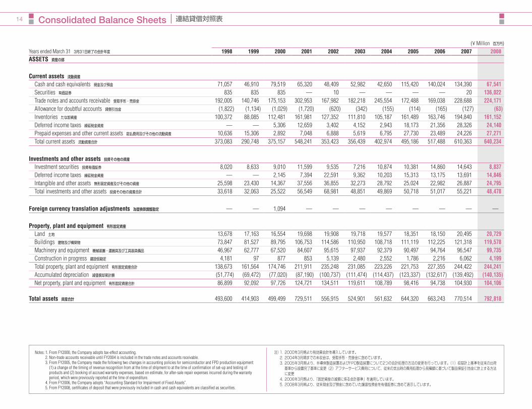
14 Consolidated Balance Sheets 連結貸借対照表
(¥ Million 百万円)Years ended March 31 3月31日終了の会計年度 1998 1999 2000 2001 2002 2003 2004 2005 2006 2007 2008ASSETS 資産の部
Current assets 流動資産
Cash and cash equivalents 現金及び預金 71,057 46,910 79,519 65,320 48,409 52,982 42,650 115,420 140,024 134,390 67,541Securities 有価証券 835 835 835 — 10 — — — — 20 136,022Trade notes and accounts receivable 受取手形・売掛金 192,005 140,746 175,153 302,953 167,982 182,218 245,554 172,488 169,038 228,688 224,171Allowance for doubtful accounts 貸倒引当金 (1,822) (1,134) (1,029) (1,720) (620) (342) (155) (114) (165) (127) (63)Inventories たな卸資産 100,372 88,085 112,481 161,981 127,352 111,810 105,187 161,489 163,746 194,840 161,152Deferred income taxes 繰延税金資産 — — 5,306 12,659 3,402 4,152 2,943 18,173 21,356 28,326 24,140Prepaid expenses and other current assets 前払費用及びその他の流動資産 10,636 15,306 2,892 7,048 6,888 5,619 6,795 27,730 23,489 24,226 27,271Total current assets 流動資産合計 373,083 290,748 375,157 548,241 353,423 356,439 402,974 495,186 517,488 610,363 640,234
Investments and other assets 投資その他の資産
Investment securities 投資有価証券 8,020 8,633 9,010 11,599 9,535 7,216 10,874 10,381 14,860 14,643 8,837Deferred income taxes 繰延税金資産 — — 2,145 7,394 22,591 9,362 10,203 15,313 13,175 13,691 14,846Intangible and other assets 無形固定資産及びその他の資産 25,598 23,430 14,367 37,556 36,855 32,273 28,792 25,024 22,982 26,887 24,795Total investments and other assets 投資その他の資産合計 33,618 32,063 25,522 56,549 68,981 48,851 49,869 50,718 51,017 55,221 48,478
Foreign currency translation adjustments 為替換算調整勘定 — — 1,094 — — — — — — — —
Property, plant and equipment 有形固定資産
Land 土地 13,678 17,163 16,554 19,698 19,908 19,718 19,577 18,351 18,150 20,495 20,729Buildings 建物及び構築物 73,847 81,527 89,795 106,753 114,586 110,950 108,718 111,119 112,225 121,318 119,578Machinery and equipment 機械装置・運搬具及び工具器具備品 46,967 62,777 67,520 84,607 95,615 97,937 92,379 90,497 94,764 96,547 99,735Construction in progress 建設仮勘定 4,181 97 877 853 5,139 2,480 2,552 1,786 2,216 6,062 4,199Total property, plant and equipment 有形固定資産合計 138,673 161,564 174,746 211,911 235,248 231,085 223,226 221,753 227,355 244,422 244,241Accumulated depreciation 減価償却累計額 (51,774) (69,472) (77,020) (87,190) (100,737) (111,474) (114,437) (123,337) (132,617) (139,492) (140,135)Net property, plant and equipment 有形固定資産合計 86,899 92,092 97,726 124,721 134,511 119,611 108,789 98,416 94,738 104,930 104,106
Total assets 資産合計 493,600 414,903 499,499 729,511 556,915 524,901 561,632 644,320 663,243 770,514 792,818
Notes: 1. From FY2000, the Company adopts tax-effect accounting. 2. Non-trade accounts receivable until FY2004 is included in the trade notes and accounts receivable. 3. From FY2005, the Company made the following two changes in accounting policies for semiconductor and FPD production equipment:
(1) a change of the timing of revenue recognition from at the time of shipment to at the time of confirmation of set-up and testing of products and (2) booking of accrued warranty expenses, based on estimate, for after-sale repair expenses incurred during the warranty period, which were previously reported at the time of expenditure.
4. From FY2006, the Company adopts “Accounting Standard for Impairment of Fixed Assets”. 5. From FY2008, certificates of deposit that were previously included in cash and cash equivalents are classified as securities.
注) 1. 2000年3月期より税効果会計を導入しています。 2. 2004年3月期までの未収金は、受取手形・売掛金に含めています。 3. 2005年3月期より、半導体製造装置およびFPD製造装置について2つの会計処理の方法の変更を行っています。(1)収益計上基準を従来の出荷
基準から設置完了基準に変更(2)アフターサービス費用について、従来の支出時の費用処理から見積額に基づいて製品保証引当金に計上する方法に変更
4. 2006年3月期より、「固定資産の減損に係る会計基準」を適用しています。 5. 2008年3月期より、従来現金及び預金に含めていた譲渡性預金を有価証券に含めて表示しています。
010_0454002472006.indd 14 2008/07/11 16:38:29
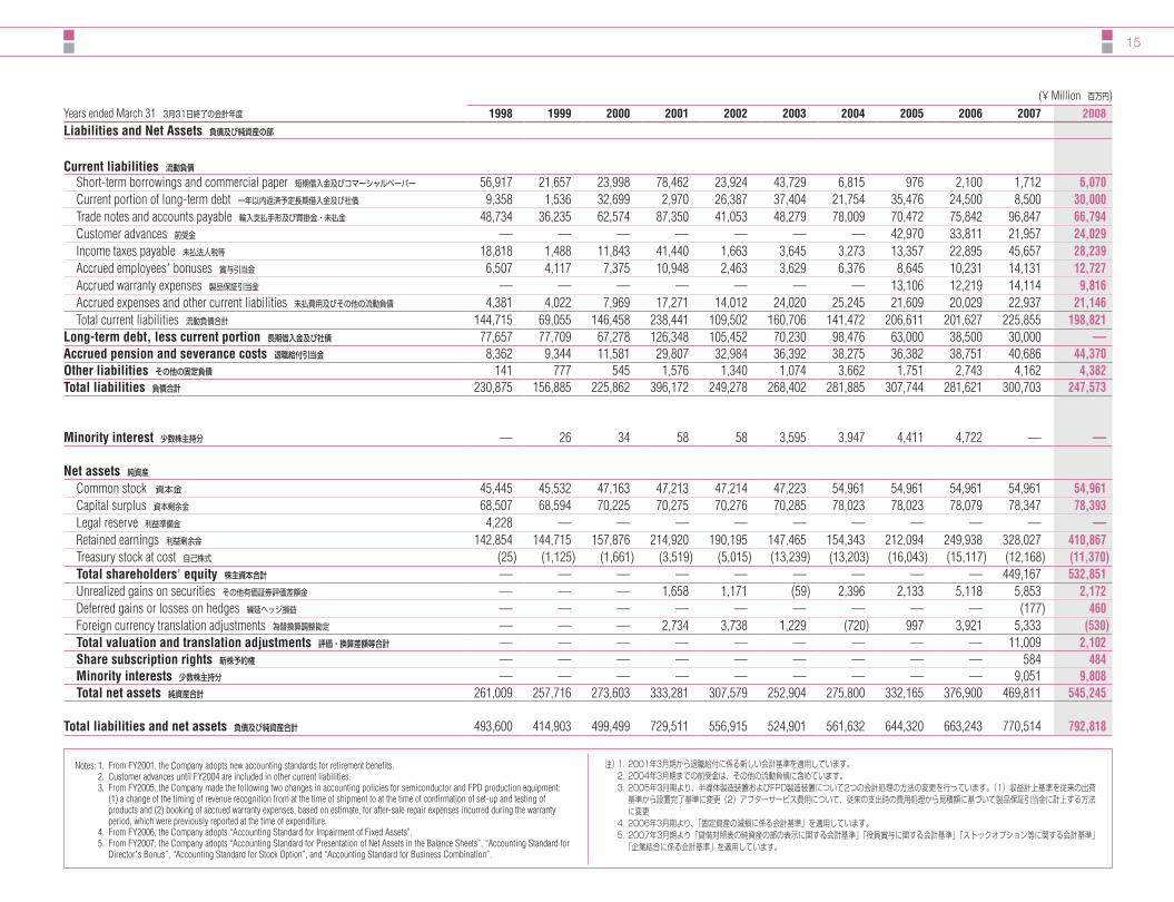
15
(¥ Million 百万円)Years ended March 31 3月31日終了の会計年度 1998 1999 2000 2001 2002 2003 2004 2005 2006 2007 2008Liabilities and Net Assets 負債及び純資産の部
Current liabilities 流動負債
Short-term borrowings and commercial paper 短期借入金及びコマーシャルペーパー 56,917 21,657 23,998 78,462 23,924 43,729 6,815 976 2,100 1,712 6,070Current portion of long-term debt 一年以内返済予定長期借入金及び社債 9,358 1,536 32,699 2,970 26,387 37,404 21,754 35,476 24,500 8,500 30,000Trade notes and accounts payable 輸入支払手形及び買掛金・未払金 48,734 36,235 62,574 87,350 41,053 48,279 78,009 70,472 75,842 96,847 66,794Customer advances 前受金 — — — — — — — 42,970 33,811 21,957 24,029Income taxes payable 未払法人税等 18,818 1,488 11,843 41,440 1,663 3,645 3,273 13,357 22,895 45,657 28,239Accrued employees’ bonuses 賞与引当金 6,507 4,117 7,375 10,948 2,463 3,629 6,376 8,645 10,231 14,131 12,727Accrued warranty expenses 製品保証引当金 — — — — — — — 13,106 12,219 14,114 9,816Accrued expenses and other current liabilities 未払費用及びその他の流動負債 4,381 4,022 7,969 17,271 14,012 24,020 25,245 21,609 20,029 22,937 21,146Total current liabilities 流動負債合計 144,715 69,055 146,458 238,441 109,502 160,706 141,472 206,611 201,627 225,855 198,821
Long-term debt, less current portion 長期借入金及び社債 77,657 77,709 67,278 126,348 105,452 70,230 98,476 63,000 38,500 30,000 —Accrued pension and severance costs 退職給付引当金 8,362 9,344 11,581 29,807 32,984 36,392 38,275 36,382 38,751 40,686 44,370Other liabilities その他の固定負債 141 777 545 1,576 1,340 1,074 3,662 1,751 2,743 4,162 4,382Total liabilities 負債合計 230,875 156,885 225,862 396,172 249,278 268,402 281,885 307,744 281,621 300,703 247,573
Minority interest 少数株主持分 — 26 34 58 58 3,595 3,947 4,411 4,722 — —
Net assets 純資産
Common stock 資本金 45,445 45,532 47,163 47,213 47,214 47,223 54,961 54,961 54,961 54,961 54,961Capital surplus 資本剰余金 68,507 68,594 70,225 70,275 70,276 70,285 78,023 78,023 78,079 78,347 78,393Legal reserve 利益準備金 4,228 — — — — — — — — — —Retained earnings 利益剰余金 142,854 144,715 157,876 214,920 190,195 147,465 154,343 212,094 249,938 328,027 410,867Treasury stock at cost 自己株式 (25) (1,125) (1,661) (3,519) (5,015) (13,239) (13,203) (16,043) (15,117) (12,168) (11,370)Total shareholders’ equity 株主資本合計 — — — — — — — — — 449,167 532,851Unrealized gains on securities その他有価証券評価差額金 — — — 1,658 1,171 (59) 2,396 2,133 5,118 5,853 2,172Deferred gains or losses on hedges 繰延ヘッジ損益 — — — — — — — — — (177) 460Foreign currency translation adjustments 為替換算調整勘定 — — — 2,734 3,738 1,229 (720) 997 3,921 5,333 (530)Total valuation and translation adjustments 評価・換算差額等合計 — — — — — — — — — 11,009 2,102Share subscription rights 新株予約権 — — — — — — — — — 584 484Minority interests 少数株主持分 — — — — — — — — — 9,051 9,808Total net assets 純資産合計 261,009 257,716 273,603 333,281 307,579 252,904 275,800 332,165 376,900 469,811 545,245
Total liabilities and net assets 負債及び純資産合計 493,600 414,903 499,499 729,511 556,915 524,901 561,632 644,320 663,243 770,514 792,818
Notes: 1. From FY2001, the Company adopts new accounting standards for retirement benefits. 2. Customer advances until FY2004 are included in other current liabilities. 3. From FY2005, the Company made the following two changes in accounting policies for semiconductor and FPD production equipment:
(1) a change of the timing of revenue recognition from at the time of shipment to at the time of confirmation of set-up and testing of products and (2) booking of accrued warranty expenses, based on estimate, for after-sale repair expenses incurred during the warranty period, which were previously reported at the time of expenditure.
4. From FY2006, the Company adopts “Accounting Standard for Impairment of Fixed Assets”. 5. From FY2007, the Company adopts “Accounting Standard for Presentation of Net Assets in the Balance Sheets”, “Accounting Standard for
Director’s Bonus”, “Accounting Standard for Stock Option”, and “Accounting Standard for Business Combination”.
注) 1. 2001年3月期から退職給付に係る新しい会計基準を適用しています。 2. 2004年3月期までの前受金は、その他の流動負債に含めています。 3. 2005年3月期より、半導体製造装置およびFPD製造装置について2つの会計処理の方法の変更を行っています。(1)収益計上基準を従来の出荷
基準から設置完了基準に変更(2)アフターサービス費用について、従来の支出時の費用処理から見積額に基づいて製品保証引当金に計上する方法に変更
4. 2006年3月期より、「固定資産の減損に係る会計基準」を適用しています。 5. 2007年3月期より「貸借対照表の純資産の部の表示に関する会計基準」「役員賞与に関する会計基準」「ストックオプション等に関する会計基準」
「企業結合に係る会計基準」を適用しています。
010_0454002472006.indd 15 2008/07/11 16:38:30
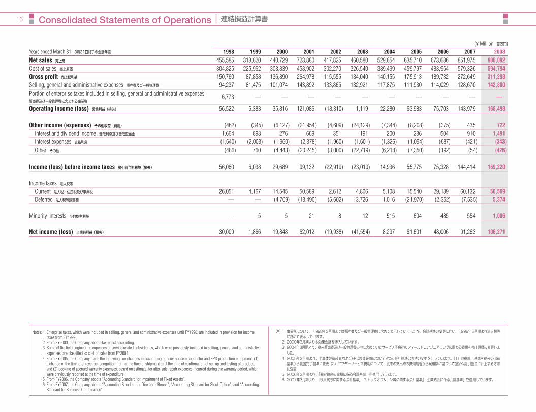
16 Consolidated Statements of Operations 連結損益計算書
(¥ Million 百万円)Years ended March 31 3月31日終了の会計年度 1998 1999 2000 2001 2002 2003 2004 2005 2006 2007 2008
Net sales 売上高 455,585 313,820 440,729 723,880 417,825 460,580 529,654 635,710 673,686 851,975 906,092Cost of sales 売上原価 304,825 225,962 303,839 458,902 302,270 326,540 389,499 459,797 483,954 579,326 594,794Gross profit 売上総利益 150,760 87,858 136,890 264,978 115,555 134,040 140,155 175,913 189,732 272,649 311,298Selling, general and administrative expenses 販売費及び一般管理費 94,237 81,475 101,074 143,892 133,865 132,921 117,875 111,930 114,029 128,670 142,800Portion of enterprise taxes included in selling, general and administrative expenses 販売費及び一般管理費に含まれる事業税
6,773 — — — — — — — — — —
Operating income (loss) 営業利益(損失) 56,522 6,383 35,816 121,086 (18,310) 1,119 22,280 63,983 75,703 143,979 168,498
Other income (expenses) その他収益(費用) (462) (345) (6,127) (21,954) (4,609) (24,129) (7,344) (8,208) (375) 435 722Interest and dividend income 受取利息及び受取配当金 1,664 898 276 669 351 191 200 236 504 910 1,491Interest expenses 支払利息 (1,640) (2,003) (1,960) (2,378) (1,960) (1,601) (1,326) (1,094) (687) (421) (343)Other その他 (486) 760 (4,443) (20,245) (3,000) (22,719) (6,218) (7,350) (192) (54) (426)
Income (loss) before income taxes 税引前当期利益(損失) 56,060 6,038 29,689 99,132 (22,919) (23,010) 14,936 55,775 75,328 144,414 169,220
Income taxes 法人税等
Current 法人税・住民税及び事業税 26,051 4,167 14,545 50,589 2,612 4,806 5,108 15,540 29,189 60,132 56,569Deferred 法人税等調整額 — — (4,709) (13,490) (5,602) 13,726 1,016 (21,970) (2,352) (7,535) 5,374
Minority interests 少数株主利益 — 5 5 21 8 12 515 604 485 554 1,006
Net income (loss) 当期純利益(損失) 30,009 1,866 19,848 62,012 (19,938) (41,554) 8,297 61,601 48,006 91,263 106,271
Notes: 1. Enterprise taxes, which were included in selling, general and administrative expenses until FY1998, are included in provision for income taxes from FY1999.
2. From FY2000, the Company adopts tax-effect accounting. 3. Some of the field engineering expenses of service related subsidiaries, which were previously included in selling, general and administrative
expenses, are classified as cost of sales from FY2004. 4. From FY2005, the Company made the following two changes in accounting policies for semiconductor and FPD production equipment: (1)
a change of the timing of revenue recognition from at the time of shipment to at the time of confirmation of set-up and testing of products and (2) booking of accrued warranty expenses, based on estimate, for after-sale repair expenses incurred during the warranty period, which were previously reported at the time of expenditure.
5. From FY2006, the Company adopts “Accounting Standard for Impairment of Fixed Assets”. 6. From FY2007, the Company adopts “Accounting Standard for Director’s Bonus”, “Accounting Standard for Stock Option”, and “Accounting
Standard for Business Combination”
注) 1. 事業税について、1998年3月期までは販売費及び一般管理費に含めて表示していましたが、会計基準の変更に伴い、1999年3月期より法人税等に含めて表示しています。
2. 2000年3月期より税効果会計を導入しています。 3. 2004年3月期より、従来販売費及び一般管理費の中に含めていたサービス子会社のフィールドエンジニアリングに関わる費用を売上原価に変更しま
した。 4. 2005年3月期より、半導体製造装置およびFPD製造装置について2つの会計処理の方法の変更を行っています。(1)収益計上基準を従来の出荷
基準から設置完了基準に変更(2)アフターサービス費用について、従来の支出時の費用処理から見積額に基づいて製品保証引当金に計上する方法に変更
5. 2006年3月期より、「固定資産の減損に係る会計基準」を適用しています。 6. 2007年3月期より、「役員賞与に関する会計基準」「ストックオプション等に関する会計基準」「企業結合に係る会計基準」を適用しています。
010_0454002472006.indd 16 2008/07/11 16:38:30
17
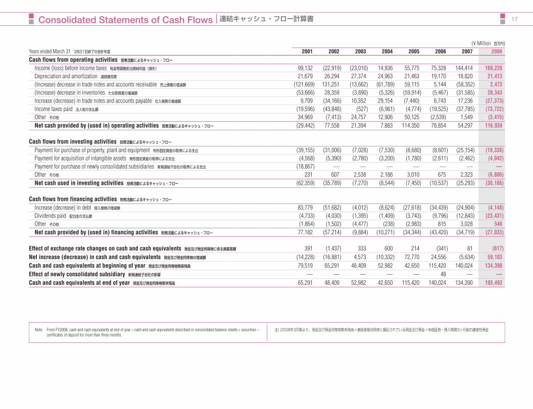
Note: From FY2008, cash and cash equivalents at end of year = cash and cash equivalents described in consolidated balance sheets + securities – certificates of deposit for more than three months.
注) 2008年3月期より、現金及び現金同等物期末残高=連結貸借対照表に掲記されている現金及び預金+有価証券−預入期間3ヶ月超の譲渡性預金
Consolidated Statements of Cash Flows 連結キャッシュ・フロー計算書
(¥ Million 百万円)Years ended March 31 3月31日終了の会計年度 2001 2002 2003 2004 2005 2006 2007 2008
Cash flows from operating activities 営業活動によるキャッシュ・フロー
Income (loss) before income taxes 税金等調整前当期純利益(損失) 99,132 (22,919) (23,010) 14,936 55,775 75,328 144,414 169,220Depreciation and amortization 減価償却費 21,679 26,294 27,374 24,963 21,463 19,170 18,820 21,413(Increase) decrease in trade notes and accounts receivable 売上債権の増減額 (121,669) 131,251 (13,662) (61,789) 59,115 5,144 (58,352) 2,473(Increase) decrease in inventories たな卸資産の増減額 (53,666) 28,359 (3,890) (5,326) (59,914) (5,467) (31,585) 28,343Increase (decrease) in trade notes and accounts payable 仕入債務の増減額 9,709 (34,166) 10,352 29,154 (7,440) 6,743 17,236 (27,373)Income taxes paid 法人税の支払額 (19,596) (43,848) (527) (6,961) (4,774) (19,525) (37,785) (73,722)Other その他 34,969 (7,413) 24,757 12,906 50,125 (2,539) 1,549 (3,415)Net cash provided by (used in) operating activities 営業活動によるキャッシュ・フロー (29,442) 77,558 21,394 7,883 114,350 78,854 54,297 116,939
Cash flows from investing activities 投資活動によるキャッシュ・フロー
Payment for purchase of property, plant and equipment 有形固定資産の取得による支出 (39,155) (31,006) (7,028) (7,530) (8,680) (8,601) (25,154) (19,338)Payment for acquisition of intangible assets 無形固定資産の取得による支出 (4,568) (5,390) (2,780) (3,200) (1,780) (2,611) (2,462) (4,042)Payment for purchase of newly consolidated subsidiaries 新規連結子会社の取得による支出 (18,867) — — — — — — —Other その他 231 607 2,538 2,186 3,010 675 2,323 (6,806)Net cash used in investing activities 投資活動によるキャッシュ・フロー (62,359) (35,789) (7,270) (8,544) (7,450) (10,537) (25,293) (30,186)
Cash flows from financing activities 財務活動によるキャッシュ・フロー
Increase (decrease) in debt 借入債務の増減額 83,779 (51,682) (4,012) (8,624) (27,618) (34,439) (24,904) (4,148)Dividends paid 配当金の支払額 (4,733) (4,030) (1,395) (1,409) (3,743) (9,796) (12,843) (23,431)Other その他 (1,864) (1,502) (4,477) (238) (2,983) 815 3,028 546Net cash provided by (used in) financing activities 財務活動によるキャッシュ・フロー 77,182 (57,214) (9,884) (10,271) (34,344) (43,420) (34,719) (27,033)
Effect of exchange rate changes on cash and cash equivalents 現金及び現金同等物に係る換算差額 391 (1,437) 333 600 214 (341) 81 (617)Net increase (decrease) in cash and cash equivalents 現金及び現金同等物の増減額 (14,228) (16,881) 4,573 (10,332) 72,770 24,556 (5,634) 59,103Cash and cash equivalents at beginning of year 現金及び現金同等物期首残高 79,519 65,291 48,409 52,982 42,650 115,420 140,024 134,390Effect of newly consolidated subsidiary 新規連結子会社の影響 — — — — — 48 — —Cash and cash equivalents at end of year 現金及び現金同等物期末残高 65,291 48,409 52,982 42,650 115,420 140,024 134,390 193,493
010_0454002472006.indd 17 2008/07/11 16:38:30
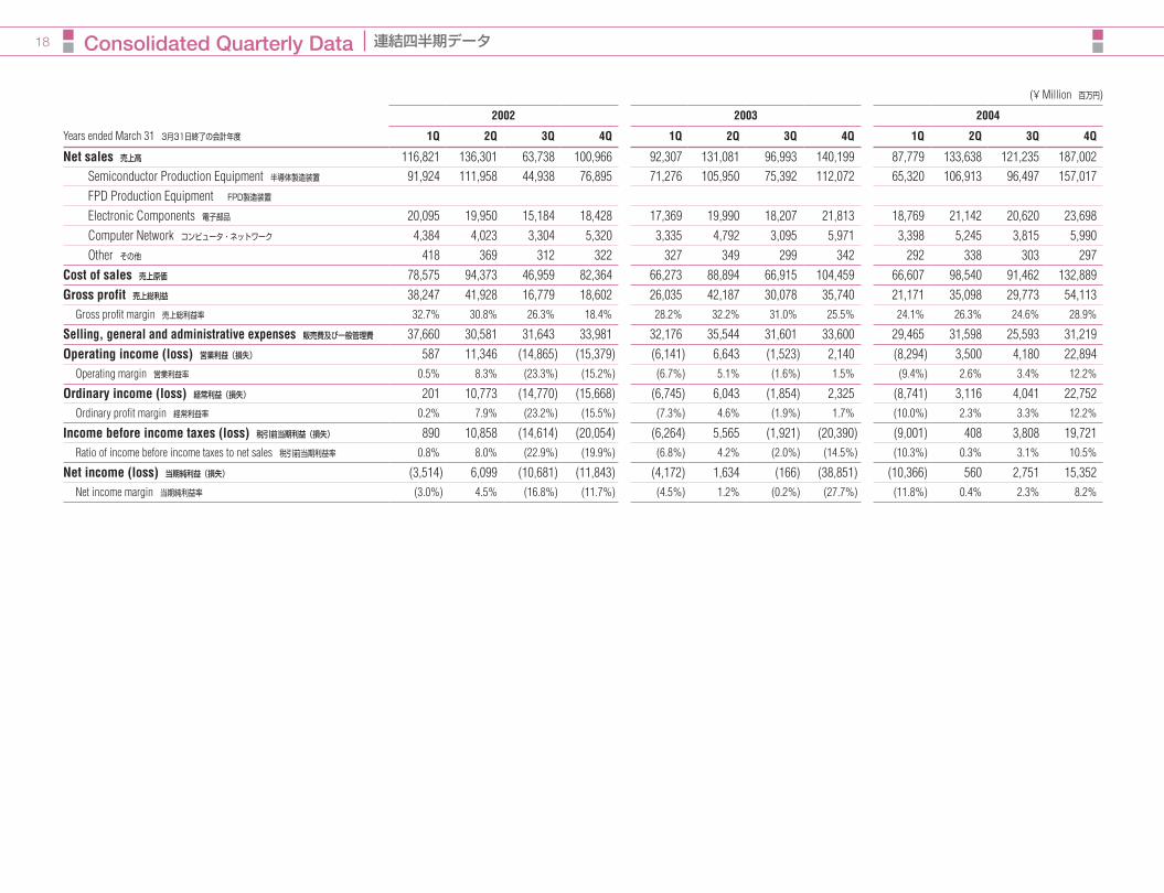
18 Consolidated Quarterly Data 連結四半期データ
(¥ Million 百万円)
2002 2003 2004
Years ended March 31 3月31日終了の会計年度 1Q 2Q 3Q 4Q 1Q 2Q 3Q 4Q 1Q 2Q 3Q 4Q
Net sales 売上高 116,821 136,301 63,738 100,966 92,307 131,081 96,993 140,199 87,779 133,638 121,235 187,002Semiconductor Production Equipment 半導体製造装置 91,924 111,958 44,938 76,895 71,276 105,950 75,392 112,072 65,320 106,913 96,497 157,017FPD Production Equipment FPD製造装置 16,530 18,552 14,248 19,687 14,605 16,230 87,779 133,638 121,235 187,002Electronic Components 電子部品 20,095 19,950 15,184 18,428 17,369 19,990 18,207 21,813 18,769 21,142 20,620 23,698Computer Network コンピュータ・ネットワーク 4,384 4,023 3,304 5,320 3,335 4,792 3,095 5,971 3,398 5,245 3,815 5,990Other その他 418 369 312 322 327 349 299 342 292 338 303 297
Cost of sales 売上原価 78,575 94,373 46,959 82,364 66,273 88,894 66,915 104,459 66,607 98,540 91,462 132,889Gross profit 売上総利益 38,247 41,928 16,779 18,602 26,035 42,187 30,078 35,740 21,171 35,098 29,773 54,113
Gross profit margin 売上総利益率 32.7% 30.8% 26.3% 18.4% 28.2% 32.2% 31.0% 25.5% 24.1% 26.3% 24.6% 28.9%
Selling, general and administrative expenses 販売費及び一般管理費 37,660 30,581 31,643 33,981 32,176 35,544 31,601 33,600 29,465 31,598 25,593 31,219Operating income (loss) 営業利益(損失) 587 11,346 (14,865) (15,379) (6,141) 6,643 (1,523) 2,140 (8,294) 3,500 4,180 22,894
Operating margin 営業利益率 0.5% 8.3% (23.3%) (15.2%) (6.7%) 5.1% (1.6%) 1.5% (9.4%) 2.6% 3.4% 12.2%
Ordinary income (loss) 経常利益(損失) 201 10,773 (14,770) (15,668) (6,745) 6,043 (1,854) 2,325 (8,741) 3,116 4,041 22,752Ordinary profit margin 経常利益率 0.2% 7.9% (23.2%) (15.5%) (7.3%) 4.6% (1.9%) 1.7% (10.0%) 2.3% 3.3% 12.2%
Income before income taxes (loss) 税引前当期利益(損失) 890 10,858 (14,614) (20,054) (6,264) 5,565 (1,921) (20,390) (9,001) 408 3,808 19,721Ratio of income before income taxes to net sales 税引前当期利益率 0.8% 8.0% (22.9%) (19.9%) (6.8%) 4.2% (2.0%) (14.5%) (10.3%) 0.3% 3.1% 10.5%
Net income (loss) 当期純利益(損失) (3,514) 6,099 (10,681) (11,843) (4,172) 1,634 (166) (38,851) (10,366) 560 2,751 15,352Net income margin 当期純利益率 (3.0%) 4.5% (16.8%) (11.7%) (4.5%) 1.2% (0.2%) (27.7%) (11.8%) 0.4% 2.3% 8.2%
010_0454002472006.indd 18 2008/07/11 16:38:30
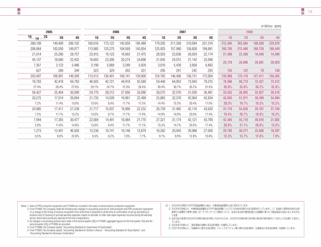
19
(¥ Million 百万円)
2005 2006 2007 20081Q 2Q 3Q 4Q 1Q 2Q 3Q 4Q 1Q 2Q 3Q 4Q 1Q 2Q 3Q 4Q
280,199 149,409 206,102 160,016 173,122 145,059 195,489 179,205 211,358 210,094 251,319 212,494 263,884 199,838 229,876206,064 102,050 149,077 113,985 125,275 104,569 143,054 125,925 157,980 158,828 199,891 165,785 213,466 160,739 186,44921,014 25,266 28,757 23,915 19,123 16,663 21,475 28,933 23,636 26,024 22,174 21,400 22,200 10,048 14,36845,137 18,680 22,432 18,603 23,306 20,274 24,698 21,042 24,012 21,142 22,098
25,176 28,096 28,981 28,9297,357 3,123 5,486 3,190 5,089 3,289 5,929 3,010 5,439 3,858 6,863
627 289 349 323 329 263 331 295 291 242 293 133 122 70 130203,497 106,991 149,309 113,513 130,401 100,141 139,900 124,765 146,406 136,151 172,004 135,908 175,110 127,411 156,36576,703 42,418 56,793 46,503 42,721 44,918 55,589 54,440 64,952 73,943 79,315 76,586 88,773 72,427 73,51227.4% 28.4% 27.6% 29.1% 24.7% 31.0% 28.4% 30.4% 30.7% 35.2% 31.6% 36.0% 33.6% 36.2% 32.0%
56,427 25,404 30,099 24,770 28,212 27,956 33,090 28,575 32,576 31,039 36,481 33,552 36,803 33,927 38,51820,275 17,014 26,694 21,733 14,509 16,961 22,499 25,865 32,376 42,904 42,834 43,035 51,971 38,499 34,994
7.2% 11.4% 13.0% 13.6% 8.4% 11.7% 11.5% 14.4% 15.3% 20.4% 17.0% 20.3% 19.7% 19.3% 15.2%20,985 17,411 27,238 21,717 15,037 16,966 22,232 26,739 31,465 42,116 43,620 41,176 54,620 39,761 37,156
7.5% 11.7% 13.2% 13.6% 8.7% 11.7% 11.4% 14.9% 14.9% 20.0% 17.4% 19.4% 20.7% 19.9% 16.2%7,944 17,355 30,477 22,084 14,491 16,984 21,770 27,321 31,174 42,121 43,799 42,484 55,718 40,016 31,0022.8% 11.6% 14.8% 13.8% 8.4% 11.7% 11.1% 15.2% 14.7% 20.0% 17.4% 20.0% 21.1% 20.0% 13.5%
1,273 13,401 46,928 13,238 10,741 10,148 13,879 16,282 20,943 26,988 27,050 26,193 36,271 25,600 18,2070.5% 9.0% 22.8% 8.3% 6.2% 7.0% 7.1% 9.1% 9.9% 12.8% 10.8% 12.3% 13.7% 12.8% 7.9%
1H
Notes: 1. Sales of FPD production equipment until FY2004 are included in the sales of semiconductor production equipment. 2. From FY2005, the Company made the following two changes in accounting policies for semiconductor and FPD production equipment:
(1) a change of the timing of revenue recognition from at the time of shipment to at the time of confirmation of set-up and testing of products and (2) booking of accrued warranty expenses, based on estimate, for after-sale repair expenses incurred during the warranty period, which were previously reported at the time of expenditure.
3. As changes in accounting policies were made in the second quarter (2Q) of FY2005, aggregate figures for the first quarter (1Q) and the second quarter (2Q) of FY2005 are provided.
4. From FY2006, the Company adopts “Accounting Standard for Impairment of Fixed Assets”. 5. From FY2007, the Company adopts “Accounting Standard for Director’s Bonus”, “Accounting Standard for Stock Option”, and
“Accounting Standard for Business Combination”
注) 1. 2004年3月期までのFPD製造装置売上高は、半導体製造装置売上高に含まれています。 2. 2005年3月期より、半導体製造装置およびFPD製造装置について2つの会計処理の方法の変更を行っています。(1)収益計上基準を従来の出荷
基準から設置完了基準に変更(2)アフターサービス費用について、従来の支出時の費用処理から見積額に基づいて製品保証引当金に計上する方法に変更
3. 会計方針の変更が2005年3月期の第2四半期に行なわれたため、2005年3月期の第1四半期と第2四半期の数字につきましては合算にて表示しています。
4. 2006年3月期より、「固定資産の減損に係る会計基準」を適用しています。 5. 2007年3月期より、「役員賞与に関する会計基準」「ストックオプション等に関する会計基準」「企業結合に係る会計基準」を適用しています。
010_0454002472006.indd 19 2008/07/11 16:38:31

20 Stock Information 株式情報
■ Stock Price Range 株価の推移
Years ended March 31 各3月31日までの1年間 1998 1999 2000 2001 2002 2003 2004 2005 2006 2007 2008High (¥) 高値(円) 8,670 6,630 18,000 20,090 10,260 10,280 8,920 7,390 9,270 9,650 9,410Low (¥) 安値(円) 3,920 2,755 6,080 6,240 3,820 3,870 4,070 5,110 5,350 6,980 5,540Note: Prices have been adjusted to reflect stock splits. 注) 株式分割調整後の株価
PER (Times) High 株価収益率(倍) 最高 49.6 619.6 158.5 56.8 — — 192.4 21.5 34.6 18.9 15.8Low 最低 22.4 257.5 53.6 17.6 — — 87.8 14.9 20.0 13.7 9.3
PBR (Times) High 株価純資産倍率(倍) 最高 5.8 4.5 11.5 10.6 5.8 7.1 5.8 4.0 4.4 3.7 3.1Low 最低 2.6 1.9 3.9 3.3 2.2 2.7 2.6 2.7 2.5 2.7 1.9
PCFR (Times) High 株価キャッシュ・フロー倍率(倍) 最高 34.9 58.4 80.1 42.1 282.6 — 47.4 15.9 24.6 15.6 13.2Low 最低 15.8 24.3 27.1 13.1 105.2 — 21.6 11.0 14.2 11.3 7.8
Price / earnings ratio = Common stock price / Net income per share 株価収益率 = 株価 ÷ 1株当り当期純利益Price / book value ratio = Common stock price / Net assets per share 株価純資産倍率 = 株価 ÷ 1株当り純資産Price / cash flow ratio = Common stock price / Cash flow per share 株価キャッシュ・フロー倍率 = 株価 ÷ 1株当りキャッシュ・フロー
■ Number of Shares Issued (Fiscal Year-End) 発行済株式数の推移(期末)
FY 年度 1998 1999 2000 2001 2002 2003 2004 2005 2006 2007 2008Number of shares issued (Thousands) 発行済株式数(千株) 174,569 174,624 175,660 175,691 175,691 175,698 180,611 180,611 180,611 180,611 180,611Market capitalization (¥ Billion) 時価総額(十億円) 783.8 1,070.4 2,722.7 1,454.7 1,583.0 815.2 1,255.2 1,103.5 1,466.6 1,488.2 1,094.5Market capitalization = Closing stock price at fiscal year-end × Number of shares issued 時価総額 = 期末株式終値 × 発行済株式数
■ Public Offering of Common Stock 公募増資の実績
Public Offering of Common Stock 有償・公募
Date of issue発行年月日
Subscribed shares(Thousands)
発行株式数(千株)
Issuing price(¥)
発行価格(円)June 2, 1980 1980年6月2日 4,131 1,540July 1, 1981 1981年7月1日 2,000 4,730October 16, 1982 1982年10月16日 4,000 3,050May 6, 1983 1983年5月6日 20 2,550June 23, 1984 1984年6月23日 3,000 4,015November 15, 1989 1989年11月15日 6,000 3,233
Stock Splits 株式分割
Date of issue発行年月日
Ratio of distribution分割比率
October 1, 1980 1980年10月1日 1:1.25October 1, 1981 1981年10月1日 1:1.3November 20, 1982 1982年11月20日 1:1.3February 1, 1983 1983年2月1日 1:2.0November 20, 1984 1984年11月20日 1:1.2November 15, 1989 1989年11月15日 1:1.1November 15, 1990 1990年11月15日 1:1.2May 20, 1997 1997年5月20日 1:1.1
22,000
16,500
11,000
5,500
(¥ 円)
(Calendar year 暦年)
Note: Prices have been adjusted to reflect stock splits. 注) 株式分割調整後の株価
I II III IV2006
I II III IV I II III IV I II III IV I II III IV I II III IV I II III IV I II III IV I II III IV I1998 1999 2000 2001 2002 2003 2004 2005
II III IV I2007 2008
I
010_0454002472006.indd 20 2008/07/11 16:38:31

21
■ Major Shareholders (Top 10) 大株主一覧(上位10位)As of March 31, 2008 2008年3月31日現在
■ Composition of Shareholders by Category 所有者別分布状況As of March 31, 2008 2008年3月31日現在
2004 2005 2006 2007 2008
Category区分
Number of shareholders/Shares (Thousands)/Composition
Number of shareholders/Shares (Thousands)/Composition
Number of shareholders/Shares (Thousands)/Composition
Number of shareholders/Shares (Thousands)/Composition
Number of shareholders/Shares (Thousands)/Composition
株主数 株式数(千株) 構成比 株主数 株式数(千株) 構成比 株主数 株式数(千株) 構成比 株主数 株式数(千株) 構成比 株主数 株式数(千株) 構成比Japanese financial institutions and securities companies 金融機関・証券会社 232 73,221 40.5% 207 66,817 37.0% 202 57,748 32.0% 256 81,793 45.3% 262 79,240 43.9%Foreign institutions and others 外国法人等 571 66,604 36.9% 553 74,864 41.5% 600 90,081 49.9% 623 68,775 38.1% 639 72,365 40.1%Japanese individuals and others 個人・その他 59,361 23,251 12.9% 59,415 23,902 13.2% 44,930 18,408 10.2% 39,837 16,247 9.0% 41,871 16,739 9.3%Other Japanese corporations その他の法人 708 15,513 8.6% 681 12,498 6.9% 539 12,037 6.6% 572 11,983 6.6% 551 10,588 5.8%Treasury stock 自己株式 1 2,022 1.1% 1 2,530 1.4% 1 2,336 1.3% 1 1,813 1.0% 1 1,679 0.9%Total 合計 60,873 180,611 100.0% 60,857 180,611 100.0% 46,272 180,611 100.0% 41,289 180,611 100.0% 43,324 180,611 100.0%
Name株主名
Shares (Thousands)所有株式数(千株)
Percentage持株比率(%)
The Master Trust Bank of Japan, Ltd. (trust account) 日本マスタートラスト信託銀行(信託口) 19,052 10.54Japan Trustee Services Bank, Ltd. (trust account) 日本トラスティ・サービス信託銀行(信託口) 14,423 7.98Tokyo Broadcasting System, Inc. 東京放送 8,727 4.83The Dai-ichi Mutual Life Insurance Company. 第一生命保険相互会社 4,800 2.65Deutsche Securities Inc. ドイツ証券 4,347 2.40
Name株主名
Shares (Thousands)所有株式数(千株)
Percentage持株比率(%)
Nomura Securities Co., Ltd. 野村證券 4,183 2.31Trust & Custody Services Bank, Ltd.(trust account) 資産管理サービス信託銀行(証券投資信託口) 3,488 1.93Japan Trustee Services Bank, Ltd. (trust account 4) 日本トラスティ・サービス信託銀行(信託口4) 3,021 1.67The Bank of Tokyo-Mitsubishi UFJ, Ltd. 三菱東京UFJ銀行 3,000 1.66BNP Paribas Securities(Japan) Ltd. ビー・エヌ・ピー・パリバ・セキュリティーズ(ジャパン)リミテッド(ビーエヌピーパリバ証券会社) 2,790 1.54
Japanese financial institutions and securities companies 金融機関・証券会社Foreign institutions and others 外国法人等Japanese individuals and others 個人・その他Other Japanese corporations その他の法人Treasury stock 自己株式
2007
2006
2005
2004 40.5% 36.9% 12.9% 8.6% 1.1%
2008
37.0% 41.5% 13.2% 6.9% 1.4%
32.0% 49.9% 10.2% 6.6%
45.3% 38.1% 9.0%
1.3%
1.0%6.6%
43.9% 40.1% 9.3% 0.9%5.8%
Number of shareholders and shares includes number of odd lot shareholders and odd lot shares.株主数及び株式数は、単元未満株主数及び単元未満株式数を含んでいます。
010_0454002472006.indd 21 2008/07/11 16:38:32
2008
TOKYO ELECTRON LIMITED
World Headquarters
Akasaka Biz Tower 3-1, Akasaka 5-chomeMinato-ku, Tokyo 107-6325, JapanTel: +81-3-5561-7000Fax: +81-3-5561-7400 URL: http://www.tel.com
Investor RelationsCorporate Communications Dept.
Tel: +81-3-5561-7003Fax: +81-3-5561-7400
C2
1
2
3
4
6
8
10
14
16
17
18
20
目次CONTENTS
TOKYO ELECTRON
As o f March 31 , 2008
FACTBOOK
PR46-133Printed in Japan
本誌は再生紙を使用しています。Printed on recycled paper.
Industry Data インダストリー・データ
Tokyo Electron (TEL) Overview東京エレクトロン(TEL)の事業概要
Global TELTELの世界展開
Topics in Recent Years近年のトピックス
Semiconductor & TFT-LCD Manufacturing Process Flow
半導体製造工程及びTFT-LCD製造工程
Consolidated Operating Results連結業績
Semiconductor Production Equipment (SPE) and
FPD Production Equipment半導体製造装置・FPD製造装置
Consolidated Financial Data連結財務データ
Consolidated Balance Sheets連結貸借対照表
Consolidated Statements of Operations連結損益計算書
Consolidated Statements of Cash Flows連結キャッシュ・フロー計算書
Consolidated Quarterly Data連結四半期データ
Stock Information株式情報
010_0454002472006.indd 1 2008/07/11 16:38:13
Related Documents