TMUX13xx 5-V, Bidirectional 8:1, 1-Channel and 4:1, 2-Channel Multiplexers with Injection Current Control 1 Features • Injection Current Control • Back-Powering Protection – No ESD Diode Path to V DD • Wide Supply Range: 1.62 V to 5.5 V • Low Capacitance • Bidirectional Signal Path • Rail-to-Rail Operation • 1.8 V Logic Compatible • Fail-Safe Logic • Break-Before-Make Switching • Functional Safety-Capable – Documentation Available to Aid Functional Safety System Design • TMUX1308 - Pin Compatible with: – Industry Standard 4051 and 4851 Multiplexers • TMUX1309 - Pin Compatible with: – Industry Standard 4052 and 4852 Multiplexers 2 Applications • Analog and Digital Multiplexing and Demultiplexing • Diagnostics and Monitoring • Data Center Switch • Remote Radio Unit (RRU) • Rack Server • Electricity Meter • Appliances • Air Conditioner Units • Multifunction Printers • String Inverter • IP Network Camera • Currency Counters • Off-highway Vehicles Control Systems 3 Description The TMUX1308 and TMUX1309 are general purpose complementary metal-oxide semiconductor (CMOS) multiplexers (MUX). The TMUX1308 is an 8:1, 1-channel (single-ended) mux, while the TMUX1309 is a 4:1, 2-channel (differential) mux. The devices support bidirectional analog and digital signals on the source (Sx) and drain (Dx) pins ranging from GND to V DD . The TMUX13xx devices have an internal injection current control feature which eliminates the need for external diode and resistor networks typically used to protect the switch and keep the input signals within the supply voltage. The internal injection current control circuitry allows signals on disabled signal paths to exceed the supply voltage without affecting the signal of the enabled signal path. Additionally, the TMUX13xx devices do not have any internal diode path to the supply pin, which eliminates the risk of damaging components connected to the supply pin, or providing unintended power to the supply rail. All logic inputs have 1.8 V logic compatible thresholds, ensuring both TTL and CMOS logic compatibility when operating with a valid supply voltage. Fail-Safe Logic circuitry allows voltages on the control pins to be applied before the supply pin, protecting the device from potential damage. Device Information PART NUMBER (1) PACKAGE BODY SIZE (NOM) TMUX1308 TMUX1309 TSSOP (16) 5.00 mm × 4.40 mm SOT-23-THIN (16) 4.20 mm x 2.00 mm WQFN (16) 3.50 mm x 2.50 mm (1) For all available packages, see the package option addendum at the end of the data sheet. TMUX1308 A0 A1 A2 EN S1 D S2 S3 S4 S5 S6 S7 S0 1-OF-8 DECODER TMUX1309 S0A DB S1A S2A S3A S0B S1B S2B S3B DA A0 A1 EN 1-OF-4 DECODER TMUX1308 and TMUX1309 Block Diagram www.ti.com TMUX1308, TMUX1309 SCDS426D – MARCH 2020 – REVISED NOVEMBER 2020 Copyright © 2020 Texas Instruments Incorporated Submit Document Feedback 1 Product Folder Links: TMUX1308 TMUX1309 TMUX1308, TMUX1309 SCDS426D – MARCH 2020 – REVISED NOVEMBER 2020 An IMPORTANT NOTICE at the end of this data sheet addresses availability, warranty, changes, use in safety-critical applications, intellectual property matters and other important disclaimers. PRODUCTION DATA.

Welcome message from author
This document is posted to help you gain knowledge. Please leave a comment to let me know what you think about it! Share it to your friends and learn new things together.
Transcript
TMUX13xx 5-V, Bidirectional 8:1, 1-Channel and 4:1, 2-ChannelMultiplexers with Injection Current Control
1 Features• Injection Current Control• Back-Powering Protection
– No ESD Diode Path to VDD• Wide Supply Range: 1.62 V to 5.5 V• Low Capacitance• Bidirectional Signal Path• Rail-to-Rail Operation• 1.8 V Logic Compatible• Fail-Safe Logic• Break-Before-Make Switching• Functional Safety-Capable
– Documentation Available to Aid FunctionalSafety System Design
• TMUX1308 - Pin Compatible with:– Industry Standard 4051 and 4851 Multiplexers
• TMUX1309 - Pin Compatible with:– Industry Standard 4052 and 4852 Multiplexers
2 Applications• Analog and Digital Multiplexing and Demultiplexing• Diagnostics and Monitoring• Data Center Switch• Remote Radio Unit (RRU)• Rack Server• Electricity Meter• Appliances• Air Conditioner Units• Multifunction Printers• String Inverter• IP Network Camera• Currency Counters• Off-highway Vehicles Control Systems
3 DescriptionThe TMUX1308 and TMUX1309 are general purposecomplementary metal-oxide semiconductor (CMOS)multiplexers (MUX). The TMUX1308 is an 8:1,1-channel (single-ended) mux, while the TMUX1309is a 4:1, 2-channel (differential) mux. The devicessupport bidirectional analog and digital signals on thesource (Sx) and drain (Dx) pins ranging from GND toVDD.
The TMUX13xx devices have an internal injectioncurrent control feature which eliminates the need forexternal diode and resistor networks typically used toprotect the switch and keep the input signals withinthe supply voltage. The internal injection currentcontrol circuitry allows signals on disabled signalpaths to exceed the supply voltage without affectingthe signal of the enabled signal path. Additionally, theTMUX13xx devices do not have any internal diodepath to the supply pin, which eliminates the risk ofdamaging components connected to the supply pin, orproviding unintended power to the supply rail.
All logic inputs have 1.8 V logic compatiblethresholds, ensuring both TTL and CMOS logiccompatibility when operating with a valid supplyvoltage. Fail-Safe Logic circuitry allows voltages onthe control pins to be applied before the supply pin,protecting the device from potential damage.
Device InformationPART NUMBER(1) PACKAGE BODY SIZE (NOM)
TMUX1308TMUX1309
TSSOP (16) 5.00 mm × 4.40 mm
SOT-23-THIN (16) 4.20 mm x 2.00 mm
WQFN (16) 3.50 mm x 2.50 mm
(1) For all available packages, see the package optionaddendum at the end of the data sheet.
TMUX1308
A0 A1 A2 EN
S1
D
S2
S3
S4
S5
S6
S7
S0
1-OF-8
DECODER
TMUX1309
S0A
DB
S1A
S2A
S3A
S0B
S1B
S2B
S3B
DA
A0 A1 EN
1-OF-4
DECODER
TMUX1308 and TMUX1309 Block Diagram
www.ti.comTMUX1308, TMUX1309
SCDS426D – MARCH 2020 – REVISED NOVEMBER 2020
Copyright © 2020 Texas Instruments Incorporated Submit Document Feedback 1
Product Folder Links: TMUX1308 TMUX1309
TMUX1308, TMUX1309SCDS426D – MARCH 2020 – REVISED NOVEMBER 2020
An IMPORTANT NOTICE at the end of this data sheet addresses availability, warranty, changes, use in safety-critical applications,intellectual property matters and other important disclaimers. PRODUCTION DATA.
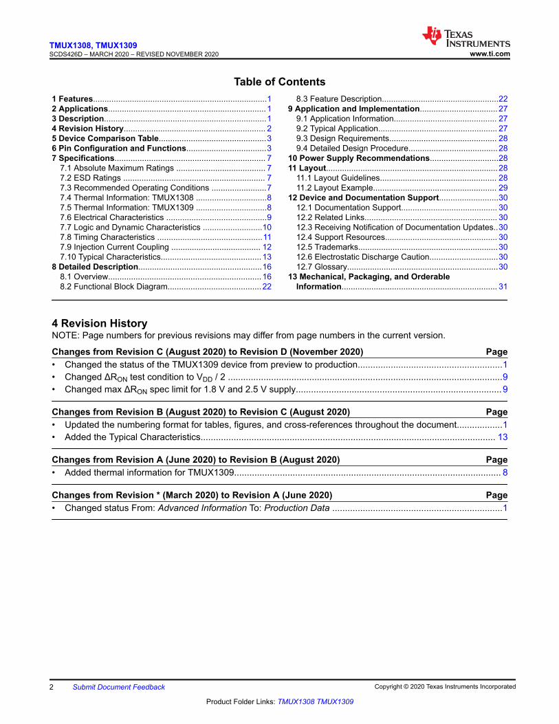
Table of Contents1 Features............................................................................12 Applications..................................................................... 13 Description.......................................................................14 Revision History.............................................................. 25 Device Comparison Table...............................................36 Pin Configuration and Functions...................................37 Specifications.................................................................. 7
7.1 Absolute Maximum Ratings ....................................... 77.2 ESD Ratings .............................................................. 77.3 Recommended Operating Conditions ........................77.4 Thermal Information: TMUX1308 ...............................87.5 Thermal Information: TMUX1309 ...............................87.6 Electrical Characteristics ............................................97.7 Logic and Dynamic Characteristics ..........................107.8 Timing Characteristics ..............................................117.9 Injection Current Coupling ....................................... 127.10 Typical Characteristics............................................ 13
8 Detailed Description......................................................168.1 Overview................................................................... 168.2 Functional Block Diagram......................................... 22
8.3 Feature Description...................................................229 Application and Implementation.................................. 27
9.1 Application Information............................................. 279.2 Typical Application.................................................... 279.3 Design Requirements............................................... 289.4 Detailed Design Procedure....................................... 28
10 Power Supply Recommendations..............................2811 Layout...........................................................................28
11.1 Layout Guidelines................................................... 2811.2 Layout Example...................................................... 29
12 Device and Documentation Support..........................3012.1 Documentation Support.......................................... 3012.2 Related Links.......................................................... 3012.3 Receiving Notification of Documentation Updates..3012.4 Support Resources................................................. 3012.5 Trademarks.............................................................3012.6 Electrostatic Discharge Caution..............................3012.7 Glossary..................................................................30
13 Mechanical, Packaging, and OrderableInformation.................................................................... 31
4 Revision HistoryNOTE: Page numbers for previous revisions may differ from page numbers in the current version.
Changes from Revision C (August 2020) to Revision D (November 2020) Page• Changed the status of the TMUX1309 device from preview to production.........................................................1• Changed ΔRON test condition to VDD / 2 ............................................................................................................9• Changed max ΔRON spec limit for 1.8 V and 2.5 V supply.................................................................................9
Changes from Revision B (August 2020) to Revision C (August 2020) Page• Updated the numbering format for tables, figures, and cross-references throughout the document..................1• Added the Typical Characteristics.................................................................................................................... 13
Changes from Revision A (June 2020) to Revision B (August 2020) Page• Added thermal information for TMUX1309......................................................................................................... 8
Changes from Revision * (March 2020) to Revision A (June 2020) Page• Changed status From: Advanced Information To: Production Data ...................................................................1
TMUX1308, TMUX1309SCDS426D – MARCH 2020 – REVISED NOVEMBER 2020 www.ti.com
2 Submit Document Feedback Copyright © 2020 Texas Instruments Incorporated
Product Folder Links: TMUX1308 TMUX1309
5 Device Comparison TablePRODUCT DESCRIPTIONTMUX1308 8:1, 1-Channel, single-ended multiplexer
TMUX1309 4:1, 2-Channel, differential multiplexer
6 Pin Configuration and Functions
1S4 16 VDD
2S6 15 S2
3D 14 S1
4S7 13 S0
5S5 12 S3
6 11 A0
7N.C. 10 A1
8GND 9 A2
Not to scale
Figure 6-1. TMUX1308: PW Package 16-Pin TSSOPTop View
1S4 16 VDD
2S6 15 S2
3D 14 S1
4S7 13 S0
5S5 12 S3
6 11 A0
7N.C. 10 A1
8GND 9 A2
Not to scale
Figure 6-2. TMUX1308: DYY Package 16-PinSOT-23-THIN Top View
Thermal
Pad
2S6
3D
4S7
5S5
6
7N.C.
8G
ND
9A
2
10 A1
11 A0
12 S3
13 S0
14 S1
15 S2
16
VD
D
1S
4
Not to scale
Figure 6-3. TMUX1308: BQB Package 16-Pin WQFN Top View
www.ti.comTMUX1308, TMUX1309
SCDS426D – MARCH 2020 – REVISED NOVEMBER 2020
Copyright © 2020 Texas Instruments Incorporated Submit Document Feedback 3
Product Folder Links: TMUX1308 TMUX1309
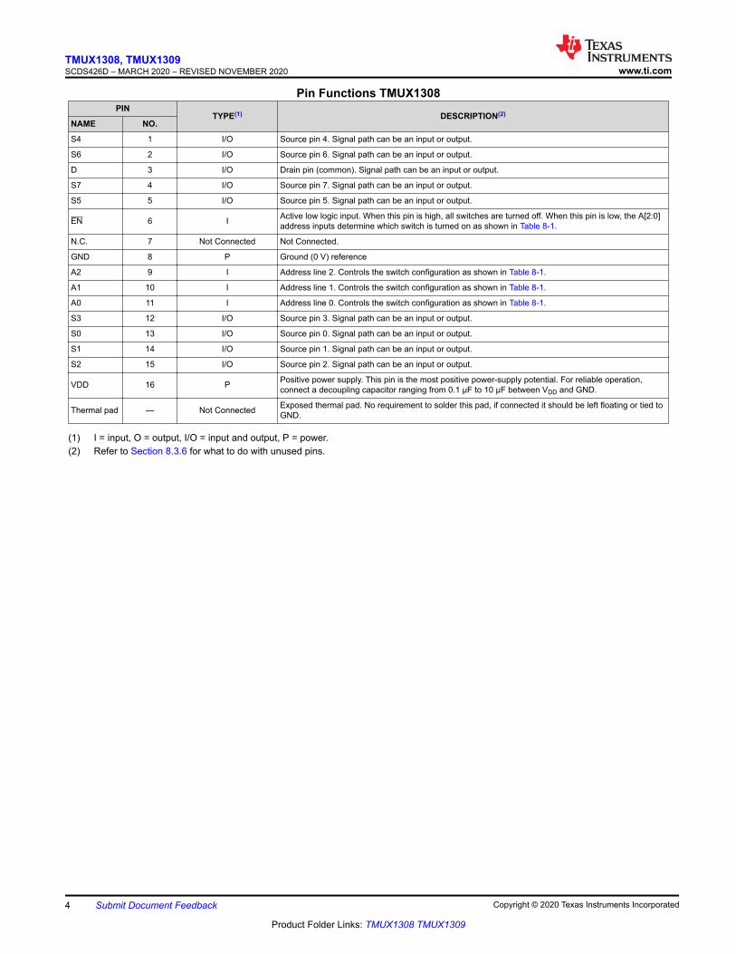
Pin Functions TMUX1308PIN
TYPE(1) DESCRIPTION(2)NAME NO.
S4 1 I/O Source pin 4. Signal path can be an input or output.
S6 2 I/O Source pin 6. Signal path can be an input or output.
D 3 I/O Drain pin (common). Signal path can be an input or output.
S7 4 I/O Source pin 7. Signal path can be an input or output.
S5 5 I/O Source pin 5. Signal path can be an input or output.
EN 6 I Active low logic input. When this pin is high, all switches are turned off. When this pin is low, the A[2:0]address inputs determine which switch is turned on as shown in Table 8-1.
N.C. 7 Not Connected Not Connected.
GND 8 P Ground (0 V) reference
A2 9 I Address line 2. Controls the switch configuration as shown in Table 8-1.
A1 10 I Address line 1. Controls the switch configuration as shown in Table 8-1.
A0 11 I Address line 0. Controls the switch configuration as shown in Table 8-1.
S3 12 I/O Source pin 3. Signal path can be an input or output.
S0 13 I/O Source pin 0. Signal path can be an input or output.
S1 14 I/O Source pin 1. Signal path can be an input or output.
S2 15 I/O Source pin 2. Signal path can be an input or output.
VDD 16 P Positive power supply. This pin is the most positive power-supply potential. For reliable operation,connect a decoupling capacitor ranging from 0.1 µF to 10 µF between VDD and GND.
Thermal pad — Not Connected Exposed thermal pad. No requirement to solder this pad, if connected it should be left floating or tied toGND.
(1) I = input, O = output, I/O = input and output, P = power.(2) Refer to Section 8.3.6 for what to do with unused pins.
TMUX1308, TMUX1309SCDS426D – MARCH 2020 – REVISED NOVEMBER 2020 www.ti.com
4 Submit Document Feedback Copyright © 2020 Texas Instruments Incorporated
Product Folder Links: TMUX1308 TMUX1309
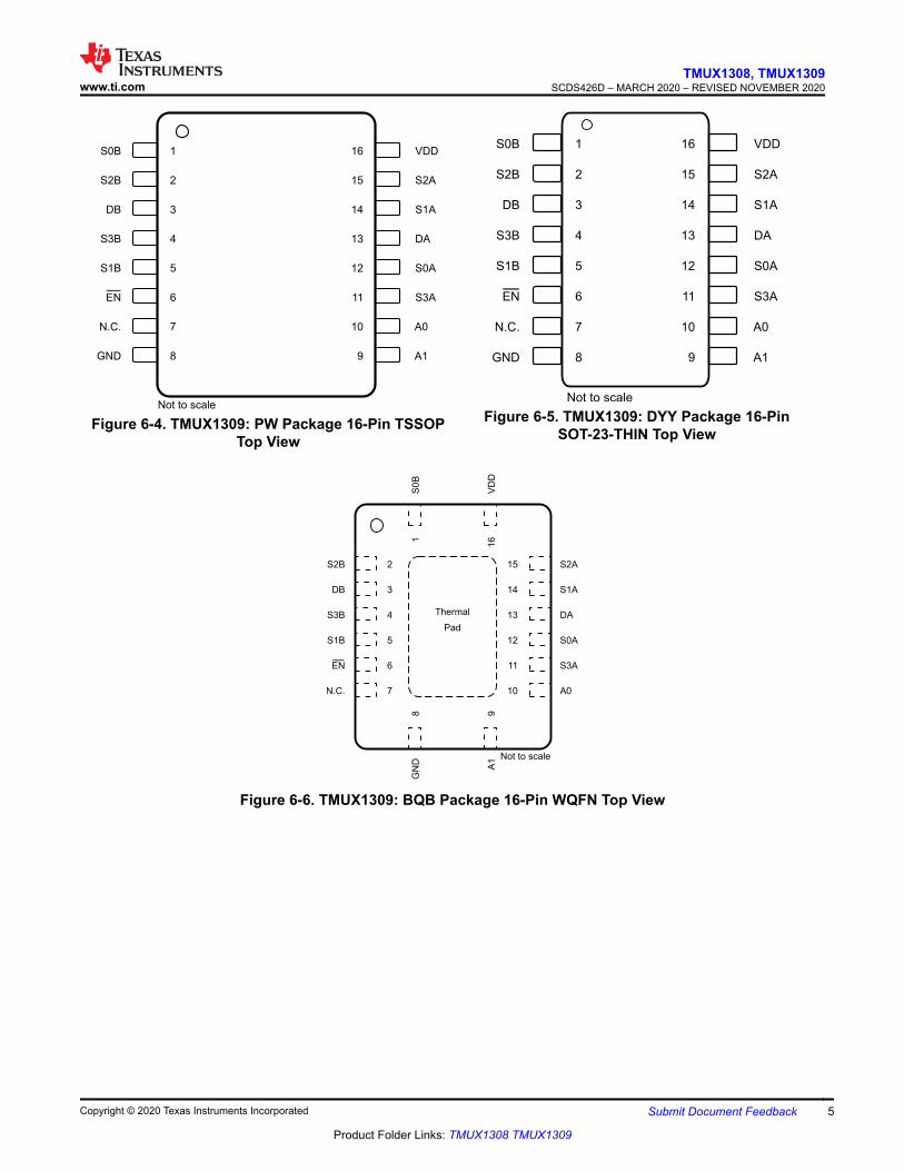
1S0B 16 VDD
2S2B 15 S2A
3DB 14 S1A
4S3B 13 DA
5S1B 12 S0A
6 11 S3A
7N.C. 10 A0
8GND 9 A1
Not to scale
Figure 6-4. TMUX1309: PW Package 16-Pin TSSOPTop View
1S0B 16 VDD
2S2B 15 S2A
3DB 14 S1A
4S3B 13 DA
5S1B 12 S0A
6 11 S3A
7N.C. 10 A0
8GND 9 A1
Not to scale
Figure 6-5. TMUX1309: DYY Package 16-PinSOT-23-THIN Top View
Thermal
Pad
2S2B
3DB
4S3B
5S1B
6
7N.C.
8G
ND
9A
1
10 A0
11 S3A
12 S0A
13 DA
14 S1A
15 S2A
16
VD
D
1S
0B
Not to scale
Figure 6-6. TMUX1309: BQB Package 16-Pin WQFN Top View
www.ti.comTMUX1308, TMUX1309
SCDS426D – MARCH 2020 – REVISED NOVEMBER 2020
Copyright © 2020 Texas Instruments Incorporated Submit Document Feedback 5
Product Folder Links: TMUX1308 TMUX1309
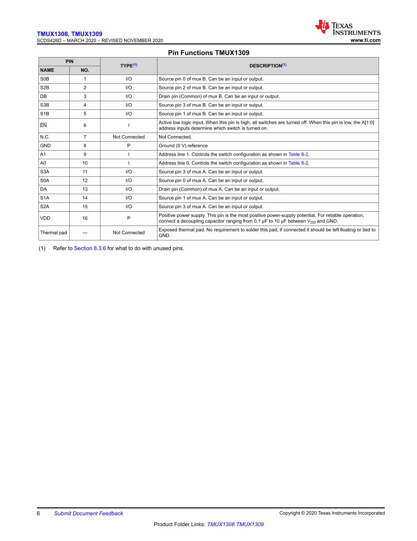
Pin Functions TMUX1309PIN
TYPE(1) DESCRIPTION(1)NAME NO.
S0B 1 I/O Source pin 0 of mux B. Can be an input or output.
S2B 2 I/O Source pin 2 of mux B. Can be an input or output.
DB 3 I/O Drain pin (Common) of mux B. Can be an input or output.
S3B 4 I/O Source pin 3 of mux B. Can be an input or output.
S1B 5 I/O Source pin 1 of mux B. Can be an input or output.
EN 6 I Active low logic input. When this pin is high, all switches are turned off. When this pin is low, the A[1:0]address inputs determine which switch is turned on.
N.C. 7 Not Connected Not Connected.
GND 8 P Ground (0 V) reference
A1 9 I Address line 1. Controls the switch configuration as shown in Table 8-2.
A0 10 I Address line 0. Controls the switch configuration as shown in Table 8-2.
S3A 11 I/O Source pin 3 of mux A. Can be an input or output.
S0A 12 I/O Source pin 0 of mux A. Can be an input or output.
DA 13 I/O Drain pin (Common) of mux A. Can be an input or output.
S1A 14 I/O Source pin 1 of mux A. Can be an input or output.
S2A 15 I/O Source pin 3 of mux A. Can be an input or output.
VDD 16 P Positive power supply. This pin is the most positive power-supply potential. For reliable operation,connect a decoupling capacitor ranging from 0.1 µF to 10 µF between VDD and GND.
Thermal pad — Not Connected Exposed thermal pad. No requirement to solder this pad, if connected it should be left floating or tied toGND.
(1) Refer to Section 8.3.6 for what to do with unused pins.
TMUX1308, TMUX1309SCDS426D – MARCH 2020 – REVISED NOVEMBER 2020 www.ti.com
6 Submit Document Feedback Copyright © 2020 Texas Instruments Incorporated
Product Folder Links: TMUX1308 TMUX1309
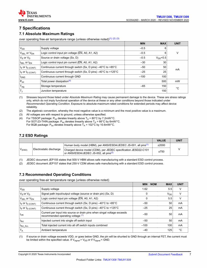
7 Specifications7.1 Absolute Maximum Ratingsover operating free-air temperature range (unless otherwise noted)(1) (2) (3)
MIN MAX UNITVDD Supply voltage –0.5 6
VVSEL or VEN Logic control input pin voltage (EN, A0, A1, A2) –0.5 6
VS or VD Source or drain voltage (Sx, D) –0.5 VDD+0.5
ISEL or IEN Logic control input pin current (EN, A0, A1, A2) –30 30
mAIS or ID (CONT) Continuous current through switch (Sx, D pins) –40°C to +85°C –50 50
IS or ID (CONT) Continuous current through switch (Sx, D pins) –40°C to +125°C –25 25
IGND Continuous current through GND –100 100
Ptot Total power dissipation(4) 500 mW
Tstg Storage temperature –65 150°C
TJ Junction temperature 150
(1) Stresses beyond those listed under Absolute Maximum Rating may cause permanent damage to the device. These are stress ratingsonly, which do not imply functional operation of the device at these or any other conditions beyond those indicated underRecommended Operating Condition. Exposure to absolute-maximum-rated conditions for extended periods may affect devicereliability.
(2) The algebraic convention, whereby the most negative value is a minimum and the most positive value is a maximum.(3) All voltages are with respect to ground, unless otherwise specified.(4) For TSSOP package: Ptot derates linearily above TA = 80°C by 7.2mW/°C.
For SOT-23-THIN package: Ptot derates linearily above TA = 66°C by 6mW/°C.For BQB package: Ptot derates linearily above TA = 102°C by 10.6mW/°C.
7.2 ESD RatingsVALUE UNIT
V(ESD) Electrostatic dischargeHuman body model (HBM), per ANSI/ESDA/JEDEC JS-001, all pins(1) ±2000
VCharged device model (CDM), per JEDEC specification JESD22-C101or ANSI/ESDA/JEDEC JS-002, all pins(2) ±750
(1) JEDEC document JEP155 states that 500-V HBM allows safe manufacturing with a standard ESD control process.(2) JEDEC document JEP157 states that 250-V CDM allows safe manufacturing with a standard ESD control process.
7.3 Recommended Operating Conditionsover operating free-air temperature range (unless otherwise noted)
MIN NOM MAX UNITVDD Supply voltage 1.62 5.5 V
VS or VD Signal path input/output voltage (source or drain pin) (Sx, D) 0 VDD V
VSEL or VEN Logic control input pin voltage (EN, A0, A1, A2) 0 5.5 V
IS or ID (CONT) Continuous current through switch (Sx, D pins) –40°C to +85°C –50 50 mA
IS or ID (CONT) Continuous current through switch (Sx, D pins) –40°C to +125°C –25 25 mA
IOKCurrent per input into source or drain pins when singal voltage exceedsrecommended operating voltage (1) –50 50 mA
IINJ Injected current into single off switch input –50 50 mA
IINJ_ALL Total injected current into all off switch inputs combined –100 100 mA
TA Ambient temperature –40 125 °C
(1) If source or drain voltage exceeds VDD, or goes below GND, the pin will be shunted to GND through an internal FET, the current mustbe limited within the specified value. If Vsignal > VDD or if Vsignal < GND.
www.ti.comTMUX1308, TMUX1309
SCDS426D – MARCH 2020 – REVISED NOVEMBER 2020
Copyright © 2020 Texas Instruments Incorporated Submit Document Feedback 7
Product Folder Links: TMUX1308 TMUX1309
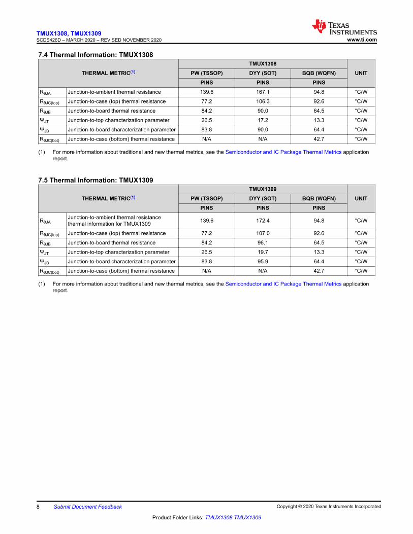
7.4 Thermal Information: TMUX1308
THERMAL METRIC(1)
TMUX1308UNITPW (TSSOP) DYY (SOT) BQB (WQFN)
PINS PINS PINSRθJA Junction-to-ambient thermal resistance 139.6 167.1 94.8 °C/W
RθJC(top) Junction-to-case (top) thermal resistance 77.2 106.3 92.6 °C/W
RθJB Junction-to-board thermal resistance 84.2 90.0 64.5 °C/W
ΨJT Junction-to-top characterization parameter 26.5 17.2 13.3 °C/W
ΨJB Junction-to-board characterization parameter 83.8 90.0 64.4 °C/W
RθJC(bot) Junction-to-case (bottom) thermal resistance N/A N/A 42.7 °C/W
(1) For more information about traditional and new thermal metrics, see the Semiconductor and IC Package Thermal Metrics applicationreport.
7.5 Thermal Information: TMUX1309
THERMAL METRIC(1)
TMUX1309UNITPW (TSSOP) DYY (SOT) BQB (WQFN)
PINS PINS PINS
RθJAJunction-to-ambient thermal resistancethermal information for TMUX1309 139.6 172.4 94.8 °C/W
RθJC(top) Junction-to-case (top) thermal resistance 77.2 107.0 92.6 °C/W
RθJB Junction-to-board thermal resistance 84.2 96.1 64.5 °C/W
ΨJT Junction-to-top characterization parameter 26.5 19.7 13.3 °C/W
ΨJB Junction-to-board characterization parameter 83.8 95.9 64.4 °C/W
RθJC(bot) Junction-to-case (bottom) thermal resistance N/A N/A 42.7 °C/W
(1) For more information about traditional and new thermal metrics, see the Semiconductor and IC Package Thermal Metrics applicationreport.
TMUX1308, TMUX1309SCDS426D – MARCH 2020 – REVISED NOVEMBER 2020 www.ti.com
8 Submit Document Feedback Copyright © 2020 Texas Instruments Incorporated
Product Folder Links: TMUX1308 TMUX1309
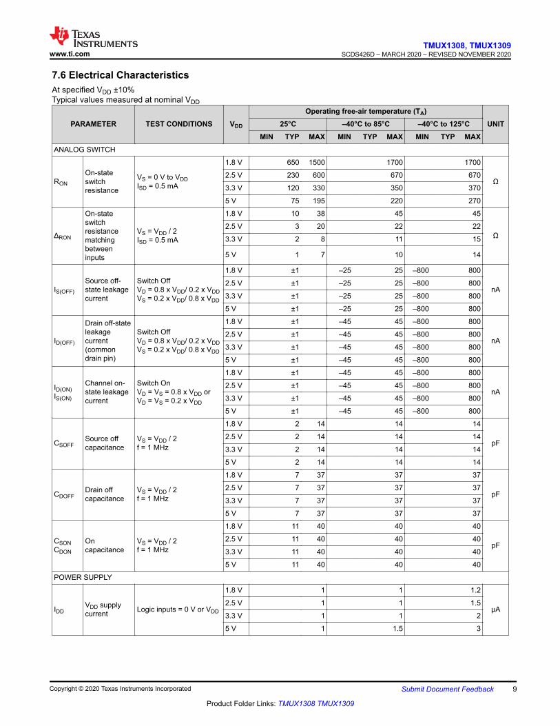
7.6 Electrical CharacteristicsAt specified VDD ±10%Typical values measured at nominal VDD
PARAMETER TEST CONDITIONS VDD
Operating free-air temperature (TA)UNIT25°C –40°C to 85°C –40°C to 125°C
MIN TYP MAX MIN TYP MAX MIN TYP MAXANALOG SWITCH
RON
On-stateswitchresistance
VS = 0 V to VDDISD = 0.5 mA
1.8 V 650 1500 1700 1700
Ω2.5 V 230 600 670 670
3.3 V 120 330 350 370
5 V 75 195 220 270
ΔRON
On-stateswitchresistancematchingbetweeninputs
VS = VDD / 2 ISD = 0.5 mA
1.8 V 10 38 45 45
Ω2.5 V 3 20 22 22
3.3 V 2 8 11 15
5 V 1 7 10 14
IS(OFF)
Source off-state leakagecurrent
Switch OffVD = 0.8 x VDD/ 0.2 x VDDVS = 0.2 x VDD/ 0.8 x VDD
1.8 V ±1 –25 25 –800 800
nA2.5 V ±1 –25 25 –800 800
3.3 V ±1 –25 25 –800 800
5 V ±1 –25 25 –800 800
ID(OFF)
Drain off-stateleakagecurrent(commondrain pin)
Switch OffVD = 0.8 x VDD/ 0.2 x VDDVS = 0.2 x VDD/ 0.8 x VDD
1.8 V ±1 –45 45 –800 800
nA2.5 V ±1 –45 45 –800 800
3.3 V ±1 –45 45 –800 800
5 V ±1 –45 45 –800 800
ID(ON)IS(ON)
Channel on-state leakagecurrent
Switch OnVD = VS = 0.8 x VDD orVD = VS = 0.2 x VDD
1.8 V ±1 –45 45 –800 800
nA2.5 V ±1 –45 45 –800 800
3.3 V ±1 –45 45 –800 800
5 V ±1 –45 45 –800 800
CSOFFSource offcapacitance
VS = VDD / 2f = 1 MHz
1.8 V 2 14 14 14
pF2.5 V 2 14 14 14
3.3 V 2 14 14 14
5 V 2 14 14 14
CDOFFDrain offcapacitance
VS = VDD / 2f = 1 MHz
1.8 V 7 37 37 37
pF2.5 V 7 37 37 37
3.3 V 7 37 37 37
5 V 7 37 37 37
CSONCDON
Oncapacitance
VS = VDD / 2f = 1 MHz
1.8 V 11 40 40 40
pF2.5 V 11 40 40 40
3.3 V 11 40 40 40
5 V 11 40 40 40
POWER SUPPLY
IDDVDD supplycurrent Logic inputs = 0 V or VDD
1.8 V 1 1 1.2
µA2.5 V 1 1 1.5
3.3 V 1 1 2
5 V 1 1.5 3
www.ti.comTMUX1308, TMUX1309
SCDS426D – MARCH 2020 – REVISED NOVEMBER 2020
Copyright © 2020 Texas Instruments Incorporated Submit Document Feedback 9
Product Folder Links: TMUX1308 TMUX1309
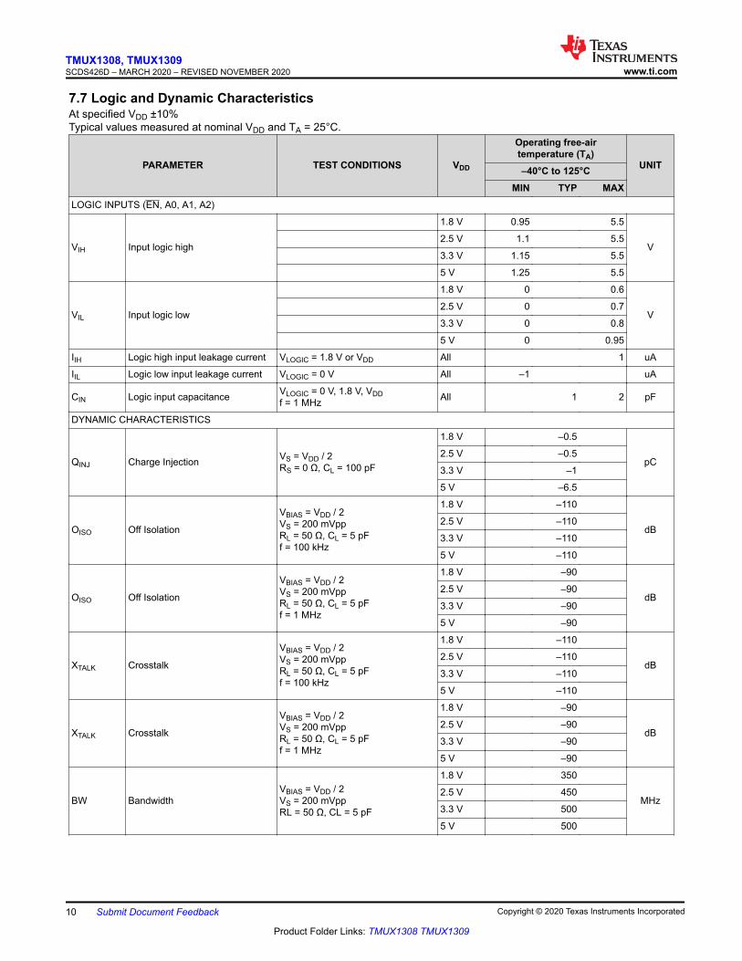
7.7 Logic and Dynamic CharacteristicsAt specified VDD ±10%Typical values measured at nominal VDD and TA = 25°C.
PARAMETER TEST CONDITIONS VDD
Operating free-airtemperature (TA)
UNIT–40°C to 125°CMIN TYP MAX
LOGIC INPUTS (EN, A0, A1, A2)
VIH Input logic high
1.8 V 0.95 5.5
V2.5 V 1.1 5.5
3.3 V 1.15 5.5
5 V 1.25 5.5
VIL Input logic low
1.8 V 0 0.6
V2.5 V 0 0.7
3.3 V 0 0.8
5 V 0 0.95
IIH Logic high input leakage current VLOGIC = 1.8 V or VDD All 1 uA
IIL Logic low input leakage current VLOGIC = 0 V All –1 uA
CIN Logic input capacitance VLOGIC = 0 V, 1.8 V, VDDf = 1 MHz All 1 2 pF
DYNAMIC CHARACTERISTICS
QINJ Charge Injection VS = VDD / 2RS = 0 Ω, CL = 100 pF
1.8 V –0.5
pC2.5 V –0.5
3.3 V –1
5 V –6.5
OISO Off Isolation
VBIAS = VDD / 2VS = 200 mVppRL = 50 Ω, CL = 5 pFf = 100 kHz
1.8 V –110
dB2.5 V –110
3.3 V –110
5 V –110
OISO Off Isolation
VBIAS = VDD / 2VS = 200 mVppRL = 50 Ω, CL = 5 pFf = 1 MHz
1.8 V –90
dB2.5 V –90
3.3 V –90
5 V –90
XTALK Crosstalk
VBIAS = VDD / 2VS = 200 mVppRL = 50 Ω, CL = 5 pFf = 100 kHz
1.8 V –110
dB2.5 V –110
3.3 V –110
5 V –110
XTALK Crosstalk
VBIAS = VDD / 2VS = 200 mVppRL = 50 Ω, CL = 5 pFf = 1 MHz
1.8 V –90
dB2.5 V –90
3.3 V –90
5 V –90
BW BandwidthVBIAS = VDD / 2VS = 200 mVppRL = 50 Ω, CL = 5 pF
1.8 V 350
MHz2.5 V 450
3.3 V 500
5 V 500
TMUX1308, TMUX1309SCDS426D – MARCH 2020 – REVISED NOVEMBER 2020 www.ti.com
10 Submit Document Feedback Copyright © 2020 Texas Instruments Incorporated
Product Folder Links: TMUX1308 TMUX1309
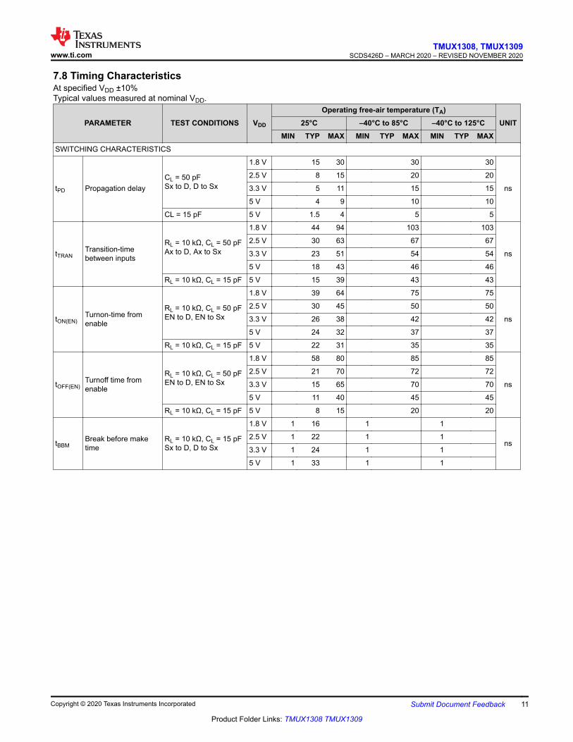
7.8 Timing CharacteristicsAt specified VDD ±10%Typical values measured at nominal VDD.
PARAMETER TEST CONDITIONS VDD
Operating free-air temperature (TA)UNIT25°C –40°C to 85°C –40°C to 125°C
MIN TYP MAX MIN TYP MAX MIN TYP MAXSWITCHING CHARACTERISTICS
tPD Propagation delayCL = 50 pFSx to D, D to Sx
1.8 V 15 30 30 30
ns
2.5 V 8 15 20 20
3.3 V 5 11 15 15
5 V 4 9 10 10
CL = 15 pF 5 V 1.5 4 5 5
tTRANTransition-timebetween inputs
RL = 10 kΩ, CL = 50 pFAx to D, Ax to Sx
1.8 V 44 94 103 103
ns
2.5 V 30 63 67 67
3.3 V 23 51 54 54
5 V 18 43 46 46
RL = 10 kΩ, CL = 15 pF 5 V 15 39 43 43
tON(EN)Turnon-time fromenable
RL = 10 kΩ, CL = 50 pFEN to D, EN to Sx
1.8 V 39 64 75 75
ns
2.5 V 30 45 50 50
3.3 V 26 38 42 42
5 V 24 32 37 37
RL = 10 kΩ, CL = 15 pF 5 V 22 31 35 35
tOFF(EN)Turnoff time fromenable
RL = 10 kΩ, CL = 50 pFEN to D, EN to Sx
1.8 V 58 80 85 85
ns
2.5 V 21 70 72 72
3.3 V 15 65 70 70
5 V 11 40 45 45
RL = 10 kΩ, CL = 15 pF 5 V 8 15 20 20
tBBMBreak before maketime
RL = 10 kΩ, CL = 15 pFSx to D, D to Sx
1.8 V 1 16 1 1
ns2.5 V 1 22 1 1
3.3 V 1 24 1 1
5 V 1 33 1 1
www.ti.comTMUX1308, TMUX1309
SCDS426D – MARCH 2020 – REVISED NOVEMBER 2020
Copyright © 2020 Texas Instruments Incorporated Submit Document Feedback 11
Product Folder Links: TMUX1308 TMUX1309
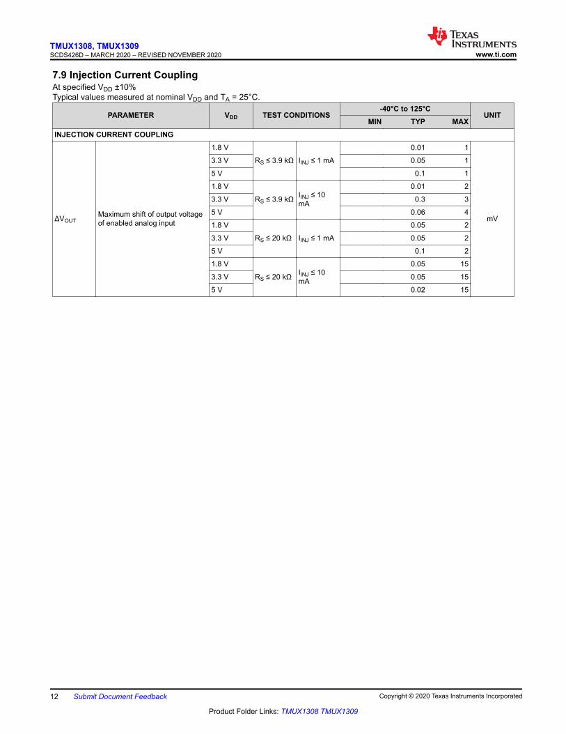
7.9 Injection Current CouplingAt specified VDD ±10%Typical values measured at nominal VDD and TA = 25°C.
PARAMETER VDD TEST CONDITIONS-40°C to 125°C
UNITMIN TYP MAX
INJECTION CURRENT COUPLING
ΔVOUTMaximum shift of output voltageof enabled analog input
1.8 V
RS ≤ 3.9 kΩ IINJ ≤ 1 mA
0.01 1
mV
3.3 V 0.05 1
5 V 0.1 1
1.8 V
RS ≤ 3.9 kΩ IINJ ≤ 10mA
0.01 2
3.3 V 0.3 3
5 V 0.06 4
1.8 V
RS ≤ 20 kΩ IINJ ≤ 1 mA
0.05 2
3.3 V 0.05 2
5 V 0.1 2
1.8 V
RS ≤ 20 kΩ IINJ ≤ 10mA
0.05 15
3.3 V 0.05 15
5 V 0.02 15
TMUX1308, TMUX1309SCDS426D – MARCH 2020 – REVISED NOVEMBER 2020 www.ti.com
12 Submit Document Feedback Copyright © 2020 Texas Instruments Incorporated
Product Folder Links: TMUX1308 TMUX1309
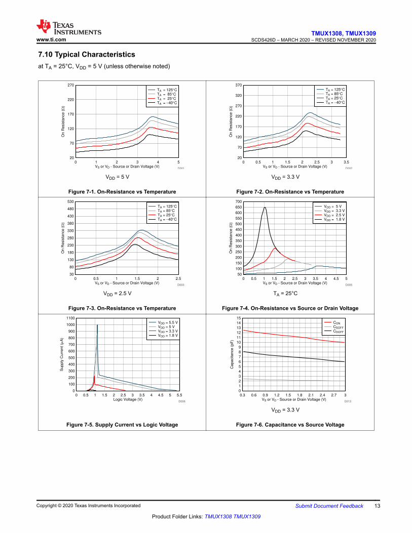
7.10 Typical Characteristicsat TA = 25°C, VDD = 5 V (unless otherwise noted)
VS or VD - Source or Drain Voltage (V)
On
Resis
tan
ce
(:
)
0 1 2 3 4 520
70
120
170
220
270
D001D001
TA = 125qCTA = 85qCTA = 25qCTA = �40qC
VDD = 5 V
Figure 7-1. On-Resistance vs Temperature
VS or VD - Source or Drain Voltage (V)
On
Resis
tan
ce
(:
)
0 0.5 1 1.5 2 2.5 3 3.520
70
120
170
220
270
320
370
D002D002
TA = 125qCTA = 85qCTA = 25qCTA = �40qC
VDD = 3.3 V
Figure 7-2. On-Resistance vs Temperature
VS or VD - Source or Drain Voltage (V)
On
Resis
tan
ce
(:
)
0 0.5 1 1.5 2 2.530
80
130
180
230
280
330
380
430
480
530
D003D003
TA = 125qCTA = 85qCTA = 25qCTA = �40qC
VDD = 2.5 V
Figure 7-3. On-Resistance vs Temperature
VS or VD - Source or Drain Voltage (V)
On
Resis
tan
ce
(:
)
0 0.5 1 1.5 2 2.5 3 3.5 4 4.5 550
100
150
200
250
300
350
400
450
500
550
600
650
700
D005D005
VDD = 5 VVDD = 3.3 VVDD = 2.5 VVDD = 1.8 V
TA = 25°C
Figure 7-4. On-Resistance vs Source or Drain Voltage
Logic Voltage (V)
Su
pp
ly C
urr
en
t (P
A)
0 0.5 1 1.5 2 2.5 3 3.5 4 4.5 5 5.50
100
200
300
400
500
600
700
800
900
1000
1100
D006D006
VDD = 5.5 VVDD = 5 VVDD = 3.3 VVDD = 1.8 V
.
Figure 7-5. Supply Current vs Logic Voltage
VS or VD - Source or Drain Voltage (V)
Ca
pa
cita
nce
(p
F)
0.3 0.6 0.9 1.2 1.5 1.8 2.1 2.4 2.7 30
1
2
3
4
5
6
7
8
9
10
11
12
13
14
15
D013D013
CON
CSOFF
CDOFF
VDD = 3.3 V
Figure 7-6. Capacitance vs Source Voltage
www.ti.comTMUX1308, TMUX1309
SCDS426D – MARCH 2020 – REVISED NOVEMBER 2020
Copyright © 2020 Texas Instruments Incorporated Submit Document Feedback 13
Product Folder Links: TMUX1308 TMUX1309
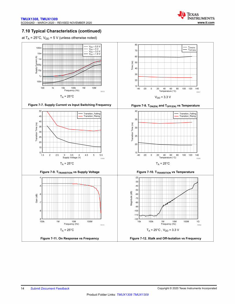
7.10 Typical Characteristics (continued)at TA = 25°C, VDD = 5 V (unless otherwise noted)
Frequency (Hz)
Su
pp
ly C
urr
en
t (A
)
10k 1M 10M
100n
1P
10P
100P
1m
10m
100m
100 1k 100k
D012D012
VDD = 5.5 VVDD = 5 VVDD = 3.3 VVDD = 1.8 V
TA = 25°C
Figure 7-7. Supply Current vs Input Switching Frequency
Temperature (qC)
Tim
e (
ns)
-40 -20 0 20 40 60 80 100 120 14010
20
30
40
50
60
70
80
D007D007
TON(EN)
TOFF(EN)
VDD = 3.3 V
Figure 7-8. TON(EN) and TOFF(EN) vs Temperature
Supply Voltage (V)
Tra
nsitio
n T
ime
(n
s)
1.5 2 2.5 3 3.5 4 4.5 5 5.510
15
20
25
30
35
40
45
50
D008D008
Transiton_FallingTransiton_Rising
TA = 25°C
Figure 7-9. TTRANSITION vs Supply Voltage
Temperature (qC)
Tra
nsitio
n T
ime
(n
s)
-40 -20 0 20 40 60 80 100 120 14015
20
25
30
35
40
D009D009
Transiton_FallingTransiton_Rising
TA = 25°C
Figure 7-10. TTRANSITION vs Temperature
Frequency (Hz)
Ga
in (
dB
)
-9
-8
-7
-6
-5
-4
100k 1M 10M 100M
D010D010
TA = 25°C
Figure 7-11. On Response vs Frequency
Frequency (Hz)
Ma
gn
itu
de
(d
B)
-120
-110
-100
-90
-80
-70
-60
-50
-40
-30
-20
10k 100k 1M 10M 100M 1G
D014D001D014
TA = 25°C , VDD = 3.3 V
Figure 7-12. Xtalk and Off-Isolation vs Frequency
TMUX1308, TMUX1309SCDS426D – MARCH 2020 – REVISED NOVEMBER 2020 www.ti.com
14 Submit Document Feedback Copyright © 2020 Texas Instruments Incorporated
Product Folder Links: TMUX1308 TMUX1309
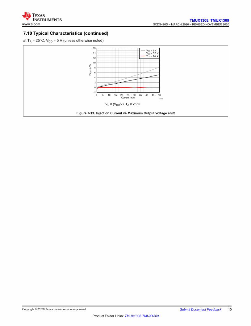
7.10 Typical Characteristics (continued)at TA = 25°C, VDD = 5 V (unless otherwise noted)
Current (mA)
'V
OU
T (P
V)
0 5 10 15 20 25 30 35 40 45 50-2
0
2
4
6
8
10
12
14
16
D011D011
VDD = 5 VVDD = 3.3 VVDD = 1.8 V
VS = (VDD/2), TA = 25°C
Figure 7-13. Injection Current vs Maximum Output Voltage shift
www.ti.comTMUX1308, TMUX1309
SCDS426D – MARCH 2020 – REVISED NOVEMBER 2020
Copyright © 2020 Texas Instruments Incorporated Submit Document Feedback 15
Product Folder Links: TMUX1308 TMUX1309
8 Detailed Description8.1 Overview8.1.1 On-Resistance
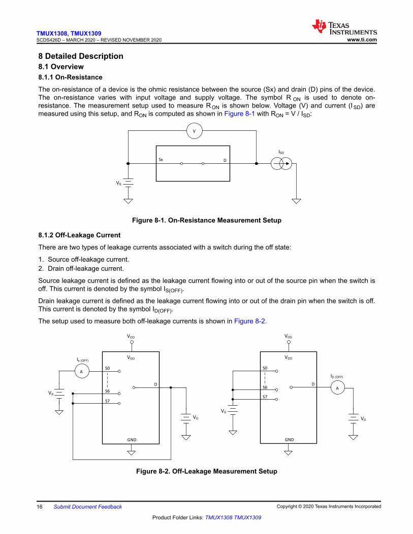
The on-resistance of a device is the ohmic resistance between the source (Sx) and drain (D) pins of the device.The on-resistance varies with input voltage and supply voltage. The symbol R ON is used to denote on-resistance. The measurement setup used to measure R ON is shown below. Voltage (V) and current (I SD) aremeasured using this setup, and RON is computed as shown in Figure 8-1 with RON = V / ISD:
V
D
VS
ISD
Sx
Figure 8-1. On-Resistance Measurement Setup
8.1.2 Off-Leakage Current
There are two types of leakage currents associated with a switch during the off state:
1. Source off-leakage current.2. Drain off-leakage current.
Source leakage current is defined as the leakage current flowing into or out of the source pin when the switch isoff. This current is denoted by the symbol IS(OFF).
Drain leakage current is defined as the leakage current flowing into or out of the drain pin when the switch is off.This current is denoted by the symbol ID(OFF).
The setup used to measure both off-leakage currents is shown in Figure 8-2.
VDD
VDD
S0
GND
VS
S7
D
VD
A
ID (OFF)
VDD
VDD
S0
GND
VS
S7
D
VD
A
Is (OFF)
S6S6
Figure 8-2. Off-Leakage Measurement Setup
TMUX1308, TMUX1309SCDS426D – MARCH 2020 – REVISED NOVEMBER 2020 www.ti.com
16 Submit Document Feedback Copyright © 2020 Texas Instruments Incorporated
Product Folder Links: TMUX1308 TMUX1309

8.1.3 On-Leakage Current
Source on-leakage current is defined as the leakage current flowing into or out of the source pin when the switchis on. This current is denoted by the symbol IS(ON).
Drain on-leakage current is defined as the leakage current flowing into or out of the drain pin when the switch ison. This current is denoted by the symbol ID(ON).
Either the source pin or drain pin is left floating during the measurement. Figure 8-3 shows the circuit used formeasuring the on-leakage current, denoted by IS(ON) or ID(ON).
VDD
VDD
S0
S1
GND
VS
S7
D
VD
ID (ON)
VDD
VDD
S0
S1
GND
VS
S7
D
Vs
A
IS (ON)
N.C.
N.C.A
Figure 8-3. On-Leakage Measurement Setup
8.1.4 Transition Time
Transition time is defined as the time taken by the output of the device to rise or fall 50% after the address signalhas risen or fallen past the 50% threshold. Figure 8-4 shows the setup used to measure transition time, denotedby the symbol tTRANSITION.
VDD
OUTPUT
A0
A1
A2
S0
S1
D
GND
VSEL
S7
VDD
0.1�F
VDD
0 V
tTRAN_HIGH
Output
0 V
tTRAN = max ( tTRAN_HGH, tTRAN_LOW)
VSEL tr < 5ns tf < 5ns
tTRAN_LOW
50% 50%
50% 50%
RL CL
EN
Figure 8-4. Transition-Time Measurement Setup
www.ti.comTMUX1308, TMUX1309
SCDS426D – MARCH 2020 – REVISED NOVEMBER 2020
Copyright © 2020 Texas Instruments Incorporated Submit Document Feedback 17
Product Folder Links: TMUX1308 TMUX1309

8.1.5 Break-Before-Make
Break-before-make delay is a safety feature that prevents two inputs from connecting when the device isswitching. The output first breaks from the on-state switch before making the connection with the next on-stateswitch. The time delay between the break and the make is known as break-before-make delay. Figure 8-5 showsthe setup used to measure break-before-make delay, denoted by the symbol tOPEN(BBM).
VDD
0 V
tBBM_1
90%Output
0 V
tBBM = min ( tBBM_1, tBBM_2)
tBBM_2
Input Select(VSEL)
tr < 5ns tf < 5ns VDD
OUTPUT
A0
A1
A2
S0
S1-S6
D
GND
VSEL
S7
VDD
0.1�F
RL CL
EN
Figure 8-5. Break-Before-Make Delay Measurement Setup
8.1.6 tON(EN) and tOFF(EN)
Turn-on time is defined as the time taken by the output of the device to rise to 10% after the enable has risenpast the 50% threshold. The 10% measurement is utilized to provide the timing of the device, system level timingcan then account for the time constant added from the load resistance and load capacitance. Figure 8-6 showsthe setup used to measure transition time, denoted by the symbol tON(EN).
Turn-off time is defined as the time taken by the output of the device to fall to 90% after the enable has fallenpast the 50% threshold. The 90% measurement is utilized to provide the timing of the device, system level timingcan then account for the time constant added from the load resistance and load capacitance. Figure 8-6 showsthe setup used to measure transition time, denoted by the symbol tOFF(EN).
VDD
0 V
VEN
tON (EN) tOFF (EN)
90%
10%
OUTPUT
0 V
tr < 5nstf < 5ns
VDD
OUTPUT
S0
S1
D
GND
VEN
S7
VDD
0.1�F
RL CL
A0
A1
A2
EN
50% 50%
Figure 8-6. Turn-On and Turn-Off Time Measurement Setup
TMUX1308, TMUX1309SCDS426D – MARCH 2020 – REVISED NOVEMBER 2020 www.ti.com
18 Submit Document Feedback Copyright © 2020 Texas Instruments Incorporated
Product Folder Links: TMUX1308 TMUX1309
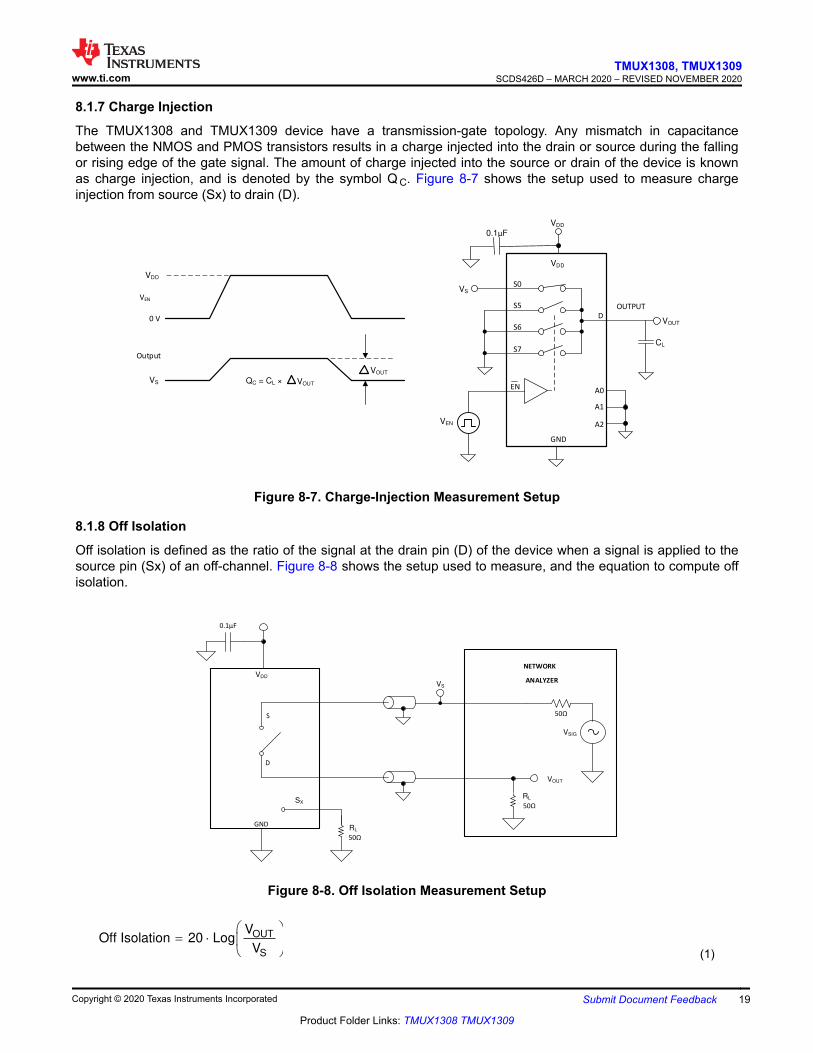
8.1.7 Charge Injection
The TMUX1308 and TMUX1309 device have a transmission-gate topology. Any mismatch in capacitancebetween the NMOS and PMOS transistors results in a charge injected into the drain or source during the fallingor rising edge of the gate signal. The amount of charge injected into the source or drain of the device is knownas charge injection, and is denoted by the symbol Q C. Figure 8-7 shows the setup used to measure chargeinjection from source (Sx) to drain (D).
OUTPUT
CL
GND
VOUT
Output
VS
0 V
VDD
QC = CL × VOUT
VOUT
VEN
VDD
VDD
0.1�F
VS
D
S5
S6
S7
VEN
S0
ENA0
A1
A2
Figure 8-7. Charge-Injection Measurement Setup
8.1.8 Off Isolation
Off isolation is defined as the ratio of the signal at the drain pin (D) of the device when a signal is applied to thesource pin (Sx) of an off-channel. Figure 8-8 shows the setup used to measure, and the equation to compute offisolation.
GND
NETWORK
ANALYZER
VOUT
S
D
50Q�
VSIG
RL
50Q�SX
RL
50Q�
VS
VDD
0.1µF
Figure 8-8. Off Isolation Measurement Setup
OUT
S
VOff Isolation 20 Log
V
§ · � ¨ ¸
© ¹ (1)
www.ti.comTMUX1308, TMUX1309
SCDS426D – MARCH 2020 – REVISED NOVEMBER 2020
Copyright © 2020 Texas Instruments Incorporated Submit Document Feedback 19
Product Folder Links: TMUX1308 TMUX1309
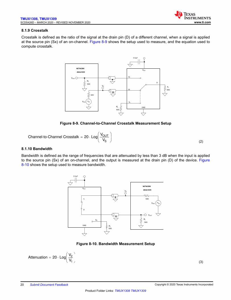
8.1.9 Crosstalk
Crosstalk is defined as the ratio of the signal at the drain pin (D) of a different channel, when a signal is appliedat the source pin (Sx) of an on-channel. Figure 8-9 shows the setup used to measure, and the equation used tocompute crosstalk.
NETWORK
ANALYZER
GND
S1
S2
VSIG
50Q�
VOUT
RL
50Q�
RL
D
SX
50Q�
50Q�
RL
VS
VDD
0.1µF
Figure 8-9. Channel-to-Channel Crosstalk Measurement Setup
OUT
S
VChannel-to-Channel Crosstalk 20 Log
V
§ · � ¨ ¸
© ¹ (2)
8.1.10 Bandwidth
Bandwidth is defined as the range of frequencies that are attenuated by less than 3 dB when the input is appliedto the source pin (Sx) of an on-channel, and the output is measured at the drain pin (D) of the device. Figure8-10 shows the setup used to measure bandwidth.
GND
NETWORK
ANALYZER
VOUT
S
D
50Q�
VSIG
RL
50Q�
VS
VDD
0.1µF
SX
RL
50Q�
Figure 8-10. Bandwidth Measurement Setup
2
1
VAttenuation 20 Log
V
§ · � ¨ ¸
© ¹ (3)
TMUX1308, TMUX1309SCDS426D – MARCH 2020 – REVISED NOVEMBER 2020 www.ti.com
20 Submit Document Feedback Copyright © 2020 Texas Instruments Incorporated
Product Folder Links: TMUX1308 TMUX1309
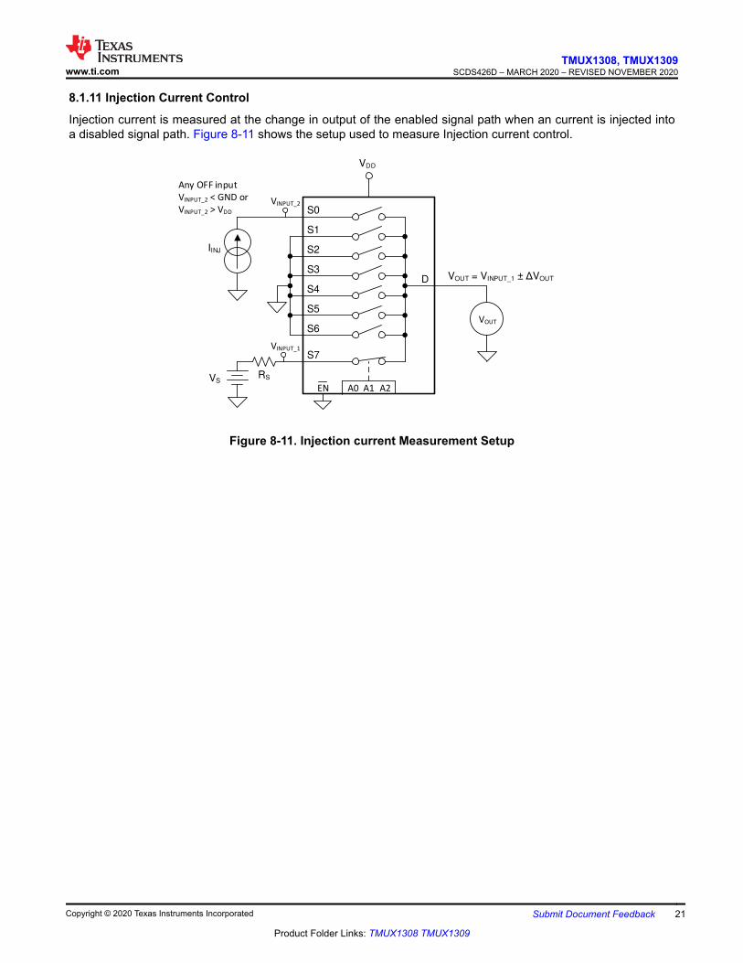
8.1.11 Injection Current Control
Injection current is measured at the change in output of the enabled signal path when an current is injected intoa disabled signal path. Figure 8-11 shows the setup used to measure Injection current control.
VS
IINJ
RS
VDD
S0
S1
S2
S3
S4
S5
S6
S7
VOUT
VOUT = VINPUT_1 ± ûVOUT D
EN A0 A1 A2
Any OFF input
VINPUT_2 < GND or
VINPUT_2 > VDD
VINPUT_2
VINPUT_1
Figure 8-11. Injection current Measurement Setup
www.ti.comTMUX1308, TMUX1309
SCDS426D – MARCH 2020 – REVISED NOVEMBER 2020
Copyright © 2020 Texas Instruments Incorporated Submit Document Feedback 21
Product Folder Links: TMUX1308 TMUX1309

8.2 Functional Block DiagramThe TMUX1308 is an 8:1, single-ended (1-channel), mux. The TMUX1309 is a 4:1, differential (2-channel) mux.Each channel is turned on or turned off based on the state of the address lines and enable pin.
TMUX1308
A0 A1 A2 EN
S1
D
S2
S3
S4
S5
S6
S7
S0
1-OF-8
DECODER
TMUX1309
S0A
DB
S1A
S2A
S3A
S0B
S1B
S2B
S3B
DA
A0 A1 EN
1-OF-4
DECODER
Figure 8-12. TMUX1308 and TMUX1309 Functional Block Diagram
8.3 Feature Description8.3.1 Bidirectional Operation
The TMUX1308 and TMUX1309 devices conduct equally well from source (Sx) to drain (Dx) or from drain (Dx)to source (Sx). Each signal path has very similar characteristics in both directions so they can be used as bothmultiplexers and demultiplexer to supports both analog and digital signals.
8.3.2 Rail-to-Rail Operation
The valid signal path input and output voltage for the TMUX1308 and TMUX1309 ranges from GND to VDD.
8.3.3 1.8 V Logic Compatible Inputs
The TMUX1308 and TMUX1309 support 1.8-V logic compatible control for all logic control inputs. The logic inputthresholds scale with supply but still provide 1.8-V logic control when operating at 5.5-V supply voltage. 1.8-Vlogic level inputs allows the multiplexers to interface with processors that have lower logic I/O rails andeliminates the need for an external voltage translator, which saves both space and BOM cost. The currentconsumption of the TMUX1308 and TMUX1309 devices increase when using 1.8-V logic with higher supplyvoltage. For more information on 1.8-V logic implementations refer to Simplifying Design with 1.8 V logic Muxesand Switches.
8.3.4 Fail-Safe Logic
The TMUX1308 and TMUX1309 device have Fail-Safe Logic on the control input pins (EN, A0, A1, and A2)allowing for operation up to 5.5-V, regardless of the state of the supply pin. This feature allows voltages on thecontrol pins to be applied before the supply pin, protecting the device from potential damage. Fail-Safe Logicminimizes system complexity by removing the need for power supply sequencing on the logic control pins. Forexample, the Fail-Safe Logic feature allows the select pins of the TMUX1308 and TMUX1309 to be ramped to5.5-V while V DD = 0-V. Additionally, the feature enables operation of the multiplexers with V DD = 1.8-V whileallowing the select pins to interface with a logic level of another device up to 5.5-V, eliminating the potential needfor an external voltage translator.
8.3.5 Injection Current Control
Injection current is the current that is being forced into a pin by an input voltage (V IN) higher than the positivesupply (V DD + ∆V) or lower than ground (V SS). The current flows through the input protection diodes intowhichever supply of the device potentially compromising the accuracy and reliability of the system. Injectedcurrents can come from various sources depending on the application.
TMUX1308, TMUX1309SCDS426D – MARCH 2020 – REVISED NOVEMBER 2020 www.ti.com
22 Submit Document Feedback Copyright © 2020 Texas Instruments Incorporated
Product Folder Links: TMUX1308 TMUX1309
• Harsh environments and applications with long cabling, such as in factory automation and automotivesystems, may be susceptible to injected currents from switching or transient events.
• Other self-contained systems can also be subject to injected current if the input signal is coming from varioussensors or current sources.
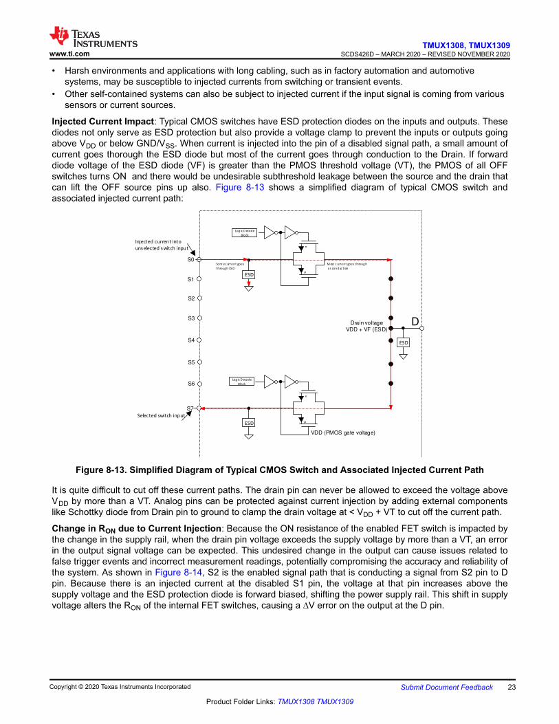
Injected Current Impact: Typical CMOS switches have ESD protection diodes on the inputs and outputs. Thesediodes not only serve as ESD protection but also provide a voltage clamp to prevent the inputs or outputs goingabove VDD or below GND/VSS. When current is injected into the pin of a disabled signal path, a small amount ofcurrent goes thorough the ESD diode but most of the current goes through conduction to the Drain. If forwarddiode voltage of the ESD diode (VF) is greater than the PMOS threshold voltage (VT), the PMOS of all OFFswitches turns ON and there would be undesirable subthreshold leakage between the source and the drain thatcan lift the OFF source pins up also. Figure 8-13 shows a simplified diagram of typical CMOS switch andassociated injected current path:
S0
Injected current into
unselected switch input
S7
Som e c urrent goes
throug h ES D
Drain voltage
VDD + VF (ESD)
M ost c urrent goes throug h
a s conduc ti on
VDD (PMOS gate voltage)
Selected switch input
ESD
S1
S2
S3
S4
S5
S6
D
ESD
n
p
Log ic D ecode
Block
n
p
ESD
Log ic D ecode
Block
Figure 8-13. Simplified Diagram of Typical CMOS Switch and Associated Injected Current Path
It is quite difficult to cut off these current paths. The drain pin can never be allowed to exceed the voltage aboveVDD by more than a VT. Analog pins can be protected against current injection by adding external componentslike Schottky diode from Drain pin to ground to clamp the drain voltage at < VDD + VT to cut off the current path.
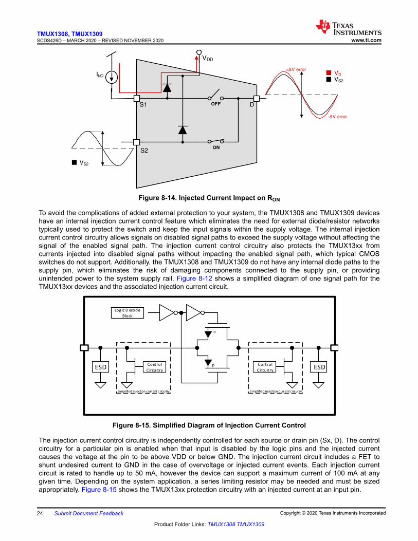
Change in RON due to Current Injection: Because the ON resistance of the enabled FET switch is impacted bythe change in the supply rail, when the drain pin voltage exceeds the supply voltage by more than a VT, an errorin the output signal voltage can be expected. This undesired change in the output can cause issues related tofalse trigger events and incorrect measurement readings, potentially compromising the accuracy and reliability ofthe system. As shown in Figure 8-14, S2 is the enabled signal path that is conducting a signal from S2 pin to Dpin. Because there is an injected current at the disabled S1 pin, the voltage at that pin increases above thesupply voltage and the ESD protection diode is forward biased, shifting the power supply rail. This shift in supplyvoltage alters the RON of the internal FET switches, causing a ∆V error on the output at the D pin.
www.ti.comTMUX1308, TMUX1309
SCDS426D – MARCH 2020 – REVISED NOVEMBER 2020
Copyright © 2020 Texas Instruments Incorporated Submit Document Feedback 23
Product Folder Links: TMUX1308 TMUX1309
S1
S2
II/O
D
VDD
-ûV error
ON
OFF
+ûV error
VS2
VD
VS2
Figure 8-14. Injected Current Impact on RON
To avoid the complications of added external protection to your system, the TMUX1308 and TMUX1309 deviceshave an internal injection current control feature which eliminates the need for external diode/resistor networkstypically used to protect the switch and keep the input signals within the supply voltage. The internal injectioncurrent control circuitry allows signals on disabled signal paths to exceed the supply voltage without affecting thesignal of the enabled signal path. The injection current control circuitry also protects the TMUX13xx fromcurrents injected into disabled signal paths without impacting the enabled signal path, which typical CMOSswitches do not support. Additionally, the TMUX1308 and TMUX1309 do not have any internal diode paths to thesupply pin, which eliminates the risk of damaging components connected to the supply pin, or providingunintended power to the system supply rail. Figure 8-12 shows a simplified diagram of one signal path for theTMUX13xx devices and the associated injection current circuit.
ESD
n
pControl
Circuitry
Simplified injection curr ent circuitry
Log ic D ecode
Block
ESDControl
Circuitry
Simplified injection curr ent circuitry
Figure 8-15. Simplified Diagram of Injection Current Control
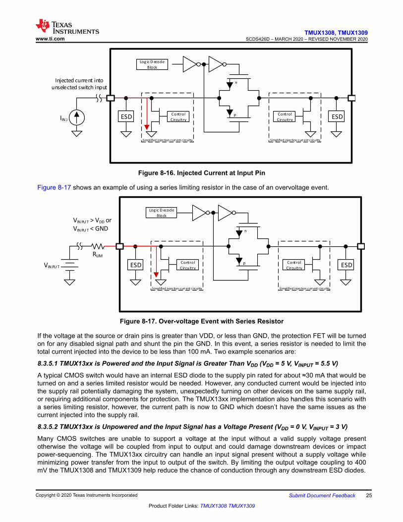
The injection current control circuitry is independently controlled for each source or drain pin (Sx, D). The controlcircuitry for a particular pin is enabled when that input is disabled by the logic pins and the injected currentcauses the voltage at the pin to be above VDD or below GND. The injection current circuit includes a FET toshunt undesired current to GND in the case of overvoltage or injected current events. Each injection currentcircuit is rated to handle up to 50 mA, however the device can support a maximum current of 100 mA at anygiven time. Depending on the system application, a series limiting resistor may be needed and must be sizedappropriately. Figure 8-15 shows the TMUX13xx protection circuitry with an injected current at an input pin.
TMUX1308, TMUX1309SCDS426D – MARCH 2020 – REVISED NOVEMBER 2020 www.ti.com
24 Submit Document Feedback Copyright © 2020 Texas Instruments Incorporated
Product Folder Links: TMUX1308 TMUX1309
ESD
n
pControl
Circuitry
Simplified injection curr ent circuitry
Log ic D ecode
Block
ESDControl
Circuitry
Simplified injection curr ent circuitry
Injected current into
unselected switch input
IIN J
Figure 8-16. Injected Current at Input Pin
Figure 8-17 shows an example of using a series limiting resistor in the case of an overvoltage event.
RLIM
ESD
n
pControl
Circuitry
Simplified injection curr ent circuitry
Log ic D ecode
Block
ESDControl
Circuitry
Simplified injection curr ent circuitry
VIN PU T > VDD or
VIN PU T < GND
VIN PU T
Figure 8-17. Over-voltage Event with Series Resistor
If the voltage at the source or drain pins is greater than VDD, or less than GND, the protection FET will be turnedon for any disabled signal path and shunt the pin the GND. In this event, a series resistor is needed to limit thetotal current injected into the device to be less than 100 mA. Two example scenarios are:
8.3.5.1 TMUX13xx is Powered and the Input Signal is Greater Than VDD (VDD = 5 V, VINPUT = 5.5 V)
A typical CMOS switch would have an internal ESD diode to the supply pin rated for about ≈30 mA that would beturned on and a series limited resistor would be needed. However, any conducted current would be injected intothe supply rail potentially damaging the system, unexpectedly turning on other devices on the same supply rail,or requiring additional components for protection. The TMUX13xx implementation also handles this scenario witha series limiting resistor, however, the current path is now to GND which doesn’t have the same issues as thecurrent injected into the supply rail.
8.3.5.2 TMUX13xx is Unpowered and the Input Signal has a Voltage Present (VDD = 0 V, VINPUT = 3 V)
Many CMOS switches are unable to support a voltage at the input without a valid supply voltage presentotherwise the voltage will be coupled from input to output and could damage downstream devices or impactpower-sequencing. The TMUX13xx circuitry can handle an input signal present without a supply voltage whileminimizing power transfer from the input to output of the switch. By limiting the output voltage coupling to 400mV the TMUX1308 and TMUX1309 help reduce the chance of conduction through any downstream ESD diodes.
www.ti.comTMUX1308, TMUX1309
SCDS426D – MARCH 2020 – REVISED NOVEMBER 2020
Copyright © 2020 Texas Instruments Incorporated Submit Document Feedback 25
Product Folder Links: TMUX1308 TMUX1309
8.3.6 Device Functional Modes
When the EN pin of the TMUX1308 is pulled low, one of the switches is closed based on the state of the addresslines. Similarly, when the EN pin of the TMUX1309 is pulled low, two of the switches are closed based on thestate of the address lines. When the EN pin is pulled high, all the switches are in an open state regardless of thestate of the address lines.
Unused logic control pins must be tied to GND or VDD in order to ensure the device does not consume additionalcurrent as highlighted in Implications of Slow or Floating CMOS Inputs. Unused signal path inputs (Sx and Dx)should be connected to GND.
8.3.7 Truth Tables
Table 8-1 and Table 8-2 show the truth tables for the TMUX1308 and TMUX1309 respectively.
Table 8-1. TMUX1308 Truth TableEN A2 A1 A0 Selected Signal Path Connected To Drain
(D) Pin0 0 0 0 S0
0 0 0 1 S1
0 0 1 0 S2
0 0 1 1 S3
0 1 0 0 S4
0 1 0 1 S5
0 1 1 0 S6
0 1 1 1 S7
1 X(1) X(1) X(1) All channels are off
(1) X denotes don't care.
Table 8-2. TMUX1309 Truth TableEN A1 A0 Selected Signal Path Connected To Drain (DA
and DB) Pins
0 0 0 S0A to DAS0B to DB
0 0 1 S1A to DAS1B to DB
0 1 0 S2A to DAS2B to DB
0 1 1 S3A to DAS3B to DB
1 X(1) X(1) All channels are off
(1) X denotes don't care.
TMUX1308, TMUX1309SCDS426D – MARCH 2020 – REVISED NOVEMBER 2020 www.ti.com
26 Submit Document Feedback Copyright © 2020 Texas Instruments Incorporated
Product Folder Links: TMUX1308 TMUX1309
9 Application and ImplementationNote
Information in the following applications sections is not part of the TI component specification, and TIdoes not warrant its accuracy or completeness. TI’s customers are responsible for determiningsuitability of components for their purposes. Customers should validate and test their designimplementation to confirm system functionality.
9.1 Application InformationThe TMUX13xx family offers protection against injection current invents across a wide operating supply range(1.62 V to 5.5 V). These devices include 1.8 V logic compatible control input pins that enable operation insystems with 1.8 V I/O rails. Additionally, the control input pins support Fail-Safe Logic which allows for operationup to 5.5 V, regardless of the state of the supply pin. This feature stops the logic pins from back-powering thesupply rail while the injection current circuitry prevents the signal path from back-powering the supply. Thesefeatures make the TMUX13xx a family of general purpose multiplexers and switches that can reduce systemcomplexity, board size, and overall system cost.
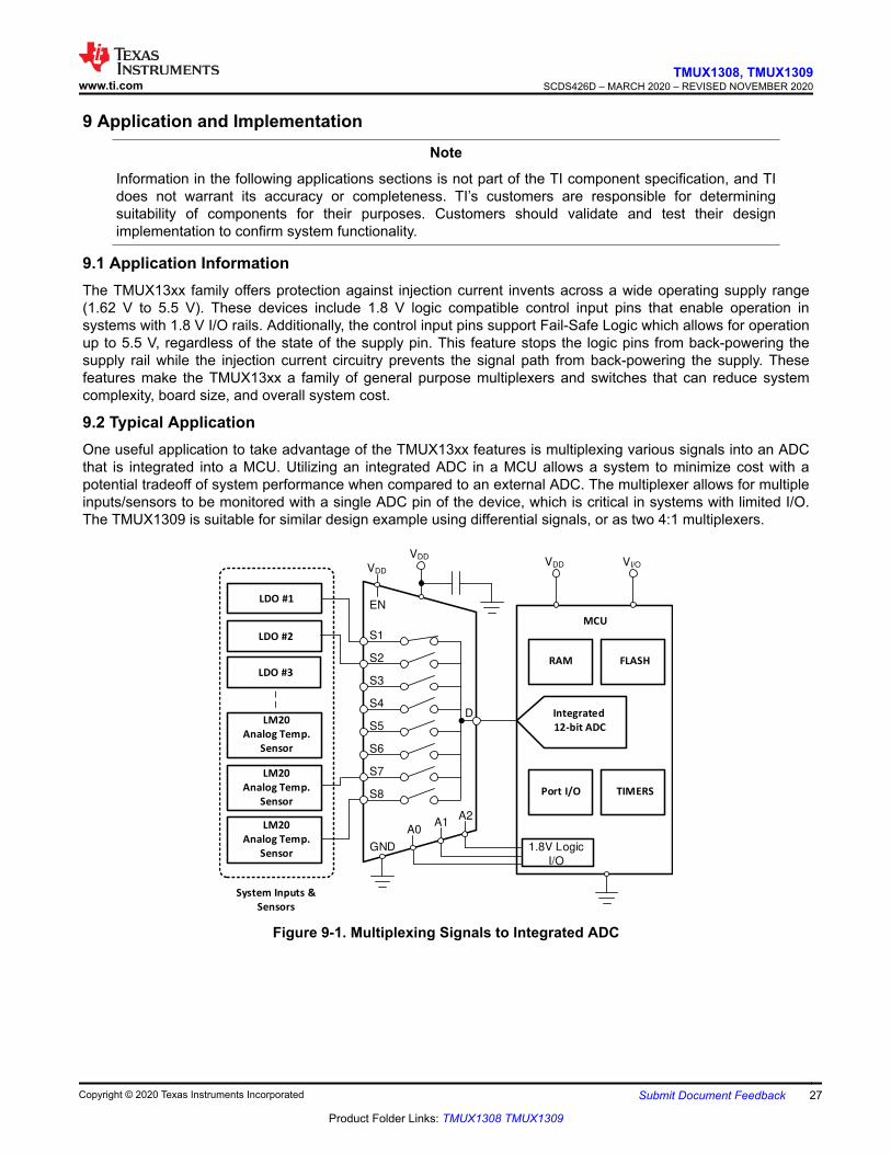
9.2 Typical ApplicationOne useful application to take advantage of the TMUX13xx features is multiplexing various signals into an ADCthat is integrated into a MCU. Utilizing an integrated ADC in a MCU allows a system to minimize cost with apotential tradeoff of system performance when compared to an external ADC. The multiplexer allows for multipleinputs/sensors to be monitored with a single ADC pin of the device, which is critical in systems with limited I/O.The TMUX1309 is suitable for similar design example using differential signals, or as two 4:1 multiplexers.
System Inputs &
Sensors
LDO #1
D
S1
S2
S3
S4
S5
S6
S7
S8
Integrated
12-bit ADC
A0A1
A2
EN
MCU
LDO #2
LM20
Analog Temp.
Sensor
LM20
Analog Temp.
SensorGND
VDD
VDDVDD VI/O
1.8V Logic
I/O
LM20
Analog Temp.
Sensor
LDO #3RAM FLASH
Port I/O TIMERS
Figure 9-1. Multiplexing Signals to Integrated ADC
www.ti.comTMUX1308, TMUX1309
SCDS426D – MARCH 2020 – REVISED NOVEMBER 2020
Copyright © 2020 Texas Instruments Incorporated Submit Document Feedback 27
Product Folder Links: TMUX1308 TMUX1309
9.3 Design RequirementsFor this design example, use the parameters listed in Table 9-1.
Table 9-1. Design ParametersPARAMETERS VALUES
Supply (VDD) 5.0 V
I/O signal range 0 V to VDD (Rail to Rail)
Control logic thresholds 1.8 V compatible
9.4 Detailed Design ProcedureThe TMUX1308 and TMUX1309 can be operated without any external components except for the supplydecoupling capacitors. If the parts desired power-up state is disabled, the enable pin should have a weak pull-upresistor and be controlled by the MCU through the GPIO. All inputs being muxed to the ADC of the MCU mustfall within the recommend operating conditions of the TMUX1308 and TMUX1309 including signal range andcontinuous current. For this design with a supply of 5 V, the signal range can be 0 V to 5 V; the max continuouscurrent can be 100 mA at an ambient temperature of 85°C or 25 mA at 125°C.
10 Power Supply RecommendationsThe TMUX1308 and TMUX1309 devices operate across a wide supply range of 1.62 V to 5.5 V. Note: do notexceed the absolute maximum ratings because stresses beyond the listed ratings can cause permanent damageto the devices.
Power-supply bypassing improves noise margin and prevents switching noise propagation from the VDD supplyto other components. Good power-supply decoupling is important to achieve optimum performance. Forimproved supply noise immunity, use a supply decoupling capacitor ranging from 0.1 μF to 10 μF from VDD toground. Place the bypass capacitors as close to the power supply pins of the device as possible using low-impedance connections. TI recommends using multi-layer ceramic chip capacitors (MLCCs) that offer lowequivalent series resistance (ESR) and inductance (ESL) characteristics for power-supply decoupling purposes.For very sensitive systems, or for systems in harsh noise environments, avoiding the use of vias for connectingthe capacitors to the device pins may offer superior noise immunity. The use of multiple vias in parallel lowersthe overall inductance and is beneficial for connections to ground planes.
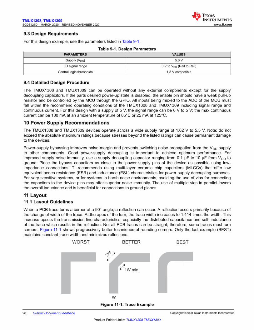
11 Layout11.1 Layout GuidelinesWhen a PCB trace turns a corner at a 90° angle, a reflection can occur. A reflection occurs primarily because ofthe change of width of the trace. At the apex of the turn, the trace width increases to 1.414 times the width. Thisincrease upsets the transmission-line characteristics, especially the distributed capacitance and self–inductanceof the trace which results in the reflection. Not all PCB traces can be straight; therefore, some traces must turncorners. Figure 11-1 shows progressively better techniques of rounding corners. Only the last example (BEST)maintains constant trace width and minimizes reflections.
WORST BETTER BEST
1W min.
W
2W
Figure 11-1. Trace Example
TMUX1308, TMUX1309SCDS426D – MARCH 2020 – REVISED NOVEMBER 2020 www.ti.com
28 Submit Document Feedback Copyright © 2020 Texas Instruments Incorporated
Product Folder Links: TMUX1308 TMUX1309

Route high-speed signals using a minimum of vias and corners which reduces signal reflections and impedancechanges. When a via must be used, increase the clearance size around it to minimize its capacitance. Each viaintroduces discontinuities in the signal’s transmission line and increases the chance of picking up interferencefrom the other layers of the board. Be careful when designing test points, through-hole pins are notrecommended at high frequencies.
Figure 11-2 illustrates an example of a PCB layout with the TMUX1308 and TMUX1309. Some keyconsiderations are:
• Decouple the VDD pin with a 0.1-µF capacitor, placed as close to the pin as possible. Make sure that thecapacitor voltage rating is sufficient for the VDD supply.
• Keep the input lines as short as possible.• Use a solid ground plane to help reduce electromagnetic interference (EMI) noise pickup.• Do not run sensitive analog traces in parallel with digital traces. Avoid crossing digital and analog traces if
possible, and only make perpendicular crossings when necessary.
11.2 Layout Example
N.C.
GND
A1
A2
S4
S6
D
S7
S5
EN
VDD
S2
S1
S0
S3
A0
TMUX1308
Via to GND plane
C
Wide (low inductance)
trace for power
N.C.
GND
A0
A1
S0B
S2B
DB
S3B
S1B
EN
VDD
S2A
S1A
DA
S0A
S3A
TMUX1309
C
Wide (low inductance)
trace for power
Figure 11-2. TMUX1308 and TMUX1309 Layout Example
www.ti.comTMUX1308, TMUX1309
SCDS426D – MARCH 2020 – REVISED NOVEMBER 2020
Copyright © 2020 Texas Instruments Incorporated Submit Document Feedback 29
Product Folder Links: TMUX1308 TMUX1309
12 Device and Documentation Support12.1 Documentation Support12.1.1 Related Documentation
Texas Instruments, Simplifying Design with 1.8 V logic Muxes and Switches.
Texas Instruments, QFN/SON PCB Attachment.
Texas Instruments, Quad Flatpack No-Lead Logic Packages.
12.2 Related LinksThe table below lists quick access links. Categories include technical documents, support and communityresources, tools and software, and quick access to order now.
Table 12-1. Related LinksPARTS PRODUCT FOLDER ORDER NOW TECHNICAL
DOCUMENTSTOOLS &
SOFTWARESUPPORT &COMMUNITY
TMUX1308 Click here Click here Click here Click here Click here
TMUX1309 Click here Click here Click here Click here Click here
12.3 Receiving Notification of Documentation UpdatesTo receive notification of documentation updates, navigate to the device product folder on ti.com. In the upperright corner, click on Alert me to register and receive a weekly digest of any product information that haschanged. For change details, review the revision history included in any revised document.
12.4 Support ResourcesTI E2E™ support forums are an engineer's go-to source for fast, verified answers and design help — straightfrom the experts. Search existing answers or ask your own question to get the quick design help you need.
Linked content is provided "AS IS" by the respective contributors. They do not constitute TI specifications and donot necessarily reflect TI's views; see TI's Terms of Use.
12.5 TrademarksTI E2E™ is a trademark of Texas Instruments.All trademarks are the property of their respective owners.12.6 Electrostatic Discharge Caution
This integrated circuit can be damaged by ESD. Texas Instruments recommends that all integrated circuits be handledwith appropriate precautions. Failure to observe proper handling and installation procedures can cause damage.ESD damage can range from subtle performance degradation to complete device failure. Precision integrated circuits maybe more susceptible to damage because very small parametric changes could cause the device not to meet its publishedspecifications.
12.7 GlossaryTI Glossary This glossary lists and explains terms, acronyms, and definitions.
TMUX1308, TMUX1309SCDS426D – MARCH 2020 – REVISED NOVEMBER 2020 www.ti.com
30 Submit Document Feedback Copyright © 2020 Texas Instruments Incorporated
Product Folder Links: TMUX1308 TMUX1309
13 Mechanical, Packaging, and Orderable InformationThe following pages include mechanical, packaging, and orderable information. This information is the mostcurrent data available for the designated devices. This data is subject to change without notice and revision ofthis document. For browser-based versions of this data sheet, refer to the left-hand navigation.
www.ti.comTMUX1308, TMUX1309
SCDS426D – MARCH 2020 – REVISED NOVEMBER 2020
Copyright © 2020 Texas Instruments Incorporated Submit Document Feedback 31
Product Folder Links: TMUX1308 TMUX1309

PACKAGE OPTION ADDENDUM
www.ti.com 4-Oct-2021
Addendum-Page 1
PACKAGING INFORMATION
Orderable Device Status(1)
Package Type PackageDrawing
Pins PackageQty
Eco Plan(2)
Lead finish/Ball material
(6)
MSL Peak Temp(3)
Op Temp (°C) Device Marking(4/5)
Samples
TMUX1308BQBR ACTIVE WQFN BQB 16 3000 RoHS & Green NIPDAU Level-1-260C-UNLIM -40 to 125 1308
TMUX1308DYYR ACTIVE SOT-23-THIN DYY 16 3000 RoHS & Green NIPDAU Level-1-260C-UNLIM -40 to 125 TMUX1308
TMUX1308PWR ACTIVE TSSOP PW 16 2000 RoHS & Green NIPDAU Level-1-260C-UNLIM -40 to 125 TM1308
TMUX1309BQBR ACTIVE WQFN BQB 16 3000 RoHS & Green NIPDAU Level-1-260C-UNLIM -40 to 125 1309
TMUX1309DYYR ACTIVE SOT-23-THIN DYY 16 3000 RoHS & Green NIPDAU Level-1-260C-UNLIM -40 to 125 TMUX1309
TMUX1309PWR ACTIVE TSSOP PW 16 2000 RoHS & Green NIPDAU Level-1-260C-UNLIM -40 to 125 TM1309
(1) The marketing status values are defined as follows:ACTIVE: Product device recommended for new designs.LIFEBUY: TI has announced that the device will be discontinued, and a lifetime-buy period is in effect.NRND: Not recommended for new designs. Device is in production to support existing customers, but TI does not recommend using this part in a new design.PREVIEW: Device has been announced but is not in production. Samples may or may not be available.OBSOLETE: TI has discontinued the production of the device.
(2) RoHS: TI defines "RoHS" to mean semiconductor products that are compliant with the current EU RoHS requirements for all 10 RoHS substances, including the requirement that RoHS substancedo not exceed 0.1% by weight in homogeneous materials. Where designed to be soldered at high temperatures, "RoHS" products are suitable for use in specified lead-free processes. TI mayreference these types of products as "Pb-Free".RoHS Exempt: TI defines "RoHS Exempt" to mean products that contain lead but are compliant with EU RoHS pursuant to a specific EU RoHS exemption.Green: TI defines "Green" to mean the content of Chlorine (Cl) and Bromine (Br) based flame retardants meet JS709B low halogen requirements of <=1000ppm threshold. Antimony trioxide basedflame retardants must also meet the <=1000ppm threshold requirement.
(3) MSL, Peak Temp. - The Moisture Sensitivity Level rating according to the JEDEC industry standard classifications, and peak solder temperature.
(4) There may be additional marking, which relates to the logo, the lot trace code information, or the environmental category on the device.
(5) Multiple Device Markings will be inside parentheses. Only one Device Marking contained in parentheses and separated by a "~" will appear on a device. If a line is indented then it is a continuationof the previous line and the two combined represent the entire Device Marking for that device.
(6) Lead finish/Ball material - Orderable Devices may have multiple material finish options. Finish options are separated by a vertical ruled line. Lead finish/Ball material values may wrap to twolines if the finish value exceeds the maximum column width.
PACKAGE OPTION ADDENDUM
www.ti.com 4-Oct-2021
Addendum-Page 2
Important Information and Disclaimer:The information provided on this page represents TI's knowledge and belief as of the date that it is provided. TI bases its knowledge and belief on informationprovided by third parties, and makes no representation or warranty as to the accuracy of such information. Efforts are underway to better integrate information from third parties. TI has taken andcontinues to take reasonable steps to provide representative and accurate information but may not have conducted destructive testing or chemical analysis on incoming materials and chemicals.TI and TI suppliers consider certain information to be proprietary, and thus CAS numbers and other limited information may not be available for release.
In no event shall TI's liability arising out of such information exceed the total purchase price of the TI part(s) at issue in this document sold by TI to Customer on an annual basis.
OTHER QUALIFIED VERSIONS OF TMUX1308, TMUX1309 :
• Automotive : TMUX1308-Q1, TMUX1309-Q1
NOTE: Qualified Version Definitions:
• Automotive - Q100 devices qualified for high-reliability automotive applications targeting zero defects

PACKAGE MATERIALS INFORMATION
www.ti.com 14-Jun-2022
TAPE AND REEL INFORMATION
Reel Width (W1)
REEL DIMENSIONS
A0B0K0W
Dimension designed to accommodate the component lengthDimension designed to accommodate the component thicknessOverall width of the carrier tapePitch between successive cavity centers
Dimension designed to accommodate the component width
TAPE DIMENSIONS
K0 P1
B0 W
A0Cavity
QUADRANT ASSIGNMENTS FOR PIN 1 ORIENTATION IN TAPE
Pocket Quadrants
Sprocket Holes
Q1 Q1Q2 Q2
Q3 Q3Q4 Q4 User Direction of Feed
P1
ReelDiameter
*All dimensions are nominal
Device PackageType
PackageDrawing
Pins SPQ ReelDiameter
(mm)
ReelWidth
W1 (mm)
A0(mm)
B0(mm)
K0(mm)
P1(mm)
W(mm)
Pin1Quadrant
TMUX1308BQBR WQFN BQB 16 3000 180.0 12.4 2.8 3.8 1.2 4.0 12.0 Q1
TMUX1308DYYR SOT-23-THIN
DYY 16 3000 330.0 12.4 4.8 3.6 1.6 8.0 12.0 Q3
TMUX1308PWR TSSOP PW 16 2000 330.0 12.4 6.9 5.6 1.6 8.0 12.0 Q1
TMUX1309BQBR WQFN BQB 16 3000 180.0 12.4 2.8 3.8 1.2 4.0 12.0 Q1
TMUX1309DYYR SOT-23-THIN
DYY 16 3000 330.0 12.4 4.8 3.6 1.6 8.0 12.0 Q3
TMUX1309PWR TSSOP PW 16 2000 330.0 12.4 6.9 5.6 1.6 8.0 12.0 Q1
Pack Materials-Page 1
PACKAGE MATERIALS INFORMATION
www.ti.com 14-Jun-2022
TAPE AND REEL BOX DIMENSIONS
Width (mm)
W L
H
*All dimensions are nominal
Device Package Type Package Drawing Pins SPQ Length (mm) Width (mm) Height (mm)
TMUX1308BQBR WQFN BQB 16 3000 210.0 185.0 35.0
TMUX1308DYYR SOT-23-THIN DYY 16 3000 336.6 336.6 31.8
TMUX1308PWR TSSOP PW 16 2000 356.0 356.0 35.0
TMUX1309BQBR WQFN BQB 16 3000 210.0 185.0 35.0
TMUX1309DYYR SOT-23-THIN DYY 16 3000 336.6 336.6 31.8
TMUX1309PWR TSSOP PW 16 2000 356.0 356.0 35.0
Pack Materials-Page 2
www.ti.com
PACKAGE OUTLINE
C
14X 0.65
2X4.55
16X 0.300.19
TYP6.66.2
1.2 MAX
0.150.05
0.25GAGE PLANE
-80
BNOTE 4
4.54.3
A
NOTE 3
5.14.9
0.750.50
(0.15) TYP
TSSOP - 1.2 mm max heightPW0016ASMALL OUTLINE PACKAGE
4220204/A 02/2017
1
89
16
0.1 C A B
PIN 1 INDEX AREA
SEE DETAIL A
0.1 C
NOTES: 1. All linear dimensions are in millimeters. Any dimensions in parenthesis are for reference only. Dimensioning and tolerancing per ASME Y14.5M. 2. This drawing is subject to change without notice. 3. This dimension does not include mold flash, protrusions, or gate burrs. Mold flash, protrusions, or gate burrs shall not exceed 0.15 mm per side. 4. This dimension does not include interlead flash. Interlead flash shall not exceed 0.25 mm per side.5. Reference JEDEC registration MO-153.
SEATINGPLANE
A 20DETAIL ATYPICAL
SCALE 2.500
www.ti.com
EXAMPLE BOARD LAYOUT
0.05 MAXALL AROUND
0.05 MINALL AROUND
16X (1.5)
16X (0.45)
14X (0.65)
(5.8)
(R0.05) TYP
TSSOP - 1.2 mm max heightPW0016ASMALL OUTLINE PACKAGE
4220204/A 02/2017
NOTES: (continued) 6. Publication IPC-7351 may have alternate designs. 7. Solder mask tolerances between and around signal pads can vary based on board fabrication site.
LAND PATTERN EXAMPLEEXPOSED METAL SHOWN
SCALE: 10X
SYMM
SYMM
1
8 9
16
15.000
METALSOLDER MASKOPENING
METAL UNDERSOLDER MASK
SOLDER MASKOPENING
EXPOSED METALEXPOSED METAL
SOLDER MASK DETAILS
NON-SOLDER MASKDEFINED
(PREFERRED)
SOLDER MASKDEFINED
www.ti.com
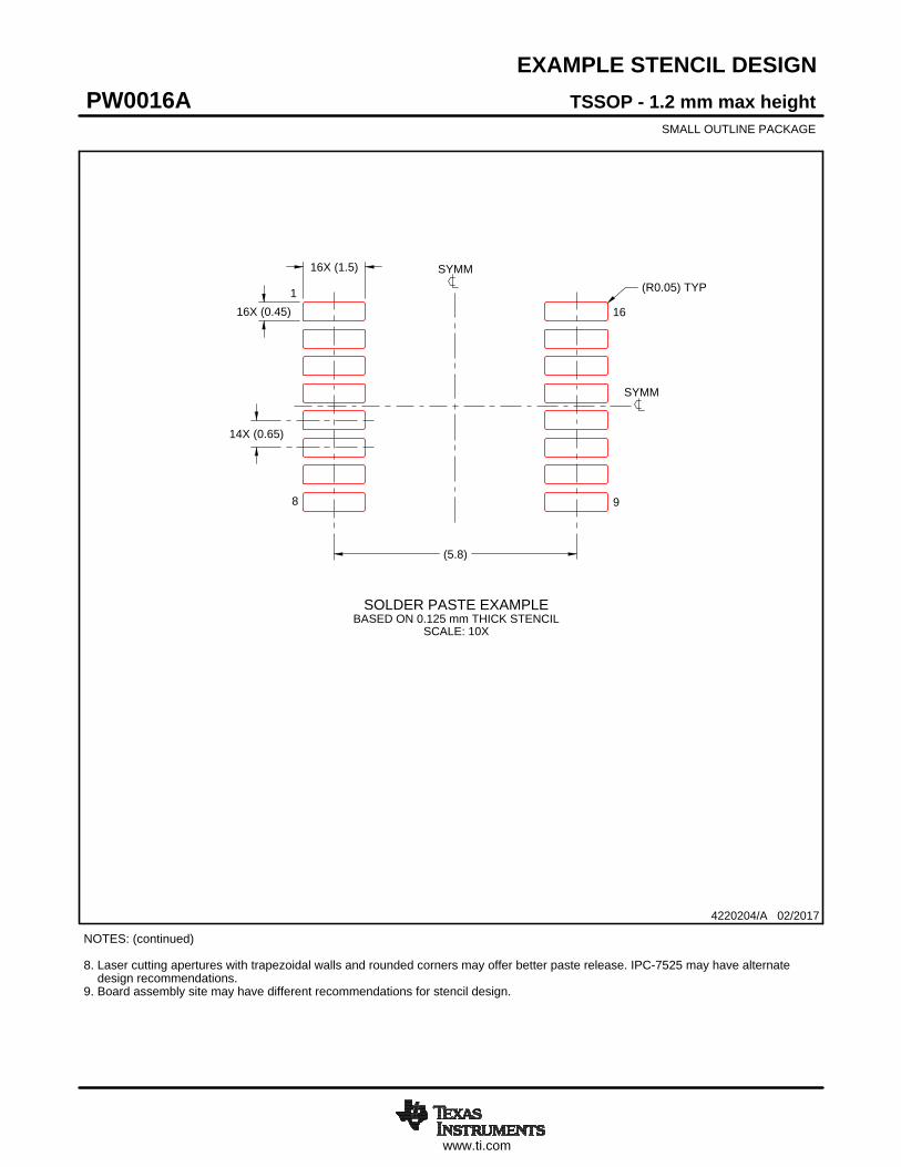
EXAMPLE STENCIL DESIGN
16X (1.5)
16X (0.45)
14X (0.65)
(5.8)
(R0.05) TYP
TSSOP - 1.2 mm max heightPW0016ASMALL OUTLINE PACKAGE
4220204/A 02/2017
NOTES: (continued) 8. Laser cutting apertures with trapezoidal walls and rounded corners may offer better paste release. IPC-7525 may have alternate design recommendations. 9. Board assembly site may have different recommendations for stencil design.
SOLDER PASTE EXAMPLEBASED ON 0.125 mm THICK STENCIL
SCALE: 10X
SYMM
SYMM
1
8 9
16
www.ti.com
GENERIC PACKAGE VIEW
This image is a representation of the package family, actual package may vary.Refer to the product data sheet for package details.
WQFN - 0.8 mm max heightBQB 16PLASTIC QUAD FLATPACK - NO LEAD2.5 x 3.5, 0.5 mm pitch
4226161/A
NOTES:
1. All linear dimensions are in millimeters. Any dimensions in parenthesis are for reference only. Dimensioning and tolerancingper ASME Y14.5M.
2. This drawing is subject to change without notice.3. The package thermal pad must be soldered to the printed circuit board for optimal thermal and mechanical performance.
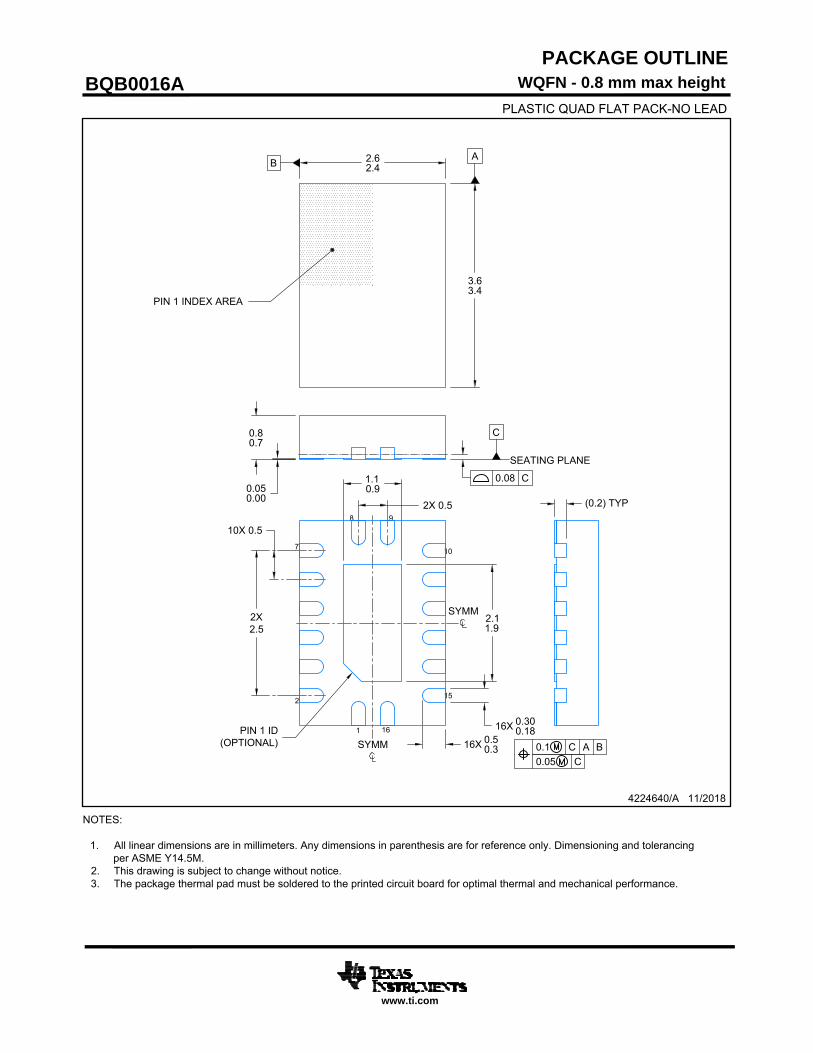
PACKAGE OUTLINE
4224640/A 11/2018
www.ti.com
WQFN - 0.8 mm max height
PLASTIC QUAD FLAT PACK-NO LEAD
BQB0016A
A
0.08 C
0.1 C A B0.05 C
B
SYMM
SYMM
PIN 1 INDEX AREA
2.62.4
3.63.4
0.80.7
0.050.00
SEATING PLANE
C
1.10.9
2.11.9
2X 0.5
16X 0.300.18
16X 0.50.3
2X2.5
10X 0.5
PIN 1 ID(OPTIONAL)
(0.2) TYP
1
2
7
8 9
10
15
16
AutoCAD SHX Text
AutoCAD SHX Text
NOTES: (continued)
4. This package is designed to be soldered to a thermal pad on the board. For more information, see Texas Instruments literaturenumber SLUA271 (www.ti.com/lit/slua271) .
5. Vias are optional depending on application, refer to device data sheet. If any vias are implemented, refer to their locations shown on this view. It is recommended that vias under paste be filled, plugged or tented.
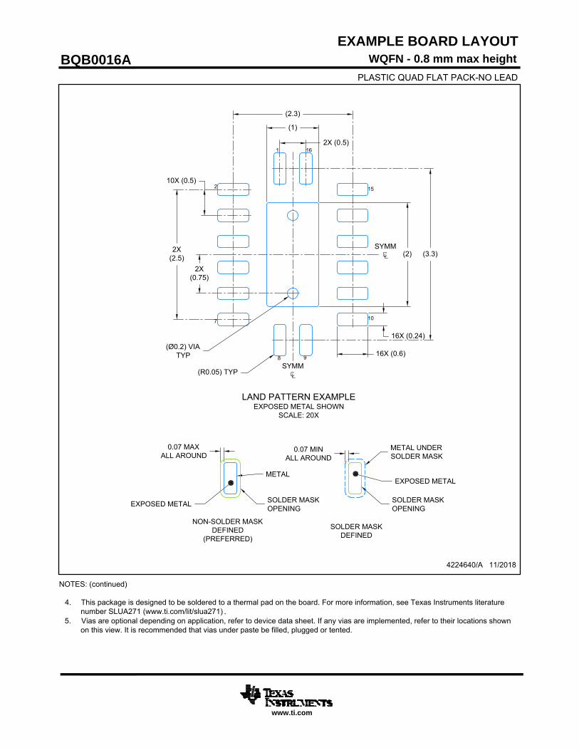
EXAMPLE BOARD LAYOUT
4224640/A 11/2018
www.ti.com
WQFN - 0.8 mm max height
BQB0016A
PLASTIC QUAD FLAT PACK-NO LEAD
SYMM
SYMM
LAND PATTERN EXAMPLEEXPOSED METAL SHOWN
SCALE: 20X
(1)
(2) (3.3)
16X (0.24)
16X (0.6)
2X(2.5)
10X (0.5)
2X (0.5)
(2.3)
2X(0.75)
(Ø0.2) VIATYP
(R0.05) TYP
1
2
7
8 9
10
15
16
0.07 MAXALL AROUND
0.07 MINALL AROUND
METAL
SOLDER MASKOPENING
METAL UNDERSOLDER MASK
SOLDER MASKOPENINGEXPOSED METAL
EXPOSED METAL
NON-SOLDER MASKDEFINED
(PREFERRED)SOLDER MASK
DEFINED
AutoCAD SHX Text
AutoCAD SHX Text

NOTES: (continued)
6. Laser cutting apertures with trapezoidal walls and rounded corners may offer better paste release. IPC-7525 may have alternatedesign recommendations.
EXAMPLE STENCIL DESIGN
4224640/A 11/2018
www.ti.com
WQFN - 0.8 mm max height
BQB0016A
PLASTIC QUAD FLAT PACK-NO LEAD
SOLDER PASTE EXAMPLEBASED ON 0.125 mm THICK STENCIL
EXPOSED PAD85% PRINTED COVERAGE BY AREA
SCALE: 20X
SYMM
SYMM
(0.95)
(1.79) (3.3)
16X (0.24)
16X (0.6)
2X(2.5)
10X (0.5)
2X (0.5)
(2.3)
(R0.05) TYP
1
2
7
8 9
10
15
16
EXPOSED METAL
AutoCAD SHX Text
AutoCAD SHX Text
NOTES:
1. All linear dimensions are in millimeters. Any dimensions in parenthesis are for reference only. Dimensioning and tolerancingper ASME Y14.5M.
2. This drawing is subject to change without notice.3. This dimension does not include mold flash, protrusions, or gate burrs. Mold flash, protrusions, or gate burrs shall not exceed
0.15 per side.4. This dimension does not include interlead flash. Interlead flash shall not exceed 0.50 per side.5. Reference JEDEC Registration MO-345, Variation AA
PACKAGE OUTLINE
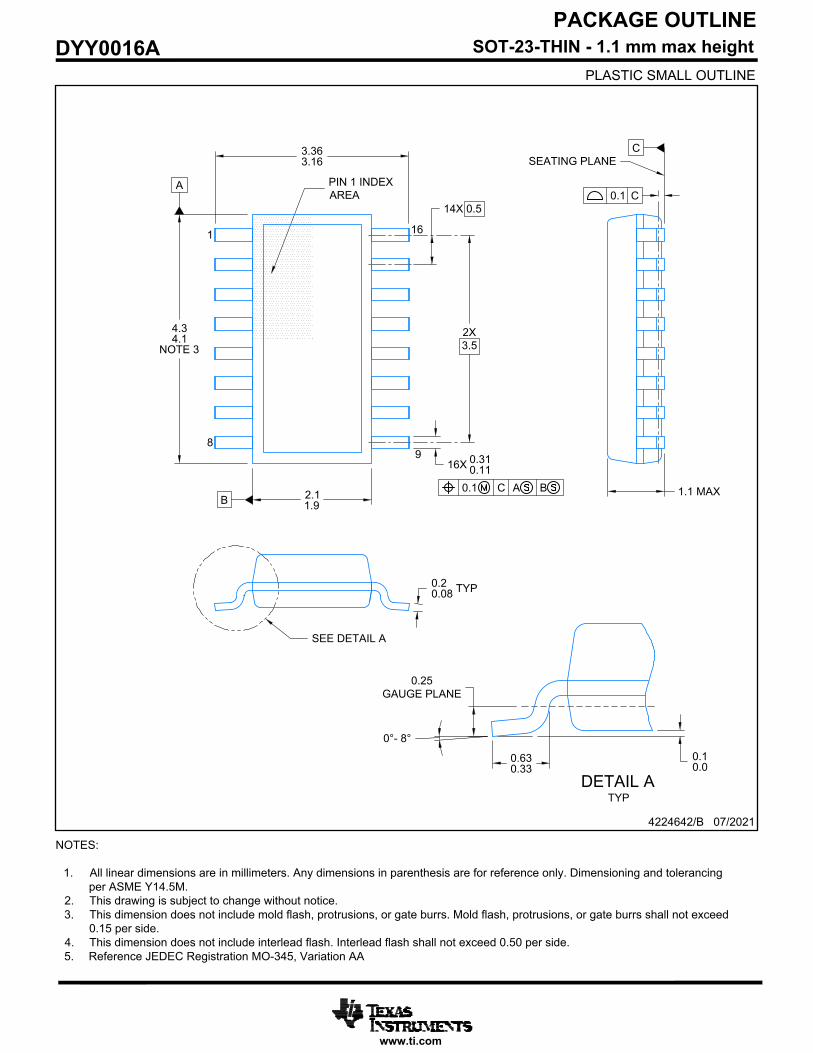
4224642/B 07/2021
www.ti.com
SOT-23-THIN - 1.1 mm max heightPLASTIC SMALL OUTLINE
DYY0016A
A0.1 C
B
PIN 1 INDEXAREA
4.34.1
NOTE 3
2.11.9
3.363.16
14X 0.5
2X3.5
16X 0.310.11
0.1 C A B 1.1 MAX
CSEATING PLANE
0.20.08 TYP
SEE DETAIL A
0.10.0
0.25GAUGE PLANE
0°- 8°
0.630.33
DETAIL ATYP
1
89
16
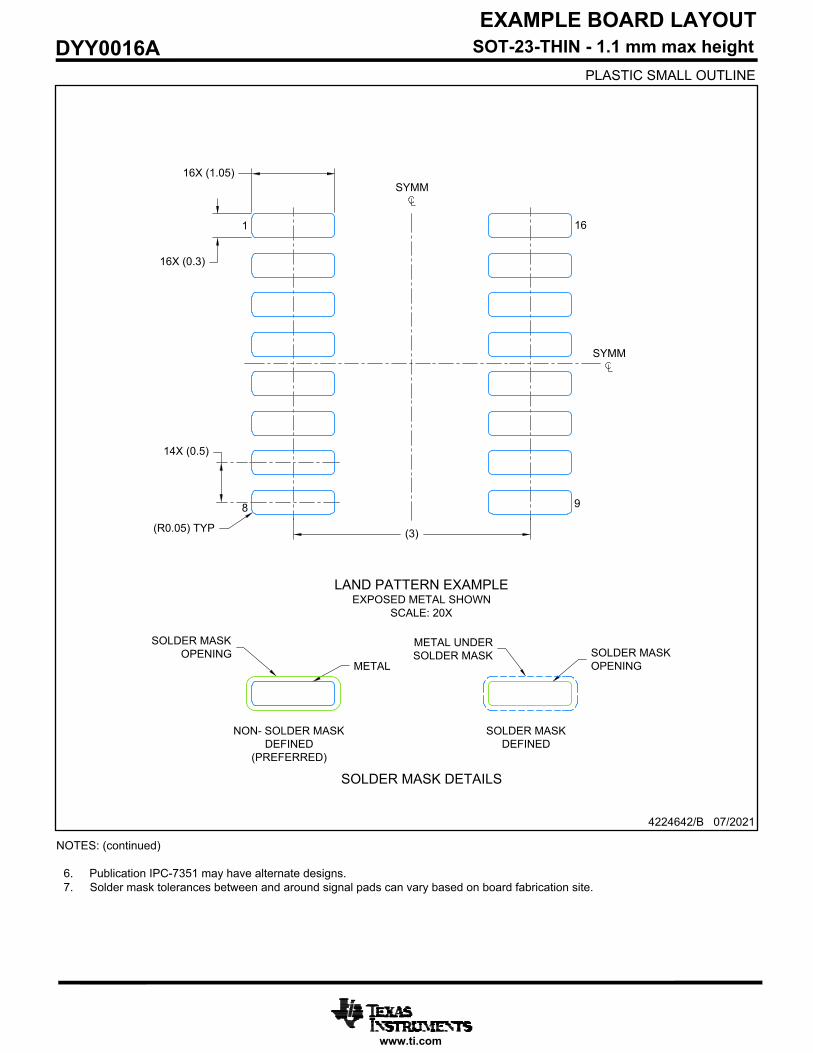
NOTES: (continued)
6. Publication IPC-7351 may have alternate designs. 7. Solder mask tolerances between and around signal pads can vary based on board fabrication site.
EXAMPLE BOARD LAYOUT
4224642/B 07/2021
www.ti.com
SOT-23-THIN - 1.1 mm max heightDYY0016APLASTIC SMALL OUTLINE
SYMM
SYMM
LAND PATTERN EXAMPLEEXPOSED METAL SHOWN
SCALE: 20X
16X (0.3)
16X (1.05)
(3)
14X (0.5)
(R0.05) TYP
1
8 9
16
METAL
SOLDER MASK OPENING SOLDER MASK
OPENING
METAL UNDERSOLDER MASK
NON- SOLDER MASKDEFINED
(PREFERRED)
SOLDER MASKDEFINED
SOLDER MASK DETAILS
AutoCAD SHX Text
AutoCAD SHX Text

NOTES: (continued) 8. Laser cutting apertures with trapezoidal walls and rounded corners may offer better paste release. IPC-7525 may have alternate
design recommendations. 9. Board assembly site may have different recommendations for stencil design.
EXAMPLE STENCIL DESIGN
4224642/B 07/2021
www.ti.com
SOT-23-THIN - 1.1 mm max heightDYY0016APLASTIC SMALL OUTLINE
SOLDER PASTE EXAMPLEBASED ON 0.125 mm THICK STENCIL
SCALE: 20X
SYMM
SYMM
16X (0.3)
16X (1.05)
(3)
14X (0.5)
(R0.05) TYP
1
8 9
16
AutoCAD SHX Text
AutoCAD SHX Text
IMPORTANT NOTICE AND DISCLAIMERTI PROVIDES TECHNICAL AND RELIABILITY DATA (INCLUDING DATA SHEETS), DESIGN RESOURCES (INCLUDING REFERENCE DESIGNS), APPLICATION OR OTHER DESIGN ADVICE, WEB TOOLS, SAFETY INFORMATION, AND OTHER RESOURCES “AS IS” AND WITH ALL FAULTS, AND DISCLAIMS ALL WARRANTIES, EXPRESS AND IMPLIED, INCLUDING WITHOUT LIMITATION ANY IMPLIED WARRANTIES OF MERCHANTABILITY, FITNESS FOR A PARTICULAR PURPOSE OR NON-INFRINGEMENT OF THIRD PARTY INTELLECTUAL PROPERTY RIGHTS.These resources are intended for skilled developers designing with TI products. You are solely responsible for (1) selecting the appropriate TI products for your application, (2) designing, validating and testing your application, and (3) ensuring your application meets applicable standards, and any other safety, security, regulatory or other requirements.These resources are subject to change without notice. TI grants you permission to use these resources only for development of an application that uses the TI products described in the resource. Other reproduction and display of these resources is prohibited. No license is granted to any other TI intellectual property right or to any third party intellectual property right. TI disclaims responsibility for, and you will fully indemnify TI and its representatives against, any claims, damages, costs, losses, and liabilities arising out of your use of these resources.TI’s products are provided subject to TI’s Terms of Sale or other applicable terms available either on ti.com or provided in conjunction with such TI products. TI’s provision of these resources does not expand or otherwise alter TI’s applicable warranties or warranty disclaimers for TI products.TI objects to and rejects any additional or different terms you may have proposed. IMPORTANT NOTICE
Mailing Address: Texas Instruments, Post Office Box 655303, Dallas, Texas 75265Copyright © 2022, Texas Instruments Incorporated
Related Documents