ADVANCE INFORMATION TMS320TCI6487 TMS320TCI6488 www.ti.com SPRS358L – APRIL 2007 – REVISED APRIL 2011 TMS320TCI6487/8 Communications Infrastructure Digital Signal Processor 1 Features 12 – Extended Temperature: • Key Features • 1.2-GHz Device: -40°C to 95°C – High-Performance Communications Infrastructure DSP (TCI6487/8) • 1.0-GHz Device: -40°C to 100°C – Instruction Cycle Time: 1.25 ns to 0.83 ns • 3 TMS320C64x+™ DSP Cores (1.2-GHz Device); 1.25 ns to 1 ns (1-GHz – Dedicated SPLOOP Instructions Device) – Compact Instructions (16-Bit) – Clock Rate: 800 MHz to 1.2 GHz (1.2-GHz – Exception Handling Device); 800-MHz to 1-GHz (1-GHz Device) • TMS320C64x+ Megamodule L1/L2 Memory – Commercial Temperature and Extended Architecture Temperature – 256 K-Bit (32 K-Byte) L1P Program Cache – 3 TMS320C64x+™ DSP Cores; Six RSAs for [Direct Mapped] CDMA Processing (2 per core) – 256 K-Bit (32 K-Byte) L1D Data Cache – One Receive Accelerator (RAC) [TCI6488 [2-Way Set-Associative] Only] – 24 M-Bit (3072 K-Byte) Total L2 Unified – Enhanced VCP2/TCP2 Mapped RAM/Cache [Flexible Allocation] – Frame Synchronization Interface • Configurable at boot-time to 1 MB/ – 16-/32-Bit DDR2-667 Memory Controller 1 MB/1 MB or 1.5 MB/1 MB/0.5 MB – EDMA3 Controller – 512 K-Bit (64 K-Byte) L3 ROM – Antenna Interface • One Receive Accelerator (RAC) [TCI6488 Only] – Two 1x Serial RapidIO ® Links, v1.2 – Performs Chip-Rate RX Functions Compliant – Up to 64 Macro-BTS Users – One 1.8-V Inter-Integrated Circuit (I2C) Bus – Up to 160 km cell size – Two 1.8-V McBSPs • Six RSAs for CDMA Processing (2 per core) – 1000 Mbps Ethernet MAC (EMAC) – Dedicated RAKE, PATH_SEARCH and – Six 64-Bit General-Purpose Timers RACH_SEARCH Instructions – 16 General-Purpose I/O (GPIO) Pins – Transmit Processing Capability – Internal Semaphore Module • Enhanced VCP2 – System PLL and PLL Controller/DDR PLL – Supports Over 694 7.95-Kbps AMR and PLL Controller, Dedicated to DDR2 • Enhanced Turbo Decoder Coprocessor (TCP2) Memory Controller – Supports up to Eight 2-Mbps 3 GPP • High-Performance Communications (6 Iterations) Infrastructure DSP (TCI6487/8) • Endianness: Little Endian, Big Endian – Instruction Cycle Time: • Frame Synchronization Interface • 1.2-GHz Device: 1.25-ns to 0.83-ns (1) – Time Alignment Between Internal • 1-GHz Device: 1.25-ns to 1-ns Subsystems, External Devices/System – Clock Rate: – OBSAI RP1 Compliant for Frame Burst Data • 1.2-GHz Device: 800-MHz to 1.2-GHz – Alternate Interfaces for non-RP1 and • 1-GHz Device: 800-MHz to 1-GHz non-UMTS Systems – Eight 32-Bit Instructions/Cycle • 16-/32-Bit DDR2-667 Memory Controller – Commercial Temperature: • EDMA3 Controller (64 Independent Channels) • 1.2-GHz Device: 0°C to 95°C • Antenna Interface • 1-GHz Device: 0°C to 100°C – 6 Configurable Links (Full Duplex) – Supports OBSAI RP3 Protocol, v1.0: (1) Note: Advance information is presented in this document for 768-Mbps, 1.536-, 3.072-Gbps Link Rates the TCI6487/8 1.2-GHz device. The TCI6487/8 1.0-GHz DSP – Supports CPRI Protocol V2.0: 614.4-Mbps, is a fully-qualified device. 1 Please be aware that an important notice concerning availability, standard warranty, and use in critical applications of Texas Instruments semiconductor products and disclaimers thereto appears at the end of this data sheet. 2All trademarks are the property of their respective owners. ADVANCE INFORMATION concerns new products in the sampling Copyright © 2007–2011, Texas Instruments Incorporated or preproduction phase of development. Characteristic data and other specifications are subject to change without notice.

Welcome message from author
This document is posted to help you gain knowledge. Please leave a comment to let me know what you think about it! Share it to your friends and learn new things together.
Transcript
AD
VA
NC
E I
NF
OR
MA
TIO
N
TMS320TCI6487TMS320TCI6488
www.ti.com SPRS358L–APRIL 2007–REVISED APRIL 2011
TMS320TCI6487/8 Communications Infrastructure Digital Signal Processor
1 Features12
– Extended Temperature:• Key Features• 1.2-GHz Device: -40°C to 95°C– High-Performance Communications
Infrastructure DSP (TCI6487/8) • 1.0-GHz Device: -40°C to 100°C– Instruction Cycle Time: 1.25 ns to 0.83 ns • 3 TMS320C64x+™ DSP Cores
(1.2-GHz Device); 1.25 ns to 1 ns (1-GHz – Dedicated SPLOOP InstructionsDevice) – Compact Instructions (16-Bit)
– Clock Rate: 800 MHz to 1.2 GHz (1.2-GHz – Exception HandlingDevice); 800-MHz to 1-GHz (1-GHz Device) • TMS320C64x+ Megamodule L1/L2 Memory
– Commercial Temperature and Extended ArchitectureTemperature – 256 K-Bit (32 K-Byte) L1P Program Cache
– 3 TMS320C64x+™ DSP Cores; Six RSAs for [Direct Mapped]CDMA Processing (2 per core) – 256 K-Bit (32 K-Byte) L1D Data Cache
– One Receive Accelerator (RAC) [TCI6488 [2-Way Set-Associative]Only] – 24 M-Bit (3072 K-Byte) Total L2 Unified
– Enhanced VCP2/TCP2 Mapped RAM/Cache [Flexible Allocation]– Frame Synchronization Interface • Configurable at boot-time to 1 MB/– 16-/32-Bit DDR2-667 Memory Controller 1 MB/1 MB or 1.5 MB/1 MB/0.5 MB– EDMA3 Controller – 512 K-Bit (64 K-Byte) L3 ROM– Antenna Interface • One Receive Accelerator (RAC) [TCI6488 Only]– Two 1x Serial RapidIO® Links, v1.2 – Performs Chip-Rate RX Functions
Compliant – Up to 64 Macro-BTS Users– One 1.8-V Inter-Integrated Circuit (I2C) Bus – Up to 160 km cell size– Two 1.8-V McBSPs • Six RSAs for CDMA Processing (2 per core)– 1000 Mbps Ethernet MAC (EMAC) – Dedicated RAKE, PATH_SEARCH and– Six 64-Bit General-Purpose Timers RACH_SEARCH Instructions– 16 General-Purpose I/O (GPIO) Pins – Transmit Processing Capability– Internal Semaphore Module • Enhanced VCP2– System PLL and PLL Controller/DDR PLL – Supports Over 694 7.95-Kbps AMR
and PLL Controller, Dedicated to DDR2 • Enhanced Turbo Decoder Coprocessor (TCP2)Memory Controller – Supports up to Eight 2-Mbps 3 GPP
• High-Performance Communications (6 Iterations)Infrastructure DSP (TCI6487/8) • Endianness: Little Endian, Big Endian– Instruction Cycle Time: • Frame Synchronization Interface
• 1.2-GHz Device: 1.25-ns to 0.83-ns (1)– Time Alignment Between Internal
• 1-GHz Device: 1.25-ns to 1-ns Subsystems, External Devices/System– Clock Rate: – OBSAI RP1 Compliant for Frame Burst Data
• 1.2-GHz Device: 800-MHz to 1.2-GHz – Alternate Interfaces for non-RP1 and• 1-GHz Device: 800-MHz to 1-GHz non-UMTS Systems
– Eight 32-Bit Instructions/Cycle • 16-/32-Bit DDR2-667 Memory Controller– Commercial Temperature: • EDMA3 Controller (64 Independent Channels)
• 1.2-GHz Device: 0°C to 95°C • Antenna Interface• 1-GHz Device: 0°C to 100°C – 6 Configurable Links (Full Duplex)
– Supports OBSAI RP3 Protocol, v1.0:(1) Note: Advance information is presented in this document for 768-Mbps, 1.536-, 3.072-Gbps Link Rates
the TCI6487/8 1.2-GHz device. The TCI6487/8 1.0-GHz DSP – Supports CPRI Protocol V2.0: 614.4-Mbps,is a fully-qualified device.1
Please be aware that an important notice concerning availability, standard warranty, and use in critical applications of TexasInstruments semiconductor products and disclaimers thereto appears at the end of this data sheet.
2All trademarks are the property of their respective owners.
ADVANCE INFORMATION concerns new products in the sampling Copyright © 2007–2011, Texas Instruments Incorporatedor preproduction phase of development. Characteristic data and otherspecifications are subject to change without notice.
AD
VA
NC
E IN
FO
RM
AT
ION
AB
CD
EF
GH
JK
LM
NP
RT
UV
WY
AAAB
ACAD
AE
AFAG
2
1 3
4
5
6
7
8
9
10
11
12
13
14
15
16
17
18
19
20
21
22
23
24
25
26
27
TMS320TCI6487TMS320TCI6488SPRS358L–APRIL 2007–REVISED APRIL 2011 www.ti.com
1.2288-, 2.4576-Gbps Link Rates – Configurable in a Watchdog Timer mode– Clock Input Independent or Shared with CPU • 16 General-Purpose I/O (GPIO) Pins
(Selectable at Boot-Time) • Internal Semaphore Module• Two 1x Serial RapidIO® Links, v1.2 Compliant – Software Method to Control Access to
– 1.25-, 2.5-, 3.125-Gbps Link Rates Shared Resources– Message Passing and DirectIO Support – 32 General Purpose Semaphore Resources– Error Management Extensions and • System PLL and PLL Controller
Congestion Control • DDR PLL and PLL Controller, Dedicated to• One 1.8-V Inter-Integrated Circuit (I2C) Bus DDR2 Memory Controller• Two 1.8-V McBSPs • IEEE-1149.1 and IEEE-1149.6 (JTAG™)
Boundary-Scan-Compatible• 1000 Mbps Ethernet MAC (EMAC)• 561-Pin Ball Grid Array (BGA) Packages (CUN,– IEEE 802.3 Compliant
GUN, or ZUN Suffix), 0.8-mm Ball Pitch– Supports SGMII, v1.8 Compliant• 0.065-μm/7-Level Cu Metal Process (CMOS)– 8 Independent Transmit (TX) and 8• SmartReflex™ Class 0 - 0.9-V to 1.2-V AdaptiveIndependent Receive (RX) Channels
Core Voltage• Six 64-Bit General-Purpose Timers• 1.8-V, 1.1-V I/Os– Configurable up to Twelve 32-Bit Timers
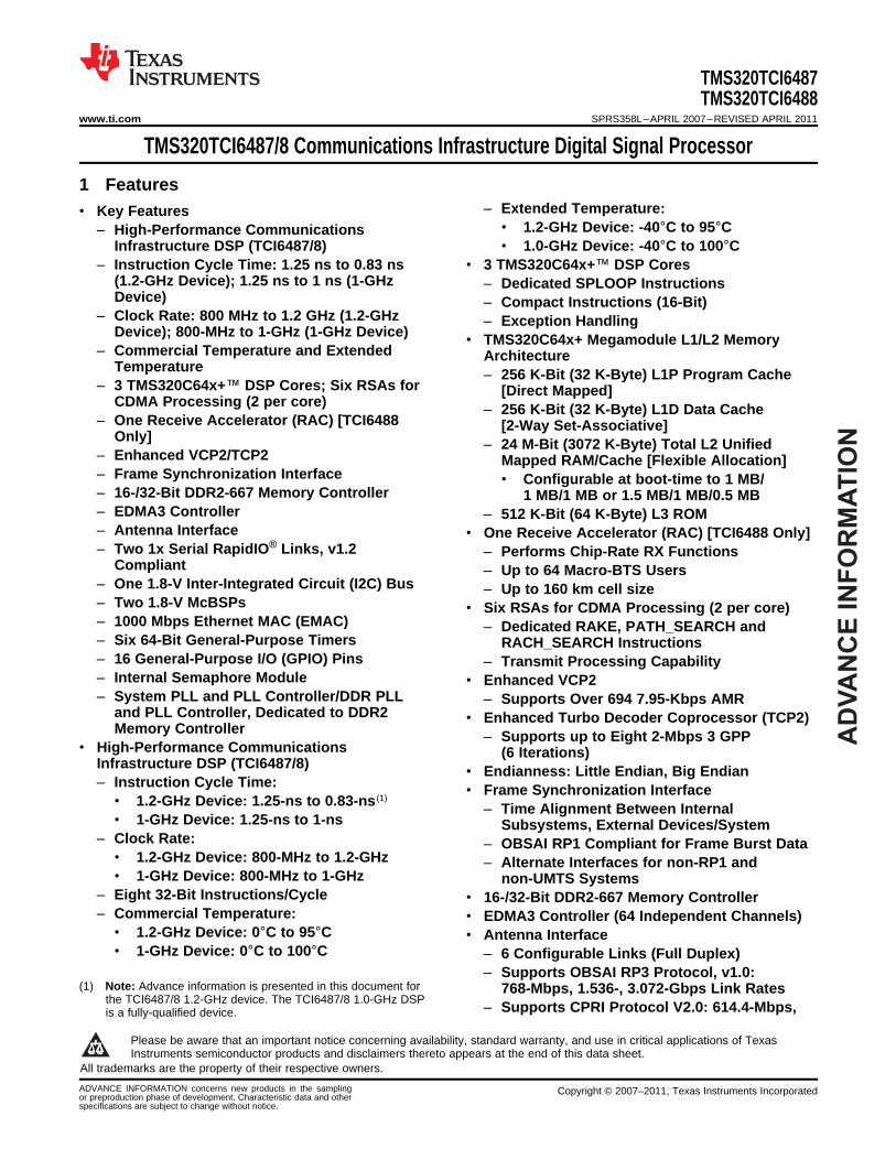
1.1 CUN/GUN/ZUN BGA Package (Bottom View)
The devices are designed for a package temperature range of 0°C to 100°C (commercial temperaturerange; 1-GHz device), -40°C to 100°C (extended temperature range; 1-GHz device), 0°C to 95°C(commercial temperature range; 1.2-GHz device), and -40°C to 95°C (extended temperature range;1.2-GHz device). A heatsink is required so that this range is not exceeded.
Figure 1-1. CUN/GUN/ZUN 561-Pin BGA Package (Bottom View)
2 Features Copyright © 2007–2011, Texas Instruments Incorporated
Submit Documentation FeedbackProduct Folder Link(s): TMS320TCI6487
AD
VA
NC
E I
NF
OR
MA
TIO
N
TMS320TCI6487TMS320TCI6488
www.ti.com SPRS358L–APRIL 2007–REVISED APRIL 2011
1.2 Description
The TMS320C64x+ DSPs (including the TMS320TCI6487/8 device) are the highest-performancecommunications infrastructure DSP generation in the TMS320C6000™ DSP platform.
The TCI6487/8 device is based on the third-generation high-performance, advanced VelociTI™very-long-instruction-word (VLIW) architecture developed by Texas Instruments (TI). It is designedspecifically for wireless infrastructure baseband applications, providing an ideal platform for UMTS,TD-SCDMA, Wi-MAX and GSM/EDGE Macro, Micro, Pico, and Enterprise BTS; moreover, the deviceenables System-on-Chip (SoC) solutions in video and telecom infrastructure and medical imagingapplications.
The C64x+™ devices are upward code-compatible from previous devices that are part of the C6000™DSP platform.
1.2.1 Core Processor
Based on 65-nm process technology and 3.6 GHz of total raw DSP processing power with performance ofup to 28,800 million instructions per second (MIPS) [or 28,800 16-bit MMACs per cycle], the TCI6487/8device offers cost-effective solutions to high-performance DSP programming challenges with threeindependent DSP subsystems. The DSP possesses the operational flexibility of high-speed controllers andnumerical capability of array processors.
The C64x+ DSP core employs eight functional units, two register files, and two data paths. Like the earlierC6000 devices, two of these functional units are multipliers or .M units. Each C64x+ .M unit doubles themultiply throughput versus the C64x core by performing four 16-bit x 16-bit multiply-accumulates (MACs)every clock cycle. Thus, eight 16-bit x 16-bit MACs can be executed every cycle on the C64x+ core. Ata1.2-GHz rate, this means 9600 16-bit MMACs can occur every microsecond. Moreover, each multiplieron the C64x+ core can compute one 32-bit x 32-bit MAC or four 8-bit x 8-bit MACs every clock cycle.
The TCI6487/8 DSP integrates a large amount of on-chip memory organized as a three-level memorysystem. The level-1 data memories on the device are 32 KB each. This memory can be configured asmapped RAM, cache, or some combination of the two. When configured as cache, L1 program (L1P) is adirect-mapped cache where as L1 data (L1D) is a two-way set associative cache. The level-2 (L2)memory is shared between program and data space for a total of 3 MB of SRAM/cache with twoconfigurations. L2 memory can be configured as 1 MB/1 MB/1 MB or 1.5 MB/1 MB/0.5 MB among thethree DSP cores. The level-3 (L3) ROM is 64 KB in the device. The C64x+ megamodule also has a 32-bitperipheral configuration (CFG) port, an internal DMA (IDMA) controller, a system component withreset/boot control, and a free-running 64 -bit timer for time stamp.
The C64x+ DSP core has a complete set of development tools which includes: a new C compiler, anassembly optimizer to simplify programming and scheduling, and a Windows® debugger interface forvisibility into source code execution.
The DMA switch fabric provides enhanced on-chip connectivity between the DSP cores and theperipherals and accelerators.
1.2.2 Peripherals
The peripheral set includes: an inter-integrated circuit bus module (I2C); two multichannel buffered serialports (McBSPs) each at 100 Mbps; six 64-bit general-purpose timers (also configurable as twelve 32-bittimers); 16 general-purpose input/output ports (GPIO) with programmable interrupt/event generationmodes; a 1000-Mbps Ethernet media access controller (EMAC), which provides an efficient interfacebetween the TCI6487/8 DSP core processor and the network; a management data input/output (MDIO)module (also part of EMAC), which controls PHY configuration and status monitoring; a framesynchronization (FSYNC) module, which synchronizes DMA transactions; a semaphore hardware block(Semaphore), which allows access to shared resources with unique interrupts to each of the cores toidentify when that core has acquired the resource; and a 16-/32-bit DDR2 SDRAM interface.
The I2C port allows the DSP to easily control peripheral devices and communicate with a host processor.
Copyright © 2007–2011, Texas Instruments Incorporated Features 3Submit Documentation Feedback
Product Folder Link(s): TMS320TCI6487
AD
VA
NC
E IN
FO
RM
AT
ION
TMS320TCI6487TMS320TCI6488SPRS358L–APRIL 2007–REVISED APRIL 2011 www.ti.com
The device includes two Serial RapidIO® (SRIO) with link rates of 1.25 Gbps, 2.5 Gbps or 3.125 Gbps.This high-bandwidth peripheral is used for point-to-point inter-device communication and may connect theTCI6487/8 device to other DSPs, ASICs, or switches on the same board or across the backplane. Thisdramatically improves system performance and reduces system cost for applications that include multipleDSPs on a board such as video and telecom infrastructures and medical/imaging. The SRIO also providesalarm, interrupt, and messaging events.
The device includes the SerDes-based antenna interface (AIF) capable of up to 3.072 Gbps operation perlink. The AIF comprises six high-speed serial links, compliant to OBSAI RP3 and CPRI standards. Theantenna interface is used to connect the backplane for antenna data transmission and reception. Each linkof the AIF includes a differential receive and transmit signal pair.
1.2.3 Accelerators
The device has two high-performance embedded coprocessors [enhanced Viterbi Decoder Coprocessor(VCP2) and enhanced turbo decoder coprocessor (TCP2)] that significantly speed up channel-decodingoperations on-chip. The VCP2 operating at CPU clock divided-by-3 can decode over 694 7.95-Kbpsadaptive multi-rate (AMR) [K=9, R=1/3] voice channels. The VCP2 supports constraint lengths K = 5, 6, 7,8, and 9, rates R = 3/4, 1/2, 1/3, and 1/5, and flexible polynomials, while generating hard decisions or softdecisions. The TCP2 operating at CPU clock divided-by-3 can decode up to fifty 384-Kbps or eight2-Mbps turbo encoded channels (assuming 6 iterations). The TCP2 implements the max*log-mapalgorithm and is designed to support all polynomials and rates required by third-generation partnershipprojects (3 GPP and 3 GPP2), with fully programmable frame length and turbo interleaver. Decodingparameters such as the number of iterations and stopping criteria are also programmable.Communications between the VCP2/TCP2 and the CPU are carried out through the EDMA3 controller.
The C64x+ CPU has six rake/search accelerators (RSAs) for code division multiple access (CDMA) toassist with chip rate processing in base transceiver systems (BTS).
The TCI6488 device also has a receive acceleration coprocessor (RAC) subsystem which includes thecomponents: 2 GCCP correlation accelerators; a back-end interface (BEI) for management of the RACconfiguration and data output; and a front-end interface (FEI) for reception of the antenna data forprocessing and access to all memory-mapped registers (MMRs) and memories in the RAC components.
4 Features Copyright © 2007–2011, Texas Instruments Incorporated
Submit Documentation FeedbackProduct Folder Link(s): TMS320TCI6487
AD
VA
NC
E I
NF
OR
MA
TIO
N
DSP Subsystem 2
C64x+ Megamodule
Po
we
r C
on
tro
lS
ys
tem
L1P Memory Controller (Memory Protect/Bandwidth Mgmt)
Instruction Fetch
EDMA 3.0
A Register File
A31 - A16
A15 - A0
B Register File
B31 - B16
B15 - B0
.L1 .S1.M1xxxx
.D1
C64x+ DSP Core
Inte
rru
pt
Ex
ce
pti
on
Co
ntr
oll
er
L2
Me
mo
ry C
on
tro
lle
r(M
em
ory
Pro
tec
t/B
an
dw
idth
Mg
mt)
Inte
rna
l D
MA
(DM
A)
32K BytesL1P SRAM/Cache
Direct-Mapped
L2/Cache0.5 - 1.5 M
32K Bytes TotalL1D SRAM/Cache 2-Way
Set Associative
RSA RSA
PLL1 andPLL1 Controller
SemaphoreRAC(A)
Power-Down and DeviceConfiguration Logic
L3 ROM
Boot Configuration
Sw
itc
he
dC
en
tra
lR
es
ou
rce
(SC
R)
DDR2 MemoryController
PLL2
Serial RapidIO(2x)
TCP2
VCP2
McBSP0
EMAC
10/100/1000
SGMII
MDIO
Timer [0-5]
I2C
GPIO16
FSYNC
AntennaInterface
32
DD
R2
SD
RA
M
L1 Data Memory Controller (Memory Protect/Bandwidth Mgmt)
DSP Subsystem 1
DSP Subsystem 0
2
McBSP1
16
.D2.M2xxxx
.S2 .L2
16-/32-bitInstruction Dispatch
Instruction Decode
Control Registers
SPLOOP Buffer
In-Circuit Emulation
TMS320TCI6487TMS320TCI6488
www.ti.com SPRS358L–APRIL 2007–REVISED APRIL 2011
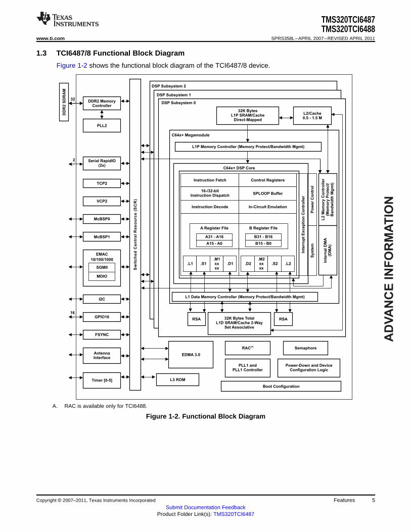
1.3 TCI6487/8 Functional Block Diagram
Figure 1-2 shows the functional block diagram of the TCI6487/8 device.
A. RAC is available only for TCI6488.
Figure 1-2. Functional Block Diagram
Copyright © 2007–2011, Texas Instruments Incorporated Features 5Submit Documentation Feedback
Product Folder Link(s): TMS320TCI6487
AD
VA
NC
E IN
FO
RM
AT
ION
TMS320TCI6487TMS320TCI6488SPRS358L–APRIL 2007–REVISED APRIL 2011 www.ti.com
1 Features ................................................... 1 5.7 Megamodule Revision .............................. 66
1.1 CUN/GUN/ZUN BGA Package (Bottom View) ....... 2 5.8 C64X+ Megamodule Register Description(s) ....... 671.2 Description ........................................... 3 6 Rake Search Accelerator (RSA) .................... 751.3 TCI6487/8 Functional Block Diagram ................ 5 7 Device Operating Conditions ....................... 76
7.1 Absolute Maximum Ratings Over Operating CaseRevision History .............................................. 7Temperature Range (Unless Otherwise Noted) .... 762 Device Overview ........................................ 8
7.2 Recommended Operating Conditions .............. 772.1 Device Characteristics ............................... 87.3 Electrical Characteristics Over Recommended2.2 CPU (DSP Core) Description ........................ 9 Ranges of Supply Voltage and Operating Case
2.3 Memory Map Summary ............................. 12 Temperature (Unless Otherwise Noted) ............ 782.4 Boot Sequence ..................................... 15 8 Peripheral Information and Electrical
Specifications .......................................... 792.5 Pin Assignments .................................... 18
8.1 Parameter Information .............................. 792.6 Signal Groups Description .......................... 228.2 Recommended Clock and Control Signal Transition
2.7 Terminal Functions ................................. 27Behavior ............................................ 80
2.8 Development and Device Support .................. 428.3 Power Supplies ..................................... 80
2.9 Documentation Support ............................ 438.4 Peripheral IDs (PIDs) ............................... 83
2.10 Community Resources ............................. 45 8.5 Enhanced Direct Memory Access (EDMA3)3 Device Configuration ................................. 46 Controller ........................................... 84
8.6 Interrupts .......................................... 1083.1 Device Configuration at Device Reset .............. 46
8.7 Reset Controller ................................... 1173.2 Peripheral Selection After Device Reset ........... 468.8 PLL1 and PLL1 Controller ......................... 1223.3 Device State Control Registers ..................... 478.9 PLL2 and PLL2 Controller ......................... 135
3.4 Device Status Register Descriptions ............... 488.10 DDR2 Memory Controller ......................... 137
3.5 Inter-DSP Interrupt Registers (IPCGR0-IPCGR28.11 I2C Peripheral ..................................... 140
and IPCAR0-IPCAR2) .............................. 508.12 Multichannel Buffered Serial Port (McBSP) ....... 145
3.6 JTAG ID (JTAGID) Register Description ........... 518.13 Ethernet MAC (EMAC) ............................ 154
3.7 Debugging Considerations ......................... 51 8.14 Management Data Input/Output (MDIO) .......... 1624 System Interconnect .................................. 52 8.15 Timers ............................................. 164
4.1 Internal Buses, Switch Fabrics, and 8.16 Enhanced Viterbi-Decoder Coprocessor (VCP2)Bridges/Gaskets .................................... 52 ..................................................... 173
8.17 Enhanced Turbo Decoder Coprocessor (TCP2)4.2 Data Switch Fabric Connections ................... 53..................................................... 175
4.3 Configuration Switch Fabric ........................ 568.18 Serial RapidIO (SRIO) Port ....................... 177
4.4 Priority Allocation ................................... 58 8.19 General Purpose Input/Output (GPIO) ............ 1895 C64x+ Megamodule ................................... 59 8.20 Emulation Features and Capability ............... 190
5.1 Megamodule Diagram .............................. 59 8.21 Semaphore ........................................ 194
5.2 Memory Architecture ............................... 60 8.22 Antenna Interface Subsystem ..................... 197
8.23 Frame Synchronization ............................ 2105.3 Memory Protection ................................. 63
8.24 RAC (TCI6488 Only) .............................. 2145.4 Bandwidth Management ............................ 659 Mechanical Data ...................................... 2155.5 Power-Down Control ............................... 66
9.1 Thermal Data ...................................... 2155.6 Megamodule Resets ................................ 669.2 Packaging Information ............................ 215
6 Contents Copyright © 2007–2011, Texas Instruments Incorporated
Submit Documentation FeedbackProduct Folder Link(s): TMS320TCI6487

AD
VA
NC
E I
NF
OR
MA
TIO
N
TMS320TCI6487TMS320TCI6488
www.ti.com SPRS358L–APRIL 2007–REVISED APRIL 2011
Revision HistoryNOTE: Page numbers for previous revisions may differ from page numbers in the current version.
This data manual revision history highlights the technical changes made to the data manual in thisrevision.
Scope: Applicable updates to the C64x device family, specifically relating to the TMS320TCI6487/8device, have been incorporated.
TCI6487/8 Revision HistorySEE ADDITIONS/MODIFICATIONS/DELETIONS
Section 8.13.2 EMAC Peripheral Register Descriptions:Corrected starting address for Table 8-57, EMAC Descriptor MemoryModified Table 8-59, EMAC Interrupt Control (EMIC) Registers
Copyright © 2007–2011, Texas Instruments Incorporated Contents 7Submit Documentation Feedback
Product Folder Link(s): TMS320TCI6487

AD
VA
NC
E IN
FO
RM
AT
ION
TMS320TCI6487TMS320TCI6488SPRS358L–APRIL 2007–REVISED APRIL 2011 www.ti.com
2 Device Overview
2.1 Device Characteristics
Table 2-1 provides an overview of the TCI6487/8 DSP. The tables show significant features of theTCI6487/8 device, including the capacity of on-chip RAM, the peripherals, the CPU frequency, and thepackage type with pin count.
Table 2-1. Characteristics of the TCI6487/8 Processor
HARDWARE FEATURES TCI6487/8
Peripherals DDR2 Memory Controller (32-bit bus width) [1.8 V I/O] 1Not all peripherals pins (clock memory = DDRREFCLK(N|P)are available at the same EDMA3 (64 independent channels [CPU/3 clock rate] 1time.
High-speed 1x Serial RapidIO Port (2 lanes) 1(For more detail, seeSection 3, Device I2C 1Configuration)
McBSPs 2(internal or external clock source up to 100 Mbps)
1000 Ethernet MAC (EMAC) 1
Management Data Input/Output (MDIO) 1
Antenna Interface (AIF) 1
Frame Synchronization (FSYNC) 1
64-bit Timers (Configurable) 6 64-bit or 12 32-bit(internal clock source CPU/6 clock frequency)
SYSCLKOUT 1
General Purpose Input/Output Port (GPIO) 16
Decoder Coprocessors VCP2 (clock source = CPU/3 clock frequency) 1
TCP2 (clock source = CPU/3 clock frequency) 1
Accelerators Receive Accelerator (RAC) (TCI6488 Only) 1
Rake/Search Accelerator 6
On-Chip Memory Size (Bytes) 3200 KB
Organization 32KB L1P Program Cache (SRAM/Cache)32KB L1D Data Cache (SRAM/Cache)
32KB Data Memory Controller3072KB Total L2 Unified Memory SRAM/Cache
64KB L3 ROM
CPU Megamodule Revision ID Register 0x0Revision ID (MM_REVID. [15:0]) 0x0181 2000)
JTAG Device_ID JTAG Register (address location: 0x0288 0814) For details, see Section 3.6
Frequency MHz 800 - 1200 (800 MHz to 1.2 GHz)
Cycle Time ns 1.25 ns - 0.83 ns (800 MHz to 1.2 GHz CPU)
Voltage Core (V) 0.9-V to 1.2-V SmartReflex (1) 1.1 V
I/O (V) 1.8 V, 1.1 V
PLL1 and PLL1 Controller CLKIN1 Frequency Multiplier Bypass (x1), (x4 to x32)Options
PLL2 DDR Clock X10
BGA Package 23 X 23 mm 561-Pin Flip-Chip with BGA CUN/GUN/ZUN
Process Technology μm 0.065 μm
(1) A heatsink and implementation of the SmartReflex solution is required for proper device operation. For more details on SmartReflex, seeSection 8.3.4.
8 Device Overview Copyright © 2007–2011, Texas Instruments Incorporated
Submit Documentation FeedbackProduct Folder Link(s): TMS320TCI6487

AD
VA
NC
E I
NF
OR
MA
TIO
N
TMS320TCI6487TMS320TCI6488
www.ti.com SPRS358L–APRIL 2007–REVISED APRIL 2011
Table 2-1. Characteristics of the TCI6487/8 Processor (continued)
HARDWARE FEATURES TCI6487/8
Product Status (1) Product Preview (PP), Advance Information (AI), or AIProduction Data (PD)
Device Part Numbers (For more details on C64x+ DSP part numbering, see TMS320TCI6487CUN/GUN/ZUNFigure 2-11) TMS320TCI6488CUN/GUN/ZUN
(1) ADVANCE INFORMATION concerns new products in the sampling or preproduction phase of development. Characteristic data andother specifications are subject to change without notice. Note: Advance information is presented in this document for the TCI6487/81.2-GHz device. The TCI6487/8 1.0-GHz DSP is a fully-qualified device.
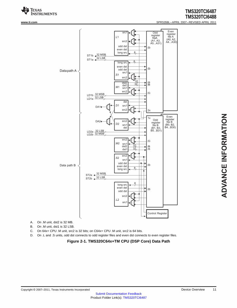
2.2 CPU (DSP Core) Description
The C64x+ central processing unit (CPU) consists of eight functional units, two register files, and two datapaths as shown in Figure 2-1. The two general-purpose register files (A and B) each contain 32 (thirty-two)32-bit registers for a total of 64 registers. The general-purpose registers can be used for data or can bedata address pointers. The data types supported include packed 8-bit data, 32-bit data, 40-bit data, and64-bit data. Values larger than 32 bits, such as 40-bit-long or 64-bit-long values are stored in registerpairs, with the 32 LSBs of data placed in an even register and the remaining 8 or 32 MSBs in the nextupper register (which is always an odd-numbered register).
The eight functional units (.M1, .L1, .D1, .S1, .M2, .L2, .D2, and .S2) are each capable of executing oneinstruction every clock cycle. The .M functional units perform all multiply operations. The .S and .L unitsperform a general set of arithmetic, logical, and branch functions. The .D units primarily load data frommemory to the register file and store results from the register file into memory.
The C64x+ CPU extends the performance of the C64x core through enhancements and new features.
Each C64x+ .M unit can perform one of the following each clock cycle: one 32 x 32 bit multiply, two 16 x16 bit multiplies, two 16 x 32 bit multiplies, four 8 x 8 bit multiplies, four 8 x 8 multiplies with addoperations and four 16 x 16 multiplies with add/subtract capabilities (including a complex multiply). Thereis also support for Galois filed multiplication for 8-bit and 32-bit data. Many communications algorithmssuch FFTs and modems require complex multiplication. The complex multiply (CMPY) instruction takesfour 16-bit inputs and produces a 32-bit real and a 32-bit imaginary output. There are also complexmultiplies with rounding capability that produces one 32-bit packed output that contain 16-bit real and16-bit imaginary values. The 32 x 32 bit multiply instructions provide the extended precision necessary foraudio and other high-precision algorithms on a variety of signed and unsigned 32-bit data types.
The .L or arithmetic logic unit now incorporates the ability to do parallel add/subtract operations on a pairof common inputs. Versions of this instruction exist to work on 32-bit data or on pairs of 16-bit dataperforming dual 16-bit add and subtracts in parallel. There are also saturated forms of these instructions.
The C64x+ core enhances the .S unit in several ways. In the C64x core, dual 16-bit MIN2 and MAX2comparisons were only available on the .L units. On the C64X+ core, they are also available on the .S unitwhich increases the performance of algorithms that do searching and sorting. Finally, to increase datapacking and unpacking throughput, the .S unit allows sustained high performance for the quad 8-bit/16-bitand dual 16-bit instructions. Unpack instructions prepare 8-bit data for parallel 16-bit operations. Packinstructions return parallel results to output precision including saturation support.
Other new features include:• SPLOOP - a small instruction buffer in the CPU that aids in creation of software pipelining loops where
multiple iterations of a loop are executed in parallel. The SPLOOP buffer reduces the code sizeassociated with software pipelining. Furthermore, loops in the SPLOOP buffer are fully interruptible.
• Compact Instructions - The native instruction size of the C6000 devices is 32 bits. Many commoninstructions such as MPY, AND, OR, ADD, and SUB can be expressed as 16 bits if the C64x+compiler can restrict the code to use certain registers in the register file. This compression isperformed by the code generation tools.
Copyright © 2007–2011, Texas Instruments Incorporated Device Overview 9Submit Documentation Feedback
Product Folder Link(s): TMS320TCI6487

AD
VA
NC
E IN
FO
RM
AT
ION
TMS320TCI6487TMS320TCI6488SPRS358L–APRIL 2007–REVISED APRIL 2011 www.ti.com
• Instruction Set Enhancements - As noted above, there are new instructions such as 32-bitmultiplications, complex multiplications, packing, sorting, bit manipulation, and 32-bit Galois fieldmultiplication.
• Exception Handling - Intended to aid the programmer in isolating bugs. The C64x+ CPU is able todetect and respond to exceptions, both from internally detected sources (such as illegal op-codes) andfrom system events (such as watchdog time expiration).
• Privilege - Defines user and supervisor modes of operation, allowing the operating system to give abasic level of protection to sensitive resources. Local memory is divided into multiple pages, each withread, write, and execute permissions.
• Time-Stamp Counter - Primarily targeted for real-time operating system (RTOS) robustness, afree-running time-stamp counter is implemented in the CPU that is not sensitive to system stalls.
For more details on the C64x+ CPU and its enhancements over the C64x architecture, see the followingdocuments:• TMS320C64x/C64x+ DSP CPU and Instruction Set Reference Guide (literature number SPRU732)• TMS320C64x+ DSP Cache User's Guide (literature number SPRU862)• TMS320C64x+ Megamodule Reference Guide (literature number SPRU871)• TMS320C64X to TMS320C64x+ CPU Migration Guide (literature number SPRAA84)
10 Device Overview Copyright © 2007–2011, Texas Instruments Incorporated
Submit Documentation FeedbackProduct Folder Link(s): TMS320TCI6487
AD
VA
NC
E I
NF
OR
MA
TIO
N
src2
src2
.D1
.M1
.S1
.L1
long src
odd dst
src2
src1
src1
src1
src1
even dst
even dstodd dst
dst1
dst
src2
src2
src2
long src
DA1
ST1b
LD1b
LD1a
ST1a
Datapath A
OddregisterfileA
(A1, A3,A5...A31)
Oddregisterfile B
(B1, B3,B5...B31)
.D2 src1dst
src2DA2
LD2aLD2b
src2
.M2 src1
dst1
.S2src1
even dstlong src
odd dst
ST2a
ST2b
long src
.L2
even dst
odd dst
src1
Data path B
Control Register
32 MSB
32 LSB
dst2 (A)
32 MSB
32 LSB
2x
1x
32 LSB32 MSB
32 LSB
32 MSB
dst2
(B)
(B)(A)
8
8
8
8
3232
3232
(C)
(C)
Evenregisterfile A
(A0, A2,A4...A30)
Evenregisterfile B
(B0, B2,B4...B30)
(D)
(D)
(D)
(D)
TMS320TCI6487TMS320TCI6488
www.ti.com SPRS358L–APRIL 2007–REVISED APRIL 2011
A. On .M unit, dst2 is 32 MB.B. On .M unit, dst1 is 32 LSB.C. On 64x+ CPU .M unit, src2 is 32 bits; on C64x+ CPU .M unit, src2 is 64 bits.D. On .L and .S units, odd dst connects to odd register files and even dst connects to even register files.
Figure 2-1. TMS320C64x+TM CPU (DSP Core) Data Path
Copyright © 2007–2011, Texas Instruments Incorporated Device Overview 11Submit Documentation Feedback
Product Folder Link(s): TMS320TCI6487
AD
VA
NC
E IN
FO
RM
AT
ION
TMS320TCI6487TMS320TCI6488SPRS358L–APRIL 2007–REVISED APRIL 2011 www.ti.com
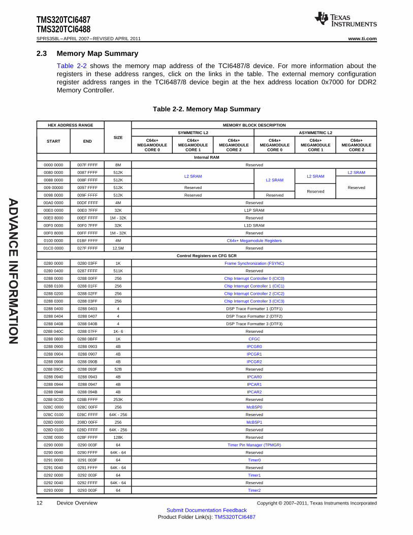
2.3 Memory Map Summary
Table 2-2 shows the memory map address of the TCI6487/8 device. For more information about theregisters in these address ranges, click on the links in the table. The external memory configurationregister address ranges in the TCI6487/8 device begin at the hex address location 0x7000 for DDR2Memory Controller.
Table 2-2. Memory Map Summary
HEX ADDRESS RANGE MEMORY BLOCK DESCRIPTION
SYMMETRIC L2 ASYMMETRIC L2SIZE
C64x+ C64x+ C64x+ C64x+ C64x+ C64x+START ENDMEGAMODULE MEGAMODULE MEGAMODULE MEGAMODULE MEGAMODULE MEGAMODULE
CORE 0 CORE 1 CORE 2 CORE 0 CORE 1 CORE 2
Internal RAM
0000 0000 007F FFFF 8M Reserved
0080 0000 0087 FFFF 512K L2 SRAML2 SRAM L2 SRAM
0088 0000 008F FFFF 512K L2 SRAM
009 00000 0097 FFFF 512K Reserved ReservedReserved
0098 0000 009F FFFF 512K Reserved Reserved
00A0 0000 00DF FFFF 4M Reserved
00E0 0000 00E0 7FFF 32K L1P SRAM
00E0 8000 00EF FFFF 1M - 32K Reserved
00F0 0000 00F0 7FFF 32K L1D SRAM
00F0 8000 00FF FFFF 1M - 32K Reserved
0100 0000 01BF FFFF 4M C64x+ Megamodule Registers
01C0 0000 027F FFFF 12.5M Reserved
Control Registers on CFG SCR
0280 0000 0280 03FF 1K Frame Synchronization (FSYNC)
0280 0400 0287 FFFF 511K Reserved
0288 0000 0288 00FF 256 Chip Interrupt Controller 0 (CIC0)
0288 0100 0288 01FF 256 Chip Interrupt Controller 1 (CIC1)
0288 0200 0288 02FF 256 Chip Interrupt Controller 2 (CIC2)
0288 0300 0288 03FF 256 Chip Interrupt Controller 3 (CIC3)
0288 0400 0288 0403 4 DSP Trace Formatter 1 (DTF1)
0288 0404 0288 0407 4 DSP Trace Formatter 2 (DTF2)
0288 0408 0288 040B 4 DSP Trace Formatter 3 (DTF3)
0288 040C 0288 07FF 1K- 6 Reserved
0288 0800 0288 0BFF 1K CFGC
0288 0900 0288 0903 4B IPCGR0
0288 0904 0288 0907 4B IPCGR1
0288 0908 0288 090B 4B IPCGR2
0288 090C 0288 093F 52B Reserved
0288 0940 0288 0943 4B IPCAR0
0288 0944 0288 0947 4B IPCAR1
0288 0948 0288 094B 4B IPCAR2
0288 0C00 028B FFFF 253K Reserved
028C 0000 028C 00FF 256 McBSP0
028C 0100 028C FFFF 64K - 256 Reserved
028D 0000 208D 00FF 256 McBSP1
028D 0100 028D FFFF 64K - 256 Reserved
028E 0000 028F FFFF 128K Reserved
0290 0000 0290 003F 64 Timer Pin Manager (TPMGR)
0290 0040 0290 FFFF 64K - 64 Reserved
0291 0000 0291 003F 64 Timer0
0291 0040 0291 FFFF 64K - 64 Reserved
0292 0000 0292 003F 64 Timer1
0292 0040 0292 FFFF 64K - 64 Reserved
0293 0000 0293 003F 64 Timer2
12 Device Overview Copyright © 2007–2011, Texas Instruments Incorporated
Submit Documentation FeedbackProduct Folder Link(s): TMS320TCI6487
AD
VA
NC
E I
NF
OR
MA
TIO
N
TMS320TCI6487TMS320TCI6488
www.ti.com SPRS358L–APRIL 2007–REVISED APRIL 2011
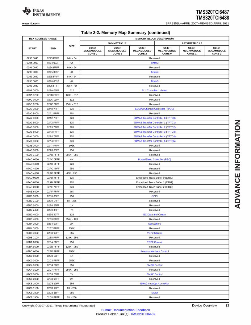
Table 2-2. Memory Map Summary (continued)HEX ADDRESS RANGE MEMORY BLOCK DESCRIPTION
SYMMETRIC L2 ASYMMETRIC L2SIZE
C64x+ C64x+ C64x+ C64x+ C64x+ C64x+START ENDMEGAMODULE MEGAMODULE MEGAMODULE MEGAMODULE MEGAMODULE MEGAMODULE
CORE 0 CORE 1 CORE 2 CORE 0 CORE 1 CORE 2
0293 0040 0293 FFFF 64K - 64 Reserved
0294 0000 0294 003F 64 Timer3
0294 0040 0294 FFFF 64K - 64 Reserved
0295 0000 0295 003F 64 Timer4
0295 0040 0295 FFFF 64K - 64 Reserved
0296 0000 0296 003F 64 Timer5
0296 0040 0296 FFFF 256K - 64 Reserved
029A 0000 029A 01FF 512 PLL Controller 1 (Main)
029A 0200 029B FFFF 128K - 512 Reserved
029C 0000 029C 01FF 512 Reserved
029C 0200 029C 02FF 256K - 512 Reserved
02A0 0000 02A0 7FFF 32K EDMA3 Channel Controller (TPCC)
02A0 8000 02A1 FFFF 96K Reserved
02A2 0000 02A2 7FFF 32K EDMA3 Transfer Controller 0 (TPTC0)
02A2 8000 02A2 FFFF 32K EDMA3 Transfer Controller 1 (TPTC1)
02A3 0000 02A3 7FFF 32K EDMA3 Transfer Controller 2 (TPTC2)
02A3 8000 02A3 FFFF 32K EDMA3 Transfer Controller 3 (TPTC3)
02A4 0000 02A4 7FFF 32K EDMA3 Transfer Controller 4 (TPTC4)
02A4 8000 02A4 FFFF 32K EDMA3 Transfer Controller 5 (TPTC5)
02A5 0000 02A7 FFFF 192K Reserved
02A8 0000 02A8 00FF 256 Reserved
02A8 0100 02AB FFFF 256K - 256 Reserved
02AC 0000 02AC 0FFF 4K Power/Sleep Controller (PSC)
02AC 1000 02AC 3FFF 12K Reserved
02AC 4000 02AC 40FF 256 Reserved
02AC 4100 02AC FFFF 48K - 256 Reserved
02AD 0000 02AD 7FFF 32K Embedded Trace Buffer 0 (ETB0)
02AD 8000 02AD FFFF 32K Embedded Trace Buffer 1 (ETB1)
02AE 0000 02AE 7FFF 32K Embedded Trace Buffer 2 (ETB2)
02AE 8000 02AF FFFF 96K Reserved
02B0 0000 02B0 00FF 256 GPIO
02B0 0100 02B0 1FFF 8K - 256 Reserved
02B0 2000 02B0 23FF 1K Reserved
02B0 2400 02B0 3FFF 7K Reserved
02B0 4000 02B0 407F 128 I2C Data and Control
02B0 4080 02B3 FFFF 256K - 128 Reserved
02B4 0000 02B4 07FF 2K Semaphore
02B4 0800 02B7 FFFF 254K Reserved
02B8 0000 02B8 00FF 256 VCP2 Control
02B8 0100 02B8 FFFF 128K - 256 Reserved
02BA 0000 02BA 00FF 256 TCP2 Control
02BA 0100 02BB FFFF 128K - 256 Reserved
02BC 0000 02BF FFFF 256K Antenna Interface Control
02C0 0000 02C0 03FF 1K Reserved
02C0 0400 02C3 FFFF 255K Reserved
02C4 0000 02C4 00FF 256 SMGII Control
02C4 0100 02C7 FFFF 256K - 256 Reserved
02C8 0000 02C8 07FF 2K EMAC Control
02C8 0800 02C8 0FFF 2K Reserved
02C8 1000 02C8 10FF 256 EMAC Interrupt Controller
02C8 1100 02C8 17FF 2K - 256 Reserved
02C8 1800 02C8 18FF 256 MDIO
02C8 1900 02C8 FFFF 2K - 256 Reserved
Copyright © 2007–2011, Texas Instruments Incorporated Device Overview 13Submit Documentation Feedback
Product Folder Link(s): TMS320TCI6487
AD
VA
NC
E IN
FO
RM
AT
ION
TMS320TCI6487TMS320TCI6488SPRS358L–APRIL 2007–REVISED APRIL 2011 www.ti.com
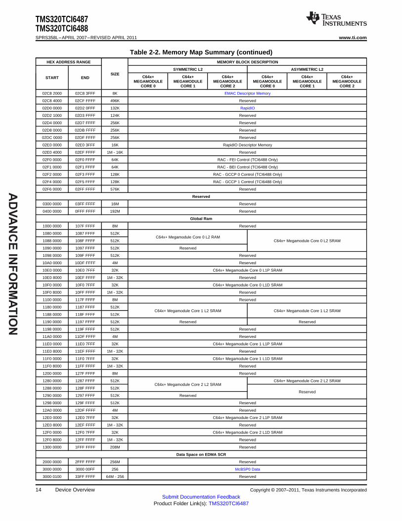
Table 2-2. Memory Map Summary (continued)HEX ADDRESS RANGE MEMORY BLOCK DESCRIPTION
SYMMETRIC L2 ASYMMETRIC L2SIZE
C64x+ C64x+ C64x+ C64x+ C64x+ C64x+START ENDMEGAMODULE MEGAMODULE MEGAMODULE MEGAMODULE MEGAMODULE MEGAMODULE
CORE 0 CORE 1 CORE 2 CORE 0 CORE 1 CORE 2
02C8 2000 02C8 3FFF 8K EMAC Descriptor Memory
02C8 4000 02CF FFFF 496K Reserved
02D0 0000 02D2 0FFF 132K RapidIO
02D2 1000 02D3 FFFF 124K Reserved
02D4 0000 02D7 FFFF 256K Reserved
02D8 0000 02DB FFFF 256K Reserved
02DC 0000 02DF FFFF 256K Reserved
02E0 0000 02E0 3FFF 16K RapidIO Descriptor Memory
02E0 4000 02EF FFFF 1M - 16K Reserved
02F0 0000 02F0 FFFF 64K RAC - FEI Control (TCI6488 Only)
02F1 0000 02F1 FFFF 64K RAC - BEI Control (TCI6488 Only)
02F2 0000 02F3 FFFF 128K RAC - GCCP 0 Control (TCI6488 Only)
02F4 0000 02F5 FFFF 128K RAC - GCCP 1 Control (TCI6488 Only)
02F6 0000 02FF FFFF 576K Reserved
Reserved
0300 0000 03FF FFFF 16M Reserved
0400 0000 0FFF FFFF 192M Reserved
Global Ram
1000 0000 107F FFFF 8M Reserved
1080 0000 1087 FFFF 512KC64x+ Megamodule Core 0 L2 RAM
1088 0000 108F FFFF 512K C64x+ Megamodule Core 0 L2 SRAM
1090 0000 1097 FFFF 512K Reserved
1098 0000 109F FFFF 512K Reserved
10A0 0000 10DF FFFF 4M Reserved
10E0 0000 10E0 7FFF 32K C64x+ Megamodule Core 0 L1P SRAM
10E0 8000 10EF FFFF 1M - 32K Reserved
10F0 0000 10F0 7FFF 32K C64x+ Megamodule Core 0 L1D SRAM
10F0 8000 10FF FFFF 1M - 32K Reserved
1100 0000 117F FFFF 8M Reserved
1180 0000 1187 FFFF 512KC64x+ Megamodule Core 1 L2 SRAM C64x+ Megamodule Core 1 L2 SRAM
1188 0000 118F FFFF 512K
1190 0000 1197 FFFF 512K Reserved Reserved
1198 0000 119F FFFF 512K Reserved
11A0 0000 11DF FFFF 4M Reserved
11E0 0000 11E0 7FFF 32K C64x+ Megamodule Core 1 L1P SRAM
11E0 8000 11EF FFFF 1M - 32K Reserved
11F0 0000 11F0 7FFF 32K C64x+ Megamodule Core 1 L1D SRAM
11F0 8000 11FF FFFF 1M - 32K Reserved
1200 0000 127F FFFF 8M Reserved
1280 0000 1287 FFFF 512K C64x+ Megamodule Core 2 L2 SRAMC64x+ Megamodule Core 2 L2 SRAM
1288 0000 128F FFFF 512KReserved
1290 0000 1297 FFFF 512K Reserved
1298 0000 129F FFFF 512K Reserved
12A0 0000 12DF FFFF 4M Reserved
12E0 0000 12E0 7FFF 32K C64x+ Megamodule Core 2 L1P SRAM
12E0 8000 12EF FFFF 1M - 32K Reserved
12F0 0000 12F0 7FFF 32K C64x+ Megamodule Core 2 L1D SRAM
12F0 8000 12FF FFFF 1M - 32K Reserved
1300 0000 1FFF FFFF 208M Reserved
Data Space on EDMA SCR
2000 0000 2FFF FFFF 256M Reserved
3000 0000 3000 00FF 256 McBSP0 Data
3000 0100 33FF FFFF 64M - 256 Reserved
14 Device Overview Copyright © 2007–2011, Texas Instruments Incorporated
Submit Documentation FeedbackProduct Folder Link(s): TMS320TCI6487
AD
VA
NC
E I
NF
OR
MA
TIO
N
TMS320TCI6487TMS320TCI6488
www.ti.com SPRS358L–APRIL 2007–REVISED APRIL 2011
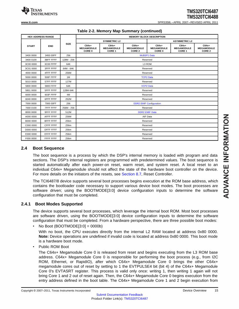
Table 2-2. Memory Map Summary (continued)HEX ADDRESS RANGE MEMORY BLOCK DESCRIPTION
SYMMETRIC L2 ASYMMETRIC L2SIZE
C64x+ C64x+ C64x+ C64x+ C64x+ C64x+START ENDMEGAMODULE MEGAMODULE MEGAMODULE MEGAMODULE MEGAMODULE MEGAMODULE
CORE 0 CORE 1 CORE 2 CORE 0 CORE 1 CORE 2
3400 0000 3400 00FF 256 McBSP1 Data
3400 0100 3BFF FFFF 128M - 256 Reserved
3C00 0000 3C00 FFFF 64K L3 ROM
3C01 0000 3FFF FFFF 64M - 64K Reserved
4000 0000 4FFF FFFF 256M Reserved
5000 0000 500F FFFF 1M TCP2 Data
5010 0000 57FF FFFF 127M Reserved
5800 0000 5800 FFFF 64K VCP2 Data
5801 0000 5FFF FFFF 128M 64K Reserved
6000 0000 603F FFFF 4M Reserved
6040 0000 6FFF FFFF 252M Reserved
7000 0000 7000 00FF 256 DDR2 EMIF Configuration
7000 0100 7FFF FFFF 256M - 256 Reserved
8000 0000 9FFF FFFF 512M DDR2 EMIF Data
A000 0000 AFFF FFFF 256M AIF Data
B000 0000 BFFF FFFF 256m Reserved
C000 0000 CFFF FFFF 256m Reserved
D000 0000 DFFF FFFF 256m Reserved
E000 0000 EFFF FFFF 256m Reserved
F000 0000 FFFF FFFF 256m Reserved
2.4 Boot Sequence
The boot sequence is a process by which the DSP's internal memory is loaded with program and datasections. The DSP's internal registers are programmed with predetermined values. The boot sequence isstarted automatically after each power-on reset, warm reset, and system reset. A local reset to anindividual C64x+ Megamodule should not affect the state of the hardware boot controller on the device.For more details on the initiators of the resets, see Section 8.7, Reset Controller.
The TCI6487/8 device supports several boot processes begins execution at the ROM base address, whichcontains the bootloader code necessary to support various device boot modes. The boot processes aresoftware driven; using the BOOTMODE[3:0] device configuration inputs to determine the softwareconfiguration that must be completed.
2.4.1 Boot Modes Supported
The device supports several boot processes, which leverage the internal boot ROM. Most boot processesare software driven, using the BOOTMODE[3:0] device configuration inputs to determine the softwareconfiguration that must be completed. From a hardware perspective, there are three possible boot modes:• No Boot (BOOTMODE[3:0] = 0000b)
With no boot, the CPU executes directly from the internal L2 RAM located at address 0x80 0000.Note: Device operations are undefined if invalid code is located at address 0x80 0000. This boot modeis a hardware boot mode.
• Public ROM BootThe C64x+ Megamodule Core 0 is released from reset and begins executing from the L3 ROM baseaddress. C64x+ Megamodule Core 0 is responsible for performing the boot process (e.g., from I2CROM, Ethernet, or RapidIO), after which C64x+ Megamodule Core 0 brings the other C64x+megamodule cores out of reset by setting to 1 the EVTPULSE4 bit (bit 4) of the C64x+ MegamoduleCore 0's EVTASRT register. This process is valid only once: writing 1, then writing 1 again will notbring Core 1 and 2 out of reset again. Then, the C64x+ Megamodule Core 0 begins execution from theentry address defined in the boot table. The C64x+ Megamodule Core 1 and 2 begin execution from
Copyright © 2007–2011, Texas Instruments Incorporated Device Overview 15Submit Documentation Feedback
Product Folder Link(s): TMS320TCI6487

AD
VA
NC
E IN
FO
RM
AT
ION
TMS320TCI6487TMS320TCI6488SPRS358L–APRIL 2007–REVISED APRIL 2011 www.ti.com
their L2 RAMs' base address.
The boot process performed by C64x+ Megamodule Core 0 in public ROM boot is determined by theBOOTMODE[3:0] value in the DEVSTAT register. C64x+ Megamodule Core 0 reads this value, and thenexecutes the associated boot process in software.
16 Device Overview Copyright © 2007–2011, Texas Instruments Incorporated
Submit Documentation FeedbackProduct Folder Link(s): TMS320TCI6487

AD
VA
NC
E I
NF
OR
MA
TIO
N
TMS320TCI6487TMS320TCI6488
www.ti.com SPRS358L–APRIL 2007–REVISED APRIL 2011
Table 2-3. TCI6487/8 Supported Boot Modes
MODE NAME BOOTMODE[3:0] DESCRIPTION
No Boot 0000b No Boot (BOOTMODE[3:0] = 0000b)
I2C Master Boot A 0001b Slave I2C address is 0x50. C64x+ Megamodule Core 0 configures I2C, acts as amaster to the I2C bus and copies data from an I2C EEPROM or a device acting as anI2C slave to the DSP using a predefined boot table format. The destination addressand length are contained within the boot table. After boot table copy is complete, theC64x+ Megamodule Core 0 brings the other C64x+ Megamodule Cores out of resetby setting to 1 the EVTPULSE4 bit (bit 4) of the C64x+ Megamodule Core EVTASRTregister.
I2C Master Boot B 0010b Similar to I2C boot A except the slave I2C address is 0x51.
I2C Slave Boot 0011 The C64x+ Megamodule Core 0 configures I2C and acts as a slave and will acceptdata and code section packets through the I2C interface. It is required that an I2Cmaster in present in the system.
EMAC Master Boot 0100b TI Ethernet Boot, C64x+ Megamodule Core 0 configures EMAC0 and EDMA, ifrequired, and brings the code image into the internal on-chip memory via the protocolEMAC Slave Boot 0101bdefined by the boot method (EMAC bootloader). After initializing the on-chip memory
EMAC Forced-Mode Boot 0110b to the known state, C64x+ Megamodule Core 0 brings the other C64x+ MegamoduleCores out of reset.
Reserved 0111b Reserved
Serial RapidIO Boot (Config 0) 1000b The C64x+ Megamodule Core 0 configures the SRIO and an external host loads theapplication via SRIO peripheral, using directIO protocol. A doorbell interrupt is used toSerial RapidIO Boot (Config 1) 1001bindicate that the code has been loaded. For more details on the Serial RapidIO
Serial RapidIO Boot (Config 2) 1010b configurations, see Table 2-4.
Serial RapidIO Boot (Config 3) 1011b
C64x+ Megamodule Core 0 configures Serial RapidIO and EDMA, if required, and brings the code imageinto the internal on-chip memory via the protocol defined by the boot method (SRIO bootloader) and thenC64x+ Megamodule Core 0 brings the other C64x+ Megamodule Cores out of reset. Note that SRIO bootmodes are only supported on port 0.
Table 2-4. Serial RapidIO (SRIO) Supported Boot Modes
SRIO BOOT MODE SERDES CLOCK LINK RATE BOOTMODE[3:0]
Bootmode 8 - Config 0 125 MHz 1.25 Gbps 1000b
Bootmode 9 - Config 1 125 MHz 3.125 Gbps 1001b
Bootmode 10 - Config 2 156.25 MHz 1.25 Gbps 1010b
Bootmode 11 - Config 3 156.25 MHz 3.125 Gbps 1011b
All the other BOOTMODE[3:0] modes are reserved.
2.4.2 Second-Level Bootloaders
Any of the boot modes can be used to download a second-level bootloader. A second-level bootloaderallows for any level of customization to current boot methods as well as the definition of a completelycustomized boot.
Copyright © 2007–2011, Texas Instruments Incorporated Device Overview 17Submit Documentation Feedback
Product Folder Link(s): TMS320TCI6487

AD
VA
NC
E IN
FO
RM
AT
ION
AE
AD
AC
AB
AA
Y
W
V
U
T
R
13121110987654321
13121110987654321
AF
AG
14
14
AE
AD
AC
AB
AA
Y
W
V
U
T
R
AF
AGRSV04 AIF_VDDT11 VSS AIFTXN4 AIFTXP4
ALTCORECLKN
VSS AIFRXN5 AIFRXP5 VSS
VSS AIF_VDDT11 AIF_VDDA11 VSS AIF_VDDT11
SYSCLKN VSS VSS AIFRXP4 AIFRXN4
FRAMEBURSTN
VSS AIFTXP5 AIFTXN5 RSV02
DVDD18 VSS VSS VSS VSS CVDDMON DVDD18MON
ALTFSYNCCLK
CORECLKSEL
ALTFSYNCPULSE
RSV06
SYSCLKOUT
FSYNCCLKP
VSS DVDD18
DVDD18 AVDD118
VSSALTCORE
CLKP
RSV07 SYSCLKP
VSS VSS VSS RESETSTAT DVDD18
VSS VSS VSS RSV23 POR
VSS VSS TRTSMFRAME
CLKXWRST
DVDD18 VSS GP15 TRTCLK DVDD18
GP12 GP11VSS GP13 VSS
VSSGP14GP10 DVDD18
VSSVSSGP08GP07DVDD18
CVDD VSS CVDD VSS CVDD VSS
FSYNCCLKN
FRAMEBURSTP
VSS DVDD18
TMS
GP02
TRST TDO TCK DVDD18
GP05 GP06 TDI VSSVSS CVDD VSS CVDD VSS CVDD
EMU10
DVDD18
EMU15
VSS GP03 GP01 DVDD18
DVDD18
GP04
EMU00
VSS
EMU01 EMU07
EMU11 GP00
GP09
CVDD VSS CVDD VSS CVDD VSS
VSS CVDD VSS CVDD VSS CVDD
CVDD VSS CVDD VSS CVDD VSS
TMS320TCI6487TMS320TCI6488SPRS358L–APRIL 2007–REVISED APRIL 2011 www.ti.com
2.5 Pin Assignments
2.5.1 Pin Map
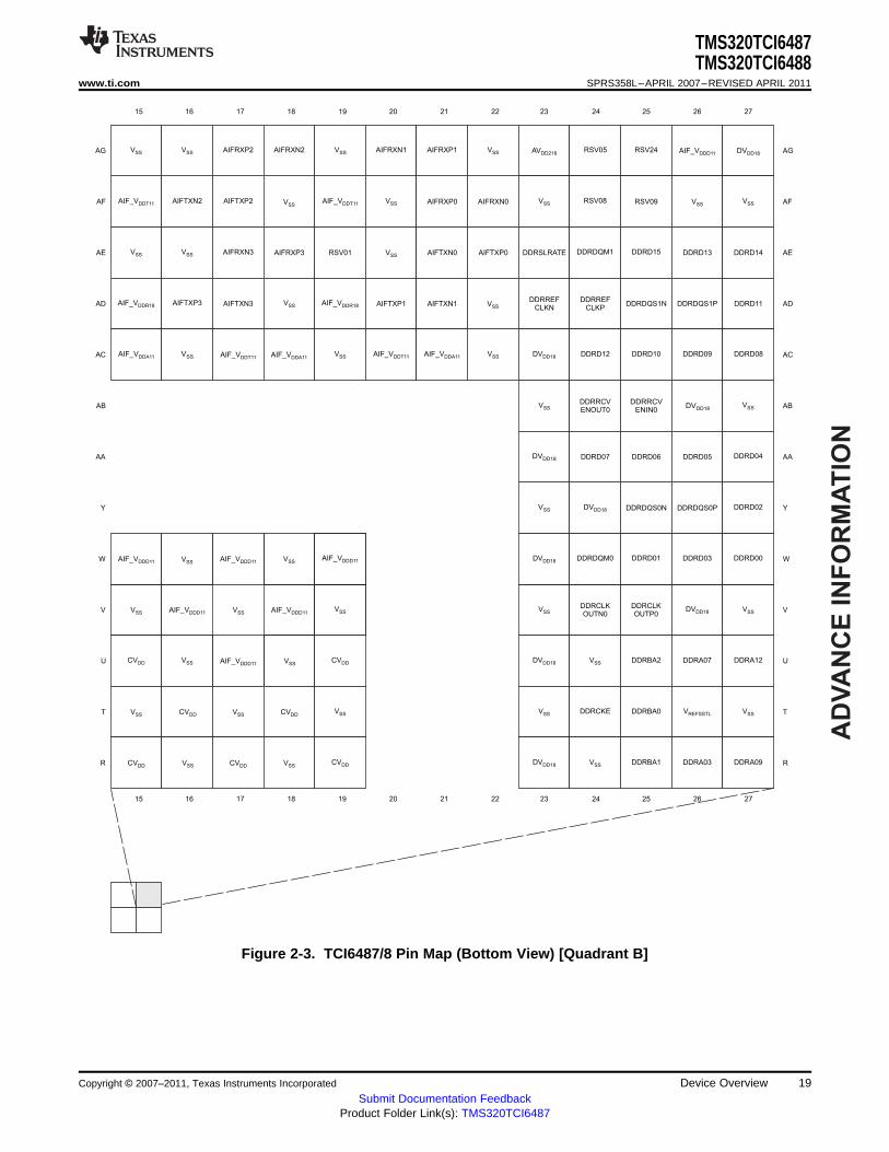
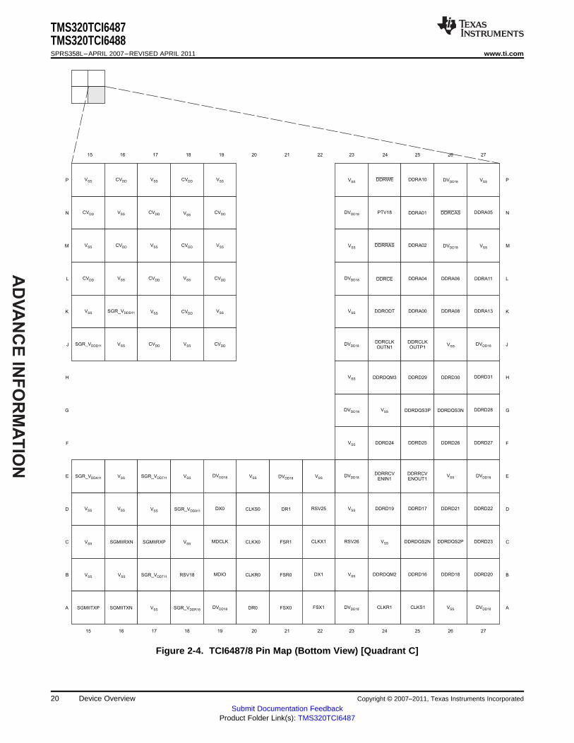
Figure 2-2 through Figure 2-5 show the TCI6487/8 pin assignments in four quadrants (A, B, C, and D).
Figure 2-2. TCI6487/8 Pin Map (Bottom View) [Quadrant A]
18 Device Overview Copyright © 2007–2011, Texas Instruments Incorporated
Submit Documentation FeedbackProduct Folder Link(s): TMS320TCI6487
AD
VA
NC
E I
NF
OR
MA
TIO
N
AE
AD
AC
AB
AA
Y
W
V
U
T
R
262524232221201918171615
262524232221201918171615
AF
AG
27
27
AE
AD
AC
AB
AA
Y
W
V
U
T
R
AF
AGAVDD218RSV05 RSV24 AIF_VDDD11 DVDD18
VSS RSV08 RSV09 VSSVSS
DVDD18 DDRD12 DDRD10 DDRD08
DDRSLRATE DDRDQM1 DDRD15 DDRD13 DDRD14
DDRREFCLKN
DDRREFCLKP
DDRDQS1N DDRDQS1P DDRD11
VSS VSS AIFRXP2 AIFRXN2 VSS AIFRXN1
AIF_VDDT11 AIFRXP0
RSV01 VSS
AIFTXP1
VSS AIF_VDDT11
AIFRXP1 VSS
VSS AIFRXN0
AIFTXN0 AIFTXP0
AIF_VDDT11 AIFTXN2 AIFTXP2 VSS
VSS VSS AIFRXN3 AIFRXP3
AIF_VDDR18 AIFTXP3 AIFTXN3 VSS
AIF_VDDA11 VSS AIF_VDDT11 AIF_VDDA11
DDRRCVENIN0
DVDD18VSS
DDRRCVENOUT0
VSS
DVDD18 DDRD05DDRD06 DDRD04
DDRD02VSS DDRDQS0PDDRDQS0NDVDD18
DVDD18 DDRDQM0 DDRD01 DDRD03 DDRD00
AIFTXN1 VSS
AIF_VDDA11 VSS
AIF_VDDD11
VSS
VSSAIF_VDDD11 VSS
AIF_VDDD11
AIF_VDDD11 VSS AIF_VDDD11VSS VSS
DDRCLKOUTN0
DDRCLKOUTP0
DVDD18 VSS
CVDD
CVDD
VSS
VSS AIF_VDDD11 VSSCVDD
CVDD
CVDD
VSS
VSS
VSS CVDD
CVDD VSS
DDRD07
DVDD18 VSS DDRBA2 DDRA07 DDRA12
VSS DDRCKE DDRBA0 VREFSSTL VSS
DVDD18 VSS DDRBA1 DDRA03 DDRA09
DDRD09
AIF_VDDR18
TMS320TCI6487TMS320TCI6488
www.ti.com SPRS358L–APRIL 2007–REVISED APRIL 2011
Figure 2-3. TCI6487/8 Pin Map (Bottom View) [Quadrant B]
Copyright © 2007–2011, Texas Instruments Incorporated Device Overview 19Submit Documentation Feedback
Product Folder Link(s): TMS320TCI6487
AD
VA
NC
E IN
FO
RM
AT
ION
M
L
K
J
H
G
F
E
D
C
B
262524232221201918171615
N
P
27
M
L
K
J
H
G
F
E
D
C
B
N
PVSSDDRWE DDRA10 DVDD18 VSS
DVDD18 PTV18 DDRA01 DDRCAS DDRA05
VSS DDRODT DDRA00 DDRA13
VSSDDRRAS DDRA02 DVDD18 VSS
DVDD18 DDRCE DDRA04 DDRA06 DDRA11
VSS CVDD VSS CVDD VSS
CVDD
VSS
CVDD VSS CVDD VSS
VSS SGR_VDDD11 VSS CVDD
DDRCLKOUTP1
VSSDVDD18
DDRCLKOUTN1
DVDD18
VSS DDRD30DDRD29 DDRD31
DDRD28DVDD18 DDRDQS3NDDRDQS3PVSS
VSS DDRD24 DDRD25 DDRD26 DDRD27
VSSSGR_VDDA11 DVDD18VSSVSS SGR_VDDT11 VSS
DVDD18 DVDD18DDRRCV
ENIN1DDRRCVENOUT1
VSS DVDD18
VSS
VSS
VSS
VSS VSS SGR_VDDA11DX0
MDIO
VSS
RSV18
MDCLK
VSS SGR_VDDT11
SGMIIRXN SGMIIRXP
DDRDQM3
VSS DDRD19 DDRD17 DDRD21 DDRD22
RSV26 VSS DDRDQS2N DDRDQS2P DDRD23
VSS DDRDQM2 DDRD16 DDRD18 DDRD20
DDRA08
CVDDSGR_VDDD11 VSS CVDD VSS
VSS CVDD VSS CVDD VSS
CVDDCVDD VSS CVDD VSS
A
262524232221201918171615 27
ASGMIITXP DVDD18SGR_VDDR18SGMIITXN VSSDVDD18 CLKR1 CLKS1 VSS DVDD18
CLKS0 DR1 RSV25
DX1
FSR1
FSR0
CLKX1
CLKR0
CLKX0
FSX1FSX0DR0
TMS320TCI6487TMS320TCI6488SPRS358L–APRIL 2007–REVISED APRIL 2011 www.ti.com
Figure 2-4. TCI6487/8 Pin Map (Bottom View) [Quadrant C]
20 Device Overview Copyright © 2007–2011, Texas Instruments Incorporated
Submit Documentation FeedbackProduct Folder Link(s): TMS320TCI6487

AD
VA
NC
E I
NF
OR
MA
TIO
N
M
L
K
J
H
G
F
E
D
C
B
121110987654321
N
P
13
H
G
F
E
D
C
B
VSS DVDD18 EMU16 EMU13 VSS
DVDD18
VSS
EMU03 EMU09 EMU02 EMU06
RSV12 EMU14 RSV11 RSV10
VSS VCNTL2VCNTL3 VSS
DVDD18VSS RSV13VCNTL0VCNTL1
VSS TIMO0 RSV14 TIMO1 VSS
RSV21DVDD18 RSV22 VSSVSS TIMI0 SCL DVDD18 SGR_VDDT11 VSS SGR_VDDA11 VSS SGR_VDDT11
VSS
VSS
VSS
VSS VSS SDA RSV27
VSS
TIMI1
VSS
RSV28
VSS VSS
VSS VSS
DVDD18
RIOSGMIICLKN
VSS VSS SGR_VDDA11 VSS
RIOSGMIICLKP
RIOTXP0 RIOTXN0 SGR_VDDR18 RIOTXN1
VSS VSS VSS RSV17 SGR_VDDT11
DVDD18NMI2 NMI1 RSV29 NMI0
EMU05 EMU04 EMU18 EMU08 VSS
DVDD18DVDD18 VSS EMU12 EMU17
A
121110987654321 13
ADVDD18DVDD18VSSVSS VSS
RIORXN0 RIORXP0 VSS RIORXP1 RIORXN1
RSV19 RSV15 VSS
SGR_VDDT11
RSV16
VSS
VSS
VSS
RSV20
VSSVSSVSS
14
M
L
K
N
P
J
VSS CVDD VSS CVDD VSS
CVDD
VSS
CVDD VSS CVDD VSS
VSS CVDD VSS SGR_VDDD11
SGR_VDDD11VSS CVDD VSS
VSS CVDD VSS CVDD VSS
CVDDCVDD VSS CVDD VSS
CVDD
CVDD
VSS
SGR_VDDD11
VSS
CVDD
VSS
VSS
VSS
RIOTXP1
VSS
14
VSS
TMS320TCI6487TMS320TCI6488
www.ti.com SPRS358L–APRIL 2007–REVISED APRIL 2011
Figure 2-5. TCI6487/8 Pin Map (Bottom View) [Quadrant D]
Copyright © 2007–2011, Texas Instruments Incorporated Device Overview 21Submit Documentation Feedback
Product Folder Link(s): TMS320TCI6487
AD
VA
NC
E IN
FO
RM
AT
ION
Reset andInterrupts
IEEE Standard1149.1(JTAG)
Emulation
Reserved
AVDD218
TMS
RESETSTAT
RSV
Control/Status
SYSCLKPSYSCLKN
SYSCLKOUT
CORECLKSEL
ALTCORECLKP
ALTCORECLKN
Clock/PLL1and
PLL Controller
Clock/PLL2
TDO
TDI
TCK
TRST
·
EMU00
EMU01
EMU02
·
·
EMU14
EMU15
EMU16
EMU17
EMU18
RESET
NMI0
NMI1
NMI2
XWRST
AVDD118
TMS320TCI6487TMS320TCI6488SPRS358L–APRIL 2007–REVISED APRIL 2011 www.ti.com
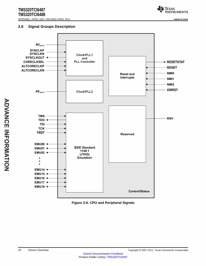
2.6 Signal Groups Description
Figure 2-6. CPU and Peripheral Signals
22 Device Overview Copyright © 2007–2011, Texas Instruments Incorporated
Submit Documentation FeedbackProduct Folder Link(s): TMS320TCI6487

AD
VA
NC
E I
NF
OR
MA
TIO
N
DDRD[31:0]
DDRCE
DDRA[13:0]14
DDRDQM0
DDRDQM1
DDRDQM2
DDRDQM3
Data
Memory Map
Address
Byte Enables
DDRCLKOUTP
DDRCLKOUTN
DDRCAS
DDRRAS
DDRWE
DDRDQSP[3:0]
DDRDQSN[3:0]
DDRRCVENIN[2:0]
DDRRCVENOUT[2:0]
DDRODT
DDRSLRATE
VREFSSTL
DDRBA0
DDRBA1
DDRBA2
ExternalMemory
Controller
Bank Address
DDR Memory Controller (32-bit Data Bus)
32
TMS320TCI6487TMS320TCI6488
www.ti.com SPRS358L–APRIL 2007–REVISED APRIL 2011
Figure 2-7. DDR Memory Controller Peripheral Signals
Copyright © 2007–2011, Texas Instruments Incorporated Device Overview 23Submit Documentation Feedback
Product Folder Link(s): TMS320TCI6487
AD
VA
NC
E IN
FO
RM
AT
ION
TIMI0
TIMO0
GP00
GP01
GP02
GP03
GP04
GP05
GP06
GP07
RIOTXN0
RIOTXP0
RIOTXN1
RIOTXP1
RIORXN0
RIORXP0
RIORXN1
RIORXP1
Transmit
Receive
Clock
RapidIO
RIOSGMIICLKP(A)
RIOSGMIICLKN(A)
GP08
GP09
GP10
GP11
GP12
GP13
GP14
GP15
GPIO
General-Purpose Input/Output 0 (GPIO) Port
TIMO1
TIMI1Timer Pin Manager
Timers (64-Bit)
TMS320TCI6487TMS320TCI6488SPRS358L–APRIL 2007–REVISED APRIL 2011 www.ti.com
A. Reference Clock to drive RapidIO and SGMII.
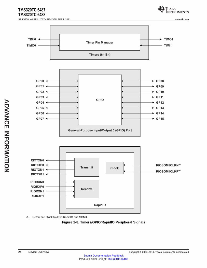
Figure 2-8. Timers/GPIO/RapidIO Peripheral Signals
24 Device Overview Copyright © 2007–2011, Texas Instruments Incorporated
Submit Documentation FeedbackProduct Folder Link(s): TMS320TCI6487
AD
VA
NC
E I
NF
OR
MA
TIO
N
CLKX1
FSX1
DX1
CLKR1
FSR1
DR1
CLKS1
CLKX0
FSX0
DX0
CLKR0
FSR0
DR0
CLKS0
McBSP1
Clock
Receive
Transmit
McBSP0
Clock
Receive
Transmit
Multichannel Buffered Serial Ports(McBSPs)
FRAMEBURSTN
FRAMEBURSTP
ALTFSYNCPULSE
TRT
FSYNCCLKN
FSYNCCLKP
ALTFSYNCCLK
TRTCLK
SMFRAMECLK
FSYNC Clock
Frame Synchroniztion (FSYNC)
AIFTXN[5:0]
AIFTXP[5:0]
AIFRXN[5:0]
AIFRXP[5:0]
SCL
SDA
Transmit
SCL
Receive
Antenna Interface (AIF)
I2C
TMS320TCI6487TMS320TCI6488
www.ti.com SPRS358L–APRIL 2007–REVISED APRIL 2011
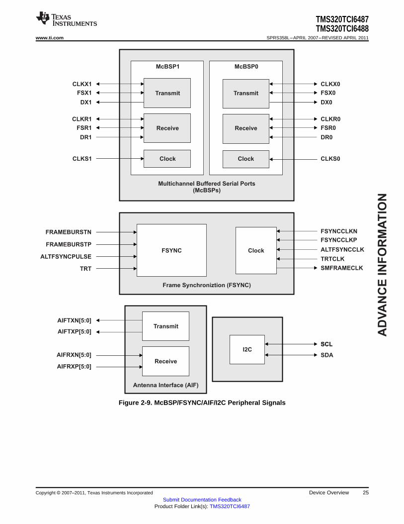
Figure 2-9. McBSP/FSYNC/AIF/I2C Peripheral Signals
Copyright © 2007–2011, Texas Instruments Incorporated Device Overview 25Submit Documentation Feedback
Product Folder Link(s): TMS320TCI6487

AD
VA
NC
E IN
FO
RM
AT
ION
SGMIITXN
SGMIITXP
SGMIIRXN
SGMIIRXP
RIOSGMIICLKN(A)
RIOSGMIICLKP(A)
Ethernet MAC(EMAC)
SGMIITransmit
SGMIIReceive
SGMIIClock
MDIO
Ethernet MAC (EMAC) and MDIO
MDIO
MDCLK
TMS320TCI6487TMS320TCI6488SPRS358L–APRIL 2007–REVISED APRIL 2011 www.ti.com
A. Reference Clock to drive RapidIO and SGMII.
Figure 2-10. EMAC/MDIO [SGMII] Peripheral Signals
26 Device Overview Copyright © 2007–2011, Texas Instruments Incorporated
Submit Documentation FeedbackProduct Folder Link(s): TMS320TCI6487

AD
VA
NC
E I
NF
OR
MA
TIO
N
TMS320TCI6487TMS320TCI6488
www.ti.com SPRS358L–APRIL 2007–REVISED APRIL 2011
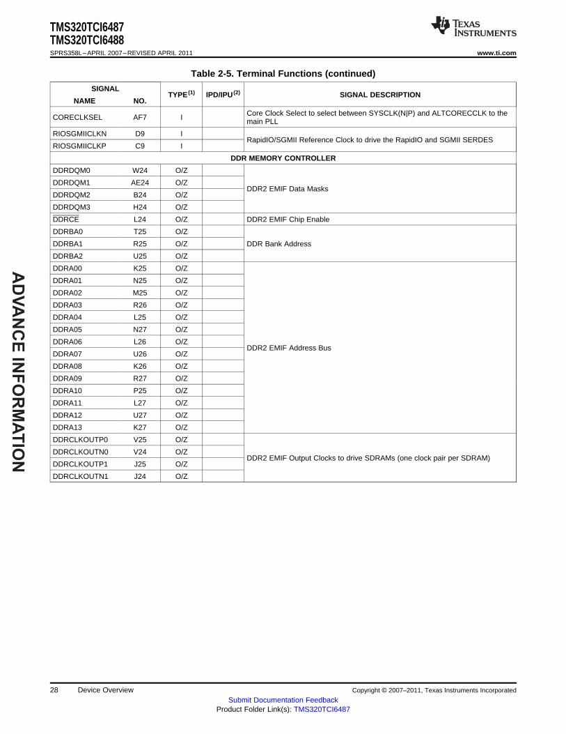
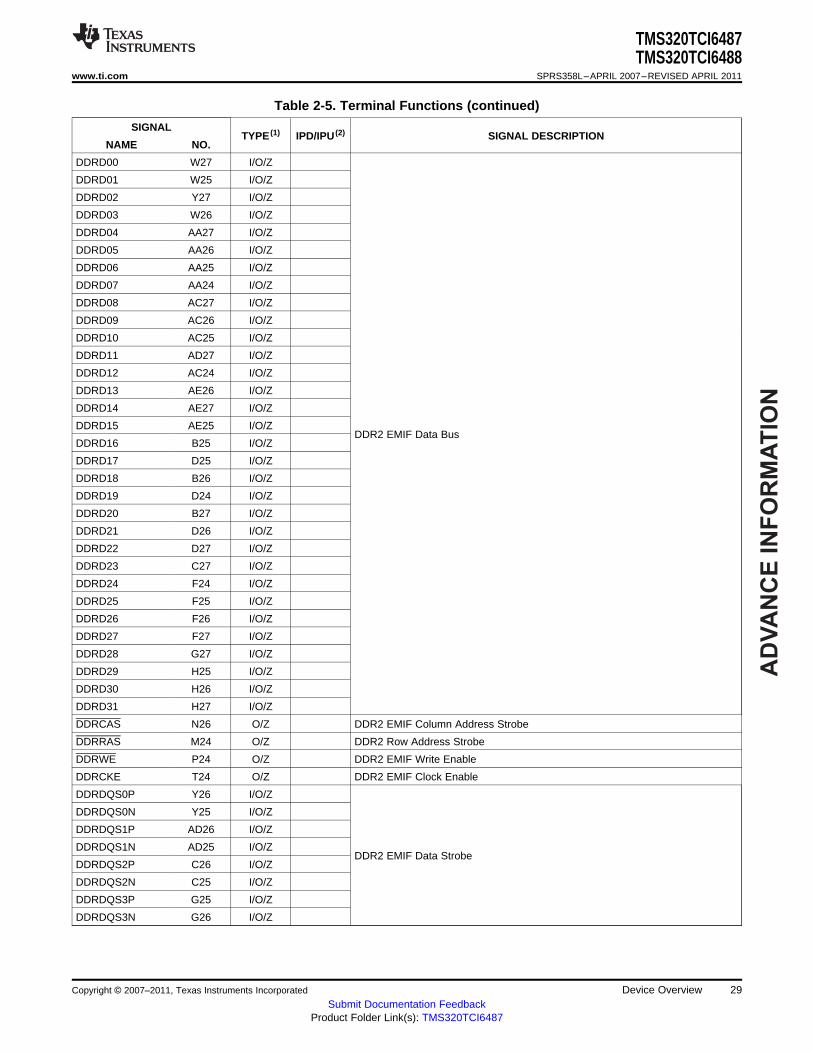
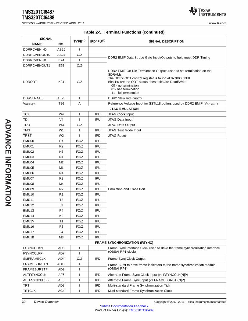
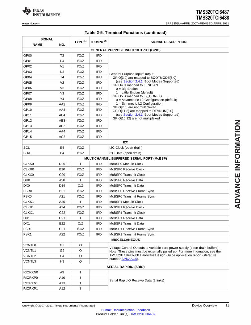
2.7 Terminal Functions
The terminal functions table (Table 2-5) identifies the external signal names, the pin type (I, O, O/Z, orI/O/Z), whether the pin has any internal pullup/pulldown resistors, and the signal function description.
Table 2-5. Terminal Functions
SIGNALTYPE (1) IPD/IPU (2) SIGNAL DESCRIPTION
NAME NO.
ANTENNA INTERFACE
AIFRXN0 AF22 I
AIFRXP0 AF21 I
AIFRXN1 AG20 I
AIFRXP1 AG21 I
AIFRXN2 AG18 I
AIFRXP2 AG17 IAntenna Interface Receive Data (6 links)
AIFRXN3 AE17 I
AIFRXP3 AE18 I
AIFRXN4 AE14 I
AIFRXP4 AE13 I
AIFRXN5 AF12 I
AIFRXP5 AF13 I
AIFTXN0 AE21 O
AIFTXP0 AE22 O
AIFTXN1 AD21 O
AIFTXP1 AD20 O
AIFTXN2 AF16 O
AIFTXP2 AF17 OAntenna Interface Transmit Data (6 links)
AIFTXN3 AD17 O
AIFTXP3 AD16 O
AIFTXN4 AG13 O
AIFTXP4 AG14 O
AIFTXN5 AD13 O
AIFTXP5 AD12 O
CLOCK/RESETS
NMI0 J4 I IPD Non-maskable interrupts. NMI0, NMI1, and NMI2 pins are mapped to C64x+Megamodule Core 0, C64x+ Megamodule Core 1, and C64x+ Megamodule CoreNMI1 J2 I IPD2, respectively. NMIs are edge-driven (rising edge). Any noise on the NMI pin
NMI2 J1 I IPD may trigger an NMI interrupt; therefore, if the NMI pin is not used, it isrecommended that the NMI pin be grounded rather than relying on the IPD.
XWRST AD5 I Warm Reset
RESETSTAT AF4 O Reset Status Output
POR AE5 I Power-on Reset
SYSCLKP AE9 I System Clock Input to Antenna Interface and main PLL (Main PLL optional vsALTCORECLK)SYSCLKN AE10 I
ALTCORECLKN AF10 IAlternate Core Clock Input to main PLL (vs SYSCLK)
ALTCORECLKP AF9 I
DDRREFCLKN AD23 IDDR Reference Clock Input to DDR PLL
DDRREFCLKP AD24 I
System Clock Output to be used as a general purpose output clock for debugSYSCLKOUT AD6 O/Z IPD purposes
(1) I = Input, O = Output, Z = High impedance, S = Supply voltage, GND = Ground, A = Analog signal(2) IPD = internal pulldown, IPU = internal pullup. All internal pullups and pulldowns are 100 μA.
Copyright © 2007–2011, Texas Instruments Incorporated Device Overview 27Submit Documentation Feedback
Product Folder Link(s): TMS320TCI6487
AD
VA
NC
E IN
FO
RM
AT
ION
TMS320TCI6487TMS320TCI6488SPRS358L–APRIL 2007–REVISED APRIL 2011 www.ti.com
Table 2-5. Terminal Functions (continued)
SIGNALTYPE (1) IPD/IPU (2) SIGNAL DESCRIPTION
NAME NO.
Core Clock Select to select between SYSCLK(N|P) and ALTCORECCLK to theCORECLKSEL AF7 I main PLL
RIOSGMIICLKN D9 IRapidIO/SGMII Reference Clock to drive the RapidIO and SGMII SERDES
RIOSGMIICLKP C9 I
DDR MEMORY CONTROLLER
DDRDQM0 W24 O/Z
DDRDQM1 AE24 O/ZDDR2 EMIF Data Masks
DDRDQM2 B24 O/Z
DDRDQM3 H24 O/Z
DDRCE L24 O/Z DDR2 EMIF Chip Enable
DDRBA0 T25 O/Z
DDRBA1 R25 O/Z DDR Bank Address
DDRBA2 U25 O/Z
DDRA00 K25 O/Z
DDRA01 N25 O/Z
DDRA02 M25 O/Z
DDRA03 R26 O/Z
DDRA04 L25 O/Z
DDRA05 N27 O/Z
DDRA06 L26 O/ZDDR2 EMIF Address Bus
DDRA07 U26 O/Z
DDRA08 K26 O/Z
DDRA09 R27 O/Z
DDRA10 P25 O/Z
DDRA11 L27 O/Z
DDRA12 U27 O/Z
DDRA13 K27 O/Z
DDRCLKOUTP0 V25 O/Z
DDRCLKOUTN0 V24 O/ZDDR2 EMIF Output Clocks to drive SDRAMs (one clock pair per SDRAM)
DDRCLKOUTP1 J25 O/Z
DDRCLKOUTN1 J24 O/Z
28 Device Overview Copyright © 2007–2011, Texas Instruments Incorporated
Submit Documentation FeedbackProduct Folder Link(s): TMS320TCI6487
AD
VA
NC
E I
NF
OR
MA
TIO
N
TMS320TCI6487TMS320TCI6488
www.ti.com SPRS358L–APRIL 2007–REVISED APRIL 2011
Table 2-5. Terminal Functions (continued)
SIGNALTYPE (1) IPD/IPU (2) SIGNAL DESCRIPTION
NAME NO.
DDRD00 W27 I/O/Z
DDRD01 W25 I/O/Z
DDRD02 Y27 I/O/Z
DDRD03 W26 I/O/Z
DDRD04 AA27 I/O/Z
DDRD05 AA26 I/O/Z
DDRD06 AA25 I/O/Z
DDRD07 AA24 I/O/Z
DDRD08 AC27 I/O/Z
DDRD09 AC26 I/O/Z
DDRD10 AC25 I/O/Z
DDRD11 AD27 I/O/Z
DDRD12 AC24 I/O/Z
DDRD13 AE26 I/O/Z
DDRD14 AE27 I/O/Z
DDRD15 AE25 I/O/ZDDR2 EMIF Data Bus
DDRD16 B25 I/O/Z
DDRD17 D25 I/O/Z
DDRD18 B26 I/O/Z
DDRD19 D24 I/O/Z
DDRD20 B27 I/O/Z
DDRD21 D26 I/O/Z
DDRD22 D27 I/O/Z
DDRD23 C27 I/O/Z
DDRD24 F24 I/O/Z
DDRD25 F25 I/O/Z
DDRD26 F26 I/O/Z
DDRD27 F27 I/O/Z
DDRD28 G27 I/O/Z
DDRD29 H25 I/O/Z
DDRD30 H26 I/O/Z
DDRD31 H27 I/O/Z
DDRCAS N26 O/Z DDR2 EMIF Column Address Strobe
DDRRAS M24 O/Z DDR2 Row Address Strobe
DDRWE P24 O/Z DDR2 EMIF Write Enable
DDRCKE T24 O/Z DDR2 EMIF Clock Enable
DDRDQS0P Y26 I/O/Z
DDRDQS0N Y25 I/O/Z
DDRDQS1P AD26 I/O/Z
DDRDQS1N AD25 I/O/ZDDR2 EMIF Data Strobe
DDRDQS2P C26 I/O/Z
DDRDQS2N C25 I/O/Z
DDRDQS3P G25 I/O/Z
DDRDQS3N G26 I/O/Z
Copyright © 2007–2011, Texas Instruments Incorporated Device Overview 29Submit Documentation Feedback
Product Folder Link(s): TMS320TCI6487
AD
VA
NC
E IN
FO
RM
AT
ION
TMS320TCI6487TMS320TCI6488SPRS358L–APRIL 2007–REVISED APRIL 2011 www.ti.com
Table 2-5. Terminal Functions (continued)
SIGNALTYPE (1) IPD/IPU (2) SIGNAL DESCRIPTION
NAME NO.
DDRRCVENIN0 AB25 I
DDRRCVENOUT0 AB24 O/ZDDR2 EMIF Data Strobe Gate Input/Outputs to help meet DDR Timing
DDRRCVENIN1 E24 I
DDRRCVENOUT1 E25 O/Z
DDR2 EMIF On-Die Termination Outputs used to set termination on theSDRAMsThe DDR2 ODT control register is found at 0x7000 00F0
DDRODT K24 O/Z Bits 1:0 are the ODT status, these bits are Read/Write:00 - no termination01- half termination11 - full termination
DDRSLRATE AE23 I DDR2 Slew rate control
VREFSSTL T26 A Reference Voltage Input for SSTL18 buffers used by DDR2 EMIF (VDDS18/2)
JTAG EMULATION
TCK W4 I IPU JTAG Clock Input
TDI V4 I IPU JTAG Data Input
TDO W3 O/Z JTAG Data Output
TMS W1 I IPU JTAG Test Mode Input
TRST W2 I IPD JTAG Reset
EMU00 R4 I/O/Z IPU
EMU01 R2 I/O/Z IPU
EMU02 N3 I/O/Z IPU
EMU03 N1 I/O/Z IPU
EMU04 M2 I/O/Z IPU
EMU05 M1 I/O/Z IPU
EMU06 N4 I/O/Z IPU
EMU07 R3 I/O/Z IPU
EMU08 M4 I/O/Z IPU
EMU09 N2 I/O/Z IPU Emulation and Trace Port
EMU10 R1 I/O/Z IPU
EMU11 T2 I/O/Z IPU
EMU12 L3 I/O/Z IPU
EMU13 P4 I/O/Z IPU
EMU14 K2 I/O/Z IPU
EMU15 T1 I/O/Z IPU
EMU16 P3 I/O/Z IPU
EMU17 L4 I/O/Z IPU
EMU18 M3 I/O/Z IPU
FRAME SYNCHRONIZATION (FSYNC)
FSYNCCLKN AD8 I Frame Sync Interface Clock used to drive the frame synchronization interface(OBSAI RP1 clock)FSYNCCLKP AD7 I
SMFRAMECLK AD4 O/Z IPD Frame Sync Clock Output
FRAMEBURSTN AD10 I Frame Burst to drive frame indicators to the frame synchronization module(OBSAI RP1)FRAMEBURSTP AD9 I
ALTFSYNCCLK AF6 I IPD Alternate Frame Sync Clock Input (vs FSYNCCLK(N|P)
ALTFSYNCPULSE AE6 I IPD Alternate Frame Sync Input (vs FRAMEBURST (N|P)
TRT AD3 I IPD Multi-standard Frame Synchronization Tick
TRTCLK AC4 I IPD Multi-standard Frame Synchronization Clock
30 Device Overview Copyright © 2007–2011, Texas Instruments Incorporated
Submit Documentation FeedbackProduct Folder Link(s): TMS320TCI6487
AD
VA
NC
E I
NF
OR
MA
TIO
N
TMS320TCI6487TMS320TCI6488
www.ti.com SPRS358L–APRIL 2007–REVISED APRIL 2011
Table 2-5. Terminal Functions (continued)
SIGNALTYPE (1) IPD/IPU (2) SIGNAL DESCRIPTION
NAME NO.
GENERAL PURPOSE INPUT/OUTPUT (GPIO)
GP00 T3 I/O/Z IPD
GP01 U4 I/O/Z IPD
GP02 V1 I/O/Z IPD
GP03 U3 I/O/Z IPDGeneral Purpose Input/Output
GP04 T4 I/O/Z IPU GPIO[3:0] are mapped to BOOTMODE[3:0](see Section 2.4.1, Boot Modes Supported)GP05 V2 I/O/Z IPD
GPIO4 is mapped to LENDIANGP06 V3 I/O/Z IPD 0 = Big Endian
1 = Little Endian (default)GP07 Y3 I/O/Z IPDGPIO5 is mapped to L2_CONFIG
GP08 Y4 I/O/Z IPD 0 = Asymmetric L2 Configuration (default)1 = Symmetric L2 ConfigurationGP09 AA2 I/O/Z IPD
GPIO[7:6] are not multiplexedGP10 AA3 I/O/Z IPD GPIO[11:8] are mapped to DEVNUM[3:0]
(see Section 2.4.1, Boot Modes Supported)GP11 AB4 I/O/Z IPDGPIO[15:12] are not multiplexed
GP12 AB3 I/O/Z IPD
GP13 AB2 I/O/Z IPD
GP14 AA4 I/O/Z IPD
GP15 AC3 I/O/Z IPD
I2C
SCL E4 I/O/Z I2C Clock (open drain)
SDA D4 I/O/Z I2C Data (open drain)
MULTICHANNEL BUFFERED SERIAL PORT (McBSP)
CLKS0 D20 I IPD McBSP0 Module Clock
CLKR0 B20 I/O/Z IPD McBSP0 Receive Clock
CLKX0 C20 I/O/Z IPD McBSP0 Transmit Clock
DR0 A20 I IPD McBSP0 Receive Data
DX0 D19 O/Z IPD McBSP0 Transmit Data
FSR0 B21 I/O/Z IPD McBSP0 Receive Frame Sync
FSX0 A21 I/O/Z IPD McBSP0 Transmit Frame Sync
CLKS1 A25 I IPD McBSP1 Module Clock
CLKR1 A24 I/O/Z IPD McBSP1 Receive Clock
CLKX1 C22 I/O/Z IPD McBSP1 Transmit Clock
DR1 D21 I IPD McBSP1 Receive Data
DX1 B22 O/Z IPD McBSP1 Transmit Data
FSR1 C21 I/O/Z IPD McBSP1 Receive Frame Sync
FSX1 A22 I/O/Z IPD McBSP1 Transmit Frame Sync
MISCELLANEOUS
VCNTL0 G3 OVoltage Control Outputs to variable core power supply (open-drain buffers)
VCNTL1 G2 O Note: These pins must be externally pulled up. For more infomation, see theTMS320TCI6487/88 Hardware Design Guide application report (literatureVCNTL2 H4 Onumber SPRAAG5).
VCNTL3 H3 O
SERIAL RAPIDIO (SRIO)
RIORXN0 A9 I
RIORXP0 A10 ISerial RapidIO Receive Data (2 links)
RIORXN1 A13 I
RIORXP1 A12 I
Copyright © 2007–2011, Texas Instruments Incorporated Device Overview 31Submit Documentation Feedback
Product Folder Link(s): TMS320TCI6487

AD
VA
NC
E IN
FO
RM
AT
ION
TMS320TCI6487TMS320TCI6488SPRS358L–APRIL 2007–REVISED APRIL 2011 www.ti.com
Table 2-5. Terminal Functions (continued)
SIGNALTYPE (1) IPD/IPU (2) SIGNAL DESCRIPTION
NAME NO.
RIOTXN0 C11 O
RIOTXP0 C10 OSerial RapidIO Transmit data (2 links)
RIOTXN1 C13 O
RIOTXP1 C14 O
ETHERNET MAC (EMAC) AND SGMII
SGMIIRXN C16 IEthernet MAC SGMII Receive Data
SGMIIRXP C17 I
SGMIITXN A16 OEthernet MAC SGMII Transmit Data
SGMIITXP A15 O
MANAGEMENT DATA INPUT/OUTPUT (MDIO)
MDIO B19 I/O/Z IPU MDIO Data
MDCLK C19 O IPD MDIO Clock
TIMERS
TIMI0 E3 I IPDTimer Inputs
TIMI1 C4 I IPD
TIMO0 F2 O/Z IPDTimer Outputs
TIMO1 F4 O/Z IPD
RESERVED
RSV01 AE19 A Reserved, unconnected
RSV02 AD14 A Reserved, unconnected
PTV18 N24 A Reserved, 45.3-Ω 1% resistor to GND
RSV04 AG10 A Reserved, unconnected
RSV05 AG24 A Reserved, unconnected
RSV06 AE7 O Reserved, unconnected
RSV07 AE8 O Reserved, unconnected
RSV08 AF24 O Reserved, unconnected
RSV09 AF25 O Reserved, unconnected
RSV10 K4 I/O/Z IPU Reserved, unconnected
RSV11 K3 I/O/Z IPU Reserved, unconnected
RSV12 K1 I/O/Z IPU Reserved, unconnected
RSV13 G4 O/Z IPD Reserved, unconnected
RSV14 F3 O/Z IPD Reserved, unconnected
RSV15 D7 A Reserved, GND connection
RSV16 C7 A Reserved, unconnected
RSV17 B12 A Reserved, unconnected
RSV18 B18 A Reserved, unconnected
RSV19 D6 I/O/Z IPU Reserved, unconnected
RSV20 C6 I/O/Z IPU Reserved, unconnected
RSV21 E6 Reserved, CVDD connection
RSV22 E7 Reserved, CVDD connection
RSV23 AE4 O/Z IPD Reserved, unconnected
RSV24 AG25 O/Z IPD Reserved, unconnected
RSV25 D22 A Reserved, GND connection
RSV26 C23 A Reserved, GND connection
RSV27 D5 A Reserved, unconnected
RSV28 C5 A Reserved, unconnected
32 Device Overview Copyright © 2007–2011, Texas Instruments Incorporated
Submit Documentation FeedbackProduct Folder Link(s): TMS320TCI6487
AD
VA
NC
E I
NF
OR
MA
TIO
N
TMS320TCI6487TMS320TCI6488
www.ti.com SPRS358L–APRIL 2007–REVISED APRIL 2011
Table 2-5. Terminal Functions (continued)
SIGNALTYPE (1) IPD/IPU (2) SIGNAL DESCRIPTION
NAME NO.
RSV29 J3 Reserved, DVDD18 connection
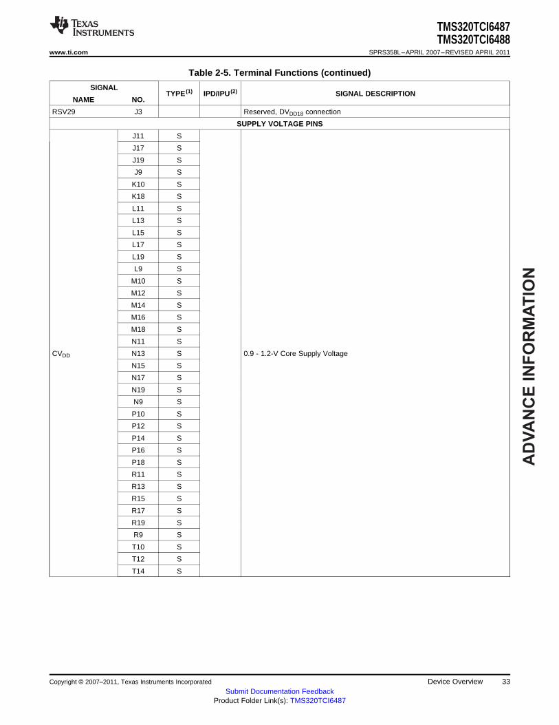
SUPPLY VOLTAGE PINS
J11 S
J17 S
J19 S
J9 S
K10 S
K18 S
L11 S
L13 S
L15 S
L17 S
L19 S
L9 S
M10 S
M12 S
M14 S
M16 S
M18 S
N11 S
CVDD N13 S 0.9 - 1.2-V Core Supply Voltage
N15 S
N17 S
N19 S
N9 S
P10 S
P12 S
P14 S
P16 S
P18 S
R11 S
R13 S
R15 S
R17 S
R19 S
R9 S
T10 S
T12 S
T14 S
Copyright © 2007–2011, Texas Instruments Incorporated Device Overview 33Submit Documentation Feedback
Product Folder Link(s): TMS320TCI6487

AD
VA
NC
E IN
FO
RM
AT
ION
TMS320TCI6487TMS320TCI6488SPRS358L–APRIL 2007–REVISED APRIL 2011 www.ti.com
Table 2-5. Terminal Functions (continued)
SIGNALTYPE (1) IPD/IPU (2) SIGNAL DESCRIPTION
NAME NO.
T16 S
T18 S
U11 S
U13 S
U15 S
U19 S
CVDD U9 S 0.9 - 1.2-V Core Supply Voltage
V10 S
V12 S
V14 S
W11 S
W13 S
W9 S
AC12 A
AC15 AAIF_V DDA11 1.1-V AIF Serdes Analog Supply
AC18 A
AC21 A
D12 A
D18 ASGR_V DDA11 1.1-V SRIO/SGMII Serdes Analog Supply
E11 A
E15 A
AVDD218 AG23 A1.8-V PLL Supply
AVDD118 AG9 A
AG26 S
U17 S
V16 S
AIF _V DDD11 V18 S 1.1-V AIF Serdes Digital Supply
W15 S
W17 S
W19 S
J13 S
J15 S
SGR_V DDD11 K12 S 1.1-V SRIO/SGMII Serdes Digital Supply
K14 S
K16 S
CVDDMON AG6 S 0.9 - 1.2-V CVDD Supply Monitor
AD19 SAIF_VDDR18 1.8-V AIF Serdes Regulator Supply
AD15 S
C12 SSGR_VDDR18 1.8-V SRIO/SGMII Serdes Regulator Supply
A18 S
34 Device Overview Copyright © 2007–2011, Texas Instruments Incorporated
Submit Documentation FeedbackProduct Folder Link(s): TMS320TCI6487
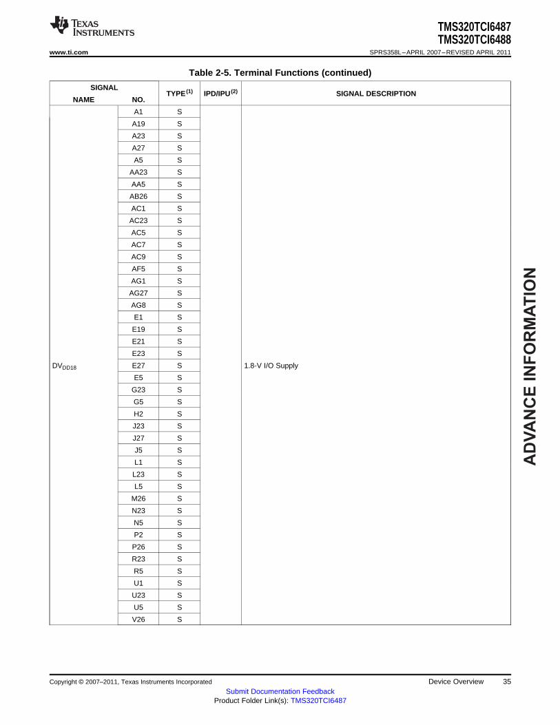
AD
VA
NC
E I
NF
OR
MA
TIO
N
TMS320TCI6487TMS320TCI6488
www.ti.com SPRS358L–APRIL 2007–REVISED APRIL 2011
Table 2-5. Terminal Functions (continued)
SIGNALTYPE (1) IPD/IPU (2) SIGNAL DESCRIPTION
NAME NO.
A1 S
A19 S
A23 S
A27 S
A5 S
AA23 S
AA5 S
AB26 S
AC1 S
AC23 S
AC5 S
AC7 S
AC9 S
AF5 S
AG1 S
AG27 S
AG8 S
E1 S
E19 S
E21 S
E23 S
DVDD18 E27 S 1.8-V I/O Supply
E5 S
G23 S
G5 S
H2 S
J23 S
J27 S
J5 S
L1 S
L23 S
L5 S
M26 S
N23 S
N5 S
P2 S
P26 S
R23 S
R5 S
U1 S
U23 S
U5 S
V26 S
Copyright © 2007–2011, Texas Instruments Incorporated Device Overview 35Submit Documentation Feedback
Product Folder Link(s): TMS320TCI6487

AD
VA
NC
E IN
FO
RM
AT
ION
TMS320TCI6487TMS320TCI6488SPRS358L–APRIL 2007–REVISED APRIL 2011 www.ti.com
Table 2-5. Terminal Functions (continued)
SIGNALTYPE (1) IPD/IPU (2) SIGNAL DESCRIPTION
NAME NO.
W23 S
W5 SDVDD18 1.8-V I/O Supply
Y2 S
Y24 S
DVDD18MON AG7 S 1.8-V DVDD18 Supply Monitor
AC11 S
AC14 S
AC17 S
AIF_VDDT11 AC20 S 1.1-V AIF Serdes Termination Supply
AF15 S
AF19 S
AG11 S
B13 S
B17 S
B8 SSGR_VDDT11 1.1-V SRIO/SGMII Serdes Termination Supply
E13 S
E17 S
E9 S
36 Device Overview Copyright © 2007–2011, Texas Instruments Incorporated
Submit Documentation FeedbackProduct Folder Link(s): TMS320TCI6487
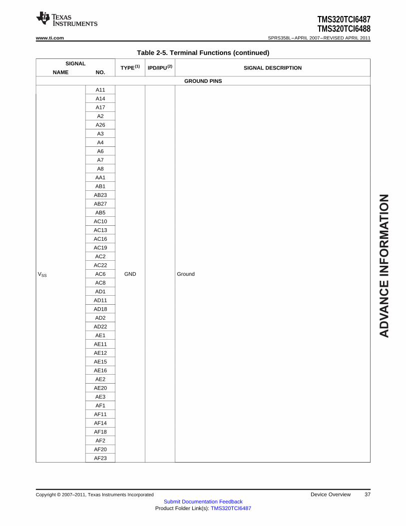
AD
VA
NC
E I
NF
OR
MA
TIO
N
TMS320TCI6487TMS320TCI6488
www.ti.com SPRS358L–APRIL 2007–REVISED APRIL 2011
Table 2-5. Terminal Functions (continued)
SIGNALTYPE (1) IPD/IPU (2) SIGNAL DESCRIPTION
NAME NO.
GROUND PINS
A11
A14
A17
A2
A26
A3
A4
A6
A7
A8
AA1
AB1
AB23
AB27
AB5
AC10
AC13
AC16
AC19
AC2
AC22
VSS AC6 GND Ground
AC8
AD1
AD11
AD18
AD2
AD22
AE1
AE11
AE12
AE15
AE16
AE2
AE20
AE3
AF1
AF11
AF14
AF18
AF2
AF20
AF23
Copyright © 2007–2011, Texas Instruments Incorporated Device Overview 37Submit Documentation Feedback
Product Folder Link(s): TMS320TCI6487
AD
VA
NC
E IN
FO
RM
AT
ION
TMS320TCI6487TMS320TCI6488SPRS358L–APRIL 2007–REVISED APRIL 2011 www.ti.com
Table 2-5. Terminal Functions (continued)
SIGNALTYPE (1) IPD/IPU (2) SIGNAL DESCRIPTION
NAME NO.
AF26
AF27
AF3
AF8
AG12
AG15
AG16
AG19
AG2
AG22
AG3
AG4
AG5
B1
B10
B11
B14
B15
B16
B2
B23
VSS B3 GND Ground
B4
B5
B6
B7
B9
C1
C15
C18
C2
C24
C3
C8
D1
D10
D11
D13
D14
D15
D16
D17
D2
38 Device Overview Copyright © 2007–2011, Texas Instruments Incorporated
Submit Documentation FeedbackProduct Folder Link(s): TMS320TCI6487
AD
VA
NC
E I
NF
OR
MA
TIO
N
TMS320TCI6487TMS320TCI6488
www.ti.com SPRS358L–APRIL 2007–REVISED APRIL 2011
Table 2-5. Terminal Functions (continued)
SIGNALTYPE (1) IPD/IPU (2) SIGNAL DESCRIPTION
NAME NO.
D23
D3
D8
E10
E12
E14
E16
E18
E2
E20
E22
E26
E8
F1
F23
F5
G1
G24
H1
H23
H5
VSS J10 GND Ground
J12
J14
J16
J18
J26
K11
K13
K15
K17
K19
K23
K5
K9
L10
L12
L14
L16
L18
L2
M11
M13
Copyright © 2007–2011, Texas Instruments Incorporated Device Overview 39Submit Documentation Feedback
Product Folder Link(s): TMS320TCI6487

AD
VA
NC
E IN
FO
RM
AT
ION
TMS320TCI6487TMS320TCI6488SPRS358L–APRIL 2007–REVISED APRIL 2011 www.ti.com
Table 2-5. Terminal Functions (continued)
SIGNALTYPE (1) IPD/IPU (2) SIGNAL DESCRIPTION
NAME NO.
M15
M17
M19
M23
M27
M5
M9
N10
N12
N14
N16
N18
P1
P11
P13
P15
P17
P19
P23
P27
P5
VSS P9 GND Ground
R10
R12
R14
R16
R18
R24
T11
T13
T15
T17
T19
T23
T27
T5
T9
U10
U12
U14
U16
U18
U2
40 Device Overview Copyright © 2007–2011, Texas Instruments Incorporated
Submit Documentation FeedbackProduct Folder Link(s): TMS320TCI6487
AD
VA
NC
E I
NF
OR
MA
TIO
N
TMS320TCI6487TMS320TCI6488
www.ti.com SPRS358L–APRIL 2007–REVISED APRIL 2011
Table 2-5. Terminal Functions (continued)
SIGNALTYPE (1) IPD/IPU (2) SIGNAL DESCRIPTION
NAME NO.
U24
V11
V13
V15
V17
V19
V23
V27
V5VSS GND Ground
V9
W10
W12
W14
W16
W18
Y1
Y23
Y5
Copyright © 2007–2011, Texas Instruments Incorporated Device Overview 41Submit Documentation Feedback
Product Folder Link(s): TMS320TCI6487
AD
VA
NC
E IN
FO
RM
AT
ION
TMS320TCI6487TMS320TCI6488SPRS358L–APRIL 2007–REVISED APRIL 2011 www.ti.com
2.8 Development and Device Support
2.8.1 Development Support
In case the customer would like to develop their own features and software on the TCI6487/8 device, TIoffers an extensive line of development tools for the TMS320C6000 DSP platform, including tools toevaluate the performance of the processors, generate code, develop algorithm implementations, and fullyintegrate and debug software and hardware modules. The tool's support documentation is electronicallyavailable within the Code Composer Studio™ Integrated Development Environment (IDE). The followingproducts support development of C6000 DSP-based applications:
Software Development Tools: Code Composer Studio Integrated Development Environment (IDE):including Editor C/C++/Assembly Code Generation, and Debug plus additional development toolsScalable, Real-Time Foundation Software (DSP/BIOS™), which provides the basic run-time targetsoftware needed to support any DSP application.
Hardware Development Tools: Extended Development System (XDS™) Emulator (supports C6000 DSPmultiprocessor system debug) Evaluation Module (EVM).
2.8.2 Device Nomenclature
To designate the stages in the product development cycle, TI assigns prefixes to the part numbers of allDSP devices and support tools. Each DSP commercial family member has one of three prefixes: TMX,TMP, or TMS (e.g., TMS320TCI6487ZUN). Texas Instruments recommends two of three possible prefixdesignators for its support tools: TMDX and TMDS. These prefixes represent evolutionary stages ofproduct development from engineering prototypes (TMX/TMDX) through fully qualified productiondevices/tools (TMS/TMDS).
Device development evolutionary flow:• TMX: Experimental device that is not necessarily representative of the final device's electrical
specifications.• TMP: Final silicon die that conforms to the device's electrical specifications but has not completed
quality and reliability verification.• TMS: Fully qualified production device.
Support tool development evolutionary flow:• TMDX: Development-support product that has not yet completed Texas Instruments internal
qualification testing.• TMDS: Fully qualified development-support product .
TMX and TMP devices and TMDX development-support tools are shipped with against the followingdisclaimer:
"Developmental product is intended for internal evaluation purposes."
TMS devices and TMDS development-support tools have been characterized fully, and the quality andreliability of the device have been demonstrated fully. TI's standard warranty applies.
Predictions show that prototype devices (TMX or TMP) have a greater failure rate than the standardproduction devices. Texas Instruments recommends that these devices not be used in any productionsystem because their expected end-use failure rate still is undefined. Only qualified production devices areto be used.
42 Device Overview Copyright © 2007–2011, Texas Instruments Incorporated
Submit Documentation FeedbackProduct Folder Link(s): TMS320TCI6487

AD
VA
NC
E I
NF
OR
MA
TIO
N
C64x+ DSP:TCI6487TCI6488
PREFIX
TMX 320 TCI6487 ZUN
TMX = Experimental deviceTMS = Qualified device
DEVICE FAMILY
320 = TMS320 DSP familyä
PACKAGE TYPE(A)
CUN = 561-pin plastic BGA (lead-free die bump and solder balls)GUN = 561-pin plastic BGA (leaded [Pb] solder balls)ZUN = 561-pin plastic BGA (lead-free solder balls and leaded [Pb] die bumps)
DEVICE
DEVICE SPEED RANGE
Blank = 1.0 GHz2 = 1.2 GHz
( )
TEMPERATURE RANGEBlank = 0 C to 100 C (default commercial temperature; 1.0-GHz device)
lank = 0°C to 95°C (default commercial temperature )
° °
; 1.0-GHz device; 1.2-GHz device
A = -40 C to 100 C (extended temperature )B
° °
A = -40 C to 95 C (extended temperature )° ° ; 1.2-GHz device
2
TMS320TCI6487TMS320TCI6488
www.ti.com SPRS358L–APRIL 2007–REVISED APRIL 2011
TI device nomenclature also includes a suffix with the device family name. This suffix indicates thepackage type (for example, ZUN), the temperature range (for example, Blank is the default commercialtemperature range), and the device speed range in megahertz (for example, 2 is 1200 [1.2 GHz]).Figure 2-11 provides a legend for reading the complete device name for any TMS320C64x+ DSPgeneration member. For device part numbers and further ordering information for TMS320TCI6487/8 inthe CUN, GUN, or ZUN package type, see the TI website (www.ti.com) or contact your TI salesrepresentative.
A. BGA = Ball Grid Array
Figure 2-11. TMS320C64x+™ DSP Device Nomenclature (including TMS320TCI6487/8 DSP)
2.9 Documentation Support
The following documents describe the TMS320TCI6487/8 communications infrastructure digital signalprocessor. Copies of these documents are available on the Internet at www.ti.com. Tip: Enter the literaturenumber in the search box provided at www.ti.com.
SPRU732 TMS320C64x/C64x+ DSP CPU and Instruction Set Reference Guide. Describes the CPUarchitecture, pipeline, instruction set, and interrupts for the TMS320C64x and TMS320C64x+digital signal processors (DSPs) of the TMS320C6000 DSP family. The C64x/C64x+ DSPgeneration comprises fixed-point devices in the C6000 DSP platform. The C64x+ DSP is anenhancement of the C64x DSP with added functionality and an expanded instruction set.
SPRU871 TMS320C64x+ DSP Megamodule Reference Guide. Describes the TMS320C64x+ digitalsignal processor (DSP) megamodule. Included is a discussion on the internal direct memoryaccess (IDMA) controller, the interrupt controller, the power-down controller, memoryprotection, bandwidth management, and the memory and cache.
SPRAA84 TMS320C64x to TMS320C64x+ CPU Migration Guide. Describes migrating from the TexasInstruments TMS320C64x digital signal processor (DSP) to the TMS320C64x+ DSP. Theobjective of this document is to indicate differences between the two cores. Functionality inthe devices that is identical is not included.
SPRU889 High-Speed DSP Systems Design Reference Guide. Provides recommendations formeeting the many challenges of high-speed DSP system design. These recommendationsinclude information about DSP audio, video, and communications systems for the C5000 andC6000 DSP platforms.
SPRU725 TMS320C6472/TMS320TCI648x DSP General-Purpose Input/Output (GPIO) User’sGuide. This document describes the general-purpose input/output (GPIO) peripheral in thedigital signal processors (DSPs) of the TMS320C6472/TMS320TCI648x DSP family.
SPRU803 TMS320TCI648x DSP Multichannel Buffered Serial Port (McBSP) Reference Guide. Thisdocument describes the operation of the multichannel buffered serial port (McBSP) in thedigital signal processors (DSPs) of the TMS320TCI648x devices.
SPRU818 TMS320C6472/TMS320TCI648x DSP 64-Bit Timer User’s Guide. This document provides
Copyright © 2007–2011, Texas Instruments Incorporated Device Overview 43Submit Documentation Feedback
Product Folder Link(s): TMS320TCI6487
AD
VA
NC
E IN
FO
RM
AT
ION
TMS320TCI6487TMS320TCI6488SPRS358L–APRIL 2007–REVISED APRIL 2011 www.ti.com
an overview of the 64-bit timer in the TMS320C6472/TMS320TCI648x DSP.
SPRU894 TMS320C6472/TMS320TCI648x DSP DDR2 Memory Controller User's Guide. Thisdocument describes the DDR2 memory controller in the TMS320C6472/TMS320TCI648xdigital signal processors (DSPs).
SPRUE09 TMS320TCI648x DSP Viterbi-Decoder Coprocessor 2 (VCP2) Reference Guide. Thisdocument describes the operation and programming of the VCP2 in the TMS320TCI648xdigital signal processors (DSPs).
SPRUE10 TMS320TCI648x DSP Turbo-Decoder Coprocessor 2 (TCP2) Reference Guide. Thisdocument describes the operation and programming of the TCP2 in the TMS320TCI648xdigital signal processors (DSPs).
SPRUE11 TMS320C6472/TMS320TCI648x DSP Inter-Integrated Circuit (I2C) Module User's Guide.This document describes the inter-integrated circuit (I2C) module in theTMS320C6472/TMS320TCI648x digital signal processors (DSPs).
SPRUE13 TMS320C6472/TMS320TCI648x Serial RapidIO (SRIO) User's Guide. This documentdescribes the Serial RapidIO (SRIO) on the TMS320C6472/TMS320TCI648x devices.
SPRUEE9 TMS320TCI6487/8 DSP Enhanced DMA (EDMA3) Controller User's Guide. Thisdocument describes the Enhanced DMA (EDMA3) Controller on the TMS320TCI6487/8digital signal processors (DSPs).
SPRUEF0 TMS320TCI6487/8 DSP Ethernet Media Access Controller (EMAC)/ Management DataInput/Output (MDIO) User's Guide. This document provides a functional description of theEthernet Media Access Controller (EMAC) and Physical layer (PHY) device ManagementData Input/Output (MDIO) module integrated with the TMS320TCI6487/8 digital signalprocessors (DSPs).
SPRUEF1 TMS320TCI6487/8 DSP Software-Programmable Phase-Locked Loop (PLL) ControllerUser's Guide. This document describes the operation of the software-programmablephase-locked loop (PLL) controller in the TMS320TCI6487/8 digital signal processors(DSPs).
SPRUEF3 TMS320TCI6487/8 Power/Sleep Controller (PSC) User's Guide. This document describesthe Power/Sleep Controller (PSC) for the TMS320TCI6487/8 digital signal processors(DSPs).
SPRUEF4 TMS320TCI6487/8 Antenna Interface User's Guide. This document describes the AntennaInterface module on the TMS320TCI6487/8 digital signal processors (DSPs).
SPRUEF5 TMS320TCI6487/8 Frame Synchronization User's Guide. This document describes thereference guide for Frame Synchronization module on the TMS320TCI6487/8 digital signalprocessors (DSPs).
SPRUEF6 TMS320TCI6487/8 Semaphore User's Guide. This document describes the usage of thesemaphore and some of the CSL calls used to configure/use the Semaphore module on theTMS320TCI6487/8 digital signal processors (DSPs).
SPRUEJ0 TMS320TCI6488 Receive Accelerator (RAC) User's Guide. This manual describes thereceive accelerator co-processor (RAC) on the TMS320TCI6488 digital signal processor(DSP).
SPRUG70 TMS320TCI6487/8 DSP Chip Interrupt Controller (CIC) User's Guide. This documentdescribes the system event routing using the chip interrupt controller (CIC) for theTMS320TCI6487/8 digital signal processors (DSPs).
SPRAAG5 TMS320TCI6488 Hardware Design Guide. This document describes hardware systemdesign considerations for the TMS320TCI6488.
SPRAAG6 TMS320TCI6484/6487/6488 DDR2 Implementation Guidelines. This document provides
44 Device Overview Copyright © 2007–2011, Texas Instruments Incorporated
Submit Documentation FeedbackProduct Folder Link(s): TMS320TCI6487

AD
VA
NC
E I
NF
OR
MA
TIO
N
TMS320TCI6487TMS320TCI6488
www.ti.com SPRS358L–APRIL 2007–REVISED APRIL 2011
implementation instructions for the DDR2 interface contained on theTMS320TCI6484/6487/6488 DSPs.
SPRAAG7 TMS320TCI6488 SERDES Implementation Guidelines. This document containsimplementation instructions for the three serializer/deserializer (SERDES) based interfaceson the TMS320TCI6488 DSP device. These include the Serial RapidIO® (SRIO), antenna,and serial gigabit media independent interface (SGMII) interfaces.
SPRAAM4 TMS320TCI6488 Receive Accelerator (RAC) Internal Precisions. This document providesprocessing decisions for the RAC internal sub-modules contained in the TCI6488 DSPdevice.
SPRAAN6 TMS320TCI6487/8 Module Throughput. This document provides information on theTMS320TCI6487/8 module throughput.
SPRAAN7 TMS320TCI6487/8 Common Bus Architecture (CBA) Throughput. This documentpresents common bus architecture protocols and components as main factors for genericthroughput analysis. It provides necessary details on the internal bus structure which enablesyou to estimate system-on-chip (SoC) performance for a given application.
SPRAAS3 TMS320TCI6488 Power Consumption Summary. This document discusses the powerconsumption of the Texas Instruments TMS320TCI6488 digital signal processor (DSP).
SPRAB27 TMS320TCI6487/8 Multicore Programming Guide. This document presents aprogramming methodology for converting applications to run on multicore devices. It alsodescribes the features of Texas Instruments DSPs that enable efficient implementation,execution, synchronization, and analysis of multicore applications.
The following additional application reports are available on request from the local support team:• TMS320TCI6487/8 Power-On Self Test application report (literature number SPRAAR1)• TMS320TCI6487/8 Thermal Reference Guide• TMS320TCI6487/8 Preliminary (v1.8) Capacitor Selection application report
2.10 Community Resources
The following links connect to TI community resources. Linked contents are provided "AS IS" by therespective contributors. They do not constitute TI specifications and do not necessarily reflect TI's views;see TI's Terms of Use.
TI E2E Community TI's Engineer-to-Engineer (E2E) Community. Created to foster collaborationamong engineers. At e2e.ti.com, you can ask questions, share knowledge, explore ideas andhelp solve problems with fellow engineers.
TI Embedded Processors Wiki Texas Instruments Embedded Processors Wiki. Established to helpdevelopers get started with Embedded Processors from Texas Instruments and to fosterinnovation and growth of general knowledge about the hardware and software surroundingthese devices.
Copyright © 2007–2011, Texas Instruments Incorporated Device Overview 45Submit Documentation Feedback
Product Folder Link(s): TMS320TCI6487
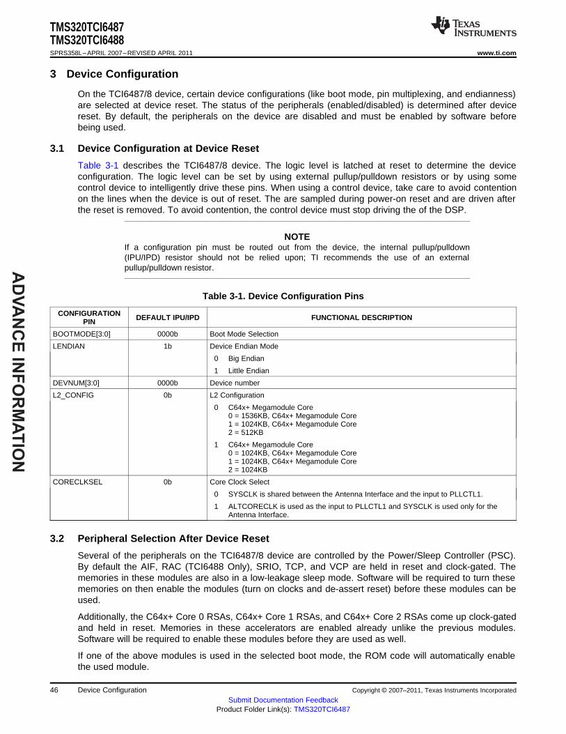
AD
VA
NC
E IN
FO
RM
AT
ION
TMS320TCI6487TMS320TCI6488SPRS358L–APRIL 2007–REVISED APRIL 2011 www.ti.com
3 Device Configuration
On the TCI6487/8 device, certain device configurations (like boot mode, pin multiplexing, and endianness)are selected at device reset. The status of the peripherals (enabled/disabled) is determined after devicereset. By default, the peripherals on the device are disabled and must be enabled by software beforebeing used.
3.1 Device Configuration at Device Reset
Table 3-1 describes the TCI6487/8 device. The logic level is latched at reset to determine the deviceconfiguration. The logic level can be set by using external pullup/pulldown resistors or by using somecontrol device to intelligently drive these pins. When using a control device, take care to avoid contentionon the lines when the device is out of reset. The are sampled during power-on reset and are driven afterthe reset is removed. To avoid contention, the control device must stop driving the of the DSP.
NOTEIf a configuration pin must be routed out from the device, the internal pullup/pulldown(IPU/IPD) resistor should not be relied upon; TI recommends the use of an externalpullup/pulldown resistor.
Table 3-1. Device Configuration Pins
CONFIGURATION DEFAULT IPU/IPD FUNCTIONAL DESCRIPTIONPIN
BOOTMODE[3:0] 0000b Boot Mode Selection
LENDIAN 1b Device Endian Mode
0 Big Endian
1 Little Endian
DEVNUM[3:0] 0000b Device number
L2_CONFIG 0b L2 Configuration
0 C64x+ Megamodule Core0 = 1536KB, C64x+ Megamodule Core1 = 1024KB, C64x+ Megamodule Core2 = 512KB
1 C64x+ Megamodule Core0 = 1024KB, C64x+ Megamodule Core1 = 1024KB, C64x+ Megamodule Core2 = 1024KB
CORECLKSEL 0b Core Clock Select
0 SYSCLK is shared between the Antenna Interface and the input to PLLCTL1.
1 ALTCORECLK is used as the input to PLLCTL1 and SYSCLK is used only for theAntenna Interface.
3.2 Peripheral Selection After Device Reset
Several of the peripherals on the TCI6487/8 device are controlled by the Power/Sleep Controller (PSC).By default the AIF, RAC (TCI6488 Only), SRIO, TCP, and VCP are held in reset and clock-gated. Thememories in these modules are also in a low-leakage sleep mode. Software will be required to turn thesememories on then enable the modules (turn on clocks and de-assert reset) before these modules can beused.
Additionally, the C64x+ Core 0 RSAs, C64x+ Core 1 RSAs, and C64x+ Core 2 RSAs come up clock-gatedand held in reset. Memories in these accelerators are enabled already unlike the previous modules.Software will be required to enable these modules before they are used as well.
If one of the above modules is used in the selected boot mode, the ROM code will automatically enablethe used module.
46 Device Configuration Copyright © 2007–2011, Texas Instruments Incorporated
Submit Documentation FeedbackProduct Folder Link(s): TMS320TCI6487
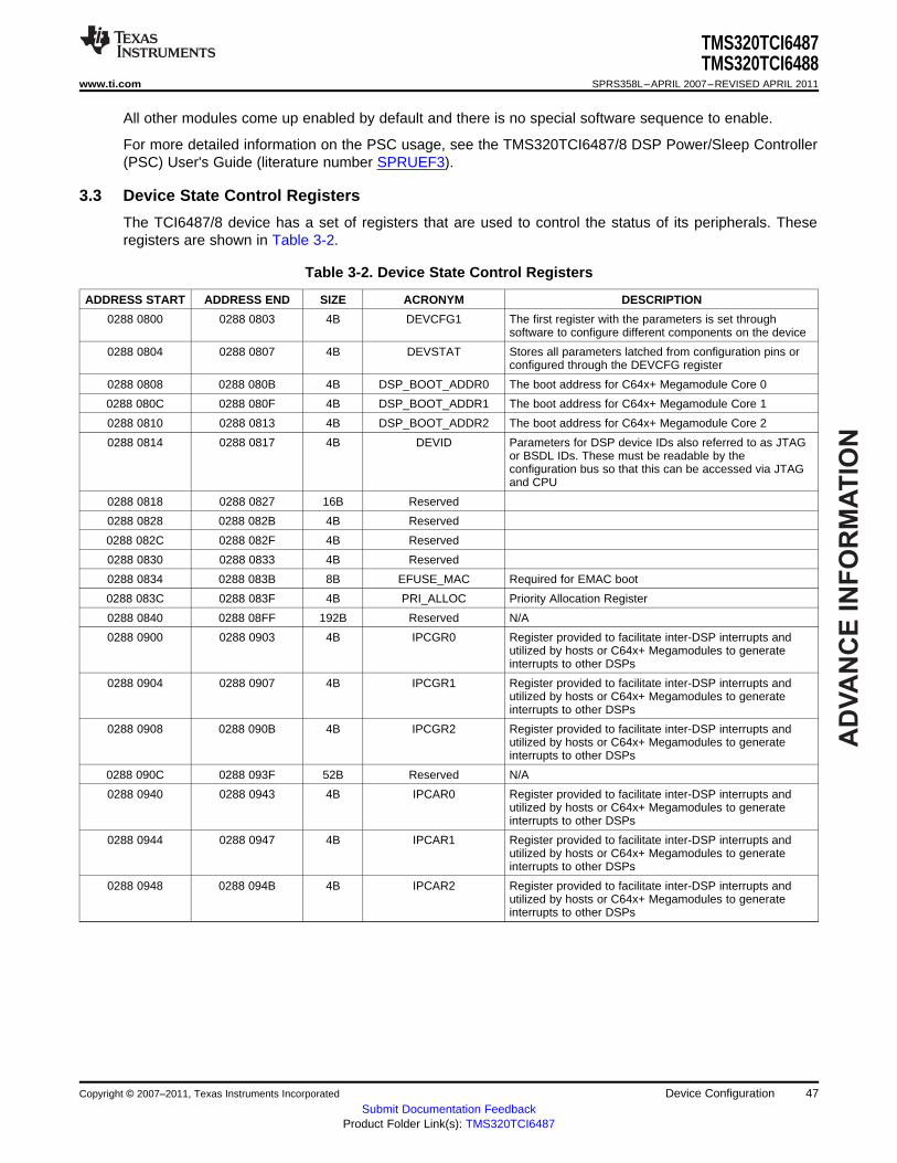
AD
VA
NC
E I
NF
OR
MA
TIO
N
TMS320TCI6487TMS320TCI6488
www.ti.com SPRS358L–APRIL 2007–REVISED APRIL 2011
All other modules come up enabled by default and there is no special software sequence to enable.
For more detailed information on the PSC usage, see the TMS320TCI6487/8 DSP Power/Sleep Controller(PSC) User's Guide (literature number SPRUEF3).
3.3 Device State Control Registers
The TCI6487/8 device has a set of registers that are used to control the status of its peripherals. Theseregisters are shown in Table 3-2.
Table 3-2. Device State Control Registers
ADDRESS START ADDRESS END SIZE ACRONYM DESCRIPTION
0288 0800 0288 0803 4B DEVCFG1 The first register with the parameters is set throughsoftware to configure different components on the device
0288 0804 0288 0807 4B DEVSTAT Stores all parameters latched from configuration pins orconfigured through the DEVCFG register
0288 0808 0288 080B 4B DSP_BOOT_ADDR0 The boot address for C64x+ Megamodule Core 0
0288 080C 0288 080F 4B DSP_BOOT_ADDR1 The boot address for C64x+ Megamodule Core 1
0288 0810 0288 0813 4B DSP_BOOT_ADDR2 The boot address for C64x+ Megamodule Core 2
0288 0814 0288 0817 4B DEVID Parameters for DSP device IDs also referred to as JTAGor BSDL IDs. These must be readable by theconfiguration bus so that this can be accessed via JTAGand CPU
0288 0818 0288 0827 16B Reserved
0288 0828 0288 082B 4B Reserved
0288 082C 0288 082F 4B Reserved
0288 0830 0288 0833 4B Reserved
0288 0834 0288 083B 8B EFUSE_MAC Required for EMAC boot
0288 083C 0288 083F 4B PRI_ALLOC Priority Allocation Register
0288 0840 0288 08FF 192B Reserved N/A
0288 0900 0288 0903 4B IPCGR0 Register provided to facilitate inter-DSP interrupts andutilized by hosts or C64x+ Megamodules to generateinterrupts to other DSPs
0288 0904 0288 0907 4B IPCGR1 Register provided to facilitate inter-DSP interrupts andutilized by hosts or C64x+ Megamodules to generateinterrupts to other DSPs
0288 0908 0288 090B 4B IPCGR2 Register provided to facilitate inter-DSP interrupts andutilized by hosts or C64x+ Megamodules to generateinterrupts to other DSPs
0288 090C 0288 093F 52B Reserved N/A
0288 0940 0288 0943 4B IPCAR0 Register provided to facilitate inter-DSP interrupts andutilized by hosts or C64x+ Megamodules to generateinterrupts to other DSPs
0288 0944 0288 0947 4B IPCAR1 Register provided to facilitate inter-DSP interrupts andutilized by hosts or C64x+ Megamodules to generateinterrupts to other DSPs
0288 0948 0288 094B 4B IPCAR2 Register provided to facilitate inter-DSP interrupts andutilized by hosts or C64x+ Megamodules to generateinterrupts to other DSPs
Copyright © 2007–2011, Texas Instruments Incorporated Device Configuration 47Submit Documentation Feedback
Product Folder Link(s): TMS320TCI6487

AD
VA
NC
E IN
FO
RM
AT
ION
TMS320TCI6487TMS320TCI6488SPRS358L–APRIL 2007–REVISED APRIL 2011 www.ti.com
3.4 Device Status Register Descriptions
The device status register depicts the device configuration selected upon device reset. Once set, thesebits remain set until a device reset.
Figure 3-1 shows the device configuration register 1 and Table 3-3 describes the parameters that are setthrough software to configure different components on the device. The configuration is done through thedevice configuration DEVCFG register, which is one-time writeable through software. The register is reseton all hard resets and is locked after the first write.
31 3 2 1 0
Reserved CLKS1 CLKS0 SYSCLKOUTEN
R-00000000000000000000000000000 R/W-0 R/W-0 R/W-1
LEGEND: R/W = Read/Write; R = Read only; -n = value after reset
Figure 3-1. Device Configuration Register (DEVCFG)
Table 3-3. Device Configuration Register (DEVCFG) Field Descriptions
Bit Field Value Description
31:3 Reserved Reserved
2 CLKS1 McBSP1 CLKS Select
0 CLKS1 device pin
1 chip_clks from Main.PLL
1 CLKS0 McBSP0 CLKS Select
0 CLKS0 device pin
1 chip_clks from Main.PLL
0 SYSCLKOUTEN SYSCLKOUT Enable
0 No Clock Output
1 Clock output Enabled
48 Device Configuration Copyright © 2007–2011, Texas Instruments Incorporated
Submit Documentation FeedbackProduct Folder Link(s): TMS320TCI6487
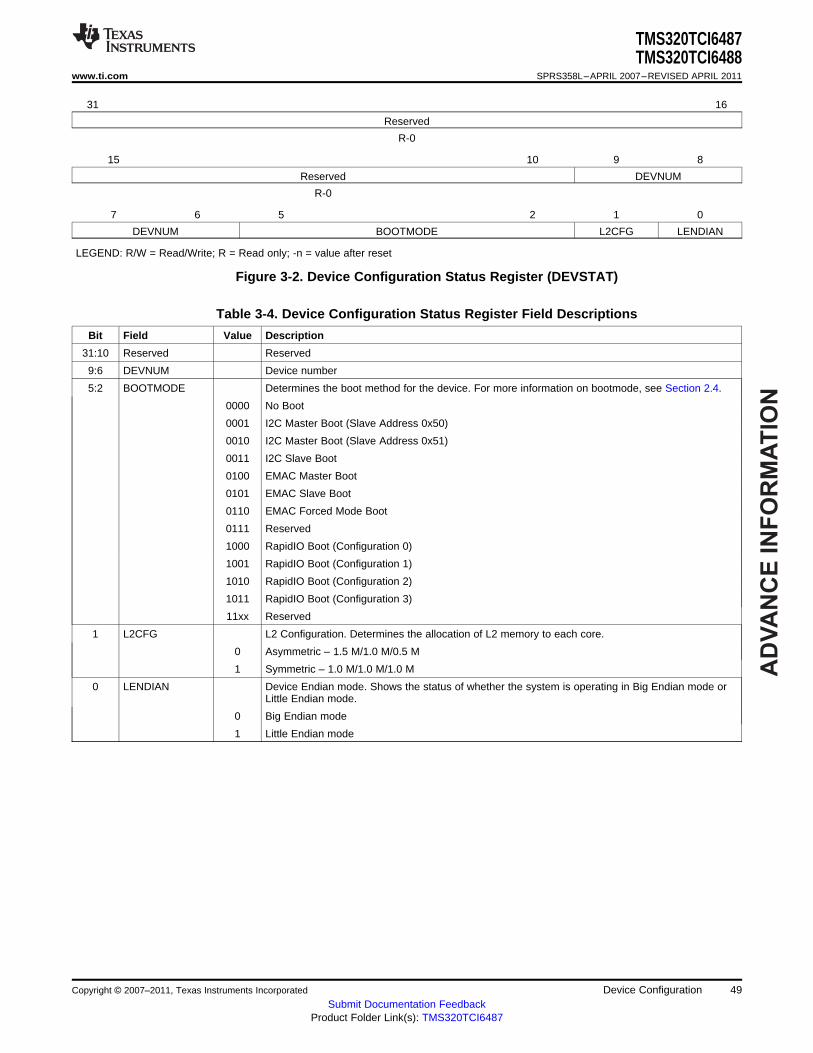
AD
VA
NC
E I
NF
OR
MA
TIO
N
TMS320TCI6487TMS320TCI6488
www.ti.com SPRS358L–APRIL 2007–REVISED APRIL 2011
31 16
Reserved
R-0
15 10 9 8
Reserved DEVNUM
R-0
7 6 5 2 1 0
DEVNUM BOOTMODE L2CFG LENDIAN
LEGEND: R/W = Read/Write; R = Read only; -n = value after reset
Figure 3-2. Device Configuration Status Register (DEVSTAT)
Table 3-4. Device Configuration Status Register Field Descriptions
Bit Field Value Description
31:10 Reserved Reserved
9:6 DEVNUM Device number
5:2 BOOTMODE Determines the boot method for the device. For more information on bootmode, see Section 2.4.
0000 No Boot
0001 I2C Master Boot (Slave Address 0x50)
0010 I2C Master Boot (Slave Address 0x51)
0011 I2C Slave Boot
0100 EMAC Master Boot
0101 EMAC Slave Boot
0110 EMAC Forced Mode Boot
0111 Reserved
1000 RapidIO Boot (Configuration 0)
1001 RapidIO Boot (Configuration 1)
1010 RapidIO Boot (Configuration 2)
1011 RapidIO Boot (Configuration 3)
11xx Reserved
1 L2CFG L2 Configuration. Determines the allocation of L2 memory to each core.
0 Asymmetric – 1.5 M/1.0 M/0.5 M
1 Symmetric – 1.0 M/1.0 M/1.0 M
0 LENDIAN Device Endian mode. Shows the status of whether the system is operating in Big Endian mode orLittle Endian mode.
0 Big Endian mode
1 Little Endian mode
Copyright © 2007–2011, Texas Instruments Incorporated Device Configuration 49Submit Documentation Feedback
Product Folder Link(s): TMS320TCI6487
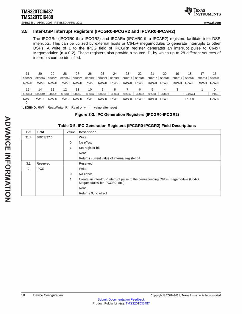
AD
VA
NC
E IN
FO
RM
AT
ION
TMS320TCI6487TMS320TCI6488SPRS358L–APRIL 2007–REVISED APRIL 2011 www.ti.com
3.5 Inter-DSP Interrupt Registers (IPCGR0-IPCGR2 and IPCAR0-IPCAR2)
The IPCGRn (IPCGR0 thru IPCGR2) and IPCARn (IPCAR0 thru IPCAR2) registers facilitate inter-DSPinterrupts. This can be utilized by external hosts or C64x+ megamodules to generate interrupts to otherDSPs. A write of 1 to the IPCG field of IPCGRn register generates an interrupt pulse to C64x+Megamodulen (n = 0-2). These registers also provide a source ID, by which up to 28 different sources ofinterrupts can be identified.
31 30 29 28 27 26 25 24 23 22 21 20 19 18 17 16SRCS27 SRCS26 SRCS25 SRCS24 SRCS23 SRCS22 SRCS21 SRCS20 SRCS19 SRCS18 SRCS17 SRCS16 SRCS15 SRCS14 SRCS13 SRCS12
R/W-0 R/W-0 R/W-0 R/W-0 R/W-0 R/W-0 R/W-0 R/W-0 R/W-0 R/W-0 R/W-0 R/W-0 R/W-0 R/W-0 R/W-0 R/W-0
15 14 13 12 11 10 9 8 7 6 5 4 3 1 0SRCS11 SRCS10 SRCS9 SRCS8 SRCS7 SRCS6 SRCS5 SRCS4 SRCS3 SRCS2 SRCS1 SRCS0 Reserved IPCG
R/W- R/W-0 R/W-0 R/W-0 R/W-0 R/W-0 R/W-0 R/W-0 R/W-0 R/W-0 R/W-0 R/W-0 R-000 R/W-00
LEGEND: R/W = Read/Write; R = Read only; -n = value after reset
Figure 3-3. IPC Generation Registers (IPCGR0-IPCGR2)
Table 3-5. IPC Generation Registers (IPCGR0-IPCGR2) Field Descriptions
Bit Field Value Description
31:4 SRCS[27:0] Write:
0 No effect
1 Set register bit
Read:
Returns current value of internal register bit
3:1 Reserved Reserved
0 IPCG Write:
0 No effect
1 Create an inter-DSP interrupt pulse to the corresponding C64x+ megamodule (C64x+Megamodule0 for IPCGR0, etc.)
Read:
Returns 0, no effect
50 Device Configuration Copyright © 2007–2011, Texas Instruments Incorporated
Submit Documentation FeedbackProduct Folder Link(s): TMS320TCI6487

AD
VA
NC
E I
NF
OR
MA
TIO
N
TMS320TCI6487TMS320TCI6488
www.ti.com SPRS358L–APRIL 2007–REVISED APRIL 2011
31 30 29 28 27 26 25 24 23 22 21 20 19 18 17 16SRCC27 SRCC26 SRCC25 SRCC24 SRCC23 SRCC22 SRCC21 SRCC20 SRCC19 SRCC18 SRCC17 SRCC16 SRCC15 SRCC14 SRCC13 SRCC12
R/W-0 R/W-0 R/W-0 R/W-0 R/W-0 R/W-0 R/W-0 R/W-0 R/W-0 R/W-0 R/W-0 R/W-0 R/W-0 R/W-0 R/W-0 R/W-0
15 14 13 12 11 10 9 8 7 6 5 4 3 0SRCC11 SRCC10 SRCC9 SRCC8 SRCC7 SRCC6 SRCC5 SRCC4 SRCC3 SRCC2 SRCC1 SRCC0 Reserved
R/W- R/W-0 R/W-0 R/W-0 R/W-0 R/W-0 R/W-0 R/W-0 R/W-0 R/W-0 R/W-0 R/W-0 R-00000
LEGEND: R/W = Read/Write; R = Read only; -n = value after reset
Figure 3-4. IPC Acknowledgment Registers (IPCAR0-IPCAR2)
Table 3-6. IPC Acknowledgment Registers (IPCAR0-IPCAR2) Field Descriptions
Bit Field Value Description
31:4 SRCC[27:0] Write:
0 No effect
1 Clear register bit
Read:
Returns current value of internal register bit
3:0 Reserved Reserved
3.6 JTAG ID (JTAGID) Register Description
The JTAG ID register is a read-only register that identifies to the customer the JTAG/Device ID. For theTCI6487/8 device, the JTAG ID register resides at address location 0x0288 0814. For the actual registerbit names and their associated bit field descriptions, see Figure 3-5 and Table 3-7.
31 28 27 12 11 1 0
VARIANT PART NUMBER MANUFACTURER LSB(4-bit) (16-bit) (11-bit)
R-n R-0000 0000 1001 0010b R-000 0001 0111b R-1
LEGEND: R = Read only; -n = value after reset
Figure 3-5. JTAG ID (JTAGID) Register
Table 3-7. JTAG ID (JTAGID) Register Field Descriptions
Bit Field Value Description
31:28 VARIANT Variant (4-Bit) value. The value of this field depends on the silicon revision being used.
Note: the VARIANT filed may be invalid if no CLKIN1 signal is applied.
27:12 PART NUMBER Part Number (16-Bit) value. TCI6487/8 value: 0000 0000 1001 0010b.
11:1 MANUFACTURER Manufacturer (11-Bit) value. TCI6487/8 value: 000 0001 0111b.
0 LSB LSB value. This bit is read as 1 for TCI6487/8.
3.7 Debugging Considerations
It is recommended that external connections be provided to device configuration pins. Although internalpullup/pulldown resistors exist on these pins, providing external connectivity adds convenience to the userin debugging and flexibility in switching operating modes.
For the internal pullup/pulldown resistors for all device pins, see Table 2-5.
Copyright © 2007–2011, Texas Instruments Incorporated Device Configuration 51Submit Documentation Feedback
Product Folder Link(s): TMS320TCI6487
AD
VA
NC
E IN
FO
RM
AT
ION
TMS320TCI6487TMS320TCI6488SPRS358L–APRIL 2007–REVISED APRIL 2011 www.ti.com
4 System Interconnect
On the TCI6487/8 device, the C64x+ Megamodule, the EDMA3 transfer controllers, and the systemperipherals are interconnected through two switch fabrics. The switch fabrics allow for low-latency,concurrent data transfers between master peripherals and slave peripherals. Through a switch fabric theCPU can send data to the Viterbi co-processor (VCP2) without affecting a data transfer through the RAC(TCI6488 only) and the DDR2 memory controller. The switch fabrics also allow for seamless arbitrationbetween the system masters when accessing system slaves.
4.1 Internal Buses, Switch Fabrics, and Bridges/Gaskets
Two types of buses exist in the TCI6487/8 device: data buses and configuration buses. Some TCI6487/8peripherals have both a data bus and a configuration bus interface, while others only have one type ofinterface. Furthermore, the bus interface width and speed varies from peripheral to peripheral.
Configuration buses are mainly used to access the register space of a peripheral and the data buses areused mainly for data transfers. However, in some cases, the configuration bus is also used to transferdata. For example, data is transferred to the VCP2 and TCP2 via their configuration bus interface.Similarly, the data bus can also be used to access the register space of a peripheral. For example, theDDR2 memory controller registers are accessed through their data bus interface.
The C64x+ megamodule, the EDMA3 transfer controllers, and the various system peripherals can beclassified into two categories: masters and slaves. Masters are capable of initiating read and writetransfers in the system and do not rely on the EDMA3 for their data transfers. Slaves on the other handrely on the EDMA3 to perform transfers to and from them. Examples of masters include the EDMA3transfer controllers, SRIO, and EMAC. Examples of slaves include the McBSP and I2C.
The TCI6487/8 device contains two switch fabrics through which masters and slaves communicate. Thedata switch fabric, known as the data switched central resource (SCR), is a high-throughput interconnectmainly used to move data across the system (for more information, see Section 4.3). The SCR adds nolatency and allows seamless arbitration (i.e., no dead cycles inserted by the fabric) between the mastersand slaves. The data SCR connects masters to slaves via 128-bit data buses (SCR B) and 64-bit databuses (SCR A) running at a CPU/3 frequency (CPU/3 is generated from PLL1 controller). Peripherals thathave a 128-bit data bus interface running at this speed can connect directly to the data SCR; otherperipherals require a bridge.
The configuration switch fabric, also known as the configuration switch central resource (SCR) is mainlyused by the C64x+ Megamodule to access peripheral registers (for more information, see Section 4.4).The configuration SCR connects C64x+ Megamodule to slaves via 32-bit configuration buses running at aCPU/3 frequency (CPU/3 is generated from PLL1 controller). As with the data SCR, some peripheralsrequire the use of a bridge to interface to the configuration SCR. Note that the data SCR also connects tothe configuration SCR.
Bridges and gaskets are required to perform a variety of functions. For the purpose of this document,bridges and gaskets can be considered as identical. Within the switch fabric infrastructure, gaskets aresimpler than bridges in that they only modify control signals to convert protocols. Bridges perform a varietyof functions:• Conversion between configuration bus and data bus.• Width conversion between peripheral bus width and SCR bus width.• Frequency conversion between peripheral bus frequency and SCR bus frequency.
For more information on the common bus architecture and its throughput in the TCI6487/8 device, see theTMS320TCI6487/8 Common Bus Architecture Throughput application report (literature number SPRAAN7)and the TMS320TCI6487/8 Module Throughput application report (literature number SPRAAN6).
52 System Interconnect Copyright © 2007–2011, Texas Instruments Incorporated
Submit Documentation FeedbackProduct Folder Link(s): TMS320TCI6487
AD
VA
NC
E I
NF
OR
MA
TIO
N
TMS320TCI6487TMS320TCI6488
www.ti.com SPRS358L–APRIL 2007–REVISED APRIL 2011
4.2 Data Switch Fabric Connections
Figure 4-1 shows the DMA switch fabric, including the EDMA3, connection between slaves and mastersthrough the data switched central resource (SCR). Masters are shown on the right and slaves on the left.The number of master ports for the EDMA is 2x the number of TPTCs implemented because each TPTChas a read port and a write port.
Copyright © 2007–2011, Texas Instruments Incorporated System Interconnect 53Submit Documentation Feedback
Product Folder Link(s): TMS320TCI6487

AD
VA
NC
E IN
FO
RM
AT
ION
EMAC
M
M
M
M S
S
S
S
M
M
M
S
S
S
S
S
x6
SM
S
x6
MS
MS
M
M
S
M
64
64
32 64
128
64
64
64
128
128
128
64
64 32
32
64M
32
S
S
M
M
M
M
128
128
64
64
32
M
S
S
128
S64
32
S
M
128
M S6464
64S
128
M
M S
S
x6 x6
128
128
64 64
64 64
M
32
S
S
M32 6432
SM128 128
S
M64 64
64
64
64
Chip events
ChannelController
(CC)64 channels
TransferController
(TC)3 channels
Bridge6
Bridge7
Bridge25
Bridge16
Bridge17
Bridge5
RapidIO
RapidIOCPPI
RAC Back-
End 1(A)
C64x+Megamodule
Core 1
C64x+Megamodule
Core 2
C64x+Megamodule
Core 3
Bridge4
Bridge3
Bridge2
SCR B64-bit
VBUSM
TransferController
(TC)3 channels
RAC Back-
End 0(A)
Bridge1
SCR A128-bitVBUSM
Bridge22
Bridge23
Bridge24
AIF Read
AIF Write
C64x+Megamodule
Core 1
C64x+Megamodule
Core 2
C64x+Megamodule
Core 3
Bridge18
Bridge9
SC
RC
32-b
itV
BU
SP
Bridge27
ROM
DDR2EMIF
RAC Front-
End(A)
MCBSPs(2)
Bridge28
Bridge12
Bridge11
Bridge29
Bridge10
SCRD(CFG)
VCP
TCP
TMS320TCI6487TMS320TCI6488SPRS358L–APRIL 2007–REVISED APRIL 2011 www.ti.com
A. TCI6488 only.
Figure 4-1. Switched Central Resource Block Diagram
54 System Interconnect Copyright © 2007–2011, Texas Instruments Incorporated
Submit Documentation FeedbackProduct Folder Link(s): TMS320TCI6487
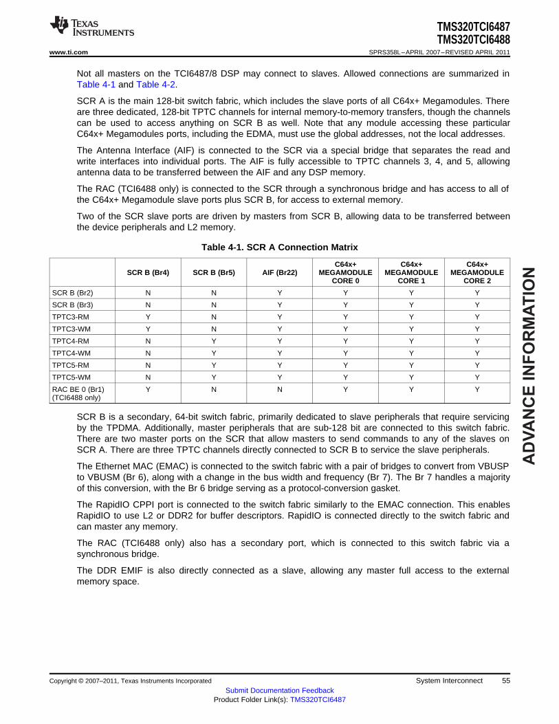
AD
VA
NC
E I
NF
OR
MA
TIO
N
TMS320TCI6487TMS320TCI6488
www.ti.com SPRS358L–APRIL 2007–REVISED APRIL 2011
Not all masters on the TCI6487/8 DSP may connect to slaves. Allowed connections are summarized inTable 4-1 and Table 4-2.
SCR A is the main 128-bit switch fabric, which includes the slave ports of all C64x+ Megamodules. Thereare three dedicated, 128-bit TPTC channels for internal memory-to-memory transfers, though the channelscan be used to access anything on SCR B as well. Note that any module accessing these particularC64x+ Megamodules ports, including the EDMA, must use the global addresses, not the local addresses.
The Antenna Interface (AIF) is connected to the SCR via a special bridge that separates the read andwrite interfaces into individual ports. The AIF is fully accessible to TPTC channels 3, 4, and 5, allowingantenna data to be transferred between the AIF and any DSP memory.
The RAC (TCI6488 only) is connected to the SCR through a synchronous bridge and has access to all ofthe C64x+ Megamodule slave ports plus SCR B, for access to external memory.
Two of the SCR slave ports are driven by masters from SCR B, allowing data to be transferred betweenthe device peripherals and L2 memory.
Table 4-1. SCR A Connection Matrix
C64x+ C64x+ C64x+SCR B (Br4) SCR B (Br5) AIF (Br22) MEGAMODULE MEGAMODULE MEGAMODULE
CORE 0 CORE 1 CORE 2
SCR B (Br2) N N Y Y Y Y
SCR B (Br3) N N Y Y Y Y
TPTC3-RM Y N Y Y Y Y
TPTC3-WM Y N Y Y Y Y
TPTC4-RM N Y Y Y Y Y
TPTC4-WM N Y Y Y Y Y
TPTC5-RM N Y Y Y Y Y
TPTC5-WM N Y Y Y Y Y
RAC BE 0 (Br1) Y N N Y Y Y(TCI6488 only)
SCR B is a secondary, 64-bit switch fabric, primarily dedicated to slave peripherals that require servicingby the TPDMA. Additionally, master peripherals that are sub-128 bit are connected to this switch fabric.There are two master ports on the SCR that allow masters to send commands to any of the slaves onSCR A. There are three TPTC channels directly connected to SCR B to service the slave peripherals.
The Ethernet MAC (EMAC) is connected to the switch fabric with a pair of bridges to convert from VBUSPto VBUSM (Br 6), along with a change in the bus width and frequency (Br 7). The Br 7 handles a majorityof this conversion, with the Br 6 bridge serving as a protocol-conversion gasket.
The RapidIO CPPI port is connected to the switch fabric similarly to the EMAC connection. This enablesRapidIO to use L2 or DDR2 for buffer descriptors. RapidIO is connected directly to the switch fabric andcan master any memory.
The RAC (TCI6488 only) also has a secondary port, which is connected to this switch fabric via asynchronous bridge.
The DDR EMIF is also directly connected as a slave, allowing any master full access to the externalmemory space.
Copyright © 2007–2011, Texas Instruments Incorporated System Interconnect 55Submit Documentation Feedback
Product Folder Link(s): TMS320TCI6487
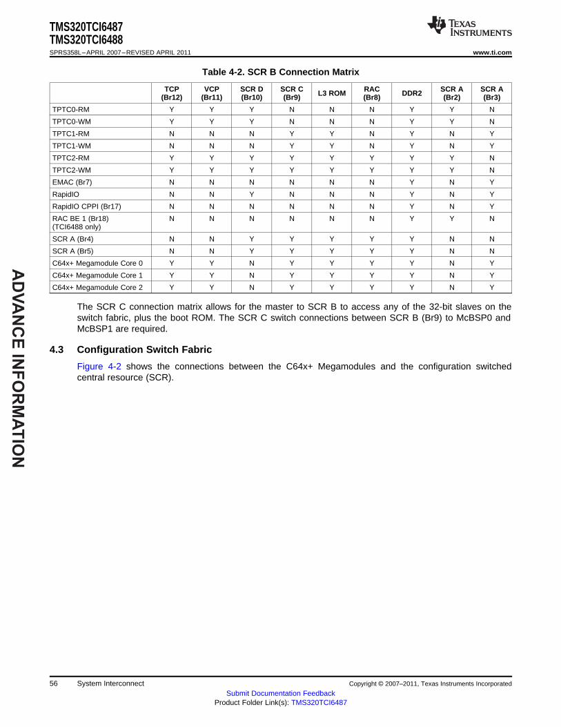
AD
VA
NC
E IN
FO
RM
AT
ION
TMS320TCI6487TMS320TCI6488SPRS358L–APRIL 2007–REVISED APRIL 2011 www.ti.com
Table 4-2. SCR B Connection Matrix
TCP VCP SCR D SCR C RAC SCR A SCR AL3 ROM DDR2(Br12) (Br11) (Br10) (Br9) (Br8) (Br2) (Br3)
TPTC0-RM Y Y Y N N N Y Y N
TPTC0-WM Y Y Y N N N Y Y N
TPTC1-RM N N N Y Y N Y N Y
TPTC1-WM N N N Y Y N Y N Y
TPTC2-RM Y Y Y Y Y Y Y Y N
TPTC2-WM Y Y Y Y Y Y Y Y N
EMAC (Br7) N N N N N N Y N Y
RapidIO N N Y N N N Y N Y
RapidIO CPPI (Br17) N N N N N N Y N Y
RAC BE 1 (Br18) N N N N N N Y Y N(TCI6488 only)
SCR A (Br4) N N Y Y Y Y Y N N
SCR A (Br5) N N Y Y Y Y Y N N
C64x+ Megamodule Core 0 Y Y N Y Y Y Y N Y
C64x+ Megamodule Core 1 Y Y N Y Y Y Y N Y
C64x+ Megamodule Core 2 Y Y N Y Y Y Y N Y
The SCR C connection matrix allows for the master to SCR B to access any of the 32-bit slaves on theswitch fabric, plus the boot ROM. The SCR C switch connections between SCR B (Br9) to McBSP0 andMcBSP1 are required.
4.3 Configuration Switch Fabric
Figure 4-2 shows the connections between the C64x+ Megamodules and the configuration switchedcentral resource (SCR).
56 System Interconnect Copyright © 2007–2011, Texas Instruments Incorporated
Submit Documentation FeedbackProduct Folder Link(s): TMS320TCI6487
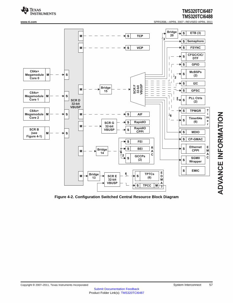
AD
VA
NC
E I
NF
OR
MA
TIO
NS
S
M
M
S
M S
M
S
M
S
M S
M
S
S
S
S
S
S
TCP
VCP S
S
S
S
S
S
S
S
S
S
2
6
2
2
6
S
SM
M
S
3
S
S
M
M
M
C64x+Megamodule
Core 0
C64x+Megamodule
Core 1
SCR B(see
Figure 4-1)
C64x+Megamodule
Core 2
SCR D32-bit
VBUSP
Bridge15
SC
R F
32-b
itV
BU
SP
SCR G32-bit
VBUSP
AIF
RapidIO
RapidIOCPPI
S
Bridge14
Bridge13
SCR E32-bit
VBUSP
FEI
BEI
GCCPs(2)
RAC
TPTCs(6)
EDMA3TPCC
Bridge20
ETB (3)
Semaphore
FSYNC
CFGC/CIC/DTF
GPIO
SMcBSPs
(2)
I2C
GPSC
PLL Ctrls(2)
TPMGR
Timer64s(6)
Ti
mer
MDIO
CP-GMAC
EthernetCPPI
SGMIIWrapper
EMIC
EMAC
TMS320TCI6487TMS320TCI6488
www.ti.com SPRS358L–APRIL 2007–REVISED APRIL 2011
Figure 4-2. Configuration Switched Central Resource Block Diagram
Copyright © 2007–2011, Texas Instruments Incorporated System Interconnect 57Submit Documentation Feedback
Product Folder Link(s): TMS320TCI6487
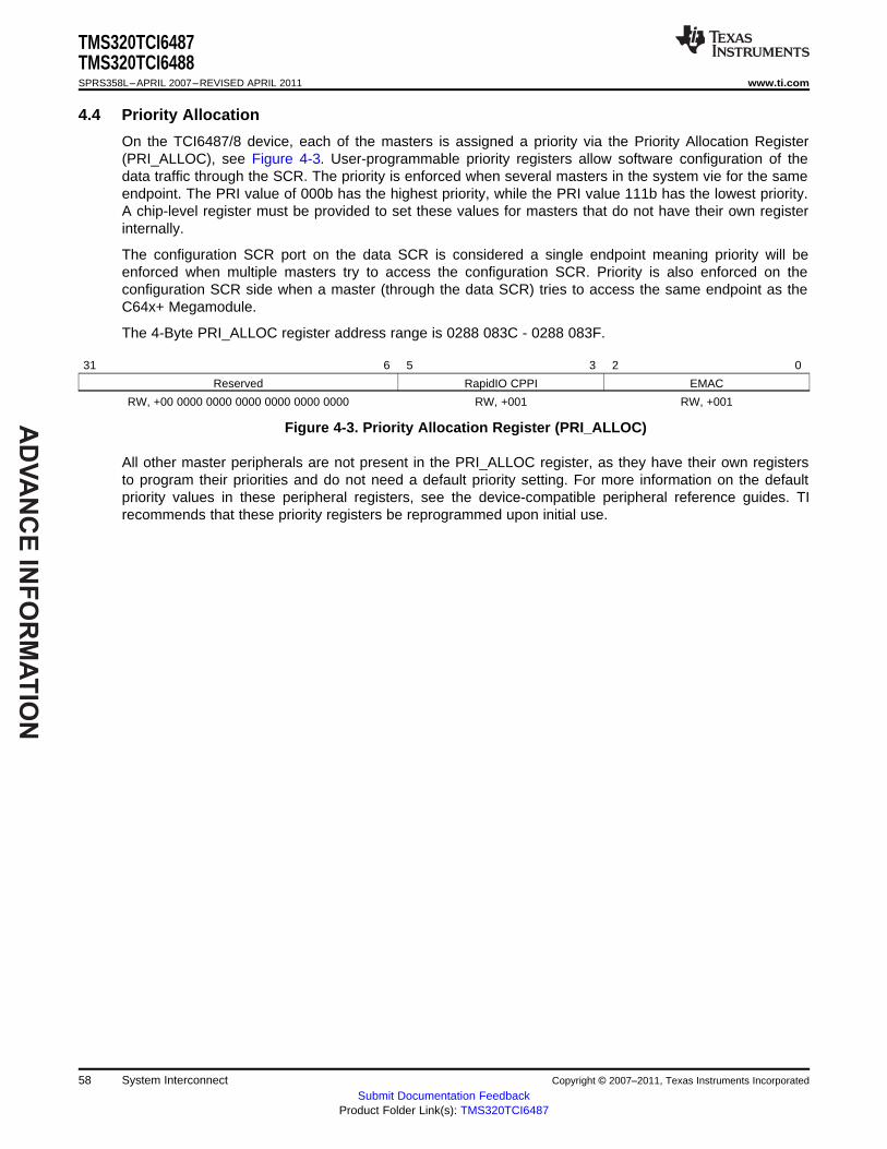
AD
VA
NC
E IN
FO
RM
AT
ION
TMS320TCI6487TMS320TCI6488SPRS358L–APRIL 2007–REVISED APRIL 2011 www.ti.com
4.4 Priority Allocation
On the TCI6487/8 device, each of the masters is assigned a priority via the Priority Allocation Register(PRI_ALLOC), see Figure 4-3. User-programmable priority registers allow software configuration of thedata traffic through the SCR. The priority is enforced when several masters in the system vie for the sameendpoint. The PRI value of 000b has the highest priority, while the PRI value 111b has the lowest priority.A chip-level register must be provided to set these values for masters that do not have their own registerinternally.
The configuration SCR port on the data SCR is considered a single endpoint meaning priority will beenforced when multiple masters try to access the configuration SCR. Priority is also enforced on theconfiguration SCR side when a master (through the data SCR) tries to access the same endpoint as theC64x+ Megamodule.
The 4-Byte PRI_ALLOC register address range is 0288 083C - 0288 083F.
31 6 5 3 2 0
Reserved RapidIO CPPI EMAC
RW, +00 0000 0000 0000 0000 0000 0000 RW, +001 RW, +001
Figure 4-3. Priority Allocation Register (PRI_ALLOC)
All other master peripherals are not present in the PRI_ALLOC register, as they have their own registersto program their priorities and do not need a default priority setting. For more information on the defaultpriority values in these peripheral registers, see the device-compatible peripheral reference guides. TIrecommends that these priority registers be reprogrammed upon initial use.
58 System Interconnect Copyright © 2007–2011, Texas Instruments Incorporated
Submit Documentation FeedbackProduct Folder Link(s): TMS320TCI6487

AD
VA
NC
E I
NF
OR
MA
TIO
N
32KB L1P
Memory Controller (PMC) withMemory Protect/Bandwidth Mgmt
C64x+ DSP Core
Instruction Fetch
16-/32-bit Instruction Dispatch
Control Registers
In-Circuit Emulation
Instruction Decode
Data Path A Data Path B
A31 - A16
A15 - A0
A Register File B Register File
B31 - B16
B15 - B0
BootController
LPSCPLLC
GPSC
.L1 .S1.M1xxxx
.D1 .D2.M2xxxx
.S2 .L2
RSARSA32KB L1D
DMA SwitchFabric
CFG SwitchFabric
L2 Cache/SRAM
512, 1024, or1536 KB
Inte
rru
pt
an
d E
xcep
tio
n C
on
tro
ller
Un
ifie
d M
em
ory
Co
ntr
oller
(UM
C)
Exte
rnal M
em
ory
Co
ntr
oller
(EM
C)
Data Memory Controller (DMC) withMemory Protect/Bandwidth Mgmt
TMS320TCI6487TMS320TCI6488
www.ti.com SPRS358L–APRIL 2007–REVISED APRIL 2011
5 C64x+ Megamodule
5.1 Megamodule Diagram
The C64x+ Megamodule consists of several components - the C64x+ CPU and associated C64x+Megamodule core, level-one and level-two memories (L1P, L1D, L2), RSA accelerator, data traceformatter (DTF), embedded trace buffer (ETB), the interrupt controller, power-down controller, externalmemory controller and a dedicated power/sleep controller (LPSC). The C64x+ Megamodule also providessupport for memory protection and bandwidth management (for resources local to the C64x+Megamodule). Figure 5-1 provides a block diagram of the C64x+ Megamodule.
Figure 5-1. C64x+ Megamodule Block Diagram
Copyright © 2007–2011, Texas Instruments Incorporated C64x+ Megamodule 59Submit Documentation Feedback
Product Folder Link(s): TMS320TCI6487
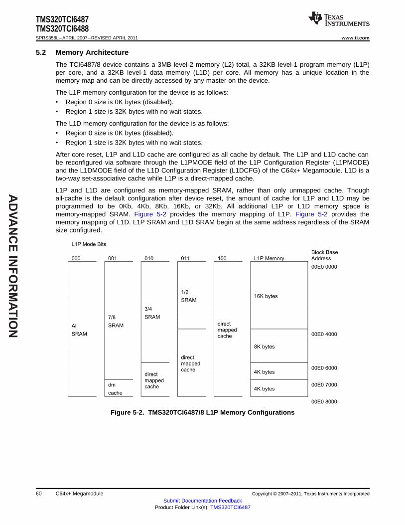
AD
VA
NC
E IN
FO
RM
AT
ION
L1P Mode Bits
000 001 010 011 100 L1P MemoryBlock BaseAddress
00E0 0000
1/2
SRAM16K bytes
00E0 4000
3/4
SRAM
8K bytes
00E0 6000
7/8
SRAM
4K bytes
00E0 7000
All
SRAM
dm
cache
directmappedcache
directmappedcache
directmappedcache
4K bytes
00E0 8000
TMS320TCI6487TMS320TCI6488SPRS358L–APRIL 2007–REVISED APRIL 2011 www.ti.com
5.2 Memory Architecture
The TCI6487/8 device contains a 3MB level-2 memory (L2) total, a 32KB level-1 program memory (L1P)per core, and a 32KB level-1 data memory (L1D) per core. All memory has a unique location in thememory map and can be directly accessed by any master on the device.
The L1P memory configuration for the device is as follows:• Region 0 size is 0K bytes (disabled).• Region 1 size is 32K bytes with no wait states.
The L1D memory configuration for the device is as follows:• Region 0 size is 0K bytes (disabled).• Region 1 size is 32K bytes with no wait states.
After core reset, L1P and L1D cache are configured as all cache by default. The L1P and L1D cache canbe reconfigured via software through the L1PMODE field of the L1P Configuration Register (L1PMODE)and the L1DMODE field of the L1D Configuration Register (L1DCFG) of the C64x+ Megamodule. L1D is atwo-way set-associative cache while L1P is a direct-mapped cache.
L1P and L1D are configured as memory-mapped SRAM, rather than only unmapped cache. Thoughall-cache is the default configuration after device reset, the amount of cache for L1P and L1D may beprogrammed to be 0Kb, 4Kb, 8Kb, 16Kb, or 32Kb. All additional L1P or L1D memory space ismemory-mapped SRAM. Figure 5-2 provides the memory mapping of L1P. Figure 5-2 provides thememory mapping of L1D. L1P SRAM and L1D SRAM begin at the same address regardless of the SRAMsize configured.
Figure 5-2. TMS320TCI6487/8 L1P Memory Configurations
60 C64x+ Megamodule Copyright © 2007–2011, Texas Instruments Incorporated
Submit Documentation FeedbackProduct Folder Link(s): TMS320TCI6487

AD
VA
NC
E I
NF
OR
MA
TIO
N
L1D Mode Bits
000 001 010 011 100 L1D MemoryBlock BaseAddress
00F0 0000
1/2
SRAM16K bytes
00F0 4000
3/4
SRAM
8K bytes
00F0 6000
7/8
SRAM
4K bytes
00F0 7000
All
SRAM
Cache
Cache
Cache
Cache
4K bytes
00F0 8000
L2 Mode Bits
010 011 100 L2 Memory Block Base Address
00800000
83.33%SRAM
1280K bytes91.67%SRAM
128K bytes 00940000
95.84%SRAM
64K bytes 00960000
32K bytes 00970000Cache4.16%
Cache8.33%
Cache16.67%
0097800032K bytes
000 001
97.92%SRAM
100%AllSRAM
Cache2.08%
TMS320TCI6487TMS320TCI6488
www.ti.com SPRS358L–APRIL 2007–REVISED APRIL 2011
Figure 5-3. TMS320TCI6487/8 L1D Memory Configurations
Each core has 1536K bytes, 1024K bytes, or 512K bytes of local L2 RAM, with up to 256KB configurableas cache. The following figures provide the possible memory maps for each of the local L2. The L2memory is typically shared across the two unified memory access ports (UMAP0 and UMAP1). The L2SRAM begins at the same address regardless of the cache size configured.
Figure 5-4. L2 Memory Configuration 1536KB
Copyright © 2007–2011, Texas Instruments Incorporated C64x+ Megamodule 61Submit Documentation Feedback
Product Folder Link(s): TMS320TCI6487
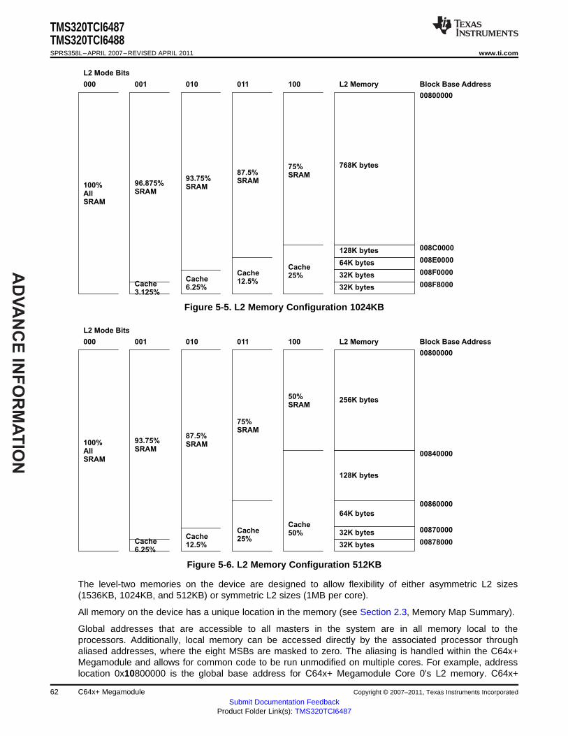
AD
VA
NC
E IN
FO
RM
AT
ION
L2 Mode Bits
010 011 100 L2 Memory Block Base Address
00800000
75%SRAM
768K bytes87.5%SRAM
128K bytes 008C0000
93.75%SRAM
64K bytes 008E0000
32K bytes 008F0000Cache6.25%
Cache12.5%
Cache25%
008F800032K bytes
000 001
96.875%SRAM
100%AllSRAM
Cache3.125%
L2 Mode Bits
010 011 100 L2 Memory Block Base Address
00800000
50%SRAM
256K bytes
75%SRAM
128K bytes
00840000
87.5%SRAM
64K bytes
00860000
32K bytes 00870000Cache12.5%
Cache25%
Cache50%
0087800032K bytes
000 001
93.75%SRAM
100%AllSRAM
Cache6.25%
TMS320TCI6487TMS320TCI6488SPRS358L–APRIL 2007–REVISED APRIL 2011 www.ti.com
Figure 5-5. L2 Memory Configuration 1024KB
Figure 5-6. L2 Memory Configuration 512KB
The level-two memories on the device are designed to allow flexibility of either asymmetric L2 sizes(1536KB, 1024KB, and 512KB) or symmetric L2 sizes (1MB per core).
All memory on the device has a unique location in the memory (see Section 2.3, Memory Map Summary).
Global addresses that are accessible to all masters in the system are in all memory local to theprocessors. Additionally, local memory can be accessed directly by the associated processor throughaliased addresses, where the eight MSBs are masked to zero. The aliasing is handled within the C64x+Megamodule and allows for common code to be run unmodified on multiple cores. For example, addresslocation 0x10800000 is the global base address for C64x+ Megamodule Core 0's L2 memory. C64x+
62 C64x+ Megamodule Copyright © 2007–2011, Texas Instruments Incorporated
Submit Documentation FeedbackProduct Folder Link(s): TMS320TCI6487
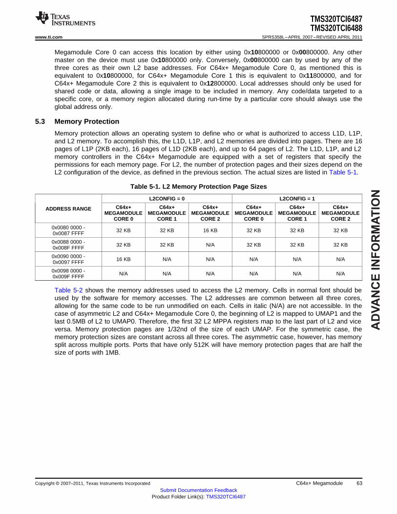
AD
VA
NC
E I
NF
OR
MA
TIO
N
TMS320TCI6487TMS320TCI6488
www.ti.com SPRS358L–APRIL 2007–REVISED APRIL 2011
Megamodule Core 0 can access this location by either using 0x10800000 or 0x00800000. Any othermaster on the device must use 0x10800000 only. Conversely, 0x00800000 can by used by any of thethree cores as their own L2 base addresses. For C64x+ Megamodule Core 0, as mentioned this isequivalent to 0x10800000, for C64x+ Megamodule Core 1 this is equivalent to 0x11800000, and forC64x+ Megamodule Core 2 this is equivalent to 0x12800000. Local addresses should only be used forshared code or data, allowing a single image to be included in memory. Any code/data targeted to aspecific core, or a memory region allocated during run-time by a particular core should always use theglobal address only.
5.3 Memory Protection
Memory protection allows an operating system to define who or what is authorized to access L1D, L1P,and L2 memory. To accomplish this, the L1D, L1P, and L2 memories are divided into pages. There are 16pages of L1P (2KB each), 16 pages of L1D (2KB each), and up to 64 pages of L2. The L1D, L1P, and L2memory controllers in the C64x+ Megamodule are equipped with a set of registers that specify thepermissions for each memory page. For L2, the number of protection pages and their sizes depend on theL2 configuration of the device, as defined in the previous section. The actual sizes are listed in Table 5-1.
Table 5-1. L2 Memory Protection Page Sizes
L2CONFIG = 0 L2CONFIG = 1
C64x+ C64x+ C64x+ C64x+ C64x+ C64x+ADDRESS RANGEMEGAMODULE MEGAMODULE MEGAMODULE MEGAMODULE MEGAMODULE MEGAMODULE
CORE 0 CORE 1 CORE 2 CORE 0 CORE 1 CORE 2
0x0080 0000 - 32 KB 32 KB 16 KB 32 KB 32 KB 32 KB0x0087 FFFF
0x0088 0000 - 32 KB 32 KB N/A 32 KB 32 KB 32 KB0x008F FFFF
0x0090 0000 - 16 KB N/A N/A N/A N/A N/A0x0097 FFFF
0x0098 0000 - N/A N/A N/A N/A N/A N/A0x009F FFFF
Table 5-2 shows the memory addresses used to access the L2 memory. Cells in normal font should beused by the software for memory accesses. The L2 addresses are common between all three cores,allowing for the same code to be run unmodified on each. Cells in italic (N/A) are not accessible. In thecase of asymmetric L2 and C64x+ Megamodule Core 0, the beginning of L2 is mapped to UMAP1 and thelast 0.5MB of L2 to UMAP0. Therefore, the first 32 L2 MPPA registers map to the last part of L2 and viceversa. Memory protection pages are 1/32nd of the size of each UMAP. For the symmetric case, thememory protection sizes are constant across all three cores. The asymmetric case, however, has memorysplit across multiple ports. Ports that have only 512K will have memory protection pages that are half thesize of ports with 1MB.
Copyright © 2007–2011, Texas Instruments Incorporated C64x+ Megamodule 63Submit Documentation Feedback
Product Folder Link(s): TMS320TCI6487
AD
VA
NC
E IN
FO
RM
AT
ION
TMS320TCI6487TMS320TCI6488SPRS358L–APRIL 2007–REVISED APRIL 2011 www.ti.com
Table 5-2. L2 Memory Address Ranges
L2_CONFIG = 0 L2_CONFIG = 1
C64x+ C64x+ C64x+ C64x+ C64x+ C64x+ADDRESS RANGEMEGAMODULE MEGAMODULE MEGAMODULE MEGAMODULE MEGAMODULE MEGAMODULE
CORE 0 CORE 1 CORE 2 CORE 0 CORE 1 CORE 2
0x0080 0000 - UMAP 1 UMAP 0 UMAP 0 UMAP 0 UMAP 0 UMAP 00x0087 FFFF
0x0088 0000 - UMAP 1 UMAP 0 N/A UMAP 0 UMAP 0 UMAP 00x008F FFFF
0x0090 0000 - UMAP 0 N/A N/A N/A N/A N/A0x0097 FFFF
0x0098 0000 - N/A N/A N/A N/A N/A N/A0x009F FFFF
Each page may be assigned with fully orthogonal user and supervisor read, write, and executepermissions. Additionally, a page may be marked as either (or both) locally or globally accessible. A localaccess is one initiated by the CPU, while a global access is initiated by a DMA (either IDMA or DMAaccess by any C64x+ Megamodule or master peripheral).
The CPU and each of the system masters on the device are all assigned a privilege ID (see Table 5-3).The AIDx (x=0,1,2,3,4,5) and LOCAL bits of the memory protection page attribute registers specify thememory page protection scheme as listed in Table 5-4.
Whenever the CPU is the initiator of a memory transaction, the privilege mode (user or supervisor) inwhich the CPU is running at that time is carried with those transactions. This includes EDMA3 transfersthat are programmed by the CPU. Other system masters (EMAC, RapidIO, RAC (TCI6488 only)) arealways in user mode.
64 C64x+ Megamodule Copyright © 2007–2011, Texas Instruments Incorporated
Submit Documentation FeedbackProduct Folder Link(s): TMS320TCI6487
AD
VA
NC
E I
NF
OR
MA
TIO
N
TMS320TCI6487TMS320TCI6488
www.ti.com SPRS358L–APRIL 2007–REVISED APRIL 2011
Table 5-3. Available Memory Page Protection Scheme with Privilege ID
PRIVID MODULE PRIVILEGE MODE DESCRIPTION
0 Inherited from CPU (1) C64x+ Megamodule Core 0
1 Inherited from CPU (1) C64x+ Megamodule Core 1
2 Inherited from CPU (1) C64x+ Megamodule Core 2
3 User EMAC
4 User RapidIO and RapidIO CPPI
5 User RAC BE0 and RAC BE1 (TCI6488 only)
(1) Also applies to EDMA3 transfers that are programmed by the CPU.
Table 5-4. Available Memory Page Protection Scheme with AIDx and Local Bits
AIDx BIT LOCAL BIT DESCRIPTION(x=0,1,2,3,4,5)
0 0 No access to memory page is permitted.
0 1 Only direct access by CPU is permitted
Only accesses by system masters and IDMA are permitted (includes EDMA and IDMA1 0 accesses initiated by the CPU)
1 1 All accesses permitted
Faults are handled by software in an interrupt (or exception, programmable within each C64x+Megamodule interrupt controller) service routine. A CPU or DMA access to a page without the properpermissions will:• Block the access - reads return zero, writes are voided.• Capture the initiator in a status register - ID, address, and access type are stored.• Signal event to CPU interrupt controller.
The software is responsible for taking corrective action to respond to the event and resetting the errorstatus in the memory controller.
5.4 Bandwidth Management
When multiple requesters contend for a single C64x+ Megamodule resource, the conflict is solved bygranting access to the highest priority requestor. The following four resources are managed by theBandwidth Management control hardware:• Level 1 Program (L1P) SRAM/Cache• Level 1 Data (L1D) SRAM/Cache• Level 2 (L2) SRAM/Cache• Memory-mapped registers configuration bus
The priority level for operations initiated within the C64x+ Megamodule; e.g., CPU-initiated transfers,user-programmed cache coherency operations, and IDMA-initiated transfers, are declared throughregisters in the C64x+ Megamodule. The priority level for operations initiated outside the C64x+Megamodule by system peripherals is declared through the Priority Allocation Register (PRI_ALLOC), seeSection 4.4. System peripherals with no fields in PRI_ALLOC have their own registers to program theirpriorities.
Table 5-5 shows the default priorities of all masters in the device.
Copyright © 2007–2011, Texas Instruments Incorporated C64x+ Megamodule 65Submit Documentation Feedback
Product Folder Link(s): TMS320TCI6487

AD
VA
NC
E IN
FO
RM
AT
ION
TMS320TCI6487TMS320TCI6488SPRS358L–APRIL 2007–REVISED APRIL 2011 www.ti.com
Table 5-5. TCI6487/8 Default Master Priorities
DEFAULT MASTER PRIORITIESMASTER (0 = Highest priority, PRIORITY CONTROL
7 = Lowest priority)
EDMA3TCx 0 QUEPRI.PRIQx (EDMA3 register)
SRIO (Data Access) 0 PER_SET_CNTL.CBA_TRANS_PRI (SRIOregister)
SRIO (Descriptor Access) 1 PRI_ALLOC.SRIO_CPPI
EMAC 1 PRI_ALLOC.EMAC
RAC Back-End (TCI6488 only) 7 RAC register
C64x+ Megamodule (MDMA port) 7 MDMAARBE.PRI (C64x+ Megamoduleregister)
C64x+ Megamodule (CPU Arbitration control 1 CPUARBU (C64x+ Megamodule register)to L2)
C64x+ Megamodule (IDMA channel 1) 0 IDMA1_COUNT (C64x+ Megamoduleregister)
5.5 Power-Down Control
The C64x+ Megamodule supports the ability to power-down various parts of the C64x+ Megamodule. Thepower-down controller (PDC) of the C64x+ Megamodule can be used to power down L1P, the cachecontrol hardware, the CPU, and the entire C64x+ Megamodule. These power-down features can be usedto design systems for lower overall system power requirements. Note that the device does not supportpower-down modes for the L2 memory at this time.
5.6 Megamodule Resets
Table 5-6 shows the reset types supported on the device and if the resetting affects the Megamoduleglobally or just locally.
Table 5-6. Megamodule Reset (Global or Local)
RESET TYPE GLOBAL RESET LOCAL RESET
Power-On Y Y
Warm Y Y
System Y Y
CPU N Y
5.7 Megamodule Revision
The version and revision of the C64x+ Megamodule can be read from the Megamodule Revision IDRegister (MM_REVID) located at address 0181 2000h. The MM_REVID register is shown in Figure 5-7and described in Table 5-7. The C64x+ Megamodule revision is dependant on the silicon revision beingused.
Figure 5-7. Megamodule Revision ID Register (MM_REVID) [Hex Address: 0181 2000h]
31 16 15 0
VERSION REVISION (1)
R-3h R-n
LEGEND: R/W = Read/Write; R = Read only; -n = value after reset
(1) The C64x+ Megamodule revision is dependent on the silicon revision being used.
66 C64x+ Megamodule Copyright © 2007–2011, Texas Instruments Incorporated
Submit Documentation FeedbackProduct Folder Link(s): TMS320TCI6487

AD
VA
NC
E I
NF
OR
MA
TIO
N
TMS320TCI6487TMS320TCI6488
www.ti.com SPRS358L–APRIL 2007–REVISED APRIL 2011
Table 5-7. Megamodule Revision ID Register (MM_REVID) Field Descriptions
BIT FIELD VALUE DESCRIPTION
31:16 VERSION 3H Version of the C64x+ Megamodule implemented on the device. This field is always read as 3h.
15:0 REVISION Revision of the C64x+ Megamodule version implemented on the device. The C64x+ Megamodulerevision is dependent on the silicon revision being used.
5.8 C64X+ Megamodule Register Description(s)
In some applications, some specific addresses may need to be read from their physical locations eachtime they are accessed (e.g., a status register within FPGA).
The L2 controller offers registers that control whether certain ranges of memory are cacheable andwhether one or more requestors are actually permitted to access these ranges. The registers are referredto as memory attribute registers (MARs). A list of MARs is provided in Table 5-12.
Table 5-8. Megamodule Interrupt Registers
HEX ADDRESS ACRONYM REGISTER NAME
0180 0000 EVTFLAG0 Event Flag Register 0 (Events [31:0])
0180 0004 EVTFLAG1 Event Flag Register 1
0180 0008 EVTFLAG2 Event Flag Register 2
0180 000C EVTFLAG3 Event Flag Register 3
0180 0010 - 0180 001C - Reserved
0180 0020 EVTSET0 Event Set Register 0 (Events [31:0])
0180 0024 EVTSET1 Event Set Register 1
0180 0028 EVTSET2 Event Set Register 2
0180 002C EVTSET3 Event Set Register 3
0180 0030 - 0180 003C - Reserved
0180 0040 EVTCLR0 Event Clear Register 0 (Events [31:0])
0180 0044 EVTCLR1 Event Clear Register 1
0180 0048 EVTCLR2 Event Clear Register 2
0180 004C EVTCLR3 Event Clear Register 3
0180 0050 - 0180 007C - Reserved
0180 0080 EVTMASK0 Event Mask Register 0 (Events [31:0])
0180 0084 EVTMASK1 Event Mask Register 1
0180 0088 EVTMASK2 Event Mask Register 2
0180 008C EVTMASK3 Event Mask Register 3
0180 0090 - 0180 009C - Reserved
0180 00A0 MEVFLAG0 Masked Event Flag Status Register 0 (Events [31:0])
0180 00A4 MEVFLAG1 Masked Event Flag Status Register 1
0180 00A8 MEVFLAG2 Masked Event Flag Status Register 2
0180 00AC MEVFLAG3 Masked Event Flag Status Register 3
0180 00B0 - 0180 00BC - Reserved
0180 00C0 EXPMASK0 Exception Mask Register 0 (Events [31:0])
0180 00C4 EXPMASK1 Exception Mask Register 1
0180 00C8 EXPMASK2 Exception Mask Register 2
0180 00CC EXPMASK3 Exception Mask Register 3
0180 00D0 - 0180 00DC - Reserved
0180 00E0 MEXPFLAG0 Masked Exception Flag Register 0(Events [31:0])
0180 00E4 MEXPFLAG1 Masked Exception Flag Register 1
0180 00E8 MEXPFLAG2 Masked Exception Flag Register 2
0180 00EC MEXPFLAG3 Masked Exception Flag Register 3
Copyright © 2007–2011, Texas Instruments Incorporated C64x+ Megamodule 67Submit Documentation Feedback
Product Folder Link(s): TMS320TCI6487

AD
VA
NC
E IN
FO
RM
AT
ION
TMS320TCI6487TMS320TCI6488SPRS358L–APRIL 2007–REVISED APRIL 2011 www.ti.com
Table 5-8. Megamodule Interrupt Registers (continued)
HEX ADDRESS ACRONYM REGISTER NAME
0180 00F0 - 0180 00FC - Reserved
0180 0100 - Reserved
0180 0104 INTMUX1 Interrupt Multiplexer Register 1
0180 0108 INTMUX2 Interrupt Multiplexer Register 2
0180 010C INTMUX3 Interrupt Multiplexer Register 3
0180 0110 - 0180 013C - Reserved
0180 0140 AEGMUX0 Advanced Event Generator Mux Register 0
0180 0144 AEGMUX1 Advanced Event Generator Mux Register 1
0180 0148 - 0180 017C - Reserved
0180 0180 INTXSTAT Interrupt Exception Status Register
0180 0184 INTXCLER Interrupt Exception Clear Register
0180 0188 INTDMASK Dropped Interrupt Mask Register
0180 0188 - 0180 01BC - Reserved
0180 01C0 EVTASRT Event Asserting Register (boot complete register) (1)
0180 01C4 - 0180 FFFF - Reserved
(1) Only bit 4 is used, all other bits are reserved. Bit 4 is write only and has the default 0. After boot is complete, bit 4 is set to 1 and Cores1 and 2 are released out of reset and start executing their codes.
Table 5-9. Megamodule Power-Down Control Registers
HEX ADDRESS ACRONYM REGISTER NAME
0181 0000 PDCCMD Power-Down Controller Command Register
0181 0004 - 0181 1FFF - Reserved
Table 5-10. Megamodule Revision Register
HEX ADDRESS ACRONYM REGISTER NAME
0181 2000 MM_REVID Megamodule Revision ID Register
0181 2004 - 0181 2FFF - Reserved
Table 5-11. Megamodule IDMA Registers
HEX ADDRESS ACRONYM REGISTER NAME
0182 0000 IDMA0STAT IDMA Channel 0 Status Register
0182 0004 IDMA0MASK IDMA Channel 0 Mask Register
0182 0008 IDMA0SCR IDMA Channel 0 Source Address Register
0182 000C IDMA0DST IDMA Channel 0 Destination Address Register
0182 0010 IDMA0CNT IDMA Channel 0 Count Register
0182 0014 - 0182 00FC - Reserved
0182 0100 IDMA1STAT IDMA Channel 1 Status Register
0182 0104 - Reserved
0182 0108 IDMA1SRC IDMA Channel 1 Source Address Register
0182 010C IDMA1DST IDMA Channel 1 Destination Address Register
0182 0110 IDMA1CNT IDMA Channel 1 Count Register
0182 0114 - 0182 017C - Reserved
0182 0180 - Reserved
0182 0184 - 0182 01FC - Reserved
68 C64x+ Megamodule Copyright © 2007–2011, Texas Instruments Incorporated
Submit Documentation FeedbackProduct Folder Link(s): TMS320TCI6487
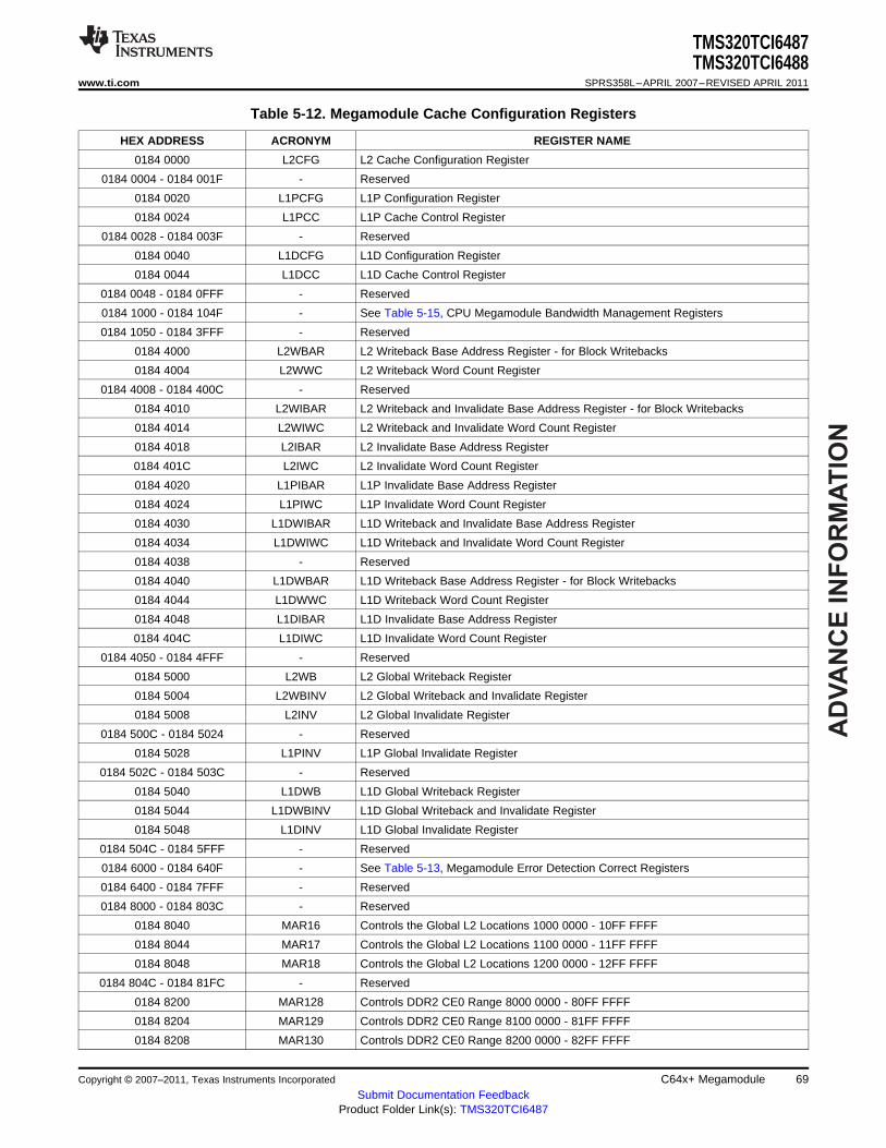
AD
VA
NC
E I
NF
OR
MA
TIO
N
TMS320TCI6487TMS320TCI6488
www.ti.com SPRS358L–APRIL 2007–REVISED APRIL 2011
Table 5-12. Megamodule Cache Configuration Registers
HEX ADDRESS ACRONYM REGISTER NAME
0184 0000 L2CFG L2 Cache Configuration Register
0184 0004 - 0184 001F - Reserved
0184 0020 L1PCFG L1P Configuration Register
0184 0024 L1PCC L1P Cache Control Register
0184 0028 - 0184 003F - Reserved
0184 0040 L1DCFG L1D Configuration Register
0184 0044 L1DCC L1D Cache Control Register
0184 0048 - 0184 0FFF - Reserved
0184 1000 - 0184 104F - See Table 5-15, CPU Megamodule Bandwidth Management Registers
0184 1050 - 0184 3FFF - Reserved
0184 4000 L2WBAR L2 Writeback Base Address Register - for Block Writebacks
0184 4004 L2WWC L2 Writeback Word Count Register
0184 4008 - 0184 400C - Reserved
0184 4010 L2WIBAR L2 Writeback and Invalidate Base Address Register - for Block Writebacks
0184 4014 L2WIWC L2 Writeback and Invalidate Word Count Register
0184 4018 L2IBAR L2 Invalidate Base Address Register
0184 401C L2IWC L2 Invalidate Word Count Register
0184 4020 L1PIBAR L1P Invalidate Base Address Register
0184 4024 L1PIWC L1P Invalidate Word Count Register
0184 4030 L1DWIBAR L1D Writeback and Invalidate Base Address Register
0184 4034 L1DWIWC L1D Writeback and Invalidate Word Count Register
0184 4038 - Reserved
0184 4040 L1DWBAR L1D Writeback Base Address Register - for Block Writebacks
0184 4044 L1DWWC L1D Writeback Word Count Register
0184 4048 L1DIBAR L1D Invalidate Base Address Register
0184 404C L1DIWC L1D Invalidate Word Count Register
0184 4050 - 0184 4FFF - Reserved
0184 5000 L2WB L2 Global Writeback Register
0184 5004 L2WBINV L2 Global Writeback and Invalidate Register
0184 5008 L2INV L2 Global Invalidate Register
0184 500C - 0184 5024 - Reserved
0184 5028 L1PINV L1P Global Invalidate Register
0184 502C - 0184 503C - Reserved
0184 5040 L1DWB L1D Global Writeback Register
0184 5044 L1DWBINV L1D Global Writeback and Invalidate Register
0184 5048 L1DINV L1D Global Invalidate Register
0184 504C - 0184 5FFF - Reserved
0184 6000 - 0184 640F - See Table 5-13, Megamodule Error Detection Correct Registers
0184 6400 - 0184 7FFF - Reserved
0184 8000 - 0184 803C - Reserved
0184 8040 MAR16 Controls the Global L2 Locations 1000 0000 - 10FF FFFF
0184 8044 MAR17 Controls the Global L2 Locations 1100 0000 - 11FF FFFF
0184 8048 MAR18 Controls the Global L2 Locations 1200 0000 - 12FF FFFF
0184 804C - 0184 81FC - Reserved
0184 8200 MAR128 Controls DDR2 CE0 Range 8000 0000 - 80FF FFFF
0184 8204 MAR129 Controls DDR2 CE0 Range 8100 0000 - 81FF FFFF
0184 8208 MAR130 Controls DDR2 CE0 Range 8200 0000 - 82FF FFFF
Copyright © 2007–2011, Texas Instruments Incorporated C64x+ Megamodule 69Submit Documentation Feedback
Product Folder Link(s): TMS320TCI6487
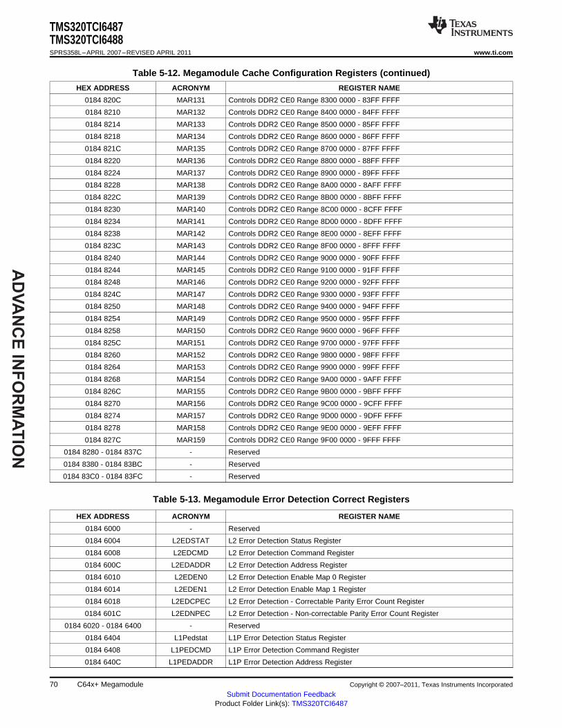
AD
VA
NC
E IN
FO
RM
AT
ION
TMS320TCI6487TMS320TCI6488SPRS358L–APRIL 2007–REVISED APRIL 2011 www.ti.com
Table 5-12. Megamodule Cache Configuration Registers (continued)
HEX ADDRESS ACRONYM REGISTER NAME
0184 820C MAR131 Controls DDR2 CE0 Range 8300 0000 - 83FF FFFF
0184 8210 MAR132 Controls DDR2 CE0 Range 8400 0000 - 84FF FFFF
0184 8214 MAR133 Controls DDR2 CE0 Range 8500 0000 - 85FF FFFF
0184 8218 MAR134 Controls DDR2 CE0 Range 8600 0000 - 86FF FFFF
0184 821C MAR135 Controls DDR2 CE0 Range 8700 0000 - 87FF FFFF
0184 8220 MAR136 Controls DDR2 CE0 Range 8800 0000 - 88FF FFFF
0184 8224 MAR137 Controls DDR2 CE0 Range 8900 0000 - 89FF FFFF
0184 8228 MAR138 Controls DDR2 CE0 Range 8A00 0000 - 8AFF FFFF
0184 822C MAR139 Controls DDR2 CE0 Range 8B00 0000 - 8BFF FFFF
0184 8230 MAR140 Controls DDR2 CE0 Range 8C00 0000 - 8CFF FFFF
0184 8234 MAR141 Controls DDR2 CE0 Range 8D00 0000 - 8DFF FFFF
0184 8238 MAR142 Controls DDR2 CE0 Range 8E00 0000 - 8EFF FFFF
0184 823C MAR143 Controls DDR2 CE0 Range 8F00 0000 - 8FFF FFFF
0184 8240 MAR144 Controls DDR2 CE0 Range 9000 0000 - 90FF FFFF
0184 8244 MAR145 Controls DDR2 CE0 Range 9100 0000 - 91FF FFFF
0184 8248 MAR146 Controls DDR2 CE0 Range 9200 0000 - 92FF FFFF
0184 824C MAR147 Controls DDR2 CE0 Range 9300 0000 - 93FF FFFF
0184 8250 MAR148 Controls DDR2 CE0 Range 9400 0000 - 94FF FFFF
0184 8254 MAR149 Controls DDR2 CE0 Range 9500 0000 - 95FF FFFF
0184 8258 MAR150 Controls DDR2 CE0 Range 9600 0000 - 96FF FFFF
0184 825C MAR151 Controls DDR2 CE0 Range 9700 0000 - 97FF FFFF
0184 8260 MAR152 Controls DDR2 CE0 Range 9800 0000 - 98FF FFFF
0184 8264 MAR153 Controls DDR2 CE0 Range 9900 0000 - 99FF FFFF
0184 8268 MAR154 Controls DDR2 CE0 Range 9A00 0000 - 9AFF FFFF
0184 826C MAR155 Controls DDR2 CE0 Range 9B00 0000 - 9BFF FFFF
0184 8270 MAR156 Controls DDR2 CE0 Range 9C00 0000 - 9CFF FFFF
0184 8274 MAR157 Controls DDR2 CE0 Range 9D00 0000 - 9DFF FFFF
0184 8278 MAR158 Controls DDR2 CE0 Range 9E00 0000 - 9EFF FFFF
0184 827C MAR159 Controls DDR2 CE0 Range 9F00 0000 - 9FFF FFFF
0184 8280 - 0184 837C - Reserved
0184 8380 - 0184 83BC - Reserved
0184 83C0 - 0184 83FC - Reserved
Table 5-13. Megamodule Error Detection Correct Registers
HEX ADDRESS ACRONYM REGISTER NAME
0184 6000 - Reserved
0184 6004 L2EDSTAT L2 Error Detection Status Register
0184 6008 L2EDCMD L2 Error Detection Command Register
0184 600C L2EDADDR L2 Error Detection Address Register
0184 6010 L2EDEN0 L2 Error Detection Enable Map 0 Register
0184 6014 L2EDEN1 L2 Error Detection Enable Map 1 Register
0184 6018 L2EDCPEC L2 Error Detection - Correctable Parity Error Count Register
0184 601C L2EDNPEC L2 Error Detection - Non-correctable Parity Error Count Register
0184 6020 - 0184 6400 - Reserved
0184 6404 L1Pedstat L1P Error Detection Status Register
0184 6408 L1PEDCMD L1P Error Detection Command Register
0184 640C L1PEDADDR L1P Error Detection Address Register
70 C64x+ Megamodule Copyright © 2007–2011, Texas Instruments Incorporated
Submit Documentation FeedbackProduct Folder Link(s): TMS320TCI6487

AD
VA
NC
E I
NF
OR
MA
TIO
N
TMS320TCI6487TMS320TCI6488
www.ti.com SPRS358L–APRIL 2007–REVISED APRIL 2011
Table 5-14. Megamodule L1/L2 Memory Protection Registers
HEX ADDRESS ACRONYM REGISTER NAME
0184 A000 L2MPFAR L2 Memory Protection Fault Address Register
0184 A004 L2MPFSR L2 Memory Protection Fault Status Register
0184 A008 L2MPFCR L2 memory protection Fault Command Register
0184 A00C - 0184 A0FF - Reserved
0184 A100 L2MPLKO L2 Memory Protection Lock Key Bits [31:0]
0184 A104 L2MPLK1 L2 Memory Protection Lock Key Bits [63:32]
0184 A108 L2MPLK2 L2 Memory Protection Lock Key Bits [95:64]
0184 A10C L2MPLK3 L2 Memory Protection Lock Key Bits [127:96]
0184 A110 L2MPLKCMD L2 Memory Protection Lock Key Command Register
0184 A114 L2MPLKSTAT L2 Memory Protection Lock Key Status Register
0184 A118 - 0184 A1FF - Reserved
0184 A200 L2MPPA0 L2 Memory Protection Page Attribute Register 0 (1)
0184 A204 L2MPPA1 L2 Memory Protection Page Attribute Register 1
0184 A208 L2MPPA2 L2 Memory Protection Page Attribute Register 2
0184 A20C L2MPPA3 L2 Memory Protection Page Attribute Register 3
0184 A210 L2MPPA4 L2 Memory Protection Page Attribute Register 4
0184 A214 L2MPPA5 L2 Memory Protection Page Attribute Register 5
0184 A218 L2MPPA6 L2 Memory Protection Page Attribute Register 6
0184 A21C L2MPPA7 L2 Memory Protection Page Attribute Register 7
0184 A220 L2MPPA8 L2 Memory Protection Page Attribute Register 8
0184 A224 L2MPPA9 L2 Memory Protection Page Attribute Register 9
0184 A228 L2MPPA10 L2 Memory Protection Page Attribute Register 10
0184 A22C L2MPPA11 L2 Memory Protection Page Attribute Register 11
0184 A230 L2MPPA12 L2 Memory Protection Page Attribute Register 12
0184 A234 L2MPPA13 L2 Memory Protection Page Attribute Register 13
0184 A238 L2MPPA14 L2 Memory Protection Page Attribute Register 14
0184 A23C L2MPPA15 L2 Memory Protection Page Attribute Register 15
0184 A240 L2MPPA16 L2 Memory Protection Page Attribute Register 16
0184 A244 L2MPPA17 L2 Memory Protection Page Attribute Register 17
0184 A248 L2MPPA18 L2 Memory Protection Page Attribute Register 18
0184 A24C L2MPPA19 L2 Memory Protection Page Attribute Register 19
0184 A250 L2MPPA20 L2 Memory Protection Page Attribute Register 20
0184 A254 L2MPPA21 L2 Memory Protection Page Attribute Register 21
0184 A258 L2MPPA22 L2 Memory Protection Page Attribute Register 22
0184 A25C L2MPPA23 L2 Memory Protection Page Attribute Register 23
0184 A260 L2MPPA24 L2 Memory Protection Page Attribute Register 24
0184 A264 L2MPPA25 L2 Memory Protection Page Attribute Register 25
0184 A268 L2MPPA26 L2 Memory Protection Page Attribute Register 26
0184 A26C L2MPPA27 L2 Memory Protection Page Attribute Register 27
0184 A270 L2MPPA28 L2 Memory Protection Page Attribute Register 28
0184 A274 L2MPPA29 L2 Memory Protection Page Attribute Register 29
0184 A278 L2MPPA30 L2 Memory Protection Page Attribute Register 30
0184 A27C L2MPPA31 L2 Memory Protection Page Attribute Register 31
0184 A280 L2MPPA32 L2 Memory Protection Page Attribute Register 32
0184 A284 L2MPPA33 L2 Memory Protection Page Attribute Register 33
0184 A288 L2MPPA34 L2 Memory Protection Page Attribute Register 34
(1) The default value of all L2MPPAn registers is 0x0000 FFFF.
Copyright © 2007–2011, Texas Instruments Incorporated C64x+ Megamodule 71Submit Documentation Feedback
Product Folder Link(s): TMS320TCI6487
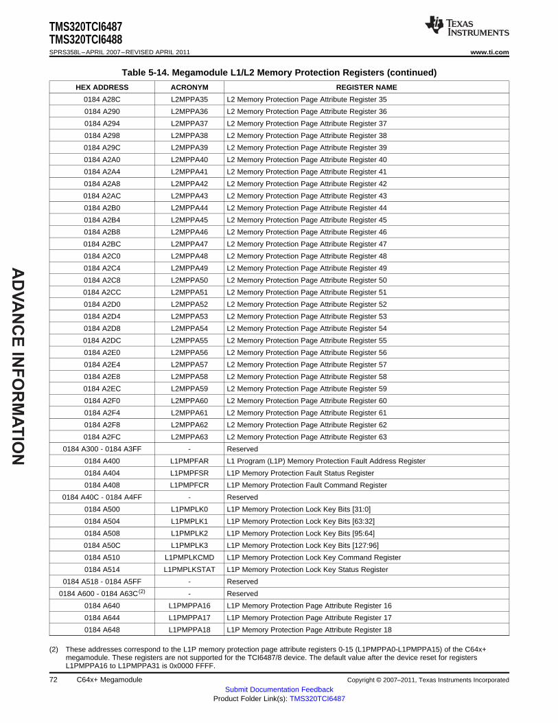
AD
VA
NC
E IN
FO
RM
AT
ION
TMS320TCI6487TMS320TCI6488SPRS358L–APRIL 2007–REVISED APRIL 2011 www.ti.com
Table 5-14. Megamodule L1/L2 Memory Protection Registers (continued)
HEX ADDRESS ACRONYM REGISTER NAME
0184 A28C L2MPPA35 L2 Memory Protection Page Attribute Register 35
0184 A290 L2MPPA36 L2 Memory Protection Page Attribute Register 36
0184 A294 L2MPPA37 L2 Memory Protection Page Attribute Register 37
0184 A298 L2MPPA38 L2 Memory Protection Page Attribute Register 38
0184 A29C L2MPPA39 L2 Memory Protection Page Attribute Register 39
0184 A2A0 L2MPPA40 L2 Memory Protection Page Attribute Register 40
0184 A2A4 L2MPPA41 L2 Memory Protection Page Attribute Register 41
0184 A2A8 L2MPPA42 L2 Memory Protection Page Attribute Register 42
0184 A2AC L2MPPA43 L2 Memory Protection Page Attribute Register 43
0184 A2B0 L2MPPA44 L2 Memory Protection Page Attribute Register 44
0184 A2B4 L2MPPA45 L2 Memory Protection Page Attribute Register 45
0184 A2B8 L2MPPA46 L2 Memory Protection Page Attribute Register 46
0184 A2BC L2MPPA47 L2 Memory Protection Page Attribute Register 47
0184 A2C0 L2MPPA48 L2 Memory Protection Page Attribute Register 48
0184 A2C4 L2MPPA49 L2 Memory Protection Page Attribute Register 49
0184 A2C8 L2MPPA50 L2 Memory Protection Page Attribute Register 50
0184 A2CC L2MPPA51 L2 Memory Protection Page Attribute Register 51
0184 A2D0 L2MPPA52 L2 Memory Protection Page Attribute Register 52
0184 A2D4 L2MPPA53 L2 Memory Protection Page Attribute Register 53
0184 A2D8 L2MPPA54 L2 Memory Protection Page Attribute Register 54
0184 A2DC L2MPPA55 L2 Memory Protection Page Attribute Register 55
0184 A2E0 L2MPPA56 L2 Memory Protection Page Attribute Register 56
0184 A2E4 L2MPPA57 L2 Memory Protection Page Attribute Register 57
0184 A2E8 L2MPPA58 L2 Memory Protection Page Attribute Register 58
0184 A2EC L2MPPA59 L2 Memory Protection Page Attribute Register 59
0184 A2F0 L2MPPA60 L2 Memory Protection Page Attribute Register 60
0184 A2F4 L2MPPA61 L2 Memory Protection Page Attribute Register 61
0184 A2F8 L2MPPA62 L2 Memory Protection Page Attribute Register 62
0184 A2FC L2MPPA63 L2 Memory Protection Page Attribute Register 63
0184 A300 - 0184 A3FF - Reserved
0184 A400 L1PMPFAR L1 Program (L1P) Memory Protection Fault Address Register
0184 A404 L1PMPFSR L1P Memory Protection Fault Status Register
0184 A408 L1PMPFCR L1P Memory Protection Fault Command Register
0184 A40C - 0184 A4FF - Reserved
0184 A500 L1PMPLK0 L1P Memory Protection Lock Key Bits [31:0]
0184 A504 L1PMPLK1 L1P Memory Protection Lock Key Bits [63:32]
0184 A508 L1PMPLK2 L1P Memory Protection Lock Key Bits [95:64]
0184 A50C L1PMPLK3 L1P Memory Protection Lock Key Bits [127:96]
0184 A510 L1PMPLKCMD L1P Memory Protection Lock Key Command Register
0184 A514 L1PMPLKSTAT L1P Memory Protection Lock Key Status Register
0184 A518 - 0184 A5FF - Reserved
0184 A600 - 0184 A63C (2) - Reserved
0184 A640 L1PMPPA16 L1P Memory Protection Page Attribute Register 16
0184 A644 L1PMPPA17 L1P Memory Protection Page Attribute Register 17
0184 A648 L1PMPPA18 L1P Memory Protection Page Attribute Register 18
(2) These addresses correspond to the L1P memory protection page attribute registers 0-15 (L1PMPPA0-L1PMPPA15) of the C64x+megamodule. These registers are not supported for the TCI6487/8 device. The default value after the device reset for registersL1PMPPA16 to L1PMPPA31 is 0x0000 FFFF.
72 C64x+ Megamodule Copyright © 2007–2011, Texas Instruments Incorporated
Submit Documentation FeedbackProduct Folder Link(s): TMS320TCI6487

AD
VA
NC
E I
NF
OR
MA
TIO
N
TMS320TCI6487TMS320TCI6488
www.ti.com SPRS358L–APRIL 2007–REVISED APRIL 2011
Table 5-14. Megamodule L1/L2 Memory Protection Registers (continued)
HEX ADDRESS ACRONYM REGISTER NAME
0184 A64C L1PMPPA19 L1P Memory Protection Page Attribute Register 19
0184 A650 L1PMPPA20 L1P Memory Protection Page Attribute Register 20
0184 A654 L1PMPPA21 L1P Memory Protection Page Attribute Register 21
0184 A658 L1PMPPA22 L1P Memory Protection Page Attribute Register 22
0184 A65C L1PMPPA23 L1P Memory Protection Page Attribute Register 23
0184 A660 L1PMPPA24 L1P Memory Protection Page Attribute Register 24
0184 A664 L1PMPPA25 L1P Memory Protection Page Attribute Register 25
0184 A668 L1PMPPA26 L1P Memory Protection Page Attribute Register 26
0184 A66C L1PMPPA27 L1P Memory Protection Page Attribute Register 27
0184 A670 L1PMPPA28 L1P Memory Protection Page Attribute Register 28
0184 A674 L1PMPPA29 L1P Memory Protection Page Attribute Register 29
0184 A678 L1PMPPA30 L1P Memory Protection Page Attribute Register 30
0184 A67C L1PMPPA31 L1P Memory Protection Page Attribute Register 31
0184 A680 - 0184 ABFF - Reserved
0184 AC00 L1DMPFAR L1 Data (L1D) Memory Protection Fault Address Register
0184 AC04 L1DMPFSR L1D Memory Protection Fault Status Register
0184 AC08 L1DMPFCR L1D Memory Protection Fault Command Register
0184 AC0C - 0184 ACFF - Reserved
0184 AD00 L1DMPLK0 L1D Memory Protection Lock Key Bits [31:0]
0184 AD04 L1DMPLK1 L1D Memory Protection Lock Key Bits [63:32]
0184 AD08 L1DMPLK2 L1D Memory Protection Lock Key Bits [95:64]
0184 AD0C L1DMPLK3 L1D Memory Protection Lock Key Bits [127:96]
0184 AD10 L1DMPLKCMD L1D Memory Protection Lock Key Command Register
0184 AD14 L1DMPLKSTAT L1D Memory Protection Lock Key Status Register
0184 AD18 - 0184 ADFF - Reserved
0184 AE00 - 0184 AE3C (3) - Reserved
0184 AE40 L1DMPPA16 L1D Memory Protection Page Attribute Register 16
0184 AE44 L1DMPPA17 L1D Memory Protection Page Attribute Register 17
0184 AE48 L1DMPPA18 L1D Memory Protection Page Attribute Register 18
0184 AE4C L1DMPPA19 L1D Memory Protection Page Attribute Register 19
0184 AE50 L1DMPPA20 L1D Memory Protection Page Attribute Register 20
0184 AE54 L1DMPPA21 L1D Memory Protection Page Attribute Register 21
0184 AE58 L1DMPPA22 L1D Memory Protection Page Attribute Register 22
0184 AE5C L1DMPPA23 L1D Memory Protection Page Attribute Register 23
0184 AE60 L1DMPPA24 L1D Memory Protection Page Attribute Register 24
0184 AE64 L1DMPPA25 L1D Memory Protection Page Attribute Register 25
0184 AE68 L1DMPPA26 L1D Memory Protection Page Attribute Register 26
0184 AE6C L1DMPPA27 L1D Memory Protection Page Attribute Register 27
0184 AE70 L1DMPPA28 L1D Memory Protection Page Attribute Register 28
0184 AE74 L1DMPPA29 L1D Memory Protection Page Attribute Register 29
0184 AE78 L1DMPPA30 L1D Memory Protection Page Attribute Register 30
0184 AE7C L1DMPPA31 L1D Memory Protection Page Attribute Register 31
0184 AE80 - 0185 FFFF - Reserved
(3) These addresses correspond to the L1D memory protection page attribute registers 0-15 (L1DMPPA0-L1DMPPA15) of the C64x+megamodule. These registers are not supported for the TCI6487/8 device. The default value after the device reset for registersL1DMPPA16 to L1DMPPA31 is 0x0000 FFF6.
Copyright © 2007–2011, Texas Instruments Incorporated C64x+ Megamodule 73Submit Documentation Feedback
Product Folder Link(s): TMS320TCI6487

AD
VA
NC
E IN
FO
RM
AT
ION
TMS320TCI6487TMS320TCI6488SPRS358L–APRIL 2007–REVISED APRIL 2011 www.ti.com
Table 5-15. CPU Megamodule Bandwidth Management Registers
HEX ADDRESS ACRONYM REGISTER NAME
0182 0200 EMCCPUARBE EMC CPU Arbitration Control Register
0182 0204 EMCIDMAARBE EMC IDMA Arbitration Control Register
0182 0208 EMCSDMAARBE EMC Slave DMA Arbitration Control Register
0182 020C EMCMDMAARBE EMC Master DMA Arbitration Control Register
0182 0210 - 0182 02FF - Reserved
0184 1000 L2DCPUARBU L2D CPU Arbitration Control Register
0184 1004 L2DIDMAARBU L2D IDMA Arbitration Control Register
0184 1008 L2DSDMAARBU L2D Slave DMA Arbitration Control Register
0184 100C L2DUCARBU L2D User Coherence Arbitration Control Register
0184 1010 - 0184 103F - Reserved
0184 1040 L1DCPUARBD L1D CPU Arbitration Control Register
0184 1044 L1DIDMAARBD L1D IDMA Arbitration Control Register
0184 1048 L1DSDMAARBD L1D Slave DMA Arbitration Control Register
0184 104C L1DUCARBD L1D User Coherence Arbitration Control Register
74 C64x+ Megamodule Copyright © 2007–2011, Texas Instruments Incorporated
Submit Documentation FeedbackProduct Folder Link(s): TMS320TCI6487
AD
VA
NC
E I
NF
OR
MA
TIO
N
TMS320TCI6487TMS320TCI6488
www.ti.com SPRS358L–APRIL 2007–REVISED APRIL 2011
6 Rake Search Accelerator (RSA)
On the TCI6487/8 device there are two Rake Search Accelerators (RSAs) per core. These RSAs areconnected directly to the C64x+ CPU.
The RSA is an extension of the C64x+ CPU. The CPU performs send/receive to the RSAs via the .Land .S functional units.
RSA is on all three DSP cores to:• Enable high performance transmit chip-rate processing.• Enable high performance RACH preamble detection solution.
Copyright © 2007–2011, Texas Instruments Incorporated Rake Search Accelerator (RSA) 75Submit Documentation Feedback
Product Folder Link(s): TMS320TCI6487
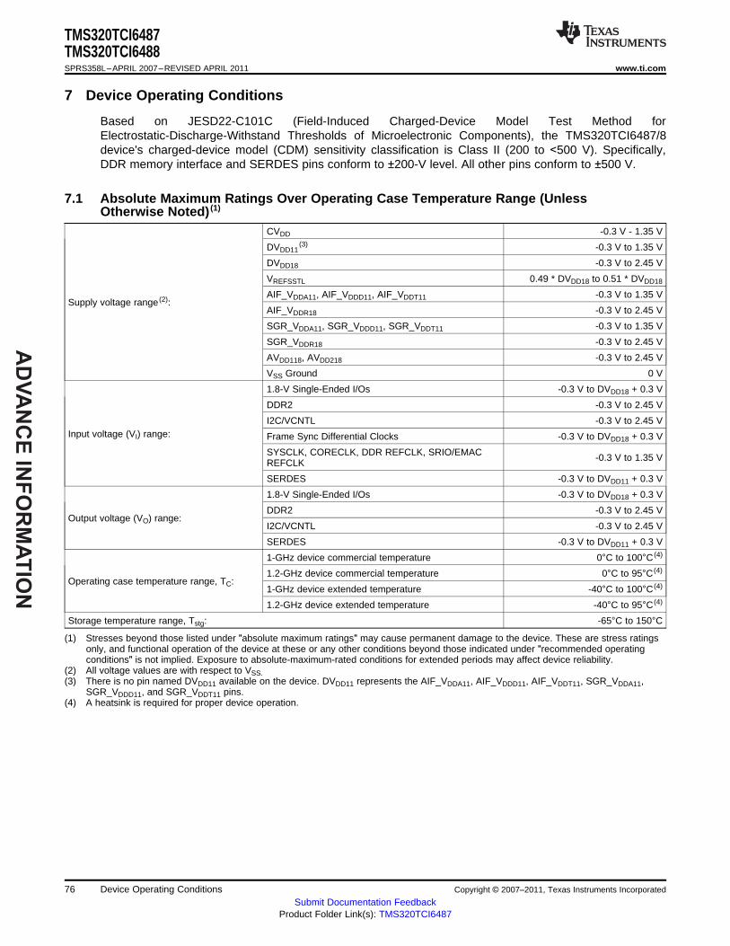
AD
VA
NC
E IN
FO
RM
AT
ION
TMS320TCI6487TMS320TCI6488SPRS358L–APRIL 2007–REVISED APRIL 2011 www.ti.com
7 Device Operating Conditions
Based on JESD22-C101C (Field-Induced Charged-Device Model Test Method forElectrostatic-Discharge-Withstand Thresholds of Microelectronic Components), the TMS320TCI6487/8device's charged-device model (CDM) sensitivity classification is Class II (200 to <500 V). Specifically,DDR memory interface and SERDES pins conform to ±200-V level. All other pins conform to ±500 V.
7.1 Absolute Maximum Ratings Over Operating Case Temperature Range (UnlessOtherwise Noted) (1)
CVDD -0.3 V - 1.35 V
DVDD11(3) -0.3 V to 1.35 V
DVDD18 -0.3 V to 2.45 V
VREFSSTL 0.49 * DVDD18 to 0.51 * DVDD18
AIF_VDDA11, AIF_VDDD11, AIF_VDDT11 -0.3 V to 1.35 VSupply voltage range (2):
AIF_VDDR18 -0.3 V to 2.45 V
SGR_VDDA11, SGR_VDDD11, SGR_VDDT11 -0.3 V to 1.35 V
SGR_VDDR18 -0.3 V to 2.45 V
AVDD118, AVDD218 -0.3 V to 2.45 V
VSS Ground 0 V
1.8-V Single-Ended I/Os -0.3 V to DVDD18 + 0.3 V
DDR2 -0.3 V to 2.45 V
I2C/VCNTL -0.3 V to 2.45 VInput voltage (VI) range: Frame Sync Differential Clocks -0.3 V to DVDD18 + 0.3 V
SYSCLK, CORECLK, DDR REFCLK, SRIO/EMAC -0.3 V to 1.35 VREFCLK
SERDES -0.3 V to DVDD11 + 0.3 V
1.8-V Single-Ended I/Os -0.3 V to DVDD18 + 0.3 V
DDR2 -0.3 V to 2.45 VOutput voltage (VO) range:
I2C/VCNTL -0.3 V to 2.45 V
SERDES -0.3 V to DVDD11 + 0.3 V
1-GHz device commercial temperature 0°C to 100°C (4)
1.2-GHz device commercial temperature 0°C to 95°C (4)
Operating case temperature range, TC:1-GHz device extended temperature -40°C to 100°C (4)
1.2-GHz device extended temperature -40°C to 95°C (4)
Storage temperature range, Tstg: -65°C to 150°C
(1) Stresses beyond those listed under "absolute maximum ratings" may cause permanent damage to the device. These are stress ratingsonly, and functional operation of the device at these or any other conditions beyond those indicated under "recommended operatingconditions" is not implied. Exposure to absolute-maximum-rated conditions for extended periods may affect device reliability.
(2) All voltage values are with respect to VSS.(3) There is no pin named DVDD11 available on the device. DVDD11 represents the AIF_VDDA11, AIF_VDDD11, AIF_VDDT11, SGR_VDDA11,
SGR_VDDD11, and SGR_VDDT11 pins.(4) A heatsink is required for proper device operation.
76 Device Operating Conditions Copyright © 2007–2011, Texas Instruments Incorporated
Submit Documentation FeedbackProduct Folder Link(s): TMS320TCI6487
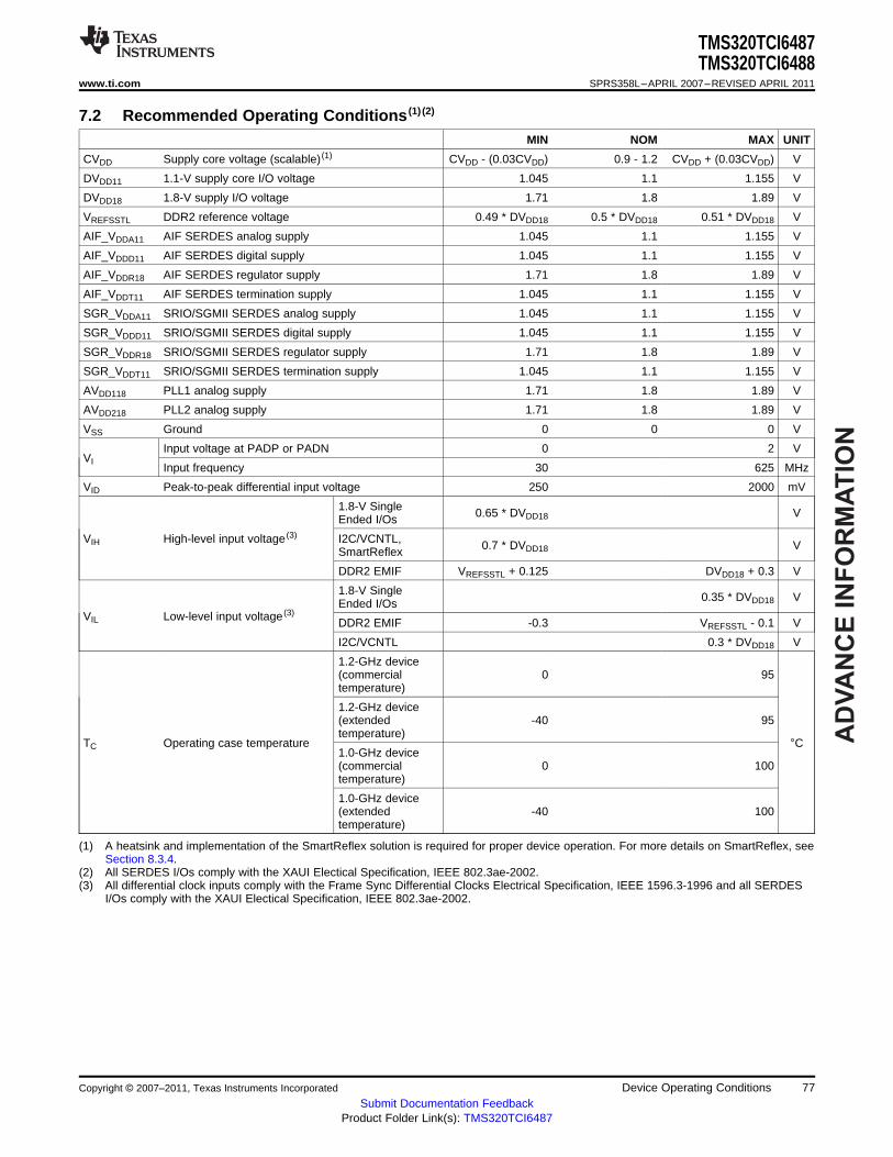
AD
VA
NC
E I
NF
OR
MA
TIO
N
TMS320TCI6487TMS320TCI6488
www.ti.com SPRS358L–APRIL 2007–REVISED APRIL 2011
7.2 Recommended Operating Conditions (1) (2)
MIN NOM MAX UNIT
CVDD Supply core voltage (scalable) (1) CVDD - (0.03CVDD) 0.9 - 1.2 CVDD + (0.03CVDD) V
DVDD11 1.1-V supply core I/O voltage 1.045 1.1 1.155 V
DVDD18 1.8-V supply I/O voltage 1.71 1.8 1.89 V
VREFSSTL DDR2 reference voltage 0.49 * DVDD18 0.5 * DVDD18 0.51 * DVDD18 V
AIF_VDDA11 AIF SERDES analog supply 1.045 1.1 1.155 V
AIF_VDDD11 AIF SERDES digital supply 1.045 1.1 1.155 V
AIF_VDDR18 AIF SERDES regulator supply 1.71 1.8 1.89 V
AIF_VDDT11 AIF SERDES termination supply 1.045 1.1 1.155 V
SGR_VDDA11 SRIO/SGMII SERDES analog supply 1.045 1.1 1.155 V
SGR_VDDD11 SRIO/SGMII SERDES digital supply 1.045 1.1 1.155 V
SGR_VDDR18 SRIO/SGMII SERDES regulator supply 1.71 1.8 1.89 V
SGR_VDDT11 SRIO/SGMII SERDES termination supply 1.045 1.1 1.155 V
AVDD118 PLL1 analog supply 1.71 1.8 1.89 V
AVDD218 PLL2 analog supply 1.71 1.8 1.89 V
VSS Ground 0 0 0 V
Input voltage at PADP or PADN 0 2 VVI
Input frequency 30 625 MHz
VID Peak-to-peak differential input voltage 250 2000 mV
1.8-V Single 0.65 * DVDD18 VEnded I/Os
VIH High-level input voltage (3) I2C/VCNTL, 0.7 * DVDD18 VSmartReflex
DDR2 EMIF VREFSSTL + 0.125 DVDD18 + 0.3 V
1.8-V Single 0.35 * DVDD18 VEnded I/OsVIL Low-level input voltage (3)
DDR2 EMIF -0.3 VREFSSTL - 0.1 V
I2C/VCNTL 0.3 * DVDD18 V
1.2-GHz device(commercial 0 95temperature)
1.2-GHz device(extended -40 95temperature)
TC Operating case temperature °C1.0-GHz device(commercial 0 100temperature)
1.0-GHz device(extended -40 100temperature)
(1) A heatsink and implementation of the SmartReflex solution is required for proper device operation. For more details on SmartReflex, seeSection 8.3.4.
(2) All SERDES I/Os comply with the XAUI Electical Specification, IEEE 802.3ae-2002.(3) All differential clock inputs comply with the Frame Sync Differential Clocks Electrical Specification, IEEE 1596.3-1996 and all SERDES
I/Os comply with the XAUI Electical Specification, IEEE 802.3ae-2002.
Copyright © 2007–2011, Texas Instruments Incorporated Device Operating Conditions 77Submit Documentation Feedback
Product Folder Link(s): TMS320TCI6487

AD
VA
NC
E IN
FO
RM
AT
ION
TMS320TCI6487TMS320TCI6488SPRS358L–APRIL 2007–REVISED APRIL 2011 www.ti.com
7.3 Electrical Characteristics Over Recommended Ranges of Supply Voltage andOperating Case Temperature (Unless Otherwise Noted)
PARAMETER TEST CONDITIONS (1) MIN TYP MAX UNIT
1.8-V Single Ended IO = IOH DVDD18 - 0.45I/OsHigh-levelVOH Voutput voltage DDR2 1.4
I2C/VCNTL 0.1 * DVdd18
1.8-V Single Ended IO = IOL 0.45I/OsLow-level outputVOL Vvoltage DDR2 0.4
I2C/VCNTL IO = 3 mA, pulled up to 1.8 V 0.4
No IPD/IPU -5 51.8-V Single Ended Internal pullup -169 -100 -47 μAI/OsInput currentII
(2)Internal pulldown 49 100 160[DC]0.1 * DVDD18 V < VI < 0.9 *I2C/VCNTL -20 20 μADVDD18 V
EMU[18:00], -8GPIO[15:0], TIMO[1:0]
SYSCLKOUT, TDO,CLKR0, CLKX0, DX0,FSR0, FSX0, CLKR1, -6High-levelCLKX1, DX1, FSR1,IOH output current mAFSX1[DC]RESETSTAT,SMFRAMECLK, MDIO, -4MDCLK
DDR2 4
EMU[18:00], 8GPIO[15:0], TIM[1:0]
SYSCLKOUT, TDO,CLKR0, CLKX0, DX0,FSR0, FSX0, CLKR1, 6
Low-level output CLKX1, DX1, FSR1,IOL mAcurrent [DC] FSX1
RESETSTAT,SMFRAMECLK, MDIO, 4MDCLK
DDR2 -4
Off-state output 1.8-V Single EndedIOZ(3) -20 20 μAcurrent [DC] I/Os
(1) For test conditions shown as MIN, MAX, or TYP, use the appropriate value specified in the recommended operating conditions table.(2) II applies to input-only pins and bi-directional pins. For input-only pins, II indicates the input leakage current. For bi-directional pins, II
includes input leakage current and off-state (hi-Z) output leakage current.(3) IOZ applies to output-only pins, indicating off-state (hi-Z) output leakage current.
78 Peripheral Information and Electrical Specifications Copyright © 2007–2011, Texas Instruments Incorporated
Submit Documentation FeedbackProduct Folder Link(s): TMS320TCI6487
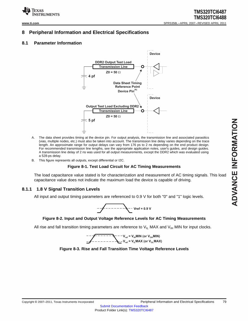
AD
VA
NC
E I
NF
OR
MA
TIO
N
Transmission Line
DDR2 Output Test Load
Z0 = 50 W
Data Sheet TimingReference Point
Device Pin(A)
Device
4 pf
Transmission Line
Output Test Load Excluding DDR2
Z0 = 50 W
Device
5 pf
Vref = 0.9 V
V = V MIN (or V MIN)ref IH OH
V = V MAX (or V MAX)ref IL OL
TMS320TCI6487TMS320TCI6488
www.ti.com SPRS358L–APRIL 2007–REVISED APRIL 2011
8 Peripheral Information and Electrical Specifications
8.1 Parameter Information
A. The data sheet provides timing at the device pin. For output analysis, the transmission line and associated parasitics(vias, multiple nodes, etc.) must also be taken into account. The transmission line delay varies depending on the tracelength. An approximate range for output delays can vary from 176 ps to 2 ns depending on the end product design.For recommended transmission line lengths, see the appropriate application notes, user's guides, and design guides.A transmission line delay of 2 ns was used for all output measurements, except the DDR2 which was evaluated usinga 528-ps delay.
B. This figure represents all outputs, except differential or I2C.
Figure 8-1. Test Load Circuit for AC Timing Measurements
The load capacitance value stated is for characterization and measurement of AC timing signals. This loadcapacitance value does not indicate the maximum load the device is capable of driving.
8.1.1 1.8 V Signal Transition Levels
All input and output timing parameters are referenced to 0.9 V for both "0" and "1" logic levels.
Figure 8-2. Input and Output Voltage Reference Levels for AC Timing Measurements
All rise and fall transition timing parameters are reference to VIL MAX and VIH MIN for input clocks.
Figure 8-3. Rise and Fall Transition Time Voltage Reference Levels
Copyright © 2007–2011, Texas Instruments Incorporated Peripheral Information and Electrical Specifications 79Submit Documentation Feedback
Product Folder Link(s): TMS320TCI6487

AD
VA
NC
E IN
FO
RM
AT
ION
DVDD18
VREFSSTL
CVDD11
DVDD11
POR
3
4
TMS320TCI6487TMS320TCI6488SPRS358L–APRIL 2007–REVISED APRIL 2011 www.ti.com
8.2 Recommended Clock and Control Signal Transition Behavior
All clocks and control signals must transition between VIH and VIL (or between VIL and VIH) in a monotonicmanner.
8.3 Power Supplies
8.3.1 Power-Supply Sequencing
Power supply sequencing must be followed as seen in Figure 8-4.
Table 8-1. Timing Requirements for Power Supply Ramping(see Figure 8-4)
NO. PARAMETERS MIN MAX UNIT
3 tsu(DVDD18-DVDD11) Setup Time, DVDD18 and VREFSSTL supply stable before 0.5 200 msDVDD11 and CVDD11 supplies stable (1)
4 th(DVDD11-POR) Hold time, POR low after CVDD11 and DVDD11 supplies stable (1) 100 μs
(1) Stable means that the voltage is valid as per Section 7.2, Recommended Operating Conditions.
Figure 8-4. Power-Supply Timing
For more information on power-supply sequencing, see the TMS320TCI6487/88 Hardware Design Guideapplication report (literature number SPRAAG5)
8.3.2 Power-Supply Decoupling
In order to properly decouple the supply planes from system noise, place as many capacitors (caps) aspossible close to the DSP. These caps need to be close to the DSP, no more than 1.25 cm maximumdistance to be effective. Physically smaller caps are better, such as 0402, but need to be evaluated from ayield/manufacturing point-of-view. Parasitic inductance limits the effectiveness of the decouplingcapacitors, therefore physically smaller capacitors should be used while maintaining the largest availablecapacitance value. As with the selection of any component, verification of capacitor availability over theproduct's production lifetime should be considered.
8.3.3 Power-Down Operation
One of the power goals for the TCI6487/8 device is to reduce power dissipation due to unusedperipherals. There are different ways to power down peripherals on the TCI6487/8 device.
80 Peripheral Information and Electrical Specifications Copyright © 2007–2011, Texas Instruments Incorporated
Submit Documentation FeedbackProduct Folder Link(s): TMS320TCI6487

AD
VA
NC
E I
NF
OR
MA
TIO
N
TMS320TCI6487TMS320TCI6488
www.ti.com SPRS358L–APRIL 2007–REVISED APRIL 2011
Some peripherals can be statically powered down at device reset through the device configuration pins(see Section 3.1, Device Configuration at Device Reset). Once in a static power-down state, the peripheralis held in reset and its clock is turned off. Peripherals cannot be enabled once they are in a staticpower-down state. To take a peripheral out of the static power-down state, a device reset must beexecuted with a different configuration pin setting.
After device reset, all peripherals on the TCI6487/8 device are in a disabled state and must be enabled bysoftware before being used. It is possible to enable only the peripherals needed by the application whilekeeping the rest disabled. Note that peripherals in a disabled state are held in reset with their clocksgated. For more information on how to enable peripherals, see Section 3.2, Peripheral Selection AfterDevice Reset.
Peripherals used for booting, like I2C, are automatically enabled after device reset. It is possible to disableperipherals used for booting after the boot process is complete. This, too, results in gating of the clock(s)to the powered-down peripheral. Once a peripheral is powered-down, it must remain powered down untilthe next device reset.
The C64x+ Megamodule also allows for software-driven power-down management for all of the C64x+Megamodule components through its Power-Down Controller (PDC). The CPU can power-down part orthe entire C64x+ Megamodule through the power-down controller based on its own execution thread or inresponse to an external stimulus from a host or global controller. More information on the power-downfeatures of the C64x+ Megamodule can be found in the TMS320C64x+ Megamodule Reference Guide(literature number SPRU871).
Table 8-2 lists the Power/Sleep Controller (PSC) registers.
Table 8-2. Power/Sleep Controller Registers
HEX ADDRESS ACRONYM REGISTER NAME
02AC 0000 PID Peripheral Revision and Class Information
02AC 0120 PTCMD Power Domain Transition Command Register
02AC 0128 PTSTAT Power Domain Transition Status Register
02AC 0200 PDSTAT Power Domain Status Register
02AC 0300 PDCTL0 Power Domain Control Register 0 (AlwaysOn)
02AC 0304 PDCTL1 Power Domain Control Register 1 (Antenna Interface)
02AC 0308 PDCTL2 Power Domain Control Register 2 (Serial RapidIO)
02AC 030C PDCTL3 Power Domain Control Register 3 (RAC) (TCI6488 only)
02AC 0310 PDCTL4 Power Domain Control Register 4 (TCP)
02AC 0314 PDCTL5 Power Domain Control Register 5 (VCP)
02AC 0800 MDSTAT0
02AC 0804
02AC 0808
02AC 080C MDSTAT3 Module Status Register 3 (C64x+ Core 0)
02AC 0810 MDSTAT4 Module Status Register 4 (C64x+ Core 1)
02AC 0814 MDSTAT5 Module Status Register 5 (C64x+ Core 2)
02AC 0818 MDSTAT6 Module Status Register 6 (Antenna Interface)
02AC 081C MDSTAT7 Module Status Register 7 (Serial RapidIO)
02AC 0820 MDSTAT8 Module Status Register 8 (RAC) (TCI6488 only)
02AC 0824 MDSTAT9 Module Status Register 9 (TCP)
02AC 0828 MDSTAT10 Module Status Register 10 (VCP)
02AC 082C MDSTAT11 Module Status Register 11 (Never Gated)
02AC 0A00 MDCTL0 Module Control Register 0 (C64x+ Core 0 RSAs)
02AC 0A04 MDCTL1 Module Control Register 1 (C64x+ Core 1 RSAs)
02AC 0A08 MDCTL2 Module Control Register 2 (C64x+ Core 2 RSAs)
Copyright © 2007–2011, Texas Instruments Incorporated Peripheral Information and Electrical Specifications 81Submit Documentation Feedback
Product Folder Link(s): TMS320TCI6487
AD
VA
NC
E IN
FO
RM
AT
ION
TMS320TCI6487TMS320TCI6488SPRS358L–APRIL 2007–REVISED APRIL 2011 www.ti.com
Table 8-2. Power/Sleep Controller Registers (continued)
HEX ADDRESS ACRONYM REGISTER NAME
02AC 0A0C MDCTL3 Module Control Register 3 (C64x+ Core 0)
02AC 0A10 MDCTL4 Module Control Register 4 (C64x+ Core 1)
02AC 0A14 MDCTL5 Module Control Register 5 (C64x+ Core 2)
02AC 0A18 MDCTL6 Module Control Register 6 (Antenna Interface)
02AC 0A1C MDCTL7 Module Control Register 7 (Serial RapidIO)
02AC 0A20 MDCTL8 Module Control Register 8 (RAC) (TCI6488 only)
02AC 0A24 MDCTL9 Module Control Register 9 (TCP)
02AC 0A28 MDCTL10 Module Control Register 10 (VCP)
02AC 0A2C MDCTL11 Module Control Register 11 (Never Gated)
8.3.4 SmartReflex
Increasing the device complexity increases its power consumption and with the smaller transistorstructures responsible for higher achievable clock rates and increased performance, comes an inevitablepenalty, increasing the leakage currents. Leakage currents are present in any active circuit, independentlyof clock rates and usage scenarios. This static power consumption is mainly determined by transistor typeand process technology. Higher clock rates also increase dynamic power, the power used whentransistors switch. The dynamic power depends mainly on a specific usage scenario, clock rates, and I/Oactivity.
Texas Instruments' SmartReflex™ technology is used to decrease both static and dynamic powerconsumption while maintaining the device performance. SmartReflex in the TCI6487/8 device is a featurethat allows the core voltage to be optimized based on the process corner of the device. This requires avoltage regulator for each TCI6487/8 device.
To guarantee maximizing performance and minimizing power consumption of the device, SmartReflex isrequired to be implemented whenever the TCI6487/8 device is used.
The voltage selection is done using 4 VCNTL pins which are used to select the output voltage of the corevoltage regulator. For complete information on SmartReflex, see the TMS320TCI6487/88 HardwareDesign Guide application report (literature number SPRAAG5).
82 Peripheral Information and Electrical Specifications Copyright © 2007–2011, Texas Instruments Incorporated
Submit Documentation FeedbackProduct Folder Link(s): TMS320TCI6487

AD
VA
NC
E I
NF
OR
MA
TIO
N
TMS320TCI6487TMS320TCI6488
www.ti.com SPRS358L–APRIL 2007–REVISED APRIL 2011
8.4 Peripheral IDs (PIDs)
The peripheral ID is a unique ID for each peripheral module. It represents the module version details.Table 8-3 shows the PIDs for each peripheral module.
Table 8-3. TCI6487/8 Modules Peripheral IDs
PIDMEMORY MAPPEDSR NO. MODULE ADDRESS PG1.2 PG1.3 PG2.0
1 EDMA TC0 0x02A20000 0x40003300 0x40003300 0x40003300
2 EDMA TC1 0x02A28000 0x40003300 0x40003300 0x40003300
3 EDMA TC2 0x02A30000 0x40003300 0x40003300 0x40003300
4 EDMA TC3 0x02A38000 0x40003300 0x40003300 0x40003300
5 EDMA TC4 0x02A40000 0x40003300 0x40003300 0x40003300
6 EDMA TC5 0x02A48000 0x40003300 0x40003300 0x40003300
7 EDMA CC 0x02A00000 0x40015300 0x40015340 0x40015340
8 DDR2 0x70000000 0x0031031b 0x0031031b 0x0031031b
9 McBSP0 0x028C0058 0x00020103 0x00020103 0x00020103
10 McBSP1 0x028D0058 0x00020103 0x00020103 0x00020103
11 I2C PID1 0x02B04034 0x00000106 0x00000106 0x00000106
12 I2C PID2 0x02B04038 0x00000005 0x00000005 0x00000005
13 Timer64_0 0x02910000 0x00010701 0x00010701 0x00010701
14 Timer64_1 0x02920000 0x00010701 0x00010701 0x00010701
15 Timer64_2 0x02930000 0x00010701 0x00010701 0x00010701
16 Timer64_3 0x02940000 0x00010701 0x00010701 0x00010701
17 Timer64_4 0x02950000 0x00010701 0x00010701 0x00010701
18 Timer64_5 0x02960000 0x00010701 0x00010701 0x00010701
19 PLL CTRL 0x029A0000 0x0001080d 0x0001080d 0x0001080d
20 PSC 0x02AC0000 0x44821105 0x44821105 0x44821105
21 GPIO 0x02B00000 0x44830105 0x44830105 0x44830105
22 SRIO 0x02D00000 0x44A43102 0x44A43102 0x44A43102
23 AIF 0x02BC0000 0x4800200C 0x4800200C 0x4800200C
24 FSYNC 0x02800000 0x48010900 0x48010900 0x48010900
25 RAC (TCI6488 only) 0x02F00000 0x48030000 0x48030000 0x48030801
26 TCP3 0x02BA0000 0x00021105 0x00021105 0x00021105
27 EMAC TX 0x02C80000 0x000C0A0B 0x000C0A0B 0x000C0A0B
28 EMAC RX 0x02C80010 0x000C0A0B 0x000C0A0B 0x000C0A0B
29 MDIO 0X02C81800 0x00070104 0x00070104 0x00070104
30 SGMII 0x02C40000 0x002c0100 0x002C0100 0x002C0100
31 EMAC Control Module 0x02C81000 0x002d0102 0x002d0102 0x002d0102
32 SEM 0x02B40000 0x48020100 0x48020100 0x48020100
33 VCP 0x02B80000 0x00011107 0x00011107 0x00011107
Copyright © 2007–2011, Texas Instruments Incorporated Peripheral Information and Electrical Specifications 83Submit Documentation Feedback
Product Folder Link(s): TMS320TCI6487

AD
VA
NC
E IN
FO
RM
AT
ION
TMS320TCI6487TMS320TCI6488SPRS358L–APRIL 2007–REVISED APRIL 2011 www.ti.com
8.5 Enhanced Direct Memory Access (EDMA3) Controller
The primary purpose of the EDMA3 is to service user-programmed data transfers between twomemory-mapped slave endpoints on the device. The EDMA3 services software-driven paging transfers(e.g., data movement between external memory and internal memory), performs sorting or subframeextraction of various data structures, services event driven peripherals such as a McBSP port, andoffloads data transfers from the device CPU.
The EDMA3 includes the following features:• Fully orthogonal transfer description
– 3 transfer dimensions: array (multiple bytes), frame (multiple arrays), and block (multiple frames)– Single event can trigger transfer of array, frame, or entire block– Independent indexes on source and destination
• Flexible transfer definition:– Increment or FIFO transfer addressing modes– Linking mechanism allows for ping-pong buffering, circular buffering, and repetitive/continuous
transfers, all with no CPU intervention– Chaining allows multiple transfers to execute with one event
• 256 PaRAM entries– Used to define transfer context for channels– Each PaRAM entry can be used as a DMA entry, QDMA entry, or link entry
• 64 DMA channels– Manually triggered (CPU writes to channel controller register), external event triggered, and chain
triggered (completion of one transfer triggers another)• 8 Quick DMA (QDMA) channels
– Used for software-driven transfers– Triggered upon writing to a single PaRAM set entry
• 6 transfer controllers and 6 event queues with programmable system-level priority• Interrupt generation for transfer completion and error conditions• Debug visibility
– Queue watermarking/threshold allows detection of maximum usage of event queues– Error and status recording to facilitate debug
Each of the transfer controllers has a direct connection to the switched central resource (SCR). Table 4-1lists the peripherals that can be accessed by the transfer controllers.
84 Peripheral Information and Electrical Specifications Copyright © 2007–2011, Texas Instruments Incorporated
Submit Documentation FeedbackProduct Folder Link(s): TMS320TCI6487
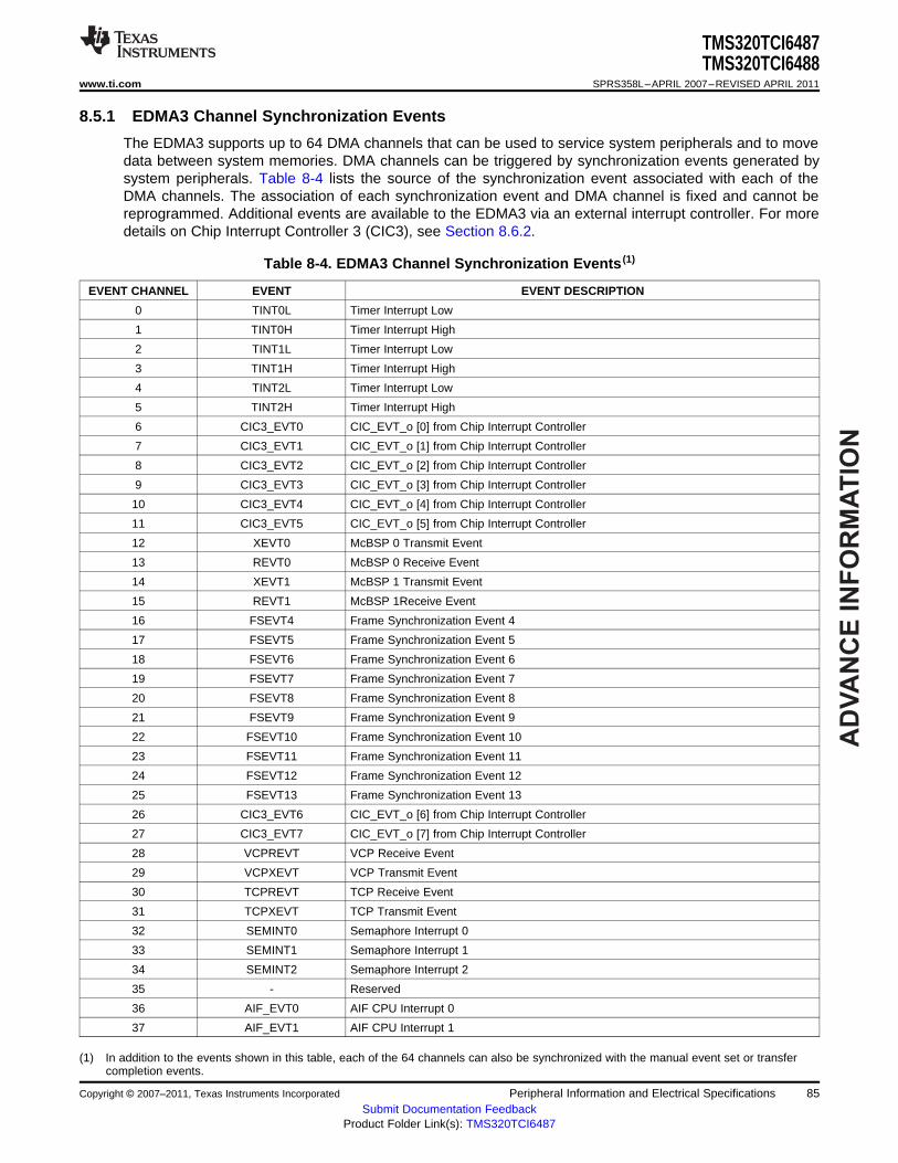
AD
VA
NC
E I
NF
OR
MA
TIO
N
TMS320TCI6487TMS320TCI6488
www.ti.com SPRS358L–APRIL 2007–REVISED APRIL 2011
8.5.1 EDMA3 Channel Synchronization Events
The EDMA3 supports up to 64 DMA channels that can be used to service system peripherals and to movedata between system memories. DMA channels can be triggered by synchronization events generated bysystem peripherals. Table 8-4 lists the source of the synchronization event associated with each of theDMA channels. The association of each synchronization event and DMA channel is fixed and cannot bereprogrammed. Additional events are available to the EDMA3 via an external interrupt controller. For moredetails on Chip Interrupt Controller 3 (CIC3), see Section 8.6.2.
Table 8-4. EDMA3 Channel Synchronization Events (1)
EVENT CHANNEL EVENT EVENT DESCRIPTION
0 TINT0L Timer Interrupt Low
1 TINT0H Timer Interrupt High
2 TINT1L Timer Interrupt Low
3 TINT1H Timer Interrupt High
4 TINT2L Timer Interrupt Low
5 TINT2H Timer Interrupt High
6 CIC3_EVT0 CIC_EVT_o [0] from Chip Interrupt Controller
7 CIC3_EVT1 CIC_EVT_o [1] from Chip Interrupt Controller
8 CIC3_EVT2 CIC_EVT_o [2] from Chip Interrupt Controller
9 CIC3_EVT3 CIC_EVT_o [3] from Chip Interrupt Controller
10 CIC3_EVT4 CIC_EVT_o [4] from Chip Interrupt Controller
11 CIC3_EVT5 CIC_EVT_o [5] from Chip Interrupt Controller
12 XEVT0 McBSP 0 Transmit Event
13 REVT0 McBSP 0 Receive Event
14 XEVT1 McBSP 1 Transmit Event
15 REVT1 McBSP 1Receive Event
16 FSEVT4 Frame Synchronization Event 4
17 FSEVT5 Frame Synchronization Event 5
18 FSEVT6 Frame Synchronization Event 6
19 FSEVT7 Frame Synchronization Event 7
20 FSEVT8 Frame Synchronization Event 8
21 FSEVT9 Frame Synchronization Event 9
22 FSEVT10 Frame Synchronization Event 10
23 FSEVT11 Frame Synchronization Event 11
24 FSEVT12 Frame Synchronization Event 12
25 FSEVT13 Frame Synchronization Event 13
26 CIC3_EVT6 CIC_EVT_o [6] from Chip Interrupt Controller
27 CIC3_EVT7 CIC_EVT_o [7] from Chip Interrupt Controller
28 VCPREVT VCP Receive Event
29 VCPXEVT VCP Transmit Event
30 TCPREVT TCP Receive Event
31 TCPXEVT TCP Transmit Event
32 SEMINT0 Semaphore Interrupt 0
33 SEMINT1 Semaphore Interrupt 1
34 SEMINT2 Semaphore Interrupt 2
35 - Reserved
36 AIF_EVT0 AIF CPU Interrupt 0
37 AIF_EVT1 AIF CPU Interrupt 1
(1) In addition to the events shown in this table, each of the 64 channels can also be synchronized with the manual event set or transfercompletion events.
Copyright © 2007–2011, Texas Instruments Incorporated Peripheral Information and Electrical Specifications 85Submit Documentation Feedback
Product Folder Link(s): TMS320TCI6487
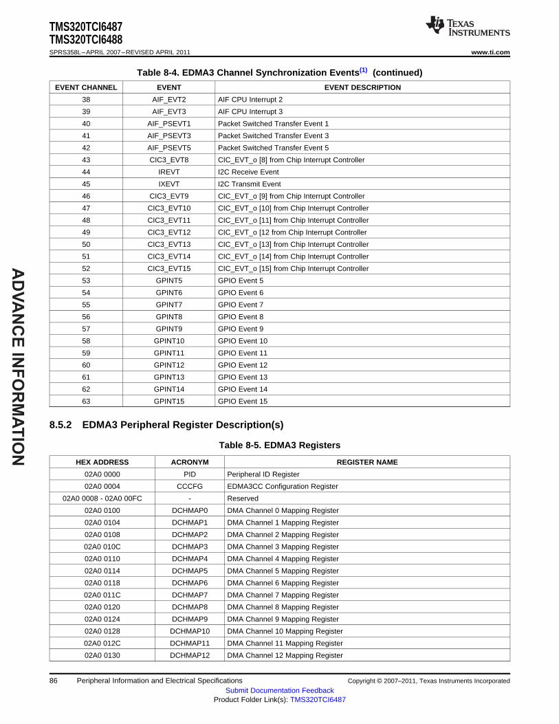
AD
VA
NC
E IN
FO
RM
AT
ION
TMS320TCI6487TMS320TCI6488SPRS358L–APRIL 2007–REVISED APRIL 2011 www.ti.com
Table 8-4. EDMA3 Channel Synchronization Events(1) (continued)
EVENT CHANNEL EVENT EVENT DESCRIPTION
38 AIF_EVT2 AIF CPU Interrupt 2
39 AIF_EVT3 AIF CPU Interrupt 3
40 AIF_PSEVT1 Packet Switched Transfer Event 1
41 AIF_PSEVT3 Packet Switched Transfer Event 3
42 AIF_PSEVT5 Packet Switched Transfer Event 5
43 CIC3_EVT8 CIC_EVT_o [8] from Chip Interrupt Controller
44 IREVT I2C Receive Event
45 IXEVT I2C Transmit Event
46 CIC3_EVT9 CIC_EVT_o [9] from Chip Interrupt Controller
47 CIC3_EVT10 CIC_EVT_o [10] from Chip Interrupt Controller
48 CIC3_EVT11 CIC_EVT_o [11] from Chip Interrupt Controller
49 CIC3_EVT12 CIC_EVT_o [12 from Chip Interrupt Controller
50 CIC3_EVT13 CIC_EVT_o [13] from Chip Interrupt Controller
51 CIC3_EVT14 CIC_EVT_o [14] from Chip Interrupt Controller
52 CIC3_EVT15 CIC_EVT_o [15] from Chip Interrupt Controller
53 GPINT5 GPIO Event 5
54 GPINT6 GPIO Event 6
55 GPINT7 GPIO Event 7
56 GPINT8 GPIO Event 8
57 GPINT9 GPIO Event 9
58 GPINT10 GPIO Event 10
59 GPINT11 GPIO Event 11
60 GPINT12 GPIO Event 12
61 GPINT13 GPIO Event 13
62 GPINT14 GPIO Event 14
63 GPINT15 GPIO Event 15
8.5.2 EDMA3 Peripheral Register Description(s)
Table 8-5. EDMA3 Registers
HEX ADDRESS ACRONYM REGISTER NAME
02A0 0000 PID Peripheral ID Register
02A0 0004 CCCFG EDMA3CC Configuration Register
02A0 0008 - 02A0 00FC - Reserved
02A0 0100 DCHMAP0 DMA Channel 0 Mapping Register
02A0 0104 DCHMAP1 DMA Channel 1 Mapping Register
02A0 0108 DCHMAP2 DMA Channel 2 Mapping Register
02A0 010C DCHMAP3 DMA Channel 3 Mapping Register
02A0 0110 DCHMAP4 DMA Channel 4 Mapping Register
02A0 0114 DCHMAP5 DMA Channel 5 Mapping Register
02A0 0118 DCHMAP6 DMA Channel 6 Mapping Register
02A0 011C DCHMAP7 DMA Channel 7 Mapping Register
02A0 0120 DCHMAP8 DMA Channel 8 Mapping Register
02A0 0124 DCHMAP9 DMA Channel 9 Mapping Register
02A0 0128 DCHMAP10 DMA Channel 10 Mapping Register
02A0 012C DCHMAP11 DMA Channel 11 Mapping Register
02A0 0130 DCHMAP12 DMA Channel 12 Mapping Register
86 Peripheral Information and Electrical Specifications Copyright © 2007–2011, Texas Instruments Incorporated
Submit Documentation FeedbackProduct Folder Link(s): TMS320TCI6487
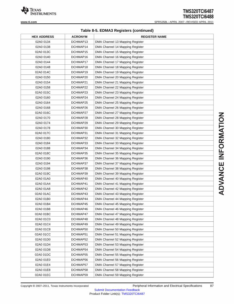
AD
VA
NC
E I
NF
OR
MA
TIO
N
TMS320TCI6487TMS320TCI6488
www.ti.com SPRS358L–APRIL 2007–REVISED APRIL 2011
Table 8-5. EDMA3 Registers (continued)
HEX ADDRESS ACRONYM REGISTER NAME
02A0 0134 DCHMAP13 DMA Channel 13 Mapping Register
02A0 0138 DCHMAP14 DMA Channel 14 Mapping Register
02A0 013C DCHMAP15 DMA Channel 15 Mapping Register
02A0 0140 DCHMAP16 DMA Channel 16 Mapping Register
02A0 0144 DCHMAP17 DMA Channel 17 Mapping Register
02A0 0148 DCHMAP18 DMA Channel 18 Mapping Register
02A0 014C DCHMAP19 DMA Channel 19 Mapping Register
02A0 0150 DCHMAP20 DMA Channel 20 Mapping Register
02A0 0154 DCHMAP21 DMA Channel 21 Mapping Register
02A0 0158 DCHMAP22 DMA Channel 22 Mapping Register
02A0 015C DCHMAP23 DMA Channel 23 Mapping Register
02A0 0160 DCHMAP24 DMA Channel 24 Mapping Register
02A0 0164 DCHMAP25 DMA Channel 25 Mapping Register
02A0 0168 DCHMAP26 DMA Channel 26 Mapping Register
02A0 016C DCHMAP27 DMA Channel 27 Mapping Register
02A0 0170 DCHMAP28 DMA Channel 28 Mapping Register
02A0 0174 DCHMAP29 DMA Channel 29 Mapping Register
02A0 0178 DCHMAP30 DMA Channel 30 Mapping Register
02A0 017C DCHMAP31 DMA Channel 31 Mapping Register
02A0 0180 DCHMAP32 DMA Channel 32 Mapping Register
02A0 0184 DCHMAP33 DMA Channel 33 Mapping Register
02A0 0188 DCHMAP34 DMA Channel 34 Mapping Register
02A0 018C DCHMAP35 DMA Channel 35 Mapping Register
02A0 0190 DCHMAP36 DMA Channel 36 Mapping Register
02A0 0194 DCHMAP37 DMA Channel 37 Mapping Register
02A0 0198 DCHMAP38 DMA Channel 38 Mapping Register
02A0 019C DCHMAP39 DMA Channel 39 Mapping Register
02A0 01A0 DCHMAP40 DMA Channel 40 Mapping Register
02A0 01A4 DCHMAP41 DMA Channel 41 Mapping Register
02A0 01A8 DCHMAP42 DMA Channel 42 Mapping Register
02A0 01AC DCHMAP43 DMA Channel 43 Mapping Register
02A0 01B0 DCHMAP44 DMA Channel 44 Mapping Register
02A0 01B4 DCHMAP45 DMA Channel 45 Mapping Register
02A0 01B8 DCHMAP46 DMA Channel 46 Mapping Register
02A0 01BC DCHMAP47 DMA Channel 47 Mapping Register
02A0 01C0 DCHMAP48 DMA Channel 48 Mapping Register
02A0 01C4 DCHMAP49 DMA Channel 49 Mapping Register
02A0 01C8 DCHMAP50 DMA Channel 50 Mapping Register
02A0 01CC DCHMAP51 DMA Channel 51 Mapping Register
02A0 01D0 DCHMAP52 DMA Channel 52 Mapping Register
02A0 01D4 DCHMAP53 DMA Channel 53 Mapping Register
02A0 01D8 DCHMAP54 DMA Channel 54 Mapping Register
02A0 01DC DCHMAP55 DMA Channel 55 Mapping Register
02A0 01E0 DCHMAP56 DMA Channel 56 Mapping Register
02A0 01E4 DCHMAP57 DMA Channel 57 Mapping Register
02A0 01E8 DCHMAP58 DMA Channel 58 Mapping Register
02A0 01EC DCHMAP59 DMA Channel 59 Mapping Register
Copyright © 2007–2011, Texas Instruments Incorporated Peripheral Information and Electrical Specifications 87Submit Documentation Feedback
Product Folder Link(s): TMS320TCI6487

AD
VA
NC
E IN
FO
RM
AT
ION
TMS320TCI6487TMS320TCI6488SPRS358L–APRIL 2007–REVISED APRIL 2011 www.ti.com
Table 8-5. EDMA3 Registers (continued)
HEX ADDRESS ACRONYM REGISTER NAME
02A0 01F0 DCHMAP60 DMA Channel 60 Mapping Register
02A0 01F4 DCHMAP61 DMA Channel 61 Mapping Register
02A0 01F8 DCHMAP62 DMA Channel 62 Mapping Register
02A0 01FC DCHMAP63 DMA Channel 63 Mapping Register
02A0 0200 QCHMAP0 QDMA Channel 0 Mapping Register
02A0 0204 QCHMAP1 QDMA Channel 1 Mapping Register
02A0 0208 QCHMAP2 QDMA Channel 2 Mapping Register
02A0 020C QCHMAP3 QDMA Channel 3 Mapping Register
02A0 0210 QCHMAP4 QDMA Channel 4 Mapping Register
02A0 0214 QCHMAP5 QDMA Channel 5 Mapping Register
02A0 0218 QCHMAP6 QDMA Channel 6 Mapping Register
02A0 021C QCHMAP7 QDMA Channel 7 Mapping Register
02A0 0220 - 02A0 023C - Reserved
02A0 0240 DMAQNUM0 DMA Queue Number Register 0
02A0 0244 DMAQNUM1 DMA Queue Number Register 1
02A0 0248 DMAQNUM2 DMA Queue Number Register 2
02A0 024C DMAQNUM3 DMA Queue Number Register 3
02A0 0250 DMAQNUM4 DMA Queue Number Register 4
02A0 0254 DMAQNUM5 DMA Queue Number Register 5
02A0 0258 DMAQNUM6 DMA Queue Number Register 6
02A0 025C DMAQNUM7 DMA Queue Number Register 7
02A0 0260 QDMAQNUM QDMA Queue Number Register
02A0 0264 - 02A0 027C - Reserved
02A0 0280 QUETCMAP Queue to TC Mapping Register
02A0 0284 QUEPRI Queue Priority Register
02A0 0288 - 02A0 02FC - Reserved
02A0 0300 EMR Event Missed Register
02A0 0304 EMRH Event Missed Register High
02A0 0308 EMCR Event Missed Clear Register
02A0 030C EMCRH Event Missed Clear Register High
02A0 0310 QEMR QDMA Event Missed Register
02A0 0314 QEMCR QDMA Event Missed Clear Register
02A0 0318 CCERR EDMA3CC Error Register
02A0 031C CCERRCLR EDMA3CC Error Clear Register
02A0 0320 EEVAL Error Evaluate Register
02A0 0324 - 02A0 033C - Reserved
02A0 0340 DRAE0 DMA Region Access Enable Register for Region 0
02A0 0344 DRAEH0 DMA Region Access Enable Register High for Region 0
02A0 0348 DRAE1 DMA Region Access Enable Register for Region 1
02A0 034C DRAEH1 DMA Region Access Enable Register High for Region 1
02A0 0350 DRAE2 DMA Region Access Enable Register for Region 2
02A0 0354 DRAEH2 DMA Region Access Enable Register High for Region 2
02A0 0358 DRAE3 DMA Region Access Enable Register for Region 3
02A0 035C DRAEH3 DMA Region Access Enable Register High for Region 3
02A0 0360 DRAE4 DMA Region Access Enable Register for Region 4
02A0 0364 DRAEH4 DMA Region Access Enable Register High for Region 4
02A0 0368 DRAE5 DMA Region Access Enable Register for Region 5
88 Peripheral Information and Electrical Specifications Copyright © 2007–2011, Texas Instruments Incorporated
Submit Documentation FeedbackProduct Folder Link(s): TMS320TCI6487
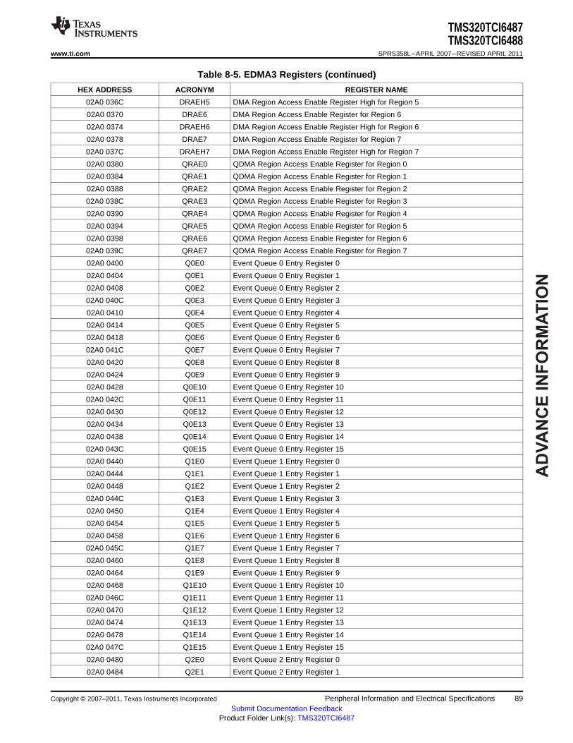
AD
VA
NC
E I
NF
OR
MA
TIO
N
TMS320TCI6487TMS320TCI6488
www.ti.com SPRS358L–APRIL 2007–REVISED APRIL 2011
Table 8-5. EDMA3 Registers (continued)
HEX ADDRESS ACRONYM REGISTER NAME
02A0 036C DRAEH5 DMA Region Access Enable Register High for Region 5
02A0 0370 DRAE6 DMA Region Access Enable Register for Region 6
02A0 0374 DRAEH6 DMA Region Access Enable Register High for Region 6
02A0 0378 DRAE7 DMA Region Access Enable Register for Region 7
02A0 037C DRAEH7 DMA Region Access Enable Register High for Region 7
02A0 0380 QRAE0 QDMA Region Access Enable Register for Region 0
02A0 0384 QRAE1 QDMA Region Access Enable Register for Region 1
02A0 0388 QRAE2 QDMA Region Access Enable Register for Region 2
02A0 038C QRAE3 QDMA Region Access Enable Register for Region 3
02A0 0390 QRAE4 QDMA Region Access Enable Register for Region 4
02A0 0394 QRAE5 QDMA Region Access Enable Register for Region 5
02A0 0398 QRAE6 QDMA Region Access Enable Register for Region 6
02A0 039C QRAE7 QDMA Region Access Enable Register for Region 7
02A0 0400 Q0E0 Event Queue 0 Entry Register 0
02A0 0404 Q0E1 Event Queue 0 Entry Register 1
02A0 0408 Q0E2 Event Queue 0 Entry Register 2
02A0 040C Q0E3 Event Queue 0 Entry Register 3
02A0 0410 Q0E4 Event Queue 0 Entry Register 4
02A0 0414 Q0E5 Event Queue 0 Entry Register 5
02A0 0418 Q0E6 Event Queue 0 Entry Register 6
02A0 041C Q0E7 Event Queue 0 Entry Register 7
02A0 0420 Q0E8 Event Queue 0 Entry Register 8
02A0 0424 Q0E9 Event Queue 0 Entry Register 9
02A0 0428 Q0E10 Event Queue 0 Entry Register 10
02A0 042C Q0E11 Event Queue 0 Entry Register 11
02A0 0430 Q0E12 Event Queue 0 Entry Register 12
02A0 0434 Q0E13 Event Queue 0 Entry Register 13
02A0 0438 Q0E14 Event Queue 0 Entry Register 14
02A0 043C Q0E15 Event Queue 0 Entry Register 15
02A0 0440 Q1E0 Event Queue 1 Entry Register 0
02A0 0444 Q1E1 Event Queue 1 Entry Register 1
02A0 0448 Q1E2 Event Queue 1 Entry Register 2
02A0 044C Q1E3 Event Queue 1 Entry Register 3
02A0 0450 Q1E4 Event Queue 1 Entry Register 4
02A0 0454 Q1E5 Event Queue 1 Entry Register 5
02A0 0458 Q1E6 Event Queue 1 Entry Register 6
02A0 045C Q1E7 Event Queue 1 Entry Register 7
02A0 0460 Q1E8 Event Queue 1 Entry Register 8
02A0 0464 Q1E9 Event Queue 1 Entry Register 9
02A0 0468 Q1E10 Event Queue 1 Entry Register 10
02A0 046C Q1E11 Event Queue 1 Entry Register 11
02A0 0470 Q1E12 Event Queue 1 Entry Register 12
02A0 0474 Q1E13 Event Queue 1 Entry Register 13
02A0 0478 Q1E14 Event Queue 1 Entry Register 14
02A0 047C Q1E15 Event Queue 1 Entry Register 15
02A0 0480 Q2E0 Event Queue 2 Entry Register 0
02A0 0484 Q2E1 Event Queue 2 Entry Register 1
Copyright © 2007–2011, Texas Instruments Incorporated Peripheral Information and Electrical Specifications 89Submit Documentation Feedback
Product Folder Link(s): TMS320TCI6487

AD
VA
NC
E IN
FO
RM
AT
ION
TMS320TCI6487TMS320TCI6488SPRS358L–APRIL 2007–REVISED APRIL 2011 www.ti.com
Table 8-5. EDMA3 Registers (continued)
HEX ADDRESS ACRONYM REGISTER NAME
02A0 0488 Q2E2 Event Queue 2 Entry Register 2
02A0 048C Q2E3 Event Queue 2 Entry Register 3
02A0 0490 Q2E4 Event Queue 2 Entry Register 4
02A0 0494 Q2E5 Event Queue 2 Entry Register 5
02A0 0498 Q2E6 Event Queue 2 Entry Register 6
02A0 049C Q2E7 Event Queue 2 Entry Register 7
02A0 04A0 Q2E8 Event Queue 2 Entry Register 8
02A0 04A4 Q2E9 Event Queue 2 Entry Register 9
02A0 04A8 Q2E10 Event Queue 2 Entry Register 10
02A0 04AC Q2E11 Event Queue 2 Entry Register 11
02A0 04B0 Q2E12 Event Queue 2 Entry Register 12
02A0 04B4 Q2E13 Event Queue 2 Entry Register 13
02A0 04B8 Q2E14 Event Queue 2 Entry Register 14
02A0 04BC Q2E15 Event Queue 2 Entry Register 15
02A0 04C0 Q3E0 Event Queue 3 Entry Register 0
02A0 04C4 Q3E1 Event Queue 3 Entry Register 1
02A0 04C8 Q3E2 Event Queue 3 Entry Register 2
02A0 04CC Q3E3 Event Queue 3 Entry Register 3
02A0 04D0 Q3E4 Event Queue 3 Entry Register 4
02A0 04D4 Q3E5 Event Queue 3 Entry Register 5
02A0 04D8 Q3E6 Event Queue 3 Entry Register 6
02A0 04DC Q3E7 Event Queue 3 Entry Register 7
02A0 04E0 Q3E8 Event Queue 3 Entry Register 8
02A0 04E4 Q3E9 Event Queue 3 Entry Register 9
02A0 04E8 Q3E10 Event Queue 3 Entry Register 10
02A0 04EC Q3E11 Event Queue 3 Entry Register 11
02A0 04F0 Q3E12 Event Queue 3 Entry Register 12
02A0 04F4 Q3E13 Event Queue 3 Entry Register 13
02A0 04F8 Q3E14 Event Queue 3 Entry Register 14
02A0 04FC Q3E15 Event Queue 3 Entry Register 15
02A0 0500 Q4E0 Event Queue 4 Entry Register 0
02A0 0504 Q4E1 Event Queue 4 Entry Register 1
02A0 0508 Q4E2 Event Queue 4 Entry Register 2
02A0 050C Q4E3 Event Queue 4 Entry Register 3
02A0 0510 Q4E4 Event Queue 4 Entry Register 4
02A0 0514 Q4E5 Event Queue 4 Entry Register 5
02A0 0518 Q4E6 Event Queue 4 Entry Register 6
02A0 051C Q4E7 Event Queue 4 Entry Register 7
02A0 0520 Q4E8 Event Queue 4 Entry Register 8
02A0 0524 Q4E9 Event Queue 4 Entry Register 9
02A0 0528 Q4E10 Event Queue 4 Entry Register 10
02A0 052C Q4E11 Event Queue 4 Entry Register 11
02A0 0530 Q4E12 Event Queue 4 Entry Register 12
02A0 0534 Q4E13 Event Queue 4 Entry Register 13
02A0 0538 Q4E14 Event Queue 4 Entry Register 14
02A0 053C Q4E15 Event Queue 4 Entry Register 15
02A0 0540 Q5E0 Event Queue 5 Entry Register 0
90 Peripheral Information and Electrical Specifications Copyright © 2007–2011, Texas Instruments Incorporated
Submit Documentation FeedbackProduct Folder Link(s): TMS320TCI6487
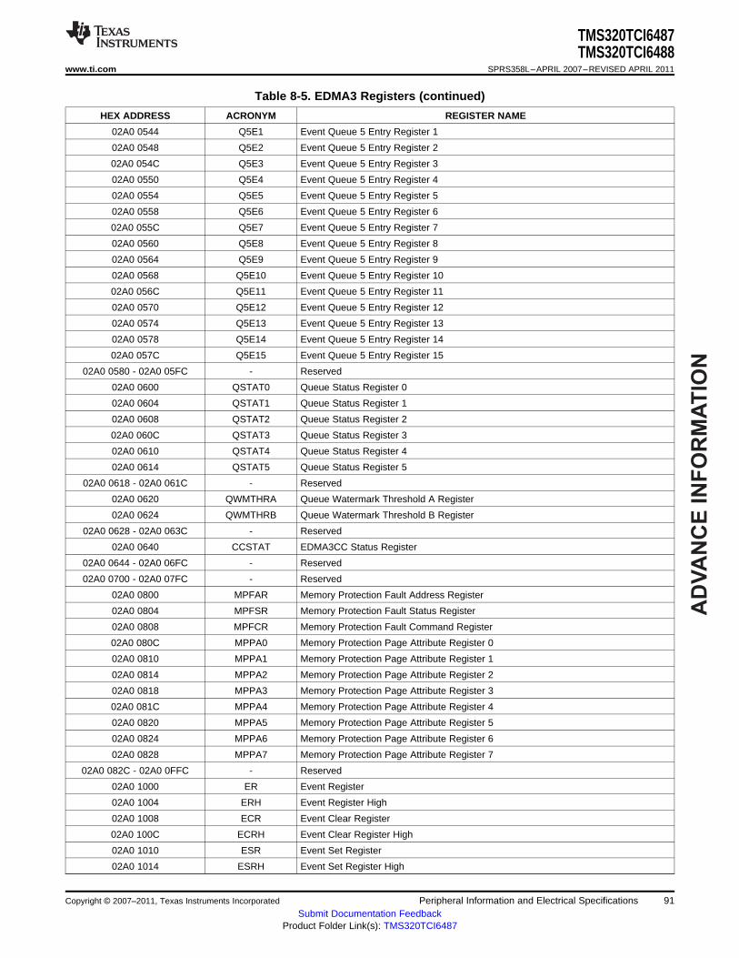
AD
VA
NC
E I
NF
OR
MA
TIO
N
TMS320TCI6487TMS320TCI6488
www.ti.com SPRS358L–APRIL 2007–REVISED APRIL 2011
Table 8-5. EDMA3 Registers (continued)
HEX ADDRESS ACRONYM REGISTER NAME
02A0 0544 Q5E1 Event Queue 5 Entry Register 1
02A0 0548 Q5E2 Event Queue 5 Entry Register 2
02A0 054C Q5E3 Event Queue 5 Entry Register 3
02A0 0550 Q5E4 Event Queue 5 Entry Register 4
02A0 0554 Q5E5 Event Queue 5 Entry Register 5
02A0 0558 Q5E6 Event Queue 5 Entry Register 6
02A0 055C Q5E7 Event Queue 5 Entry Register 7
02A0 0560 Q5E8 Event Queue 5 Entry Register 8
02A0 0564 Q5E9 Event Queue 5 Entry Register 9
02A0 0568 Q5E10 Event Queue 5 Entry Register 10
02A0 056C Q5E11 Event Queue 5 Entry Register 11
02A0 0570 Q5E12 Event Queue 5 Entry Register 12
02A0 0574 Q5E13 Event Queue 5 Entry Register 13
02A0 0578 Q5E14 Event Queue 5 Entry Register 14
02A0 057C Q5E15 Event Queue 5 Entry Register 15
02A0 0580 - 02A0 05FC - Reserved
02A0 0600 QSTAT0 Queue Status Register 0
02A0 0604 QSTAT1 Queue Status Register 1
02A0 0608 QSTAT2 Queue Status Register 2
02A0 060C QSTAT3 Queue Status Register 3
02A0 0610 QSTAT4 Queue Status Register 4
02A0 0614 QSTAT5 Queue Status Register 5
02A0 0618 - 02A0 061C - Reserved
02A0 0620 QWMTHRA Queue Watermark Threshold A Register
02A0 0624 QWMTHRB Queue Watermark Threshold B Register
02A0 0628 - 02A0 063C - Reserved
02A0 0640 CCSTAT EDMA3CC Status Register
02A0 0644 - 02A0 06FC - Reserved
02A0 0700 - 02A0 07FC - Reserved
02A0 0800 MPFAR Memory Protection Fault Address Register
02A0 0804 MPFSR Memory Protection Fault Status Register
02A0 0808 MPFCR Memory Protection Fault Command Register
02A0 080C MPPA0 Memory Protection Page Attribute Register 0
02A0 0810 MPPA1 Memory Protection Page Attribute Register 1
02A0 0814 MPPA2 Memory Protection Page Attribute Register 2
02A0 0818 MPPA3 Memory Protection Page Attribute Register 3
02A0 081C MPPA4 Memory Protection Page Attribute Register 4
02A0 0820 MPPA5 Memory Protection Page Attribute Register 5
02A0 0824 MPPA6 Memory Protection Page Attribute Register 6
02A0 0828 MPPA7 Memory Protection Page Attribute Register 7
02A0 082C - 02A0 0FFC - Reserved
02A0 1000 ER Event Register
02A0 1004 ERH Event Register High
02A0 1008 ECR Event Clear Register
02A0 100C ECRH Event Clear Register High
02A0 1010 ESR Event Set Register
02A0 1014 ESRH Event Set Register High
Copyright © 2007–2011, Texas Instruments Incorporated Peripheral Information and Electrical Specifications 91Submit Documentation Feedback
Product Folder Link(s): TMS320TCI6487
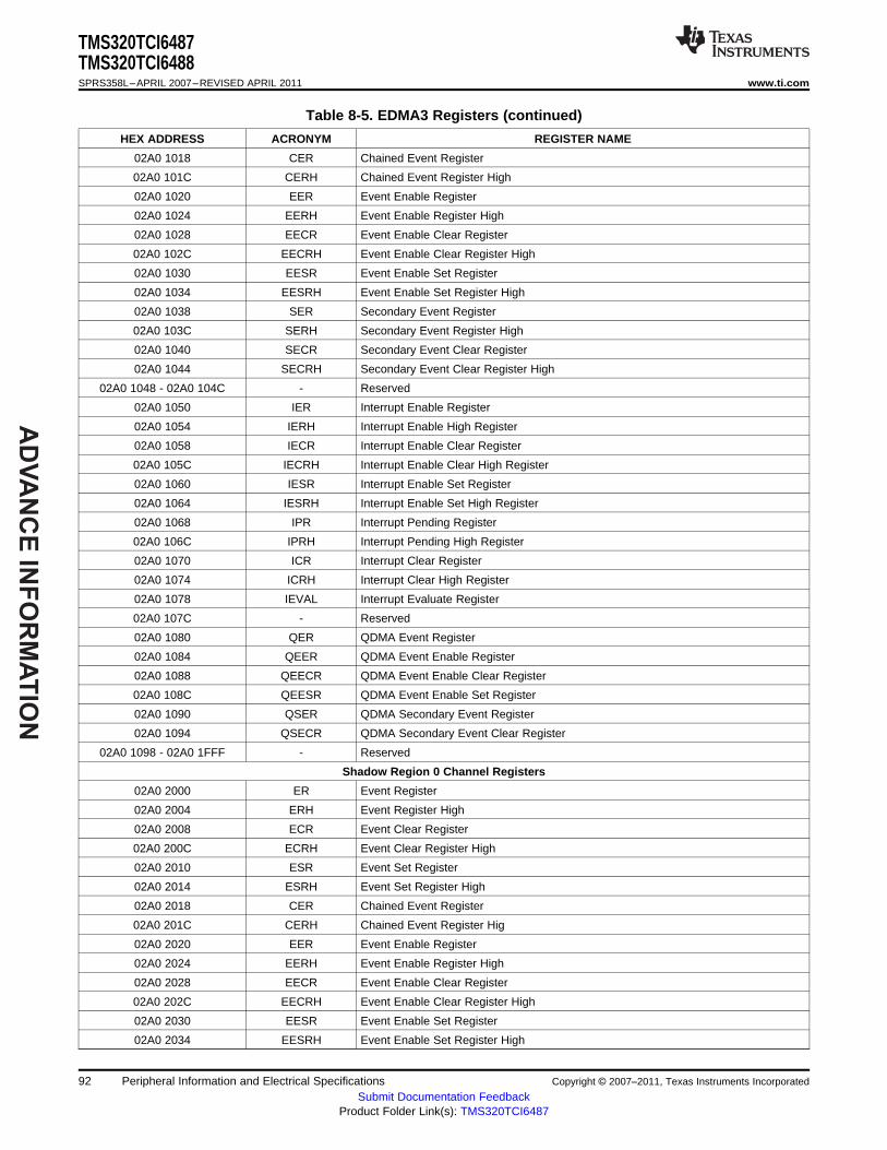
AD
VA
NC
E IN
FO
RM
AT
ION
TMS320TCI6487TMS320TCI6488SPRS358L–APRIL 2007–REVISED APRIL 2011 www.ti.com
Table 8-5. EDMA3 Registers (continued)
HEX ADDRESS ACRONYM REGISTER NAME
02A0 1018 CER Chained Event Register
02A0 101C CERH Chained Event Register High
02A0 1020 EER Event Enable Register
02A0 1024 EERH Event Enable Register High
02A0 1028 EECR Event Enable Clear Register
02A0 102C EECRH Event Enable Clear Register High
02A0 1030 EESR Event Enable Set Register
02A0 1034 EESRH Event Enable Set Register High
02A0 1038 SER Secondary Event Register
02A0 103C SERH Secondary Event Register High
02A0 1040 SECR Secondary Event Clear Register
02A0 1044 SECRH Secondary Event Clear Register High
02A0 1048 - 02A0 104C - Reserved
02A0 1050 IER Interrupt Enable Register
02A0 1054 IERH Interrupt Enable High Register
02A0 1058 IECR Interrupt Enable Clear Register
02A0 105C IECRH Interrupt Enable Clear High Register
02A0 1060 IESR Interrupt Enable Set Register
02A0 1064 IESRH Interrupt Enable Set High Register
02A0 1068 IPR Interrupt Pending Register
02A0 106C IPRH Interrupt Pending High Register
02A0 1070 ICR Interrupt Clear Register
02A0 1074 ICRH Interrupt Clear High Register
02A0 1078 IEVAL Interrupt Evaluate Register
02A0 107C - Reserved
02A0 1080 QER QDMA Event Register
02A0 1084 QEER QDMA Event Enable Register
02A0 1088 QEECR QDMA Event Enable Clear Register
02A0 108C QEESR QDMA Event Enable Set Register
02A0 1090 QSER QDMA Secondary Event Register
02A0 1094 QSECR QDMA Secondary Event Clear Register
02A0 1098 - 02A0 1FFF - Reserved
Shadow Region 0 Channel Registers
02A0 2000 ER Event Register
02A0 2004 ERH Event Register High
02A0 2008 ECR Event Clear Register
02A0 200C ECRH Event Clear Register High
02A0 2010 ESR Event Set Register
02A0 2014 ESRH Event Set Register High
02A0 2018 CER Chained Event Register
02A0 201C CERH Chained Event Register Hig
02A0 2020 EER Event Enable Register
02A0 2024 EERH Event Enable Register High
02A0 2028 EECR Event Enable Clear Register
02A0 202C EECRH Event Enable Clear Register High
02A0 2030 EESR Event Enable Set Register
02A0 2034 EESRH Event Enable Set Register High
92 Peripheral Information and Electrical Specifications Copyright © 2007–2011, Texas Instruments Incorporated
Submit Documentation FeedbackProduct Folder Link(s): TMS320TCI6487

AD
VA
NC
E I
NF
OR
MA
TIO
N
TMS320TCI6487TMS320TCI6488
www.ti.com SPRS358L–APRIL 2007–REVISED APRIL 2011
Table 8-5. EDMA3 Registers (continued)
HEX ADDRESS ACRONYM REGISTER NAME
02A0 2038 SER Secondary Event Register
02A0 203C SERH Secondary Event Register High
02A0 2040 SECR Secondary Event Clear Register
02A0 2044 SECRH Secondary Event Clear Register High
02A0 2048 - 02A0 204C - Reserved
02A0 2050 IER Interrupt Enable Register
02A0 2054 IERH Interrupt Enable Register High
02A0 2058 IECR Interrupt Enable Clear Register
02A0 205C IECRH Interrupt Enable Clear Register High
02A0 2060 IESR Interrupt Enable Set Register
02A0 2064 IESRH Interrupt Enable Set Register High
02A0 2068 IPR Interrupt Pending Register
02A0 206C IPRH Interrupt Pending Register High
02A0 2070 ICR Interrupt Clear Register
02A0 2074 ICRH Interrupt Clear Register High
02A0 2078 IEVAL Interrupt Evaluate Register
02A0 207C - Reserved
02A0 2080 QER QDMA Event Register
02A0 2084 QEER QDMA Event Enable Register
02A0 2088 QEECR QDMA Event Enable Clear Register
02A0 208C QEESR QDMA Event Enable Set Register
02A0 2090 QSER QDMA Secondary Event Register
02A0 2094 QSECR QDMA Secondary Event Clear Register
02A0 2098 - 02A0 21FF - Reserved
Shadow Region 1 Channel Registers
02A0 2200 ER Event Register
02A0 2204 ERH Event Register High
02A0 2208 ECR Event Clear Register
02A0 220C ECRH Event Clear Register High
02A0 2210 ESR Event Set Register
02A0 2214 ESRH Event Set Register High
02A0 2218 CER Chained Event Register
02A0 221C CERH Chained Event Register Hig
02A0 2220 EER Event Enable Register
02A0 2224 EERH Event Enable Register High
02A0 2228 EECR Event Enable Clear Register
02A0 222C EECRH Event Enable Clear Register High
02A0 2230 EESR Event Enable Set Register
02A0 2234 EESRH Event Enable Set Register High
02A0 2238 SER Secondary Event Register
02A0 223C SERH Secondary Event Register High
02A0 2240 SECR Secondary Event Clear Register
02A0 2244 SECRH Secondary Event Clear Register High
02A0 2248 - 02A0 224C - Reserved
02A0 2250 IER Interrupt Enable Register
02A0 2254 IERH Interrupt Enable Register High
02A0 2258 IECR Interrupt Enable Clear Register
Copyright © 2007–2011, Texas Instruments Incorporated Peripheral Information and Electrical Specifications 93Submit Documentation Feedback
Product Folder Link(s): TMS320TCI6487
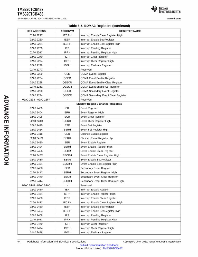
AD
VA
NC
E IN
FO
RM
AT
ION
TMS320TCI6487TMS320TCI6488SPRS358L–APRIL 2007–REVISED APRIL 2011 www.ti.com
Table 8-5. EDMA3 Registers (continued)
HEX ADDRESS ACRONYM REGISTER NAME
02A0 225C IECRH Interrupt Enable Clear Register High
02A0 2260 IESR Interrupt Enable Set Register
02A0 2264 IESRH Interrupt Enable Set Register High
02A0 2268 IPR Interrupt Pending Register
02A0 226C IPRH Interrupt Pending Register High
02A0 2270 ICR Interrupt Clear Register
02A0 2274 ICRH Interrupt Clear Register High
02A0 2278 IEVAL Interrupt Evaluate Register
02A0 227C - Reserved
02A0 2280 QER QDMA Event Register
02A0 2284 QEER QDMA Event Enable Register
02A0 2288 QEECR QDMA Event Enable Clear Register
02A0 228C QEESR QDMA Event Enable Set Register
02A0 2290 QSER QDMA Secondary Event Register
02A0 2294 QSECR QDMA Secondary Event Clear Register
02A0 2298 - 02A0 23FF - Reserved
Shadow Region 2 Channel Registers
02A0 2400 ER Event Register
02A0 2404 ERH Event Register High
02A0 2408 ECR Event Clear Register
02A0 240C ECRH Event Clear Register High
02A0 2410 ESR Event Set Register
02A0 2414 ESRH Event Set Register High
02A0 2418 CER Chained Event Register
02A0 241C CERH Chained Event Register Hig
02A0 2420 EER Event Enable Register
02A0 2424 EERH Event Enable Register High
02A0 2428 EECR Event Enable Clear Register
02A0 242C EECRH Event Enable Clear Register High
02A0 2430 EESR Event Enable Set Register
02A0 2434 EESRH Event Enable Set Register High
02A0 2438 SER Secondary Event Register
02A0 243C SERH Secondary Event Register High
02A0 2440 SECR Secondary Event Clear Register
02A0 2444 SECRH Secondary Event Clear Register High
02A0 2448 - 02A0 244C - Reserved
02A0 2450 IER Interrupt Enable Register
02A0 2454 IERH Interrupt Enable Register High
02A0 2458 IECR Interrupt Enable Clear Register
02A0 245C IECRH Interrupt Enable Clear Register High
02A0 2460 IESR Interrupt Enable Set Register
02A0 2464 IESRH Interrupt Enable Set Register High
02A0 2468 IPR Interrupt Pending Register
02A0 246C IPRH Interrupt Pending Register High
02A0 2470 ICR Interrupt Clear Register
02A0 2474 ICRH Interrupt Clear Register High
02A0 2478 IEVAL Interrupt Evaluate Register
94 Peripheral Information and Electrical Specifications Copyright © 2007–2011, Texas Instruments Incorporated
Submit Documentation FeedbackProduct Folder Link(s): TMS320TCI6487
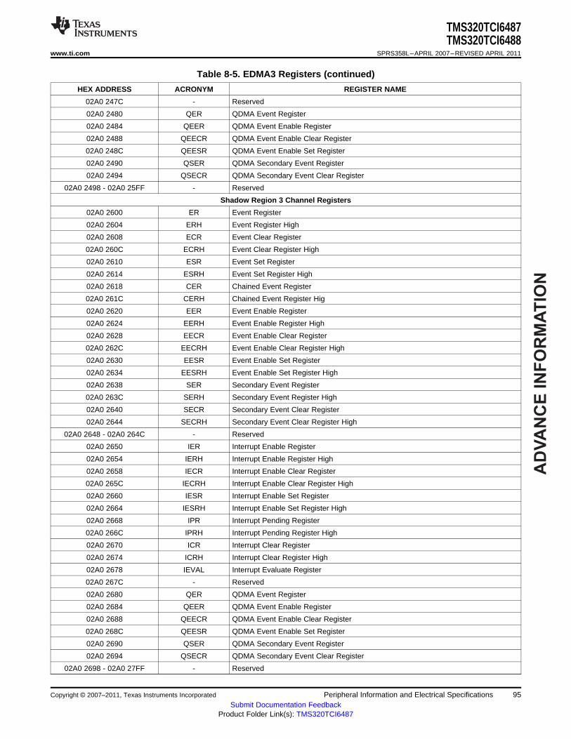
AD
VA
NC
E I
NF
OR
MA
TIO
N
TMS320TCI6487TMS320TCI6488
www.ti.com SPRS358L–APRIL 2007–REVISED APRIL 2011
Table 8-5. EDMA3 Registers (continued)
HEX ADDRESS ACRONYM REGISTER NAME
02A0 247C - Reserved
02A0 2480 QER QDMA Event Register
02A0 2484 QEER QDMA Event Enable Register
02A0 2488 QEECR QDMA Event Enable Clear Register
02A0 248C QEESR QDMA Event Enable Set Register
02A0 2490 QSER QDMA Secondary Event Register
02A0 2494 QSECR QDMA Secondary Event Clear Register
02A0 2498 - 02A0 25FF - Reserved
Shadow Region 3 Channel Registers
02A0 2600 ER Event Register
02A0 2604 ERH Event Register High
02A0 2608 ECR Event Clear Register
02A0 260C ECRH Event Clear Register High
02A0 2610 ESR Event Set Register
02A0 2614 ESRH Event Set Register High
02A0 2618 CER Chained Event Register
02A0 261C CERH Chained Event Register Hig
02A0 2620 EER Event Enable Register
02A0 2624 EERH Event Enable Register High
02A0 2628 EECR Event Enable Clear Register
02A0 262C EECRH Event Enable Clear Register High
02A0 2630 EESR Event Enable Set Register
02A0 2634 EESRH Event Enable Set Register High
02A0 2638 SER Secondary Event Register
02A0 263C SERH Secondary Event Register High
02A0 2640 SECR Secondary Event Clear Register
02A0 2644 SECRH Secondary Event Clear Register High
02A0 2648 - 02A0 264C - Reserved
02A0 2650 IER Interrupt Enable Register
02A0 2654 IERH Interrupt Enable Register High
02A0 2658 IECR Interrupt Enable Clear Register
02A0 265C IECRH Interrupt Enable Clear Register High
02A0 2660 IESR Interrupt Enable Set Register
02A0 2664 IESRH Interrupt Enable Set Register High
02A0 2668 IPR Interrupt Pending Register
02A0 266C IPRH Interrupt Pending Register High
02A0 2670 ICR Interrupt Clear Register
02A0 2674 ICRH Interrupt Clear Register High
02A0 2678 IEVAL Interrupt Evaluate Register
02A0 267C - Reserved
02A0 2680 QER QDMA Event Register
02A0 2684 QEER QDMA Event Enable Register
02A0 2688 QEECR QDMA Event Enable Clear Register
02A0 268C QEESR QDMA Event Enable Set Register
02A0 2690 QSER QDMA Secondary Event Register
02A0 2694 QSECR QDMA Secondary Event Clear Register
02A0 2698 - 02A0 27FF - Reserved
Copyright © 2007–2011, Texas Instruments Incorporated Peripheral Information and Electrical Specifications 95Submit Documentation Feedback
Product Folder Link(s): TMS320TCI6487

AD
VA
NC
E IN
FO
RM
AT
ION
TMS320TCI6487TMS320TCI6488SPRS358L–APRIL 2007–REVISED APRIL 2011 www.ti.com
Table 8-5. EDMA3 Registers (continued)
HEX ADDRESS ACRONYM REGISTER NAME
Shadow Region 4 Channel Registers
02A0 2800 ER Event Register
02A0 2804 ERH Event Register High
02A0 2808 ECR Event Clear Register
02A0 280C ECRH Event Clear Register High
02A0 2810 ESR Event Set Register
02A0 2814 ESRH Event Set Register High
02A0 2818 CER Chained Event Register
02A0 281C CERH Chained Event Register Hig
02A0 2820 EER Event Enable Register
02A0 2824 EERH Event Enable Register High
02A0 2828 EECR Event Enable Clear Register
02A0 282C EECRH Event Enable Clear Register High
02A0 2830 EESR Event Enable Set Register
02A0 2834 EESRH Event Enable Set Register High
02A0 2838 SER Secondary Event Register
02A0 283C SERH Secondary Event Register High
02A0 2840 SECR Secondary Event Clear Register
02A0 2844 SECRH Secondary Event Clear Register High
02A0 2848 - 02A0 284C - Reserved
02A0 2850 IER Interrupt Enable Register
02A0 2854 IERH Interrupt Enable Register High
02A0 2858 IECR Interrupt Enable Clear Register
02A0 285C IECRH Interrupt Enable Clear Register High
02A0 2860 IESR Interrupt Enable Set Register
02A0 2864 IESRH Interrupt Enable Set Register High
02A0 2868 IPR Interrupt Pending Register
02A0 286C IPRH Interrupt Pending Register High
02A0 2870 ICR Interrupt Clear Register
02A0 2874 ICRH Interrupt Clear Register High
02A0 2878 IEVAL Interrupt Evaluate Register
02A0 287C - Reserved
02A0 2880 QER QDMA Event Register
02A0 2884 QEER QDMA Event Enable Register
02A0 2888 QEECR QDMA Event Enable Clear Register
02A0 288C QEESR QDMA Event Enable Set Register
02A0 2890 QSER QDMA Secondary Event Register
02A0 2894 QSECR QDMA Secondary Event Clear Register
02A0 2898 - 02A0 29FF - Reserved
Shadow Region 5 Channel Registers
02A0 2A00 ER Event Register
02A0 2A04 ERH Event Register High
02A0 2A08 ECR Event Clear Register
02A0 2A0C ECRH Event Clear Register High
02A0 2A10 ESR Event Set Register
02A0 2A14 ESRH Event Set Register High
02A0 2A18 CER Chained Event Register
96 Peripheral Information and Electrical Specifications Copyright © 2007–2011, Texas Instruments Incorporated
Submit Documentation FeedbackProduct Folder Link(s): TMS320TCI6487
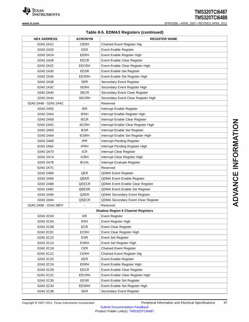
AD
VA
NC
E I
NF
OR
MA
TIO
N
TMS320TCI6487TMS320TCI6488
www.ti.com SPRS358L–APRIL 2007–REVISED APRIL 2011
Table 8-5. EDMA3 Registers (continued)
HEX ADDRESS ACRONYM REGISTER NAME
02A0 2A1C CERH Chained Event Register Hig
02A0 2A20 EER Event Enable Register
02A0 2A24 EERH Event Enable Register High
02A0 2A28 EECR Event Enable Clear Register
02A0 2A2C EECRH Event Enable Clear Register High
02A0 2A30 EESR Event Enable Set Register
02A0 2A34 EESRH Event Enable Set Register High
02A0 2A38 SER Secondary Event Register
02A0 2A3C SERH Secondary Event Register High
02A0 2A40 SECR Secondary Event Clear Register
02A0 2A44 SECRH Secondary Event Clear Register High
02A0 2A48 - 02A0 2A4C - Reserved
02A0 2A50 IER Interrupt Enable Register
02A0 2A54 IERH Interrupt Enable Register High
02A0 2A58 IECR Interrupt Enable Clear Register
02A0 2A5C IECRH Interrupt Enable Clear Register High
02A0 2A60 IESR Interrupt Enable Set Register
02A0 2A64 IESRH Interrupt Enable Set Register High
02A0 2A68 IPR Interrupt Pending Register
02A0 2A6C IPRH Interrupt Pending Register High
02A0 2A70 ICR Interrupt Clear Register
02A0 2A74 ICRH Interrupt Clear Register High
02A0 2A78 IEVAL Interrupt Evaluate Register
02A0 2A7C - Reserved
02A0 2A80 QER QDMA Event Register
02A0 2A84 QEER QDMA Event Enable Register
02A0 2A88 QEECR QDMA Event Enable Clear Register
02A0 2A8C QEESR QDMA Event Enable Set Register
02A0 2A90 QSER QDMA Secondary Event Register
02A0 2A94 QSECR QDMA Secondary Event Clear Register
02A0 2A98 - 02A0 2BFF - Reserved
Shadow Region 6 Channel Registers
02A0 2C00 ER Event Register
02A0 2C04 ERH Event Register High
02A0 2C08 ECR Event Clear Register
02A0 2C0C ECRH Event Clear Register High
02A0 2C10 ESR Event Set Register
02A0 2C14 ESRH Event Set Register High
02A0 2C18 CER Chained Event Register
02A0 2C1C CERH Chained Event Register Hig
02A0 2C20 EER Event Enable Register
02A0 2C24 EERH Event Enable Register High
02A0 2C28 EECR Event Enable Clear Register
02A0 2C2C EECRH Event Enable Clear Register High
02A0 2C30 EESR Event Enable Set Register
02A0 2C34 EESRH Event Enable Set Register High
02A0 2C38 SER Secondary Event Register
Copyright © 2007–2011, Texas Instruments Incorporated Peripheral Information and Electrical Specifications 97Submit Documentation Feedback
Product Folder Link(s): TMS320TCI6487

AD
VA
NC
E IN
FO
RM
AT
ION
TMS320TCI6487TMS320TCI6488SPRS358L–APRIL 2007–REVISED APRIL 2011 www.ti.com
Table 8-5. EDMA3 Registers (continued)
HEX ADDRESS ACRONYM REGISTER NAME
02A0 2C3C SERH Secondary Event Register High
02A0 2C40 SECR Secondary Event Clear Register
02A0 2C44 SECRH Secondary Event Clear Register High
02A0 2C48 - 02A0 2C4C - Reserved
02A0 2C50 IER Interrupt Enable Register
02A0 2C54 IERH Interrupt Enable Register High
02A0 2C58 IECR Interrupt Enable Clear Register
02A0 2C5C IECRH Interrupt Enable Clear Register High
02A0 2C60 IESR Interrupt Enable Set Register
02A0 2C64 IESRH Interrupt Enable Set Register High
02A0 2C68 IPR Interrupt Pending Register
02A0 2C6C IPRH Interrupt Pending Register High
02A0 2C70 ICR Interrupt Clear Register
02A0 2C74 ICRH Interrupt Clear Register High
02A0 2C78 IEVAL Interrupt Evaluate Register
02A0 2C7C - Reserved
02A0 2C80 QER QDMA Event Register
02A0 2C84 QEER QDMA Event Enable Register
02A0 2C88 QEECR QDMA Event Enable Clear Register
02A0 2C8C QEESR QDMA Event Enable Set Register
02A0 2C90 QSER QDMA Secondary Event Register
02A0 2C94 QSECR QDMA Secondary Event Clear Register
02A0 2C98 - 02A0 2DFF - Reserved
Shadow Region 7 Channel Registers
02A0 2E00 ER Event Register
02A0 2E04 ERH Event Register High
02A0 2E08 ECR Event Clear Register
02A0 2E0C ECRH Event Clear Register High
02A0 2E10 ESR Event Set Register
02A0 2E14 ESRH Event Set Register High
02A0 2E18 CER Chained Event Register
02A0 2E1C CERH Chained Event Register Hig
02A0 2E20 EER Event Enable Register
02A0 2E24 EERH Event Enable Register High
02A0 2E28 EECR Event Enable Clear Register
02A0 2E2C EECRH Event Enable Clear Register High
02A0 2E30 EESR Event Enable Set Register
02A0 2E34 EESRH Event Enable Set Register High
02A0 2E38 SER Secondary Event Register
02A0 2E3C SERH Secondary Event Register High
02A0 2E40 SECR Secondary Event Clear Register
02A0 2E44 SECRH Secondary Event Clear Register High
02A0 2E48 - 02A0 2E4C - Reserved
02A0 2E50 IER Interrupt Enable Register
02A0 2E54 IERH Interrupt Enable Register High
02A0 2E58 IECR Interrupt Enable Clear Register
02A0 2E5C IECRH Interrupt Enable Clear Register High
98 Peripheral Information and Electrical Specifications Copyright © 2007–2011, Texas Instruments Incorporated
Submit Documentation FeedbackProduct Folder Link(s): TMS320TCI6487

AD
VA
NC
E I
NF
OR
MA
TIO
N
TMS320TCI6487TMS320TCI6488
www.ti.com SPRS358L–APRIL 2007–REVISED APRIL 2011
Table 8-5. EDMA3 Registers (continued)
HEX ADDRESS ACRONYM REGISTER NAME
02A0 2E60 IESR Interrupt Enable Set Register
02A0 2E64 IESRH Interrupt Enable Set Register High
02A0 2E68 IPR Interrupt Pending Register
02A0 2E6C IPRH Interrupt Pending Register High
02A0 2E70 ICR Interrupt Clear Register
02A0 2E74 ICRH Interrupt Clear Register High
02A0 2E78 IEVAL Interrupt Evaluate Register
02A0 2E7C - Reserved
02A0 2E80 QER QDMA Event Register
02A0 2E84 QEER QDMA Event Enable Register
02A0 2E88 QEECR QDMA Event Enable Clear Register
02A0 2E8C QEESR QDMA Event Enable Set Register
02A0 2E90 QSER QDMA Secondary Event Register
02A0 2E94 QSECR QDMA Secondary Event Clear Register
02A0 2E98 - 02A0 2FFF - Reserved
Copyright © 2007–2011, Texas Instruments Incorporated Peripheral Information and Electrical Specifications 99Submit Documentation Feedback
Product Folder Link(s): TMS320TCI6487

AD
VA
NC
E IN
FO
RM
AT
ION
TMS320TCI6487TMS320TCI6488SPRS358L–APRIL 2007–REVISED APRIL 2011 www.ti.com
Table 8-6. EDMA3 Parameter RAM
HEX ADDRESS ACRONYM REGISTER NAME
02A0 4000 - 02A0 401F Parameter Set 0
02A0 4020 - 02A0 403F Parameter Set 1
02A0 4040 - 02A0 405F Parameter Set 2
02A0 4060 - 02A0 407F Parameter Set 3
02A0 4080 - 02A0 409F Parameter Set 4
02A0 40A0 - 02A0 40BF Parameter Set 5
02A0 40C0 - 02A0 40DF Parameter Set 6
02A0 40E0 - 02A0 40FF Parameter Set 7
02A0 4100 - 02A0 411F Parameter Set 8
02A0 4120 - 02A0 413F Parameter Set 9
... ...
02A0 47E0 - 02A0 47FF Parameter Set 63
02A0 4800 - 02A0 481F Parameter Set 64
02A0 4820 - 02A0 483F Parameter Set 65
... ...
02A0 5FC0 - 02A0 5FDF Parameter Set 254
02A0 5FE0 - 02A0 5FFF Parameter Set 255
Table 8-7. EDMA3 Transfer Controller 0 Registers
HEX ADDRESS RANGE ACRONYM REGISTER NAME
02A2 0000 PID Peripheral Identification Register
02A2 0004 TCCFG EDMA3TC Configuration Register
02A2 0008 - 02A2 00FC - Reserved
02A2 0100 TCSTAT EDMA3TC Channel Status Register
02A2 0104 - 02A2 011C - Reserved
02A2 0120 ERRSTAT Error Register
02A2 0124 ERREN Error Enable Register
02A2 0128 ERRCLR Error Clear Register
02A2 012C ERRDET Error Details Register
02A2 0130 ERRCMD Error Interrupt Command Register
02A2 0134 - 02A2 013C - Reserved
02A2 0140 RDRATE Read Rate Register
02A2 0144 - 02A2 023C - Reserved
02A2 0240 SAOPT Source Active Options Register
02A2 0244 SASRC Source Active Source Address Register
02A2 0248 SACNT Source Active Count Register
02A2 024C SADST Source Active Destination Address Register
02A2 0250 SABIDX Source Active Source B-Index Register
02A2 0254 SAMPPRXY Source Active Memory Protection Proxy Register
02A2 0258 SACNTRLD Source Active Count Reload Register
02A2 025C SASRCBREF Source Active Source Address B-Reference Register
02A2 0260 SADSTBREF Source Active Destination Address B-Reference Register
02A2 0264 - 02A2 027C - Reserved
02A2 0280 DFCNTRLD Destination FIFO Set Count Reload
02A2 0284 DFSRCBREF Destination FIFO Set Destination Address B Reference Register
02A2 0288 DFDSTBREF Destination FIFO Set Destination Address B Reference Register
02A2 028C - 02A2 02FC - Reserved
100 Peripheral Information and Electrical Specifications Copyright © 2007–2011, Texas Instruments Incorporated
Submit Documentation FeedbackProduct Folder Link(s): TMS320TCI6487

AD
VA
NC
E I
NF
OR
MA
TIO
N
TMS320TCI6487TMS320TCI6488
www.ti.com SPRS358L–APRIL 2007–REVISED APRIL 2011
Table 8-7. EDMA3 Transfer Controller 0 Registers (continued)
HEX ADDRESS RANGE ACRONYM REGISTER NAME
02A2 0300 DFOPT0 Destination FIFO Options Register 0
02A2 0304 DFSRC0 Destination FIFO Source Address Register 0
02A2 0308 DFCNT0 Destination FIFO Count Register 0
02A2 030C DFDST0 Destination FIFO Destination Address Register 0
02A2 0310 DFBIDX0 Destination FIFO BIDX Register 0
02A2 0314 DFMPPRXY0 Destination FIFO Memory Protection Proxy Register 0
02A2 0318 - 02A2 033C - Reserved
02A2 0340 DFOPT1 Destination FIFO Options Register 1
02A2 0344 DFSRC1 Destination FIFO Source Address Register 1
02A2 0348 DFCNT1 Destination FIFO Count Register 1
02A2 034C DFDST1 Destination FIFO Destination Address Register 1
02A2 0350 DFBIDX1 Destination FIFO BIDX Register 1
02A2 0354 DFMPPRXY1 Destination FIFO Memory Protection Proxy Register 1
02A2 0358 - 02A2 037C - Reserved
02A2 0380 DFOPT2 Destination FIFO Options Register 2
02A2 0384 DFSRC2 Destination FIFO Source Address Register 2
02A2 0388 DFCNT2 Destination FIFO Count Register 2
02A2 038C DFDST2 Destination FIFO Destination Address Register 2
02A2 0390 DFBIDX2 Destination FIFO BIDX Register 2
02A2 0394 DFMPPRXY2 Destination FIFO Memory Protection Proxy Register 2
02A2 0398 - 02A2 03BC - Reserved
02A2 03C0 DFOPT3 Destination FIFO Options Register 3
02A2 03C4 DFSRC3 Destination FIFO Source Address Register 3
02A2 03C8 DFCNT3 Destination FIFO Count Register 3
02A2 03CC DFDST3 Destination FIFO Destination Address Register 3
02A2 03D0 DFBIDX3 Destination FIFO BIDX Register 3
02A2 03D4 DFMPPRXY3 Destination FIFO Memory Protection Proxy Register 3
02A2 03D8 - 02A2 7FFC - Reserved
Table 8-8. EDMA3 Transfer Controller 1 Registers
HEX ADDRESS RANGE ACRONYM REGISTER NAME
02A2 8000 PID Peripheral Identification Register
02A2 8004 TCCFG EDMA3TC Configuration Register
02A2 8008 - 02A2 80FC - Reserved
02A2 8100 TCSTAT EDMA3TC Channel Status Register
02A2 8104 - 02A2 811C - Reserved
02A2 8120 ERRSTAT Error Register
02A2 8124 ERREN Error Enable Register
02A2 8128 ERRCLR Error Clear Register
02A2 812C ERRDET Error Details Register
02A2 8130 ERRCMD Error Interrupt Command Register
02A2 8134 - 02A2 813C - Reserved
02A2 8140 RDRATE Read Rate Register
02A2 8144 - 02A2 823C - Reserved
02A2 8240 SAOPT Source Active Options Register
02A2 8244 SASRC Source Active Source Address Register
02A2 8248 SACNT Source Active Count Register
Copyright © 2007–2011, Texas Instruments Incorporated Peripheral Information and Electrical Specifications 101Submit Documentation Feedback
Product Folder Link(s): TMS320TCI6487
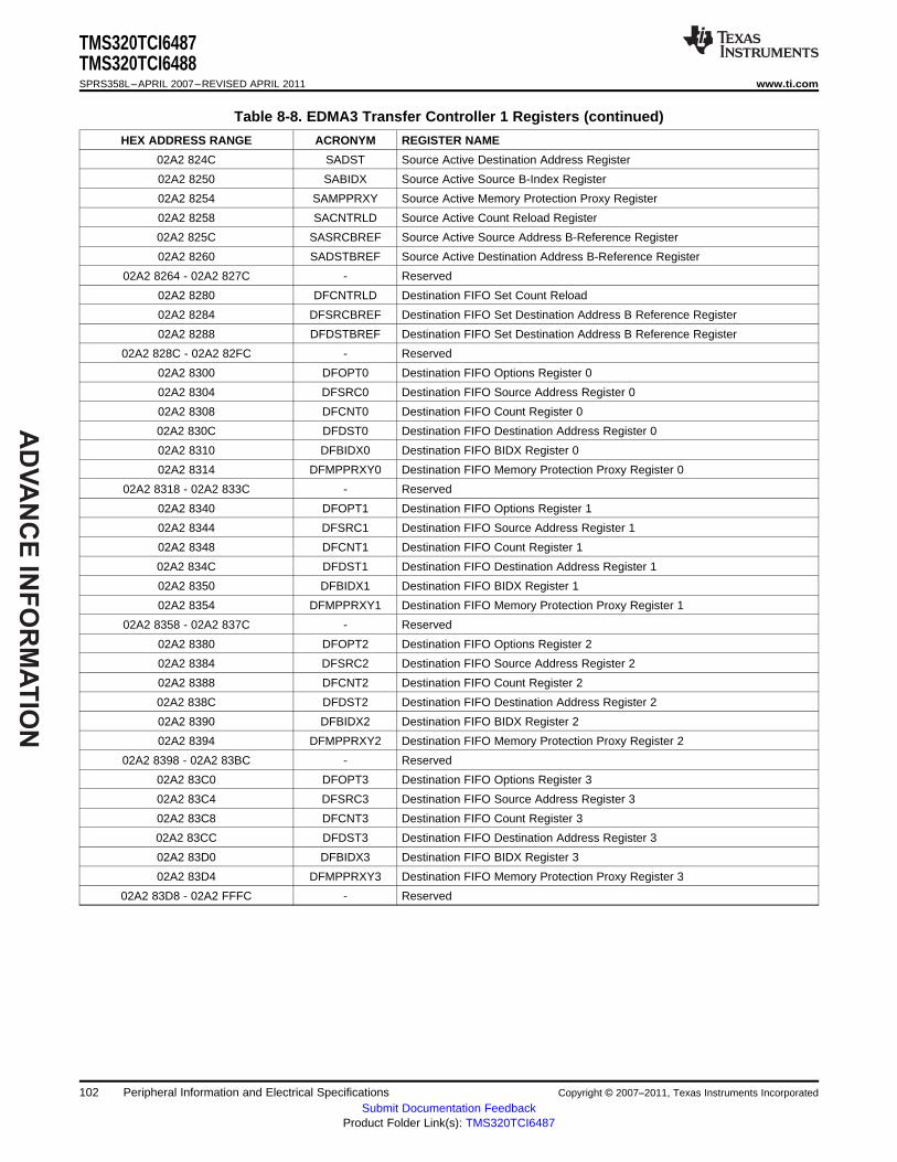
AD
VA
NC
E IN
FO
RM
AT
ION
TMS320TCI6487TMS320TCI6488SPRS358L–APRIL 2007–REVISED APRIL 2011 www.ti.com
Table 8-8. EDMA3 Transfer Controller 1 Registers (continued)
HEX ADDRESS RANGE ACRONYM REGISTER NAME
02A2 824C SADST Source Active Destination Address Register
02A2 8250 SABIDX Source Active Source B-Index Register
02A2 8254 SAMPPRXY Source Active Memory Protection Proxy Register
02A2 8258 SACNTRLD Source Active Count Reload Register
02A2 825C SASRCBREF Source Active Source Address B-Reference Register
02A2 8260 SADSTBREF Source Active Destination Address B-Reference Register
02A2 8264 - 02A2 827C - Reserved
02A2 8280 DFCNTRLD Destination FIFO Set Count Reload
02A2 8284 DFSRCBREF Destination FIFO Set Destination Address B Reference Register
02A2 8288 DFDSTBREF Destination FIFO Set Destination Address B Reference Register
02A2 828C - 02A2 82FC - Reserved
02A2 8300 DFOPT0 Destination FIFO Options Register 0
02A2 8304 DFSRC0 Destination FIFO Source Address Register 0
02A2 8308 DFCNT0 Destination FIFO Count Register 0
02A2 830C DFDST0 Destination FIFO Destination Address Register 0
02A2 8310 DFBIDX0 Destination FIFO BIDX Register 0
02A2 8314 DFMPPRXY0 Destination FIFO Memory Protection Proxy Register 0
02A2 8318 - 02A2 833C - Reserved
02A2 8340 DFOPT1 Destination FIFO Options Register 1
02A2 8344 DFSRC1 Destination FIFO Source Address Register 1
02A2 8348 DFCNT1 Destination FIFO Count Register 1
02A2 834C DFDST1 Destination FIFO Destination Address Register 1
02A2 8350 DFBIDX1 Destination FIFO BIDX Register 1
02A2 8354 DFMPPRXY1 Destination FIFO Memory Protection Proxy Register 1
02A2 8358 - 02A2 837C - Reserved
02A2 8380 DFOPT2 Destination FIFO Options Register 2
02A2 8384 DFSRC2 Destination FIFO Source Address Register 2
02A2 8388 DFCNT2 Destination FIFO Count Register 2
02A2 838C DFDST2 Destination FIFO Destination Address Register 2
02A2 8390 DFBIDX2 Destination FIFO BIDX Register 2
02A2 8394 DFMPPRXY2 Destination FIFO Memory Protection Proxy Register 2
02A2 8398 - 02A2 83BC - Reserved
02A2 83C0 DFOPT3 Destination FIFO Options Register 3
02A2 83C4 DFSRC3 Destination FIFO Source Address Register 3
02A2 83C8 DFCNT3 Destination FIFO Count Register 3
02A2 83CC DFDST3 Destination FIFO Destination Address Register 3
02A2 83D0 DFBIDX3 Destination FIFO BIDX Register 3
02A2 83D4 DFMPPRXY3 Destination FIFO Memory Protection Proxy Register 3
02A2 83D8 - 02A2 FFFC - Reserved
102 Peripheral Information and Electrical Specifications Copyright © 2007–2011, Texas Instruments Incorporated
Submit Documentation FeedbackProduct Folder Link(s): TMS320TCI6487
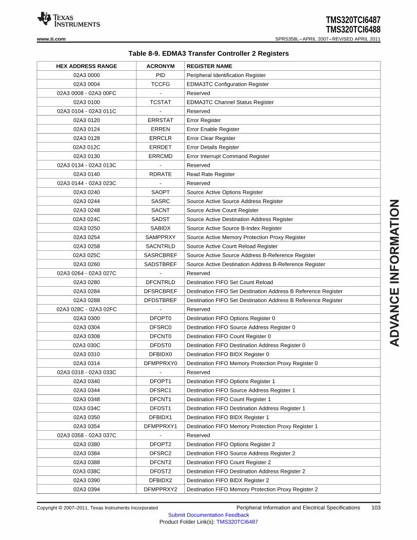
AD
VA
NC
E I
NF
OR
MA
TIO
N
TMS320TCI6487TMS320TCI6488
www.ti.com SPRS358L–APRIL 2007–REVISED APRIL 2011
Table 8-9. EDMA3 Transfer Controller 2 Registers
HEX ADDRESS RANGE ACRONYM REGISTER NAME
02A3 0000 PID Peripheral Identification Register
02A3 0004 TCCFG EDMA3TC Configuration Register
02A3 0008 - 02A3 00FC - Reserved
02A3 0100 TCSTAT EDMA3TC Channel Status Register
02A3 0104 - 02A3 011C - Reserved
02A3 0120 ERRSTAT Error Register
02A3 0124 ERREN Error Enable Register
02A3 0128 ERRCLR Error Clear Register
02A3 012C ERRDET Error Details Register
02A3 0130 ERRCMD Error Interrupt Command Register
02A3 0134 - 02A3 013C - Reserved
02A3 0140 RDRATE Read Rate Register
02A3 0144 - 02A3 023C - Reserved
02A3 0240 SAOPT Source Active Options Register
02A3 0244 SASRC Source Active Source Address Register
02A3 0248 SACNT Source Active Count Register
02A3 024C SADST Source Active Destination Address Register
02A3 0250 SABIDX Source Active Source B-Index Register
02A3 0254 SAMPPRXY Source Active Memory Protection Proxy Register
02A3 0258 SACNTRLD Source Active Count Reload Register
02A3 025C SASRCBREF Source Active Source Address B-Reference Register
02A3 0260 SADSTBREF Source Active Destination Address B-Reference Register
02A3 0264 - 02A3 027C - Reserved
02A3 0280 DFCNTRLD Destination FIFO Set Count Reload
02A3 0284 DFSRCBREF Destination FIFO Set Destination Address B Reference Register
02A3 0288 DFDSTBREF Destination FIFO Set Destination Address B Reference Register
02A3 028C - 02A3 02FC - Reserved
02A3 0300 DFOPT0 Destination FIFO Options Register 0
02A3 0304 DFSRC0 Destination FIFO Source Address Register 0
02A3 0308 DFCNT0 Destination FIFO Count Register 0
02A3 030C DFDST0 Destination FIFO Destination Address Register 0
02A3 0310 DFBIDX0 Destination FIFO BIDX Register 0
02A3 0314 DFMPPRXY0 Destination FIFO Memory Protection Proxy Register 0
02A3 0318 - 02A3 033C - Reserved
02A3 0340 DFOPT1 Destination FIFO Options Register 1
02A3 0344 DFSRC1 Destination FIFO Source Address Register 1
02A3 0348 DFCNT1 Destination FIFO Count Register 1
02A3 034C DFDST1 Destination FIFO Destination Address Register 1
02A3 0350 DFBIDX1 Destination FIFO BIDX Register 1
02A3 0354 DFMPPRXY1 Destination FIFO Memory Protection Proxy Register 1
02A3 0358 - 02A3 037C - Reserved
02A3 0380 DFOPT2 Destination FIFO Options Register 2
02A3 0384 DFSRC2 Destination FIFO Source Address Register 2
02A3 0388 DFCNT2 Destination FIFO Count Register 2
02A3 038C DFDST2 Destination FIFO Destination Address Register 2
02A3 0390 DFBIDX2 Destination FIFO BIDX Register 2
02A3 0394 DFMPPRXY2 Destination FIFO Memory Protection Proxy Register 2
Copyright © 2007–2011, Texas Instruments Incorporated Peripheral Information and Electrical Specifications 103Submit Documentation Feedback
Product Folder Link(s): TMS320TCI6487
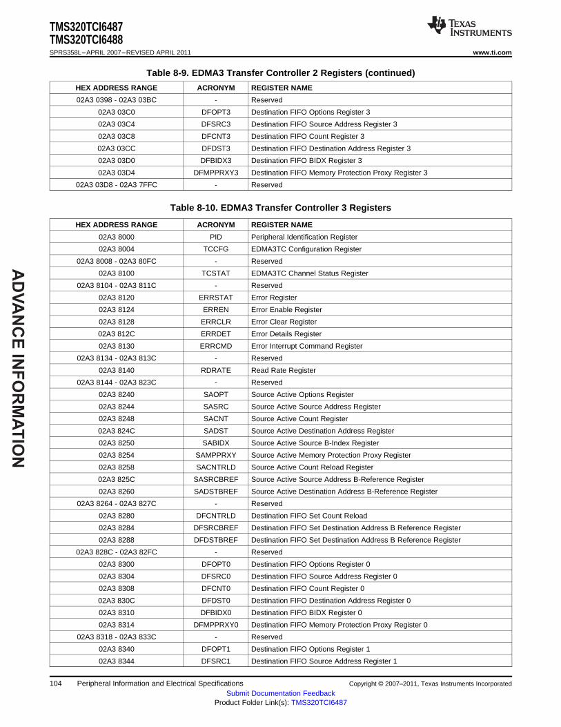
AD
VA
NC
E IN
FO
RM
AT
ION
TMS320TCI6487TMS320TCI6488SPRS358L–APRIL 2007–REVISED APRIL 2011 www.ti.com
Table 8-9. EDMA3 Transfer Controller 2 Registers (continued)
HEX ADDRESS RANGE ACRONYM REGISTER NAME
02A3 0398 - 02A3 03BC - Reserved
02A3 03C0 DFOPT3 Destination FIFO Options Register 3
02A3 03C4 DFSRC3 Destination FIFO Source Address Register 3
02A3 03C8 DFCNT3 Destination FIFO Count Register 3
02A3 03CC DFDST3 Destination FIFO Destination Address Register 3
02A3 03D0 DFBIDX3 Destination FIFO BIDX Register 3
02A3 03D4 DFMPPRXY3 Destination FIFO Memory Protection Proxy Register 3
02A3 03D8 - 02A3 7FFC - Reserved
Table 8-10. EDMA3 Transfer Controller 3 Registers
HEX ADDRESS RANGE ACRONYM REGISTER NAME
02A3 8000 PID Peripheral Identification Register
02A3 8004 TCCFG EDMA3TC Configuration Register
02A3 8008 - 02A3 80FC - Reserved
02A3 8100 TCSTAT EDMA3TC Channel Status Register
02A3 8104 - 02A3 811C - Reserved
02A3 8120 ERRSTAT Error Register
02A3 8124 ERREN Error Enable Register
02A3 8128 ERRCLR Error Clear Register
02A3 812C ERRDET Error Details Register
02A3 8130 ERRCMD Error Interrupt Command Register
02A3 8134 - 02A3 813C - Reserved
02A3 8140 RDRATE Read Rate Register
02A3 8144 - 02A3 823C - Reserved
02A3 8240 SAOPT Source Active Options Register
02A3 8244 SASRC Source Active Source Address Register
02A3 8248 SACNT Source Active Count Register
02A3 824C SADST Source Active Destination Address Register
02A3 8250 SABIDX Source Active Source B-Index Register
02A3 8254 SAMPPRXY Source Active Memory Protection Proxy Register
02A3 8258 SACNTRLD Source Active Count Reload Register
02A3 825C SASRCBREF Source Active Source Address B-Reference Register
02A3 8260 SADSTBREF Source Active Destination Address B-Reference Register
02A3 8264 - 02A3 827C - Reserved
02A3 8280 DFCNTRLD Destination FIFO Set Count Reload
02A3 8284 DFSRCBREF Destination FIFO Set Destination Address B Reference Register
02A3 8288 DFDSTBREF Destination FIFO Set Destination Address B Reference Register
02A3 828C - 02A3 82FC - Reserved
02A3 8300 DFOPT0 Destination FIFO Options Register 0
02A3 8304 DFSRC0 Destination FIFO Source Address Register 0
02A3 8308 DFCNT0 Destination FIFO Count Register 0
02A3 830C DFDST0 Destination FIFO Destination Address Register 0
02A3 8310 DFBIDX0 Destination FIFO BIDX Register 0
02A3 8314 DFMPPRXY0 Destination FIFO Memory Protection Proxy Register 0
02A3 8318 - 02A3 833C - Reserved
02A3 8340 DFOPT1 Destination FIFO Options Register 1
02A3 8344 DFSRC1 Destination FIFO Source Address Register 1
104 Peripheral Information and Electrical Specifications Copyright © 2007–2011, Texas Instruments Incorporated
Submit Documentation FeedbackProduct Folder Link(s): TMS320TCI6487
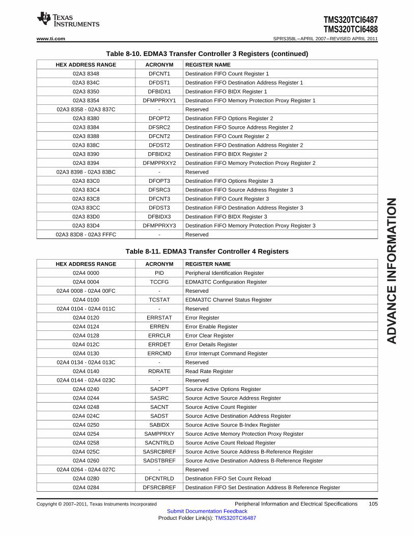
AD
VA
NC
E I
NF
OR
MA
TIO
N
TMS320TCI6487TMS320TCI6488
www.ti.com SPRS358L–APRIL 2007–REVISED APRIL 2011
Table 8-10. EDMA3 Transfer Controller 3 Registers (continued)
HEX ADDRESS RANGE ACRONYM REGISTER NAME
02A3 8348 DFCNT1 Destination FIFO Count Register 1
02A3 834C DFDST1 Destination FIFO Destination Address Register 1
02A3 8350 DFBIDX1 Destination FIFO BIDX Register 1
02A3 8354 DFMPPRXY1 Destination FIFO Memory Protection Proxy Register 1
02A3 8358 - 02A3 837C - Reserved
02A3 8380 DFOPT2 Destination FIFO Options Register 2
02A3 8384 DFSRC2 Destination FIFO Source Address Register 2
02A3 8388 DFCNT2 Destination FIFO Count Register 2
02A3 838C DFDST2 Destination FIFO Destination Address Register 2
02A3 8390 DFBIDX2 Destination FIFO BIDX Register 2
02A3 8394 DFMPPRXY2 Destination FIFO Memory Protection Proxy Register 2
02A3 8398 - 02A3 83BC - Reserved
02A3 83C0 DFOPT3 Destination FIFO Options Register 3
02A3 83C4 DFSRC3 Destination FIFO Source Address Register 3
02A3 83C8 DFCNT3 Destination FIFO Count Register 3
02A3 83CC DFDST3 Destination FIFO Destination Address Register 3
02A3 83D0 DFBIDX3 Destination FIFO BIDX Register 3
02A3 83D4 DFMPPRXY3 Destination FIFO Memory Protection Proxy Register 3
02A3 83D8 - 02A3 FFFC - Reserved
Table 8-11. EDMA3 Transfer Controller 4 Registers
HEX ADDRESS RANGE ACRONYM REGISTER NAME
02A4 0000 PID Peripheral Identification Register
02A4 0004 TCCFG EDMA3TC Configuration Register
02A4 0008 - 02A4 00FC - Reserved
02A4 0100 TCSTAT EDMA3TC Channel Status Register
02A4 0104 - 02A4 011C - Reserved
02A4 0120 ERRSTAT Error Register
02A4 0124 ERREN Error Enable Register
02A4 0128 ERRCLR Error Clear Register
02A4 012C ERRDET Error Details Register
02A4 0130 ERRCMD Error Interrupt Command Register
02A4 0134 - 02A4 013C - Reserved
02A4 0140 RDRATE Read Rate Register
02A4 0144 - 02A4 023C - Reserved
02A4 0240 SAOPT Source Active Options Register
02A4 0244 SASRC Source Active Source Address Register
02A4 0248 SACNT Source Active Count Register
02A4 024C SADST Source Active Destination Address Register
02A4 0250 SABIDX Source Active Source B-Index Register
02A4 0254 SAMPPRXY Source Active Memory Protection Proxy Register
02A4 0258 SACNTRLD Source Active Count Reload Register
02A4 025C SASRCBREF Source Active Source Address B-Reference Register
02A4 0260 SADSTBREF Source Active Destination Address B-Reference Register
02A4 0264 - 02A4 027C - Reserved
02A4 0280 DFCNTRLD Destination FIFO Set Count Reload
02A4 0284 DFSRCBREF Destination FIFO Set Destination Address B Reference Register
Copyright © 2007–2011, Texas Instruments Incorporated Peripheral Information and Electrical Specifications 105Submit Documentation Feedback
Product Folder Link(s): TMS320TCI6487
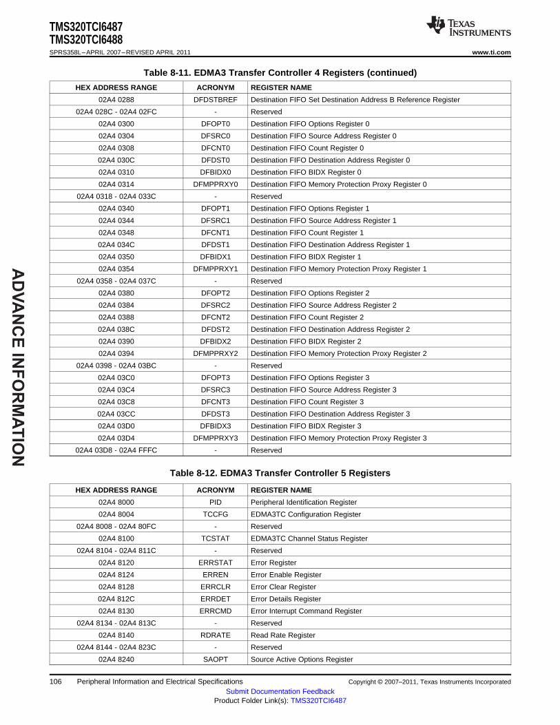
AD
VA
NC
E IN
FO
RM
AT
ION
TMS320TCI6487TMS320TCI6488SPRS358L–APRIL 2007–REVISED APRIL 2011 www.ti.com
Table 8-11. EDMA3 Transfer Controller 4 Registers (continued)
HEX ADDRESS RANGE ACRONYM REGISTER NAME
02A4 0288 DFDSTBREF Destination FIFO Set Destination Address B Reference Register
02A4 028C - 02A4 02FC - Reserved
02A4 0300 DFOPT0 Destination FIFO Options Register 0
02A4 0304 DFSRC0 Destination FIFO Source Address Register 0
02A4 0308 DFCNT0 Destination FIFO Count Register 0
02A4 030C DFDST0 Destination FIFO Destination Address Register 0
02A4 0310 DFBIDX0 Destination FIFO BIDX Register 0
02A4 0314 DFMPPRXY0 Destination FIFO Memory Protection Proxy Register 0
02A4 0318 - 02A4 033C - Reserved
02A4 0340 DFOPT1 Destination FIFO Options Register 1
02A4 0344 DFSRC1 Destination FIFO Source Address Register 1
02A4 0348 DFCNT1 Destination FIFO Count Register 1
02A4 034C DFDST1 Destination FIFO Destination Address Register 1
02A4 0350 DFBIDX1 Destination FIFO BIDX Register 1
02A4 0354 DFMPPRXY1 Destination FIFO Memory Protection Proxy Register 1
02A4 0358 - 02A4 037C - Reserved
02A4 0380 DFOPT2 Destination FIFO Options Register 2
02A4 0384 DFSRC2 Destination FIFO Source Address Register 2
02A4 0388 DFCNT2 Destination FIFO Count Register 2
02A4 038C DFDST2 Destination FIFO Destination Address Register 2
02A4 0390 DFBIDX2 Destination FIFO BIDX Register 2
02A4 0394 DFMPPRXY2 Destination FIFO Memory Protection Proxy Register 2
02A4 0398 - 02A4 03BC - Reserved
02A4 03C0 DFOPT3 Destination FIFO Options Register 3
02A4 03C4 DFSRC3 Destination FIFO Source Address Register 3
02A4 03C8 DFCNT3 Destination FIFO Count Register 3
02A4 03CC DFDST3 Destination FIFO Destination Address Register 3
02A4 03D0 DFBIDX3 Destination FIFO BIDX Register 3
02A4 03D4 DFMPPRXY3 Destination FIFO Memory Protection Proxy Register 3
02A4 03D8 - 02A4 FFFC - Reserved
Table 8-12. EDMA3 Transfer Controller 5 Registers
HEX ADDRESS RANGE ACRONYM REGISTER NAME
02A4 8000 PID Peripheral Identification Register
02A4 8004 TCCFG EDMA3TC Configuration Register
02A4 8008 - 02A4 80FC - Reserved
02A4 8100 TCSTAT EDMA3TC Channel Status Register
02A4 8104 - 02A4 811C - Reserved
02A4 8120 ERRSTAT Error Register
02A4 8124 ERREN Error Enable Register
02A4 8128 ERRCLR Error Clear Register
02A4 812C ERRDET Error Details Register
02A4 8130 ERRCMD Error Interrupt Command Register
02A4 8134 - 02A4 813C - Reserved
02A4 8140 RDRATE Read Rate Register
02A4 8144 - 02A4 823C - Reserved
02A4 8240 SAOPT Source Active Options Register
106 Peripheral Information and Electrical Specifications Copyright © 2007–2011, Texas Instruments Incorporated
Submit Documentation FeedbackProduct Folder Link(s): TMS320TCI6487
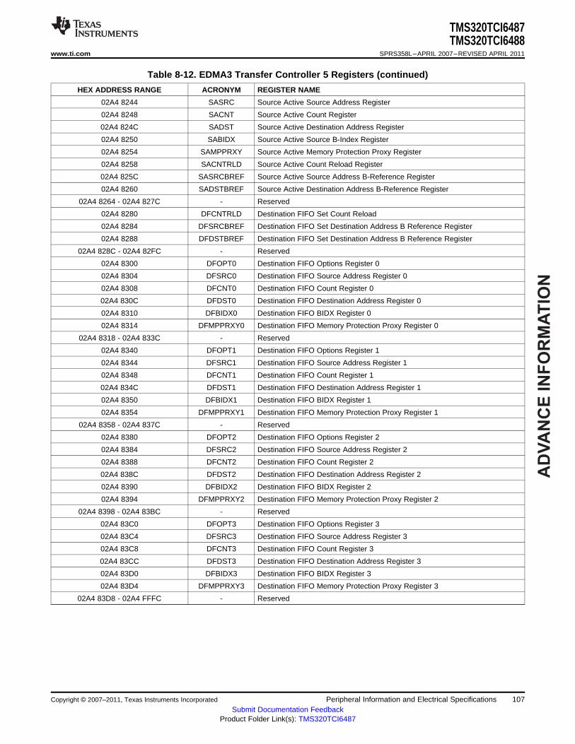
AD
VA
NC
E I
NF
OR
MA
TIO
N
TMS320TCI6487TMS320TCI6488
www.ti.com SPRS358L–APRIL 2007–REVISED APRIL 2011
Table 8-12. EDMA3 Transfer Controller 5 Registers (continued)
HEX ADDRESS RANGE ACRONYM REGISTER NAME
02A4 8244 SASRC Source Active Source Address Register
02A4 8248 SACNT Source Active Count Register
02A4 824C SADST Source Active Destination Address Register
02A4 8250 SABIDX Source Active Source B-Index Register
02A4 8254 SAMPPRXY Source Active Memory Protection Proxy Register
02A4 8258 SACNTRLD Source Active Count Reload Register
02A4 825C SASRCBREF Source Active Source Address B-Reference Register
02A4 8260 SADSTBREF Source Active Destination Address B-Reference Register
02A4 8264 - 02A4 827C - Reserved
02A4 8280 DFCNTRLD Destination FIFO Set Count Reload
02A4 8284 DFSRCBREF Destination FIFO Set Destination Address B Reference Register
02A4 8288 DFDSTBREF Destination FIFO Set Destination Address B Reference Register
02A4 828C - 02A4 82FC - Reserved
02A4 8300 DFOPT0 Destination FIFO Options Register 0
02A4 8304 DFSRC0 Destination FIFO Source Address Register 0
02A4 8308 DFCNT0 Destination FIFO Count Register 0
02A4 830C DFDST0 Destination FIFO Destination Address Register 0
02A4 8310 DFBIDX0 Destination FIFO BIDX Register 0
02A4 8314 DFMPPRXY0 Destination FIFO Memory Protection Proxy Register 0
02A4 8318 - 02A4 833C - Reserved
02A4 8340 DFOPT1 Destination FIFO Options Register 1
02A4 8344 DFSRC1 Destination FIFO Source Address Register 1
02A4 8348 DFCNT1 Destination FIFO Count Register 1
02A4 834C DFDST1 Destination FIFO Destination Address Register 1
02A4 8350 DFBIDX1 Destination FIFO BIDX Register 1
02A4 8354 DFMPPRXY1 Destination FIFO Memory Protection Proxy Register 1
02A4 8358 - 02A4 837C - Reserved
02A4 8380 DFOPT2 Destination FIFO Options Register 2
02A4 8384 DFSRC2 Destination FIFO Source Address Register 2
02A4 8388 DFCNT2 Destination FIFO Count Register 2
02A4 838C DFDST2 Destination FIFO Destination Address Register 2
02A4 8390 DFBIDX2 Destination FIFO BIDX Register 2
02A4 8394 DFMPPRXY2 Destination FIFO Memory Protection Proxy Register 2
02A4 8398 - 02A4 83BC - Reserved
02A4 83C0 DFOPT3 Destination FIFO Options Register 3
02A4 83C4 DFSRC3 Destination FIFO Source Address Register 3
02A4 83C8 DFCNT3 Destination FIFO Count Register 3
02A4 83CC DFDST3 Destination FIFO Destination Address Register 3
02A4 83D0 DFBIDX3 Destination FIFO BIDX Register 3
02A4 83D4 DFMPPRXY3 Destination FIFO Memory Protection Proxy Register 3
02A4 83D8 - 02A4 FFFC - Reserved
Copyright © 2007–2011, Texas Instruments Incorporated Peripheral Information and Electrical Specifications 107Submit Documentation Feedback
Product Folder Link(s): TMS320TCI6487

AD
VA
NC
E IN
FO
RM
AT
ION
TMS320TCI6487TMS320TCI6488SPRS358L–APRIL 2007–REVISED APRIL 2011 www.ti.com
8.6 Interrupts
8.6.1 Interrupt Sources and Interrupt Controller
The CPU interrupts on the device are configured through the C64x+ Megamodule Interrupt Controller. Theinterrupt controller allows for up to 128 system events to be programmed to any of the twelve CPUinterrupt inputs, the CPU exception input, or the advanced emulation logic. Table 8-13 shows the mappingof system events to the interrupt controller inputs. Event numbers 0-31 correspond to the default interruptmapping of the device. The remaining events must be mapped using software. Table 8-14 lists the ChipInterrupt Controller (CIC) registers. For more details on chip interrupt controller 0-2 (CIC0, CIC1, andCIC2), see Section 8.6.2.
Table 8-13. Interrupts
EVENT CHANNEL EVENT EVENT DESCRIPTION
0 EVT0 Output of Event Combiner 0 for Events [31:4]
1 EVT1 Output of Event Combiner 1 for Events [63:32]
2 EVT2 Output of Event Combiner 2 for Events [95:64]
3 EVT3 Output of Event Combiner 3 for Events [127:96]
4 SEMINTn (1) Semaphore Grant Interrupt
5 MACINTn (2) Ethernet MAC Control Interrupt
6 MACRXINTn (2) Ethernet MAC Receive Interrupt
7 MACTXINTn (2) Ethernet MAC Transmit Interrupt
8 MACTHRESHn (2) Ethernet MAC Receive Threshold Interrupt
9 EMU_DTDMAn (3) ECM Interrupt for:1. Host Scan Access2. DTDMA Transfer Complete3. AET Interrupt
10 RAC INTn (4) RAC Interrupt N
11 EMU_RTDXRX RTDX Receive Complete
12 EMU_RTDXTX RTDX Transmit Complete
13 IDMAINT0 IDMA Channel 0 Interrupt
14 IDMAINT1 IDMA Channel 1 Interrupt
15 FSEVT0 Frame Synchronization Event 0
16 FSEVT1 Frame Synchronization Event 1
17 FSEVT2 Frame Synchronization Event 2
18 FSEVT3 Frame Synchronization Event 3
19 FSEVT4 Frame Synchronization Event 4
20 FSEVT5 Frame Synchronization Event 5
21 FSEVT6 Frame Synchronization Event 6
22 FSEVT7 Frame Synchronization Event 7
23 FSEVT8 Frame Synchronization Event 8
24 FSEVT9 Frame Synchronization Event 9
25 FSEVT10 Frame Synchronization Event 10
26 FSEVT11 Frame Synchronization Event 11
27 FSEVT12 Frame Synchronization Event 12
(1) C64x+ Megamodule Core 0, C64x+ Megamodule Core 1, and C64x+ Megamodule Core 2 receive SEMINT0, SEMINT1, and SEMINT2,respectively.
(2) EMAC interrupts, MACINTn, MACRXINTn, MACTXINTn, and MACTHRESHn are received by the C64x+ Megamodules, as follows:• C64x+ Megamodule Core 0 receives MACINT[0], MACRXINT[0], MACTXINT[0], and MACTHRESH[0]• C64x+ Megamodule Core 1 receives MACINT[1], MACRXINT[1], MACTXINT[1], and MACTHRESH[1]• C64x+ Megamodule Core 2 receives MACINT[2], MACRXINT[2], MACTXINT[2], and MACTHRESH[2]
(3) C64x+ Megamodule Core 0, C64x+ Megamodule Core 1, and C64x+ Megamodule Core 2 receive EMU_DTDMA0, EMU_DTDMA1, andEMU_DTDMA2, respectively.
(4) C64x+ Megamodule Core 0, C64x+ Megamodule Core 1, and C64x+ Megamodule Core 2 receive RACINT0, RACINT1, and RACINT2,respectively (TCI6488 only).
108 Peripheral Information and Electrical Specifications Copyright © 2007–2011, Texas Instruments Incorporated
Submit Documentation FeedbackProduct Folder Link(s): TMS320TCI6487

AD
VA
NC
E I
NF
OR
MA
TIO
N
TMS320TCI6487TMS320TCI6488
www.ti.com SPRS358L–APRIL 2007–REVISED APRIL 2011
Table 8-13. Interrupts (continued)
EVENT CHANNEL EVENT EVENT DESCRIPTION
28 FSEVT13 Frame Synchronization Event 13
29 FSEVT14 Frame Synchronization Event 14
30 FSEVT15 Frame Synchronization Event 15
31 FSEVT16 Frame Synchronization Event 16
32 FSEVT17 Frame Synchronization Event 17
33 TINT0L Timer 0 Interrupt Low
34 TINT0H Timer 0 Interrupt High
35 TINT1L Timer 1 Interrupt Low
36 TINT1H Timer 1 Interrupt High
37 TINT2L Timer 2 Interrupt Low
38 TINT2H Timer 2 Interrupt High
39 TINT3L Timer 3 Interrupt Low
40 TINT3H Timer 3 Interrupt High
41 TINT4L Timer 4 Interrupt Low
42 TINT4H Timer 4 Interrupt High
43 TINT5L Timer 5 Interrupt Low
44 TINT5H Timer 5 Interrupt High
45 GPINT0 GPIO Interrupt 0
46 GPINT1 GPIO Interrupt 1
47 GPINT2 GPIO Interrupt 2
48 GPINT3 GPIO Interrupt 3
49 GPINT4 GPIO Interrupt 4
50 GPINT5 GPIO Interrupt 5
51 GPINT6 GPIO Interrupt 6
52 GPINT7 GPIO Interrupt 7
53 GPINT8 GPIO Interrupt 8
53 GPINT9 GPIO Interrupt 9
55 GPINT10 GPIO Interrupt 10
56 GPINT11 GPIO Interrupt 11
57 GPINT12 GPIO Interrupt 12
58 GPINT13 GPIO Interrupt 13
59 GPINT14 GPIO Interrupt 14
60 GPINT15 GPIO Interrupt 15
61 TPCC_GINT EDMA Channel Global Completion Interrupt
62 TPCC_INT0 TPCC Completion Interrupt - Mask 0
63 TPCC_INT1 TPCC Completion Interrupt - Mask 1
64 TPCC_INT2 TPCC Completion Interrupt - Mask 2
65 TPCC_INT3 TPCC Completion Interrupt - Mask 3
66 TPCC_INT4 TPCC Completion Interrupt - Mask 4
67 TPCC_INT5 TPCC Completion Interrupt - Mask 5
68 TPCC_INT6 TPCC Completion Interrupt - Mask 6
69 TPCC_INT7 TPCC Completion Interrupt - Mask 7
70 Unused Reserved
71 RIOINT (2n) (5) RapidIO Interrupt (2n)
(5) RIOINT interrupts are received by the C64x+ Megamodules, as follows:• C64x+ Megamodule Core 0 receives RIOINT[1:0]• C64x+ Megamodule Core 1 receives RIOINT[3:2]• C64x+ Megamodule Core 2 receives RIOINT[5:4]
Copyright © 2007–2011, Texas Instruments Incorporated Peripheral Information and Electrical Specifications 109Submit Documentation Feedback
Product Folder Link(s): TMS320TCI6487

AD
VA
NC
E IN
FO
RM
AT
ION
TMS320TCI6487TMS320TCI6488SPRS358L–APRIL 2007–REVISED APRIL 2011 www.ti.com
Table 8-13. Interrupts (continued)
EVENT CHANNEL EVENT EVENT DESCRIPTION
72 RIOINT (2n+1) (6) RapidIO Interrupt (2n+1)
73 AIF_EVT0 Error/Alarm Event 0
74 AIF_EVT1 Error/Alarm Event 1
75 Unused Reserved
76 IPC_LOCAL Inter DSP Interrupt from IPCGRn
77 Unused Reserved
78 Unused Reserved
79 Unused Reserved
80 CICn_EVT0 System Event 0 from Chip Interrupt Controller[n]
81 CICn_EVT1 System Event 1 from Chip Interrupt Controller[n]
82 CICn_EVT2 System Event 2 from Chip Interrupt Controller[n]
83 CICn_EVT3 System Event 3 from Chip Interrupt Controller[n]
84 CICn_EVT4 System Event 4 from Chip Interrupt Controller[n]
85 CICn_EVT5 System Event 5 from Chip Interrupt Controller[n]
86 CICn_EVT6 System Event 6 from Chip Interrupt Controller[n]
87 CICn_EVT7 System Event 7 from Chip Interrupt Controller[n]
88 CICn_EVT8 System Event 8 from Chip Interrupt Controller[n]
89 CICn_EVT9 System Event 9 from Chip Interrupt Controller[n]
90 CICn_EVT10 System Event 10 from Chip Interrupt Controller[n]
91 CICn_EVT11 System Event 11 from Chip Interrupt Controller[n]
92 CICn_EVT12 System Event 12 from Chip Interrupt Controller[n]
93 CICn_EVT13 System Event 13 from Chip Interrupt Controller[n]
94 Unused Reserved
95 Unused Reserved
96 INTERR Dropped CPU Interrupt Event
97 EMC_IDMAERR Invalid IDMA Parameters
98 Unused Reserved
99 Unused Reserved
100 EFINTA EFI Interrupt from Side A
101 EFIINTB EFI Interrupt from Side B
102-112 Unused Reserved
113 PMC_ED Single Bit Error Detected during DMA Read
114-115 Unused Reserved
116 UMC_ED1 Corrected Bit Error Detected
117 UMC_ED2 Uncorrected Bit Error Detected
118 PDC_INT PDC Sleep Interrupt
119 SYS_CMPA CPU Memory Protection Fault
120 PMC_CMPA CPU Memory Protection Fault
121 PMC_DMPA DMA Memory Protection Fault
122 DMC_CMPA CPU Memory Protection Fault
123 DMC_DMPA DMA Memory Protection Fault
124 UMC_CMPA CPU Memory Protection Fault
125 UMC_DMPA DMA Memory Protection Fault
126 EMC_CMPA CPU Memory Protection Fault
(6) RIOINT interrupts are received by the C64x+ Megamodules, as follows:• C64x+ Megamodule Core 0 receives RIOINT[1:0]• C64x+ Megamodule Core 1 receives RIOINT[3:2]• C64x+ Megamodule Core 2 receives RIOINT[5:4]
110 Peripheral Information and Electrical Specifications Copyright © 2007–2011, Texas Instruments Incorporated
Submit Documentation FeedbackProduct Folder Link(s): TMS320TCI6487

AD
VA
NC
E I
NF
OR
MA
TIO
N
TMS320TCI6487TMS320TCI6488
www.ti.com SPRS358L–APRIL 2007–REVISED APRIL 2011
Table 8-13. Interrupts (continued)
EVENT CHANNEL EVENT EVENT DESCRIPTION
127 EMC_BUSERR Bus Error Interrupt
Table 8-14. Chip Interrupt Controller Registers
HEX ADDRESS ACRONYM REGISTER NAME
0288 0000 CIC0 Chip Interrupt Controller 0 Registers
0288 0100 CIC1 Chip Interrupt Controller 1 Registers
0288 0200 CIC2 Chip Interrupt Controller 2 Registers
0288 0300 CIC3 Chip Interrupt Controller 3 Registers
8.6.2 System Event Routing
Additional system events are routed to each of the C64x+ Megamodules to provide chip-level events thatare not required as CPU interrupts/exceptions to be routed to the interrupt controller as emulation events.Additionally, error-class events or infrequently used events are also routed through the system eventrouter to offload the C64x+ Megamodule interrupt selector. This is accomplished through Chip InterruptControllers, CIC[2:0], with one controller per C64x+ Megamodule. This is clocked using CPU/6.
The event controllers consist of simple combination logic to provide sixteen events to each C64x+Megamodule, plus the TPCC.
These events are routed to the C64x+ Megamodules for AET purposes, from those TPCC and FSYNCevents that are not otherwise provided to each C64x+ Megamodule. The event controllers each includetwo event combiners to provide two combined events to each C64x+ Megamodule, for use. Each of the 16event outputs from the controllers can select any of the 64 inputs, or either of the two combined events topass on to their respective C64x+ Megamodule.
Table 8-15 lists the system events that are available to each C64x+ Megamodule through their respectiveevent controllers. Note that n implies the event number matches the C64x+ Megamodule number to whichit is routed.
Table 8-15. C64x+ Megamodule Chip Interrupt Controller Event List CIC[2:0]
EVENT CHANNEL EVENT EVENT DESCRIPTION
0 EVT0 Output of Event Controller 0 for Events [31:2]
1 EVT1 Output of Event Controller 1 for Events [63:32]
2-3 Unused Reserved
4 I2CINT Error Interrupt
5 FSERR1 Error/Alarm Interrupt 1
6 RIOINT7 RapidIO Interrupt 7
7 FSERR2 Error/Alarm Interrupt 2
8 VCPINT Error Interrupt
9 TCPINT Error Interrupt
10 RINT0 McBSP0 Receive Interrupt
11 XINT0 McBSP0 Transmit Interrupt
12 RINT1 McBSP1 Receive Interrupt
13 XINT1 McBSP1 Transmit Interrupt
14 REVT0 McBSP0 Receive EDMA Event
15 XEVT0 McBSP0 Transmit EDMA Event
16 REVT1 McBSP1 Receive EDMA Event
17 XEVT1 McBSP1 Transmit EDMA Event
18 IREVT I2C Receive EDMA Event
Copyright © 2007–2011, Texas Instruments Incorporated Peripheral Information and Electrical Specifications 111Submit Documentation Feedback
Product Folder Link(s): TMS320TCI6487
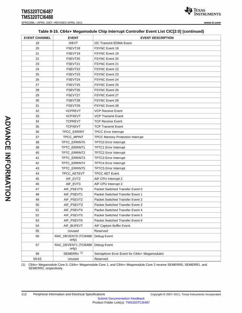
AD
VA
NC
E IN
FO
RM
AT
ION
TMS320TCI6487TMS320TCI6488SPRS358L–APRIL 2007–REVISED APRIL 2011 www.ti.com
Table 8-15. C64x+ Megamodule Chip Interrupt Controller Event List CIC[2:0] (continued)
EVENT CHANNEL EVENT EVENT DESCRIPTION
19 IXEVT I2C Transmit EDMA Event
20 FSEVT18 FSYNC Event 18
21 FSEVT19 FSYNC Event 19
22 FSEVT20 FSYNC Event 20
23 FSEVT21 FSYNC Event 21
24 FSEVT22 FSYNC Event 22
25 FSEVT23 FSYNC Event 23
26 FSEVT24 FSYNC Event 24
27 FSEVT25 FSYNC Event 25
28 FSEVT26 FSYNC Event 26
29 FSEVT27 FSYNC Event 27
30 FSEVT28 FSYNC Event 28
31 FSEVT29 FSYNC Event 28
32 VCPREVT VCP Receive Event
33 VCPXEVT VCP Transmit Event
34 TCPREVT TCP Receive Event
35 TCPXEVT TCP Transmit Event
36 TPCC_ERRINT TPCC Error Interrupt
37 TPCC_MPINT TPCC Memory Protection Interrupt
38 TPTC_ERRINT0 TPTC0 Error Interrupt
39 TPTC_ERRINT1 TPTC1 Error Interrupt
40 TPTC_ERRINT2 TPTC2 Error Interrupt
41 TPTC_ERRINT3 TPTC3 Error Interrupt
42 TPTC_ERRINT4 TPTC4 Error Interrupt
43 TPTC_ERRINT5 TPTC5 Error Interrupt
44 TPCC_AETEVT TPCC AET Event
45 AIF_EVT2 AIF CPU Interrupt 2
46 AIF_EVT3 AIF CPU Interrupt 2
47 AIF_PSEVT0 Packet Switched Transfer Event 0
48 AIF_PSEVT1 Packet Switched Transfer Event 1
49 AIF_PSEVT2 Packet Switched Transfer Event 2
50 AIF_PSEVT3 Packet Switched Transfer Event 3
51 AIF_PSEVT4 Packet Switched Transfer Event 4
52 AIF_PSEVT5 Packet Switched Transfer Event 5
53 AIF_PSEVT6 Packet Switched Transfer Event 6
54 AIF_BUFEVT AIF Capture Buffer Event.
55 Unused Reserved
56 RAC_DEVENT0 (TCI6488 Debug Eventonly)
57 RAC_DEVENT1 (TCI6488 Debug Eventonly)
58 SEMERRn (1) Semaphore Error Event for C64x+ Megamodulen
59-63 Unused Reserved
(1) C64x+ Megamodule Core 0, C64x+ Megamodule Core 1, and C64x+ Megamodule Core 2 receive SEMERR0, SEMERR1, andSEMERR2, respectively.
112 Peripheral Information and Electrical Specifications Copyright © 2007–2011, Texas Instruments Incorporated
Submit Documentation FeedbackProduct Folder Link(s): TMS320TCI6487

AD
VA
NC
E I
NF
OR
MA
TIO
N
TMS320TCI6487TMS320TCI6488
www.ti.com SPRS358L–APRIL 2007–REVISED APRIL 2011
Another system event selector is present to route events to the TPCC. Most system events routed throughthe event controller to the TPCC are CPU events that do not normally require DMA servicing, but may beused to trigger a statistics capture. Several events are routed through the event controller that may beused to trigger a DMA transaction in normal operation, but the programmer must make a resource tradeoffto use these events. Table 8-16 lists all of the events routed through the TPCCs system event controller.
Copyright © 2007–2011, Texas Instruments Incorporated Peripheral Information and Electrical Specifications 113Submit Documentation Feedback
Product Folder Link(s): TMS320TCI6487
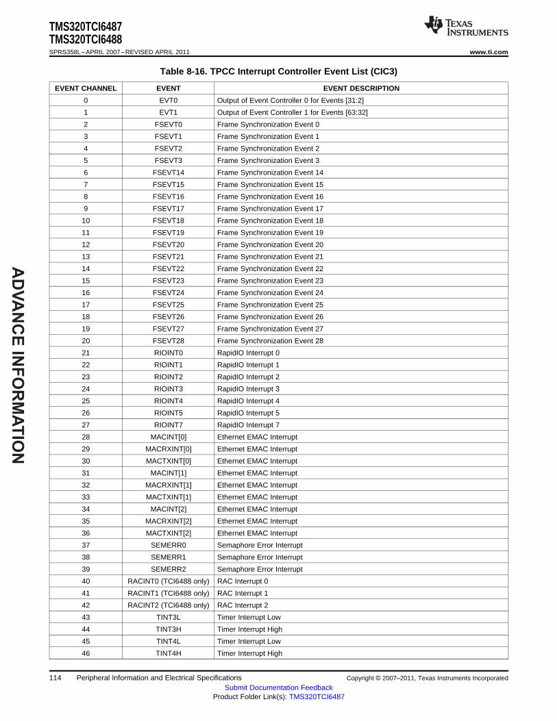
AD
VA
NC
E IN
FO
RM
AT
ION
TMS320TCI6487TMS320TCI6488SPRS358L–APRIL 2007–REVISED APRIL 2011 www.ti.com
Table 8-16. TPCC Interrupt Controller Event List (CIC3)
EVENT CHANNEL EVENT EVENT DESCRIPTION
0 EVT0 Output of Event Controller 0 for Events [31:2]
1 EVT1 Output of Event Controller 1 for Events [63:32]
2 FSEVT0 Frame Synchronization Event 0
3 FSEVT1 Frame Synchronization Event 1
4 FSEVT2 Frame Synchronization Event 2
5 FSEVT3 Frame Synchronization Event 3
6 FSEVT14 Frame Synchronization Event 14
7 FSEVT15 Frame Synchronization Event 15
8 FSEVT16 Frame Synchronization Event 16
9 FSEVT17 Frame Synchronization Event 17
10 FSEVT18 Frame Synchronization Event 18
11 FSEVT19 Frame Synchronization Event 19
12 FSEVT20 Frame Synchronization Event 20
13 FSEVT21 Frame Synchronization Event 21
14 FSEVT22 Frame Synchronization Event 22
15 FSEVT23 Frame Synchronization Event 23
16 FSEVT24 Frame Synchronization Event 24
17 FSEVT25 Frame Synchronization Event 25
18 FSEVT26 Frame Synchronization Event 26
19 FSEVT27 Frame Synchronization Event 27
20 FSEVT28 Frame Synchronization Event 28
21 RIOINT0 RapidIO Interrupt 0
22 RIOINT1 RapidIO Interrupt 1
23 RIOINT2 RapidIO Interrupt 2
24 RIOINT3 RapidIO Interrupt 3
25 RIOINT4 RapidIO Interrupt 4
26 RIOINT5 RapidIO Interrupt 5
27 RIOINT7 RapidIO Interrupt 7
28 MACINT[0] Ethernet EMAC Interrupt
29 MACRXINT[0] Ethernet EMAC Interrupt
30 MACTXINT[0] Ethernet EMAC Interrupt
31 MACINT[1] Ethernet EMAC Interrupt
32 MACRXINT[1] Ethernet EMAC Interrupt
33 MACTXINT[1] Ethernet EMAC Interrupt
34 MACINT[2] Ethernet EMAC Interrupt
35 MACRXINT[2] Ethernet EMAC Interrupt
36 MACTXINT[2] Ethernet EMAC Interrupt
37 SEMERR0 Semaphore Error Interrupt
38 SEMERR1 Semaphore Error Interrupt
39 SEMERR2 Semaphore Error Interrupt
40 RACINT0 (TCI6488 only) RAC Interrupt 0
41 RACINT1 (TCI6488 only) RAC Interrupt 1
42 RACINT2 (TCI6488 only) RAC Interrupt 2
43 TINT3L Timer Interrupt Low
44 TINT3H Timer Interrupt High
45 TINT4L Timer Interrupt Low
46 TINT4H Timer Interrupt High
114 Peripheral Information and Electrical Specifications Copyright © 2007–2011, Texas Instruments Incorporated
Submit Documentation FeedbackProduct Folder Link(s): TMS320TCI6487

AD
VA
NC
E I
NF
OR
MA
TIO
N
TMS320TCI6487TMS320TCI6488
www.ti.com SPRS358L–APRIL 2007–REVISED APRIL 2011
Table 8-16. TPCC Interrupt Controller Event List (CIC3) (continued)
EVENT CHANNEL EVENT EVENT DESCRIPTION
47 TINT5L Timer Interrupt Low
48 TINT5H Timer Interrupt High
49 AIF_BUFEVT AIF Capture Buffer Event
50 FSEVT29 Frame Synchronization Event 29
51 RAC_DEVENT0 (TCI6488 Debug Eventonly)
52 RAC_DEVENT1 (TCI6488 Debug Eventonly)
53 GPINT0 GPIO Event
54 GPINT1 GPIO Event
55 GPINT2 GPIO Event
56 GPINT3 GPIO Event
57 GPINT4 GPIO Event
58 CIC0_EVT14 CIC_EVT_o[14] from Chip Interrupt Controller[0]
59 CIC0_EVT15 CIC_EVT_o[15] from Chip Interrupt Controller[0]
60 CIC1_EVT14 CIC_EVT_o[14] from Chip Interrupt Controller[1]
61 CIC1_EVT15 CIC_EVT_o[15] from Chip Interrupt Controller[1]
62 CIC2_EVT14 CIC_EVT_o[14] from Chip Interrupt Controller[2]
63 CIC2_EVT15 CIC_EVT_o[15] from Chip Interrupt Controller[2]
Copyright © 2007–2011, Texas Instruments Incorporated Peripheral Information and Electrical Specifications 115Submit Documentation Feedback
Product Folder Link(s): TMS320TCI6487

AD
VA
NC
E IN
FO
RM
AT
ION
12
NMI
TMS320TCI6487TMS320TCI6488SPRS358L–APRIL 2007–REVISED APRIL 2011 www.ti.com
8.6.3 External Interrupts Electrical Data/Timing
Table 8-17. Timing Requirements for External Interrupts (1)
(see Figure 8-5)
NO. PARAMETERS MIN MAX UNIT
1 tw(NMIL) Width of the NMI interrupt pulse low 6P ns
2 tw(NMIH) Width of the NMI interrupt pulse high 6P ns
(1) P = 1/CPU clock frequency, in ns. For example, when running parts at 1000 MHz, use P = 1 ns.
Figure 8-5. NMI Interrupt Timing
116 Peripheral Information and Electrical Specifications Copyright © 2007–2011, Texas Instruments Incorporated
Submit Documentation FeedbackProduct Folder Link(s): TMS320TCI6487
AD
VA
NC
E I
NF
OR
MA
TIO
N
TMS320TCI6487TMS320TCI6488
www.ti.com SPRS358L–APRIL 2007–REVISED APRIL 2011
8.7 Reset Controller
The reset controller detects the different type of resets supported on the device and manages thedistribution of those resets throughout the device.
The TCI6487/8 device has several types of resets: power-on reset, warm reset, system reset, and CPUreset. Table 8-18 explains further the types of reset, the reset initiator, and the effects of each reset on thechip.
Table 8-18. Reset Types
TYPE INITIATOR EFFECT(S)
Power-on Reset POR pin Resets the entire chip including the test and emulation logic.
Warm Reset XWRST pin Resets everything except for the test and emulation logic PLL2, AIF, and FSYNC. Emulationstays alive during warm reset.
System Reset Emulator A system reset maintains memory contents and does not reset the test and emulationSerial RapidIO circuitry. The device configuration pins are also not re-latched and the state of the
peripherals (enabled/disabled) are also not affected.
CPU Local Reset Watchdog Timer CPU local reset.
8.7.1 Power-on Reset (POR Pin)
Power-on Reset is a special reset needed when powering on the DSP. The device is globally resetthrough the assertion of the active-low Power-on Reset (POR) input. The power-on reset is intended to beasserted to the device while the system power supplies are ramped.
For power-on reset, the main PLL Controller comes up in bypass and the PLL is not enabled. Other resetsdo not affect the state of the PLL or the dividers in the PLL Controller. For the secondary PLL Controller,this is different as the PLL is enabled and clocking always when POR is not asserted.
The following sequence must be followed during a power-on reset.
1. Wait for all power supplies to reach normal operating conditions while keeping the POR pin asserted(driven low). While POR is asserted, all pins except RESETSTAT will be set to high-impedance. Afterthe POR pin is de-asserted (driven high), all Z group pins, low group pins, and high group pins are setto their reset state and will remain at their reset state until otherwise configured by their respectiveperipheral. All peripherals that are power managed, are disabled after a Power-on Reset and must beenabled through the Device State Control registers (for more details, see Section 3.2, PeripheralSelection After Device Reset.
2. Clocks are reset, and they are propagated throughout the chip to reset any logic that was using resetsynchronously. All logic is now reset and RESETSTAT will be driven low indicating that the device is inreset.
3. POR must be held active until all supplies on the board are stable then for at least an additional 100μs.
4. The POR pin can now be de-asserted. Reset sampled pin values are latched at this point. PLL2 istaken out of reset and begins its locking sequence, and all power-on device initialization also begins.
5. After device initialization is complete, the RESETSTAT pin is de-asserted (driven high). By this time,PLL2 has already completed its locking sequence and is outputting a valid clock. The system clocks ofboth PLL controllers are allowed to finish their current cycles and then paused for 10 cycles of theirrespective system reference clocks. After the pause, the system clocks are restarted at their defaultdivide by settings.
6. The device is now out of reset and device execution begins as dictated by the selected boot mode.
Copyright © 2007–2011, Texas Instruments Incorporated Peripheral Information and Electrical Specifications 117Submit Documentation Feedback
Product Folder Link(s): TMS320TCI6487

AD
VA
NC
E IN
FO
RM
AT
ION
TMS320TCI6487TMS320TCI6488SPRS358L–APRIL 2007–REVISED APRIL 2011 www.ti.com
8.7.2 Warm Reset
A warm reset will reset everything on the chip except the AIF, FSYNC, PLLs, PLL Controllers, test, andemulation logic. POR should also remain de-asserted during this time.
1. XWRST pin is pulled active low for a minimum of 24 CLKIN1 cycles. The reset signals flow to themodules reset by warm reset and sends a tri-state signal to most the I/O pads, to prevent off chipcontention.
2. Once all logic is reset, RESETSTAT is driven active to denote that the device is in reset.
3. XWRST pin can now be released. A minimal device initialization begins to occur. Note thatconfiguration pins are not re-latched and clocking is unaffected within the device.
4. After device initialization is complete, the RESETSTAT pin is de-asserted (driven high).
During warm reset, the DDR2 SDRAM memory content can be retained if the user places the DDR2SDRAM in self-refresh mode before invoking the warm reset; however, warm reset will reset the DDR2EMIF registers. The software needs to re-program all DDR2 EMIF registers to correct values after warmreset.
8.7.3 System Reset
System reset is initiated by the emulator or by the RapidIO module. It is triggered by clicking on theDebug → Advanced Resets → System Reset menu in Code Composer Studio using the emulator.System reset is also triggered by RIOINT[6], which is connected to the reset controller. It is considered asoft reset, meaning memory contents are maintained, it does not affect the clock logic, or the powercontrol logic of the peripherals.
1. The RESETSTAT pin goes low to indicate an internal reset is being generated. The reset is allowed topropagate through the system. Internal system clocks are not affected. PLLs also remain locked.
2. The boot sequence is started after the system clocks are restarted. Since the configuration pins(including the BOOTMODE[3:0] pins) are not latched with a System Reset, the previous values, asshown in the DEVSTAT register, are used to select the boot mode.
8.7.4 CPU Reset
(Timer 64 3, 4, and 5) can provide a local CPU reset if they are setup in watchdog mode. Timer64 3, 4,and 5 are allowed to reset C64x+ Megamodule Core 0, C64x+ Megamodule Core 1, and C64x+Megamodule Core 2, respectively.
8.7.5 Reset Priority
If any of the above reset sources occur simultaneously, the PLLCTRL only processes the highest priorityreset request. The reset request priorities are as follows (high to low):• Power-on Reset• Warm Reset• System Reset• CPU Reset
118 Peripheral Information and Electrical Specifications Copyright © 2007–2011, Texas Instruments Incorporated
Submit Documentation FeedbackProduct Folder Link(s): TMS320TCI6487

AD
VA
NC
E I
NF
OR
MA
TIO
N
TMS320TCI6487TMS320TCI6488
www.ti.com SPRS358L–APRIL 2007–REVISED APRIL 2011
8.7.6 Reset Controller Register
The reset type status (RSTYPE) register (029A 00E4) is the only register for the reset controller. Thisregister falls in the same memory range as the PLL1 controller registers [029A 0000 - 029A 01FF] (seeTable 8-19).
8.7.6.1 Reset Type Status Register Description
The reset type status (RSTYPE) register latches the cause of the last reset. If multiple reset sources occursimultaneously, this register latches the highest priority reset source. The reset type status register isshown in Figure 8-6 and described in Table 8-19.
31 16
Reserved
R-0
15 4 3 2 1 0
Reserved SRST Rsvd WRST POR
R-0 R-0 R-0 R-0 R-0
LEGEND: R/W = Read/Write; R = Read only; -n = value after reset
Figure 8-6. Reset Type Status Register (RSTYPE) [Hex Address: 029A 00E4]
Table 8-19. Reset Type Status Register (RSTYPE) Field Descriptions
BIT FIELD VALUE DESCRIPTION
31:4 Reserved Reserved. The reserved bit location is always read as 0. A value written to this field has not effect.
3 SRST System Reset.
0 System Reset was not the last reset to occur.
1 System Reset was the last reset to occur.
1 WRST Warm Reset.
0 Warm Reset was not the last reset to occur.
1 Warm Reset was the last reset to occur.
2 Reserved Reserved. The reserved bit location is always read as 0. A value written to this field has not effect.
0 POR Power-on Reset.
0 Power-on Reset was not the last reset to occur.
1 Power-on Reset was the last reset to occur.
Copyright © 2007–2011, Texas Instruments Incorporated Peripheral Information and Electrical Specifications 119Submit Documentation Feedback
Product Folder Link(s): TMS320TCI6487

AD
VA
NC
E IN
FO
RM
AT
ION
8
3
7
1
2
POR
XWRST
RESETSTAT
Boot and DeviceConfiguration Pins
TMS320TCI6487TMS320TCI6488SPRS358L–APRIL 2007–REVISED APRIL 2011 www.ti.com
8.7.7 Reset Electrical Data/Timing
Table 8-20. Timing Requirements for Reset (1) (2)
(see Figure 8-7 and Figure 8-8)
NO. MIN MAX UNIT
1 th(SUPPLY-POR) Hold Time, POR low after supplies stable and input clocks valid 100 μs
2 tsu(XWRSTH-PORH) Setup Time, XWRSTx high to POR high 100 μs
4 tw(XWRST) Pulse Duration, XWRST low 24C ns
7 ts(BOOT) Setup time, boot mode and configuration pins valid before POR 12C nsor XWRST high
8 th(BOOT) Hold time, bootmode and configuration pins valid after POR or 12C nsXWRST high
(1) If CORECLKSEL = 0, C = 1/SYSCLK(N|P) frequency, in ns.(2) If CORECLKSEL = 1, C = 1/ALTCORECLK(N|P) frequency, in ns.
Table 8-21. Switching Characteristics Over Recommended Operating Conditions During Reset (1)
(see Figure 8-7 and Figure 8-8)
NO. MIN MAX UNIT
3 td(PORH-RSTATH) Delay Time, POR high to RESETSTAT high 21000C ns
5 td(XWRSTH-RSTATH) Delay Time, XWRST high to RESETSTAT high 35C ns
(1) C = 1/CPU frequency, in ns.
Table 8-22. Switching Characteristics Over Recommended Operating Conditions for Warm Reset(see Figure 8-9)
NO. MIN MAX UNIT
9 tsu(PORH-XWRSTL) Setup time, POR high to XWRST low 1.34 ms
Figure 8-7. Power-On Reset Timing
120 Peripheral Information and Electrical Specifications Copyright © 2007–2011, Texas Instruments Incorporated
Submit Documentation FeedbackProduct Folder Link(s): TMS320TCI6487
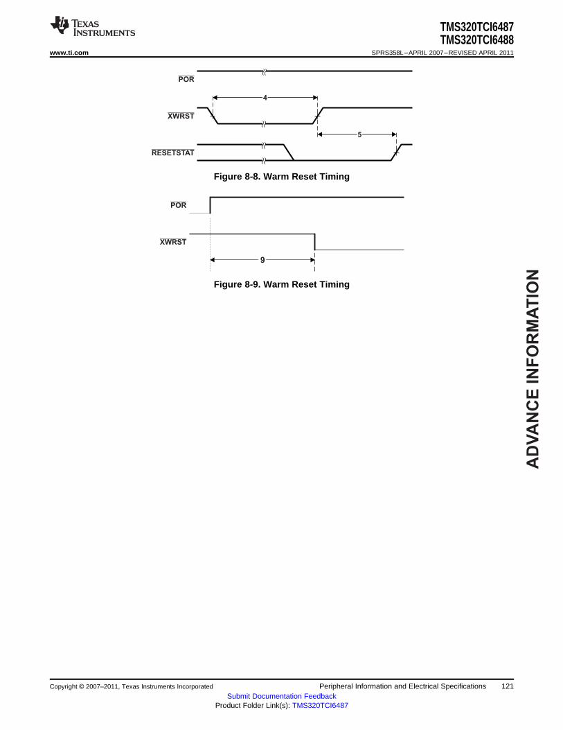
AD
VA
NC
E I
NF
OR
MA
TIO
N
4
5
POR
XWRST
RESETSTAT
POR
XWRST
9
TMS320TCI6487TMS320TCI6488
www.ti.com SPRS358L–APRIL 2007–REVISED APRIL 2011
Figure 8-8. Warm Reset Timing
Figure 8-9. Warm Reset Timing
Copyright © 2007–2011, Texas Instruments Incorporated Peripheral Information and Electrical Specifications 121Submit Documentation Feedback
Product Folder Link(s): TMS320TCI6487

AD
VA
NC
E IN
FO
RM
AT
ION
../1xM
Main PLL
AIF SERDES 0
x12.5, 10, 4
AIF SERDES 1
x12.5, 10, 4
Main.PLL Controller
../2
../n
To L2 and L2 PDCTL
C64x+ MegamoduleCore 0
C64x+ MegamoduleCore 1
C64x+ MegamoduleCore 2
To Trace
../4
../3
../6
../m
../20
RAC_CLK(A)
CHIP_CLK3
CHIP_CLK6
McBSP_CLKS
EMIF_PTV
To switch fabricperipherals,accelerators
SYS_CLK_(PIN)
ALT_CORE_CLK_(PIN)
CORE_CLK_SEL
AVDD118
/20
0
1
TMS320TCI6487TMS320TCI6488SPRS358L–APRIL 2007–REVISED APRIL 2011 www.ti.com
8.8 PLL1 and PLL1 Controller
This section provides a description of the PLL1 controller registers. For details on the operation of the PLLcontroller module, see the TMS320TCI6487/88 DSP Software-Programmable Phase-Locked Loop (PLL)Controller User's Guide (literature number SPRUEF1).
Note: The PLL1 controller registers can only be accessed using the CPU or the emulator.
Not all of the registers documented in the TMS320TCI6487/88 DSP Software-ProgrammablePhase-Locked Loop (PLL) Controller User's Guide (literature number SPRUEF1) are supported on theTCI6487/8 device. Only those registers documented in this section are supported. Furthermore, only thebits within the registers described here are supported. You should not write to any reserved memorylocation or change the value of reserved bits.
The Main and DDR PLLs are controlled by standard PLL Controller peripherals. The PLL Controllersmanage the clock ratios, alignment, and gating for the system clocks to the chip. Figure 8-10 includes ablock diagram of the PLL Controller, and the two subsequent sections define the clocks and PLLController parameters for each of the two standard PLLs.
The PLL controller logic is responsible for controlling all modes of the PLL through software, in termsmultiply factor within the PLL and post-division for each of the chip-level clocks from the PLL output. ThePLL controller also controls reset propagation through the chip, clock alignment, and test points. The PLLcontroller monitors the PLL status and provides an output signal indicating when the PLL is locked.
A. TCI6488 only.
Figure 8-10. PLL Controller Diagram
122 Peripheral Information and Electrical Specifications Copyright © 2007–2011, Texas Instruments Incorporated
Submit Documentation FeedbackProduct Folder Link(s): TMS320TCI6487
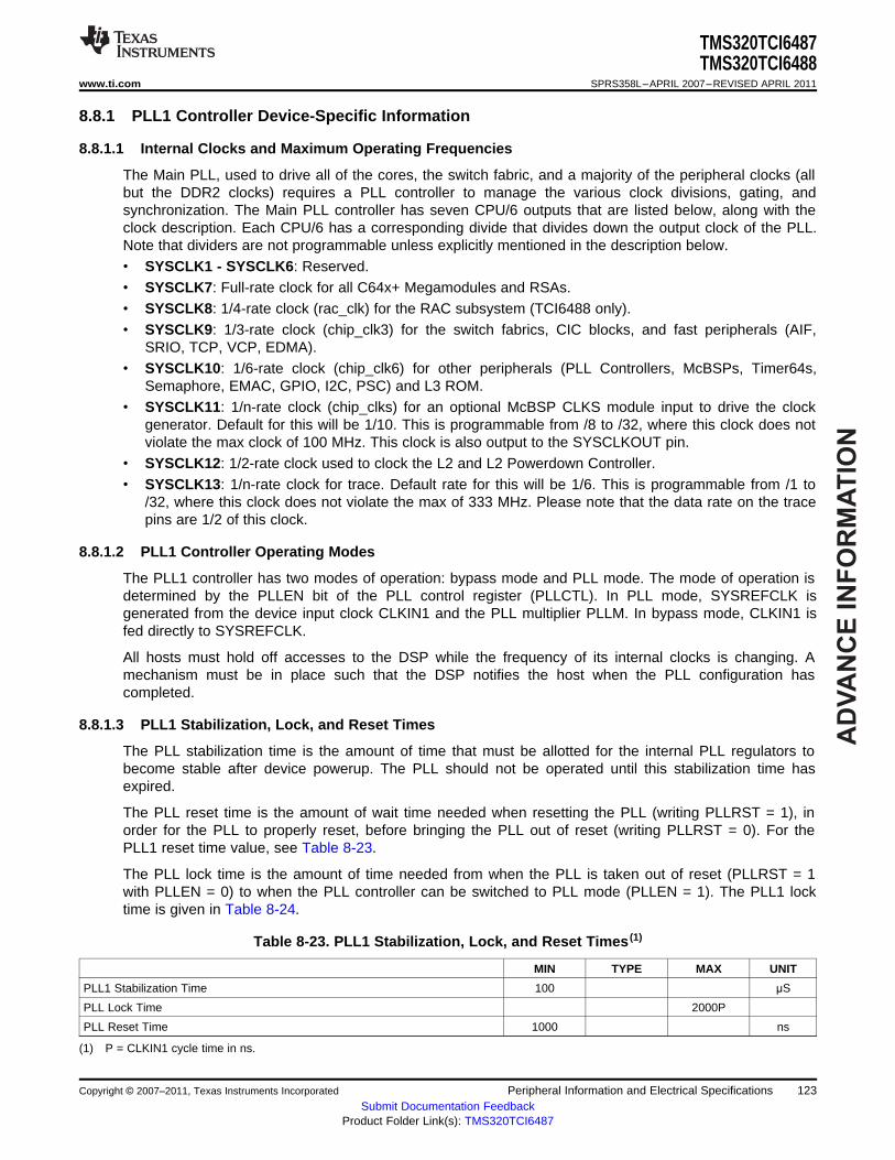
AD
VA
NC
E I
NF
OR
MA
TIO
N
TMS320TCI6487TMS320TCI6488
www.ti.com SPRS358L–APRIL 2007–REVISED APRIL 2011
8.8.1 PLL1 Controller Device-Specific Information
8.8.1.1 Internal Clocks and Maximum Operating Frequencies
The Main PLL, used to drive all of the cores, the switch fabric, and a majority of the peripheral clocks (allbut the DDR2 clocks) requires a PLL controller to manage the various clock divisions, gating, andsynchronization. The Main PLL controller has seven CPU/6 outputs that are listed below, along with theclock description. Each CPU/6 has a corresponding divide that divides down the output clock of the PLL.Note that dividers are not programmable unless explicitly mentioned in the description below.• SYSCLK1 - SYSCLK6: Reserved.• SYSCLK7: Full-rate clock for all C64x+ Megamodules and RSAs.• SYSCLK8: 1/4-rate clock (rac_clk) for the RAC subsystem (TCI6488 only).• SYSCLK9: 1/3-rate clock (chip_clk3) for the switch fabrics, CIC blocks, and fast peripherals (AIF,
SRIO, TCP, VCP, EDMA).• SYSCLK10: 1/6-rate clock (chip_clk6) for other peripherals (PLL Controllers, McBSPs, Timer64s,
Semaphore, EMAC, GPIO, I2C, PSC) and L3 ROM.• SYSCLK11: 1/n-rate clock (chip_clks) for an optional McBSP CLKS module input to drive the clock
generator. Default for this will be 1/10. This is programmable from /8 to /32, where this clock does notviolate the max clock of 100 MHz. This clock is also output to the SYSCLKOUT pin.
• SYSCLK12: 1/2-rate clock used to clock the L2 and L2 Powerdown Controller.• SYSCLK13: 1/n-rate clock for trace. Default rate for this will be 1/6. This is programmable from /1 to
/32, where this clock does not violate the max of 333 MHz. Please note that the data rate on the tracepins are 1/2 of this clock.
8.8.1.2 PLL1 Controller Operating Modes
The PLL1 controller has two modes of operation: bypass mode and PLL mode. The mode of operation isdetermined by the PLLEN bit of the PLL control register (PLLCTL). In PLL mode, SYSREFCLK isgenerated from the device input clock CLKIN1 and the PLL multiplier PLLM. In bypass mode, CLKIN1 isfed directly to SYSREFCLK.
All hosts must hold off accesses to the DSP while the frequency of its internal clocks is changing. Amechanism must be in place such that the DSP notifies the host when the PLL configuration hascompleted.
8.8.1.3 PLL1 Stabilization, Lock, and Reset Times
The PLL stabilization time is the amount of time that must be allotted for the internal PLL regulators tobecome stable after device powerup. The PLL should not be operated until this stabilization time hasexpired.
The PLL reset time is the amount of wait time needed when resetting the PLL (writing PLLRST = 1), inorder for the PLL to properly reset, before bringing the PLL out of reset (writing PLLRST = 0). For thePLL1 reset time value, see Table 8-23.
The PLL lock time is the amount of time needed from when the PLL is taken out of reset (PLLRST = 1with PLLEN = 0) to when the PLL controller can be switched to PLL mode (PLLEN = 1). The PLL1 locktime is given in Table 8-24.
Table 8-23. PLL1 Stabilization, Lock, and Reset Times (1)
MIN TYPE MAX UNIT
PLL1 Stabilization Time 100 μS
PLL Lock Time 2000P
PLL Reset Time 1000 ns
(1) P = CLKIN1 cycle time in ns.
Copyright © 2007–2011, Texas Instruments Incorporated Peripheral Information and Electrical Specifications 123Submit Documentation Feedback
Product Folder Link(s): TMS320TCI6487
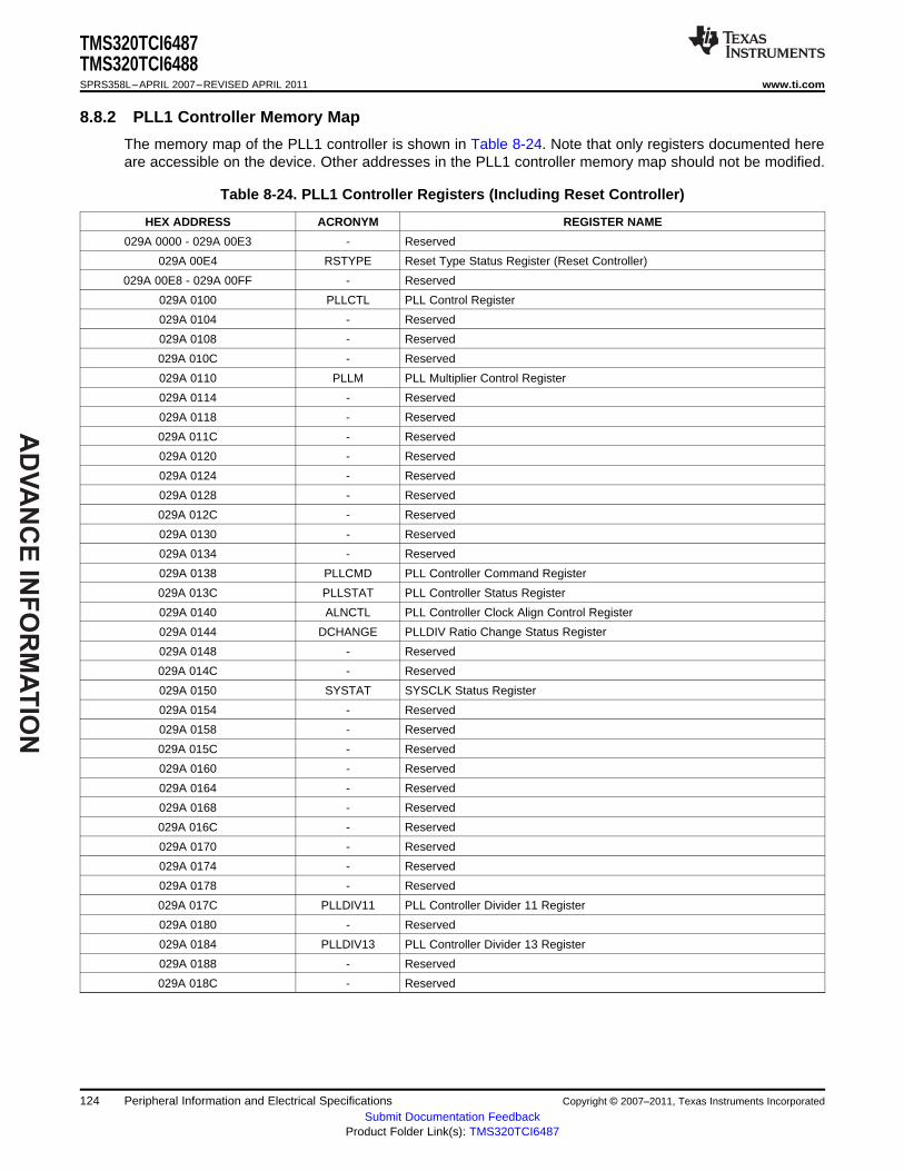
AD
VA
NC
E IN
FO
RM
AT
ION
TMS320TCI6487TMS320TCI6488SPRS358L–APRIL 2007–REVISED APRIL 2011 www.ti.com
8.8.2 PLL1 Controller Memory Map
The memory map of the PLL1 controller is shown in Table 8-24. Note that only registers documented hereare accessible on the device. Other addresses in the PLL1 controller memory map should not be modified.
Table 8-24. PLL1 Controller Registers (Including Reset Controller)
HEX ADDRESS ACRONYM REGISTER NAME
029A 0000 - 029A 00E3 - Reserved
029A 00E4 RSTYPE Reset Type Status Register (Reset Controller)
029A 00E8 - 029A 00FF - Reserved
029A 0100 PLLCTL PLL Control Register
029A 0104 - Reserved
029A 0108 - Reserved
029A 010C - Reserved
029A 0110 PLLM PLL Multiplier Control Register
029A 0114 - Reserved
029A 0118 - Reserved
029A 011C - Reserved
029A 0120 - Reserved
029A 0124 - Reserved
029A 0128 - Reserved
029A 012C - Reserved
029A 0130 - Reserved
029A 0134 - Reserved
029A 0138 PLLCMD PLL Controller Command Register
029A 013C PLLSTAT PLL Controller Status Register
029A 0140 ALNCTL PLL Controller Clock Align Control Register
029A 0144 DCHANGE PLLDIV Ratio Change Status Register
029A 0148 - Reserved
029A 014C - Reserved
029A 0150 SYSTAT SYSCLK Status Register
029A 0154 - Reserved
029A 0158 - Reserved
029A 015C - Reserved
029A 0160 - Reserved
029A 0164 - Reserved
029A 0168 - Reserved
029A 016C - Reserved
029A 0170 - Reserved
029A 0174 - Reserved
029A 0178 - Reserved
029A 017C PLLDIV11 PLL Controller Divider 11 Register
029A 0180 - Reserved
029A 0184 PLLDIV13 PLL Controller Divider 13 Register
029A 0188 - Reserved
029A 018C - Reserved
124 Peripheral Information and Electrical Specifications Copyright © 2007–2011, Texas Instruments Incorporated
Submit Documentation FeedbackProduct Folder Link(s): TMS320TCI6487

AD
VA
NC
E I
NF
OR
MA
TIO
N
TMS320TCI6487TMS320TCI6488
www.ti.com SPRS358L–APRIL 2007–REVISED APRIL 2011
8.8.3 PLL1 Controller Register Descriptions
This section provides a description of the PLL1 controller registers. For details on the operation of the PLLcontroller module, see the TMS320TCI6487/88 DSP Software-Programmable Phase-Locked Loop (PLL)Controller User's Guide (literature number SPRUEF1).
NOTE: The PLL1 controller registers can only be accessed using the CPU or the emulator.
Not all of the registers documented in the TMS320TCI6487/88 DSP Software-ProgrammablePhase-Locked Loop (PLL) Controller User's Guide (literature number SPRUEF1) are supported on theTCI6487/8 device. Only those registers documented in this section are supported. Furthermore, only thebits within the registers described here are supported. You should not write to any reserved memorylocation or change the value of reserved bits.
8.8.3.1 PLL1 Control Register
The PLL control register (PLLCTL) is shown in Figure 8-11 and described in Table 8-25.
31 16Reserved
R-0
15 8 7 6 5 4 3 2 1 0PLL
Reserved Rsvd Rsvd Reserved PLLRST Rsvd PLLENPWRDN
R-0 R/W-0 R-1 R/W-0 R/W-1 R-0 R/W-0 R/W-0
LEGEND: R/W = Read/Write; R = Read only; -n = value after reset
Figure 8-11. PLL1 Control Register (PLLCTL) [Hex Address: 029A 0100]
Table 8-25. PLL1 Control Register (PLLCTL) Field Descriptions
Bit Field Value Description
31:8 Reserved Reserved. The reserved bit location is always read as 0. A value written to this field has no effect.
7 Reserved Reserved. Writes to this register must keep this bit as 0.
6 Reserved Reserved. The reserved bit location is always read as 1. A value written to this field has no effect.
5:4 Reserved Reserved. Writes to this register must keep this bit as 0.
3 PLLRST PLL reset bit
0 PLL reset is released
1 PLL reset is asserted
2 Reserved Reserved. The reserved bit location is always read as 0. A value written to this field has no effect.
1 PLLPWRDN PLL power-down mode select bit
0 PLL is operational
1 PLL is placed in power-down state, i.e., all analog circuitry in the PLL is turned-off
0 PLLEN PLL enable bit
0 Bypass mode. PLL is bypassed. All the system clocks (SYSCLKn) are divided down directly frominput reference clock.
1 PLL mode. PLL is not bypassed. PLL output path is enabled. All the system clocks (SYSCLKn) aredivided down from PLL output.
Copyright © 2007–2011, Texas Instruments Incorporated Peripheral Information and Electrical Specifications 125Submit Documentation Feedback
Product Folder Link(s): TMS320TCI6487

AD
VA
NC
E IN
FO
RM
AT
ION
TMS320TCI6487TMS320TCI6488SPRS358L–APRIL 2007–REVISED APRIL 2011 www.ti.com
8.8.3.2 PLL Multiplier Control Register
The PLL multiplier control register (PLLM) is shown in Figure 8-12 and described in Table 8-26. The PLLMregister defines the input reference clock frequency multiplier.
31 16
Reserved
R-0
15 5 4 0
Reserved PLLM
R-0 R/W-0h
LEGEND: R/W = Read/Write; R = Read only; -n = value after reset
Figure 8-12. PLL Multiplier Control Register (PLLM) [Hex Address: 029A 0110]
Table 8-26. PLL Multiplier Control Register (PLLM) Field Descriptions (1)
Bit Field Value Description
31:5 Reserved 0 Reserved. The reserved bit location is always read as 0. A value written to this field has no effect.
4:0 PLLM PLL multiplier bits. Defines the input reference clock frequency multiplier.
0h Bypass
3h x4 multiplier rate
4h x5 multiplier rate
. .
. .
. .
1Eh x31 multiplier rate
1Fh x32 multiplier rate
(1) For more information, see Section 8.8.4.
126 Peripheral Information and Electrical Specifications Copyright © 2007–2011, Texas Instruments Incorporated
Submit Documentation FeedbackProduct Folder Link(s): TMS320TCI6487

AD
VA
NC
E I
NF
OR
MA
TIO
N
TMS320TCI6487TMS320TCI6488
www.ti.com SPRS358L–APRIL 2007–REVISED APRIL 2011
8.8.3.3 PLL Controller Divider 11 Register
The PLL controller divider 11 register (PLLDIV11) is shown in Figure 8-13 and described in Table 8-27.
31 16
Reserved
R-0
15 14 5 4 0
D11EN Reserved RATIO
R/W-1 R-0 R/W-3
LEGEND: R/W = Read/Write; R = Read only; -n = value after reset
Figure 8-13. PLL Controller Divider 11 Register (PLLDIV11) [Hex Address: 029A 017C]
Table 8-27. PLL Controller Divider 11 Register (PLLDIV11) Field Descriptions
Bit Field Value Description
31:16 Reserved 0 Reserved. The reserved bit location is always read as 0. A value written to this field has noeffect.
15 D11EN Divider 11 enable bit.
0 Divider 11 is disabled. No clock output.
1 Divider 11 is enabled.
14:5 Reserved 0 Reserved. The reserved bit location is always read as 0. A value written to this field has noeffect.
4:0 RATIO (1) 0-1Fh Divider ratio bits.
0h-4h Reserved, do not use.
7h-31h ÷8 to ÷ 32. Divide frequency by 8 to divide frequency by 32.
32h-1Fh Reserved, do not use.
(1) For more details, see SYSCLK11 description in Section 8.8.1.1.
Copyright © 2007–2011, Texas Instruments Incorporated Peripheral Information and Electrical Specifications 127Submit Documentation Feedback
Product Folder Link(s): TMS320TCI6487

AD
VA
NC
E IN
FO
RM
AT
ION
TMS320TCI6487TMS320TCI6488SPRS358L–APRIL 2007–REVISED APRIL 2011 www.ti.com
8.8.3.4 PLL Controller Divider 13 Register
The PLL controller divider 13 register (PLLDIV13) is shown in Figure 8-14 and described in Table 8-28.
31 16
Reserved
R-0
15 14 5 4 0
D13EN Reserved RATIO
R/W-1 R-0 R/W-3
LEGEND: R/W = Read/Write; R = Read only; -n = value after reset
Figure 8-14. PLL Controller Divider 13 Register (PLLDIV13) [Hex Address: 029A 0184]
Table 8-28. PLL Controller Divider 13 Register (PLLDIV13) Field Descriptions
Bit Field Value Description
31:16 Reserved 0 Reserved. The reserved bit location is always read as 0. A value written to this field has noeffect.
15 D13EN Divider 13 enable bit.
0 Divider 13 is disabled. No clock output.
1 Divider 13 is enabled.
14:5 Reserved 0 Reserved. The reserved bit location is always read as 0. A value written to this field has noeffect.
4:0 RATIO 0-1Fh Divider ratio bits.
0h-31h ÷1 to ÷32. Divide frequency by 1 to divide frequency by 32.
32h-1Fh Reserved, do not use.
128 Peripheral Information and Electrical Specifications Copyright © 2007–2011, Texas Instruments Incorporated
Submit Documentation FeedbackProduct Folder Link(s): TMS320TCI6487

AD
VA
NC
E I
NF
OR
MA
TIO
N
TMS320TCI6487TMS320TCI6488
www.ti.com SPRS358L–APRIL 2007–REVISED APRIL 2011
8.8.3.5 PLL Controller Command Register
The PLL controller command register (PLLCMD) contains the command bit for GO operation. PLLCMD isshown in Figure 8-15 and described in Table 8-29.
31 16
Reserved
R-0
15 2 1 0
Reserved Rsvd GOSET
R-0 R/W-0 R/W-0
LEGEND: R/W = Read/Write; R = Read only; -n = value after reset
Figure 8-15. PLL Controller Command Register (PLLCMD) [Hex Address: 029A 0138]
Table 8-29. PLL Controller Command Register (PLLCMD) Field Descriptions
Bit Field Value Description
31:2 Reserved 0 Reserved. The reserved bit location is always read as 0. A value written to this field has no effect.
1 Reserved Reserved. The reserved bit location is always read as 0. A value written to this field has no effect.
0 GOSET GO operation command for SYSCLK rate change and phase alignment. Before setting this bit to 1to initiate a GO operation, check the GOSTAT bit in the PLLSTAT register to ensure all previousGO operations have completed.
0 No effect. Write of 0 clears bit to 0.
1 Initiates GO operation. Write of 1 initiates GO operation. Once set, GOSET remains set but furtherwrites of 1 can initiate the GO operation.
Copyright © 2007–2011, Texas Instruments Incorporated Peripheral Information and Electrical Specifications 129Submit Documentation Feedback
Product Folder Link(s): TMS320TCI6487
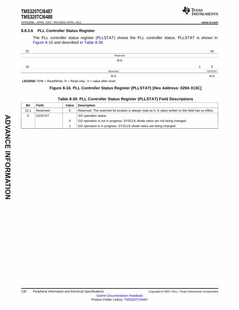
AD
VA
NC
E IN
FO
RM
AT
ION
TMS320TCI6487TMS320TCI6488SPRS358L–APRIL 2007–REVISED APRIL 2011 www.ti.com
8.8.3.6 PLL Controller Status Register
The PLL controller status register (PLLSTAT) shows the PLL controller status. PLLSTAT is shown inFigure 8-16 and described in Table 8-30.
31 16Reserved
R-0
15 1 0Reserved GOSTAT
R-0 R-0
LEGEND: R/W = Read/Write; R = Read only; -n = value after reset
Figure 8-16. PLL Controller Status Register (PLLSTAT) [Hex Address: 029A 013C]
Table 8-30. PLL Controller Status Register (PLLSTAT) Field Descriptions
Bit Field Value Description
31:1 Reserved 0 Reserved. The reserved bit location is always read as 0. A value written to this field has no effect.
0 GOSTAT GO operation status.
0 GO operation is not in progress. SYSCLK divide ratios are not being changed.
1 GO operation is in progress. SYSCLK divide ratios are being changed.
130 Peripheral Information and Electrical Specifications Copyright © 2007–2011, Texas Instruments Incorporated
Submit Documentation FeedbackProduct Folder Link(s): TMS320TCI6487
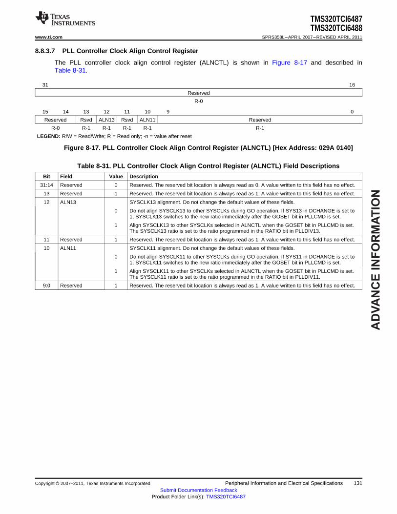
AD
VA
NC
E I
NF
OR
MA
TIO
N
TMS320TCI6487TMS320TCI6488
www.ti.com SPRS358L–APRIL 2007–REVISED APRIL 2011
8.8.3.7 PLL Controller Clock Align Control Register
The PLL controller clock align control register (ALNCTL) is shown in Figure 8-17 and described inTable 8-31.
31 16
Reserved
R-0
15 14 13 12 11 10 9 0
Reserved Rsvd ALN13 Rsvd ALN11 Reserved
R-0 R-1 R-1 R-1 R-1 R-1
LEGEND: R/W = Read/Write; R = Read only; -n = value after reset
Figure 8-17. PLL Controller Clock Align Control Register (ALNCTL) [Hex Address: 029A 0140]
Table 8-31. PLL Controller Clock Align Control Register (ALNCTL) Field Descriptions
Bit Field Value Description
31:14 Reserved 0 Reserved. The reserved bit location is always read as 0. A value written to this field has no effect.
13 Reserved 1 Reserved. The reserved bit location is always read as 1. A value written to this field has no effect.
12 ALN13 SYSCLK13 alignment. Do not change the default values of these fields.
0 Do not align SYSCLK13 to other SYSCLKs during GO operation. If SYS13 in DCHANGE is set to1, SYSCLK13 switches to the new ratio immediately after the GOSET bit in PLLCMD is set.
1 Align SYSCLK13 to other SYSCLKs selected in ALNCTL when the GOSET bit in PLLCMD is set.The SYSCLK13 ratio is set to the ratio programmed in the RATIO bit in PLLDIV13.
11 Reserved 1 Reserved. The reserved bit location is always read as 1. A value written to this field has no effect.
10 ALN11 SYSCLK11 alignment. Do not change the default values of these fields.
0 Do not align SYSCLK11 to other SYSCLKs during GO operation. If SYS11 in DCHANGE is set to1, SYSCLK11 switches to the new ratio immediately after the GOSET bit in PLLCMD is set.
1 Align SYSCLK11 to other SYSCLKs selected in ALNCTL when the GOSET bit in PLLCMD is set.The SYSCLK11 ratio is set to the ratio programmed in the RATIO bit in PLLDIV11.
9:0 Reserved 1 Reserved. The reserved bit location is always read as 1. A value written to this field has no effect.
Copyright © 2007–2011, Texas Instruments Incorporated Peripheral Information and Electrical Specifications 131Submit Documentation Feedback
Product Folder Link(s): TMS320TCI6487
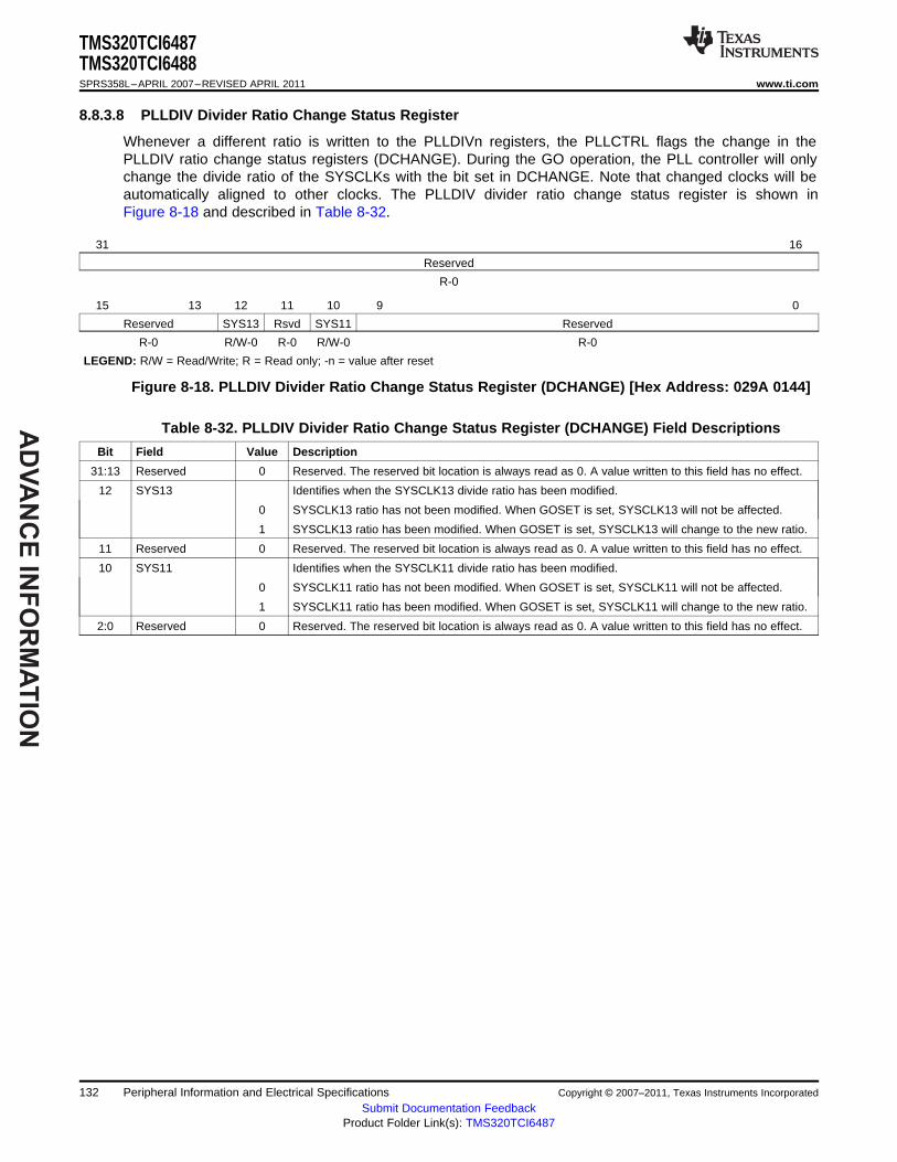
AD
VA
NC
E IN
FO
RM
AT
ION
TMS320TCI6487TMS320TCI6488SPRS358L–APRIL 2007–REVISED APRIL 2011 www.ti.com
8.8.3.8 PLLDIV Divider Ratio Change Status Register
Whenever a different ratio is written to the PLLDIVn registers, the PLLCTRL flags the change in thePLLDIV ratio change status registers (DCHANGE). During the GO operation, the PLL controller will onlychange the divide ratio of the SYSCLKs with the bit set in DCHANGE. Note that changed clocks will beautomatically aligned to other clocks. The PLLDIV divider ratio change status register is shown inFigure 8-18 and described in Table 8-32.
31 16
Reserved
R-0
15 13 12 11 10 9 0
Reserved SYS13 Rsvd SYS11 Reserved
R-0 R/W-0 R-0 R/W-0 R-0
LEGEND: R/W = Read/Write; R = Read only; -n = value after reset
Figure 8-18. PLLDIV Divider Ratio Change Status Register (DCHANGE) [Hex Address: 029A 0144]
Table 8-32. PLLDIV Divider Ratio Change Status Register (DCHANGE) Field Descriptions
Bit Field Value Description
31:13 Reserved 0 Reserved. The reserved bit location is always read as 0. A value written to this field has no effect.
12 SYS13 Identifies when the SYSCLK13 divide ratio has been modified.
0 SYSCLK13 ratio has not been modified. When GOSET is set, SYSCLK13 will not be affected.
1 SYSCLK13 ratio has been modified. When GOSET is set, SYSCLK13 will change to the new ratio.
11 Reserved 0 Reserved. The reserved bit location is always read as 0. A value written to this field has no effect.
10 SYS11 Identifies when the SYSCLK11 divide ratio has been modified.
0 SYSCLK11 ratio has not been modified. When GOSET is set, SYSCLK11 will not be affected.
1 SYSCLK11 ratio has been modified. When GOSET is set, SYSCLK11 will change to the new ratio.
2:0 Reserved 0 Reserved. The reserved bit location is always read as 0. A value written to this field has no effect.
132 Peripheral Information and Electrical Specifications Copyright © 2007–2011, Texas Instruments Incorporated
Submit Documentation FeedbackProduct Folder Link(s): TMS320TCI6487

AD
VA
NC
E I
NF
OR
MA
TIO
N
TMS320TCI6487TMS320TCI6488
www.ti.com SPRS358L–APRIL 2007–REVISED APRIL 2011
8.8.3.9 SYSCLK Status Register
The SYSCLK status register (SYSTAT) shows the status of the system clocks (SYSCLKn). SYSTAT isshown in Figure 8-19 and described in Table 8-33.
31 16
Reserved
R-1
15 13 12 11 10 9 8
Reserved SYS13ON SYS12ON SYS11ON SYS10ON SYS9ON
R-1 R-1 R-1 R-1 R-1 R-1
7 6 5 0
SYS8ON SYS7ON Reserved
R-1 R-1 R-1
LEGEND: R = Read only; -n = value after reset
Figure 8-19. SYSCLK Status Register (SYSTAT) [Hex Address: 029A 0150]
Table 8-33. SYSCLK Status Register (SYSTAT) Field Descriptions
Bit Field Value Description
31:13 Reserved 1 Reserved. The reserved bit location is always read as 1. A value written to this field has no effect.
12:6 SYSnON SYSCLKn on status.
0 SYSCLKn is gated.
1 SYSCLKn is on.
5:0 Reserved 1 Reserved. The reserved bit location is always read as 1. A value written to this field has no effect.
Copyright © 2007–2011, Texas Instruments Incorporated Peripheral Information and Electrical Specifications 133Submit Documentation Feedback
Product Folder Link(s): TMS320TCI6487
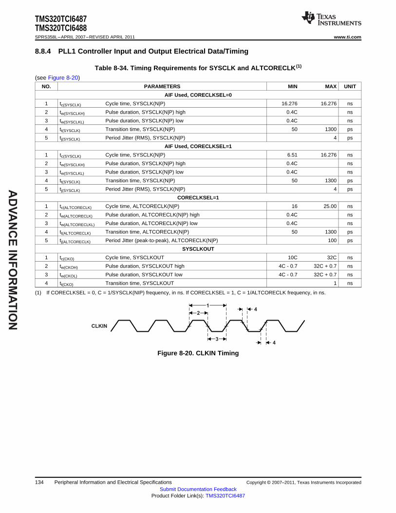
AD
VA
NC
E IN
FO
RM
AT
ION
2
1
3
4
4
CLKIN
TMS320TCI6487TMS320TCI6488SPRS358L–APRIL 2007–REVISED APRIL 2011 www.ti.com
8.8.4 PLL1 Controller Input and Output Electrical Data/Timing
Table 8-34. Timing Requirements for SYSCLK and ALTCORECLK (1)
(see Figure 8-20)
NO. PARAMETERS MIN MAX UNIT
AIF Used, CORECLKSEL=0
1 tc(SYSCLK) Cycle time, SYSCLK(N|P) 16.276 16.276 ns
2 tw(SYSCLKH) Pulse duration, SYSCLK(N|P) high 0.4C ns
3 tw(SYSCLKL) Pulse duration, SYSCLK(N|P) low 0.4C ns
4 tt(SYSCLK) Transition time, SYSCLK(N|P) 50 1300 ps
5 tj(SYSCLK) Period Jitter (RMS), SYSCLK(N|P) 4 ps
AIF Used, CORECLKSEL=1
1 tc(SYSCLK) Cycle time, SYSCLK(N|P) 6.51 16.276 ns
2 tw(SYSCLKH) Pulse duration, SYSCLK(N|P) high 0.4C ns
3 tw(SYSCLKL) Pulse duration, SYSCLK(N|P) low 0.4C ns
4 tt(SYSCLK) Transition time, SYSCLK(N|P) 50 1300 ps
5 tj(SYSCLK) Period Jitter (RMS), SYSCLK(N|P) 4 ps
CORECLKSEL=1
1 tc(ALTCORECLK) Cycle time, ALTCORECLK(N|P) 16 25.00 ns
2 tw(ALTCORECLK) Pulse duration, ALTCORECLK(N|P) high 0.4C ns
3 tw(ALTCORECLKL) Pulse duration, ALTCORECLK(N|P) low 0.4C ns
4 tt(ALTCORECLK) Transition time, ALTCORECLK(N|P) 50 1300 ps
5 tj(ALTCORECLK) Period Jitter (peak-to-peak), ALTCORECLK(N|P) 100 ps
SYSCLKOUT
1 tc(CKO) Cycle time, SYSCLKOUT 10C 32C ns
2 tw(CKOH) Pulse duration, SYSCLKOUT high 4C - 0.7 32C + 0.7 ns
3 tw(CKOL) Pulse duration, SYSCLKOUT low 4C - 0.7 32C + 0.7 ns
4 tt(CKO) Transition time, SYSCLKOUT 1 ns
(1) If CORECLKSEL = 0, C = 1/SYSCLK(NIP) frequency, in ns. If CORECLKSEL = 1, C = 1/ALTCORECLK frequency, in ns.
Figure 8-20. CLKIN Timing
134 Peripheral Information and Electrical Specifications Copyright © 2007–2011, Texas Instruments Incorporated
Submit Documentation FeedbackProduct Folder Link(s): TMS320TCI6487

AD
VA
NC
E I
NF
OR
MA
TIO
N
DDR.PLLAV
DD218
DDR.PLLController
PLLOUT
x10
DDR2
PHY÷ 2
TMS320TCI6487TMS320TCI6488
www.ti.com SPRS358L–APRIL 2007–REVISED APRIL 2011
8.9 PLL2 and PLL2 Controller
The secondary PLL controller generates interface clocks for the DDR2 memory controller. The CLKIN2input for PLL2 is DDRREFCLK. It is a differential clock input and is applied at the DDRREFCLKP andDDRREFCLKN pins. When coming out of power-on reset, PLL2 is enabled and initialized.
As shown in Figure 8-21, the PLL2 controller features a PLL multiplier controller. The PLL multiplier isfixed to a x10 multiplier rate.
PLL2 power is supplied externally via the PLL2 power supply (AVDD218). An external PLL filter circuit mustbe added to AVDD218 as shown in Figure 8-21. The 1.8-V supply for the EMI filter must be from the same1.8-V power plane supplying the I/O power-supply pin, DVDD18. TI requires EMI filter manufacturer Murata.For more information on the external PLL filter or the EMI filter, see the TMS320TCI6487/88 HardwareDesign Guide application report (literature number SPRAAG5).
All PLL external components (capacitors and the EMI filter) should be placed as close to the C64x+ DSPdevice as possible. For the best performance, TI requires that all the PLL external components be on asingle side of the board without jumpers, switches, or components other than the ones shown. Forreduced PLL jitter, maximize the spacing between switching signals and the PLL external components(capacitors and the EMI filter). The minimum CLKIN2 rise and fall times should also be observed.
Figure 8-21. PLL2 Block Diagram
8.9.1 PLL2 Controller Device-Specific Information
8.9.1.1 Internal Clocks and Maximum Operating Frequencies
As shown in Figure 8-21, the output of PLL2, PLLOUT, is divided by 2 and directly fed to the DDR2memory controller. This clock is used by the DDR2 memory controller to generate DDR2CLKOUT0[P/N]and DDR2CLKOUT1[P/N]. Note that, internally, the data bus interface of the DDR2 memory controller isclocked by SYSCLK2 and PLL1 controller.
Note that there is a minimum and maximum operating frequency for DDRREFCLK and PLLOUT. Theclock generator and PLL multiplier must not be configured to exceed any of these constraints. For the PLLclocks input and output frequency ranges, see Table 8-35. DDRREFCLK is a differential clock input toPLL2 and is applied at the DDRREFCLKP and DDRREFCLKN pins.
Table 8-35. PLL2 Clock Frequency Ranges
MIN MAX UNIT
DDRREFCLK (PLLEN = 1) 40 66.7 MHz
PLLOUT 400 667 MHz
DDR2CLKOUT0[P/N] and DDR2CLKOUT1[P/N] 200 333 MHz
Copyright © 2007–2011, Texas Instruments Incorporated Peripheral Information and Electrical Specifications 135Submit Documentation Feedback
Product Folder Link(s): TMS320TCI6487
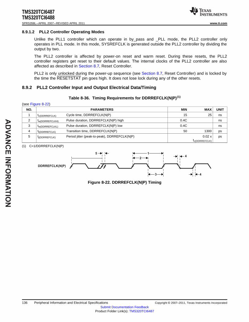
AD
VA
NC
E IN
FO
RM
AT
ION
2
1
3
4
4
DDRREFCLK(N|P)
5
TMS320TCI6487TMS320TCI6488SPRS358L–APRIL 2007–REVISED APRIL 2011 www.ti.com
8.9.1.2 PLL2 Controller Operating Modes
Unlike the PLL1 controller which can operate in by_pass and _PLL mode, the PLL2 controller onlyoperates in PLL mode. In this mode, SYSREFCLK is generated outside the PLL2 controller by dividing theoutput by two.
The PLL2 controller is affected by power-on reset and warm reset. During these resets, the PLL2controller registers get reset to their default values. The internal clocks of the PLL2 controller are alsoaffected as described in Section 8.7, Reset Controller.
PLL2 is only unlocked during the power-up sequence (see Section 8.7, Reset Controller) and is locked bythe time the RESETSTAT pin goes high. It does not lose lock during any of the other resets.
8.9.2 PLL2 Controller Input and Output Electrical Data/Timing
Table 8-36. Timing Requirements for DDRREFCLK(N|P) (1)
(see Figure 8-22)
NO. PARAMETERS MIN MAX UNIT
1 tc(DDRREFCLK) Cycle time, DDRREFCLK(N|P) 15 25 ns
2 tw(DDRREFCLKH) Pulse duration, DDRREFCLK(N|P) high 0.4C ns
3 tw(DDRREFCLKL) Pulse duration, DDRREFCLK(N|P) low 0.4C ns
4 tt(DDRREFCLK) Transition time, DDRREFCLK(N|P) 50 1300 ps
5 tj(DDRREFCLK) Period jitter (peak-to-peak), DDRREFCLK(N|P) 0.02 x pstc(DDRREFCLK)
(1) C=1/DDRREFCLK(N|P)
Figure 8-22. DDRREFCLK(N|P) Timing
136 Peripheral Information and Electrical Specifications Copyright © 2007–2011, Texas Instruments Incorporated
Submit Documentation FeedbackProduct Folder Link(s): TMS320TCI6487
AD
VA
NC
E I
NF
OR
MA
TIO
N
TMS320TCI6487TMS320TCI6488
www.ti.com SPRS358L–APRIL 2007–REVISED APRIL 2011
8.10 DDR2 Memory Controller
The 32-bit DDR2 Memory Controller bus of the TCI6487/8 device is used to interface to JESD79-2Bstandard-compliant DDR2 SDRAM devices. The DDR2 bus is designed to sustain a throughput of up to2.67 GBps at a 667-MHz data rate (333-MHz clock rate) as long as data requests are pending in theDDR2 Memory Controller.
The DDR2 external bus only interfaces to DDR2 SDRAM devices; it does not share the bus with any othertypes of peripherals.
8.10.1 DDR2 Memory Controller Device-Specific Information
The approach to specifying interface timing for the DDR2 memory bus is different than on other interfacessuch as McBSP. For these other interfaces the device timing was specified in terms of data manualspecifications and I/O buffer information specification (IBIS) models.
For the TCI6487/8 DDR2 memory bus, the approach is to specify compatible DDR2 devices and providethe printed circuit board (PCB) solution and guidelines directly to the user. Texas Instruments (TI) hasperformed the simulation and system characterization to ensure all DDR2 interface timings in this solutionare met. The complete DDR2 system solution is documented in the TMS320TCI6484/6487/6488 DDR2Implementation Guidelines application report (literature number SPRAAG6).
TI only supports designs that follow the board design guidelines outlined in the SPRAAG6application report.
The DDR2 memory controller on the TCI6487/8 device supports the following memory topologies:• 32-bit wide configuration interfacing to two 16-bit wide DDR2 SDRAM devices.• 16-bit wide configuration interfacing to a single 16-bit wide DDR2 SDRAM device.
A race condition may exist when certain masters write data to the DDR2 memory controller. For example,if master A passes a software message via a buffer in external memory and does not wait for indicationthat the write completes, when master B attempts to read the software message, then the master B readmay bypass the master A write and, thus, master B may read stale data and, therefore, receive anincorrect message.
Some master peripherals (e.g., EDMA3 transfer controllers) will always wait for the write to completebefore signaling an interrupt to the system, thus avoiding this race condition. For masters that do not havehardware specification of write-read ordering, it may be necessary to specify data ordering via software.
If master A does not wait for an indication that a write is complete, it must perform the followingworkaround:
1. Perform the required write.
2. Perform a dummy write to the DDR2 memory controller module ID and revision register.
3. Perform a dummy read to the DDR2 memory controller module ID and revision register.
4. Indicate to master B that the data is ready to be read after completion of the read in step 3. Thecompletion of the read in step 3 ensures that the previous write was done.
Copyright © 2007–2011, Texas Instruments Incorporated Peripheral Information and Electrical Specifications 137Submit Documentation Feedback
Product Folder Link(s): TMS320TCI6487

AD
VA
NC
E IN
FO
RM
AT
ION
TMS320TCI6487TMS320TCI6488SPRS358L–APRIL 2007–REVISED APRIL 2011 www.ti.com
8.10.2 DDR2 Memory Controller Peripheral Register Description(s)
The memory map of the DDR2 controller is shown in Table 8-37.
Table 8-37. DDR2 Memory Controller Registers
HEX ADDRESS ACRONYM REGISTER NAME
7000 0000 MIDR DDR2 Memory Controller Module and Revision Register
7000 0004 DMCSTAT DDR2 Memory Controller Status Register
7000 0008 SDCFG DDR2 Memory Controller SDRAM Configuration Register
7000 000C SDRFC DDR2 Memory Controller SDRAM Refresh Control Register
7000 0010 SDTIM1 DDR2 Memory Controller SDRAM Timing 1 Register
7000 0014 SDTIM2 DDR2 Memory Controller SDRAM Timing 2 Register
7000 0018 - Reserved
7000 0020 BPRIO DDR2 Memory Controller Burst Priority Register
7000 0024 - 7000 004C - Reserved
7000 0050 - 7000 0078 - Reserved
7000 007C - 7000 00BC - Reserved
7000 00C0 - 7000 00E0 - Reserved
7000 00E4 DMCCTL DDR2 Memory Controller Control Register
7000 00E8 - 7000 00EC - Reserved
7000 00F0 DDR2IO Control RegisterDDR2 ODT control register is at 0x7000 00F0Bits 1:0 are the ODT status, these bits are Read/Write
00 no termination01 half termination11 full termination
Bits 31:2 are Reserved
7000 00F4 - 7000 00FC - Reserved
7000 0100 - 7FFF FFFF - Reserved
138 Peripheral Information and Electrical Specifications Copyright © 2007–2011, Texas Instruments Incorporated
Submit Documentation FeedbackProduct Folder Link(s): TMS320TCI6487
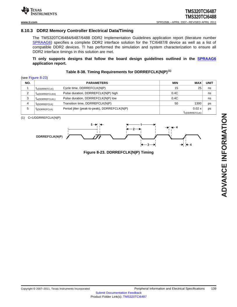
AD
VA
NC
E I
NF
OR
MA
TIO
N
2
1
3
4
4
DDRREFCLK(N|P)
5
TMS320TCI6487TMS320TCI6488
www.ti.com SPRS358L–APRIL 2007–REVISED APRIL 2011
8.10.3 DDR2 Memory Controller Electrical Data/Timing
The TMS320TCI6484/6487/6488 DDR2 Implementation Guidelines application report (literature numberSPRAAG6) specifies a complete DDR2 interface solution for the TCI6487/8 device as well as a list ofcompatible DDR2 devices. TI has performed the simulation and system characterization to ensure allDDR2 interface timings in this solution are met.
TI only supports designs that follow the board design guidelines outlined in the SPRAAG6application report.
Table 8-38. Timing Requirements for DDRREFCLK(N|P) (1)
(see Figure 8-23)
NO. PARAMETERS MIN MAX UNIT
1 tc(DDRREFCLK) Cycle time, DDRREFCLK(N|P) 15 25 ns
2 tw(DDRREFCLKH) Pulse duration, DDRREFCLK(N|P) high 0.4C ns
3 tw(DDRREFCLKL) Pulse duration, DDRREFCLK(N|P) low 0.4C ns
4 tt(DDRREFCLK) Transition time, DDRREFCLK(N|P) 50 1300 ps
5 tj(DDRREFCLK) Period jitter (peak-to-peak), DDRREFCLK(N|P) 0.02 x pstc(DDRREFCLK)
(1) C=1/DDRREFCLK(N|P)
Figure 8-23. DDRREFCLK(N|P) Timing
Copyright © 2007–2011, Texas Instruments Incorporated Peripheral Information and Electrical Specifications 139Submit Documentation Feedback
Product Folder Link(s): TMS320TCI6487

AD
VA
NC
E IN
FO
RM
AT
ION
TMS320TCI6487TMS320TCI6488SPRS358L–APRIL 2007–REVISED APRIL 2011 www.ti.com
8.11 I2C Peripheral
The inter-integrated circuit (I2C) module provides an interface between a C64x+ DSP and other devicescompliant with Philips Semiconductors Inter-IC bus (I2C bus) specification version 2.1 and connected byway of an I2C-bus. External components attached to this 2-wire serial bus can transmit/receive up to 8-bitdata to/from the DSP through the I2C module.
8.11.1 I2C Device-Specific Information
The TCI6487/8 device includes an I2C peripheral module (I2C). NOTE: when using the I2C module,ensure there are external pullup resistors on the SDA and SCL pins.
The I2C modules on the TCI6487/8 may be used by the DSP to control local peripherals ICs (DACs,ADCs, etc.) or may be used to communicate with other controllers in a system or to implement a userinterface.
The I2C port supports:• Compatible with Philips I2C Specification Revision 2.1 (January 2000)• Fast Mode up to 400 Kbps (no fail-safe I/O buffers)• Noise Filter to remove noise 50 ns or less• 7- and 10-Bit Device Addressing Modes• Multi-Master (Transmit/Receive) and Slave (Transmit/Receive) Functionality• Events: DMA, Interrupt, or Polling• Slew-Rate Limited Open-Drain Output Buffers
Figure 8-24 is a block diagram of the I2C module.
140 Peripheral Information and Electrical Specifications Copyright © 2007–2011, Texas Instruments Incorporated
Submit Documentation FeedbackProduct Folder Link(s): TMS320TCI6487

AD
VA
NC
E I
NF
OR
MA
TIO
N
TMS320TCI6487TMS320TCI6488
www.ti.com SPRS358L–APRIL 2007–REVISED APRIL 2011
Figure 8-24. I2C Module Block Diagram
Copyright © 2007–2011, Texas Instruments Incorporated Peripheral Information and Electrical Specifications 141Submit Documentation Feedback
Product Folder Link(s): TMS320TCI6487

AD
VA
NC
E IN
FO
RM
AT
ION
TMS320TCI6487TMS320TCI6488SPRS358L–APRIL 2007–REVISED APRIL 2011 www.ti.com
8.11.2 I2C Peripheral Register Description(s)
The memory map of the I2C is shown in Table 8-39.
Table 8-39. I2C Registers
HEX ADDRESS ACRONYM REGISTER NAME
02B0 4000 ICOAR I2C Own Address Register
02B0 4004 ICIMR I2C Interrupt Mask/Status Register
02B0 4008 ICSTR I2C Interrupt Status Register
02B0 400C ICCLKL I2C Clock Low-Time Divider Register
02B0 4010 ICCLKH I2C Clock High-Time Divider Register
02B0 4014 ICCNT I2C Data Count Register
02B0 4018 ICDRR I2C Data Receive Register
02B0 401C ICSAR I2C Slave Address Register
02B0 4020 ICDXR I2C Data Transmit Register
02B0 4024 ICMDR I2C Mode Register
02B0 4028 ICIVR I2C Interrupt Vector Register
02B0 402C ICEMDR I2C Extended Mode Register
02B0 4030 ICPSC I2C Prescaler Register
02B0 4034 ICPID1 I2C Peripheral Identification Register 1 [Value: 0x0000 0105]
02B0 4038 ICPID2 I2C Peripheral Identification Register 2 [Value: 0x0000 0005]
02B0 403C - 02B0 405C - Reserved
02B0 4060 - 02B0 407F - Reserved
02B0 4080 - 02B3 FFFF - Reserved
142 Peripheral Information and Electrical Specifications Copyright © 2007–2011, Texas Instruments Incorporated
Submit Documentation FeedbackProduct Folder Link(s): TMS320TCI6487

AD
VA
NC
E I
NF
OR
MA
TIO
N
TMS320TCI6487TMS320TCI6488
www.ti.com SPRS358L–APRIL 2007–REVISED APRIL 2011
8.11.3 I2C Electrical Data/Timing
Table 8-40. Timing Requirements for I2C Timings (1)
(see Figure 8-25)
NO. STANDARD MODE FAST MODE UNIT
MIN MAX MIN MAX
1 tc(SCL) Cycle time, SCL 10 2.5 μs
2 tsu(SCLH-SDAL) Setup time, SCL high before SDA low (for a 4.7 0.6 μsrepeated START condition)
3 th(SCLL-SDAL) Hold time, SCL low after SDA low (for a 4 0.6 μsSTART and a repeated START condition)
4 tw(SCLL) Pulse duration, SCL low 4.7 1.3 μs
5 tw(SCLH) Pulse duration, SCL high 4 0.6 μs
6 tsu(SDAV-SDLH) Setup time, SDA valid before SCL high 250 100 (2) μs
7 th(SDA-SDLL) Hold time, SDA valid after SCL low (for I2C 0 (3) 0 0.9 (4) μsbus™ devices)
8 tw(SDAH) Pulse duration, SDA high between STOP and 4.7 1.3 μsSTART conditions.
9 tr(SDA) Rise time, SDA 1000 20 + 0.1Cb 300 ns
10 tr(SCL) Rise time, SCL 1000 20 + 0.1Cb 300 ns
11 tf(SDA) Fall time, SDA 300 20 + 0.1Cb 300 ns
12 tf(SCL) Fall time, SCL 300 20 + 0.1Cb 300 ns
13 tsu(SCLH-SDAH) Setup time, SCL high before SDA high (for 4 0.6 μsSTOP condition)
14 tw(SP) Pulse duration, spike (must be suppressed) 0 50 ns
15 Cb(5) Capacitive load for each bus line 400 400 pF
(1) The I2C pins SDA and SCL do not feature fail-safe I/O buffers. These pins could potentially draw current when the device is powereddown.
(2) A fast-mode I2C-bus device can be used in a standard-mode I2C-bus system, but the requirement, tsu(SDA-SCLH)≥ 250 ns, must then bemet. This will automatically be the case if the device does not stretch the LOW period of the SCL signal. If such a device does stretchthe LOW period of the SCL signal, it must output the next data bit to the SDA line, Tr max + Tsu(SDA-SCLH) = 1000 + 250 + 1250 ns(according to the standard-mode I2C-bus specification), before the SCL line is released.
(3) A device must internally provide a hold time of at least 300 ns for the SDA signal (referred to the VIHmin of the SCL signal) to bridge theundefined region of the falling edge of SCL.
(4) The maximum, th(SDA-SCLL), has only to be met if the device does not stretch the low period, tw(SCLL), of the SCL signal.(5) Cb = total capacitance of one bus line, in pF. If mixed with HS-mode devices, faster fall-times are allowed.
Figure 8-25. I2C Receive Timings
Copyright © 2007–2011, Texas Instruments Incorporated Peripheral Information and Electrical Specifications 143Submit Documentation Feedback
Product Folder Link(s): TMS320TCI6487
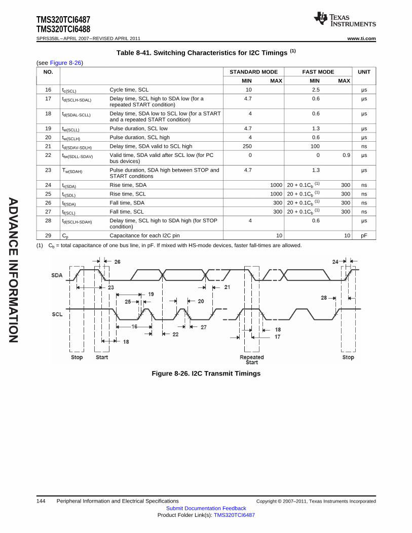
AD
VA
NC
E IN
FO
RM
AT
ION
TMS320TCI6487TMS320TCI6488SPRS358L–APRIL 2007–REVISED APRIL 2011 www.ti.com
Table 8-41. Switching Characteristics for I2C Timings (1)
(see Figure 8-26)
NO. STANDARD MODE FAST MODE UNIT
MIN MAX MIN MAX
16 tc(SCL) Cycle time, SCL 10 2.5 μs
17 td(SCLH-SDAL) Delay time, SCL high to SDA low (for a 4.7 0.6 μsrepeated START condition)
18 td(SDAL-SCLL) Delay time, SDA low to SCL low (for a START 4 0.6 μsand a repeated START condition)
19 tw(SCLL) Pulse duration, SCL low 4.7 1.3 μs
20 tw(SCLH) Pulse duration, SCL high 4 0.6 μs
21 td(SDAV-SDLH) Delay time, SDA valid to SCL high 250 100 ns
22 ttw(SDLL-SDAV) Valid time, SDA valid after SCL low (for PC 0 0 0.9 μsbus devices)
23 Tw(SDAH) Pulse duration, SDA high between STOP and 4.7 1.3 μsSTART conditions
24 tr(SDA) Rise time, SDA 1000 20 + 0.1Cb(1) 300 ns
25 tr(SDL) Rise time, SCL 1000 20 + 0.1Cb(1) 300 ns
26 tf(SDA) Fall time, SDA 300 20 + 0.1Cb(1) 300 ns
27 tf(SCL) Fall time, SCL 300 20 + 0.1Cb(1) 300 ns
28 td(SCLH-SDAH) Delay time, SCL high to SDA high (for STOP 4 0.6 μscondition)
29 Cp Capacitance for each I2C pin 10 10 pF
(1) Cb = total capacitance of one bus line, in pF. If mixed with HS-mode devices, faster fall-times are allowed.
Figure 8-26. I2C Transmit Timings
144 Peripheral Information and Electrical Specifications Copyright © 2007–2011, Texas Instruments Incorporated
Submit Documentation FeedbackProduct Folder Link(s): TMS320TCI6487

AD
VA
NC
E I
NF
OR
MA
TIO
N
1
0
1
0
CLKS
chip_clksCPU/ ,
Where = 8 to 32n
n
Internal Clock SourceCPU/6
DEVCFG.CLKS0/1
CLKSRG
CLKSM
TMS320TCI6487TMS320TCI6488
www.ti.com SPRS358L–APRIL 2007–REVISED APRIL 2011
8.12 Multichannel Buffered Serial Port (McBSP)
The McBSP provides these functions:• Full-duplex communication• Double-buffered data registers, which allow a continuous data stream• Independent framing and clocking for receive and transmit• Direct interface to industry-standard codecs, analog interface chips (AICs), and other serially
connected analog-to-digital (A/D) and digital-to-analog (D/A) devices• External shift clock or an internal, programmable frequency shift clock for data transfer• SPI operation in master mode only
For more detailed information on the McBSP peripheral, see the TMS320C6472/TMS320TCI648x DSPMultichannel Buffered Serial Port (McBSP) Reference Guide (literature number SPRU803).
8.12.1 McBSP Device-Specific Information
The CLKS signal for MCBSP0 and MCBSP1 can be sourced from an external pin or by PLL Controller 1.For details, see Section 8.8. If the clock from the PLL Controller 1 is used, the clock is shared between thetwo McBSPs.Figure 8-27 shows the sample rate generator clock (CLKSRG) selection logical diagram.
A. For more details, see SYSCLK11 description in Section 8.8.1.1.
Figure 8-27. Sample Rate Generator Clock (CLKSRG)
8.12.2 McBSP Peripheral Register Descriptions
The memory map of the McBSP 0 registers is shown in Table 8-42.
Table 8-42. McBSP 0 Registers
HEX ADDRESS ACRONYM REGISTER NAME
028C 0000 DRR0 McBSP0 Data Receive Register via Configuration Bus.Note: The CPU and EDMA3 controller can only read this register; they can notwrite to it.
3000 0000 DRR0 McBSP0 Data Receive Register via EDMA3 Bus
028C 0004 DXR0 McBSP0 Data Transmit Register via Configuration Bus
3000 0010 DXR0 McBSP0 Data Transmit register via EDMA bus
028C 0008 SPCR0 McBSP0 Serial Port Control Register
028C 000C RCR0 McBSP0 Receive Control Register
028C 0010 XCR0 McBSP0 Transmit Control Register
028C 0014 SRGR0 McBSP0 Sample Rate Generator Register
028C 0018 MCR0 McBSP0 Multichannel Control Register
028C 001C RCERE00 McBSP0 Enhanced Receive Channel Enable Register 0 Partition A/B
028C 0020 XCERE00 McBSP0 Enhanced Transmit Channel Enable Register 0 Partition A/B
028C 0024 PCR0 McBSP0 Pin Control Register
Copyright © 2007–2011, Texas Instruments Incorporated Peripheral Information and Electrical Specifications 145Submit Documentation Feedback
Product Folder Link(s): TMS320TCI6487

AD
VA
NC
E IN
FO
RM
AT
ION
TMS320TCI6487TMS320TCI6488SPRS358L–APRIL 2007–REVISED APRIL 2011 www.ti.com
Table 8-42. McBSP 0 Registers (continued)
HEX ADDRESS ACRONYM REGISTER NAME
028C 0028 RCERE10 McBSP0 Enhanced Receive Channel Enable Register 0 Partition C/D
028C 002C XCERE10 McBSP0 Enhanced Transmit Channel Enable Register 0 Partition C/D
028C 0030 RCERE20 McBSP0 Enhanced Receive Channel Enable Register 0 Partition E/F
028C 0034 XCERE20 McBSP0 Enhanced Transmit Channel Enable Register 0 Partition E/F
028C 0038 RCERE30 McBSP0 Enhanced Receive Channel Enable Register 0 Partition G/H
028C 003C XCERE30 McBSP0 Enhanced Transmit Channel Enable Register 0 Partition G/H
028C 0040 - 028C 00FF - Reserved
The memory map of the McBSP 1 registers is shown in Table 8-43.
Table 8-43. McBSP 1 Registers
HEX ADDRESS ACRONYM REGISTER NAME
028D 0000 DRR1 McBSP1 Data Receive Register via Configuration Bus.Note: The CPU and EDMA3 controller can only read this register; they can notwrite to it.
3400 0000 DRR1 McBSP1 Data Receive Register via EDMA3 Bus
028D 0004 DXR1 McBSP1 Data Transmit Register via Configuration Bus
3400 0010 DXR1 McBSP1 Data Transmit Register via EDMA Bus
028D 0008 SPCR1 McBSP1 Serial Port Control Register
028D 000C RCR1 McBSP1 Receive Control Register
028D 0010 XCR1 McBSP1 Transmit Control Register
028D 0014 SRGR1 McBSP1 Sample Rate Generator Register
028D 0018 MCR1 McBSP1 Multichannel Control Register
028D 001C RCERE01 McBSP1 Enhanced Receive Channel Enable Register 0 Partition A/B
028D 0020 XCERE01 McBSP1 Enhanced Transmit Channel Enable Register 0 Partition A/B
028D 0024 PCR1 McBSP1 Pin Control Register
028D 0028 RCERE11 McBSP1 Enhanced Receive Channel Enable Register 0 Partition C/D
028D 002C XCERE11 McBSP1 Enhanced Transmit Channel Enable Register 0 Partition C/D
028D 0030 RCERE21 McBSP1 Enhanced Receive Channel Enable Register 0 Partition E/F
028D 0034 XCERE21 McBSP1 Enhanced Transmit Channel Enable Register 0 Partition E/F
028D 0038 RCERE31 McBSP1 Enhanced Receive Channel Enable Register 0 Partition G/H
028D 003C XCERE3 McBSP1 Enhanced Transmit Channel Enable Register 0 Partition G/H
028D 0040 - 028D 00FF - Reserved
146 Peripheral Information and Electrical Specifications Copyright © 2007–2011, Texas Instruments Incorporated
Submit Documentation FeedbackProduct Folder Link(s): TMS320TCI6487
AD
VA
NC
E I
NF
OR
MA
TIO
N
TMS320TCI6487TMS320TCI6488
www.ti.com SPRS358L–APRIL 2007–REVISED APRIL 2011
8.12.3 McBSP Electrical Data/Timing
Table 8-44. Timing Requirements for McBSP (1)
(see Figure 8-28)
NO. MIN MAX UNIT
2 tc(CKRX) Cycle time, CLKR/X CLKR/X ext 10P (2) ns
3 tw(CKRX) Pulse duration, CLKR/X high or CLKR/X low CLKR/X ext 0.5t c(CKRX)-1(2) ns
5 tsu(FRH-CKRL) Setup time, external FSR high before CLKR low CLKR int 9 ns
CLKR ext 1.3
6 th(CKRL-FRH) Hold time, external FSR high after CLKR low CLKR int 6 ns
CLKR ext 3
7 tsu(DRV-CKRL) Setup time, DR valid before CLKR low CLKR int 8 ns
CLKR ext 0.9
8 th(CKRL-DRV) Hold time, DR valid after CLKR low CLKR int 3 ns
CLKR ext 3.1
10 tsu(FXH-CKXL) Setup time, external FSX high before CLKX low CLKR int 9 ns
CLKR ext 1.3
11 th(CKXL-FXH) Hold time, external FSX high after CLKX low CLKR int 6 ns
CLKR ext 3
(1) P = 1/CPU Clock in ns.(2) This parameter applies to the maximum McBSP frequency. Operate serial clocks (CLKR/X) in the reasonable range of 40/60 duty
cycles.
Copyright © 2007–2011, Texas Instruments Incorporated Peripheral Information and Electrical Specifications 147Submit Documentation Feedback
Product Folder Link(s): TMS320TCI6487

AD
VA
NC
E IN
FO
RM
AT
ION
TMS320TCI6487TMS320TCI6488SPRS358L–APRIL 2007–REVISED APRIL 2011 www.ti.com
Table 8-45. Switching Characteristics Over Recommended Operating Conditions for McBSP (1) (2)
(see Figure 8-28)
NO. MIN MAX UNIT
1 td(CKSH-CKRXH) Delay time, CLKS high to CLKR/X high for internal CLKR/X 1.4 10 nsgenerated from CLKS input. (3)
2 tc(CKRX) Cycle time, CLKR/X CLKR/X int 10P (4) ns
3 tw(CKRX) Pulse duration, CLKR/X high or CLKR/X int C - 1 (5) C + 1 (5) nsCLKR/X low
4 td(CKRH-FRV) Delay time, CLKR high to internal CLKR int -2.1 3 nsFSR valid
9 td(CKXH-FXV) Delay time, CLKX high to internal CLKX int -1.7 3 nsFSX valid CLKX ext 1.7 9
12 tdis(CKXH-DXHZ) Disable time, DX high impedance CLKX int -3.9 4 nsfollowing last data bit from CLKX CLKX ext 2.1 9high
CLKX int -3.9 +D1 (6) 4 + D2 (6) ns
13 td(CKXH-DXV) Delay time, CLKX high to DX valid CLKX ext (DXENA = 0) 2.1 (6) 9 (6)
CLKX ext (DXENA = 1) 2.1 + D1 (6) 9 + D2 (6)
Delay time, FSX high to DX valid FSX int -2.3 + D1 (7) 5.6 + D2 (7) ns14 td(FXH-DXV) ONLY applies when in data delay FSX ext 1.9 + D1 (7) 9 + D2 (7)
0 (XDATDLY = 00b)mode
(1) CLKRP = CLKXP = FSRP = FSXP = 0. If polarity of any of the signals is inverted, then the timing references of that signal are alsoinverted.
(2) Minimum delay times also represent minimum output hold times.(3) The CLKS signal is shared by both McBSP0 and McBSP1 on this device.(4) P = 1/CPU clock frequency, in ns. For example, when running parts at 1000 MHz, use P = 1 ns.(5) C = H or L S = sample rate generator input clock = 6P if CLKSM = 1 (P = 1/CPU clock frequency)
S = sample rate generator input clock = P_clks if CLKSM = 0 (P_clks = CLKS period)H = CLKX high pulse width = (CLKGDV/2 + 1) * S if CLKGDV is evenH = (CLKGDV + 1)/2 * S if CLKGDV is odd L = CLKX low pulse width = (CLKGDV/2) * S if CLKGDV is evenL = (CLKGDV + 1)/2 * S if CLKGDV is odd CLKGDV should be set appropriately to ensure the McBSP bit rate does not exceed themaximum limit (see (4) above).
(6) Extra delay from CLKX high to DX valid applies only to the first data bit of a device, if and only if DXENA = 1 in SPCR.if DXENA = 0, then D1 = D2 = 0if DXENA = 1, then D1 = 6P, D2 = 12P
(7) Extra delay from FSX high to DX valid applies only to the first data bit of a device, if and only if DXENA = 1 in SPCR.if DXENA = 0, then D1 = D2 = 0if DXENA = 1, then D1 = 6P, D2 = 12P
148 Peripheral Information and Electrical Specifications Copyright © 2007–2011, Texas Instruments Incorporated
Submit Documentation FeedbackProduct Folder Link(s): TMS320TCI6487
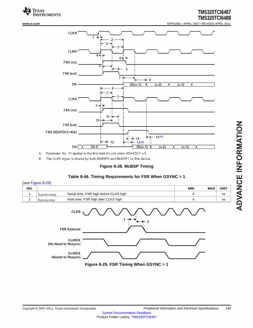
AD
VA
NC
E I
NF
OR
MA
TIO
N
12
CLKS
FSR External
CLKR/X(No Need to Resync)
CLKR/X(Needs to Resync)
TMS320TCI6487TMS320TCI6488
www.ti.com SPRS358L–APRIL 2007–REVISED APRIL 2011
Figure 8-28. McBSP Timing
Table 8-46. Timing Requirements for FSR When GSYNC = 1(see Figure 8-29)
NO. MIN MAX UNIT
1 tsu(FRH-CKSH) Setup time, FSR high before CLKS high 4 ns
2 th(CKSH-FRH) Hold time, FSR high after CLKS high 4 ns
Figure 8-29. FSR Timing When GSYNC = 1
Copyright © 2007–2011, Texas Instruments Incorporated Peripheral Information and Electrical Specifications 149Submit Documentation Feedback
Product Folder Link(s): TMS320TCI6487
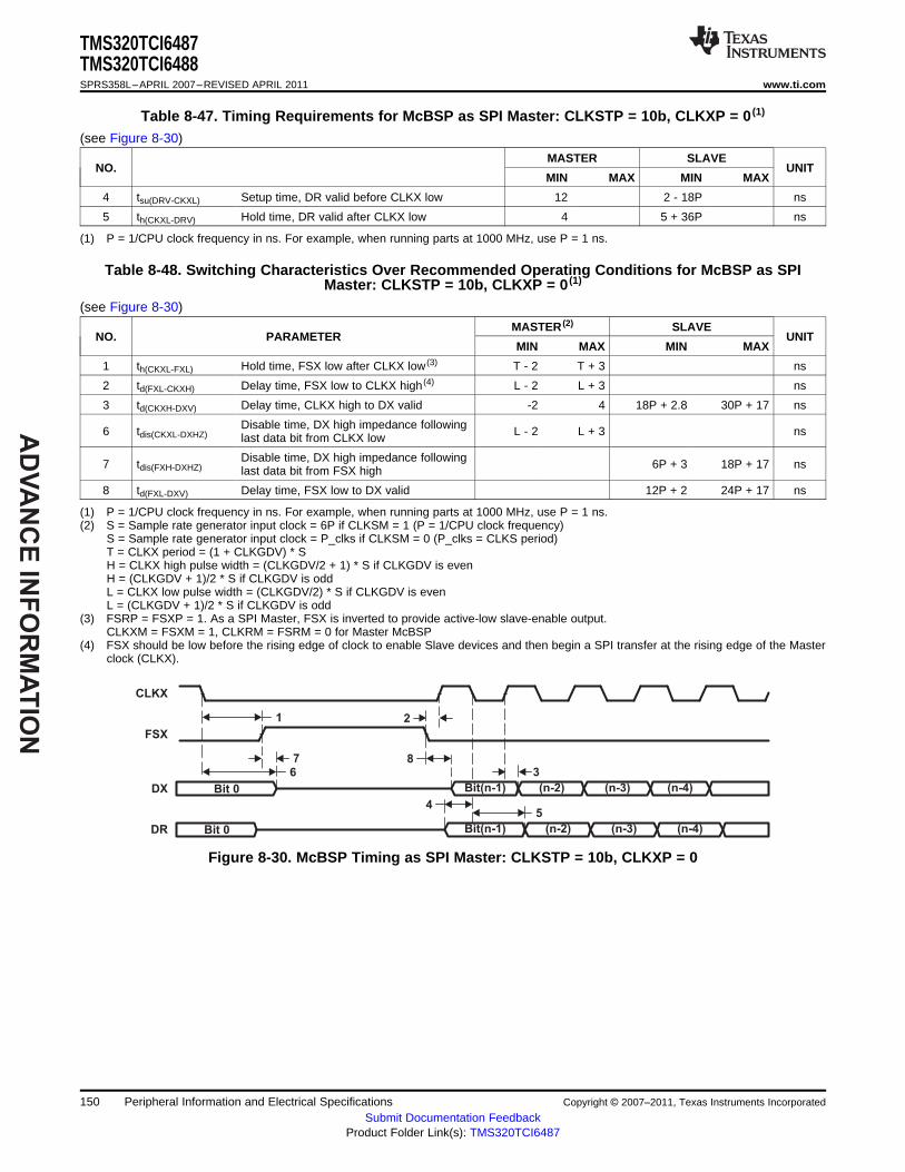
AD
VA
NC
E IN
FO
RM
AT
ION
Bit 0 Bit(n-1) (n-2) (n-3) (n-4)
Bit 0 Bit(n-1) (n-2) (n-3) (n-4)
54
387
6
21
CLKX
FSX
DX
DR
TMS320TCI6487TMS320TCI6488SPRS358L–APRIL 2007–REVISED APRIL 2011 www.ti.com
Table 8-47. Timing Requirements for McBSP as SPI Master: CLKSTP = 10b, CLKXP = 0 (1)
(see Figure 8-30)
MASTER SLAVENO. UNIT
MIN MAX MIN MAX
4 tsu(DRV-CKXL) Setup time, DR valid before CLKX low 12 2 - 18P ns
5 th(CKXL-DRV) Hold time, DR valid after CLKX low 4 5 + 36P ns
(1) P = 1/CPU clock frequency in ns. For example, when running parts at 1000 MHz, use P = 1 ns.
Table 8-48. Switching Characteristics Over Recommended Operating Conditions for McBSP as SPIMaster: CLKSTP = 10b, CLKXP = 0 (1)
(see Figure 8-30)
MASTER (2) SLAVENO. PARAMETER UNIT
MIN MAX MIN MAX
1 th(CKXL-FXL) Hold time, FSX low after CLKX low (3) T - 2 T + 3 ns
2 td(FXL-CKXH) Delay time, FSX low to CLKX high (4) L - 2 L + 3 ns
3 td(CKXH-DXV) Delay time, CLKX high to DX valid -2 4 18P + 2.8 30P + 17 ns
Disable time, DX high impedance following6 tdis(CKXL-DXHZ) L - 2 L + 3 nslast data bit from CLKX low
Disable time, DX high impedance following7 tdis(FXH-DXHZ) 6P + 3 18P + 17 nslast data bit from FSX high
8 td(FXL-DXV) Delay time, FSX low to DX valid 12P + 2 24P + 17 ns
(1) P = 1/CPU clock frequency in ns. For example, when running parts at 1000 MHz, use P = 1 ns.(2) S = Sample rate generator input clock = 6P if CLKSM = 1 (P = 1/CPU clock frequency)
S = Sample rate generator input clock = P_clks if CLKSM = 0 (P_clks = CLKS period)T = CLKX period = (1 + CLKGDV) * SH = CLKX high pulse width = (CLKGDV/2 + 1) * S if CLKGDV is evenH = (CLKGDV + 1)/2 * S if CLKGDV is oddL = CLKX low pulse width = (CLKGDV/2) * S if CLKGDV is evenL = (CLKGDV + 1)/2 * S if CLKGDV is odd
(3) FSRP = FSXP = 1. As a SPI Master, FSX is inverted to provide active-low slave-enable output.CLKXM = FSXM = 1, CLKRM = FSRM = 0 for Master McBSP
(4) FSX should be low before the rising edge of clock to enable Slave devices and then begin a SPI transfer at the rising edge of the Masterclock (CLKX).
Figure 8-30. McBSP Timing as SPI Master: CLKSTP = 10b, CLKXP = 0
150 Peripheral Information and Electrical Specifications Copyright © 2007–2011, Texas Instruments Incorporated
Submit Documentation FeedbackProduct Folder Link(s): TMS320TCI6487
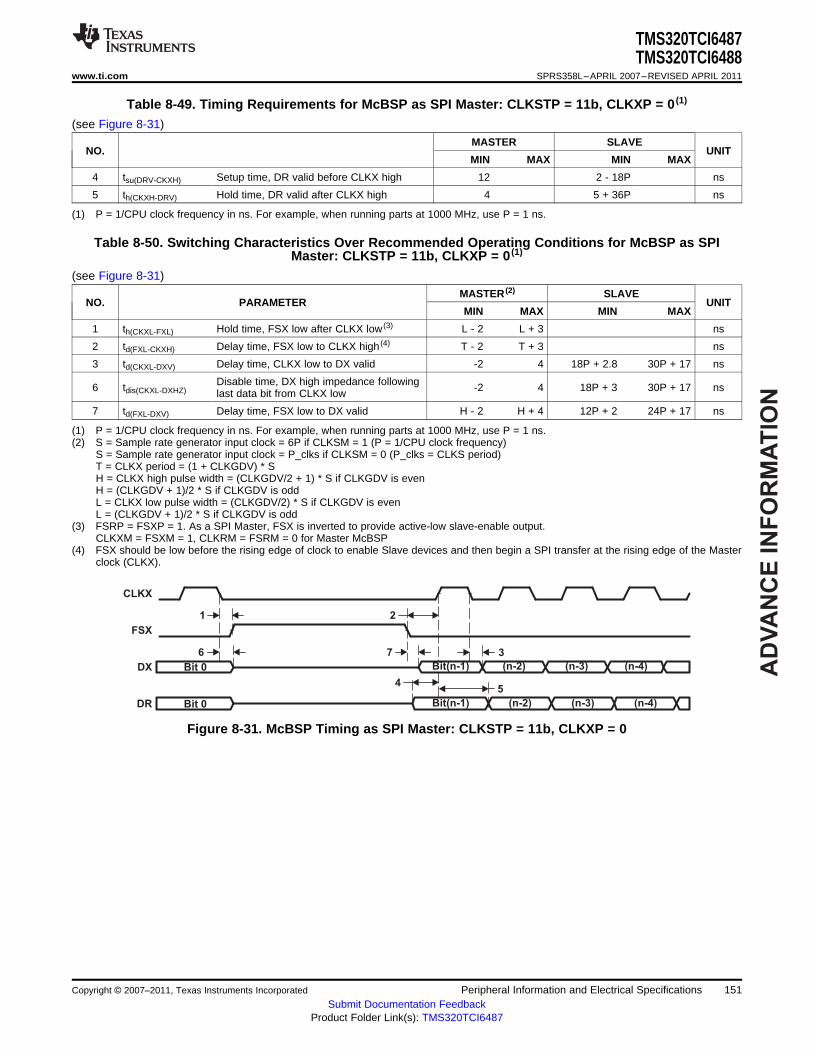
AD
VA
NC
E I
NF
OR
MA
TIO
N
Bit 0 Bit(n-1) (n-2) (n-3) (n-4)
Bit 0 Bit(n-1) (n-2) (n-3) (n-4)
4
376
21
CLKX
FSX
DX
DR
5
TMS320TCI6487TMS320TCI6488
www.ti.com SPRS358L–APRIL 2007–REVISED APRIL 2011
Table 8-49. Timing Requirements for McBSP as SPI Master: CLKSTP = 11b, CLKXP = 0 (1)
(see Figure 8-31)
MASTER SLAVENO. UNIT
MIN MAX MIN MAX
4 tsu(DRV-CKXH) Setup time, DR valid before CLKX high 12 2 - 18P ns
5 th(CKXH-DRV) Hold time, DR valid after CLKX high 4 5 + 36P ns
(1) P = 1/CPU clock frequency in ns. For example, when running parts at 1000 MHz, use P = 1 ns.
Table 8-50. Switching Characteristics Over Recommended Operating Conditions for McBSP as SPIMaster: CLKSTP = 11b, CLKXP = 0 (1)
(see Figure 8-31)
MASTER (2) SLAVENO. PARAMETER UNIT
MIN MAX MIN MAX
1 th(CKXL-FXL) Hold time, FSX low after CLKX low (3) L - 2 L + 3 ns
2 td(FXL-CKXH) Delay time, FSX low to CLKX high (4) T - 2 T + 3 ns
3 td(CKXL-DXV) Delay time, CLKX low to DX valid -2 4 18P + 2.8 30P + 17 ns
Disable time, DX high impedance following6 tdis(CKXL-DXHZ) -2 4 18P + 3 30P + 17 nslast data bit from CLKX low
7 td(FXL-DXV) Delay time, FSX low to DX valid H - 2 H + 4 12P + 2 24P + 17 ns
(1) P = 1/CPU clock frequency in ns. For example, when running parts at 1000 MHz, use P = 1 ns.(2) S = Sample rate generator input clock = 6P if CLKSM = 1 (P = 1/CPU clock frequency)
S = Sample rate generator input clock = P_clks if CLKSM = 0 (P_clks = CLKS period)T = CLKX period = (1 + CLKGDV) * SH = CLKX high pulse width = (CLKGDV/2 + 1) * S if CLKGDV is evenH = (CLKGDV + 1)/2 * S if CLKGDV is oddL = CLKX low pulse width = (CLKGDV/2) * S if CLKGDV is evenL = (CLKGDV + 1)/2 * S if CLKGDV is odd
(3) FSRP = FSXP = 1. As a SPI Master, FSX is inverted to provide active-low slave-enable output.CLKXM = FSXM = 1, CLKRM = FSRM = 0 for Master McBSP
(4) FSX should be low before the rising edge of clock to enable Slave devices and then begin a SPI transfer at the rising edge of the Masterclock (CLKX).
Figure 8-31. McBSP Timing as SPI Master: CLKSTP = 11b, CLKXP = 0
Copyright © 2007–2011, Texas Instruments Incorporated Peripheral Information and Electrical Specifications 151Submit Documentation Feedback
Product Folder Link(s): TMS320TCI6487

AD
VA
NC
E IN
FO
RM
AT
ION
Bit 0 Bit(n-1) (n-2) (n-3) (n-4)
Bit 0 Bit(n-1) (n-2) (n-3) (n-4)
54
387
6
21
CLKX
FSX
DX
DR
TMS320TCI6487TMS320TCI6488SPRS358L–APRIL 2007–REVISED APRIL 2011 www.ti.com
Table 8-51. Timing Requirements for McBSP as SPI Master: CLKSTP = 10b, CLKXP = 1 (1)
(see Figure 8-32)
MASTER SLAVENO. UNIT
MIN MAX MIN MAX
4 tsu(DRV-CKXH) Setup time, DR valid before CLKX high 12 2 - 18P ns
5 th(CKXH-DRV) Hold time, DR valid after CLKX high 4 5 + 36P ns
(1) P = 1/CPU clock frequency in ns. For example, when running parts at 1000 MHz, use P = 1 ns.
Table 8-52. Switching Characteristics Over Recommended Operating Conditions for McBSP as SPIMaster: CLKSTP = 10b, CLKXP = 1 (1)
(see Figure 8-32)
MASTER (2) SLAVENO. PARAMETER UNIT
MIN MAX MIN MAX
1 th(CKXH-FXL) Hold time, FSX low after CLKX high (3) T - 2 T + 3 ns
2 td(FXL-CKXL) Delay time, FSX low to CLKX low (4) H - 2 H + 3 ns
3 td(CKXL-DXV) Delay time, CLKX low to DX valid -2 4 18P + 2.8 30P + 17 ns
Disable time, DX high impedance following6 tdis(CKXH-DXHZ) H - 2 H + 3 nslast data bit from CLKX high
Disable time, DX high impedance following7 tdis(FXH-DXHZ) 6P + 3 18P + 17 nslast data bit from FSX high
8 td(FXL-DXV) Delay time, FSX low to DX valid 12P + 2 24P + 17 ns
(1) P = 1/CPU clock frequency in ns. For example, when running parts at 1000 MHz, use P = 1 ns.(2) S = Sample rate generator input clock = 6P if CLKSM = 1 (P = 1/CPU clock frequency)
S = Sample rate generator input clock = P_clks if CLKSM = 0 (P_clks = CLKS period)T = CLKX period = (1 + CLKGDV) * SH = CLKX high pulse width = (CLKGDV/2 + 1) * S if CLKGDV is evenH = (CLKGDV + 1)/2 * S if CLKGDV is oddL = CLKX low pulse width = (CLKGDV/2) * S if CLKGDV is evenL = (CLKGDV + 1)/2 * S if CLKGDV is odd
(3) FSRP = FSXP = 1. As a SPI Master, FSX is inverted to provide active-low slave-enable output.CLKXM = FSXM = 1, CLKRM = FSRM = 0 for Master McBSP
(4) FSX should be low before the rising edge of clock to enable Slave devices and then begin a SPI transfer at the rising edge of the Masterclock (CLKX).
Figure 8-32. McBSP Timing as SPI Master: CLKSTP = 10b, CLKXP = 1
152 Peripheral Information and Electrical Specifications Copyright © 2007–2011, Texas Instruments Incorporated
Submit Documentation FeedbackProduct Folder Link(s): TMS320TCI6487

AD
VA
NC
E I
NF
OR
MA
TIO
N
Bit 0 Bit(n-1) (n-2) (n-3) (n-4)
Bit 0 Bit(n-1) (n-2) (n-3) (n-4)
54
376
21
CLKX
FSX
DX
DR
TMS320TCI6487TMS320TCI6488
www.ti.com SPRS358L–APRIL 2007–REVISED APRIL 2011
Table 8-53. Timing Requirements for McBSP as SPI Master: CLKSTP = 11b, CLKXP = 1 (1)
(see Figure 8-33)
MASTER SLAVENO. UNIT
MIN MAX MIN MAX
4 tsu(DRV-CKXH) Setup time, DR valid before CLKX high 12 2 - 18P ns
5 th(CKXH-DRV) Hold time, DR valid after CLKX high 4 5 + 36P ns
(1) P = 1/CPU clock frequency in ns. For example, when running parts at 1000 MHz, use P = 1 ns.
Table 8-54. Switching Characteristics Over Recommended Operating Conditions for McBSP as SPIMaster: CLKSTP = 11b, CLKXP = 1 (1)
(see Figure 8-33)
MASTER (2) SLAVENO. PARAMETER UNIT
MIN MAX MIN MAX
1 th(CKXH-FXL) Hold time, FSX low after CLKX high (3) H - 2 H + 3 ns
2 td(FXL-CKXL) Delay time, FSX low to CLKX low (4) T - 2 T + 1 ns
3 td(CKXH-DXV) Delay time, CLKX high to DX valid -2 4 18P + 2.8 30P + 17 ns
Disable time, DX high impedance following6 tdis(CKXH-DXHZ) -2 4 18P + 3 30P + 17 nslast data bit from CLKX high
7 td(FXL-DXV) Delay time, FSX low to DX valid L - 2 L + 4 12P + 2 24P + 17 ns
(1) P = 1/CPU clock frequency in ns. For example, when running parts at 1000 MHz, use P = 1 ns.(2) S = Sample rate generator input clock = 6P if CLKSM = 1 (P = 1/CPU clock frequency)
S = Sample rate generator input clock = P_clks if CLKSM = 0 (P_clks = CLKS period)T = CLKX period = (1 + CLKGDV) * SH = CLKX high pulse width = (CLKGDV/2 + 1) * S if CLKGDV is evenH = (CLKGDV + 1)/2 * S if CLKGDV is oddL = CLKX low pulse width = (CLKGDV/2) * S if CLKGDV is evenL = (CLKGDV + 1)/2 * S if CLKGDV is odd
(3) FSRP = FSXP = 1. As a SPI Master, FSX is inverted to provide active-low slave-enable output.CLKXM = FSXM = 1, CLKRM = FSRM = 0 for Master McBSP
(4) FSX should be low before the rising edge of clock to enable Slave devices and then begin a SPI transfer at the rising edge of the Masterclock (CLKX).
Figure 8-33. McBSP Timing as SPI Master: CLKSTP = 11b, CLKXP = 1
Copyright © 2007–2011, Texas Instruments Incorporated Peripheral Information and Electrical Specifications 153Submit Documentation Feedback
Product Folder Link(s): TMS320TCI6487

AD
VA
NC
E IN
FO
RM
AT
ION
TMS320TCI6487TMS320TCI6488SPRS358L–APRIL 2007–REVISED APRIL 2011 www.ti.com
8.13 Ethernet MAC (EMAC)
The Ethernet Media Access Controller (EMAC) module provides an efficient interface between theTCI6487/8 DSP core processor and the networked community. The EMAC supports 1000BaseT (1000Mbps) in full-duplex mode, with hardware flow control and quality-of-service (QOS) support.
The EMAC module conforms to the IEEE 802.3-2002 standard, describing the “Carrier Sense MultipleAccess with Collision Detection (CSMA/CD) Access Method and Physical Layer” specifications. The IEEE802.3 standard has also been adopted by ISO/IEC and re-designated as ISO/IEC 8802-3:2000(E).
Deviation from this standard, the EMAC module does not use the Transmit Coding Error signal MTXER.Instead of driving the error pin when an underflow condition occurs on a transmitted frame, the EMAC willintentionally generate an incorrect checksum by inverting the frame CRC, so that the transmitted framewill be detected as an error by the network.
The EMAC control module is the main interface between the device core processor, the MDIO module,and the EMAC module. The relationship between these three components is shown in Figure 8-34. TheEMAC control module contains the necessary components to allow the EMAC to make efficient use ofdevice memory, plus it controls device interrupts. The EMAC control module incorporates 8K-bytes ofinternal RAM to hold EMAC buffer descriptors.
Figure 8-34. EMAC, MDIO, and EMAC Control Modules
For more detailed information on the EMAC/MDIO, see the TMS320TCI6487/8 DSP EMAC/MDIO ModuleReference Guide (literature number SPRUEF0).
8.13.1 EMAC Device-Specific Information
The EMAC module on the device supports Serial Gigabit Media Independent Interface (SGMII). TheSGMII interface conforms to version 1.8 of the industry standard specification.
154 Peripheral Information and Electrical Specifications Copyright © 2007–2011, Texas Instruments Incorporated
Submit Documentation FeedbackProduct Folder Link(s): TMS320TCI6487
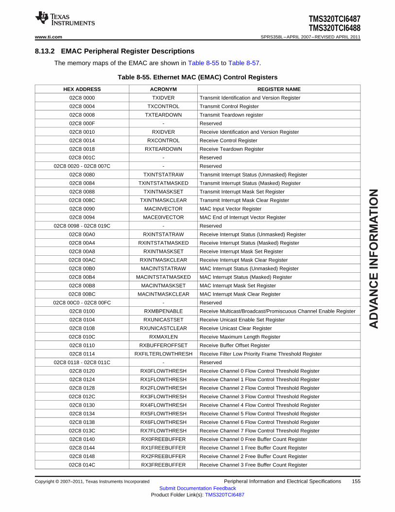
AD
VA
NC
E I
NF
OR
MA
TIO
N
TMS320TCI6487TMS320TCI6488
www.ti.com SPRS358L–APRIL 2007–REVISED APRIL 2011
8.13.2 EMAC Peripheral Register Descriptions
The memory maps of the EMAC are shown in Table 8-55 to Table 8-57.
Table 8-55. Ethernet MAC (EMAC) Control Registers
HEX ADDRESS ACRONYM REGISTER NAME
02C8 0000 TXIDVER Transmit Identification and Version Register
02C8 0004 TXCONTROL Transmit Control Register
02C8 0008 TXTEARDOWN Transmit Teardown register
02C8 000F - Reserved
02C8 0010 RXIDVER Receive Identification and Version Register
02C8 0014 RXCONTROL Receive Control Register
02C8 0018 RXTEARDOWN Receive Teardown Register
02C8 001C - Reserved
02C8 0020 - 02C8 007C - Reserved
02C8 0080 TXINTSTATRAW Transmit Interrupt Status (Unmasked) Register
02C8 0084 TXINTSTATMASKED Transmit Interrupt Status (Masked) Register
02C8 0088 TXINTMASKSET Transmit Interrupt Mask Set Register
02C8 008C TXINTMASKCLEAR Transmit Interrupt Mask Clear Register
02C8 0090 MACINVECTOR MAC Input Vector Register
02C8 0094 MACE0IVECTOR MAC End of Interrupt Vector Register
02C8 0098 - 02C8 019C - Reserved
02C8 00A0 RXINTSTATRAW Receive Interrupt Status (Unmasked) Register
02C8 00A4 RXINTSTATMASKED Receive Interrupt Status (Masked) Register
02C8 00A8 RXINTMASKSET Receive Interrupt Mask Set Register
02C8 00AC RXINTMASKCLEAR Receive Interrupt Mask Clear Register
02C8 00B0 MACINTSTATRAW MAC Interrupt Status (Unmasked) Register
02C8 00B4 MACINTSTATMASKED MAC Interrupt Status (Masked) Register
02C8 00B8 MACINTMASKSET MAC Interrupt Mask Set Register
02C8 00BC MACINTMASKCLEAR MAC Interrupt Mask Clear Register
02C8 00C0 - 02C8 00FC - Reserved
02C8 0100 RXMBPENABLE Receive Multicast/Broadcast/Promiscuous Channel Enable Register
02C8 0104 RXUNICASTSET Receive Unicast Enable Set Register
02C8 0108 RXUNICASTCLEAR Receive Unicast Clear Register
02C8 010C RXMAXLEN Receive Maximum Length Register
02C8 0110 RXBUFFEROFFSET Receive Buffer Offset Register
02C8 0114 RXFILTERLOWTHRESH Receive Filter Low Priority Frame Threshold Register
02C8 0118 - 02C8 011C - Reserved
02C8 0120 RX0FLOWTHRESH Receive Channel 0 Flow Control Threshold Register
02C8 0124 RX1FLOWTHRESH Receive Channel 1 Flow Control Threshold Register
02C8 0128 RX2FLOWTHRESH Receive Channel 2 Flow Control Threshold Register
02C8 012C RX3FLOWTHRESH Receive Channel 3 Flow Control Threshold Register
02C8 0130 RX4FLOWTHRESH Receive Channel 4 Flow Control Threshold Register
02C8 0134 RX5FLOWTHRESH Receive Channel 5 Flow Control Threshold Register
02C8 0138 RX6FLOWTHRESH Receive Channel 6 Flow Control Threshold Register
02C8 013C RX7FLOWTHRESH Receive Channel 7 Flow Control Threshold Register
02C8 0140 RX0FREEBUFFER Receive Channel 0 Free Buffer Count Register
02C8 0144 RX1FREEBUFFER Receive Channel 1 Free Buffer Count Register
02C8 0148 RX2FREEBUFFER Receive Channel 2 Free Buffer Count Register
02C8 014C RX3FREEBUFFER Receive Channel 3 Free Buffer Count Register
Copyright © 2007–2011, Texas Instruments Incorporated Peripheral Information and Electrical Specifications 155Submit Documentation Feedback
Product Folder Link(s): TMS320TCI6487
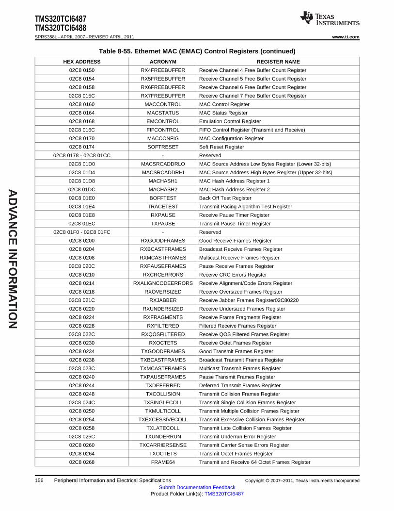
AD
VA
NC
E IN
FO
RM
AT
ION
TMS320TCI6487TMS320TCI6488SPRS358L–APRIL 2007–REVISED APRIL 2011 www.ti.com
Table 8-55. Ethernet MAC (EMAC) Control Registers (continued)
HEX ADDRESS ACRONYM REGISTER NAME
02C8 0150 RX4FREEBUFFER Receive Channel 4 Free Buffer Count Register
02C8 0154 RX5FREEBUFFER Receive Channel 5 Free Buffer Count Register
02C8 0158 RX6FREEBUFFER Receive Channel 6 Free Buffer Count Register
02C8 015C RX7FREEBUFFER Receive Channel 7 Free Buffer Count Register
02C8 0160 MACCONTROL MAC Control Register
02C8 0164 MACSTATUS MAC Status Register
02C8 0168 EMCONTROL Emulation Control Register
02C8 016C FIFCONTROL FIFO Control Register (Transmit and Receive)
02C8 0170 MACCONFIG MAC Configuration Register
02C8 0174 SOFTRESET Soft Reset Register
02C8 0178 - 02C8 01CC - Reserved
02C8 01D0 MACSRCADDRLO MAC Source Address Low Bytes Register (Lower 32-bits)
02C8 01D4 MACSRCADDRHI MAC Source Address High Bytes Register (Upper 32-bits)
02C8 01D8 MACHASH1 MAC Hash Address Register 1
02C8 01DC MACHASH2 MAC Hash Address Register 2
02C8 01E0 BOFFTEST Back Off Test Register
02C8 01E4 TRACETEST Transmit Pacing Algorithm Test Register
02C8 01E8 RXPAUSE Receive Pause Timer Register
02C8 01EC TXPAUSE Transmit Pause Timer Register
02C8 01F0 - 02C8 01FC - Reserved
02C8 0200 RXGOODFRAMES Good Receive Frames Register
02C8 0204 RXBCASTFRAMES Broadcast Receive Frames Register
02C8 0208 RXMCASTFRAMES Multicast Receive Frames Register
02C8 020C RXPAUSEFRAMES Pause Receive Frames Register
02C8 0210 RXCRCERRORS Receive CRC Errors Register
02C8 0214 RXALIGNCODEERRORS Receive Alignment/Code Errors Register
02C8 0218 RXOVERSIZED Receive Oversized Frames Register
02C8 021C RXJABBER Receive Jabber Frames Register02C80220
02C8 0220 RXUNDERSIZED Receive Undersized Frames Register
02C8 0224 RXFRAGMENTS Receive Frame Fragments Register
02C8 0228 RXFILTERED Filtered Receive Frames Register
02C8 022C RXQOSFILTERED Receive QOS Filtered Frames Register
02C8 0230 RXOCTETS Receive Octet Frames Register
02C8 0234 TXGOODFRAMES Good Transmit Frames Register
02C8 0238 TXBCASTFRAMES Broadcast Transmit Frames Register
02C8 023C TXMCASTFRAMES Multicast Transmit Frames Register
02C8 0240 TXPAUSEFRAMES Pause Transmit Frames Register
02C8 0244 TXDEFERRED Deferred Transmit Frames Register
02C8 0248 TXCOLLISION Transmit Collision Frames Register
02C8 024C TXSINGLECOLL Transmit Single Collision Frames Register
02C8 0250 TXMULTICOLL Transmit Multiple Collision Frames Register
02C8 0254 TXEXCESSIVECOLL Transmit Excessive Collision Frames Register
02C8 0258 TXLATECOLL Transmit Late Collision Frames Register
02C8 025C TXUNDERRUN Transmit Underrun Error Register
02C8 0260 TXCARRIERSENSE Transmit Carrier Sense Errors Register
02C8 0264 TXOCTETS Transmit Octet Frames Register
02C8 0268 FRAME64 Transmit and Receive 64 Octet Frames Register
156 Peripheral Information and Electrical Specifications Copyright © 2007–2011, Texas Instruments Incorporated
Submit Documentation FeedbackProduct Folder Link(s): TMS320TCI6487

AD
VA
NC
E I
NF
OR
MA
TIO
N
TMS320TCI6487TMS320TCI6488
www.ti.com SPRS358L–APRIL 2007–REVISED APRIL 2011
Table 8-55. Ethernet MAC (EMAC) Control Registers (continued)
HEX ADDRESS ACRONYM REGISTER NAME
02C8 026C FRAME65T127 Transmit and Receive 65 to 127 Octet Frames Register
02C8 0270 FRAME128T255 Transmit and Receive 128 to 255 Octet Frames Register
02C8 0274 FRAME256T511 Transmit and Receive 256 to 511 Octet Frames Register
02C8 0278 FRAME512T1023 Transmit and Receive 512 to 1023 Octet Frames Register
02C8 027C FRAME1024TUP Transmit and Receive 1024 to 1518 Octet Frames Register
02C8 0280 NETOCTETS Network Octet Frames Register
02C8 0284 RXSOFOVERRUNS Receive FIFO or DMA Start of Frame Overruns Register
02C8 0288 RXMOFOVERRUNS Receive FIFO or DMA Middle of Frame Overruns Register
02C8 028C RXDMAOVERRUNS Receive DMA Start of Frame and Middle of Frame OverrunsRegister
02C8 0300 - 02C8 03FC - Reserved
02C8 0400 - 02C8 04FC - Reserved
02C8 0500 MACADDRLO MAC Address Low Bytes Register (used in Receive AddressMatching)
02C8 0504 MACADDRHI MAC Address High Bytes Register (used in Receive AddressMatching)
02C8 0508 MACINDEX MAC Index Register
02C8 050C - 02C8 05FC - Reserved
02C8 0600 TX0HDP Transmit Channel 0 DMA Head Descriptor Pointer Register
02C8 0604 TX1HDP Transmit Channel 1 DMA Head Descriptor Pointer Register
02C8 0608 TX2HDP Transmit Channel 2 DMA Head Descriptor Pointer Register
02C8 060C TX3HDP Transmit Channel 3 DMA Head Descriptor Pointer Register
02C8 0610 TX4HDP Transmit Channel 4 DMA Head Descriptor Pointer Register
02C8 0614 TX5HDP Transmit Channel 5 DMA Head Descriptor Pointer Register
02C8 0618 TX6HDP Transmit Channel 6 DMA Head Descriptor Pointer Register
02C8 061C TX7HDP Transmit Channel 7 DMA Head Descriptor Pointer Register
02C8 0620 RX0HDP Receive Channel 0 DMA Head Descriptor Pointer Register
02C8 0624 RX1HDP Receive t Channel 1 DMA Head Descriptor Pointer Register
02C8 0628 RX2HDP Receive Channel 2 DMA Head Descriptor Pointer Register
02C8 062C RX3HDP Receive t Channel 3 DMA Head Descriptor Pointer Register
02C8 0630 RX4HDP Receive Channel 4 DMA Head Descriptor Pointer Register
02C8 0634 RX5HDP Receive t Channel 5 DMA Head Descriptor Pointer Register
02C8 0638 RX6HDP Receive Channel 6 DMA Head Descriptor Pointer Register
02C8 063C RX7HDP Receive t Channel 7 DMA Head Descriptor Pointer Register
02C8 0640 TX0CP Transmit Channel 0 Completion Pointer (Interrupt Acknowledge)Register
02C8 0644 TX1CP Transmit Channel 1 Completion Pointer (Interrupt Acknowledge)Register
02C8 0648 TX2CP Transmit Channel 2 Completion Pointer (Interrupt Acknowledge)Register
02C8 064C TX3CP Transmit Channel 3 Completion Pointer (Interrupt Acknowledge)Register
02C8 0650 TX4CP Transmit Channel 4 Completion Pointer (Interrupt Acknowledge)Register
02C8 0654 TX5CP Transmit Channel 5 Completion Pointer (Interrupt Acknowledge)Register
02C8 0658 TX6CP Transmit Channel 6 Completion Pointer (Interrupt Acknowledge)Register
02C8 065C TX7CP Transmit Channel 7 Completion Pointer (Interrupt Acknowledge)Register
Copyright © 2007–2011, Texas Instruments Incorporated Peripheral Information and Electrical Specifications 157Submit Documentation Feedback
Product Folder Link(s): TMS320TCI6487

AD
VA
NC
E IN
FO
RM
AT
ION
TMS320TCI6487TMS320TCI6488SPRS358L–APRIL 2007–REVISED APRIL 2011 www.ti.com
Table 8-55. Ethernet MAC (EMAC) Control Registers (continued)
HEX ADDRESS ACRONYM REGISTER NAME
02C8 0660 RX0CP Receive Channel 0 Completion Pointer (Interrupt Acknowledge)Register
02C8 0664 RX1CP Receive Channel 1 Completion Pointer (Interrupt Acknowledge)Register
02C8 0668 RX2CP Receive Channel 2 Completion Pointer (Interrupt Acknowledge)Register
02C8 066C RX3CP Receive Channel 3 Completion Pointer (Interrupt Acknowledge)Register
02C8 0670 RX4CP Receive Channel 4 Completion Pointer (Interrupt Acknowledge)Register
02C8 0674 RX5CP Receive Channel 5 Completion Pointer (Interrupt Acknowledge)Register
02C8 0678 RX6CP Receive Channel 6 Completion Pointer (Interrupt Acknowledge)Register
02C8 067C RX7CP Receive Channel 7 Completion Pointer (Interrupt Acknowledge)Register
02C8 0680 - 02C8 06FC - Reserved
02C8 0700 - 02C8 077C - Reserved
02C8 0780 - 02C8 0FFF - Reserved
Table 8-56. EMAC Statistics Registers
HEX ADDRESS ACRONYM REGISTER NAME
02C8 0200 RXGOODFRAMES Good Receive Frames Register
02C8 0204 RXBCASTFRAMES Broadcast Receive Frames Register (Total number ofGood Broadcast Frames Receive)
02C8 0208 RXMCASTFRAMES Multicast Receive Frames Register (Total number of GoodMulticast Frames Received)
02C8 020C RXPAUSEFRAMES Pause Receive Frames Register
02C8 0210 RXCRCERRORS Receive CRC Errors Register (Total number of FramesReceived with CRC Errors)
02C8 0214 RXALIGNCODEERRORS Receive Alignment/Code Errors register (Total number offrames Received with alignment/code errors)
02C8 0218 RXOVERSIZED Receive Oversized Frames Register (Total number ofOversized Frames Received)
02C8 021C RXJABBER Receive Jabber Frames Register (Total number of JabberFrames Received)
02C8 0220 RXUNDERSIZED Receive Undersized Frames Register (Total number ofUndersized Frames Received)
02C8 0224 RXFRAGMENTS Receive Frame Fragments Register
02C8 0228 RXFILTERED Filtered Receive Frames Register
02C8 022C RXQOSFILTERERED Received QOS Filtered Frames Register
02C8 0230 RXOCTETS Receive Octet Frames Register (Total number ofReceived Bytes in Good Frames)
02C8 0234 TXGOODFRAMES Good Transmit Frames Register (Total number of GoodFrames Transmitted)
02C8 0238 TXBCASTFRAMES Broadcast Transmit Frames Register
02C8 023C TXMCASTFRAMES Multicast Transmit Frames Register
02C8 0240 TXPAUSEFRAMES Pause Transmit Frames Register
02C8 0244 TXDEFERED Deferred Transmit Frames Register
02C8 0248 TXCOLLISION Transmit Collision Frames Register
02C8 024C TXSINGLECOLL Transmit Single Collision Frames Register
02C8 0250 TXMULTICOLL Transmit Multiple Collision Frames Register
158 Peripheral Information and Electrical Specifications Copyright © 2007–2011, Texas Instruments Incorporated
Submit Documentation FeedbackProduct Folder Link(s): TMS320TCI6487
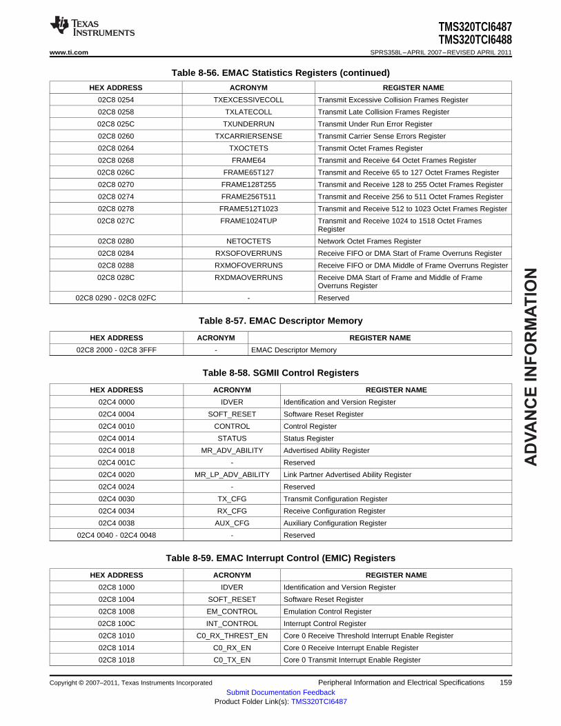
AD
VA
NC
E I
NF
OR
MA
TIO
N
TMS320TCI6487TMS320TCI6488
www.ti.com SPRS358L–APRIL 2007–REVISED APRIL 2011
Table 8-56. EMAC Statistics Registers (continued)
HEX ADDRESS ACRONYM REGISTER NAME
02C8 0254 TXEXCESSIVECOLL Transmit Excessive Collision Frames Register
02C8 0258 TXLATECOLL Transmit Late Collision Frames Register
02C8 025C TXUNDERRUN Transmit Under Run Error Register
02C8 0260 TXCARRIERSENSE Transmit Carrier Sense Errors Register
02C8 0264 TXOCTETS Transmit Octet Frames Register
02C8 0268 FRAME64 Transmit and Receive 64 Octet Frames Register
02C8 026C FRAME65T127 Transmit and Receive 65 to 127 Octet Frames Register
02C8 0270 FRAME128T255 Transmit and Receive 128 to 255 Octet Frames Register
02C8 0274 FRAME256T511 Transmit and Receive 256 to 511 Octet Frames Register
02C8 0278 FRAME512T1023 Transmit and Receive 512 to 1023 Octet Frames Register
02C8 027C FRAME1024TUP Transmit and Receive 1024 to 1518 Octet FramesRegister
02C8 0280 NETOCTETS Network Octet Frames Register
02C8 0284 RXSOFOVERRUNS Receive FIFO or DMA Start of Frame Overruns Register
02C8 0288 RXMOFOVERRUNS Receive FIFO or DMA Middle of Frame Overruns Register
02C8 028C RXDMAOVERRUNS Receive DMA Start of Frame and Middle of FrameOverruns Register
02C8 0290 - 02C8 02FC - Reserved
Table 8-57. EMAC Descriptor Memory
HEX ADDRESS ACRONYM REGISTER NAME
02C8 2000 - 02C8 3FFF - EMAC Descriptor Memory
Table 8-58. SGMII Control Registers
HEX ADDRESS ACRONYM REGISTER NAME
02C4 0000 IDVER Identification and Version Register
02C4 0004 SOFT_RESET Software Reset Register
02C4 0010 CONTROL Control Register
02C4 0014 STATUS Status Register
02C4 0018 MR_ADV_ABILITY Advertised Ability Register
02C4 001C - Reserved
02C4 0020 MR_LP_ADV_ABILITY Link Partner Advertised Ability Register
02C4 0024 - Reserved
02C4 0030 TX_CFG Transmit Configuration Register
02C4 0034 RX_CFG Receive Configuration Register
02C4 0038 AUX_CFG Auxiliary Configuration Register
02C4 0040 - 02C4 0048 - Reserved
Table 8-59. EMAC Interrupt Control (EMIC) Registers
HEX ADDRESS ACRONYM REGISTER NAME
02C8 1000 IDVER Identification and Version Register
02C8 1004 SOFT_RESET Software Reset Register
02C8 1008 EM_CONTROL Emulation Control Register
02C8 100C INT_CONTROL Interrupt Control Register
02C8 1010 C0_RX_THREST_EN Core 0 Receive Threshold Interrupt Enable Register
02C8 1014 C0_RX_EN Core 0 Receive Interrupt Enable Register
02C8 1018 C0_TX_EN Core 0 Transmit Interrupt Enable Register
Copyright © 2007–2011, Texas Instruments Incorporated Peripheral Information and Electrical Specifications 159Submit Documentation Feedback
Product Folder Link(s): TMS320TCI6487
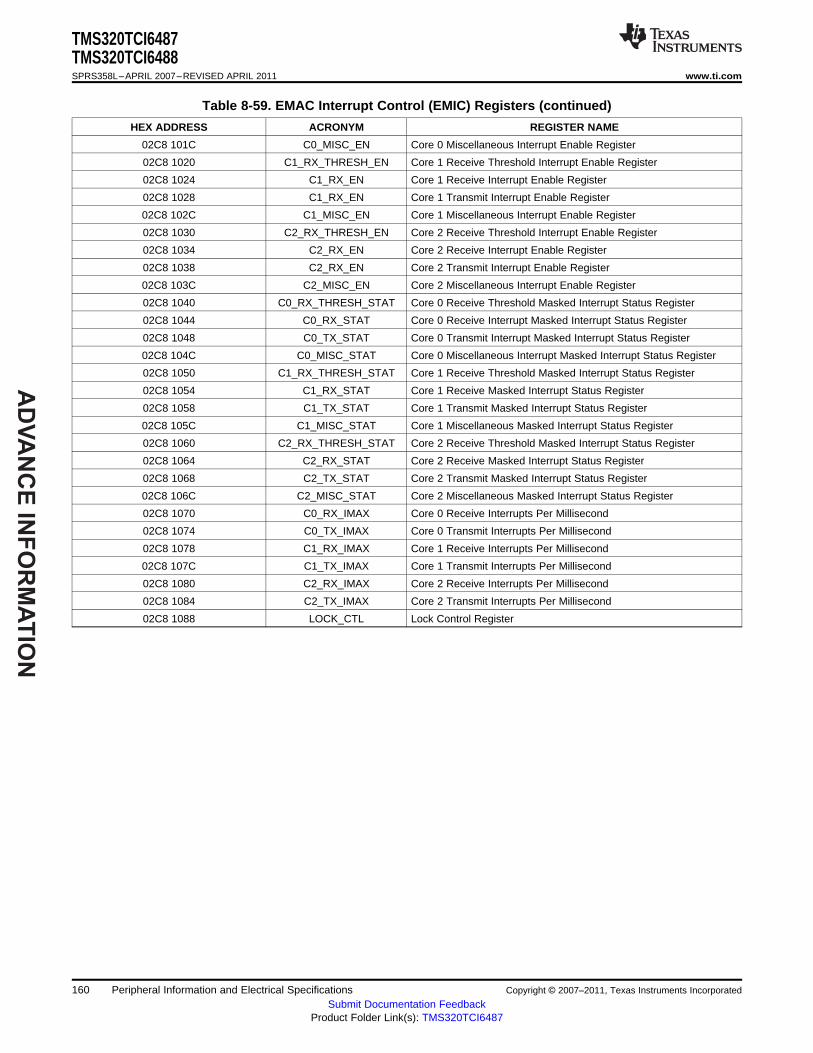
AD
VA
NC
E IN
FO
RM
AT
ION
TMS320TCI6487TMS320TCI6488SPRS358L–APRIL 2007–REVISED APRIL 2011 www.ti.com
Table 8-59. EMAC Interrupt Control (EMIC) Registers (continued)
HEX ADDRESS ACRONYM REGISTER NAME
02C8 101C C0_MISC_EN Core 0 Miscellaneous Interrupt Enable Register
02C8 1020 C1_RX_THRESH_EN Core 1 Receive Threshold Interrupt Enable Register
02C8 1024 C1_RX_EN Core 1 Receive Interrupt Enable Register
02C8 1028 C1_RX_EN Core 1 Transmit Interrupt Enable Register
02C8 102C C1_MISC_EN Core 1 Miscellaneous Interrupt Enable Register
02C8 1030 C2_RX_THRESH_EN Core 2 Receive Threshold Interrupt Enable Register
02C8 1034 C2_RX_EN Core 2 Receive Interrupt Enable Register
02C8 1038 C2_RX_EN Core 2 Transmit Interrupt Enable Register
02C8 103C C2_MISC_EN Core 2 Miscellaneous Interrupt Enable Register
02C8 1040 C0_RX_THRESH_STAT Core 0 Receive Threshold Masked Interrupt Status Register
02C8 1044 C0_RX_STAT Core 0 Receive Interrupt Masked Interrupt Status Register
02C8 1048 C0_TX_STAT Core 0 Transmit Interrupt Masked Interrupt Status Register
02C8 104C C0_MISC_STAT Core 0 Miscellaneous Interrupt Masked Interrupt Status Register
02C8 1050 C1_RX_THRESH_STAT Core 1 Receive Threshold Masked Interrupt Status Register
02C8 1054 C1_RX_STAT Core 1 Receive Masked Interrupt Status Register
02C8 1058 C1_TX_STAT Core 1 Transmit Masked Interrupt Status Register
02C8 105C C1_MISC_STAT Core 1 Miscellaneous Masked Interrupt Status Register
02C8 1060 C2_RX_THRESH_STAT Core 2 Receive Threshold Masked Interrupt Status Register
02C8 1064 C2_RX_STAT Core 2 Receive Masked Interrupt Status Register
02C8 1068 C2_TX_STAT Core 2 Transmit Masked Interrupt Status Register
02C8 106C C2_MISC_STAT Core 2 Miscellaneous Masked Interrupt Status Register
02C8 1070 C0_RX_IMAX Core 0 Receive Interrupts Per Millisecond
02C8 1074 C0_TX_IMAX Core 0 Transmit Interrupts Per Millisecond
02C8 1078 C1_RX_IMAX Core 1 Receive Interrupts Per Millisecond
02C8 107C C1_TX_IMAX Core 1 Transmit Interrupts Per Millisecond
02C8 1080 C2_RX_IMAX Core 2 Receive Interrupts Per Millisecond
02C8 1084 C2_TX_IMAX Core 2 Transmit Interrupts Per Millisecond
02C8 1088 LOCK_CTL Lock Control Register
160 Peripheral Information and Electrical Specifications Copyright © 2007–2011, Texas Instruments Incorporated
Submit Documentation FeedbackProduct Folder Link(s): TMS320TCI6487

AD
VA
NC
E I
NF
OR
MA
TIO
N
2
1
3
4
4
SRIOSGMIIREFCLK(N|P)
TMS320TCI6487TMS320TCI6488
www.ti.com SPRS358L–APRIL 2007–REVISED APRIL 2011
8.13.3 EMAC Electrical Data/Timing (SGMII)
The TMS320TCI6487/88 Hardware Design Guide application report (literature numberSPRAAG5 ) specifies a complete EMAC anc SGMII interface solutions for the TCI6487/8device as well as a list of compatible EMAC and SGMII devices. TI has performed the simulation andsystem characterization to ensure all EMAC and SGMII interface timings in this solution are met.
TI only supports designs that follow the board design guidelines outlined in the SPRAAG5application report.
Table 8-60. Timing Requirements for SRIOSGMIIREFCLK(N|P) (1)
(see Figure 8-35)
NO. PARAMETERS MIN MAX UNIT
1 tc(SRIOSGMIIREFCLK) Cycle time, SRIOSGMIIREFCLK(N|P) 3.2 8 ns
2 tw(CLKH) Pulse duration, CLK(N|P) high 0.4C ns
3 tw(CLKL) Pulse duration, CLK(N|P) low 0.4C ns
4 tt(CLK) Transition time, CLK(N|P) 50 1300 ps
5 tj(CLK) Period Jitter (RMS), CLK(N|P) 4 ps
(1) C=1/SRIOSGMIIREFCLK(N|P)
Figure 8-35. SRIOSGMIIREFCLK(N|P) Timing
Copyright © 2007–2011, Texas Instruments Incorporated Peripheral Information and Electrical Specifications 161Submit Documentation Feedback
Product Folder Link(s): TMS320TCI6487
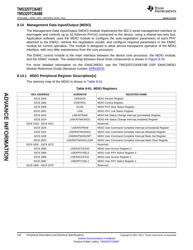
AD
VA
NC
E IN
FO
RM
AT
ION
TMS320TCI6487TMS320TCI6488SPRS358L–APRIL 2007–REVISED APRIL 2011 www.ti.com
8.14 Management Data Input/Output (MDIO)
The Management Data Input/Output (MDIO) module implements the 802.3 serial management interface tointerrogate and controls up to 32 Ethernet PHY(s) connected to the device, using a shared two-wire bus.Application software uses the MDIO module to configure the auto-negotiation parameters of each PHYattached to the EMAC, retrieve the negotiation results, and configure required parameters in the EMACmodule for correct operation. The module is designed to allow almost transparent operation of the MDIOinterface, with very little maintenance from the core processor.
The EMAC control module is the main interface between the device core processor, the MDIO module,and the EMAC module. The relationship between these three components is shown in Figure 8-34.
For more detailed information on the EMAC/MDIO, see the TMS320TCI6487/88 DSP EMAC/MDIOModule Reference Guide (literature number SPRUEF0).
8.14.1 MDIO Peripheral Register Description(s)
The memory map of the MDIO is shown in Table 8-61.
Table 8-61. MDIO Registers
HEX ADDRESS ACRONYM REGISTER NAME
02C8 1800 VERSION MDIO Version Register
02C8 1804 CONTROL MDIO Control Register
02C8 1808 ALIVE MDIO PHY Alive Status Register
02C8 180C LINK MDIO PHY Link Status Register
02C8 1810 LINKINTRAW MDIO link Status Change Interrupt (unmasked) Register
02C8 1814 LINKINTMASKED MDIO link Status Change Interrupt (masked) Register
02C8 1818 - 02C8 181C - Reserved
02C8 1820 USERINTRAW MDIO User Command Complete Interrupt (Unmasked) Register
02C8 1824 USERINTMASKED MDIO User Command Complete Interrupt (Masked) Register
02C8 1828 USERINTMASKSET MDIO User Command Complete Interrupt Mask Set Register
02C8 182C USERINTMASKCLEAR MDIO User Command Complete Interrupt Mask Clear Register
02C8 1830 - 02C8 187C - Reserved
02C8 1880 USERACCESS0 MDIO User Access Register 0
02C8 1884 USERPHYSEL0 MDIO User PHY Select Register 0
02C8 1888 USERACCESS1 MDIO User Access Register 1
02C8 188C USERPHYSEL1 MDIO User PHY Select Register 1
02C8 1890 - 02C8 1FFF - Reserved
162 Peripheral Information and Electrical Specifications Copyright © 2007–2011, Texas Instruments Incorporated
Submit Documentation FeedbackProduct Folder Link(s): TMS320TCI6487

AD
VA
NC
E I
NF
OR
MA
TIO
N
MDCLK
MDIO(input)
5
4
1
MDCLK
MDIO(input)
7
1
TMS320TCI6487TMS320TCI6488
www.ti.com SPRS358L–APRIL 2007–REVISED APRIL 2011
8.14.2 MDIO Electrical Data/Timing
Table 8-62. Timing Requirements for MDIO Inputs(see Figure 8-36)
NO. MIN MAX UNIT
1 tc(MDCLK) Cycle time, MDCLK 400 ns
2a tw(MDCLK) Pulse duration, MDCLK high 180 ns
2b tw(MDCLK) Pulse duration, MDCLK low 180 ns
3 tt(MDCLK) Transition time, MDCLK 5 ns
4 tsu(MDIO-MDCLKH) Setup time, MDIO data input valid before MDCLK high 10 ns
5 th(MDCLKH-MDIO) Hold time, MDIO data input valid after MDCLK high 10 ns
Figure 8-36. MDIO Input Timing
Table 8-63. Switching Characteristics Over Recommended Operating Conditions for MDIO Outputs(see Figure 8-37)
NO. MIN MAX UNIT
7 td(MDCLKL-MDIO) Delay time, MDCLK low to MDIO data output valid 100 ns
Figure 8-37. MDIO Output Timing
Copyright © 2007–2011, Texas Instruments Incorporated Peripheral Information and Electrical Specifications 163Submit Documentation Feedback
Product Folder Link(s): TMS320TCI6487
AD
VA
NC
E IN
FO
RM
AT
ION
TMS320TCI6487TMS320TCI6488SPRS358L–APRIL 2007–REVISED APRIL 2011 www.ti.com
8.15 Timers
The timers can be used to: time events, count events, generate pulses, interrupt the CPU, and sendsynchronization event so the EDMA3 channel controller.
8.15.1 Timers Device-Specific Information
The device has six general purpose timers: Timer0 to Timer5, each of which can be configured as ageneral purpose timer or a watchdog timer. When configured as a general-purpose timer, each timer canbe programmed as a 64-bit timer or as two separate 32-bit timers.
Each timer is made up of two 32-bit counters: a high counter and a low counter. The timer pinout isdescribed in the next section.
8.15.1.1 Timer I/O Selection
Not all timer inputs and outputs are pinned out of the device. The six timers have a flexible (e.g. softwarecontrolled) selection of timer inputs and outputs. At the chip level there are four timer pins, two input pins(TIMI[1:0]) and two output pins (TIMO[1:0]). Each timer input can be configured to be driven by either ofthe timer input pins, or by an FSYNC event (FSEVT[3:2]). Each output pin can be driven by any of thetimer outputs. This is programmable through software via the Timer Pin Manager Block, as shown in theFigure 8-38. Not shown in the figure is the logic that gates the timer resets that are routed to the PLLcontroller, shown in Figure 8-39.
164 Peripheral Information and Electrical Specifications Copyright © 2007–2011, Texas Instruments Incorporated
Submit Documentation FeedbackProduct Folder Link(s): TMS320TCI6487

AD
VA
NC
E I
NF
OR
MA
TIO
N
10 2 3
10 2 3
10 2 3
10 2 3
10 2 3
10 2 3
10 2 3
10 2 3
10 2 3
10 2 3
10 2 3
10 2 3
0 1 2 3 4 5 6 7 8 91011
0 1 2 3 4 5 6 7 8 91011
TO
UT
L
TO
UT
H
TIN
PL
TIN
PH
Timer645
TO
UT
L
TO
UT
H
TIN
PL
TIN
PH
Timer644
TO
UT
L
TO
UT
H
TIN
PL
TIN
PH
Timer643
TO
UT
L
TO
UT
H
TIN
PL
TIN
PH
Timer6422
TO
UT
L
TO
UT
H
TIN
PL
TIN
PH
Timer641
TO
UT
L
TO
UT
H
TIN
PL
TIN
PH
Timer640
FSEVT2
FSEVT3
TINPHSEL 0
TINPLSEL 0
TINPHSEL 1
TINPLSEL 1
TINPHSEL 2
TINPLSEL 2
TINPHSEL 3
TINPLSEL 3
TINPHSEL 4
TINPLSEL 4
TINPHSEL 5
TINPLSEL 5
TOUTSEL 1
TOUTSEL 0
32CFG SCR(SCR F)
TIMI0 TIMI1 TIMO0 TIMO1
vbusp
Timer Pin Manager(TPMGR)
SYSCLK/6
TMS320TCI6487TMS320TCI6488
www.ti.com SPRS358L–APRIL 2007–REVISED APRIL 2011
Figure 8-38. Timer Manager Block Diagram
Note that the TMS320C6472/TMS320TCI648x DSP 64-Bit Timer User’s Guide (literature numberSPRU818) uses different labels for its inputs and outputs. To avoid confusion with respect to numbering, adifferent convention is used in this document, as shown in Table 8-64.
Table 8-64. Timer Pin Naming
TIMER SIGNAL NAME RENAMED TO DESCRIPTION
n TINP12 TINPLn Timer n input event (low half). Used to drive lower 32-bit timer, 64-bit timer.Used in watchdog mode.
n TINP34 TINPHn Timer n input event (high half). Used to drive upper 32-bit timer. Unused in64-bit or watchdog modes.
n TOUT12 TOUTLn Timer n output (low half). Driven by lower 32-bit timer, 64-bit timer, orwatchdog timer as either a pulse or waveform.
n TOUT34 TOUTHn Timer n output (high half). Driven by upper 32-bit timer as either a pulse orwaveform. Unused in 64-bit or watchdog modes.
8.15.1.1.1 Timer Input Selection Register (TINPSEL)
Timer input selection is handled in the Timer input selection register (TINPSEL). The TINPSEL register isshown in Figure 8-39 and described in Table 8-65.
Copyright © 2007–2011, Texas Instruments Incorporated Peripheral Information and Electrical Specifications 165Submit Documentation Feedback
Product Folder Link(s): TMS320TCI6487

AD
VA
NC
E IN
FO
RM
AT
ION
TMS320TCI6487TMS320TCI6488SPRS358L–APRIL 2007–REVISED APRIL 2011 www.ti.com
31 24 23 22 21 20 19 18 17 16
Reserved TINPHSEL5 TINPLSEL5 TINPHSEL4 TINPLSEL4
R-00000000 R/W-01 R/W-00 R/W-01 R/W-00
15 14 13 12 11 10 9 8 7 6 5 4 3 2 1 0
TINPHSEL3 TINPLSEL3 TINPHSEL2 TINPLSEL2 TINPHSEL1 TINPLSEL1 TINPHSEL0 TINPLSEL0
R/W-01 R/W-00 R/W-01 R/W-00 R/W-01 R/W-00 R/W-01 R/W-00
LEGEND: R/W = Read/Write; R = Read only; -n = value after reset
Figure 8-39. Timer Input Selection Register (TINPSEL)
Table 8-65. Timer Input Selection Register (TINPSEL) Field Descriptions
Bit Field Value Description
31-24 Reserved Reserved
23:22 TINPHSEL5 Input Select for TIMER 5 High
00 TIMI0
01 TIMI1
10 FSEVT2
11 FSEVT3
21:20 TINPLSEL5 Input Select for TIMER 5 Low
00 TIMI0
01 TIMI1
10 FSEVT2
11 FSEVT3
19:18 TINPHSEL4 Input Select for TIMER 4 High
00 TIMI0
01 TIMI1
10 FSEVT2
11 FSEVT3
17:16 TINPLSEL4 Input Select for TIMER 4 Low
00 TIMI0
01 TIMI1
10 FSEVT2
11 FSEVT3
15:14 TINPHSEL3 Input Select for TIMER 3 High
00 TIMI0
01 TIMI1
10 FSEVT2
11 FSEVT3
13:12 TINPLSEL3 Input Select for TIMER 3 Low
00 TIMI0
01 TIMI1
10 FSEVT2
11 FSEVT3
11:10 TINPHSEL2 Input Select for TIMER 2 High
00 TIMI0
01 TIMI1
10 FSEVT2
11 FSEVT3
166 Peripheral Information and Electrical Specifications Copyright © 2007–2011, Texas Instruments Incorporated
Submit Documentation FeedbackProduct Folder Link(s): TMS320TCI6487

AD
VA
NC
E I
NF
OR
MA
TIO
N
TMS320TCI6487TMS320TCI6488
www.ti.com SPRS358L–APRIL 2007–REVISED APRIL 2011
Table 8-65. Timer Input Selection Register (TINPSEL) Field Descriptions (continued)
Bit Field Value Description
9:8 TINPLSEL2 Input Select for TIMER 2 Low
00 TIMI0
01 TIMI1
10 FSEVT2
11 FSEVT3
7:6 TINPHSEL1 Input Select for TIMER 1 High
00 TIMI0
01 TIMI1
10 FSEVT2
11 FSEVT3
5:4 TINPLSEL1 Input Select for TIMER 1 Low
00 TIMI0
01 TIMI1
10 FSEVT2
11 FSEVT3
3:2 TINPHSEL0 Input Select for TIMER 0 High
00 TIMI0
01 TIMI1
10 FSEVT2
11 FSEVT3
1:0 TINPLSEL0 Input Select for TIMER 0 Low
00 TIMI0
01 TIMI1
10 FSEVT2
11 FSEVT3
Copyright © 2007–2011, Texas Instruments Incorporated Peripheral Information and Electrical Specifications 167Submit Documentation Feedback
Product Folder Link(s): TMS320TCI6487

AD
VA
NC
E IN
FO
RM
AT
ION
TMS320TCI6487TMS320TCI6488SPRS358L–APRIL 2007–REVISED APRIL 2011 www.ti.com
8.15.1.1.2 Timer Output Selection Register (TOUTPSEL)
The timer output selection is handled in the Timer output selection register (TOUTPSEL). The TOUTPSELregister is shown in Figure 8-40 and described in Table 8-66.
31 16
Reserved
R-000000000000000000000000
15 8 7 4 3 0
Reserved TOUTPSEL1 TOUTPSEL0
R-000000000000000000000000 R/W-0001 R/W-0000
LEGEND: R/W = Read/Write; R = Read only; -n = value after reset
Figure 8-40. Timer Output Selection Register (TOUTPSEL)
Table 8-66. Timer Output Selection Register (TOUTPSEL) Field Descriptions
Bit Field Value Description
31:8 Reserved Reserved
7:4 TOUTPSEL1 Output Select for TIMI1
0000 TOUTL0
0001 TOUTH0
0010 TOUTL1
0011 TOUTH1
0100 TOUTL2
0101 TOUTH2
0110 TOUTL3
0111 TOUTH3
1000 TOUTL4
1001 TOUTH5
1010 TOUTL5
1011 TOUTH5
Other Reserved
3:0 TOUTPSEL0 Output Select for TIMO0
0000 TOUTL0
0001 TOUTH0
0010 TOUTL1
0011 TOUTH1
0100 TOUTL2
0101 TOUTH2
0110 TOUTL3
0111 TOUTH3
1000 TOUTL4
1001 TOUTH5
1010 TOUTL5
1011 TOUTH5
Other Reserved
168 Peripheral Information and Electrical Specifications Copyright © 2007–2011, Texas Instruments Incorporated
Submit Documentation FeedbackProduct Folder Link(s): TMS320TCI6487

AD
VA
NC
E I
NF
OR
MA
TIO
N
TMS320TCI6487TMS320TCI6488
www.ti.com SPRS358L–APRIL 2007–REVISED APRIL 2011
8.15.1.2 Timer Watchdog Select
As mentioned previously, the timers can operate in watchdog mode. When in watchdog mode, the eventoutput from the timer can optionally reset the CPU. When used in this type of mode, Timer3, Timer4, andTimer 5 correspond to C64x+ Megamodule Core 0, C64x+ Megamodule Core 1, and C64x+ MegamoduleCore 2, respectively. In order for the event not to trigger the reset when this operation is not desired, theTimer watchdog reset selection register (WDRSTSEL) is created to turn this feature on/off. TheWDRSTSEL register is shown in Figure 8-41 and described in Table 8-67.
31 8
Reserved
R-0 0000 0000 0000 0000 0000 0000 0000
7 3 2 1 0
Reserved WDRSTSEL5 WDRSTSEL4 WDRSTSEL3
R-0 0000 0000 0000 0000 0000 0000 0000 R/W-0 R/W-0 R/W-0
LEGEND: R/W = Read/Write; R = Read only; -n = value after reset
Figure 8-41. Timer Watchdog Reset Selection Register (WDRSTSEL)
Table 8-67. Timer Watchdog Reset Selection Register (WDRSTSEL) Field Descriptions
Bit Field Value Description
31:3 Reserved Reserved
2:2 WRDSTSELn Reset Select for Watchdog Timer
0 TOUTnL does not cause WDRSTSEL to assert to the corresponding C64x+ megamodule
1 TOUTnL causes a reset of the corresponding C64x+ megamodule via the host reset port of theLPSC
8.15.2 Timers Peripheral Description(s)
Table 8-68. Timer 0 Registers
HEX ADDRESS ACRONYM REGISTER NAME
0291 0000 PID Peripheral ID Register
0291 0004 EMUMGT_CLKSPD Timer 0 Emulation Management/Clock Speed Register
0291 0008 - Reserved
0291 000C - Reserved
0291 0010 TIMLO Timer 0 Counter Register Low
0291 0014 TIMHI Timer 0 Counter Register High
0291 0018 PRDLO Timer 0 Period Register Low
0291 001C PRDHI Timer 0 Period Register High
0291 0020 TCR Timer 0 Control Register
0291 0024 TGCR Timer 0 Global Control Register
0291 0028 WDTCR Timer 0 Watchdog Timer Control Register
0291 002C - Reserved
0291 0030 - Reserved
0291 0034 - 0291 FFFF - Reserved
Copyright © 2007–2011, Texas Instruments Incorporated Peripheral Information and Electrical Specifications 169Submit Documentation Feedback
Product Folder Link(s): TMS320TCI6487
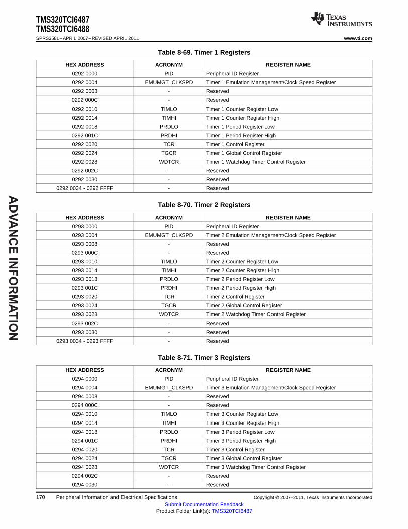
AD
VA
NC
E IN
FO
RM
AT
ION
TMS320TCI6487TMS320TCI6488SPRS358L–APRIL 2007–REVISED APRIL 2011 www.ti.com
Table 8-69. Timer 1 Registers
HEX ADDRESS ACRONYM REGISTER NAME
0292 0000 PID Peripheral ID Register
0292 0004 EMUMGT_CLKSPD Timer 1 Emulation Management/Clock Speed Register
0292 0008 - Reserved
0292 000C - Reserved
0292 0010 TIMLO Timer 1 Counter Register Low
0292 0014 TIMHI Timer 1 Counter Register High
0292 0018 PRDLO Timer 1 Period Register Low
0292 001C PRDHI Timer 1 Period Register High
0292 0020 TCR Timer 1 Control Register
0292 0024 TGCR Timer 1 Global Control Register
0292 0028 WDTCR Timer 1 Watchdog Timer Control Register
0292 002C - Reserved
0292 0030 - Reserved
0292 0034 - 0292 FFFF - Reserved
Table 8-70. Timer 2 Registers
HEX ADDRESS ACRONYM REGISTER NAME
0293 0000 PID Peripheral ID Register
0293 0004 EMUMGT_CLKSPD Timer 2 Emulation Management/Clock Speed Register
0293 0008 - Reserved
0293 000C - Reserved
0293 0010 TIMLO Timer 2 Counter Register Low
0293 0014 TIMHI Timer 2 Counter Register High
0293 0018 PRDLO Timer 2 Period Register Low
0293 001C PRDHI Timer 2 Period Register High
0293 0020 TCR Timer 2 Control Register
0293 0024 TGCR Timer 2 Global Control Register
0293 0028 WDTCR Timer 2 Watchdog Timer Control Register
0293 002C - Reserved
0293 0030 - Reserved
0293 0034 - 0293 FFFF - Reserved
Table 8-71. Timer 3 Registers
HEX ADDRESS ACRONYM REGISTER NAME
0294 0000 PID Peripheral ID Register
0294 0004 EMUMGT_CLKSPD Timer 3 Emulation Management/Clock Speed Register
0294 0008 - Reserved
0294 000C - Reserved
0294 0010 TIMLO Timer 3 Counter Register Low
0294 0014 TIMHI Timer 3 Counter Register High
0294 0018 PRDLO Timer 3 Period Register Low
0294 001C PRDHI Timer 3 Period Register High
0294 0020 TCR Timer 3 Control Register
0294 0024 TGCR Timer 3 Global Control Register
0294 0028 WDTCR Timer 3 Watchdog Timer Control Register
0294 002C - Reserved
0294 0030 - Reserved
170 Peripheral Information and Electrical Specifications Copyright © 2007–2011, Texas Instruments Incorporated
Submit Documentation FeedbackProduct Folder Link(s): TMS320TCI6487

AD
VA
NC
E I
NF
OR
MA
TIO
N
TMS320TCI6487TMS320TCI6488
www.ti.com SPRS358L–APRIL 2007–REVISED APRIL 2011
Table 8-71. Timer 3 Registers (continued)
HEX ADDRESS ACRONYM REGISTER NAME
0294 0034 - 0294 FFFF - Reserved
Table 8-72. Timer 4 Registers
HEX ADDRESS ACRONYM REGISTER NAME
0295 0000 PID Peripheral ID Register
0295 0004 EMUMGT_CLKSPD Timer 4 Emulation Management/Clock Speed Register
0295 0008 - Reserved
0295 000C - Reserved
0295 0010 TIMLO Timer 4 Counter Register Low
0295 0014 TIMHI Timer 4 Counter Register High
0295 0018 PRDLO Timer 4 Period Register Low
0295 001C PRDHI Timer 4 Period Register High
0295 0020 TCR Timer 4 Control Register
0295 0024 TGCR Timer 4 Global Control Register
0295 0028 WDTCR Timer 4 Watchdog Timer Control Register
0295 002C - Reserved
0295 0030 - Reserved
0295 0034 - 0295 FFFF - Reserved
Table 8-73. Timer 5 Registers
HEX ADDRESS ACRONYM REGISTER NAME
0296 0000 PID Peripheral ID Register
0296 0004 EMUMGT_CLKSPD Timer 5 Emulation Management/Clock Speed Register
0296 0008 - Reserved
0296 000C - Reserved
0296 0010 TIMLO Timer 5 Counter Register Low
0296 0014 TIMHI Timer 5 Counter Register High
0296 0018 PRDLO Timer 5 Period Register Low
0296 001C PRDHI Timer 5 Period Register High
0296 0020 TCR Timer 5 Control Register
0296 0024 TGCR Timer 5 Global Control Register
0296 0028 WDTCR Timer 5 Watchdog Timer Control Register
0296 002C - Reserved
0296 0030 - Reserved
0296 0034 - 0296 FFFF - Reserved
Table 8-74. Timer Device-Specific Registers
HEX ADDRESS ACRONYM REGISTER NAME
0290 0000 TINPSEL Timer Input Selection
0290 0004 TOUTPSEL Timer Output Selection
0290 0008 WDRSTSEL Watchdog Timer Reset Select
Copyright © 2007–2011, Texas Instruments Incorporated Peripheral Information and Electrical Specifications 171Submit Documentation Feedback
Product Folder Link(s): TMS320TCI6487

AD
VA
NC
E IN
FO
RM
AT
ION
TMS320TCI6487TMS320TCI6488SPRS358L–APRIL 2007–REVISED APRIL 2011 www.ti.com
8.15.3 Timers Electrical Data/Timing
Table 8-75. Timing Requirements for Timer Inputs (1)
(see Figure 8-42)
NO. PARAMETER MIN MAX UNIT
1 tw(TIMH) Pulse duration, TIMI high 12C ns
2 tw(TIMIL) Pulse duration, TIMI low 12C ns
(1) C = 1/CPU Clock, in ns.
Table 8-76. Switching Characteristics Over Recommended Operating Conditions for Timer Outputs (1)
(see Figure 8-42)
NO. PARAMETER MIN MAX UNIT
3 tw(TIMOH) Pulse duration, TIMO high 12C - 3 ns
4 tw(TIMOL) Pulse duration, TIMO low 12C - 3 ns
(1) If CORECLKSEL = 0, C = 1/SYSCLK(NIP) frequency, in ns. If CORECLKSEL = 1, C = 1/ALTCORECLK (N|P) frequency, in ns.
Figure 8-42. Timer Timing
172 Peripheral Information and Electrical Specifications Copyright © 2007–2011, Texas Instruments Incorporated
Submit Documentation FeedbackProduct Folder Link(s): TMS320TCI6487

AD
VA
NC
E I
NF
OR
MA
TIO
N
TMS320TCI6487TMS320TCI6488
www.ti.com SPRS358L–APRIL 2007–REVISED APRIL 2011
8.16 Enhanced Viterbi-Decoder Coprocessor (VCP2)
8.16.1 VCP2 Device-Specific Information
The TCI6487/8 device has a high-performance embedded coprocessor Viterbi-Decoder Coprocessor(VCP2) that significantly speeds up channel-decoding operations on-chip. The VCP2 operating at CPUclock divided-by-3 can decode over 694 7.95-Kbps adaptive multi-rate (AMR)(K = 9, R = 1/3) voicechannels. The VCP2 supports constraint lengths K = 5, 6, 7, 8, and 9, rates R = 3/4, 1/2, 1/3, 1/4, and 1/5,and flexible polynomials, while generating hard decisions or soft decisions. Communications between theVCP2 and the CPU are carried out through the EDMA3 controller.
The VCP2 supports:• Unlimited frame sizes• Code rates 3/4, 1/2, 1/3, 1/4, and 1/5• Constraint lengths 5, 6, 7, 8, and 9• Programmable encoder polynomials• Programmable reliability and convergence lengths• Hard and soft decoded decisions• Tail and convergent modes• Yamamoto logic• Tail biting logic• Various input and output FIFO lengths
For more detailed information on the VCP2, see the TMS320TCI648x DSP Viterbi-Decoder Coprocessor 2(VCP2) Reference Guide (literature number SPRUE09).
Copyright © 2007–2011, Texas Instruments Incorporated Peripheral Information and Electrical Specifications 173Submit Documentation Feedback
Product Folder Link(s): TMS320TCI6487

AD
VA
NC
E IN
FO
RM
AT
ION
TMS320TCI6487TMS320TCI6488SPRS358L–APRIL 2007–REVISED APRIL 2011 www.ti.com
8.16.2 VCP2 Peripheral Register Description(s)
Table 8-77. VCP2 Registers
EDMA BUS HEX ADDRESS RANGE CONFIGURATION BUS HEX ACRONYM REGISTER NAMEADDRESS RANGE
5800 0000 - VCPIC0 VCP2 input configuration Register 0
5800 0004 - VCPIC1 VCP2 input configuration Register 1
5800 0008 - VCPIC2 VCP2 input configuration Register 2
5800 000C - VCPIC3 VCP2 input configuration Register 3
5800 0010 - VCPIC4 VCP2 input configuration Register 4
5800 0014 - VCPIC5 VCP2 Input Configuration Register 5
5800 0018 - 5800 0044 - - Reserved
5800 0048 - VCPOUT0 VCP2 output Register 0
5800 004C - VCPOUT1 VCP2 output Register 1
5800 0050 - 5800 007C - - Reserved
5800 0080 N/A VCPWBM VCP2 branch metrics write FIFORegister
5800 0084 - 5800 009C - - Reserved
5800 00C0 N/A VCPRDECS VCP2 decisions read FIFO Register
N/A 02B8 0018 VCPEXE VCP2 execution Register
N/A 02B8 0020 VCPEND VCP2 Endian mode Register
N/A 02B8 0040 VCPSTAT0 VCP2 Status Register 0
N/A 02B8 0044 VCPSTAT1 VCP2 Status Register 1
N/A 02B8 0050 VCPERR VCP2 error Register
- - - Reserved
N/A 02B8 0060 VCPEMU VCP2 emulation control Register
N/A 02B8 0064 - 02B9 FFFF - Reserved
5800 1000 - BM Branch metrics
5800 2000 - SM State metric
5800 3000 - TBHD Traceback hard decision
5800 6000 - TBSD Traceback soft decision
5800 F000 - IO Decoded bits
174 Peripheral Information and Electrical Specifications Copyright © 2007–2011, Texas Instruments Incorporated
Submit Documentation FeedbackProduct Folder Link(s): TMS320TCI6487

AD
VA
NC
E I
NF
OR
MA
TIO
N
TMS320TCI6487TMS320TCI6488
www.ti.com SPRS358L–APRIL 2007–REVISED APRIL 2011
8.17 Enhanced Turbo Decoder Coprocessor (TCP2)
8.17.1 TCP2 Device-Specific Information
The TCI6487/8 device has a high-performance embedded coprocessor Turbo-Decoder Coprocessor(TCP2) that significantly speeds up channel-decoding operations on-chip. The TCP2 operating at CPUclock divided-by-3 can decode up to fifty 384-Kbps or eight 2-Mbps turbo-encoded channels (assuming 6iterations). The TCP2 implements the max* log-map algorithm and is designed to support all polynomialsand rates required by Third-Generation Partnership Projects (3GPP and 3GPP2), with fully programmableframe length and turbo interleaver. Decoding parameters such as the number of iterations and stoppingcriteria are also programmable. Communications between the TCP2 and the CPU are carried out throughthe EDMA3 controller.
The TCP2 supports:• Parallel concatenated convolutional turbo decoding using the MAP algorithm• All turbo code rates greater than or equal to 1/5• 3GPP and CDMA2000 turbo encoder trellis• 3GPP and CDMA2000 block sizes in standalone mode• Larger block sizes in shared processing mode• Both max log MAP and log MAP decoding• Sliding windows algorithm with variable reliability and prolog lengths• The prolog reduction algorithm• Execution of a minimum and maximum number of iterations• The SNR stopping criteria algorithm• The CRC stopping criteria algorithm
For more detailed information on the TCP2, see the TMS320TCI648x DSP Turbo-Decoder Coprocessor 2(TCP2) Reference Guide (literature number SPRUE10).
8.17.2 TCP2 Peripheral Register Description(s)
Table 8-78. TCP2 Registers
EDMA BUS HEX ADDRESS RANGE CONFIGURATION BUS HEX ACRONYM REGISTER NAMEADDRESS RANGE
5000 0000 - TCPIC0 TCP2 Input Configuration Register 0
5000 0004 - TCPIC1 TCP2 Input Configuration Register 1
5000 0008 - TCPIC2 TCP2 Input Configuration Register 2
5000 000C - TCPIC3 TCP2 Input Configuration Register 3
5000 0010 - TCPIC4 TCP2 Input Configuration Register 4
5000 0014 - TCPIC5 TCP2 Input Configuration Register 5
5000 0018 - TCPIC6 TCP2 Input Configuration Register 6
5000 001C - TCPIC7 TCP2 Input Configuration Register 7
5000 0020 - TCPIC8 TCP2 Input Configuration Register 8
5000 0024 - TCPIC9 TCP2 Input Configuration Register 9
5000 0028 - TCPIC10 TCP2 Input Configuration Register 10
5000 002C - TCPIC11 TCP2 Input Configuration Register 11
5000 0030 - TCPIC12 TCP2 Input Configuration Register 12
5000 0034 - TCPIC13 TCP2 Input Configuration Register 13
5000 0038 - TCPIC14 TCP2 Input Configuration Register 14
5000 003C - TCPIC15 TCP2 Input Configuration Register 15
5000 0040 - TCPOUT0 TCP2 Output Parameters Register 0
5000 0044 - TCPOUT1 TCP2 Output Parameters Register 1
Copyright © 2007–2011, Texas Instruments Incorporated Peripheral Information and Electrical Specifications 175Submit Documentation Feedback
Product Folder Link(s): TMS320TCI6487
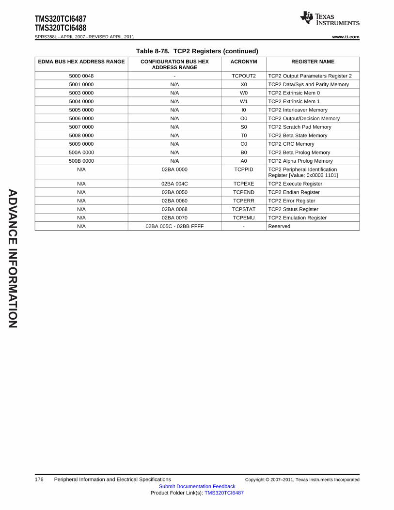
AD
VA
NC
E IN
FO
RM
AT
ION
TMS320TCI6487TMS320TCI6488SPRS358L–APRIL 2007–REVISED APRIL 2011 www.ti.com
Table 8-78. TCP2 Registers (continued)
EDMA BUS HEX ADDRESS RANGE CONFIGURATION BUS HEX ACRONYM REGISTER NAMEADDRESS RANGE
5000 0048 - TCPOUT2 TCP2 Output Parameters Register 2
5001 0000 N/A X0 TCP2 Data/Sys and Parity Memory
5003 0000 N/A W0 TCP2 Extrinsic Mem 0
5004 0000 N/A W1 TCP2 Extrinsic Mem 1
5005 0000 N/A I0 TCP2 Interleaver Memory
5006 0000 N/A O0 TCP2 Output/Decision Memory
5007 0000 N/A S0 TCP2 Scratch Pad Memory
5008 0000 N/A T0 TCP2 Beta State Memory
5009 0000 N/A C0 TCP2 CRC Memory
500A 0000 N/A B0 TCP2 Beta Prolog Memory
500B 0000 N/A A0 TCP2 Alpha Prolog Memory
N/A 02BA 0000 TCPPID TCP2 Peripheral IdentificationRegister [Value: 0x0002 1101]
N/A 02BA 004C TCPEXE TCP2 Execute Register
N/A 02BA 0050 TCPEND TCP2 Endian Register
N/A 02BA 0060 TCPERR TCP2 Error Register
N/A 02BA 0068 TCPSTAT TCP2 Status Register
N/A 02BA 0070 TCPEMU TCP2 Emulation Register
N/A 02BA 005C - 02BB FFFF - Reserved
176 Peripheral Information and Electrical Specifications Copyright © 2007–2011, Texas Instruments Incorporated
Submit Documentation FeedbackProduct Folder Link(s): TMS320TCI6487
AD
VA
NC
E I
NF
OR
MA
TIO
N
TMS320TCI6487TMS320TCI6488
www.ti.com SPRS358L–APRIL 2007–REVISED APRIL 2011
8.18 Serial RapidIO (SRIO) Port
The SRIO Port on the TCI6487/88 device is a high-performance, low pin-count interconnect aimed forembedded markets. The use of the RapidIO interconnect in a base band board design can create ahomogeneous interconnect environment, providing even more connectivity and control among thecomponents. RapidIO is based on the memory and device addressing concepts of processor buses wherethe transaction processing is managed completely by hardware. This enables the RapidIO interconnect tolower the system cost by providing lower latency, reduced overhead of packet data processing, and highersystem bandwidth, all of which are key for wireless interfaces. The RapidIO interconnect offers very lowpin-count interfaces with scalable system bandwidth based on 10-Gigabit per second (Gbps) bidirectionallinks.
The PHY part of the RIO consists of the physical layer and includes the input and output buffers (eachserial link consists of a differential pair), the 8-bit/10-bit encoder/decoder, the PLL clock recovery, and theparallel-to-serial/serial-to-parallel converters.
The RapidIO interface should be designed to operate at a data rate up to 3.125 Gbps per differential pair.
8.18.1 SRIO Device-Specific Information
The approach to specifying interface timing for the SRIO Port is different than on other interfaces such asMcBSP. For these other interfaces the device timing was specified in terms of data manual specificationsand I/O buffer information specification (IBIS) models.
For the SRIO Port, Texas Instruments (TI) provides a printed circuit board (PCB) solution showing twoDSPs connected via a 1x SRIO link directly to the user. TI has performed the simulation and systemcharacterization to ensure all SRIO interface timings in this solution are met. The complete SRIO systemsolution is documented in the TMS320TCI6487/88 DSP SERDES Implementation Guidelines applicationreport (literature number SPRAAG7).
TI only supports designs that follow the board design guidelines outlined in the SPRAAG7application report.
The Serial RapidIO peripheral is a master peripheral in the TCI6487/88 DSP. It conforms to the RapidIO™Interconnect Specification, Part VI: Physical Layer 1x/4x LP-Serial Specification, Revision 1.2.
8.18.2 SRIO Register Description(s)
Table 8-79. RapidIO Control Registers
HEX ADDRESS ACRONYM REGISTER NAME
02D0 0000 RIOPID RapidIO Peripheral Identification Register
02D0 0004 RIO_PCR RapidIO Peripheral Control Register
02D0 0008 - 02D0 001C - Reserved
02D0 0020 RIO_PER_SET_CNTL RapidIO Peripheral Settings Control Register
02D0 0024 - 02D0 002C - Reserved
02D0 0030 RIO_GBL_EN RapidIO Peripheral Global Enable Register
02D0 0034 RIO_GBL_EN_STAT RapidIO Peripheral Global Enable Status Register
02D0 0038 RIO_BLK0_EN RapidIO Block0 Enable Register
02D0 003C RIO_BLK0_EN_STAT RapidIO Block0 Enable Status Register
02D0 0040 RIO_BLK1_EN RapidIO Block1 Enable Register
02D0 0044 RIO_BLK1_EN_STAT RapidIO Block1 Enable Status Register
02D0 0048 RIO_BLK2_EN RapidIO Block2 Enable Register
02D0 004C RIO_BLK2_EN_STAT RapidIO Block2 Enable Status Register
02D0 0050 RIO_BLK3_EN RapidIO Block3 Enable Register
02D0 0054 RIO_BLK3_EN_STAT RapidIO Block3 Enable Status Register
02D0 0058 RIO_BLK4_EN RapidIO Block4 Enable Register
Copyright © 2007–2011, Texas Instruments Incorporated Peripheral Information and Electrical Specifications 177Submit Documentation Feedback
Product Folder Link(s): TMS320TCI6487
AD
VA
NC
E IN
FO
RM
AT
ION
TMS320TCI6487TMS320TCI6488SPRS358L–APRIL 2007–REVISED APRIL 2011 www.ti.com
Table 8-79. RapidIO Control Registers (continued)
HEX ADDRESS ACRONYM REGISTER NAME
02D0 005C RIO_BLK4_EN_STAT RapidIO Block4 Enable Status Register
02D0 0060 RIO_BLK5_EN RapidIO Block5 Enable Register
02D0 0064 RIO_BLK5_EN_STAT RapidIO Block5 Enable Status Register
02D0 0068 RIO_BLK6_EN RapidIO Block6 Enable Register
02D0 006C RIO_BLK6_EN_STAT RapidIO Block6 Enable Status Register
02D0 0070 RIO_BLK7_EN RapidIO Block7 Enable Register
02D0 0074 RIO_BLK7_EN_STAT RapidIO Block7 Enable Status Register
02D0 0078 RIO_BLK8_EN RapidIO Block8 Enable Register
02D0 007C RIO_BLK8_EN_STAT RapidIO Block8 Enable Status Register
02D0 0080 RIO_DEVICEID_REG1 RapidIO Device ID Register 1
02D0 0084 RIO_DEVICEID_REG2 RapidIO Device ID Register 2
02D0 0088 RIO_DEVICEID_REG3 RapidIO Device ID Register 3
02D0 008C RIO_DEVICEID_REG4 RapidIO Device ID Register 4
02D0 0090 PF_16B_CNTL0 Packet Forwarding Register 0 for 16-Bit Device IDs
02D0 0094 PF_8B_CNTL0 Packet Forwarding Register 0 for 8-Bit Device IDs
02D0 0098 PF_16B_CNTL1 Packet Forwarding Register 1 for 16-Bit Device IDs
02D0 009C PF_8B_CNTL1 Packet Forwarding Register 1 for 8-Bit Device IDs
02D0 00A0 PF_16B_CNTL2 Packet Forwarding Register 2 for 16-Bit Device IDs
02D0 00A4 PF_8B_CNTL2 Packet Forwarding Register 2 for 8-Bit Device IDs
02D0 00A8 PF_16B_CNTL3 Packet Forwarding Register 3 for 16-Bit Device IDs
02D0 00AC PF_8B_CNTL3 Packet Forwarding Register 3 for 8-Bit Device IDs
02D0 00B0 - 02D0 00FC - Reserved
02D0 0100 RIO_SERDES_CFGRX0_CNTL RapidIO SerDes RX Channel 0 CFG Register
02D0 0104 RIO_SERDES_CFGRX1_CNTL RapidIO SerDes RX Channel 1 CFG Register
02D0 0108 RIO_SERDES_CFGRX2_CNTL RapidIO SerDes RX Channel 2 CFG Register
02D0 010C RIO_SERDES_CFGRX3_CNTL RapidIO SerDes RX Channel 3 CFG Register
02D0 0110 RIO_SERDES_CFGTX0_CNTL RapidIO SerDes TX Channel 0 CFG Register
02D0 0114 RIO_SERDES_CFGTX1_CNTL RapidIO SerDes TX Channel 1 CFG Register
02D0 0118 RIO_SERDES_CFGTX2_CNTL RapidIO SerDes TX Channel 2 CFG Register
02D0 011C RIO_SERDES_CFGTX3_CNTL RapidIO SerDes TX Channel 3 CFG Register
02D0 0120 RIO_SERDS_CFG0_CNTL RapidIO SerDes Macro 0 CFG Control Register
02D0 0124 RIO_SERDS_CFG1_CNTL RapidIO SerDes Macro 1 CFG Control Register
02D0 0128 RIO_SERDS_CFG2_CNTL RapidIO SerDes Macro 2 CFG Control Register
02D0 012C RIO_SERDS_CFG3_CNTL RapidIO SerDes Macro 3 CFG Control Register
02D0 0130 - 02D0 01FC - Reserved
02D0 0200 DOORBELL0_ICSR DOORBELL Interrupt Condition Status Register 0
02D0 0204 - Reserved
02D0 0208 DOORBELL0_ICCR DOORBELL Interrupt Condition Clear Register 0
02D0 020C - Reserved
02D0 0210 DOORBELL1_ICSR DOORBELL Interrupt Condition Status Register 1
02D0 0214 - Reserved
02D0 0218 DOORBELL1_ICCR DOORBELL Interrupt Condition Clear Register 1
02D0 021C - Reserved
02D0 0220 DOORBELL2_ICSR DOORBELL Interrupt Condition Status Register 2
02D0 0224 - Reserved
02D0 0228 DOORBELL2_ICCR DOORBELL Interrupt Condition Clear Register 2
02D0 022C - Reserved
178 Peripheral Information and Electrical Specifications Copyright © 2007–2011, Texas Instruments Incorporated
Submit Documentation FeedbackProduct Folder Link(s): TMS320TCI6487
AD
VA
NC
E I
NF
OR
MA
TIO
N
TMS320TCI6487TMS320TCI6488
www.ti.com SPRS358L–APRIL 2007–REVISED APRIL 2011
Table 8-79. RapidIO Control Registers (continued)
HEX ADDRESS ACRONYM REGISTER NAME
02D0 0230 DOORBELL3_ICSR DOORBELL Interrupt Condition Status Register 3
02D0 0234 - Reserved
02D0 0238 DOORBELL3_ICCR DOORBELL Interrupt Condition Clear Register 3
02D0 023C - Reserved
02D0 0240 RX_CPPI_ICSR RX CPPI Interrupt Condition Status Register
02D0 0244 - Reserved
02D0 0248 RX_CPPI_ICCR RX CPPI Interrupt Condition Clear Register
02D0 024C - Reserved
02D0 0250 TX_CPPI_ICSR TX CPPI Interrupt Condition Status Register
02D0 0254 - Reserved
02D0 0258 TX_CPPI_ICCR TX CPPI Interrupt Condition Clear Register
02D0 025C - Reserved
02D0 0260 LSU_ICSR LSU Interrupt Condition Status Register
02D0 0264 - Reserved
02D0 0268 LSU_ICCR LSU Interrupt Condition Clear Register
02D0 026C - Reserved
02D0 0270 ERR_RST_EVNT_ICSR Error, Reset, and Special Event Interrupt Condition StatusRegister
02D0 0274 - Reserved
02D0 0278 ERR_RST_EVNT_ICCR Error, Reset, and Special Event Interrupt Condition ClearRegister
02D0 027C - Reserved
02D0 0280 DOORBELL0_ICRR DOORBELL0 Interrupt Condition Routing Register
02D0 0284 DOORBELL0_ICRR2 DOORBELL 0 Interrupt Condition Routing Register 2
02D0 0288 - 02D0 028C - Reserved
02D0 0290 DOORBELL1_ICRR DOORBELL1 Interrupt Condition Routing Register
02D0 0294 DOORBELL1_ICRR2 DOORBELL 1 Interrupt Condition Routing Register 2
02D0 0298 - 02D0 029C - Reserved
02D0 02A0 DOORBELL2_ICRR DOORBELL2 Interrupt Condition Routing Register
02D0 02A4 DOORBELL2_ICRR2 DOORBELL 2 Interrupt Condition Routing Register 2
02D0 02A8 - 02D0 02AC - Reserved
02D0 02B4 DOORBELL3_ICRR2 DOORBELL 3 Interrupt Condition Routing Register 2
02D0 02B8 - 02D0 02BC - Reserved
02D0 02C0 RX_CPPI _ICRR Receive CPPI Interrupt Condition Routing Register
02D0 02C4 RX_CPPI _ICRR2 Receive CPPI Interrupt Condition Routing Register 2
02D0 02C8 - 02D0 02CC - Reserved
02D0 02D0 TX_CPPI _ICRR Transmit CPPI Interrupt Condition Routing Register
02D0 02D4 TX_CPPI _ICRR2 Transmit CPPI Interrupt Condition Routing Register 2
02D0 02D8 - 02D0 02DC - Reserved
02D0 02E0 LSU_ICRR0 LSU Interrupt Condition Routing Register 0
02D0 02E4 LSU_ICRR1 LSU Interrupt Condition Routing Register 1
02D0 02E8 LSU_ICRR2 LSU Interrupt Condition Routing Register 2
02D0 02EC LSU_ICRR3 LSU Interrupt Condition Routing Register 3
02D0 02F0 ERR_RST_EVNT_ICRR Error, Reset, and Special Event Interrupt ConditionRouting Register
02D0 02F4 ERR_RST_EVNT_ICRR2 Error, Reset, and Special Event Interrupt ConditionRouting Register 2
02D0 02F8 ERR_RST_EVNT_ICRR3 Error, Reset, and Special Event Interrupt ConditionRouting Register 3
Copyright © 2007–2011, Texas Instruments Incorporated Peripheral Information and Electrical Specifications 179Submit Documentation Feedback
Product Folder Link(s): TMS320TCI6487
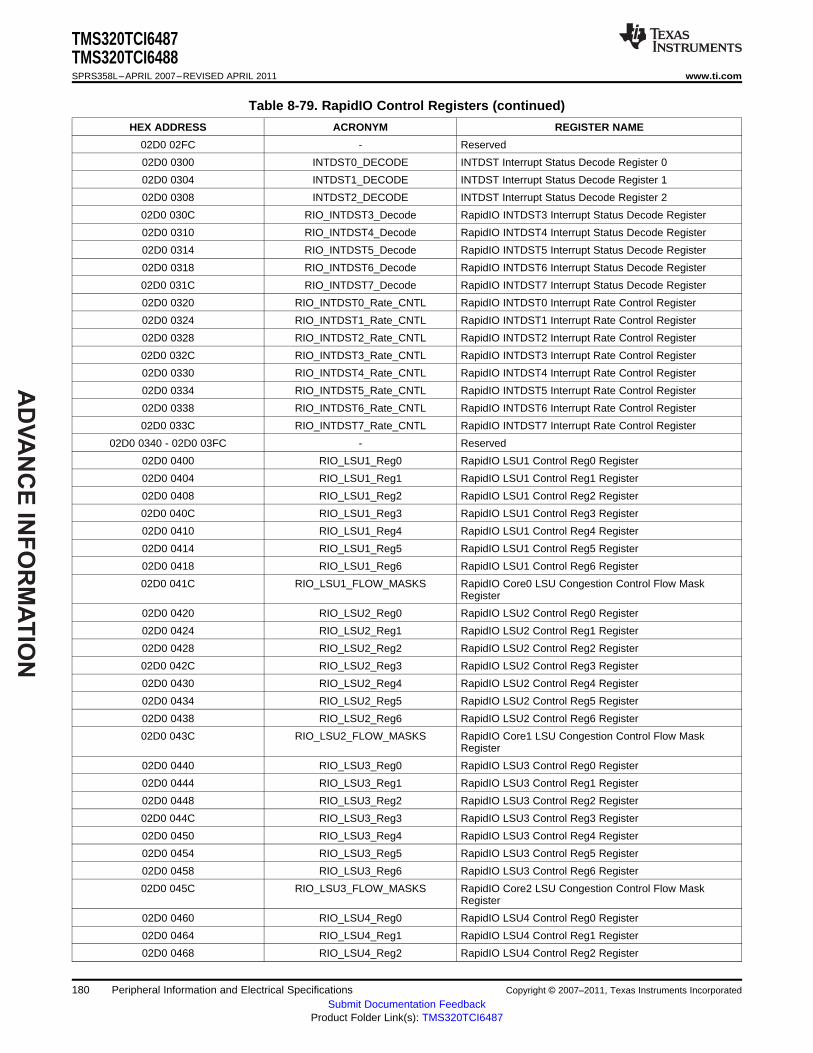
AD
VA
NC
E IN
FO
RM
AT
ION
TMS320TCI6487TMS320TCI6488SPRS358L–APRIL 2007–REVISED APRIL 2011 www.ti.com
Table 8-79. RapidIO Control Registers (continued)
HEX ADDRESS ACRONYM REGISTER NAME
02D0 02FC - Reserved
02D0 0300 INTDST0_DECODE INTDST Interrupt Status Decode Register 0
02D0 0304 INTDST1_DECODE INTDST Interrupt Status Decode Register 1
02D0 0308 INTDST2_DECODE INTDST Interrupt Status Decode Register 2
02D0 030C RIO_INTDST3_Decode RapidIO INTDST3 Interrupt Status Decode Register
02D0 0310 RIO_INTDST4_Decode RapidIO INTDST4 Interrupt Status Decode Register
02D0 0314 RIO_INTDST5_Decode RapidIO INTDST5 Interrupt Status Decode Register
02D0 0318 RIO_INTDST6_Decode RapidIO INTDST6 Interrupt Status Decode Register
02D0 031C RIO_INTDST7_Decode RapidIO INTDST7 Interrupt Status Decode Register
02D0 0320 RIO_INTDST0_Rate_CNTL RapidIO INTDST0 Interrupt Rate Control Register
02D0 0324 RIO_INTDST1_Rate_CNTL RapidIO INTDST1 Interrupt Rate Control Register
02D0 0328 RIO_INTDST2_Rate_CNTL RapidIO INTDST2 Interrupt Rate Control Register
02D0 032C RIO_INTDST3_Rate_CNTL RapidIO INTDST3 Interrupt Rate Control Register
02D0 0330 RIO_INTDST4_Rate_CNTL RapidIO INTDST4 Interrupt Rate Control Register
02D0 0334 RIO_INTDST5_Rate_CNTL RapidIO INTDST5 Interrupt Rate Control Register
02D0 0338 RIO_INTDST6_Rate_CNTL RapidIO INTDST6 Interrupt Rate Control Register
02D0 033C RIO_INTDST7_Rate_CNTL RapidIO INTDST7 Interrupt Rate Control Register
02D0 0340 - 02D0 03FC - Reserved
02D0 0400 RIO_LSU1_Reg0 RapidIO LSU1 Control Reg0 Register
02D0 0404 RIO_LSU1_Reg1 RapidIO LSU1 Control Reg1 Register
02D0 0408 RIO_LSU1_Reg2 RapidIO LSU1 Control Reg2 Register
02D0 040C RIO_LSU1_Reg3 RapidIO LSU1 Control Reg3 Register
02D0 0410 RIO_LSU1_Reg4 RapidIO LSU1 Control Reg4 Register
02D0 0414 RIO_LSU1_Reg5 RapidIO LSU1 Control Reg5 Register
02D0 0418 RIO_LSU1_Reg6 RapidIO LSU1 Control Reg6 Register
02D0 041C RIO_LSU1_FLOW_MASKS RapidIO Core0 LSU Congestion Control Flow MaskRegister
02D0 0420 RIO_LSU2_Reg0 RapidIO LSU2 Control Reg0 Register
02D0 0424 RIO_LSU2_Reg1 RapidIO LSU2 Control Reg1 Register
02D0 0428 RIO_LSU2_Reg2 RapidIO LSU2 Control Reg2 Register
02D0 042C RIO_LSU2_Reg3 RapidIO LSU2 Control Reg3 Register
02D0 0430 RIO_LSU2_Reg4 RapidIO LSU2 Control Reg4 Register
02D0 0434 RIO_LSU2_Reg5 RapidIO LSU2 Control Reg5 Register
02D0 0438 RIO_LSU2_Reg6 RapidIO LSU2 Control Reg6 Register
02D0 043C RIO_LSU2_FLOW_MASKS RapidIO Core1 LSU Congestion Control Flow MaskRegister
02D0 0440 RIO_LSU3_Reg0 RapidIO LSU3 Control Reg0 Register
02D0 0444 RIO_LSU3_Reg1 RapidIO LSU3 Control Reg1 Register
02D0 0448 RIO_LSU3_Reg2 RapidIO LSU3 Control Reg2 Register
02D0 044C RIO_LSU3_Reg3 RapidIO LSU3 Control Reg3 Register
02D0 0450 RIO_LSU3_Reg4 RapidIO LSU3 Control Reg4 Register
02D0 0454 RIO_LSU3_Reg5 RapidIO LSU3 Control Reg5 Register
02D0 0458 RIO_LSU3_Reg6 RapidIO LSU3 Control Reg6 Register
02D0 045C RIO_LSU3_FLOW_MASKS RapidIO Core2 LSU Congestion Control Flow MaskRegister
02D0 0460 RIO_LSU4_Reg0 RapidIO LSU4 Control Reg0 Register
02D0 0464 RIO_LSU4_Reg1 RapidIO LSU4 Control Reg1 Register
02D0 0468 RIO_LSU4_Reg2 RapidIO LSU4 Control Reg2 Register
180 Peripheral Information and Electrical Specifications Copyright © 2007–2011, Texas Instruments Incorporated
Submit Documentation FeedbackProduct Folder Link(s): TMS320TCI6487
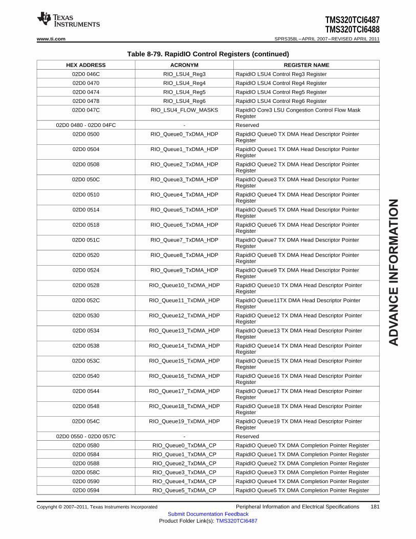
AD
VA
NC
E I
NF
OR
MA
TIO
N
TMS320TCI6487TMS320TCI6488
www.ti.com SPRS358L–APRIL 2007–REVISED APRIL 2011
Table 8-79. RapidIO Control Registers (continued)
HEX ADDRESS ACRONYM REGISTER NAME
02D0 046C RIO_LSU4_Reg3 RapidIO LSU4 Control Reg3 Register
02D0 0470 RIO_LSU4_Reg4 RapidIO LSU4 Control Reg4 Register
02D0 0474 RIO_LSU4_Reg5 RapidIO LSU4 Control Reg5 Register
02D0 0478 RIO_LSU4_Reg6 RapidIO LSU4 Control Reg6 Register
02D0 047C RIO_LSU4_FLOW_MASKS RapidIO Core3 LSU Congestion Control Flow MaskRegister
02D0 0480 - 02D0 04FC - Reserved
02D0 0500 RIO_Queue0_TxDMA_HDP RapidIO Queue0 TX DMA Head Descriptor PointerRegister
02D0 0504 RIO_Queue1_TxDMA_HDP RapidIO Queue1 TX DMA Head Descriptor PointerRegister
02D0 0508 RIO_Queue2_TxDMA_HDP RapidIO Queue2 TX DMA Head Descriptor PointerRegister
02D0 050C RIO_Queue3_TxDMA_HDP RapidIO Queue3 TX DMA Head Descriptor PointerRegister
02D0 0510 RIO_Queue4_TxDMA_HDP RapidIO Queue4 TX DMA Head Descriptor PointerRegister
02D0 0514 RIO_Queue5_TxDMA_HDP RapidIO Queue5 TX DMA Head Descriptor PointerRegister
02D0 0518 RIO_Queue6_TxDMA_HDP RapidIO Queue6 TX DMA Head Descriptor PointerRegister
02D0 051C RIO_Queue7_TxDMA_HDP RapidIO Queue7 TX DMA Head Descriptor PointerRegister
02D0 0520 RIO_Queue8_TxDMA_HDP RapidIO Queue8 TX DMA Head Descriptor PointerRegister
02D0 0524 RIO_Queue9_TxDMA_HDP RapidIO Queue9 TX DMA Head Descriptor PointerRegister
02D0 0528 RIO_Queue10_TxDMA_HDP RapidIO Queue10 TX DMA Head Descriptor PointerRegister
02D0 052C RIO_Queue11_TxDMA_HDP RapidIO Queue11TX DMA Head Descriptor PointerRegister
02D0 0530 RIO_Queue12_TxDMA_HDP RapidIO Queue12 TX DMA Head Descriptor PointerRegister
02D0 0534 RIO_Queue13_TxDMA_HDP RapidIO Queue13 TX DMA Head Descriptor PointerRegister
02D0 0538 RIO_Queue14_TxDMA_HDP RapidIO Queue14 TX DMA Head Descriptor PointerRegister
02D0 053C RIO_Queue15_TxDMA_HDP RapidIO Queue15 TX DMA Head Descriptor PointerRegister
02D0 0540 RIO_Queue16_TxDMA_HDP RapidIO Queue16 TX DMA Head Descriptor PointerRegister
02D0 0544 RIO_Queue17_TxDMA_HDP RapidIO Queue17 TX DMA Head Descriptor PointerRegister
02D0 0548 RIO_Queue18_TxDMA_HDP RapidIO Queue18 TX DMA Head Descriptor PointerRegister
02D0 054C RIO_Queue19_TxDMA_HDP RapidIO Queue19 TX DMA Head Descriptor PointerRegister
02D0 0550 - 02D0 057C - Reserved
02D0 0580 RIO_Queue0_TxDMA_CP RapidIO Queue0 TX DMA Completion Pointer Register
02D0 0584 RIO_Queue1_TxDMA_CP RapidIO Queue1 TX DMA Completion Pointer Register
02D0 0588 RIO_Queue2_TxDMA_CP RapidIO Queue2 TX DMA Completion Pointer Register
02D0 058C RIO_Queue3_TxDMA_CP RapidIO Queue3 TX DMA Completion Pointer Register
02D0 0590 RIO_Queue4_TxDMA_CP RapidIO Queue4 TX DMA Completion Pointer Register
02D0 0594 RIO_Queue5_TxDMA_CP RapidIO Queue5 TX DMA Completion Pointer Register
Copyright © 2007–2011, Texas Instruments Incorporated Peripheral Information and Electrical Specifications 181Submit Documentation Feedback
Product Folder Link(s): TMS320TCI6487

AD
VA
NC
E IN
FO
RM
AT
ION
TMS320TCI6487TMS320TCI6488SPRS358L–APRIL 2007–REVISED APRIL 2011 www.ti.com
Table 8-79. RapidIO Control Registers (continued)
HEX ADDRESS ACRONYM REGISTER NAME
02D0 0598 RIO_Queue6_TxDMA_CP RapidIO Queue6 TX DMA Completion Pointer Register
02D0 059C RIO_Queue7_TxDMA_CP RapidIO Queue7 TX DMA Completion Pointer Register
02D0 05A0 RIO_Queue8_TxDMA_CP RapidIO Queue8 TX DMA Completion Pointer Register
02D0 05A4 RIO_Queue9_TxDMA_CP RapidIO Queue9 TX DMA Completion Pointer Register
02D0 05A8 RIO_Queue10_TxDMA_CP RapidIO Queue10 TX DMA Completion Pointer Register
02D0 05AC RIO_Queue11_TxDMA_CP RapidIO Queue11 TX DMA Completion Pointer Register
02D0 05B0 RIO_Queue12_TxDMA_CP RapidIO Queue12 TX DMA Completion Pointer Register
02D0 05B4 RIO_Queue13_TxDMA_CP RapidIO Queue13 TX DMA Completion Pointer Register
02D0 05B8 RIO_Queue14_TxDMA_CP RapidIO Queue14 TX DMA Completion Pointer Register
02D0 05BC RIO_Queue15_TxDMA_CP RapidIO Queue15 TX DMA Completion Pointer Register
02D0 05C0 - 02D0 05FC - Reserved
02D0 0600 RIO_Queue0_RxDMA_HDP RapidIO Queue0 RX DMA Head Descriptor PointerRegister
02D0 0604 RIO_Queue1_RxDMA_HDP RapidIO Queue1 RX DMA Head Descriptor PointerRegister
02D0 0608 RIO_Queue2_RxDMA_HDP RapidIO Queue2 RX DMA Head Descriptor PointerRegister
02D0 060C RIO_Queue3_RxDMA_HDP RapidIO Queue3 RX DMA Head Descriptor PointerRegister
02D0 0610 RIO_Queue4_RxDMA_HDP RapidIO Queue4 RX DMA Head Descriptor PointerRegister
02D0 0614 RIO_Queue5_RxDMA_HDP RapidIO Queue5 RX DMA Head Descriptor PointerRegister
02D0 0618 RIO_Queue6_RxDMA_HDP RapidIO Queue6 RX DMA Head Descriptor PointerRegister
02D0 061C RIO_Queue7_RxDMA_HDP RapidIO Queue7 RX DMA Head Descriptor PointerRegister
02D0 0620 RIO_Queue8_RxDMA_HDP RapidIO Queue8 RX DMA Head Descriptor PointerRegister
02D0 0624 RIO_Queue9_RxDMA_HDP RapidIO Queue9 RX DMA Head Descriptor PointerRegister
02D0 0628 RIO_Queue10_RxDMA_HDP RapidIO Queue10 RX DMA Head Descriptor PointerRegister
02D0 062C RIO_Queue11_RxDMA_HDP RapidIO Queue11 RX DMA Head Descriptor PointerRegister
02D0 0630 RIO_Queue12_RxDMA_HDP RapidIO Queue12 RX DMA Head Descriptor PointerRegister
02D0 0634 RIO_Queue13_RxDMA_HDP RapidIO Queue13 RX DMA Head Descriptor PointerRegister
02D0 0638 RIO_Queue14_RxDMA_HDP RapidIO Queue14 RX DMA Head Descriptor PointerRegister
02D0 063C RIO_Queue15_RxDMA_HDP RapidIO Queue15 RX DMA Head Descriptor PointerRegister
02D0 0640 - 02D0 067C - Reserved
02D0 0680 RIO_Queue0_RxDMA_CP RapidIO Queue0 RX DMA Completion Pointer Register
02D0 0684 RIO_Queue1_RxDMA_CP RapidIO Queue1 RX DMA Completion Pointer Register
02D0 0688 RIO_Queue2_RxDMA_CP RapidIO Queue2 RX DMA Completion Pointer Register
02D0 068C RIO_Queue3_RxDMA_CP RapidIO Queue3 RX DMA Completion Pointer Register
02D0 0690 RIO_Queue4_RxDMA_CP RapidIO Queue4 RX DMA Completion Pointer Register
02D0 0694 RIO_Queue5_RxDMA_CP RapidIO Queue5 RX DMA Completion Pointer Register
02D0 0698 RIO_Queue6_RxDMA_CP RapidIO Queue6 RX DMA Completion Pointer Register
02D0 069C RIO_Queue7_RxDMA_CP RapidIO Queue7 RX DMA Completion Pointer Register
182 Peripheral Information and Electrical Specifications Copyright © 2007–2011, Texas Instruments Incorporated
Submit Documentation FeedbackProduct Folder Link(s): TMS320TCI6487
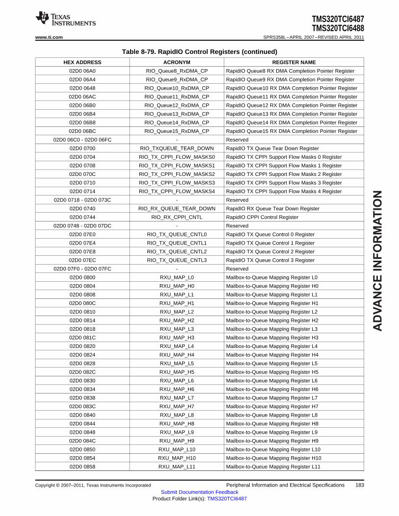
AD
VA
NC
E I
NF
OR
MA
TIO
N
TMS320TCI6487TMS320TCI6488
www.ti.com SPRS358L–APRIL 2007–REVISED APRIL 2011
Table 8-79. RapidIO Control Registers (continued)
HEX ADDRESS ACRONYM REGISTER NAME
02D0 06A0 RIO_Queue8_RxDMA_CP RapidIO Queue8 RX DMA Completion Pointer Register
02D0 06A4 RIO_Queue9_RxDMA_CP RapidIO Queue9 RX DMA Completion Pointer Register
02D0 0648 RIO_Queue10_RxDMA_CP RapidIO Queue10 RX DMA Completion Pointer Register
02D0 06AC RIO_Queue11_RxDMA_CP RapidIO Queue11 RX DMA Completion Pointer Register
02D0 06B0 RIO_Queue12_RxDMA_CP RapidIO Queue12 RX DMA Completion Pointer Register
02D0 06B4 RIO_Queue13_RxDMA_CP RapidIO Queue13 RX DMA Completion Pointer Register
02D0 06B8 RIO_Queue14_RxDMA_CP RapidIO Queue14 RX DMA Completion Pointer Register
02D0 06BC RIO_Queue15_RxDMA_CP RapidIO Queue15 RX DMA Completion Pointer Register
02D0 06C0 - 02D0 06FC - Reserved
02D0 0700 RIO_TXQUEUE_TEAR_DOWN RapidIO TX Queue Tear Down Register
02D0 0704 RIO_TX_CPPI_FLOW_MASKS0 RapidIO TX CPPI Support Flow Masks 0 Register
02D0 0708 RIO_TX_CPPI_FLOW_MASKS1 RapidIO TX CPPI Support Flow Masks 1 Register
02D0 070C RIO_TX_CPPI_FLOW_MASKS2 RapidIO TX CPPI Support Flow Masks 2 Register
02D0 0710 RIO_TX_CPPI_FLOW_MASKS3 RapidIO TX CPPI Support Flow Masks 3 Register
02D0 0714 RIO_TX_CPPI_FLOW_MASKS4 RapidIO TX CPPI Support Flow Masks 4 Register
02D0 0718 - 02D0 073C - Reserved
02D0 0740 RIO_RX_QUEUE_TEAR_DOWN RapidIO RX Queue Tear Down Register
02D0 0744 RIO_RX_CPPI_CNTL RapidIO CPPI Control Register
02D0 0748 - 02D0 07DC - Reserved
02D0 07E0 RIO_TX_QUEUE_CNTL0 RapidIO TX Queue Control 0 Register
02D0 07E4 RIO_TX_QUEUE_CNTL1 RapidIO TX Queue Control 1 Register
02D0 07E8 RIO_TX_QUEUE_CNTL2 RapidIO TX Queue Control 2 Register
02D0 07EC RIO_TX_QUEUE_CNTL3 RapidIO TX Queue Control 3 Register
02D0 07F0 - 02D0 07FC - Reserved
02D0 0800 RXU_MAP_L0 Mailbox-to-Queue Mapping Register L0
02D0 0804 RXU_MAP_H0 Mailbox-to-Queue Mapping Register H0
02D0 0808 RXU_MAP_L1 Mailbox-to-Queue Mapping Register L1
02D0 080C RXU_MAP_H1 Mailbox-to-Queue Mapping Register H1
02D0 0810 RXU_MAP_L2 Mailbox-to-Queue Mapping Register L2
02D0 0814 RXU_MAP_H2 Mailbox-to-Queue Mapping Register H2
02D0 0818 RXU_MAP_L3 Mailbox-to-Queue Mapping Register L3
02D0 081C RXU_MAP_H3 Mailbox-to-Queue Mapping Register H3
02D0 0820 RXU_MAP_L4 Mailbox-to-Queue Mapping Register L4
02D0 0824 RXU_MAP_H4 Mailbox-to-Queue Mapping Register H4
02D0 0828 RXU_MAP_L5 Mailbox-to-Queue Mapping Register L5
02D0 082C RXU_MAP_H5 Mailbox-to-Queue Mapping Register H5
02D0 0830 RXU_MAP_L6 Mailbox-to-Queue Mapping Register L6
02D0 0834 RXU_MAP_H6 Mailbox-to-Queue Mapping Register H6
02D0 0838 RXU_MAP_L7 Mailbox-to-Queue Mapping Register L7
02D0 083C RXU_MAP_H7 Mailbox-to-Queue Mapping Register H7
02D0 0840 RXU_MAP_L8 Mailbox-to-Queue Mapping Register L8
02D0 0844 RXU_MAP_H8 Mailbox-to-Queue Mapping Register H8
02D0 0848 RXU_MAP_L9 Mailbox-to-Queue Mapping Register L9
02D0 084C RXU_MAP_H9 Mailbox-to-Queue Mapping Register H9
02D0 0850 RXU_MAP_L10 Mailbox-to-Queue Mapping Register L10
02D0 0854 RXU_MAP_H10 Mailbox-to-Queue Mapping Register H10
02D0 0858 RXU_MAP_L11 Mailbox-to-Queue Mapping Register L11
Copyright © 2007–2011, Texas Instruments Incorporated Peripheral Information and Electrical Specifications 183Submit Documentation Feedback
Product Folder Link(s): TMS320TCI6487

AD
VA
NC
E IN
FO
RM
AT
ION
TMS320TCI6487TMS320TCI6488SPRS358L–APRIL 2007–REVISED APRIL 2011 www.ti.com
Table 8-79. RapidIO Control Registers (continued)
HEX ADDRESS ACRONYM REGISTER NAME
02D0 085C RXU_MAP_H11 Mailbox-to-Queue Mapping Register H11
02D0 08560 RXU_MAP_L12 Mailbox-to-Queue Mapping Register L12
02D0 0864 RXU_MAP_H12 Mailbox-to-Queue Mapping Register H12
02D0 0868 RXU_MAP_L13 Mailbox-to-Queue Mapping Register L13
02D0 086C RXU_MAP_H13 Mailbox-to-Queue Mapping Register H13
02D0 0870 RXU_MAP_L14 Mailbox-to-Queue Mapping Register L14
02D0 0874 RXU_MAP_H14 Mailbox-to-Queue Mapping Register H14
02D0 0878 RXU_MAP_L15 Mailbox-to-Queue Mapping Register L15
02D0 087C RXU_MAP_H15 Mailbox-to-Queue Mapping Register H15
02D0 0880 RXU_MAP_L16 Mailbox-to-Queue Mapping Register L16
02D0 0884 RXU_MAP_H16 Mailbox-to-Queue Mapping Register H16
02D0 0888 RXU_MAP_L17 Mailbox-to-Queue Mapping Register L17
02D0 088C RXU_MAP_H17 Mailbox-to-Queue Mapping Register H17
02D0 0890 RXU_MAP_L18 Mailbox-to-Queue Mapping Register L18
02D0 0894 RXU_MAP_H18 Mailbox-to-Queue Mapping Register H18
02D0 0898 RXU_MAP_L19 Mailbox-to-Queue Mapping Register L19
02D0 089C RXU_MAP_H19 Mailbox-to-Queue Mapping Register H19
02D0 08A0 RXU_MAP_L20 Mailbox-to-Queue Mapping Register L20
02D0 08A4 RXU_MAP_H20 Mailbox-to-Queue Mapping Register H20
02D0 08A8 RXU_MAP_L21 Mailbox-to-Queue Mapping Register L21
02D0 08AC RXU_MAP_H21 Mailbox-to-Queue Mapping Register H21
02D0 08B0 RXU_MAP_L22 Mailbox-to-Queue Mapping Register L22
02D0 08B4 RXU_MAP_H22 Mailbox-to-Queue Mapping Register H22
02D0 08B8 RXU_MAP_L23 Mailbox-to-Queue Mapping Register L23
02D0 08BC RXU_MAP_H23 Mailbox-to-Queue Mapping Register H23
02D0 08C0 RXU_MAP_L24 Mailbox-to-Queue Mapping Register L24
02D0 08C4 RXU_MAP_H24 Mailbox-to-Queue Mapping Register H24
02D0 08C8 RXU_MAP_L25 Mailbox-to-Queue Mapping Register L25
02D0 08CC RXU_MAP_H25 Mailbox-to-Queue Mapping Register H25
02D0 08D0 RXU_MAP_L26 Mailbox-to-Queue Mapping Register L26
02D0 08D4 RXU_MAP_H26 Mailbox-to-Queue Mapping Register H26
02D0 08D8 RXU_MAP_L27 Mailbox-to-Queue Mapping Register L27
02D0 08DC RXU_MAP_H27 Mailbox-to-Queue Mapping Register H27
02D0 08E0 RXU_MAP_L28 Mailbox-to-Queue Mapping Register L28
02D0 08E4 RXU_MAP_H28 Mailbox-to-Queue Mapping Register H28
02D0 08E8 RXU_MAP_L29 Mailbox-to-Queue Mapping Register L29
02D0 08EC RXU_MAP_H29 Mailbox-to-Queue Mapping Register H29
02D0 08F0 RXU_MAP_L30 Mailbox-to-Queue Mapping Register L30
02D0 08F4 RXU_MAP_H30 Mailbox-to-Queue Mapping Register H30
02D0 08F8 RXU_MAP_L31 Mailbox-to-Queue Mapping Register L31
02D0 08FC RXU_MAP_H31 Mailbox-to-Queue Mapping Register H31
02D0 0900 FLOW_CNTL0 Flow Control Table Entry Register 0
02D0 0904 FLOW_CNTL1 Flow Control Table Entry Register 1
02D0 0908 FLOW_CNTL2 Flow Control Table Entry Register 2
02D0 090C FLOW_CNTL3 Flow Control Table Entry Register 3
02D0 0910 FLOW_CNTL4 Flow Control Table Entry Register 4
02D0 0914 FLOW_CNTL5 Flow Control Table Entry Register 5
184 Peripheral Information and Electrical Specifications Copyright © 2007–2011, Texas Instruments Incorporated
Submit Documentation FeedbackProduct Folder Link(s): TMS320TCI6487
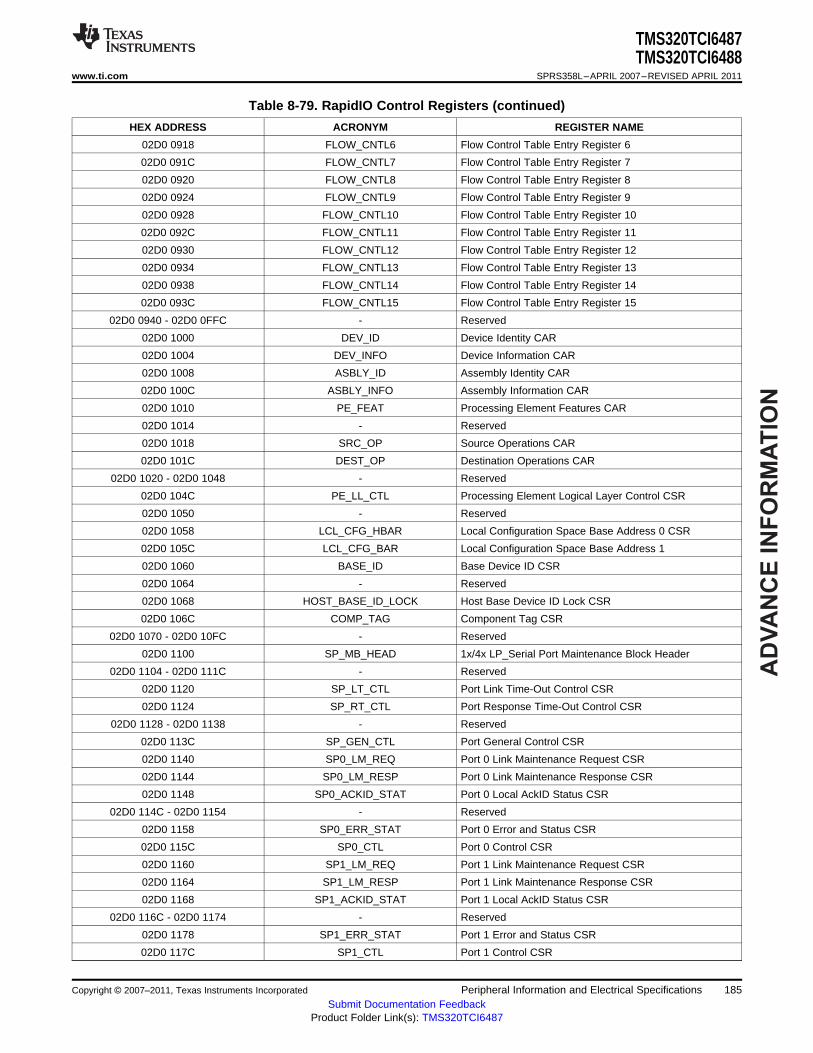
AD
VA
NC
E I
NF
OR
MA
TIO
N
TMS320TCI6487TMS320TCI6488
www.ti.com SPRS358L–APRIL 2007–REVISED APRIL 2011
Table 8-79. RapidIO Control Registers (continued)
HEX ADDRESS ACRONYM REGISTER NAME
02D0 0918 FLOW_CNTL6 Flow Control Table Entry Register 6
02D0 091C FLOW_CNTL7 Flow Control Table Entry Register 7
02D0 0920 FLOW_CNTL8 Flow Control Table Entry Register 8
02D0 0924 FLOW_CNTL9 Flow Control Table Entry Register 9
02D0 0928 FLOW_CNTL10 Flow Control Table Entry Register 10
02D0 092C FLOW_CNTL11 Flow Control Table Entry Register 11
02D0 0930 FLOW_CNTL12 Flow Control Table Entry Register 12
02D0 0934 FLOW_CNTL13 Flow Control Table Entry Register 13
02D0 0938 FLOW_CNTL14 Flow Control Table Entry Register 14
02D0 093C FLOW_CNTL15 Flow Control Table Entry Register 15
02D0 0940 - 02D0 0FFC - Reserved
02D0 1000 DEV_ID Device Identity CAR
02D0 1004 DEV_INFO Device Information CAR
02D0 1008 ASBLY_ID Assembly Identity CAR
02D0 100C ASBLY_INFO Assembly Information CAR
02D0 1010 PE_FEAT Processing Element Features CAR
02D0 1014 - Reserved
02D0 1018 SRC_OP Source Operations CAR
02D0 101C DEST_OP Destination Operations CAR
02D0 1020 - 02D0 1048 - Reserved
02D0 104C PE_LL_CTL Processing Element Logical Layer Control CSR
02D0 1050 - Reserved
02D0 1058 LCL_CFG_HBAR Local Configuration Space Base Address 0 CSR
02D0 105C LCL_CFG_BAR Local Configuration Space Base Address 1
02D0 1060 BASE_ID Base Device ID CSR
02D0 1064 - Reserved
02D0 1068 HOST_BASE_ID_LOCK Host Base Device ID Lock CSR
02D0 106C COMP_TAG Component Tag CSR
02D0 1070 - 02D0 10FC - Reserved
02D0 1100 SP_MB_HEAD 1x/4x LP_Serial Port Maintenance Block Header
02D0 1104 - 02D0 111C - Reserved
02D0 1120 SP_LT_CTL Port Link Time-Out Control CSR
02D0 1124 SP_RT_CTL Port Response Time-Out Control CSR
02D0 1128 - 02D0 1138 - Reserved
02D0 113C SP_GEN_CTL Port General Control CSR
02D0 1140 SP0_LM_REQ Port 0 Link Maintenance Request CSR
02D0 1144 SP0_LM_RESP Port 0 Link Maintenance Response CSR
02D0 1148 SP0_ACKID_STAT Port 0 Local AckID Status CSR
02D0 114C - 02D0 1154 - Reserved
02D0 1158 SP0_ERR_STAT Port 0 Error and Status CSR
02D0 115C SP0_CTL Port 0 Control CSR
02D0 1160 SP1_LM_REQ Port 1 Link Maintenance Request CSR
02D0 1164 SP1_LM_RESP Port 1 Link Maintenance Response CSR
02D0 1168 SP1_ACKID_STAT Port 1 Local AckID Status CSR
02D0 116C - 02D0 1174 - Reserved
02D0 1178 SP1_ERR_STAT Port 1 Error and Status CSR
02D0 117C SP1_CTL Port 1 Control CSR
Copyright © 2007–2011, Texas Instruments Incorporated Peripheral Information and Electrical Specifications 185Submit Documentation Feedback
Product Folder Link(s): TMS320TCI6487
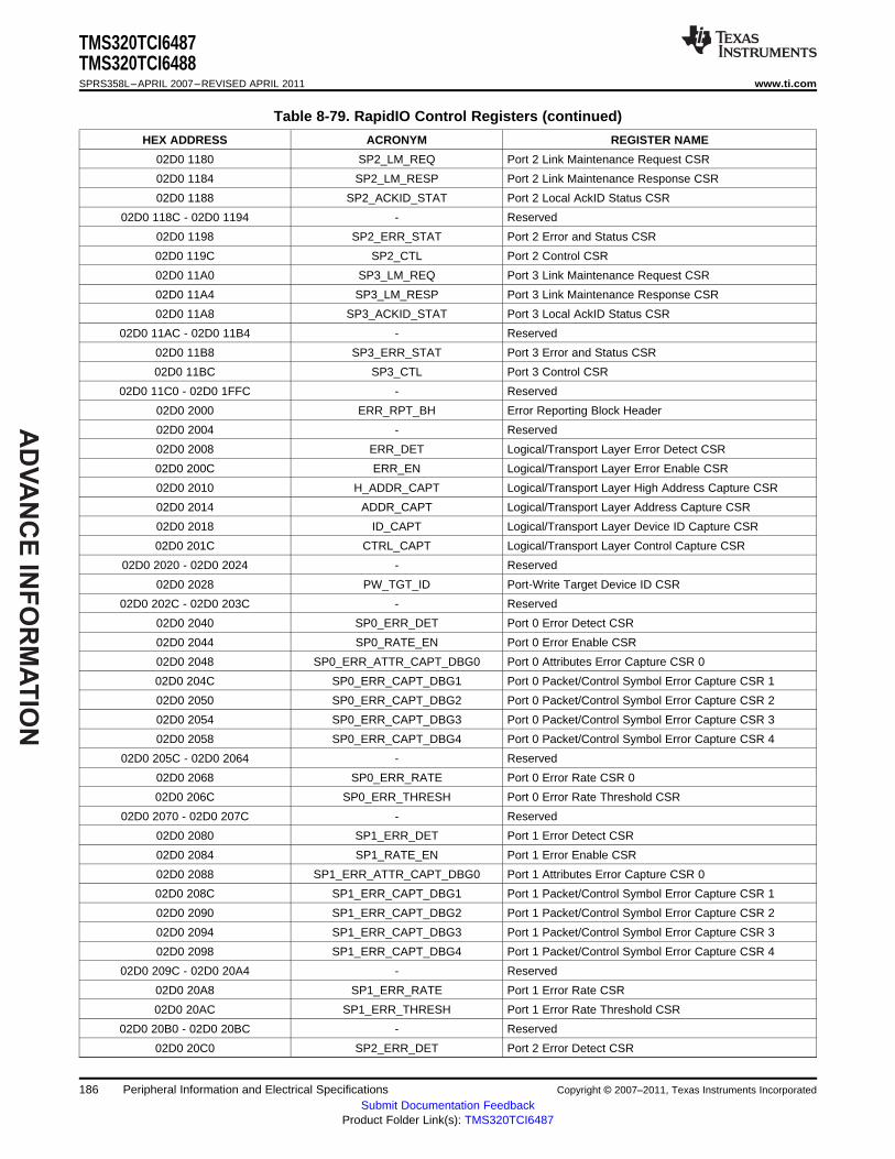
AD
VA
NC
E IN
FO
RM
AT
ION
TMS320TCI6487TMS320TCI6488SPRS358L–APRIL 2007–REVISED APRIL 2011 www.ti.com
Table 8-79. RapidIO Control Registers (continued)
HEX ADDRESS ACRONYM REGISTER NAME
02D0 1180 SP2_LM_REQ Port 2 Link Maintenance Request CSR
02D0 1184 SP2_LM_RESP Port 2 Link Maintenance Response CSR
02D0 1188 SP2_ACKID_STAT Port 2 Local AckID Status CSR
02D0 118C - 02D0 1194 - Reserved
02D0 1198 SP2_ERR_STAT Port 2 Error and Status CSR
02D0 119C SP2_CTL Port 2 Control CSR
02D0 11A0 SP3_LM_REQ Port 3 Link Maintenance Request CSR
02D0 11A4 SP3_LM_RESP Port 3 Link Maintenance Response CSR
02D0 11A8 SP3_ACKID_STAT Port 3 Local AckID Status CSR
02D0 11AC - 02D0 11B4 - Reserved
02D0 11B8 SP3_ERR_STAT Port 3 Error and Status CSR
02D0 11BC SP3_CTL Port 3 Control CSR
02D0 11C0 - 02D0 1FFC - Reserved
02D0 2000 ERR_RPT_BH Error Reporting Block Header
02D0 2004 - Reserved
02D0 2008 ERR_DET Logical/Transport Layer Error Detect CSR
02D0 200C ERR_EN Logical/Transport Layer Error Enable CSR
02D0 2010 H_ADDR_CAPT Logical/Transport Layer High Address Capture CSR
02D0 2014 ADDR_CAPT Logical/Transport Layer Address Capture CSR
02D0 2018 ID_CAPT Logical/Transport Layer Device ID Capture CSR
02D0 201C CTRL_CAPT Logical/Transport Layer Control Capture CSR
02D0 2020 - 02D0 2024 - Reserved
02D0 2028 PW_TGT_ID Port-Write Target Device ID CSR
02D0 202C - 02D0 203C - Reserved
02D0 2040 SP0_ERR_DET Port 0 Error Detect CSR
02D0 2044 SP0_RATE_EN Port 0 Error Enable CSR
02D0 2048 SP0_ERR_ATTR_CAPT_DBG0 Port 0 Attributes Error Capture CSR 0
02D0 204C SP0_ERR_CAPT_DBG1 Port 0 Packet/Control Symbol Error Capture CSR 1
02D0 2050 SP0_ERR_CAPT_DBG2 Port 0 Packet/Control Symbol Error Capture CSR 2
02D0 2054 SP0_ERR_CAPT_DBG3 Port 0 Packet/Control Symbol Error Capture CSR 3
02D0 2058 SP0_ERR_CAPT_DBG4 Port 0 Packet/Control Symbol Error Capture CSR 4
02D0 205C - 02D0 2064 - Reserved
02D0 2068 SP0_ERR_RATE Port 0 Error Rate CSR 0
02D0 206C SP0_ERR_THRESH Port 0 Error Rate Threshold CSR
02D0 2070 - 02D0 207C - Reserved
02D0 2080 SP1_ERR_DET Port 1 Error Detect CSR
02D0 2084 SP1_RATE_EN Port 1 Error Enable CSR
02D0 2088 SP1_ERR_ATTR_CAPT_DBG0 Port 1 Attributes Error Capture CSR 0
02D0 208C SP1_ERR_CAPT_DBG1 Port 1 Packet/Control Symbol Error Capture CSR 1
02D0 2090 SP1_ERR_CAPT_DBG2 Port 1 Packet/Control Symbol Error Capture CSR 2
02D0 2094 SP1_ERR_CAPT_DBG3 Port 1 Packet/Control Symbol Error Capture CSR 3
02D0 2098 SP1_ERR_CAPT_DBG4 Port 1 Packet/Control Symbol Error Capture CSR 4
02D0 209C - 02D0 20A4 - Reserved
02D0 20A8 SP1_ERR_RATE Port 1 Error Rate CSR
02D0 20AC SP1_ERR_THRESH Port 1 Error Rate Threshold CSR
02D0 20B0 - 02D0 20BC - Reserved
02D0 20C0 SP2_ERR_DET Port 2 Error Detect CSR
186 Peripheral Information and Electrical Specifications Copyright © 2007–2011, Texas Instruments Incorporated
Submit Documentation FeedbackProduct Folder Link(s): TMS320TCI6487
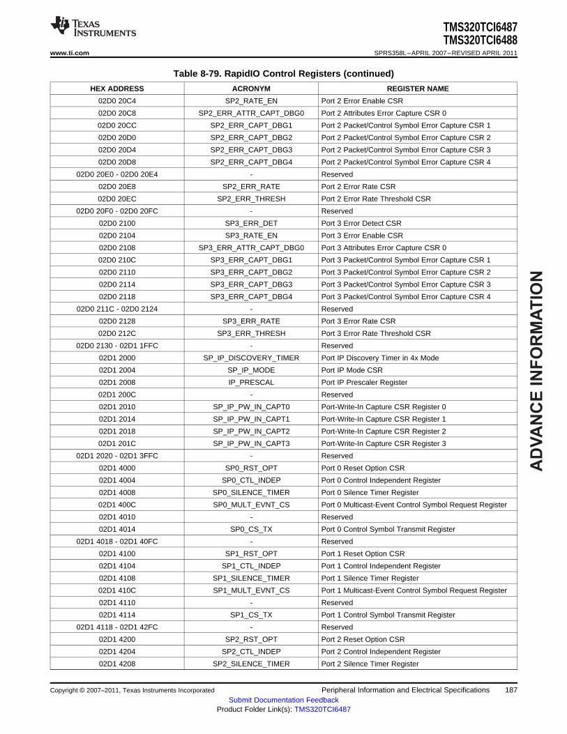
AD
VA
NC
E I
NF
OR
MA
TIO
N
TMS320TCI6487TMS320TCI6488
www.ti.com SPRS358L–APRIL 2007–REVISED APRIL 2011
Table 8-79. RapidIO Control Registers (continued)
HEX ADDRESS ACRONYM REGISTER NAME
02D0 20C4 SP2_RATE_EN Port 2 Error Enable CSR
02D0 20C8 SP2_ERR_ATTR_CAPT_DBG0 Port 2 Attributes Error Capture CSR 0
02D0 20CC SP2_ERR_CAPT_DBG1 Port 2 Packet/Control Symbol Error Capture CSR 1
02D0 20D0 SP2_ERR_CAPT_DBG2 Port 2 Packet/Control Symbol Error Capture CSR 2
02D0 20D4 SP2_ERR_CAPT_DBG3 Port 2 Packet/Control Symbol Error Capture CSR 3
02D0 20D8 SP2_ERR_CAPT_DBG4 Port 2 Packet/Control Symbol Error Capture CSR 4
02D0 20E0 - 02D0 20E4 - Reserved
02D0 20E8 SP2_ERR_RATE Port 2 Error Rate CSR
02D0 20EC SP2_ERR_THRESH Port 2 Error Rate Threshold CSR
02D0 20F0 - 02D0 20FC - Reserved
02D0 2100 SP3_ERR_DET Port 3 Error Detect CSR
02D0 2104 SP3_RATE_EN Port 3 Error Enable CSR
02D0 2108 SP3_ERR_ATTR_CAPT_DBG0 Port 3 Attributes Error Capture CSR 0
02D0 210C SP3_ERR_CAPT_DBG1 Port 3 Packet/Control Symbol Error Capture CSR 1
02D0 2110 SP3_ERR_CAPT_DBG2 Port 3 Packet/Control Symbol Error Capture CSR 2
02D0 2114 SP3_ERR_CAPT_DBG3 Port 3 Packet/Control Symbol Error Capture CSR 3
02D0 2118 SP3_ERR_CAPT_DBG4 Port 3 Packet/Control Symbol Error Capture CSR 4
02D0 211C - 02D0 2124 - Reserved
02D0 2128 SP3_ERR_RATE Port 3 Error Rate CSR
02D0 212C SP3_ERR_THRESH Port 3 Error Rate Threshold CSR
02D0 2130 - 02D1 1FFC - Reserved
02D1 2000 SP_IP_DISCOVERY_TIMER Port IP Discovery Timer in 4x Mode
02D1 2004 SP_IP_MODE Port IP Mode CSR
02D1 2008 IP_PRESCAL Port IP Prescaler Register
02D1 200C - Reserved
02D1 2010 SP_IP_PW_IN_CAPT0 Port-Write-In Capture CSR Register 0
02D1 2014 SP_IP_PW_IN_CAPT1 Port-Write-In Capture CSR Register 1
02D1 2018 SP_IP_PW_IN_CAPT2 Port-Write-In Capture CSR Register 2
02D1 201C SP_IP_PW_IN_CAPT3 Port-Write-In Capture CSR Register 3
02D1 2020 - 02D1 3FFC - Reserved
02D1 4000 SP0_RST_OPT Port 0 Reset Option CSR
02D1 4004 SP0_CTL_INDEP Port 0 Control Independent Register
02D1 4008 SP0_SILENCE_TIMER Port 0 Silence Timer Register
02D1 400C SP0_MULT_EVNT_CS Port 0 Multicast-Event Control Symbol Request Register
02D1 4010 - Reserved
02D1 4014 SP0_CS_TX Port 0 Control Symbol Transmit Register
02D1 4018 - 02D1 40FC - Reserved
02D1 4100 SP1_RST_OPT Port 1 Reset Option CSR
02D1 4104 SP1_CTL_INDEP Port 1 Control Independent Register
02D1 4108 SP1_SILENCE_TIMER Port 1 Silence Timer Register
02D1 410C SP1_MULT_EVNT_CS Port 1 Multicast-Event Control Symbol Request Register
02D1 4110 - Reserved
02D1 4114 SP1_CS_TX Port 1 Control Symbol Transmit Register
02D1 4118 - 02D1 42FC - Reserved
02D1 4200 SP2_RST_OPT Port 2 Reset Option CSR
02D1 4204 SP2_CTL_INDEP Port 2 Control Independent Register
02D1 4208 SP2_SILENCE_TIMER Port 2 Silence Timer Register
Copyright © 2007–2011, Texas Instruments Incorporated Peripheral Information and Electrical Specifications 187Submit Documentation Feedback
Product Folder Link(s): TMS320TCI6487

AD
VA
NC
E IN
FO
RM
AT
ION
2
1
3
4
4
SRIOSGMIIREFCLK(N|P)
TMS320TCI6487TMS320TCI6488SPRS358L–APRIL 2007–REVISED APRIL 2011 www.ti.com
Table 8-79. RapidIO Control Registers (continued)
HEX ADDRESS ACRONYM REGISTER NAME
02D1 420C SP2_MULT_EVNT_CS Port 2 Multicast-Event Control Symbol Request Register
02D1 4210 - Reserved
02D1 4214 SP2_CS_TX Port 2 Control Symbol Transmit Register
02D1 4218 - 02D1 42FC - Reserved
02D1 4300 SP3_RST_OPT Port 3 Reset Option CSR
02D1 4304 SP3_CTL_INDEP Port 3 Control Independent Register
02D1 4308 SP3_SILENCE_TIMER Port 3 Silence Timer Register
02D1 430C SP3_MULT_EVNT_CS Port 3 Multicast-Event Control Symbol Request Register
02D1 4310 - Reserved
02D1 4314 SP3_CS_TX Port 3 Control Symbol Transmit Register
02D1 4318 - 02D2 0FFF - Reserved
02D2 1000 - 02DF FFFF - Reserved
8.18.3 Serial RapidIO Electrical Data/Timing
Serial RapidIO is electrically compliant with the RapidIO™ Interconnect Specification, Part VI: PhysicalLayer 1x/4x LP-Serial Specification, Revision 1.2.
Table 8-80. Timing Requirements for SRIOSGMIIREFCLK(N|P) (1)
(see Figure 8-43)
NO. PARAMETERS MIN MAX UNIT
1 tc(SRIOSGMIIREFCLK) Cycle time, SRIOSGMIIREFCLK(N|P) 3.2 8 ns
2 tw(CLKH) Pulse duration, CLK(N|P) high 0.4C ns
3 tw(CLKL) Pulse duration, CLK(N|P) low 0.4C ns
4 tt(CLK) Transition time, CLK(N|P) 50 1300 ps
5 tj(CLK) Period Jitter (RMS), CLK(N|P) 4 ps
(1) C=1/SRIOSGMIIREFCLK(N|P)
Figure 8-43. SRIOSGMIIREFCLK(N|P) Timing
188 Peripheral Information and Electrical Specifications Copyright © 2007–2011, Texas Instruments Incorporated
Submit Documentation FeedbackProduct Folder Link(s): TMS320TCI6487
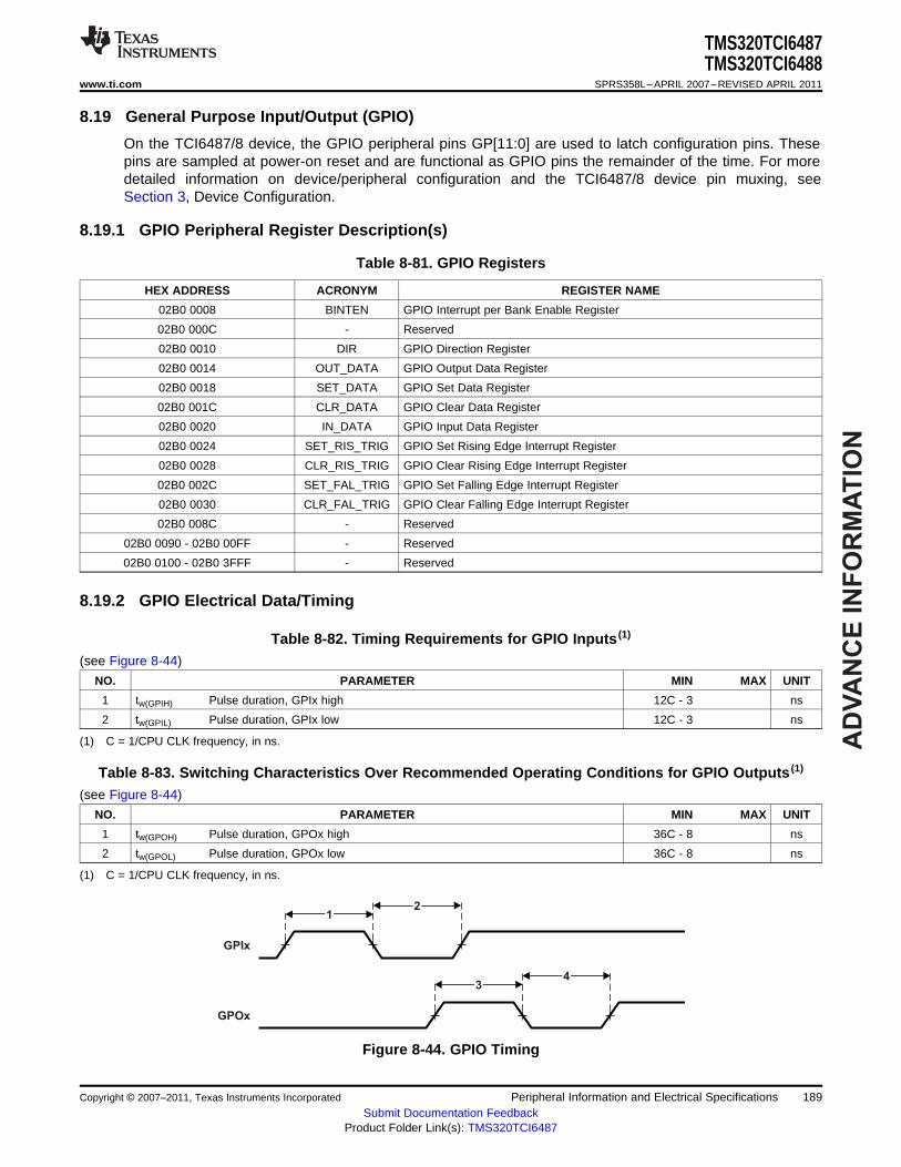
AD
VA
NC
E I
NF
OR
MA
TIO
N
12
34
GPIx
GPOx
TMS320TCI6487TMS320TCI6488
www.ti.com SPRS358L–APRIL 2007–REVISED APRIL 2011
8.19 General Purpose Input/Output (GPIO)
On the TCI6487/8 device, the GPIO peripheral pins GP[11:0] are used to latch configuration pins. Thesepins are sampled at power-on reset and are functional as GPIO pins the remainder of the time. For moredetailed information on device/peripheral configuration and the TCI6487/8 device pin muxing, seeSection 3, Device Configuration.
8.19.1 GPIO Peripheral Register Description(s)
Table 8-81. GPIO Registers
HEX ADDRESS ACRONYM REGISTER NAME
02B0 0008 BINTEN GPIO Interrupt per Bank Enable Register
02B0 000C - Reserved
02B0 0010 DIR GPIO Direction Register
02B0 0014 OUT_DATA GPIO Output Data Register
02B0 0018 SET_DATA GPIO Set Data Register
02B0 001C CLR_DATA GPIO Clear Data Register
02B0 0020 IN_DATA GPIO Input Data Register
02B0 0024 SET_RIS_TRIG GPIO Set Rising Edge Interrupt Register
02B0 0028 CLR_RIS_TRIG GPIO Clear Rising Edge Interrupt Register
02B0 002C SET_FAL_TRIG GPIO Set Falling Edge Interrupt Register
02B0 0030 CLR_FAL_TRIG GPIO Clear Falling Edge Interrupt Register
02B0 008C - Reserved
02B0 0090 - 02B0 00FF - Reserved
02B0 0100 - 02B0 3FFF - Reserved
8.19.2 GPIO Electrical Data/Timing
Table 8-82. Timing Requirements for GPIO Inputs (1)
(see Figure 8-44)
NO. PARAMETER MIN MAX UNIT
1 tw(GPIH) Pulse duration, GPIx high 12C - 3 ns
2 tw(GPIL) Pulse duration, GPIx low 12C - 3 ns
(1) C = 1/CPU CLK frequency, in ns.
Table 8-83. Switching Characteristics Over Recommended Operating Conditions for GPIO Outputs (1)
(see Figure 8-44)
NO. PARAMETER MIN MAX UNIT
1 tw(GPOH) Pulse duration, GPOx high 36C - 8 ns
2 tw(GPOL) Pulse duration, GPOx low 36C - 8 ns
(1) C = 1/CPU CLK frequency, in ns.
Figure 8-44. GPIO Timing
Copyright © 2007–2011, Texas Instruments Incorporated Peripheral Information and Electrical Specifications 189Submit Documentation Feedback
Product Folder Link(s): TMS320TCI6487
AD
VA
NC
E IN
FO
RM
AT
ION
TMS320TCI6487TMS320TCI6488SPRS358L–APRIL 2007–REVISED APRIL 2011 www.ti.com
8.20 Emulation Features and Capability
8.20.1 Advanced Event Triggering (AET)
The TCI6487/8 device supports Advanced Event Triggering (AET). This capability can be used to debugcomplex problems as well as understand performance characteristics of user applications. AET providesthe following capabilities:• Hardware Program Breakpoints: specify addresses or address ranges that can generate events such
as halting the processor or triggering the trace capture.• Data Watchpoints: specify data variable addresses, address ranges, or data values that can generate
events such as halting the processor or triggering the trace capture.• Counters: count the occurrence of an event or cycles for performance monitoring.• State Sequencing: allows combinations of hardware program breakpoints and data watchpoints to
precisely generate events for complex sequences.
For more information on AET, see the following documents:
Using Advanced Event Triggering to Find and Fix Intermittent Real-Time Bugs application report (literaturenumber SPRA753)
Using Advanced Event Triggering to Debug Real-Time Problems in High Speed EmbeddedMicroprocessor Systems application report (literature number SPRA387)
190 Peripheral Information and Electrical Specifications Copyright © 2007–2011, Texas Instruments Incorporated
Submit Documentation FeedbackProduct Folder Link(s): TMS320TCI6487
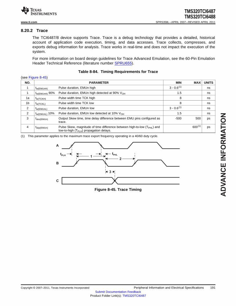
AD
VA
NC
E I
NF
OR
MA
TIO
N
A
B
C
tPLH
tPHL
12
3
TMS320TCI6487TMS320TCI6488
www.ti.com SPRS358L–APRIL 2007–REVISED APRIL 2011
8.20.2 Trace
The TCI6487/8 device supports Trace. Trace is a debug technology that provides a detailed, historicalaccount of application code execution, timing, and data accesses. Trace collects, compresses, andexports debug information for analysis. Trace works in real-time and does not impact the execution of thesystem.
For more information on board design guidelines for Trace Advanced Emulation, see the 60-Pin EmulationHeader Technical Reference (literature number SPRU655).
Table 8-84. Timing Requirements for Trace(see Figure 8-45)
NO. PARAMETER MIN MAX UNITS
1 tw(EMUnH) Pulse duration, EMUn high 3 - 0.6 (1) ns
1 tw(EMUnH) 90% Pulse duration, EMUn high detected at 90% VOH 1.5 ns
1a tw(TCKH) Pulse width time TCK high 8 ns
1b tw(TCKL) Pulse width time TCK low 8 ns
2 tw(EMUnL) Pulse duration, EMUn low 3 - 0.6 (1) ns
2 tw(EMUnL) 10% Pulse duration, EMUn low detected at 10% VOH 1.5 ns
3 tsko(EMUn) Output Skew time, time delay difference between EMU pins configured as -500 500 pstrace.
4 tskp(EMUn) Pulse Skew, magnitude of time difference between high-to-low (TPHL) and 600 (1) pslow-to-high (TPLH) propagation delays.
(1) This parameter applies to the maximum trace export frequency operating in a 40/60 duty cycle.
Figure 8-45. Trace Timing
Copyright © 2007–2011, Texas Instruments Incorporated Peripheral Information and Electrical Specifications 191Submit Documentation Feedback
Product Folder Link(s): TMS320TCI6487

AD
VA
NC
E IN
FO
RM
AT
ION
1
2
34
TCK
TDO
TDI/TMS
1a 1b
TMS320TCI6487TMS320TCI6488SPRS358L–APRIL 2007–REVISED APRIL 2011 www.ti.com
8.20.3 IEEE 1149.1 JTAG
The JTAG interface is used to support boundary scan and emulation of the device. The boundary scansupported allows for an asynchronous TRST and only the 5 baseline JTAG signals (e.g. no EMU[1:0])required for boundary scan. Most interfaces on the device follow the Boundary Scan Test Specification(IEEE1149.1), while all of the SerDes (Antenna Interface, RapidIO, and SGMII) support the AC couplednet test defined in AC Coupled Net Test Specification (IEEE1149.6).
It is expected that all compliant devices are connected through the same JTAG interface, in daisy-chainfashion, as per the specification. The JTAG interface uses 1.8-V buffers, compliant with the Power SupplyVoltage and Interface Standard for Nonterminated Digital Integrated Circuit Specification (EAI/JESD8-5).
8.20.3.1 IEEE 1149.1 JTAG Compatibility Statement
For maximum reliability, the TCI6487/8 DSP includes an internal pulldown (IPD) on the TRST pin toensure that TRST will always be asserted upon power up and the DSP's internal emulation logic willalways be properly initialized when this pin is not routed out. JTAG controllers from Texas Instrumentsactively drive TRST high. However, some third-party JTAG controllers may not drive TRST high but expectthe use of an external pullup resistor on TRST. When using this type of JTAG controller, assert TRST toinitialize the DSP after powerup and externally drive TRST high before attempting any emulation orboundary scan operations.
8.20.3.2 JTAG Electrical Data/Timing
Table 8-85. Timing Requirements for JTAG(see Figure 8-46)
NO. PARAMETER MIN MAX UNITS
1 tc(TCK) Cycle time, TCK 20 ns
1a tw(TCKH) Pulse width time TCK high 8 ns
1b tw(TCKL) Pulse width time TCK low 8 ns
2 td(TCKL-TDOV) Delay time, TCK low to TDO valid 0 8 ns
3a tsu(TDIV-TCKH) Setup time, TDI valid before TCK high 2 ns
3b tsu(TMSV-TCKH) Setup time, TMS valid before TCK high 2 ns
4a th(TCKH-TDIV) Hold time, TDI valid after TCK high 10 ns
4b th(TCKH-TMSV) Hold time, TMS valid after TCK high 10 ns
Figure 8-46. JTAG Timing
192 Peripheral Information and Electrical Specifications Copyright © 2007–2011, Texas Instruments Incorporated
Submit Documentation FeedbackProduct Folder Link(s): TMS320TCI6487
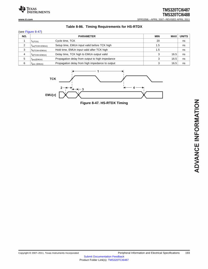
AD
VA
NC
E I
NF
OR
MA
TIO
N
1
342
TCK
EMU[ ]n
TMS320TCI6487TMS320TCI6488
www.ti.com SPRS358L–APRIL 2007–REVISED APRIL 2011
Table 8-86. Timing Requirements for HS-RTDX(see Figure 8-47)
NO. PARAMETER MIN MAX UNITS
1 tc(TCK) Cycle time, TCK 20 ns
2 tsu(TCKH-EMUn) Setup time, EMUn input valid before TCK high 1.5 ns
3 th(TCKH-EMUn) Hold time, EMUn input valid after TCK high 1.5 ns
4 td(TCKH-EMUn) Delay time, TCK high to EMUn output valid 3 16.5 ns
5 tpoz(EMUn) Propagation delay from output to high impedance 3 16.5 ns
6 tpzo (EMUn) Propagation delay from high impedance to output 3 16.5 ns
Figure 8-47. HS-RTDX Timing
Copyright © 2007–2011, Texas Instruments Incorporated Peripheral Information and Electrical Specifications 193Submit Documentation Feedback
Product Folder Link(s): TMS320TCI6487
AD
VA
NC
E IN
FO
RM
AT
ION
TMS320TCI6487TMS320TCI6488SPRS358L–APRIL 2007–REVISED APRIL 2011 www.ti.com
8.21 Semaphore
The device contains the Semaphore module for the management of shared resources of the DSP cores.The Semaphore enforces atomic accesses to shared chip-level resources so that the read-modify-writesequence is not broken. The semaphore block has unique interrupts to each of the cores to identify whenthat core has acquired the resource.
Semaphore resources within the module are not tied to specific hardware resources. It is a softwarerequirement to allocate semaphore resources to the hardware resource(s) to be arbitrated.
The Semaphore module supports 3 masters and contains 32 semaphores to be used within the system.There are two methods of accessing a semaphore resource:• Direct Access: A core directly accesses a semaphore resource. If free, the semaphore will be granted.
If not, the semaphore is not granted.• Indirect Access: A core indirectly accesses a semaphore resource by writing it. Once it is free, an
interrupt notifies the CPU that it is available.
8.21.1 Semaphore Register Description(s)
Table 8-87. Semaphore Registers
HEX ADDRESS ACRONYM REGISTER NAME
02B4 0000 SEM_PID Semaphore Peripheral Revision ID Register
02B4 000C SEM_EOI Semaphore EOI Register
02B4 0100 SEM_DIRECT0 Semaphore Direct0 Register
02B4 0104 SEM_DIRECT1 Semaphore Direct1 Register
02B4 0108 SEM_DIRECT2 Semaphore Direct2 Register
02B4 010C SEM_DIRECT3 Semaphore Direct3 Register
02B4 0110 SEM_DIRECT4 Semaphore Direct4 Register
02B4 0114 SEM_DIRECT5 Semaphore Direct5 Register
02B4 0118 SEM_DIRECT6 Semaphore Direct6 Register
02B4 011C SEM_DIRECT7 Semaphore Direct7 Register
02B4 0120 SEM_DIRECT8 Semaphore Direct8 Register
02B4 0124 SEM_DIRECT9 Semaphore Direct9 Register
02B4 0128 SEM_DIRECT10 Semaphore Direct10 Register
02B4 012C SEM_DIRECT11 Semaphore Direct11 Register
02B4 0130 SEM_DIRECT12 Semaphore Direct12 Register
02B4 0134 SEM_DIRECT13 Semaphore Direct13 Register
02B4 0138 SEM_DIRECT14 Semaphore Direct14 Register
02B4 013C SEM_DIRECT15 Semaphore Direct15 Register
02B4 0140 SEM_DIRECT16 Semaphore Direct16 Register
02B4 0144 SEM_DIRECT17 Semaphore Direct17 Register
02B4 0148 SEM_DIRECT18 Semaphore Direct18 Register
02B4 014C SEM_DIRECT19 Semaphore Direct19 Register
02B4 0150 SEM_DIRECT20 Semaphore Direct20 Register
02B4 0154 SEM_DIRECT21 Semaphore Direct21 Register
02B4 0158 SEM_DIRECT22 Semaphore Direct22 Register
02B4 015C SEM_DIRECT23 Semaphore Direct23 Register
02B4 0160 SEM_DIRECT24 Semaphore Direct24 Register
02B4 0164 SEM_DIRECT25 Semaphore Direct25 Register
02B4 0168 SEM_DIRECT26 Semaphore Direct26 Register
02B4 016C SEM_DIRECT27 Semaphore Direct27 Register
02B4 0170 SEM_DIRECT28 Semaphore Direct28 Register
194 Peripheral Information and Electrical Specifications Copyright © 2007–2011, Texas Instruments Incorporated
Submit Documentation FeedbackProduct Folder Link(s): TMS320TCI6487
AD
VA
NC
E I
NF
OR
MA
TIO
N
TMS320TCI6487TMS320TCI6488
www.ti.com SPRS358L–APRIL 2007–REVISED APRIL 2011
Table 8-87. Semaphore Registers (continued)
HEX ADDRESS ACRONYM REGISTER NAME
02B4 0174 SEM_DIRECT29 Semaphore Direct29 Register
02B4 0178 SEM_DIRECT30 Semaphore Direct30 Register
02B4 017C SEM_DIRECT31 Semaphore Direct31 Register
02B4 0200 SEM_INDIRECT0 Semaphore Indirect0 Register
02B4 0204 SEM_INDIRECT1 Semaphore Indirect1 Register
02B4 0208 SEM_INDIRECT2 Semaphore Indirect2 Register
02B4 020C SEM_INDIRECT3 Semaphore Indirect3 Register
02B4 0210 SEM_INDIRECT4 Semaphore Indirect4 Register
02B4 0214 SEM_INDIRECT5 Semaphore Indirect5 Register
02B4 0218 SEM_INDIRECT6 Semaphore Indirect6 Register
02B4 021C SEM_INDIRECT7 Semaphore Indirect7 Register
02B4 0220 SEM_INDIRECT8 Semaphore Indirect8 Register
02B4 0224 SEM_INDIRECT9 Semaphore Indirect9 Register
02B4 0228 SEM_INDIRECT10 Semaphore Indirect10 Register
02B4 022C SEM_INDIRECT11 Semaphore Indirect11 Register
02B4 0230 SEM_INDIRECT12 Semaphore Indirect12 Register
02B4 0234 SEM_INDIRECT13 Semaphore Indirect13 Register
02B4 0238 SEM_INDIRECT14 Semaphore Indirect14 Register
02B4 023C SEM_INDIRECT15 Semaphore Indirect15 Register
02B4 0240 SEM_INDIRECT16 Semaphore Indirect16 Register
02B4 0244 SEM_INDIRECT17 Semaphore Indirect17 Register
02B4 0248 SEM_INDIRECT18 Semaphore Indirect18 Register
02B4 024C SEM_INDIRECT19 Semaphore Indirect19 Register
02B4 0250 SEM_INDIRECT20 Semaphore Indirect20 Register
02B4 0254 SEM_INDIRECT21 Semaphore Indirect21 Register
02B4 0258 SEM_INDIRECT22 Semaphore Indirect22 Register
02B4 025C SEM_INDIRECT23 Semaphore Indirect23 Register
02B4 0260 SEM_INDIRECT24 Semaphore Indirect24 Register
02B4 0264 SEM_INDIRECT25 Semaphore Indirect25 Register
02B4 0268 SEM_INDIRECT26 Semaphore Indirect26 Register
02B4 026C SEM_INDIRECT27 Semaphore Indirect27 Register
02B4 0270 SEM_INDIRECT28 Semaphore Indirect28 Register
02B4 0274 SEM_INDIRECT29 Semaphore Indirect29 Register
02B4 0278 SEM_INDIRECT30 Semaphore Indirect30 Register
02B4 027C SEM_INDIRECT31 Semaphore Indirect31 Register
02B4 0300 SEM_QUERY0 Semaphore Query0 Register
02B4 0304 SEM_QUERY1 Semaphore Query1 Register
02B4 0308 SEM_QUERY2 Semaphore Query2 Register
02B4 030C SEM_QUERY3 Semaphore Query3 Register
02B4 0310 SEM_QUERY4 Semaphore Query4 Register
02B4 0314 SEM_QUERY5 Semaphore Query5 Register
02B4 0318 SEM_QUERY6 Semaphore Query6 Register
02B4 031C SEM_QUERY7 Semaphore Query7 Register
02B4 0320 SEM_QUERY8 Semaphore Query8 Register
02B4 0324 SEM_QUERY9 Semaphore Query9 Register
02B4 0328 SEM_QUERY10 Semaphore Query10 Register
02B4 032C SEM_QUERY11 Semaphore Query11 Register
Copyright © 2007–2011, Texas Instruments Incorporated Peripheral Information and Electrical Specifications 195Submit Documentation Feedback
Product Folder Link(s): TMS320TCI6487
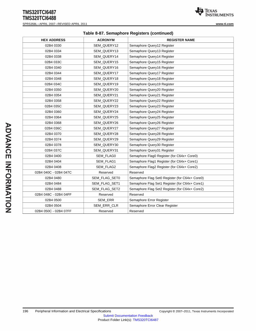
AD
VA
NC
E IN
FO
RM
AT
ION
TMS320TCI6487TMS320TCI6488SPRS358L–APRIL 2007–REVISED APRIL 2011 www.ti.com
Table 8-87. Semaphore Registers (continued)
HEX ADDRESS ACRONYM REGISTER NAME
02B4 0330 SEM_QUERY12 Semaphore Query12 Register
02B4 0334 SEM_QUERY13 Semaphore Query13 Register
02B4 0338 SEM_QUERY14 Semaphore Query14 Register
02B4 033C SEM_QUERY15 Semaphore Query15 Register
02B4 0340 SEM_QUERY16 Semaphore Query16 Register
02B4 0344 SEM_QUERY17 Semaphore Query17 Register
02B4 0348 SEM_QUERY18 Semaphore Query18 Register
02B4 034C SEM_QUERY19 Semaphore Query19 Register
02B4 0350 SEM_QUERY20 Semaphore Query20 Register
02B4 0354 SEM_QUERY21 Semaphore Query21 Register
02B4 0358 SEM_QUERY22 Semaphore Query22 Register
02B4 035C SEM_QUERY23 Semaphore Query23 Register
02B4 0360 SEM_QUERY24 Semaphore Query24 Register
02B4 0364 SEM_QUERY25 Semaphore Query25 Register
02B4 0368 SEM_QUERY26 Semaphore Query26 Register
02B4 036C SEM_QUERY27 Semaphore Query27 Register
02B4 0370 SEM_QUERY28 Semaphore Query28 Register
02B4 0374 SEM_QUERY29 Semaphore Query29 Register
02B4 0378 SEM_QUERY30 Semaphore Query30 Register
02B4 037C SEM_QUERY31 Semaphore Query31 Register
02B4 0400 SEM_FLAG0 Semaphore Flag0 Register (for C64x+ Core0)
02B4 0404 SEM_FLAG1 Semaphore Flag1 Register (for C64x+ Core1)
02B4 0408 SEM_FLAG2 Semaphore Flag2 Register (for C64x+ Core2)
02B4 040C - 02B4 047C Reserved Reserved
02B4 0480 SEM_FLAG_SET0 Semaphore Flag Set0 Register (for C64x+ Core0)
02B4 0484 SEM_FLAG_SET1 Semaphore Flag Set1 Register (for C64x+ Core1)
02B4 0488 SEM_FLAG_SET2 Semaphore Flag Set2 Register (for C64x+ Core2)
02B4 048C - 02B4 04FF Reserved Reserved
02B4 0500 SEM_ERR Semaphore Error Register
02B4 0504 SEM_ERR_CLR Semaphore Error Clear Register
02B4 050C - 02B4 07FF Reserved Reserved
196 Peripheral Information and Electrical Specifications Copyright © 2007–2011, Texas Instruments Incorporated
Submit Documentation FeedbackProduct Folder Link(s): TMS320TCI6487

AD
VA
NC
E I
NF
OR
MA
TIO
N
TMS320TCI6487TMS320TCI6488
www.ti.com SPRS358L–APRIL 2007–REVISED APRIL 2011
8.22 Antenna Interface Subsystem
The Antenna Interface Subsystem (AIF) consists of the Antenna Interface module and two SERDESmacros. The AIF relies on the performance SerDes macro (high-speed serial link) with a logic layer for theOBSAI RP3 and CPRI protocols. The AIF is used to connect to the backplane for transmission andreception of antenna data, as well as to additional device peripherals.
The AIF supports OBSAI/CPRI daisy chaining between DSPs:• OBSAI - 768Mbps, 1.536Gbps, 3.072Gbps link rates supported• CPRI - 614.4Mbps, 1.2288Gbps, 2.4576Gbps link rates supported
OBSAI and CPRI standards compliant antenna interface• 6 configurable (Full Duplex) high-speed serial links in either OBSAI or CPRI modes that can support a
variety of data rates:• Supports star or daisy chain topologies.• Each link can be used for uplink or downlink.• Multiple slower links can be combined into faster speed links.• Controls Word content supplied via DSP software.
The AIF is a slave peripheral, accepting all transactions from the DMA switch fabric, providing uplink datato the front-end interface (FEI) of the receive accelerator (RAC) (TCI6488 only) block or to device memoryand transmitting downlink, delayed stream, and PIC data from device memory. Each link of the antennainterface includes a differential receive and transmit signal pair.
Table 8-88. AIF Receive and Transmit Signal Pairs
PIN NAMES I/O NUMBER DESCRIPTION
AIFTXN [5:0] OUT 6 Antenna Interface Links 0-5 Transmit (Neg) Data Lines.
AIFTXP [5:0] OUT 6 Antenna Interface Links 0-5 Transmit (Pos) Data Lines.
AIFRXN [5:0] IN 6 Antenna Interface Links 0-5 Receive (Neg) Data Lines.
AIFRXP [5:0] IN 6 Antenna Interface Links 0-5 Receive (Pos) Data Lines.
8.22.1 Antenna Interface System (AIF) Register Description(s)
Table 8-89. Antenna Interface System Registers
HEX ADDRESS ACRONYM REGISTER NAME
02BC 0000 AIF_PD AI Peripheral ID
02BC 0004 AIF_GLOBAL_CFG AI Global Configuration
02BC 0008 AIF_EMU_CNTL AI Emulation Control
02BC 000C VC_BUS_ERR VC Bus Error Register
02BC 0010 - 02BC 2FFC - Reserved
02BC 3000 CD_OUT_MUX_SEL_CFG Combiner - Decombiner Output Mux Select ConfigRegister 0
02BC 3004 CD_CB_SRC_SEL_CFG Combiner Source Select Config Register
02BC 3008 CD_CB_OFFSET_CFG Combiner Alignment Offset Config Register
02BC 300C CD_CB_VALID_WIND_CFG Combiner Valid Window Config Register
02BC 3010 CD_DC_SRC_SEL_CFG Decombiner Source Select Config Register
02BC 3014 CD_DC_DST_SEL_CFG Decombiner Destination Select Config Register
02BC 3018 - 02BC 307C - Reserved
02BC 3080 CD_STS Combiner - Decombiner Status Register
02BC 3084 - 02BC 3FFC - Reserved
02BC 4000 LINK0_CFG Link 0 Configuration Register
02BC 4004 - 02BC 47FC - Reserved
Copyright © 2007–2011, Texas Instruments Incorporated Peripheral Information and Electrical Specifications 197Submit Documentation Feedback
Product Folder Link(s): TMS320TCI6487

AD
VA
NC
E IN
FO
RM
AT
ION
TMS320TCI6487TMS320TCI6488SPRS358L–APRIL 2007–REVISED APRIL 2011 www.ti.com
Table 8-89. Antenna Interface System Registers (continued)
HEX ADDRESS ACRONYM REGISTER NAME
02BC 4800 LINK1_CFG Link 1 Configuration Register
02BC 4804 - 02BC 4FFC - Reserved
02BC 5000 LINK2_CFG Link 2 Configuration Register
02BC 5004 - 02BC 57FC - Reserved
02BC 5800 LINK3_CFG Link 3 Configuration Register
02BC 5804 - 02BC 5FFC - Reserved
02BC 6000 LINK4_CFG Link 4 Configuration Register
02BC 6004 - 02BC 67FC - Reserved
02BC 6800 LINK5_CFG Link 5 Configuration Register
02BC 6804 - 02BC 6FFC
02BC 7000 AIF_SERDES0_PLL_CFG AI SerDes 0 PLL Configuration
02BC 7004 AIF_SERDES1_PLL_CFG AI SerDes 1 PLL Configuration
02BC 7008 AIF_SERDES0_TST_CFG AI SerDes 0 Test Configuration
02BC 700C AIF_SERDES1_TST_CFG AI SerDes 1 Test Configuration
02BC 7010 - 02BC 707C - Reserved
02BC 7080 SERDES_STS SERDES Status Register
02BC 8000 RM_LINK0_CFG RX MAC Link 0 Configuration Register
02BC 8004 RM_LINK0_PI_OFFSET_CFG RX MAC Link 0 Pi Offset Register
02BC 8008 RM_LINK0_LOS_THOLD_CFG RX MAC Link 0 LOS Threshold Register
02BC 8800 RM_LINK1_CFG RX MAC Link 1 Configuration Register
02BC 8804 RM_LINK1_PI_OFFSET_CFG RX MAC Link 1 Pi Offset Register
02BC 8808 RM_LINK1_LOS_THOLD_CFG RX MAC Link 1 LOS Threshold Register
02BC 8880 RM_LINK_STSA RX MAC Link Status Register A
02BC 8884 RM_LINK_STSB RX MAC Link Status Register B
02BC 8888 RM_LINK_STSC RX MAC Link Status Register C
02BC 888C RM_LINK_STSD RX MAC Link Status Register D
02BC 8890 - 02BC 8FFC - Reserved
02BC 9000 RM_LINK2_CFG RX MAC Link 2 Configuration Register
02BC 9004 RM_LINK2_PI_OFFSET_CFG RX MAC Link 2 Pi Offset Register
02BC 9008 RM_LINK2_LOS_THOLD_CFG RX MAC Link 2 LOS Threshold Register
02BC 900C - 02BC 97FC - Reserved
02BC 9800 RM_LINK3_CFG RX MAC Link 3 Configuration Register
02BC 9804 RM_LINK3_PI_OFFSET_CFG RX MAC Link 3 Pi Offset Register
02BC 9808 RM_LINK3_LOS_THOLD_CFG RX MAC Link 3 LOS Threshold Register
02BC 980C - 02BC 9FFC - Reserved
02BC A000 RM_LINK4_CFG RX MAC Link 4 Configuration Register
02BC A008 RM_LINK4_LOS_THOLD_CFG RX MAC Link 4 LOS Threshold Register
02BC A804 RM_LINK5_PI_OFFSET_CFG RX MAC Link 5 Pi Offset Register
02BC A808 RM_LINK5_LOS_THOLD_CFG RX MAC Link 5 LOS Threshold Register
02BC A80C - 02BC AFFC - Reserved
02BC B000 RM_ SYNC_CNT_CFG RX MAC Common Sync Counter Register
02BC B004 RM_UNSYNC_CNT_CFG RX MAC Unsync Count Configuration Register
02BC B008 - 02BC BFFC - Reserved
02BC C000 TM_LINK0_0CFG TX MAC Link 0 Configuration Register 0
02BC C004 TM_LINK0_1CFG TX MAC Link 0 Configuration Register 1
02BC C008 TM_LINK0_2CFG TX MAC Link 0 Configuration Register 2
02BC C00C - 02BC C07C - Reserved
198 Peripheral Information and Electrical Specifications Copyright © 2007–2011, Texas Instruments Incorporated
Submit Documentation FeedbackProduct Folder Link(s): TMS320TCI6487
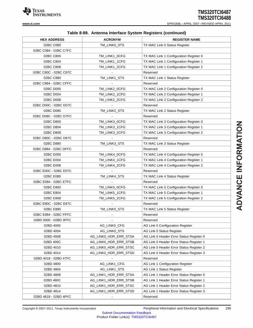
AD
VA
NC
E I
NF
OR
MA
TIO
N
TMS320TCI6487TMS320TCI6488
www.ti.com SPRS358L–APRIL 2007–REVISED APRIL 2011
Table 8-89. Antenna Interface System Registers (continued)
HEX ADDRESS ACRONYM REGISTER NAME
02BC C080 TM_LINK0_STS TX MAC Link 0 Status Register
02BC C084 - 02BC C7FC
02BC C800 TM_LINK1_0CFG TX MAC Link 1 Configuration Register 0
02BC C804 TM_LINK1_1CFG TX MAC Link 1 Configuration Register 1
02BC C808 TM_LINK1_2CFG TX MAC Link 1 Configuration Register 2
02BC C80C - 02BC C87C - Reserved
02BC C880 TM_LINK1_STS TX MAC Link 1 Status Register
02BC C884 - 02BC CFFC - Reserved
02BC D000 TM_LINK2_0CFG TX MAC Link 2 Configuration Register 0
02BC D004 TM_LINK2_1CFG TX MAC Link 2 Configuration Register 1
02BC D008 TM_LINK2_2CFG TX MAC Link 2 Configuration Register 2
02BC D00C - 02BC D07C - Reserved
02BC D080 TM_LINK2_STS TX MAC Link 2 Status Register
02BC D08C - 02BC D7FC - Reserved
02BC D800 TM_LINK3_0CFG TX MAC Link 3 Configuration Register 0
02BC D804 TM_LINK3_1CFG TX MAC Link 3 Configuration Register 1
02BC D808 TM_LINK3_2CFG TX MAC Link 3 Configuration Register 2
02BC D80C - 02BC D87C - Reserved
02BC D880 TM_LINK3_STS TX MAC Link 3 Status Register
02BC D884 - 02BC DFFC - Reserved
02BC E000 TM_LINK4_0CFG TX MAC Link 4 Configuration Register 0
02BC E004 TM_LINK4_1CFG TX MAC Link 4 Configuration Register 1
02BC E008 TM_LINK4_2CFG TX MAC Link 4 Configuration Register 2
02BC E00C - 02BC E07C - Reserved
02BC E080 TM_LINK4_STS TX MAC Link 4 Status Register
02BC E084 - 02BC E7FC - Reserved
02BC E800 TM_LINK5_0CFG TX MAC Link 5 Configuration Register 0
02BC E804 TM_LINK5_1CFG TX MAC Link 5 Configuration Register 1
02BC E808 TM_LINK5_2CFG TX MAC Link 5 Configuration Register 2
02BC E80C - 02BC E87C - Reserved
02BC E880 TM_LINK5_STS TX MAC Link 5 Status Register
02BC E884 - 02BC FFFC - Reserved
02BD 0000 - 02BD 3FFC - Reserved
02BD 4000 AG_LINK0_CFG AG Link 0 Configuration Register
02BD 4004 AG_LINK0_STS AG Link 0 Status Register
02BD 4008 AG_LINK0_HDR_ERR_STSA AG Link 0 Header Error Status Register 0
02BD 400C AG_LINK0_HDR_ERR_STSB AG Link 0 Header Error Status Register 1
02BD 4010 AG_LINK0_HDR_ERR_STSC AG Link 0 Header Error Status Register 2
02BD 4014 AG_LINK0_HDR_ERR_STSD AG Link 0 Header Error Status Register 3
02BD 4018 - 02BD 47FC - Reserved
02BD 4800 AG_LINK1_CFG AG Link 1 Configuration Register
02BD 4804 AG_LINK1_STS AG Link 1 Status Register
02BD 4808 AG_LINK1_HDR_ERR_STSA AG Link 1 Header Error Status Register 0
02BD 480C AG_LINK1_HDR_ERR_STSB AG Link 1 Header Error Status Register 1
02BD 4810 AG_LINK1_HDR_ERR_STSC AG Link 1 Header Error Status Register 2
02BD 4814 AG_LINK1_HDR_ERR_STSD AG Link 1 Header Error Status Register 3
02BD 4818 - 02BD 4FFC - Reserved
Copyright © 2007–2011, Texas Instruments Incorporated Peripheral Information and Electrical Specifications 199Submit Documentation Feedback
Product Folder Link(s): TMS320TCI6487
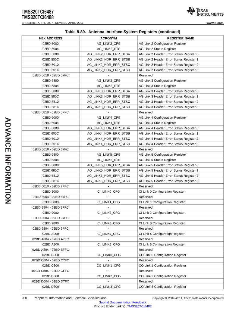
AD
VA
NC
E IN
FO
RM
AT
ION
TMS320TCI6487TMS320TCI6488SPRS358L–APRIL 2007–REVISED APRIL 2011 www.ti.com
Table 8-89. Antenna Interface System Registers (continued)
HEX ADDRESS ACRONYM REGISTER NAME
02BD 5000 AG_LINK2_CFG AG Link 2 Configuration Register
02BD 5004 AG_LINK2_STS AG Link 2 Status Register
02BD 5008 AG_LINK2_HDR_ERR_STSA AG Link 2 Header Error Status Register 0
02BD 500C AG_LINK2_HDR_ERR_STSB AG Link 2 Header Error Status Register 1
02BD 5010 AG_LINK2_HDR_ERR_STSC AG Link 2 Header Error Status Register 2
02BD 5014 AG_LINK2_HDR_ERR_STSD AG Link 2 Header Error Status Register 3
02BD 5018 - 02BD 57FC - Reserved
02BD 5800 AG_LINK3_CFG AG Link 3 Configuration Register
02BD 5804 AG_LINK3_STS AG Link 3 Status Register
02BD 5808 AG_LINK3_HDR_ERR_STSA AG Link 3 Header Error Status Register 0
02BD 580C AG_LINK3_HDR_ERR_STSB AG Link 3 Header Error Status Register 1
02BD 5810 AG_LINK3_HDR_ERR_STSC AG Link 3 Header Error Status Register 2
02BD 5814 AG_LINK3_HDR_ERR_STSD AG Link 3 Header Error Status Register 3
02BD 5818 - 02BD 5FFC - Reserved
02BD 6000 AG_LINK4_CFG AG Link 4 Configuration Register
02BD 6004 AG_LINK4_STS AG Link 4 Status Register
02BD 6008 AG_LINK4_HDR_ERR_STSA AG Link 4 Header Error Status Register 0
02BD 600C AG_LINK4_HDR_ERR_STSB AG Link 4 Header Error Status Register 1
02BD 6010 AG_LINK4_HDR_ERR_STSC AG Link 4 Header Error Status Register 2
02BD 6014 AG_LINK4_HDR_ERR_STSD AG Link 4 Header Error Status Register 3
02BD 6018 - 02BD 67FC - Reserved
02BD 6800 AG_LINK5_CFG AG Link 5 Configuration Register
02BD 6804 AG_LINK5_STS AG Link 5 Status Register
02BD 6808 AG_LINK5_HDR_ERR_STSA AG Link 5 Header Error Status Register 0
02BD 680C AG_LINK5_HDR_ERR_STSB AG Link 5 Header Error Status Register 1
02BD 6810 AG_LINK5_HDR_ERR_STSC AG Link 5 Header Error Status Register 2
02BD 6814 AG_LINK5_HDR_ERR_STSD AG Link 5 Header Error Status Register 3
02BD 6818 - 02BD 7FFC - Reserved
02BD 8000 CI_LINK0_CFG CI Link 0 Configuration Register
02BD 8004 - 02BD 87FC - Reserved
02BD 8800 CI_LINK1_CFG CI Link 1 Configuration Register
02BD 8804 - 02BD 8FFC - Reserved
02BD 9000 CI_LINK2_CFG CI Link 2 Configuration Register
02BD 9004 - 02BD 97FC - Reserved
02BD 9800 CI_LINK3_CFG CI Link 3 Configuration Register
02BD 9804 - 02BD 9FFC - Reserved
02BD A000 CI_LINK4_CFG CI Link 4 Configuration Register
02BD A004 - 02BD A7FC - Reserved
02BD A800 CI_LINK5_CFG CI Link 5 Configuration Register
02BD A804 - 02BD BFFC - Reserved
02BD C000 CO_LINK0_CFG CO Link 0 Configuration Register
02BD C004 - 02BD C7FC - Reserved
02BD C800 CO_LINK1_CFG CO Link 1 Configuration Register
02BD C804 - 02BD CFFC - Reserved
02BD D000 CO_LINK2_CFG CO Link 2 Configuration Register
02BD D004 - 02BD D7FC - Reserved
02BD D800 CO_LINK3_CFG CO Link 3 Configuration Register
200 Peripheral Information and Electrical Specifications Copyright © 2007–2011, Texas Instruments Incorporated
Submit Documentation FeedbackProduct Folder Link(s): TMS320TCI6487

AD
VA
NC
E I
NF
OR
MA
TIO
N
TMS320TCI6487TMS320TCI6488
www.ti.com SPRS358L–APRIL 2007–REVISED APRIL 2011
Table 8-89. Antenna Interface System Registers (continued)
HEX ADDRESS ACRONYM REGISTER NAME
02BD D804 - 02BD DFFC - Reserved
02BD E000 CO_LINK4_CFG CO Link 4 Configuration Register
02BD E004 - 02BD E7FC - Reserved
02BD E800 CO_LINK5_CFG CO Link 5 Configuration Register
02BD E804 - 02BE 3000 - Reserved
02BE 3004 DB_GENERIC_CFG Data Buffer Configuration Register
02BE 3008 DB_DMA_QUE_CLR_CFG Data Buffer DMA Depth Clear Register
02BE 300C DB_DMA_CNT_CLR_CFG Data Buffer DMA Count Clear Register
02BE 3010 DB_OUT_PKTSW_EN_CFG Data Buffer Outbound Packet Switched FIFO EnableRegister
02BE 3014 DB_OUT_PKTSW_FLUSH_CFG Data Buffer Inbound Packet Switched FIFO Flush Register
02BE 3018 DB_IN_FIFO_EVNT_CFG Data Buffer Inbound Packet Switched FIFO Flush Register
02BE 301C DB_IN_FIFO_SIZE_CFG Data Buffer Inbound Packet Switched FIFO DepthRegister
02BE 3020 DB_FORCE_SYSEVENT_CFG Data Buffer Force System Events Register
02BE 3024 DB_OUTB_TRK_AUTOSYNC_CFG Data Buffer PE Tracker Auto Sync Control Register
02BE 3028 DB_INB_TRK_AUTOSYNC_CFG Data Buffer PD Tracker Auto Sync Control Register
02BE 302C - 02BE 303C - Reserved
02BE 3040 DB_IN_DMA_CNT0_STS Data Buffer Inbound DMA Count 0 Register
02BE 3044 DB_IN_DMA_CNT1_STS Data Buffer Inbound DMA Count 1 Register
02BE 3048 DB_IN_DMA_CNT2_STS Data Buffer Inbound DMA Count 2 Register
02BE 304C DB_OUT_DMA_CNT0_STS Data Buffer Outbound DMA Count 0 Register
02BE 3050 DB_OUT_DMA_CNT1_STS Data Buffer Outbound DMA Count 1 Register
02BE 3054 DB_OUT_DMA_CNT2_STS Data Buffer Outbound DMA Count 2 Register
02BE 3058 DB_IN_DMA_DEPTH_STS Data Buffer Inbound DMA Burst Available Register
02BE 305C DB_OUT_DMA_DEPTH_STS Data Buffer Outbound DMA Burst Available Register
02BE 3060 DB_OUT_PKTSW_STS Data Buffer Outbound Packet Switched FIFO StatusRegister
02BE 3064 DB_OUT_PKTSW_DEPTH_STS Data Buffer Outbound Packet Switched FIFO DepthRegister
02BE 3068 DB_OUT_PKTSW_NE_STS Data Buffer Outbound Packet Switched FIFO Not EmptyRegister
02BE 306C - 02BE 307C - Reserved
02BE 3080 DB_OUT_PKTSW_HEAD0_STS Data Buffer Outbound Packet Switched FIFO0 HeadPointer
02BE 3084 DB_OUT_PKTSW_HEAD1_STS Data Buffer Outbound Packet Switched FIFO1 HeadPointer
02BE 3088 DB_OUT_PKTSW_HEAD2_STS Data Buffer Outbound Packet Switched FIFO2 HeadPointer
02BE 308C DB_OUT_PKTSW_HEAD3_STS Data Buffer Outbound Packet Switched FIFO3 HeadPointer
02BE 3090 DB_OUT_PKTSW_HEAD4_STS Data Buffer Outbound Packet Switched FIFO4 HeadPointer
02BE 3094 DB_OUT_PKTSW_HEAD5_STS Data Buffer Outbound Packet Switched FIFO5 HeadPointer
02BE 3098 DB_OUT_PKTSW_HEAD6_STS Data Buffer Outbound Packet Switched FIFO6 HeadPointer
02BE 309C DB_OUT_PKTSW_HEAD7_STS Data Buffer Outbound Packet Switched FIFO7 HeadPointer
02BE 30A0 DB_OUT_PKTSW_HEAD8_STS Data Buffer Outbound Packet Switched FIFO8 HeadPointer
Copyright © 2007–2011, Texas Instruments Incorporated Peripheral Information and Electrical Specifications 201Submit Documentation Feedback
Product Folder Link(s): TMS320TCI6487

AD
VA
NC
E IN
FO
RM
AT
ION
TMS320TCI6487TMS320TCI6488SPRS358L–APRIL 2007–REVISED APRIL 2011 www.ti.com
Table 8-89. Antenna Interface System Registers (continued)
HEX ADDRESS ACRONYM REGISTER NAME
02BE 30A4 DB_OUT_PKTSW_HEAD9_STS Data Buffer Outbound Packet Switched FIFO9 HeadPointer
02BE 30A8 DB_OUT_PKTSW_HEAD10_STS Data Buffer Outbound Packet Switched FIFO10 HeadPointer
02BE 30AC DB_OUT_PKTSW_HEAD11_STS Data Buffer Outbound Packet Switched FIFO11 HeadPointer
02BE 30B0 DB_OUT_PKTSW_HEAD12_STS Data Buffer Outbound Packet Switched FIFO12 HeadPointer
02BE 30B4 DB_OUT_PKTSW_HEAD13_STS Data Buffer Outbound Packet Switched FIFO13 HeadPointer
02BE 30B8 DB_OUT_PKTSW_HEAD14_STS Data Buffer Outbound Packet Switched FIFO14 HeadPointer
02BE 30BC - Reserved
02BE 30C0 DB_OUT_PKTSW_TAIL0_STS Data Buffer Outbound Packet Switched FIFO0 Tail Pointer
02BE 30C4 DB_OUT_PKTSW_TAIL1_STS Data Buffer Outbound Packet Switched FIFO1 Tail Pointer
02BE 30C8 DB_OUT_PKTSW_TAIL2_STS Data Buffer Outbound Packet Switched FIFO2 Tail Pointer
02BE 30CC DB_OUT_PKTSW_TAIL3_STS Data Buffer Outbound Packet Switched FIFO3 Tail Pointer
02BE 30D0 DB_OUT_PKTSW_TAIL4_STS Data Buffer Outbound Packet Switched FIFO4 Tail Pointer
02BE 30D4 DB_OUT_PKTSW_TAIL5_STS Data Buffer Outbound Packet Switched FIFO5 Tail Pointer
02BE 30D8 DB_OUT_PKTSW_TAIL6_STS Data Buffer Outbound Packet Switched FIFO6 Tail Pointer
02BE 30DC DB_OUT_PKTSW_TAIL7_STS Data Buffer Outbound Packet Switched FIFO7 Tail Pointer
02BE 30E0 DB_OUT_PKTSW_TAIL8_STS Data Buffer Outbound Packet Switched FIFO8 Tail Pointer
02BE 30E4 DB_OUT_PKTSW_TAIL9_STS Data Buffer Outbound Packet Switched FIFO9 Tail Pointer
02BE 30E8 DB_OUT_PKTSW_TAIL10_STS Data Buffer Outbound Packet Switched FIFO10 TailPointer
02BE 30EC DB_OUT_PKTSW_TAIL11_STS Data Buffer Outbound Packet Switched FIFO11 TailPointer
02BE 30F0 DB_OUT_PKTSW_TAIL12_STS Data Buffer Outbound Packet Switched FIFO12 TailPointer
02BE 30F4 DB_OUT_PKTSW_TAIL13_STS Data Buffer Outbound Packet Switched FIFO13 TailPointer
02BE 30F8 DB_OUT_PKTSW_TAIL14_STS Data Buffer Outbound Packet Switched FIFO14 TailPointer
02BE 30FC - 02BE 3FFC - Reserved
02BE 4000 PD_LINK0_84CNT_LUT0_CFG PD 84 Count Look-Up Table bits [31:0]
02BE 4004 PD_LINK0_84CNT_LUT1_CFG PD 84 Count Look-Up Table bits [63:32]
02BE 4008 PD_LINK0_84CNT_LUT2_CFG PD 84 Count Look-Up Table bits [83:64]
02BE 400C PD_LINK0_CPRI_SI_LUT0_CFG PD CPRI Stream Index LUT0 Register
02BE 4010 PD_LINK0_CPRI_SI_LUT1_CFG PD CPRI Stream Index LUT1 Register
02BE 4014 - 02BE 47FC - Reserved
02BE 4800 PD_LINK1_84CNT_LUT0_CFG PD 84 Count Look-Up Table bits [31:0]
02BE 4804 PD_LINK1_84CNT_LUT1_CFG PD 84 Count Look-Up Table bits [63:32]
02BE 4808 PD_LINK1_84CNT_LUT2_CFG PD 84 Count Look-Up Table bits [83:64]
02BE 480C PD_LINK1_CPRI_SI_LUT0_CFG PD CPRI Stream Index LUT0 Register
02BE 4810 PD_LINK1_CPRI_SI_LUT1_CFG PD CPRI Stream Index LUT1 Register
02BE 4814 - 02BE 4FFC - Reserved
02BE 5000 PD_LINK2_84CNT_LUT0_CFG PD 84 Count Look-Up Table bits [31:0]
02BE 5004 PD_LINK2_84CNT_LUT1_CFG PD 84 Count Look-Up Table bits [63:32]
02BE 5008 PD_LINK2_84CNT_LUT2_CFG PD 84 Count Look-Up Table bits [83:64]
02BE 500C PD_LINK2_CPRI_SI_LUT0_CFG PD CPRI Stream Index LUT0 Register
02BE 5010 PD_LINK2_CPRI_SI_LUT1_CFG PD CPRI Stream Index LUT1 Register
202 Peripheral Information and Electrical Specifications Copyright © 2007–2011, Texas Instruments Incorporated
Submit Documentation FeedbackProduct Folder Link(s): TMS320TCI6487
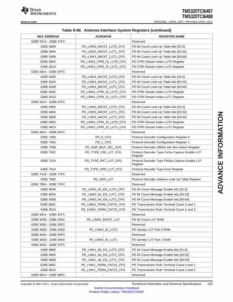
AD
VA
NC
E I
NF
OR
MA
TIO
N
TMS320TCI6487TMS320TCI6488
www.ti.com SPRS358L–APRIL 2007–REVISED APRIL 2011
Table 8-89. Antenna Interface System Registers (continued)
HEX ADDRESS ACRONYM REGISTER NAME
02BE 5014 - 02BE 57FC - Reserved
02BE 5800 PD_LINK3_84CNT_LUT0_CFG PD 84 Count Look-Up Table bits [31:0]
02BE 5804 PD_LINK3_84CNT_LUT1_CFG PD 84 Count Look-Up Table bits [63:32]
02BE 5808 PD_LINK3_84CNT_LUT2_CFG PD 84 Count Look-Up Table bits [83:64]
02BE 580C PD_LINK3_CPRI_SI_LUT0_CFG PD CPRI Stream Index LUT0 Register
02BE 5810 PD_LINK3_CPRI_SI_LUT1_CFG PD CPRI Stream Index LUT1 Register
02BE 5814 - 02BE 5FFC - Reserved
02BE 6000 PD_LINK4_84CNT_LUT0_CFG PD 84 Count Look-Up Table bits [31:0]
02BE 6004 PD_LINK4_84CNT_LUT1_CFG PD 84 Count Look-Up Table bits [63:32]
02BE 6008 PD_LINK4_84CNT_LUT2_CFG PD 84 Count Look-Up Table bits [83:64]
02BE 600C PD_LINK4_CPRI_SI_LUT0_CFG PD CPRI Stream Index LUT0 Register
02BE 6010 PD_LINK4_CPRI_SI_LUT1_CFG PD CPRI Stream Index LUT1 Register
02BE 6014 - 02BE 67FC - Reserved
02BE 6800 PD_LINK5_84CNT_LUT0_CFG PD 84 Count Look-Up Table bits [31:0]
02BE 6804 PD_LINK5_84CNT_LUT1_CFG PD 84 Count Look-Up Table bits [63:32]
02BE 6808 PD_LINK5_84CNT_LUT2_CFG PD 84 Count Look-Up Table bits [83:64]
02BE 680C PD_LINK5_CPRI_SI_LUT0_CFG PD CPRI Stream Index LUT0 Register
02BE 6810 PD_LINK5_CPRI_SI_LUT1_CFG PD CPRI Stream Index LUT1 Register
02BE 6814 - 02BE 6FFC - Reserved
02BE 7000 PD_0_CFG Protocol Decoder Configuration Register 0
02BE 7004 PD_1_CFG Protocol Decoder Configuration Register 1
02BE 7008 PD_ADR_MUX_SEL_CFG Protocol Decoder OBSAI Adr Mux Select Register
02BE 700C PD_TYPE_CIR_LUT_CFG Protocol Decoder Type CirSw Capture Enable LUTRegister
02BE 7010 PD_TYPE_PKT_LUT_CFG Protocol Decoder Type PktSw Capture Enable LUTRegister
02BE 7014 PD_TYPE_ERR_LUT_CFG Protocol Decoder Type Error Register
02BE 7018 - 02BE 77FC - Reserved
02BE 7800 PD_ADR_LUT Protocol Decoder Address Look Up Table Register
02BE 7804 - 02BE 7FFC - Reserved
02BE 8000 PE_LINK0_84_EN_LUT0_CFG PE 84 Count Message Enable bits [31:0]
02BE 8004 PE_LINK0_84_EN_LUT1_CFG PE 84 Count Message Enable bits [63:32]
02BE 8008 PE_LINK0_84_EN_LUT2_CFG PE 84 Count Message Enable bits [83:64]
02BE 800C PE_LINK0_TERM_CNT01_CFG PE Transmission Rule Terminal Count 0 and 1
02BE 8010 PE_LINK0_TERM_CNT23_CFG PE Transmission Rule Terminal Count 2 and 3
02BE 8014 - 02BE 81FC - Reserved
02BE 8200 - 02BE 834C PE_LINK0_84CNT_LUT PE 84 Count LUT RAM
02BE 8350 - 02BE 83FC - Reserved
02BE 8400 - 02BE 8450 PE_LINK0_ID_LUT0 PE Identity LUT Part 0 RAM
02BE 8454 - 02BE 84FC - Reserved
02BE 8500 - 02BE 8550 PE_LINK0_ID_LUT1 PE Identity LUT Part 1 RAM
02BE 8554 - 02BE 87FC - Reserved
02BE 8800 PE_LINK1_84_EN_LUT0_CFG PE 84 Count Message Enable bits [31:0]
02BE 8804 PE_LINK1_84_EN_LUT1_CFG PE 84 Count Message Enable bits [63:32]
02BE 8808 PE_LINK1_84_EN_LUT2_CFG PE 84 Count Message Enable bits [83:64]
02BE 880C PE_LINK1_TERM_CNT01_CFG PE Transmission Rule Terminal Count 0 and 1
02BE 8810 PE_LINK1_TERM_CNT23_CFG PE Transmission Rule Terminal Count 2 and 3
02BE 8814 - 02BE 89FC - Reserved
Copyright © 2007–2011, Texas Instruments Incorporated Peripheral Information and Electrical Specifications 203Submit Documentation Feedback
Product Folder Link(s): TMS320TCI6487

AD
VA
NC
E IN
FO
RM
AT
ION
TMS320TCI6487TMS320TCI6488SPRS358L–APRIL 2007–REVISED APRIL 2011 www.ti.com
Table 8-89. Antenna Interface System Registers (continued)
HEX ADDRESS ACRONYM REGISTER NAME
02BE 8A00 - 02BE 8B4C PE_LINK1_84CNT_LUT PE 84 Count LUT RAM
02BE 8B50 - 02BE 8BFC - Reserved
02BE 8C00 - 02BE 8C50 PE_LINK1_ID_LUT0 PE Identity LUT Part 0 RAM
02BE 8C54 - 02BE 8CFC - Reserved
02BE 8D00 - 02BE 8D50 PE_LINK1_ID_LUT1 PE Identity LUT Part 1 RAM
02BE 8D54 - 02BE 8FFC - Reserved
02BE 9000 PE_LINK2_84_EN_LUT0_CFG PE 84 Count message Enable bits [31: 0]
02BE 9004 PE_LINK2_84_EN_LUT1_CFG PE 84 Count message Enable bits [63 : 32]
02BE 9008 PE_LINK2_84_EN_LUT2_CFG PE 84 Count message Enable bits [83 : 64]
02BE 900C PE_LINK2_TERM_CNT01_CFG PE Transmission Rule Terminal Count 0 and 1
02BE 9010 PE_LINK2_TERM_CNT23_CFG PE Transmission Rule Terminal Count 2 and 3
02BE 9014 - 02BE 91FC - Reserved
02BE 9200 - 02BE 934C PE_LINK2_84CNT_LUT PE 84 Count LUT RAM
02BE 9350 - 02BE 93FC - Reserved
02BE 9400 - 02BE 9450 PE_LINK2_ID_LUT0 PE Identity LUT Part 0 RAM
02BE 9454 - 02BE 94FC - Reserved
02BE 9500 - 02BE 9550 PE_LINK2_ID_LUT1 PE Identity LUT Part 1 RAM
02BE 9554 - 02BE 97FC - Reserved
02BE 9800 PE_LINK3_84_EN_LUT0_CFG PE 84 Count message Enable bits [31:0]
02BE 9804 PE_LINK3_84_EN_LUT1_CFG PE 84 Count message Enable bits [63:32]
02BE 9808 PE_LINK3_84_EN_LUT2_CFG PE 84 Count message Enable bits [83:64]
02BE 980C PE_LINK3_TERM_CNT01_CFG PE Transmission Rule Terminal Count 0 and 1
02BE 9810 PE_LINK3_TERM_CNT23_CFG PE Transmission Rule Terminal Count 2 and 3
02BE 9814 - 02BE 99FC - Reserved
02BE 9A00 - 02BE 9B4C PE_LINK3_84CNT_LUT PE 84 Count LUT RAM
02BE 9B50 - 02BE 9BFC - Reserved
02BE 9C00 - 02BE 9C50 PE_LINK3_ID_LUT0 PE Identity LUT Part 0 RAM
02BE 9C54 - 02BE 9CFC - Reserved
02BE 9D00 - 02BE 9D50 PE_LINK3_ID_LUT1 PE Identity LUT Part 1 RAM
02BE 9D54 - 02BE 9FFC - Reserved
02BE A000 PE_LINK4_84_EN_LUT0_CFG PE 84 Count Message Enable bits [31:0]
02BE A004 PE_LINK4_84_EN_LUT1_CFG PE 84 Count Message Enable bits [63:32]
02BE A008 PE_LINK4_84_EN_LUT2_CFG PE 84 Count Message Enable bits [83:64]
02BE A00C PE_LINK4_TERM_CNT01_CFG PE Transmission Rule Terminal Count 0 and 1
02BE A010 PE_LINK4_TERM_CNT23_CFG PE Transmission Rule Terminal Count 2 and 3
02BE A014 - 02BE A1FC - Reserved
02BE A200 - 02BE A34C PE_LINK4_84CNT_LUT PE 84 Count LUT RAM
02BE A350 - 02BE A3FC - Reserved
02BE A400 - 02BE A450 PE_LINK4_ID_LUT0 PE Identity LUT Part 0 RAM
02BE A454 - 02BE A4FC - Reserved
02BE A500 - 02BE A550 PE_LINK4_ID_LUT1 PE Identity LUT Part 1 RAM
02BE A554 - 02BE A7FC - Reserved
02BE A800 PE_LINK5_84_EN_LUT0_CFG PE 84 Count Message Enable bits [31:0]
02BE A804 PE_LINK5_84_EN_LUT1_CFG PE 84 Count Message Enable bits [63:32]
02BE A808 PE_LINK5_84_EN_LUT2_CFG PE 84 Count Message Enable bits [83:64]
02BE A80C PE_LINK5_TERM_CNT01_CFG PE Transmission Rule Terminal Count 0 and 1
02BE A810 PE_LINK5_TERM_CNT23_CFG PE Transmission Rule Terminal Count 2 and 3
204 Peripheral Information and Electrical Specifications Copyright © 2007–2011, Texas Instruments Incorporated
Submit Documentation FeedbackProduct Folder Link(s): TMS320TCI6487
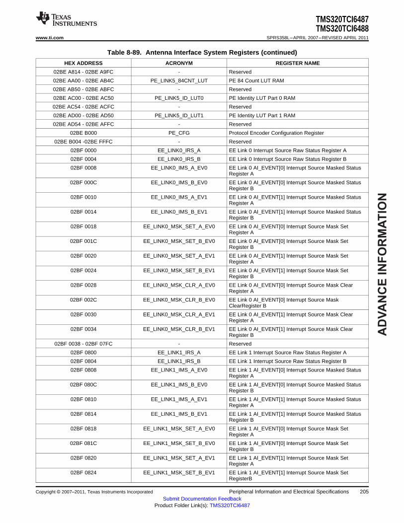
AD
VA
NC
E I
NF
OR
MA
TIO
N
TMS320TCI6487TMS320TCI6488
www.ti.com SPRS358L–APRIL 2007–REVISED APRIL 2011
Table 8-89. Antenna Interface System Registers (continued)
HEX ADDRESS ACRONYM REGISTER NAME
02BE A814 - 02BE A9FC - Reserved
02BE AA00 - 02BE AB4C PE_LINK5_84CNT_LUT PE 84 Count LUT RAM
02BE AB50 - 02BE ABFC - Reserved
02BE AC00 - 02BE AC50 PE_LINK5_ID_LUT0 PE Identity LUT Part 0 RAM
02BE AC54 - 02BE ACFC - Reserved
02BE AD00 - 02BE AD50 PE_LINK5_ID_LUT1 PE Identity LUT Part 1 RAM
02BE AD54 - 02BE AFFC - Reserved
02BE B000 PE_CFG Protocol Encoder Configuration Register
02BE B004 -02BE FFFC - Reserved
02BF 0000 EE_LINK0_IRS_A EE Link 0 Interrupt Source Raw Status Register A
02BF 0004 EE_LINK0_IRS_B EE Link 0 Interrupt Source Raw Status Register B
02BF 0008 EE_LINK0_IMS_A_EV0 EE Link 0 AI_EVENT[0] Interrupt Source Masked StatusRegister A
02BF 000C EE_LINK0_IMS_B_EV0 EE Link 0 AI_EVENT[0] Interrupt Source Masked StatusRegister B
02BF 0010 EE_LINK0_IMS_A_EV1 EE Link 0 AI_EVENT[1] Interrupt Source Masked StatusRegister A
02BF 0014 EE_LINK0_IMS_B_EV1 EE Link 0 AI_EVENT[1] Interrupt Source Masked StatusRegister B
02BF 0018 EE_LINK0_MSK_SET_A_EV0 EE Link 0 AI_EVENT[0] Interrupt Source Mask SetRegister A
02BF 001C EE_LINK0_MSK_SET_B_EV0 EE Link 0 AI_EVENT[0] Interrupt Source Mask SetRegister B
02BF 0020 EE_LINK0_MSK_SET_A_EV1 EE Link 0 AI_EVENT[1] Interrupt Source Mask SetRegister A
02BF 0024 EE_LINK0_MSK_SET_B_EV1 EE Link 0 AI_EVENT[1] Interrupt Source Mask SetRegister B
02BF 0028 EE_LINK0_MSK_CLR_A_EV0 EE Link 0 AI_EVENT[0] Interrupt Source Mask ClearRegister A
02BF 002C EE_LINK0_MSK_CLR_B_EV0 EE Link 0 AI_EVENT[0] Interrupt Source MaskClearRegister B
02BF 0030 EE_LINK0_MSK_CLR_A_EV1 EE Link 0 AI_EVENT[1] Interrupt Source Mask ClearRegister A
02BF 0034 EE_LINK0_MSK_CLR_B_EV1 EE Link 0 AI_EVENT[1] Interrupt Source Mask ClearRegister B
02BF 0038 - 02BF 07FC - Reserved
02BF 0800 EE_LINK1_IRS_A EE Link 1 Interrupt Source Raw Status Register A
02BF 0804 EE_LINK1_IRS_B EE Link 1 Interrupt Source Raw Status Register B
02BF 0808 EE_LINK1_IMS_A_EV0 EE Link 1 AI_EVENT[0] Interrupt Source Masked StatusRegister A
02BF 080C EE_LINK1_IMS_B_EV0 EE Link 1 AI_EVENT[0] Interrupt Source Masked StatusRegister B
02BF 0810 EE_LINK1_IMS_A_EV1 EE Link 1 AI_EVENT[1] Interrupt Source Masked StatusRegister A
02BF 0814 EE_LINK1_IMS_B_EV1 EE Link 1 AI_EVENT[1] Interrupt Source Masked StatusRegister B
02BF 0818 EE_LINK1_MSK_SET_A_EV0 EE Link 1 AI_EVENT[0] Interrupt Source Mask SetRegister A
02BF 081C EE_LINK1_MSK_SET_B_EV0 EE Link 1 AI_EVENT[0] Interrupt Source Mask SetRegister B
02BF 0820 EE_LINK1_MSK_SET_A_EV1 EE Link 1 AI_EVENT[1] Interrupt Source Mask SetRegister A
02BF 0824 EE_LINK1_MSK_SET_B_EV1 EE Link 1 AI_EVENT[1] Interrupt Source Mask SetRegisterB
Copyright © 2007–2011, Texas Instruments Incorporated Peripheral Information and Electrical Specifications 205Submit Documentation Feedback
Product Folder Link(s): TMS320TCI6487
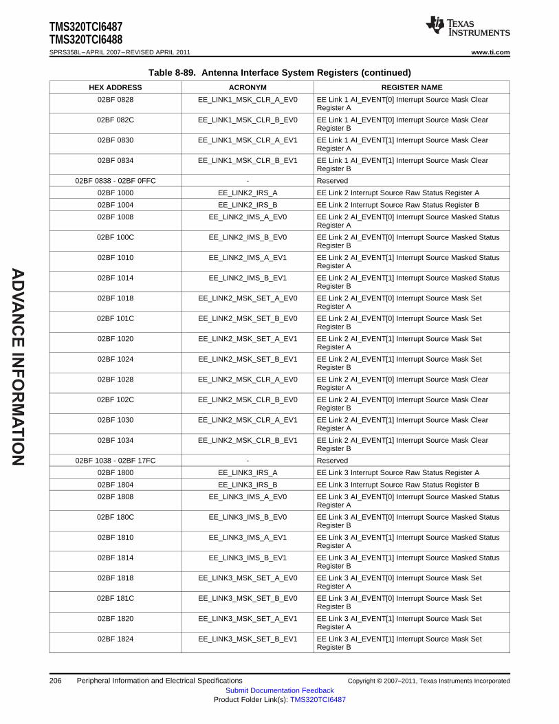
AD
VA
NC
E IN
FO
RM
AT
ION
TMS320TCI6487TMS320TCI6488SPRS358L–APRIL 2007–REVISED APRIL 2011 www.ti.com
Table 8-89. Antenna Interface System Registers (continued)
HEX ADDRESS ACRONYM REGISTER NAME
02BF 0828 EE_LINK1_MSK_CLR_A_EV0 EE Link 1 AI_EVENT[0] Interrupt Source Mask ClearRegister A
02BF 082C EE_LINK1_MSK_CLR_B_EV0 EE Link 1 AI_EVENT[0] Interrupt Source Mask ClearRegister B
02BF 0830 EE_LINK1_MSK_CLR_A_EV1 EE Link 1 AI_EVENT[1] Interrupt Source Mask ClearRegister A
02BF 0834 EE_LINK1_MSK_CLR_B_EV1 EE Link 1 AI_EVENT[1] Interrupt Source Mask ClearRegister B
02BF 0838 - 02BF 0FFC - Reserved
02BF 1000 EE_LINK2_IRS_A EE Link 2 Interrupt Source Raw Status Register A
02BF 1004 EE_LINK2_IRS_B EE Link 2 Interrupt Source Raw Status Register B
02BF 1008 EE_LINK2_IMS_A_EV0 EE Link 2 AI_EVENT[0] Interrupt Source Masked StatusRegister A
02BF 100C EE_LINK2_IMS_B_EV0 EE Link 2 AI_EVENT[0] Interrupt Source Masked StatusRegister B
02BF 1010 EE_LINK2_IMS_A_EV1 EE Link 2 AI_EVENT[1] Interrupt Source Masked StatusRegister A
02BF 1014 EE_LINK2_IMS_B_EV1 EE Link 2 AI_EVENT[1] Interrupt Source Masked StatusRegister B
02BF 1018 EE_LINK2_MSK_SET_A_EV0 EE Link 2 AI_EVENT[0] Interrupt Source Mask SetRegister A
02BF 101C EE_LINK2_MSK_SET_B_EV0 EE Link 2 AI_EVENT[0] Interrupt Source Mask SetRegister B
02BF 1020 EE_LINK2_MSK_SET_A_EV1 EE Link 2 AI_EVENT[1] Interrupt Source Mask SetRegister A
02BF 1024 EE_LINK2_MSK_SET_B_EV1 EE Link 2 AI_EVENT[1] Interrupt Source Mask SetRegister B
02BF 1028 EE_LINK2_MSK_CLR_A_EV0 EE Link 2 AI_EVENT[0] Interrupt Source Mask ClearRegister A
02BF 102C EE_LINK2_MSK_CLR_B_EV0 EE Link 2 AI_EVENT[0] Interrupt Source Mask ClearRegister B
02BF 1030 EE_LINK2_MSK_CLR_A_EV1 EE Link 2 AI_EVENT[1] Interrupt Source Mask ClearRegister A
02BF 1034 EE_LINK2_MSK_CLR_B_EV1 EE Link 2 AI_EVENT[1] Interrupt Source Mask ClearRegister B
02BF 1038 - 02BF 17FC - Reserved
02BF 1800 EE_LINK3_IRS_A EE Link 3 Interrupt Source Raw Status Register A
02BF 1804 EE_LINK3_IRS_B EE Link 3 Interrupt Source Raw Status Register B
02BF 1808 EE_LINK3_IMS_A_EV0 EE Link 3 AI_EVENT[0] Interrupt Source Masked StatusRegister A
02BF 180C EE_LINK3_IMS_B_EV0 EE Link 3 AI_EVENT[0] Interrupt Source Masked StatusRegister B
02BF 1810 EE_LINK3_IMS_A_EV1 EE Link 3 AI_EVENT[1] Interrupt Source Masked StatusRegister A
02BF 1814 EE_LINK3_IMS_B_EV1 EE Link 3 AI_EVENT[1] Interrupt Source Masked StatusRegister B
02BF 1818 EE_LINK3_MSK_SET_A_EV0 EE Link 3 AI_EVENT[0] Interrupt Source Mask SetRegister A
02BF 181C EE_LINK3_MSK_SET_B_EV0 EE Link 3 AI_EVENT[0] Interrupt Source Mask SetRegister B
02BF 1820 EE_LINK3_MSK_SET_A_EV1 EE Link 3 AI_EVENT[1] Interrupt Source Mask SetRegister A
02BF 1824 EE_LINK3_MSK_SET_B_EV1 EE Link 3 AI_EVENT[1] Interrupt Source Mask SetRegister B
206 Peripheral Information and Electrical Specifications Copyright © 2007–2011, Texas Instruments Incorporated
Submit Documentation FeedbackProduct Folder Link(s): TMS320TCI6487

AD
VA
NC
E I
NF
OR
MA
TIO
N
TMS320TCI6487TMS320TCI6488
www.ti.com SPRS358L–APRIL 2007–REVISED APRIL 2011
Table 8-89. Antenna Interface System Registers (continued)
HEX ADDRESS ACRONYM REGISTER NAME
02BF 1828 EE_LINK3_MSK_CLR_A_EV0 EE Link 3 AI_EVENT[0] Interrupt Source Mask ClearRegister A
02BF 182C EE_LINK3_MSK_CLR_B_EV0 EE Link 3 AI_EVENT[0] Interrupt Source Mask ClearRegister B
02BF 1830 EE_LINK3_MSK_CLR_A_EV1 EE Link 3 AI_EVENT[1] Interrupt Source Mask ClearRegister A
02BF 1834 EE_LINK3_MSK_CLR_B_EV1 EE Link 3 AI_EVENT[1] Interrupt Source Mask ClearRegister B
02BF 1838 - 02BF 1FFC - Reserved
02BF 2000 EE_LINK4_IRS_A EE Link 4 Interrupt Source Raw Status Register A
02BF 2004 EE_LINK4_IRS_B EE Link 4 Interrupt Source Raw Status Register B
02BF 2008 EE_LINK4_IMS_A_EV0 EE Link 4 AI_EVENT[0] Interrupt Source Masked StatusRegister A
02BF 200C EE_LINK4_IMS_B_EV0 EE Link 4 AI_EVENT[0] Interrupt Source Masked StatusRegister B
02BF 2010 EE_LINK4_IMS_A_EV1 EE Link 4 AI_EVENT[1] Interrupt Source Masked StatusRegister A
02BF 2014 EE_LINK4_IMS_B_EV1 EE Link 4 AI_EVENT[1] Interrupt Source Masked StatusRegister B
02BF 2018 EE_LINK4_MSK_SET_A_EV0 EE Link 4 AI_EVENT[0] Interrupt Source Mask SetRegister A
02BF 201C EE_LINK4_MSK_SET_B_EV0 EE Link 4 AI_EVENT[0] Interrupt Source Mask SetRegister B
02BF 2020 EE_LINK4_MSK_SET_A_EV1 EE Link 4 AI_EVENT[1] Interrupt Source Mask SetRegister A
02BF 2024 EE_LINK4_MSK_SET_B_EV1 EE Link 4 AI_EVENT[1] Interrupt Source Mask SetRegister B
02BF 2028 EE_LINK4_MSK_CLR_A_EV0 EE Link 4 AI_EVENT[0] Interrupt Source Mask ClearRegister A
02BF 202C EE_LINK4_MSK_CLR_B_EV0 EE Link 4 AI_EVENT[0] Interrupt Source Mask ClearRegister B
02BF 2030 EE_LINK4_MSK_CLR_A_EV1 EE Link 4 AI_EVENT[1] Interrupt Source Mask ClearRegister A
02BF 2034 EE_LINK4_MSK_CLR_B_EV1 EE Link 4 AI_EVENT[1] Interrupt Source Mask ClearRegister B
02BF 2038 - 02BF 27FC - Reserved
02BF 2800 EE_LINK5_IRS_A EE Link 5 Interrupt Source Raw Status Register A
02BF 2804 EE_LINK5_IRS_B EE Link 5 Interrupt Source Raw Status Register B
02BF 2808 EE_LINK5_IMS_A_EV0 EE Link 5 AI_EVENT[0] Interrupt Source Masked StatusRegister A
02BF 280C EE_LINK5_IMS_B_EV0 EE Link 5 AI_EVENT[0] Interrupt Source Masked StatusRegister B
02BF 2810 EE_LINK5_IMS_A_EV1 EE Link 5 AI_EVENT[1] Interrupt Source Masked StatusRegister A
02BF 2814 EE_LINK5_IMS_B_EV1 EE Link 5 AI_EVENT[1] Interrupt Source Masked StatusRegister B
02BF 2818 EE_LINK5_MSK_SET_A_EV0 EE Link 5 AI_EVENT[0] Interrupt Source Mask SetRegister A
02BF 281C EE_LINK5_MSK_SET_B_EV0 EE Link 5 AI_EVENT[0] Interrupt Source Mask SetRegisterB
02BF 2820 EE_LINK5_MSK_SET_A_EV1 EE Link 5 AI_EVENT[1] Interrupt Source Mask SetRegisterA
02BF 2824 EE_LINK5_MSK_SET_B_EV1 EE Link 5 AI_EVENT[1] Interrupt Source Mask SetRegister B
Copyright © 2007–2011, Texas Instruments Incorporated Peripheral Information and Electrical Specifications 207Submit Documentation Feedback
Product Folder Link(s): TMS320TCI6487
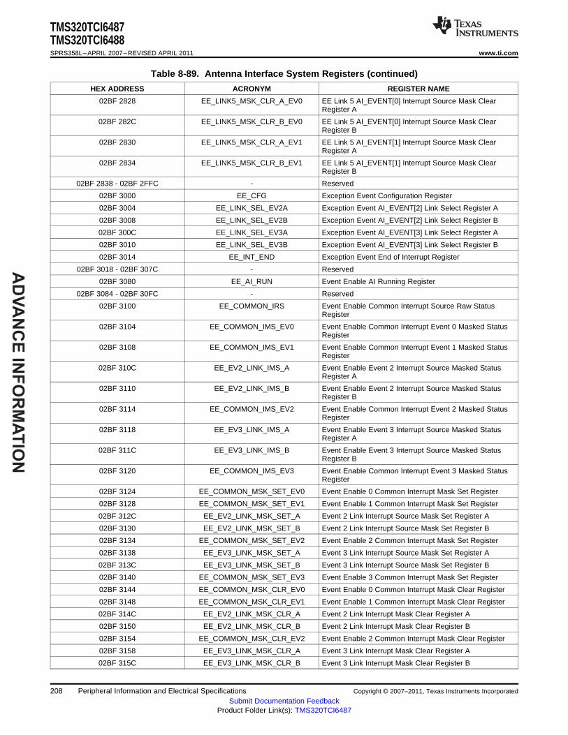
AD
VA
NC
E IN
FO
RM
AT
ION
TMS320TCI6487TMS320TCI6488SPRS358L–APRIL 2007–REVISED APRIL 2011 www.ti.com
Table 8-89. Antenna Interface System Registers (continued)
HEX ADDRESS ACRONYM REGISTER NAME
02BF 2828 EE_LINK5_MSK_CLR_A_EV0 EE Link 5 AI_EVENT[0] Interrupt Source Mask ClearRegister A
02BF 282C EE_LINK5_MSK_CLR_B_EV0 EE Link 5 AI_EVENT[0] Interrupt Source Mask ClearRegister B
02BF 2830 EE_LINK5_MSK_CLR_A_EV1 EE Link 5 AI_EVENT[1] Interrupt Source Mask ClearRegister A
02BF 2834 EE_LINK5_MSK_CLR_B_EV1 EE Link 5 AI_EVENT[1] Interrupt Source Mask ClearRegister B
02BF 2838 - 02BF 2FFC - Reserved
02BF 3000 EE_CFG Exception Event Configuration Register
02BF 3004 EE_LINK_SEL_EV2A Exception Event AI_EVENT[2] Link Select Register A
02BF 3008 EE_LINK_SEL_EV2B Exception Event AI_EVENT[2] Link Select Register B
02BF 300C EE_LINK_SEL_EV3A Exception Event AI_EVENT[3] Link Select Register A
02BF 3010 EE_LINK_SEL_EV3B Exception Event AI_EVENT[3] Link Select Register B
02BF 3014 EE_INT_END Exception Event End of Interrupt Register
02BF 3018 - 02BF 307C - Reserved
02BF 3080 EE_AI_RUN Event Enable AI Running Register
02BF 3084 - 02BF 30FC - Reserved
02BF 3100 EE_COMMON_IRS Event Enable Common Interrupt Source Raw StatusRegister
02BF 3104 EE_COMMON_IMS_EV0 Event Enable Common Interrupt Event 0 Masked StatusRegister
02BF 3108 EE_COMMON_IMS_EV1 Event Enable Common Interrupt Event 1 Masked StatusRegister
02BF 310C EE_EV2_LINK_IMS_A Event Enable Event 2 Interrupt Source Masked StatusRegister A
02BF 3110 EE_EV2_LINK_IMS_B Event Enable Event 2 Interrupt Source Masked StatusRegister B
02BF 3114 EE_COMMON_IMS_EV2 Event Enable Common Interrupt Event 2 Masked StatusRegister
02BF 3118 EE_EV3_LINK_IMS_A Event Enable Event 3 Interrupt Source Masked StatusRegister A
02BF 311C EE_EV3_LINK_IMS_B Event Enable Event 3 Interrupt Source Masked StatusRegister B
02BF 3120 EE_COMMON_IMS_EV3 Event Enable Common Interrupt Event 3 Masked StatusRegister
02BF 3124 EE_COMMON_MSK_SET_EV0 Event Enable 0 Common Interrupt Mask Set Register
02BF 3128 EE_COMMON_MSK_SET_EV1 Event Enable 1 Common Interrupt Mask Set Register
02BF 312C EE_EV2_LINK_MSK_SET_A Event 2 Link Interrupt Source Mask Set Register A
02BF 3130 EE_EV2_LINK_MSK_SET_B Event 2 Link Interrupt Source Mask Set Register B
02BF 3134 EE_COMMON_MSK_SET_EV2 Event Enable 2 Common Interrupt Mask Set Register
02BF 3138 EE_EV3_LINK_MSK_SET_A Event 3 Link Interrupt Source Mask Set Register A
02BF 313C EE_EV3_LINK_MSK_SET_B Event 3 Link Interrupt Source Mask Set Register B
02BF 3140 EE_COMMON_MSK_SET_EV3 Event Enable 3 Common Interrupt Mask Set Register
02BF 3144 EE_COMMON_MSK_CLR_EV0 Event Enable 0 Common Interrupt Mask Clear Register
02BF 3148 EE_COMMON_MSK_CLR_EV1 Event Enable 1 Common Interrupt Mask Clear Register
02BF 314C EE_EV2_LINK_MSK_CLR_A Event 2 Link Interrupt Mask Clear Register A
02BF 3150 EE_EV2_LINK_MSK_CLR_B Event 2 Link Interrupt Mask Clear Register B
02BF 3154 EE_COMMON_MSK_CLR_EV2 Event Enable 2 Common Interrupt Mask Clear Register
02BF 3158 EE_EV3_LINK_MSK_CLR_A Event 3 Link Interrupt Mask Clear Register A
02BF 315C EE_EV3_LINK_MSK_CLR_B Event 3 Link Interrupt Mask Clear Register B
208 Peripheral Information and Electrical Specifications Copyright © 2007–2011, Texas Instruments Incorporated
Submit Documentation FeedbackProduct Folder Link(s): TMS320TCI6487

AD
VA
NC
E I
NF
OR
MA
TIO
N
TMS320TCI6487TMS320TCI6488
www.ti.com SPRS358L–APRIL 2007–REVISED APRIL 2011
Table 8-89. Antenna Interface System Registers (continued)
HEX ADDRESS ACRONYM REGISTER NAME
02BF 3160 EE_COMMON_MSK_CLR_EV3 Event Enable 3 Common Interrupt Mask Clear Register
02BF 3164 - 02BF 31FC - Reserved
02BF 3200 EE_INT_VECT_EV0 Event Enable Interrupt Vector Register for AI_EVENT0
02BF 3204 EE_INT_VECT_EV1 Event Enable Interrupt Vector Register for AI_EVENT1
02BF 3208 EE_INT_VECT_EV2 Event Enable Interrupt Vector Register for AI_EVENT2
02BF 320C EE_INT_VECT_EV3 Event Enable Interrupt Vector Register for AI_EVENT3
02BF 3210 - 02BF BFFC - Reserved
02BF C000 VD_RD_BUSERR VBUSP DMA Read Bus Interface Status Registers
02BF C004 VD_WR_BUSERR VBUSP DMA Write Bus Interface Status Registers
8.22.2 Antenna Electrical Data/Timing
The TMS320TCI6487/88 Hardware Design Guide application report (literature number SPRAAG5)specifies a complete AIF interface solution for the TCI6487/8 device as well as a list of compatible AIFdevices. TI has performed the simulation and system characterization to ensure all AIF interface timings inthis solution are met; therefore, no electrical data/timing information is supplied here for this interface.
TI only supports designs that follow the board design guidelines outlined in the SPRAAG5application report.
Copyright © 2007–2011, Texas Instruments Incorporated Peripheral Information and Electrical Specifications 209Submit Documentation Feedback
Product Folder Link(s): TMS320TCI6487

AD
VA
NC
E IN
FO
RM
AT
ION
TMS320TCI6487TMS320TCI6488SPRS358L–APRIL 2007–REVISED APRIL 2011 www.ti.com
8.23 Frame Synchronization
Frame synchronization handles timing and time alignment on the device by coordinating timing betweenthe DSP cores. Up to 30 programmable events based on RP3 or system timer. One output is used forexporting frame alignment to aid in synchronizing external components.
Frame synchronization assists with synchronization of clock inputs:• OBSAI RP1 compliant input for frame burst data.• UMTS frame synchronization boundary used as an alternative to RP1 for frame burst data.• System timer synchronization used as an alternative to RP1.
The user may select between the OBSAI RP1-compliant FSYNCCLK(P|N) and FRAMEBURST(P|N)signals or the alternate, single-ended ALTFSYNCCLK and ALTFSYNCPULSE inputs to drive the timers.
Table 8-90. FSYNC Event Connections
C64x+ C64x+ C64x+MODULE EVENTS MEGAMODULE MEGAMODULE MEGAMODULE CIC0 CIC1 CIC2 TPCC CIC3 TIMER AIF RAC
CORE 0 CORE 1 CORE 2
FSEVT0 X X X X
FSEVT1 X X X X X
FSEVT2 X X X X X
FSEVT3 X X X X X
FSEVT4 X X X X X
FSEVT5 X X X X
FSEVT6 X X X X
FSEVT7 X X X X
FSEVT8 X X X X
FSEVT9 X X X X
FSEVT10 X X X X
FSEVT11 X X X X
FSEVT12 X X X X
FSEVT13 X X X X
FSEVT14 X X X X
FSEVT15 X X X X
FSEVT16 X X X X
FSEVT17 X X X X
FSEVT18 X X X X X
FSEVT19 X X X X X
FSEVT20 X X X X X
FSEVT21 X X X X X
FSEVT22 X X X X X
FSEVT23 X X X X X
FSEVT24 X X X X
FSEVT25 X X X X
FSEVT26 X X X X
FSEVT27 X X X X
FSEVT28 X X X X
FSEVT29 X X X X
FS_ERR_Alarm0 X X X
FS_ERR_Alarm1 X X X
FS_AIFFrameSync X
210 Peripheral Information and Electrical Specifications Copyright © 2007–2011, Texas Instruments Incorporated
Submit Documentation FeedbackProduct Folder Link(s): TMS320TCI6487

AD
VA
NC
E I
NF
OR
MA
TIO
N
TMS320TCI6487TMS320TCI6488
www.ti.com SPRS358L–APRIL 2007–REVISED APRIL 2011
8.23.1 Frame Synchronization (FSYNC) Register Description(s)
Table 8-91. Frame Synchronization (FSYNC) Registers
HEX ADDRESS ACRONYM REGISTER NAME
0280 0000 PID Peripheral Identification Register
0280 00A0 ERR_INT_MASK_1 FSYNC ERR INT MASK 1 Register
0280 00A4 ERR_INT_SET FSYNC ERR INT SET Register
0280 00A8 ERR_INT_CLEAR FSYNC ERR INT CLEAR Register
0280 00AC ERR_END_OF_INT FSYNC ERR END 0F INT Register
0280 00B0 SCRATCH FSYNC Scratch Register
0280 00B4 CTL1 FSYNC Control Register 1
0280 00B8 CTL2 FSYNC Control Register 2
0280 00BC EMUCTL FSYNC Emulation Control Register
0280 00C0 EMUMASK FSYNC Emulation Mask Register
0280 00C4 RP1TS FSYNC RP1 Type Select Register
0280 00C8 UPDATE FSYNC Update Register
0280 00CC RP3INIT FSYNC RP3 Init Register
0280 00D0 SYSINIT FSYNC System Init Register
0280 0080 ERR_INT_SRC_RAW FSYNC ERR INT SRC RAW Register
0280 0084 ERR_MASK_STAT_0 FSYNC ERR MASK STATUS 0 Register
0280 0088 ERR_MASK_STAT_1 FSYNC ERR MASK STATUS 1 Register
0280 008C ERR_SET_MASK_0 FSYNC ERR SET MASK 0 Register
0280 0090 ERR_SET_MASK_1 FSYNC ERR SET MASK 1 Register
0280 0094 ERR_CLEAR_MASK_0 FSYNC ERR CLEAR MASK 0 Register
0280 0098 ERR_CLEAR_MASK_1 FSYNC ERR CLEAR MASK 1 Register
0280 009C ERR_INT_MASK_0 FSYNC ERR INT MASK 0 Register
0280 0100 RP3TC FSYNC RP3 Terminal Count Entry
0280 0128 TOD1 FSYNC TOD Capture Register 1
0280 012C FSYNC_TOD2 FSYNC TOD Capture Register 2
0280 0130 RP31 FSYNC RP3 Capture Register 1
0280 0134 RP32 FSYNC RP3 Capture Register 2
0280 0138 SYS1 FSYNC SYS Capture Register 1
0280 013C SYS2 FSYNC SYS Capture Register 2
0280 0140 SYSTC_RAM FSYNC System Terminal Count Entry
0280 0168 SYSTC FSYNC System Terminal Count Register
0280 016C RP3TC FSYNC RP3 Terminal Count Register
0280 0170 TYPE FSYNC Type Capture Register
0280 0174 TODVAL FSYNC TOD VAL Register
0280 0178 RP3VAL FSYNC RP3 VAL Register
0280 017C SYSVAL FSYNC System VAL Register
0280 0200 EGMCTRL FSYNC Mask Event Generator Control Register
0280 0258 EGCCTRL FSYNC Counter Event Generator Control Register
0280 0280 EGMMASK FSYNC Mask Event Generator Mask
0280 0300 EGMOFFSET FSYNC Mask Event Generator Offset Value
0280 0358 EGMCTCOUNT FSYNC Counter Event Generator Control Register
0280 0380 EVTFORCE FSYNC Event Force Register
Copyright © 2007–2011, Texas Instruments Incorporated Peripheral Information and Electrical Specifications 211Submit Documentation Feedback
Product Folder Link(s): TMS320TCI6487
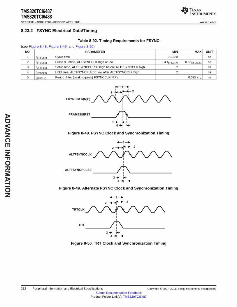
AD
VA
NC
E IN
FO
RM
AT
ION
2 2
1
34
FSYNCCLK(N|P)
FRAMEBURST
2 2
1
3
4
ALTFSYNCCLK
ALTFSYNCPULSE
2 2
1
3
4
TRTCLK
TRT
TMS320TCI6487TMS320TCI6488SPRS358L–APRIL 2007–REVISED APRIL 2011 www.ti.com
8.23.2 FSYNC Electrical Data/Timing
Table 8-92. Timing Requirements for FSYNC(see Figure 8-48, Figure 8-49, and Figure 8-50)
NO. PARAMETER MIN MAX UNIT
1 tc(FSCLK) Cycle time 8.1388 ns
2 tc(FSCLK) Pulse duration, ALTSYNCCLK high or low 0.4 tc(FSCLK) 0.6 tc(FSCLK) ns
3 tu(FSPLS) Setup time, ALTFSYNCPULSE high before ALTFSYNCCLK high 2 ns
4 th(FSPLS) Hold time, ALTFSYNCPULSE low after ALTFSYNCCLK high 2 ns
5 tj(FSCLK) Period Jitter (peak-to-peak) FSYNCCLK(N|P) 0.025 x tc ns
Figure 8-48. FSYNC Clock and Synchronization Timing
Figure 8-49. Alternate FSYNC Clock and Synchronization Timing
Figure 8-50. TRT Clock and Synchronization Timing
212 Peripheral Information and Electrical Specifications Copyright © 2007–2011, Texas Instruments Incorporated
Submit Documentation FeedbackProduct Folder Link(s): TMS320TCI6487
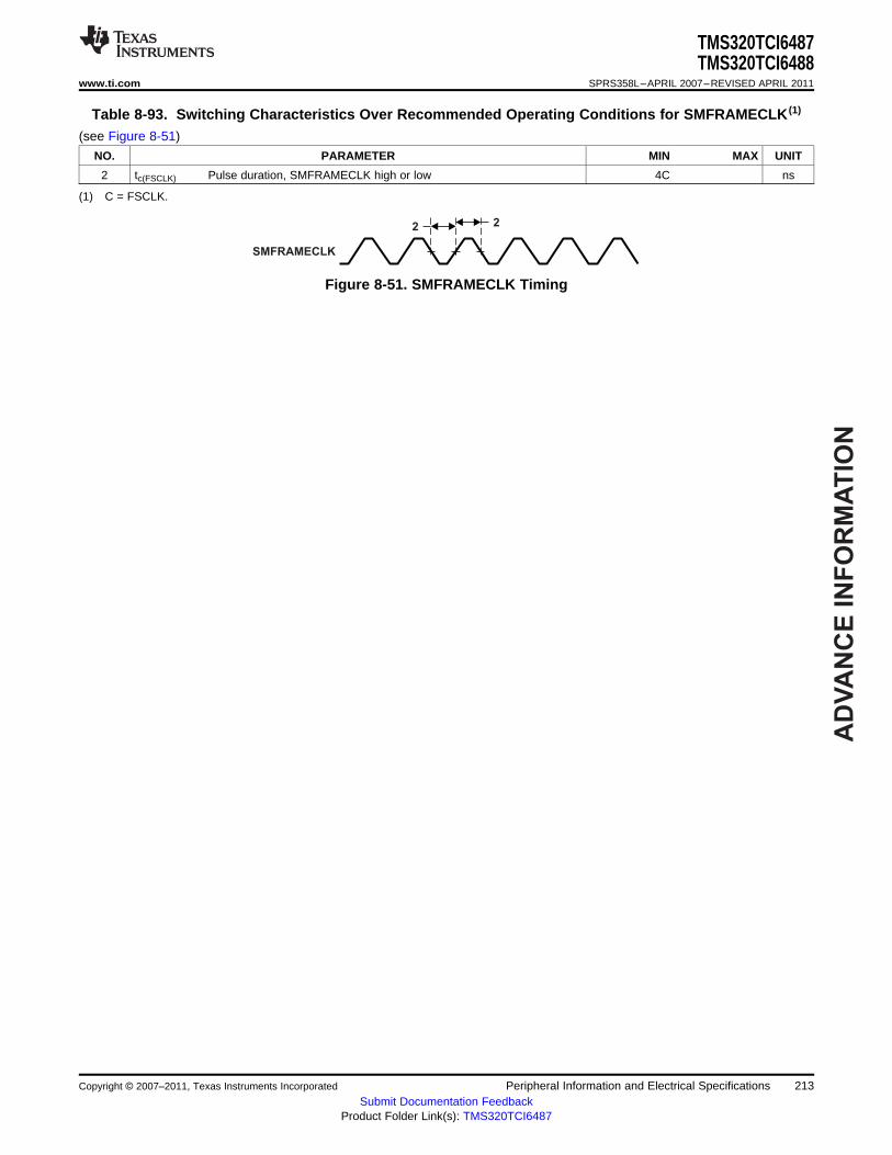
AD
VA
NC
E I
NF
OR
MA
TIO
N
2 2
SMFRAMECLK
TMS320TCI6487TMS320TCI6488
www.ti.com SPRS358L–APRIL 2007–REVISED APRIL 2011
Table 8-93. Switching Characteristics Over Recommended Operating Conditions for SMFRAMECLK (1)
(see Figure 8-51)
NO. PARAMETER MIN MAX UNIT
2 tc(FSCLK) Pulse duration, SMFRAMECLK high or low 4C ns
(1) C = FSCLK.
Figure 8-51. SMFRAMECLK Timing
Copyright © 2007–2011, Texas Instruments Incorporated Peripheral Information and Electrical Specifications 213Submit Documentation Feedback
Product Folder Link(s): TMS320TCI6487
AD
VA
NC
E IN
FO
RM
AT
ION
TMS320TCI6487TMS320TCI6488SPRS358L–APRIL 2007–REVISED APRIL 2011 www.ti.com
8.24 RAC (TCI6488 Only)
The RAC subsystem is a receive chip rate accelerator based on a generic correlator coprocessor (GCCP).It supports UMTS operations; assists in transferring data received from the antenna data to the Receivecore and performs receive functions targets at W-CDMA Macro bits.
The RAC subsystem consists of several components:• 2 GCCP accelerators for Finger Despread (FD), Path Monitor (PM), Preamble Detection (PD), and
Stream Power Estimator (SPE).• Back-end Interface (BEI) for management of the RAC configuration and the data output.• Front-end Interface (FEI) for reception of the antenna data for processing and access to all memory
mapped registers (MMRs) and memories in the RAC components.
The RAC has a total of 3 ports connected to the DMA crossbar:• BEI includes two master connections to the DMA SCR for output data to device memory. One is
128-bit and the other is 64-bit, both are clocked at the same rate as the DMA crossbar.• The FEI has a slave connection to the DMA SCR for input data as well as direct memory access (to
facilitate debug).
The RAC has one single 32-bit port running at 1/3 the CPU clock to be used for configuration accesses.This is connected to the CFG crossbar via a bridge that performs 3:4 clock conversions. All masters haveaccess to this port.
For detailed information on the RAC, see the TMS320TCI6488 Receive Accelerator (RAC) User's Guide(literature number SPRUEJ0).
214 Peripheral Information and Electrical Specifications Copyright © 2007–2011, Texas Instruments Incorporated
Submit Documentation FeedbackProduct Folder Link(s): TMS320TCI6487
AD
VA
NC
E I
NF
OR
MA
TIO
N
TMS320TCI6487TMS320TCI6488
www.ti.com SPRS358L–APRIL 2007–REVISED APRIL 2011
9 Mechanical Data
9.1 Thermal Data
Table 9-1 shows the thermal resistance characteristics for the PBGA—CUN/GUN/ZUN—mechanicalpackage.
Table 9-1. Thermal Resistance Characteristics (PBGA Package) [CUN/GUN/ZUN] (1)
AIR FLOWNO. PARAMETER °C/W (m/s) (2)
1 RΘJC Junction-to-case 0.30 N/A
2 RΘJB Junction-to-board 6.5 N/A
(1) A heatsink is required for proper device operation.(2) m/s = meters per second
9.2 Packaging Information
The following packaging information reflects the most current released data available for the designateddevice(s). This data is subject to change without notice and without revision of this document.
Copyright © 2007–2011, Texas Instruments Incorporated Mechanical Data 215Submit Documentation Feedback
Product Folder Link(s): TMS320TCI6487
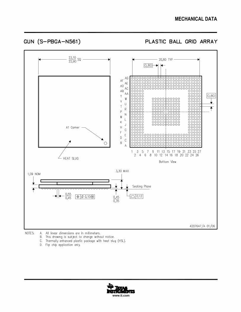

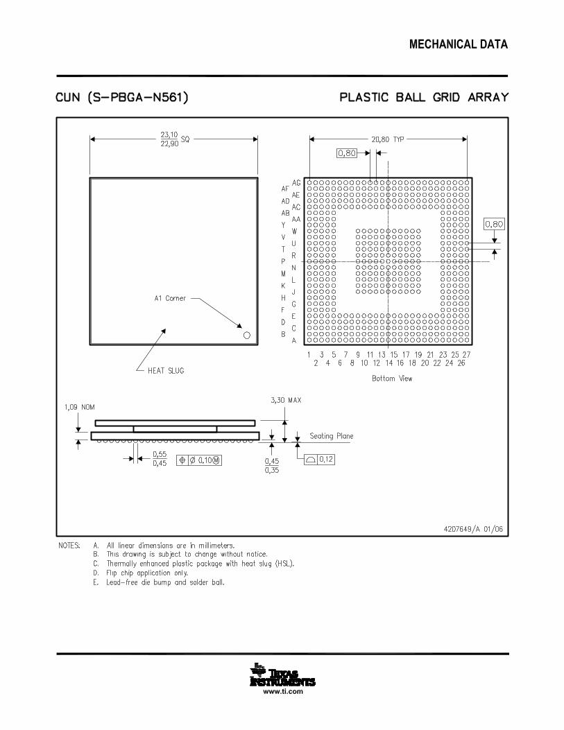
IMPORTANT NOTICE
Texas Instruments Incorporated and its subsidiaries (TI) reserve the right to make corrections, modifications, enhancements, improvements,and other changes to its products and services at any time and to discontinue any product or service without notice. Customers shouldobtain the latest relevant information before placing orders and should verify that such information is current and complete. All products aresold subject to TI’s terms and conditions of sale supplied at the time of order acknowledgment.
TI warrants performance of its hardware products to the specifications applicable at the time of sale in accordance with TI’s standardwarranty. Testing and other quality control techniques are used to the extent TI deems necessary to support this warranty. Except wheremandated by government requirements, testing of all parameters of each product is not necessarily performed.
TI assumes no liability for applications assistance or customer product design. Customers are responsible for their products andapplications using TI components. To minimize the risks associated with customer products and applications, customers should provideadequate design and operating safeguards.
TI does not warrant or represent that any license, either express or implied, is granted under any TI patent right, copyright, mask work right,or other TI intellectual property right relating to any combination, machine, or process in which TI products or services are used. Informationpublished by TI regarding third-party products or services does not constitute a license from TI to use such products or services or awarranty or endorsement thereof. Use of such information may require a license from a third party under the patents or other intellectualproperty of the third party, or a license from TI under the patents or other intellectual property of TI.
Reproduction of TI information in TI data books or data sheets is permissible only if reproduction is without alteration and is accompaniedby all associated warranties, conditions, limitations, and notices. Reproduction of this information with alteration is an unfair and deceptivebusiness practice. TI is not responsible or liable for such altered documentation. Information of third parties may be subject to additionalrestrictions.
Resale of TI products or services with statements different from or beyond the parameters stated by TI for that product or service voids allexpress and any implied warranties for the associated TI product or service and is an unfair and deceptive business practice. TI is notresponsible or liable for any such statements.
TI products are not authorized for use in safety-critical applications (such as life support) where a failure of the TI product would reasonablybe expected to cause severe personal injury or death, unless officers of the parties have executed an agreement specifically governingsuch use. Buyers represent that they have all necessary expertise in the safety and regulatory ramifications of their applications, andacknowledge and agree that they are solely responsible for all legal, regulatory and safety-related requirements concerning their productsand any use of TI products in such safety-critical applications, notwithstanding any applications-related information or support that may beprovided by TI. Further, Buyers must fully indemnify TI and its representatives against any damages arising out of the use of TI products insuch safety-critical applications.
TI products are neither designed nor intended for use in military/aerospace applications or environments unless the TI products arespecifically designated by TI as military-grade or "enhanced plastic." Only products designated by TI as military-grade meet militaryspecifications. Buyers acknowledge and agree that any such use of TI products which TI has not designated as military-grade is solely atthe Buyer's risk, and that they are solely responsible for compliance with all legal and regulatory requirements in connection with such use.
TI products are neither designed nor intended for use in automotive applications or environments unless the specific TI products aredesignated by TI as compliant with ISO/TS 16949 requirements. Buyers acknowledge and agree that, if they use any non-designatedproducts in automotive applications, TI will not be responsible for any failure to meet such requirements.
Following are URLs where you can obtain information on other Texas Instruments products and application solutions:
Products Applications
Audio www.ti.com/audio Communications and Telecom www.ti.com/communications
Amplifiers amplifier.ti.com Computers and Peripherals www.ti.com/computers
Data Converters dataconverter.ti.com Consumer Electronics www.ti.com/consumer-apps
DLP® Products www.dlp.com Energy and Lighting www.ti.com/energy
DSP dsp.ti.com Industrial www.ti.com/industrial
Clocks and Timers www.ti.com/clocks Medical www.ti.com/medical
Interface interface.ti.com Security www.ti.com/security
Logic logic.ti.com Space, Avionics and Defense www.ti.com/space-avionics-defense
Power Mgmt power.ti.com Transportation and www.ti.com/automotiveAutomotive
Microcontrollers microcontroller.ti.com Video and Imaging www.ti.com/video
RFID www.ti-rfid.com Wireless www.ti.com/wireless-apps
RF/IF and ZigBee® Solutions www.ti.com/lprf
TI E2E Community Home Page e2e.ti.com
Mailing Address: Texas Instruments, Post Office Box 655303, Dallas, Texas 75265Copyright © 2011, Texas Instruments Incorporated
Related Documents
![EC0804-PLL [Modo de compatibilidad]€¦ · (PLL) 1 Capítulo 4 Lazos enganchados en fase. PLL Aplicaciones de los PLL Síntesis de frecuencia Partiendo de un oscilador patrón (f0),](https://static.cupdf.com/doc/110x72/5e8e438d8741af3761030a0b/ec0804-pll-modo-de-compatibilidad-pll-1-captulo-4-lazos-enganchados-en-fase.jpg)